Embed Size (px)
Citation preview

TMS470R1x System ModuleReference Guide
Literature Number: SPNU189HNovember 2004

IMPORTANT NOTICE
Texas Instruments Incorporated and its subsidiaries (TI) reserve the right to make corrections,modifications, enhancements, improvements, and other changes to its products and services at any timeand to discontinue any product or service without notice. Customers should obtain the latest relevantinformation before placing orders and should verify that such information is current and complete. Allproducts are sold subject to TI's terms and conditions of sale supplied at the time of orderacknowledgment.
TI warrants performance of its hardware products to the specifications applicable at the time of sale inaccordance with TI's standard warranty. Testing and other quality control techniques are used to the extentTI deems necessary to support this warranty. Except where mandated by government requirements,testing of all parameters of each product is not necessarily performed.
TI assumes no liability for applications assistance or customer product design. Customers are responsiblefor their products and applications using TI components. To minimize the risks associated with customerproducts and applications, customers should provide adequate design and operating safeguards.
TI does not warrant or represent that any license, either express or implied, is granted under any TI patentright, copyright, mask work right, or other TI intellectual property right relating to any combination, machine,or process in which TI products or services are used. Information published by TI regarding third partyproducts or services does not constitute a license from TI to use such products or services or a warrantyor endorsement thereof. Use of such information may require a license from a third party under the patentsor other intellectual property of that third party, or a license from TI under the patents or other intellectualproperty of TI.
Reproduction of information in TI data books or data sheets is permissible only if reproduction is withoutalteration and is accompanied by all associated warranties, conditions, limitations, and notices.Reproduction of this information with alteration is an unfair and deceptive business practice. TI is notresponsible or liable for such altered documentation.
Resale of TI products or services with statements different from or beyond the parameters stated by TI forthat product or service voids all express and any implied warranties for the associated TI product or serviceand is an unfair and deceptive business practice. TI is not responsible or liable for any such statements.
Mailing Address: Texas InstrumentsPost Office Box 655303 Dallas, Texas 75265
Copyright © 2004, Texas Instruments Incorporated
Products Applications
Amplifiers amplifier.ti.com Audio www.ti.com/audioData Converters dataconverter.ti.com Automotive www.ti.com/automotiveDSP dsp.ti.com Broadband www.ti.com/broadbandInterface interface.ti.com Digital Control www.ti.com/digitalcontrolLogic logic.ti.com Military www.ti.com/militaryPower Mgmt power.ti.com Optical Networking www.ti.com/opticalnetworkMicrocontrollers microcontroller.ti.com Security www.ti.com/security
Telephony www.ti.com/telephony
Video & Imaging www.ti.com/video
Wireless www.ti.com/wireless

REVISION HISTORY
REVISION DATE NOTES
H 11/04 Release for mass market
G 4/04 Updates:“Analog RTI” , formerly section 5.4.4 , removed


Contents
1 System Module Overview . . . . . . . . . . . . . . . . . . . . . . . . . . . . . . . . . . . . . . . . . . . . . . . . . . . . . 22 Bus Structure . . . . . . . . . . . . . . . . . . . . . . . . . . . . . . . . . . . . . . . . . . . . . . . . . . . . . . . . . . . . . . . 7
2.1 CPU Bus. . . . . . . . . . . . . . . . . . . . . . . . . . . . . . . . . . . . . . . . . . . . . . . . . . . . . . . . . . . . . . 82.2 Expansion Bus . . . . . . . . . . . . . . . . . . . . . . . . . . . . . . . . . . . . . . . . . . . . . . . . . . . . . . . . . 8
2.2.1 Protocol for Memory Accesses on the Expansion Bus. . . . . . . . . . . . . . . . . . . . 82.2.2 Protocol for Peripheral Accesses on the Expansion Bus . . . . . . . . . . . . . . . . . 12
3 Memory . . . . . . . . . . . . . . . . . . . . . . . . . . . . . . . . . . . . . . . . . . . . . . . . . . . . . . . . . . . . . . . . . . . 143.1 Memory Map. . . . . . . . . . . . . . . . . . . . . . . . . . . . . . . . . . . . . . . . . . . . . . . . . . . . . . . . . . 143.2 Memory Selects . . . . . . . . . . . . . . . . . . . . . . . . . . . . . . . . . . . . . . . . . . . . . . . . . . . . . . . 15
3.2.1 Configuring Memory Selects . . . . . . . . . . . . . . . . . . . . . . . . . . . . . . . . . . . . . . 163.2.2 Enabling the Memory Map . . . . . . . . . . . . . . . . . . . . . . . . . . . . . . . . . . . . . . . . 173.2.3 Relocating Boot Memory . . . . . . . . . . . . . . . . . . . . . . . . . . . . . . . . . . . . . . . . . 18
3.3 Memory Protection . . . . . . . . . . . . . . . . . . . . . . . . . . . . . . . . . . . . . . . . . . . . . . . . . . . . . 193.3.1 Memory Block Protection . . . . . . . . . . . . . . . . . . . . . . . . . . . . . . . . . . . . . . . . . 193.3.2 Auxiliary Memory Protection—MPU for Internal RAM . . . . . . . . . . . . . . . . . . . 19
3.4 Memory Resets . . . . . . . . . . . . . . . . . . . . . . . . . . . . . . . . . . . . . . . . . . . . . . . . . . . . . . . 213.4.1 Illegal Address . . . . . . . . . . . . . . . . . . . . . . . . . . . . . . . . . . . . . . . . . . . . . . . . . 223.4.2 Illegal Access . . . . . . . . . . . . . . . . . . . . . . . . . . . . . . . . . . . . . . . . . . . . . . . . . . 223.4.3 Illegal Map . . . . . . . . . . . . . . . . . . . . . . . . . . . . . . . . . . . . . . . . . . . . . . . . . . . . 233.4.4 Peripheral Illegal Access . . . . . . . . . . . . . . . . . . . . . . . . . . . . . . . . . . . . . . . . . 23
4 Interrupts. . . . . . . . . . . . . . . . . . . . . . . . . . . . . . . . . . . . . . . . . . . . . . . . . . . . . . . . . . . . . . . . . . 254.1 Interrupt Handling at the CPU . . . . . . . . . . . . . . . . . . . . . . . . . . . . . . . . . . . . . . . . . . . . 254.2 Interrupt Generation at the Peripheral . . . . . . . . . . . . . . . . . . . . . . . . . . . . . . . . . . . . . . 254.3 CIM Interrupt Management. . . . . . . . . . . . . . . . . . . . . . . . . . . . . . . . . . . . . . . . . . . . . . . 26
4.3.1 CIM Input Channel Management . . . . . . . . . . . . . . . . . . . . . . . . . . . . . . . . . . . 274.3.2 CIM Prioritization . . . . . . . . . . . . . . . . . . . . . . . . . . . . . . . . . . . . . . . . . . . . . . . 274.3.3 CIM Operation . . . . . . . . . . . . . . . . . . . . . . . . . . . . . . . . . . . . . . . . . . . . . . . . . 27
4.4 System Software Interrupts (SSI) . . . . . . . . . . . . . . . . . . . . . . . . . . . . . . . . . . . . . . . . . . 295 Real-Time Interrupt (RTI) . . . . . . . . . . . . . . . . . . . . . . . . . . . . . . . . . . . . . . . . . . . . . . . . . . . . . 30
5.1 RTI Overview . . . . . . . . . . . . . . . . . . . . . . . . . . . . . . . . . . . . . . . . . . . . . . . . . . . . . . . . . 305.2 RTI Operating Modes and Conditions . . . . . . . . . . . . . . . . . . . . . . . . . . . . . . . . . . . . . . 30
5.2.1 RTI Module Clock Source. . . . . . . . . . . . . . . . . . . . . . . . . . . . . . . . . . . . . . . . . 315.3 RTI Operation . . . . . . . . . . . . . . . . . . . . . . . . . . . . . . . . . . . . . . . . . . . . . . . . . . . . . . . . . 31
5.3.1 Tap Interrupt . . . . . . . . . . . . . . . . . . . . . . . . . . . . . . . . . . . . . . . . . . . . . . . . . . . 335.3.2 Compare Interrupts. . . . . . . . . . . . . . . . . . . . . . . . . . . . . . . . . . . . . . . . . . . . . . 34
v

Contents
5.4 Analog Watchdog . . . . . . . . . . . . . . . . . . . . . . . . . . . . . . . . . . . . . . . . . . . . . . . . . . . . . . 355.4.1 AWD Threshold. . . . . . . . . . . . . . . . . . . . . . . . . . . . . . . . . . . . . . . . . . . . . . . . . 375.4.2 Effect of Pull-down . . . . . . . . . . . . . . . . . . . . . . . . . . . . . . . . . . . . . . . . . . . . . . 375.4.3 Effect of RDSON . . . . . . . . . . . . . . . . . . . . . . . . . . . . . . . . . . . . . . . . . . . . . . . . 39
6 Resets . . . . . . . . . . . . . . . . . . . . . . . . . . . . . . . . . . . . . . . . . . . . . . . . . . . . . . . . . . . . . . . . . . . . 417 Clocks . . . . . . . . . . . . . . . . . . . . . . . . . . . . . . . . . . . . . . . . . . . . . . . . . . . . . . . . . . . . . . . . . . . . 43
7.1 Low-Power Modes . . . . . . . . . . . . . . . . . . . . . . . . . . . . . . . . . . . . . . . . . . . . . . . . . . . . . 448 Parallel Signature Analyzer Overview. . . . . . . . . . . . . . . . . . . . . . . . . . . . . . . . . . . . . . . . . . . 46
8.1 PSA Updates. . . . . . . . . . . . . . . . . . . . . . . . . . . . . . . . . . . . . . . . . . . . . . . . . . . . . . . . . . 468.2 Read/Write Operation . . . . . . . . . . . . . . . . . . . . . . . . . . . . . . . . . . . . . . . . . . . . . . . . . . . 478.3 Emulation Support. . . . . . . . . . . . . . . . . . . . . . . . . . . . . . . . . . . . . . . . . . . . . . . . . . . . . . 478.4 Enable/Disable . . . . . . . . . . . . . . . . . . . . . . . . . . . . . . . . . . . . . . . . . . . . . . . . . . . . . . . . 478.5 PSA Pseudo Code . . . . . . . . . . . . . . . . . . . . . . . . . . . . . . . . . . . . . . . . . . . . . . . . . . . . . 47
9 Registers . . . . . . . . . . . . . . . . . . . . . . . . . . . . . . . . . . . . . . . . . . . . . . . . . . . . . . . . . . . . . . . . . . 499.1 MPU Address Registers . . . . . . . . . . . . . . . . . . . . . . . . . . . . . . . . . . . . . . . . . . . . . . . . . 65
9.1.1 MPU Address High Register (MPUAHRx) . . . . . . . . . . . . . . . . . . . . . . . . . . . . 669.1.2 MPU Address Low Register (MPUALRx) . . . . . . . . . . . . . . . . . . . . . . . . . . . . . 66
9.2 MPU Control Register . . . . . . . . . . . . . . . . . . . . . . . . . . . . . . . . . . . . . . . . . . . . . . . . . . . 679.2.1 MPU Control Register (MPUCTRL) . . . . . . . . . . . . . . . . . . . . . . . . . . . . . . . . . 67
9.3 Static Memory Control Registers . . . . . . . . . . . . . . . . . . . . . . . . . . . . . . . . . . . . . . . . . . 719.3.1 Static Memory Control Register 0 (SMCR0) . . . . . . . . . . . . . . . . . . . . . . . . . . . 729.3.2 Registers SMCR1-SMCR9 . . . . . . . . . . . . . . . . . . . . . . . . . . . . . . . . . . . . . . . . 749.3.3 Static Memory Control Registers (SMCRx). . . . . . . . . . . . . . . . . . . . . . . . . . . . 74
9.4 Write Control Register (WCR0) . . . . . . . . . . . . . . . . . . . . . . . . . . . . . . . . . . . . . . . . . . . 759.5 Peripheral Clock Register (PCR) . . . . . . . . . . . . . . . . . . . . . . . . . . . . . . . . . . . . . . . . . . 769.6 Peripheral Location Register (PLR) . . . . . . . . . . . . . . . . . . . . . . . . . . . . . . . . . . . . . . . . 789.7 Peripheral Protection Register (PPROT) . . . . . . . . . . . . . . . . . . . . . . . . . . . . . . . . . . . . 799.8 Memory Fine Base Address Registers . . . . . . . . . . . . . . . . . . . . . . . . . . . . . . . . . . . . . . 79
9.8.1 Memory Fine Base Address High Register 0 (MFBAHR0) . . . . . . . . . . . . . . . . 819.8.2 Memory Fine Base Address Low Register 0 (MFBALR0). . . . . . . . . . . . . . . . . 819.8.3 Memory Fine Base Address High Register (MFBAHRx). . . . . . . . . . . . . . . . . . 849.8.4 Memory Fine Base Address Low Register (MFBALRx) . . . . . . . . . . . . . . . . . . 84
9.9 Memory Coarse Select Control Registers. . . . . . . . . . . . . . . . . . . . . . . . . . . . . . . . . . . . 859.9.1 Memory Coarse Base Address High Register (MCBAHRx) . . . . . . . . . . . . . . . 869.9.2 Memory Coarse Base Address Low Register (MCBALRx) . . . . . . . . . . . . . . . . 86
9.10 RTI Counter (RTICNTR) . . . . . . . . . . . . . . . . . . . . . . . . . . . . . . . . . . . . . . . . . . . . . . . . . 899.11 RTI Preload Control Register (RTIPCTL) . . . . . . . . . . . . . . . . . . . . . . . . . . . . . . . . . . . . 909.12 RTI Control Register (RTICNTL). . . . . . . . . . . . . . . . . . . . . . . . . . . . . . . . . . . . . . . . . . . 929.13 Watchdog Key Register (WKEY) . . . . . . . . . . . . . . . . . . . . . . . . . . . . . . . . . . . . . . . . . . 939.14 RTI Compare Register 1(RTICMP1) . . . . . . . . . . . . . . . . . . . . . . . . . . . . . . . . . . . . . . . . 949.15 RTI Compare Register 2(RTICMP2) . . . . . . . . . . . . . . . . . . . . . . . . . . . . . . . . . . . . . . . . 949.16 Compare Interrupt Control Register (RTICINT) . . . . . . . . . . . . . . . . . . . . . . . . . . . . . . . 959.17 RTI Count Enable Register (RTICNTEN) . . . . . . . . . . . . . . . . . . . . . . . . . . . . . . . . . . . . 979.18 CIM Offset Vector Registers . . . . . . . . . . . . . . . . . . . . . . . . . . . . . . . . . . . . . . . . . . . . . . 97
9.18.1 IRQ Index Offset Vector Register (IRQIVEC) . . . . . . . . . . . . . . . . . . . . . . . . . . 989.18.2 FIQ Index Offset Vector Registers (FIQIVEC) . . . . . . . . . . . . . . . . . . . . . . . . . 99
vi

Contents
9.18.3 CIM Index Offset Vector Register (CIMIVEC) . . . . . . . . . . . . . . . . . . . . . . . . 1009.19 FIQ/IRQ Program Control Register (FIRQPR) . . . . . . . . . . . . . . . . . . . . . . . . . . . . . . . 1019.20 Pending Interrupt Read Location (INTREQ). . . . . . . . . . . . . . . . . . . . . . . . . . . . . . . . . 1019.21 Interrupt Mask Register (REQMASK). . . . . . . . . . . . . . . . . . . . . . . . . . . . . . . . . . . . . . 1029.22 CPU Data Bus Parallel Signature Analysis Register (CPUPSA) . . . . . . . . . . . . . . . . . 1039.23 PSA Enable (PSAENABLE) . . . . . . . . . . . . . . . . . . . . . . . . . . . . . . . . . . . . . . . . . . . . . 1039.24 New Global Control Register (GCR_N) . . . . . . . . . . . . . . . . . . . . . . . . . . . . . . . . . . . . 1049.25 Clock Control Register (CLKCNTL) . . . . . . . . . . . . . . . . . . . . . . . . . . . . . . . . . . . . . . . 1059.26 Global Control Register (GLBCTRL) . . . . . . . . . . . . . . . . . . . . . . . . . . . . . . . . . . . . . . 1089.27 System Exception Control Register (SYSECR) . . . . . . . . . . . . . . . . . . . . . . . . . . . . . . 1109.28 System Reset Exception Status Register (SYSESR). . . . . . . . . . . . . . . . . . . . . . . . . . 1129.29 Abort Exception Status Register (ABRTESR) . . . . . . . . . . . . . . . . . . . . . . . . . . . . . . . 1159.30 Global Status Register (GLBSTAT) . . . . . . . . . . . . . . . . . . . . . . . . . . . . . . . . . . . . . . . 1169.31 Device Identification Register (DEV) . . . . . . . . . . . . . . . . . . . . . . . . . . . . . . . . . . . . . . 1199.32 System Software Interrupt Flag Register (SSIF) . . . . . . . . . . . . . . . . . . . . . . . . . . . . . 1209.33 System Software Interrupt Request Register (SSIR) . . . . . . . . . . . . . . . . . . . . . . . . . . 121
Contents vii

viii
Figures
1 System Block Diagram . . . . . . . . . . . . . . . . . . . . . . . . . . . . . . . . . . . . . . . . . . . . . . . . . . . . . . . . 72 Zero Wait-State Memory Read Transaction . . . . . . . . . . . . . . . . . . . . . . . . . . . . . . . . . . . . . . . . 93 Zero Wait-State Memory Write Transaction . . . . . . . . . . . . . . . . . . . . . . . . . . . . . . . . . . . . . . . . 94 Leading Wait-State Memory Write Transaction. . . . . . . . . . . . . . . . . . . . . . . . . . . . . . . . . . . . . 105 Wait-State Memory Read Transaction . . . . . . . . . . . . . . . . . . . . . . . . . . . . . . . . . . . . . . . . . . . 106 Wait-State Memory Write Transaction . . . . . . . . . . . . . . . . . . . . . . . . . . . . . . . . . . . . . . . . . . . 117 Trailing Wait-State Memory Read Transaction . . . . . . . . . . . . . . . . . . . . . . . . . . . . . . . . . . . . . 118 Trailing Wait-State Memory Write Transaction . . . . . . . . . . . . . . . . . . . . . . . . . . . . . . . . . . . . . 129 Generic Device Memory Map . . . . . . . . . . . . . . . . . . . . . . . . . . . . . . . . . . . . . . . . . . . . . . . . . . 1510 Memory Map After Reset . . . . . . . . . . . . . . . . . . . . . . . . . . . . . . . . . . . . . . . . . . . . . . . . . . . . . 1611 Sample Memory Map After Memory Map is Configured and Enabled . . . . . . . . . . . . . . . . . . . 1712 Memory Mapping Scheme for Relocating Boot Memory . . . . . . . . . . . . . . . . . . . . . . . . . . . . . 1813 MPU Address Decode . . . . . . . . . . . . . . . . . . . . . . . . . . . . . . . . . . . . . . . . . . . . . . . . . . . . . . . 2014 Typical Operating System Use of the MPU. . . . . . . . . . . . . . . . . . . . . . . . . . . . . . . . . . . . . . . . 2115 Central Interrupt Manager (CIM) Block Diagram. . . . . . . . . . . . . . . . . . . . . . . . . . . . . . . . . . . . 2616 RTI Block Diagram . . . . . . . . . . . . . . . . . . . . . . . . . . . . . . . . . . . . . . . . . . . . . . . . . . . . . . . . . . 3217 External Required Circuit for Watchdog . . . . . . . . . . . . . . . . . . . . . . . . . . . . . . . . . . . . . . . . . . 3518 AWD Threshold. . . . . . . . . . . . . . . . . . . . . . . . . . . . . . . . . . . . . . . . . . . . . . . . . . . . . . . . . . . . . 3719 Effect of Pull-down . . . . . . . . . . . . . . . . . . . . . . . . . . . . . . . . . . . . . . . . . . . . . . . . . . . . . . . . . . 3820 Sequential AWD Charge/Discharge Cycles Reach Charge Asymptote . . . . . . . . . . . . . . . . . . 3921 PSA Operation . . . . . . . . . . . . . . . . . . . . . . . . . . . . . . . . . . . . . . . . . . . . . . . . . . . . . . . . . . . . . 4622 MPU Register Alignment with Address Bus . . . . . . . . . . . . . . . . . . . . . . . . . . . . . . . . . . . . . . . 65

Tables
1 System Module Overview. . . . . . . . . . . . . . . . . . . . . . . . . . . . . . . . . . . . . . . . . . . . . . . . . . . . . . 22 System Module Internal Registers . . . . . . . . . . . . . . . . . . . . . . . . . . . . . . . . . . . . . . . . . . . . . . . 23 Aligned Address Boundary by Access Type. . . . . . . . . . . . . . . . . . . . . . . . . . . . . . . . . . . . . . . . 94 Priority of Control Register Bits for Overlapping Channels . . . . . . . . . . . . . . . . . . . . . . . . . . . 215 Memory Reset/Abort Causes and Their Associated Exception Flag . . . . . . . . . . . . . . . . . . . . 246 RTI Operating Modes . . . . . . . . . . . . . . . . . . . . . . . . . . . . . . . . . . . . . . . . . . . . . . . . . . . . . . . . 307 PLL State During Standby Mode . . . . . . . . . . . . . . . . . . . . . . . . . . . . . . . . . . . . . . . . . . . . . . . 318 Tap Interrupts . . . . . . . . . . . . . . . . . . . . . . . . . . . . . . . . . . . . . . . . . . . . . . . . . . . . . . . . . . . . . . 349 Example WKEY Register Sequence . . . . . . . . . . . . . . . . . . . . . . . . . . . . . . . . . . . . . . . . . . . . 3610 Maximum Resistance by Buffer Strength . . . . . . . . . . . . . . . . . . . . . . . . . . . . . . . . . . . . . . . . . 3911 RC Discharge Curve . . . . . . . . . . . . . . . . . . . . . . . . . . . . . . . . . . . . . . . . . . . . . . . . . . . . . . . . 4012 Causes of TMS470R1x Reset/Abort . . . . . . . . . . . . . . . . . . . . . . . . . . . . . . . . . . . . . . . . . . . . 4113 Clock Domains . . . . . . . . . . . . . . . . . . . . . . . . . . . . . . . . . . . . . . . . . . . . . . . . . . . . . . . . . . . . . 4314 Active Clock Domains and Device Condition . . . . . . . . . . . . . . . . . . . . . . . . . . . . . . . . . . . . . . 4415 System Register Accessibility . . . . . . . . . . . . . . . . . . . . . . . . . . . . . . . . . . . . . . . . . . . . . . . . . 4916 Control Register Map . . . . . . . . . . . . . . . . . . . . . . . . . . . . . . . . . . . . . . . . . . . . . . . . . . . . . . . . 5017 MPU Registers . . . . . . . . . . . . . . . . . . . . . . . . . . . . . . . . . . . . . . . . . . . . . . . . . . . . . . . . . . . . . 6518 Static Memory Control Register Starting Addresses . . . . . . . . . . . . . . . . . . . . . . . . . . . . . . . . 7119 Wait State Definition for Memory Bank0 . . . . . . . . . . . . . . . . . . . . . . . . . . . . . . . . . . . . . . . . . 7320 Data Widths for Data Memory Bank0. . . . . . . . . . . . . . . . . . . . . . . . . . . . . . . . . . . . . . . . . . . . 7421 Peripheral Clock Division Ratios . . . . . . . . . . . . . . . . . . . . . . . . . . . . . . . . . . . . . . . . . . . . . . . 7722 Fine Base Control Register Addresses . . . . . . . . . . . . . . . . . . . . . . . . . . . . . . . . . . . . . . . . . . 8023 Block Size Bit Encoding (Fine Memory Selects) . . . . . . . . . . . . . . . . . . . . . . . . . . . . . . . . . . . 8224 Coarse Base Control Register Addresses . . . . . . . . . . . . . . . . . . . . . . . . . . . . . . . . . . . . . . . . 8525 Block Size Bit Encoding (for Coarse Selects). . . . . . . . . . . . . . . . . . . . . . . . . . . . . . . . . . . . . . 8826 Tap Interrupts . . . . . . . . . . . . . . . . . . . . . . . . . . . . . . . . . . . . . . . . . . . . . . . . . . . . . . . . . . . . . . 9127 Example of a WKEY Sequence . . . . . . . . . . . . . . . . . . . . . . . . . . . . . . . . . . . . . . . . . . . . . . . . 9328 Real-Time Interrupt Counter Enable Modes. . . . . . . . . . . . . . . . . . . . . . . . . . . . . . . . . . . . . . . 9729 Interrupt Dispatch Table . . . . . . . . . . . . . . . . . . . . . . . . . . . . . . . . . . . . . . . . . . . . . . . . . . . . . . 9830 CLKOUT Values . . . . . . . . . . . . . . . . . . . . . . . . . . . . . . . . . . . . . . . . . . . . . . . . . . . . . . . . . . . 107
ix

31 Wake-up Interrupt Reset Modes . . . . . . . . . . . . . . . . . . . . . . . . . . . . . . . . . . . . . . . . . . . . . . . 107
x
System Module
The system module provides an interface from the ARM CPU to the TexasInstruments (TI) TMS470R1x family of devices. The module defines the CPUbus and the expansion bus. The system module is responsible for memoryinterface and protection, interrupt prioritization, reset generation, and clocksynthesis.
1 System Module Overview . . . . . . . . . . . . . . . . . . . . . . . . . . . . . . . . . . . . 2
2 Bus Structure . . . . . . . . . . . . . . . . . . . . . . . . . . . . . . . . . . . . . . . . . . . . . . 7
3 Memory . . . . . . . . . . . . . . . . . . . . . . . . . . . . . . . . . . . . . . . . . . . . . . . . . . 14
4 Interrupts . . . . . . . . . . . . . . . . . . . . . . . . . . . . . . . . . . . . . . . . . . . . . . . . 25
5 Real-Time Interrupt (RTI) . . . . . . . . . . . . . . . . . . . . . . . . . . . . . . . . . . . . 30
6 Resets . . . . . . . . . . . . . . . . . . . . . . . . . . . . . . . . . . . . . . . . . . . . . . . . . . . 41
7 Clocks . . . . . . . . . . . . . . . . . . . . . . . . . . . . . . . . . . . . . . . . . . . . . . . . . . . 43
8 Parallel Signature Analyzer Overview . . . . . . . . . . . . . . . . . . . . . . . . . 46
9 Registers. . . . . . . . . . . . . . . . . . . . . . . . . . . . . . . . . . . . . . . . . . . . . . . . . 49
Topic Page
1
System Module Overview
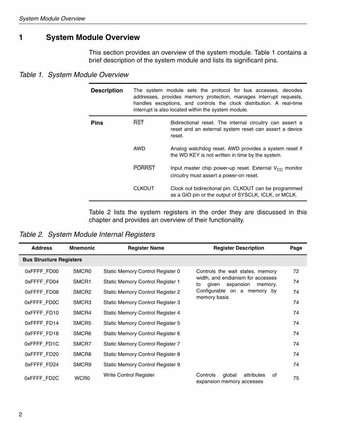
1 System Module Overview
This section provides an overview of the system module. Table 1 contains abrief description of the system module and lists its significant pins.
Table 2 lists the system registers in the order they are discussed in thischapter and provides an overview of their functionality.
Table 1. System Module Overview
Description The system module sets the protocol for bus accesses, decodesaddresses, provides memory protection, manages interrupt requests,handles exceptions, and controls the clock distribution. A real-timeinterrupt is also located within the system module.
Pins RST Bidirectional reset. The internal circuitry can assert areset and an external system reset can assert a devicereset.
AWD Analog watchdog reset. AWD provides a system reset ifthe WD KEY is not written in time by the system.
PORRST Input master chip power-up reset. External VCC monitorcircuitry must assert a power-on reset.
CLKOUT Clock out bidirectional pin. CLKOUT can be programmedas a GIO pin or the output of SYSCLK, ICLK, or MCLK.
Table 2. System Module Internal Registers
Address Mnemonic Register Name Register Description Page
Bus Structure Registers
0xFFFF_FD00 SMCR0 Static Memory Control Register 0 Controls the wait states, memorywidth, and endianism for accessesto given expansion memory.Configurable on a memory bymemory basis
72
0xFFFF_FD04 SMCR1 Static Memory Control Register 1 74
0xFFFF_FD08 SMCR2 Static Memory Control Register 2 74
0xFFFF_FD0C SMCR3 Static Memory Control Register 3 74
0xFFFF_FD10 SMCR4 Static Memory Control Register 4 74
0xFFFF_FD14 SMCR5 Static Memory Control Register 5 74
0xFFFF_FD18 SMCR6 Static Memory Control Register 6 74
0xFFFF_FD1C SMCR7 Static Memory Control Register 7 74
0xFFFF_FD20 SMCR8 Static Memory Control Register 8 74
0xFFFF_FD24 SMCR9 Static Memory Control Register 9 74
0xFFFF_FD2C WCR0Write Control Register Controls global attributes of
expansion memory accesses75
2

System Module Overview
Bus Structure Registers (Continued)
0xFFFF_FD34 PLRPeripheral Location Register Configures the peripheral as
internal/external78
0xFFFF_FD38 PPROTPeripheral Protection Register Controls whether peripherals may
be addressed in privilege modeonly or in user and privilege mode
79
Memory Registers
0xFFFF_FE00 MFBAHR0Memory Fine Base Address HighRegister 0
Memory Fine Base Address Highand Memory Fine Base AddressLow registers configure thememory-select signals. The baseaddress, block size, and protectionfor the associated memory are setin these registers.
Memory Fine Base Address LowRegister 0 contains the memory-select bit that enables the memorymaps as configured through thememory fine base address andmemory coarse base addressregisters.
81
0xFFFF_FE04 MFBALR0Memory Fine Base Address LowRegister 0
81
0xFFFF_FE08 MFBAHR1Memory Fine Base Address HighRegister 1
84
0xFFFF_FE0C MFBALR1Memory Fine Base Address LowRegister 1
84
0xFFFF_FE10 MFBAHR2Memory Fine Base Address HighRegister 2
84
0xFFFF_FE14 MFBALR2Memory Fine Base Address LowRegister 2
84
0xFFFF_FE18 MFBAHR3Memory Fine Base Address HighRegister 3
84
0xFFFF_FE1C MFBALR3Memory Fine Base Address LowRegister 3
84
0xFFFF_FE20 MFBAHR4Memory Fine Base Address HighRegister 4
84
0xFFFF_FE24 MFBALR4Memory Fine Base Address LowRegister 4
84
0xFFFF_FE28 MFBAHR5Memory Fine Base Address HighRegister 5
84
0xFFFF_FE2C MFBALR5Memory Fine Base Address LowRegister 5
84
0xFFFF_FE30 MCBAHR0Memory Coarse Base AddressHigh Register 0
86
0xFFFF_FE34 MCBALR0Memory Coarse Base AddressLow Register 0
86
Table 2. System Module Internal Registers (Continued)
Address Mnemonic Register Name Register Description Page
System Module (SPNU189H) 3

System Module Overview
Memory Registers (Continued)
0xFFFF_F38 MCBAHR1Memory Coarse Base AddressHigh Register 1
Memory Fine Base Address Highand Memory Fine Base AddressLow registers configure thememory-select signals. The baseaddress, block size, and protectionfor the associated memory are setin these registers.
Memory Fine Base Address LowRegister 0 contains the memory-select bit that enables the memorymaps as configured through thememory fine base address andmemory coarse base addressregisters.
86
0xFFFF_FE3C MCBALR1Memory Coarse Base AddressLow Register 1
86
0xFFFF_FE40 MCBAHR2Memory Coarse Base AddressHigh Register 2
86
0xFFFF_FE44 MCBALR2Memory Coarse Base AddressLow Register 2
86
0xFFFF_FE48 MCBAHR3Memory Coarse Base AddressHigh Register 3
86
0xFFFF_FE4C MCBALR3Memory Coarse Base AddressLow Register 3
86
0xFFFF_FE50 MCBAHR4Memory Coarse Base AddressHigh Register 4
86
0xFFFF_FE54 MCBALR4Memory Coarse Base AddressLow Register 4
86
0xFFFF_FE58 MCBAHR5Memory Coarse Base AddressHigh Register 5
86
0xFFFF_FE5C MCBALR5Memory Coarse Base AddressLow Register 5
86
Memory Protection Unit (MPU) Address Registers (Offset Address)
0x00 MPUAHR0 MPU Address High Register 0 66
0x04 MPUALR0 MPU Address Low Register 0 66
0x08 MPUAHR1 MPU Address High Register 1 MPU Address High and MPUAddress Low Registers configurethe address range to be protectedby the MPU. The MPU channel isenabled (and the channel’sprotection set) within the MPUcontrol register
66
0x0C MPUALR1 MPU Address Low Register 1 66
0x10 MPUAHR2 MPU Address High Register 2 66
0x14 MPUALR2 MPU Address Low Register 2 66
0x18 MPUAHR3 MPU Address High Register 3 66
0x1C MPUALR3 MPU Address Low Register 3 66
0x20 MPUCTRLMPU Control Register Controls the channel’s protection
and enable67
Table 2. System Module Internal Registers (Continued)
Address Mnemonic Register Name Register Description Page
4

System Module Overview
Interrupts
0xFFFF_FF20 IRQIVECIRQ Index Offset Vector Register Provides a numerical offset to the
highest priority pending interruptrequest (IRQ) interrupt
98
0xFFFF_FF24 FIQIVECFIQ Index Offset Vector Register Provides a numerical offset to the
highest priority pending fastinterrupt request (FIQ) interrupt
99
0xFFFF_FF28 CIMIVECCIM Index Offset Vector Register Provides a numerical offset to the
highest priority pending interrupt100
0xFFFF_FF2C FIRQPRFIQ/IRQ Program Control Register Controls whether the request
channel generates an IRQ or anFIQ request to the CPU
101
0xFFFF_FF30 INTREQPending Interrupt Read LocationRegister
Shows the pending interrupts101
0xFFFF_FF34 REQMASK Interrupt Mask Register Enables interrupt request channels 102
0xFFFF_FFF8 SSIFSystem Software Interrupt FlagRegister
Flag for software interrupt120
0xFFFF_FFFC SSIRSystem Software Interrupt RequestRegister
Generates software interrupt121
Real-Time Interrupt (RTI) Registers
0xFFFF_FF00 RTICNTRRTI Counter Contains MOD and CNTR
counters for the RTI89
0xFFFF_FF4RTI
PCTLRTI Preload Control Register Controls the MOD preload value
and tap interrupt selection90
0xFFFF_FF08RTI
CNTLRTI Control Register Contains tap interrupt flag and
enable92
0xFFFF_FF0C WKEYWatchdog Key Register Correct sequence written to this
register discharges the watchdogcapacitor.
93
0xFFFF_FF10RTI
CMP1RTI Compare Register 1 Contains value to compare to
CNTR.94
0xFFFF_FF14RTI
CMP2RTI Compare Register 2 Contains value to compare to
CNTR.94
0xFFFF_FF18RTI
CINT
RTI Compare Interrupt ControlRegister
Contains enables and flags forcompare 1 and compare 2interrupts
95
0xFFFF_FF1CRTI
CNTENRTI Counter Enable Register Enables the RTI counter based
upon the CPU operating mode97
Table 2. System Module Internal Registers (Continued)
Address Mnemonic Register Name Register Description Page
System Module (SPNU189H) 5

System Module Overview
Clock Registers
0xFFFF_FD30 PCRPeripheral Clock Register Contains the ICLK divider and
peripheral enable76
0xFFFF_FFD0 CLKCNTLClock Control Register Controls CLKOUT pin, peripheral
power down, and device low powermodes
105
0xFFFF_FFDC GLBCTRLGlobal Control Register Contains PLL-specific bits as well
as the flash memory configurationbit
108
Reset Registers
0xFFFF_FFE0 SYSECR System Exception Control Register Contains software reset 110
0xFFFF_FFE4 SYSESRSystem Reset Exception StatusRegister
Contains reset flags112
0xFFFF_FFE8 ABRTESR Abort Exception Status Register Contains abort flags 115
0xFFFF_FFEC GLBSTATGlobal Status Register Contains bits that determine the
source of illegal address, illegalaccess and clock reset exceptions
116
Parallel Signature Analysis (PSA) Registers
0xFFFF_FF40CPUPSA
CPU Data Bus PSA Registers Contains the signature value forthe PSA
103
0xFFFF_FF50PSA
DISABLEPSA Enable Contains PSA enable bit
103
Miscellaneous Registers
0xFFFF_FFF0 DEVDevice Identification Register Contains device-specific
information hard-coded duringdevice manufacture
119
Table 2. System Module Internal Registers (Continued)
Address Mnemonic Register Name Register Description Page
6

Bus Structure
2 Bus Structure
The system module defines two independent buses: a CPU bus and anexpansion bus. The memory arrays (flash, ROM and RAM), CPU, DMA, andsystem module connect to the CPU bus. The system module, DMA,expansion peripherals, and expansion memories (for example, HET RAM)connect to the expansion bus. These buses are illustrated in Figure 1. Thissection (bus structure) discusses the protocol on the separate buses.
CPU bus protocol Expansion bus protocol
Protocol for memory accesses on expansion bus Protocol for peripheral accesses on expansion bus
Figure 1. System Block Diagram
RAM(4K)
CPU Bus
TMS470R1x SYSTEM MODULE
ExternalPins
FLASH/ROM
4 Sectors
ExternalPins
TMS470R1x CPU
PERIPHERAL 1
PERIPHERAL 2
PERIPHERAL 3
PERIPHERAL 4
MEMORY
Exp
ansi
on
Bu
s
System Module (SPNU189H) 7

Bus Structure
2.1 CPU Bus
The CPU bus connects the central processor to its tightly coupled memories(that is, ROM, RAM, flash). In general, the CPU bus is a high-speed, internalbus. The system module acts as a bridge between the CPU and theexpansion buses.
2.2 Expansion Bus
While the CPU bus protocol is fixed, the expansion bus protocol isconfigurable. The expansion bus supports protocol for interfacing to:
Memory Peripherals
2.2.1 Protocol for Memory Accesses on the Expansion Bus
Memory accesses on the expansion bus are carried out at the SYSCLKfrequency. The WCR0 register contains bits that control the global propertiesof the expansion bus protocol for memory; you can enable a write buffer thatallows the CPU to write to the expansion bus and the CPU can perform otheractions (not on the expansion bus) while the wait state is ongoing. You mustconfigure the WCR0 register so that the expansion bus protocol isappropriate for the accessed memory.
Additionally, each memory select may be configured uniquely for the memoryaccessed through the expansion bus. Each SMCRx register configures theexpansion bus separately for specific data widths and wait states. Themapping of SMCRx registers to different memory selects is device specific.(See the device-specific data sheet for additional details.)
Data Width
The expansion bus supports 8-bit, 16-bit, and 32-bit read/write operations toall memory modules. You configure the data width of the memory region withthe DW bit field (SMCRx.1:0) as shown in Table 3. (The system moduleautomatically configures the DW bit field for SMCR0 during reset.) Nounaligned memory accesses are permitted.
Memory Select:Memory selects allow the user to place physical memory within the address space at user-defined addresses. The memory selects are configured by the MFBAHRx, MFBALRx, MCBAHRx, and MCBALRx registers (see section 9.8).
8

Bus Structure
Memory Wait States
The expansion bus can support zero wait states, but it also supports waitstates on the address setup, during the memory access, and on the trailingedge in order to meet the memory requirements of the expansion busmemory. These wait states are summed together. The memory access timingcan be customized on a memory select by programming the ASC, WS, andTWS bits of the appropriate SMCRx register. Figure 2 and Figure 3 illustratethe timing of the zero wait state memory read and write transaction,respectively.
Note: The timings in Figure 2 through Figure 8 are presented for reference.The signal behavior should be verified in the device data sheet.
Figure 2. Zero Wait-State Memory Read Transaction
Figure 3. Zero Wait-State Memory Write Transaction
Table 3. Aligned Address Boundary by Access Type
Read/Write Access Aligned Address Boundary
8-bit Any boundary (0x00, 0x01, 0x02, 0x03,...)
16-bit Any even boundary (0x00, 0x02, 0x04, 0x06,...)
32-bit Any multiple of 4 (0x00, 0x04, 0x08, 0x0C)
SYSCLK
CS
ADDR
OE
DATA
SYSCLK
CS
ADDR
WR
DATA
System Module (SPNU189H) 9

Bus Structure
Address setup wait states are programmed into the ASC bit field(SMCRx.13:12).
Read:
The ASC wait states do not affect read accesses.
Figure 4 illustrates the leading wait-state memory write transaction.
Figure 4. Leading Wait-State Memory Write Transaction
The memory select (CS) is active and the data is valid ASC SYSCLKcycles before the write strobe (WR) is asserted.
The address setup wait states support flexible WR setup timerequirements for write operations.
Wait states during the memory access are programmed into the WS.3:0 bitfield (SMCRx.7:4). For devices with 470+ architecture, there is a minimumof one wait state.
Figure 5 illustrates the wait-state memory read transaction.
Figure 5. Wait-State Memory Read Transaction
The memory select (CS), output enable (OE), and data are valid atthe same time. These signals are stretched for WS SYSCLK cycles.
SYSCLK
CS
ADDR
WR
DATA
Two leading wait states
SYSCLK
CS
ADDR
OE
DATA
Two wait states
10

Bus Structure
The wait states support slow read/write accesses.
Figure 6 illustrates the wait-state memory write transaction.
Figure 6. Wait-State Memory Write Transaction
The memory select (CS), write strobe (WR), and data are valid at thesame time. These signals are stretched for WS SYSCLK cycles.
The wait states support slow read/write accesses.
Trailing edge wait states are programmed into the TWS bit field(SMCRx.11:9). Write accesses on the expansion bus have at least onetrailing wait state unless TWS is cleared to 0x00 and the WTWSOVR bitfield (WCR0.1) is set to 1.
Figure 7 illustrates the trailing wait-state memory read transaction.
Figure 7. Trailing Wait-State Memory Read Transaction
The memory select (CS), output enable (OE), and data are valid atthe same time. The expansion bus is held for TWS SYSCLK cycles,but there are no wait states at the CPU unless another expansion busaccess is required prior to the completion of the trailing wait states.
SYSCLK
CS
ADDR
WR
DATA
Two wait states
SYSCLK
CS
ADDR
OE
DATA
Two trailing wait states
System Module (SPNU189H) 11

Bus Structure
The trailing wait states prevent bus drive conflicts from memories withslow output disables. A slow output disable is not a concern for bytereads to the same memory. Byte reads do not have trailing wait statesbetween the byte reads because the same memory does not requirethe output disable.
Figure 8 illustrates the trailing wait-state memory write transaction.
Figure 8. Trailing Wait-State Memory Write Transaction
The memory select (CS), write strobe (WR), and data are valid at thesame time. The memory select and data are stretched by TWSSYSCLK cycles. The write strobe goes inactive TWS SYSCLK cyclesbefore the memory select and the data.
The trailing wait state supports flexible hold times for writeoperations.
The expansion bus can be used for off-chip memory accesses (if the busis brought external). The location of the memory (on chip or external) isconfigured in the MLOC bit field (SMCRx.2 [in this case x cannot be 0].)
The system allows for interfacing to different endian memories. Theendianism of the expansion memory is programmed into the END bit field(SMCRx.3 [in this case x cannot be 0].)
Expansion bus frequency is SYSCLK frequency for memory accesses.
2.2.2 Protocol for Peripheral Accesses on the Expansion Bus
Peripheral accesses on the expansion bus are carried out at the ICLKfrequency (see Section 7, Clocks, on page 43). The expansion bus protocolfor peripheral access is handled by the system module.
The expansion bus supports 8-bit, 16-bit, and 32-bit read/write operationsto all peripheral modules. (However, the peripheral itself may not support8-bit, 16-bit, and 32-bit read/write operations.)
Two trailing wait states
SYSCLK
CS
ADDR
WR
DATA
12

Bus Structure
The expansion bus can be used for off-chip peripheral accesses (if the busis brought external). The location of the peripheral (on chip or external) isconfigured in the PLR register.
The peripheral control registers may be protected on a peripheral-by-peripheral basis through the peripheral protection register, PPROT. Theperipheral protection register allows the user to restrict access to theperipherals based upon whether the ARM CPU is in user mode.
The peripheral modules (including HET) are held in reset until thePENABLE bit (PCR.0) is set.
ICLK is generated from SYSCLK. The ICLK frequency is determined by theCLKDIV bit field (PCR.4:1); the system divides the SYSCLK frequency togenerate ICLK for reduced power.
ICLK is not guaranteed to be a 50% duty cycle.
Peripheral accesses are measured in terms of ICLK.
Peripheral reads take a minimum of 2 ICLK cycles.
Peripheral writes take a minimum of 2 ICLK + 1 SYSCLK cycles.
If ICLK is divided down from SYSCLK (that is, CLKDIV ≠ 0x00), thesystem asserts wait states at the beginning of the peripheral access, ifrequired, so that the access begins on an ICLK boundary.
System Module (SPNU189H) 13

Memory
3 Memory
The memory arrays have a user-defined address. The memory sectiondiscusses:
How the memory arrays are addressed within the overall memory map ofthe device
Protection for these memory arrays
3.1 Memory Map
A generic device memory map is shown in Figure 9. The physical memory ofthe device (control registers, flash memory, ROM, and RAM) must beaddressed within this memory map. The control registers are located at fixedaddresses that are device specific. (See the device-specific data sheet for themapping of peripherals to the peripheral selects.) 1K-byte sections of thememory map are reserved for each peripheral’s control registers, and these1-Kbyte sections of memory are accessed through a peripheral select.
The system control registers and flash control registers are located in theupper 2M bytes of the memory map. System control registers (except for theMPU) are located from 0xFFFF_FFFF to 0xFFFF_FD00. In addition to thecontrol registers, the exception vectors have a fixed map from 0x1F to 0x00.These vectors are shown in Figure 9. These control registers and vectoraddresses are always valid. To access the peripheral control registers, theperipheral must be released from reset by setting PENABLE to 1 (PCR.0 = 1).
There are exceptions that consist of reset, undefined instruction, softwareinterrupt, prefetch, abort, data abort, IRQ, and FIQ. Each of these exceptionshas its own vector.
Address Space:The address space is the set of all possible unique addresses. For the 470R1x family of devices, the memory map is 4G bytes because of the 32-bit architecture.
Memory Map:The memory map shows where the memory is located within the address space.
Peripheral Select:The system module decodes the top 22 bits of the address bus. If the address lies between addresses 0xFFF7_FFFF and 0xFFF7_C000, then the system sends a peripheral-select signal plus the bottom 10 bits of the address bus to the selected peripheral.
14

Memory
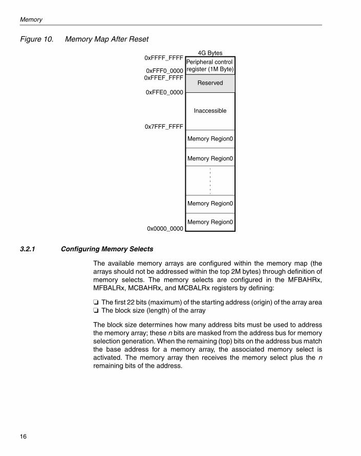
Figure 9. Generic Device Memory Map
3.2 Memory Selects
After reset, the memory map control registers for flash, system, andperipherals are all valid. Valid too are the exception vectors located from 0x1Fto 0x00. Additionally, the entire flash or ROM is available. This flash or ROMis mirrored throughout the bottom 2G bytes of the memory map. (See Figure10.)
0xFFFF_FFFF System Module Control Registers
(512K Bytes)
Exception, Interrupt, andReset Vectors
Memory (4G Bytes)
Programand
Data Area
Peripheral Control Reg-isters
(512K Bytes)
Reserved
MPU Control Registers
Reserved
0xFFF8_0000 0xFFF7_FFFF
0xFFF0_0000
0xFFE0_0000
0x0000_00200x0000_001F
0x0000_0000
FIQIRQ
ReservedData Abort
Prefetch AbortSoftware Interrupt
Undefined InstructionReset
0x0000_001C
0x0000_0018
0x0000_0014
0x0000_0010
0x0000_000C
0x0000_00080x0000_0004
0x0000_0000
0xFFFF_FFFF
0xFFF8_0000
PERIPHERAL SELECT 0 0xFFF7_FFFF0xFFF7_FC00
0xFFF7_F800
0xFFF7_F400
0xFFF7_F000
0xFFF7_EC00
0xFFF7_E800
0xFFF7_E400
RAM†
FLASH†or
Flash Control Registers
Reserved0xFFEF_FFFF
Reserved
0xFFDF_FFF
0xFFF7_E000
0xFFF7_DC00
0xFFF7_D800
0xFFF7_D400
0xFFF7_D000
0xFFF7_CC00
0xFFF7_C800
0xFFF7_C400
0xFFF7_C000
0xFFF7_0000
SYSTEM
PERIPHERAL SELECT 1
PERIPHERAL SELECT 2
PERIPHERAL SELECT 3
PERIPHERAL SELECT 4PERIPHERAL SELECT 5
PERIPHERAL SELECT 6
PERIPHERAL SELECT 7PERIPHERAL SELECT 8
PERIPHERAL SELECT 9
PERIPHERAL SELECT 10
PERIPHERAL SELECT 11
PERIPHERAL SELECT 12
PERIPHERAL SELECT 13
PERIPHERAL SELECT 14
PERIPHERAL SELECT 150xFFF7_B7FF
† The base address for the flash and RAM is programmable.
Reserved
ROM
System Module (SPNU189H) 15
Memory
Figure 10. Memory Map After Reset
3.2.1 Configuring Memory Selects
The available memory arrays are configured within the memory map (thearrays should not be addressed within the top 2M bytes) through definition ofmemory selects. The memory selects are configured in the MFBAHRx,MFBALRx, MCBAHRx, and MCBALRx registers by defining:
The first 22 bits (maximum) of the starting address (origin) of the array area The block size (length) of the array
The block size determines how many address bits must be used to addressthe memory array; these n bits are masked from the address bus for memoryselection generation. When the remaining (top) bits on the address bus matchthe base address for a memory array, the associated memory select isactivated. The memory array then receives the memory select plus the nremaining bits of the address.
4G Bytes0xFFFF_FFFF
0xFFEF_FFFF0xFFF0_0000
0xFFE0_0000
0x7FFF_FFFF
0x0000_0000
Peripheral control
Inaccessible
Memory Region0
Memory Region0
Memory Region0
Memory Region0
Reserved
register (1M Byte)
16

Memory
Note: Base Address Must be a Multiple of the Block Size
The details concerning how the system generates memory selects can besummarized with the rule that the base address must be a multiple of theblock size.
3.2.2 Enabling the Memory Map
All memory selects except memory select 0 (attached to boot) are disabledat reset. The boot program should set up the memory base address controlregisters (configure all memory selects) and then set the memory map selectbit in the memory base address register 0 (MFBALR0.8). Once the memorymap select bit is set, the memory selects are generated based on the contentof the memory base address registers.
The memory map is activated when the memory map select bit (MFBALR0.8)is set. Figure 11 shows an example of an enabled memory map.
Figure 11. Sample Memory Map After Memory Map is Configured and Enabled
4G Bytes0xFFFF_FFFF
0xFFEF_FFFF0xFFF0_0000
0xFFE0_0000
0x0000_0000
Peripheral control register (1M Byte)
Memory Region4
Memory Region3
Memory Region2
Memory Region1
Reserved
Memory Region0
System Module (SPNU189H) 17

Memory
3.2.3 Relocating Boot Memory
If any application needs to map the boot memory to a location other than0x0000_0000, the boot program should have a branch instruction thatchanges the program counter (PC) to the new boot program address region.(The memory attached to memory select 0 is mirrored throughout the lower2G bytes—from 0x0000_0000 to 0x7FFF_FFFF; at every boundary of thememory size, the memory repeats.) Changing the PC to the new bootlocation ensures that the PC does not get lost when the memory map isreconfigured. Figure 12 shows the memory mapping scheme with the bootmemory mapped to a location other than 0x0000_0000.
Figure 12. Memory Mapping Scheme for Relocating Boot Memory
Peripheral (1M bytes)4G bytes
2G bytes
0
Memory Region0
B start instruction
4G bytes
0
Peripheral (1M bytes)
Memory Region0PC
Memory Region2
Memory Region1
PC after setting up mem-ory base address control registers
Branches to appropri-ate location. Sets thememory mapselect bit.
Memory map BEFORE the memory map select bit is set
Memory map AFTER the memory map select bit is set
Memory Region0
Memory Region0
18

Memory
3.3 Memory Protection
Memory protection is implemented through memory selects and an auxiliarymemory protection unit (MPU).
The memory-select protection provides uniform protection for the entirememory block selected, and as such, the memory protection constitutes ablock protection scheme.
The memory protection unit allows a more refined granularity on theprotection of memory blocks, and this finer protection is typically used withRAM. (See Figure 14, on page 21.) Both auxiliary and block memoryprotection allow the user to:
Declare the memory accessible in privilege mode only (or in user andprivilege mode)
Configure the memory as read only (or allow both reads and writes)
3.3.1 Memory Block Protection
The block memory protection relies on the memory selects, and the optionsfor protection are configured within the MFBALRx and MCBALRx registers.An access which uses the memory select invokes the protection for the entirememory region. The privilege protection is set with the PRIV bit (MFBALRx.0and MCBALRx.0). The read-only protection is set with the RONLY bit(MFBALRx.1 and MCBALRx.1).
Note: Memory-Select Protection and MPU Work Separately
On memories in which the block and auxiliary memory protection are bothactive, the protection schemes work separately. The block protection restrictsaccess, whereas the auxiliary memory protection unit (MPU) allows access.Therefore, the block protection must be as minimal as the minimal MPUprotection within the memories in which both MPU and memory-selectprotections are active.
3.3.2 Auxiliary Memory Protection—MPU for Internal RAM
The MPU is activated by enabling any one of the four channels. Until oneMPU channel is enabled, the entire MPU is disabled and the memory isprotected only by the block protection. As soon as one channel is enabled,the MPU protects the entire RAM by making the entire array inaccessibleexcept for the area in which access is allowed by an MPU channel.
The MPU allows access to memory addresses based upon whether theaddresses fall within specified address windows. The MPU address windows
System Module (SPNU189H) 19

Memory
are specified by defining the upper and lower address of the accessiblewindow (see Figure 14, on page 21). The window may be as great as 256Kbytes or as small as 4 bytes. (Additionally, a window may not cross a 256K-byte boundary.) The MPU allows access to a memory location under thefollowing conditions:
Address bus bits 20:2 correspond to the bits programmed into MPUALRxand MPUAHRx.
The associated memory select is active (see Figure 13). See thedevice-specific data sheet for additional information on which memoryselects are associated with the MPU.
The access type (privilege/user mode, write/read) is allowed.
Figure 13. MPU Address Decode
The MPU decodes the address (bits 31:21 and 1:0 of the address bus aremasked off of the address) and generates illegal access or illegal addresserrors based upon the protection.
If the memory address is not within one of the four specified addresswindows, the MPU does not permit access. All memory that is not specifiedin an address window is inaccessible — that is, protected with the strongestpossible protection.
When two or more channel ranges overlap the same memory region, thechannel with the lowest protection controls the memory. Table 4 shows thepriority of the control register bits when two or more channels overlap. Notethe changing role of the PRIV bit in privilege (non-user) mode.
Memoryqualifier
Memory select
A = B A ≤ BA ≤ B
15:015:018:16
MPUALR MPUAHR
ADDRESS20:18
ADDRESS17:2
R/WTRANS
20

Memory
Table 4. Priority of Control Register Bits for Overlapping Channels
Figure 14 shows a typical configuration in which the MPU protects the RAMand allows access to only one task’s stack at a time. In the left image, task 1is active and the operating system has allowed access to the static variablesand the task 1 stack. When the operating system switches to task 2, it opensthe task 2 stack and makes the tasks 1 stack inaccessible.
Figure 14. Typical Operating System Use of the MPU
3.4 Memory Resets
The different memory protection schemes generate resets and aborts whenthe protection is violated (for additional details, see Section 6, Resets, onpage 41). The system generates four separate reset/abort conditions thatrelate to memory protection (see Table 5, on page 24):
Illegal address
Protection User Mode Privilege Mode
Highest RONLY+ PRIV RONLY, RONLY+PRIV
: PRIV
: RONLY
Lowest None PRIV, None
Static Variables
Task 2 Stack
Task 1 Stack
OS Stack
OS Tables
Static Variables
Task 2 Stack
Task 1 Stack
OS Stack
OS Tables
MPU Channel 1 UserPrivilege Accessible
MPU Channel 1 UserPrivilege Accessible
MPU Channel 2 UserPrivilege Accessible
MP
U C
hann
el 0
- P
rivile
ge A
cces
s O
nly
Task 1 Active Task 2 Active
Reset:On a reset condition, the program counter jumps to address 0x0000_0000. The CPSR mode changes to reset mode, and the control registers are reset to their default values.
System Module (SPNU189H) 21

Memory
Illegal access Illegal map Peripheral illegal access
3.4.1 Illegal Address
An illegal address reset/abort indicates an access to an unimplementedaddress in the memory map. The illegal address exception is generated bythe memory selects or the MPU.
An illegal address in user mode generates an abort.
An illegal address in privilege mode generates a reset.
The System Illegal Address exception indicates an access to anunimplemented address in the memory map. The SYS ADDR status bit inthe global status register (GLBSTAT) is set to 1 to indicate that an illegaladdress signal has been detected from the system.
MPU Illegal Address indicates an access to a memory location notspecified by one of the four MPU channels (with the MPU enabled). BothMPUADDR and MPUACC status bits of the global status register(GLBSTAT) are set to 1 to indicate that illegal address and illegal accesssignals have been detected from the MPU.
Note: Addresses Within the Peripheral Register Frame
Addresses within the peripheral register frame that are not used by theperipheral are not detected as illegal addresses because the peripheralselect is valid.
3.4.2 Illegal Access
An illegal access reset/abort indicates an access to a protected memoryregion. The two types of illegal access protection are read-only protection andaccess-only protection in privilege mode.
An illegal access in user mode generates an abort. An illegal access in privilege mode generates a reset.
Peripheral Register Frame:The 1-Kbyte regions of the memory map that may be accessed by peripheral selects are referred to as peripheral register frames.
22

Memory
Memory-select illegal access:
All protection violations (such as writing to the read-only memory, a datafetch from memory in user mode while memory is programmed forprivilege mode) are detected. When a protection violation is detected, thesystem manager asserts an illegal access signal, which prevents writeoperations for the illegal accesses.
MPU illegal access:
While one of the memory-select inputs to the MPU is active, the MPUgenerates an illegal access signal to the system if the applicationprogram attempts to write to a subregion which is programmed read-onlyor attempts to access, in user mode, a subregion which is accessible onlyin privilege mode. Hence, the MPUACC status bit of the system moduleglobal status register (GLBSTAT) is set to 1 to indicate that an illegalaccess has been detected from the MPU.
Note: Privilege Access in Control Registers
Control register bits have access protection. Illegal accesses to the controlregisters do not generate an exception. Illegal accesses to control registerbits are ignored.
3.4.3 Illegal Map
If the memory map is programmed so that two memory regions overlap, or ifa memory array is programmed to access the top 1M byte (reserved forperipheral frame), a system reset occurs. The reset occurs when theoverlapping memory regions is accessed by software.
Illegal map does not detect a memory overlap of control registers in thesecond megabyte (0xFFF0_0000 to 0xFFE0_0000). The top 2M bytes arereserved for TI use, so you must not map memory to this region.
3.4.4 Peripheral Illegal Access
In user mode, a peripheral illegal access abort indicates an access to aprotected peripheral. The peripheral protection register (PPROT) allows youto restrict access to peripherals in user mode. The system does not generate
System Module (SPNU189H) 23

Memory
a peripheral select when a peripheral illegal access is detected. A peripheralillegal access generates an abort in user mode (see Table 5).
Table 5. Memory Reset/Abort Causes and Their Associated Exception Flag
Exception Flags
Abort Cause Reset Cause
Illegal Address Illegal Access Illegal Address Illegal Access
MPU Illegal
Address
System Illegal
Address
MPU Illegal
Access
System Illegal
Access
Peripheral Illegal
Access
MPU Illegal
Address
System Illegal
Address
MPU Illegal
Access
System Illegal
Access
System Exception Status Register (SYSESR)
ILL ADDR 1 1
ILL ACC 1 1 1
PILL ACC
Abort Exception Status Register (ABRTESR)
ADDR ABT 1 1
MEM ABT 1 1 1
PACC VIO 1
Global Status Register (GLBSTAT)
SYS ADDR 1 1
SYS ACC 1 1
MPU ADDR 1 1
MPU ACC 1 1 1 1
24

Interrupts
4 Interrupts
The TMS470R1x interrupt architecture includes a central interrupt controllerthat provides hardware assistance for prioritizing and controlling the manyinterrupt sources present on a device. Interrupts are caused by eventsoutside the normal flow of program execution. Normally these events requirea timely response from the central processing unit (CPU); therefore, when aninterrupt occurs, the CPU switches execution from the normal program flowto an interrupt service routine. The interrupt service routine is a smallprogram designed to handle the event occurrence in a timely manner.
4.1 Interrupt Handling at the CPU
The ARM7TM CPU provides two vectors for interrupt requests—fast interruptrequests (FIQ) and normal interrupt requests (IRQ). The CPU may enablethese interrupt request channels individually within the CPSR; CPSR bits 6and 7 must be cleared to enable the FIQ and IRQ interrupt requests at theCPU. When both interrupt requests are enabled, the FIQ interrupt requesthas higher priority than the IRQ and is handled first.
When the CPU recognizes an interrupt request, the CPSR changes mode toeither the FIQ or IRQ mode. When an IRQ interrupt is recognized, the CPUdisables other IRQ interrupts by setting CPSR bit 7. When an FIQ interrupt isrecognized, the CPU disables both IRQ and FIQ interrupts by setting CPSRbits 6 and 7. After the interrupt is recognized by the CPU, the program counterjumps to the appropriate interrupt vector—0x0018 for IRQ and 0x001C forFIQ.
4.2 Interrupt Generation at the Peripheral
Interrupts begin when an event occurs within a peripheral module. Someexamples of interrupt-capable events are expiration of a counter within a timermodule, receipt of a character in a communications module, and completionof a conversion in an analog-to-digital converter (ADC) module. SomeTMS470R1x peripherals are capable of requesting interrupts on more thanone central interrupt manager (CIM) channel.
Interrupts are not always generated when an event occurs; the peripheralmust make an interrupt request to the central interrupt manager (CIM) basedupon the event occurrence. Typically, the peripheral contains:
An interrupt flag bit for each event to signify the event occurrence
An interrupt-enable bit to control whether the event occurrence causes aninterrupt request to the CIM
FIQ/IRQ:Interrupt exception vectors in the CPU. FIQs are higher priority than IRQ, and FIQ interrupts may interrupt IRQ interrupts.
System Module (SPNU189H) 25
Interrupts
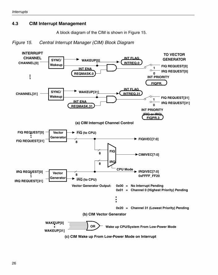
4.3 CIM Interrupt Management
A block diagram of the CIM is shown in Figure 15.
Figure 15. Central Interrupt Manager (CIM) Block Diagram
INTERRUPTCHANNEL
TO VECTORGENERATOR
SYNC/Wakeup
CHANNEL[31] WAKEUP[31]
INT ENA
INTREQ.31INT FLAG
1
0
FIQ REQUEST[31]
IRQ REQUEST[31]
FIQPR.3
INT PRIORITY(FIQ or IRQ)
(a) CIM Interrupt Channel Control
VectorGenerator
FIQ REQUEST[0] FIQ (to CPU)
FIQ
IRQ
(b) CIM Vector Generator
FIQ REQUEST[31]
VectorGenerator
IRQ REQUEST[0]
IRQ REQUEST[31]
8
8
8
CPU Mode
FIQIVEC[7:0]
CIMIVEC[7:0]
IRQIVEC[7:0]0xFFFF_FF20
Vector Generator Output: 0x00 = No Interrupt Pending0x01 = Channel 0 (Highest Priority) Pending
WAKEUP[0]
WAKEUP[31]Wake up CPU/System From Low-Power ModeOR
(c) CIM Wake up From Low-Power Mode on Interrupt
SYNC/WakeupCHANNEL[0]
WAKEUP[0]INTREQ.0INT FLAG
1
0
FIQ REQUEST[0]
IRQ REQUEST[0]
8
0x20 = Channel 31 (Lowest Priority) Pending
FIQPR.
INT PRIORITY
REQMASK.31
INT ENA
REQMASK.0
IRQ (to CPU)
26

Interrupts
The CIM can support 32 interrupt request lines (channel [0] to channel [31])from the peripherals. These peripheral interrupt requests are hardwired toeach of the CIM 32 channels, and these connections are device specific. (Seethe device-specific data sheet for details on which module is tied to whichinterrupt request channel.) All requests pass through a synchronizer toprevent setup time violations; the CIM samples the interrupt requests from thesynchronizer every system clock (SYSCLK) cycle. The CIM combines the32 channels into two outputs – an FIQ request to the CPU and an IRQ requestto the CPU. The CIM performs the following functions:
Manages the input channels Prioritizes the interrupt requests to the CPU
4.3.1 CIM Input Channel Management
On the input side, the CIM enables channels on a channel-by-channel basis(in the REQMASK register); unused channels may be masked to preventspurious interrupts. Each interrupt channel can be designated to send eitheran FIQ or IRQ request to the CPU (in the FIQPR register).
Note: LPM Wake-up Interrupts are not Masked at the CIM
Note that if an interrupt is to be used to wake the device up out of any low-power mode (LPM), the interrupts must be enabled/disabled at the individualmodule level. The REQMASK register has no effect on the enable/disable ofan interrupt while the device is in low-power mode.
4.3.2 CIM Prioritization
The CIM prioritizes the received interrupts based upon a hardware andsoftware prioritization scheme. The software prioritization scheme is userconfigurable. The CIM can send two interrupt requests to the CPUsimultaneously—one IRQ and one FIQ. If both interrupt types are enabled atthe CPU, then the FIQ has greater priority and is handled first. The hardwareprioritization scheme sends the lowest numbered active channel (in each FIQand IRQ interrupt request) to the CPU. Within the FIQ and IRQ classes ofinterrupts, the lowest channel has the highest priority interrupt. The CIMsends the highest priority interrupt (that is, the lowest active channel) of boththe IRQ and FIQ classes of interrupt requests to the CPU.
4.3.3 CIM Operation
When the CPU recognizes an interrupt request and responds, the programcounter jumps to the appropriate interrupt vector. The interrupt vector istypically a branch statement to an interrupt table. The interrupt table reads thepending interrupt from a vector offset register (FIQIVEC.7:0 for FIQ interrupts
System Module (SPNU189H) 27
Interrupts
and IRQIVEC.7:0 for IRQ interrupts). The CIM has an overall offset register(CIMIVEC.7:0) that is read as IRQ offset or FIQ offset depending upon themode of the CPU. (All pending interrupts can be viewed in the INTREQregister.)
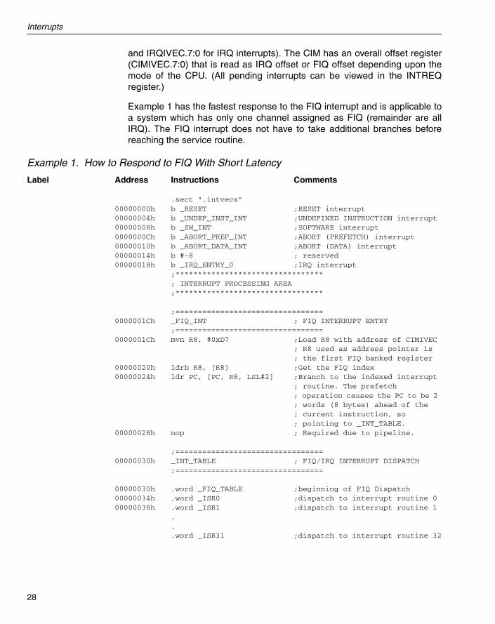
Example 1 has the fastest response to the FIQ interrupt and is applicable toa system which has only one channel assigned as FIQ (remainder are allIRQ). The FIQ interrupt does not have to take additional branches beforereaching the service routine.
Example 1. How to Respond to FIQ With Short Latency
Label Address Instructions Comments
.sect ".intvecs"00000000h b _RESET ;RESET interrupt00000004h b _UNDEF_INST_INT ;UNDEFINED INSTRUCTION interrupt00000008h b _SW_INT ;SOFTWARE interrupt0000000Ch b _ABORT_PREF_INT ;ABORT (PREFETCH) interrupt00000010h b _ABORT_DATA_INT ;ABORT (DATA) interrupt00000014h b #-8 ; reserved00000018h b _IRQ_ENTRY_0 ;IRQ interrupt
;*********************************; INTERRUPT PROCESSING AREA;*********************************
;=================================0000001Ch _FIQ_INT ; FIQ INTERRUPT ENTRY
;=================================0000001Ch mvn R8, #0xD7 ;Load R8 with address of CIMIVEC
; R8 used as address pointer is; the first FIQ banked register
00000020h ldrb R8, [R8] ;Get the FIQ index00000024h ldr PC, [PC, R8, LSL#2] ;Branch to the indexed interrupt
; routine. The prefetch ; operation causes the PC to be 2 ; words (8 bytes) ahead of the ; current instruction, so ; pointing to _INT_TABLE.
00000028h nop ; Required due to pipeline.
;=================================00000030h _INT_TABLE ; FIQ/IRQ INTERRUPT DISPATCH
;=================================
00000030h .word _FIQ_TABLE ;beginning of FIQ Dispatch00000034h .word _ISR0 ;dispatch to interrupt routine 000000038h .word _ISR1 ;dispatch to interrupt routine 1
.
.
.word _ISR31 ;dispatch to interrupt routine 32
28
Interrupts
4.4 System Software Interrupts (SSI)
The TMS470 can initiate an IRQ/FIQ interrupt through software. Theapplication software can initiate an IRQ/FIQ interrupt by writing a specific keyto the system software interrupt request register (SSIR). The most significanteight bits of the SSIR register are the key register bits. When 0x75 is writtento the key register bits, the system software interrupt flag register (SSIF) isset, and an IRQ/FIQ interrupt is generated. The IRQ/FIQ interrupt request isasserted until the software interrupt flag register (SSIF) is cleared by thesoftware. The least significant eight bits of the SSIR register are user registerbits that the application software may use to provide a different entry point forthe system software interrupt routine.
System Module (SPNU189H) 29

Real-Time Interrupt (RTI)
5 Real-Time Interrupt (RTI)
The 470R1x family of microcontrollers provides a real-time interrupt (RTI) thatcan generate interrupts periodically or based on compare values. The RTIruns independently of the software loop or the CPU state (not in halt mode),and provides real time to the system.
5.1 RTI Overview
The primary function of the RTI is to provide a programmable clock period,separate from the system clock domain (RTICLK). (See Section 7, Clocks, onpage 43.)
The RTI may be used for:
Providing periodic interrupts for an operating system
Measuring elapsed time within an application (not necessarily interruptdriven)
Measuring time intervals based upon user/privilege mode forbenchmarking code
The RTI can generate interrupts on three separate channels. There are twoprogrammable compare values and one tap interrupt. The compare valuestrigger an interrupt when the value in the compare control register is equal tothe value in the RTI counter. The tap interrupt, on the other hand, triggers aninterrupt when the selected bit in the counter clears, that is, when the bitchanges from 1 to 0.
5.2 RTI Operating Modes and Conditions
The RTI module is capable of waking up the clock module and bringing thesystem out of idle or low power mode in the same manner as any wake-upinterrupt. Table 6 below lists the different RTI operating modes.
Table 6. RTI Operating Modes
Mode Clocks Analog Watchdog (AWD)
RTI
Run ON - Global RC Digital
Idle ON - Global RC Digital
Standby Local to RTI RC Digital
Halt OFF RC Analog
Test ON Reset disabled Interrupt disabled
30

Real-Time Interrupt (RTI)
The DRTI operates in run, idle and standby modes. The AWD operates at alltimes except during test mode. In test mode, the AWD should not be allowedto reset the device. This can be handled by controlling the capacitance levelon the external AWD pin.
5.2.1 RTI Module Clock Source
A dedicated clock, RTICLK, is used by the RTI module to clock its internalcounters. This RTICLK comes from the clock control module (CCM). RTICLKcan have two different sources - the oscillator clock coming directly from theoscillator or the clock coming from the on chip phase lock loop (PLL). Theregister bit RTI OSC EN (GLBCTRL.14) of the System Module Global ControlRegisters is used to select the clock source. There is also the option ofenabling or disabling the on-chip PLL. The register bit PLL STBY DIS(GLBCTRL.13) of the System Module Global Control Register handles thisfeature. This is an added feature to some devices and will be denoted as theEnhanced RTI Module (See the device-specific data sheet to see if thisfeature has been implemented).
Once RTI OSC EN is programmed, the source of RTICLK is the oscillator forall operating modes. When PLL STBY DIS is programmed, the PLL isdisabled upon entering STBY mode. This results in lower currentconsumption. When the device is awakened from STBY mode, the PLL willrelock. An external interrupt to the CIM/IEM will trigger the PLL to start therelock process. While the PLL relocks, the system clocks are held off for 4096cycles. See Table 7 for the clocks available to the RTI module and thecorresponding PLL activities during standby mode.
Table 7. PLL State During Standby Mode
5.3 RTI Operation
A block diagram of the RTI is shown in Figure 16.
RTI OSC EN PLL STBY DISRTI Clock
Source PLL ON/OFF
0 0 PLL CLOCK ON
0 1 PLL CLOCK ON
1 0 OSC CLOCK ON
1 1 OSC CLOCK OFF
System Module (SPNU189H) 31

Real-T
ime Interrupt (R
TI)
32
0:0
0:0
CF2
CF1
To CIM
RTIE
CE2
CE1
To CIM
To CIM
Compare 2flag
Compare 1flag
Figure 16. RTI Block Diagram
CNTEN.1:0
CPU mode
PRELD.10:0
Preload
Prescale
MOD.10:0
RTICLK
CNTR.20:0
Counter
Tap
RTIM.2:0
COMPARE2.2
Compare 2
Compare 1
COMPARE1.2
Tap flag
RTIF

Real-Time Interrupt (RTI)
The RTI is clocked by the RTICLK, which runs at SYSCLK frequency (seeSection 7, Clocks, on page 43). The RTI counts RTICLK periods based uponthe state of the CPU and the control bits CNTEN.1:0 (RTICNTEN.1:0). An11-bit preload value, PRELD.10:0 (RTIPCTL.10:0), provides the prescalevalue. The prescale, MOD.10:0 (RTICNTR.10:0) counts down from thepreload to 0.
When the prescale counts down to 0, a 21-bit counter is incremented. Thecounter, CNTR.20:0 (RTICNTR.31:11), is a count up counter. During a readaccess, both of the RTI counters (MOD.10:0 and CNTR.20:0) are readtogether in the same cycle as a single 32-bit value (RTICNTR.31:0). However,because the modulo M counter (MOD.10:0) is a down counter, a calculationneeds to be performed to convert the 32-bit RTI counter value into systemclock cycles which is given by Equation 1:
(EQ 1)
Where:
M = Preload value PRELD.10:0 (RTIPCL.10:0), when PRELD.10:0 = 0, M = 2048
m = Current value of MOD.10:0 (RTICNTR.10:0)
N = Current value of CNTR.20:0 (RTICNTR.31:11)
The real-time counter can generate three distinct interrupts off of this upcounter:
Tap interrupt Two compare interrupts (Compare1 and Compare 2)
5.3.1 Tap Interrupt
The tap interrupt is configured so that when a specified bit of the counter iscleared, the tap interrupt is generated. The RTIM.2:0 bit field(RTIPCTL.13:11) designates which bit is tapped for the interrupt. (See Table8 for relationship between RTIM.2:0 bits and tap value.) This tap interrupt flag,RTIF (RTICNTL.7), is set every time the specific bit transitions from 1 to 0. Inorder to generate an interrupt, the tap interrupt enable, RTIE (RTICNTL.6),must be set; the tap interrupt is periodic.
Note: Clear Tap Flag Before Enabling Interrupt
Prior to enabling the tap interrupt, the interrupt flag should be cleared toprevent spurious interrupts.
RTIClockCycles M 1+( )xN M nm–( )+=
System Module (SPNU189H) 33

Real-Time Interrupt (RTI)
Table 8. Tap Interrupts
The tap interrupt is calculated as shown in Equation 2:
(EQ 2)
Where:
M = Preload value PRELD.10:0 (RTIPCL.10:0), when PRELD.10:0 = 0, M = 2048.
TapValue is the value shown in Table 8.
T = Tap Period
Tap period assumes that CNTEN.1:0 (RTICNTEN.1:0) = 0x00
5.3.2 Compare Interrupts
The compare interrupt flags, CF1 (RTICINT.7) or CF2 (RTICINT.6), are setwhen the 21-bit compare value, COMPARE1.20:0 (RTICMP1.20:0) orCOMPARE2.20:0 (RTICMP2.20:0), is equal to the 21-bit counter value. Inorder to generate an interrupt, the compare interrupt enable, CE1(RTICINT.5) or CE2 (RTICINT.4) must be set.
RTIM.2:0(Binary)
Tap Bit
Tap Value
000 CNTR.20 RTICNTR.31 2097152
001 CNTR.17 RTICNTR.28 262144
010 CNTR.14 RTICNTR.25 32768
011 CNTR.11 RTICNTR.22 4096
100 CNTR.8 RTICNTR.19 512
101 CNTR.5 RTICNTR.16 64
110 CNTR.2 RTICNTR.13 8
111 Underflow Underflow 1
T M 1+( ) TapValue( ) RTICLKPeriod( )××=
34

Real-Time Interrupt (RTI)
Note: Clear Compare Flag Before Enabling Interrupt
Before the compare interrupt is enabled, the interrupt flag should be clearedto prevent spurious interrupts.
5.4 Analog Watchdog
The 470R1x family of devices may have an external AWD pin. This pin hasan internal pull-down so that when the pin is unconnected, the analogwatchdog is disabled. When an RC combination is added to the AWD pin, thevoltage level on the pin depends on the specific value of resistor andcapacitor.
Figure 17. External Required Circuit for Watchdog
When the voltage passes Vth (see device specification for Vth on AWD), theanalog watchdog generates a system reset. The watchdog reset is caused bya high voltage level on the AWD pin.
The watchdog may be cleared by writing 0x0E5 and then 0x0A3 to the WKEYregister. When the correct values are written, the analog watchdog drains theexternal capacitor and resets the external RC delay. If an incorrect value iswritten to the WKEY register, a watchdog reset occurs immediately. Table 9illustrates the WKEY register sequence.
VCCIO
RDS
R
Pull-down
AWD
Output buffercan drive low;cannot drive high
C
System Module (SPNU189H) 35

Real-Time Interrupt (RTI)
In applications using the analog watchdog (AWD) pin, the choice of externalresistor (R), external capacitor (C), and watchdog discharge time(TWATCHDOG) must be chosen in order to include the interaction with thesilicon. The AWD pin must be tied to ground if not used. In most cases, theAWD pin has an on-silicon pull-down, implemented with a current source toground, so that the pin is not required to be connected externally. (If there isno pull-down, the AWD must be tied to ground externally in order to preventAWD resets.) When the AWD key is written, the output buffer sinks current for256 SYSCLK cycles in order to discharge the external capacitor. Thepresence/absence of a pull-down, its current range, and the size of the outputbuffer are device-specific and must be verified against the device data sheet.
Figure 17 shows a system configuration with external resistor and capacitor.It shows that the AWD resistor, capacitor and discharge interval are:
AWD threshold (min and max)
VCCIO (min and max)
Pull-down current (min and max)
Maximum drain-source resistance for the output buffer when enabled(RDSON)
Table 9. Example WKEY Register Sequence
StepValue Writtento WKEY Result
1 0x0A3 No action
2 0x0A3 No action
3 0x0E5 WKEY is enabled for reset by the next 0x0A3.
4 0x0E5 WKEY is enabled for reset by the next 0x0A3.
5 0x0E5 WKEY is enabled for reset by the next 0x0A3.
6 0x0A3 Watchdog is reset.
7 0x0A3 No action
8 0x0E5 WKEY is enabled for reset by the next 0x0A3.
9 0x0A3 Watchdog is reset.
10 0x0E5 WKEY is enabled for reset by the next 0x0A3.
11 0x023 System reset due to an improper key value written to WKEY.
36

Real-Time Interrupt (RTI)
SYSCLK frequency [discharge is active for 256 cycles]
5.4.1 AWD Threshold
Figure 18. AWD Threshold
The external resistor and capacitor values need to be chosen so that theAWD will trip and generate a reset if not discharged. (Note that the AWD whennot used is configured so that it cannot trip and generate a reset.) Specifically,the hardware must allow the voltage on the AWD pin to exceed AWDthreshold (max) in order to guarantee a reset on all parts over the specifiedvoltage and temperature ranges.
At the same time, the discharge interval must be chosen so that the voltageon the AWD pin never reaches the minimum AWD threshold. The softwaremust discharge the capacitor while the AWD is guaranteed not to trip andgenerate a reset.
When the voltage is greater than the minimum AWD threshold and less thanthe maximum AWD threshold, the AWD will trip on some devices but not all.For the sake of figuring the discharge interval, this region must be completelyavoided.
5.4.2 Effect of Pull-down
The pull-down has the effect of lowering the charging asymptote by I(Pull-
down)R as seen in Figure 19.
AWD guaranteed not to trip
AWD threshold (max)
AWD guaranteed to trip
Time
Vol
tage
AWD threshold (min)
System Module (SPNU189H) 37

Real-Time Interrupt (RTI)
Figure 19. Effect of Pull-down
As the discharge time is fixed by SYSCLK, the capacitor may not dischargefully. If not fully discharged, each charge/discharge cycle will start from a newvoltage level until the discharging voltage equals the charging voltage, asshown in Figure 20. At this point, the charging starts from some voltage V0,charges to VF, and is discharged back to V0.
1.00E+00
9.00E-01
8.00E-01
7.00E-01
6.00E-01
5.00E-01
4.00E-01
3.00E-01
2.00E-01
1.00E-01
0.00E+00
0.00E+001.00E+00
2.00E+003.00E+00
4.00E+005.00E+00
6.00E+007.00E+00
8.00E+009.00E+00
1.00E+01
Time (time constants)
% o
f VC
CIO
V = VCCIO - I(Pull-down)R
38

Real-Time Interrupt (RTI)
Figure 20. Sequential AWD Charge/Discharge Cycles Reach Charge Asymptote
5.4.3 Effect of RDSON
The output buffer has a resistance from drain to source. The maximumresistance is determined by the buffer strength, as shown in Table 10. Pleasesee the device-specific data sheet.
Table 10. Maximum Resistance by Buffer Strength
The non-zero value of RDSON means that the capacitor discharge follows anRC discharge curve, as shown in Table 11.
Buffer RDSON (max)
2 mA 150 Ω
4 mA 75 Ω
8 mA 38 Ω
System Module (SPNU189H) 39

Real-Time Interrupt (RTI)
Table 11. RC Discharge Curve
The discharge time may not be sufficient to discharge the AWD pin all the wayto ground. In this case, some residual charge remains on the capacitor andthe next charging cycle begins from the voltage to which the capacitor wasdischarged.
The resistor, capacitor, discharge interval must be chosen so that the AWDnever trips – guaranteeing that the pin does not trip during the first charge/discharge cycle is not sufficient.
Capacitance Resistance Time
Charging C RTWATCHDOG - 256*TSYSCLK
Discharging C RDSON 256*TSYSCLK
40

Resets
6 Resets
The TMS470R1x device generates a reset in response to multiple causes.Table 12 shows the different resets and their cause.
Table 12. Causes of TMS470R1x Reset/Abort
Reset Cause
Power-On Reset (PORRST)
The voltage on the PORRST pin is low. A reset occurs when an external voltage moni-tor pulled PORRST pin low. A power on reset indicates an initial power up or a voltage supply dip.
Flag: SYSESR.15
Clock
A clock reset indicates that the external oscillator’s frequency is too low or that the PLL has detected a discrepancy between the reference and VCO phase. See the device specific data sheet for the frequency value that triggers the OSC FAIL flag (f(OSCRST)). A reset occurs if:
1. PLL slip (GLBSTAT.0) = 1 or2. RST OSC FAIL (GLBCTRL.15) = 1 and OSC FAIL (GLBSTAT.1) = 1
Watchdog
A watchdog reset indicates that the watchdog counter was not reset prior to the AWD pin reaching its threshold voltage.
Flag: SYSESR.13
See Section 5.1, RTI Overview, on page 30 for further details.
Illegal Mode
An illegal mode reset indicates that the ARM mode bits in the current program status register (CPSR) are not in one of the seven legal modes (user, FIQ, IRQ, supervisor, abort, undefined, or system).
Flag: SYSESR.12
Illegal Address
(1) An illegal address reset/abort indicates an access to an unimplemented address in the memory. The illegal address reset/abort is generated by the system.
(2) The memory protection unit (MPU) may generate an illegal address reset/abort if the memory access within the memory select is not within one of the MPU selects.
• An illegal address generates an abort in user mode.
• An illegal address generates a reset in privilege mode.
See Section 3.4.1, Illegal Address, on page 22 for more information.
System Module (SPNU189H) 41

Resets
Illegal Access
An illegal access reset/abort indicates:
(1) a write access to protected memory; or
(2) an access to a memory location when in user mode.
The illegal access reset/abort is generated by the system or the memory protection unit (MPU).
• Illegal access generates an abort in user mode.
• Illegal access generates a reset in privilege mode.
See Section 3, Memory, on page 14 for more information.
Peripheral Ille-gal Access
A peripheral illegal access abort indicates an access to a protected peripheral when in user mode. The peripheral protection register (PPROT) allows the user to restrict access to peripherals when in user mode.
• A peripheral illegal access generates an abort in user mode.
See Section 3, Memory, on page 14 for more details.
Illegal Map
An illegal map reset indicates an access to overlapped memory regions. The address decoder (DEC) does not prevent the user from overlapping memory regions; when the overlapped region is accessed, the reset occurs.
See Section 3, Memory, on page 14 for more details.
Software ResetA software reset is triggered by a write to SYSECR.15:14. SYSECR.15 = 0 and SYSECR.14 = 1 does not generate a reset.
External Reset (RST)
The external reset is generated when the RST pin is driven low.
Table 12. Causes of TMS470R1x Reset/Abort (Continued)
Reset Cause
42

Clocks
7 Clocks
The TMS470R1x has five separate clock domains. Table 13 describes theclock domains.
The clock domains are active/inactive in different device modes. Table 14summarizes the clock domain activity based on device conditions.
Table 13. Clock Domains
Clock Description
ACLKACLK is the output clock from the oscillator/PLL prior to the prescale divider. The system synthesizes the other device clocks off the prescaled ACLK.
SYSCLK
The clock control module synthesizes SYSCLK from ACLK by dividing the frequency by the prescale divider (GLBCTRL). SYSCLK clocks:
RAMHETFlash control registersFlashSystem control registersDMA
MCLKMCLK operates at the same frequency as SYSCLK and is inverted (180° out of phase). MCLK clocks the CPU.
ICLKICLK is generated from the SYSCLK, and the frequency is controlled by a prescale (PCR.4:1). ICLK clocks peripherals.
RTICLKRTICLK operates at the same frequency and is in phase with the SYSCLK. RTICLK clocks only the real-time interrupt counters.
System Module (SPNU189H) 43

Clocks
Table 14. Active Clock Domains and Device Condition
7.1 Low-Power ModesMembers of the TMS470R1x family of devices have two low-power modes(halt and standby) and an idle mode. The low power modes reduce theoperating power by reducing or stopping the activity of various modules. Bits0 and 1 of the clock control register (CLKCNTL) select the halt, standby, oridle modes.
The standby mode stops the system clocks. The RTI clock is still active. Adevice can be awakened from standby mode by the following events:
RTI interrupt External interrupt CAN message Class II message SCI message I2C message
The halt mode stops the internal clock. This stops processing in all of themodules, resulting in the lowest amount of power consumption. A device canbe awakened from halt by any of the following events:
External interrupt CAN message Class II message SCI message I2C message
Device Condition LPM Bits Oscillator ACLK RTICLK SYSCLK ICLK MCLK
RUNLPM.1:0 = 0x00
Active Active Active Active Active Active
RST low n/a Active Active Active Active Active Active
IDLELPM.1:0 = 0x01
Active Active Active Active Active Inactive
STAND-BY
LPM.1:0 = 0x02
Active Active Active Inactive Inactive Inactive
PORRST low
n/a Active InactiveInac-tive
Inactive Inactive Inactive
HALTLPM.1:0 = 0x03
Inactive InactiveInac-tive
Inactive Inactive Inactive
44

Clocks
The idle mode (which is not a low-power mode) is a state that waits for thenext interrupt. A device can be awakened from idle by any interrupt.
When a device is initially powered or when it is coming out of a low-powermode, there is an associated delay that exists before code execution canbegin. This delay permits the PLL to lock. The following formulas provide thelength of the delay.
a) From Power Down = regulator ramp/oscillator start time + 4096OSCIN cycles + 8 SYSCLK cycles(Regulator ramp/oscillator start time is application dependent.)
b) From Halt = oscillator start time + 4096 OSCIN cycles + # of cyclesrequired to service the interrupt(Oscillator start time is the time it takes to start oscillations.)
c) From Standby w/ PLL disabled = 4096 OSCIN cycles + # of cyclesrequired to service the interrupt(Oscillator is active during Standby mode.)
d) From Standby w/ PLL enabled = "any analog delay" + # of cyclesrequired to service the interrupt(When PLL is active, system clocks are not held off for 4096 cycles.)
System Module (SPNU189H) 45

Parallel Signature Analyzer Overview
8 Parallel Signature Analyzer Overview
The PSA produces a signature for a given sequence of CPU data bus values.The signature is generated through a feedback path from data bus bits 0, 1,2, 22, and 31. (See Figure 21.) The PSA signature is based on the primitivepolynomial in Equation 3.
f(X) = 1 + X + X2 + X22 + X31 (EQ 3)
Figure 21. PSA Operation
Identical bus sequences produce identical signatures when the PSA isinitialized with the same seed value, whereas different sequences of busactivity generally produce different signatures.
The PSA is first initialized by writing a seed value to CPUPSA. The PSA thenmonitors the CPU data bus and generates a signature value.
One common application of the PSA is to verify the contents of the on-chipmemories, either in test or functional modes. This is accomplished byinitializing the PSA to a known seed value, using a quick instruction loop toread from the memory, and verifying the PSA signature at the end of the loop.Other applications include online testing.
8.1 PSA Updates
A PSA update is defined as compression of one data bus word. To achieveconsistent signatures, the PSA updates during every CPU read data accessfrom memory. The PSA does not update during instruction fetches. Since onlyCPU memory read accesses trigger PSA updates, differences in memorylatencies from the memory subsystem are ignored. In addition, DMA memoryaccesses do not affect the PSA signature. Furthermore, for accesses of lessthan a word (32-bits), the PSA treats the non-valid bits of the CPU bus aszeros. After a device reset, the PSA reverts to its initial value and startsupdating on the first CPU memory access.
0 1 2 3 4 5 6 22 23 24 25 31
D(31:0)
46

Parallel Signature Analyzer Overview
8.2 Read/Write Operation
When the PSA register is read, the PSA returns the current signature to thedata bus. The PSA then updates after the CPU data’s next memory access.When the PSA register is written with the seed value, the register startsupdating after the next CPU memory access. Depending on the size of thedata access (word, half-word or byte), the PSA reads in the appropriate datasize from the CPU data bus and treats the remaining bits on the data bus aszeros. The PSA does not update during a wait state or system reset.
8.3 Emulation Support
In emulation mode, the PSA does not perform any updates. This allowsinterrupted code to behave correctly when continued.
8.4 Enable/Disable
The PSA can be turned on or off to conserve power. To power down the PSA,a 1 must be loaded into the PSADIS. When powered down, the PSA stopsfunctioning and the current status of the registers remains the same. The PSAis powered on by a 0 being written to the PSADIS bit.
Note:
There is a small probability that signature aliasing can occur for differentsequences and result in identical signatures. In this case, any fault isundetected.
8.5 PSA Pseudo Code
The PSA pseudo code in shown in Example 2.
Example 2. PSA Pseudo Code
union ubits unsigned int uint;
struct unsigned char by0;
unsigned char by1;unsigned char by2;unsigned char by3;
bytes;struct int b0:1;
int b1:1;int b2:1;int:18;
System Module (SPNU189H) 47

Parallel Signature Analyzer Overview
int b21:1;int b22:1;int:8;int b31:1;
bits;;
UNIT32 calc_psa (UNIT32 *data, Unit32 length, UNIT32 seed) union ubits a,b,c;
UNIT32 i;c.uint-seedfor (i=0;i<length>2;i++) a.uint=data[1];
b.bytes.by0=a.bytes.by3;b.bytes.by1=a.bytes.by2;b.bytes.by2=a.bytes.by1;b.bytes.by3=a.bytes.by0;a.uint=c.uint;
c.uint=b.uint^(a.uint<<1);c.bits.b0=a.b31^b.bits.b0;c.bits.b1=b.bits.b1^a.bits.b0^a.bits.b31;c.bits.b2=b.bits.b2^a.bits.b1^a.bits.b31;c.bits.b22=b.bits.b22^a.bits.b21^a.bits.b31;
return c.uint;
48

Registers
9 Registers
This section details the system module registers memory map as listed inTable 16. A detailed description of each register and its bits is also provided.
Each register begins on a word boundary. The registers in Table 16 are listedin address order with the MPU registers listed first. For architectures with470+, all system register accesses take two cycles; for architectures otherthan 470+, system register accesses take one cycle.
The registers within the system module have either 16-bit or 32-bit accesssizes as shown in Table 15. No register is accessible for 8-bit writes.
Table 15. System Register Accessibility
32-BIT ACCESSES ONLY 16-BIT or 32-BIT ACCESSES
MPUA(H/L)Rx SMCRx
MPUCTRL WCR0
RTICNTR PCR
RTIPCTL PLR
RTICNTL PPROT
WKEY MFBA(H/L)Rx
RTICMP1 MCBA(H/L)Rx
RTICMP2 CLKCNTL
RTICINT GLBCTRL
RTICNTEN SYSECR
IRQIVEC SYSESR
FIQIVEC ABRTESR
CIMIVEC GLBSTAT
FIRQPR DEV
INTREQ SSIF
REQMASK SSIR
CPUPSA
PSAENABLE
System Module (SPNU189H) 49

Registers
50 Table 16. Control Register Map Offset Address
Register31 15
30 14
29 13
28 12
27 11
26 10
25 9
24 8
23 7
22 6
21 5
20 4
19 3
18 2
17 1
16 0 Page
Memory Protection Unit (Addresses are pointers)
0x0066
EQUAL 66
66
EQUAL 66
66
MPUAHR0Reserved
UPPERBOUND
0x04
MPUALR0Reserved
LOWERBOUND
0x08
MPUAHR1Reserved
UPPERBOUND
0x0C
MPUALR1Reserved
LOWERBOUND
0x10
MPUAHR2Reserved
UPPERBOUND

Registers
Offset Address Register
31 15
30 14
29 13
28 12
27 11
26 10
25 9
24 8
23 7
22 6
21 5
20 4
19 3
18 2
17 1
16 0 Page
EQUAL 66
66
EQUAL 66
67
CHAN0RONLY
CHAN0PRIV
CHAN0EN
CHAN0Special
71
END Rsrv’d DW
Table 16. Control Register Map (Continued)
System
Module (S
PN
U189G
)51
0x14
MPUALR2Reserved
LOWERBOUND
0x18
MPUAHR3Reserved
UPPERBOUND
0x1C
MPUALR3Reserved
LOWERBOUND
0x20
MPUCTRLReserved
CHAN3RONLY
CHAN3PRIV
CHAN3EN
CHAN3Special
CHAN2RONLY
CHAN2PRIV
CHAN2EN
CHAN2Special
CHAN1RONLY
CHAN1PRIV
CHAN1EN
CHAN1Special
Static Control Registers
0xFFFF_FD00
SMCR0Reserved
Reserved ASC TWS Rsrv’d WS

Registers
52
Offset Address Register
31 15
30 14
29 13
28 12
27 11
26 10
25 9
24 8
23 7
22 6
21 5
20 4
19 3
18 2
17 1
16 0 Page
0xFFFF_FD04Reserved 74
END MLOC DW
74
END MLOC DW
74
END MLOC DW
74
END MLOC DW
74
END MLOC DW
Table 16. Control Register Map (Continued)
SMCR1
Reserved ASC TWS Rsrv’d WS
0xFFFF_FD08
SMCR2Reserved
Reserved ASC TWS Rsrv’d WS
0xFFFF_FD0C
SMCR3Reserved
Reserved ASC TWS Rsrv’d WS
0xFFFF_FD10
SMCR4Reserved
Reserved ASC TWS Rsrv’d WS
0xFFFF_FD14
SMCR5Reserved
Reserved ASC TWS Rsrv’d WS

Registers
Offset Address Register
31 15
30 14
29 13
28 12
27 11
26 10
25 9
24 8
23 7
22 6
21 5
20 4
19 3
18 2
17 1
16 0 Page
74
END MLOC DW
74
END MLOC DW
74
END MLOC DW
74
END MLOC DW
75
WTWSOVR
WBEN
ABLE
Table 16. Control Register Map (Continued)
System
Module (S
PN
U189G
)53
0xFFFF_FD18
SMCR6Reserved
Reserved ASC TWS Rsrv’d WS
0xFFFF_FD1C
SMCR7Reserved
Reserved ASC TWS Rsrv’d WS
0xFFFF_FD20
SMCR8Reserved
Reserved ASC TWS Rsrv’d WS
0xFFFF_FD24
SMCR9Reserved
Reserved ASC TWS Rsrv’d WS
0xFFFF_FD2C
WCR0Reserved
Reserved

Registers
54
Offset Address Register
31 15
30 14
29 13
28 12
27 11
26 10
25 9
24 8
23 7
22 6
21 5
20 4
19 3
18 2
17 1
16 0 Page
0xFFFF_FD30Reserved 76
CLKDIV PENABLE
78
79
81
81
0 Rsrv’d RONLY PRIV
Table 16. Control Register Map (Continued)
PCR
Reserved
0xFFFF_FD34
PLRReserved
PLOC.15:0
0xFFFF_FD38
PPROTReserved
PPROT.15:0
Memory Fine Base Address Registers
0xFFFF_FE00
MFBAHR0Reserved
Address.31:16
0xFFFF_FE04
MFBALR0Reserved
Address.15:10 Rsrv’d MS Block Size

Registers
Offset Address Register
31 15
30 14
29 13
28 12
27 11
26 10
25 9
24 8
23 7
22 6
21 5
20 4
19 3
18 2
17 1
16 0 Page
84
84
Reserved RONLY PRIV
84
84
Reserved RONLY PRIV
84
Table 16. Control Register Map (Continued)
System
Module (S
PN
U189G
)55
0xFFFF_FE08
MFBAHR1Reserved
Address.31:16
0xFFFF_FE0C
MFBALR1Reserved
Address.15:10 AW Rsrv’d Block Size
0xFFFF_FE10
MFBAHR2Reserved
Address.31:16
0xFFFF_FE14
MFBALR2Reserved
Address.15:10 AW Rsrv’d Block Size
0xFFFF_FE18
MFBAHR3Reserved
Address.31:16

Registers
56
Offset Address Register
31 15
30 14
29 13
28 12
27 11
26 10
25 9
24 8
23 7
22 6
21 5
20 4
19 3
18 2
17 1
16 0 Page
0xFFFF_FE1CReserved 84
Reserved RONLY PRIV
84
84
Reserved RONLY PRIV
84
84
Reserved RONLY PRIV
Table 16. Control Register Map (Continued)
MFBALR3
Address.15:10 AW Rsrv’d Block Size
0xFFFF_FE20
MFBAHR4Reserved
Address.31:16
0xFFFF_FE24
MFBALR4Reserved
Address.15:10 AW Rsrv’d Block Size
0xFFFF_FE28
MFBAHR5Reserved
Address.31:16
0xFFFF_FE2C
MFBALR5Reserved
Address.15:10 AW Rsrv’d Block Size

Registers
Offset Address Register
31 15
30 14
29 13
28 12
27 11
26 10
25 9
24 8
23 7
22 6
21 5
20 4
19 3
18 2
17 1
16 0 Page
86
86
0 Rsrv’d RONLY PRIV
86
86
0 Rsrv’d RONLY PRIV
86
Table 16. Control Register Map (Continued)
System
Module (S
PN
U189G
)57
0xFFFF_FE30
MCBAHR0Reserved
Address.31:16
0xFFFF_FE34
MCBALR0Reserved
Address.15 Reserved AW Rsrv’d Block Size
0xFFFF_FE38
MCBAHR1Reserved
Address.31:16
0xFFFF_FE3C
MCBALR1Reserved
Address.15 Reserved AW Rsrv’d Block Size
0xFFFF_FE40
MCBAHR2Reserved
Address.31:16

Registers
58
Offset Address Register
31 15
30 14
29 13
28 12
27 11
26 10
25 9
24 8
23 7
22 6
21 5
20 4
19 3
18 2
17 1
16 0 Page
0xFFFF_FE44Reserved 86
0 Rsrv’d RONLY PRIV
86
86
0 Rsrv’d RONLY PRIV
86
86
0 Rsrv’d RONLY PRIV
Table 16. Control Register Map (Continued)
MCBALR2
Address.15 Reserved AW Rsrv’d Block Size
0xFFFF_FE48
MCBAHR3Reserved
Address.31:16
0xFFFF_FE4C
MCBALR3Reserved
Address.15 Reserved AW Rsrv’d Block Size
0xFFFF_FE50
MCBAHR4Reserved
Address.31:16
0xFFFF_FE54
MCBALR4Reserved
Address.15 Reserved AW Rsrv’d Block Size

Registers
Offset Address Register
31 15
30 14
29 13
28 12
27 11
26 10
25 9
24 8
23 7
22 6
21 5
20 4
19 3
18 2
17 1
16 0 Page
86
86
0 Rsrv’d RONLY PRIV
89
90
92
Reserved
Table 16. Control Register Map (Continued)
System
Module (S
PN
U189G
)59
0xFFFF_FE58
MCBAHR5Reserved
Address.31:16
0xFFFF_FE5C
MCBALR5Reserved
Address.15 Reserved AW Rsrv’d Block Size
0xFFFF_FF00
RTICNTRCNTR.20:5
CNTR.4:0 MOD.10:0
0xFFFF_FF04
RTIPCTLReserved
Reserved RTIM.2:0 PRELD.10:0
0xFFFF_FF08
RTICNTLReserved
Reserved TAPFLAG
TAPENA

Registers
60
Offset Address Register
31 15
30 14
29 13
28 12
27 11
26 10
25 9
24 8
23 7
22 6
21 5
20 4
19 3
18 2
17 1
16 0 Page
0xFFFF_FF0CWKEY.31:16 93
COMPARE1.20:16 94
COMPARE2.20:16 94
95
CMP2ENA Reserved
97
CNTEN.1:0
Table 16. Control Register Map (Continued)
WKEY
WKEY.15:0
0xFFFF_FF10
RTICMP1Reserved
COMPARE1.15:0
0xFFFF_FF14
RTICMP2
COMPARE2.15:0
0xFFFF_FF18
RTICINTReserved
Reserved CMP1FLAG
CMP2FLAG
CMP1ENA
0xFFFF_FF1C
RTICNTENReserved
Reserved

Registers
Offset Address Register
31 15
30 14
29 13
28 12
27 11
26 10
25 9
24 8
23 7
22 6
21 5
20 4
19 3
18 2
17 1
16 0 Page
98
EC.7:0
99
D.7:0
100
C.7:0
101
101
Table 16. Control Register Map (Continued)
System
Module (S
PN
U189G
)61
0xFFFF_FF20
IRQIVECReserved
Reserved IRQIV
0xFFFF_FF24
FIQIVECReserved
Reserved FIQIVE
0xFFFF_FF28
CIMIVECReserved
Reserved CIMVE
0xFFFF_FF2c
FIRQPRFIRQPR.31:16
FIRQPR.15:0
0xFFFF_FF30
INTREQINTREQ.31:16
INTREQ.15:0

Registers
62
Offset Address Register
31 15
30 14
29 13
28 12
27 11
26 10
25 9
24 8
23 7
22 6
21 5
20 4
19 3
18 2
17 1
16 0 Page
0xFFFF_FF34REQMASK.31:16 102
103
103
PSADIS
105
CLKDIR
CLKDOUT
CLKDIN LPM
108
FLCON-FIG
PLL Specific
Table 16. Control Register Map (Continued)
REQMASK
REQMASK.15:0
0xFFFF_FF40
CPUPSACPUPSA.31:16
CPUPSA.15:0
0xFFFF_FF50
PSAENABLEReserved
Reserved
0xFFFF_FFD0
CLKCNTLReserved
Reserved PPWNOVR CLKSR
0xFFFF_FFDC
GLBCTRLReserved
PLLSpecific
RTIOSCEN
PLLSTBYDIS
PLL Specific

Registers
Offset Address Register
31 15
30 14
29 13
28 12
27 11
26 10
25 9
24 8
23 7
22 6
21 5
20 4
19 3
18 2
17 1
16 0 Page
110
PACCOVR
ACCOVR
ILLOVR
112
Reserved
115
116
Reserved OSCFAIL
PLLSLIP
119
Table 16. Control Register Map (Continued)
System
Module (S
PN
U189G
)63
0xFFFF_FFE0
SYSECRReserved
RESET RESET Reserved
0xFFFF_FFE4
SYSESRReserved
PORRST
CLKRST
WDRST
ILLMODE
ILLADR
ILLACC
PLLACC
ILLMAP
SWRST
0xFFFF_FFE8
ABRTESRReserved
ADRABT
MEMABT
PACCVIO Reserved
0xFFFF_FFEC
GLBSTATReserved
Reserved SYSADDR
SYSACC
MPUADDR
MPUACC
0xFFFF_FFF0
DEVReserved
DEV.15:0

Registers
64
Offset Address Register
31 15
30 14
29 13
28 12
27 11
26 10
25 9
24 8
23 7
22 6
21 5
20 4
19 3
18 2
17 1
16 0 Page
0xFFFF_FFF8Reserved 120
SSIFLAG
121
SSDATA.7:0
Table 16. Control Register Map (Continued)
SSIF
Reserved
0xFFFF_FFFC
SSIRReserved
SSKEY.7:0

Registers
9.1 MPU Address Registers
This section describes all MPU address registers used to define any memorysub-regions that require protection checks. The MPU contains eight addressregisters, two for each channel, as shown in Table 17. It should be noted thatthe MPU upper and lower bound address registers need to be written to byfirst right-rotating the value by two bits.
Figure 22 illustrates the MPU register alignment with the address bus.
Figure 22. MPU Register Alignment with Address Bus
1) If the address on the address bus is less than LOWERBOUND, the MPUchannel cannot allow access to the region.
2) If the address on the address bus is greater than LOWERBOUND and ifthe address on the address bus is bounded by UPPERBOUND andEQUAL, then the MPU channel allows access to the address based uponthe protection specified in MPUCTRL.
Table 17. MPU Registers
Register Offset Address
MPUAHR0 0x00
MPUALR0 0x04
MPUAHR1 0x08
MPUALR1 0x0C
MPUAHR2 0x10
MPUALR2 0x14
MPUAHR3 0x18
MPUALR3 0x1C
MPUCTRL 0x20
Address Bus
15 0
17 2
15 0
1:0
=
≤
≤
MPUAHR
MPUALR
20:18
18:16
System Module (SPNU189H) 65

Registers
9.1.1 MPU Address High Register (MPUAHRx)
Bits [31:16] Reserved.
Reads are undefined and writes have no effect.
Bits [15:0] UPPERBOUND. UPPERBOUND defines the upper bound of the memory region protected bythe MPU channel. The address bus (shifted right by 2) is compared toUPPERBOUND.
9.1.2 MPU Address Low Register (MPUALRx)
Bits [31:1] Reserved.
Reads are undefined and writes have no effect.
Bits [18:16] EQUAL.
Address bus bits 20:18 are compared to EQUAL.
Bits [15:0] LOWERBOUND.
Bits 31 30 29 28 27 26 25 24 23 22 21 20 19 18 17 16
Offset0x00 Reserved
Bits 15 14 13 12 11 10 9 8 7 6 5 4 3 2 1 0
UPPERBOUND
RWP-0
R = Read in all modes, WP = Write in privilege mode only; -n = Value after reset
Bits 31 30 29 28 27 26 25 24 23 22 21 20 19 18 17 16
Offset_0x04 Reserved EQUAL
R-0 RWP-0
Bits 15 14 13 12 11 10 9 8 7 6 5 4 3 2 1 0
LOWERBOUND
RWP-0
RWP = Read in all modes, write in privilege mode only; -n = Value after reset
66
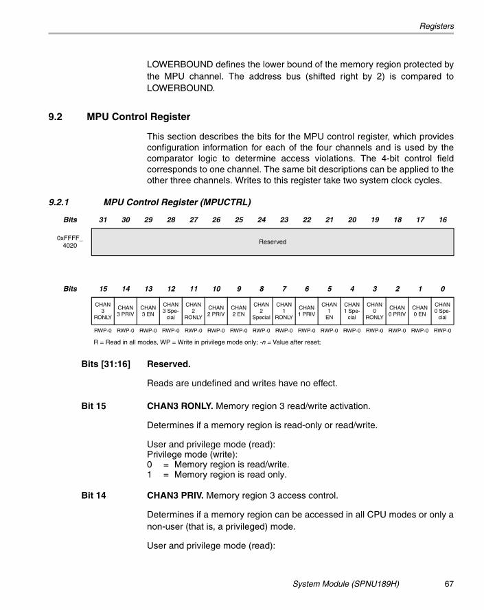
Registers
LOWERBOUND defines the lower bound of the memory region protected bythe MPU channel. The address bus (shifted right by 2) is compared toLOWERBOUND.
9.2 MPU Control Register
This section describes the bits for the MPU control register, which providesconfiguration information for each of the four channels and is used by thecomparator logic to determine access violations. The 4-bit control fieldcorresponds to one channel. The same bit descriptions can be applied to theother three channels. Writes to this register take two system clock cycles.
9.2.1 MPU Control Register (MPUCTRL)
Bits [31:16] Reserved.
Reads are undefined and writes have no effect.
Bit 15 CHAN3 RONLY. Memory region 3 read/write activation.
Determines if a memory region is read-only or read/write.
User and privilege mode (read):Privilege mode (write):0 = Memory region is read/write.1 = Memory region is read only.
Bit 14 CHAN3 PRIV. Memory region 3 access control.
Determines if a memory region can be accessed in all CPU modes or only anon-user (that is, a privileged) mode.
User and privilege mode (read):
Bits 31 30 29 28 27 26 25 24 23 22 21 20 19 18 17 16
0xFFFF_4020 Reserved
Bits 15 14 13 12 11 10 9 8 7 6 5 4 3 2 1 0
CHAN3
RONLY
CHAN3 PRIV
CHAN3 EN
CHAN3 Spe-
cial
CHAN2
RONLY
CHAN2 PRIV
CHAN2 EN
CHAN2
Special
CHAN1
RONLY
CHAN1 PRIV
CHAN1
EN
CHAN1 Spe-
cial
CHAN0
RONLY
CHAN0 PRIV
CHAN0 EN
CHAN0 Spe-
cial
RWP-0 RWP-0 RWP-0 RWP-0 RWP-0 RWP-0 RWP-0 RWP-0 RWP-0 RWP-0 RWP-0 RWP-0 RWP-0 RWP-0 RWP-0 RWP-0
R = Read in all modes, WP = Write in privilege mode only; -n = Value after reset;
System Module (SPNU189H) 67
Registers
Privilege mode (write):0 = Memory region is accessible in user and privilege modes. 1 = Memory is accessible only in privilege modes.
Bit 13 CHAN3 EN. Memory region 3 enable.
Enables a memory region.
User and privilege mode (read):Privilege mode (write):0 = MPU channel 3 is disabled. 1 = MPU channel 3 is enabled.
Memory access is checked only when any of the four MPU channels is active.
Bit 12 CHAN3 Special. Special access to peripheral addresses for memory region3.
Controls whether a peripheral may be accessed or not. If a channel isenabled and its Special access bit is set to 1, CPU address lines A[31:20] arecompared against 0XFFF and FFE to determine if the channel is active.
However, if a channel is enabled and its Special access bit is set to 0, thechannel is active when the MPU receives an incoming chip select from theAddress Manager.
User and privilege mode (read):Privilege mode (write):0 = MPU channel active with associated memory select.1 = MPU protection lies in the upper 2 MBytes of memory map.
Bit 11 CHAN2 RONLY. Memory region 2 read/write activation.
Determines if a memory region is read-only or read/write.
User and privilege mode (read):Privilege mode (write):0 = Memory region is read/write.1 = Memory region is read only.
Bit 10 CHAN2 PRIV. Memory region 2 access control.
Determines if a memory region can be accessed in all CPU modes or only anon-user (that is, a privileged) mode.
User and privilege mode (read):Privilege mode (write):0 = Memory region is accessible in user and privilege modes. 1 = Memory is accessible only in privilege modes.
68

Registers
Bit 9 CHAN2 EN. Memory region 2 enable.
Enables a memory region.
User and privilege mode (read):Privilege mode (write):0 = MPU channel 2 is disabled. 1 = MPU channel 2 is enabled.
Memory access is checked only when any of the four MPU channels is active.
Bit 8 CHAN2 Special. Special access to peripheral addresses for memory region2.
Controls whether a peripheral may be accessed or not. If a channel isenabled and its Special access bit is set to 1, CPU address lines A[31:20] arecompared against 0XFFF and FFE to determine if the channel is active.
However, if a channel is enabled and its Special access bit is set to 0, thechannel is active when the MPU receives an incoming chip select from theAddress Manager.
User and privilege mode (read):Privilege mode (write):0 = MPU channel active with associated memory select.1 = MPU protection lies in the upper 2M bytes of memory map.
Bit 7 CHAN1 RONLY. Memory region 1 read/write activation.
Determines if a memory region is read-only or read/write.
User and privilege mode (read):Privilege mode (write):0 = Memory region is read/write.1 = Memory region is read only.
Bit 6 CHAN1 PRIV. Memory region 1 access control.
Determines if a memory region can be accessed in all CPU modes or only anon-user (i.e, a privileged) mode.
User and privilege mode (read):Privilege mode (write):0 = Memory region is accessible in user and privilege modes. 1 = Memory is accessible only in privilege modes.
Bit 5 CHAN1 EN. Memory region 1 enable.
Enables a memory region.
System Module (SPNU189H) 69

Registers
User and privilege mode (read):Privilege mode (write):0 = MPU channel 1 is disabled. 1 = MPU channel 1 is enabled.
Memory access is checked only when any of the four MPU channels is active.
Bit 4 CHAN1 Special. Special access to peripheral addresses for memoryregion 1.
Controls whether a peripheral may be accessed or not. If a channel isenabled and its Special access bit is set to 1, CPU address lines A[31:20] arecompared against 0XFFF and FFE to determine if the channel is active.However, if a channel is enabled and its Special access bit is set to 0, thechannel is active when the MPU receives an incoming chip select from theAddress Manager.
User and privilege mode (read):Privilege mode (write):0 = MPU channel active with associated memory select.1 = MPU protection lies in the upper 2M bytes of memory map.
Bit 3 CHAN0 RONLY. Memory region 0 read/write activation.
Determines if a memory region is read-only or read/write.
User and privilege mode (read):Privilege mode (write):0 = Memory region is read/write.1 = Memory region is read only.
Bit 2 CHAN0 PRIV. Memory region 0 access control.
Determines if a memory region can be accessed in all CPU modes or only anon-user (i.e, a privileged) mode.
User and privilege mode (read):Privilege mode (write):0 = Memory region is accessible in user and privilege modes. 1 = Memory is accessible only in privilege modes.
Bit 1 CHAN0 EN. Memory region 0 enable.
Enables a memory region.
User and privilege mode (read):Privilege mode (write):0 = MPU channel 0 is disabled.1 = MPU channel 0 is enabled.
70

Registers
Memory access is checked only when any of the four MPU channels is active.
Bit 0 CHAN0 Special. Special access to peripheral addresses for memoryregion 0.
Controls whether a peripheral may be accessed or not. If a channel isenabled and its Special access bit is set to 1, CPU address lines A[31:20] arecompared against 0XFFF and FFE to determine if the channel is active.
However, if a channel is enabled and its Special access bit is set to 0, thechannel is active when the MPU receives an incoming chip select from theAddress Manager.
User and privilege mode (read):Privilege mode (write):0 = MPU channel active with associated memory select.1 = MPU protection lies in the upper 2M bytes of memory map.
Note: MPU Special Protection Mode
The MPU can be used to protect the upper 2M bytes of the memory map bysetting the Special bit of the channel in the MPUCTRL register.
9.3 Static Memory Control Registers
This section describes the static memory control registers used by thesystem. See Table 18 for a list of register starting addresses. The staticmemory control registers determine the wait states and the memory widthsto be decoded for multiple accesses.
Table 18. Static Memory Control Register Starting Addresses
Register Address
SMCR0 0xFFFF_FD00
SMCR1 0xFFFF_FD04
SMCR2 0xFFFF_FD08
SMCR3 0xFFFF_FD0C
SMCR4 0xFFFF_FD10
SMCR5 0xFFFF_FD14
SMCR6 0xFFFF_FD18
SMCR7 0xFFFF_FD1C
SMCR8 0xFFFF_FD20
SMCR9 0xFFFF_FD24
System Module (SPNU189H) 71
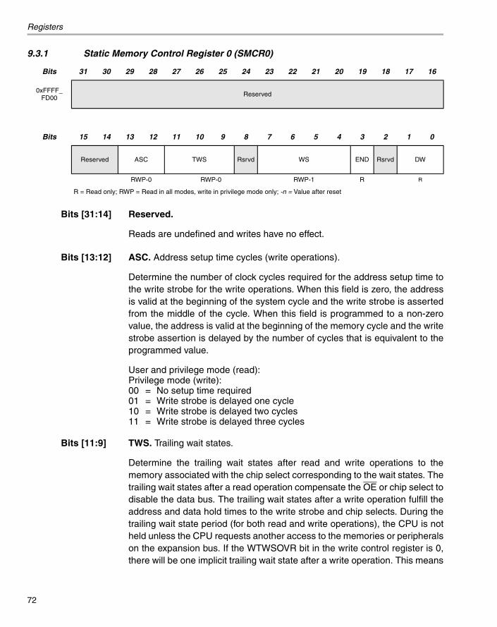
Registers
9.3.1 Static Memory Control Register 0 (SMCR0)
Bits [31:14] Reserved.
Reads are undefined and writes have no effect.
Bits [13:12] ASC. Address setup time cycles (write operations).
Determine the number of clock cycles required for the address setup time tothe write strobe for the write operations. When this field is zero, the addressis valid at the beginning of the system cycle and the write strobe is assertedfrom the middle of the cycle. When this field is programmed to a non-zerovalue, the address is valid at the beginning of the memory cycle and the writestrobe assertion is delayed by the number of cycles that is equivalent to theprogrammed value.
User and privilege mode (read):Privilege mode (write):00 = No setup time required01 = Write strobe is delayed one cycle10 = Write strobe is delayed two cycles11 = Write strobe is delayed three cycles
Bits [11:9] TWS. Trailing wait states.
Determine the trailing wait states after read and write operations to thememory associated with the chip select corresponding to the wait states. Thetrailing wait states after a read operation compensate the OE or chip select todisable the data bus. The trailing wait states after a write operation fulfill theaddress and data hold times to the write strobe and chip selects. During thetrailing wait state period (for both read and write operations), the CPU is notheld unless the CPU requests another access to the memories or peripheralson the expansion bus. If the WTWSOVR bit in the write control register is 0,there will be one implicit trailing wait state after a write operation. This means
Bits 31 30 29 28 27 26 25 24 23 22 21 20 19 18 17 16
0xFFFF_FD00 Reserved
Bits 15 14 13 12 11 10 9 8 7 6 5 4 3 2 1 0
Reserved ASC TWS Rsrvd WS END Rsrvd DW
RWP-0 RWP-0 RWP-1 R R
R = Read only; RWP = Read in all modes, write in privilege mode only; -n = Value after reset
72

Registers
that programming 0 or 1 in the TWS field in this register results in one trailingwait state after a write operation. If the WTWSOVR bit in the write controlregister is set to 1, the programmed value in the TWS field determines thenumber of trailing wait states for the write operation.
Bits [7:4] WS. Wait states (both read/write operations).
Each memory region can be programmed for up to 15 wait states. Each waitstate lasts one SYSCLK cycle period.
Table 19 lists the encoding for the wait-state bits.
† For devices with 470+ architecture, all expansion bus memory accesses are performed witha minimum of 1 wait state. Hence, for devices with 470+ architecture, if WS.3:0 = 0x00, thenthere is still 1 wait state. There are no other changes to this table for devices with 470+architecture.
Bit 3 END. Endian mode.
This is a read-only bit and represents the endian mode of the CPU and theboot memory.
User and privilege mode (read:)0 = CPU is in big endian mode.1 = CPU is in little endian mode.
Bit 2 Reserved.
The read/write values are indeterminate.
Bits [1:0] DW. Data width.
This field determines the data width of the memory region. Table 20 lists thebit encoding of this field.
User and privilege mode (read):Privilege mode (write)
Table 19. Wait State Definition for Memory Bank0
Encoding Number of Wait States
0000 0†
0001 1
: :
1111 15
System Module (SPNU189H) 73

Registers
Table 20. Data Widths for Data Memory Bank0
9.3.2 Registers SMCR1-SMCR9
The register diagrams on the following pages describe the bits for registersSMCR1 through SMCR9. For descriptions of each bit or group of bits, refer tothe above bit descriptions for register SMCR0 on page 72. Bits [2] and [3] forthe registers in the following sections function differently to those in SMCR0.The register tables are listed below. The descriptions for these bits are shownbelow.
9.3.3 Static Memory Control Registers (SMCRx)
Bit 3 END. Endian mode.
Determines the endianism of the memory region associated with thecorresponding chip select. When this bit is 0, the bytes are stored in bigendian mode. When this bit is 1, the bytes are stored in little endian mode.
User and privilege mode (read):Privilege mode (write):
0 = Bytes are stored in big endian mode for this memory select only.1 = Bytes are stored in little endian mode for this memory select only.
Encoding Mem Bank0 Data Width
00 8 bits
01 16 bits
10 32 bits
11 Reserved
Bits 31 30 29 28 27 26 25 24 23 22 21 20 19 18 17 16
0xFFFF_FDxx Reserved
Bits 15 14 13 12 11 10 9 8 7 6 5 4 3 2 1 0
Reserved ASC TWS Rsrvd WS END MLOC DW
RWP-0 RWP-0 RWP-1 RWP-0 RWP-0 RWP-0
R = Read Only; RWP = Read in all modes, write in privilege mode only; -n = Value after reset
74

Registers
Bit 2 MLOC. Memory location.
Determines the location of the memory; that is, whether memory is connectedto the internal expansion bus or an external expansion bus. This bit is used tosample the data from the associated data bus and to replace memory. Whenthis bit is set for external memory the internal chip select is deasserted, andwhen set for internal memory, the external chip select is deasserted.
0 = The memory is on the internal expansion bus.1 = The memory in on the external expansion bus.
9.4 Write Control Register (WCR0)
Bits [31:2] Reserved.
Reads are undefined and writes have no effect.
Bit 1 WTWSOVR. Write trailing wait state override.
When set to 1, there is no implicit trailing wait state after a write operation tothe memories; the number of wait states is determined by the TWS bit field inthe SMCRx register. When this bit is 0, there is always at least one trailingwait state on a write operation; if the TWS bit field in the SMCRx registers isnon-zero, the trailing wait states are determined by the TWS bit field.
User and privilege mode (read):Privilege mode (write):0 = At least one trailing wait state1 = TWS sets trailing wait states.
Bit 0 WBENABLE. Write buffer enable.
When this bit is set to 1, the memory controller latches the data and controlsignals in the first cycle for write operations to the memories and peripherals
Bits 31 30 29 28 27 26 25 24 23 22 21 20 19 18 17 16
0xFFFF_FD2C Reserved
Bits 15 14 13 12 11 10 9 8 7 6 5 4 3 2 1 0
ReservedWTWSOVR
WBEN-
ABLE
RWP-0 RWP-0
RWP = Read in all modes, write in privilege mode only; -n = Value after reset;
System Module (SPNU189H) 75

Registers
on the expansion bus and lets the CPU perform other operations. However,the CPU starts a wait state if there is another request before the memorycontroller finishes.
User and privilege mode (read):Privilege mode (write):0 = Write buffer disabled1 = Write buffer enabled
9.5 Peripheral Clock Register (PCR)
Bits [31:5] Reserved.
Read/write values are indeterminate.
Bits [4:1] CLKDIV. Peripheral clock divided ratio.
Determine the division ratio for ICLK with respect to SYSCLK. Table 21 onpage 77 describes the bit encoding for the ICLK/SYSCLK division ratios.
Bits 31 30 29 28 27 26 25 24 23 22 21 20 19 18 17 16
0xFFFF_FD30 Reserved
Bits 15 14 13 12 11 10 9 8 7 6 5 4 3 2 1 0
Reserved CLKDIVPEN-ABLE
RWP-1 RWP-0
RWP = Read in all modes, write in privilege mode only; -n = Value after reset;
76

Registers
Bit 0 PENABLE. Peripheral enable.
When this bit is set to 1, the peripheral reset is deasserted. After a reset theperipheral clock is SYSCLK /16.
The boot routine should set the CLKDIV field to the desired value before thePENABLE bit is set so that all the peripherals are in a reset state when theclock frequency is changed.
User and privilege mode (read):Privilege mode (write):0 = Peripheral reset is asserted. (default at reset)1 = Peripheral reset is deasserted.
Note: Peripherals not Accessible Until Enabled
User software must set the ICLK divider and then set PENABLE beforeperipherals can be accessed.
Table 21. Peripheral Clock Division Ratios
Bit Encoding ICLK
0000 ICLK = SYSCLK
0001 ICLK = SYSCLK/2
0010 ICLK = SYSCLK/3
0011 ICLK = SYSCLK/4
0100 ICLK = SYSCLK/5
0101 ICLK = SYSCLK/6
0110 ICLK = SYSCLK/7
0111 ICLK = SYSCLK/8
1000 ICLK = SYSCLK/9
1001 ICLK = SYSCLK/10
1010 ICLK = SYSCLK/11
1011 ICLK = SYSCLK/12
1100 ICLK = SYSCLK/13
1101 ICLK = SYSCLK/14
1110 ICLK = SYSCLK/15
1111ICLK = SYSCLK/16 (default at
reset)
System Module (SPNU189H) 77

Registers
9.6 Peripheral Location Register (PLR)
Bits [31:16] Reserved.
Reads are undefined and writes have no effect.
Bits [15:0] PLOC.15:0. Peripheral location bits.
The 16 bits of this register correspond to the 16 peripheral selects. Themapping of peripherals to peripheral selects is device specific. (See thedevice-specific data sheet for details of which peripheral select is tied towhich peripheral.)
Each bit corresponds to one peripheral select (bit 15 - PS[15]). The registerconfigures peripherals as internal or external.
User and privilege mode (read):Privilege mode (write):0 = The peripheral is internal.1 = The peripheral is external.
Bits 31 30 29 28 27 26 25 24 23 22 21 20 19 18 17 16
0xFFFF_FD34 Reserved
Bits 15 14 13 12 11 10 9 8 7 6 5 4 3 2 1 0
PLOC.15:0
RWP-0
RWP = Read in all modes, write in privilege mode only; -n = Value after reset;
78

Registers
9.7 Peripheral Protection Register (PPROT)
Bits [31:16] Reserved.
Reads are undefined and writes have no effect.
Bits [15:0] PPROT.15:0. Peripheral protection bits.
The 16 bits of this register correspond to the 16 peripheral selects. Themapping of peripherals to peripheral selects is device specific. (See thedevice-specific data sheet for details of which peripheral select is tied towhich peripheral.)
Each bit corresponds to one peripheral select (bit 15 - PS[15]). The registerconfigures peripherals so that they may be accessed in user and privilegemodes or in privilege mode only.
User and privilege mode (read):Privilege mode (write):0 = The peripheral is accessible in all modes.1 = The peripheral is accessible in privilege mode.
9.8 Memory Fine Base Address Registers
This section describes all the control registers that need to be programmedfor generating static memory selects and for providing memory protection.The structure of MFBAHR0 and MFBALR0 differs from the bit fields of theother MFBAHRx and MFBALRx registers.
There are six sets of fine base address control registers. MFBALR0 has aslightly different structure from the other MFBALRx registers; for this reason,MFBAHR0 and MFBALR0 are discussed first. The control registers from
Bits 31 30 29 28 27 26 25 24 23 22 21 20 19 18 17 16
0xFFFF_FD38 Reserved
Bits 15 14 13 12 11 10 9 8 7 6 5 4 3 2 1 0
PPROT.15:0
RWP-0
RWP = Read in all modes, write in privilege mode only; -n = Value after reset;
System Module (SPNU189H) 79

Registers
MFBAHR1 to MFBAHR5 and MFBALR1 to MFBALR5 have exactly the samestructure. The register addresses are listed in Table 22.
Table 22. Fine Base Control Register Addresses
Register Address
MFBAHR0 0xFFFF_FE00
MFBALR0 0xFFFF_FE04
MFBAHR1 0xFFFF_FE08
MFBALR1 0xFFFF_FE0C
MFBAHR2 0xFFFF_FE10
MFBALR2 0xFFFF_FE14
MFBAHR3 0xFFFF_FE18
MFBALR3 0xFFFF_FE1C
MFBAHR4 0xFFFF_FE20
MFBALR4 0xFFFF_FE24
MFBAHR5 0xFFFF_FE28
MFBALR5 0xFFFF_FE2C
80

Registers
9.8.1 Memory Fine Base Address High Register 0 (MFBAHR0)
9.8.2 Memory Fine Base Address Low Register 0 (MFBALR0)
Bits [31:10] Address.31:10. Base address.
The base address sets the 22 most significant bits of a memory address.When the top bits of an addressed location match the bits programmed intothe base address field, then this memory select is activated.
User and privilege mode (read):Privilege mode (write):
Address.31:10 = Contains the top 22 bits of the memory base address for thememory select.
Bit 9 Reserved. Reads are undefined and writes have no effect.
Bit 8 MS. Memory-map select.
Memory-map select enables the fine and coarse bus address registers asmemory selects and thereby activates the memory map.
Bits 31 30 29 28 27 26 25 24 23 22 21 20 19 18 17 16
0xFFFF_FE00 Reserved
Bits 15 14 13 12 11 10 9 8 7 6 5 4 3 2 1 0
Address.31:16
RWP-0
R = Read in all modes, WP = Write in privilege mode only; -n = Value after reset
Bits 31 30 29 28 27 26 25 24 23 22 21 20 19 18 17 16
0xFFFF_FE04 Reserved
Bits 15 14 13 12 11 10 9 8 7 6 5 4 3 2 1 0
Addres.15:10 MS Block Size 0 RONLY PRIV
RWP=0 RWP=0 RWP=0 RWP=0 RWP=0 RWP=0
R = Read in all modes, WP = write in privilege mode only; -n = Value after reset
System Module (SPNU189H) 81
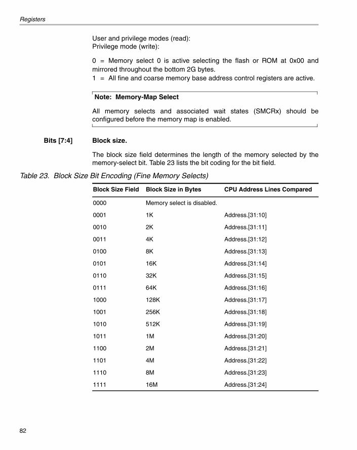
Registers
User and privilege modes (read):Privilege mode (write):
0 = Memory select 0 is active selecting the flash or ROM at 0x00 andmirrored throughout the bottom 2G bytes.1 = All fine and coarse memory base address control registers are active.
Note: Memory-Map Select
All memory selects and associated wait states (SMCRx) should beconfigured before the memory map is enabled.
Bits [7:4] Block size.
The block size field determines the length of the memory selected by thememory-select bit. Table 23 lists the bit coding for the bit field.
Table 23. Block Size Bit Encoding (Fine Memory Selects)
Block Size Field Block Size in Bytes CPU Address Lines Compared
0000 Memory select is disabled.
0001 1K Address.[31:10]
0010 2K Address.[31:11]
0011 4K Address.[31:12]
0100 8K Address.[31:13]
0101 16K Address.[31:14]
0110 32K Address.[31:15]
0111 64K Address.[31:16]
1000 128K Address.[31:17]
1001 256K Address.[31:18]
1010 512K Address.[31:19]
1011 1M Address.[31:20]
1100 2M Address.[31:21]
1101 4M Address.[31:22]
1110 8M Address.[31:23]
1111 16M Address.[31:24]
82
Registers
Bit 3 Reserved. Reserved for future use.
User must clear this bit to 0.
Bit 2 Reserved.
Reads are undefined and writes have no effect.
Bit 1 RONLY. Read-only protection.
The RONLY bit sets read-only protection for the memory region selected bythe memory select. An illegal access exception is generated when a write isattempted to the memory protected by read-only protection.
User and privilege modes (read):Privilege mode (write):0 = Read/write accesses to memory1 = Read accesses to memory only
Bit 0 PRIV. Privilege mode protection.
The PRIV bit sets privilege mode protection for the memory region selectedby the memory select. An illegal access exception is generated on anyaccess to memory protected by privilege mode protection if the CPU is in usermode.
User and privilege modes (read):Privilege mode (write):0 = User/privilege mode accesses to memory1 = Privilege mode accesses to memory only
System Module (SPNU189H) 83

Registers
9.8.3 Memory Fine Base Address High Register (MFBAHRx)
9.8.4 Memory Fine Base Address Low Register (MFBALRx)
Bit 9 AW. Auto-wait-on-write.
When this bit is set, any write operation on this memory select takes twosystem cycles.
0 = The write operation is not supplemented with an additional cycle.1 = The write operation takes an additional cycle.
The auto-wait-on-write bit AW (MFBALRx.8 and MCBALRx.8 [exceptMFBALR0]) holds the CPU for one cycle during a write operation. Theauto-wait-on-write is intended to support memories that latch address, select,and read/write signals on the same clock edge. This bit should not be usedfor expansion bus memory accesses.
Bits 31 30 29 28 27 26 25 24 23 22 21 20 19 18 17 16
0xFFFF_FExx Reserved
Bits 15 14 13 12 11 10 9 8 7 6 5 4 3 2 1 0
Address.31:16
RWP-0
R = Read in all modes, WP = Write in privilege mode only; -n = Value after reset
Bits 31 30 29 28 27 26 25 24 23 22 21 20 19 18 17 16
0xFFFF_FExx Reserved
Bits 15 14 13 12 11 10 9 8 7 6 5 4 3 2 1 0
Address.15:10 AW Rsrvd Block size Reserved RONLY PRIV
RWP-0 RWP-0 RWP-0 RWP-0 RWP-0
R = Read in all modes, WP = Write in privilege mode only; -n = Value after reset
84

Registers
9.9 Memory Coarse Select Control Registers
This section describes all the control registers which need to be programmedto generate chip-select signals and to provide protection for the memoryassociated with these coarse selects.
There are six sets of coarse base address control registers. The controlregisters from MCBAHR0 to MCBAHR5 and MCBALR0 to MCBALR5 haveexactly the same structure. The starting address for each register is listed inTable 24.
Table 24. Coarse Base Control Register Addresses
Register Address
MCBAHR0 0xFFFF_FE30
MCBALR0 0xFFFF_FE34
MCBAHR1 0xFFFF_FE38
MCBALR1 0xFFFF_FE3C
MCBAHR2 0xFFFF_FE40
MCBALR2 0xFFFF_FE44
MCBAHR3 0xFFFF_FE48
MCBALR3 0xFFFF_FE4C
MCBAHR4 0xFFFF_FE50
MCBALR4 0xFFFF_FE54
MCBAHR5 0xFFFF_FE58
MCBALR5 0xFFFF_FE5C
System Module (SPNU189H) 85

Registers
9.9.1 Memory Coarse Base Address High Register (MCBAHRx)
9.9.2 Memory Coarse Base Address Low Register (MCBALRx)
Bits [31:15] Address.31:15. Base address.
This base address sets the 17 most significant bits of a memory address.When the top bits of an addressed location match the bits programmed intothe base address field, then this memory select is activated.
User and privilege mode (read):Privilege mode (write):
Address.31:15 = Contains the top 17 bits of the memory base address for thememory select.
Bits [14:10] Reserved.
Reads are undefined and writes have no effect.
Bits 31 30 29 28 27 26 25 24 23 22 21 20 19 18 17 16
0xFFFF_FExx Reserved
Bits 15 14 13 12 11 10 9 8 7 6 5 4 3 2 1 0
Address.31:16
RWP-0
R = Read in all modes, WP = Write in privilege mode only; -n = Value after reset
Bits 31 30 29 28 27 26 25 24 23 22 21 20 19 18 17 16
0xFFFF_FExx Reserved]
Bits 15 14 13 12 11 10 9 8 7 6 5 4 3 2 1 0
Ad-dress.
15AW Block size 0 RONLY PRIV
RWP-0 RWP-0 RWP-0 RWP-0 RWP-0
R = Read in all modes, WP = Write in privilege mode only; -n = Value after reset
86

Registers
Bit 9 AW. Auto-wait-on-write.
When set, any write operation on this memory select takes an additionalsystem cycle.
0 = The write operation is completed in one cycle.1 = The write operation takes one additional cycle.
The auto-wait-on-write bit AW (MFBALRx.8 and MCBALRx.8 [exceptMFBALR0]) holds the CPU for one cycle during a write operation. Theauto-wait-on-write is intended to support memories that latch address, select,and read/write signals on the same clock edge. This bit should not be usedfor expansion bus memory accesses.
Bit 8 Reserved.
Reads are undefined and writes have no effect.
Bits [7:4] Block size.
The block size field determines the length of the memory selected by thememory select bit. Table 25 lists the bit coding for the bit field.
System Module (SPNU189H) 87

Registers
Bit 3 Reserved. Reserved for future use.
You must clear this bit to 0.
Bit 2 Reserved.
Reads are undefined and writes have no effect.
Bit 1 RONLY. Read-only protection.
The RONLY bit sets read-only protection for the memory region selected bythe memory select. An illegal access exception is generated when a write isattempted to the memory protected by read-only protection.
User and privilege modes (read):Privilege mode (write):0 = Read/write accesses to memory1 = Read accesses to memory only
Table 25. Block Size Bit Encoding (for Coarse Selects)
Block Size Field Block Size in Bytes CPU Address Bus Lines Compared
0000 Disables memory select
0001 32K Address.32:15
0010 64K Address.32:16
0011 128K Address.32:17
0100 256K Address.32:18
0101 512K Address.32:19
0110 1M Address.32:20
0111 2M Address.32:21
1000 4M Address.32:22
1001 8M Address.32:23
1010 16M Address.32:24
1011 32M Address.32:25
1100 64M Address.32:26
1101 128M Address.32:27
1110 256M Address.32:28
1111 512M Address.32:29
88

Registers
Bit 0 PRIV. Privilege mode protection.
The PRIV bit sets privilege mode protection for the memory region selectedby the memory select. An illegal access exception is generated on anyaccess to memory protected by privilege mode protection if the CPU is in usermode.
User and privilege modes (read):Privilege mode (write):0 = User/privilege mode accesses to memory1 = Privilege mode accesses to memory only
9.10 RTI Counter (RTICNTR)
The RTICNTR must be accessed with a word access. The RTI countercontains two separate counters. MOD counts down from the preload value(RTIPCTL) to 0. When MOD reaches 0, CNTR is incremented and PRELD isreloaded into MOD. MOD counts down and CNTR counts up.
Bits [31:11] CNTR.20:0. RTI Counter (counts up).
User and privilege mode (read):Tap and Compare interrupts are generated off this counter. Write access tothe RTICNTR will clear the CNTR (21 bit counter) and will cause a Tapinterrupt if the corresponding bit switches from a "1" to a "0". Therefore,disable the RTI prior to changing the RTICNTR value.See Section Table 6.,RTI Operating Modes, on page 30 for details of how to compute clock cycles.
Privilege mode (write):Any write resets the register.
Bits 31 30 29 28 27 26 25 24 23 22 21 20 19 18 17 16
0xFFFF_FF00 CNTR.20:5
RC-0
Bits 15 14 13 12 11 10 9 8 7 6 5 4 3 2 1 0
CNTR.4:0 MOD.10:0
RC-0 RC-0
R = Read in any mode, C = Clear in privileged mode only; -n = Value after reset
System Module (SPNU189H) 89

Registers
Bits [10:0] MOD.10:0. RTI module down counter.
User and privilege mode (read):Represents the current value of the modulo M counter within the RTI. SeeSection Table 6., RTI Operating Modes, on page 30 for details of how tocompute clock cycles.
Privilege mode (write):Any write resets the register and the preload value is loaded into MOD.
The values of both counters are read simultaneously as a 32-bit word.However, keep in mind that they are not a single 32-bit number but twonumbers of 21 bits and 11 bits, respectively. Furthermore, the modulo Mcounter is a down counter. Both counters do not stop while the device is innormal operating modes. The counters are cleared by a system reset. Thecounters are also cleared by a write to RTINCTR; a write resets CNTR andresets MOD to the preload value.
9.11 RTI Preload Control Register (RTIPCTL)
The RTI preload control register contains the preload value loaded into MOD(RTICNTR) and the tap select.
Bits [31:14] Reserved.
Reads are undefined and writes have no effect.
Bits [13:11] RTIM.2:0. Tap select.
User and privilege mode (read):Privilege mode (write):Configures tap select for the count-up counter (CNTR), as shown in Table 26.
Bits 31 30 29 28 27 26 25 24 23 22 21 20 19 18 17 16
0xFFFF_FF04 Reserved
Bits 15 14 13 12 11 10 9 8 7 6 5 4 3 2 1 0
Reserved RTIM.2:0 PRELD.10:0
RWP-0 RWP-0
R = Read in all modes, WP = write in privileged mode only; -n = Value after reset
90

Registers
Table 26. Tap Interrupts
Bits [10: 0] PRELD. Modulo M of preload value.
User and privilege mode (read):Privilege mode (write):
Holds the preload value M for the Modulo M counter. When the modulo Mcounter counts to 0, PRELD[10:0] is automatically loaded into the MODcounter. If the preloaded value is changed, it is recommended that RTICNTRbe written to so that it is cleared to ensure the module keeps the correct time.
RTIM.2:0Tap Bit
Tap Value
000 CNTR.20 RTICNTR.31 2097152
001 CNTR.17 RTICNTR.28 262144
010 CNTR.14 RTICNTR.25 32768
011 CNTR.11 RTICNTR.22 4096
100 CNTR.8 RTICNTR.19 512
101 CNTR.5 RTICNTR.16 64
110 CNTR.2 RTICNTR.13 8
111 Underflow Underflow 1
System Module (SPNU189H) 91

Registers
9.12 RTI Control Register (RTICNTL)
The RTI control register contains the tap enable and tap flag.
Bits [31:8] Reserved.
Reads are undefined and writes have no effect/
Bit 7 TAPFLAG. Tap interrupt flag bit.
The tap flag indicates that the transition edge (high-to-low) has occurred onthe selected tap bit of the CNTR. Once active, this bit remains set untilcleared.
User and privilege mode (read):0 = Transition has not occurred since last clear.1 = Transition has occurred since last clear.
Privilege mode (write):0 = Clears the bit1 = Has no effect
Bit 6 TAPENA. Tap interrupt enable bit.
Enables Tap interrupt.
User and privilege mode (read):Privilege mode (write):0 = Tap does not generate an interrupt request1 = Tap does generate an interrupt request
Bits [5:0] Reserved.
Reads are undefined and writes have no effect.
Bits 31 30 29 28 27 26 25 24 23 22 21 20 19 18 17 16
0xFFFF_FF08 Reserved
Bits 15 14 13 12 11 10 9 8 7 6 5 4 3 2 1 0
Reserved TAP FLAG
TAP ENA Reserved
RWP-0 RWP-0
R = read in all modes, W = Write in all modes; C = Clear; -n = Value after reset
92

Registers
9.13 Watchdog Key Register (WKEY)
Bits [31:0] WKEY.31:0. Key Sequence location.
User and privilege mode (read):Reads are indeterminate.
Privilege mode (write):A write of 0xE5 followed by 0xA3 in two separate write operations defines theKey Sequence and discharges the watchdog capacitor. Writing any othervalue causes a digital watchdog reset, as shown in Table 27.
Bits 31 30 29 28 27 26 25 24 23 22 21 20 19 18 17 16
0xFFFF_FF0C WKEY.31:16
WP-0
Bits 15 14 13 12 11 10 9 8 7 6 5 4 3 2 1 0
WKEY.15:0
WP-0
WP = Writable in privilege mode only; -n = Value after reset
Table 27. Example of a WKEY Sequence
StepValue Written to WKEY Result
1 0x0A3 No action
2 0x0A3 No action
3 0x0E5 WKEY is enabled for reset by the next 0x0A3.
4 0x0E5 WKEY is enabled for reset by the next 0x0A3.
5 0x0E5 WKEY is enabled for reset by the next 0x0A3.
6 0x0A3 Watchdog is reset.
7 0x0A3 No action
8 0x0E5 WKEY is enabled for reset by the next 0x0A3.
9 0x0A3 Watchdog is reset.
10 0x0E5 WKEY is enabled for reset by the next 0x0A3.
11 0x023 System reset; incorrect value written to WKEY
System Module (SPNU189H) 93

Registers
9.14 RTI Compare Register 1(RTICMP1)
Bits [31:21] Reserved.
Reads are undefined and writes have no effect.
Bits [20:0] COMPARE1. Compare value 1.
Value to be compared with CNTR[31:11]. When the value in CNTR[31:11]matches the value in COMPARE1[20:0], CF1 is set. The flag remains set untilcleared.
User and privilege (read):Privilege mode (write):
Compare value
9.15 RTI Compare Register 2(RTICMP2)
Bits [31:21] Reserved.
Reads are undefined and writes have no effect.
Bits 31 30 29 28 27 26 25 24 23 22 21 20 19 18 17 16
0xFFFF_FF10 Reserved COMPARE1.20:16
RWP-0
Bits 15 14 13 12 11 10 9 8 7 6 5 4 3 2 1 0
COMPARE1.15:0
RWP-0
R = Read in all modes, WP = Write in privilege mode only; -n = Value after reset
Bits 31 30 29 28 27 26 25 24 23 22 21 20 19 18 17 16
0xFFFF_FF14 Reserved COMPARE2.20:16
RWP-0
Bits 15 14 13 12 11 10 9 8 7 6 5 4 3 2 1 0
COMPARE2.15:0
RWP-0
R = Read in all modes, WP = Write in privilege mode only; -n = Value after reset
94

Registers
Bits [20:0] COMPARE2.20:0. Compare value 2.
Value to be compared with CNTR.31:11. Once the value in CNTR.31:11matches the value in COMPARE2.20:0, CF2 is set. The flag remains set untilcleared.
User and privilege (read):Privilege mode (write):
Compare value
9.16 Compare Interrupt Control Register (RTICINT)
The RTI compare interrupt control register contains flags and enables for thecompare interrupts.
Bits [31:8] Reserved.
Reads are undefined and writes have no effect.
Bit 7 CMP1 FLAG. Compare 1 Interrupt flag.
The CMP1 flag indicates that the CNTR value equals the value set inRTICMP1. Once active, this bit remains set until cleared.
User and privilege mode (read):0 = Equality compare has not occurred since last clear.1 = Equality compare has occurred since last clear.
Privilege mode (write):0 = Clears the bit.1 = Has no effect.
Bit 6 CMP2 FLAG. Compare 2 Interrupt flag.
Bits 31 30 29 28 27 26 25 24 23 22 21 20 19 18 17 16
0xFFFF_FF18 Reserved
Bits 15 14 13 12 11 10 9 8 7 6 5 4 3 2 1 0
Reserved CMP1FLAG
CMP2 FLAG
CMP1 ENA
CMP2 ENA Reserved
RWP-0 RWP-0 RWP-0 RWP-0
R = Read in all modes, WP = Write in privilege mode only; -n = Value after reset
System Module (SPNU189H) 95

Registers
The CMP2 flag indicates that the CNTR value equals the value set inRTICMP2. Once active, this bit remains set until cleared.
User and privilege mode (read):0 = Equality compare has not occurred since last clear.1 = Equality compare has occurred since last clear.
Privilege mode (write):0 = Clears the bit.1 = Has no effect.
Bit 5 CMP1 ENA. Compare 1 enable.
Enables the compare 1 register.
User and privilege mode (read):Privilege mode (write):0 = CMP1 does not generate an interrupt request.1 = CMP1 generates an interrupt request.
Bit 4 CMP2 ENA. Compare 2 Interrupt enable.
Enables the compare 2 interrupt register.
User and privilege mode (read):Privilege mode (write):0 = CMP1 does not generate an interrupt request.1 = CMP1 generates an interrupt request.
Bits [3:0] Reserved.
Reads are undefined and writes have no effect.
96

Registers
9.17 RTI Count Enable Register (RTICNTEN)
Bits [31:2] Reserved.
Reads are undefined and writes have no effect.
Bits [1:0] CNTEN.1:0.
Based on the CPU operating mode, allows the MOD and CNTR counters(RTICNTR) within the RTI to count or not. Table 28 lists the CPU modes inwhich count activity is allowed to occur.
User and privilege mode (read):Privilege mode (write):
9.18 CIM Offset Vector Registers
The CIM offset register provides the user with the numerical index value thatrepresents the pending interrupt with the highest precedence. (IRQIVECholds the index to the highest priority IRQ interrupt; FIQIVEC holds the indexto the highest priority FIQ interrupt; and CIMIVEC holds the index to thehighest priority interrupt based on the state of the CPU). The index can be
Bits 31 30 29 28 27 26 25 24 23 22 21 20 19 18 17 16
0xFFFF_FF1C Reserved
Bits 15 14 13 12 11 10 9 8 7 6 5 4 3 2 1 0
Reserved CNTEN.1:0
RWP-0
R = Read in all modes, WP = Write in privilege mode only; -n = Value after reset
Table 28. Real-Time Interrupt Counter Enable Modes
CNTEN1 CNTEN0 Count
0 0 User/privilege
0 1 Privilege only
1 0 User only
1 1 No count
System Module (SPNU189H) 97

Registers
used to locate the interrupt routine in a dispatch table, as shown in Table 29.Reading any of these registers clears the interrupt flag as well as the offset.
The CIM offset registers are read only. They are updated continuously by theCIM. Once the interrupt is serviced, the offset vectors show the index for thenext highest pending interrupt or if no interrupt is pending, 0x00.
9.18.1 IRQ Index Offset Vector Register (IRQIVEC)
The IRQ offset register provides the user with the numerical index value thatrepresents the highest priority, pending IRQ interrupt.
Bits [31:8] Reserved.
Reads are undefined and writes have no effect.
Bits [7:0] IRQIVEC.7:0. Index vector.
User and privilege mode (read):The least significant bits represent the index of the IRQ pending interrupt withthe highest precedence, as shown in Table 29. When no interrupts arepending, the least significant byte of IRQIVEC is 0x00. A read clears theoffset and the pending interrupt flag.
Table 29. Interrupt Dispatch Table
IVEC Index Pending Interrupt
0x00 No interrupt
0x01 Channel 0
: :
0x20 Channel 31
Bits 31 30 29 28 27 26 25 24 23 22 21 20 19 18 17 16
0xFFFF_FF20 Reserved
Bits 15 14 13 12 11 10 9 8 7 6 5 4 3 2 1 0
Reserved IRQIVEC.7:0
R-0
R = Read only; -n = Value after reset
98

Registers
User and privilege mode (write):Writes have no effect.
9.18.2 FIQ Index Offset Vector Registers (FIQIVEC)
The FIQIVEC register provides the user with a numerical index value thatrepresents the highest priority pending FIQ interrupt.
Bits [31:8] Reserved.
Reads are undefined and writes have no effect.
Bits [7:0] FIQIVEC.7:0. Index vector.
User and privilege mode (read):The least significant bits represent the index of the FIQ pending interrupt withthe highest precedence, as shown in Table 29. When no interrupts arepending, the least significant byte of FIQIVEC is 0x00. A read clears the offsetand the pending interrupt flag.
User and privilege mode (write):Writes have no effect.
Bits 31 30 29 28 27 26 25 24 23 22 21 20 19 18 17 16
0xFFFF_FF24 Reserved
Bits 15 14 13 12 11 10 9 8 7 6 5 4 3 2 1 0
Reserved FIQIVEC.7:0
R-0
R = Read only; -n = Value after reset
System Module (SPNU189H) 99

Registers
9.18.3 CIM Index Offset Vector Register (CIMIVEC)
The CIMIVEC offset register provides the user with the numerical index valuethat represents the highest priority pending interrupt. The CIMIVEC returnsthe highest priority IRQ interrupt when the CPU is in IRQ mode, and theCIMIVEC returns the highest priority FIQ interrupt when the CPU is in FIQmode.
Bits [31:8] Reserved.
Reads are undefined and writes have no effect.
Bits [7:0] CIMIVEC.7:0. Index vector.
User and privilege mode (read):The least significant bits represent the index of the pending interrupt with thehighest precedence, as shown in Table 29. When no interrupts are pending,the least significant byte of CIMIVEC is 0x00. A read clears the offset and thepending interrupt flag.
User and privilege mode (write):Writes have no effect.
Bits 31 30 29 28 27 26 25 24 23 22 21 20 19 18 17 16
0xFFFF_FF28 Reserved
Bits 15 14 13 12 11 10 9 8 7 6 5 4 3 2 1 0
Reserved CIMIVEC.7:0
R-0
R = Read only; -n = Value after reset
100

Registers
9.19 FIQ/IRQ Program Control Register (FIRQPR)
A 32-bit FIQ/IRQ program control register (FIRQPR) determines whether agiven interrupt request will be FIQ or IRQ type.
Bits [31:0] FIRQPR.31:0. FIQ/IRQ program control bits.
These bits determine whether an interrupt request from a peripheral is of typeFIQ or IRQ. Each bit corresponds to one request channel.
User and privilege mode (read):Privilege mode (write):0 = Interrupt request is of IRQ type.1 = Interrupt request is of FIQ type.
9.20 Pending Interrupt Read Location (INTREQ)
The pending interrupt register gives the pending interrupt requests. Theregister is updated every SYSCLK cycle.
Bits [31:0] INTREQ.31:0. Pending interrupt bits.
Determines whether an interrupt request is pending.
Bits 31 30 29 28 27 26 25 24 23 22 21 20 19 18 17 16
0xFFFF_FF2C FIRQPR.31:16
RWP-0
Bits 15 14 13 12 11 10 9 8 7 6 5 4 3 2 1 0
FIRQPR.15:0
RWP-0
R = Read in all modes, WP = Writable in privilege mode only; -n = Value after reset
Bits 31 30 29 28 27 26 25 24 23 22 21 20 19 18 17 16
0xFFFF_FF30 INTREQ.31:16
RWP-0
Bits 15 14 13 12 11 10 9 8 7 6 5 4 3 2 1 0
INTREQ.15:0
RWP-0
R = Read in all modes, WP = Writable in privilege mode only; -n = Value after reset
System Module (SPNU189H) 101

Registers
User and privilege mode (read):Privilege mode (write):0 = No interrupt event has occurred.1 = Interrupt is pending.
9.21 Interrupt Mask Register (REQMASK)
The interrupt register mask selectively disables individual request channels.
Bits [31:0] REQMASK.31:0. Request mask bits.
This vector determines whether the interrupt request channel is enabled.
User and privilege mode (read):Privilege mode (write):0 = Interrupt request channel is disabled.1 = Interrupt request channel is enabled.
Bits 31 30 29 28 27 26 25 24 23 22 21 20 19 18 17 16
0xFFFF_FF34 REQMASK.31:16
RWP-0
Bits 15 14 13 12 11 10 9 8 7 6 5 4 3 2 1 0
REQMASK.15:0
RWP-0
R = Read in all modes, WP = Writable in privilege mode only; -n = Value after reset
102

Registers
9.22 CPU Data Bus Parallel Signature Analysis Register (CPUPSA)
The CPU data bus parallel signature analysis contains the original sendvalue. During and after the PSA runs, CPUPSA contains the currentsignature.
Bits [31:0] CPUPSA.31:0. Contains the current signature result.
To initialize the PSA, a seed value must first be written. Based on the currentdata on the CPU bus, a signature value is generated. This value can then becompared to expected signature values (usually generated by an externaltool).
9.23 PSA Enable (PSAENABLE)
The least significant bit (PSADIS) enables the PSA.
Bits [31:1] Reserved.
Reads are undefined and writes have no effect.
Bits 31 30 29 28 27 26 25 24 23 22 21 20 19 18 17 16
0xFFFF_FF40 CPUPSA.31:16
RW-0
Bits 15 14 13 12 11 10 9 8 7 6 5 4 3 2 1 0
CPUPSA.15:0
RW-0
RW = Read/write; -n = Value after reset
Bits 31 30 29 28 27 26 25 24 23 22 21 20 19 18 17 16
0xFFFF_FF50 Reserved
Bits 15 14 13 12 11 10 9 8 7 6 5 4 3 2 1 0
Reserved PSA-DIS
RW-0
RW = Read/write; -n = Value after reset
System Module (SPNU189H) 103

Registers
Bit 0 PSADIS.
Enables the corresponding PSA module
0 = PSA enabled1 = PSA disabled
9.24 New Global Control Register (GCR_N)
Bits[32:14] Reserved
Reads are undefined and writes have no effect.
Bits [15:0] PLL Specific.
See the specific PLL user guide document for additional details on thePLL-specific bits.
Bits 31 30 29 28 27 26 25 24 23 22 21 20 19 18 17 16
0xFFFF_FFCC Reserved
Bits 15 14 13 12 11 10 9 8 7 6 5 4 3 2 1 0
PLL Specific
RW = Read/write; -n = Value after reset
104

Registers
9.25 Clock Control Register (CLKCNTL)
The clock control register configures the CLKOUT pin and a bit that controlsthe module low power mode.
CLKCNTL is accessible in user and privilege mode and supports byte, half-word, and word accesses. Any access to this register takes two SYSCLKcycles.
Bits [31:8] Reserved.
Reads are undefined and writes have no effect.
Bit 7 PPWNOVR. Peripheral power down enable.
The PPWNOVR enables the power down of clocks to the control registers ofthe module. The PPWNOVR bit works with the power-down bit in a givenmodule. Typically, when the module is powered down via the module level bit,the clocks to the module’s logic stop; when the module is powered down andPPWNOVR is set, the clocks to both the logic and the control registers arestopped. To manually wake a module, the PPWNOVR must be cleared andthe power-down bit at the module must be serviced.
User and privilege mode (read/write):0 = All peripheral control registers are clocked.1 = Control registers of the peripherals that are powered down are not
clocked.
Bits 31 30 29 28 27 26 25 24 23 22 21 20 19 18 17 16
0xFFFF_FFD0 Reserved
Bits 15 14 13 12 11 10 9 8 7 6 5 4 3 2 1 0
Reserved PPWNOVR CLKSR CLK
DIRCLK
DOUTCLKDIN LPM
RW-0 RW-0 RW-0 RW-0 R-0 RW-0
R = Read in all modes, W = Write in all modes.; -n = Value after reset
System Module (SPNU189H) 105

Registers
Bits [6:5] CLKSR. Clock source bits.
Controls the source/function of the CLKOUT pin. (See Table 30.) The possibleconfigurations for the CLKOUT pin are as follows:
User and privilege mode (read/write):00 = Configured as a digital input/output pin01 = Driven by the interface clock (ICLK)10 = Driven by the CPU clock (MCLK)11 = Driven by the system clock (SYSCLK)
Bit 4 CLKDIR. CLKOUT pin direction.
If the CLKOUT pin is selected as a digital I/O pin, this bit determines whetherthe CLKOUT pin is an input or output pin; otherwise this bit has no effect. (SeeTable 30.)
User and privilege mode (read/write):0 = CLKOUT pin is configured as an input.1 = CLKOUT pin is configured as an output.
Bit 3 CLKDOUT. CLKOUT output pin data.
If the CLKOUT pin is configured as a digital I/O and as an output pin(CLKSR=0x00 and CKDIR=1), This bit will place either a logic value 0 or 1 tothe pin; otherwise this bit has no effect. (See Table 30.)
User and privilege mode (read/write):0 = Logic low (output voltage on CLKOUT is VOL or lower)1 = Logic high (output voltage on CLKOUT is VOH or higher)
Bit 2 CLKDIN. CLKOUT input pin data.
If the CLKOUT pin is configured as a digital I/O and as an input pin (CLKSR = 0x00 and CKDIR = 0), this bit represents the logic value on the pin;otherwise, this bit has no effect. (See Table 30.)
User and privilege mode (read):0 = Logic low (input voltage on CLKOUT is VIL or lower)1 = Logic high (input voltage on CLKOUT is VIH or higher)
User and privilege mode (write):Writes have no effect.
106
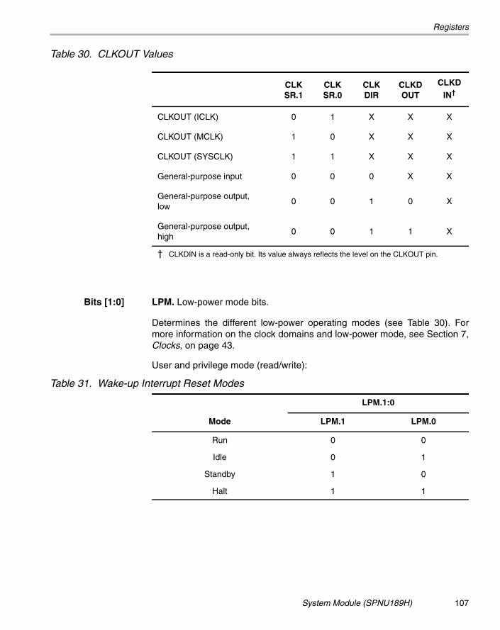
Registers
Table 30. CLKOUT Values
Bits [1:0] LPM. Low-power mode bits.
Determines the different low-power operating modes (see Table 30). Formore information on the clock domains and low-power mode, see Section 7,Clocks, on page 43.
User and privilege mode (read/write):
CLKSR.1
CLKSR.0
CLKDIR
CLKDOUT
CLKDIN†
CLKOUT (ICLK) 0 1 X X X
CLKOUT (MCLK) 1 0 X X X
CLKOUT (SYSCLK) 1 1 X X X
General-purpose input 0 0 0 X X
General-purpose output, low
0 0 1 0 X
General-purpose output, high
0 0 1 1 X
† CLKDIN is a read-only bit. Its value always reflects the level on the CLKOUT pin.
Table 31. Wake-up Interrupt Reset Modes
Mode
LPM.1:0
LPM.1 LPM.0
Run 0 0
Idle 0 1
Standby 1 0
Halt 1 1
System Module (SPNU189H) 107

Registers
9.26 Global Control Register (GLBCTRL)
The global control register controls the PLL and one bit that configures theflash. See the specific PLL user guide document for additional details on thePLL specific bits.
Further, any write to this register asserts three wait states.
Bits [31:16] Reserved.
Reads are undefined and writes have no effect.
Bits [15:5] PLL Specific.
See the specific PLL user guide document for additional details on thePLL-specific bits.
Bit 4 FLCONFIG. Flash configuration mode bit.
Controls write access to the flash wrapper’s control registers. See the flashwrapper user specification for details on the flash wrapper’s control registers.
User and privilege mode (read):Privilege mode (write):0 = No read or write access allowed; read or write access to the flash
control registers generates an illegal address exception.1 = Allows read or write access to flash wrapper’s control register
Bit [3:0] PLL Specific.
See the specific PLL user guide document for additional details on thePLL-specific bits
Note: Device with Enhanced RTI
Bits 31 30 29 28 27 26 25 24 23 22 21 20 19 18 17 16
0xFFFF_FFDC Reserved
Bits 15 14 13 12 11 10 9 8 7 6 5 4 3 2 1 0
PLLSpecific
FLCON-FIG
PLL Specific
RWP-0
R = Read in all modes, WP = write in privilege mode only; -n = Value after reset
108

Registers
On a device with an enhanced RTI, the RTI may be clocked at OSCIN orSYSCLK frequencies. Additionally, the PLL may be disabled during stand-by.(See the device-specific data sheet regarding enhanced RTI.)
Bits 15 PLL Specific.
See the specific PLL user guide document for additional details on thePLL-specific bits.
Bits 14 RTI OSC EN. RTI Oscillator Enable.
When this bit is set, the RTI will run using the clock generated by theoscillator. This bit is implemented only on the Enhanced RTI Module. (See thedevice-specific data sheet to see if this feature has been implemented).
User and privilege mode (read/write):
0 = This is the default state for the bit. The RTI is clocked directly from theclock control module at system clock speed.
1 = The RTI is clocked directly from the oscillator.
Bits 13 PLL STBY DIS. PLL Standby Disable.
When this bit is set, the PLL will be disabled upon entering standby mode.This bit is only effective in standby mode.
User and privilege mode (read/write):
0 = PLL is enabled1 = PLL is disabled
Bits 31 30 29 28 27 26 25 24 23 22 21 20 19 18 17 16
0xFFFF_FFDC Reserved
Bits 15 14 13 12 11 10 9 8 7 6 5 4 3 2 1 0
PLLSpecific
RTIOSCEN
PLLSTBYDIS
PLL SpecificFL
CON-FIG
PLL Specific
RW-0 RW-0 RWP-0
R = Read in all modes, WP = write in privilege mode only; -n = Value after reset
System Module (SPNU189H) 109

Registers
9.27 System Exception Control Register (SYSECR)
The system exception control register contains bits that allow the user togenerate a software reset; the OVR bits disable some reset/abort conditionswhen TRST is high.
Bits [31:16] Reserved.
Reads are undefined and writes have no effect.
Bits [15:14] RESET. Software reset bits.
Setting RESET or clearing RESET causes a software reset. There are threepossible reset cases:
User and privilege mode (read):Always reads 01
Bits 31 30 29 28 27 26 25 24 23 22 21 20 19 18 17 16
0xFFFF_FFE0 Reserved
Bits 15 14 13 12 11 10 9 8 7 6 5 4 3 2 1 0
RESET RESET Reserved PACCOVR
ACCOVR
ILLOVR
RWP-0 RWP-1 RWP-0 RWP-0 RWP-0
R = Read in all modes, WP = write in privilege mode only; -n = Value after reset
110
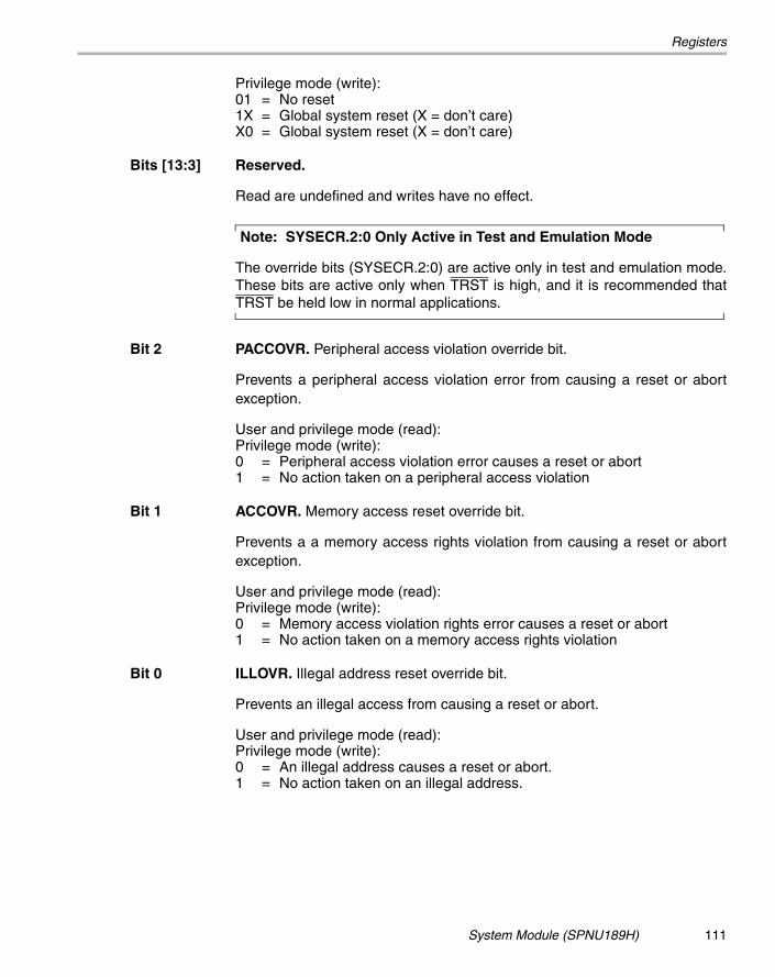
Registers
Privilege mode (write):01 = No reset1X = Global system reset (X = don’t care)X0 = Global system reset (X = don’t care)
Bits [13:3] Reserved.
Read are undefined and writes have no effect.
Note: SYSECR.2:0 Only Active in Test and Emulation Mode
The override bits (SYSECR.2:0) are active only in test and emulation mode.These bits are active only when TRST is high, and it is recommended thatTRST be held low in normal applications.
Bit 2 PACCOVR. Peripheral access violation override bit.
Prevents a peripheral access violation error from causing a reset or abortexception.
User and privilege mode (read):Privilege mode (write):0 = Peripheral access violation error causes a reset or abort1 = No action taken on a peripheral access violation
Bit 1 ACCOVR. Memory access reset override bit.
Prevents a a memory access rights violation from causing a reset or abortexception.
User and privilege mode (read):Privilege mode (write):0 = Memory access violation rights error causes a reset or abort1 = No action taken on a memory access rights violation
Bit 0 ILLOVR. Illegal address reset override bit.
Prevents an illegal access from causing a reset or abort.
User and privilege mode (read):Privilege mode (write):0 = An illegal address causes a reset or abort.1 = No action taken on an illegal address.
System Module (SPNU189H) 111

Registers
9.28 System Reset Exception Status Register (SYSESR)
The system reset exception status register contains flags for different reset/abort sources. On power-up, all bits are cleared to 0. When a reset conditionis recognized, the appropriate bit in SYSESR is set and the value of the bit ismaintained through the reset (as long as VCC remains within specifications).See Section 6, Resets, on page 41 for further information about the causesof resets.
When a new reset condition occurs, the current contents of this register arenot cleared. The contents of this register are cleared on a power-on reset orby software.
Note: The PORRST Bit
The PORRST bit is always set when the device is powered up. The bit iscleared to 0 on power up, but is active whenever the PORRST pin is low. ThePORRST pin is low coming out of power up, so the bit is always set to 1.
Bits [31:16] Reserved.
Reads are undefined and writes have no effect.
Bit 15 PORRST. Power-up reset flag.
Set when Power-On Reset is asserted. Reset is asserted as long as Power-On Reset is active. Whenever a device is powered, this bit is set.
User and privilege modes (read):0 = Power-up reset has not occurred since the last clear.1 = Power-up reset has occurred since the last clear.
User and privilege modes (write):0 = Clears the corresponding bit to 01 = Has no effect
Bits 31 30 29 28 27 26 25 24 23 22 21 20 19 18 17 16
0xFFFF_FFE4 Reserved
Bits 15 14 13 12 11 10 9 8 7 6 5 4 3 2 1 0
PORRST
CLKRST
WDRST
ILLMODE
ILLADR
ILLACC
PILLACC
ILLMAP
SWRST Reserved
RC-X RC-X RC-X RC-X RC-X RC-X RC-X RC-X RC-X
R = Read in all modes, Clear = Clear in all modes by writing a 0; -X = Value unchanged after reset
112

Registers
Bit 14 CLKRST. Clock fail flag.
Indicates that a clock fault condition has occurred. When power-up resetoccurs, the CLKRST is reset to 0. Value remains unchanged during otherresets.
User and privilege modes (read):0 = A clock failure has not occurred since the last clear.1 = A clock failure has occurred since the last clear.
User and privilege modes (write):0 = Clears the corresponding bit to 0.1 = Has no effect.
Bit 13 WDRST. Watchdog reset flag.
Set when the last reset is caused by the watchdog.
User and privilege modes (read):0 = A watchdog reset has not occurred since the last clear.1 = A watchdog reset has occurred since the last clear.
User and privilege modes (write):0 = Clears the corresponding bit to 0.1 = Has no effect.
Bit 12 ILLMODE. Illegal mode flag.
Set when the mode bits in the program status register are set to an illegalvalue.
User and privilege modes (read):0 = An illegal mode has not occurred since the last clear.1 = An illegal mode has occurred since the last clear.
User and privilege modes (write):0 = Clears the corresponding bit to 0.1 = Has no effect.
Bit 11 ILLADR. Illegal address access flag.
Set when an access to an unimplemented location in the memory map isdetected in non-user mode.
User and privilege modes (read):0 = An illegal address has not occurred since the last clear.1 = An illegal address has occurred since the last clear.
User and privilege modes (write):0 = Clears the corresponding bit to 01 = Has no effect
System Module (SPNU189H) 113

Registers
Bit 10 ILLACC. Illegal memory access flag.
Set when an access to a protected location without permission rights isdetected in non-user mode.
User and privilege modes (read):0 = An illegal memory access has not occurred since the last clear.1 = An illegal memory access has occurred since the last clear.
User and privilege modes (write):0 = Clears the corresponding bit to 01 = Has no effect
Bit 9 PILLACC. Peripheral illegal access flag.
Set when a peripheral access violation is detected in user mode.
User and privilege modes (read):0 = An illegal peripheral access has not occurred since the last clear.1 = An illegal peripheral access has occurred since the last clear.
User and privilege modes (write):0 = Clears the corresponding bit to 01 = Has no effect
Bit 8 ILLMAP. Illegal address map flag.
Set when the base addresses of one or more memories overlap. Resetoccurs when the overlapped region is accessed.
User and privilege modes (read):0 = An illegal address mapping has not occurred since the last clear.1 = An illegal address mapping has occurred since the last clear.
User and privilege modes (write):0 = Clears the corresponding bit to 01 = Has no effect
Bit 7 SWRST. Software reset flag.
Set when the last reset is caused by software writing to the RESET bits.
User and privilege modes (read):0 = A software reset has not occurred since the last clear.1 = A software reset has occurred since the last clear.
User and privilege modes (write):0 = Clears the corresponding bit to 01 = Has no effect
114

Registers
Bits [6:0] Reserved.
Reads are undefined and writes have no effect.
9.29 Abort Exception Status Register (ABRTESR)
The abort exception status register shows the abort cause. For moreinformation on aborts, see Section 6, Resets, on page 41 and Section 3.4,Memory Resets, on page 21.
Bits [31:16] Reserved.
Reads are undefined and writes have no effect.
Bit 15 ADRABT. Illegal address abort.
An illegal address access was detected in user mode. An abort wasgenerated due to an illegal address access from either the MPU or system.
User and privilege mode (read):0 = No illegal address1 = Abort caused by an illegal address
User and privilege mode (write):0 = Clears bit to 01 = Has no effect
Bit 14 MEMABT. Memory access abort.
Indicates an illegal memory access was detected in user mode. An abort wasgenerated due to the illegal memory access from either the MPU or system.
User and privilege mode (read):0 = No illegal memory access1 = Abort caused by an illegal memory access
Bits 31 30 29 28 27 26 25 24 23 22 21 20 19 18 17 16
0xFFFF_FFE8 Reserved
Bits 15 14 13 12 11 10 9 8 7 6 5 4 3 2 1 0
ADRABT
MEMABT
PACCVIO Reserved
RC-0 RC-0 RC-0
RC = Read in all modes, C = Clear in all modes by writing a 0; -n = Value after reset;
System Module (SPNU189H) 115

Registers
User and privilege mode (write):0 = Clears bit to 01 = Has no effect
Bit 13 PACCVIO. Peripheral access violation error.
Indicates a peripheral access violation error was detected during a peripheralregister access in user mode. An abort was generated due to a peripheralaccess violation.
User and privilege mode (read):0 = No peripheral access violation1 = Abort caused by an peripheral access violation
User and privilege mode (write):0 = Clears bit to 01 = Has no effect
Bits [12:0] Reserved.
Reads are undefined and writes have no effect.
9.30 Global Status Register (GLBSTAT)
The global status register specifies the module that triggered the illegaladdress, illegal access, abort, or reset.
When a new reset condition occurs, the current contents of this register arenot cleared. The contents of this register are cleared on a power-on reset orby software.
Bits [31:8] Reserved.
Bits 31 30 29 28 27 26 25 24 23 22 21 20 19 18 17 16
0xFFFF_FFEC Reserved
Bits 15 14 13 12 11 10 9 8 7 6 5 4 3 2 1 0
Reserved SYSADDR
SYSACC
MPUADDR
MPUACC Reserved OSC
FAILPLLSLIP
RC-X RC-X RC-X RC-X RC-X RC-X
R = Read in all modes, C = Clear in all modes by writing a 0; -X = Value unchanged after reset
116

Registers
Reads are undefined and writes have no effect. To maintain futurecompatibility of software, initialize these bits to 0.
Bit 7 SYSADDR. System illegal address flag.
Set when the system detects an illegal address.
User and privilege mode (read):0 = No system illegal address1 = Abort or reset caused by a system illegal address
User and privilege mode (write):0 = Clears bit to 01 = Has no effect
Bit 6 SYSACC. System illegal access flag.
Set when the system detects an illegal access.
User and privilege mode (read):0 = No system illegal access1 = Abort or reset caused by a system illegal access
User and privilege mode (write):0 = Clears bit to 01 = Has no effect
Bit 5 MPUADDR. MPU illegal address flag.
Set when the memory protection unit (MPU) detects an illegal address.
User and privilege mode (read):0 = No MPU illegal address1 = Abort or reset caused by a MPU illegal address
User and privilege mode (write):0 = Clears bit to 01 = Has no effect
Bit 4 MPUACC. MPU illegal access flag.
Set when the memory protection unit (MPU) detects an illegal access. (TheMPUACC flag is set along with the MPUADDR flag when an MPU illegaladdress is detected. See Section 3.4.1, Illegal Address, on page 22.)
User and privilege mode (read):0 = No MPU illegal access1 = Abort or reset caused by a MPU illegal access
System Module (SPNU189H) 117

Registers
User and privilege mode (write):0 = Clears bit to 01 = Has no effect
Bits [3:2] Reserved.
Reads are undefined and writes have no effect. To maintain futurecompatibility of software, initialize these bits to 0.
Bit 1 OSCFAIL. Oscillator Fail Flag Bit.
When set, this bit indicates that the external reference (oscillator or crystal) isoperating at a frequency too slow to be functional when compared to aninternal reference oscillator. For more information, see Section 6, Resets, onpage 41.
User and privilege mode (read):0 = No oscillator failure1 = Abort caused by an oscillator failure
User and privilege mode (write):0 = Clears bit to 01 = Has no effect
Bits 0 PLLSLIP. PLL Slip Flag Bit.
When set, this bit indicates that a discrepancy between the reference andVCO oscillator phases has been detected. This bit can be read and filtered inuser software to determine if the slip is caused by noise or is deemed to be atrue failure. For more information, see Section 6, Resets, on page 41.
User and privilege mode (read):0 = No PLL slip1 = Abort caused by a PLL slip
User and privilege mode (write):0 = Clears bit to 01 = Has no effect
118

Registers
9.31 Device Identification Register (DEV)
The register contains device-specific information that is hard coded duringdevice manufacture.
Bits [31:16] Reserved.
Reads are undefined and writes have no effect. To maintain futurecompatibility of software, initialize these bits to 0.
Bits [15:0] DEV.15:0. Device identification code.
This is a read-only register. See the device-specific data sheet for details onthe device identification code.
Bits 31 30 29 28 27 26 25 24 23 22 21 20 19 18 17 16
0xFFFF_FFF0 Reserved
Bits 15 14 13 12 11 10 9 8 7 6 5 4 3 2 1 0
DEV.15:0
R-K
R = Read only; -K = Constant value
System Module (SPNU189H) 119

Registers
9.32 System Software Interrupt Flag Register (SSIF)
The system software interrupt flag is set when a software interrupt istriggered. The flag allows the user to poll for a software interrupt.
Bits [31:1] Reserved.
Reads are undefined and writes have no effect.
Bit 0 SSIF. System software interrupt flag.
Set when a correct SSKEY is written to the SSIR register. Cleared only bysoftware. Possible values are as follows:
User and privilege mode (read):0 = No IRQ/FIQ interrupt request has been generated since the last clear.1 = An IRQ/FIQ interrupt request has been generated since the last clear.
User and privilege mode (write):0 = Clears the bit1 = Has no effect
Bits 31 30 29 28 27 26 25 24 23 22 21 20 19 18 17 16
0xFFFF_FFF8 Reserved
Bits 15 14 13 12 11 10 9 8 7 6 5 4 3 2 1 0
Reserved SSIFLAG
RC-0
R = Read, C = Clear; -n = Value after reset
120

Registers
9.33 System Software Interrupt Request Register (SSIR)
The system software interrupt request register contains a key sequence thattriggers a software interrupt request to the CIM. Also, the register contains an8-bit data field.
Bits [31:16] Reserved.
Reads are undefined and writes have no effect.
Bits [15:8] SSKEY.7:0. System software interrupt request key.
Write-only data bits executable in user and privilege modes. A 0x75 written tothese bits initiates IRQ/FIQ interrupts. Data in this field is always read as zero(0).
Bits [7:0] SSDATA.7:0. System software interrupt data.
User and privilege mode (read/write):SSDATA provides an 8-bit field that can be used for passing messages intothe system software interrupt.
Bits 31 30 29 28 27 26 25 24 23 22 21 20 19 18 17 16
0xFFFF_FFFC Reserved
Bits 15 14 13 12 11 10 9 8 7 6 5 4 3 2 1 0
SSKEY.7:0] SSDATA.7:0
W-0 RW-0
R = Reads, W = Writes; -n = Value after reset
System Module (SPNU189H) 121

Registers
122


