Embed Size (px)
Citation preview
==
НАНОТЕХНОЛОГИИ И ЗОНДОВАЯ МИКРОСКОПИЯ
Ларионов Ю. В. Зависиìостü контаìинаöии реëüефной структуры от режиìасканирования РЭМ . . . . . . . . . . . . . . . . . . . . . . . . . . . . 467
МАТЕРИАЛОВЕДЧЕСКИЕ И ТЕХНОЛОГИЧЕСКИЕ ОСНОВЫ МНСТ
Пронин И. А., Якушова Н. Д., Карманов А. А., Аверин И. А., Мошников В. А.Моäеëü сборки нанокоìпозитных и иерархи÷еских наноструктур в зоëü-ãеëü-проöессах . . . . . . . . . . . . . . . . . . . . . . . . . . . . . . . . . 472
Слаповский Д. Н., Павлов А. Ю., Бугаев А. С., Мальцев П. П., Хабибуллин Р. А.,Пономарев Д. С. Низкотеìпературная техноëоãия форìирования оìи÷ескихконтактов к ãетероструктураì, соäержащиì In, Al, Ga и As . . . . . . . . . 479
Красников Г. Я., Зайцев Н. А., Дайнеко А. В. Физико-техноëоãи÷еские осо-бенности форìирования сеãнетоэëектри÷еской пëенки äëя я÷ейки запоìина-þщих устройств . . . . . . . . . . . . . . . . . . . . . . . . . . . . . . 484
Макеев М. О., Мешков С. А., Иванов Ю. А. Иссëеäования коэффиöиентовäиффузии Al и Si в AlAs/GaAs резонансно-туннеëüных ãетероструктурах . . 493
Мустафаев Г. А., Мустафаева Д. Г., Мустафаев М. Г. Техноëоãи÷еские осо-бенности поëу÷ения соеäинений хаëüкоãениäов эëеìентов первой ãруппы итонких пëенок на их основе заäанноãо состава . . . . . . . . . . . . . . . 503
ЭЛЕМЕНТЫ MНCT
Обухов И. А., Смирнова Е. А. Нанопровоä как активный эëеìент ãенератораСВЧ изëу÷ения . . . . . . . . . . . . . . . . . . . . . . . . . . . . . . 509
Багинский И. Л., Косцов Э. Г., Буханец Д. И. Оöенка ìаксиìаëüной уäеëüнойìощности еìкостных эëектростати÷еских ìикроãенераторов . . . . . . . . 518
ЕЖЕМЕСЯЧНЫЙ МЕЖДИСЦИПЛИНАРНЫЙ ТЕОРЕТИЧЕСКИЙ И ПРИКЛАДНОЙ НАУЧНО-ТЕХНИЧЕСКИЙ ЖУРНАЛ
© Издательство "Новые технологии", "Нано- и микpосистемная техника", 2016
Том 18. № 8 ! 2016
Журнал выпускается пpи научно-методическом руководстве Отделения нанотехнологий и информационных технологий Российской академии наук
Издается с 1999 г.
Журнал включен в перечень научных и научно-технических изданий ВАК России, в систему Российского индекса научного цитирования и реферируется в базе данных INSPEC
Аннотаöии на русскоì и анãëийскоì языках с 1999 ã. по настоящее вреìя нахоäятсяв свобоäноì äоступе на сайте журнаëа (http://microsystems.ru; http://novtex.ru/nmst/)и нау÷ной эëектронной бибëиотеки (http://elibrary.ru). Эëектронные версиипоëнотекстовых статей распоëожены на сайте журнаëа: с 1999 по 2014 ã. в разäеëе"АРХИВ".
ÏÎÄÏÈÑÊÀ:
по каталогу Роспечати (индекс 79493);
по каталогу "Пресса России" (индекс 27849)
в редакции журнала (тел./факс: (499) 269-55-10)
Àäðåñ äëÿ ïåðåïèñêè: 107076 Москва,
Стромынский пер., д. 4
e-mail: [email protected]
СОДЕРЖАНИЕГлавный pедактоp Маëüöев П. П., ä.т.н., проф.Зам. гл. pедактоpаЛу÷инин В. В., ä.т.н., проф.Шур М., ä.ф.-ì.н., проф. (США)
Редакционный совет:Аристов В. В., ä.ф.-ì.н., проф., ÷ë.-кор. РАНАсеев А. Л., ä.ф.-ì.н., проф., акаä. РАНГапонов С. В., ä.ф.-ì.н., проф., акаä. РАНКаëяев И. А., ä.т.н., проф., ÷ë.-кор. РАНКварäаков В. В., ä.ф.-ì.н., проф., ÷ë.-кор. РАНКëиìов Д. М., ä.т.н., проф., акаä. РАНКоваëü÷ук М. В., ä.ф.-ì.н., проф., ÷ë.-кор. РАННарайкин О. С., ä.т.н., проф., ÷ë.-кор. РАННикитов С. А., ä.ф.-ì.н., проф., ÷ë.-кор. РАНРыжий В. И., ä.ф.-ì.н., проф., ÷ë.-кор. РАН (Япония)Сауров А. Н., ä.т.н., проф., ÷ë.-кор. РАНСиãов А. С., ä.ф.-ì.н., проф., акаä. РАНЧапëыãин Ю. А., ä.т.н., проф., ÷ë.-кор. РАНШев÷енко В. Я., ä.х.н., проф., акаä. РАНРедакционная коллегия:Абраìов И. И., ä.ф.-ì.н., проф. (Беëарусü)Аãеев О. А., ä.т.н., проф.Анäреев А., к.ф.-ì.н., (Веëикобритания)Анäриевский Р. А., ä.х.н., проф.Антонов Б. И.Астахов М. В., ä.х.н., проф.Быков В. А., ä.т.н., проф.Горнев Е. С., ä.т.н., проф.Граäеöкий В. Г., ä.т.н., проф.Каëüнов В. А., к.т.н.Карякин А. А., ä.х.н., проф.Коëобов Ю. Р., ä.т.н., проф.Кузин А. Ю., ä.т.н., проф.Пани÷ А. Е., ä.т.н., проф.Петросянö К. О., ä.т.н., проф.Петрунин В. Ф., ä.ф.-ì.н., проф.Пожеëа К., ä.ф.-ì.н. (Литва)Путиëов А. В., ä.т.н., проф.Теëеö В. А., ä.т.н., проф.Тиìоøенков С. П., ä.т.н., проф.Тоäуа П. А., ä.т.н., проф.Шубарев В. А., ä.т.н., проф.Отв. секретарьЛысенко А. В.Pедакция:Гpиãоpин-Pябова Е. В.Чуãунова А. В.
Учpедитель:Издательство "Новые технологии"
и базе данных RSCI на платформе Web of Science
НАНО- И МИКРОСИСТЕМНАЯ ТЕХНИКА, Том 18, № 8, 2016466
NANOTECHNOLOGY AND SCANNING PROBE MICROSCOPY
Larionov Yu. V. Dependence of the Relief Structure Contaminationon a SEM Scanning Regime . . . . . . . . . . . . . . . . . . . 470
SCIENCE OF MATERIALS AND TECHNOLOGICAL BASICS OF MNST
Pronin I. A., Yakushova N. D., Karmanov A. A., Averin I. A., Mosh-nikov V. A. Assemblage Model of the Nanocomposite and Hierarchi-cal Nanostructures in the Sol-gel Processes . . . . . . . . . . . . 476
Slapovskiy D. N., Pavlov A. Yu., Bugayev A. S., Maltsev P. P., Kha-bibullin R. A., Ponomarev D. S. Low-Temperature Ohmic Technolo-gy of Contacts� Formation for the Heterostructures Containing In, Al,Ga and As . . . . . . . . . . . . . . . . . . . . . . . . . . . 482
Krasnikov G. Ya., Zaitsev N. A., Daineko А. V. Physical and Tech-nological Features of Formation of Ferroelectric Films for the StorageCells . . . . . . . . . . . . . . . . . . . . . . . . . . . . . . 490
Makeyev M. O., Meshkov S. A., Ivanov Y. A. Investigation of Al andSi Diffusion Coefficients in AlAs/GaAs Resonant-Tunneling Hetero-structures . . . . . . . . . . . . . . . . . . . . . . . . . . . . 498
Mustafayev G. A., Mustafayeva D. G., Mustafaev M. G. Technolog-ical Features of Obtaining of Compounds of Chalcogenides of Ele-ments of the First Group and Thin Films on their Basis . . . . . . 506
MICRO- AND NANOSYSTEM TECHNIQUE ELEMENTS
Obukhov I. A., Smirnova E. A. Nanowire as an Active Element of theMicrowave Radiation Generators . . . . . . . . . . . . . . . . . 514
Baginsky I. L., Kostsov E. G., Bukhanets D. I. Evaluation of theMaximal Specific Power of the Capacitance Electrostatic Microgen-erators . . . . . . . . . . . . . . . . . . . . . . . . . . . . . 524
C O N T E N T S
Published since November 1999
Vol. 18
No. 8
2016
INTERDISCIPLINARY, SCIENTIFIC, TECHNIQUE AND PRODUCTION JOURNAL
Journal of NANO-
NANO- I MIKROSISTEMNAYA TEHNIKAand MICROSYSTEM TECHNIQUE
ISSN 1813-8586
The Journal is included in the listof the Higher Attestation Commission
in the Russian system of science citation index,of the Russian Federation,
Maltsev P. P., Dr. Sci. (Tech.), Prof. � CHIEF EDITORLuchinin V. V., Dr. Sci. (Tech.), Prof.DEPUTY CHIEF EDITORShur M. S., Dr. Sci. (Phys.-Math.), Prof. (USA) � DEPUTY CHIEF EDITOR
Editorial council:Aristov V. V., Dr. Sci. (Phys.-Math.), Prof., Cor.-Mem. RASAseev A. L., Dr. Sci. (Phys.-Math.), Prof., Acad. RASChaplygin Ju. A., Dr. Sci. (Tech.), Prof., Cor.-Mem. RASGaponov S. V., Dr. Sci. (Phys.-Math.), Prof., Cor.-Mem. RASKaljaev I. A., Dr. Sci. (Tech.), Prof., Cor.-Mem. RASKlimov D. M., Dr. Sci. (Tech.), Prof., Acad. RASKovalchuk M. V., Dr. Sci. (Phys.-Math.), Prof., Cor.-Mem. RASKvardakov V. V., Dr. Sci. (Phys.-Math.), Prof., Cor.-Mem. RASNarajkin O. S., Dr. Sci. (Tech.), Prof., Cor.-Mem. RASNikitov S. A., Dr. Sci. (Phys.-Math.), Prof., Cor.-Mem. RASRyzhii V. I. (Japan), Dr. Sci. (Phys.-Math.), Prof.,Cor.-Mem. RASSaurov A. N., Dr. Sci. (Tech.), Prof., Cor.-Mem. RASShevchenko V. Ya., Dr. Sci. (Chem.), Prof., Acad. RASSigov A. S., Dr. Sci. (Phys.-Math.), Prof., Acad. RAS
Editorial board:
Abramov I. I. (Belorussia), Dr. Sci. (Phys.-Math.), Prof.Ageev O. A., Dr. Sci. (Tech.), Prof.Andreev A. (UK), Cand. Sci. (Phys.-Math.), Prof.Andrievskii R. A., Dr. Sci. (Chem.), Prof.Antonov B. I.Astahov M. V., Dr. Sci. (Chem.), Prof.Bykov V. A., Dr. Sci. (Tech.), Prof.Gornev E. S., Dr. Sci. (Tech.), Prof.Gradetskiy V. G., Dr. Sci. (Tech.), Prof.Kalnov V. A., Cand. Sci. (Tech.)Karjakin A. A., Dr. Sci. (Chem.), Prof.Kolobov Ju. R., Dr. Sci. (Tech.), Prof.Kuzin A. U., Dr. Sci. (Tech.), Prof.Panich A. E., Dr. Sci. (Tech.), Prof.Petrosjants C. O., Dr. Sci. (Tech.), Prof.Petrunin V. F., Dr. Sci. (Phys.-Math.), Prof.Pozhela K.(Lithuania), Dr. Sci. (Phys.-Math.)Putilov A. V., Dr. Sci. (Tech.), Prof.Shubarev V. A., Dr. Sci. (Tech.), Prof.Telets V. A., Dr. Sci. (Tech.), Prof.Timoshenkov S. P., Dr. Sci. (Tech.), Prof.Todua P. A., Dr. Sci. (Tech.), Prof.
Executive secretary:
Lysenko A. V.
Editorial staff:
Chugunova A. V.Grigorin-Ryabova E. V.
Our:
Web: www.microsistems.ru/eng;e-mail: [email protected]
To subscribe, please contact with:
JSC "MK-Periodica":Tel: +7 (495) 672-7012Fax: +7 (495) 306-3757E-mail: [email protected]
INSPEC data baseand RSCI data base
НАНО- И МИКРОСИСТЕМНАЯ ТЕХНИКА, Том 18, № 8, 2016 467
УДК 537.533.35
Ю. В. Ларионов, ст. нау÷. сотр., e-mail: [email protected] Институт общей физики иì. А. М. Прохорова РАН, Москва
ÇÀÂÈÑÈÌÎÑÒÜ ÊÎÍÒÀÌÈÍÀÖÈÈ ÐÅËÜÅÔÍÎÉ ÑÒÐÓÊÒÓÐÛ ÎÒ ÐÅÆÈÌÀ ÑÊÀÍÈÐÎÂÀÍÈß ÐÝÌ
Даже в высоковакууìноì растровоì эëектрон-ноì ìикроскопе (РЭМ) на сканируеìой поверх-ности образуется уãëевоäороäная контаìинаöион-ная пëенка. В резуëüтате осажäения пëенки реëü-ефная структура способна изìенятü свои ëинейныеразìеры. Дëя РЭМ-наноìетроëоãии это явëениеособенно вреäоносно не тоëüко ввиäу изìененияисхоäноãо зна÷ения øирины реëüефной структу-ры � ìеры. В ìетроëоãии существует необхоäи-ìостü провеäения ìноãократных поверок ìеры нааттестованноì у÷астке ìеры, поэтоìу кажäая по-верка способна ìонотонно изìенятü зна÷ение ееøирины (в отëи÷ие от разовоãо изìенения разìерасканированноãо реëüефноãо эëеìента в ìикросхе-ìе). Возìожна о÷истка поверхности пëастины отконтаìинаöии в кисëороäной пëазìе [1]. Оäнакотакая о÷истка способна привоäитü к ìоäификаöииисхоäноãо профиëя реëüефной структуры и ее ãео-ìетри÷еских разìеров [2]. Возìожна поверка ìерына ее у÷астках, которые ранее не быëи поäверãнутысканированиþ, оäнако это веäет к необхоäиìостипровеäения ìноãо÷исëенных аттестаöий ìеры, ко-торые ìоãут бытü не ìенее затратны, ÷еì изãотов-ëение саìих реëüефных структур.В ëитературе преäставëены относитеëüно про-
стые способы изìенения вëияния контаìинаöиина реëüефные структуры выбороì режиìа их ска-нирования. Остановиìся на анаëизе этих пубëика-öий. В работе [3] провеäено иссëеäование интен-сивности роста контаìинаöионной пëенки по из-ìенениþ øирины верхнеãо основания реëüефных
структур при ìноãократноì и äëитеëüноì их ска-нировании в РЭМ. В этой работе объявëено об об-наружении ëþбопытноãо явëения: изìенение øи-рины в резуëüтате контаìинаöии сиëüно ("...боëее÷еì на поряäок ... äëя заäанной äозы обëу÷ения")зависит от наëи÷ия пауз в сканировании выступов.Обнаруженное явëение новыì, оäнако, не явëя-ется. Законоìерности роста контаìинаöионнойпëенки на пëоской поверхности образöов äовоëü-но поäробно иссëеäованы еще в работе [4]. Таì,в ÷астности, экспериìентаëüно проäеìонстриро-вано, ÷то тоëщина контаìинаöионной пëенки за-висит от проäоëжитеëüности пауз ìежäу сканаìи(скан зäесü � проöеäура форìирования изображе-ния иссëеäуеìой поверхности в резуëüтате непре-рывноãо сканирования ее эëектронныì пу÷коì).Выявиëосü также, ÷то при коротких паузах кон-таìинаöия в öентре сканируеìоãо у÷астка ìожетбытü ìенüøе, ÷еì на еãо краях.В работе [4] найäено объяснение явëениþ и
преäëожена ìоäеëü еãо описания. Осажäение пëен-ки происхоäит в хоäе прикрепëения уãëевоäороä-ных (УВ) ÷астиö, переìещаþщихся вäоëü поверх-ности, к этой поверхности при взаиìоäействии ихс ìеäëенныìи втори÷ныìи эëектронаìи (МВЭ),эìитируеìыìи поверхностüþ. Эìиссия МВЭ изповерхности происхоäит в резуëüтате рассеянияперви÷ноãо паäаþщеãо эëектронноãо пу÷ка в ìа-териаëе поäëожки. Осажäение УВ ÷астиö на ска-нируеìоì у÷астке поверхности вызывает постоян-ный приток поäвижных УВ ÷астиö на этот у÷асток
Поступила в редакцию 12.02.2016 г.
Заново истолкованы результаты прежних экспериментов по выявлению закономерности роста контаминационнойпленки на рельефной структуре. Показано, что в выбранном в этих экспериментах режиме сканирования контаминацииструктуры вообще не происходит. Вывод подкреплен дополнительными экспериментами.
Ключевые слова: нанометрология, рельефная структура, РЭМ, режим сканирования, контаминация, углеводородныечастицы, поверхностная диффузия
ÍÀÍÎÒÅÕÍÎËÎÃÈÈ È ÇÎÍÄÎÂÀß ÌÈÊÐÎÑÊÎÏÈß
NANOTECHNOLOGYAND SCANNING PROBE MICROSCOPY
НАНО- И МИКРОСИСТЕМНАЯ ТЕХНИКА, Том 18, № 8, 2016468
из сосеäних у÷астков. Поскоëüку обëастü эìиссииМВЭ из поверхности наìноãо øире сканируеìоãоу÷астка, то ìноãие поäвижные УВ ÷астиöы осаж-äаþтся на периферии этоãо у÷астка и äаже за ãра-ниöей сканируеìой обëасти. При этоì рост пëен-ки на саìоì у÷астке сканирования заìеäëяетсявсëеäствие уìенüøения коëи÷ества УВ ÷астиö,äостиãаþщих этот у÷асток. С остановкой скани-рования (паузой) и прекращениеì эìиссии МВЭпоäвижные УВ ÷астиöы засеëяþт обëастü скани-рования äо равновесной конöентраöии. При возоб-новëении сканирования эти ÷астиöы опятü осаж-äаþтся на поверхности, форìируя новый сëойпëенки. В этих усëовиях степенü контаìинаöииопреäеëяется проäоëжитеëüностüþ паузы ìежäупериоäаìи сканирования.В работе [3] это объяснение также поäтвержäе-
но экспериìентаëüно в виäе зависиìости скоростиосажäения пëенки от характера прерывания режи-ìа сканирования (в высоковакууìноì РЭМ S4800,Hitachi при энерãии эëектронов 20 кэВ). В работе[3] режиì 30-ìинутноãо непрерываеìоãо скани-рования выбранноãо у÷астка поверхности � скана(без фиксаöии изображения) закан÷ивается äвух-ìинутной паузой, за которой сëеäует оäнократноеконтроëüное сканирование (скан) äëя оöенки уøи-рения выступа по изображениþ реëüефной струк-туры. В режиìе с паузаìи структура сканироваëасüкороткиì äвухìинутныì сканоì, за которыì спаузой в 2 ìин также сëеäоваë контроëüный скан.Даëее сëеäоваëа проäоëжитеëüная (в ∼30 ìин) паузаäо повторения этой посëеäоватеëüности. Схеìа этихрежиìов сканирования преäставëена на рис. 1.В резуëüтате экспериìентов в работе [3] зафик-
сировано заìетное разëи÷ие в резуëüтатах конта-ìинаöии выступов в указанных режиìах скани-
рования: при непрерываеìоì сканировании из-ìенение тоëщины пëенки происхоäит наìноãоìеäëеннее. В описании постаново÷ной ÷асти эк-спериìента это явëение объяснено сокращениеìпроäоëжитеëüности паузы, в резуëüтате ÷еãо засе-ëение сканируеìоãо у÷астка УВ ÷астиöаìи принепрерываеìоì сканировании, по преäставëениþавторов, оказывается непоëныì (т.е. как и в ра-боте [4]).Оäнако в разäеëе обсужäения экспериìентаëü-
ных äанных в работе [3] äопущена ëоãи÷ескаяоøибка: разëи÷ия в контаìинаöии в разных ре-жиìах сканирования объяснены уже не разëи÷и-еì в проäоëжитеëüности вреìени ìежäу сканаìи,а разëи÷иеì в проäоëжитеëüности саìих сканов.И поскоëüку äоза обëу÷ения в непрерывноì режи-ìе боëüøе, то и норìированный на äозу приросттоëщины пëенки оказаëся ìенüøе, ÷еì в режиìесканирования с паузаìи. Такиì образоì, траäи-öионное преäставëение о тоì, ÷то контаìинаöияпроисхоäит в хоäе сканирования, некрити÷но при-ëожено к прерываеìоìу варианту сканирования вусëовиях оãрани÷ения поверхностной äиффузии УВ÷астиö, в резуëüтате ÷еãо оказаëосü, ÷то ãеоìетри-÷еские параìетры ìеры "...существенно зависят отхарактера набора äозы эëектронноãо обëу÷ения...".Экспериìентаëüное поäтвержäение ëоãи÷еской
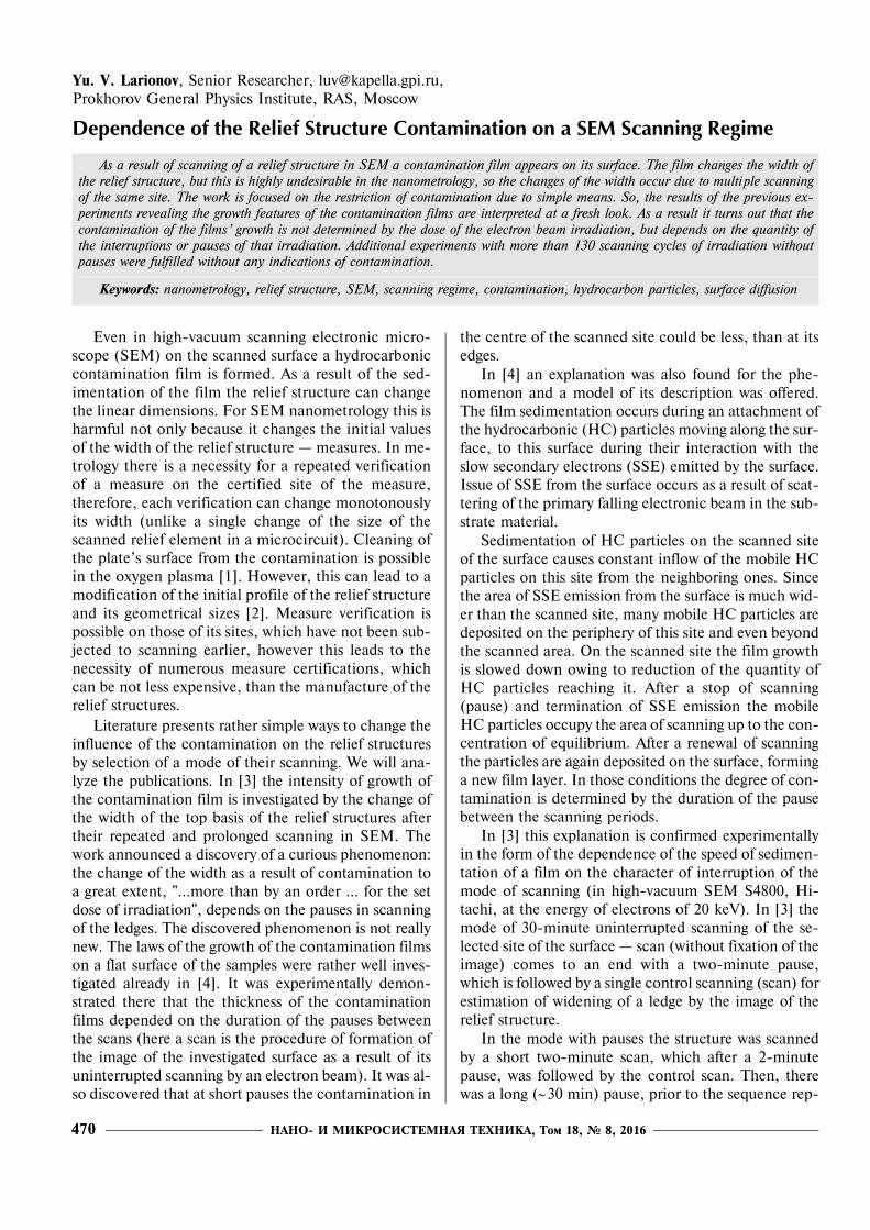
оøибки в работе [3] преäставëено на рис. 2. На неìпривеäены те же äанные изìенения øирины вер-хнеãо основания (W ) реëüефной структуры в хоäеобëу÷ения, ÷то и в [3], но в зависиìости не от äозыобëу÷ения, а от ÷исëа прерываний сканирований впрерывистоì и непрерывноì режиìах. Из рис. 1
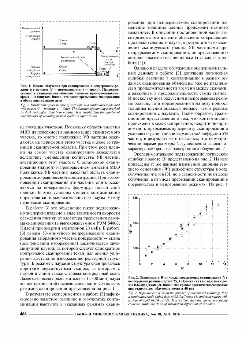
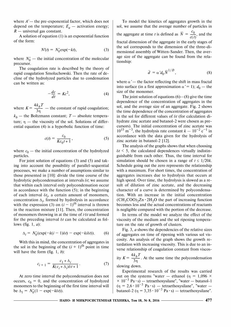
Рис. 1. Циклы облучения при сканировании в непрерывном ре-жиме и с паузами (I � интенсивность; t � время). Продолжи-тельность сканирования помечена темными прямоугольниками,время � в минутах. Видно, что число прерываний сканированияв обоих циклах равно двумFig. 1. Irradiation cycles in case of scanning in a continuous mode andwith pauses (I � intensity, t � time). The duration of scanning is markedby dark rectangles, time is in minutes. It is visible, that the number ofinterruptions of scanning in both cycles is equal to two
Рис. 2. Зависимости W от числа прерываемых сканирований N внепрерывном режиме с дозой 25,3 нКл/скан (1) и с паузами с до-зой 0,62 нКл/скан (2). Видно, что кривые практически совпадаютпри отличии доз облучения почти в 40 разFig. 2. Dependences of W on the number of interrupted scannings N ina continuous mode with a dose of 25,3 nC/scan (1) and with pauses witha dose of 0,62 nC/skan (2). It is visible, that the curves practicallycoincide, while the doses of irradiation differ almost 40 times
НАНО- И МИКРОСИСТЕМНАЯ ТЕХНИКА, Том 18, № 8, 2016 469
виäно, ÷то ÷исëо прерываний в обоих режиìахсканирования оäинаково.Как виäно, кривые по÷ти совпаäаþт при разëи-
÷ии äоз обëу÷ения на оäно сканирование äëя нихпо÷ти в 40 раз. Это äоказывает, ÷то вëияþщей ве-ëи÷иной явëяется не äоза обëу÷ения, а ÷исëо пре-рываний.Из преäставëенноãо экспериìента сëеäует так-
же, ÷то поверхностная äиффузия УВ ÷астиö про-исхоäит относитеëüно быстро, заверøаясü за 2 ìинпосëе окон÷ания сканирования и äо на÷аëа сëе-äуþщеãо периоäа обëу÷ения. Из бëизости кривыхна рис. 2 становится ясно, ÷то за это вреìя УВ÷астиöы успеваþт засеëитü всþ обëастü сканиро-вания äо равновесной пëотности поверхностнойконöентраöии. Поэтоìу преäставëение о тоì, ÷торазный уровенü контаìинаöии при разëи÷ных ре-жиìах сканирования объясняется разной поëно-той запоëнения зоны сканирования УВ ÷астиöа-ìи всëеäствие разной проäоëжитеëüности пауз(÷то утвержäается при описании постаново÷ной÷асти экспериìента в [3]), не соответствует äейс-твитеëüности.Важныì вывоäоì из заново обсужäенноãо экс-
периìента сëеäует то, ÷то äаже äëитеëüное ска-нирование структуры в высоковоëüтноì РЭМ безнаëи÷ия пауз ìожет не привоäитü к контаìина-öии ее поверхности. Этот вывоä поäтвержäен наìив äопоëнитеëüных экспериìентах.
Эксперимент
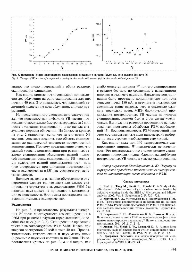
На рис. 3, а преäставëены резуëüтаты изìере-ния W посëе ìноãократноãо еãо сканирования вРЭМ при режиìе с паузаìи (прерыванияìи) и во-обще без пауз (рис. 3, б). Сканирование провоäиëитакже в высоковакууìноì РЭМ S4800 Hitachi приэнерãии эëектронов 20 кэВ и токе 40 пА. Проäоë-житеëüностü кажäоãо скана и пауз ìежäу ниìи(в режиìе с паузаìи) составëяëа по 2 ìин. Из со-поставëения кривых на рис. 3, а и б виäно, как
сëабо ìеняется øирина W при еãо сканированиив режиìе без пауз по сравнениþ с изìененияìиøирины в режиìе с паузаìи. Навеäение контаìи-наöии быëо провеäено äопоëнитеëüно при токеэìиссии пу÷ка 180 нА, и резуëüтаты поäтверäиëисäеëанные выøе вывоäы, ÷еãо и сëеäоваëо ожи-äатü, поскоëüку поток МВЭ, бëокируþщий про-äвижение поверхностных УВ ÷астиö на у÷астоксканирования, äоëжен быë в этоì сëу÷ае увеëи-÷итüся. Вы÷исëение разìеров провоäиëи с испоëü-зованиеì проãраììы обработки РЭМ-изображе-ний [5]. Воспроизвоäиìостü РЭМ-изìерений приэтоì составëяëа äесятые äоëи наноìетра (в выбор-ке по всеì строкаì изображения структуры).Как виäно, äаже при 140 непрерываеìых ска-
нированиях øирина W практи÷ески не изìени-ëасü. Это поäтвержäает, ÷то в такоì режиìе скани-рования происхоäит поëная бëокировка äиффузииповерхностных УВ ÷астиö к у÷астку сканирования.
Автор выражает благодарность А. Ю. Озерину заскрупулезное проведение многочисленных эксперимен-тов по контаминации тест-объектов в РЭМ.
Список литературы
1. Neal S., Tung M., Scott B., Ronald V. A Study of theeffectiveness of the removal of gydrocarbon contamination byoxidative cleaning inside the SEM // Microscopy and Micro-analysis. 2002. Vol. 8. Supplement 2. Р. 720�721.
2. Михуткин А. А., Митюхляев В. Б. Баймухаметов Т. М.и äр. Трехìерная реконструкöия поверхности по äанныìРЭМ // ХIX Росcийский сиìпозиуì по РЭМ и анаëити÷ес-киì ìетоäаì иссëеäований: тезисы äокëаäов. Черноãоëов-ка. С. 320.
3. Гавриленко В. П., Митюхляев В. Б., Раков А. В. и äр.Вëияние контаìинаöии в РЭМ на профиëü реëüефных эëе-ìентов наноìетровоãо äиапазона // Нано- и ìикросистеì-ная техника. 2011. № 2. С. 2�6.
4. Amman M., Sleigh J. W., Lombardi D. R. Atomic forcemicroscopy study of electron beam written contamination struc-ture // J. Vac. Sci. Technol. B. 1996. N. 14 (1). P. 54�62.
5. Программа обработки и анаëиза изображений ìик-роскопов, проãраììная пëатфорìа NDPL. 2009. URL:https://yadi.sk/i/YtOL8GEid9nK4.
Рис. 3. Изменение W при многократном сканировании в режиме с паузами (а),то же, но в режиме без пауз (b)Fig. 3. Change of W in case of a repeated scanning in the mode with pauses (a), in the mode without pauses (b)
НАНО- И МИКРОСИСТЕМНАЯ ТЕХНИКА, Том 18, № 8, 2016470
Yu. V. Larionov, Senior Researcher, [email protected], Prokhorov General Physics Institute, RAS, Moscow
Dependence of the Relief Structure Contamination on a SEM Scanning Regime
Even in high-vacuum scanning electronic micro-scope (SEМ) on the scanned surface a hydrocarboniccontamination film is formed. As a result of the sed-imentation of the film the relief structure can changethe linear dimensions. For SEM nanometrology this isharmful not only because it changes the initial valuesof the width of the relief structure � measures. In me-trology there is a necessity for a repeated verificationof a measure on the certified site of the measure,therefore, each verification can change monotonouslyits width (unlike a single change of the size of thescanned relief element in a microcircuit). Cleaning ofthe plate�s surface from the contamination is possiblein the oxygen plasma [1]. However, this can lead to amodification of the initial profile of the relief structureand its geometrical sizes [2]. Measure verification ispossible on those of its sites, which have not been sub-jected to scanning earlier, however this leads to thenecessity of numerous measure certifications, whichcan be not less expensive, than the manufacture of therelief structures.
Literature presents rather simple ways to change theinfluence of the contamination on the relief structuresby selection of a mode of their scanning. We will ana-lyze the publications. In [3] the intensity of growth ofthe contamination film is investigated by the change ofthe width of the top basis of the relief structures aftertheir repeated and prolonged scanning in SEМ. Thework announced a discovery of a curious phenomenon:the change of the width as a result of contamination toa great extent, "...more than by an order ... for the setdose of irradiation", depends on the pauses in scanningof the ledges. The discovered phenomenon is not reallynew. The laws of the growth of the contamination filmson a flat surface of the samples were rather well inves-tigated already in [4]. It was experimentally demon-strated there that the thickness of the contaminationfilms depended on the duration of the pauses betweenthe scans (here a scan is the procedure of formation ofthe image of the investigated surface as a result of itsuninterrupted scanning by an electron beam). It was al-so discovered that at short pauses the contamination in
the centre of the scanned site could be less, than at itsedges.
In [4] an explanation was also found for the phe-nomenon and a model of its description was offered.The film sedimentation occurs during an attachment ofthe hydrocarbonic (HC) particles moving along the sur-face, to this surface during their interaction with theslow secondary electrons (SSE) emitted by the surface.Issue of SSE from the surface occurs as a result of scat-tering of the primary falling electronic beam in the sub-strate material.
Sedimentation of HC particles on the scanned siteof the surface causes constant inflow of the mobile HCparticles on this site from the neighboring ones. Sincethe area of SSE emission from the surface is much wid-er than the scanned site, many mobile HC particles aredeposited on the periphery of this site and even beyondthe scanned area. On the scanned site the film growthis slowed down owing to reduction of the quantity ofHC particles reaching it. After a stop of scanning(pause) and termination of SSE emission the mobileHC particles occupy the area of scanning up to the con-centration of equilibrium. After a renewal of scanningthe particles are again deposited on the surface, forminga new film layer. In those conditions the degree of con-tamination is determined by the duration of the pausebetween the scanning periods.
In [3] this explanation is confirmed experimentallyin the form of the dependence of the speed of sedimen-tation of a film on the character of interruption of themode of scanning (in high-vacuum SEМ S4800, Hi-tachi, at the energy of electrons of 20 keV). In [3] themode of 30-minute uninterrupted scanning of the se-lected site of the surface � scan (without fixation of theimage) comes to an end with a two-minute pause,which is followed by a single control scanning (scan) forestimation of widening of a ledge by the image of therelief structure.
In the mode with pauses the structure was scannedby a short two-minute scan, which after a 2-minutepause, was followed by the control scan. Then, therewas a long (∼30 min) pause, prior to the sequence rep-
As a result of scanning of a relief structure in SEM a contamination film appears on its surface. The film changes the width ofthe relief structure, but this is highly undesirable in the nanometrology, so the changes of the width occur due to multiple scanningof the same site. The work is focused on the restriction of contamination due to simple means. So, the results of the previous ex-periments revealing the growth features of the contamination films are interpreted at a fresh look. As a result it turns out that thecontamination of the films� growth is not determined by the dose of the electron beam irradiation, but depends on the quantity ofthe interruptions or pauses of that irradiation. Additional experiments with more than 130 scanning cycles of irradiation withoutpauses were fulfilled without any indications of contamination.
Keywords: nanometrology, relief structure, SEM, scanning regime, contamination, hydrocarbon particles, surface diffusion
НАНО- И МИКРОСИСТЕМНАЯ ТЕХНИКА, Том 18, № 8, 2016 471
etition. The scheme of the modes of scanning is pre-sented in fig. 1.
As a result of the experiments in [3] an appreciabledistinction was recorded in the results of contaminationof the ledges in the specified modes of scanning: duringan uninterrupted scanning the change of the thicknessof a film occurred much more slowly. In the descriptionof the production part of the experiment this phenom-enon was explained by the reduction of the duration ofa pause, due to which, according to the authors, occu-pation of the scanned site by HC particles during an un-interrupted scanning appeared to be incomplete, justlike in [4].
However, in the section of discussion in [3] a logicalerror was made: the distinctions in contamination indifferent modes of scanning were already explained notby the differences in duration of time between thescans, but by distinctions in the durations of the scans.Since in a continuous mode the irradiation dose ismore, the norm of the gain of the film thickness per adose appeares less, than in the mode of scanning withpauses. Then the traditional opinion that the contam-ination occurs during scanning was noncritically ap-plied to the interrupted version of scanning in the con-ditions of restriction of the surface diffusion of the HCparticles. As a result, it turned out that the geometricalparameters of a measure "...essentially depend on thecharacter of accumulation of the dose of electronic ir-radiation...".
An experimental proof of the logical error in [3] ispresented in fig. 2. It presents the same changes of thewidth of the top basis W of the relief structure duringirradiation, as given in [3], but in dependence not onthe irradiation dose, but on the number of interruptionsof scannings in the interrupted and continuous modes.In fig. 1 it is visible, that the number of interruptions inboth modes of scanning is identical. The curves almostcoincide, while for them there is a difference of almost40 times in the doses of irradiation per one scanning.This proves that the influencing value is not the irradi-ation dose, but the number of interruptions.
From the experiment it also follows, that the surfacediffusion of the HC particles occurs rather quickly,coming to the end in 2 min after termination of scan-ning and prior to the beginning of the next period of ir-radiation. From the affinity of the curves in fig. 2 it isclear, that in this period the HC particles manage to oc-cupy all the scanning area up to the equilibrium densityof the surface concentration. Therefore, the idea thatdifferent levels of contamination at various modes ofscanning are explained by different completeness of fill-ing of the zone of scanning by the HC particles owingto different duration of pauses (as the description of theproduction part of the experiment in [3] says), does notcorrespond to reality.
An important conclusion from the discussed exper-iment is that even a prolonged scanning of the structurein a high-voltage SEМ without pauses may not lead tocontamination of the surface of this structure. This con-clusion was confirmed by our additional experiments.
Experiment
Fig. 3, а presents the results of measurement W asa result of its multiple scanning in SEM in the modewith pauses (interruptions) and without any pauses(fig. 3, b). Scanning was also done in high-vacuumSEM S4800 Hitachi at the energy of electrons of 20 keVand current of 40 pA. The duration of every scan andpauses between them (in the mode with pauses) was2 min. Comparison of the curves in fig. 3, a and bshows, how little the ledge width changes at its scanningin the mode without pauses compared with the meas-urements of the width in the mode with pauses. In-duction of contamination was additionally done at thecurrent emission of beam of 180 nA, and, as it was ex-pected, the results confirmed the drawn conclusions,because in this case the flow of SSE blocking the ad-vancement of the surface HC particles to the site ofscanning should have increased. Calculation of the di-mensions was done with the use of the program forprocessing of SEM images [5]. At that, the reproduci-bility of the SEМ measurements was equal to the tenthshares of a nanometer (in sampling in all the lines of theimage of the structure).
As one can see, even in case of 140 uninterruptedscannings the width W practically did not change. Thisproves that in this mode of scanning a full blocking ofthe diffusion of the surface HC particles to the scanningsite takes place.
The author expresses his gratitude to A. J. Ozerin forthe scrupulous and numerous experiments concerning thecontamination of the test-objects in SEМ.
References
1. Neal S., Tung M., Scott B., Ronald V. A Study of the ef-fectiveness of the removal of gydrocarbon contamination by ox-idative cleaning inside the SEM, Microscopy and Microanalysis,2002, vol. 8, Supplement 2, pp. 720�721.
2. Mikhutkin A. A., Mit`ukhlyaev V. B., Baimukhamedov T. M.et al. Trekh-mernaya rekonstuctsiya po dannym REM, ХIX Rus.Symposium po REM and analyticheskim metodam issledovanii.Chernogolovka. Tesisi, p. 320.
3. Gavrilenko V. P., Mit`ukhlyaev V. B., Rakov A. V. et al.,Vliyanie kontaminatsii v REM na profil rel`efnoi strukturi v na-nometrovom diapazone, Nano and mikrosistemnaya tekhnika,2011, no. 2, pp. 2�6.
4. Amman M., Sleigh J. W., Lombardi D. R. Atomic forcemicroscopy study of electron beam written contamination struc-ture, J. Vac. Sci. Technol. B., 1996, no. 14 (1), pp. 54�62.
5. Programma obrabotki i analiza izobragenii mikroskopov,programnaya platforma NDPL. 2009. URL: https://yadi.sk/i/YtOL8GEid9nK4.
НАНО- И МИКРОСИСТЕМНАЯ ТЕХНИКА, Том 18, № 8, 2016472
УДК 6-022.532
И. А. Пронин 1, канä. техн. наук, äоö., e-mail: [email protected]; Н. Д. Якушова1, аспирант, А. А. Карманов1, ст. препоäаватеëü, И. А. Аверин1, д-р техн. наук, проф., зав. каф., В. А. Мошников2,3, ä-р физ.-ìат. наук, проф.1 Пензенский ãосуäарственный университет (ã. Пенза, Россия)2 Санкт-Петербурãский ãосуäарственный эëектротехни÷еский университет "ЛЭТИ" иì. В. И. Уëüянова (Ленина) (ã. Санкт-Петербурã, Россия)3 Санкт-Петербурãский поëитехни÷еский университет Петра Веëикоãо
ÌÎÄÅËÜ ÑÁÎÐÊÈ ÍÀÍÎÊÎÌÏÎÇÈÒÍÛÕ È ÈÅÐÀÐÕÈ×ÅÑÊÈÕ ÍÀÍÎÑÒÐÓÊÒÓÐ Â ÇÎËÜ-ÃÅËÜ-ÏÐÎÖÅÑÑÀÕ
Совреìенные принöипы ìатериаëовеäения ха-рактеризуþтся теì, ÷то ìатериаëы с необы÷ны-ìи свойстваìи ìожно сфорìироватü из наноэëе-ìентов, собранных в иерархи÷еские структуры, апри этоì саìи наноэëеìенты ìоãут иìетü раз-ëи÷нуþ прироäу: бытü кристаëëи÷ескиìи, аìорф-ныìи, фрактаëüныìи [1]. Свойства таких объектовзависят от усëовий роста и эвоëþöии, а наносис-теìы ìоãут отëи÷атüся иерархией, связываþщиìикоìпозитаìи, наноструктурой интерфейсных об-ëастей ìежäу ÷астиöаìи. Развитие такоãо ìатериа-ëовеä÷ескоãо поäхоäа, несìотря на зна÷итеëüныеуспехи за посëеäние ãоäы, соäержит ìноãо нераз-реøенных заäа÷ в обëасти синтеза нано÷астиö,сборки из них наносистеì, их äиаãностики и при-борных реаëизаöий. Из нау÷ных пробëеì прежäевсеãо необхоäиìо выäеëитü ìоäеëüные преäстав-ëения, в которых скрытые параìетры ìоãут при-воäитü к преäсказаниþ особенностей поëу÷ениянаноэëеìентов и появëения новых кооперативныхсвойств. Поэтоìу öеëüþ работы явиëасü разра-ботка физико-хиìи÷еских ìоäеëей созäания нано-коìпозитных и иерархи÷еских структур äëя раз-ëи÷ных техни÷еских приìенений в раìках зоëü-ãеëü-ìетоäа.
Проìоäеëируеì форìирование коëëоиäных÷астиö оксиäа öинка на ранних этапах созреваниязоëей. Буäеì с÷итатü, ÷то в этоì сëу÷ае сборка ÷ас-тиö описывается в раìках ìоäеëи äиффузионно-ëиìитированной аãреãаöии (DLA), проäуктоì ко-торой явëяется аãреãат Виттена�Санäера с фрак-таëüной разìерностüþ D. В раìках ìоäеëи Виттенаи Санäера разработана проãраììа [2] визуаëиза-öии роста аãреãата. Рост кëастера происхоäиë зас÷ет сëу÷айноãо бëужäания ÷астиö, выпущенных сокружности раäиусоì R1, на кваäратной реøетке и
посëеäуþщеãо их прикрепëения в сëу÷ае касания скëастероì. В резуëüтате, посëе ìноãократноãо по-вторения äанноãо проöесса форìируется фрактаëü-ный аãреãат, ÷исëо ÷астиö Nf в котороì связано с
раäиусоì инерöии Rg выражениеì Nf = ς , ãäе
ς � префактор; a0 � разìер ìоноìера. На боëее
позäних этапах созревания преиìущественно осу-ществëяется кëастер-кëастерная аãреãаöия [3] спроäоëжаþщиìся проöессоì "кëастер�÷астиöа"[4], при которой ÷астиöы, образовавøиеся на пер-воì этапе, форìируþт иерархи÷ескуþ структуру.
Поступила в редакцию 03.02.2016 г.
Разработана упрощенная модель с небольшим набором характеристических эффективных параметров, позволяющаяадекватно описать рост наночастиц в золях. Эффективные параметры зависят от совокупности технологических фак-торов и, как правило, являются скрытыми, но тенденция их изменения позволяет реализовывать предсказательные функ-ции модели.
Ключевые слова: золь-гель-технология, наноматериалы, поликонденсация, материалы с иерархической структурой
ÌÀÒÅÐÈÀËÎÂÅÄ×ÅÑÊÈÅÈ ÒÅÕÍÎËÎÃÈ×ÅÑÊÈÅ ÎÑÍÎÂÛ ÌÍÑÒ
SCIENCE OF MATERIALSAND TECHNOLOGICAL BASICS OF MNST
Rg
a0----
⎝ ⎠⎜ ⎟⎛ ⎞
D
НАНО- И МИКРОСИСТЕМНАЯ ТЕХНИКА, Том 18, № 8, 2016 473
Эвоëþöия роста ìожет привоäитü к структураìперкоëяöионноãо типа [5], но ÷аще форìируþтсяëабиринтные структуры всëеäствие спиноäаëüноãораспаäа [6].Матеìати÷еское ìоäеëирование проöессов ãиä-
роëиза и поëиконäенсаöии в зоëях äостато÷нозатруäнено, поскоëüку ãиäроëити÷еская поëикон-äенсаöия явëяется сëожныì параëëеëüно-посëе-äоватеëüныì проöессоì, ìноãие стаäии которо-ãо, особенно ранние, обратиìы, наприìер, за с÷етпротекания реэтерификаöии и аëкоãоëиза [7, 8].Поэтоìу воспоëüзуеìся поäхоäоì, преäëоженныìв работе [9]. Упрощенно буäеì с÷итатü, ÷то ско-ростü убыëи конöентраöии ìоëекуëярных прекур-
соров � � реакöия псевäопервоãо поряäка, т.е.
� = kN', (1)
ãäе k � константа скорости реакöии ãиäроëиза. Еезависиìостü от теìпературы ìожно преäставитü ввиäе уравнения Аррениуса:
k = A' exp , (2)
ãäе A' � преäэкспоненöиаëüный ìножитеëü, не за-висящий от теìпературы; Ea � энерãия активаöии;R � универсаëüная ãазовая постоянная.Реøениеì уравнения (1) явëяется экспоненöи-
аëüная функöия виäа:
N'(t) = exp(�kt), (3)
ãäе � на÷аëüная конöентраöия ìоëекуëярноãопрекурсора.Скоростü коаãуëяöии описывается в раìках те-
ории быстрой коаãуëяöии Сìоëуховскоãо. Тоãäаскоростü убыëи ãиäроëизовавøихся ÷астиö за с÷ет
проöессов поëиконäенсаöии � ìожно записатü
в сëеäуþщеì виäе:
� = Kc2, (4)
ãäе K = � константа быст-
рой коаãуëяöии; kb � постоянная
Боëüöìана; T � абсоëþтная теì-пература; η � вязкостü зоëя. Реøе-ниеì äифференöиаëüноãо уравне-ния (4) явëяется ãипербоëи÷ескаяфункöия вреìени:
c(t) = , (5)
ãäе c0 � на÷аëüная конöентраöия ãиäроëизовав-øихся ÷астиö.Дëя совìестноãо реøения уравнений (3) и (5) и
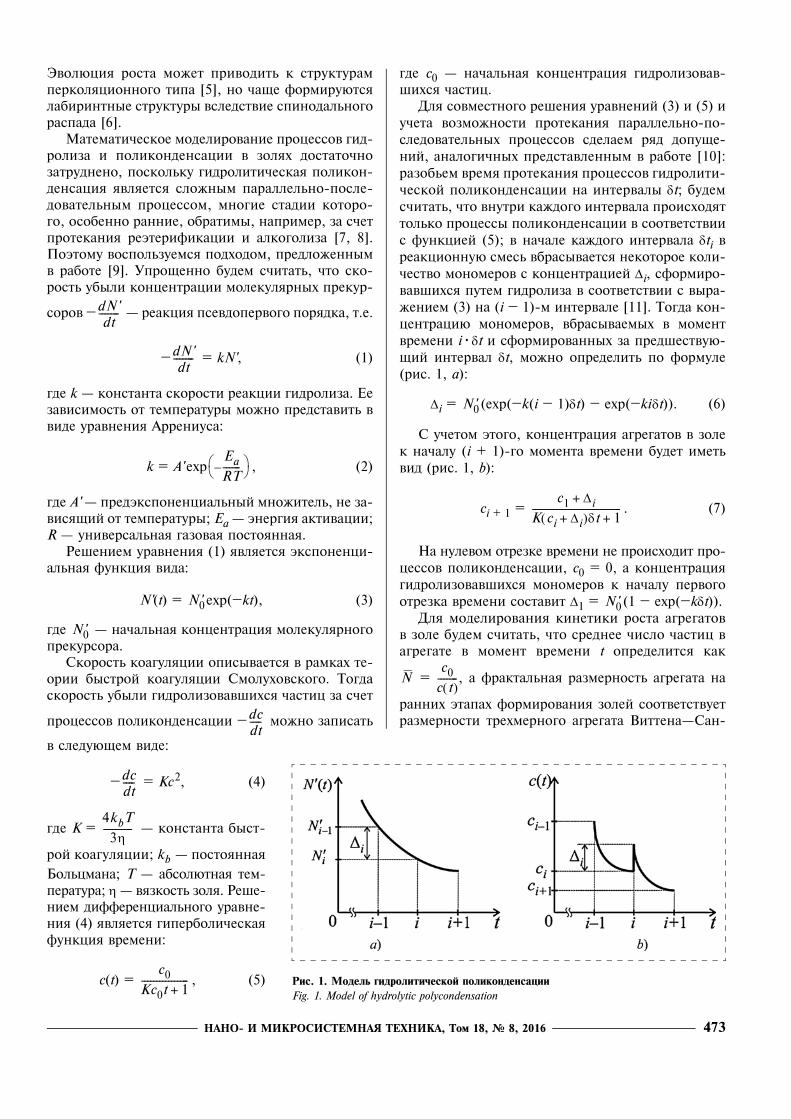
у÷ета возìожности протекания параëëеëüно-по-сëеäоватеëüных проöессов сäеëаеì ряä äопуще-ний, анаëоãи÷ных преäставëенныì в работе [10]:разобüеì вреìя протекания проöессов ãиäроëити-÷еской поëиконäенсаöии на интерваëы δt; буäеìс÷итатü, ÷то внутри кажäоãо интерваëа происхоäяттоëüко проöессы поëиконäенсаöии в соответствиис функöией (5); в на÷аëе кажäоãо интерваëа δti вреакöионнуþ сìесü вбрасывается некоторое коëи-÷ество ìоноìеров с конöентраöией Δi, сфорìиро-вавøихся путеì ãиäроëиза в соответствии с выра-жениеì (3) на (i � 1)-ì интерваëе [11]. Тоãäа кон-öентраöиþ ìоноìеров, вбрасываеìых в ìоìентвреìени i�δt и сфорìированных за преäøествуþ-щий интерваë δt, ìожно опреäеëитü по форìуëе(рис. 1, a):
Δi = (exp(�k(i � 1)δt) � exp(�kiδt)). (6)
С у÷етоì этоãо, конöентраöия аãреãатов в зоëек на÷аëу (i + 1)-ãо ìоìента вреìени буäет иìетüвиä (рис. 1, b):
ci + 1 = . (7)
На нуëевоì отрезке вреìени не происхоäит про-öессов поëиконäенсаöии, c0 = 0, а конöентраöияãиäроëизовавøихся ìоноìеров к на÷аëу первоãоотрезка вреìени составит Δ1 = (1 � exp(�kδt)).Дëя ìоäеëирования кинетики роста аãреãатов
в зоëе буäеì с÷итатü, ÷то среäнее ÷исëо ÷астиö ваãреãате в ìоìент вреìени t опреäеëится как
= , а фрактаëüная разìерностü аãреãата на
ранних этапах форìирования зоëей соответствуетразìерности трехìерноãо аãреãата Виттена�Сан-
dN'dt
-------
dN'dt
-------
Ea
RT------–⎝ ⎠
⎛ ⎞
N0'
N0'
dcdt----
dcdt----
4kbT
3η----------
c0
Kc0t 1+----------------
N0'
c1 Δi+
K ci Δi+( )δt 1+------------------------------
N0'
Nc0
c t( )-------
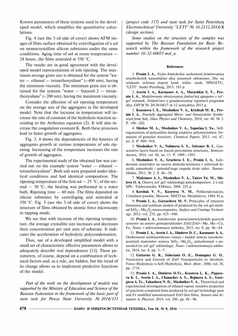
Рис. 1. Модель гидролитической поликонденсацииFig. 1. Model of hydrolytic polycondensation
НАНО- И МИКРОСИСТЕМНАЯ ТЕХНИКА, Том 18, № 8, 2016474
äера. Тоãäа среäний разìер аãреãата ìожно най-ти из соотноøения:
= α'd0 , (8)
ãäе α' � коэффиöиент, отражаþщий перехоä ìас-совоãо фрактаëа в поверхностный (в первоì при-бëижении α' = 1); d0 � разìер ìоноìера.Совìестное ÷исëенное реøение уравнений
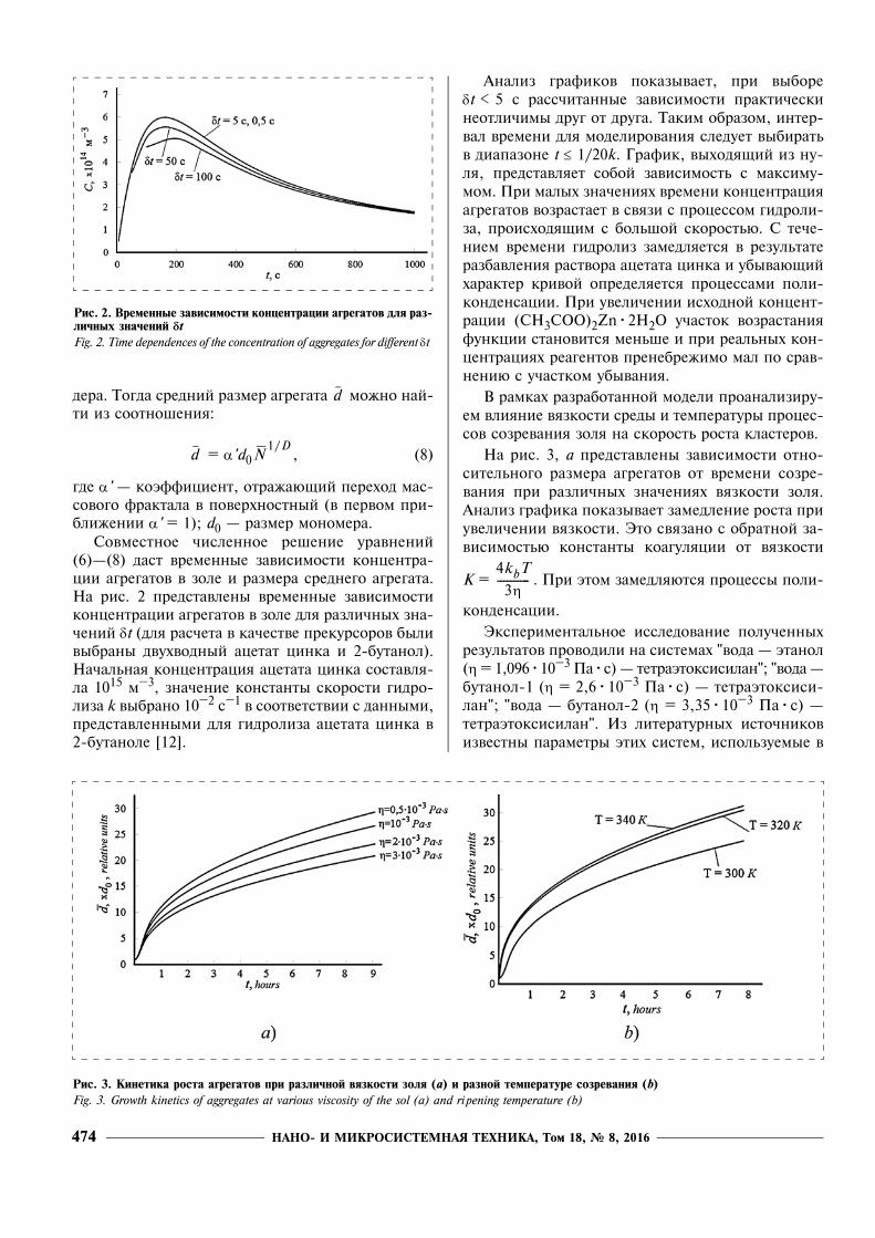
(6)�(8) äаст вреìенные зависиìости конöентра-öии аãреãатов в зоëе и разìера среäнеãо аãреãата.На рис. 2 преäставëены вреìенные зависиìостиконöентраöии аãреãатов в зоëе äëя разëи÷ных зна-÷ений δt (äëя рас÷ета в ка÷естве прекурсоров быëивыбраны äвухвоäный аöетат öинка и 2-бутаноë).На÷аëüная конöентраöия аöетата öинка составëя-ëа 1015 ì�3, зна÷ение константы скорости ãиäро-ëиза k выбрано 10�2 c�1 в соответствии с äанныìи,преäставëенныìи äëя ãиäроëиза аöетата öинка в2-бутаноëе [12].
Анаëиз ãрафиков показывает, при выбореδt < 5 с расс÷итанные зависиìости практи÷ескинеотëи÷иìы äруã от äруãа. Такиì образоì, интер-ваë вреìени äëя ìоäеëирования сëеäует выбиратüв äиапазоне t ≤ 1/20k. График, выхоäящий из ну-ëя, преäставëяет собой зависиìостü с ìаксиìу-ìоì. При ìаëых зна÷ениях вреìени конöентраöияаãреãатов возрастает в связи с проöессоì ãиäроëи-за, происхоäящиì с боëüøой скоростüþ. С те÷е-ниеì вреìени ãиäроëиз заìеäëяется в резуëüтатеразбавëения раствора аöетата öинка и убываþщийхарактер кривой опреäеëяется проöессаìи поëи-конäенсаöии. При увеëи÷ении исхоäной конöент-раöии (CH3COO)2Zn�2H2O у÷асток возрастанияфункöии становится ìенüøе и при реаëüных кон-öентраöиях реаãентов пренебрежиìо ìаë по срав-нениþ с у÷асткоì убывания.В раìках разработанной ìоäеëи проанаëизиру-
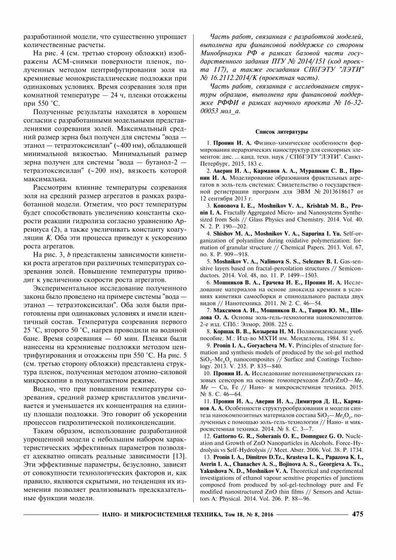
еì вëияние вязкости среäы и теìпературы проöес-сов созревания зоëя на скоростü роста кëастеров.На рис. 3, a преäставëены зависиìости отно-
ситеëüноãо разìера аãреãатов от вреìени созре-вания при разëи÷ных зна÷ениях вязкости зоëя.Анаëиз ãрафика показывает заìеäëение роста приувеëи÷ении вязкости. Это связано с обратной за-висиìостüþ константы коаãуëяöии от вязкости
K = . При этоì заìеäëяþтся проöессы поëи-
конäенсаöии.Экспериìентаëüное иссëеäование поëу÷енных
резуëüтатов провоäиëи на систеìах "воäа � этаноë(η = 1,096�10�3 Па�с) � тетраэтоксисиëан"; "воäа �бутаноë-1 (η = 2,6�10�3 Па�с) � тетраэтоксиси-ëан"; "воäа � бутаноë-2 (η = 3,35�10�3 Па�с) �тетраэтоксисиëан". Из ëитературных исто÷никовизвестны параìетры этих систеì, испоëüзуеìые в
d
d N1/D
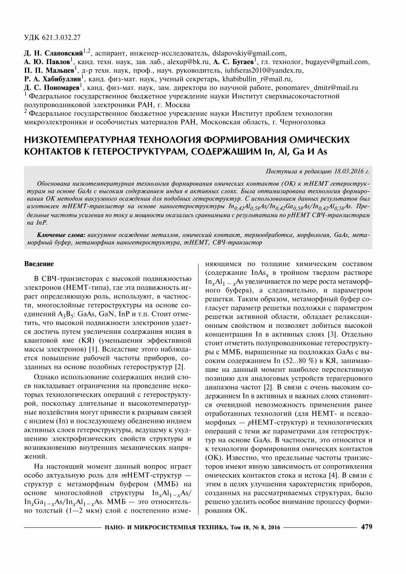
Рис. 2. Временные зависимости концентрации агрегатов для раз-личных значений dtFig. 2. Time dependences of the concentration of aggregates for different δt
Рис. 3. Кинетика роста агрегатов при различной вязкости золя (a) и разной температуре созревания (b)Fig. 3. Growth kinetics of aggregates at various viscosity of the sol (a) and ripening temperature (b)
4kbT
3η----------
НАНО- И МИКРОСИСТЕМНАЯ ТЕХНИКА, Том 18, № 8, 2016 475
разработанной ìоäеëи, ÷то существенно упрощаеткоëи÷ественные рас÷еты.На рис. 4 (сì. третüþ сторону обëожки) изоб-
ражены АСМ-сниìки поверхности пëенок, по-ëу÷енных ìетоäоì öентрифуãирования зоëя накреìниевые ìонокристаëëи÷еские поäëожки приоäинаковых усëовиях. Вреìя созревания зоëя прикоìнатной теìпературе � 24 ÷, пëенки отожженыпри 550 °С.Поëу÷енные резуëüтаты нахоäятся в хороøеì
соãëасии с разработанныìи ìоäеëüныìи преäстав-ëенияìи созревания зоëей. Максиìаëüный среä-ний разìер зерна быë поëу÷ен äëя систеìы "воäа �этаноë � тетраэтоксисиëан" (∼400 нì), обëаäаþщейìиниìаëüной вязкостüþ. Миниìаëüный разìерзерна поëу÷ен äëя систеìы "воäа � бутаноë-2 �тетраэтоксисиëан" (∼200 нì), вязкостü которойìаксиìаëüна.Рассìотриì вëияние теìпературы созревания
зоëя на среäний разìер аãреãатов в раìках разра-ботанной ìоäеëи. Отìетиì, ÷то рост теìпературыбуäет способствоватü увеëи÷ениþ константы ско-рости реакöии ãиäроëиза соãëасно уравнениþ Ар-рениуса (2), а также увеëи÷иватü константу коаãу-ëяöии K. Оба эти проöесса привеäут к ускорениþроста аãреãатов.На рис. 3, b преäставëены зависиìости кинети-
ки роста аãреãатов при разëи÷ных теìпературах со-зревания зоëей. Повыøение теìпературы приво-äит к увеëи÷ениþ скорости роста аãреãатов.Экспериìентаëüное иссëеäование поëу÷енноãо
закона быëо провеäено на приìере систеìы "воäа �этаноë � тетраэтоксисиëан". Оба зоëя быëи при-ãотовëены при оäинаковых усëовиях и иìеëи иäен-ти÷ный состав. Теìпература созревания первоãо25 °С, второãо 50 °С, наãрев провоäиëи на воäянойбане. Вреìя созревания � 60 ìин. Пëенки быëинанесены на креìниевые поäëожки ìетоäоì öен-трифуãирования и отожжены при 550 °С. На рис. 5(сì. третüþ сторону обëожки) преäставëена струк-тура пëенок, поëу÷енная ìетоäоì атоìно-сиëовойìикроскопии в поëуконтактноì режиìе.Виäно, ÷то при повыøении теìпературы со-
зревания, среäний разìер кристаëëитов увеëи÷и-вается и уìенüøается их конöентраöия на еäини-öу пëощаäи поäëожки. Это ãоворит об ускорениипроöессов ãиäроëити÷еской поëиконäенсаöии.Такиì образоì, испоëüзование разработанной
упрощенной ìоäеëи с небоëüøиì набороì харак-теристи÷еских эффективных параìетров позвоëя-ет аäекватно описатü реаëüные зависиìости [13].Эти эффективные параìетры, безусëовно, зависятот совокупности техноëоãи÷еских факторов и, какправиëо, явëяþтся скрытыìи, но тенäенöия их из-ìенения позвоëяет реаëизовыватü преäсказатеëü-ные функöии ìоäеëи.
Часть работ, связанная с разработкой моделей,выполнена при финансовой поддержке со стороныМинобрнауки РФ в рамках базовой части госу-дарственного задания ПГУ № 2014/151 (код проек-та 117), а также госзадания СПбГЭТУ "ЛЭТИ"№ 16.2112.2014/К (проектная часть).
Часть работ, связанная с исследованием струк-туры образцов, выполнена при финансовой поддер-жке РФФИ в рамках научного проекта № 16-32-00053 мол_а.
Список литературы
1. Пронин И. А. Физико-хиìи÷еские особенности фор-ìирования иерархи÷еских наноструктур äëя сенсорных эëе-ìентов: äис. ... канä. техн. наук / СПбГЭТУ "ЛЭТИ". Санкт-Петербурã, 2015, 183 с.
2. Аверин И. А., Карманов А. А., Мурашкин С. В., Про-нин И. А. Моäеëирование образования фрактаëüных аãре-ãатов в зоëü-ãеëü систеìах: Свиäетеëüство о ãосуäарствен-ной реãистраöии проãраìì äëя ЭВМ № 2013618617 от12 сентября 2013 ã.
3. Kononova I. E., Moshnikov V. A., Krishtab M. B., Pro-nin I. A. Fractally Aggregated Micro- and Nanosystems Synthe-sized from Sols // Glass Physics and Chemistry. 2014. Vol. 40.N. 2. P. 190�202.
4. Shishov M. A., Moshnikov V. A., Sapurina I. Yu. Self-or-ganization of polyaniline during oxidative polymerization: for-mation of granular structure // Chemical Papers. 2013. Vol. 67,no. 8. P. 909�918.
5. Moshnikov V. A., Nalimova S. S., Seleznev B. I. Gas-sen-sitive layers based on fractal-percolation structures // Semicon-ductors. 2014. Vol. 48, no. 11. P. 1499�1503.
6. Мошников В. А., Грачева И. Е., Пронин И. А. Иссëе-äование ìатериаëов на основе äиоксиäа креìния в усëо-виях кинетики саìосборки и спиноäаëüноãо распаäа äвухвиäов // Нанотехника. 2011. № 2. С. 46�54.
7. Максимов А. И., Мошников В. А., Таиров Ю. М., Ши-лова О. А. Основы зоëü-ãеëü-техноëоãии нанокоìпозитов.2-е изä. СПб.: Эëìор, 2008. 225 с.
8. Коршак В. В., Козырева Н. М. Поëиконäенсаöия: у÷еб.пособие. М.: Изä-во МХТИ иì. Менäеëеева, 1984. 81 с.
9. Pronin I. A., Goryacheva M. V. Principles of structure for-mation and synthesis models of produced by the sol-gel methodSiO2-MexOy nanocomposites // Surface and Coatings Techno-logy. 2013. V. 235. P. 835�840.10. Пронин И. А. Иссëеäование потенöиоìетри÷еских ãа-зовых сенсоров на основе ãоìоперехоäов ZnO/ZnO�Me,Me � Cu, Fe // Нано- и ìикросистеìная техника. 2015.№ 8. С. 46�64.11. Пронин И. А., Аверин И. А., Димитров Д. Ц., Карма-
нов А. А. Особенности структурообразования и ìоäеëи син-теза нанокоìпозитных ìатериаëов состава SiO2�MexOy, по-ëу÷енных с поìощüþ зоëü-ãеëü-техноëоãии // Нано- и ìик-росистеìная техника. 2014. № 8. С. 3�7.12. Gattorno G. R., Soberanis O. E., Domnguez G. O. Nucle-
ation and Growth of ZnO Nanoparticles in Alcohols. Force-Hy-drolysis vs Self-Hydrolysis // Meet. Abstr. 2006. Vol. 38. P. 1734.13. Pronin I. A., Dimitrov D.Tz., Krasteva L. K., Papazova K. I.,
Averin I. A., Chanachev A. S., Bojinova A. S., Georgieva A. Ts.,Yakushova N. D., Moshnikov V. A. Theoretical and experimentalinvestigations of ethanol vapour sensitive properties of junctionscomposed from produced by sol-gel-technology pure and Femodified nanostructured ZnO thin films // Sensors and Actua-tors A: Physical. 2014. Vol. 206. P. 88�96.
НАНО- И МИКРОСИСТЕМНАЯ ТЕХНИКА, Том 18, № 8, 2016476
I. A. Pronin, PhD., Associate Professor, [email protected], N. D. Yakushova, Postgraduate Student,A. A. Karmanov, Senior Lecturer, Penza State University, I. A. Averin, D. Sc., Professor, Head of Department, V. A. Moshnikov, Professor, St. Petersburg Electrotechnical University-LETI
Assemblage Model of the Nanocomposite and Hierarchical Nanostructuresin the Sol-gel Processes
The material science is characterized by the fact thatthe materials with unusual properties can be formedfrom nanoelements collected in the hierarchical struc-tures, at this, the nanoelements can be of different na-ture: crystalline, amorphous, fractal [1]. The propertiesof objects depend on the conditions of growth and ev-olution, and the nanosystems can differ by hierarchy,linking com-posites, nanostructure of the interfaces be-tween the particles. Development of this approach, de-spite the significant progress, contains a lot of unsolvedproblems in the field of nanoparticle synthesis, assem-bly of these systems, diagnostics and device implemen-tations. First of all, the model representations should beallocated, in which hidden parameters can lead to pre-diction of the features of nanoelements obtainment andthe emergence of new properties. Therefore, the pur-pose of the article is the development of physical-chemical models of nanocomposites and hierarchicalstructures creating for various applications within thesol-gel method.
Let us to model formation of the colloidal particlesof zinc oxide in the early stages of sols ripening. In thiscase, the assembly of particles is described by the modelof diffusion-limited aggregation (DLA), the product ofwhich is the aggregate of Witten-Sander with fractal di-mension D. The program was developed within themodel [2] for imaging of aggregate growth. The in-crease was due to the random walk of particles re-leased from a circle of radius R1 on a square lattice and
their subsequent attachment in the case of contactwith the cluster. After multiple repetitions the fractal
aggregate is generated, the number of particles Nf is
associated with a radius of gyration Rg by the expres-
sion Nf = ς , where ς � prefactor; a0 � a size of
the monomer. Cluster-cluster aggregation occurs inthe later stages of ripening [3], at which the ongoingprocess of "cluster-particle" [4], in which the particlesformed in the first stage form a hierarchical structure.Evolution of growth may lead to a percolation-typestructures [5], but more often the labyrinth structure areformed due to spinodal decomposition [6].
Simulation of hydrolysis and polycondensation inthe sols is quite difficult because the hydrolytic poly-condensation is a difficult parallel-sequential process,many of which stages, especially early, are reversible,for example, by alcoholysis and reesterification [7, 8].Let us use the approach proposed in [9]. Simplistically,we assume that the decrease rate of the concentration
of molecular precursors � � pseudo-first-order re-
action, i.e.,
� = kN', (1)
where k � the rate constant for the hydrolysis reaction.Its dependence on the temperature can be representedby the Arrhenius equation:
k = A' exp , (2)
The article is devoted to modeling, simulation and experimental verification laws of the origin and evolution of single na-noobjects in sols, including the management of their size, concentration and fractal. At the same time highlighted predetermininga pattern that describes the change of concentration of nucleation centers and the decrease in the number of monomers in thesol-gel transition. It has been shown that an adequate descri ption of the real dependencies can be achieved using a simplifiedmodel of a small amount of effective parameters that depend on a combination of technological factors which are typically hiddenbut their tendency changes allow to implement predictive model function. As developed by nucleation model and changes in theconcentration of individual nanoobjects has predictive properties, it can be used effectively to optimize the processes of formationof nanosystems by changing such effective parameters such as the viscosity of the sol and its maturation temperature. Experimentalstudy of the effect of sols ri pening temperature on the evolution and growth of nanoobjects was carried out by the example of thesystem "water � ethanol � tetraethoxysilane". All solutions were prepared under identical conditions and had identical com-position but ri pened at different temperatures. It was found that an increase in the average size of the primary nanoobjects ri peningtemperature increases and, consequently, reduces their concentration per unit area of substrate. An adequate description of theresults has also been achieved by using a simplified model developed, including a small number of variables. These variables ("ef-fective parameters") certainly depend on a combination of technical factors and, as a rule, are hidden, but the trend of changeallows us to implement predictive models functions.
Keywords: sol-gel technology, nanomaterials, polycondensation, materials with hierarchical structure
Rg
a0----
⎝ ⎠⎜ ⎟⎛ ⎞
D
dN'dt
-------
dN'dt
-------
Ea
RT------–⎝ ⎠
⎛ ⎞
НАНО- И МИКРОСИСТЕМНАЯ ТЕХНИКА, Том 18, № 8, 2016 477
where A' � the pre-exponential factor, which does notdepend on the temperature; Ea � activation energy;R � universal gas constant.
A solution of equation (1) is an exponential functionof the form:
N'(t) = exp(�kt), (3)
where � the initial concentration of the molecularprecursor.
The coagulation rate is described by the theory ofrapid coagulation Smoluchowski. Then the rate of de-cline of the hydrolyzed particles due to condensationcan be written as:
� = Kc2, (4)
where K = � the constant of rapid coagulation;
kb � the Boltzmann constant; T � absolute tempera-
ture; η � the viscosity of the sol. Solutions of differ-ential equation (4) is a hyperbolic function of time:
c(t) = , (5)
where c0 � the initial concentration of the hydrolyzedparticles.
For joint solution of equations (3) and (5) and tak-ing into account the possibility of parallel-sequentialprocesses, we make a number of assumptions similar tothose presented in [10]: divide the time course of thehydrolytic polycondensation at intervals δt; we assumethat within each interval only polycondensation occurin accordance with the function (5); in the beginningof each interval δti, a certain amount of monomers,concentration Δi, formed by hydrolysis in accordancewith the expression (3) on (i � 1)th interval is thrownin the reaction mixture [11]. Then, the concentrationof monomers throwing in at the time of i·δt and formedfor the preceding interval δt can be calculated as fol-lows (fig. 1, a):
Δi = (exp(�k(i � 1)δt) � exp(�kiδt)). (6)
With this in mind, the concentration of aggregates inthe sol in the beginning of the (i + 1)th point in timewill have the form (fig. 1, b):
ci + 1 = . (7)
At zero time interval the polycondensation does notoccurs, c0 = 0, and the concentration of hydrolyzedmonomers to the beginning of the first time interval willbe Δ1 = (1 � exp(�kδt)).
To model the kinetics of aggregates growth in thesol, we assume that the average number of particles in
the aggregate at time t is defined as = , and the
fractal dimension of the aggregate in the early stages ofthe sol corresponds to the dimension of the three-di-mensional assembly of Witten-Sander. Then, the aver-age size of the aggregate can be found from the rela-tionship:
= α'd0 , (8)
where α' � the factor reflecting the shift in mass fractalinto surface (in a first approximation α' = 1); d0 � thesize of the monomer.
The joint solution of equations (6)�(8) give the timedependence of the concentration of aggregates in thesol, and the average size of an aggregate. Fig. 2 showsthe time dependence of the concentration of aggregatesin the sol for different values of δt (for calculation di-hydrate zinc acetate and butanol-2 were chosen as pre-cursors). The initial concentration of zinc acetate was1015 m�3, the hydrolysis rate constant k � 10�2 c�1 inaccordance with the data given for the hydrolysis ofzinc acetate in butanol-2 [12].
The analysis of the graphs shows that when choosingδt < 5, the calculated dependences virtually indistin-guishable from each other. Thus, the time interval forsimulation should be chosen in a range of t ≤ 1/20k.Schedule going out the zero represents the relationshipwith a maximum. For short times, the concentration ofaggregates increases due to hydrolysis that occurs athigh speed. Over time, the hydrolysis is slowed as a re-sult of dilution of zinc acetate, and the decreasingcharacter of a curve is determined by polycondensa-tion. With an increase in the initial concentration(CH3COO)2Zn�2H2O the part of increasing functionbecomes less and the actual concentrations of reactantsis negligible compared with the portion of the decrease.
In terms of the model we analyze the effect of theviscosity of the medium and the sol ripening tempera-ture on the rate of growth of clusters.
Fig. 3, a shows the dependencies of the relative sizesof aggregates on time of ripening with various sol vis-cosity. An analysis of the graph shows the growth re-tardation with increasing viscosity. This is due to an in-verse relationship of coagulation constant from viscos-
ity K = . At the same time the polycondensation
slowing down.Experimental research of the results was carried
out on the systems "water � ethanol (η = 1,096 ЅЅ 10�3 Pa�s) � tetraethoxysilane", "water � butanol-1(η = 2,6�10�3 Pa�s) � tetraethoxysilane", "water �butanol-2 (η = 3,35�10�3 Pa�s) � tetraethoxysilane".
N0'
N0'
dcdt----
4kbT
3η----------
c0
Kc0t 1+----------------
N0'
c1 Δi+
K ci Δi+( )δt 1+------------------------------
N0'
Nc0
c t( )-------
d N1/D
4kbT
3η----------
НАНО- И МИКРОСИСТЕМНАЯ ТЕХНИКА, Том 18, № 8, 2016478
Known parameters of these systems used in the devel-oped model, which simplifies the quantitative calcu-lations.
Fig. 4 (see the 3-rd side of cover) shows AFM im-ages of films surface obtained by centrifugation of a solon monocrystalline silicon substrates under the sameconditions. Aging time of sol at room temperature �24 hours, the films annealed at 550 °C.
The results are in good agreement with the devel-oped model representations of sols ripening. The max-imum average grain size is obtained for the system "wa-ter � ethanol � tetraethoxysilane" (∼400 nm), havingthe minimum viscosity. The minimum grain size is ob-tained for the systems "water � butanol-2 � tetrae-thoxysilane" (∼200 nm), having the maximum viscosity.
Consider the affection of sol ripening temperatureon the average size of the aggregates in the developedmodel. Note that the increase in temperature will in-crease the rate of constant of the hydrolysis reaction ac-cording to the Arrhenius equation (2). It will also in-crease the coagulation constant K. Both these processeslead to faster growth of aggregates.
Fig. 3, b shows the dependencies of the kinetics ofaggregates growth at various temperatures of sols rip-ening. Increasing of the temperature increases the rateof growth of aggregates.
The experimental study of the obtained law was car-ried out on the example system "water � ethanol �tetraethoxysilane". Both sols were prepared under iden-tical conditions and had identical composition. Theripening temperature of the first sol � 25 °C, of the sec-ond � 50 °C, the heating was performed in a waterbath. Ripening time � 60 min. The films deposited onsilicon substrates by centrifuging and annealed at550 °C. Fig. 5 (see the 3-rd side of cover) shows thestructure of films obtained by atomic force microscopyin tapping mode.
We see that with increase of the ripening tempera-ture, the average crystallite size increases and decreasestheir concentration per unit area of substrate. It indi-cates the acceleration of hydrolytic polycondensation.
Thus, use of a developed simplified model with asmall set of characteristic effective parameters allows toadequately describe real dependences [13]. These pa-rameters, of course, depend on a combination of tech-nical factors and, as a rule, are hidden, but the trend ofits change allows us to implement predictive functionsof the model.
Part of the work on the development of models wassupported by the Ministry of Education and Science of theRussian Federation in the framework of the basic part ofstate task for Penza State University № 2014/151
(project code 117) and state task for Saint PetersburgElectrotechnical University "LETI" № 16.2112.2014/K(design section).
Some studies on the structure of the samples wassupported by The Russian Foundation for Basic Re-search within the framework of the research projectnumber 16-32-00053 mol_a.
References
1. Pronin I. A., Fiziko-himicheskie osobennosti formirovaniyaierarhicheskih nanostruktur dlya sensornyh ehlementov, Dis. nasoiskanie uchenoj stepeni kand. tekhn. nauk, SPbGETU,"LETI". Sankt-Peterburg, 2015, 183 p.
2. Averin I. A., Karmanov A. A., Murashkin S. V., Pro-nin I. A., Modelirovanie obrazovaniya fraktal'nyj agregatov v zol'-gel' sistemah, Svidetel'stvo o gosudarstvennoj registracii programmdlya EHVM № 2013618617 ot 12 sentyabrya 2013 g.
3. Kononova I. E., Moshnikov V. A., Krishtab M. B., Pro-nin I. A., Fractally Aggregated Micro- and Nanosystems Synthe-sized from Sols, Glass Physics and Chemistry, 2014, var. 40. № 2.P. 190�202.
4. Shishov M. A., Moshnikov V. A., Sapurina I. Yu., Self-organization of polyaniline during oxidative polymerization: for-mation of granular structure, Chemical Papers, 2013, vol. 67,no. 8. P. 909�918.
5. Moshnikov V. A., Nalimova S. S., Seleznev B. I., Gas-sensitive layers based on fractal-percolation structures, Semicon-ductors, 2014, vol. 48, no. 11. P. 1499�1503.
6. Moshnikov V. A., Gracheva I. E., Pronin I. A., Issle-dovanie materialov na osnove dioksida kremniya v usloviyah ki-netiki samosborki i spinodal'nogo raspada dvuh vidov, Nanote-khnika, 2011. № 2. S. 46�54.
7. Maksimov A. I., Moshnikov V. A., Tairov Yu. M., Shi-lova O. A. Osnovy zol'-gel'-tekhnologii nanokompozitov. 2-e izd.SPb.: Tekhnomedia, EHlmor, 2008. 225 p.
8. Korshak V. V., Kozyreva N. M., Polikondensaciya,Uchebnoe posobie, Moscow, MHTI im. Mendeleeva, 1984. 81 p.
9. Pronin I. A., Goryacheva M. V. Principles of structureformation and synthesis models of produced by the sol-gel meth-od SiO2�MexOy nanocomposites, Surface and Coatings Technol-ogy, 2013, vol. 235, pp. 835�840.
10. Pronin I. A., Issledovanie potenciometricheskih gazovyhsensorov na osnove gomoperekhodov ZnO/ZnO�Me, Me�Cu,Fe, Nano- i mikrosistemnaya tekhnika, 2015, no. 8, pp. 46�64.
11. Pronin I. A., Averin I. A., Dimitrov D. C., Karmanov A. A.,Osobennosti strukturoobrazo-vaniya i modeli sinteza nanokom-pozitnyh materialov sostava SiO2�MexOy, poluchennyh s po-moshch'yu zol'-gel' tekhnologii, Nano- i mikrosistemnaya tekhni-ka, 2014, no. 8, pp. 3�7.
12. Gattorno G. R., Soberanis O. E., Domnguez G. O.,Nucleation and Growth of ZnO Nanoparticles in Alcohols.Force-Hydrolysis vs Self-Hydrolysis, Meet. Abstr., 2006, vol. 38,pp. 1734.
13. Pronin I. A., Dimitrov D.Tz., Krasteva L. K., Papazo-va K. I., Averin I. A., Chanachev A. S., Bojinova A. S., Geor-gieva A. Ts., Yakushova N. D., Moshnikov V. A., Theoretical andexperimental investigations of ethanol vapour sensitive propertiesof junctions composed from produced by sol-gel technology pureand Fe modified nanostructured ZnO thin films, Sensors and Ac-tuators A: Physical. 2014, vol. 206, pp. 88�96.
НАНО- И МИКРОСИСТЕМНАЯ ТЕХНИКА, Том 18, № 8, 2016 479
УДК 621.3.032.27
Д. Н. Слаповский1,2, аспирант, инженер-иссëеäоватеëü, [email protected], А. Ю. Павлов1, канä. техн. наук, зав. ëаб., [email protected], А. С. Бугаев1, ãë. техноëоã, [email protected], П. П. Мальцев1, ä-р техн. наук, проф., нау÷. руковоäитеëü, [email protected],Р. А. Хабибуллин1, канä. физ-ìат. наук, у÷еный секретарü, [email protected], Д. С. Пономарев1, канä. физ-ìат. наук, заì. äиректора по нау÷ной работе, [email protected] Феäераëüное ãосуäарственное бþäжетное у÷режäение науки Институт сверхвысоко÷астотной поëупровоäниковой эëектроники РАН, ã. Москва2 Феäераëüное ãосуäарственное бþäжетное у÷режäение науки Институт пробëеì техноëоãии ìикроэëектроники и особо÷истых ìатериаëов РАН, Московская обëастü, ã. Черноãоëовка
ÍÈÇÊÎÒÅÌÏÅÐÀÒÓÐÍÀß ÒÅÕÍÎËÎÃÈß ÔÎÐÌÈÐÎÂÀÍÈß ÎÌÈ×ÅÑÊÈÕ ÊÎÍÒÀÊÒÎÂ Ê ÃÅÒÅÐÎÑÒÐÓÊÒÓÐÀÌ, ÑÎÄÅÐÆÀÙÈÌ In, Al, Ga È As
Введение
В СВЧ-транзисторах с высокой поäвижностüþэëектронов (HEMT-типа), ãäе эта поäвижностü иã-рает опреäеëяþщуþ роëü, испоëüзуþт, в ÷астнос-ти, ìноãосëойные ãетероструктуры на основе со-еäинений A3B5: GaAs, GaN, InP и т.п. Стоит отìе-титü, ÷то высокой поäвижности эëектронов уäает-ся äости÷ü путеì увеëи÷ения соäержания инäия вквантовой яìе (КЯ) (уìенüøения эффективнойìассы эëектронов) [1]. Всëеäствие этоãо набëþäа-ется повыøение рабо÷ей ÷астоты приборов, со-зäанных на основе поäобных ãетероструктур [2].
Оäнако испоëüзование соäержащих инäий сëо-ев накëаäывает оãрани÷ения на провеäение неко-торых техноëоãи÷еских операöий с ãетерострукту-рой, поскоëüку äëитеëüные и высокотеìператур-ные возäействия ìоãут привести к разрываì связейс инäиеì (In) и посëеäуþщеìу обеäнениþ инäиеìактивных сëоев ãетероструктуры, веäущеìу к ухуä-øениþ эëектрофизи÷еских свойств структуры ивозникновениþ внутренних ìехани÷еских напря-жений.
На настоящий ìоìент äанный вопрос иãраетособо актуаëüнуþ роëü äëя mHEMT-структур �структур с ìетаìорфныì буфероì (ММБ) наоснове ìноãосëойной структуры InxAl1�xAs/InxGa1�xAs/InxAl1�xAs. ММБ � это относитеëü-но тоëстый (1�2 ìкì) сëой с постепенно изìе-
няþщиìся по тоëщине хиìи÷ескиì составоì(соäержание InAsx в тройноì тверäоì раствореInxAl1 � xAs увеëи÷ивается по ìере роста ìетаìорф-ноãо буфера), а сëеäоватеëüно, и параìетроìреøетки. Такиì образоì, ìетаìорфный буфер со-ãëасует параìетр реøетки поäëожки с параìетроìреøетки активной обëасти, обëаäает реëаксаöи-онныì свойствоì и позвоëяет äобитüся высокойконöентраöии In в активных сëоях [3]. Отäеëüностоит отìетитü поëупровоäниковые ãетерострукту-ры с ММБ, выращенные на поäëожках GaAs с вы-сокиì соäержаниеì In (52...80 %) в КЯ, заниìаþ-щие на äанный ìоìент наибоëее перспективнуþпозиöиþ äëя анаëоãовых устройств тераãерöовоãоäиапазона ÷астот [2]. В связи с о÷енü высокиì со-äержаниеì In в активных и важных сëоях становит-ся о÷евиäной невозìожностü приìенения ранееотработанных техноëоãий (äëя HEMT- и псевäо-ìорфных � pHEMT-структур) и техноëоãи÷ескихопераöий с теìи же параìетраìи äëя ãетерострук-тур на основе GaAs. В ÷астности, это относится ик техноëоãии форìирования оìи÷еских контактов(ОК). Известно, ÷то преäеëüные ÷астоты транзис-торов иìеþт явнуþ зависиìостü от сопротивëенияоìи÷еских контактов стока и истока [4]. В связи сэтиì в öеëях уëу÷øения характеристик приборов,созäанных на рассìатриваеìых структурах, быëореøено уäеëитü особое вниìание проöессу форìи-рования ОК.
Поступила в редакцию 18.03.2016 г.
Обоснована низкотемпературная технология формирования омических контактов (ОК) к mHEMT гетерострук-турам на основе GaAs c высоким содержанием индия в активных слоях. Была оптимизирована технология формиро-вания ОК методом вакуумного осаждения для подобных гетероструктур. С использованием данных результатов былизготовлен mHEMT-транзистор на основе наногетероструктуры In0,42Al0,58As/In0,42Ga0,58As/In0,42Al0,58As. Пре-
дельные частоты усиления по току и мощности оказались сравнимыми с результатами по pHEMT СВЧ-транзисторамна InP.
Ключевые слова: вакуумное осаждение металлов, омический контакт, термообработка, морфология, GaAs, мета-морфный буфер, метаморфная наногетероструктура, mHEMT, СВЧ-транзистор
НАНО- И МИКРОСИСТЕМНАЯ ТЕХНИКА, Том 18, № 8, 2016480
Основываясü на сказанноì выøе, ëоãи÷ныìстановится искëþ÷итü как ìетоä ионнуþ иìпëан-таöиþ в связи с высокиìи теìператураìи пост-иìпëантаöионноãо отжиãа. Оäниì из возìожныхспособов понизитü теìпературу явëяется ìетоäосажäения в вакууìе при коìнатной теìпературе.В äанной работе рассìатриваþтся проöесс фор-
ìирования ОК ìетоäоì вакууìноãо осажäения äëяmHEMT-ãетероструктур InxAl1�xAs/InxGa1�xAs/InxAl1�xAs и еãо оптиìизаöия.
Эксперимент
Первой öеëüþ иссëеäования явиëосü изу÷е-ние возìожности созäания ОК к mHEMT-ãетеро-структураì, выращенныì на поäëожке GaAs (со-äержание In в КЯ экспериìентаëüной структуры �42 %) (рис. 1).На основе анаëиза резуëüтатов поäобных ра-
бот по mHEMT-ãетероструктураì, выращенныìна поäëожках GaAs [5�7], быëа проäеëана сëеäу-þщая работа, касаþщаяся поäбора систеìы ìетаë-ëизаöии ОК. Кëасси÷еская систеìа ìетаëëизаöииОК к ãетероструктураì на основе GaAs соäержатсëои Ge и Au. Известно, ÷то äëя поëу÷ения высо-кока÷ественноãо ОК необхоäиìо обеспе÷итü ìак-сиìаëüно возìожное равноìерное сìа÷ивание по-верхности поëупровоäника распëавоì этих сëоев[8]. В öеëях уëу÷øения аäãезии ОК, а также äëяпреäотвращения нежеëатеëüной äиффузии Ga изпоëупровоäника наружу при повыøении теìпера-туры быëо реøено ввести äопоëнитеëüный тонкийсëой Ni. Дëя äиффунäируþщих же вãëубü струк-туры Au и O2 быë ввеäен препятствуþщий этоìубарüерный сëой Ni. Роëü посëеäнеãо закëþ÷аëасüтакже в отäеëении тоëстоãо высокопровоäящеãо
сëоя Au, обëаäаþщеãо устой÷ивостüþ к коррозии.Итоãоì явиëасü систеìа сëоев Ni/Ge/Au/Ni/Au(в поряäке осажäения). Опреäеëивøисü с составоìОК, быëи поставëены сëеäуþщие заäа÷и. Во-пер-вых, в связи с теì, ÷то сопротивëение, а такжеìорфоëоãия ОК опреäеëяþтся в боëüøей степениäоëяìи Au и Ge в распëаве AuGe, быëо необхо-äиìо опреäеëитü äанное соотноøение, а посëеэтоãо найти оптиìаëüные зна÷ения тоëщины сëо-ев. Вìесте с этиì нужно поäобратü режиì терìи-÷еской обработки ОК, не ухуäøаþщий эëектрофи-зи÷еских свойств саìой ãетероструктуры и сохра-няþщий наäëежащуþ ìорфоëоãиþ ОК.Проöесс созäания ОК к ãетероструктураì с
ММБ прохоäиë сëеäуþщиì путеì. Сна÷аëа ìето-äоì жиäкостноãо хиìи÷ескоãо травëения форìи-роваëи ìезаизоëяöиþ, затеì с поìощüþ взрывнойфотоëитоãрафии и резистивноãо ìетоäа нанесениятонких пëенок в вакууìе форìироваëи ìетаëëиза-öиþ оìи÷ескоãо контакта (поäëожка нахоäиëасüпри коìнатной теìпературе, кроìе тоãо в проöессеосажäения изìенения теìпературы структуры бы-ëи пренебрежиìо ìаëы). При этоì переä проöес-соì нанесения ìетаëëизаöии провоäиëи за÷исткуповерхности пëастины от остатков уãëевоäороäовв пëазìе ВЧ разряäа в кисëороäе, а также снятиеокисëов поëупровоäника в растворе HCl:H2O (1:5).Заверøаþщиì этапоì форìирования оìи÷ескоãоконтакта быëа терìи÷еская обработка.
Результаты экспериментов и обсуждение
По описанной техноëоãии быë изãотовëен ряäобразöов с тестовыìи ìоäуëяìи, преäставëяþщи-ìи собой посëеäоватеëüные контактные пëощаäкис переìенныìи расстоянияìи ìежäу ниìи (рис. 2,сì. ÷етвертуþ сторону обëожки). Данные тестовые ìоäуëи испоëüзоваëи äëя эк-
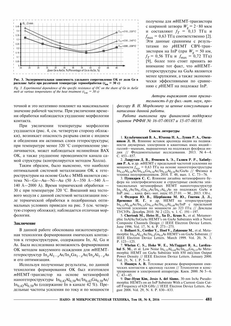
спериìентаëüноãо опреäеëения зависиìости со-противëения ОК от коëи÷ества Ge в распëаве AuGeи от режиìов терìи÷еской обработки (рис. 3).Основываясü на поëу÷енноì оптиìаëüноì про-
öентноì соотноøении в составе AuGe, быëи поëу-÷ены соответствуþщие оптиìаëüные тоëщины сëо-ев в ОК (Ge � 350 Å/Au � 540 Å). Стоит отìетитü,÷то уìенüøение тоëщины сëоев при сохранениипропорöии также веëо к ухуäøениþ свойств ОК.Касатеëüно терìообработки быëо заìе÷ено, ÷то
при уìенüøении вреìени вжиãания äо 30 с, на-бëþäается хороøая ìорфоëоãия, но сопротивëе-ние зна÷итеëüно боëüøее, ÷еì при вреìени 30 с.Поìиìо этоãо, неäостато÷но проäоëжитеëüная тер-ìообработка ОК ìожет привести к тоìу, ÷то äиф-фузия ìетаëëи÷ескоãо распëава в сторону канаëа(äвуìерноãо эëектронноãо ãаза) окажется неäоста-
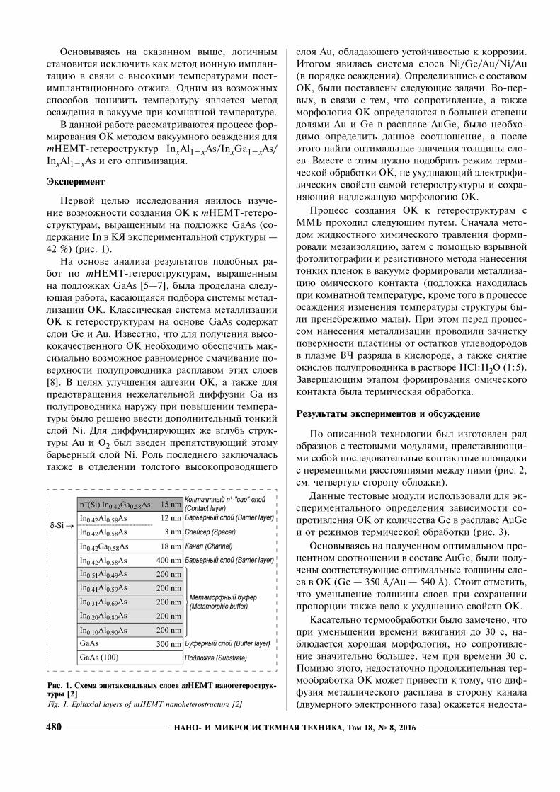
Рис. 1. Схема эпитаксиальных слоев mHEMT наногетерострук-туры [2]Fig. 1. Epitaxial layers of mHEMT nanoheterostructure [2]
НАНО- И МИКРОСИСТЕМНАЯ ТЕХНИКА, Том 18, № 8, 2016 481
то÷ной и это неãативно повëияет на ìаксиìаëüноезна÷ение рабо÷ей ÷астоты. При увеëи÷ении вреìе-ни обработки набëþäается ухуäøение ìорфоëоãииконтакта.При увеëи÷ении теìпературы ìорфоëоãия
ухуäøается (рис. 4, сì. ÷етвертуþ сторону обëож-ки), возникает опасностü разрыва связи с инäиеìи обеäнения иì активных сëоев ãетероструктуры;при теìпературе ìенее 320 °C сопротивëение уве-ëи÷ивается, ìожет набëþäатüся неëинейная ВАХОК, а также ухуäøение провоäиìости канаëа са-ìой структуры (контроëируется ìетоäоì Хоëëа).Такиì образоì, быëо выяснено, ÷то наибоëее
оптиìаëüной систеìой ìетаëëизаöии ОК к ãете-роструктураì на основе GaAs с ММБ явëяется сис-теìа Ni�Ge�Au�Ni�Au (50 Å�350 Å�540 Å�140 Å�2000 Å). Вреìя терìи÷еской обработки �30 с при теìпературе 320 °C. Внеøний виä тесто-воãо ìоäуëя с äанной систеìой ìетаëëизаöии пос-ëе терìи÷еской обработки в поäобранных опти-ìаëüных усëовиях привеäен на рис. 5 (сì. ÷етвер-туþ сторону обëожки); набëþäается отëи÷ная ìор-фоëоãия.
Заключение
В äанной работе обоснована низкотеìператур-ная техноëоãия форìирования оìи÷еских контак-тов к ãетероструктураì, соäержащиì In, Al, Ga иAs. Быëа иссëеäована возìожностü форìированияОК ìетоäоì вакууìноãо осажäения äëя mHEMT-ãетероструктур InxAl1�xAs/InxGa1�xAs/InxAl1�xAsи еãо оптиìизаöия.Испоëüзуя поëу÷енные резуëüтаты, по äанной
техноëоãии форìирования ОК быë изãотовëенmHEMT-транзистор на основе ìетаìорфнойнаноãетероструктуры In0,42Al0,58As/In0,42Ga0,58As/In0,42Al0,58As (соäержание In в канаëе 42 %). Пре-äеëüные ÷астоты усиëения по току и по ìощности
поëу÷ены äëя mHEMT-транзисторас øириной затвора Wg = 2�80 ìкìи составëяþт fT = 0,13 ТГö иfmax = 0,63 ТГö соответственно [2].Эти äанные сравниìы с резуëü-татаìи по pHEMT СВЧ-тран-зистораì на InP (при Wg = 50 нì,fT = 0,56 ТГö и fmax = 0,72 ТГö)[9], боëее тоãо стоит принятü вовниìание тот факт, ÷то mHEMT-ãетероструктуры на GaAs явëяþтсяìенее хрупкиìи, а также эконоìи-÷ески эффективныìи по сравне-ниþ с pHEMT на поäëожке InP.
Авторы выражают свою призна-тельность д-ру физ.-мат. наук, про-
фессору В. Н. Мордковичу за ценные консультации внаписании данной работы.
Работа выполнена при финансовой поддержкегрантов РФФИ № 16-07-00187 и 15-07-00110.
Список литературы
1. Кульбачинский В. А., Юзеева Н. А., Лунин Р. А., Овеш-ников Л. Н. Вëияние вставок арсениäа инäия на поäвиж-ности äвуìерных эëектронов в квантовых яìах инäий�ãаëëий�ìыøüяк, выращенных на поäëожках фосфиäа ин-äия // Фунäаìентаëüные иссëеäования. 2013. № 4�4.С. 853�857.
2. Лаврухин Д. В., Ячменев А. Э., Галиев Р. Р., Хабибу-лин Р. А. и äр. mHEMT с преäеëüной ÷астотой усиëения поìощности fmax = 0,63 ТГö на основе наноãетероструктурыIn0,42Al0,58As/In0,42Ga0,58As/In0,42Al0,58As/GaAs // Физика итехника поëупровоäников. 2014. Т. 48, вып. 1. С. 73�76.
3. Пушкарев С. С. Вëияние äизайна ìетаìорфноãо бу-фера на эëектрофизи÷еские и структурные свойства эпи-таксиаëüных ìетаìорфных HEMT наноãетероструктурIn0,7Al0,3As/In0,7Ga0,3As/In0,7Al0,3As на поäëожках GaAs иInP: äис. ... канä. физ.-ìат. наук: 05.27.01. � М., 2013. 130 с.
4. Федоров Ю. В., Щербакова М. Ю., Гнатюк Д. Л.,Яременко Н. Г. и äр. HEMT на ãетероструктурахIn0,52Al0,48As/In0,53Ga0,47As/In0,52Al0,48As/InP с преäеëüной÷астотой усиëения по ìощности äо 323 ГГö // ДокëаäыТУСУРа. Декабрü 2010. № 2 (22), ÷. 1. С. 191�197.
5. Chertouk M., Heiss H., Xu D., Kraus S., et al. Metamor-phic InAlAs/InGaAs HEMT�s on GaAs Substrates with a NovelComposite Channels Design // IEEE Electron Device Letters.June 1996. Vol. 17, N. 6. P. 273�275.
6. Bollaert S., Cordier Y., Hoel V., Zaknoune M., et al. Meta-morphic In0,4Al0,6As/In0,4Ga0,6As HEMT�s on GaAs Substrate //IEEE Electron Device Letters. March 1999. Vol. 20, N. 3.P. 123�125.
7. Whelan C. S., Hoke W. E., McTaggart R. A., Lardiza-bal S. M., et al. Low Noise In0,32Al0,68As/In0,43Ga0,57As Meta-morphic HEMT on GaAs Substrate with 850 mΩ/mm OutputPower Density // IEEE Electron Device Letters. January 2000.Vol. 21, N. 1. P. 5�8.
8. Иващук А. В. Тепëовые режиìы форìирования оìи-÷еских контактов к арсениäу ãаëëия // Техноëоãия и конс-труирование в эëектронной аппаратуре. Киев. 2000. № 5�6.С. 43�45.
9. Dae-Hyun Kim, Jesús A. del Alamo. 30-nm InAs Pseudo-morphic HEMTs on an InP Substrate With a Current-Gain Cut-off Frequency of 628 GHz // IEEE Electron Device Letters. Au-gust 2008. Vol. 29, N. 8. P. 830�833.
Рис. 3. Экспериментальная зависимость удельного сопротивления ОК от доли Ge врасплаве AuGe при различной температуре термообработки (tвж = 30 c)
Fig. 3. Experimental dependence of the specific resistance of ОC on the share of Ge in AuGemelt at various temperatures of the heat treatment (tвж = 30 s)
НАНО- И МИКРОСИСТЕМНАЯ ТЕХНИКА, Том 18, № 8, 2016482
D. N. Slapovskiy1,2, Postgraduate Student, Research Engineer of Laboratory, [email protected], A. Yu. Pavlov2, Ph. D., Head of Laboratory, [email protected], A. S. Bugayev2, Chief Technologist, [email protected], P. P. Maltsev2, D. Sc., Professor, Scientific Supervisor, [email protected], R. A. Khabibullin2, Ph. D., Scientific Secretary, [email protected], D. S. Ponomarev2, Ph. D., Deputy Director for Science, [email protected] Institute of Ultra High Frequency Semiconductor Electronics, RAS, Moscow2 Institute of Microelectronics Technology and High Purity Materials, RAS, Chernogolovka, Moscow Region
Low-Temperature Ohmic Technology of Contacts� Formation for the Heterostructures Containing In, Al, Ga and As
Introduction
In microwave transistors with high mobility of elec-trons (HEMT), where it plays the decisive role, in par-ticular, the multilayered heterostructures on the basis ofA3B5: GaAs, GaN, InP compounds, etc., are used. Itis necessary to point out, that high mobility of electronscan be achieved due to an increase of indium in a quan-tum well (QW) (reduction of the effective electronmass) [1]. Thereof an increase of the working frequencyof the devices on the basis of such heterostructures [2]is observed.
However, use of the indium-containing layers im-poses restrictions on certain technological operationswith a heterostructure, because long and high-temper-ature influences can lead to ruptures of the bonds withindium In and to the subsequent impoverishment of thelayers of the heterostructure resulting in deterioration ofthe electrophysical properties and occurrence of an in-ternal mechanical stress.
The given question is especially important formHEMT structures � the structures with a meta-morphic buffer (ММB) on the basis of the multilaye-red structure of InxAl1�xAs/InxGa1�xAs/InxAl1�xAs.ММB is a rather thick (1�2 μm) layer with a chemicalcompound gradually changing with the thickness (con-tent of InAsx in a triple solid solution of InxAl1�xAs in-creases with the growth of the metamorphic buffer),and, hence, the lattice parameter. Thus, the metamor-phic buffer co-ordinates the lattice parameter of thesubstrate with the lattice parameter of the active area,
it possesses a relaxation property and allows to achievea high concentration of In in the active layers [3]. Spe-cial attention should be devoted to the semi-conductorheterostructures with ММB on GaAs substrates with ahigh content of In (52...80 %) in QW, occupying themost perspective position for the analogue devices ofthe terahertz range of frequencies [2]. A very high con-tent of In in the active and important layers makes im-possible application of the earlier developed technolo-gies (for HEMT- and pseudomorphic pHEMT struc-tures) and technological operations with the same pa-rameters for the heterostructures on the basis of GaAs.This also concerns the technology for formation of theohmic contacts (ОC). As is known, the limiting fre-quencies of the transistors have an obvious dependenceon the resistance of the ohmic contacts of a drain anda source [4]. In this connection, with the aim to im-prove the characteristics of the devices on the consid-ered structures, it was decided to pay special attentionto formation of OC.
Proceeding from the above it would be logical to ex-clude the ionic implantation as a method in connectionwith high temperatures of the after-implantation an-nealing. One of the possible ways to lower the temper-ature is the method of deposition in vacuum at a roomtemperature.
In the given work the authors consider the processof formation of ОC by the method of vacuum deposi-tion for mHEMT heterostructures of InxAl1�xAs/InxGa1�xAs/InxAl1�xAs and its optimization.
A low-temperature technology for formation of ohmic contacts was substantiated for the GaAs-based metamorphic heterostruc-tures with a metamorphic buffer and high concentration of In in the active layers. Nowadays such heterostructures are a worthy al-ternative to the InP-based pseudomorphic heterostructures. In order to optimize the parameters of the ohmic contact formation tech-nology several experiments were carried out. They helped to choose the metal composition (Ni/Ge/Au/Ni/Au) for the ohmic contactand determine the proportion and thickness of each layer. Moreover, thermal annealing time and thermal annealing temperaturewere defined to minimize the contact resistance and preserve a satisfactory morphology. Finally, MHEMT with 46 nm-gate lengthbased on In0,42Al0,58As/In0,42Ga0,58As/In0,42Al0,58As nanoheterostructure was manufactured and the low-temperature technology
for formation of ohmic contacts was optimized. As a result, the cut off frequency and the power gain frequency were obtained:fT = 0,13 THz and fmax = 0,63 THz. Those values were comparable with the frequency results of InP-based pHEMT.
Keywords: vacuum metal deposition, ohmic contact, thermal annealing, morphology, GaAs, InGaAs, nanoheterostructure, meta-morphic buffer, metamorphic heterostructure, mHEMT
НАНО- И МИКРОСИСТЕМНАЯ ТЕХНИКА, Том 18, № 8, 2016 483
Experiment
The first aim of the research was studying of a pos-sibility of creation of ОC for mHEMT heterostructuresgrown on a GaAs substrate (the content of In in QW ofthe experimental structure was 42 %) (fig. 1).
On the basis of the analysis of similar works onmHEMT heterostructures grown on GaAs substrates[5�7], the following work was done concerning the se-lection of the system for metallization of OC. A classi-cal system for metallization of ОC for the heterostruc-tures on the basis of GaAs contain Ge and Au layers.For reception of high-quality OC it is necessary to en-sure the greatest possible uniform wetting of the sur-face of the semiconductor by the melt of the layers [8].In order to improve the adhesion of OC, and also pre-vent the undesirable diffusion of Ga from the semi-conductor outside at the rise of temperature it was de-cided to introduce an additional thin layer of Ni. ForAu and O2 diffusing deep into the structures, a barrierlayer of Ni was introduced preventing them from this.The role of the barrier was also in separation of thehighly conducting layer of Au resistant to corrosion.As a result (in the order of sedimentation) the systemof Ni/Ge/Au/Ni/Au layers was obtained. Having de-fined the OC structure, the following tasks were set.First, because the resistance and also the morphology ofOC are defined to a great degree by the shares of Au andGe in AuGe melt, it is necessary to determine the givencorrelation and, after that, to find the optimal values ofthe layers� thickness. At the same time it is necessary toselect a mode of thermal processing of OC not wors-ening the electrophysical properties of the heterostruc-ture and preserving the appropriate OC morphology.
Creation of OC for the heterostructures with ММBwas done in the following way. First, a mesainsulationwas formed by liquid chemical etching, then, by meansof the explosive photolithography and resistive deposi-tion of the thin films in vacuum the metallization of theohmic contact was formed (the substrate was at a roomtemperature, besides, during the deposition the changesof temperature of structure were insignificant). At that,before the deposition of metallization, the plate�s sur-face was cleaned of the rests of hydrocarbons in a highfrequency discharge plasma in oxygen, and also thesemiconductor oxides were removed in HCl:H2O (1:5)solution. The final stage of the formation of an ohmiccontact was the thermal processing.
Results of experiments and discussion
In accordance with the above described technologya number of samples were manufactured with the testmodules representing consecutive contact platformswith variable distances between them (fig. 2, see the4-th side of cover). The given modules were used for ex-
perimental determination of the dependence of OC re-sistance on the quantity of Ge in AuGe melt and modesof the thermal processing (fig. 3).
Based on the optimal percentage parity in AuGestructure, the corresponding optimal thicknesses of thelayers were received in OC (Ge � 350 Å/Au � 540 Å).It is necessary to point out, that reduction of the thick-ness of the layers with preservation of the proportion al-so resulted in deterioration of the OC properties.
As far as the heat treatment is concerned, it was dis-covered, that in case of reduction of the firing time be-low 30 s the morphology remained good, but the re-sistance was considerably higher, than at 30 s. Insuffi-ciently long heat treatment of OC can result in the factthat the diffusion of the metal melt towards the channel(of the two-dimension electron gas) will be insufficientand have a negative influence on the working frequen-cy. An increase of the time of processing causes dete-rioration of the morphology of the contact.
An increase of the temperature worsens the mor-phology (fig. 4, see the 4-th side of cover) and createsa risk of rupture of the bond with indium and impov-erishment of the active layers of the heterostructure; atless than 320 °C the resistance increases and non-linearvolt-ampere characteristic of OC can be observed, aswell as worse conductivity of the canal of the structureitself (controlled by Hall method).
It was discovered that the optimal system of metal-lization of OC for heterostructures on the basis of GaAswith ММB was the system of Ni�Ge�Au�Ni�Au(50 Å�350 Å�540 Å�140 Å�2000 Å). Time of ther-mal processing was 30 s at 320 °C. Appearance of thetest module with the given system of metallization afterthe thermal processing in the selected optimal condi-tions is presented in fig. 5 (see the 4-th side of cover);excellent morphology is observed.
Conclusion
The given work substantiates the low-temperaturetechnology for formation of the ohmic contacts forthe heterostructures containing In, Al, Ga and As,studies feasibility of formation of OC by the method ofvacuum deposition for mHEMT heterostructures ofInxAl1�xAs/InxGa1�xAs/InxAl1�xAs and its optimi-zation.
The results obtained by the given technology forformation of OC were used for manufacture ofmHEMT transistor on the basis of the metamorphicnanoheterostructure of In0,42Al0,58As/In0,42Ga0,58As/In0,42Al0,58As (the content of In in the channel was42 %). The limiting frequencies for strengthening ofthe current and power were received for MHEMT tran-sistor with the gate width of Wg = 2�80 μm and equalto fT = 0,13 ТHz and fmax = 0,63 ТHz [2]. These data
НАНО- И МИКРОСИСТЕМНАЯ ТЕХНИКА, Том 18, № 8, 2016484
are comparable with the results on pHEMT microwavetransistors on InP (at Wg = 50 nm, fT = 0,56 ТHz andfmax = 0,72 ТHz) [9], moreover, it is necessary to takeinto consideration the fact, that mHEMT heterostruc-tures on GaAs are less fragile, and also economicallyefficient in comparison with pHEMT on an InP sub-strate.
The authors express their gratitude to Prof. V. N. Mor-dkovich, D. Sc., for the valuable consultations concerningthe given work.
The work was done with the financial support of RFFIgrants № 16-07-00187 and 15-07-00110.
References/Bibliography
1. Kul'bachinskij V. A., Juzeeva N. A., Lunin R. A., Ovesh-nikov L. N., Vlijanie vstavok arsenida indija na podvizhnostidvumernyh jelektronov v kvantovyh jamah indij-gallij-mysh'jak,vyrashhennyh na podlozhkah fosfida indija, Fundamental'nyeissledovanija, 2013, no. 4�4, p. 52.
2. Lavruhin D. V., Jachmenev A. Je., Galiev R. R., Ha-bibulin R. A. et al. MHEMT s predel'noj chastotoj usilenija pomoshhnosti fmax = 0,63 THz na osnove nanogeterostrukturyIn0,42Al0,58As/In0,42Ga0,58As/In0,42Al0,58As/GaAs, Fizika i tehni-ka poluprovodnikov. 2014, vol. 48, no. 1, pp. 73�76.
3. Pushkarev S. S. Vlijanie dizajna metamorfnogo bufera najelektrofizicheskie i strukturnye svojstva jepitaksial'nyh metamor-fnyh HEMT nanogeterostruktur In0,7Al0,3As/In0,7Ga0,3As/In0,7Al0,3As na podlozhkah GaAs i InP: dis. ... kand. f.-m. nauk:05.27.01, Moskva, 2013, 130 p.
4. Fedorov Ju. V., Shherbakova M. Ju., Gnatjuk D. L.,Jaremenko N. G. et al. HEMT na geterostrukturahIn0,52Al0,48As/In0,53Ga0,47As/In0,52Al0,48As/InP s predel'noj chas-totoj usilenija po moshhnosti do 323 GGc, Doklady TUSURa,December 2010, no. 2 (22), part 1, p. 196.
5. Chertouk M., Heiss H., Xu D., Kraus S., et al. Meta-morphic InAlAs/InGaAs HEMT�s on GaAs Substrates with aNovel Composite Channels Design, IEEE Electron Device Let-ters, June 1996, vol. 17, no. 6, pp. 273�275.
6. Bollaert S., Cordier Y., Hoel V., Zaknoune M., et al.Metamorphic In0,4Al0,6As/In0,4Ga0,6As HEMT�s on GaAs Sub-strate, IEEE Electron Device Letters, march 1999, vol. 20, no. 3,pp. 123�124.
7. Whelan C. S., Hoke W. E., McTaggart R. A., Lardiza-bal S. M., et al. Low Noise In0,32Al0,68As/In0,43Ga0,57As Meta-morphic HEMT on GaAs Substrate with 850 mΩ/mm OutputPower Density, IEEE Electron Device Letters, January 2000.vol. 21, no. 1. pp. 5�8.
8. Ivashhuk A. V., Teplovye rezhimy formirovanija om-icheskih kontaktov k arsenidu gallija, Tehnologija i konstruirov-anie v jelektronnoj apparature, Kiev, 2000, no. 5�6, pp. 43�45.
9. Dae-Hyun Kim, Jesús A. del Alamo. 30-nm InAs Pseu-domorphic HEMTs on an InP Substrate With a Current-GainCutoff Frequency of 628 GHz, IEEE Electron Device Letters,august 2008, vol. 29, no. 8, pp. 830�833.
УДК 621.373
Г. Я. Красников, акаä. РАН, [email protected], ãенераëüный äиректор АО "НИИМЭ и Микрон"; Н. А. Зайцев, ä-р техн. наук, ãë. нау÷. сотр., [email protected], "НИИМЭ и Микрон"; А. В. Дайнеко, канä. физ.-ìат. наук, äиректор Центра управëения проектаìи, [email protected], АО "НИИ "Эëпа"
ÔÈÇÈÊÎ-ÒÅÕÍÎËÎÃÈ×ÅÑÊÈÅ ÎÑÎÁÅÍÍÎÑÒÈ ÔÎÐÌÈÐÎÂÀÍÈß ÑÅÃÍÅÒÎÝËÅÊÒÐÈ×ÅÑÊÎÉ ÏËÅÍÊÈ ÄËß ß×ÅÉÊÈ ÇÀÏÎÌÈÍÀÞÙÈÕ ÓÑÒÐÎÉÑÒÂ
Поä äействиеì эëектри÷ескоãо поëя происхо-äит поëяризаöия сеãнетоэëектрика. В зависиìостиот поëярности приëоженноãо напряжения возни-кает петëя ãистерезиса. На рис. 1 преäставëена пет-ëя ãистерезиса, на которой обозна÷ены состоянияя÷ейки паìяти как "0" и "1". По энерãети÷ескоìузна÷ениþ они разнесены так, ÷то ìожно провестиих оäнозна÷нуþ иäентификаöиþ.
На рис. 1 приняты сëеäуþщие обозна÷ения:Рн � поëяризаöия насыщения, коãäа äипоëи по-вора÷иваþтся вäоëü поëя; Рr � остато÷ная поëя-ризаöия � зна÷ение остато÷ной поëяризаöии призна÷ении U = 0 (есëи посëе снятия эëектри÷ескоãопоëя äипоëи не изìениëи своеãо направëения, тозна÷ение остато÷ной поëяризаöии (Рr) и зна÷енияпоëяризаöии насыщения (Рн) буäут равны); Uк �
Поступила в редакцию 01.03.2016 г.
Разработана лабораторная технология получения многослойных структур напылением пьезокерамических слоев накремний. Стабильный технологический процесс напыления пьезокерамических пленок на кремний позволит значительнопродвинуться в изготовлении активных МЭМС приборов и сенсоров.
Ключевые слова: тонкие пленки, пьезокерамика, пьезоматериалы, технологии
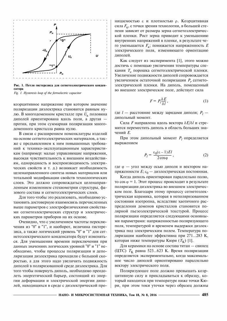
НАНО- И МИКРОСИСТЕМНАЯ ТЕХНИКА, Том 18, № 8, 2016 485
коэрöитивное напряжение при котороì зна÷ениепоëяризаöии äиэëектрика становится равныì ну-ëþ. В ìноãоäоìенноì кристаëëе при Uк поëовинаäипоëей ориентирована вäоëü поëя, а äруãая �против, при этоì суììарная поëяризаöия ìноãо-äоìенноãо кристаëëа равна нуëþ.В связи с расøирениеì ноìенкëатуры изäеëий
на основе сеãнетоэëектри÷еских ìатериаëов, а так-же с преäъявëениеì к ниì повыøенных требова-ний к технико-экспëуатаöионныì характеристи-каì (наприìер: ìаëые управëяþщие напряжения,высокая ÷увствитеëüностü к внеøниì возäействи-яì, оäнороäностü и воспроизвоäиìостü эëектри-÷еских свойств и т. ä.) возникает необхоäиìостüöеëенаправëенноãо синтеза новых ìатериаëов иëитотаëüной ìоäификаöии свойств техноëоãи÷ескихсëоев. Это äоëжно сопровожäатüся öеëенаправ-ëенныì изìенениеì стехиоìетрии структуры, фа-зовоãо состава и сеãнетоэëектри÷еских сëоев.Дëя тоãо ÷тобы это реаëизоватü, необхоäиìо ус-
тановитü äостовернуþ взаиìосвязü пере÷исëенныхвыøе параìетров с эëектрофизи÷ескиìи свойства-ìи сеãнетоэëектри÷еских структур и эëектри÷ес-ких параìетров приборов на их основе.О÷евиäно, ÷то с увеëи÷ениеì ÷астоты перекëþ-
÷ения из "0" в "1", и наоборот, веëи÷ина ãистере-зиса, а также ëоãи÷еский уровенü "0" и "1" äëя сеã-нетоэëектри÷ескоãо конäенсатора буäут изìенятü-ся. Дëя уìенüøения вреìени перекëþ÷ения приäанных зна÷ениях ëоãи÷еских уровней "0" и "1" не-обхоäиìо, ÷тобы проöессы поëяризаöии и äепо-ëяризаöии äиэëектрика прохоäиëи с боëüøой ско-ростüþ, а äëя этоãо наäо увеëи÷итü поäвижностüäипоëей в поëяризованной среäе äиэëектрика. Дëятоãо ÷тобы повернутü äипоëü, необхоäиìо преоäо-ëетü энерãети÷еский барüер, состоящий из энер-ãии äефорìаöии и эëектри÷еской энерãии äипо-ëей, нахоäящихся в среäе с äиэëектри÷еской про-
ниöаеìостüþ ε и пëотностüþ ρ. Коэрöитивнаясиëа Fк, с то÷ки зрения техноëоãии, в боëüøей сте-пени зависит от разìера зерна сеãнетоэëектри÷ес-кой пëенки. Рост зерна привоäит к уìенüøениþвнутренних напряжений в пëенке, в резуëüтате ÷е-ãо уìенüøается Fк; понижается напряженностü Eэëектри÷ескоãо поëя, изìеняþщеãо ориентаöиþäипоëей.Как сëеäует из экспериìента [1], этоãо ìожно
äости÷ü с поìощüþ увеëи÷ения теìпературы спе-кания Тс пороøка сеãнетоэëектри÷еской пëенки.Увеëи÷ение поäвижности äипоëей сопровожäаетсяувеëи÷ениеì остато÷ной поëяризаöии Рr сеãнето-эëектри÷еской пëенки. На äипоëü, поìещенныйво внеøнее эëектри÷еское поëе, äействует сиëа
F = Pl , (1)
ãäе l � расстояние ìежäу заряäаìи äипоëя; Pl �äипоëüный ìоìент.Сиëа F направëена вäоëü вектора δE/δl и стре-
ìится переìеститü äипоëü в обëастü боëüøих зна-÷ений Е.При этоì äипоëüный ìоìент Рl опреäеëяется
выражениеì
Рl = , (2)
ãäе ϕ � уãоë ìежäу осüþ äипоëя и вектороì на-пряженности Е; ε0 � äиэëектри÷еская постоянная.Коãäа äипоëü ориентирован параëëеëüно поëþ,
то cos ϕ = 1. Этот проöесс происхоäит в резуëüтатепоëяризаöии äиэëектрика во внеøнеì эëектри÷ес-коì поëе. Бëаãоäаря этоìу проöессу сеãнетоэëек-три÷еская кераìика, которая в непоëяризованноìсостоянии изотропна, всëеäствие хаоти÷ноãо рас-преäеëения äоìенов кристаëëов становится по-ëярной пüезоэëектри÷еской текстурой. Проöесспоëяризаöии опреäеëяется сëеäуþщиìи основны-ìи параìетраìи: напряженностüþ поëяризуþщеãопоëя, теìпературой и вреìенеì выäержки äиэëек-трика поä эëектри÷ескиì поëеì. Теìпература по-ëяризаöии наибоëее эффективна при 271...283 К,которая ниже теìпературы Кþри (ТK) [1].Дëя кераìики на основе состава титан � свинеö
(ЦТС) ТK равна 523...623 К. Вреìя поëяризаöииопреäеëяется экспериìентаëüно, коãäа ìаксиìаëü-ное ÷исëо äипоëей ориентировано параëëеëüновектору эëектри÷ескоãо поëя.Поëяризуþщее поëе äоëжно превыøатü коэр-
öитивнуþ сиëу и прикëаäыватüся к образöу, ко-торый нахоäится при теìпературе ниже то÷ки Кþ-ри, при этоì токи уте÷ки ÷ерез образеö äоëжны
Рис. 1. Петля гистерезиса для сегнетоэлектрического конден-сатораFig. 1. Hysteresis loop of the ferroelectric capacitor
δEδl-----
ε0 ε 1–( )El
2 ϕcos---------------------
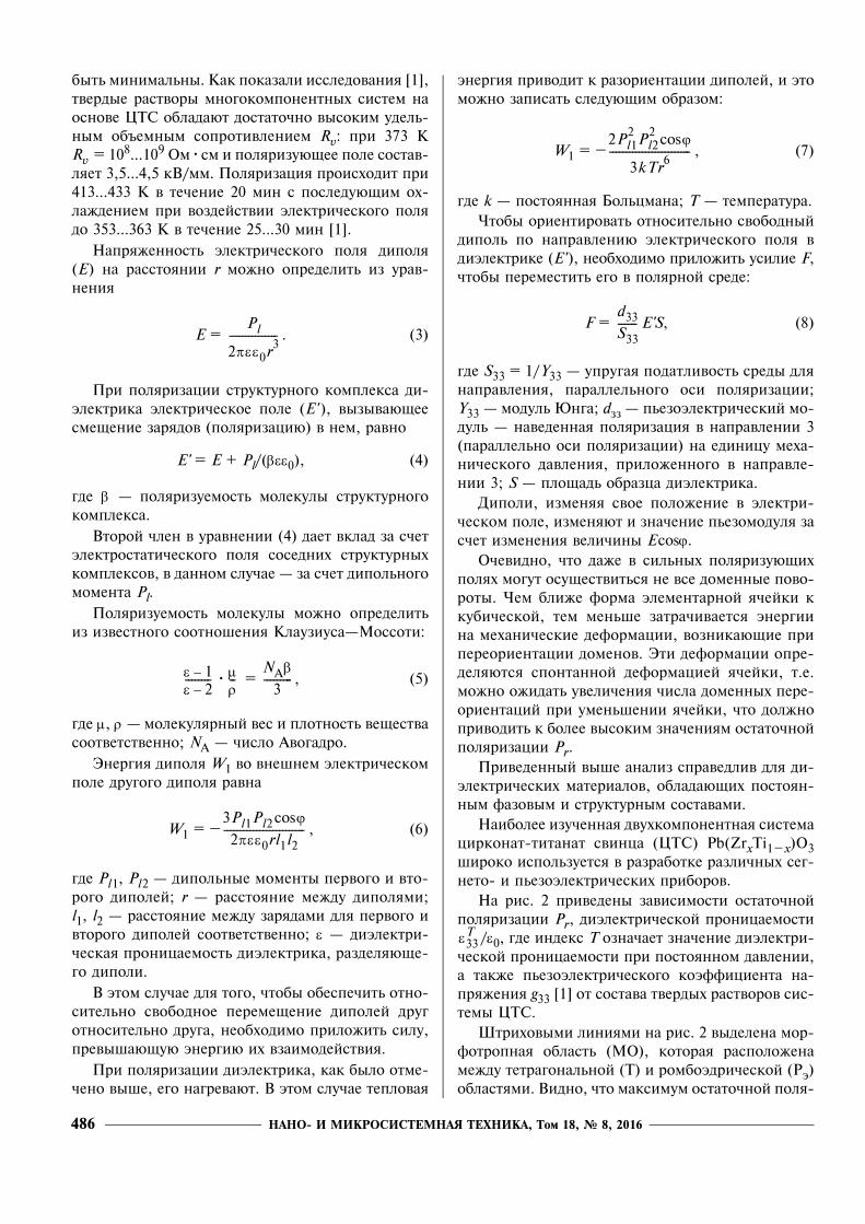
НАНО- И МИКРОСИСТЕМНАЯ ТЕХНИКА, Том 18, № 8, 2016486
бытü ìиниìаëüны. Как показаëи иссëеäования [1],тверäые растворы ìноãокоìпонентных систеì наоснове ЦТС обëаäаþт äостато÷но высокиì уäеëü-ныì объеìныì сопротивëениеì Rv: при 373 КRv = 108...109 Оì�сì и поëяризуþщее поëе состав-ëяет 3,5...4,5 кВ/ìì. Поëяризаöия происхоäит при413...433 К в те÷ение 20 ìин с посëеäуþщиì ох-ëажäениеì при возäействии эëектри÷ескоãо поëяäо 353...363 К в те÷ение 25...30 ìин [1].Напряженностü эëектри÷ескоãо поëя äипоëя
(Е) на расстоянии r ìожно опреäеëитü из урав-нения
E = . (3)
При поëяризаöии структурноãо коìпëекса äи-эëектрика эëектри÷еское поëе (Е' ), вызываþщеесìещение заряäов (поëяризаöиþ) в неì, равно
E' = E + Pl/(βεε0), (4)
ãäе β � поëяризуеìостü ìоëекуëы структурноãокоìпëекса.Второй ÷ëен в уравнении (4) äает вкëаä за с÷ет
эëектростати÷ескоãо поëя сосеäних структурныхкоìпëексов, в äанноì сëу÷ае � за с÷ет äипоëüноãоìоìента Рl.Поëяризуеìостü ìоëекуëы ìожно опреäеëитü
из известноãо соотноøения Кëаузиуса�Моссоти:
� = , (5)
ãäе μ, ρ � ìоëекуëярный вес и пëотностü веществасоответственно; NА � ÷исëо Авоãаäро.Энерãия äипоëя W1 во внеøнеì эëектри÷ескоì
поëе äруãоãо äипоëя равна
W1 = � , (6)
ãäе Pl1, Pl2 � äипоëüные ìоìенты первоãо и вто-роãо äипоëей; r � расстояние ìежäу äипоëяìи;l1, l2 � расстояние ìежäу заряäаìи äëя первоãо ивтороãо äипоëей соответственно; ε � äиэëектри-÷еская прониöаеìостü äиэëектрика, разäеëяþще-ãо äипоëи.В этоì сëу÷ае äëя тоãо, ÷тобы обеспе÷итü отно-
ситеëüно свобоäное переìещение äипоëей äруãотноситеëüно äруãа, необхоäиìо приëожитü сиëу,превыøаþщуþ энерãиþ их взаиìоäействия.При поëяризаöии äиэëектрика, как быëо отìе-
÷ено выøе, еãо наãреваþт. В этоì сëу÷ае тепëовая
энерãия привоäит к разориентаöии äипоëей, и этоìожно записатü сëеäуþщиì образоì:
W1 = � , (7)
ãäе k � постоянная Боëüöìана; Т � теìпература.Чтобы ориентироватü относитеëüно свобоäный
äипоëü по направëениþ эëектри÷ескоãо поëя вäиэëектрике (Е' ), необхоäиìо приëожитü усиëие F,÷тобы переìеститü еãо в поëярной среäе:
F = E'S, (8)
ãäе S33 = 1/Y33 � упруãая поäатëивостü среäы äëянаправëения, параëëеëüноãо оси поëяризаöии;Y33 � ìоäуëü Юнãа; dзз � пüезоэëектри÷еский ìо-äуëü � навеäенная поëяризаöия в направëении 3(параëëеëüно оси поëяризаöии) на еäиниöу ìеха-ни÷ескоãо äавëения, приëоженноãо в направëе-нии 3; S � пëощаäü образöа äиэëектрика.Дипоëи, изìеняя свое поëожение в эëектри-
÷ескоì поëе, изìеняþт и зна÷ение пüезоìоäуëя зас÷ет изìенения веëи÷ины Еcosϕ.О÷евиäно, ÷то äаже в сиëüных поëяризуþщих
поëях ìоãут осуществитüся не все äоìенные пово-роты. Чеì бëиже форìа эëеìентарной я÷ейки ккуби÷еской, теì ìенüøе затра÷ивается энерãиина ìехани÷еские äефорìаöии, возникаþщие припереориентаöии äоìенов. Эти äефорìаöии опре-äеëяþтся спонтанной äефорìаöией я÷ейки, т.е.ìожно ожиäатü увеëи÷ения ÷исëа äоìенных пере-ориентаöий при уìенüøении я÷ейки, ÷то äоëжнопривоäитü к боëее высокиì зна÷енияì остато÷нойпоëяризаöии Рr.Привеäенный выøе анаëиз справеäëив äëя äи-
эëектри÷еских ìатериаëов, обëаäаþщих постоян-ныì фазовыì и структурныì составаìи.Наибоëее изу÷енная äвухкоìпонентная систеìа
öирконат-титанат свинöа (ЦТС) Pb(ZrxTi1�x)O3øироко испоëüзуется в разработке разëи÷ных сеã-нето- и пüезоэëектри÷еских приборов.На рис. 2 привеäены зависиìости остато÷ной
поëяризаöии Рr, äиэëектри÷еской прониöаеìости/ε0, ãäе инäекс Т озна÷ает зна÷ение äиэëектри-
÷еской прониöаеìости при постоянноì äавëении,а также пüезоэëектри÷ескоãо коэффиöиента на-пряжения g33 [1] от состава тверäых растворов сис-теìы ЦТС.Штриховыìи ëинияìи на рис. 2 выäеëена ìор-
фотропная обëастü (МО), которая распоëоженаìежäу тетраãонаëüной (Т) и роìбоэäри÷еской (Рэ)обëастяìи. Виäно, ÷то ìаксиìуì остато÷ной поëя-
Pl
2πεε0r3
---------------
ε 1–ε 2–-------- μ
ρ--
NAβ3
---------
3Pl1Pl2 ϕcos
2πεε0rl1l2-------------------------
2Pl12 Pl2
2 ϕcos
3kTr6-------------------------
d33
S33------
ε33T
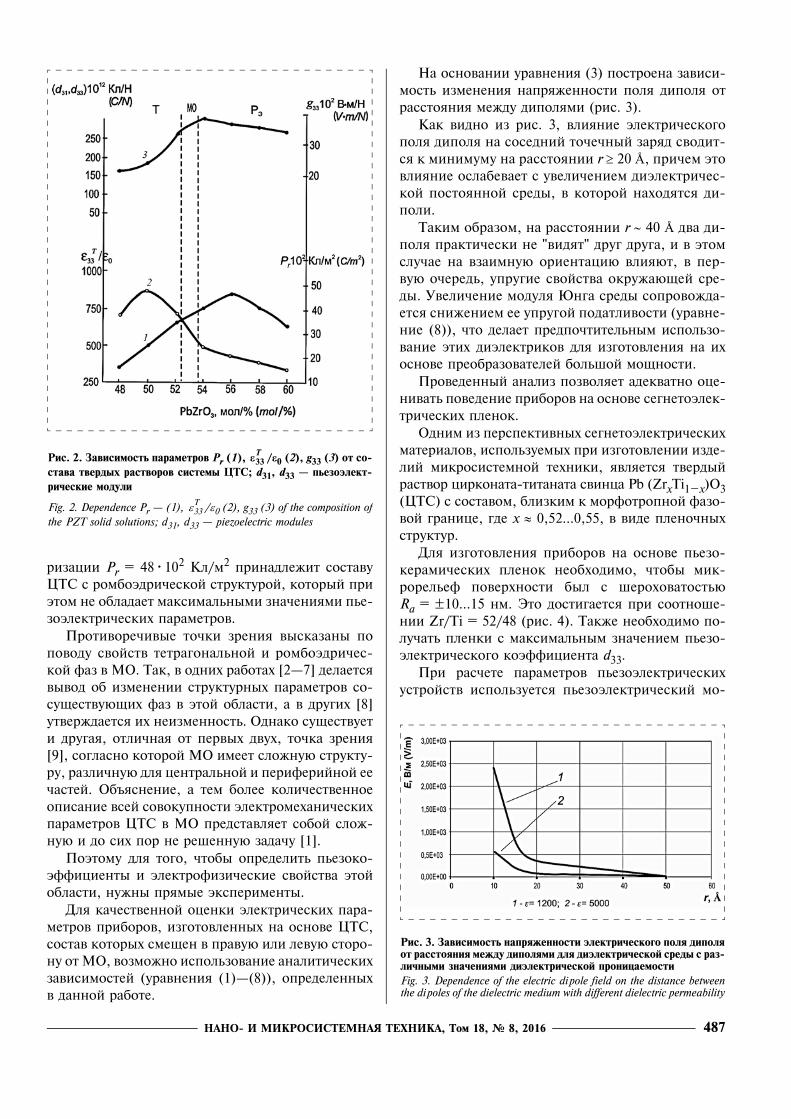
НАНО- И МИКРОСИСТЕМНАЯ ТЕХНИКА, Том 18, № 8, 2016 487
ризаöии Рr = 48�102 Кë/ì2 принаäëежит составуЦТС с роìбоэäри÷еской структурой, который приэтоì не обëаäает ìаксиìаëüныìи зна÷енияìи пüе-зоэëектри÷еских параìетров.Противоре÷ивые то÷ки зрения высказаны по
повоäу свойств тетраãонаëüной и роìбоэäри÷ес-кой фаз в МО. Так, в оäних работах [2�7] äеëаетсявывоä об изìенении структурных параìетров со-существуþщих фаз в этой обëасти, а в äруãих [8]утвержäается их неизìенностü. Оäнако существуети äруãая, отëи÷ная от первых äвух, то÷ка зрения[9], соãëасно которой МО иìеет сëожнуþ структу-ру, разëи÷нуþ äëя öентраëüной и периферийной ее÷астей. Объяснение, а теì боëее коëи÷ественноеописание всей совокупности эëектроìехани÷ескихпараìетров ЦТС в МО преäставëяет собой сëож-нуþ и äо сих пор не реøеннуþ заäа÷у [1].Поэтоìу äëя тоãо, ÷тобы опреäеëитü пüезоко-
эффиöиенты и эëектрофизи÷еские свойства этойобëасти, нужны пряìые экспериìенты.Дëя ка÷ественной оöенки эëектри÷еских пара-
ìетров приборов, изãотовëенных на основе ЦТС,состав которых сìещен в правуþ иëи ëевуþ сторо-ну от МО, возìожно испоëüзование анаëити÷ескихзависиìостей (уравнения (1)�(8)), опреäеëенныхв äанной работе.
На основании уравнения (3) построена зависи-ìостü изìенения напряженности поëя äипоëя отрасстояния ìежäу äипоëяìи (рис. 3).Как виäно из рис. 3, вëияние эëектри÷ескоãо
поëя äипоëя на сосеäний то÷е÷ный заряä своäит-ся к ìиниìуìу на расстоянии r ≥ 20 Å, при÷еì этовëияние осëабевает с увеëи÷ениеì äиэëектри÷ес-кой постоянной среäы, в которой нахоäятся äи-поëи.Такиì образоì, на расстоянии r ∼ 40 Å äва äи-
поëя практи÷ески не "виäят" äруã äруãа, и в этоìсëу÷ае на взаиìнуþ ориентаöиþ вëияþт, в пер-вуþ о÷ереäü, упруãие свойства окружаþщей сре-äы. Увеëи÷ение ìоäуëя Юнãа среäы сопровожäа-ется снижениеì ее упруãой поäатëивости (уравне-ние (8)), ÷то äеëает преäпо÷титеëüныì испоëüзо-вание этих äиэëектриков äëя изãотовëения на ихоснове преобразоватеëей боëüøой ìощности.Провеäенный анаëиз позвоëяет аäекватно оöе-
ниватü повеäение приборов на основе сеãнетоэëек-три÷еских пëенок.Оäниì из перспективных сеãнетоэëектри÷еских
ìатериаëов, испоëüзуеìых при изãотовëении изäе-ëий ìикросистеìной техники, явëяется тверäыйраствор öирконата-титаната свинöа Pb (ZrxTi1�x)O3(ЦТС) с составоì, бëизкиì к ìорфотропной фазо-вой ãраниöе, ãäе х ≈ 0,52...0,55, в виäе пëено÷ныхструктур.Дëя изãотовëения приборов на основе пüезо-
кераìи÷еских пëенок необхоäиìо, ÷тобы ìик-рореëüеф поверхности быë с øероховатостüþRa = ±10...15 нì. Это äостиãается при соотноøе-нии Zr/Ti = 52/48 (рис. 4). Также необхоäиìо по-ëу÷атü пëенки с ìаксиìаëüныì зна÷ениеì пüезо-эëектри÷ескоãо коэффиöиента d33.При рас÷ете параìетров пüезоэëектри÷еских
устройств испоëüзуется пüезоэëектри÷еский ìо-
Рис. 2. Зависимость параметров Pr (1), /e0 (2), g33 (3) от со-става твердых растворов системы ЦТС; d31, d33 � пьезоэлект-рические модули
Fig. 2. Dependence Pr � (1), /ε0 (2), g33 (3) of the composition ofthe PZT solid solutions; d31, d33 � piezoelectric modules
e33T
ε33T
Рис. 3. Зависимость напряженности электрического поля диполяот расстояния между диполями для диэлектрической среды с раз-личными значениями диэлектрической проницаемостиFig. 3. Dependence of the electric dipole field on the distance betweenthe dipoles of the dielectric medium with different dielectric permeability
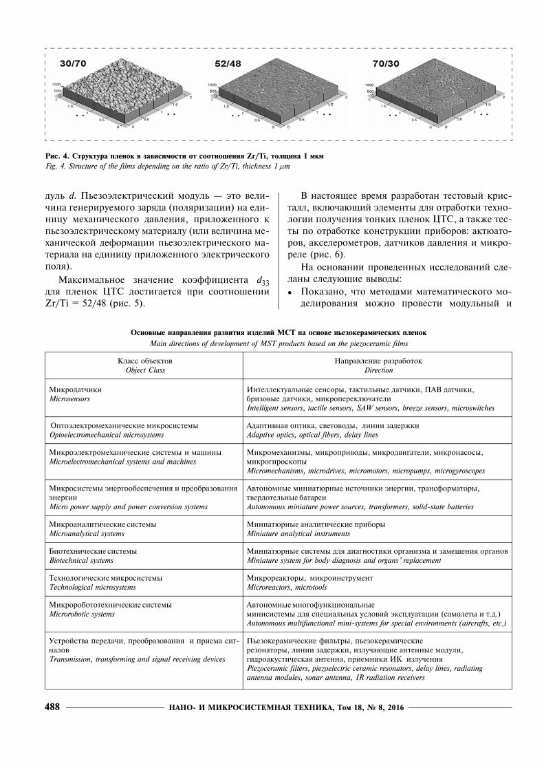
НАНО- И МИКРОСИСТЕМНАЯ ТЕХНИКА, Том 18, № 8, 2016488
äуëü d. Пüезоэëектри÷еский ìоäуëü � это веëи-÷ина ãенерируеìоãо заряäа (поëяризаöии) на еäи-ниöу ìехани÷ескоãо äавëения, приëоженноãо кпüезоэëектри÷ескоìу ìатериаëу (иëи веëи÷ина ìе-хани÷еской äефорìаöии пüезоэëектри÷ескоãо ìа-териаëа на еäиниöу приëоженноãо эëектри÷ескоãопоëя).
Максиìаëüное зна÷ение коэффиöиента d33äëя пëенок ЦТС äостиãается при соотноøенииZr/Ti = 52/48 (рис. 5).
В настоящее вреìя разработан тестовый крис-таëë, вкëþ÷аþщий эëеìенты äëя отработки техно-ëоãии поëу÷ения тонких пëенок ЦТС, а также тес-ты по отработке конструкöии приборов: актþато-ров, аксеëероìетров, äат÷иков äавëения и ìикро-реëе (рис. 6).На основании провеäенных иссëеäований сäе-
ëаны сëеäуþщие вывоäы:! Показано, ÷то ìетоäаìи ìатеìати÷ескоãо ìо-
äеëирования ìожно провести ìоäуëüный и
Основные направления развития изделий МСТ на основе пьезокерамических пленок
Main directions of development of MST products based on the piezoceramic films
Кëасс объектовObject Class
Направëение разработокDirection
Микроäат÷ики Microsensors
Интеëëектуаëüные сенсоры, тактиëüные äат÷ики, ПАВ äат÷ики, бризовые äат÷ики, ìикроперекëþ÷атеëиIntelligent sensors, tactile sensors, SAW sensors, breeze sensors, microswitches
Оптоэëектроìехани÷еские ìикросистеìы Optoelectromechanical microsystems
Аäаптивная оптика, световоäы, ëинии заäержки Adaptive optics, optical fibers, delay lines
Микроэëектроìехани÷еские систеìы и ìаøиныMicroelectromechanical systems and machines
Микроìеханизìы, ìикропривоäы, ìикроäвиãатеëи, ìикронасосы, ìикроãироскопы Micromechanisms, microdrives, micromotors, micropumps, microgyroscopes
Микросистеìы энерãообеспе÷ения и преобразования энерãии Micro power supply and power conversion systems
Автоноìные ìиниатþрные исто÷ники энерãии, трансфорìаторы, тверäотеëüные батареи Autonomous miniature power sources, transformers, solid-state batteries
Микроанаëити÷еские систеìы Microanalytical systems
Миниатþрные анаëити÷еские приборы Miniature analytical instruments
Биотехни÷еские систеìы Biotechnical systems
Миниатþрные систеìы äëя äиаãностики орãанизìа и заìещения орãанов Miniature system for body diagnosis and organs� replacement
Техноëоãи÷еские ìикросистеìы Technological microsystems
Микрореакторы, ìикроинструìент Microreactors, microtools
Микроробототехни÷еские систеìы Microrobotic systems
Автоноìные ìноãофункöионаëüные ìинисистеìы äëя спеöиаëüных усëовий экспëуатаöии (саìоëеты и т.ä.) Autonomous multifunctional mini-systems for special environments (aircrafts, etc.)
Устройства переäа÷и, преобразования и приеìа сиã-наëов Transmission, transforming and signal receiving devices
Пüезокераìи÷еские фиëüтры, пüезокераìи÷ескиерезонаторы, ëинии заäержки, изëу÷аþщие антенные ìоäуëи, ãиäроакусти÷еская антенна, приеìники ИК изëу÷ения Piezoceramic filters, piezoelectric ceramic resonators, delay lines, radiating antenna modules, sonar antenna, IR radiation receivers
Рис. 4. Структура пленок в зависимости от соотношения Zr/Ti, толщина 1 мкмFig. 4. Structure of the films depending on the ratio of Zr/Ti, thickness 1 μm
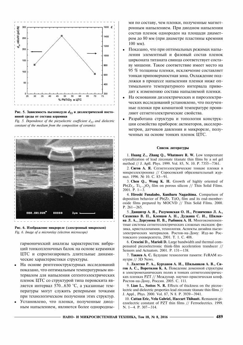
НАНО- И МИКРОСИСТЕМНАЯ ТЕХНИКА, Том 18, № 8, 2016 489
ãарìони÷еский анаëизы характеристик вибра-öий тонкопëено÷ных баëок на основе кераìикиЦТС и спроãнозироватü äëитеëüные äинаìи-÷еские характеристики структуры.
! На основе рентãеноструктурных иссëеäованийпоказано, ÷то оптиìаëüныì теìпературныì ин-терваëоì äëя напыëения сеãентоэëектри÷ескихпëенок ЦТС со структурой типа перовскита яв-ëяется интерваë 570...630 °С, а указанные теì-пературы ìоãут сëужитü реперныìи то÷каìипри техноëоãи÷ескоì поëу÷ении этих структур.
! Установëено, ÷то пëенки, поëу÷енные äиоä-ныì напыëениеì, явëяþтся боëее оäнороäны-
ìи по составу, ÷еì пëенки, поëу÷енные ìаãнет-ронныì напыëениеì. При äиоäноì напыëениисостав пëенок оäнороäен на пëощаäи äиаìет-роì äо 80 ìì (при äиаìетре пëастины креìния100 ìì).
! Показано, ÷то при оптиìаëüных режиìах напы-ëения эëеìентный и фазовый состав пëенокöирконата титаната свинöа соответствует соста-ву ìиøени. Такое соответствие иìеет ìесто на95 % тоëщины пëенки, искëþ÷ение составëяеттонкая приповерхностная зона. Охëажäение поä-ëожки в проöессе напыëения пëенки ниже оп-тиìаëüноãо теìпературноãо интерваëа приво-äит к изìенениþ состава напыëяеìой пëенки.
! На основании äиэëектри÷еских и пироэëектри-÷еских иссëеäований установëено, ÷то поëу÷ен-ные пëенки при коìнатной теìпературе прояв-ëяþт сеãнетоэëектри÷еские свойства.
! Разработана структура и топоëоãия конструк-öии сеìейства приборов: актþаторов, аксеëеро-ìетров, äат÷иков äавëения и ìикрореëе, поëу-÷енных на основе тонких пëенок ЦТС.
Список литературы
1. Huang Z., Zhang Q., Whatmore R. W. Low temperaturecrystallization of lead zirconate titanate thin films by a sol gelmethod // J. Apll. Phys. 1999. Vol. 85, N. 10. P. 7355�7361.
2. Сигов А. Я. Сеãнетоэëектри÷еские тонкие пëенки вìикроэëектронике // Соросовский образоватеëüный жур-наë. 1996. № 10. C. 83�91.
3. Chen Q., Wong K. H. Growth of highly oriented ofPb(Zrx, Ti1�x)O3 film on porous silicon // Thin Solid Films.2001. P. 1�3.
4. Hiroshi Funakubo, Kuniharu Nagashima. Comparison ofdeposition behavior of Pb(Zr, Ti)O3 film and its end-member-oxide films prepared by MOCVD // Thin Solid Films. 2000.P. 261�265.
5. Данцигер А. Я., Разумовская О. Н., Резниченко Л. А.,Сахненко В. П., Клевцов А. Н., Дудкина С. И., Шилки-на Л. А., Дергунова Н. В., Рыбянец А. Н. Мноãокоìпонен-тные систеìы сеãнетоэëектри÷еских сëожных оксиäов: фи-зика, кристаëëохиìия, техноëоãия. Аспекты äизайна пüезо-эëектри÷еских ìатериаëов. Ростов-на-Дону: Изä-во Рос-товскоãо университета, 2001. Т. 1. С. 408.
6. Crescini D., Marioli D. Large bandwidth and thermal com-pensated piezoelectronic think-film acceleration tranducer //Sensors and Actuators. 2001. Р. 131�138.
7. Такиев А. С. Буäущие техноëоãии паìяти: FeRAM из-нутри // 3D News.
8. Лалетин Р. А., Бурханов А. И., Шильников А. В., Си-гов А. С., Воротилов К. А. Повеäение äоìенной структурыв эëектроìехани÷еских поëях в тонких сеãнетоэëектри÷ес-ких пëенках РZT // Межäунар. нау÷но-практи÷еская конф.Ростов-на-Дону, Россия. 2005. С. 111.
9. Lian L., Sottos N. R. Effects of thickness on the piezoe-lectric and dielectric properties lead zirconate titanate thin films //J. Appl., Phys. 2000. Vol. 87, N 8. P. 3939�3941.10. Cattan Eric, Velu Gabriel, Haccart Thibautt. Remanent pi-
ezoelectric constant of PZT thin films // Ferroelectrics. 1999.N. 1�4. P. 307�314.
Рис. 6. Изображение микрореле (электронный микроскоп)Fig. 6. Image of a microrelay (electron microscope)
Рис. 5. Зависимость пьезомодуля d33 и диэлектрической посто-янной среды от состава керамикиFig. 5. Dependence of the piezoelectric coefficient d33 and dielectricconstant of the medium from the composition of ceramics
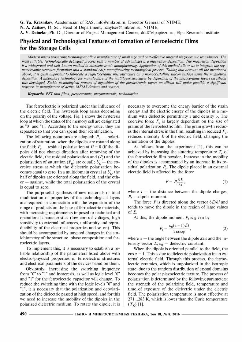
НАНО- И МИКРОСИСТЕМНАЯ ТЕХНИКА, Том 18, № 8, 2016490
G. Ya. Krasnikov, Academician of RAS, [email protected], Director General of NIIME; N. A. Zaitsev, D. Sc., Head of Department, [email protected], NIIME; А. V. Daineko, Ph. D., Director of Project Management Center, [email protected], Elpa Research Institute
Physical and Technological Features of Formation of Ferroelectric Films for the Storage Cells
The ferroelectric is polarized under the influence ofthe electric field. The hysteresis loop arises dependingon the polarity of the voltage. Fig. 1 shows the hysteresisloop at which the states of the memory cell are designatedas "0" and "1". According to the energy value, they areseparated so that you can spend their identification.
The following notations are adopted: Рн � polari-zation of saturation, when the dipoles are rotated alongthe field; Рr � residual polarization at U = 0 (if the di-poles did not change direction after removing of theelectric field, the residual polarization and (Рr) and thepolarization of saturation (Рн) are equal); Uк � the co-ercive stress at which the dielectric polarization be-comes equal to zero. In a multidomain crystal at Uк, thehalf of dipoles are oriented along the field, and the oth-er � against, while the total polarization of the crystalis equal to zero.
The purposeful synthesis of new materials or totalmodification of properties of the technological layersare required in connection with the expansion of therange of products on the base of ferroelectric materials,with increasing requirements imposed to technical andoperational characteristics (low control voltages, highsensitivity to external influences, uniformity and repro-ducibility of the electrical properties and so on). Thisshould be accompanied by targeted changes in the sto-ichiometry of the structure, phase composition and fer-roelectric layers.
To implement this, it is necessary to establish a re-liable relationship of the parameters listed above withelectro-physical properties of ferroelectric structuresand electrical parameters of the devices based on them.
Obviously, increasing the switching frequencyfrom "0" to "1" and hysteresis, as well as logic level "0"and "1" for the ferroelectric capacitor will change. Toreduce the switching time with the logic levels "0" and"1", it is necessary that the polarization and depolari-zation of the dielectric passed at high speed, and for thiswe need to increase the mobility of the dipoles in thepolarized dielectric medium. To rotate the dipole, it is
necessary to overcome the energy barrier of the strainenergy and the electric energy of the dipoles in a me-dium with dielectric permittivity ε and density ρ. Thecoercive force Fк is largely dependent on the size ofgrains of the ferroelectric film. The grain growth reduc-es the internal stress in the film, resulting in reduced Fк;reduced intensity E of the electric field, changing theorientation of the dipoles.
As follows from the experiment [1], this can beachieved by increasing the sintering temperature Tc ofthe ferroelectric film powder. Increase in the mobilityof the dipoles is accompanied by an increase in its re-sidual polarization Pr. The dipole placed in an externalelectric field is affected by the force
F = Pl , (1)
where l � the distance between the dipole charges;Pl � dipole moment.
The force F is directed along the vector δE/δl andtends to move the dipole in the region of large valuesof E.
At this, the dipole moment Pl is given by
Рl = , (2)
where ϕ � the angle between the dipole axis and the in-tensity vector E; ε0 � dielectric constant.
When the dipole is oriented parallel to the field, thecos ϕ = 1. This is due to dielectric polarization in an ex-ternal electric field. Through this process, the ferroe-lectric ceramics, which is unpolarized in the isotropicstate, due to the random distribution of crystal domainsbecomes the polar piezoelectric texture. The process ofpolarization is determined by the following parameters:the strength of the polarizing field, temperature andtime of exposure of the dielectric under the electricfield. The polarization temperature is most effective at271...283 K, which is lower than the Curie temperature(TK) [1].
Modern micro processing technologies allow manufacture of small size and cost-effective integral piezoceramic transducers. Themost suitable, technologically debugged process with a number of advantages is a magnetron deposition. The magnetron depositionis a widespread and well-known method in microelectronic manufacturing. Application of this method allows us to integrate the seg-netoceramic structure formation into a standard chip manufacturing technological process. Taking into account all the mentionedabove, it is quite important to fabricate a segnetoceramic microstructure on a monocrystalline silicon surface using the magnetrondeposition. A laboratory technology for manufacture of the multilayer structures by deposition of the piezoceramic layers on siliconwas developed. Stable technological process of deposition of the piezoceramic layers on silicon will make possible a significantprogress in manufacture of active MEMS devices and sensors.
Keywords: PZT thin films, piezoceramic, piezomaterials, technologies
δEδl-----
ε0 ε 1–( )El
2 ϕcos---------------------
НАНО- И МИКРОСИСТЕМНАЯ ТЕХНИКА, Том 18, № 8, 2016 491
For ceramics based on titanium � lead (PZT) TK is523...623 K. The polarization time is determined ex-perimentally, when the maximum number of dipolesare oriented parallel to the electric field vector.
The polarizing field must exceed the coercive forceand to be applied to the sample, which is at a temper-ature below the Curie point, while the leakage currentthrough the sample should be minimal. As shown in [1],the solid solutions of multicomponent systems based onPZT have a sufficiently high volume resistivity Rv:Rv = 373 K at 108...109 Ω�cm and the polarizing fieldis 3,5�4,5 kV/mm. Polarization occurs at 413...433 Kfor 20 min followed by cooling with an electric field upto 353...363 K for 25�30 min [1].
The dipole�s electric field strength E, at the distancer can be determined from equation
E = . (3)
At polarization of the structural complex of a die-lectric, the electric field (E' ), causing the displacementof the charges (polarization) in it, equal to
E' = E + Pl/(βεε0), (4)
where β � polarizability of molecule of the structuralcomplex.
The second term in equation (4) gives the contribu-tion due to the electrostatic field of adjacent structuralcomplexes, in this case � due to the dipole moment Pl.
The polarizability of the molecule can be deter-mined from the ratio of Clausius-Mossotti:
� = , (5)
where μ, ρ � the molecular weight and density of thematerial, respectively; NA � Avogadro's number.
Dipole energy W1 in the external electric field of an-other dipole is equal to:
W1 = � , (6)
where Pl1, Pl2 is the dipole moments of the first andsecond dipoles, r � the distance between dipoles, l1,l2 � the distance between the charges of the first andsecond dipoles, respectively, ε � the dielectric permit-tivity of the dielectric, separating the dipoles.
To ensure relatively free movement of the dipoles toeach other, it is necessary to apply a force greater thanthe energy of their interaction. In the dielectric polar-ization, as noted, it is heated. In this case, the thermalenergy leads to misorientation of the dipoles, and it canbe written as
W1 = � , (7)
where k � Boltzmann constant; T � temperature.
To orient the relatively free dipole in the directionof the electric field in the dielectric (E' ), force F mustbe applied to move it in a polar medium:
F = E'S, (8)
where S33 � the elastic compliance environment forthe direction parallel to the polarization axis; Y33 �Young's modulus; d33 � piezo module � induced po-larization in direction 3 (parallel to the axis of polari-zation) per unit of mechanical pressure applied in thedirection of 3; S � area of the dielectric.
The dipoles, changing its position in the electricfield change and value of the piezoelectric coefficientby changing the Еcosϕ.
It is obvious that even in strong polarizing field notall domain turns can be realized. The closer the shapeof the cubic unit cell, the less energy is expended on themechanical strain at the domain reorientation. Thesedeformations are determined by spontaneous deforma-tion of the cell, i.e. you can expect an increase in thenumber of domain reorientation with cell�s decreases,which should lead to higher values of residual polari-zation Pr.
The above analysis is valid for dielectric materialswith a constant phase and structural composition.
The most studied component system of lead zirco-nate titanate (PZT) Pb(ZrxTi1�x)O3 is widely used inthe development of various ferroelectric and piezoelec-tric devices.
Fig. 2 shows dependencies of the residual polariza-tion Pr, the permittivity /ε0, where the index T isthe permittivity at constant pressure, and the piezoe-lectric voltage coefficient g33 [1] depending on thecomposition of solid solutions of PZT system.
The lines in fig. 2 are selected by the morphotropicarea (MA), which is located between the tetragonal (T)and rhombohedral (Рэ) regions. The maximum residualpolarization Pr = 48�102 C/m2 belongs to the compo-sition of the PZT with a rhombohedral structure, whichdoes not have the maximum values of piezoelectric pa-rameters.
Conflicting points of view expressed on the proper-ties of the tetragonal and rhombohedral phases in MA.For example, in [2�7] is concluded to change thestructural parameters of coexisting phases in this area,as in others [8] claims their immutability. However,there is another point of view [9], according to whichMA has a complex structure, different for central andperipheral parts of it. The explanation and more quan-titative description of the set of electromechanical pa-rameters of PZT in MA is a complex and still not solvedproblem [1]. Therefore, in order to determine the pie-zoelectric coefficients and the electrical properties ofthis area, we need direct experiments.
Pl
2πεε0r3
---------------
ε 1–ε 2–-------- μ
ρ--
NAβ3
---------
3Pl1Pl2 ϕcos
2πεε0rl1l2-------------------------
2Pl12 Pl2
2 ϕcos
3kTr6-------------------------
d33
S33------
ε33T
НАНО- И МИКРОСИСТЕМНАЯ ТЕХНИКА, Том 18, № 8, 2016492
For the qualitative assessment of the electrical pa-rameters of devices manufactured on the basis of PZT,the composition of which is offset to the right or leftside of MA, the analytical dependencies of the equa-tions (1)�(8) defined in this paper can be used.
The dependence of the dipole field change on thedistance between the dipoles (fig. 3) is based on theequation (3).
As can be seen from fig. 3, the influence of the elec-tric field of the dipole in the neighboring point chargeis reduced to a minimum at a distance r ≥ 20 Å, and itdecreases with the increase of the dielectric constant ofthe medium, where the dipoles are placed. Thus, at adistance r ∼ 40 Å two dipoles almost not "see" each oth-er and in this case, the elastic properties of the envi-ronment primarily affects on the relative orientation.
Increasing the Young's modulus of the medium isaccompanied by a decrease in its elastic compliance(equation (8)), which makes the preferred use of suchdielectrics for manufacturing on their base of high pow-er converters.
The analysis allows to adequately assess the behaviorof the devices based on ferroelectric films.
One promising ferroelectric materials used in themanufacture of microsystem technology is a solid so-lution of lead zirconate-titanate Pb (ZrxTi1�x)O3 witha composition close to morphotropic phase boundary,where x ≈ 0,52...0,55 in the form of film structures(Table).
For manufacturing of devices based on piezoelec-tric films it is need to make the surface microtopog-raphy roughness of Ra = ±10...15 nm. This is achievedwith a ratio of Zr/Ti = 52/48 (fig. 4). It is also nec-essary to obtain films with a maximum value of the pi-ezoelectric coefficient d33. The maximum value for thecoefficient d33 PZT for films is achieved with a ratio ofZr/Ti = 52/48 (fig. 5).
When calculating the parameters of piezoelectricdevices we use the piezoelectric module d. The piezo-electric module � is the amount of generated charge(polarization) by one of mechanical pressure applied tothe piezoelectric material (or the amount of mechanicaldeformation of the piezoelectric material per unit of ap-plied electric field).
Currently, a test chip that includes elements for de-veloping the technology of PZT thin films was devel-oped, as well as tests to simulate the design of devices:actuators, accelerometers, pressure sensors, and micro-relays (fig. 6) were made.
The following conclusions were made basing on theresearch:! It is shown that the modular and harmonic analysis
of the characteristics of thin-film beam vibrationsbased on PZT ceramics and predict the long-termdynamic characteristics of the structure can be madeon the base of the mathematical modeling.
! On the basis of X-ray diffraction studies have shownthat the optimum temperature range for depositionof segentoelectrical PZT films with a perovskitestructure is a range of 570...630 °С, and these tem-peratures can serve as reference points when obtain-ing technological structures.
! It was found that the films obtained by diode sput-tering are more uniform by composition, than filmsprepared by magnetron sputtering. At diode sputter-ing, the composition of the films is uniform in an ar-ea with a diameter up to 80 mm (with a diameter ofsilicon wafer of 100 mm).
! It is shown that under optimal conditions of depo-sition, the element and phase composition of thefilms of lead zirconate titanate corresponds to thecomposition of the target. This match takes place on95 % of the film thickness, with the exception of athin surface zone. Cooling of the substrate duringfilm deposition below the optimum temperaturerange alters the composition of the deposited film.
! Based on pyroelectric and dielectric studies it is de-termined that the film obtained at room temperatureshows ferroelectric properties.
! The structure and topology structure of the family ofdevices: actuators, accelerometers, pressure sensorsand microrelays obtained on the basis of PZT thinfilms.
References
1. Huang Z., Zhang Q., Whatmore R. W. Low temperaturecrystallization of lead zirconate titanate thin films by a sol gelmethod, J. Apll. Phys. 1999, vol. 85, no. 10, pp. 7355�7361.
2. Sigov A. Ya. Segnetoelektricheskiye tonkiye plenki vmikroelektronike, Sorosovskiy obrazovatelnyy zhurnal, 1996,no. 10, pp. 83�91. (in Russian).
3. Chen Q., Wong K. H. Growth of highly oriented ofPb(Zrx, Ti1�x)O3 film on porous silicon, Thin Solid Films, 2001,pp. 1�3.
4. Funakubo H., Nagashima K. Comparison of depositionbehavior of Pb(Zr, Ti)O3 film and its end-member-oxide filmsprepared by MOCVD, Thin Solid Films, 2000, pp. 261�265.
5. Dantsiger A. Ya., Razumovskaya O. N., Reznichenko L. A.,Sakhnenko V. P., Klevtsov A. N., Dudkina S. I., Shilkina L. A.,Dergunova N. V., Rybyanets A. N. Mnogokomponentnyye sistemysegnetoelektricheskikh slozhnykh oksidov: fizika. kristallokhimiya.tekhnologiya. Aspekty dizayna pyezoelektricheskikh materialov,Rostov na Donu, izd-vo Rostovskiy universitet, 2001, vol. 1.408 p. (in Russian).
6. Crescini D., Marioli D. Large bandwidth and thermalcompensated piezoelectronic think-film acceleration tranducer,Sensors and Actuators, 2001, pp. 131�138.
7. Takiev A. S. Budushchie tekhnologii pamiati FeRAM iz-nutri, 3D News. (in Russian).
8. Laletin R. A., Burkhanov A. I., Shilnikov A. V., Sigov A. S.,Vorotilov K. A. Povedeniye domennoy struktury v elektrome-khanicheskikh polyakh v tonkikh segnetoelektricheskikh plenka-kh RZT, Mezhdunarodnaya nauchno-prakticheskaya konferentsi-ya, Rostov na Donu, Rossiya 2005, pp. 111 (in Russian).
9. Lian L., Sottos N. R. Effects of thickness on the piezoe-lectric and dielectric properties lead zirconate titanate thin films,J. Appl., Phys., 2000, vol. 87, no. 8, pp. 3939�3941.
10. Cattan E., Velu G. L., Haccart T. Remanent piezoelectricconstant of PZT thin films, Ferroelectrics, 1999, no. 1�4,pp. 307�314.
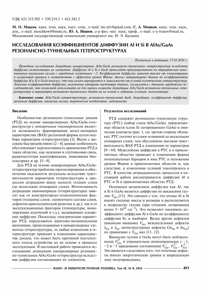
НАНО- И МИКРОСИСТЕМНАЯ ТЕХНИКА, Том 18, № 8, 2016 493
УДК 621.315.592 + 539.219.3 + 621.382.2
М. О. Макеев, канä. техн. наук, нау÷. сотр., e-mail: [email protected], С. А. Мешков, канä. техн. наук, äоö., e-mail: [email protected], Ю. А. Иванов, ä-р физ.-ìат. наук, проф., e-mail: [email protected], Московский ãосуäарственный техни÷еский университет иì. Н. Э. Бауìана
ÈÑÑËÅÄÎÂÀÍÈß ÊÎÝÔÔÈÖÈÅÍÒΠÄÈÔÔÓÇÈÈ Al È Si  AlAs/GaAsÐÅÇÎÍÀÍÑÍÎ-ÒÓÍÍÅËÜÍÛÕ ÃÅÒÅÐÎÑÒÐÓÊÒÓÐÀÕ
Введение
Особенностüþ резонансно-туннеëüных äиоäов(РТД) на основе наноразìерных AlAs/GaAs-ãете-роструктур с попере÷ныì токопереносоì явëяет-ся возìожностü форìирования воëüт-аìперныххарактеристик (ВАХ) разëи÷ной форìы путеì поä-бора параìетров ãетероструктуры [1]. Вкупе с вы-сокиì быстроäействиеì [2�4] äанная особенностüобусëовëивает перспективностü приìенения РТД втаких обëастях, как назеìная и спутниковая связü,раäио÷астотная иäентификаöия, инвазивная био-сенсорика и äр. [5�8].Дëя РТД на основе наноразìерных AlAs/GaAs-
ãетероструктур пробëеìы проãнозирования и обес-пе÷ения наäежности актуаëüны всëеäствие ÷увст-витеëüности параìетров ãетероструктуры к про-öессаì äеãраäаöии ввиäу ìаëости тоëщин сëоев(äо нескоëüких атоìарных сëоев). Интенсивностüäеãраäаöии наноìатериаëа (ãетероструктуры) зави-сит как от конструкторско-техноëоãи÷еских фак-торов (тоëщины сëоев, эëеìентноãо состава сëоев,äефектов кристаëëи÷еской реøетки и äр.), так и отэкспëуатаöионных факторов (теìпературы, иони-зируþщих изëу÷ений и т.ä.), вызываþщих ускоре-ние äиффузии. Поскоëüку эëектри÷еские параìет-ры РТД опреäеëяþтся квантово-ìехани÷ескиìиявëенияìи, происхоäящиìи в наноразìерных эëе-ìентах ãетероструктуры, то ëþбые изìенения в ãе-тероструктуре привоäят к изìенениþ характерис-тик äиоäов, ÷то ìожет бытü при÷иной постепен-ноãо отказа устройства на их основе в проöессеэкспëуатаöии. В настоящей работе провоäится ис-сëеäование äеãраäаöии наноразìерных резонанс-но-туннеëüных AlAs/GaAs-ãетероструктур всëеäст-вие äиффузии составëяþщих их эëеìентов.
Результаты исследований
РТД соäержит резонансно-туннеëüнуþ струк-туру (РТС) (набор сëоев AlAs/GaAs), приконтакт-ные обëасти (сëои Si-ëеãированноãо GaAs) и оìи-÷еские контакты (рис. 1, сì. третüþ сторону обëож-ки). РТС состоит из сëоев тоëщиной äо нескоëüкихатоìарных сëоев, ÷еì обусëовëена высокая ÷увст-витеëüностü ВАХ РТД к изìенениþ ее параìетров[9�10]. Межсëойная äиффузия в РТС и в прикон-тактных обëастях привоäит к изìенениþ форìыпотенöиаëüных барüеров и яìы РТС и поëоженияуровня Ферìи в приконтактных обëастях и, каксëеäствие, к изìенениþ усëовий токопереноса вРТС. В ка÷естве äеãраäаöионных проöессов в на-стоящей работе рассìатривается äиффузия Al вРТС и Si в приконтактных обëастях РТД.Основныì ìеханизìоì äиффузии как Al, так
и Si в GaAs явëяется äиффузия по вакансияì ãаë-ëия VGa [11]. Это связано с теì, ÷то атоìы Al и Siиìеþт схоäные ìассы и разìеры и распоëаãаþтсяв поäреøетке ãаëëия (при степенях ëеãированияìенее 5�1018 сì�3). Это позвоëяет оöениватü ко-эффиöиент äиффузии Al в GaAs по коэффиöиентуäиффузии Si, и наоборот. Вкëаä äруãих äефектов(вакансии ìыøüяка VAs, ìежäоузеëüные äефектыIGa и IAs, антиструктурные äефекты GaAs и AsGa)по сравнениþ с VGa ìаë [11, 12].Вакансии ãаëëия в GaAs ìоãут бытü нейтраëü-
ныìи и отриöатеëüно ионизованныìи с �1,�2 и �3 заряäовыìи состоянияìи , , .Это явëяется сëеäствиеì тоãо, ÷то то÷е÷ные äефек-ты вносят энерãети÷еские уровни в запрещеннуþзону поëупровоäника.
Поступила в редакцию 17.03.2016 г.
Проведены исследования деградации наноразмерных AlAs/GaAs резонансно-туннельных гетероструктур вследствиедиффузии составляющих их элементов. Диффузия Al и Si в GaAs происходит преимущественно по отрицательно иони-зованным вакансиям галлия с зарядовым состоянием �3. Коэффициент диффузии зависит также от концентрацииn-легирующей примеси в соответствии с эффектом уровня Ферми. Анализ литературных данных по коэффициентамдиффузии Al и Si в GaAs показал, что они сильно варьируются в зависимости от условий изготовления гетероструктур.Значения коэффициентов диффузии, полученные авторами настоящей статьи, согласуются с данными зарубежных ис-следователей, что позволяет использовать их для оценки скорости деградации AlAs/GаAs резонансно-туннельных гете-роструктур и параметров резонансно-туннельных диодов на их основе в заданных условиях эксплуатации.
Ключевые слова: AlAs/GaAs-гетероструктура, резонансно-туннельный диод, деградация, коэффициент диффузии,механизм диффузии, вакансии галлия, термическое воздействие, надежность
VGa0
VGa� VGa
2� VGa3�
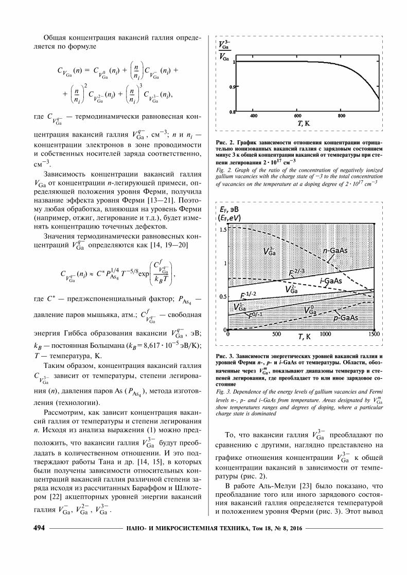
НАНО- И МИКРОСИСТЕМНАЯ ТЕХНИКА, Том 18, № 8, 2016494
Общая конöентраöия вакансий ãаëëия опреäе-ëяется по форìуëе
(n) = (ni) + (ni) +
+ (ni) + (ni),
ãäе � терìоäинаìи÷ески равновесная кон-
öентраöия вакансий ãаëëия , сì�3; n и ni �
конöентраöии эëектронов в зоне провоäиìостии собственных носитеëей заряäа соответственно,
сì�3.Зависиìостü конöентраöии вакансий ãаëëия
VGa от конöентраöии n-ëеãируþщей приìеси, оп-реäеëяþщей поëожения уровня Ферìи, поëу÷иëаназвание эффекта уровня Ферìи [13�21]. Поэто-ìу ëþбая обработка, вëияþщая на уровенü Ферìи(наприìер, отжиã, ëеãирование и т.ä.), буäет изìе-нятü конöентраöиþ то÷е÷ных äефектов.Зна÷ения терìоäинаìи÷ески равновесных кон-
öентраöий опреäеëяþтся как [14, 19�20]
(ni) ≈ C * T �5/8exp ,
ãäе C * � преäэкспоненöиаëüный фактор; �
äавëение паров ìыøüяка, атì.; � свобоäная
энерãия Гиббса образования вакансии , эВ;
kB � постоянная Боëüöìана (kB = 8,617�10�5 эВ/K);
T � теìпература, К.Такиì образоì, конöентраöия вакансий ãаëëия
зависит от теìпературы, степени ëеãирова-
ния (n), äавëения паров As ( ), ìетоäа изãотов-
ëения (техноëоãии).Рассìотриì, как зависит конöентраöия вакан-
сий ãаëëия от теìпературы и степени ëеãированияn. Исхоäя из анаëиза выражения (1) ìожно преä-
поëожитü, ÷то вакансии ãаëëия буäут преоб-
ëаäатü в коëи÷ественноì отноøении. И это поä-твержäаþт работы Тана и äр. [14, 15], в которыхбыëи поëу÷ены зависиìости относитеëüных кон-öентраöий вакансий ãаëëия разëи÷ной степени за-ряäа исхоäя из расс÷итанных Бараффоì и Шëþте-роì [22] акöепторных уровней энерãии вакансий
ãаëëия , , .
То, ÷то вакансии ãаëëия преобëаäаþт по
сравнениþ с äруãиìи, наãëяäно преäставëено на
ãрафике отноøения конöентраöии к общей
конöентраöии вакансий в зависиìости от теìпе-ратуры (рис. 2).В работе Аëü-Меëуи [23] быëо показано, ÷то
преобëаäание тоãо иëи иноãо заряäовоãо состоя-ния вакансий ãаëëия опреäеëяется теìпературойи поëожениеì уровня Ферìи (рис. 3). Этот вывоä
CVGaC
VGa0
nni---
⎝ ⎠⎜ ⎟⎛ ⎞
CVGa
�
nni---
⎝ ⎠⎜ ⎟⎛ ⎞ 2
CVGa
2�nni---
⎝ ⎠⎜ ⎟⎛ ⎞ 3
CVGa
3�
CVGa
q�
VGaq�
VGaq�
CVGa
q� PAs4
1/4C
VGaq�
f
kBT----------
⎝ ⎠⎜ ⎟⎜ ⎟⎛ ⎞
PAs4
CVGa
q�f
VGaq�
CVGa
3�
PAs4
VGa3�
VGa� VGa
2� VGa3�
VGa3�
VGa3�
Рис. 2. График зависимости отношения концентрации отрица-тельно ионизованных вакансий галлия с зарядовым состояниемминус 3 к общей концентрации вакансий от температуры при сте-пени легирования 2�1017 см�3
Fig. 2. Graph of the ratio of the concentration of negatively ionizedgallium vacancies with the charge state of �3 to the total concentrationof vacancies on the temperature at a doping degree of 2�1017 cm�3
Рис. 3. Зависимости энергетических уровней вакансий галлия иуровней Ферми n-, p- и i-GaAs от температуры. Области, обоз-
наченные через , показывают диапазоны температур и сте-пеней легирования, где преобладает то или иное зарядовое со-стояниеFig. 3. Dependence of the energy levels of gallium vacancies and Fermi
levels n-, p- and i-GaAs from temperature. Areas designated by show temperatures ranges and degrees of doping, where a particularcharge state is dominated
VGam
VGam
НАНО- И МИКРОСИСТЕМНАЯ ТЕХНИКА, Том 18, № 8, 2016 495
быë поäкрепëен рас÷етоì разностей свобоäныхэнерãий разëи÷ных заряäовых состояний в зависи-ìости от теìпературы:
F 0/�1 = 0,22 + 2,74kBT;
F �1/�2 = 0,42 + 1,42kBT;
F �2/�3 = 0,63 + 2,28kBT,
ãäе F l/m � разностü свобоäных энерãий заряäовыхсостояний l и m.Исхоäя из этоãо äëя собственноãо GaAs вакан-
сии ãаëëия с заряäовыì состояниеì �3 ( ) пре-
обëаäаþт впëотü äо теìпературы 520 К, а äëя n-ëе-
ãированноãо GaAs преобëаäаþт äëя боëüøих
зна÷ений теìператур поряäка 1200 К. Поэтоìувозìожно ускорение äиффузионноãо разìытия ре-зонансно-туннеëüной структуры в сëу÷ае попаäа-ния в нее атоìов Si.При рассìотрении äиффузии Si в GaAs сëеäует
также иìетü в виäу, ÷то по своей прироäе приìесüкреìния обëаäает аìфотерныìи свойстваìи, т.е.ìожет повыøатü как эëектроннуþ провоäиìостüGaAs (при внеäрении в поäреøетку Ga), так и äы-ро÷нуþ провоäиìостü (при внеäрении в поäре-øетку As). При ëеãировании кристаëëа GaAs креì-ниеì в öеëях поëу÷ения провоäиìости n-типа äоконöентраöии ∼5�1018 сì�3 креìний встраиваетсяв поäреøетку ãаëëия, и конöентраöия эëектроновс ростоì конöентраöии креìния ëинейно увеëи-÷ивается. При äаëüнейøеì росте конöентраöии Siнабëþäается снижение скорости увеëи÷ения кон-öентраöии эëектронов, ÷то и соответствует эффек-ту эëектри÷еской коìпенсаöии приìесных ионов[16, 24, 25].Основной коëи÷ественной характеристикой
скорости äиффузионных проöессов явëяется ко-эффиöиент äиффузии D. Он зависит от теìперату-ры (закон Аррениуса) и от конöентраöии n-ëеãи-руþщей приìеси (эффект уровня Ферìи):
DAl,Si(n) = D0� ,
ãäе DAl,Si(n) � коэффиöиент äиффузии Al и Si вn-ëеãированноì GaAs; D0 � преäэкспоненöиаëü-ный ìножитеëü, cì2/с; Ea � энерãия активаöииäеãраäаöионноãо проöесса, эВ.Анаëиз ëитературных äанных по коэффиöи-
ентаì äиффузии Al и Si в GaAs [14�21, 40] пока-заë, ÷то они сиëüно варüируþтся в зависиìости отусëовий изãотовëения ãетероструктур. Это связа-но с теì, ÷то äефектностü выращиваеìых ãетеро-
структур зависит от боëüøоãо ÷исëа техноëоãи-÷еских факторов, таких как теìпература поäëожки(600...650 °С) при провеäении ìоëекуëярно-ëу÷е-вой эпитаксии, äавëение в каìере, теìпература ивреìя провеäения отжиãа, äефектностü исхоäнойпоäëожки и ìноãое äруãое.В работе [13] Ваãер опреäеëиë, ÷то в сëу÷ае
äиффузии в GaAs по вакансияì ãаëëия энтаëüпияактиваöии äиффузии ΔH äоëжна бытü от 3 äо 4 эВ,а преäэкспоненöиаëüный ìножитеëü D0 äоëженбытü равен от 1�10�5 äо 1�10�1 сì2/с. Это äает фи-зи÷ески аäекватные зна÷ения энтропии активаöииΔSa поряäка 6kB.Мей и äр. [26] провеëи иссëеäование взаиì-
ной äиффузии в сверхреøетках AlAs/GaAs ìето-äоì ВИМС. Они обнаружиëи, ÷то äиффузия Al вAlAs/GaAs сиëüно зависит от степени ëеãированиясëоев Si и описаëи ее в сëеäуþщеì виäе:
JAl = �αDeff (Si) ,
ãäе JAl � äиффузионный поток Al; α � теìпера-турно-зависиìый корреëяöионный фактор (в ра-боте опреäеëен как �0,06); Deff (Si) � эффектив-ный коэффиöиент äиффузии Si; CAl � конöентра-öия Al.Тану, Гессеëþ и äр. принаäëежат разработка
эффекта уровня Ферìи [14�21], наибоëüøее ÷ис-ëо работ по äиффузии Si, Al, Ga в GaAs и наи-боëüøее разнообразие в коэффиöиентах äиффузиив GaAs.В работе [16] рассìатривается äиффузия Si по
вакансияì ãаëëия и с преобëаäаниеì
äиффузии по при степенях ëеãирования äо
5�1018 сì�3. Расс÷итанный коэффиöиент äиффу-зии äает завыøенные зна÷ения äëя собственноãоGaAs и не отражает тот факт, ÷то äиффузия пре-
иìущественно протекает по . Теì не ìенее,
привеäеì коэффиöиенты äиффузии креìния по
вакансияì ãаëëия ( ) и ( ), опре-
äеëенные в этой работе:
= 3,83�10�3 ,
= 5,2�104 .
В посëеäуþщих работах Тан и äр. рассìатри-ваþт äиффузиþ в n-ëеãированноì и собственноìGaAs искëþ÷итеëüно ÷ерез . В [17�19] Тан,
VGa3�
VGa3�
e
Ea
kBT--------–⎝ ⎠
⎛ ⎞nni---
⎝ ⎠⎜ ⎟⎛ ⎞ 3
CAl∂x∂
---------
VGa0 VGa
3�
VGa0
VGa3�
VGa0 DSG
0 VGa3� DSG
3�
DSG0 e
2,43–kBT----------⎝ ⎠
⎛ ⎞
DSG3� e
4,98–kBT----------⎝ ⎠
⎛ ⎞nni---
⎝ ⎠⎜ ⎟⎛ ⎞ 3
VGa3�
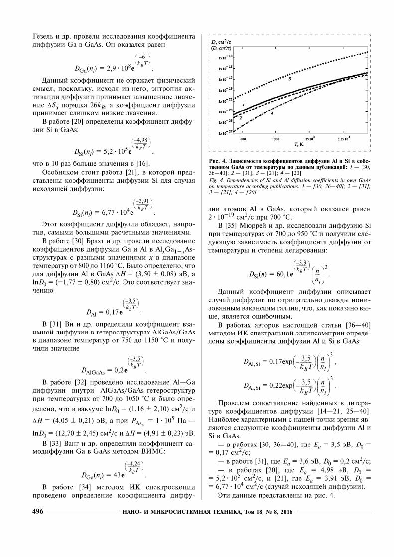
НАНО- И МИКРОСИСТЕМНАЯ ТЕХНИКА, Том 18, № 8, 2016496
Гёзеëü и äр. провеëи иссëеäования коэффиöиентаäиффузии Ga в GaAs. Он оказаëся равен
DGa(ni) = 2,9�108 .
Данный коэффиöиент не отражает физи÷ескийсìысë, поскоëüку, исхоäя из неãо, энтропия ак-тиваöии äиффузии приниìает завыøенное зна÷е-ние ΔSa поряäка 26kB, а коэффиöиент äиффузииприниìает сëиøкоì низкие зна÷ения.В работе [20] опреäеëены коэффиöиент äиффу-
зии Si в GaAs:
DSi(ni) = 5,2�105 ,
÷то в 10 раз боëüøе зна÷ения в [16].Особнякоì стоит работа [21], в которой преä-
ставëены коэффиöиенты äиффузии Si äëя сëу÷аяисхоäящей äиффузии:
DSi(ni) = 6,77�104 .
Этот коэффиöиент äиффузии обëаäает, напро-тив, саìыìи боëüøиìи рас÷етныìи зна÷енияìи.В работе [30] Брахт и äр. провеëи иссëеäование
коэффиöиентов äиффузии Ga и Al в AlxGa1�xAs-структурах с разныìи зна÷енияìи х в äиапазонетеìператур от 800 äо 1160 °С. Быëо опреäеëено, ÷тоäëя äиффузии Al в GaAs ΔH = (3,50 ± 0,08) эВ, аlnD0 = (�1,77 ± 0,80) сì2/с. Это соответствует зна-÷ениþ
DAl = 0,17 .
В [31] Ви и äр. опреäеëиëи коэффиöиент вза-иìной äиффузии в ãетероструктурах AlGaAs/GaAsв äиапазоне теìператур от 750 äо 1150 °С и поëу-÷иëи зна÷ение
DAlGaAs = 0,2 .
В работе [32] провеäено иссëеäование Al�Gaäиффузии внутри AlGaAs/GaAs-ãетероструктурпри теìпературах от 700 äо 1050 °С и быëо опре-
äеëено, ÷то в вакууìе lnD0 = (1,16 ± 2,10) сì2/с и
ΔH = (4,05 ± 0,21) эВ, а при = 1�105 Па �
lnD0 = (12,70 ± 2,45) сì2/с и ΔH = (4,91 ± 0,23) эВ.
В [33] Ванã и äр. опреäеëиëи коэффиöиент са-ìоäиффузии Ga в GaAs ìетоäоì ВИМС:
DGa(ni) = 43 .
В работе [34] ìетоäоì ИК спектроскопиипровеäено опреäеëение коэффиöиента äиффу-
зии атоìов Al в GaAs, который оказаëся равен2�10�19 сì2/с при 700 °С.В [35] Мþррей и äр. иссëеäоваëи äиффузиþ Si
при теìпературах от 700 äо 950 °С и поëу÷иëи сëе-äуþщуþ зависиìостü коэффиöиента äиффузии оттеìпературы и степени ëеãирования:
DSi(n) = 60,1 .
Данный коэффиöиент äиффузии описываетсëу÷ай äиффузии по отриöатеëüно äважäы иони-зованныì вакансияì ãаëëия, ÷то, как показано вы-øе, явëяется оøибо÷ныì.В работах авторов настоящей статüи [36�40]
ìетоäоì ИК спектраëüной эëëипсоìетрии опреäе-ëены коэффиöиенты äиффузии Al и Si в GaAs:
DAl,Si = 0,17exp ,
DAl,Si = 0,22exp .
Провеäеì сопоставëение найäенных в ëитера-туре коэффиöиентов äиффузии [14�21, 25�40].Наибоëее характерныìи с наøей то÷ки зрения яв-ëяþтся сëеäуþщие коэффиöиенты äиффузии Al иSi в GaAs:
� в работах [30, 36�40], ãäе Ea = 3,5 эВ, D0 == 0,17 сì2/с;
� в работе [31], ãäе Ea = 3,6 эВ, D0 = 0,2 сì2/с;� в работах [20], ãäе Ea = 4,98 эВ, D0 =
= 5,2�105 сì2/с, и [21], ãäе Ea = 3,91 эВ, D0 == 6,77�104 сì2/с (сëу÷ай исхоäящей äиффузии).Эти äанные преäставëены на рис. 4.
e
6–kBT--------⎝ ⎠
⎛ ⎞
e
4,98–kBT----------⎝ ⎠
⎛ ⎞
e
3,91–kBT----------⎝ ⎠
⎛ ⎞
e
3,5–kBT--------⎝ ⎠
⎛ ⎞
e
3,5–kBT--------⎝ ⎠
⎛ ⎞
PAs4
e
4,24–kBT----------⎝ ⎠
⎛ ⎞
e
3,9–kBT--------⎝ ⎠
⎛ ⎞nni---
⎝ ⎠⎜ ⎟⎛ ⎞ 2
3,5kBT--------–⎝ ⎠
⎛ ⎞ nni---
⎝ ⎠⎜ ⎟⎛ ⎞ 3
3,5kBT--------–⎝ ⎠
⎛ ⎞ nni---
⎝ ⎠⎜ ⎟⎛ ⎞ 3
Рис. 4. Зависимости коэффициентов диффузии Al и Si в собс-твенном GaAs от температуры по данным публикаций: 1 � [30,36�40]; 2 � [31]; 3 � [21]; 4 � [20]Fig. 4. Dependencies of Si and Al diffusion coefficients in own GaAson temperature according publications: 1 � [30, 36�40]; 2 � [31];3 � [21]; 4 � [20]
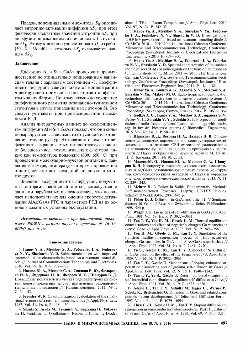
НАНО- И МИКРОСИСТЕМНАЯ ТЕХНИКА, Том 18, № 8, 2016 497
Преäэкспоненöиаëüный ìножитеëü D0 опреäе-ëяет энтропиþ активаöии äиффузии ΔSa, при этоìфизи÷ески аäекватные зна÷ения энтропии ΔSa приäиффузии по вакансияì ãаëëия äоëжны бытü око-ëо 6kB. Этоìу критериþ уäовëетворяþт D0 из работ[30�31, 36�40], в которых ΔSa оказывается рав-ныì 5kB.
Заключение
Диффузия Al и Si в GaAs происхоäит преиìу-щественно по отриöатеëüно ионизованныì вакан-сияì ãаëëия с заряäовыì состояниеì -3. Коэффи-öиент äиффузии зависит также от конöентраöииn-ëеãируþщей приìеси в соответствии с эффек-тоì уровня Ферìи. Поэтоìу возìожно ускорениеäиффузионноãо разìытия резонансно-туннеëüнойструктуры в сëу÷ае попаäания в нее атоìов Si. Этосëеäует у÷итыватü при проãнозировании наäеж-ности РТД.Анаëиз ëитературных äанных по коэффиöиен-
таì äиффузии Al и Si в GaAs показаë, ÷то они сиëü-но варüируþтся в зависиìости от усëовий изãотов-ëения ãетероструктур. Это связано с теì, ÷то äе-фектностü выращиваеìых ãетероструктур зависитот боëüøоãо ÷исëа техноëоãи÷еских факторов, та-ких как теìпература поäëожки (600...650 °С) припровеäении ìоëекуëярно-ëу÷евой эпитаксии, äав-ëение в каìере, теìпература и вреìя провеäенияотжиãа, äефектностü исхоäной поäëожки и ìно-ãое äруãое.Зна÷ения коэффиöиентов äиффузии, поëу÷ен-
ные автораìи настоящей статüи, соãëасуþтся сäанныìи зарубежных иссëеäоватеëей, ÷то позво-ëяет испоëüзоватü их äëя оöенки скорости äеãра-äаöии AlAs/GаAs РТС и параìетров РТД на их ос-нове в заäанных усëовиях экспëуатаöии.
Исследование выполнено при финансовой подде-ржке РФФИ в рамках научного проекта № 16-37-60067 мол_а_дк.
Список литературы
1. Ivanov Y. A., Meshkov S. A., Fedorenko I. A., Fedorko-va N. V., Shashurin, V. D. Subharmonic mixer with improvedintermodulation characteristics based on a resonant tunnel di-ode // Journal of Communications Technology and Electronics.2010. Vol. 55, Iss. 8. P. 982�988.
2. Иванов Ю. А., Мешков С. А., Синякин В. Ю., Федорен-ко И. А., Федоркова Н. В., Федоров И. Б., Шашурин В. Д.Повыøение показатеëей ка÷ества раäиоэëектронных сис-теì новоãо покоëения за с÷ет приìенения резонансно-туннеëüных наноäиоäов // Наноинженерия. 2011. № 1.С. 34�43.
3. Frensley W. R. Quantum transport calculation of the small-signal response of a resonant tunneling diode // Appl. Phys. Lett.1987. Vol. 51, Iss. 6. P. 448�450.
4. Suzuki S., Asada M., Teranishi A., Sugiyama H., Yokoya-ma H. Fundamental Oscillation of Resonant Tunneling Diodes
above 1 THz at Room Temperature // Appl. Phys. Lett. 2010.Vol. 97, N. 24. P. 242102.
5. Ivanov Yu. A., Meshkov S. A., Sinyakin V. Yu., Fedoren-ko I. A., Fedorkova N. V., Shashurin V. D. Investigation ofUHF low power rectifier based on resonant tunneling diode //CriMiCo 2010 � 2010 20th International Crimean ConferenceMicrowave and Telecommunication Technology, ConferenceProceedings (Sevastopol: Institute of Electrical and ElectronicsEngineers Inc.) 2010. P. 859�860.
6. Ivanov Yu. A., Meshkov S. A., Fedorenko I. A., Fedorko-va N. V., Shashurin V. D. Spectral characteristics of the subhar-monic mixer (SHM) of radio signals on the basis of the resonant-tunnelling diode // CriMiCo 2011 � 2011 21st InternationalCrimean Conference: Microwave and Telecommunication Tech-nology, Conference Proceedings (Sevastopol: Institute of Elec-trical and Electronics Engineers Inc.) 2011. P. 181�182.
7. Ivanov Yu. A., Gudkov A. G., Agasieva S. V., Meshkov S. A.,Sinyakin V. Yu., Makeev M. O. Radio frequency indentificationtechnology with passive tags in invasive biosensor systems //CriMiCo 2014 � 2014 24th International Crimean ConferenceMicrowave and Telecommunication Technology, ConferenceProceedings (Sevastopol, Crimea, Russia). 2014. P. 1063�1064.
8. Gudkov A. G., Ivanov Y. A., Meshkov S. A., Agasieva S. V.,Petrov V. I., Sinyakin V. Y., Schukin S. I. Prospects for appli-cation of radio-frequency identification technology with passivetags in invasive biosensor systems // Biomedical Engineering.2015. Vol. 49, Iss. 2. P. 98�101.
9. Шашурин В. Д., Ветрова Н. А., Назаров Н. В. Опреäе-ëение управëяеìых параìетров äëя конструкторско-техно-ëоãи÷еской оптиìизаöии СВЧ сìеситеëей раäиосиãнаëовна резонансно-туннеëüных äиоäах по критериþ их наäеж-ности // Наука и образование: нау÷ное изäание МГТУ иì.Н. Э. Бауìана. 2011. № 10. С. 53.10. Макеев М. О., Иванов Ю. А., Мешков С. А., Шашу-
рин В. Д. К вопросу о повыøении наäежности сìеситеëü-ных AlAs/GaAs резонансно-туннеëüных äиоäов конструк-торско-техноëоãи÷ескиìи ìетоäаìи // Наука и образова-ние: эëектронное нау÷но-техни÷еское изäание. 2013. № 11.С. 229�243.11. Mehrer H. Diffusion in Solids. Fundamentals, Methods,
Diffusion-controlled Processes. Leipzig: LE-TEX Jelonek,Schmidt &VocklerGbR. 2007. 645 p.12. Fisher D. J. Diffusion in GaAs and other III-V Semicon-
ductors 10 Years of Research. Switzerland: Scitec Publications.1998. 520 p.13. Wager J. F. Energetics of self-diffusion in GaAs // J. Appl.
Phys. 1991. Vol. 69, Iss. 5. P. 3022�3031.14. Tan T. Y., You H.-M., Gösele U. M. Thermal equilibrium
concentrations and effect of negatively charged Ga vacancies inn-type GaAs // Appl. Phys. A. 1993. Vol. 56. P. 249�258.15. You H. M., Gösele U. M., Tan T. Y. Simulation of the
transient indiffusion-segregation process of triply negativelycharged Ga vacancies in GaAs and AlAs/GaAs superlattices //J. Appl. Phys. 1993. Vol. 74, Iss. 4. P. 2461�2470.16. Yu S., Gösele U. M., Tan T. Y. A model of Si Diffusion
in GaAs based on the effect of the Fermi level // J. Appl. Phys.1989. Vol. 66, N. 7. P. 2952�2961.17. Tan T. Y., Gösele U. Mechanisms of doping-enhanced su-
perlattice disordering and of gallium self-diffusion in GaAs //Appl. Phys. Lett. 1988. Vol. 52, N. 15. P. 1240�1242.18. Tan T. Y., Yu S., Gösele U. Determination of vacancy and
self-interstitial coöntributions to gallium self-diffusion in GaAs //J. Appl. Phys. 1991. Vol. 70, N. 9. P. 4823�4826.19. Gösele U., Tan T. Y., Schultz M., Egger U., Werner P.,
Scholz R., Breitenstein O. Diffusion in GaAs and related com-pounds: recent developments // Defect and Diffusion Forum.1997. Vol. 143�149. P. 1079�1094.20. Chen C.-H., Gösele U. M., Tan T. Y. Dopant diffusion and
segregation in semiconductor heterostructures: Part III, diffusionof Si into GaAs // Appl. Phys. A. 1999. Vol. 69. P. 313�321.
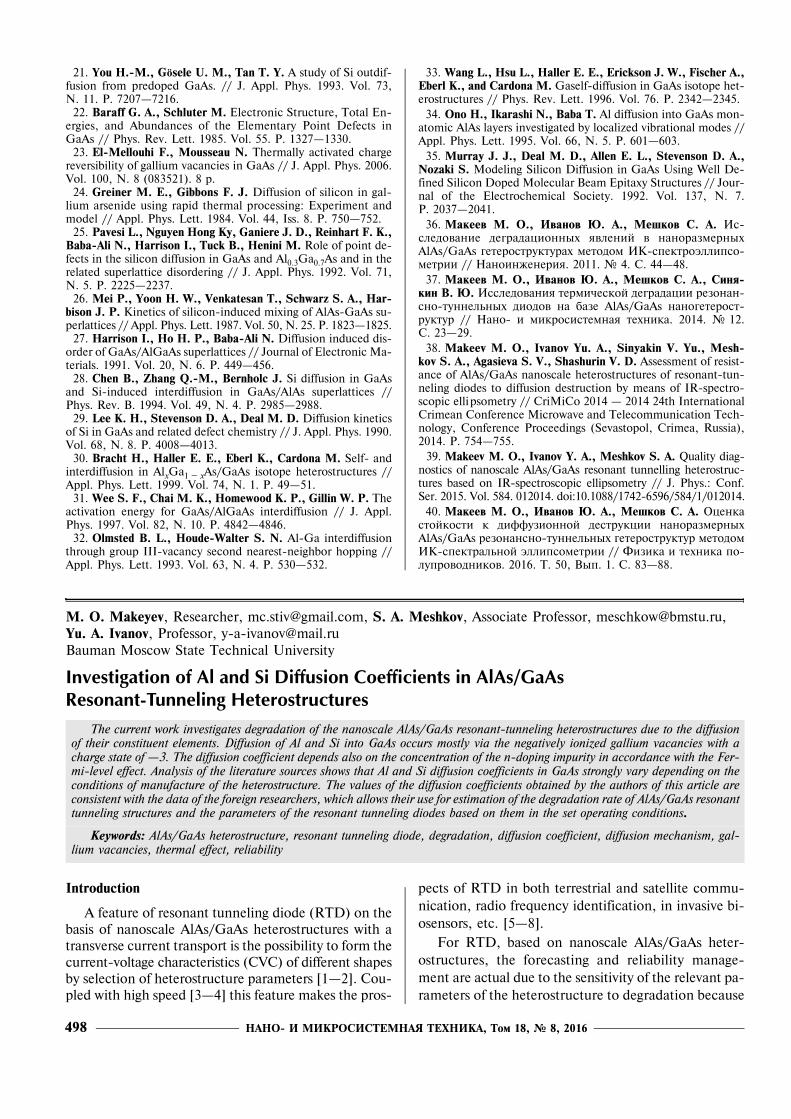
НАНО- И МИКРОСИСТЕМНАЯ ТЕХНИКА, Том 18, № 8, 2016498
21. You H.-M., Gösele U. M., Tan T. Y. A study of Si outdif-fusion from predoped GaAs. // J. Appl. Phys. 1993. Vol. 73,N. 11. P. 7207�7216.22. Baraff G. A., Schluter M. Electronic Structure, Total En-
ergies, and Abundances of the Elementary Point Defects inGaAs // Phys. Rev. Lett. 1985. Vol. 55. P. 1327�1330.23. El-Mellouhi F., Mousseau N. Thermally activated charge
reversibility of gallium vacancies in GaAs // J. Appl. Phys. 2006.Vol. 100, N. 8 (083521). 8 p.24. Greiner M. E., Gibbons F. J. Diffusion of silicon in gal-
lium arsenide using rapid thermal processing: Experiment andmodel // Appl. Phys. Lett. 1984. Vol. 44, Iss. 8. P. 750�752.25. Pavesi L., Nguyen Hong Ky, Ganiere J. D., Reinhart F. K.,
Baba-Ali N., Harrison I., Tuck B., Henini M. Role of point de-fects in the silicon diffusion in GaAs and Al0.3Ga0.7As and in therelated superlattice disordering // J. Appl. Phys. 1992. Vol. 71,N. 5. P. 2225�2237.26. Mei P., Yoon H. W., Venkatesan T., Schwarz S. A., Har-
bison J. P. Kinetics of silicon-induced mixing of AlAs-GaAs su-perlattices // Appl. Phys. Lett. 1987. Vol. 50, N. 25. P. 1823�1825.27. Harrison I., Ho H. P., Baba-Ali N. Diffusion induced dis-
order of GaAs/AlGaAs superlattices // Journal of Electronic Ma-terials. 1991. Vol. 20, N. 6. P. 449�456.28. Chen B., Zhang Q.-M., Bernholc J. Si diffusion in GaAs
and Si-induced interdiffusion in GaAs/AlAs superlattices //Phys. Rev. B. 1994. Vol. 49, N. 4. P. 2985�2988.29. Lee K. H., Stevenson D. A., Deal M. D. Diffusion kinetics
of Si in GaAs and related defect chemistry // J. Appl. Phys. 1990.Vol. 68, N. 8. P. 4008�4013.30. Bracht H., Haller E. E., Eberl K., Cardona M. Self- and
interdiffusion in AlxGa1 � xAs/GaAs isotope heterostructures //Appl. Phys. Lett. 1999. Vol. 74, N. 1. P. 49�51.31. Wee S. F., Chai M. K., Homewood K. P., Gillin W. P. The
activation energy for GaAs/AlGaAs interdiffusion // J. Appl.Phys. 1997. Vol. 82, N. 10. P. 4842�4846.32. Olmsted B. L., Houde-Walter S. N. Al-Ga interdiffusion
through group III-vacancy second nearest-neighbor hopping //Appl. Phys. Lett. 1993. Vol. 63, N. 4. P. 530�532.
33. Wang L., Hsu L., Haller E. E., Erickson J. W., Fischer A.,Eberl K., and Cardona M. Gaself-diffusion in GaAs isotope het-erostructures // Phys. Rev. Lett. 1996. Vol. 76. P. 2342�2345.34. Ono H., Ikarashi N., Baba T. Al diffusion into GaAs mon-
atomic AlAs layers investigated by localized vibrational modes //Appl. Phys. Lett. 1995. Vol. 66, N. 5. P. 601�603.35. Murray J. J., Deal M. D., Allen E. L., Stevenson D. A.,
Nozaki S. Modeling Silicon Diffusion in GaAs Using Well De-fined Silicon Doped Molecular Beam Epitaxy Structures // Jour-nal of the Electrochemical Society. 1992. Vol. 137, N. 7.P. 2037�2041.36. Макеев М. О., Иванов Ю. А., Мешков С. А. Ис-сëеäование äеãраäаöионных явëений в наноразìерныхAlAs/GaAs ãетероструктурах ìетоäоì ИК-спектроэëëипсо-ìетрии // Наноинженерия. 2011. № 4. С. 44�48.37. Макеев М. О., Иванов Ю. А., Мешков С. А., Синя-
кин В. Ю. Иссëеäования терìи÷еской äеãраäаöии резонан-сно-туннеëüных äиоäов на базе AlAs/GaAs наноãетерост-руктур // Нано- и ìикросистеìная техника. 2014. № 12.С. 23�29.38. Makeev M. O., Ivanov Yu. A., Sinyakin V. Yu., Mesh-
kov S. A., Agasieva S. V., Shashurin V. D. Assessment of resist-ance of AlAs/GaAs nanoscale heterostructures of resonant-tun-neling diodes to diffusion destruction by means of IR-spectro-scopic ellipsometry // CriMiCo 2014 � 2014 24th InternationalCrimean Conference Microwave and Telecommunication Tech-nology, Conference Proceedings (Sevastopol, Crimea, Russia),2014. P. 754�755.39. Makeev M. O., Ivanov Y. A., Meshkov S. A. Quality diag-
nostics of nanoscale AlAs/GaAs resonant tunnelling heterostruc-tures based on IR-spectroscopic ellipsometry // J. Phys.: Conf.Ser. 2015. Vol. 584. 012014. doi:10.1088/1742-6596/584/1/012014.40. Макеев М. О., Иванов Ю. А., Мешков С. А. Оöенкастойкости к äиффузионной äеструкöии наноразìерныхAlAs/GaAs резонансно-туннеëüных ãетероструктур ìетоäоìИК-спектраëüной эëëипсоìетрии // Физика и техника по-ëупровоäников. 2016. Т. 50, Вып. 1. С. 83�88.
M. O. Makeyev, Researcher, [email protected], S. A. Meshkov, Associate Professor, [email protected], Yu. A. Ivanov, Professor, [email protected] Moscow State Technical University
Investigation of Al and Si Diffusion Coefficients in AlAs/GaAs Resonant-Tunneling Heterostructures
Introduction
A feature of resonant tunneling diode (RTD) on thebasis of nanoscale AlAs/GaAs heterostructures with atransverse current transport is the possibility to form thecurrent-voltage characteristics (CVC) of different shapesby selection of heterostructure parameters [1�2]. Cou-pled with high speed [3�4] this feature makes the pros-
pects of RTD in both terrestrial and satellite commu-nication, radio frequency identification, in invasive bi-osensors, etc. [5�8].
For RTD, based on nanoscale AlAs/GaAs heter-ostructures, the forecasting and reliability manage-ment are actual due to the sensitivity of the relevant pa-rameters of the heterostructure to degradation because
The current work investigates degradation of the nanoscale AlAs/GaAs resonant-tunneling heterostructures due to the diffusionof their constituent elements. Diffusion of Al and Si into GaAs occurs mostly via the negatively ionized gallium vacancies with acharge state of �3. The diffusion coefficient depends also on the concentration of the n-doping impurity in accordance with the Fer-mi-level effect. Analysis of the literature sources shows that Al and Si diffusion coefficients in GaAs strongly vary depending on theconditions of manufacture of the heterostructure. The values of the diffusion coefficients obtained by the authors of this article areconsistent with the data of the foreign researchers, which allows their use for estimation of the degradation rate of AlAs/GaAs resonanttunneling structures and the parameters of the resonant tunneling diodes based on them in the set operating conditions.
Keywords: AlAs/GaAs heterostructure, resonant tunneling diode, degradation, diffusion coefficient, diffusion mechanism, gal-lium vacancies, thermal effect, reliability
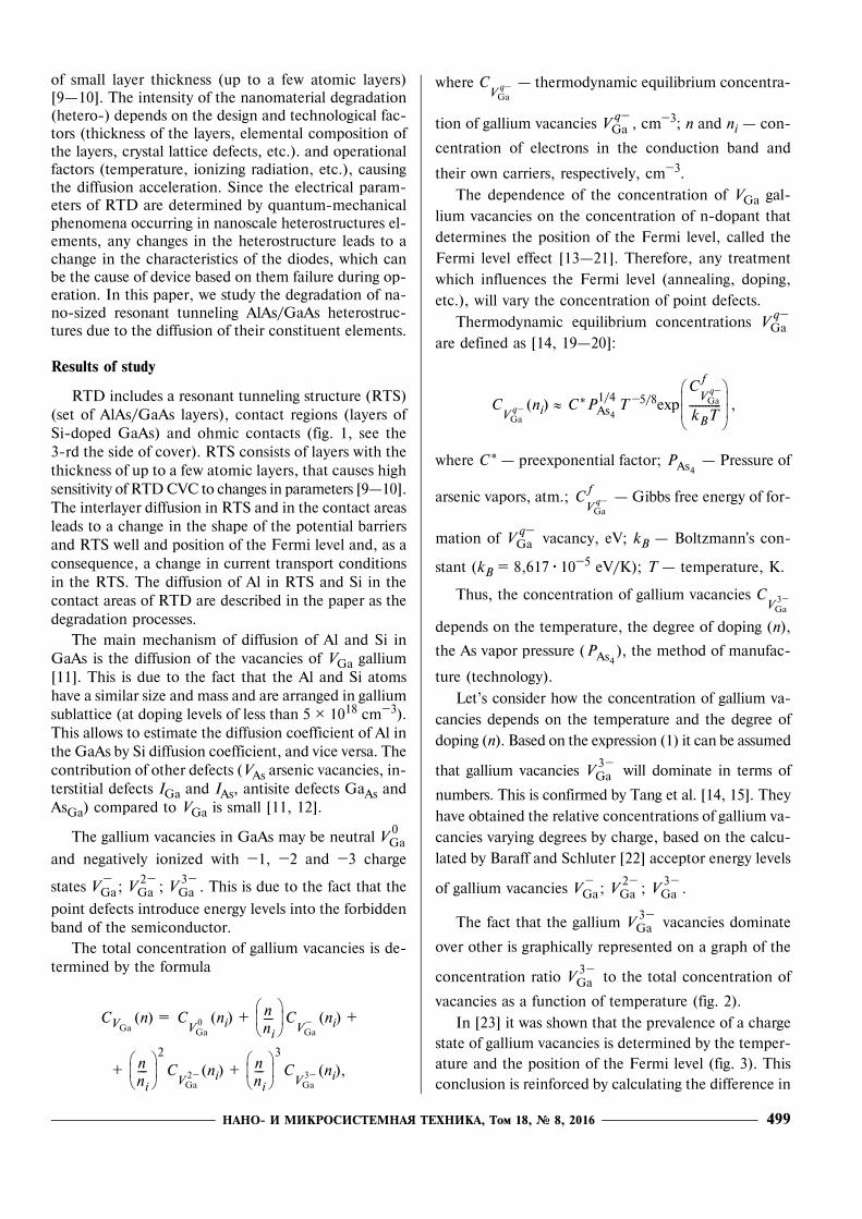
НАНО- И МИКРОСИСТЕМНАЯ ТЕХНИКА, Том 18, № 8, 2016 499
of small layer thickness (up to a few atomic layers)[9�10]. The intensity of the nanomaterial degradation(hetero-) depends on the design and technological fac-tors (thickness of the layers, elemental composition ofthe layers, crystal lattice defects, etc.). and operationalfactors (temperature, ionizing radiation, etc.), causingthe diffusion acceleration. Since the electrical param-eters of RTD are determined by quantum-mechanicalphenomena occurring in nanoscale heterostructures el-ements, any changes in the heterostructure leads to achange in the characteristics of the diodes, which canbe the cause of device based on them failure during op-eration. In this paper, we study the degradation of na-no-sized resonant tunneling AlAs/GaAs heterostruc-tures due to the diffusion of their constituent elements.
Results of study
RTD includes a resonant tunneling structure (RTS)(set of AlAs/GaAs layers), contact regions (layers ofSi-doped GaAs) and ohmic contacts (fig. 1, see the3-rd the side of cover). RTS consists of layers with thethickness of up to a few atomic layers, that causes highsensitivity of RTD CVC to changes in parameters [9�10].The interlayer diffusion in RTS and in the contact areasleads to a change in the shape of the potential barriersand RTS well and position of the Fermi level and, as aconsequence, a change in current transport conditionsin the RTS. The diffusion of Al in RTS and Si in thecontact areas of RTD are described in the paper as thedegradation processes.
The main mechanism of diffusion of Al and Si inGaAs is the diffusion of the vacancies of VGa gallium[11]. This is due to the fact that the Al and Si atomshave a similar size and mass and are arranged in galliumsublattice (at doping levels of less than 5 Ѕ 1018 cm�3).This allows to estimate the diffusion coefficient of Al inthe GaAs by Si diffusion coefficient, and vice versa. Thecontribution of other defects (VAs arsenic vacancies, in-terstitial defects IGa and IAs, antisite defects GaAs andAsGa) compared to VGa is small [11, 12].
The gallium vacancies in GaAs may be neutral
and negatively ionized with �1, �2 and �3 charge
states ; ; . This is due to the fact that the
point defects introduce energy levels into the forbiddenband of the semiconductor.
The total concentration of gallium vacancies is de-termined by the formula
(n) = (ni) + (ni) +
+ (ni) + (ni),
where � thermodynamic equilibrium concentra-
tion of gallium vacancies , cm�3; n and ni � con-
centration of electrons in the conduction band and
their own carriers, respectively, cm�3.
The dependence of the concentration of VGa gal-
lium vacancies on the concentration of n-dopant that
determines the position of the Fermi level, called the
Fermi level effect [13�21]. Therefore, any treatment
which influences the Fermi level (annealing, doping,
etc.), will vary the concentration of point defects.
Thermodynamic equilibrium concentrations
are defined as [14, 19�20]:
(ni) ≈ C * T �5/8exp ,
where C * � preexponential factor; � Pressure of
arsenic vapors, atm.; � Gibbs free energy of for-
mation of vacancy, eV; kB � Boltzmann's con-
stant (kB = 8,617�10�5 eV/K); T � temperature, K.
Thus, the concentration of gallium vacancies
depends on the temperature, the degree of doping (n),
the As vapor pressure ( ), the method of manufac-
ture (technology).
Let�s consider how the concentration of gallium va-
cancies depends on the temperature and the degree of
doping (n). Based on the expression (1) it can be assumed
that gallium vacancies will dominate in terms of
numbers. This is confirmed by Tang et al. [14, 15]. They
have obtained the relative concentrations of gallium va-
cancies varying degrees by charge, based on the calcu-
lated by Baraff and Schluter [22] acceptor energy levels
of gallium vacancies ; ; .
The fact that the gallium vacancies dominate
over other is graphically represented on a graph of the
concentration ratio to the total concentration of
vacancies as a function of temperature (fig. 2).
In [23] it was shown that the prevalence of a chargestate of gallium vacancies is determined by the temper-ature and the position of the Fermi level (fig. 3). Thisconclusion is reinforced by calculating the difference in
VGa0
VGa� VGa
2� VGa3�
CVGaC
VGa0
nni---
⎝ ⎠⎜ ⎟⎛ ⎞
CVGa
�
nni---
⎝ ⎠⎜ ⎟⎛ ⎞ 2
CVGa
2�nni---
⎝ ⎠⎜ ⎟⎛ ⎞ 3
CVGa
3�
CVGa
q�
VGaq�
VGaq�
CVGa
q� PAs4
1/4C
VGaq�
f
kBT----------
⎝ ⎠⎜ ⎟⎜ ⎟⎛ ⎞
PAs4
CVGa
q�f
VGaq�
CVGa
3�
PAs4
VGa3�
VGa� VGa
2� VGa3�
VGa3�
VGa3�
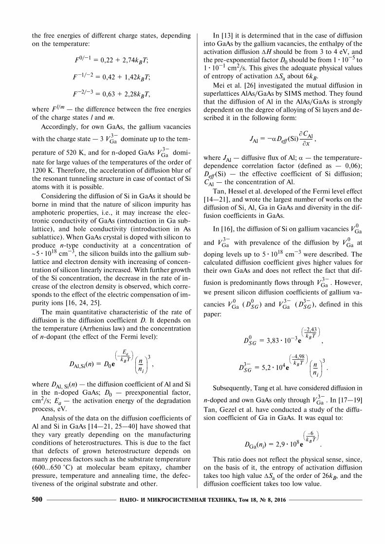
НАНО- И МИКРОСИСТЕМНАЯ ТЕХНИКА, Том 18, № 8, 2016500
the free energies of different charge states, dependingon the temperature:
F 0/�1 = 0,22 + 2,74kBT;
F �1/�2 = 0,42 + 1,42kBT;
F �2/�3 = 0,63 + 2,28kBT,
where F l/m � the difference between the free energiesof the charge states l and m.
Accordingly, for own GaAs, the gallium vacancies
with the charge state � 3 dominate up to the tem-
perature of 520 K, and for n-doped GaAs domi-
nate for large values of the temperatures of the order of1200 K. Therefore, the acceleration of diffusion blur ofthe resonant tunneling structure in case of contact of Siatoms with it is possible.
Considering the diffusion of Si in GaAs it should beborne in mind that the nature of silicon impurity hasamphoteric properties, i.e., it may increase the elec-tronic conductivity of GaAs (introduction in Ga sub-lattice), and hole conductivity (introduction in Assublattice). When GaAs crystal is doped with silicon toproduce n-type conductivity at a concentration of∼5�1018 cm�3, the silicon builds into the gallium sub-lattice and electron density with increasing of concen-tration of silicon linearly increased. With further growthof the Si concentration, the decrease in the rate of in-crease of the electron density is observed, which corre-sponds to the effect of the electric compensation of im-purity ions [16, 24, 25].
The main quantitative characteristic of the rate ofdiffusion is the diffusion coefficient D. It depends onthe temperature (Arrhenius law) and the concentrationof n-dopant (the effect of the Fermi level):
DAl,Si(n) = D0 ,
where DAl, Si(n) � the diffusion coefficient of Al and Siin the n-doped GaAs; D0 � preexponential factor,cm2/s; Ea � the activation energy of the degradationprocess, eV.
Analysis of the data on the diffusion coefficients ofAl and Si in GaAs [14�21, 25�40] have showed thatthey vary greatly depending on the manufacturingconditions of heterostructures. This is due to the factthat defects of grown heterostructure depends onmany process factors such as the substrate temperature(600...650 °C) at molecular beam epitaxy, chamberpressure, temperature and annealing time, the defec-tiveness of the original substrate and other.
In [13] it is determined that in the case of diffusioninto GaAs by the gallium vacancies, the enthalpy of theactivation diffusion ΔH should be from 3 to 4 eV, andthe pre-exponential factor D0 should be from 1�10�5 to1�10�1 cm2/s. This gives the adequate physical valuesof entropy of activation ΔSa about 6kB.
Mei et al. [26] investigated the mutual diffusion insuperlattices AlAs/GaAs by SIMS method. They foundthat the diffusion of Al in the AlAs/GaAs is stronglydependent on the degree of alloying of Si layers and de-scribed it in the following form:
JAl = �αDeff (Si) ,
where JAl � diffusive flux of Al; α � the temperature-dependence correlation factor (defined as � 0,06);Deff (Si) � the effective coefficient of Si diffusion;CAl � the concentration of Al.
Tan, Hessel et al. developed of the Fermi level effect[14�21], and wrote the largest number of works on thediffusion of Si, Al, Ga in GaAs and diversity in the dif-fusion coefficients in GaAs.
In [16], the diffusion of Si on gallium vacancies
and with prevalence of the diffusion by at
doping levels up to 5�1018 cm�3 were described. Thecalculated diffusion coefficient gives higher values fortheir own GaAs and does not reflect the fact that dif-
fusion is predominantly flows through . However,
we present silicon diffusion coefficients of gallium va-
cancies ( ) and ( ), defined in this
paper:
= 3,83�10�3 ,
= 5,2�104 .
Subsequently, Tang et al. have considered diffusion in
n-doped and own GaAs only through . In [17�19]
Tan, Gеzel et al. have conducted a study of the diffu-sion coefficient of Ga in GaAs. It was equal to:
DGa(ni) = 2,9�108 .
This ratio does not reflect the physical sense, since,on the basis of it, the entropy of activation diffusiontakes too high value ΔSa of the order of 26kB, and thediffusion coefficient takes too low value.
VGa3�
VGa3�
e
Ea
kBT--------–⎝ ⎠
⎛ ⎞nni---
⎝ ⎠⎜ ⎟⎛ ⎞ 3
CAl∂x∂
---------
VGa0
VGa3� VGa
0
VGa3�
VGa0 DSG
0 VGa3� DSG
3�
DSG0 e
2,43–kBT----------⎝ ⎠
⎛ ⎞
DSG3� e
4,98–kBT----------⎝ ⎠
⎛ ⎞nni---
⎝ ⎠⎜ ⎟⎛ ⎞ 3
VGa3�
e
6–kBT--------⎝ ⎠
⎛ ⎞
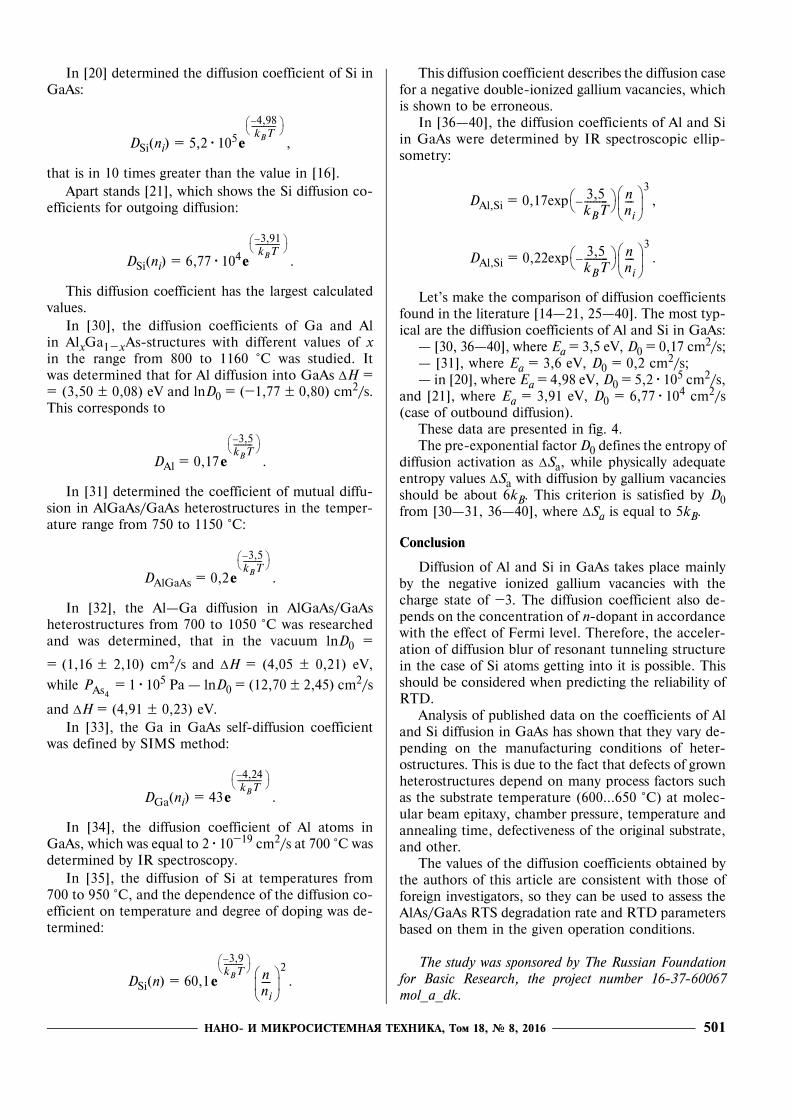
НАНО- И МИКРОСИСТЕМНАЯ ТЕХНИКА, Том 18, № 8, 2016 501
In [20] determined the diffusion coefficient of Si inGaAs:
DSi(ni) = 5,2�105 ,
that is in 10 times greater than the value in [16].Apart stands [21], which shows the Si diffusion co-
efficients for outgoing diffusion:
DSi(ni) = 6,77�104 .
This diffusion coefficient has the largest calculatedvalues.
In [30], the diffusion coefficients of Ga and Alin AlxGa1�xAs-structures with different values of xin the range from 800 to 1160 °C was studied. Itwas determined that for Al diffusion into GaAs ΔH == (3,50 ± 0,08) eV and lnD0 = (�1,77 ± 0,80) cm2/s.This corresponds to
DAl = 0,17 .
In [31] determined the coefficient of mutual diffu-sion in AlGaAs/GaAs heterostructures in the temper-ature range from 750 to 1150 °C:
DAlGaAs = 0,2 .
In [32], the Al�Ga diffusion in AlGaAs/GaAsheterostructures from 700 to 1050 °C was researchedand was determined, that in the vacuum lnD0 =
= (1,16 ± 2,10) cm2/s and ΔH = (4,05 ± 0,21) eV,
while = 1�105 Pa � lnD0 = (12,70 ± 2,45) cm2/s
and ΔH = (4,91 ± 0,23) eV.In [33], the Ga in GaAs self-diffusion coefficient
was defined by SIMS method:
DGa(ni) = 43 .
In [34], the diffusion coefficient of Al atoms inGaAs, which was equal to 2�10�19 cm2/s at 700 °C wasdetermined by IR spectroscopy.
In [35], the diffusion of Si at temperatures from700 to 950 °C, and the dependence of the diffusion co-efficient on temperature and degree of doping was de-termined:
DSi(n) = 60,1 .
This diffusion coefficient describes the diffusion casefor a negative double-ionized gallium vacancies, whichis shown to be erroneous.
In [36�40], the diffusion coefficients of Al and Siin GaAs were determined by IR spectroscopic ellip-sometry:
DAl,Si = 0,17exp ,
DAl,Si = 0,22exp .
Let�s make the comparison of diffusion coefficientsfound in the literature [14�21, 25�40]. The most typ-ical are the diffusion coefficients of Al and Si in GaAs:
� [30, 36�40], where Ea = 3,5 eV, D0 = 0,17 cm2/s;� [31], where Ea = 3,6 eV, D0 = 0,2 cm2/s;� in [20], where Ea = 4,98 eV, D0 = 5,2�105 cm2/s,
and [21], where Ea = 3,91 eV, D0 = 6,77�104 cm2/s(case of outbound diffusion).
These data are presented in fig. 4.The pre-exponential factor D0 defines the entropy of
diffusion activation as ΔSa, while physically adequateentropy values ΔSa with diffusion by gallium vacanciesshould be about 6kB. This criterion is satisfied by D0from [30�31, 36�40], where ΔSa is equal to 5kB.
Conclusion
Diffusion of Al and Si in GaAs takes place mainlyby the negative ionized gallium vacancies with thecharge state of �3. The diffusion coefficient also de-pends on the concentration of n-dopant in accordancewith the effect of Fermi level. Therefore, the acceler-ation of diffusion blur of resonant tunneling structurein the case of Si atoms getting into it is possible. Thisshould be considered when predicting the reliability ofRTD.
Analysis of published data on the coefficients of Aland Si diffusion in GaAs has shown that they vary de-pending on the manufacturing conditions of heter-ostructures. This is due to the fact that defects of grownheterostructures depend on many process factors suchas the substrate temperature (600...650 °C) at molec-ular beam epitaxy, chamber pressure, temperature andannealing time, defectiveness of the original substrate,and other.
The values of the diffusion coefficients obtained bythe authors of this article are consistent with those offoreign investigators, so they can be used to assess theAlAs/GaAs RTS degradation rate and RTD parametersbased on them in the given operation conditions.
The study was sponsored by The Russian Foundationfor Basic Research, the project number 16-37-60067mol_a_dk.
e
4,98–kBT----------⎝ ⎠
⎛ ⎞
e
3,91–kBT----------⎝ ⎠
⎛ ⎞
e
3,5–kBT--------⎝ ⎠
⎛ ⎞
e
3,5–kBT--------⎝ ⎠
⎛ ⎞
PAs4
e
4,24–kBT----------⎝ ⎠
⎛ ⎞
e
3,9–kBT--------⎝ ⎠
⎛ ⎞nni---
⎝ ⎠⎜ ⎟⎛ ⎞ 2
3,5kBT--------–⎝ ⎠
⎛ ⎞ nni---
⎝ ⎠⎜ ⎟⎛ ⎞ 3
3,5kBT--------–⎝ ⎠
⎛ ⎞ nni---
⎝ ⎠⎜ ⎟⎛ ⎞ 3
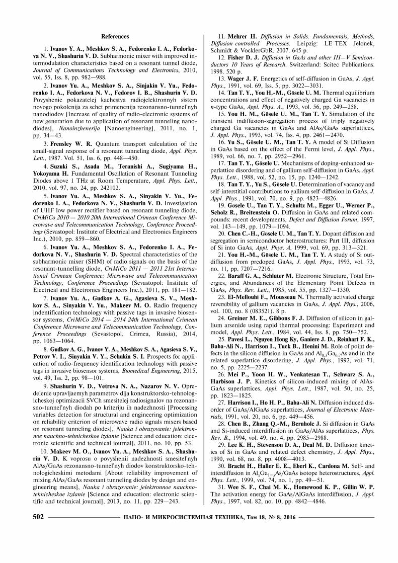
НАНО- И МИКРОСИСТЕМНАЯ ТЕХНИКА, Том 18, № 8, 2016502
References
1. Ivanov Y. A., Meshkov S. A., Fedorenko I. A., Fedorko-va N. V., Shashurin V. D. Subharmonic mixer with improved in-termodulation characteristics based on a resonant tunnel diode,Journal of Communications Technology and Electronics, 2010,vol. 55, Iss. 8, pp. 982�988.
2. Ivanov Yu. A., Meshkov S. A., Sinjakin V. Yu., Fedo-renko I. A., Fedorkova N. V., Fedorov I. B., Shashurin V. D.Povyshenie pokazatelej kachestva radiojelektronnyh sistemnovogo pokolenija za schet primenenija rezonansno-tunnel'nyhnanodiodov [Increase of quality of radio-electronic systems ofnew generation due to application of resonant tunneling nano-diodes], Nanoinzhenerija [Nanoengineering], 2011, no. 1,pp. 34�43.
3. Frensley W. R. Quantum transport calculation of thesmall-signal response of a resonant tunneling diode, Appl. Phys.Lett., 1987. Vol. 51, Iss. 6, pp. 448�450.
4. Suzuki S., Asada M., Teranishi A., Sugiyama H.,Yokoyama H. Fundamental Oscillation of Resonant TunnelingDiodes above 1 THz at Room Temperature, Appl. Phys. Lett.,2010, vol. 97, no. 24, pp. 242102.
5. Ivanov Yu. A., Meshkov S. A., Sinyakin V. Yu., Fe-dorenko I. A., Fedorkova N. V., Shashurin V. D. Investigationof UHF low power rectifier based on resonant tunneling diode,CriMiCo 2010 � 2010 20th International Crimean Conference Mi-crowave and Telecommunication Technology, Conference Proceed-ings (Sevastopol: Institute of Electrical and Electronics EngineersInc.), 2010, pp. 859�860.
6. Ivanov Yu. A., Meshkov S. A., Fedorenko I. A., Fe-dorkova N. V., Shashurin V. D. Spectral characteristics of thesubharmonic mixer (SHM) of radio signals on the basis of theresonant-tunnelling diode, CriMiCo 2011 � 2011 21st Interna-tional Crimean Conference: Microwave and TelecommunicationTechnology, Conference Proceedings (Sevastopol: Institute ofElectrical and Electronics Engineers Inc.), 2011, pp. 181�182.
7. Ivanov Yu. A., Gudkov A. G., Agasieva S. V., Mesh-kov S. A., Sinyakin V. Yu., Makeev M. O. Radio frequencyindentification technology with passive tags in invasive biosen-sor systems, CriMiCo 2014 � 2014 24th International CrimeanConference Microwave and Telecommunication Technology, Con-ference Proceedings (Sevastopol, Crimea, Russia), 2014,pp. 1063�1064.
8. Gudkov A. G., Ivanov Y. A., Meshkov S. A., Agasieva S. V.,Petrov V. I., Sinyakin V. Y., Schukin S. I. Prospects for appli-cation of radio-frequency identification technology with passivetags in invasive biosensor systems, Biomedical Engineering, 2015,vol. 49, Iss. 2, pp. 98�101.
9. Shashurin V. D., Vetrova N. A., Nazarov N. V. Opre-delenie upravljaemyh parametrov dlja konstruktorsko-tehnolog-icheskoj optimizacii SVCh smesitelej radiosignalov na rezonan-sno-tunnel'nyh diodah po kriteriju ih nadezhnosti [Processingvariables detection for structural and engineering optimizationon reliability criterion of microwave radio signals mixers basedon resonant tunneling diodes], Nauka i obrazovanie: jelektron-noe nauchno-tehnicheskoe izdanie [Science and education: elec-tronic scientific and technical journal], 2011, no. 10, pp. 53.
10. Makeev M. O., Ivanov Yu. A., Meshkov S. A., Shashu-rin V. D. K voprosu o povyshenii nadezhnosti smesitel'nyhAlAs/GaAs rezonansno-tunnel'nyh diodov konstruktorsko-teh-nologicheskimi metodami [About reliability improvement ofmixing AlAs/GaAs resonant tunneling diodes by design and en-gineering means], Nauka i obrazovanie: jelektronnoe nauchno-tehnicheskoe izdanie [Science and education: electronic scien-tific and technical journal], 2013, no. 11, pp. 229�243.
11. Mehrer H. Diffusion in Solids. Fundamentals, Methods,Diffusion-controlled Processes. Leipzig: LE-TEX Jelonek,Schmidt & VocklerGbR. 2007. 645 p.
12. Fisher D. J. Diffusion in GaAs and other III�V Semicon-ductors 10 Years of Research. Switzerland: Scitec Publications.1998. 520 p.
13. Wager J. F. Energetics of self-diffusion in GaAs, J. Appl.Phys., 1991, vol. 69, Iss. 5, pp. 3022�3031.
14. Tan T. Y., You H.-M., Gösele U. M. Thermal equilibriumconcentrations and effect of negatively charged Ga vacancies inn-type GaAs, Appl. Phys. A., 1993, vol. 56, pp. 249�258.
15. You H. M., Gösele U. M., Tan T. Y. Simulation of thetransient indiffusion-segregation process of triply negativelycharged Ga vacancies in GaAs and AlAs/GaAs superlattices,J. Appl. Phys., 1993, vol. 74, Iss. 4, pp. 2461�2470.
16. Yu S., Gösele U. M., Tan T. Y. A model of Si Diffusionin GaAs based on the effect of the Fermi level, J. Appl. Phys.,1989, vol. 66, no. 7, pp. 2952�2961.
17. Tan T. Y., Gösele U. Mechanisms of doping-enhanced su-perlattice disordering and of gallium self-diffusion in GaAs, Appl.Phys. Lett., 1988, vol. 52, no. 15, pp. 1240�1242.
18. Tan T. Y., Yu S., Gösele U. Determination of vacancy andself-interstitial contributions to gallium self-diffusion in GaAs, J.Appl. Phys., 1991, vol. 70, no. 9, pp. 4823�4826.
19. Gösele U., Tan T. Y., Schultz M., Egger U., Werner P.,Scholz R., Breitenstein O. Diffusion in GaAs and related com-pounds: recent developments, Defect and Diffusion Forum, 1997,vol. 143�149, pp. 1079�1094.
20. Chen C.-H., Gösele U. M., Tan T. Y. Dopant diffusion andsegregation in semiconductor heterostructures: Part III, diffusionof Si into GaAs, Appl. Phys. A, 1999, vol. 69, pp. 313�321.
21. You H.-M., Gösele U. M., Tan T. Y. A study of Si out-diffusion from predoped GaAs, J. Appl. Phys., 1993, vol. 73,no. 11, pp. 7207�7216.
22. Baraff G. A., Schluter M. Electronic Structure, Total En-ergies, and Abundances of the Elementary Point Defects inGaAs, Phys. Rev. Lett., 1985, vol. 55, pp. 1327�1330.
23. El-Mellouhi F., Mousseau N. Thermally activated chargereversibility of gallium vacancies in GaAs, J. Appl. Phys., 2006,vol. 100, no. 8 (083521). 8 p.
24. Greiner M. E., Gibbons F. J. Diffusion of silicon in gal-lium arsenide using rapid thermal processing: Experiment andmodel, Appl. Phys. Lett., 1984, vol. 44, Iss. 8, pp. 750�752.
25. Pavesi L., Nguyen Hong Ky, Ganiere J. D., Reinhart F. K.,Baba-Ali N., Harrison I., Tuck B., Henini M. Role of point de-fects in the silicon diffusion in GaAs and Al0,3Ga0,7As and in therelated superlattice disordering, J. Appl. Phys., 1992, vol. 71,no. 5, pp. 2225�2237.
26. Mei P., Yoon H. W., Venkatesan T., Schwarz S. A.,Harbison J. P. Kinetics of silicon-induced mixing of AlAs-GaAs superlattices, Appl. Phys. Lett., 1987, vol. 50, no. 25,pp. 1823�1825.
27. Harrison I., Ho H. P., Baba-Ali N. Diffusion induced dis-order of GaAs/AlGaAs superlattices, Journal of Electronic Mate-rials, 1991, vol. 20, no. 6, pp. 449�456.
28. Chen B., Zhang Q.-M., Bernholc J. Si diffusion in GaAsand Si-induced interdiffusion in GaAs/AlAs superlattices, Phys.Rev. B., 1994, vol. 49, no. 4, pp. 2985�2988.
29. Lee K. H., Stevenson D. A., Deal M. D. Diffusion kinet-ics of Si in GaAs and related defect chemistry, J. Appl. Phys.,1990, vol. 68, no. 8, pp. 4008�4013.
30. Bracht H., Haller E. E., Eberl K., Cardona M. Self- andinterdiffusion in AlxGa1�xAs/GaAs isotope heterostructures, Appl.Phys. Lett., 1999, vol. 74, no. 1, pp. 49�51.
31. Wee S. F., Chai M. K., Homewood K. P., Gillin W. P.The activation energy for GaAs/AlGaAs interdiffusion, J. Appl.Phys., 1997, vol. 82, no. 10, pp. 4842�4846.
НАНО- И МИКРОСИСТЕМНАЯ ТЕХНИКА, Том 18, № 8, 2016 503
32. Olmsted B. L., Houde-Walter S. N. Al-Ga interdiffusionthrough group III-vacancy second nearest-neighbor hopping,Appl. Phys. Lett., 1993, vol. 63, no. 4, pp. 530�532.
33. Wang L., Hsu L., Haller E. E., Erickson J. W., Fischer A.,Eberl K., Cardona M. Gaself-diffusion in GaAs isotope hetero-structures, Phys. Rev. Lett., 1996, vol. 76, pp. 2342�2345.
34. Ono H., Ikarashi N., Baba T. Al diffusion into GaAsmonatomic AlAs layers investigated by localized vibrationalmodes, Appl. Phys. Lett., 1995, vol. 66, no. 5, pp. 601�603.
35. Murray J. J., Deal M. D., Allen E. L., Stevenson D. A.,Nozaki S. Modeling Silicon Diffusion in GaAs Using Well De-fined Silicon Doped Molecular Beam Epitaxy Structures, Jour-nal of the Electrochemical Society, 1992, vol. 137, no. 7,pp. 2037�2041.
36. Makeev M. O., Ivanov Yu. A., Meshkov S. A. Issle-dovanie degradacionnyh javlenij v nanorazmernyh AlAs/GaAsgeterostrukturah metodom IK-spektrojellipsometrii [The inves-tigation of degradation phenomena of nanoscale AlAs/GaAs het-erostructures by IR-spectral ellipsometry], Nanoinzhenerija [Na-noengineering], 2011, no. 4, pp. 44�48.
37. Makeev M. O., Ivanov Yu. A., Meshkov S. A., Sinya-kin V. Yu. Investigation of thermal degradation of resonant tunne-ling diodes based on nanoscale AlAs/GaAs heterostructures, Nano-i mikrosistemnaya tekhnika, 2014, no. 2, pp. 23�29.
38. Makeev M. O., Ivanov Yu. A., Sinyakin V. Yu., Mesh-kov S. A., Agasieva S. V., Shashurin V. D. Assessment of resist-ance of AlAs/GaAs nanoscale heterostructures of resonant-tun-neling diodes to diffusion destruction by means of IR-spectro-scopic ellipsometry, CriMiCo 2014 � 2014 24th InternationalCrimean Conference Microwave and Telecommunication Technol-ogy, Conference Proceedings (Sevastopol, Crimea, Russia), 2014,pp. 754�755.
39. Makeev M. O., Ivanov Y. A., Meshkov S. A. Quality di-agnostics of nanoscale AlAs/GaAs resonant tunnelling heter-ostructures based on IR-spectroscopic ellipsometry, J. Phys.:Conf. Ser., 2015, vol. 584, pp. 012014. doi:10.1088/1742-6596/584/1/012014.
40. Makeev M. O., Ivanov Y. A., Meshkov S. A. Assessmentof the resistance to diffusion destruction of AlAs/GaAs nanoscaleresonant-tunneling heterostructures by IR spectral ellipsometry,Semiconductors, 2016, vol. 50, Iss. 1, pp. 83�88.
УДК 621.362
Г. А. Мустафаев, ä-р техн. наук, проф., Д. Г. Мустафаева, канä. техн. наук, äоö., [email protected], М. Г. Мустафаев, канä. техн. наук, ассистентФГБОУ ВО "Северо-Кавказский ãорно-ìетаëëурãи÷еский институт (Госуäарственный техноëоãи÷еский университет)", ã. Вëаäикавказ
ÒÅÕÍÎËÎÃÈ×ÅÑÊÈÅ ÎÑÎÁÅÍÍÎÑÒÈ ÏÎËÓ×ÅÍÈß ÑÎÅÄÈÍÅÍÈÉ ÕÀËÜÊÎÃÅÍÈÄΠÝËÅÌÅÍÒΠÏÅÐÂÎÉ ÃÐÓÏÏÛ È ÒÎÍÊÈÕ ÏËÅÍÎÊÍÀ ÈÕ ÎÑÍÎÂÅ ÇÀÄÀÍÍÎÃÎ ÑÎÑÒÀÂÀ
Введение
Основные параìетры пëено÷ных преобразова-теëей опреäеëяþтся свойстваìи ÷увствитеëüныхэëеìентов, которые, в своþ о÷ереäü, зависят отсвойств ìатериаëов, из которых они изãотовëены.Дëя их изãотовëения испоëüзуþт впоëне опреäе-ëенные ìатериаëы, ÷то связано с ìноãообразиеìи сëожностüþ преäъявëяеìых к ниì требований[1, 2]. Это связано также с техноëоãи÷ескиìи труä-ностяìи, возникаþщиìи в проöессе изãотовëенияпëено÷ных преобразоватеëей [3, 4].
Приìенение соеäинений и спëавов позвоëяетв боëüøей степени обеспе÷итü соответствуþщие
терìоэëектри÷еские параìетры ìатериаëов и реа-ëизоватü усëовия, при которых их соотноøениепривоäит к äостижениþ ìаксиìуìа терìоэëектри-÷еской äобротности. Материаëы äëя преобразова-теëей äоëжны иìетü äостато÷но боëüøуþ терìо-ЭДС, которая äоëжна бытü непрерывной и оäно-зна÷ной функöией теìпературы, ìаксиìаëüнобëизкой к ëинейной; в проöессе экспëуатаöииìатериаëы äоëжны сохранятü своþ терìоэëектри-÷ескуþ характеристику неизìенной.Выбор ìатериаëов äëя эëеìентов пëено÷ных
преобразоватеëей осуществëяþт с у÷етоì их тер-ìоэëектри÷еских свойств, техноëоãии нанесенияпëенки, позвоëяþщей воспроизвоäитü эти свойст-
Поступила в редакцию 10.04.2016 г.
Технологические особенности получения соединений халькогенидов элементов первой группы и тонких пленок задан-ного состава определяются высокой летучестью халькогена, сильной испаряемостью и диссоциацией соединения. Полу-чение соединений заданного состава с хорошими термоэлектрическими свойствами, выбор метода и технологическогорежима нанесения пленки позволяет воспроизводить состав и свойства на пленке.
Ключевые слова: технология, пленка, состав, испарение, диссоциация, режим, температура, преобразователь, ма-териал, свойства
НАНО- И МИКРОСИСТЕМНАЯ ТЕХНИКА, Том 18, № 8, 2016504
ва на пëенке. Материаëаìи с хороøиìи терìо-эëектри÷ескиìи свойстваìи äëя терìоэëектри÷ес-ких устройств и ìикротерìопреобразоватеëей яв-ëяþтся хаëüкоãениäы ìеäи и серебра.Существенное зна÷ение приобретает поëу÷е-
ние соеäинений хаëüкоãениäов эëеìентов первойãруппы заäанноãо состава и пëенок на их основес воспроизвоäиìыìи свойстваìи при изãотов-ëении ÷увствитеëüных эëеìентов преобразовате-ëей [5].
Получение соединений и тонких пленокна их основе заданного состава
Техноëоãия изãотовëения пëено÷ных преобра-зоватеëей состоит из ìножества операöий. Оп-реäеëенная ÷астü операöий преäставëяет собойтонкие и сëожные физико-хиìи÷еские проöессы.Требования высокоãо ка÷ества провеäения техно-ëоãи÷еских операöий обеспе÷иваþтся то÷ностüþпоääержания техноëоãи÷еских режиìов на опти-ìаëüноì уровне и их контроëеì.При созäании пëено÷ных преобразоватеëей к
труäностяì, которые встре÷аþтся при выборе ìа-териаëов с необхоäиìыìи свойстваìи, äобавëя-þтся труäности, связанные с воспроизвеäениеìпараìетров соеäинений исхоäноãо ìатериаëа напëенке. В зависиìости от техноëоãи÷ескоãо режи-ìа нанесения терìоэëектри÷еские свойства поëу-÷енных тонких пëенок сиëüно ìеняþтся и ìоãутзна÷итеëüно отëи÷атüся от свойств испаряеìоãоìатериаëа.Обы÷но неорãани÷еские соеäинения и спëавы
испаряþтся с изìенениеì состава всëеäствие раз-ëи÷ия äавëения паров составëяþщих, поэтоìу со-став пара и конäенсата отëи÷ается от состава ис-хоäноãо ìатериаëа.Техноëоãи÷еские особенности поëу÷ения со-
еäинений хаëüкоãениäов эëеìентов первой ãруп-пы опреäеëяþтся высокой ëету÷естüþ хаëüкоãена,сиëüной испаряеìостüþ и äиссоöиаöией соеäине-ния при теìпературе пëавëения. Всëеäствие ÷еãо,при синтезе исхоäных соеäинений поäъеì теìпе-ратуры происхоäит ìеäëенно, с ÷асовыìи выäерж-каìи при теìпературе на÷аëа реакöии ìежäу ис-хоäныìи коìпонентаìи. Посëе синтеза ãоìоãени-заöия выпоëняется отжиãоì.В терìоäинаìике конäенсированное и ãазооб-
разное состояния вещества характеризуþтся функ-öияìи, которые зависят от äавëения, теìпературы,объеìа и ìассы. При терìоäинаìи÷ескоì равно-весии тверäые теëа характеризуþтся опреäеëен-ныì äавëениеì паров, которое зависит тоëüко оттеìпературы.Давëение насыщенноãо пара наä поверхностüþ
конäенсированной фазы явëяется важной веëи÷и-
ной, позвоëяþщей оöенитü способностü веществак испарениþ и те теìпературы, при которых äо-стижиìы необхоäиìые скорости испарения. Осо-бое зна÷ение оно приобретает äëя соеäинений.Равновесное äавëение опреäеëяется свобоäнойэнерãией испарения при äанной теìпературе.Испарение соеäинений сопровожäается äиссо-
öиаöией. Диссоöиаöия обы÷но сиëüно вëияет настехиоìетри÷еское соотноøение составëяþщих,÷то особенно проявëяется, есëи оäин из проäуктовäиссоöиаöии явëяется неëету÷иì.Дëя бинарных соеäинений ÷асто набëþäается
испарение с äиссоöиаöией, к такиì соеäиненияìотносятся хаëüкоãениäы серебра.Оäинаковая ëету÷естü обеих составëяþщих
соеäинений явëяется необхоäиìыì, но неäоста-то÷ныì усëовиеì осажäения пëенок исхоäноãосостава.Некоторые соеäинения испаряþтся несоãëасо-
ванно, т.е. при повыøенных теìпературах ëету-÷естü их составëяþщих отëи÷ается стоëü сиëüно,÷то хиìи÷еский состав пара и пëенки не совпа-äает с хиìи÷ескиì составоì испаряеìоãо вещес-тва. К такиì соеäиненияì относятся хаëüкоãени-äы ìеäи.При изãотовëении пëено÷ных преобразоватеëей
существенное зна÷ение иìеет техноëоãия поëу÷е-ния тонких пëенок соеäинений заäанноãо состава,так как поëу÷ение пëенок соеäинений исхоäноãосостава связано со зна÷итеëüныìи техноëоãи÷ес-киìи труäностяìи. Это связано в первуþ о÷ереäü стеì, ÷то усëовия осажäения сиëüно вëияþт на со-став пëенок. Пëенки ìноãокоìпонентных ìате-риаëов труäно воспроизвоäиìы по составу. Труä-ности поëу÷ения пëенок связаны с теì, ÷то прииспарении происхоäит разäеëение соеäинения наотäеëüные коìпоненты, испаряþщиеся с разëи÷-ныìи скоростяìи.Провеäенный анаëиз показывает на поëожи-
теëüное вëияние увеëи÷ения скорости испарения иосажäения на поëу÷ение оäнороäных пëенок хаëü-коãениäов ìеäи и серебра заäанноãо состава исвойств. При этоì вещество перехоäит в ãазооб-разное состояние без изìенения виäа ìоëекуëы,÷то позвоëяет поëу÷атü пëенки такоãо же состава,как и состав исхоäноãо ìатериаëа.Выбор ìетоäа поëу÷ения тонких пëенок зави-
сит от назна÷ения тонкой пëенки, совìестиìостиìетоäа с äруãиìи техноëоãи÷ескиìи операöияìиìикроэëектронной техноëоãии. Дëя обеспе÷ениявоспроизвоäиìости эëектрофизи÷еских свойствтонких пëенок ìетоäы осажäения äоëжны позво-ëятü поëу÷атü пëенки исхоäноãо состава.Дëя поëу÷ения пëенок хаëüкоãениäов ìеäи и
серебра исхоäноãо состава приìенен ìетоä äиск-ретноãо испарения в вакууìе. Вещество испаря-
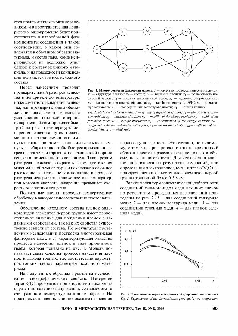
НАНО- И МИКРОСИСТЕМНАЯ ТЕХНИКА, Том 18, № 8, 2016 505
ется практи÷ески ìãновенно и öе-ëикоì, и в пространстве наä испа-ритеëеì оäновреìенно буäут при-сутствоватü в парообразной фазекоìпоненты соеäинения в такоìсоотноøении, в какоì они со-äержатся в объеìноì образöе ìа-териаëа, и состав пара, конäенси-руþщеãося на поäëожке, буäетбëизок к составу исхоäноãо ìате-риаëа, и на поверхности конäенса-öии поëу÷ается пëенка исхоäноãосостава.Переä нанесениеì провоäят
преäваритеëüный разоãрев вещес-тва в испаритеëе äо теìпературыниже заìетноãо испарения вещес-тва, äëя преäваритеëüноãо обезãа-живания испаряеìоãо вещества иуìенüøения тепëовой инерöиииспаритеëя. Затеì провоäят быс-трый наãрев äо теìпературы ис-парения вещества путеì поäа÷иìощноãо кратковреìенноãо иì-пуëüса тока. При этоì зна÷ение и äëитеëüностü иì-пуëüса выбираþт так, ÷тобы быстрее произоøëи на-ãрев испаритеëя и взрывное испарение всей порöиивещества, поìещенноãо в испаритеëü. Такой режиìразоãрева позвоëяет сократитü вреìя äостиженияìаксиìаëüной теìпературы и искëþ÷ает возìожноерассëоение вещества по коìпонентаì в проöессеразоãрева испаритеëя, а также äости÷ü теìператур,при которых скоростü испарения превыøает ско-ростü разëожения вещества.Поëу÷енные пëенки прохоäят теìпературнуþ
обработку в вакууìе непосреäственно посëе напы-ëения.Обеспе÷ение исхоäноãо состава пëенок хаëü-
коãениäов эëеìентов первой ãруппы иìеет перво-степенное зна÷ение äëя поëу÷ения пëенок с за-äанныìи свойстваìи, так как их свойства сущес-твенно зависят от состава. По резуëüтатаì прове-äенных иссëеäований построена ìноãоуровневаяфакторная ìоäеëü F, характеризуþщая ка÷ествопроöесса нанесения пëенок в виäе при÷инноãоãрафа, которая показана на рис. 1. Моäеëü по-казывает связü ка÷ества проöесса нанесения пëе-нок и выхоäа ãоäных, т.е. соответствие параìет-ров тонких пëенок параìетраì исхоäноãо ìате-риаëа.На поëу÷енных образöах провеäены иссëеäо-
вания эëектрофизи÷еских свойств. ИзìерениетерìоЭДС провоäится при отсутствии тока ÷ерезобразеö по паäениþ напряжения, созäаваеìоãо зас÷ет разности теìператур на конöах образöа. Напровоäиìостü пëенок вëияние оказываþт явëения
переноса у поверхности. Это связано, по-виäиìо-ìу, с теì, ÷то при протекании тока ÷ерез тонкийобразеö носитеëи рассеиваþтся не тоëüко в объ-еìе, но и на поверхности. Дëя искëþ÷ения вëия-ния поверхности на резуëüтаты изìерений, приопреäеëении эëектропровоäности и терìоЭДС ис-поëüзуþт пëенки хаëüкоãениäов эëеìентов первойãруппы тоëщиной боëее 0,3 ìкì.Зависиìости терìоэëектри÷еской äобротности
соеäинений хаëüкоãениäов ìеäи и тонких пëенокпо резуëüтатаì провеäенных иссëеäований при-веäены на рис. 2 (1 � äëя соеäинений теëëуриäаìеäи; 2 � äëя пëенок теëëуриäа ìеäи; 3 � äëясоеäинений сеëениäа ìеäи; 4 � äëя пëенок сеëе-ниäа ìеäи).
Рис. 2. Зависимости термоэлектрической добротности от составаFig. 2. Dependences of the thermoelectric good quality on composition
Рис. 1. Многоуровневая факторная модель: F � ка÷ество проöесса нанесения пëенок;x1 � структура пëенки; x2 � состав; x3 � тоëщина пëенки; x4 � поäвижностü но-ситеëей заряäа; x5 � øирина запрещенной зоны; x6 � уäеëüное сопротивëение;x7 � конöентраöия носитеëей заряäа; x8 � коэффиöиент терìоЭДС; x9 � эëектро-провоäиìостü; x10 � коэффиöиент тепëопровоäности; x11 � выхоä ãоäных
Fig. 1. Multilevel factorial model: F � quality of deposition of films; x1 � film structure; x2 �composition; x3 � thickness of a film; x4 � mobility of the charge carriers; x5 � width of theforbidden zone; x6 � specific resistance; x7 � concentration of the charge carriers; x8 �coefficient of the thermal electromotive force; x9 � electroconductivity; x10 � coefficient of heatconductivity; x11 � yield ratio
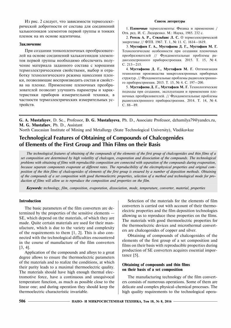
НАНО- И МИКРОСИСТЕМНАЯ ТЕХНИКА, Том 18, № 8, 2016506
Из рис. 2 сëеäует, ÷то зависиìости терìоэëект-ри÷еской äобротности от состава äëя соеäиненийхаëüкоãениäов эëеìентов первой ãруппы и тонкихпëенок на их основе иäенти÷ны.
Заключение
При созäании тонкопëено÷ных преобразовате-ëей на основе соеäинений хаëüкоãениäов эëеìен-тов первой ãруппы необхоäиìо обеспе÷итü поëу-÷ение ìатериаëа заäанноãо состава с хороøиìитерìоэëектри÷ескиìи свойстваìи, выбор и отра-ботку техноëоãи÷ескоãо режиìа нанесения пëен-ки, позвоëяþщие воспроизвоäитü состав и свойст-ва на пëенке. Приìенение пëено÷ных преобра-зоватеëей позвоëит уëу÷øитü параìетры и харак-теристики приборов изìеритеëüной техники, в÷астности терìоэëектри÷еских изìеритеëüных ус-тройств.
Список литературы
1. Пленочные терìоэëеìенты: Физика и приìенение /Отв. реä. И. С. Лиäоренко. М.: Наука, 1985. 232 с.
2. Регель А. Р., Стильбанс Л. С. О терìоэëектри÷ескойэнерãетике // ФТП. 1967. Т. 1, № 11. С. 1614�1619.
3. Мустафаев Г. А., Мустафаева Д. Г., Мустафаев М. Г.Техноëоãи÷еские особенности при созäании пëено÷ныхпреобразоватеëей // Фунäаìентаëüные пробëеìы ра-äиоэëектронноãо приборостроения. 2015. Т. 15, № 4.С. 213�215.
4. Мустафаева Д. Г., Мустафаев М. Г. Оптиìизаöиятехноëоãии произвоäства ìикроэëектронных приборныхструктур. // Фунäаìентаëüные пробëеìы раäиоэëектронно-ãо приборостроения. 2015. Т. 15, № 4. С. 197�200.
5. Мустафаева Д. Г., Мустафаев М. Г. Техноëоãи÷ескиепоäхоäы при созäании, экспëуатаöии и приìенении пëе-но÷ных преобразоватеëей. // Фунäаìентаëüные пробëеìыраäиоэëектронноãо приборостроения. 2014. Т. 14, № 4.С. 88�89.
G. A. Mustafayev, D. Sc., Professor, D. G. Mustafayeva, Ph. D., Associate Professor, [email protected], M. G. Mustafaev, Ph. D., AssistantNorth Caucasian Institute of Mining and Metallurgy (State Technological University), Vladikavkaz
Technological Features of Obtaining of Compounds of Chalcogenides of Elements of the First Group and Thin Films on their Basis
Introduction
The basic parameters of the film converters are de-termined by the properties of the sensitive elements �SE, which depend on the materials, of which they aremade. Quite certain materials are used for their man-ufacture, which is due to the variety and complexityof the requirements to them [1, 2]. This is also con-nected with the technological difficulties encounteredin the course of manufacture of the film converters[3, 4].
Application of the compounds and alloys to a greatdegree allows to ensure the thermoelectric parametersof the materials and to realize the conditions, at whichtheir parity leads to a maximal thermoelectric quality.The materials should have high enough thermal elec-tromotive force, have a continuous and unequivocaltemperature function, as much as possible close to thelinear one; and during operation they should keep thethermoelectric characteristic invariable.
Selection of the materials for the elements of filmconverters is carried out with account of their thermo-electric properties and the film deposition technologiesallowing us to reproduce these properties on the films.The materials with good thermoelectric properties forthe thermoelectric devices and microthermal convert-ers are chalcogenides of copper and silver.
Obtaining of compounds of chalcogenides of theelements of the first group of a set composition andfilms on their basis with reproducible properties duringproduction of SE converters acquires essential impor-tance [5].
Obtaining of compounds and thin filmson their basis of a set composition
The manufacturing technology of the film convert-ers consists of numerous operations. Some of them aredelicate and complex physical-chemical processes. Thehigh quality requirements to the technological opera-
The technological features of obtaining of the compounds of the elements of the first group of chalcogenides and thin films of aset composition are determined by high volatility of chalcogen, evaporation and dissociation of the compounds. The technologicalproblems with obtaining of films with reproducible composition are connected with separation of the compounds during evaporation,because separate components evaporate at different rates. The reproducibility of the electrophysical properties and original com-position of the thin films of chalcogenides of elements of the first group is ensured by a number of deposition methods. Obtainingof the compounds of a set composition with good thermoelectric properties, selection of a method and technological mode for pro-duction of films will allow us to reproduce the composition and properties on the film.
Keywords: technology, film, composition, evaporation, dissociation, mode, temperature, converter, material, properties
НАНО- И МИКРОСИСТЕМНАЯ ТЕХНИКА, Том 18, № 8, 2016 507
tions are ensured by the accuracy of maintaining of thetechnological modes at the optimal level and controlover them.
Creation of the film converters encounters not on-ly the difficulties with selection of the materials withthe necessary properties, but also the problems con-nected with reproduction of the parameters of thecompounds of the initial material on the films. De-pending on a deposition mode, the thermoelectricproperties of the received thin films vary greatly andcan differ considerably from the properties of theevaporated material.
Usually, the inorganic compounds and alloys evap-orate alongside with a change of the composition owingto different vapor pressures of the components, there-fore, the compositions of the vapor and of the conden-sate differ from that of the initial material.
The technological features of obtaining of com-pounds of chalcogenides of the elements of the firstgroup are determined by their high volatility, vapora-bility and dissociation at the melting temperature. Ow-ing to that, during synthesis of the initial compoundsthe temperature is raised slowly, with hour soakings atthe temperature of the beginning of the reaction be-tween the initial components. After the synthesis, thehomogenization is carried out by annealing.
During production of the film converters, dependingon a deposition mode, the thermoelectric properties ofthe received thin films vary greatly and can differ con-siderably from the properties of the evaporated material.
In thermodynamics the condensed and gaseousstates of a substance are characterized by the functions,which depend on pressure, temperatures, volume andweight. In case of a thermodynamic balance the solidbodies are characterized by a certain pressure of vapors,which depends only on the temperature.
The pressure of the saturated vapor over the surfaceof the condensed phase is an important value allowingto estimate the evaporation ability of a substance andthe temperatures, at which the necessary speeds ofevaporation are achievable. It acquires special impor-tance for the compounds. An equilibrium pressure isdetermined by the free energy of evaporation at the giv-en temperature.
Evaporation is accompanied by dissociation of thecompounds. Usually, the dissociation has a strong in-fluence on the stoichiometric correlation of the com-ponents, which is especially pronounced, if one of theproducts of the dissociation is nonvolatile.
For binary compounds the evaporation is often ob-served with dissociation. Among such compounds arechalcogenides of silver.
Identical volatility of both components of the com-pounds is a necessary, but not a sufficient condition fordeposition of films of the initial composition.
Some compounds evaporate discordantly, i.e. athigher temperatures the volatility of their componentsdiffers so radically, that the chemical composition ofthe vapor and of the film does not coincide with thechemical composition of the evaporated substance. Tosuch compounds belong the chalcogenides of copper.
In manufacture of the film converters an importantrole is played by the technology for reception of thin filmsof the compounds of the set composition, because this isconnected with considerable technological difficulties,explained, first of all, by the fact that the deposition con-ditions have a strong influence on the composition offilms. Composition of films of the multicomponent ma-terials is difficult to reproduce. The problems with recep-tion of the films are due to the fact that the evaporationcauses partitioning of a compound into separate compo-nents evaporating with various speeds.
Analysis demonstrates a positive influence of an in-crease of the speed of evaporation and deposition onthe reception of the homogeneous films of chalcoge-nides of copper and silver of the set composition andproperties. At that, a substance turns into a gaseousstate without changing the kind of its molecules, whichallows us to receive films of the same composition asthat of the initial material.
Selection of a method for obtaining of the films de-pends on the purpose of a thin film, and compatibilityof a method with the other technological operations ofthe microelectronic technology. In order to ensure re-producibility of the electrophysical properties of thethin films, the deposition methods should allow us toreceive films of the initial composition.
For reception of the films of chalcogenides of cop-per and silver of the initial composition, the methodof a discrete evaporation in vacuum is applied. A sub-stance evaporates practically instantly and entirely,and at the vaporous phase in the space over the evap-orator there will be components of compounds in sucha correlation, in which they are in the volume sampleof a material, and the composition of the vapor con-densed on a substrate will be close to the compositionof the initial material, and the film of the initial com-position will appear on the condensation surface.
Before a deposition, a substance is heated up in theevaporator up to the temperature below an appreciableevaporation of the substance, for a preliminary degas-sing of the evaporated substance and reduction of thethermal inertia of the evaporator. Then, fast heating isdone up to the temperature of evaporation of the sub-stance by giving a powerful momentary impulse of acurrent. At that, the parameters of such an impulse areselected, which can ensure the most rapid heating of theevaporator and an explosive evaporation of all the sub-stance placed in the evaporator. This heating reducesthe time of achievement of the maximal temperature,excludes a possible stratification of the substance in the
НАНО- И МИКРОСИСТЕМНАЯ ТЕХНИКА, Том 18, № 8, 2016508
components during heating of the evaporator, andhelps to reach the temperatures, at which the speed ofthe evaporation exceeds the speed of the decompositionof the substance.
The received films undergo the temperatureprocessing in vacuum directly after deposition.
Preserving of the initial composition of the films ofchalcogenides of elements of the first group has a par-amount value for reception of the films with the setproperties, because their properties essentially dependon the composition. By the results of the research amultilevel factorial model F was constructed character-izing the quality of the deposition process of the filmsin the form of a causal graph (fig. 1). The model showsa connection between the quality of the films and theyield ratio, i.e. correspondence of the parameters of thethin films to the parameters of the initial material.
On the samples a research was done of their elec-trophysical properties. Measurement of the thermalelectromotive force was done in the absence of a cur-rent through the sample by a voltage drop, created dueto the difference of temperatures on the ends of thesample. Conductivity of the films is influenced by thetransfer near the surface. This is connected with the factthat, when the current goes through a thin sample thecarriers dissipate not only in the volume, but also on thesurface. In order to exclude the influence of the surfaceon the results of measurements, during determinationof electroconductivity and thermal electromotive force,the films of chalcogenides are used with thickness morethan 0,3 micrometers.
Dependences of the thermoelectric good quality ofthe compounds of chalcogenides of copper and thinfilms by the results of the research are presented in fig. 2(1 � for copper telluride; 2 � for the films of copper
telluride; 3 � for copper selenide; 4 � for the films ofcopper selenide).
From fig. 2 it follows, that the dependences of thethermoelectric good quality on the composition for thecompounds of chalcogenides of elements of the firstgroup and thin films on their basis are identical.
Conclusion
During creation of the thin-film converters on thebasis of the compounds of chalcogenides of the ele-ments of the first group it is necessary to ensure obtain-ing of a material of a set composition with good ther-moelectric properties, selection and development of atechnological mode of deposition of films, allowing usto reproduce the composition and properties on a film.Application of the film converters will allow us to im-prove the parameters and characteristics of the meas-uring devices, of the thermoelectric measuring devices,in particular.
References
1. Plenochnye termojelementy: Fizika i primenenie, Otv. red. I.S. Lidorenko, Moscow, Nauka, 1985, 232 p.
2. Regel' A. R., Stil'bans L. S. O termojelektricheskoj jen-ergetike, FTP, 1967, vol. 1, no. 11, pp. 1614�1619.
3. Mustafaev G. A., Mustafaeva D. G., Mustafaev M. G.Tehnologicheskie osobennosti pri sozdanii plenochnyh preobra-zovatelej, Fundamental'nye problemy radiojelektronnogo priboros-troenija, 2015, vol. 15, no. 4, 4, pp. 213�215.
4. Mustafaeva D. G., Mustafaev M. G. Optimizacija teh-nologii proizvodstva mikrojelektronnyh pribornyh struktur, Fun-damental'nye problemy radiojelektronnogo priborostroenija, 2015,vol. 15, no. 4, p. 197�200.
5. Mustafaeva D. G., Mustafaev M. G. Tehnologicheskiepodhody pri sozdanii, jekspluatacii i primenenii plenochnyh pre-obrazovatelej. // Fundamental'nye problemy radiojelektronnogopriborostroenija, 2014, vol. 14, no. 4, pp. 88�89.
Íîâàÿ êíèãàÈ. È. Àáðàìîâ. Îñíîâû ìîäåëèðîâàíèÿ ýëåìåíòîâ ìèêðî- è íàíîýëåêòðîíèêè.LAP LAMBERT Academic Publishing, Germany, 2016. 444 ñ.
В ìоноãрафии рассìотрены физи÷еские основы, пробëеìы и принöипы ìоäеëирования приборныхструктур (эëеìентов) ìикро- и наноэëектроники. С еäиных позиöий провеäена систеìатизаöия ìоäеëейэëеìентов. Основное вниìание уäеëено наибоëее аäекватныì ÷исëенныì ìоäеëяì. Книãа преäназна÷енаäëя спеöиаëистов в обëасти ìикро- и наноэëектроники, препоäаватеëяì, аспирантаì, ìаãистрантаì и сту-äентаì соответствуþщих спеöиаëüностей. Моноãрафия написана на основе статей автора, опубëикован-ных в веäущих нау÷но-техни÷еских журнаëах Российской Феäераöии в обëасти ìикро- и наноэëектро-ники, и обобщает еãо сорокаëетний опыт работы в äанной обëасти науки.
Инфорìаöиþ о книãе и ее приобретение ìожно осуществитü, обративøисü на сайт:https://www.ljubljuknigi.ru/
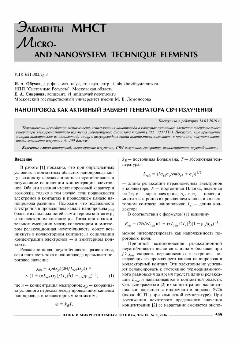
НАНО- И МИКРОСИСТЕМНАЯ ТЕХНИКА, Том 18, № 8, 2016 509
УДК 621.382.2/.3
И. А. Обухов, ä-р физ.-ìат. наук, ст. нау÷. сотр., [email protected]НПП "Систеìные Ресурсы", Московская обëастü, Е. А. Смирнова, аспирант, [email protected] Московский ãосуäарственный университет иìени М. В. Лоìоносова
ÍÀÍÎÏÐÎÂÎÄ ÊÀÊ ÀÊÒÈÂÍÛÉ ÝËÅÌÅÍÒ ÃÅÍÅÐÀÒÎÐÀ ÑÂ× ÈÇËÓ×ÅÍÈß
Введение
В работе [1] показано, ÷то при опреäеëенныхусëовиях в контактных обëастях нанопровоäа ìо-ãут возникнутü реëаксаöионная неустой÷ивостü изатухаþщие осöиëëяöии конöентраöии эëектро-нов. Оба эти явëения иìеþт пороãовый характер ивозìожны тоëüко в тоì сëу÷ае, есëи поäвижностиэëектронов в контактах и провоäящеì канаëе на-нопровоäа разëи÷ны. Поëожиì, ÷то поäвижностüэëектронов в провоäящеì канаëе нанопровоäа μchбоëüøе их поäвижностей в эìиттерноì контакте μeи коëëекторноì контакте μc. Тоãäа при поëожи-теëüноì сìещении ìежäу коëëектороì и эìитте-роì реëаксаöионная неустой÷ивостü ìожет воз-никнутü в коëëекторноì контакте, а осöиëëяöииконöентраöии эëектронов � в эìиттерноì кон-такте.Реëаксаöионная неустой÷ивостü развивается,
есëи пëотностü тока в нанопровоäе превыøает по-роãовое зна÷ение
jins = μcn(xjc)(2Θ/Lrelc(xjc)) Ѕ
Ѕ (1 + (πLrelc(xjc)/2Lc)2(1 � μc/μch)
�1, (1)
ãäе n � конöентраöия эëектронов; xjc � коорäина-та усëовноãо перехоäа ìежäу провоäящиì канаëоìнанопровоäа и коëëекторныì контактоì;
Θ = kBT,
kB � постоянная Боëüöìана, T � абсоëþтная теì-пература;
Lrelc = ($σchσc/en(σch + σc))1/2
� äëина реëаксаöии неравновесных эëектроновв коëëекторе; $ � постоянная Пëанка, äеëеннаяна 2π; e � заряä эëектрона; σch и σc � провоäи-ìости эëектронов в провоäящеì канаëе и коëëек-торноì контакте нанопровоäа; Lc � äëина коë-ëектора.В соответствии с форìуëой (1) веëи÷ину
Eins = (2Θ/eLrelc)(1 + (πLrelc/2Lc)2)(1 � μc/μch)
�1,
ìожно интерпретироватü как напряженностü по-роãовоãо поëя.При÷иной возникновения реëаксаöионной
неустой÷ивости явëяется сëиøкоì боëüøая приj > jins скоростü неравновесных эëектронов, по-паäаþщих из провоäящеãо канаëа нанопровоäа вкоëëекторный контакт. Эти эëектроны не успева-þт реëаксироватü к состояниþ терìоäинаìи÷ес-коãо равновесия за вреìя проëета äëины реëакса-öии Lrelc и накапëиваþтся в контактной обëасти.Соãëасно рас÷етаì [2] их конöентраöия экспонен-öиаëüно нарастает с инкреìентоì поряäка Θ/2h(окоëо 40 ТГö при коìнатной теìпературе). Приäостижении некотороãо преäеëüноãо зна÷енияконöентраöии [2] ее нарастание сìеняется экспо-
Поступила в редакцию 14.03.2016 г.
Теоретически исследована возможность использования нанопровода в качестве активного элемента твердотельногогенератора электромагнитного излучения терагерцевого диапазона частот (300...3000 ГГц). Показано, что применениематриц нанопроводов из антимонида индия с полупроводниковыми контактами позволяет, в принципе, получить плот-ность мощности излучения до 100 Вт/см2.
Ключевые слова: нанопровод, терагерцевое излучение, СВЧ излучение, генератор, релаксационная неустойчивость
ÝËÅÌÅÍÒÛ ÌÍÑÒMICRO-
AND NANOSYSTEM TECHNIQUE ELEMENTS
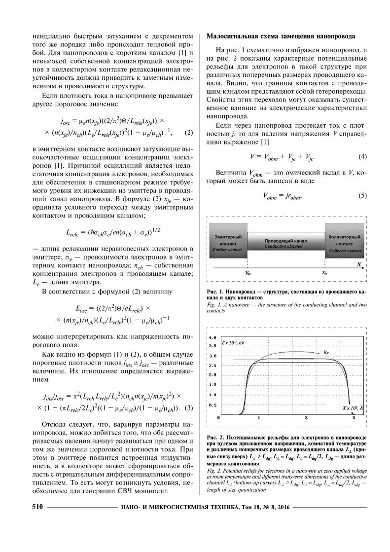
НАНО- И МИКРОСИСТЕМНАЯ ТЕХНИКА, Том 18, № 8, 2016510
ненöиаëüно быстрыì затуханиеì с äекреìентоìтоãо же поряäка ëибо происхоäит тепëовой про-бой. Дëя нанопровоäов с короткиì канаëоì [1] иневысокой собственной конöентраöией эëектро-нов в коëëекторноì контакте реëаксаöионная не-устой÷ивостü äоëжна привоäитü к заìетныì изìе-ненияì в провоäиìости структуры.
Есëи пëотностü тока в нанопровоäе превыøаетäруãое пороãовое зна÷ение
josc = μen(xje)((2/π2)Θ/Lrele(xje)) Ѕ
Ѕ (n(xje)/nch)(Le/Lrele(xje))2(1 � μe/μch)
�1, (2)
в эìиттерноì контакте возникаþт затухаþщие вы-соко÷астотные осöиëëяöии конöентраöии эëект-ронов [1]. При÷иной осöиëëяöий явëяется неäо-стато÷ная конöентраöия эëектронов, необхоäиìыхäëя обеспе÷ения в стаöионарноì режиìе требуе-ìоãо уровня их инжекöии из эìиттера в провоäя-щий канаë нанопровоäа. В форìуëе (2) xje � ко-орäината усëовноãо перехоäа ìежäу эìиттерныìконтактоì и провоäящиì канаëоì;
Lrele = ($σchσe/en(σch + σe))1/2
� äëина реëаксаöии неравновесных эëектронов вэìиттере; σe � провоäиìости эëектронов в эìит-терноì контакте нанопровоäа; nch � собственнаяконöентраöия эëектронов в провоäящеì канаëе;Le � äëина эìиттера.
В соответствии с форìуëой (2) веëи÷ину
Eosc = ((2/π2)Θ/eLrele) Ѕ
Ѕ (n(xje)/nch)(Le/Lrele)2(1 � μe/μch)
�1
ìожно интерпретироватü как напряженностü по-роãовоãо поëя.
Как виäно из форìуë (1) и (2), в общеì сëу÷аепороãовые пëотности токов jins и josc � разëи÷ныевеëи÷ины. Их отноøение опреäеëяется выраже-ниеì
jins/josc = π2(LrelcLrele/Le2)(nchn(xjc)/n(xje)
2) Ѕ
Ѕ (1 + (πLrelc/2Lc)2((1 � μe/μch)/(1 � μc/μch)). (3)
Отсþäа сëеäует, ÷то, варüируя параìетры на-нопровоäа, ìожно äобитüся тоãо, ÷то оба рассìат-риваеìых явëения на÷нут развиватüся при оäноì итоì же зна÷ении пороãовой пëотности тока. Приэтоì в эìиттере появится встроенная инäуктив-ностü, а в коëëекторе ìожет сфорìироватüся об-ëастü с отриöатеëüныì äифференöиаëüныì сопро-тивëениеì. То естü ìоãут возникнутü усëовия, не-обхоäиìые äëя ãенераöии СВЧ ìощности.
Малосигнальная схема замещения нанопровода
На рис. 1 схеìати÷но изображен нанопровоä, ана рис. 2 показаны характерные потенöиаëüныереëüефы äëя эëектронов в такой структуре приразëи÷ных попере÷ных разìерах провоäящеãо ка-наëа. Виäно, ÷то ãраниöы контактов с провоäя-щиì канаëоì преäставëяþт собой ãетероперехоäы.Свойства этих перехоäов ìоãут оказыватü сущест-венное вëияние на эëектри÷еские характеристикинанопровоäа.Есëи ÷ерез нанопровоä протекает ток с пëот-
ностüþ j, то äëя паäения напряжения V справеä-ëиво выражение [1]
V = Vohm + Vje + Vjc. (4)
Веëи÷ина Vohm � это оìи÷еский вкëаä в V, ко-торый ìожет бытü записан в виäе
Vohm = jrohm, (5)
Рис. 1. Нанопровод � структура, состоящая из проводящего ка-нала и двух контактовFig. 1. A nanowire � the structure of the conducting channel and twocontacts
Рис. 2. Потенциальные рельефы для электронов в нанопроводепри нулевом приложенном напряжении, комнатной температуреи различных поперечных размерах проводящего канала L^ (кри-вые снизу вверх) L^ > Ldq, L^ = Ldq, L^ = Ldq/2, Ldq � длина раз-мерного квантованияFig. 2. Potential reliefs for electrons in a nanowire at zero applied voltageat room temperature and different transverse dimensions of the conductivechannel L⊥ (bottom-up curves) L⊥ > Ldq, L⊥ = Ldq, L⊥ = Ldq/2, Ldq �length of size quantization
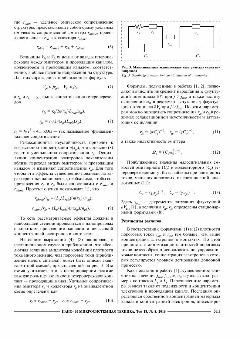
НАНО- И МИКРОСИСТЕМНАЯ ТЕХНИКА, Том 18, № 8, 2016 511
ãäе rohm � уäеëüное оìи÷еское сопротивëениеструктуры, преäставëяþщее собой суììу уäеëüныхоìи÷еских сопротивëений эìиттера rohme, прово-äящеãо канаëа rch и коëëектора rohmc:
rohm = rohme + rch + rohmc. (6)
Веëи÷ины Vje и Vjc описываþт вкëаäы ãетеропе-рехоäов ìежäу эìиттероì и провоäящиì канаëоì,коëëектороì и провоäящиì канаëоì, соответст-венно, в общее паäение напряжения на структуре.Дëя них справеäëивы прибëиженные форìуëы
Vje ≈ jrje, Vjc ≈ jrjc, (7)
а rje и rjc � уäеëüные сопротивëения ãетероперехо-äов
rje = r0/2n(xje)Lrele(xje),
rjc = r0/2n(xjc)Lrelc(xjc); (8)
r0 = $/e2 ≈ 4,1 кОì � так называеìое "фунäаìен-таëüное сопротивëение".
Реëаксаöионная неустой÷ивостü привоäит квозрастаниþ конöентраöии n(xjc), ÷то соãëасно (8)веäет к уìенüøениþ сопротивëения rjc. Осöиë-ëяöии конöентраöии эëектронов ëокаëизованывбëизи перехоäа ìежäу эìиттероì и провоäящиìканаëоì и изìеняþт сопротивëение rje. Дëя тоãо÷тобы эти эффекты существенно повëияëи на ха-рактеристики нанопровоäа, необхоäиìо, ÷тобы со-противëения rjc и rje быëи сопоставиìы с rohmc иrohme. Простые оöенки показываþт [1], ÷то
rohmc/rjc ∼ (Lc/Lrelc)(n(xjc)/nch),
rohme/rje ∼ (Le/Lrele)(n(xje)/nch). (9)
То естü рассìатриваеìые эффекты äоëжны внаибоëüøей степени проявëятüся в нанопровоäахс короткиì провоäящиì канаëоì и невысокойконöентраöией эëектронов в контактах.
На основе выражений (4)�(8) нанопровоä внестаöионарноì сëу÷ае в прибëижении, ÷то абсо-ëþтная веëи÷ина аìпëитуäы коëебаний пëотноститока ìноãо ìенüøе, ÷еì пороãовые токи (прибëи-жение ìаëоãо сиãнаëа), ìожет бытü описан экви-ваëентной схеìой, преäставëенной на рис. 3. Этасхеìа у÷итывает, ÷то в нестаöионарноì режиìеважнуþ роëü иãраþт еìкости ãетероперехоäов кон-такт � провоäящий канаë. Уäеëüные сопротивëе-ния эìиттера re и коëëектора rc на эквиваëентнойсхеìе опреäеëены как
re ≈ rohme + rje, rc ≈ rohmc + rjc. (10)
Форìуëы, поëу÷енные в работах [1, 2], позво-ëяþт вы÷исëитü инкреìент нарастания æ фëукту-аöий потенöиаëа δVc при j > jins, а также ÷астотуосöиëëяöий ω0 и äекреìент затухания γ фëуктуа-öий потенöиаëа δVe при j > josc. По этиì параìет-раì ìожно опреäеëитü сопротивëения rjc и rje в ре-жиìах реëаксаöионной неустой÷ивости и затуха-þщих осöиëëяöий
rjc = (æCc)�1, rje = (γCe)
�1, (11)
а также инäуктивностü эìиттера
Le = (Ce )�1. (12)
Прибëиженные зна÷ения ìаëосиãнаëüных еì-костей эìиттерноãо (Ce) и коëëекторноãо (Cc) ãе-тероперехоäов ìоãут бытü найäены при пëотностяхтоков, ìенüøих пороãовых, из соотноøений, ана-ëоãи÷ных (11):
Ce = (γerje)�1, Cc = (γcrjc)
�1. (13)
Зäесü γe,c � äекреìенты затухания фëуктуаöийδVe,c [1], а веëи÷ины rje, rjc опреäеëены стаöионар-ныìи форìуëаìи (8).
Результаты расчетов
В соответствии с форìуëаìи (1) и (2) пëотностипороãовых токов jins и josc теì боëüøе, ÷еì выøеконöентраöия эëектронов в контактах. По этойпри÷ине äëя ìиниìизаöии пëотностей пороãовыхтоков öеëесообразно испоëüзоватü поëупровоäни-ковые контакты, конöентраöия эëектронов в кото-рых реãуëируется уровнеì ëеãирования äонорнойприìесüþ.Как показано в работе [1], существенное вëи-
яние на зна÷ения jins, josc, æ, ω0 и γ оказываþт раз-ìеры контактов Le и Lc. Пере÷исëенные параìет-ры зависят также от поäвижности и конöентраöииэëектронов в провоäящеì канаëе. Посëеäняя оп-реäеëяется собственной конöентраöией ìатериаëаканаëа и конöентраöией эëектронов, инжектиро-
Рис. 3. Малосигнальная эквивалентная электрическая схема на-нопроводаFig. 3. Small-signal equivalent circuit diagram of a nanowire
ω02
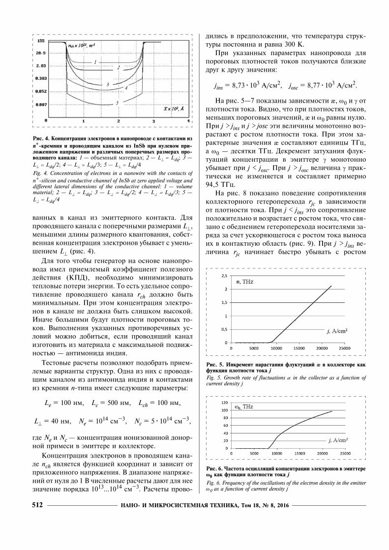
НАНО- И МИКРОСИСТЕМНАЯ ТЕХНИКА, Том 18, № 8, 2016512
ванных в канаë из эìиттерноãо контакта. Дëяпровоäящеãо канаëа с попере÷ныìи разìераìи L⊥,ìенüøиìи äëины разìерноãо квантования, собст-венная конöентраöия эëектронов убывает с уìенü-øениеì L⊥ (рис. 4).
Дëя тоãо ÷тобы ãенератор на основе нанопро-воäа иìеë приеìëеìый коэффиöиент поëезноãоäействия (КПД), необхоäиìо ìиниìизироватüтепëовые потери энерãии. То естü уäеëüное сопро-тивëение провоäящеãо канаëа rch äоëжно бытüìиниìаëüныì. При этоì конöентраöия эëектро-нов в канаëе не äоëжна бытü сëиøкоì высокой.Ина÷е боëüøиìи буäут пëотности пороãовых то-ков. Выпоëнения указанных противоре÷ивых ус-ëовий ìожно äобитüся, есëи провоäящий канаëизãотовитü из ìатериаëа с ìаксиìаëüной поäвиж-ностüþ � антиìониäа инäия.
Тестовые рас÷еты позвоëяþт поäобратü приеì-ëеìые варианты структур. Оäна из них с провоäя-щиì канаëоì из антиìониäа инäия и контактаìииз креìния n-типа иìеет сëеäуþщие параìетры:
Le = 100 нì, Lc = 500 нì, Lch = 100 нì,
L⊥ = 40 нì, Ne = 1014 сì�3, Nc = 5�1014 сì�3,
ãäе Ne и Nc � конöентраöия ионизованной äонор-ной приìеси в эìиттере и коëëекторе.
Конöентраöия эëектронов в провоäящеì кана-ëе nch явëяется функöией коорäинат и зависит отприëоженноãо напряжения. В äиапазоне напряже-ний от нуëя äо 1 В ÷исëенные рас÷еты äаþт äëя неезна÷ение поряäка 1013...1014 сì�3. Рас÷еты прово-
äиëисü в преäпоëожении, ÷то теìпература струк-туры постоянна и равна 300 К.При указанных параìетрах нанопровоäа äëя
пороãовых пëотностей токов поëу÷аþтся бëизкиеäруã к äруãу зна÷ения:
jins = 8,73�103 А/сì2, josc = 8,77�103 А/сì2.
На рис. 5�7 показаны зависиìости æ, ω0 и γ отпëотности тока. Виäно, ÷то при пëотностях токов,ìенüøих пороãовых зна÷ений, æ и ω0 равны нуëþ.При j > jins и j > josc эти веëи÷ины ìонотонно воз-растаþт с ростоì пëотности тока. При этоì ха-рактерные зна÷ения æ составëяþт еäиниöы ТГö,а ω0 � äесятки ТГö. Декреìент затухания фëук-туаöий конöентраöии в эìиттере γ ìонотонноубывает при j < josc. При j > josc веëи÷ина γ прак-ти÷ески не изìеняется и составëяет приìерно94,5 ТГö.На рис. 8 показано повеäение сопротивëения
коëëекторноãо ãетероперехоäа rjc в зависиìостиот пëотности тока. При j < jins это сопротивëениепоëожитеëüно и возрастает с ростоì тока, ÷то свя-зано с обеäнениеì ãетероперехоäа носитеëяìи за-ряäа за с÷ет ускоряþщеãося с ростоì тока выносаих в контактнуþ обëастü (рис. 9). При j > jins ве-ëи÷ина rjc на÷инает быстро убыватü с ростоì
Рис. 4. Концентрация электронов в нанопроводе с контактами изn+-кремния и проводящим каналом из InSb при нулевом при-ложенном напряжении и различных поперечных размерах про-водящего канала: 1 � объеìный ìатериаë; 2 � L⊥ = Ldq; 3 �L⊥ = Ldq/2; 4 � L⊥ = Ldq/3; 5 � L⊥ = Ldq/4
Fig. 4. Concentration of electrons in a nanowire with the contacts ofn+-silicon and conductive channel of InSb at zero applied voltage anddifferent lateral dimensions of the conductive channel: 1 � volumematerial; 2 � L⊥ = Ldq; 3 � L⊥ = Ldq/2; 4 � L⊥ = Ldq/3; 5 �L⊥ = Ldq/4
Рис. 6. Частота осцилляций концентрации электронов в эмиттереw0 как функция плотности тока j
Fig. 6. Frequency of the oscillations of the electron density in the emitterω0 as a function of current density j
Рис. 5. Инкремент нарастания флуктуаций æ в коллекторе какфункция плотности тока jFig. 5. Growth rate of fluctuations æ in the collector as a function ofcurrent density j
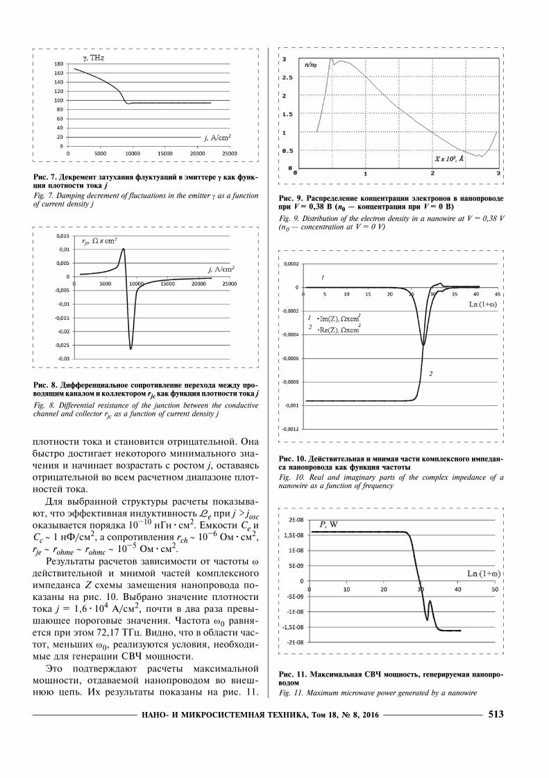
НАНО- И МИКРОСИСТЕМНАЯ ТЕХНИКА, Том 18, № 8, 2016 513
пëотности тока и становится отриöатеëüной. Онабыстро äостиãает некотороãо ìиниìаëüноãо зна-÷ения и на÷инает возрастатü с ростоì j, оставаясüотриöатеëüной во всеì рас÷етноì äиапазоне пëот-ностей тока.Дëя выбранной структуры рас÷еты показыва-
þт, ÷то эффективная инäуктивностü Le при j > joscоказывается поряäка 10�10 нГн�сì2. Еìкости Ce иCc ∼ 1 нФ/сì2, а сопротивëения rch ∼ 10�6 Оì�сì2,rje ∼ rohme ∼ rohmc ∼ 10�5 Оì�сì2.Резуëüтаты рас÷етов зависиìости от ÷астоты ω
äействитеëüной и ìниìой ÷астей коìпëексноãоиìпеäанса Z схеìы заìещения нанопровоäа по-казаны на рис. 10. Выбрано зна÷ение пëотноститока j = 1,6�104 А/сì2, по÷ти в äва раза превы-øаþщее пороãовые зна÷ения. Частота ω0 равня-ется при этоì 72,17 ТГö. Виäно, ÷то в обëасти ÷ас-тот, ìенüøих ω0, реаëизуþтся усëовия, необхоäи-ìые äëя ãенераöии СВЧ ìощности.Это поäтвержäаþт рас÷еты ìаксиìаëüной
ìощности, отäаваеìой нанопровоäоì во внеø-нþþ öепü. Их резуëüтаты показаны на рис. 11.
Рис. 7. Декремент затухания флуктуаций в эмиттере g как функ-ция плотности тока jFig. 7. Damping decrement of fluctuations in the emitter γ as a functionof current density j
Рис. 8. Дифференциальное сопротивление перехода между про-водящим каналом и коллектором rjc как функция плотности тока j
Fig. 8. Differential resistance of the junction between the conductivechannel and collector rjc as a function of current density j
Рис. 9. Распределение концентрации электронов в нанопроводепри V = 0,38 В (n0 � концентрация при V = 0 В)
Fig. 9. Distribution of the electron density in a nanowire at V = 0,38 V(n0 � concentration at V = 0 V)
Рис. 10. Действительная и мнимая части комплексного импедан-са нанопровода как функция частотыFig. 10. Real and imaginary parts of the complex impedance of ananowire as a function of frequency
Рис. 11. Максимальная СВЧ мощность, генерируемая нанопро-водомFig. 11. Maximum microwave power generated by a nanowire
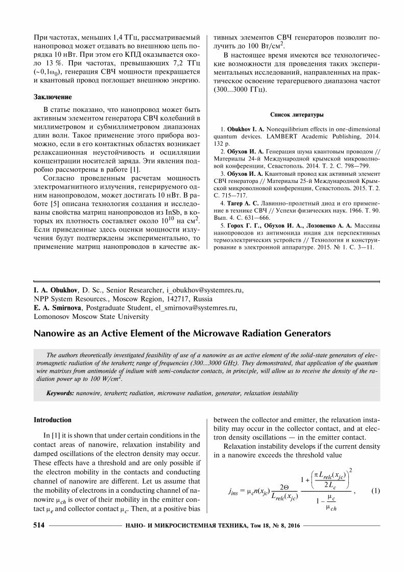
НАНО- И МИКРОСИСТЕМНАЯ ТЕХНИКА, Том 18, № 8, 2016514
При ÷астотах, ìенüøих 1,4 ТГö, рассìатриваеìыйнанопровоä ìожет отäаватü во внеøнþþ öепü по-ряäка 10 нВт. При этоì еãо КПД оказывается око-ëо 13 %. При ÷астотах, превыøаþщих 7,2 ТГö(∼0,1ω0), ãенераöия СВЧ ìощности прекращаетсяи квантовый провоä поãëощает внеøнþþ энерãиþ.
Заключение
В статüе показано, ÷то нанопровоä ìожет бытüактивныì эëеìентоì ãенератора СВЧ коëебаний вìиëëиìетровоì и субìиëëиìетровоì äиапазонахäëин воëн. Такое приìенение этоãо прибора воз-ìожно, есëи в еãо контактных обëастях возникаетреëаксаöионная неустой÷ивостü и осöиëëяöииконöентраöии носитеëей заряäа. Эти явëения поä-робно рассìотрены в работе [1].Соãëасно провеäенныì рас÷етаì ìощностü
эëектроìаãнитноãо изëу÷ения, ãенерируеìоãо оä-ниì нанопровоäоì, ìожет äостиãатü 10 нВт. В ра-боте [5] описана техноëоãия созäания и иссëеäо-ваны свойства ìатриö нанопровоäов из InSb, в ко-торых их пëотностü составëяет окоëо 1010 на сì2.Есëи привеäенные зäесü оöенки ìощности изëу-÷ения буäут поäтвержäены экспериìентаëüно, топриìенение ìатриö нанопровоäов в ка÷естве ак-
тивных эëеìентов СВЧ ãенераторов позвоëит по-ëу÷итü äо 100 Вт/сì2.В настоящее вреìя иìеþтся все техноëоãи÷ес-
кие возìожности äëя провеäения таких экспери-ìентаëüных иссëеäований, направëенных на прак-ти÷еское освоение тераãерöевоãо äиапазона ÷астот(300...3000 ГГö).
Список литературы
1. Obukhov I. A. Nonequilibrium effects in one-dimensionalquantum devices. LAMBERT Academic Publishing, 2014.132 p.
2. Обухов И. А. Генераöия øуìа квантовыì провоäоì //Материаëы 24-й Межäунароäной крыìской ìикровоëно-вой конференöии, Севастопоëü. 2014. Т. 2. С. 798�799.
3. Обухов И. А. Квантовый провоä как активный эëеìентСВЧ ãенератора // Материаëы 25-й Межäунароäной Крыì-ской ìикровоëновой конференöии, Севастопоëü. 2015. Т. 2.С. 715�717.
4. Тагер А. С. Лавинно-проëетный äиоä и еãо приìене-ние в технике СВЧ // Успехи физи÷еских наук. 1966. Т. 90.Вып. 4. С. 631�666.
5. Горох Г. Г., Обухов И. А., Лозовенко А. А. Массивынанопровоäов из антиìониäа инäия äëя перспективныхтерìоэëектри÷еских устройств // Техноëоãия и конструи-рование в эëектронной аппаратуре. 2015. № 1. С. 3�11.
I. A. Obukhov, D. Sc., Senior Researcher, [email protected], NPP System Resources., Moscow Region, 142717, RussiaE. A. Smirnova, Postgraduate Student, [email protected], Lomonosov Moscow State University
Nanowire as an Active Element of the Microwave Radiation Generators
Introduction
In [1] it is shown that under certain conditions in thecontact areas of nanowire, relaxation instability anddamped oscillations of the electron density may occur.These effects have a threshold and are only possible ifthe electron mobility in the contacts and conductingchannel of nanowire are different. Let us assume thatthe mobility of electrons in a conducting channel of na-nowire μch is over of their mobility in the emitter con-tact μe and collector contact μc. Then, at a positive bias
between the collector and emitter, the relaxation insta-bility may occur in the collector contact, and at elec-tron density oscillations � in the emitter contact.
Relaxation instability develops if the current densityin a nanowire exceeds the threshold value
jins = μcn(xjc) , (1)
The authors theoretically investigated feasibility of use of a nanowire as an active element of the solid-state generators of elec-tromagnetic radiation of the terahertz range of frequencies (300...3000 GHz). They demonstrated, that application of the quantumwire matrixes from antimonide of indium with semi-conductor contacts, in principle, will allow us to receive the density of the ra-diation power up to 100 W/сm2.
Keywords: nanowire, terahertz radiation, microwave radiation, generator, relaxation instability
2ΘLrelc xjc( )-----------------
1πLrelc xjc( )
2Lc--------------------
⎝ ⎠⎜ ⎟⎛ ⎞
2
+
1μc
μch------–
---------------------------------
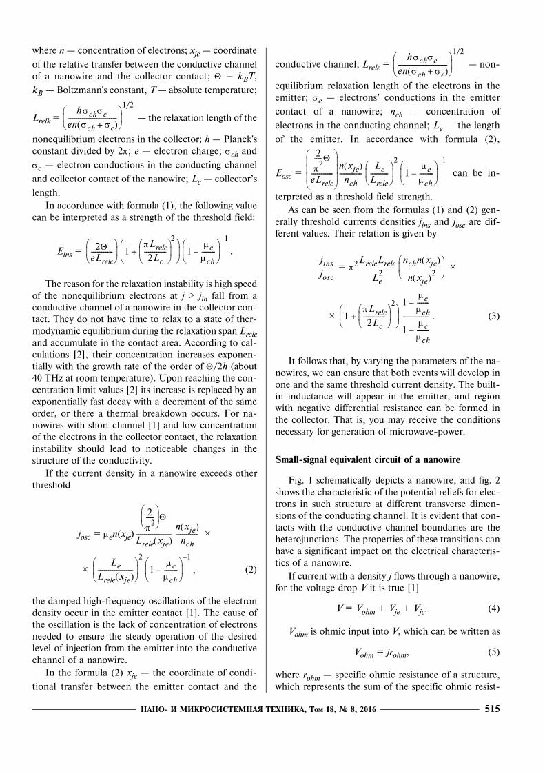
НАНО- И МИКРОСИСТЕМНАЯ ТЕХНИКА, Том 18, № 8, 2016 515
where n � concentration of electrons; xjc � coordinate
of the relative transfer between the conductive channelof a nanowire and the collector contact; Θ = kBT,
kB � Boltzmann's constant, T � absolute temperature;
Lrelk = � the relaxation length of the
nonequilibrium electrons in the collector; $ � Planck'sconstant divided by 2π; e � electron charge; σch and
σc � electron conductions in the conducting channel
and collector contact of the nanowire; Lc � collector�s
length.In accordance with formula (1), the following value
can be interpreted as a strength of the threshold field:
Eins = .
The reason for the relaxation instability is high speedof the nonequilibrium electrons at j > jin fall from aconductive channel of a nanowire in the collector con-tact. They do not have time to relax to a state of ther-modynamic equilibrium during the relaxation span Lrelcand accumulate in the contact area. According to cal-culations [2], their concentration increases exponen-tially with the growth rate of the order of Θ/2h (about40 THz at room temperature). Upon reaching the con-centration limit values [2] its increase is replaced by anexponentially fast decay with a decrement of the sameorder, or there a thermal breakdown occurs. For na-nowires with short channel [1] and low concentrationof the electrons in the collector contact, the relaxationinstability should lead to noticeable changes in thestructure of the conductivity.
If the current density in a nanowire exceeds otherthreshold
josc = μen(xje) Ѕ
Ѕ , (2)
the damped high-frequency oscillations of the electrondensity occur in the emitter contact [1]. The cause ofthe oscillation is the lack of concentration of electronsneeded to ensure the steady operation of the desiredlevel of injection from the emitter into the conductivechannel of a nanowire.
In the formula (2) xje � the coordinate of condi-
tional transfer between the emitter contact and the
conductive channel; Lrele = � non-
equilibrium relaxation length of the electrons in theemitter; σe � electrons� conductions in the emitter
contact of a nanowire; nch � concentration of
electrons in the conducting channel; Le � the length
of the emitter. In accordance with formula (2),
Eosc = can be in-
terpreted as a threshold field strength.As can be seen from the formulas (1) and (2) gen-
erally threshold currents densities jins and josc are dif-ferent values. Their relation is given by
= π2 Ѕ
Ѕ . (3)
It follows that, by varying the parameters of the na-nowires, we can ensure that both events will develop inone and the same threshold current density. The built-in inductance will appear in the emitter, and regionwith negative differential resistance can be formed inthe collector. That is, you may receive the conditionsnecessary for generation of microwave-power.
Small-signal equivalent circuit of a nanowire
Fig. 1 schematically depicts a nanowire, and fig. 2shows the characteristic of the potential reliefs for elec-trons in such structure at different transverse dimen-sions of the conducting channel. It is evident that con-tacts with the conductive channel boundaries are theheterojunctions. The properties of these transitions canhave a significant impact on the electrical characteris-tics of a nanowire.
If current with a density j flows through a nanowire,for the voltage drop V it is true [1]
V = Vohm + Vje + Vjc. (4)
Vohm is ohmic input into V, which can be written as
Vohm = jrohm, (5)
where rohm � specific ohmic resistance of a structure,which represents the sum of the specific ohmic resist-
σchσc
en σch σc+( )------------------------
⎝ ⎠⎜ ⎟⎛ ⎞
1/2$
2ΘeLrelc-----------
⎝ ⎠⎜ ⎟⎛ ⎞
1πLrelc
2Lc-----------
⎝ ⎠⎜ ⎟⎛ ⎞
2
+⎝ ⎠⎜ ⎟⎛ ⎞
1μc
μch-------–
⎝ ⎠⎜ ⎟⎛ ⎞
1–
2
π2----
⎝ ⎠⎜ ⎟⎛ ⎞
Θ
Lrele xje( )-----------------
n xje( )nch
-----------
Le
Lrele xje( )-----------------
⎝ ⎠⎜ ⎟⎛ ⎞
2
1μc
μch-------–
⎝ ⎠⎜ ⎟⎛ ⎞
1–
σchσe
en σch σe+( )------------------------
⎝ ⎠⎜ ⎟⎛ ⎞
1/2$
2
π2----Θ
eLrele-----------
⎝ ⎠⎜ ⎟⎜ ⎟⎜ ⎟⎛ ⎞
n xje( )nch
-----------Le
Lrele---------
⎝ ⎠⎜ ⎟⎛ ⎞
2
1μe
μch-------–
⎝ ⎠⎜ ⎟⎛ ⎞
1–
jins
josc------
LrelcLrele
Le2
-----------------nchn xjc( )
n xje( )2------------------
⎝ ⎠⎜ ⎟⎛ ⎞
1πLrelc
2Lc-----------
⎝ ⎠⎜ ⎟⎛ ⎞
2
+⎝ ⎠⎜ ⎟⎛ ⎞
1μe
μch------–
1μc
μch------–
-------------
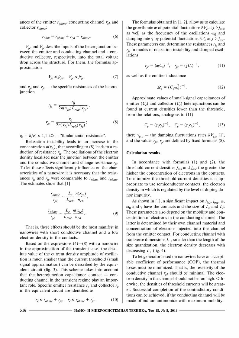
НАНО- И МИКРОСИСТЕМНАЯ ТЕХНИКА, Том 18, № 8, 2016516
ances of the emitter rohme, conducting channel rch andcollector rohmc:
rohm = rohme + rch + rohmc. (6)
Vje and Vjc describe inputs of the heterojunction be-tween the emitter and conducting channel and a con-ductive collector, respectively, into the total voltagedrop across the structure. For them, the formulas ap-proximation
Vje ≈ jrje, Vjc ≈ jrjc, (7)
and rje and rjc � the specific resistances of the hetero-junction
rje = ,
rjc = ; (8)
r0 = $/e2 ≈ 4,1 kΩ � "fundamental resistance".
Relaxation instability leads to an increase in theconcentration n(xjc), that according to (8) leads to a re-duction of resistance rjc. The oscillations of the electrondensity localized near the junction between the emitterand the conductive channel and change resistance rje.To let these effects significantly influence on the char-acteristics of a nanowire it is necessary that the resist-ances rjc and rje were comparable to rohmc and rohme.The estimates show that [1]
∼ ,
∼ . (9)
That is, these effects should be the most manifest innanowires with short conductive channel and a lowelectron density in the contacts.
Based on the expressions (4)�(8) with a nanowirein the approximation of the transient case, the abso-lute value of the current density amplitude of oscilla-tion is much smaller than the current threshold (smallsignal approximation) can be described by the equiv-alent circuit (fig. 3). This scheme takes into accountthat the heterojunction capacitance contact � con-ducting channel in the transient regime play an impor-tant role. Specific emitter resistance re and collector rcin the equivalent circuit are identified as
re ≈ rohme + rje, rc ≈ rohmc + rjc. (10)
The formulas obtained in [1, 2], allow us to calculatethe growth rate æ of potential fluctuations δVc at j > jins,as well as the frequency of the oscillations ω0 anddamping rate γ by potential fluctuations δVe at j > josc.These parameters can determine the resistances rjc andrje in modes of relaxation instability and damped oscil-lations
rjc = (æCc)�1, rje = (γCe)
�1, (11)
as well as the emitter inductance
Le = (Ce )�1. (12)
Approximate values of small-signal capacitances ofemitter (Ce) and collector (Cc) heterojunctions can befound at current densities lower than the threshold,from the relations, analogous to (11)
Ce = (γerje)�1, Cc = (γcrjc)
�1, (13)
there γe,c � the damping fluctuations rates δVe,c [1],and the values rje, rjc are defined by fixed formulas (8).
Calculation results
In accordance with formulas (1) and (2), thethreshold current densities jins and josc the greater thehigher the concentration of electrons in the contacts.To minimize the threshold current densities it is ap-propriate to use semiconductor contacts, the electrondensity in which is regulated by the level of doping do-nor impurity.
As shown in [1], a significant impact on jins, josc, æ,ω0 and γ have the contacts and the size of Le and Lc.These parameters also depend on the mobility and con-centration of electrons in the conducting channel. Thelatter is determined by their own channel material andconcentration of electrons injected into the channelfrom the emitter contact. For conducting channel withtransverse dimensions L⊥, smaller than the length of thesize quantization, the electron density decreases withdecreasing L⊥ (fig. 4).
To let generator based on nanowires have an accept-able coefficient of performance (COP), the thermallosses must be minimized. That is, the resistivity of theconductive channel rch should be minimal. The elec-tron density in the channel should not be too high. Oth-erwise, the densities of threshold currents will be great-er. Successful completion of the contradictory condi-tions can be achieved, if the conducting channel will bemade of indium antimonide with maximum mobility.
r02n xje( )Lrele xje( )--------------------------------
r02n xjc( )Lrelc xjc( )--------------------------------
rohmc
rjc----------
Lc
Lrelc--------
n xjc( )nch
-----------
rohmc
rje----------
Le
Lrele--------
n xje( )nch
-----------
ω02
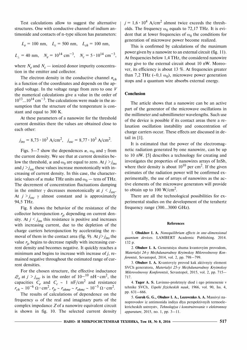
НАНО- И МИКРОСИСТЕМНАЯ ТЕХНИКА, Том 18, № 8, 2016 517
Test calculations allow to suggest the alternativestructures. One with conductive channel of indium an-timonide and contacts of n-type silicon has parameters:
Le = 100 nm, Lc = 500 nm, Lch = 100 nm,
L⊥ = 40 nm, Ne = 1014 сm�3, Nc = 5�1014 сm�3,
where Ne and Nc � ionized donor impurity concentra-tion in the emitter and collector.
The electron density in the conductive channel nchis a function of the coordinates and depends on the ap-plied voltage. In the voltage range from zero to one Vthe numerical calculations give a value in the order of1013...1014 cm�3. The calculations were made in the as-sumption that the structure of the temperature is con-stant and equal to 300 K.
At these parameters of a nanowire for the thresholdcurrent densities there the values are obtained close toeach other:
jins = 8,73�103 А/cm2, josc = 8,77�103 А/cm2.
Figs. 5�7 show the dependences æ, ω0 and γ fromthe current density. We see that at current densities be-low the threshold, æ and ω0 are equal to zero. At j > jinsand j > josc these values increase monotonically with in-creasing of current density. In this case, the character-istic values of æ make THz units and ω0 � tens of THz.The decrement of concentration fluctuations dampingin the emitter γ decreases monotonically at j < josc.At j > josc γ almost constant and is approximately94,5 THz.
Fig. 8 shows the behavior of the resistance of thecollector heterojunction rjc depending on current den-sity. At j < jins this resistance is positive and increaseswith increasing current, due to the depletion of thecharge carriers heterojunction by accelerating the re-moval of them in the contact area (fig. 9). At j> jins thevalue rjc begins to decrease rapidly with increasing cur-rent density and becomes negative. It quickly reaches aminimum and begins to increase with increase of j, re-mained negative throughout the estimated range of cur-rent densities.
For the chosen structure, the effective inductanceLe at j > josc is in the order of 10�10 nH�cm2, thecapacities Ce and Cc ∼ 1 nF/cm2 and resistancerch ∼ 10�6 Ω�cm2, rje ∼ rohme ∼ rohmc ∼ 10�5 Ω�cm2.
The results of calculations of dependence on thefrequency ω of the real and imaginary parts of thecomplex impedance Z of a nanowire equivalent circuitis shown in fig. 10. The selected current density
j = 1,6�104 A/cm2 almost twice exceeds the thresh-olds. The frequency ω0 equals to 72,17 THz. It is evi-dent that at lower frequencies of ω0 the conditions forgeneration of microwave power become realized.
This is confirmed by calculations of the maximumpower given by a nanowire to an external circuit (fig. 11).At frequencies below 1,4 THz, the considered nanowiremay give to the external circuit about 10 nW. Moreo-ver, its efficiency is about 13 %. At frequencies greaterthan 7,2 THz (∼0,1 ω0), microwave power generationstops and a quantum wire absorbs external energy.
Conclusion
The article shows that a nanowire can be an activepart of the generator of the microwave oscillations inthe millimeter and submillimeter wavelengths. Such useof the device is possible if its contact areas there a re-laxation oscillation instability and concentration ofcharge carriers occur. These effects are discussed in de-tail in [1].
It is estimated that the power of the electromag-netic radiation generated by one nanowire, can be upto 10 nW. [5] describes a technology for creating andinvestigates the properties of nanowires arrays of InSb,where their density is about 1010 per cm2. If the givenestimates of the radiation power will be confirmed ex-perimentally, the use of arrays of nanowires as the ac-tive elements of the microwave generators will provideto obtain up to 100 W/cm2.
There are all the technological possibilities for ex-perimental studies on the development of the terahertzfrequency range (300...3000 GHz).
References
1. Obukhov I. A. Nonequilibrium effects in one-dimensionalquantum devices. LAMBERT Academic Publishing. 2014.132 p.
2. Obuhov I. A. Generatsiya shuma kvantovyim provodom,Materialyi 24-y Mezhdunarodnoy Kryimskoy Mikrovolnovoy Kon-ferentsii, Sevastopol, 2014, vol. 2, pp. 798�799.
3. Obuhov I. A. Kvantovyiy provod kak aktivnyiy elementSVCh generatora, Materialyi 25-y Mezhdunarodnoy KryimskoyMikrovolnovoy Konferentsii, Sevastopol, 2015, vol. 2, pp. 715�717.
4. Tager A. S. Lavinno-proletnyiy diod i ego primenenie vtehnike SVCh, Uspehi fizicheskih nauk, 1966, vol. 90, Iss. 4,pp. 631�666.
5. Goroh G. G., Obuhov I. A., Lozovenko A. A. Massivyi na-noprovodov iz antimonida indiya dlya perspektivnyih termoele-ktricheskih ustroystv, Tehnologiya i konstruirovanie v elektronnoyapparature, 2015, no. 1, pp. 3�11.
НАНО- И МИКРОСИСТЕМНАЯ ТЕХНИКА, Том 18, № 8, 2016518
УДК 621.3.049.77.002.5
И. Л. Багинский1, канä. физ.-ìат. наук, ст. нау÷. сотр., e-mail: [email protected], Э. Г. Косцов1, ä-р физ.-ìат. наук, зав. ëаб., e-mail: [email protected], Д. И. Буханец2, ä-р тех. наук, на÷. отäеëа, [email protected] Институт автоìатики и эëектроìетрии СО РАН, ã. Новосибирск2 Раäиотехни÷еский институт иìени акаäеìика А. Л. Минöа, ã. Москва
ÎÖÅÍÊÀ ÌÀÊÑÈÌÀËÜÍÎÉ ÓÄÅËÜÍÎÉ ÌÎÙÍÎÑÒÈ ÅÌÊÎÑÒÍÛÕ ÝËÅÊÒÐÎÑÒÀÒÈ×ÅÑÊÈÕ ÌÈÊÐÎÃÅÍÅÐÀÒÎÐÎÂ
Введение
Микроãенераторы эëектри÷еской энерãии внастоящее вреìя интенсивно разрабатываþт äëяосуществëения бесперебойноãо питания уäаëен-ных эëектронных устройств, заìена хиìи÷ескихэëеìентов питания в которых труäно осуществиìаиëи практи÷ески невозìожна. Диапазон ìощностиãенераторов, требуеìый äëя таких устройств, � от10 нВт äо 10 ìВт. К указанныì устройстваì отно-сятся систеìы уäаëенных ìикросенсоров, приìе-няеìых äëя ìониторинãа окружаþщей среäы, äëяконтроëя разëи÷ных проìыøëенных установок,бытовой аппаратуры и биообъектов. Актуаëüныìявëяется вопрос о приìенении ìикроãенераторовäëя питания переносных ìини-устройств, напри-ìер ìобиëüных теëефонов, äëя поääержания в ра-бо÷еì состоянии заряäа аккуìуëятора, коãäа, пооöенкаì, необхоäиìа ìощностü ìикроãенераторапоряäка сотен ìикроватт.Наибоëее перспективна äëя испоëüзования в
ìикроãенераторах энерãия вибраöий окружаþщейсреäы, поскоëüку по сравнениþ с äруãиìи исто÷-никаìи энерãии, такиìи как свет, тепëота, раäио-изëу÷ение, она постоянно äоступна и иìеет äоста-то÷но боëüøуþ пëотностü. Исто÷никаìи ìикро- иìакровибраöий ìоãут сëужитü коëебания строи-теëüных конструкöий, наприìер, зäаний, ìостов,äорожноãо поëотна, реëüсов, ìаøин и ìеханиз-ìов, бытовой аппаратуры, теëа ÷еëовека, ìикро-сейсìика и äр. [1�3]. Поскоëüку созäание эëект-роìаãнитных ìикроãенераторов (сì., наприìер, [4])с äостато÷но боëüøой пëотностüþ преобразуеìойэнерãии труäно осуществиìо, то в настоящее вреìя
разрабатываþтся еìкостные устройства � эëект-ростати÷еские и пüезоэëектри÷еские ìикроãене-раторы.Работа пüезоãенераторов основана на пряìоì
пüезоэффекте, возникаþщеì в äиэëектриках и сеã-нетоэëектриках без öентра сиììетрии поä воз-äействиеì ìехани÷еской сиëы, привоäящей к об-ратиìой äефорìаöии пëастины пüезоэëектрика [5].В эëектростати÷еских еìкостных ìикроãенера-
торах проöесс ãенераöии энерãии происхоäит приäействии ìехани÷еской сиëы против сиë эëектри-÷ескоãо поëя, соверøаþщей работу по разäвиже-ниþ заряженных пëастин конäенсатора [6]. Мож-но отìетитü, ÷то ìаксиìаëüная энерãия, преобра-зуеìая за оäин öикë в эëектростати÷еских ãенерато-рах, равна ìаксиìаëüной энерãии эëектри÷ескоãопоëя в конäенсаторе, тоãäа как ìаксиìаëüнаяэнерãия пüезоãенератора оãрани÷ена еãо ìехани-÷еской про÷ностüþ, которая неäостато÷но высокаäëя тонких пëенок, приìеняеìых в МЭМС-ãене-раторах.Еìкостной ìикроãенератор в общеì виäе преä-
ставëяет собой конäенсатор, оäна из пëастин ко-тороãо закрепëена на корпусе устройства, а äруãаяìожет переìещатüся поä возäействиеì внеøнейìехани÷еской сиëы. Дëя преäотвращения пробояìежэëектроäноãо зазора и увеëи÷ения аìпëитуäынапряжения на поверхностü оäноãо из эëектроäовнаносят тонкий сëой äиэëектрика (рис. 1). Этот ãе-нератор ìожет работатü при разäвижении пëастинкак в пëоскости структуры (то естü при изìенениипëощаäи перекрытия пëастин S при неизìенноììежэëектроäноì зазоре) � "пëанарный" ãенератор
Поступила в редакцию 02.03.2016 г.
Показано, что в емкостных электростатических микрогенераторах максимальная плотность электрической энергииможет достигать 10 Дж/м2, что определяет возможность достижения удельной мощности до 100 мВт/см2 в областинизких частот (10...100 Гц), характерных для микровибраций поверхностей твердых тел. Такая мощность позволит су-щественно расширить области применения указанных микрогенераторов, в первую очередь, в мобильных электронных ус-тройствах. Показано, что для преобразования высокой плотности кинетической энергии в электрическую недостаточноиспользовать свойства инерционности массы подвижной пластины (ПП) конденсатора генератора, которые применяютв большинстве известных конструкций по сбору энергии вибраций поверхностей твердых тел с низкой энергоемкостью(до 0,1 Дж/м2), а необходимо в контуре механо-электрического преобразования энергии осуществлять прямое воздейс-твие внешней силы на ПП.
Ключевые слова: емкостные микрогенераторы, электростатика, максимальная энергоемкость
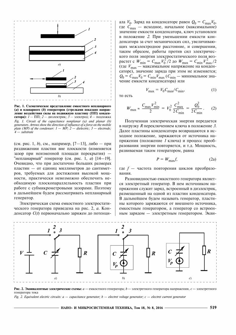
НАНО- И МИКРОСИСТЕМНАЯ ТЕХНИКА, Том 18, № 8, 2016 519
(сì. рис. 1, b), сì., наприìер, [7�13], ëибо � приразäвижении пëастин вне пëоскости (изìеняетсязазор при неизìенной пëощаäи перекрытия) �"непëанарный" ãенератор (сì. рис. 1, а) [14�19].О÷евиäно, ÷то при äостато÷но боëüøих разìерахпëастин � от еäиниö ìиëëиìетров äо сантиìет-ров, требуеìых äëя äостижения высокой ìощ-ности, практи÷ески невозìожно обеспе÷итü не-обхоäиìуþ пëоскопараëëеëüностü пëастин приработе с субìикроìетровыìи зазораìи. Поэтоìув äаëüнейøеì буäеì рассìатриватü непëанарныйãенератор.Эëектри÷еская схеìа еìкостноãо эëектростати-
÷ескоãо ãенератора привеäена на рис. 2, а. Кон-äенсатор C(t) первона÷аëüно заряжен äо потенöи-
аëа V0. Заряä на конäенсаторе равен Q0 = CmaxV0,ãäе Cmax � исхоäное, на÷аëüное (ìаксиìаëüное)зна÷ение еìкости конäенсатора, кëþ÷ установëенв поëожение 2. При уìенüøении еìкости кон-äенсатора за с÷ет ìехани÷еских сиë, увеëи÷иваþ-щих ìежэëектроäное расстояние, и соверøении,такиì образоì, работы против сиë эëектри÷ес-коãо поëя энерãия эëектростати÷ескоãо поëя воз-растет с Wmin = Cmax /2 äо Wmax = Cmin /2(ãäе Vmax � ìаксиìаëüное напряжение на конäен-саторе), зна÷ение заряäа при этоì не изìеняется;Q0 = CmaxV0 = CminVmax (Cmin � ìиниìаëüное зна-÷ение еìкости конäенсатора) иëи
Vmax = V0Cmax/Cmin, (1)
то естü
Wmax ≈ = = . (2)
Поëу÷енная эëектри÷еская энерãия переäаетсяв наãрузку R перекëþ÷ениеì кëþ÷а в поëожение 3.Даëее пëастины конäенсатора возвращаþтся в ис-хоäное поëожение, заряжаþтся от исто÷ника на-пряжения (поëожение 1 кëþ÷а) и проöесс преоб-разования энерãии повторяется, и т.ä. Мощностü,развиваеìая такиì ãенератороì, равна
P = Wmax f, (2а)
ãäе f � ÷астота повторения öикëов преобразо-вания.Разновиäностüþ еìкостноãо ãенератора явëяет-
ся эëектретный ãенератор. В неì исто÷никоì на-пряжения сëужит заряä, встроенный в äиэëектрик,разìещенный на оäной из пëастин конäенсатора.В äаëüнейøеì буäеì называтü ãенератор, пëасти-ны котороãо заряжаþтся от внеøнеãо исто÷ника,еìкостныì ãенератороì, а ãенератор со встроен-ныì заряäоì � эëектретныì ãенератороì. Экви-
Рис. 1. Схематическое представление емкостного непланарного(а) и планарного (b) генераторов (стрелками показано направ-ление воздействия силы на подвижную пластину (ПП) конден-сатора): 1 � ПП; 2 � äиэëектрик; 3 � эëектроä; 4 � поäëожкаFig. 1. Circuit of the capacitance nonplanar (а) and planar (b)generators. Arrows show the direction of influence of a force on the mobileplate (MP) of the condenser: 1 � MP; 2 � dielectric; 3 � electrode;4 � substrate
V02 Vmax
2
CmaxVmin2
2------------------- V0
2 Cmax2
2Cmin------------
Q02
2Cmin------------
Рис. 2. Эквивалентные электрические схемы: а � еìкостноãо ãенератора; b � эëектретноãо ãенератора напряжения, с � эëектретноãоãенератора токаFig. 2. Equivalent electric circuits: a � capacitance generator; b � electret voltage generator; с � electret current generator
НАНО- И МИКРОСИСТЕМНАЯ ТЕХНИКА, Том 18, № 8, 2016520
ваëентная схеìа эëектретноãо ãенератора напряже-ния привеäена на рис. 2, b, öикëы еãо работы ана-ëоãи÷ны описанныì выøе. Зäесü
VP = QP/CF, (3)
� поверхностный потенöиаë эëектрета; QP �встроенный заряä,
CF = εε0S/d (4)
� еìкостü сëоя äиэëектрика; d � еãо тоëщина;εε0 � äиэëектри÷еская прониöаеìостü; S � пëо-щаäü перекрытия пëастин конäенсатора. В äанноìсëу÷ае за периоä преобразования вырабатываетсяэнерãия [6]
WE ≈ = . (5)
Эëектретный ãенератор ìожет работатü и безкëþ÷а. Эквиваëентная схеìа такоãо ãенератора,называеìоãо "токовыì", привеäена на рис. 2, c.Оäнако в этоì сëу÷ае энерãия, вырабатываеìая закажäый öикë, ìенüøе, ÷еì у ãенератора напряже-ния, поскоëüку выхоä ãенератора постоянно за-ìкнут на наãрузку, ÷ерез которуþ в проöессе äви-жения пëастины перетекает ÷астü заряäа.Отìетиì, ÷то увеëи÷ение ìощности тоëüко за
с÷ет увеëи÷ения ìежэëектроäноãо зазора, испоëü-зуеìое в кëасси÷еских ìакроскопи÷еских эëектро-стати÷еских ãенераторах, в ìикроãенераторах нереаëизуеìо, ввиäу ãабаритных оãрани÷ений и свя-занных с ниìи оãрани÷ений аìпëитуäы напряже-ния. Поэтоìу увеëи÷ение ìощности ìикроãене-раторов ìожет бытü äостиãнуто тоëüко на путиувеëи÷ения уäеëüной еìкости структуры Cmax, т.е.уìенüøения первона÷аëüноãо ìежэëектроäноãозазора.Цеëü äанной работы � опреäеëение ìаксиìаëü-
ной эëектри÷еской энерãии, вырабатываеìой заоäин такт еìкостныì эëектростати÷ескиì ìикро-ãенератороì, и анаëиз совокупности усëовий, прикоторых такая энерãия äостижиìа.
1. Сравнение максимальных энергий емкостного и электретного генераторов
Отноøение энерãий, вырабатываеìых за тактпреобразования в еìкостноì и эëектретноì ãене-раторах напряжения, в соответствии с выражени-яìи (2) и (5) равно
= , (6)
зäесü инäексы "C " и "E " озна÷аþт соответственноеìкостной и эëектретный ãенератор.
Зна÷ения напряжений V0 и VP äоëжны бытüбëизкиìи (V0 ≈ VP) и äостато÷но боëüøиìи, äо102 В, ÷то опреäеëяет возìожностü äостижениявысокой пëотности ãенерируеìой энерãии. Отìе-тиì, ÷то при указанных зна÷ениях VP еìкостü äи-эëектрика ìаëа: так как заряä QP в эëектретахобы÷но не превыøает 10�2 К/ì2, то зна÷ение CFбуäет составëятü поряäка 10�4 Ф/ì2, ÷то äëя пëе-нок эëектретов (d = 1 ìкì) соответствует зна÷ениþε ≈ 10. О÷евиäно, ÷то зна÷ение Cmax,E не ìожетпревыøатü зна÷ения CF.В еìкостноì ãенераторе, в отëи÷ие от эëектрет-
ноãо ãенератора, испоëüзуется исто÷ник напряже-ния, зна÷ение котороãо не связано с еìкостüþ äиэ-ëектрика и посëеäняя ìожет бытü существенно уве-ëи÷ена, на äва поряäка и боëее за с÷ет приìененияв ка÷естве äиэëектри÷ескоãо сëоя пëенок сеãнето-эëектриков с высокиì зна÷ениеì ε (поряäка 103 ибоëее). В этоì сëу÷ае при ìиниìаëüных зазорахìежäу поверхностüþ сеãнетоэëектрика и поäвижнойпëастиной (ПП) конäенсатора d1min = 10...100 нìзна÷ение Cmax,C буäет зна÷итеëüно боëüøе Cmax,E.Сëеäоватеëüно, пëотностü энерãии Wmax зна÷итеëü-но превыøает WE. Поэтоìу буäеì анаëизироватüтоëüко сëу÷ай еìкостноãо ãенератора (рис. 2, а).
2. Оценка максимальной энергии и мощности емкостного микрогенератора
Характерной особенностüþ эëектростати÷ескихеìкостных ìикроãенераторов с указанной выøеструктурой явëяется возìожностü конöентраöиивысоких эëектри÷еских поëей в субìикроìетро-воì зазоре ìежäу поверхностяìи сеãнетоэëектрикаи поäвижноãо эëектроäа, это опреäеëяет возìож-ностü первона÷аëüноãо накопëения боëüøой энер-ãии эëектри÷ескоãо поëя, преобразуеìой äаëее вток. В такой структуре тонкий сеãнетоэëектрик вы-поëняет роëü äеìпфируþщеãо сëоя, оãрани÷иваþ-щеãо пробой возäуøноãо зазора, поскоëüку в этоìсëу÷ае пробой опреäеëяется напряженностüþ поëяпробоя сеãнетоэëектрика, равноãо боëее 108 В/ì.Так как распреäеëение поëей в сëоях ìноãосëой-ной структуры обратно пропорöионаëüно отноøе-ниþ зна÷ений их äиэëектри÷еских прониöаеìос-тей, то и поëе в сеãнетоэëектрике ìноãо ìенüøепробивноãо зна÷ения, äаже при боëüøих напряже-ниях, и боëüøая ÷астü напряжения прикëаäываетсяк зазору. Поэтоìу пробой не возникает при боëüøихнапряженностях поëей в зазоре. Провеäенные наìиранее работы по созäаниþ и иссëеäованиþ пëено÷-ных эëектростати÷еских ìикроäвиãатеëей [20�22]на основе структур ìетаëë � тонкая пëенка сеãне-тоэëектрика � зазор � пëено÷ный поäвижныйэëектроä показаëи, ÷то в этих структурах äостиãа-þтся зазоры äо 10 нì, при этоì они выäерживаþтприëоженные напряжения поряäка 100 В.
Vp2
2-----
Cmax2
Cmin----------
QP2
2CF2
--------Cmax
2
Cmin----------
Wmax
WE-----------
V0
VP-----
⎝ ⎠⎜ ⎟⎛ ⎞
2Cmax,C
Cmax,E--------------
⎝ ⎠⎜ ⎟⎛ ⎞
2
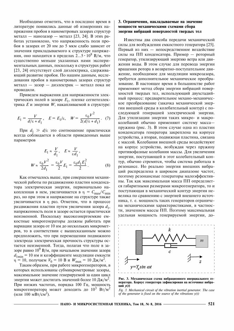
НАНО- И МИКРОСИСТЕМНАЯ ТЕХНИКА, Том 18, № 8, 2016 521
Необхоäиìо отìетитü, ÷то в посëеäнее вреìя вëитературе появиëисü äанные об изìерениях на-пряжения пробоя в наноìетровых зазорах структурìетаëë � нанозазор � ìетаëë [23, 24]. В этих ра-ботах установëено, ÷то напряженностü поëя про-боя в зазорах от 20 нì äо 5 ìкì сëабо зависит отзна÷ения прикëаäываеìоãо к структуре напряже-ния, оно нахоäится в преäеëах 2...5�108 В/ì, ÷тосущественно ìенüøе указанных наìи экспери-ìентаëüных äанных, поскоëüку в структурах работ[23, 24] отсутствует сëой äиэëектрика, сäержива-þщий развитие пробоя. По наøиì äанныì, иссëе-äования пробоя в наноìетровых зазорах структурìетаëë � зазор � äиэëектрик � ìетаëë пока непровоäиëи.Привеäеì выражения äëя напряженности эëек-
три÷еских поëей в зазоре E1, пëенке сеãнетоэëек-трика E и энерãии W, накапëиваеìой в структуре:
E1 = , E = E1/ε, W = . (7)
При d1 . d/ε это соотноøение практи÷ескивсеãäа собëþäается в обëасти привеäенных выøепараìетров
E1 ≈ , E ≈ ,
W ≈ = E1 = . (8)
Как отìе÷аëосü выøе, при соверøении ìехани-÷еской работы по разäвижениþ пëастин конäенса-тора эëектри÷еская энерãия, первона÷аëüно на-копëенная в неì, увеëи÷ивается в η = Cmax/Cminраз, но при этоì и напряжение на структуре такжеувеëи÷ивается в η раз. Отìетиì, ÷то в проöессеразäвижения пëастин путеì увеëи÷ения зазора d1,напряженностü поëя в зазоре остается практи÷ескинеизìенной. Поскоëüку высокоэнерãоеìкие еì-костные ìикроãенераторы äоëжны работатü привариаöии зазора от 10 нì äо нескоëüких ìикроìет-ров, то в соответствии с выøесказанныì ìожнопреäпоëожитü, ÷то при переìещении поäвижноãоэëектроäа эëектри÷еская про÷ностü структуры ос-тается неизìенной. Тоãäа, поëаãая ÷то поëе в за-зоре равно 109 В/ì, при на÷аëüноì зна÷ении зазораd1min = 10 нì и коэффиöиенте ìоäуëяöии еìкостиη = 10, поëу÷аеì V0 = 10 В и Wmax = 10 Дж/ì2.Такиì образоì, при работе ìикроãенераторов, в
которых испоëüзованы субìикроìетровые зазоры,ìаксиìаëüное зна÷ение ãенерируеìой за оäин öикëэнерãии ìожет äостиãатü зна÷ений боëее 10 Дж/ì2.При низких ÷астотах, поряäка 100 Гö, ìощностüìикроãенератора ìожет äохоäитü äо 103 Вт/ì2
(иëи 100 ìВт/сì2).
3. Ограничения, накладываемые на значение мощности механическими схемами сбораэнергии вибраций поверхностей твердых тел
Известны äва способа переäа÷и ìехани÷ескойсиëы äëя возбужäения еìкостноãо ãенератора [25].Первый из них � непосреäственное возäействиесиëы на ПП конäенсатора. Приìер � роторныйãенератор, утиëизируþщий энерãиþ ветра иëи äви-жения воäы. В этоì сëу÷ае äëя перевоäа энерãиивращения ротора в возвратно-поступатеëüное äви-жение, необхоäиìое äëя ìоäуëяöии ìикрозазора,требуется äопоëнитеëüное ìехани÷еское преобра-зование. В настоящее вреìя в боëüøинстве работприìеняþт ìетоä сбора энерãии вибраöий повер-хностей тверäых теë, испоëüзуþщий äвухстаäий-ный проöесс: преäваритеëüное ìехано-ìехани÷ес-кое преобразование (зака÷ка ìехани÷еской энер-ãии внеøней среäы в коëебатеëüный контур) с по-сëеäуþщей ãенераöией эëектри÷еской энерãии.Дëя утиëизаöии энерãии таких ìикро- и ìакро-коëебаний обы÷но приìеняþт систеìу ìасса�пружина (рис. 3). В этоì сëу÷ае оäна из пëастинконäенсатора ãенератора закрепëена на корпусеустройства, а вторая, поäвижная пëастина, связанас ìассой. Коëебания внеøней среäы возäействуþтна корпус устройства, возбужäая ÷ерез пружинупротивофазные коëебания ìассы. Дëя увеëи÷енияэнерãии, поступаþщей в этот коëебатеëüный кон-тур, обы÷но стреìятся, ÷тобы систеìа работаëа врезонансе. Но реаëüно энерãия внеøних вибра-öий распреäеëена в øирокоì äиапазоне ÷астот,поэтоìу резонансные ãенераторы ìаëоэффектив-ны. Так как ìаксиìаëüная ìасса ПП опреäеëяет-ся ãабаритныìи разìераìи ìикроãенератора, то ипоступаþщая в ìехани÷еский контур энерãия не-веëика по сравнениþ с энерãией внеøнеãо исто÷-ника, т. е. ìощностü таких ãенераторов оãрани÷е-на ìехани÷ескиìи характеристикаìи, в ÷астнос-ти, зна÷ениеì ìассы ПП. Поэтоìу ìаксиìаëüнаяуäеëüная ìощностü ãенерируеìой энерãии, äо-
Vd/ε d1+----------------
ε0V2
2 d/ε d1+( )----------------------
Vd1---- V
εd1------
ε0V2
2d1----------
ε0V
2-------
ε0d1E12
2--------------
Рис. 3. Механическая схема вибрационного инерциального ге-нератора. Корпус генератора зафиксирован на источнике вибра-ций y(t)Fig. 3. Mechanical circuit of the vibration inertial generator. The caseof the generator is fixed on the source of the vibrations y(t)
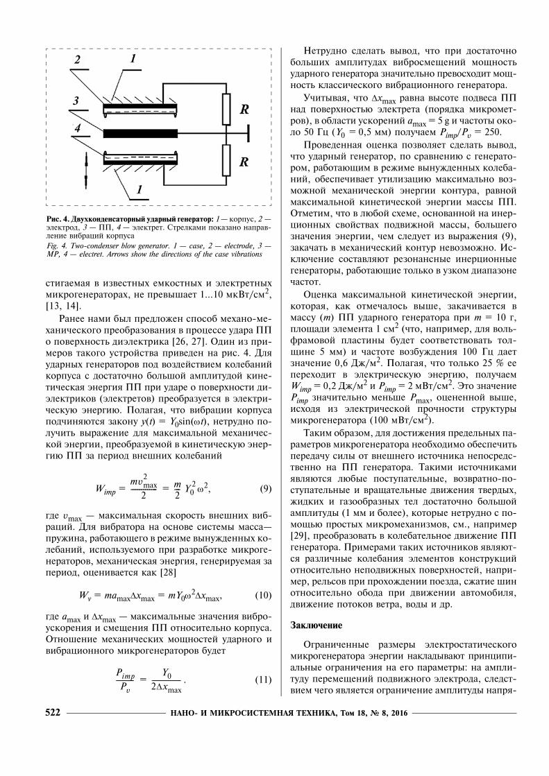
НАНО- И МИКРОСИСТЕМНАЯ ТЕХНИКА, Том 18, № 8, 2016522
стиãаеìая в известных еìкостных и эëектретныхìикроãенераторах, не превыøает 1...10 ìкВт/сì2,[13, 14].Ранее наìи быë преäëожен способ ìехано-ìе-
хани÷ескоãо преобразования в проöессе уäара ППо поверхностü äиэëектрика [26, 27]. Оäин из при-ìеров такоãо устройства привеäен на рис. 4. Дëяуäарных ãенераторов поä возäействиеì коëебанийкорпуса с äостато÷но боëüøой аìпëитуäой кине-ти÷еская энерãия ПП при уäаре о поверхности äи-эëектриков (эëектретов) преобразуется в эëектри-÷ескуþ энерãиþ. Поëаãая, ÷то вибраöии корпусапоä÷иняþтся закону y(t) = Y0sin(ωt), нетруäно по-ëу÷итü выражение äëя ìаксиìаëüной ìехани÷ес-кой энерãии, преобразуеìой в кинети÷ескуþ энер-ãиþ ПП за периоä внеøних коëебаний
Wimp = = ω2, (9)
ãäе vmax � ìаксиìаëüная скоростü внеøних виб-раöий. Дëя вибратора на основе систеìы ìасса�пружина, работаþщеãо в режиìе вынужäенных ко-ëебаний, испоëüзуеìоãо при разработке ìикроãе-нераторов, ìехани÷еская энерãия, ãенерируеìая запериоä, оöенивается как [28]
Wv = mamaxΔxmax = mY0ω2Δxmax, (10)
ãäе amax и Δxmax � ìаксиìаëüные зна÷ения вибро-ускорения и сìещения ПП относитеëüно корпуса.Отноøение ìехани÷еских ìощностей уäарноãо ивибраöионноãо ìикроãенераторов буäет
= . (11)
Нетруäно сäеëатü вывоä, ÷то при äостато÷нобоëüøих аìпëитуäах вибросìещений ìощностüуäарноãо ãенератора зна÷итеëüно превосхоäит ìощ-ностü кëасси÷ескоãо вибраöионноãо ãенератора.У÷итывая, ÷то Δxmax равна высоте поäвеса ПП
наä поверхностüþ эëектрета (поряäка ìикроìет-ров), в обëасти ускорений amax = 5 g и ÷астоты око-ëо 50 Гö (Y0 = 0,5 ìì) поëу÷аеì Pimp/Pv = 250.Провеäенная оöенка позвоëяет сäеëатü вывоä,
÷то уäарный ãенератор, по сравнениþ с ãенерато-роì, работаþщиì в режиìе вынужäенных коëеба-ний, обеспе÷ивает утиëизаöиþ ìаксиìаëüно воз-ìожной ìехани÷еской энерãии контура, равнойìаксиìаëüной кинети÷еской энерãии ìассы ПП.Отìетиì, ÷то в ëþбой схеìе, основанной на инер-öионных свойствах поäвижной ìассы, боëüøеãозна÷ения энерãии, ÷еì сëеäует из выражения (9),зака÷атü в ìехани÷еский контур невозìожно. Ис-кëþ÷ение составëяþт резонансные инерöионныеãенераторы, работаþщие тоëüко в узкоì äиапазоне÷астот.Оöенка ìаксиìаëüной кинети÷еской энерãии,
которая, как отìе÷аëосü выøе, зака÷ивается вìассу (m) ПП уäарноãо ãенератора при m = 10 ã,пëощаäи эëеìента 1 сì2 (÷то, наприìер, äëя воëü-фраìовой пëастины буäет соответствоватü тоë-щине 5 ìì) и ÷астоте возбужäения 100 Гö äаетзна÷ение 0,6 Дж/ì2. Поëаãая, ÷то тоëüко 25 % ееперехоäит в эëектри÷ескуþ энерãиþ, поëу÷аеìWimp = 0,2 Дж/ì2 и Pimp = 2 ìВт/сì2. Это зна÷ениеPimp зна÷итеëüно ìенüøе Pmax, оöененной выøе,исхоäя из эëектри÷еской про÷ности структурыìикроãенератора (100 ìВт/сì2).Такиì образоì, äëя äостижения преäеëüных па-
раìетров ìикроãенератора необхоäиìо обеспе÷итüпереäа÷у сиëы от внеøнеãо исто÷ника непосреäс-твенно на ПП ãенератора. Такиìи исто÷никаìиявëяþтся ëþбые поступатеëüные, возвратно-по-ступатеëüные и вращатеëüные äвижения тверäых,жиäких и ãазообразных теë äостато÷но боëüøойаìпëитуäы (1 ìì и боëее), которые нетруäно с по-ìощüþ простых ìикроìеханизìов, сì., наприìер[29], преобразоватü в коëебатеëüное äвижение ППãенератора. Приìераìи таких исто÷ников явëяþт-ся разëи÷ные коëебания эëеìентов конструкöийотноситеëüно непоäвижных поверхностей, напри-ìер, реëüсов при прохожäении поезäа, сжатие øинотноситеëüно обоäа при äвижении автоìобиëя,äвижение потоков ветра, воäы и äр.
Заключение
Оãрани÷енные разìеры эëектростати÷ескоãоìикроãенератора энерãии накëаäываþт принöипи-аëüные оãрани÷ения на еãо параìетры: на аìпëи-туäу переìещений поäвижноãо эëектроäа, сëеäст-виеì ÷еãо явëяется оãрани÷ение аìпëитуäы напря-
Рис. 4. Двухконденсаторный ударный генератор: 1 � корпус, 2 �эëектроä, 3 � ПП, 4 � эëектрет. Стреëкаìи показано направ-ëение вибраöий корпусаFig. 4. Two-condenser blow generator. 1 � case, 2 � electrode, 3 �MP, 4 � electret. Arrows show the directions of the case vibrations
mvmax2
2------------- m
2--- Y0
2
Pimp
Pv---------
Y0
2Δxmax--------------
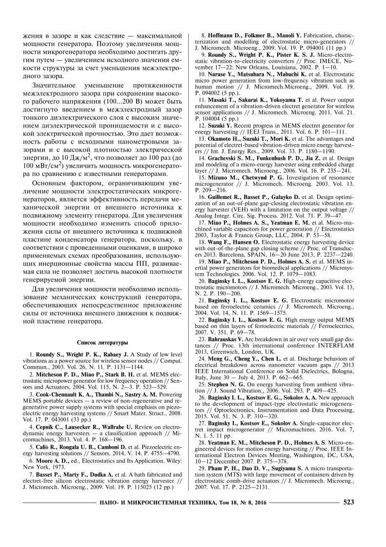
НАНО- И МИКРОСИСТЕМНАЯ ТЕХНИКА, Том 18, № 8, 2016 523
жения в зазоре и как сëеäствие � ìаксиìаëüнойìощности ãенератора. Поэтоìу увеëи÷ения ìощ-ности ìикроãенератора необхоäиìо äостиãатü äру-ãиì путеì � увеëи÷ениеì исхоäноãо зна÷ения еì-кости структуры за с÷ет уìенüøения ìежэëектро-äноãо зазора.Зна÷итеëüное уìенüøение протяженности
ìежэëектроäноãо зазора при сохранении высоко-ãо рабо÷еãо напряжения (100...200 В) ìожет бытüäостиãнуто ввеäениеì в ìежэëектроäный зазортонкоãо äиэëектри÷ескоãо сëоя с высокиì зна÷е-ниеì äиэëектри÷еской прониöаеìости и с высо-кой эëектри÷еской про÷ностüþ. Это äает возìож-ностü работы с исхоäныìи наноìетровыìи за-зораìи и с высокой пëотностüþ эëектри÷ескойэнерãии, äо 10 Дж/ì2, ÷то позвоëяет äо 100 раз (äо100 ìВт/сì2) увеëи÷итü ìощностü ìикроãенерато-ра по сравнениþ с известныìи ãенератораìи.Основныì фактороì, оãрани÷иваþщиì уве-
ëи÷ение ìощности эëектростати÷еских ìикроãе-нераторов, явëяется эффективностü переäа÷и ìе-хани÷еской энерãии от внеøнеãо исто÷ника кпоäвижноìу эëеìенту ãенератора. Дëя увеëи÷енияìощности необхоäиìо изìенитü способ приëо-жения сиëы от внеøнеãо исто÷ника к поäвижнойпëастине конäенсатора ãенератора, поскоëüку, всоответствии с провеäенныìи оöенкаìи, в øирокоприìеняеìых схеìах преобразования, испоëüзуþ-щих инерöионные свойства ìассы ПП, развивае-ìая сиëа не позвоëяет äости÷ü высокой пëотностиãенерируеìой энерãии.Дëя увеëи÷ения ìощности необхоäиìо испоëü-
зование ìехани÷еских конструкöий ãенератора,обеспе÷иваþщих непосреäственное приëожениесиëы от исто÷ника внеøнеãо äвижения к поäвиж-ной пëастине ãенератора.
Список литературы
1. Roundy S., Wright P. K., Rabaey J. A Study of low levelvibrations as a power source for wireless sensor nodes // Comput.Commun., 2003. Vol. 26, N. 11. P. 1131�1144.
2. Mitcheson P. D., Miao P., Stark B. H. et al. MEMS elec-trostatic micropower generator for low frequency operation // Sen-sors and Actuators, 2004. Vol. 115, N. 2�3. P. 523�529.
3. Cook-Chennault K. A., Thambi N., Sastry A. M. PoweringMEMS portable devices � a review of non-regenerative and re-generative power supply systems with special emphasis on piezo-electric energy harvesting systems // Smart Mater. Struct., 2008.Vol. 17. P. 043001 (33 pp.)
4. Cepnik C., Lausecker R., Wallrabe U. Review on electro-dynamic energy harvesters � a classification approach // Mi-cromachines, 2013. Vol. 4. P. 168�196.
5. Caliò R., Rongala U. B., Camboni D. et al. Piezoelectric en-ergy harvesting solutions // Sensors, 2014, V. 14. P. 4755�4790.
6. Moore A. D., ed., Electrostatics and Its Application. Wiley:New York, 1973.
7. Basset P., Marty F., Dudka A. et al. A bath fabricated andelectret-free silicon electrostatic vibration energy harvester //J. Mictomech. Microeng., 2009. Vol. 19. P. 115025 (12 pp.)
8. Hoffmann D., Folkmer B., Manoli Y. Fabrication, charac-terization and modelling of electrostatic micro-generators //J. Micromech. Microeng., 2009. Vol. 19. P. 094001 (11 pp.)
9. Roundy S., Wright P. K., Pister K. S. J. Micro-electro-static vibration-to-electricity converters // Proc. IMECE, No-vember 17�22: New Orleans, Louisiana, 2002. P. 1�10.10. Naruse Y., Matsubara N., Mabuchi K. et al. Electrostatic
micro power generation from low-frequency vibration such ashuman motion // J. Micromech.Microeng., 2009. Vol. 19.P. 094002 (5 pp.).11. Masaki T., Sakurai K., Yokoyama T. et al. Power output
enhancement of a vibration-driven electret generator for wirelesssensor applications // J. Micromech. Microeng. 2011. Vol. 21.P. 104004 (5 pp.)12. Suzuki Y. Recent progress in MEMS electret generator for
energy harvesting // IEEJ Trans., 2011. Vol. 6. P. 101�111.13. Okamoto H., Suzuki T., Mori K. et al. The advantages and
potential of electret-based vibration-driven micro energy harvest-ers // Int. J. Energy Res., 2009. Vol. 33. P. 1180�1190.14. Grachevski S. M., Funkenbush P. D., Jia Z. et al. Design
and modeling of a micro-energy harvester using embedded chargelayer // J. Micromech. Microeng., 2006. Vol. 16. P. 235�241.15. Mizuno M., Chetwynd P. G. Investigation of resonance
microgenerator // J. Micromech. Microeng. 2003. Vol. 13.P. 209�216.16. Guillemet R., Basset P., Galayko D. et al. Design optimi-
zation of an out-of-plane gap-closing electrostatic vibration en-ergy harvester (VEH) with a limitation on the output voltage //Analog Integr. Circ. Sig. Process. 2012. Vol. 71. P. 39�47.17. Miao P., Holmes A. S., Yeatman E. M. et al. Micro-ma-
chined variable capacitors for power generation // Electrostatics2003, Taylor & Francis Group, LLC, 2004. P. 53�58.18. Wang F., Hansen O. Electrostatic energy harvesting device
with out-of-the-plane gap closing scheme // Proc. of Transduc-ers 2013. Barcelona, SPAIN, 16�20 June 2013, P. 2237�2240.19. Miao P., Mitcheson P. D., Holmes A. S. et al. MEMS in-
ertial power generators for biomedical applications // Microsys-tem Technologies. 2006. Vol. 12. P. 1079�1083.20. Baginsky I. L., Kostsov E. G. High-energy capacitive elec-
trostatic micromotors // J. Micromech. Microeng., 2003. Vol. 13,N. 2. P. 190�200.21. Baginsky I. L., Kostsov E. G. Electrostatic micromotor
based on ferroelectric ceramics // J. Micromech. Microeng.,2004. Vol. 14, N. 11. P. 1569�1575.22. Baginsky I. L., Kostsov E. G. High energy output MEMS
based on thin layers of ferroelectric materials // Ferroelectrics,2007. V. 351. P. 69�78.23. Babrauskas V. Arc breakdown in air over very small gap dis-
tances // Proc. 13th international conference INTERFLAM2013, Greenwich, London, UK.24. Meng G., Cheng Y., Chen L. et al. Discharge behaviors of
electrical breakdown across nanometer vacuum gaps // 2013IEEE International Conference on Solid Dielectrics, Bologna,Italy, June 30 � July 4, 2013. P. 662�665.25. Stephen N. G. On energy harvesting from ambient vibra-
tion // J. Sound Vibration., 2006. Vol. 293. P. 409�425.26. Baginsky I. L., Kostsov E. G., Sokolov A. A. New approach
to the development of impact-type electrostatic microgenera-tors // Optoelectronics, Instrumentation and Data Processing,2015. Vol. 51, N. 3. P. 310�320.27. Baginsky I., Kostsov E., Sokolov A. Single-capacitor elec-
tret impact microgenerator // Micromachines. 2016. Vol. 7,N. 1. 5. 11 pp.28. Yeatman E. M., Mitcheson P. D., Holmes A. S. Micro-en-
gineered devices for motion energy harvesting // Proc. IEEE In-ternational Electron Devices Meeting, Washington, DC, USA,10�12 December 2007. P. 375�378.29. Pham P. H., Dao D. V., Sugiyama S. A micro transporta-
tion system (MTS) with large movement of containers driven byelectrostatic comb-drive actuators // J. Micromech. Microeng.,2007. Vol. 17. P. 2125�2131.
НАНО- И МИКРОСИСТЕМНАЯ ТЕХНИКА, Том 18, № 8, 2016524
I. L. Baginsky1, Ph. D., Senior Researcher, e-mail: [email protected], E. G. Kostsov1, D. Sc., Head of Laboratory, e-mail: [email protected], D. I. Bukhanets2, D. Sc., Head of Department, e-mail: [email protected] Institute of Automation and Electrometry, Siberian Branch of RAS, Novosibirsk2 Radiotechnical Institute named after Academician A. L. Mints, Moscow
Evaluation of the Maximal Specific Power of the Capacitance Electrostatic Microgenerators
Introduction
Microgenerators of the electric energy are being in-tensively developed for realization of an uninterruptedpower supply for the remote electronic devices, inwhich replacement of the chemical elements (batteries)is problematic or practically impossible. The powerrange of the generators of such devices is from 10 nWup to 10 mW. Among the above devices are the remotemicrosensor systems applied for monitoring of the en-vironment, control of various industrial plants, house-hold equipment and bio-objects. Another importantsphere of application of the microgenerators is portablemini-devices, e.g. mobile telephones, for keeping bat-teries in the working condition, when the estimatedpower of a microgenerator should be equal to hundredsof microwatts.
The energy of vibrations of the environment is themost promising for use in the microgenerators, becausein comparison with the other sources, such as light,warmth, radio emission, it is available and has the den-sity big enough. The sources of the micro- and mac-rovibrations could be vibrations of constructions, forexample, buildings, bridges, roadbeds, rails, machinesand mechanisms, household equipment, human bod-ies, microseismicity, etc. [1�3]. Since creation of elec-tromagnetic microgenerators [4] with a big enoughdensity of the transformed energy is problematic, thecapacitance devices � electrostatic and piezoelectricmicrogenerators are being developed.
Operation of the piezoelectric generators is based ona direct piezoeffect arising in the dielectrics and ferro-electrics without a symmetry centre under the influenceof a mechanical force leading to a reversible deforma-tion of the plate of a piezoelectric [5].
In the electrostatic capacitance microgenerators en-ergy generation occurs under the action of a mechan-ical force against the forces of the electric field, per-forming work for separation of the charged plates of a
condenser [6]. It is possible to point out, that the max-imal energy, transformed in the electrostatic generatorsin one cycle is equal to the maximal energy of the elec-tric field in the condenser, whereas the maximal energyof a piezogenerator is limited by its mechanical dura-bility, which is not sufficiently high for the thin filmsapplied in МEМS generators.
A capacitance microgenerator in general is a con-denser, one of the plates of which is fixed on the caseof the device, and the other can move under the influ-ence of an external mechanical force. For prevention ofa breakdown of the interelectrode gap and increase ofthe voltage amplitude, a thin film of dielectric is de-posited on the surface of one of the electrodes (fig. 1).
This generator can work during separation of theplates in the plane of the structure (when the area ofoverlapping of the plates S is changed at an invariableinterelectrode gap) � a "planar" generator (fig. 1, b),[7�13], or during separation of the plates outside theplane (the gap changes at an invariable area of overlap-ping) � a "nonplanar" generator (fig. 1, а) [14�19]. Itis obvious that at rather big dimensions of the plates �from several millimeters up to centimeters, demandedfor achievement of high power, it is practically impos-sible to ensure the necessary flatness of the plates duringoperation with the submicrometer gaps. Therefore, fur-ther we will consider a nonplanar generator.
The electric circuit of the capacitance electrostaticgenerator is presented in fig. 2, a. Condenser C(t) isoriginally charged up to potential V0. The charge on thecondenser is equal to Q0 = CmaxV0, where Cmax � isthe initial (maximal) capacity of the condenser, and thekey is fixed in position 2. When the capacity of the con-denser is reduced due to the mechanical forces increas-ing the interelectrode distance, thus, the work is doneagainst the forces of the electric field. The energy of theelectrostatic field increases from Wmin = Cmax /2 upto Wmax = Cmin /2 (where Vmax � is the maximal
The authors demonstrate that in the capacitance electrostatic microgenerators the maximal density of the electric energy of 10 J/m2
can be reached, which means the specific power of about 100 mW/cm2 can be obtained at the low frequencies (10�100 Hz) char-acteristic for the solid constructions� microvibrations. This power will make it possible to essentially widen the field of applicationsof those microgenerators, first of all, in the mobile electronic devices. The inertial properties of the mass of the moving plate (MP)of the generator�s condenser used in most of the harvester designs with low energy density (up to 0,1 J/m2) were proved to be in-sufficient for conversion of the high kinetic energy density into the electric energy. A direct action of an external force is needed ina mechano-electric conversion circuit.
Keywords: capacitance microgenerators, electrostatics, maximum energy output
V02
Vmax2
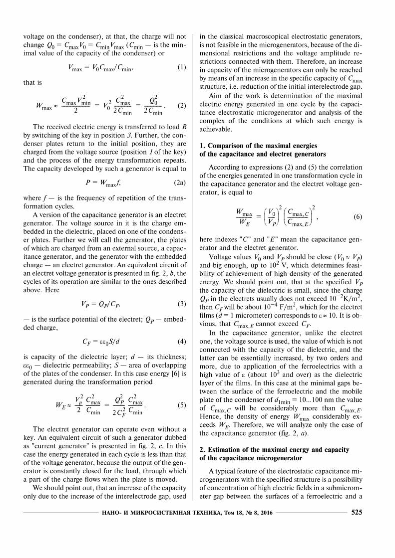
НАНО- И МИКРОСИСТЕМНАЯ ТЕХНИКА, Том 18, № 8, 2016 525
voltage on the condenser), at that, the charge will notchange Q0 = CmaxV0 = CminVmax (Cmin � is the min-imal value of the capacity of the condenser) or
Vmax = V0Cmax/Cmin, (1)
that is
Wmax ≈ = = . (2)
The received electric energy is transferred to load Rby switching of the key in position 3. Further, the con-denser plates return to the initial position, they arecharged from the voltage source (position 1 of the key)and the process of the energy transformation repeats.The capacity developed by such a generator is equal to
P = Wmax f, (2а)
where f � is the frequency of repetition of the trans-formation cycles.
A version of the capacitance generator is an electretgenerator. The voltage source in it is the charge em-bedded in the dielectric, placed on one of the condens-er plates. Further we will call the generator, the platesof which are charged from an external source, a capac-itance generator, and the generator with the embeddedcharge � an electret generator. An equivalent circuit ofan electret voltage generator is presented in fig. 2, b, thecycles of its operation are similar to the ones describedabove. Here
VP = QP/CF, (3)
� is the surface potential of the electret; QP � embed-ded charge,
CF = εε0S/d (4)
is capacity of the dielectric layer; d � its thickness;εε0 � dielectric permeability; S � area of overlappingof the plates of the condenser. In this case energy [6] isgenerated during the transformation period
WE ≈ = . (5)
The electret generator can operate even without akey. An equivalent circuit of such a generator dubbedas "current generator" is presented in fig. 2, c. In thiscase the energy generated in each cycle is less than thatof the voltage generator, because the output of the gen-erator is constantly closed for the load, through whicha part of the charge flows when the plate is moved.
We should point out, that an increase of the capacityonly due to the increase of the interelectrode gap, used
in the classical macroscopical electrostatic generators,is not feasible in the microgenerators, because of the di-mensional restrictions and the voltage amplitude re-strictions connected with them. Therefore, an increasein capacity of the microgenerators can only be reachedby means of an increase in the specific capacity of Cmaxstructure, i.e. reduction of the initial interelectrode gap.
Aim of the work is determination of the maximalelectric energy generated in one cycle by the capaci-tance electrostatic microgenerator and analysis of thecomplex of the conditions at which such energy isachievable.
1. Comparison of the maximal energiesof the capacitance and electret generators
According to expressions (2) and (5) the correlationof the energies generated in one transformation cycle inthe capacitance generator and the electret voltage gen-erator, is equal to
= , (6)
here indexes "C " and "E " mean the capacitance gen-erator and the electret generator.
Voltage values V0 and VP should be close (V0 ≈ VP)and big enough, up to 102 V, which determines feasi-bility of achievement of high density of the generatedenergy. We should point out, that at the specified VPthe capacity of the dielectric is small, since the chargeQP in the electrets usually does not exceed 10�2K/m2,then CF will be about 10�4 F/m2, which for the electretfilms (d = 1 micrometer) corresponds to ε ≈ 10. It is ob-vious, that Cmax,E cannot exceed CF.
In the capacitance generator, unlike the electretone, the voltage source is used, the value of which is notconnected with the capacity of the dielectric, and thelatter can be essentially increased, by two orders andmore, due to application of the ferroelectrics with ahigh value of ε (about 103 and over) as the dielectriclayer of the films. In this case at the minimal gaps be-tween the surface of the ferroelectric and the mobileplate of the condenser of d1min = 10...100 nm the valueof Cmax,C will be considerably more than Cmax,E.Hence, the density of energy Wmax considerably ex-ceeds WE. Therefore, we will analyze only the case ofthe capacitance generator (fig. 2, а).
2. Estimation of the maximal energy and capacityof the capacitance microgenerator
A typical feature of the electrostatic capacitance mi-crogenerators with the specified structure is a possibilityof concentration of high electric fields in a submicrom-eter gap between the surfaces of a ferroelectric and a
CmaxVmin2
2------------------- V0
2 Cmax2
2Cmin------------
Q02
2Cmin------------
Vp2
2-----
Cmax2
Cmin----------
QP2
2CF2
--------Cmax
2
Cmin----------
Wmax
WE-----------
V0
VP-----
⎝ ⎠⎜ ⎟⎛ ⎞
2Cmax,C
Cmax,E--------------
⎝ ⎠⎜ ⎟⎛ ⎞
2
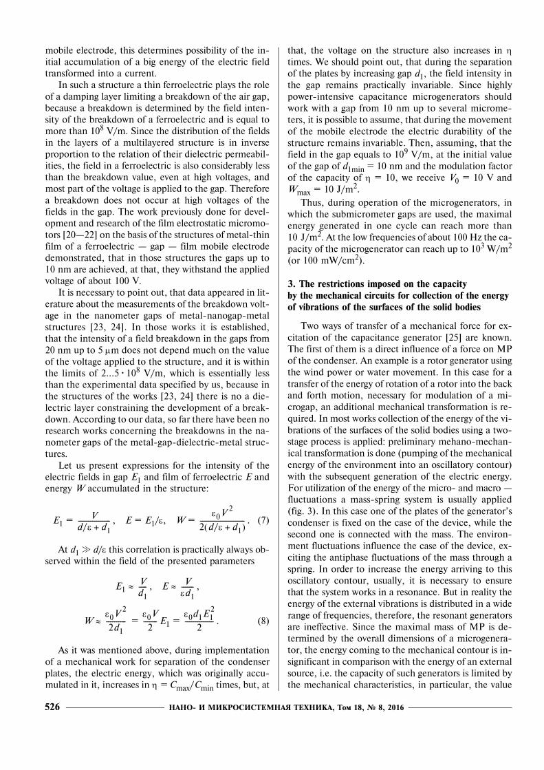
НАНО- И МИКРОСИСТЕМНАЯ ТЕХНИКА, Том 18, № 8, 2016526
mobile electrode, this determines possibility of the in-itial accumulation of a big energy of the electric fieldtransformed into a current.
In such a structure a thin ferroelectric plays the roleof a damping layer limiting a breakdown of the air gap,because a breakdown is determined by the field inten-sity of the breakdown of a ferroelectric and is equal tomore than 108 V/m. Since the distribution of the fieldsin the layers of a multilayered structure is in inverseproportion to the relation of their dielectric permeabil-ities, the field in a ferroelectric is also considerably lessthan the breakdown value, even at high voltages, andmost part of the voltage is applied to the gap. Thereforea breakdown does not occur at high voltages of thefields in the gap. The work previously done for devel-opment and research of the film electrostatic micromo-tors [20�22] on the basis of the structures of metal-thinfilm of a ferroelectric � gap � film mobile electrodedemonstrated, that in those structures the gaps up to10 nm are achieved, at that, they withstand the appliedvoltage of about 100 V.
It is necessary to point out, that data appeared in lit-erature about the measurements of the breakdown volt-age in the nanometer gaps of metal-nanogap-metalstructures [23, 24]. In those works it is established,that the intensity of a field breakdown in the gaps from20 nm up to 5 μm does not depend much on the valueof the voltage applied to the structure, and it is withinthe limits of 2...5�108 V/m, which is essentially lessthan the experimental data specified by us, because inthe structures of the works [23, 24] there is no a die-lectric layer constraining the development of a break-down. According to our data, so far there have been noresearch works concerning the breakdowns in the na-nometer gaps of the metal-gap-dielectric-metal struc-tures.
Let us present expressions for the intensity of theelectric fields in gap E1 and film of ferroelectric E andenergy W accumulated in the structure:
E1 = , E = E1/ε, W = . (7)
At d1 . d/ε this correlation is practically always ob-served within the field of the presented parameters
E1 ≈ , E ≈ ,
W ≈ = E1 = . (8)
As it was mentioned above, during implementationof a mechanical work for separation of the condenserplates, the electric energy, which was originally accu-mulated in it, increases in η = Cmax/Cmin times, but, at
that, the voltage on the structure also increases in ηtimes. We should point out, that during the separationof the plates by increasing gap d1, the field intensity inthe gap remains practically invariable. Since highlypower-intensive capacitance microgenerators shouldwork with a gap from 10 nm up to several microme-ters, it is possible to assume, that during the movementof the mobile electrode the electric durability of thestructure remains invariable. Then, assuming, that thefield in the gap equals to 109 V/m, at the initial valueof the gap of d1min = 10 nm and the modulation factorof the capacity of η = 10, we receive V0 = 10 V andWmax = 10 J/m2.
Thus, during operation of the microgenerators, inwhich the submicrometer gaps are used, the maximalenergy generated in one cycle can reach more than10 J/m2. At the low frequencies of about 100 Hz the ca-pacity of the microgenerator can reach up to 103 W/m2
(or 100 mW/сm2).
3. The restrictions imposed on the capacityby the mechanical circuits for collection of the energy of vibrations of the surfaces of the solid bodies
Two ways of transfer of a mechanical force for ex-citation of the capacitance generator [25] are known.The first of them is a direct influence of a force on MPof the condenser. An example is a rotor generator usingthe wind power or water movement. In this case for atransfer of the energy of rotation of a rotor into the backand forth motion, necessary for modulation of a mi-crogap, an additional mechanical transformation is re-quired. In most works collection of the energy of the vi-brations of the surfaces of the solid bodies using a two-stage process is applied: preliminary mehano-mechan-ical transformation is done (pumping of the mechanicalenergy of the environment into an oscillatory contour)with the subsequent generation of the electric energy.For utilization of the energy of the micro- and macro �fluctuations a mass-spring system is usually applied(fig. 3). In this case one of the plates of the generator�scondenser is fixed on the case of the device, while thesecond one is connected with the mass. The environ-ment fluctuations influence the case of the device, ex-citing the antiphase fluctuations of the mass through aspring. In order to increase the energy arriving to thisoscillatory contour, usually, it is necessary to ensurethat the system works in a resonance. But in reality theenergy of the external vibrations is distributed in a widerange of frequencies, therefore, the resonant generatorsare ineffective. Since the maximal mass of MP is de-termined by the overall dimensions of a microgenera-tor, the energy coming to the mechanical contour is in-significant in comparison with the energy of an externalsource, i.e. the capacity of such generators is limited bythe mechanical characteristics, in particular, the value
Vd/ε d1+----------------
ε0V2
2 d/ε d1+( )----------------------
Vd1---- V
εd1------
ε0V2
2d1----------
ε0V
2-------
ε0d1E12
2--------------
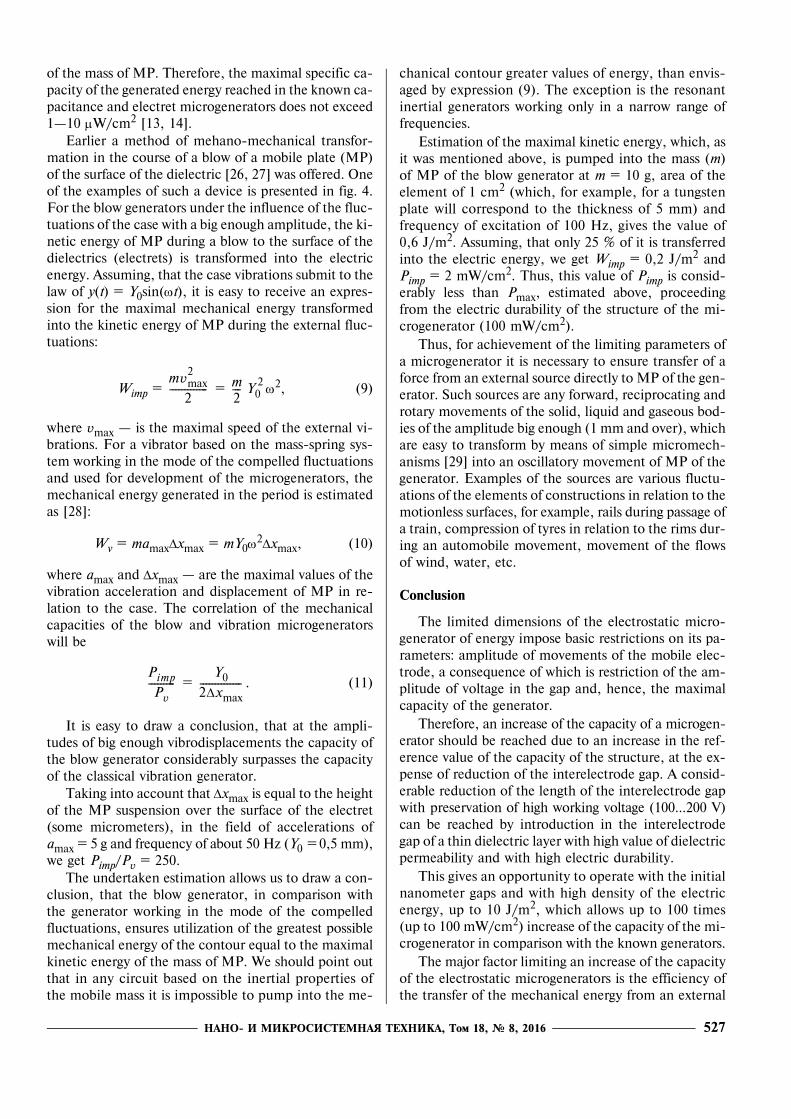
НАНО- И МИКРОСИСТЕМНАЯ ТЕХНИКА, Том 18, № 8, 2016 527
of the mass of MP. Therefore, the maximal specific ca-pacity of the generated energy reached in the known ca-pacitance and electret microgenerators does not exceed1�10 μW/сm2 [13, 14].
Earlier a method of mehano-mechanical transfor-mation in the course of a blow of a mobile plate (MP)of the surface of the dielectric [26, 27] was offered. Oneof the examples of such a device is presented in fig. 4.For the blow generators under the influence of the fluc-tuations of the case with a big enough amplitude, the ki-netic energy of MP during a blow to the surface of thedielectrics (electrets) is transformed into the electricenergy. Assuming, that the case vibrations submit to thelaw of y(t) = Y0sin(ωt), it is easy to receive an expres-sion for the maximal mechanical energy transformedinto the kinetic energy of MP during the external fluc-tuations:
Wimp = = ω2, (9)
where vmax � is the maximal speed of the external vi-brations. For a vibrator based on the mass-spring sys-tem working in the mode of the compelled fluctuationsand used for development of the microgenerators, themechanical energy generated in the period is estimatedas [28]:
Wv = mamaxΔxmax = mY0ω2Δxmax, (10)
where amax and Δxmax � are the maximal values of thevibration acceleration and displacement of MP in re-lation to the case. The correlation of the mechanicalcapacities of the blow and vibration microgeneratorswill be
= . (11)
It is easy to draw a conclusion, that at the ampli-tudes of big enough vibrodisplacements the capacity ofthe blow generator considerably surpasses the capacityof the classical vibration generator.
Taking into account that Δxmax is equal to the heightof the MP suspension over the surface of the electret(some micrometers), in the field of accelerations ofamax = 5 g and frequency of about 50 Hz (Y0 = 0,5 mm),we get Pimp/Pv = 250.
The undertaken estimation allows us to draw a con-clusion, that the blow generator, in comparison withthe generator working in the mode of the compelledfluctuations, ensures utilization of the greatest possiblemechanical energy of the contour equal to the maximalkinetic energy of the mass of MP. We should point outthat in any circuit based on the inertial properties ofthe mobile mass it is impossible to pump into the me-
chanical contour greater values of energy, than envis-aged by expression (9). The exception is the resonantinertial generators working only in a narrow range offrequencies.
Estimation of the maximal kinetic energy, which, asit was mentioned above, is pumped into the mass (m)of MP of the blow generator at m = 10 g, area of theelement of 1 cm2 (which, for example, for a tungstenplate will correspond to the thickness of 5 mm) andfrequency of excitation of 100 Hz, gives the value of0,6 J/m2. Assuming, that only 25 % of it is transferredinto the electric energy, we get Wimp = 0,2 J/m2 andPimp = 2 mW/сm2. Thus, this value of Pimp is consid-erably less than Pmax, estimated above, proceedingfrom the electric durability of the structure of the mi-crogenerator (100 mW/сm2).
Thus, for achievement of the limiting parameters ofa microgenerator it is necessary to ensure transfer of aforce from an external source directly to MP of the gen-erator. Such sources are any forward, reciprocating androtary movements of the solid, liquid and gaseous bod-ies of the amplitude big enough (1 mm and over), whichare easy to transform by means of simple micromech-anisms [29] into an oscillatory movement of MP of thegenerator. Examples of the sources are various fluctu-ations of the elements of constructions in relation to themotionless surfaces, for example, rails during passage ofa train, compression of tyres in relation to the rims dur-ing an automobile movement, movement of the flowsof wind, water, etc.
Conclusion
The limited dimensions of the electrostatic micro-generator of energy impose basic restrictions on its pa-rameters: amplitude of movements of the mobile elec-trode, a consequence of which is restriction of the am-plitude of voltage in the gap and, hence, the maximalcapacity of the generator.
Therefore, an increase of the capacity of a microgen-erator should be reached due to an increase in the ref-erence value of the capacity of the structure, at the ex-pense of reduction of the interelectrode gap. A consid-erable reduction of the length of the interelectrode gapwith preservation of high working voltage (100...200 V)can be reached by introduction in the interelectrodegap of a thin dielectric layer with high value of dielectricpermeability and with high electric durability.
This gives an opportunity to operate with the initialnanometer gaps and with high density of the electricenergy, up to 10 J/m2, which allows up to 100 times(up to 100 mW/сm2) increase of the capacity of the mi-crogenerator in comparison with the known generators.
The major factor limiting an increase of the capacityof the electrostatic microgenerators is the efficiency ofthe transfer of the mechanical energy from an external
mvmax2
2------------- m
2--- Y0
2
Pimp
Pv---------
Y0
2Δxmax--------------
НАНО- И МИКРОСИСТЕМНАЯ ТЕХНИКА, Том 18, № 8, 2016528
source to the mobile element of the generator. For a ca-pacity increase it is necessary to change the way of ap-plication of the force from an external source to themobile plate of the condenser of the generator, because,according to estimates, in the widely applied circuits oftransformation using the inertial properties of mass ofMP, the developed force does not allow to reach a highdensity of the generated energy.
For a capacity increase it is necessary to use the me-chanical designs of the generator, which ensure a directapplication of a force from a source of external move-ment to the mobile plate of the generator.
References
1. Roundy S., Wright P. K., Rabaey J. A Study of low levelvibrations as a power source for wireless sensor nodes, Comput.Commun., 2003, vol. 26, no. 11, pp. 1131�1144.
2. Mitcheson P. D., Miao P., Stark B. H. et al. MEMSelectrostatic micropower generator for low frequency operation,Sensors and Actuators, 2004, vol. 115, no. 2�3, pp. 523�529.
3. Cook-Chennault K. A., Thambi N., Sastry A. M. Power-ing MEMS portable devices � a review of non-regenerative andregenerative power supply systems with special emphasis on pi-ezoelectric energy harvesting systems, Smart Mater. Struct., 2008,vol. 17, pp. 043001 (33 pp.)
4. Cepnik C., Lausecker R., Wallrabe U. Review on electro-dynamic energy harvesters � a classification approach, Microma-chines, 2013, vol. 4, pp. 168�196.
5. Caliт R., Rongala U. B., Camboni D. et al. Piezoelectricenergy harvesting solutions, Sensors, 2014, vol. 14, pp. 4755�4790.
6. Moore A. D., Ed., Electrostatics and Its Application, Wiley,New York, 1973.
7. Basset P., Marty F., Dudka A. et al. A bath fabricated andelectret-free silicon electrostatic vibration energy harvester,J. Mictomech. Microeng., 2009, vol. 19, pp. 115025 (12 pp.)
8. Hoffmann D., Folkmer B., Manoli Y. Fabrication, char-acterization and modelling of electrostatic micro-generators,J. Micromech. Microeng., 2009, vol. 19, pp. 094001 (11 pp.)
9. Roundy S., Wright P. K., Pister K. S. J. Micro-electro-static vibration-to-electricity converters, Proc. IMECE, Novem-ber 17�22: New Orleans, Louisiana, 2002, pp. 1�10.
10. Naruse Y. Matsubara N., Mabuchi K. et al. Electrostaticmicro power generation from low-frequency vibration such ashuman motion, J. Micromech. Microeng., 2009, vol. 19, pp. 094002(5 pp.).
11. Masaki T., Sakurai K., Yokoyama T. et al. Power outputenhancement of a vibration-driven electret generator for wirelesssensor applications, J. Micromech. Microeng., 2011, vol. 21,pp. 104004 (5 pp.)
12. Suzuki Y. Recent progress in MEMS electret generator forenergy harvesting, IEEJ Trans., 2011, vol. 6, pp. 101�111.
13. Okamoto H., Suzuki T., Mori K. et al. The advantagesand potential of electret-based vibration-driven micro energyharvesters, Int. J. Energy Res., 2009, vol. 33, pp. 1180�1190.
14. Grachevski S. M., Funkenbush P. D., Jia Z. et al. Designand modeling of a micro-energy harvester using embedded chargelayer, J. Micromech. Microeng., 2006, vol. 16, pp. 235�241.
15. Mizuno M., Chetwynd P. G. Investigation of resonancemicrogenerator, J. Micromech. Microeng., 2003, vol. 13,pp. 209�216.
16. Guillemet R., Basset P., Galayko D. et al. Design opti-mization of an out-of-plane gap-closing electrostatic vibrationenergy harvester (VEH) with a limitation on the output voltage,Analog Integr. Circ. Sig. Process, 2012, vol. 71, pp. 39�47.
17. Miao P., Holmes A. S., Yeatman E. M. et al. Micro-ma-chined variable capacitors for power generation, Electrostatics2003, Taylor & Francis Group, LLC, 2004, pp. 53�58.
18. Wang F., Hansen O. Electrostatic energy harvesting de-vice with out-of-the-plane gap closing scheme, Proc. of Transduc-ers 2013, Barcelona, SPAIN, 16�20 June 2013, pp. 2237�2240.
19. Miao P., Mitcheson P. D., Holmes A. S. et al. MEMSinertial power generators for biomedical applications, Microsys-tem Technologies, 2006, vol. 12, pp. 1079�1083.
20. Baginsky I. L., Kostsov E. G. High-energy capacitiveelectrostatic micromotors, J. Micromech. Microeng., 2003, vol. 13,no. 2, pp. 190�200.
21. Baginsky I. L., Kostsov E. G. Electrostatic micromotorbased on ferroelectric ceramics, J. Micromech. Microeng., 2004,vol. 14, no. 11, pp. 1569�1575.
22. Baginsky I. L., Kostsov E. G. High energy output MEMSbased on thin layers of ferroelectric materials, Ferroelectrics,2007, vol. 351, pp. 69�78.
23. Babrauskas V. Arc breakdown in air over very small gapdistances, Proc. 13th international conference INTERFLAM 2013,Greenwich, London, UK.
24. Meng G., Cheng Y., Chen L. et al. Discharge behaviorsof electrical breakdown across nanometer vacuum gaps, 2013IEEE International Conference on Solid Dielectrics, Bologna, Italy,June 30 � July 4, 2013, pp. 662�665.
25. Stephen N. G. On energy harvesting from ambient vibra-tion, J. Sound Vibration, 2006, vol. 293, pp. 409�425.
26. Baginsky I. L., Kostsov E. G., Sokolov A. A. New ap-proach to the development of impact-type electrostatic micro-generators, Optoelectronics, Instrumentation and Data Processing,2015, vol. 51, no. 3, pp. 310�320.
27. Baginsky I., Kostsov E., Sokolov A. Single-capacitor elec-tret impact microgenerator, Micromachines, 2016, vol. 7, no. 1,5, 11 pp.
28. Yeatman E. M., Mitcheson P. D., Holmes A. S. Micro-engineered devices for motion energy harvesting, Proc. IEEEInternational Electron Devices Meeting, Washington, DC, USA,10�12 December 2007, pp. 375�378.
29. Pham P. H., Dao D. V., Sugiyama S. A micro transpor-tation system (MTS) with large movement of containers drivenby electrostatic comb-drive actuators, J. Micromech. Microeng.,2007, vol. 17, pp. 2125�2131.
Аäpес pеäакöии жуpнаëа: 107076, Москва, Стpоìынский пеp., 4. Теëефон pеäакöии жуpнаëа (499) 269-5510. E-mail: [email protected]Жуpнаë заpеãистpиpован в Феäераëüной сëужбе по наäзору за собëþäениеì законоäатеëüства в сфере ìассовых коììуникаöий и охране куëüтурноãо насëеäия.
Свиäетеëüство о pеãистpаöии ПИ № 77-18289 от 06.09.04.
Техни÷еский pеäактоp Т. А. Шацкая. Коppектоp Т. В. Пчелкина.
Сäано в набоp 21.06.2016. Поäписано в пе÷атü 22.07.2016. Фоpìат 60Ѕ88 1/8. Заказ МС0816. Цена äоãоворнаяОриãинаë-ìакет ООО «Аäвансеä соëþøнз». Отпе÷атано в ООО «Аäвансеä соëþøнз». 119071, ã. Москва, Ленинский пр-т, ä. 19, стр. 1. Сайт: www.aov.ru


