Embed Size (px)
Citation preview
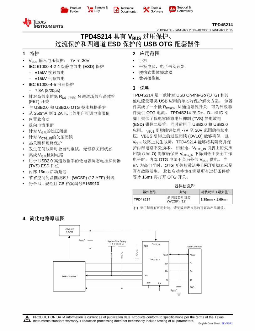
OTG 5 VSource
COTG*
USB Controller
ADJ
VOTG_IN
VBUS
D+
D–
ID
DET
FLT EN
GND
CBUS*
VBUS
D+
D–
ID
TPD4S214
USB Connector
System Side Supply(1.8 V to 3.6 V)
Product
Folder
Sample &Buy
Technical
Documents
Tools &
Software
Support &Community
TPD4S214ZHCSAT5F –JANUARY 2013–REVISED JANUARY 2015
TPD4S214 具具有有 VBUS 过过压压保保护护、、过过流流保保护护和和四四通通道道 ESD 保保护护的的 USB OTG 配配套套器器件件
1 特特性性 2 应应用用范范围围
1• VBUS 输入电压保护:–7V 至 30V • 手机
• IEC 61000-4-2 4 级静电放电 (ESD) 保护 • 平板电脑,电子书阅读器
• 便携式媒体播放器– ±15kV 接触放电
• 数码摄像机– ±15kV 气隙放电
• IEC 61000-4-5 浪涌保护3 说说明明– 7.8A (8/20μs)TPD4S214 是一款针对 USB On-the-Go (OTG) 和其• 针对高效率的低 RDS(导通)N 通道场效应晶体管他电流受限类 USB 应用的单芯片保护解决方案。 该器(FET) 开关
件集成了一个低 RDS(ON) N 通道限流开关,可为外设器• 与 USB2.0 和 USB3.0 OTG 技术规格兼容
件提供 OTG 电流。 TPD4S214 在 D+、D– 和 ID 引• 从 250mA 到 1.2A 以上的用户可调电流限值脚上提供了低电容瞬态电压抑制 (TVS) 静电放电• 内置软启动(ESD) 钳位二极管,同时适用于 USB2.0 和 USB3.0• 反向电流阻断应用。 VBUS 引脚能够处理 -7V 至 30V 范围的持续电• 针对 V总线的过压闭锁压。VBUS 引脚上的过压闭锁 (OVLO) 能够确保一旦• 针对 VOTG_IN的欠压闭锁VBUS 线路上发生故障,TPD4S214 能够将其隔离并保• 热关断和短路保护护内部电路不受损坏。 相似地,VOTG_IN 引脚上的欠压• 发生任何故障时会自动重试;无锁存关闭状态闭锁 (UVLO) 能够确保在 VOTG_IN 下降到低于安全工作• 集成 V总线检测电路电平时,内部 OTG 电源不会为外部 VBUS 供电。 当• 用于 USB2.0 高速数据率的低电容瞬态电压抑制器EN 为高电平时,OTG 开关被激活并且FLT引脚表示是(TVS) ESD 钳位
否有故障发生。 此软启动特性在满足所有运行条件后• 内部 16ms 启动延迟
等待 16ms 再打开 OTG 开关。• 节省空间的晶圆级芯片 (WCSP) (12-YFF) 封装
• 符合 UL 规范且 CB 档案编号E169910器器件件信信息息(1)
器器件件型型号号 封封装装 封封装装尺尺寸寸((最最大大值值))
晶圆级芯片封装TPD4S214 1.39mm x 1.69mm(WCSP) (12)
(1) 要了解所有可用封装,请见数据表末尾的可订购产品附录。
4 简简化化电电路路原原理理图图
1
PRODUCTION DATA information is current as of publication date. Products conform to specifications per the terms of the TexasInstruments standard warranty. Production processing does not necessarily include testing of all parameters.
English Data Sheet: SLVSBR1
TPD4S214ZHCSAT5F –JANUARY 2013–REVISED JANUARY 2015 www.ti.com.cn
目目录录
7.12 Typical Characteristics ............................................ 81 特特性性.......................................................................... 18 Detailed Description ............................................ 112 应应用用范范围围................................................................... 1
8.1 Overview ................................................................. 113 说说明明.......................................................................... 18.2 Functional Block Diagram ....................................... 114 简简化化电电路路原原理理图图........................................................ 18.3 Feature Description................................................. 125 修修订订历历史史记记录录 ........................................................... 28.4 Device Functional Modes........................................ 176 Pin Configuration and Functions ......................... 3
9 Application and Implementation ........................ 187 Specifications......................................................... 49.1 Application Information............................................ 187.1 Absolute Maximum Ratings ...................................... 49.2 Typical Application ................................................. 187.2 ESD Ratings ............................................................ 4
10 Power Supply Recommendations ..................... 227.3 Recommended Operating Conditions....................... 411 Layout................................................................... 227.4 Thermal Information .................................................. 5
11.1 Layout Guidelines ................................................. 227.5 Thermal Shutdown.................................................... 511.2 Layout Example .................................................... 227.6 Electrical Characteristics for EN, FLT, DET, D+, D–,
VBUS, ID Pins ............................................................. 5 12 器器件件和和文文档档支支持持 ..................................................... 237.7 Electrical characteristics for UVLO / OVLO .............. 6 12.1 文档支持 ................................................................ 237.8 Electrical Characteristics for DET Circuits ................ 6 12.2 商标 ....................................................................... 237.9 Electrical Characteristics for OTG Switch................. 6 12.3 静电放电警告......................................................... 237.10 Electrical Characteristics for Current Limit and Short 12.4 术语表 ................................................................... 23
Circuit Protection........................................................ 7 13 机机械械封封装装和和可可订订购购信信息息 .......................................... 237.11 Supply Current Consumption.................................. 7
5 修修订订历历史史记记录录
Changes from Revision E (January 2015) to Revision F Page
• 已添加 UL 和 CB 认证。 ........................................................................................................................................................ 1
Changes from Revision D (October 2014) to Revision E Page
• Added RLOAD TEST CONDITIONS to IOCP in the Electrical Characteristics for Current Limit and Short CircuitProtection table. ..................................................................................................................................................................... 7
Changes from Revision C (August 2013) to Revision D Page
• 处理额定值表,特性描述部分,器件功能模式,应用和实施部分,电源相关建议部分,布局部分,器件和文档支持部分以及机械、封装和可订购信息部分。 .................................................................................................................................. 1
Changes from Original (January 2013) to Revision A Page
• 已更改产品预览数据表 ............................................................................................................................................................ 1
Changes from Revision A (February 2013) to Revision B Page
• 已将器件状态从:产品预览更改为:量产数据 ........................................................................................................................ 1
Changes from Revision B (February 2013) to Revision C Page
• YFF PACKAGE Changed the YFF package dimensions ....................................................................................................... 3
2 版权 © 2013–2015, Texas Instruments Incorporated
1.39 mm
1.69
mm
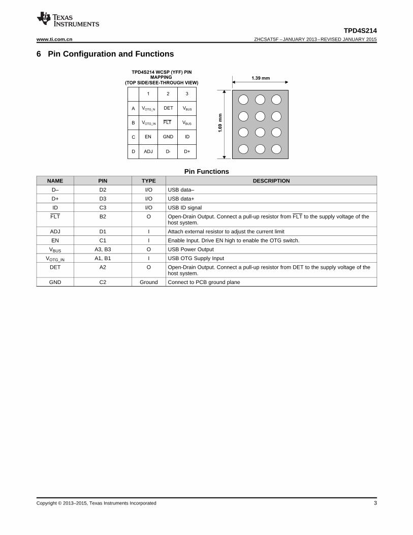
TPD4S214 WCSP (YFF) PINMAPPING
(TOP SIDE/SEE-THROUGH VIEW)
A
B
C
D
VOTG_N
VOTG_IN
EN
ADJ
DET
FLT
GND
D-
VBUS
VBUS
ID
D+
1 2 3
TPD4S214www.ti.com.cn ZHCSAT5F –JANUARY 2013–REVISED JANUARY 2015
6 Pin Configuration and Functions
Pin FunctionsNAME PIN TYPE DESCRIPTION
D– D2 I/O USB data–D+ D3 I/O USB data+ID C3 I/O USB ID signal
FLT B2 O Open-Drain Output. Connect a pull-up resistor from FLT to the supply voltage of thehost system.
ADJ D1 I Attach external resistor to adjust the current limitEN C1 I Enable Input. Drive EN high to enable the OTG switch.
VBUS A3, B3 O USB Power OutputVOTG_IN A1, B1 I USB OTG Supply Input
DET A2 O Open-Drain Output. Connect a pull-up resistor from DET to the supply voltage of thehost system.
GND C2 Ground Connect to PCB ground plane
Copyright © 2013–2015, Texas Instruments Incorporated 3
TPD4S214ZHCSAT5F –JANUARY 2013–REVISED JANUARY 2015 www.ti.com.cn
7 Specifications
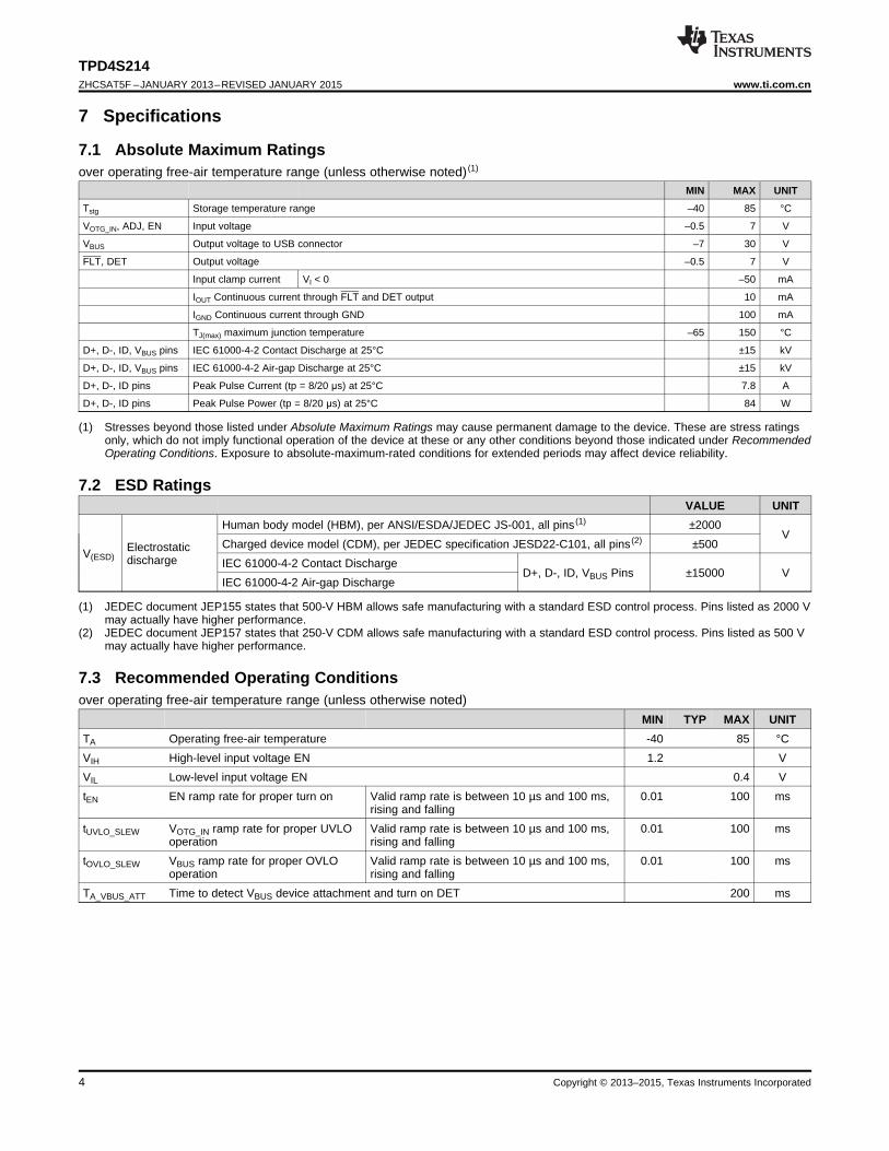
7.1 Absolute Maximum Ratingsover operating free-air temperature range (unless otherwise noted) (1)
MIN MAX UNIT
Tstg Storage temperature range –40 85 °C
VOTG_IN, ADJ, EN Input voltage –0.5 7 V
VBUS Output voltage to USB connector –7 30 V
FLT, DET Output voltage –0.5 7 V
Input clamp current VI < 0 –50 mA
IOUT Continuous current through FLT and DET output 10 mA
IGND Continuous current through GND 100 mA
TJ(max) maximum junction temperature –65 150 °C
D+, D-, ID, VBUS pins IEC 61000-4-2 Contact Discharge at 25°C ±15 kV
D+, D-, ID, VBUS pins IEC 61000-4-2 Air-gap Discharge at 25°C ±15 kV
D+, D-, ID pins Peak Pulse Current (tp = 8/20 μs) at 25°C 7.8 A
D+, D-, ID pins Peak Pulse Power (tp = 8/20 μs) at 25°C 84 W
(1) Stresses beyond those listed under Absolute Maximum Ratings may cause permanent damage to the device. These are stress ratingsonly, which do not imply functional operation of the device at these or any other conditions beyond those indicated under RecommendedOperating Conditions. Exposure to absolute-maximum-rated conditions for extended periods may affect device reliability.
7.2 ESD RatingsVALUE UNIT
Human body model (HBM), per ANSI/ESDA/JEDEC JS-001, all pins (1) ±2000V
Charged device model (CDM), per JEDEC specification JESD22-C101, all pins (2) ±500ElectrostaticV(ESD) discharge IEC 61000-4-2 Contact DischargeD+, D-, ID, VBUS Pins ±15000 V
IEC 61000-4-2 Air-gap Discharge
(1) JEDEC document JEP155 states that 500-V HBM allows safe manufacturing with a standard ESD control process. Pins listed as 2000 Vmay actually have higher performance.
(2) JEDEC document JEP157 states that 250-V CDM allows safe manufacturing with a standard ESD control process. Pins listed as 500 Vmay actually have higher performance.
7.3 Recommended Operating Conditionsover operating free-air temperature range (unless otherwise noted)
MIN TYP MAX UNITTA Operating free-air temperature -40 85 °CVIH High-level input voltage EN 1.2 VVIL Low-level input voltage EN 0.4 VtEN EN ramp rate for proper turn on Valid ramp rate is between 10 µs and 100 ms, 0.01 100 ms
rising and fallingtUVLO_SLEW VOTG_IN ramp rate for proper UVLO Valid ramp rate is between 10 µs and 100 ms, 0.01 100 ms
operation rising and fallingtOVLO_SLEW VBUS ramp rate for proper OVLO Valid ramp rate is between 10 µs and 100 ms, 0.01 100 ms
operation rising and fallingTA_VBUS_ATT Time to detect VBUS device attachment and turn on DET 200 ms
4 Copyright © 2013–2015, Texas Instruments Incorporated
TPD4S214www.ti.com.cn ZHCSAT5F –JANUARY 2013–REVISED JANUARY 2015
7.4 Thermal InformationTPD4S214
THERMAL METRIC (1) YFF UNIT12 PINS
RθJA Junction-to-ambient thermal resistance 89.1RθJC(top) Junction-to-case (top) thermal resistance 0.5RθJB Junction-to-board thermal resistance 40.0 °C/WψJT Junction-to-top characterization parameter 3.0ψJB Junction-to-board characterization parameter 39.0
(1) For more information about traditional and new thermal metrics, see the IC Package Thermal Metrics application report, SPRA953.
7.5 Thermal Shutdownover operating free-air temperature range (unless otherwise noted)
PARAMETER TEST CONDITIONS TYP MAX UNITTSHDN+ Shutdown temp rising 141 ºCTSHDN– Shutdown temp falling 125 ºCTHYST Thermal-shutdown Hysteresis 16 ºCPMAX Maximum power dissipation 0.16 W
VOTG_IN = 5 V, Rload = 5 Ω, EN = 5 V, RADJ = 75 KΩTJMAX Junction Temp at max power dissipation 150 ºC
7.6 Electrical Characteristics for EN, FLT, DET, D+, D–, VBUS, ID Pinsover operating free-air temperature range (unless otherwise noted)
PARAMETER TEST CONDITIONS MIN TYP MAX UNIT
IIL_EN EN pin input leakage current EN = 3.3 V 1 µA
IOL FLT, DET pin output leakage current FLT, DET = 3.6 V 1 µA
VOL_FLT Low-level output voltage FLT VBUS or VOTG_IN = 5 V or 0 V IOL = 100 µA 100 mV
VOL_DET Low-level output voltage DET VBUS and VOTG_IN = 5 V or 0 V IOL = 100 µA 100 mV
CEN Enable capacitance VBIAS = 1.8 V, f = 1 MHz, 30 mVpp ripple, VOTG_IN = 5 V 4.5 pF
Diode forward voltage D+, D–, ID pins; lowerVD IO = 8 mA 0.95 Vclamp diode
IL_D Leakage current on D+, D–, ID Pins D+, D–, ID = 3.3 V 100 nA
Differential capacitance between the D+, D–ΔCIO VBIAS = 1.8 V, f = 1 MHz, 30 mVpp ripple, VOTG_IN = 5 V 0.04 pFlines
Capacitance to GND for the D+, D– lines 1.9CIO VBIAS = 1.8 V, f = 1 MHz, 30 mVpp ripple, VOTG_IN = 5 V pF
Capacitance to GND for the ID lines 1.9
Breakdown voltage D+, D–, ID pins Ibr = 1 mA 6 VVBR
Breakdown voltage on VBUS Ibr = 1 mA 33 V
RDYN Dynamic on resistance D+, D–, ID clamps 1 Ω
Copyright © 2013–2015, Texas Instruments Incorporated 5
TPD4S214ZHCSAT5F –JANUARY 2013–REVISED JANUARY 2015 www.ti.com.cn
7.7 Electrical characteristics for UVLO / OVLOover operating free-air temperature range (unless otherwise noted)
PARAMETER TEST CONDITIONS MIN TYP MAX UNIT
INPUT UNDER-VOLTAGE LOCKOUT
Under-voltage lock-out, input power detected VOTG_IN increasing from 0 V to 5 V, No load on VBUSVUVLO+ 3.4 3.6 3.8 Vthreshold rising pin
Under-voltage lock-out, input power detected VOTG_IN decreasing from 5 V to 0 V, No load on VBUSVUVLO– 3.0 3.2 3.5 Vthreshold falling pin
VHYS-UVLO Hysteresis on UVLO Δ of VUVLO+ and VUVLO– 260 mV
VOTG_IN increasing from 0V to 5V, No load on VBUS pin;TRUVLO Recovery time from UVLO 18 mstime from VOTG_IN = VUVLO+ to FLT toggles high
VOTG_IN decreasing from 5V to 0V, No load on VBUSpin;TRESP_UVLO Response time for UVLO 0.18 µstime from VOTG_IN = VUVLO– to FLT toggles low
OUTPUT OVERVOLTAGE LOCKOUT
VOVP+ OVLO rising threshold Both VOTG_IN and VBUS increasing from 5 V to 7 V 5.55 6.15 6.45 V
VOVP– OVLO falling threshold Both VOTG_IN and VBUS decreasing from 7 V to 5 V 5.4 6 6.3 V
VHYS-OVP Hysteresis on OVLO Δ of VUVLO+ and VUVLO– 100 mV
Both VOTG_IN and VBUS decreasing from 7 V to 5 V,VOTG_IN = 5 V;TROVLO Recovery time from OVLO 9 mstime from VBUS = VOVP– to FLT toggles high
Both VOTG_IN and VBUS increasing from 5 V to 7 V,VOTG_IN = 5 V;TRESP_OVLO Response time for OVLO 17 µstime from VBUS = VOVP+ to FLT toggles low
7.8 Electrical Characteristics for DET Circuitsover operating free-air temperature range (unless otherwise noted)
PARAMETER TEST CONDITIONS MIN TYP MAX UNIT
VBUS_VALID– Valid VBUS voltage detect VBUS = 7 V to 0 V 2.7 2.9 3 V
VBUS_VALID+ Valid VBUS voltage detect VBUS = 0 V to 7 V 5.3 5.4 5.6 V
VBUS 0 V to 4 V, 200 ns ramp; VBUS = VBUS_VALID– MIN to DET togglesTDET_DELAY– VBUS detect propagation delay– 4.9 µshigh
VBUS 6 V to 4 V, 200 ns ramp; VBUS = VBUS_VALID+ MAX to DET togglesTDET_DELAY+ VBUS detect propagation delay+ 1.8 µslow
7.9 Electrical Characteristics for OTG Switchover operating free-air temperature range (unless otherwise noted)
PARAMETER TEST CONDITIONS MIN TYP MAX UNIT
RDS_ON OTG switch resistance TA = 25 °C, VBUS = 5 V, IOUT = 100 mA, RADJ = 75 kΩ (1) 263 290 mΩ
VDROP OTG switch voltage drop VBUS = 5 V, IOUT = 100 mA, RADJ = 75 kΩ 12.6 29 mV
VBUS = 30 V, EN = 5 V, VOTG_IN = 5 V 6 µAIOTG_OFF_30V Leakage current at 30V
VBUS = 30 V, EN = 5 V, VOTG_IN = 0 V 11 nA
IOTG_OFF_2V Leakage current at–2V VBUS = -2 V, EN = 5 V, VOTG_IN = 5 V 30 µA
Measured at VOTG_IN VBUS = 0 V, EN = 0 V, VOTG_IN = 5 V 32 µAIOTG_OFF Standby Leakage current
VBUS = 5 V, EN = 0 V, VOTG_IN = 0 V 10 nA
VBUS = 5 V, EN = 5 V, VOTG_IN = 0V 1 nAIBUS_REV Reverse Leakage current
VBUS = 5.5 V, EN = 5 V, VOTG_IN = 5 V 6 µA
TON Turn-ON time RL = 100 Ω, CL = 1 µF, RADJ = 75 kΩ 16 ms
TOFF_EN Turn-OFF time RL = 100 Ω, CL = 1 µF, RADJ = 75 kΩ, toggle EN 80 µs
TOFF_OTG Turn-OFF time RL = 100 Ω, CL = 1 µF, RADJ = 75 kΩ, toggle VOTG_IN 0.5 µs
TRISE Output rise time RL = 100 Ω, CL = 1 µF, RADJ = 75 kΩ 137 µs
TFALL Output fall time RL = 100 Ω, CL = 1 µF, RADJ = 75 kΩ 1.6 µs
(1) RDS(ON) is measured at 25°C
6 Copyright © 2013–2015, Texas Instruments Incorporated
TPD4S214www.ti.com.cn ZHCSAT5F –JANUARY 2013–REVISED JANUARY 2015
7.10 Electrical Characteristics for Current Limit and Short Circuit Protectionover operating free-air temperature range (unless otherwise noted)
PARAMETER TEST CONDITIONS MIN TYP MAX UNIT
RADJ = 226 kΩ (1) 235 245 281Current−limit threshold (maximum RADJ = 75 kΩ (1) 735 792 830
IOCP DC output current IOUT delivered to VOTG_IN = 5 V, RLOAD = 2.0 Ω mARADJ = 62 kΩ (1) 885 959 1005load)RADJ = 45 kΩ (1) 1128 1200 1363
RL = 1 Ω, CL = 1 µF,TBLANK Blanking time after enable VOTG_IN = 5 V 4 msRADJ = 75 kΩ
TDEGL Deglitch time while enabled 9.4 ms
TDET_SC Response time to short circuit 10 µsVOTG_IN = 5 V, RL = 100 Ω,
Hiccup pulse width; auto-retryCL = 1 µF, RADJ = 75 kΩ,TREG Short circuit regulation time 13 mstimeapply short to groundShort circuit over current protectionTOCP Hiccup pulse period 153 mstime
VSHORT Short circuit threshold 4 V
SeeFigure 23 under test RL = 100 Ω, CL = 22 µF, RADJIINRUSH Inrush current during a startup 726 mAconfiguration = 75 kΩ
(1) External resistor tolerance is ±1%
7.11 Supply Current Consumptionover operating free-air temperature range (unless otherwise noted)
PARAMETER TEST CONDITIONS TYP MAX UNIT
RADJ = 75 kΩ 162 200 µAVOTG_IN = 5 V, No load on VBUS,High-level VOTG_IN operating currentIVOTG_INON consumption EN = 5 V RADJ = 226 kΩ 150 200 µA
Copyright © 2013–2015, Texas Instruments Incorporated 7
±0.2 0.0 0.2 0.4 0.6 0.8 1.0 1.2 1.4 1.6 1.8 2.0 2.2 2.4
±0.5 0.0 0.5 1.0 1.5 2.0 2.5 3.0 3.5 4.0 4.5 5.0 5.5 6.0
±20 0 20 40 60 80 100
Cur
rent
(A
)
Vol
tage
(V
)
Time (s)
Votgin Vbus Iotgin
C005
±0.2 0.0 0.2 0.4 0.6 0.8 1.0 1.2 1.4 1.6 1.8 2.0 2.2 2.4
±0.5 0.0 0.5 1.0 1.5 2.0 2.5 3.0 3.5 4.0 4.5 5.0 5.5 6.0
±5 0 5 10 15 20
Cur
rent
(A
)
Vol
tage
(V
)
Time (ms)
Votgin Vbus Iotgin
C006
0.0
0.1
0.2
0.3
0.4
0.5
0.6
0.7
0.8
0.9
1.0
1.1
0.0
0.5
1.0
1.5
2.0
2.5
3.0
3.5
4.0
4.5
5.0
5.5
±15 0 15 30 45 60 75 90 105 120
Cur
rent
(A
)
Vol
tage
(V
)
Time (s)
Votgin Vbus Iotgin
C003
±0.2 0.0 0.2 0.4 0.6 0.8 1.0 1.2 1.4 1.6 1.8 2.0 2.2 2.4
±0.5 0.0 0.5 1.0 1.5 2.0 2.5 3.0 3.5 4.0 4.5 5.0 5.5 6.0
±2 0 2 4 6 8 10 12 14 16
Cur
rent
(A
)
Vol
tage
(V
)
Time (s)
Votgin Vbus Iotgin
C004
0.0
0.2
0.4
0.6
0.8
1.0
1.2
1.4
1.6
1.8
0 50 100 150 200 250 300 350 400
Cur
rent
(A
)
RADJ (k )
±40C
25C
85C
C001
0
50
100
150
200
250
300
350
400
±40 ±20 0 20 40 60 80
Sw
itch
Res
ista
nce
(m
Temperature (C)
250mA
500mA
C002
TPD4S214ZHCSAT5F –JANUARY 2013–REVISED JANUARY 2015 www.ti.com.cn
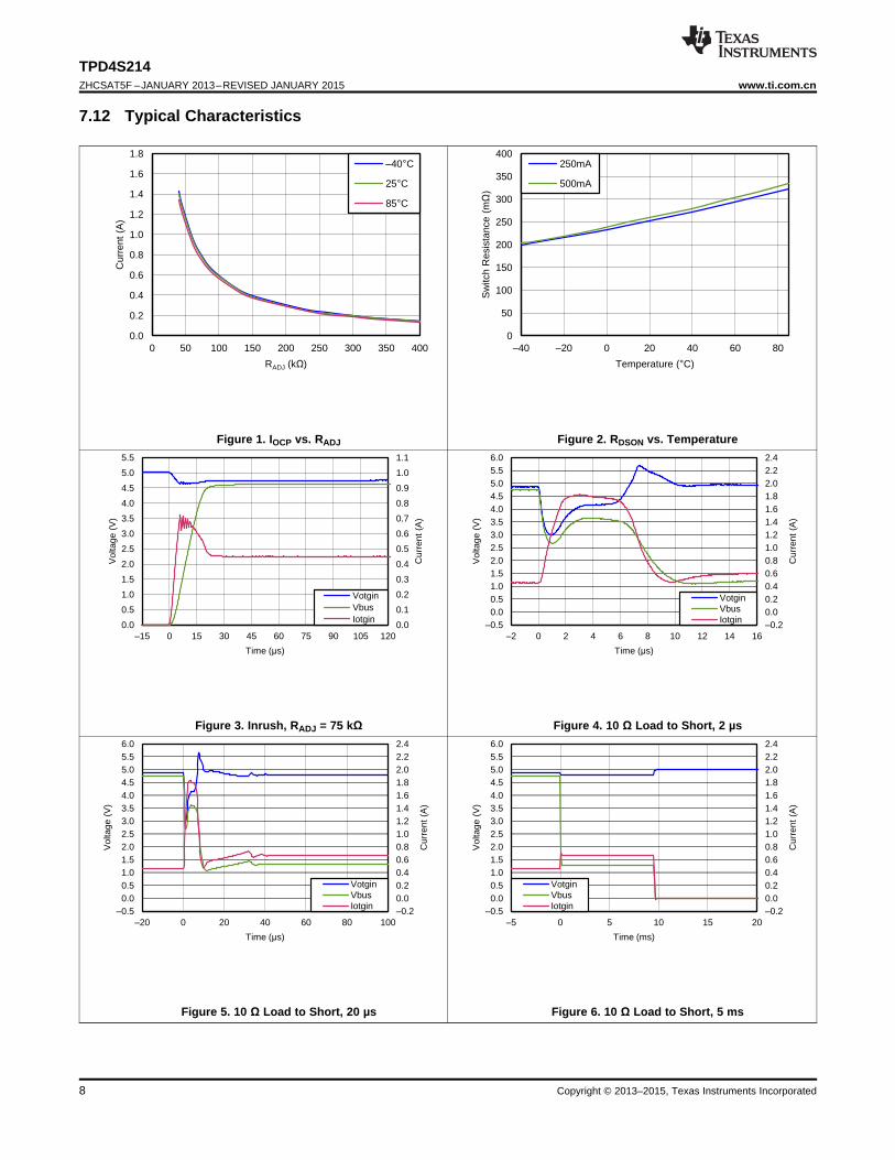
7.12 Typical Characteristics
Figure 1. IOCP vs. RADJ Figure 2. RDSON vs. Temperature
Figure 3. Inrush, RADJ = 75 kΩ Figure 4. 10 Ω Load to Short, 2 µs
Figure 5. 10 Ω Load to Short, 20 µs Figure 6. 10 Ω Load to Short, 5 ms
8 Copyright © 2013–2015, Texas Instruments Incorporated
0.0
0.2
0.4
0.6
0.8
1.0
1.2
1.4
1.6
1.8
2.0
2.2
2.4
0.0 0.5 1.0 1.5 2.0 2.5 3.0 3.5 4.0 4.5 5.0
Cap
acita
nce
(pF
)
VBIAS (V) C011
0
1
2
3
4
5
6
7
±5 0 5 10 15 20 25
Vol
tage
(V
)
Time (ms)
VBUS EN FLT
C012
±20
±10
0
10
20
30
40
50
60
70
±15 0 15 30 45 60 75 90 105 120 135 150 165 180
Vol
tage
(V
)
Time (ns)
ID D+ D±
C009
±70
±60
±50
±40
±30
±20
±10
0
10
20
±15 0 15 30 45 60 75 90 105 120 135 150 165 180
Vol
tage
(V
)
Time (ns)
ID D+ D±
C010
±27
±24
±21
±18
±15
±12
±9
±6
±3
0
3
1M 10M 100M 1G 10G
Gai
n (d
B)
Frequency (Hz) C008
±0.2 0.0 0.2 0.4 0.6 0.8 1.0 1.2 1.4 1.6 1.8 2.0 2.2 2.4
±0.5 0.0 0.5 1.0 1.5 2.0 2.5 3.0 3.5 4.0 4.5 5.0 5.5 6.0
±100 0 100 200 300 400 500
Cur
rent
(A
)
Vol
tage
(V
)
Time (ms)
Votgin Vbus Iotgin
C007
TPD4S214www.ti.com.cn ZHCSAT5F –JANUARY 2013–REVISED JANUARY 2015
Typical Characteristics (continued)
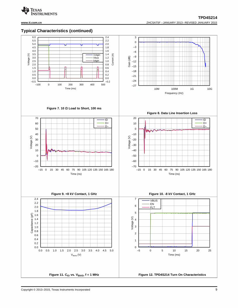
Figure 7. 10 Ω Load to Short, 100 msFigure 8. Data Line Insertion Loss
Figure 9. +8 kV Contact, 1 GHz Figure 10. -8 kV Contact, 1 GHz
Figure 11. CIO vs. VBIAS, f = 1 MHz Figure 12. TPD4S214 Turn On Characteristics
Copyright © 2013–2015, Texas Instruments Incorporated 9
0.0
0.5
1.0
1.5
2.0
2.5
3.0
3.5
0.0 0.5 1.0 1.5 2.0 2.5 3.0 3.5 4.0 4.5
Vol
tage
(V
)
Time (ms)
VBUS
DET
C017
0
1
2
3
4
5
6
7
8
9
10
0 25 50 75 100 125 150 175
Vol
tage
(V
)
Time (ms)
VBUS VOTG FLT
C015
0.0
1.0
2.0
3.0
4.0
5.0
6.0
7.0
8.0
9.0
0.0 0.5 1.0 1.5 2.0 2.5 3.0 3.5 4.0 4.5
Vol
tage
(V
)
Time (ms)
VBUS
DET
C016
0
1
2
3
4
5
6
±25 0 25 50 75 100 125 150 175 200 225
Vol
tage
(V
)
Time (s)
VBUS EN FLT
C013
0
1
2
3
4
5
6
0 10 20 30 40 50 60 70 80
Vol
tage
(V
)
Time (ms)
VBUS VOTG FLT
C014
TPD4S214ZHCSAT5F –JANUARY 2013–REVISED JANUARY 2015 www.ti.com.cn
Typical Characteristics (continued)
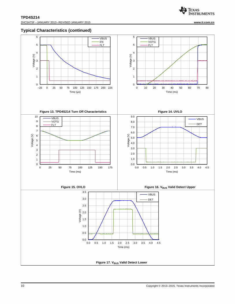
Figure 13. TPD4S214 Turn Off Characteristics Figure 14. UVLO
Figure 15. OVLO Figure 16. VBUS Valid Detect Upper
Figure 17. VBUS Valid Detect Lower
10 Copyright © 2013–2015, Texas Instruments Incorporated
VOTG_IN
InternalBand GapReferance
Current Limiting
OTG Switch
DET
VBUS Detection+
OVLO
VBUS
UVLO
Control Logic+
Charge Pump
ADJ
FLT
EN
GND D+ D– ID
TPD4S214www.ti.com.cn ZHCSAT5F –JANUARY 2013–REVISED JANUARY 2015
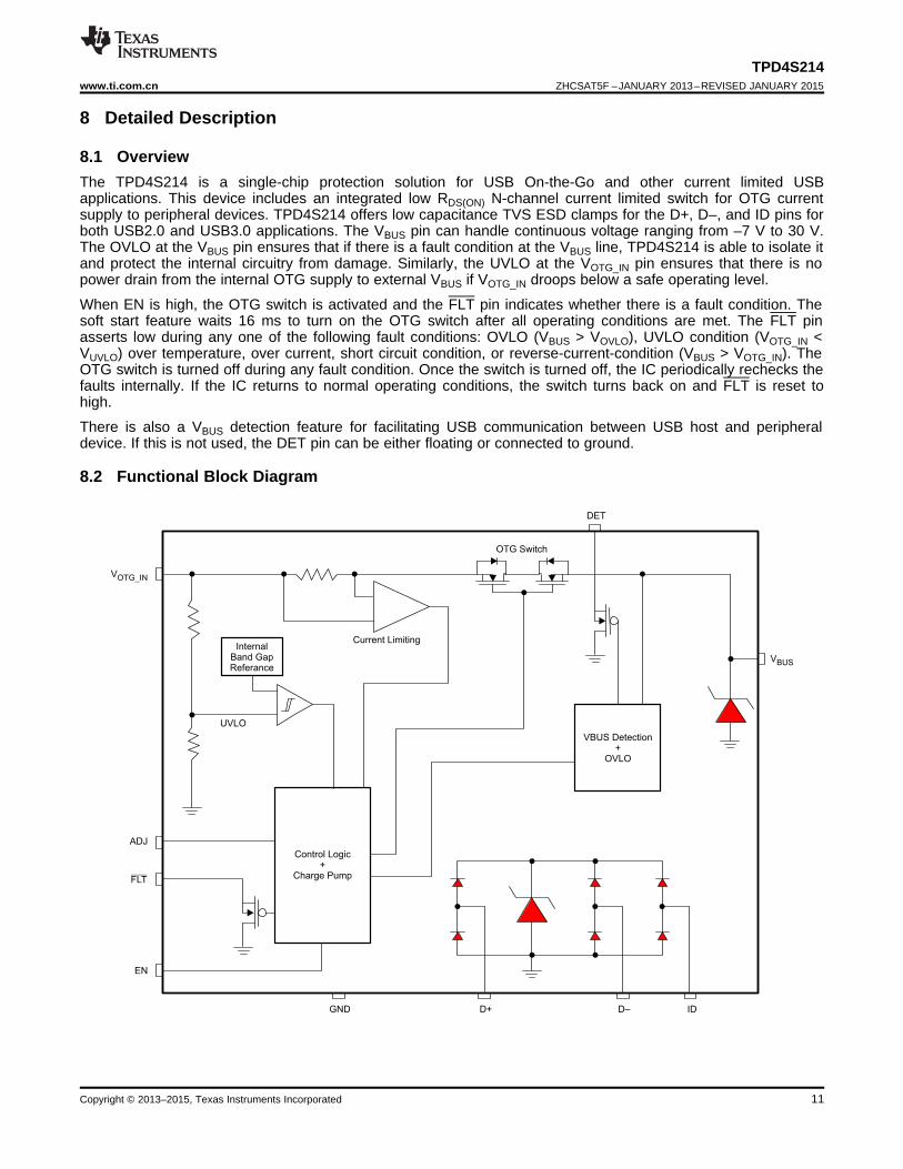
8 Detailed Description
8.1 OverviewThe TPD4S214 is a single-chip protection solution for USB On-the-Go and other current limited USBapplications. This device includes an integrated low RDS(ON) N-channel current limited switch for OTG currentsupply to peripheral devices. TPD4S214 offers low capacitance TVS ESD clamps for the D+, D–, and ID pins forboth USB2.0 and USB3.0 applications. The VBUS pin can handle continuous voltage ranging from –7 V to 30 V.The OVLO at the VBUS pin ensures that if there is a fault condition at the VBUS line, TPD4S214 is able to isolate itand protect the internal circuitry from damage. Similarly, the UVLO at the VOTG_IN pin ensures that there is nopower drain from the internal OTG supply to external VBUS if VOTG_IN droops below a safe operating level.
When EN is high, the OTG switch is activated and the FLT pin indicates whether there is a fault condition. Thesoft start feature waits 16 ms to turn on the OTG switch after all operating conditions are met. The FLT pinasserts low during any one of the following fault conditions: OVLO (VBUS > VOVLO), UVLO condition (VOTG_IN <VUVLO) over temperature, over current, short circuit condition, or reverse-current-condition (VBUS > VOTG_IN). TheOTG switch is turned off during any fault condition. Once the switch is turned off, the IC periodically rechecks thefaults internally. If the IC returns to normal operating conditions, the switch turns back on and FLT is reset tohigh.
There is also a VBUS detection feature for facilitating USB communication between USB host and peripheraldevice. If this is not used, the DET pin can be either floating or connected to ground.
8.2 Functional Block Diagram
Copyright © 2013–2015, Texas Instruments Incorporated 11
TPD4S214ZHCSAT5F –JANUARY 2013–REVISED JANUARY 2015 www.ti.com.cn
8.3 Feature Description
8.3.1 Input Voltage Protection at VBUS from –7 V to 30 VThe VBUS pin can handle continuous voltage ranging from –7 V to 30 V. The OVLO at the VBUS pin ensures that ifthere is a fault condition at the VBUS line, TPD4S214 is able to isolate the fault and protect the internal circuitryfrom damage.
8.3.2 IEC 61000-4-2 Level 4 ESD ProtectionThe I/O pins can withstand ESD events up to ±15-kV contact and air gap. An ESD clamp diverts the current toground.
8.3.3 Low RDS(ON) N-CH FET Switch for High EfficiencyA Low RDS(ON) ensures there is minimal voltage loss when supplying high current to OTG devices.
8.3.4 Compliant with USB2.0 and USB3.0 OTG specThe capability of TPD4S214 to supply greater than 1.2 A of current on VBUS meets or exceeds the USB2.0 andUSB3.0 OTG specification.
8.3.5 User Adjustable Current Limit From 250 mA to Beyond 1.2 AThe designer can select the over current protection level by selecting the proper RADJ.
8.3.6 Built-in Soft-startThe soft start feature waits 16 ms to turn on the OTG switch after all operating conditions are met.
8.3.7 Reverse Current BlockingIf VBUS is greater than VOTG_IN by 50 mV, the OTG switch is disabled in 17.5 ms.
8.3.8 Over Voltage Lock Out for VBUS
OVLO ensures that an over voltage condition on VBUS disables the OTG switch to protect the system.
8.3.9 Under Voltage Lock Out for VOTG_IN
UVLO ensures that an under voltage condition on VBUS disables the OTG switch to protect the system.
8.3.10 Thermal Shutdown and Short Circuit ProtectionTPD4S214 has an over-temperature protection circuit to protect against system faults or improper use. The basicfunction of the thermal shutdown (TSD) circuit is to sense when the junction temperature has exceeded theabsolute maximum rating and shut down the device until the junction temperature has cooled to a safe level.Short circuit protection prevents any damaging current demand from the system.
8.3.11 Auto Retry on any Fault; no Latching off StatesIn any fault condition, TPD4S214 will reassess VBUS, VOTG_IN, and thermal conditions until a safe state is reachedand then enable the OTG switch, eliminating any latched off states.
8.3.12 Integrated VBUS Detection CircuitTPD4S214 has a VBUS detection feature facilitating communication between the USB host and peripheral device.The use of this feature is optional.
8.3.13 Low Capacitance TVS ESD Clamp for USB2.0 High Speed Data RateThe High Speed data lines have a capacitance less than 2 pF, supporting a bandwidth greater than 3 GHz. Thiseasily accommodates the 480-Mbps data rate defined in the USB2.0 specification.
12 Copyright © 2013–2015, Texas Instruments Incorporated
ADJ
OCP
55.358R
I=
TPD4S214
RADJ
ADJ
TPD4S214www.ti.com.cn ZHCSAT5F –JANUARY 2013–REVISED JANUARY 2015
Feature Description (continued)8.3.14 Internal 16ms Startup DelayThe built-in start up delay allows for voltages on VBUS to reach a steady state after which a 1-μA trickle chargeslowly turns on the main switch. During the inrush period, the peak inrush current will be limited to no more thanthe current limit set by the external resistor RADJ.
8.3.15 Space Saving WCSP (12-YFF) PackageThe 1.69 mm × 1.39 mm (Max) WCSP package is valuable in space constrained designs.
8.3.16 Inrush Current ProtectionAs soon as TPD4S214 is enabled, its logic block detects the presence of any fault conditions highlighted inTable 2. In the absence of any fault condition, a counter waits for 16 ms, after which a 1-µA trickle charge slowlyturns on the main switch. During the inrush period, the peak inrush current will be limited to no more than thecurrent limit set by the external resistor RADJ.
8.3.17 Input Capacitor (Optional)To limit the voltage drop on the input supply caused by transient in-rush currents when the switch turns on into adischarged load capacitor or short-circuit, a capacitor needs to be placed between VOTG_IN and GND. A 10-μFceramic capacitor, CIN, placed close to the pins, is usually sufficient. Higher values of CIN can be used to furtherreduce the voltage drop during high-current application. When switching heavy loads, it is recommended to havean input capacitor about 10 times higher than the output capacitor to avoid excessive voltage drop.
8.3.18 Output Capacitor (Optional)Due to the integrated body diode in the NMOS switch, a CIN greater than CLOAD is highly recommended. A CLOADgreater than CIN can cause VBUS to exceed VOTG_IN when the system supply is removed. A CIN to CLOAD ratio of10 to 1 is recommended for minimizing VOTG_IN dip caused by inrush currents during startup.
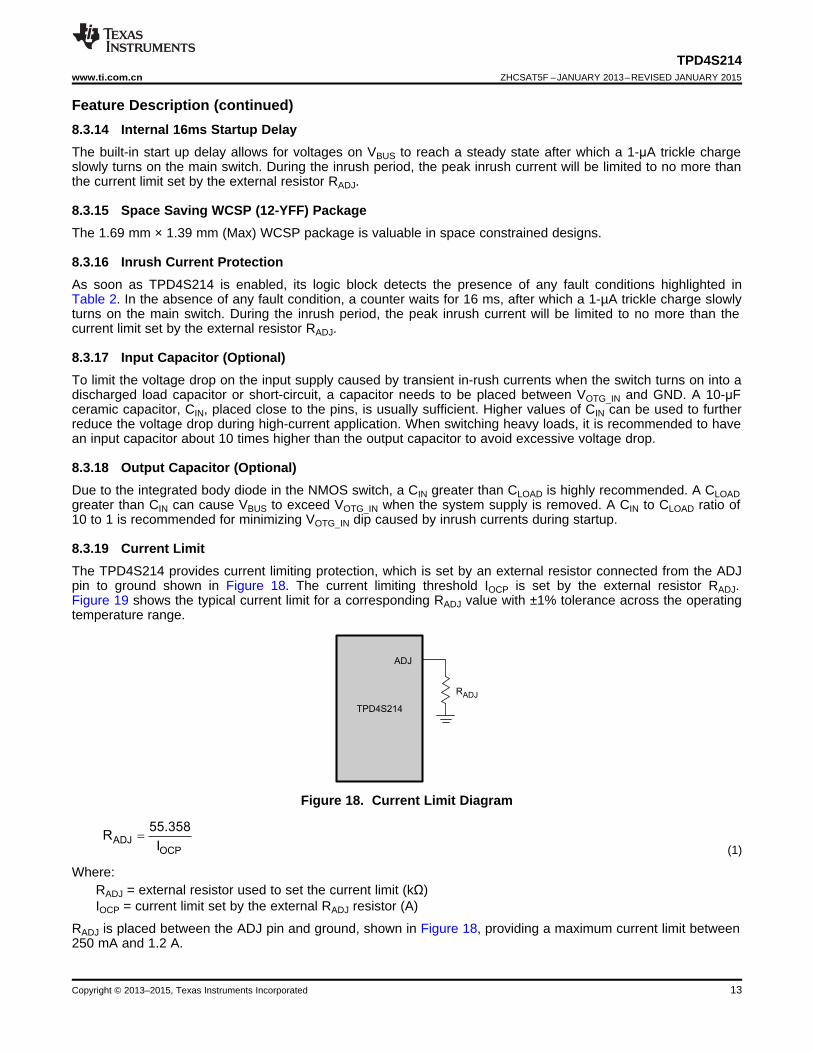
8.3.19 Current LimitThe TPD4S214 provides current limiting protection, which is set by an external resistor connected from the ADJpin to ground shown in Figure 18. The current limiting threshold IOCP is set by the external resistor RADJ.Figure 19 shows the typical current limit for a corresponding RADJ value with ±1% tolerance across the operatingtemperature range.
Figure 18. Current Limit Diagram
(1)
Where:RADJ = external resistor used to set the current limit (kΩ)IOCP = current limit set by the external RADJ resistor (A)
RADJ is placed between the ADJ pin and ground, shown in Figure 18, providing a maximum current limit between250 mA and 1.2 A.
Copyright © 2013–2015, Texas Instruments Incorporated 13
Current (A)
Junc
tion
Tem
pera
ture
(°C
)
0 0.2 0.4 0.6 0.8 1 1.2 1.425
45
65
85
105
125
1455 yrs. at 100% Duty Cycle
0.0
0.2
0.4
0.6
0.8
1.0
1.2
1.4
1.6
1.8
0 50 100 150 200 250 300 350 400
Cur
rent
(A
)
RADJ (k )
±40C
25C
85C
C001
TPD4S214ZHCSAT5F –JANUARY 2013–REVISED JANUARY 2015 www.ti.com.cn
Feature Description (continued)
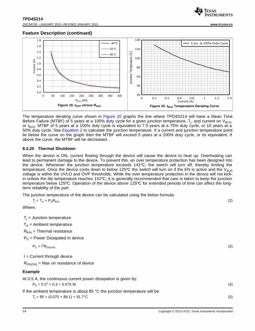
Figure 19. IOCP versus RADJ Figure 20. IBUS Temperature Derating Curve
The temperature derating curve shown in Figure 20 graphs the line where TPD4S214 will have a Mean TimeBefore Failure (MTBF) of 5 years at a 100% duty cycle for a given junction temperature, Tj, and current on VBUS,or IBUS. MTBF of 5 years at a 100% duty cycle is equivalent to 7.5 years at a 75% duty cycle, or 10 years at a50% duty cycle. See Equation 2 to calculate the junction temperature. If a current and junction temperature pointlie below the curve on the graph then the MTBF will exceed 5 years at a 100% duty cycle, or its equivalent. Ifabove the curve, the MTBF will be decreased.
8.3.20 Thermal ShutdownWhen the device is ON, current flowing through the device will cause the device to heat up. Overheating canlead to permanent damage to the device. To prevent this, an over temperature protection has been designed intothe device. Whenever the junction temperature exceeds 141ºC, the switch will turn off, thereby limiting thetemperature. Once the device cools down to below 125ºC the switch will turn on if the EN is active and the VBUSvoltage is within the UVLO and OVP thresholds. While the over temperature protection in the device will not kick-in unless the die temperature reaches 141ºC, it is generally recommended that care is taken to keep the junctiontemperature below 125ºC. Operation of the device above 125ºC for extended periods of time can affect the long-term reliability of the part.
The junction temperature of the device can be calculated using the below formula:Tj = TA + PDRθJA (2)
Where:
Tj = Junction temperatureTA = Ambient temperatureRθJA = Thermal resistancePD = Power Dissipated in device
PD = I2RDS(ON) (3)
I = Current through deviceRDS(ON) = Max on resistance of device
ExampleAt 0.5 A, the continuous current power dissipation is given by:
PD = 0.52 × 0.3 = 0.075 W (4)
If the ambient temperature is about 85 °C the junction temperature will be:Tj = 85 + (0.075 × 89.1) = 91.7°C (5)
14 Copyright © 2013–2015, Texas Instruments Incorporated
TPD4S214www.ti.com.cn ZHCSAT5F –JANUARY 2013–REVISED JANUARY 2015
Feature Description (continued)This implies that, at an ambient temperature of 85ºC, TPD4S214 can pass a continuous 0.5 A without sustainingdamage. Conversely, the above calculation can also be used to calculate the total continuous current theTPD4S214 can handle at any given temperature.
The MTBF can be estimated by examining Figure 20. Locating 0.5 A and 91.7 °C, the point is below the curve.This implies that the MTBF for this calculation is longer than 5 years at a 100% duty cycle. If the duty cycle is50% then MTBF exceeds 10 years.
8.3.21 VBUS DetectionThere are several important protocols defined in [OTG and EH Supplement] that governs communicationbetween Targeted Hosts (A-device) and USB peripherals (B-device). Communication between host andperipheral is usually done on the ID pin only. In the case when two OTG devices that could both act as eitherhost or peripheral are connected, measuring voltage level on VBUS will aid in the handshaking process. If anembedded host instead of a USB peripheral is connected to the OTG device, OTG charging would not berequired and the system’s OTG source should remain off to conserve power. The TPD4S214 VBUS detectionblock aids power conservation and is powered from VBUS. See Functional Block Diagram. The DET pin is anopen drain PMOS output with default state low.
In the event when an A-plug is attached, the system detects ID pin as FALSE, in which case ID pin resistance toground is less than 10 Ω. For a B-plug, the system detects ID pin as TRUE and ID pin resistance to ground isgreater than 100 kΩ. For the system to power a USB device through OTG switch once it is connected, voltage onVBUS should remain below VBUS_VALID MIN within TA_VBUS_ATT of the ID pin becoming FALSE. After this event, thesystem confirms that the USB device requires power and enables both TPD4S214 and OTG source. However, ifVBUS_VALID is detected on VBUS within TA_VBUS_ATT of the ID pin becoming FALSE, there is either a system error orthe device connected does not require charging. OTG source remains switched off and the entire sequencewould restart when the system detects another FALSE on the ID pin.
Table 1. VBUS Detection schemeEN VOTG_IN (VBUS Detect Power) VBUS DET Condition
X X VBUS_VALID– < VBUS < VBUS_VALID+ H VBUS within VBUS_VALID
X X VBUS_VALID– > VBUS or VBUS > VBUS_VALID+ L VBUS outside of VBUS_VALID
X = Don’t Care, H = Signal High, and L = Signal Low
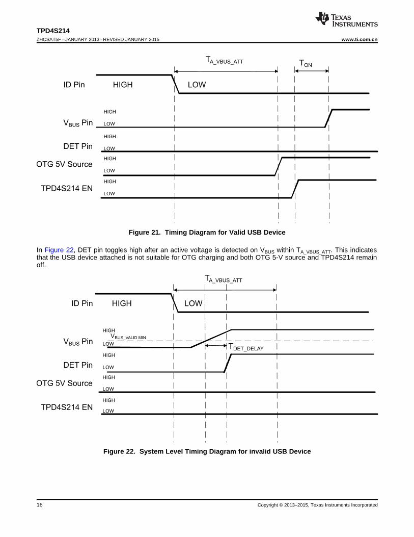
Figure 21 and Figure 22 shows suggested system level timing diagrams for detecting VBUS according to [OTGand EH Supplement]. Figure 28 shows the application diagram. In Figure 21, DET pin remains low after ID pinbecomes FALSE, indicating there is not an active voltage source on VBUS. The USB controller proceeds to turnon OTG 5-V source and the TPD4S214 respectively; this sequence is recommended because TPD4S214 ispowered through the OTG source. After a period of tON, current starts to flow through the OTG switch and VBUS isramped to the voltage level of VOTG_IN.
Copyright © 2013–2015, Texas Instruments Incorporated 15
ID Pin
OTG 5V Source
DET Pin
VBUS Pin
TA_VBUS_ATT
TDET_DELAY
VBUS_VALID MIN
TPD4S214 EN
HIGH
LOW
HIGH
LOW
HIGH
LOW
HIGH
LOW
HIGH LOW
ID Pin
OTG 5V Source
DET Pin
VBUS Pin
TA_VBUS_ATT
TPD4S214 EN
HIGH
LOW
HIGH
LOW
HIGH
LOW
HIGH
LOW
HIGH LOW
TON
TPD4S214ZHCSAT5F –JANUARY 2013–REVISED JANUARY 2015 www.ti.com.cn
Figure 21. Timing Diagram for Valid USB Device
In Figure 22, DET pin toggles high after an active voltage is detected on VBUS within TA_VBUS_ATT. This indicatesthat the USB device attached is not suitable for OTG charging and both OTG 5-V source and TPD4S214 remainoff.
Figure 22. System Level Timing Diagram for invalid USB Device
16 Copyright © 2013–2015, Texas Instruments Incorporated
CIN
ADJ
VOTG_IN VBUS
EN
TPD4S214
CLOAD
75 kΩ
RLOAD
TPD4S214www.ti.com.cn ZHCSAT5F –JANUARY 2013–REVISED JANUARY 2015
8.3.22 Test Configuration
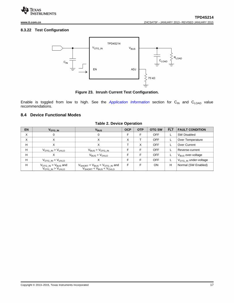
Figure 23. Inrush Current Test Configuration.
Enable is toggled from low to high. See the Application Information section for CIN and CLOAD valuerecommendations.
8.4 Device Functional Modes
Table 2. Device OperationEN VOTG_IN VBUS OCP OTP OTG SW FLT FAULT CONDITIONX 0 0 F F OFF L SW DisabledX X X X T OFF L Over TemperatureH X X T X OFF L Over CurrentH VOTG_IN > VUVLO VBUS > VOTG_IN F F OFF L Reverse-currentH X VBUS > VOVLO F F OFF L VBUS over-voltageH VOTG_IN < VUVLO X F F OFF L VOTG_IN under-voltageH VOTG_IN > VBUS and VSHORT < VBUS < VOTG_IN and F F ON H Normal (SW Enabled)
VOTG_IN > VUVLO VSHORT < VBUS < VOVLO
Copyright © 2013–2015, Texas Instruments Incorporated 17
OTG 5 VSource
COTG*
USB Controller+
Detection
System Side Supply(1.8 V to 3.6 V)
ADJ
VOTG_IN
VBUS
D+
D–
ID
DET
FLT EN
GND
CBUS*
VBUS
D+
D–
ID
TPD4S214
USB Connector
TPD4S214ZHCSAT5F –JANUARY 2013–REVISED JANUARY 2015 www.ti.com.cn
9 Application and Implementation
NOTEInformation in the following applications sections is not part of the TI componentspecification, and TI does not warrant its accuracy or completeness. TI’s customers areresponsible for determining suitability of components for their purposes. Customers shouldvalidate and test their design implementation to confirm system functionality.
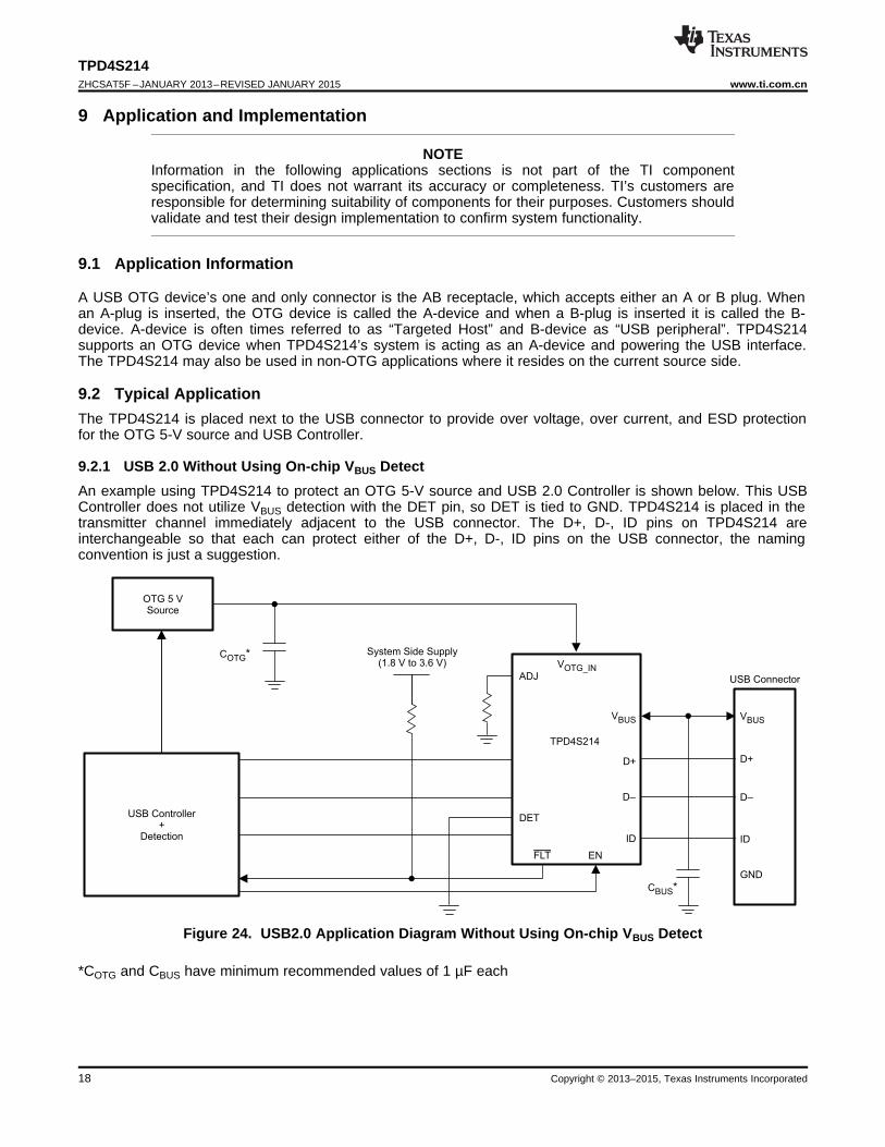
9.1 Application Information
A USB OTG device’s one and only connector is the AB receptacle, which accepts either an A or B plug. Whenan A-plug is inserted, the OTG device is called the A-device and when a B-plug is inserted it is called the B-device. A-device is often times referred to as “Targeted Host” and B-device as “USB peripheral”. TPD4S214supports an OTG device when TPD4S214’s system is acting as an A-device and powering the USB interface.The TPD4S214 may also be used in non-OTG applications where it resides on the current source side.
9.2 Typical ApplicationThe TPD4S214 is placed next to the USB connector to provide over voltage, over current, and ESD protectionfor the OTG 5-V source and USB Controller.
9.2.1 USB 2.0 Without Using On-chip VBUS DetectAn example using TPD4S214 to protect an OTG 5-V source and USB 2.0 Controller is shown below. This USBController does not utilize VBUS detection with the DET pin, so DET is tied to GND. TPD4S214 is placed in thetransmitter channel immediately adjacent to the USB connector. The D+, D-, ID pins on TPD4S214 areinterchangeable so that each can protect either of the D+, D-, ID pins on the USB connector, the namingconvention is just a suggestion.
Figure 24. USB2.0 Application Diagram Without Using On-chip VBUS Detect
*COTG and CBUS have minimum recommended values of 1 µF each
18 Copyright © 2013–2015, Texas Instruments Incorporated
TPD4S214www.ti.com.cn ZHCSAT5F –JANUARY 2013–REVISED JANUARY 2015
Typical Application (continued)9.2.1.1 Design RequirementsFor this example, use the following table as input parameters:
Design Parameters Example ValueSignal range on VOTG_IN 3.8 V – 5.5 VSignal range on VBUS 0 V – 5.3 V nominal, withstand -7 V to 30 VIBUS_MAX 500 mARADJ 100 kΩDrive EN low (disabled) 0 V – 0.4 VDrive EN high (enabled) 1.2 V – 5.5 V
9.2.1.2 Detailed Design ProcedureTo begin the design process, determine the maximum current expected under normal usage. In this example, themaximum expected current is 500 mA so an RADJ of 100 kΩ was selected to begin current limiting at around 550mA and protect the OTG system. Fault conditions are monitored by the USB controller by using the FLT Pin.DET is not used and is grounded and can optionally be left floating instead.
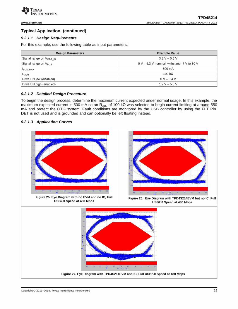
9.2.1.3 Application Curves
Figure 25. Eye Diagram with no EVM and no IC, Full Figure 26. Eye Diagram with TPD4S214EVM but no IC, FullUSB2.0 Speed at 480 Mbps USB2.0 Speed at 480 Mbps
Figure 27. Eye Diagram with TPD4S214EVM and IC, Full USB2.0 Speed at 480 Mbps
Copyright © 2013–2015, Texas Instruments Incorporated 19
OTG 5 VSource
COTG*
USB Controller
ADJ
VOTG_IN
VBUS
D+
D–
ID
DET
FLT EN
GND
CBUS*
VBUS
D+
D–
ID
TPD4S214
USB Connector
System Side Supply(1.8 V to 3.6 V)
TPD4S214ZHCSAT5F –JANUARY 2013–REVISED JANUARY 2015 www.ti.com.cn
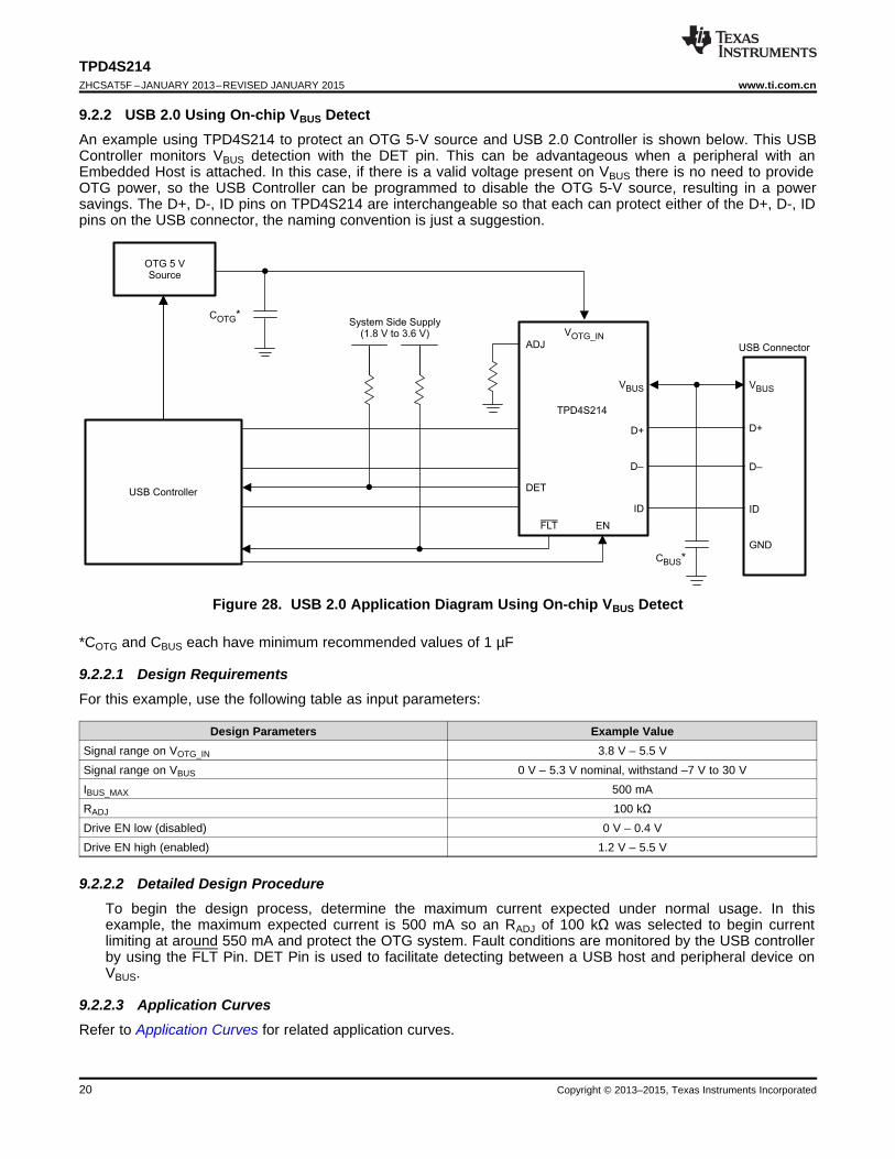
9.2.2 USB 2.0 Using On-chip VBUS DetectAn example using TPD4S214 to protect an OTG 5-V source and USB 2.0 Controller is shown below. This USBController monitors VBUS detection with the DET pin. This can be advantageous when a peripheral with anEmbedded Host is attached. In this case, if there is a valid voltage present on VBUS there is no need to provideOTG power, so the USB Controller can be programmed to disable the OTG 5-V source, resulting in a powersavings. The D+, D-, ID pins on TPD4S214 are interchangeable so that each can protect either of the D+, D-, IDpins on the USB connector, the naming convention is just a suggestion.
Figure 28. USB 2.0 Application Diagram Using On-chip VBUS Detect
*COTG and CBUS each have minimum recommended values of 1 µF
9.2.2.1 Design RequirementsFor this example, use the following table as input parameters:
Design Parameters Example ValueSignal range on VOTG_IN 3.8 V – 5.5 VSignal range on VBUS 0 V – 5.3 V nominal, withstand –7 V to 30 VIBUS_MAX 500 mARADJ 100 kΩDrive EN low (disabled) 0 V – 0.4 VDrive EN high (enabled) 1.2 V – 5.5 V
9.2.2.2 Detailed Design ProcedureTo begin the design process, determine the maximum current expected under normal usage. In thisexample, the maximum expected current is 500 mA so an RADJ of 100 kΩ was selected to begin currentlimiting at around 550 mA and protect the OTG system. Fault conditions are monitored by the USB controllerby using the FLT Pin. DET Pin is used to facilitate detecting between a USB host and peripheral device onVBUS.
9.2.2.3 Application CurvesRefer to Application Curves for related application curves.
20 Copyright © 2013–2015, Texas Instruments Incorporated
OTG 5 VSource
COTG*
USB Controller+
Detection
System Side Supply(1.8 V to 3.6 V)
ADJ
VOTG_IN
VBUS
D+
D–
ID
DET
FLT EN
GND
CBUS*
VBUS
D+
D–
TPD4S214
USB Connector
TX+
TX–
GND
RX+
RX–
TPD4S214www.ti.com.cn ZHCSAT5F –JANUARY 2013–REVISED JANUARY 2015
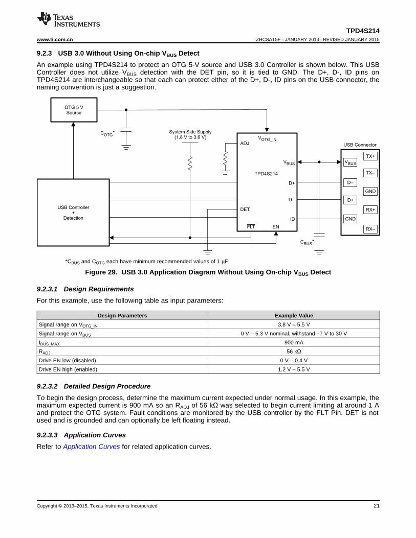
9.2.3 USB 3.0 Without Using On-chip VBUS DetectAn example using TPD4S214 to protect an OTG 5-V source and USB 3.0 Controller is shown below. This USBController does not utilize VBUS detection with the DET pin, so it is tied to GND. The D+, D-, ID pins onTPD4S214 are interchangeable so that each can protect either of the D+, D-, ID pins on the USB connector, thenaming convention is just a suggestion.
*CBUS and COTG each have minimum recommended values of 1 µF
Figure 29. USB 3.0 Application Diagram Without Using On-chip VBUS Detect
9.2.3.1 Design RequirementsFor this example, use the following table as input parameters:
Design Parameters Example ValueSignal range on VOTG_IN 3.8 V – 5.5 VSignal range on VBUS 0 V – 5.3 V nominal, withstand –7 V to 30 VIBUS_MAX 900 mARADJ 56 kΩDrive EN low (disabled) 0 V – 0.4 VDrive EN high (enabled) 1.2 V – 5.5 V
9.2.3.2 Detailed Design ProcedureTo begin the design process, determine the maximum current expected under normal usage. In this example, themaximum expected current is 900 mA so an RADJ of 56 kΩ was selected to begin current limiting at around 1 Aand protect the OTG system. Fault conditions are monitored by the USB controller by the FLT Pin. DET is notused and is grounded and can optionally be left floating instead.
9.2.3.3 Application CurvesRefer to Application Curves for related application curves.
Copyright © 2013–2015, Texas Instruments Incorporated 21
USB Connector
VIA to GND Plane
Top Layer
Pin to GND
Legend
Bottom Layer
VIA in SMD
A1
DET
FLT
VOTG_IN
EN
IDVBUS
D-D+
ID
D+D–
GND Plane Detail
0.1 mm (4 mil) clearance
VIA to copper
Copper pour
GND VIA:0.254 mm (10 mil) pad,
0.152 mm (6 mil) drill.Epoxy filled and plated.
TPD4S214ZHCSAT5F –JANUARY 2013–REVISED JANUARY 2015 www.ti.com.cn
10 Power Supply RecommendationsTPD4S214 Is designed to receive power from an OTG 5-V power source. It can operate normally (nFET ON)between 3.8 V and 5.55 V. Thus, the power supply (with a ripple of VRIPPLE) requirement for TPD4S214 to beable to switch the nFET ON is between 3.8 V + VRIPPLE and 5.55 V – VRIPPLE.
11 Layout
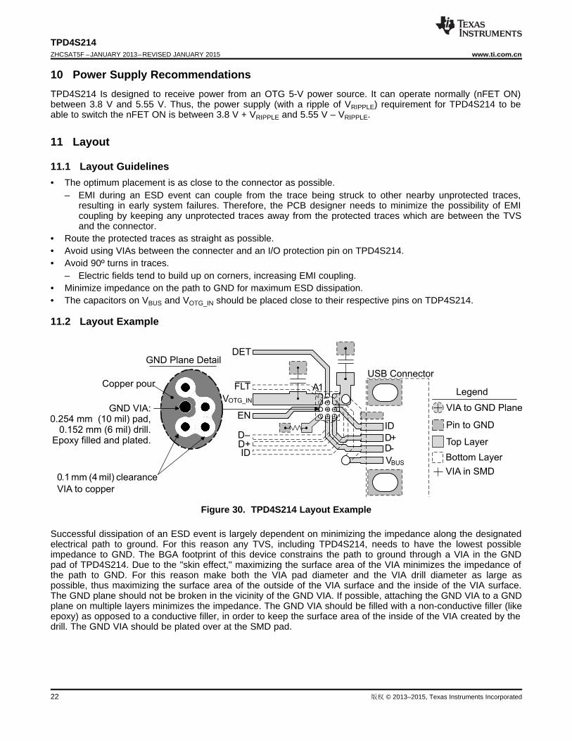
11.1 Layout Guidelines• The optimum placement is as close to the connector as possible.
– EMI during an ESD event can couple from the trace being struck to other nearby unprotected traces,resulting in early system failures. Therefore, the PCB designer needs to minimize the possibility of EMIcoupling by keeping any unprotected traces away from the protected traces which are between the TVSand the connector.
• Route the protected traces as straight as possible.• Avoid using VIAs between the connecter and an I/O protection pin on TPD4S214.• Avoid 90º turns in traces.
– Electric fields tend to build up on corners, increasing EMI coupling.• Minimize impedance on the path to GND for maximum ESD dissipation.• The capacitors on VBUS and VOTG_IN should be placed close to their respective pins on TDP4S214.
11.2 Layout Example
Figure 30. TPD4S214 Layout Example
Successful dissipation of an ESD event is largely dependent on minimizing the impedance along the designatedelectrical path to ground. For this reason any TVS, including TPD4S214, needs to have the lowest possibleimpedance to GND. The BGA footprint of this device constrains the path to ground through a VIA in the GNDpad of TPD4S214. Due to the "skin effect," maximizing the surface area of the VIA minimizes the impedance ofthe path to GND. For this reason make both the VIA pad diameter and the VIA drill diameter as large aspossible, thus maximizing the surface area of the outside of the VIA surface and the inside of the VIA surface.The GND plane should not be broken in the vicinity of the GND VIA. If possible, attaching the GND VIA to a GNDplane on multiple layers minimizes the impedance. The GND VIA should be filled with a non-conductive filler (likeepoxy) as opposed to a conductive filler, in order to keep the surface area of the inside of the VIA created by thedrill. The GND VIA should be plated over at the SMD pad.
22 版权 © 2013–2015, Texas Instruments Incorporated
TPD4S214www.ti.com.cn ZHCSAT5F –JANUARY 2013–REVISED JANUARY 2015
12 器器件件和和文文档档支支持持
12.1 文文档档支支持持
12.1.1 相相关关文文档档
OTG 和 EH 补充协议:USB 版本 2.0 规范的 On-The-Go 和嵌入式主机补充协议,2011 年 7 月 14日。www.usb.org
12.2 商商标标
All trademarks are the property of their respective owners.
12.3 静静电电放放电电警警告告
这些装置包含有限的内置 ESD 保护。 存储或装卸时,应将导线一起截短或将装置放置于导电泡棉中,以防止 MOS 门极遭受静电损伤。
12.4 术术语语表表
SLYZ022 — TI 术语表。
这份术语表列出并解释术语、首字母缩略词和定义。
13 机机械械封封装装和和可可订订购购信信息息
以下页中包括机械封装和可订购信息。 这些信息是针对指定器件可提供的最新数据。 这些数据会在无通知且不对本文档进行修订的情况下发生改变。 欲获得该数据表的浏览器版本,请查阅左侧的导航栏。
版权 © 2013–2015, Texas Instruments Incorporated 23
重重要要声声明明
德州仪器(TI) 及其下属子公司有权根据 JESD46 最新标准, 对所提供的产品和服务进行更正、修改、增强、改进或其它更改, 并有权根据JESD48 最新标准中止提供任何产品和服务。客户在下订单前应获取最新的相关信息, 并验证这些信息是否完整且是最新的。所有产品的销售都遵循在订单确认时所提供的TI 销售条款与条件。
TI 保证其所销售的组件的性能符合产品销售时 TI 半导体产品销售条件与条款的适用规范。仅在 TI 保证的范围内,且 TI 认为 有必要时才会使用测试或其它质量控制技术。除非适用法律做出了硬性规定,否则没有必要对每种组件的所有参数进行测试。
TI 对应用帮助或客户产品设计不承担任何义务。客户应对其使用 TI 组件的产品和应用自行负责。为尽量减小与客户产品和应 用相关的风险,客户应提供充分的设计与操作安全措施。
TI 不对任何 TI 专利权、版权、屏蔽作品权或其它与使用了 TI 组件或服务的组合设备、机器或流程相关的 TI 知识产权中授予 的直接或隐含权限作出任何保证或解释。TI 所发布的与第三方产品或服务有关的信息,不能构成从 TI 获得使用这些产品或服 务的许可、授权、或认可。使用此类信息可能需要获得第三方的专利权或其它知识产权方面的许可,或是 TI 的专利权或其它 知识产权方面的许可。
对于 TI 的产品手册或数据表中 TI 信息的重要部分,仅在没有对内容进行任何篡改且带有相关授权、条件、限制和声明的情况 下才允许进行复制。TI 对此类篡改过的文件不承担任何责任或义务。复制第三方的信息可能需要服从额外的限制条件。
在转售 TI 组件或服务时,如果对该组件或服务参数的陈述与 TI 标明的参数相比存在差异或虚假成分,则会失去相关 TI 组件 或服务的所有明示或暗示授权,且这是不正当的、欺诈性商业行为。TI 对任何此类虚假陈述均不承担任何责任或义务。
客户认可并同意,尽管任何应用相关信息或支持仍可能由 TI 提供,但他们将独力负责满足与其产品及在其应用中使用 TI 产品 相关的所有法律、法规和安全相关要求。客户声明并同意,他们具备制定与实施安全措施所需的全部专业技术和知识,可预见 故障的危险后果、监测故障及其后果、降低有可能造成人身伤害的故障的发生机率并采取适当的补救措施。客户将全额赔偿因 在此类安全关键应用中使用任何 TI 组件而对 TI 及其代理造成的任何损失。
在某些场合中,为了推进安全相关应用有可能对 TI 组件进行特别的促销。TI 的目标是利用此类组件帮助客户设计和创立其特 有的可满足适用的功能安全性标准和要求的终端产品解决方案。尽管如此,此类组件仍然服从这些条款。
TI 组件未获得用于 FDA Class III(或类似的生命攸关医疗设备)的授权许可,除非各方授权官员已经达成了专门管控此类使 用的特别协议。
只有那些 TI 特别注明属于军用等级或“增强型塑料”的 TI 组件才是设计或专门用于军事/航空应用或环境的。购买者认可并同 意,对并非指定面向军事或航空航天用途的 TI 组件进行军事或航空航天方面的应用,其风险由客户单独承担,并且由客户独 力负责满足与此类使用相关的所有法律和法规要求。
TI 已明确指定符合 ISO/TS16949 要求的产品,这些产品主要用于汽车。在任何情况下,因使用非指定产品而无法达到 ISO/TS16949 要求,TI不承担任何责任。
产品 应用
数字音频 www.ti.com.cn/audio 通信与电信 www.ti.com.cn/telecom放大器和线性器件 www.ti.com.cn/amplifiers 计算机及周边 www.ti.com.cn/computer数据转换器 www.ti.com.cn/dataconverters 消费电子 www.ti.com/consumer-appsDLP® 产品 www.dlp.com 能源 www.ti.com/energyDSP - 数字信号处理器 www.ti.com.cn/dsp 工业应用 www.ti.com.cn/industrial时钟和计时器 www.ti.com.cn/clockandtimers 医疗电子 www.ti.com.cn/medical接口 www.ti.com.cn/interface 安防应用 www.ti.com.cn/security逻辑 www.ti.com.cn/logic 汽车电子 www.ti.com.cn/automotive电源管理 www.ti.com.cn/power 视频和影像 www.ti.com.cn/video微控制器 (MCU) www.ti.com.cn/microcontrollersRFID 系统 www.ti.com.cn/rfidsysOMAP应用处理器 www.ti.com/omap无线连通性 www.ti.com.cn/wirelessconnectivity 德州仪器在线技术支持社区 www.deyisupport.com
IMPORTANT NOTICE
邮寄地址: 上海市浦东新区世纪大道1568 号,中建大厦32 楼邮政编码: 200122Copyright © 2015, 德州仪器半导体技术(上海)有限公司
PACKAGE OPTION ADDENDUM
www.ti.com 10-Dec-2020
Addendum-Page 1
PACKAGING INFORMATION
Orderable Device Status(1)
Package Type PackageDrawing
Pins PackageQty
Eco Plan(2)
Lead finish/Ball material
(6)
MSL Peak Temp(3)
Op Temp (°C) Device Marking(4/5)
Samples
TPD4S214YFFR ACTIVE DSBGA YFF 12 3000 RoHS & Green SNAGCU Level-1-260C-UNLIM -40 to 85 B3214
(1) The marketing status values are defined as follows:ACTIVE: Product device recommended for new designs.LIFEBUY: TI has announced that the device will be discontinued, and a lifetime-buy period is in effect.NRND: Not recommended for new designs. Device is in production to support existing customers, but TI does not recommend using this part in a new design.PREVIEW: Device has been announced but is not in production. Samples may or may not be available.OBSOLETE: TI has discontinued the production of the device.
(2) RoHS: TI defines "RoHS" to mean semiconductor products that are compliant with the current EU RoHS requirements for all 10 RoHS substances, including the requirement that RoHS substancedo not exceed 0.1% by weight in homogeneous materials. Where designed to be soldered at high temperatures, "RoHS" products are suitable for use in specified lead-free processes. TI mayreference these types of products as "Pb-Free".RoHS Exempt: TI defines "RoHS Exempt" to mean products that contain lead but are compliant with EU RoHS pursuant to a specific EU RoHS exemption.Green: TI defines "Green" to mean the content of Chlorine (Cl) and Bromine (Br) based flame retardants meet JS709B low halogen requirements of <=1000ppm threshold. Antimony trioxide basedflame retardants must also meet the <=1000ppm threshold requirement.
(3) MSL, Peak Temp. - The Moisture Sensitivity Level rating according to the JEDEC industry standard classifications, and peak solder temperature.
(4) There may be additional marking, which relates to the logo, the lot trace code information, or the environmental category on the device.
(5) Multiple Device Markings will be inside parentheses. Only one Device Marking contained in parentheses and separated by a "~" will appear on a device. If a line is indented then it is a continuationof the previous line and the two combined represent the entire Device Marking for that device.
(6) Lead finish/Ball material - Orderable Devices may have multiple material finish options. Finish options are separated by a vertical ruled line. Lead finish/Ball material values may wrap to twolines if the finish value exceeds the maximum column width.
Important Information and Disclaimer:The information provided on this page represents TI's knowledge and belief as of the date that it is provided. TI bases its knowledge and belief on informationprovided by third parties, and makes no representation or warranty as to the accuracy of such information. Efforts are underway to better integrate information from third parties. TI has taken andcontinues to take reasonable steps to provide representative and accurate information but may not have conducted destructive testing or chemical analysis on incoming materials and chemicals.TI and TI suppliers consider certain information to be proprietary, and thus CAS numbers and other limited information may not be available for release.
In no event shall TI's liability arising out of such information exceed the total purchase price of the TI part(s) at issue in this document sold by TI to Customer on an annual basis.
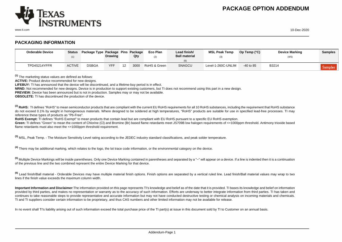
TAPE AND REEL INFORMATION
*All dimensions are nominal
Device PackageType
PackageDrawing
Pins SPQ ReelDiameter
(mm)
ReelWidth
W1 (mm)
A0(mm)
B0(mm)
K0(mm)
P1(mm)
W(mm)
Pin1Quadrant
TPD4S214YFFR DSBGA YFF 12 3000 180.0 8.4 1.48 1.78 0.69 4.0 8.0 Q1
PACKAGE MATERIALS INFORMATION
www.ti.com 17-Jun-2015
Pack Materials-Page 1
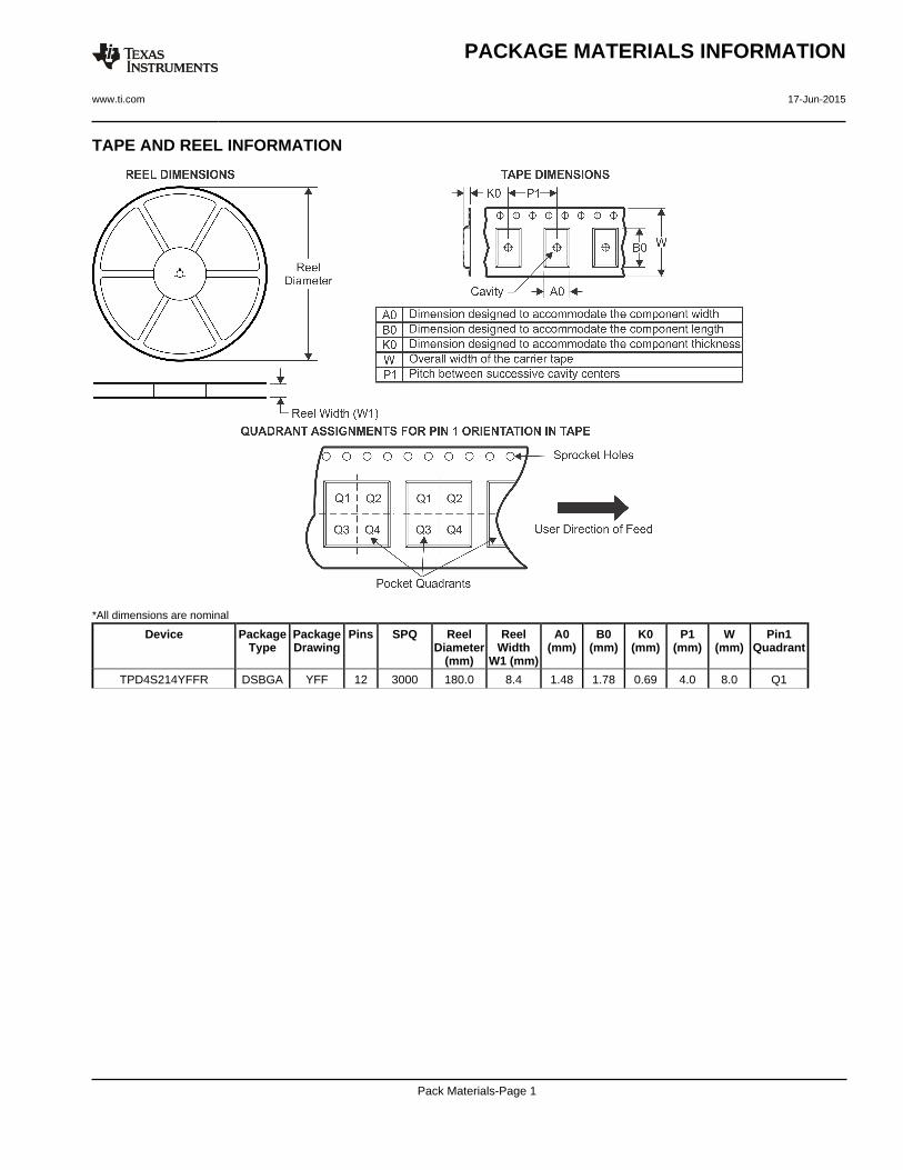
*All dimensions are nominal
Device Package Type Package Drawing Pins SPQ Length (mm) Width (mm) Height (mm)
TPD4S214YFFR DSBGA YFF 12 3000 182.0 182.0 20.0
PACKAGE MATERIALS INFORMATION
www.ti.com 17-Jun-2015
Pack Materials-Page 2
重重要要声声明明和和免免责责声声明明
TI 均以“原样”提供技术性及可靠性数据(包括数据表)、设计资源(包括参考设计)、应用或其他设计建议、网络工具、安全信息和其他资源,不保证其中不含任何瑕疵,且不做任何明示或暗示的担保,包括但不限于对适销性、适合某特定用途或不侵犯任何第三方知识产权的暗示担保。
所述资源可供专业开发人员应用TI 产品进行设计使用。您将对以下行为独自承担全部责任:(1) 针对您的应用选择合适的TI 产品;(2) 设计、验证并测试您的应用;(3) 确保您的应用满足相应标准以及任何其他安全、安保或其他要求。所述资源如有变更,恕不另行通知。TI 对您使用所述资源的授权仅限于开发资源所涉及TI 产品的相关应用。除此之外不得复制或展示所述资源,也不提供其它TI或任何第三方的知识产权授权许可。如因使用所述资源而产生任何索赔、赔偿、成本、损失及债务等,TI对此概不负责,并且您须赔偿由此对TI 及其代表造成的损害。
TI 所提供产品均受TI 的销售条款 (http://www.ti.com.cn/zh-cn/legal/termsofsale.html) 以及ti.com.cn上或随附TI产品提供的其他可适用条款的约束。TI提供所述资源并不扩展或以其他方式更改TI 针对TI 产品所发布的可适用的担保范围或担保免责声明。IMPORTANT NOTICE
邮寄地址:上海市浦东新区世纪大道 1568 号中建大厦 32 楼,邮政编码:200122Copyright © 2020 德州仪器半导体技术(上海)有限公司


