Embed Size (px)
Citation preview
www.ti.com
FEATURES APPLICATIONS
DESCRIPTION
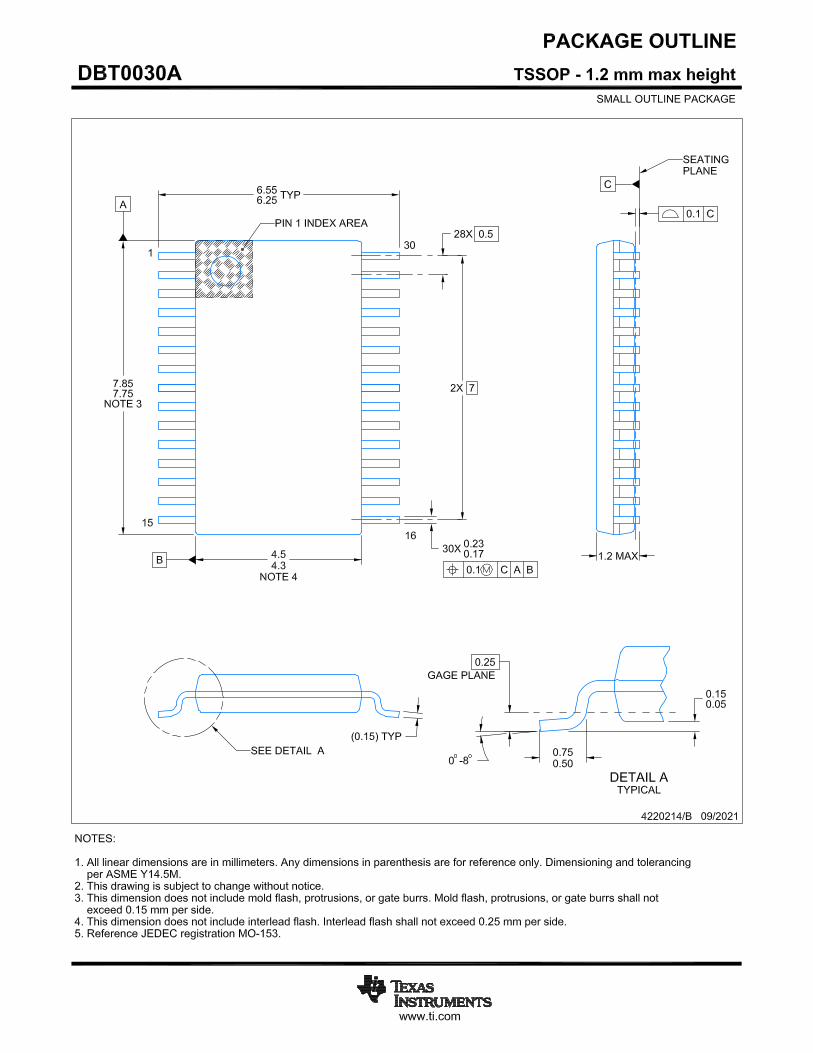
123
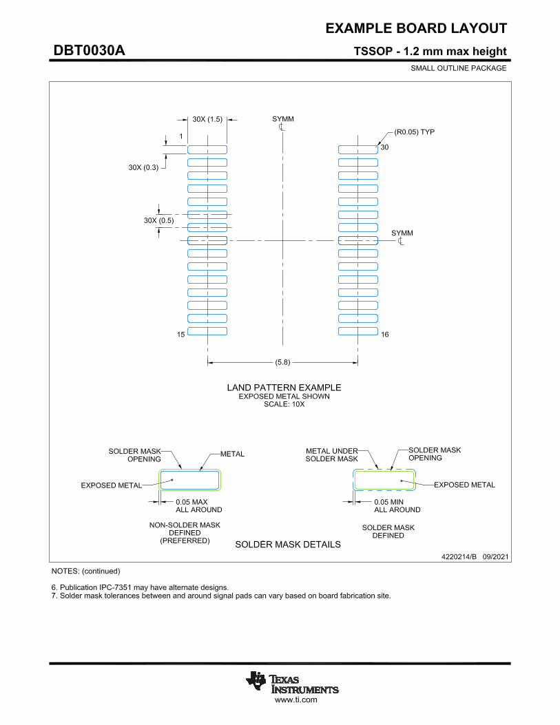
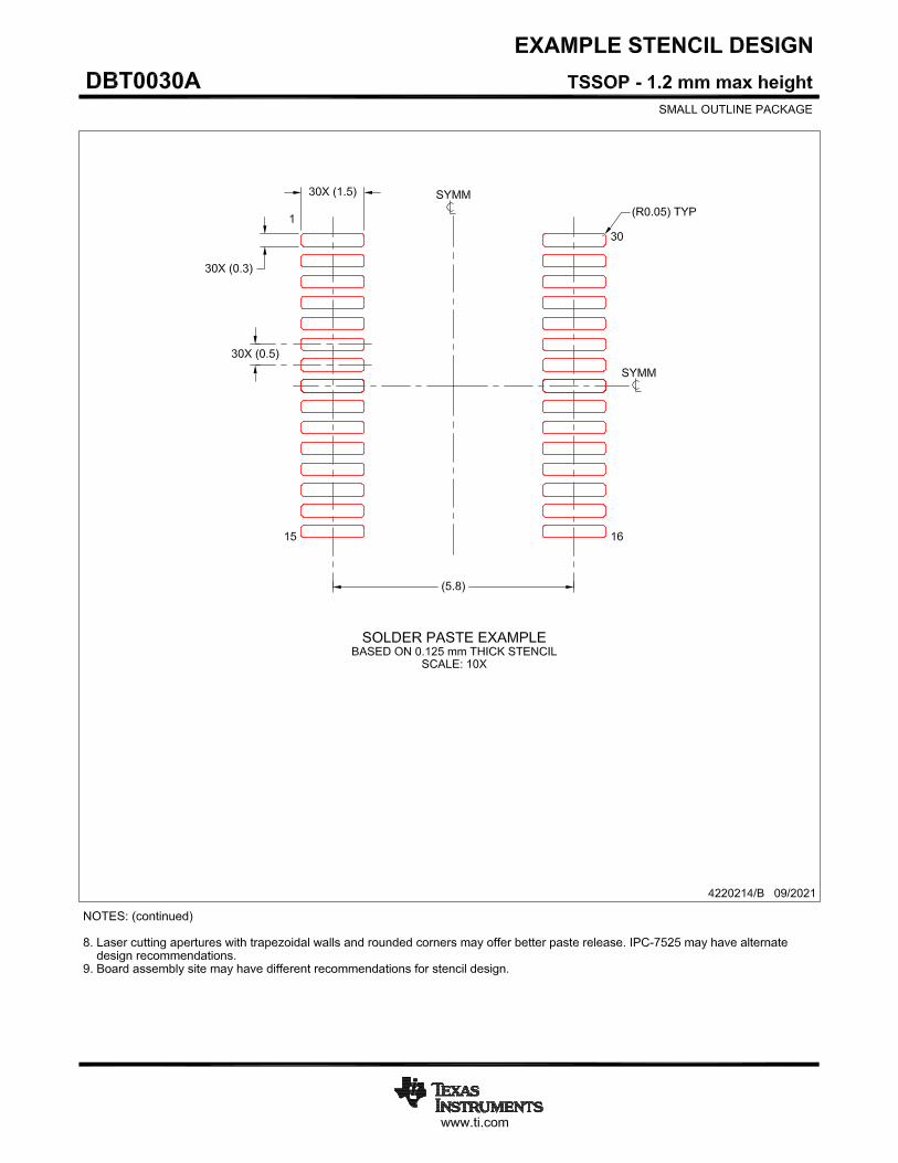
4 56789
101112131415
302928
272625242322
212019181716
LDRV1VIN5SW1
HDRV1BOOT1OVSET
VOUTGSNSDIFFO
CS1CSRT1COMPVREF
DROOPFB
PGNDLDRV2SW2HDRV2BOOT2SSUVLOBP5AGNDCS2CSRT2RTPGOODILIMEN/SYNC
DBT PACKAGE(TOP VIEW)
RHB PACKAGE(TOP VIEW)
32 31 30 29 28 27 26 2524
23
22
21
20
19
18
179 10 11 12 13 15 16
BOOT1
OVSET
VOUT
GSNS
DIFFO
CS1
CSRT1
NC
NC
BOOT2
SS
UVLO
BP5
AGND
CS2
CSRT2
CO
MP
HD
RV
1
SW
1
VIN
5LD
RV
1
PG
ND
LDR
V2
SW
2
HD
RV
2
VR
EF
DR
OO
P
FB
EN
/SY
NC
ILIM
PG
OO
D
RT
14
1
2
3
4
5
6
7
8
TPS40130SLUS602B–JUNE 2004–REVISED SEPTEMBER 2005
TWO-PHASE, SYNCHRONOUS BUCK CONTROLLER WITH INTEGRATED MOSFETDRIVERS
• Graphic Cards• Two-Phase Interleaved Operation• Internet Servers• 3-V to 40-V Power Stage Operation Range• Networking Equipment• Supports Up to 6-V VOUT With External Divider• Telecommunications Equipment• Requires VIN5 @ 50 mA, Typical, Depending• DC Power Distributed Systemson External MOSFETs and Switching
Frequency• 1-µA Shutdown Current
The TPS40130 is a two-phase synchronous buck• Programmable Switching Frequency up to 1controller that is optimized for low-output voltage,MHz/Phasehigh-output current applications powered from a
• Current Mode Control with Forced Current supply between 3 V and 40 V. A multi-phaseSharing converter offers several advantages over a single
power stage including lower current ripple on the• Better than 1% Internal 0.7-V Referenceinput and output capacitors, faster transient response• Resistive Divider Sets Direct Output Overto load steps, improved power handling capabilities,Voltage Threshold and Sets Inputand higher system efficiency.Undervoltage LockoutEach phase can be operated at a switching• True Remote Sensing Differential Amplifierfrequency up to 1 MHz, resulting in an effective• Resistive or Inductor’s DCR Current Sensing ripple frequency of up to 2 MHz at the input and the
• 30-pin TSSOP or 32-Pin QFN Packages output. The two phases operates 180 degreesout-of-phase.• Can Be Used with TPS40120 to Provide a 6-Bit
Digitally Controlled Output
Please be aware that an important notice concerning availability, standard warranty, and use in critical applications of TexasInstruments semiconductor products and disclaimers thereto appears at the end of this data sheet.
PRODUCTION DATA information is current as of publication date. Copyright © 2004–2005, Texas Instruments IncorporatedProducts conform to specifications per the terms of the TexasInstruments standard warranty. Production processing does notnecessarily include testing of all parameters.
www.ti.com
SIMPLIFIED APPLICATION DIAGRAM
1
2
3
4
30
29
28
27
PGND
LDRV2
SW2
HDRV2
LDRV1
VIN5
SW1
HDRV1
TPS40130DBT
5
6
7
8
BOOT1
OVSET
VOUT
GSNS
9
10
11
DIFFO
CS1
CSRT1
12
13
14
15
COMP
VREF
DROOP
FB
26
25
24
23
BOOT2
SS
UVLO
BP5
22
21
20
19
AGND
CS2
CSRT2
RT
18
17
16
PGOOD
ILIM
EN/SYNC
5 V
5 V
5 V
DIFFO
LOAD
UDG−04017
VOUTVIN
VIN
VIN
VREF
VOUT
TPS40130SLUS602B–JUNE 2004–REVISED SEPTEMBER 2005
These devices have limited built-in ESD protection. The leads should be shorted together or the device placed in conductive foamduring storage or handling to prevent electrostatic damage to the MOS gates.
2 Submit Documentation Feedback
www.ti.com
ABSOLUTE MAXIMUM RATING
RECOMMENDED OPERATING CONDITIONS
TPS40130SLUS602B–JUNE 2004–REVISED SEPTEMBER 2005
ORDERING INFORMATION
TA PACKAGE PART NUMBER
Plastic TSSOP(DBT) (1) TPS40130DBT (2) (3)
-40°C to 85°CPlastic QFN (RHB) TPS40130RHB
(1) The DBTpackage is also available taped and reeled. Add an R suffix to the device type (i.e.,TPS40130DBTR).
(2) The TPS40130DBTRG4 is a lead (Pb) free product, which means that it is compatible with currentRoHS requirements for all 6 substances, including the requirement that lead not exceed 0.1% byweight in homogeneous material. In addition, this part has NiPdAu plated copper lead frame and israted at MSL level 2 at 260°C according to JEDEC 020C Standards.
(3) Release date for the TPS40130DBTRG4 TBD.
over operating free-air temperature range unless otherwise noted (1)
TPS40130 UNITS
SW1, SW2 -1 to 44V
Input voltage range BOOT1, BOOT2 -0.3 to VSW + 6.0
All other pins -0.3 to 6.0
Sourcing current RT 200 µA
TJ Operating junction temperature range -40 to 125 °C
Tstg Storage temperature -55 to 150 °C
Lead temperature 1,6 mm (1/16 inch) from case for 10 seconds 260 °C
(1) Stresses beyond those listed under "absolute maximum ratings" may cause permanent damage to the device. These are stress ratingsonly, and functional operation of the device at these or any other conditions beyond those indicated under "recommended operatingconditions" is not implied. Exposure to absolute-maximum-rated conditions for extended periods may affect device reliability.
MIN NOM MAX UNIT
VIN Input voltage 3.0 40 V
TA Operating free-air temperature -40 85 °C
3Submit Documentation Feedback
www.ti.com
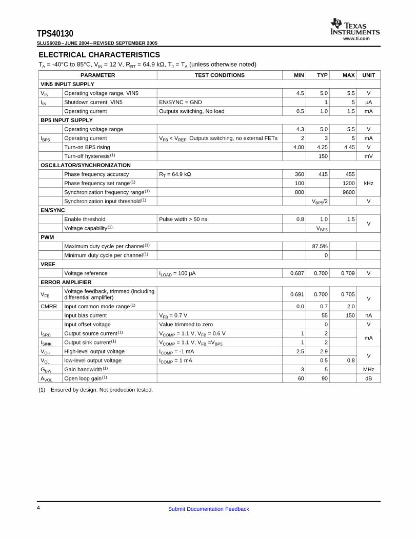
ELECTRICAL CHARACTERISTICS
TPS40130SLUS602B–JUNE 2004–REVISED SEPTEMBER 2005
TA = -40°C to 85°C, VIN = 12 V, RRT = 64.9 kΩ, TJ = TA (unless otherwise noted)
PARAMETER TEST CONDITIONS MIN TYP MAX UNIT
VIN5 INPUT SUPPLY
VIN Operating voltage range, VIN5 4.5 5.0 5.5 V
IIN Shutdown current, VIN5 EN/SYNC = GND 1 5 µA
Operating current Outputs switching, No load 0.5 1.0 1.5 mA
BP5 INPUT SUPPLY
Operating voltage range 4.3 5.0 5.5 V
IBP5 Operating current VFB < VREF, Outputs switching, no external FETs 2 3 5 mA
Turn-on BP5 rising 4.00 4.25 4.45 V
Turn-off hysteresis (1) 150 mV
OSCILLATOR/SYNCHRONIZATION
Phase frequency accuracy RT = 64.9 kΩ 360 415 455
Phase frequency set range (1) 100 1200 kHz
Synchronization frequency range (1) 800 9600
Synchronization input threshold (1) VBP5/2 V
EN/SYNC
Enable threshold Pulse width > 50 ns 0.8 1.0 1.5V
Voltage capability (1) VBP5
PWM
Maximum duty cycle per channel (1) 87.5%
Minimum duty cycle per channel (1) 0
VREF
Voltage reference ILOAD = 100 µA 0.687 0.700 0.709 V
ERROR AMPLIFIER
Voltage feedback, trimmed (includingVFB 0.691 0.700 0.705differential amplifier) VCMRR Input common mode range (1) 0.0 0.7 2.0
Input bias current VFB = 0.7 V 55 150 nA
Input offset voltage Value trimmed to zero 0 V
ISRC Output source current (1) VCOMP = 1.1 V, VFB = 0.6 V 1 2mA
ISINK Output sink current (1) VCOMP = 1.1 V, VFB =VBP5 1 2
VOH High-level output voltage ICOMP = -1 mA 2.5 2.9V
VOL low-level output voltage ICOMP = 1 mA 0.5 0.8
GBW Gain bandwidth (1) 3 5 MHz
AVOL Open loop gain (1) 60 90 dB
(1) Ensured by design. Not production tested.
4 Submit Documentation Feedback
www.ti.comTPS40130
SLUS602B–JUNE 2004–REVISED SEPTEMBER 2005
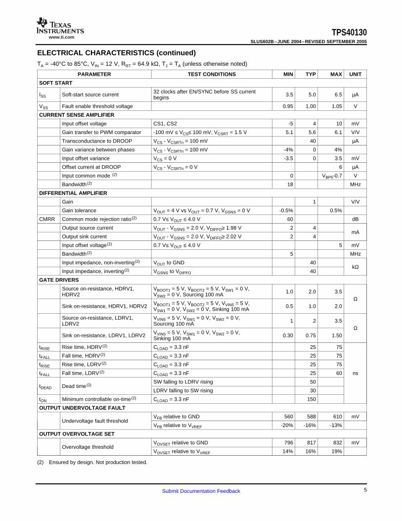
ELECTRICAL CHARACTERISTICS (continued)TA = -40°C to 85°C, VIN = 12 V, RRT = 64.9 kΩ, TJ = TA (unless otherwise noted)
PARAMETER TEST CONDITIONS MIN TYP MAX UNIT
SOFT START
32 clocks after EN/SYNC before SS currentISS Soft-start source current 3.5 5.0 6.5 µAbegins
VSS Fault enable threshold voltage 0.95 1.00 1.05 V
CURRENT SENSE AMPLIFIER
Input offset voltage CS1, CS2 -5 4 10 mV
Gain transfer to PWM comparator -100 mV ≤ VCS≤ 100 mV, VCSRT = 1.5 V 5.1 5.6 6.1 V/V
Transconductance to DROOP VCS - VCSRTn = 100 mV 40 µA
Gain variance between phases VCS - VCSRTn = 100 mV -4% 0 4%
Input offset variance VCS = 0 V -3.5 0 3.5 mV
Offset current at DROOP VCS - VCSRTn = 0 V 6 µA
Input common mode (2) 0 VBP5-0.7 V
Bandwidth (2) 18 MHz
DIFFERENTIAL AMPLIFIER
Gain 1 V/V
Gain tolerance VOUT = 4 V vs VOUT = 0.7 V, VGSNS = 0 V -0.5% 0.5%
CMRR Common mode rejection ratio (2) 0.7 V≤ VOUT ≤ 4.0 V 60 dB
Output source current VOUT - VGSNS = 2.0 V, VDIFFO≥ 1.98 V 2 4mA
Output sink current VOUT - VGSNS = 2.0 V, VDIFFO≥ 2.02 V 2 4
Input offset voltage (2) 0.7 V≤ VOUT ≤ 4.0 V 5 mV
Bandwidth (2) 5 MHz
Input impedance, non-inverting (2) VOUT to GND 40kΩ
Input impedance, inverting (2) VGSNS to VDIFFO 40
GATE DRIVERS
Source on-resistance, HDRV1, VBOOT1 = 5 V, VBOOT2 = 5 V, VSW1 = 0 V, 1.0 2.0 3.5HDRV2 VSW2 = 0 V, Sourcing 100 mAΩ
VBOOT1 = 5 V, VBOOT2 = 5 V, VVIN5 = 5 V,Sink on-resistance, HDRV1, HDRV2 0.5 1.0 2.0VSW1 = 0 V, VSW2 = 0 V, Sinking 100 mA
Source on-resistance, LDRV1, VVIN5 = 5 V, VSW1 = 0 V, VSW2 = 0 V, 1 2 3.5LDRV2 Sourcing 100 mAΩ
VVIN5 = 5 V, VSW1 = 0 V, VSW2 = 0 V,Sink on-resistance, LDRV1, LDRV2 0.30 0.75 1.50Sinking 100 mA
tRISE Rise time, HDRV (2) CLOAD = 3.3 nF 25 75
tFALL Fall time, HDRV (2) CLOAD = 3.3 nF 25 75
tRISE Rise time, LDRV (2) CLOAD = 3.3 nF 25 75
tFALL Fall time, LDRV (2) CLOAD = 3.3 nF 25 60 ns
SW falling to LDRV rising 50tDEAD Dead time (2)
LDRV falling to SW rising 30
tON Minimum controllable on-time (2) CLOAD = 3.3 nF 150
OUTPUT UNDERVOLTAGE FAULT
VFB relative to GND 560 588 610 mVUndervoltage fault threshold
VFB relative to VVREF -20% -16% -13%
OUTPUT OVERVOLTAGE SET
VOVSET relative to GND 796 817 832 mVOvervoltage threshold
VOVSET relative to VVREF 14% 16% 19%
(2) Ensured by design. Not production tested.
5Submit Documentation Feedback
www.ti.comTPS40130SLUS602B–JUNE 2004–REVISED SEPTEMBER 2005
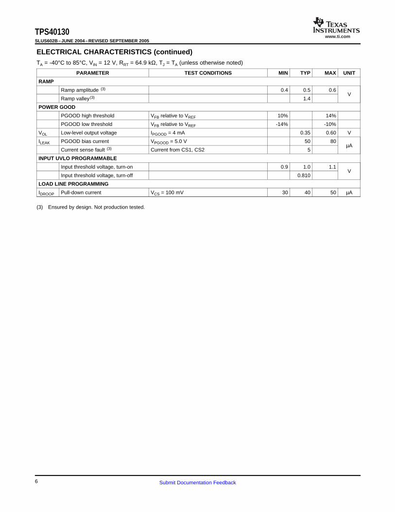
ELECTRICAL CHARACTERISTICS (continued)TA = -40°C to 85°C, VIN = 12 V, RRT = 64.9 kΩ, TJ = TA (unless otherwise noted)
PARAMETER TEST CONDITIONS MIN TYP MAX UNIT
RAMP
Ramp amplitude (3) 0.4 0.5 0.6V
Ramp valley (3) 1.4
POWER GOOD
PGOOD high threshold VFB relative to VREF 10% 14%
PGOOD low threshold VFB relative to VREF -14% -10%
VOL Low-level output voltage IPGOOD = 4 mA 0.35 0.60 V
ILEAK PGOOD bias current VPGOOD = 5.0 V 50 80µA
Current sense fault (3) Current from CS1, CS2 5
INPUT UVLO PROGRAMMABLE
Input threshold voltage, turn-on 0.9 1.0 1.1V
Input threshold voltage, turn-off 0.810
LOAD LINE PROGRAMMING
IDROOP Pull-down current VCS = 100 mV 30 40 50 µA
(3) Ensured by design. Not production tested.
6 Submit Documentation Feedback
www.ti.com
123
4 56789
101112131415
302928
272625242322
212019181716
LDRV1VIN5SW1
HDRV1BOOT1OVSET
VOUTGSNSDIFFO
CS1CSRT1COMPVREF
DROOPFB
PGNDLDRV2SW2HDRV2BOOT2SSUVLOBP5AGNDCS2CSRT2RTPGOODILIMEN/SYNC
DBT PACKAGE(TOP VIEW)
RHB PACKAGE(TOP VIEW)
32 31 30 29 28 27 26 2524
23
22
21
20
19
18
179 10 11 12 13 15 16
BOOT1
OVSET
VOUT
GSNS
DIFFO
CS1
CSRT1
NC
NC
BOOT2
SS
UVLO
BP5
AGND
CS2
CSRT2
CO
MP
HD
RV
1
SW
1
VIN
5LD
RV
1
PG
ND
LDR
V2
SW
2
HD
RV
2
VR
EF
DR
OO
P
FB
EN
/SY
NC
ILIM
PG
OO
D
RT
14
1
2
3
4
5
6
7
8
TPS40130SLUS602B–JUNE 2004–REVISED SEPTEMBER 2005
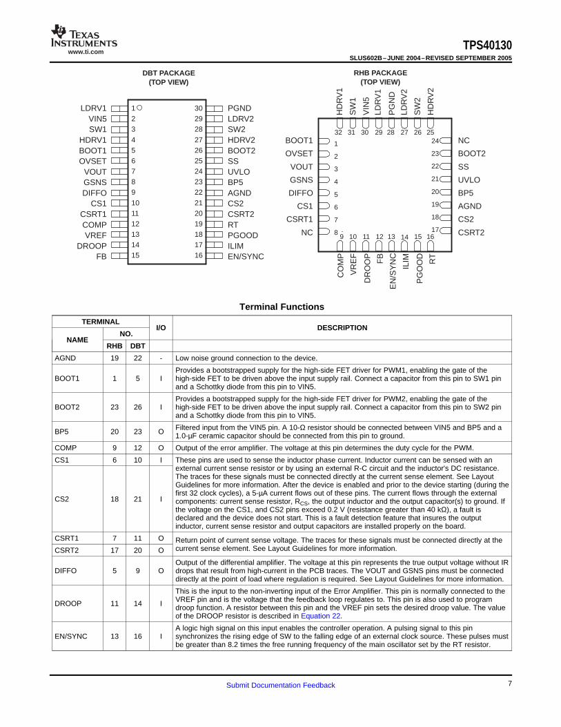
Terminal Functions
TERMINALI/O DESCRIPTION
NO.NAME
RHB DBT
AGND 19 22 - Low noise ground connection to the device.
Provides a bootstrapped supply for the high-side FET driver for PWM1, enabling the gate of theBOOT1 1 5 I high-side FET to be driven above the input supply rail. Connect a capacitor from this pin to SW1 pin
and a Schottky diode from this pin to VIN5.
Provides a bootstrapped supply for the high-side FET driver for PWM2, enabling the gate of theBOOT2 23 26 I high-side FET to be driven above the input supply rail. Connect a capacitor from this pin to SW2 pin
and a Schottky diode from this pin to VIN5.
Filtered input from the VIN5 pin. A 10-Ω resistor should be connected between VIN5 and BP5 and aBP5 20 23 O 1.0-µF ceramic capacitor should be connected from this pin to ground.
COMP 9 12 O Output of the error amplifier. The voltage at this pin determines the duty cycle for the PWM.
CS1 6 10 I These pins are used to sense the inductor phase current. Inductor current can be sensed with anexternal current sense resistor or by using an external R-C circuit and the inductor's DC resistance.The traces for these signals must be connected directly at the current sense element. See LayoutGuidelines for more information. After the device is enabled and prior to the device starting (during thefirst 32 clock cycles), a 5-µA current flows out of these pins. The current flows through the external
CS2 18 21 I components: current sense resistor, RCS, the output inductor and the output capacitor(s) to ground. Ifthe voltage on the CS1, and CS2 pins exceed 0.2 V (resistance greater than 40 kΩ), a fault isdeclared and the device does not start. This is a fault detection feature that insures the outputinductor, current sense resistor and output capacitors are installed properly on the board.
CSRT1 7 11 O Return point of current sense voltage. The traces for these signals must be connected directly at thecurrent sense element. See Layout Guidelines for more information.CSRT2 17 20 O
Output of the differential amplifier. The voltage at this pin represents the true output voltage without IRDIFFO 5 9 O drops that result from high-current in the PCB traces. The VOUT and GSNS pins must be connected
directly at the point of load where regulation is required. See Layout Guidelines for more information.
This is the input to the non-inverting input of the Error Amplifier. This pin is normally connected to theVREF pin and is the voltage that the feedback loop regulates to. This pin is also used to programDROOP 11 14 I droop function. A resistor between this pin and the VREF pin sets the desired droop value. The valueof the DROOP resistor is described in Equation 22.
A logic high signal on this input enables the controller operation. A pulsing signal to this pinEN/SYNC 13 16 I synchronizes the rising edge of SW to the falling edge of an external clock source. These pulses must
be greater than 8.2 times the free running frequency of the main oscillator set by the RT resistor.
7Submit Documentation Feedback
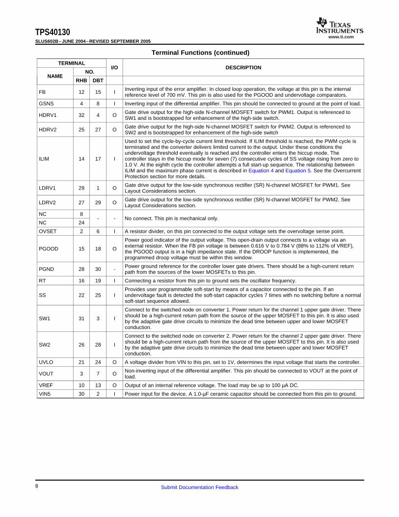
www.ti.comTPS40130SLUS602B–JUNE 2004–REVISED SEPTEMBER 2005
Terminal Functions (continued)
TERMINALI/O DESCRIPTION
NO.NAME
RHB DBT
Inverting input of the error amplifier. In closed loop operation, the voltage at this pin is the internalFB 12 15 I reference level of 700 mV. This pin is also used for the PGOOD and undervoltage comparators.
GSNS 4 8 I Inverting input of the differential amplifier. This pin should be connected to ground at the point of load.
Gate drive output for the high-side N-channel MOSFET switch for PWM1. Output is referenced toHDRV1 32 4 O SW1 and is bootstrapped for enhancement of the high-side switch.
Gate drive output for the high-side N-channel MOSFET switch for PWM2. Output is referenced toHDRV2 25 27 O SW2 and is bootstrapped for enhancement of the high-side switch
Used to set the cycle-by-cycle current limit threshold. If ILIM threshold is reached, the PWM cycle isterminated and the converter delivers limited current to the output. Under these conditions theundervoltage threshold eventually is reached and the controller enters the hiccup mode. The
ILIM 14 17 I controller stays in the hiccup mode for seven (7) consecutive cycles of SS voltage rising from zero to1.0 V. At the eighth cycle the controller attempts a full start-up sequence. The relationship betweenILIM and the maximum phase current is described in Equation 4 and Equation 5. See the OvercurrentProtection section for more details.
Gate drive output for the low-side synchronous rectifier (SR) N-channel MOSFET for PWM1. SeeLDRV1 29 1 O Layout Considerations section.
Gate drive output for the low-side synchronous rectifier (SR) N-channel MOSFET for PWM2. SeeLDRV2 27 29 O Layout Considerations section.
NC 8- - No connect. This pin is mechanical only.
NC 24
OVSET 2 6 I A resistor divider, on this pin connected to the output voltage sets the overvoltage sense point.
Power good indicator of the output voltage. This open-drain output connects to a voltage via anexternal resistor. When the FB pin voltage is between 0.616 V to 0.784 V (88% to 112% of VREF),PGOOD 15 18 O the PGOOD output is in a high impedance state. If the DROOP function is implemented, theprogrammed droop voltage must be within this window.
Power ground reference for the controller lower gate drivers. There should be a high-current returnPGND 28 30 - path from the sources of the lower MOSFETs to this pin.
RT 16 19 I Connecting a resistor from this pin to ground sets the oscillator frequency.
Provides user programmable soft-start by means of a capacitor connected to the pin. If anSS 22 25 I undervoltage fault is detected the soft-start capacitor cycles 7 times with no switching before a normal
soft-start sequence allowed.
Connect to the switched node on converter 1. Power return for the channel 1 upper gate driver. Thereshould be a high-current return path from the source of the upper MOSFET to this pin. It is also usedSW1 31 3 I by the adaptive gate drive circuits to minimize the dead time between upper and lower MOSFETconduction.
Connect to the switched node on converter 2. Power return for the channel 2 upper gate driver. Thereshould be a high-current return path from the source of the upper MOSFET to this pin. It is also usedSW2 26 28 I by the adaptive gate drive circuits to minimize the dead time between upper and lower MOSFETconduction.
UVLO 21 24 O A voltage divider from VIN to this pin, set to 1V, determines the input voltage that starts the controller.
Non-inverting input of the differential amplifier. This pin should be connected to VOUT at the point ofVOUT 3 7 O load.
VREF 10 13 O Output of an internal reference voltage. The load may be up to 100 µA DC.
VIN5 30 2 I Power input for the device. A 1.0-µF ceramic capacitor should be connected from this pin to ground.
8 Submit Documentation Feedback
www.ti.com
UDG−04030
Power-On Reset
U135 µA
23
22
10
11
U4PWM
LOGIC
18
BP5
AGND
CS1
CSRT1
FB
PWM1
TPS40130DBT
7
8
9
13
VOUT
GSNS
DIFFO
VREF
14
15
25
12
DROOP
FB
SS
COMP
21
20
17
24
CS2
CSRT2
ILIM
UVLO
16
19
6
EN/SYNC
RT
OVSET
+
+
+
U9ICTLR
U1
U7
U12
+U18
U11
+
0.7 V Ramp1U2
PWM2
U19OC/UVDetect
+
U3
+U15
PGOOD
U8
VIN5
BP5
U23Clock
U22Power−On Reset
U25OV Detect
U24Ramp Gen
Ramp1
Ramp2
U20SSUV
OV
OC29 LDRV2U21
U17 27 HDRV2
26 BOOT2
28 SW2
VIN5
1 LDRV1
2 VIN5
30 PGND
U10
U5Anti
CrossConduction
4 HDRV1
5 BOOT1
3 SW1
U6
U16Anti
CrossConduction
Ramp2U14
20 kΩ
20 kΩ
20 kΩ
20 kΩ
FUNCTIONAL DESCRIPTION
TPS40130SLUS602B–JUNE 2004–REVISED SEPTEMBER 2005
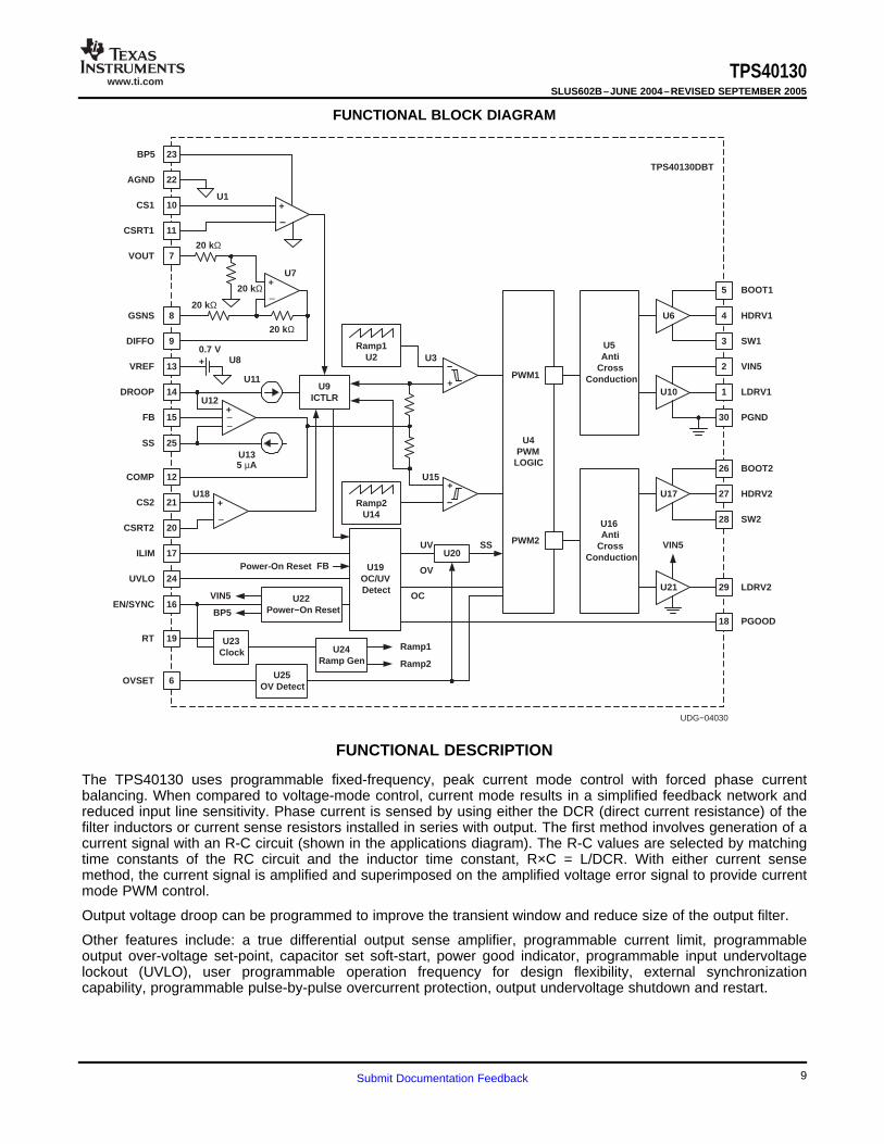
FUNCTIONAL BLOCK DIAGRAM
The TPS40130 uses programmable fixed-frequency, peak current mode control with forced phase currentbalancing. When compared to voltage-mode control, current mode results in a simplified feedback network andreduced input line sensitivity. Phase current is sensed by using either the DCR (direct current resistance) of thefilter inductors or current sense resistors installed in series with output. The first method involves generation of acurrent signal with an R-C circuit (shown in the applications diagram). The R-C values are selected by matchingtime constants of the RC circuit and the inductor time constant, R×C = L/DCR. With either current sensemethod, the current signal is amplified and superimposed on the amplified voltage error signal to provide currentmode PWM control.
Output voltage droop can be programmed to improve the transient window and reduce size of the output filter.
Other features include: a true differential output sense amplifier, programmable current limit, programmableoutput over-voltage set-point, capacitor set soft-start, power good indicator, programmable input undervoltagelockout (UVLO), user programmable operation frequency for design flexibility, external synchronizationcapability, programmable pulse-by-pulse overcurrent protection, output undervoltage shutdown and restart.
9Submit Documentation Feedback
www.ti.com
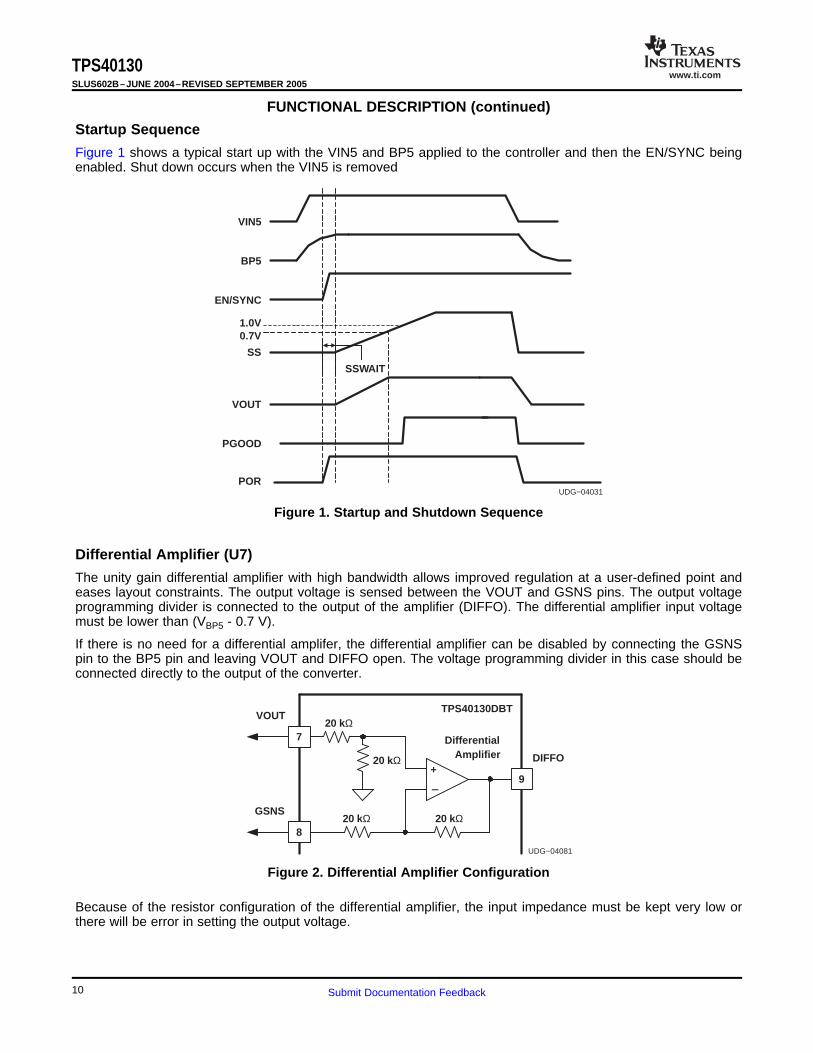
Startup Sequence
UDG−04031
EN/SYNC
BP5
VIN5
0.7V1.0V
VOUT
PGOOD
POR
SSWAIT
SS
Differential Amplifier (U7)
8
7
GSNS
DIFFO
VOUT
+
DifferentialAmplifier
TPS40130DBT
9
20 kΩ
20 kΩ
20 kΩ 20 kΩ
UDG−04081
TPS40130SLUS602B–JUNE 2004–REVISED SEPTEMBER 2005
FUNCTIONAL DESCRIPTION (continued)
Figure 1 shows a typical start up with the VIN5 and BP5 applied to the controller and then the EN/SYNC beingenabled. Shut down occurs when the VIN5 is removed
Figure 1. Startup and Shutdown Sequence
The unity gain differential amplifier with high bandwidth allows improved regulation at a user-defined point andeases layout constraints. The output voltage is sensed between the VOUT and GSNS pins. The output voltageprogramming divider is connected to the output of the amplifier (DIFFO). The differential amplifier input voltagemust be lower than (VBP5 - 0.7 V).
If there is no need for a differential amplifer, the differential amplifier can be disabled by connecting the GSNSpin to the BP5 pin and leaving VOUT and DIFFO open. The voltage programming divider in this case should beconnected directly to the output of the converter.
Figure 2. Differential Amplifier Configuration
Because of the resistor configuration of the differential amplifier, the input impedance must be kept very low orthere will be error in setting the output voltage.
10 Submit Documentation Feedback
www.ti.com
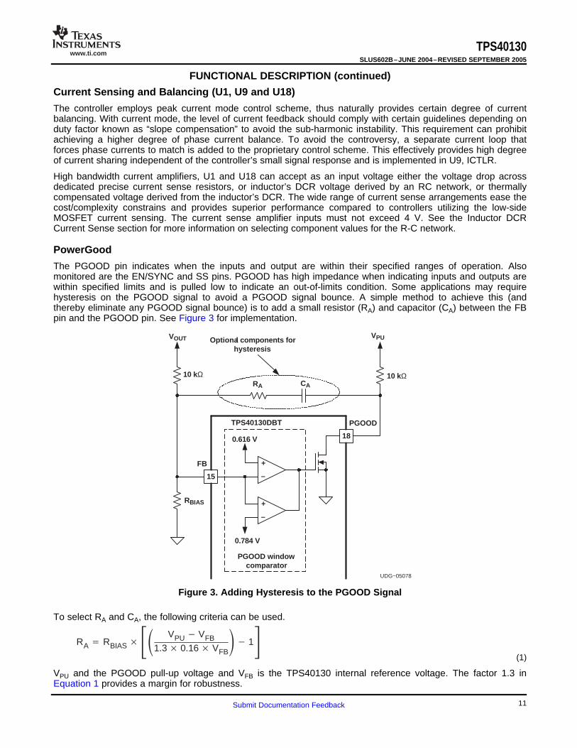
Current Sensing and Balancing (U1, U9 and U18)
PowerGood
15
18
+
+
TPS40130DBT
0.616 V
0.784 V
FB
PGOOD
PGOOD windowcomparator
Optional components forhysteresis
VOUT VPU
RA CA
RBIAS
10 kΩ 10 kΩ
UDG−05078
RA RBIAS VPU VFB1.3 0.16 VFB
1(1)
TPS40130SLUS602B–JUNE 2004–REVISED SEPTEMBER 2005
FUNCTIONAL DESCRIPTION (continued)
The controller employs peak current mode control scheme, thus naturally provides certain degree of currentbalancing. With current mode, the level of current feedback should comply with certain guidelines depending onduty factor known as “slope compensation” to avoid the sub-harmonic instability. This requirement can prohibitachieving a higher degree of phase current balance. To avoid the controversy, a separate current loop thatforces phase currents to match is added to the proprietary control scheme. This effectively provides high degreeof current sharing independent of the controller’s small signal response and is implemented in U9, ICTLR.
High bandwidth current amplifiers, U1 and U18 can accept as an input voltage either the voltage drop acrossdedicated precise current sense resistors, or inductor’s DCR voltage derived by an RC network, or thermallycompensated voltage derived from the inductor’s DCR. The wide range of current sense arrangements ease thecost/complexity constrains and provides superior performance compared to controllers utilizing the low-sideMOSFET current sensing. The current sense amplifier inputs must not exceed 4 V. See the Inductor DCRCurrent Sense section for more information on selecting component values for the R-C network.
The PGOOD pin indicates when the inputs and output are within their specified ranges of operation. Alsomonitored are the EN/SYNC and SS pins. PGOOD has high impedance when indicating inputs and outputs arewithin specified limits and is pulled low to indicate an out-of-limits condition. Some applications may requirehysteresis on the PGOOD signal to avoid a PGOOD signal bounce. A simple method to achieve this (andthereby eliminate any PGOOD signal bounce) is to add a small resistor (RA) and capacitor (CA) between the FBpin and the PGOOD pin. See Figure 3 for implementation.
Figure 3. Adding Hysteresis to the PGOOD Signal
To select RA and CA, the following criteria can be used.
VPU and the PGOOD pull-up voltage and VFB is the TPS40130 internal reference voltage. The factor 1.3 inEquation 1 provides a margin for robustness.
11Submit Documentation Feedback
www.ti.com
CA 100 nsRA (2)
Soft-Start
tSS 0.7 CSS
5 106 (3)
Overcurrent Protection
VILIM 2.7 IPH(max) RCS (4)
IPH(max) IOUT
2
VIN VOUT VOUT
2 LOUT fSW VIN (5)
Current Sense Fault Protection
TPS40130SLUS602B–JUNE 2004–REVISED SEPTEMBER 2005
FUNCTIONAL DESCRIPTION (continued)
Even though CA may calculate to less than 1 pF, a capacitance of no more than 4.7 pF is recommended.
A capacitor connected to the soft start pin (SS) sets the power-up time. When EN is high and POR is cleared,the calibrated current source, U13, starts charging the external soft start capacitor. The PGOOD pin is held lowduring the start up. The rising voltage across the capacitor serves as a reference for the error amplifier, U12.When the soft-start voltage reaches the level of the reference voltage, U8 (VVREF=0.7V), the converter’s outputreaches the regulation point and further voltage rise of the soft start voltage has no effect on the output. Whenthe soft start voltage reaches 1.0 V, the power good (PGOOD) function is cleared to be reported on the PGOODpin. Normally the PGOOD pin goes high at this time. Equation 3 is used to calculate the value of the soft-startcapacitor.
The overcurrent function, U19, monitors the output of current sense amplifiers U1 and U18. These currents areconverted to voltages and compared to the voltage on the ILIM pin. The relationship between the maximumphase current and the current sense resistance is given in the following equation. In case a threshold of VILIM/2.7is exceeded the PWM cycle on the associated phase is terminated. The overcurrent threshold, IPH(max), and thevoltage to set on the ILIM pin is determined by Equation 4 and Equation 5.
where• IPH(max) is a maximum value of the phase current allowed• IOUT is the total maximum DC output current• RCS is a value of the current sense resistor used or the DCR value of the output inductor, LOUT
If the overcurrent condition persists, both phases have PWM cycles terminated by the overcurrent signals. Thisputs a converter in a constant current mode with the output current programmed by the ILIM voltage. Eventuallythe supply-and-demand equilibrium on the converter output is not satisfied and the output voltage starts todecline. When the undervoltage threshold is reached, the converter enters a hiccup mode. The controller isstopped and the output is not regulated any more, the soft-start pin function changes.
It now serves as a hiccup timing capacitor controlled by U20, the fault control circuit. The soft-start pin isperiodically charged and discharged by U20. After seven hiccup cycles, the controller attempts another soft-startcycle to restore normal operation. If the overload condition persists, the controller returns to the hiccup mode.This condition may continue indefinitely. In such conditions the average current delivered to the load isapproximately 1/8 of the set overcurrent value.
Multiphase controllers with forced current sharing are inherently sensitive to a failure of the current sensecomponent or a defect in the assembly process. In case of such failure the entire load current can be steeredwith catastrophic consequences into a single channel where the fault has occurred. A dedicated circuit in theTPS40130 controller detects this defect and prevents the controller from starting up. This fault detection circuit isactive only during chip initialization and does not protect should current sense failure happen during normaloperation.
12 Submit Documentation Feedback
www.ti.com
Overvoltage Protection
Output Undervoltage Protection
Programmable Input Undervoltage Lockout Protection
Power-On Reset (POR)
Fault Masking Operation
Fault Conditions and MOSFET Control
TPS40130SLUS602B–JUNE 2004–REVISED SEPTEMBER 2005
FUNCTIONAL DESCRIPTION (continued)
After the device is enabled and prior to the IC starting (during the first 32 clock cycles), a 5-µA current flows outof the CS1 and CS2 pins. The current flows through the external components: current sense resistor, RCS, theoutput inductor and the output capacitor(s) to ground. If the voltage on the CS1 and CS2 pins exceed 0.2 V(resistance greater than 40 kΩ), a fault is declared and the device does not start. This is a fault detection featurethat insures the output inductor, current sense resistor and output capacitors are installed properly on the board.
The voltage on OVSET is compared with 0.817 V, 16% higher than VREF, in U25 to determine the outputovervoltage point. When an overvoltage is detected, the output drivers command the upper MOSFETs off andthe lower MOSFETs on. If the overvoltage is caused by a shorted upper MOSFET, latching on the lowerMOSFET should blow the input fuse and protect the output. Hiccup mode consisting of seven (7) soft-starttiming cycles is initiated and then attempts to restart. If the overvoltage condition has been cleared and the inputfuse has not opened, the output comes up and normal operation continues. If the overvoltage condition persists,the controller restarts to allow the output to rise to the overvoltage level and return to the hiccup mode. Using avoltage divider with the same ratio, that sets the output voltage, an output overvoltage is declared when theoutput rises 16% above nominal.
If the output voltage, as sensed by U19 on the FB pin becomes less than 0.588 V, the undervoltage protectionthreshold (84% of VREF), the controller enters the hiccup mode as it is described in the Overcurrent Protectionsection.
A voltage divider that sets 1V on the UVLO pin determines when the controller starts operating. Operationcommences when the voltage on the UVLO pin exceeds 1.0 V.
The power-on reset (POR) function, U22, insures the VIN5 and BP5 voltages are within their regulation windowsbefore the controller is allowed to start.
If the SS pin voltage is externally limited below the 1-V threshold, the controller does not respond to most faultsand the PGOOD output is always low. Only the overcurrent function and current sense fault remain active. Theovercurrent protection still continues to terminate PWM cycle every time when the threshold is exceeded but thehiccup mode is not entered.
Table 1 shows a summary of the fault conditions and the state of the MOSFETs.
Table 1. Fault Condifions
FAULT MODE UPPER MOSFET LOWER MOSFET
EN/SYNC = LOW OFF OFF
FIXED UVLO, VBP5 < 4.25 V OFF OFF
Programmable UVLO, < 1.0 V OFF ON
Output undervoltage OFF, Hiccup mode ON, Hiccup mode
Output overvoltage OFF, Hiccup mode ON, Hiccup mode
ISF, current sense fault OFF ON
13Submit Documentation Feedback
www.ti.com
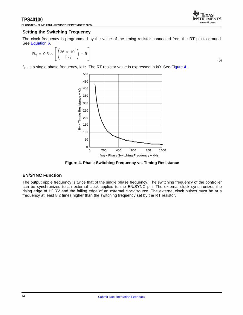
Setting the Switching Frequency
RT 0.8 36 103
fPH 9
(6)
fSW − Phase Switching Frequency − kHz
RT
− Ti
min
g R
esis
tanc
e −
kΩ
00 1000200 400 600 800
50
100
150
200
250
300
350
400
450
500
EN/SYNC Function
TPS40130SLUS602B–JUNE 2004–REVISED SEPTEMBER 2005
The clock frequency is programmed by the value of the timing resistor connected from the RT pin to ground.See Equation 6.
fPH is a single phase frequency, kHz. The RT resistor value is expressed in kΩ. See Figure 4.
Figure 4. Phase Switching Frequency vs. Timing Resistance
The output ripple frequency is twice that of the single phase frequency. The switching frequency of the controllercan be synchronized to an external clock applied to the EN/SYNC pin. The external clock synchronizes therising edge of HDRV and the falling edge of an external clock source. The external clock pulses must be at afrequency at least 8.2 times higher than the switching frequency set by the RT resistor.
14 Submit Documentation Feedback
www.ti.com
Setting Overcurrent Protection
VILIM 2.7 IPH(max) RCS (7)
IPH(max) IOUT
2
VIN VOUT VOUT
2 LOUT fSW VIN (8)
Resistor Divider Calculation for VOUT, ILIM, OVSET and UVLO
RBIAS 0.7 R1VOUT 0.7 (9)
R6 R5 VILIM
0.7 VILIM
(10)
R4 0.812 R3VOUT(ov) 0.812
(11)
R8 1.0 R7VIN 1.0 (12)
Feedback Loop Compensation
fOP 12 ROUT COUT (13)
fESRZ 12 RESR COUT (14)
TPS40130SLUS602B–JUNE 2004–REVISED SEPTEMBER 2005
Setting the overcurrent protection is given in the following equations. Care must be taken when calculating VILIMto include the increase in RCS caused by the output current as it approaches the overcurrent trip point. The DCR(RCS in the equation) of the inductor increases approximately 0.39% per degree Centigrade.
where• IPH(max) is a maximum value of the phase current allowed• IOUT is the total maximum DC output current• LOUT is the output inductor value• fSW is the switching frequency• VOUT is the output voltage• VIN is the input voltage• RCS is a value of the current sense resistor used or the DCR value of the output inductor, LOUT
Use Figure 9 for setting the output voltage, current limit voltage and overvoltage setting voltage. Select RBIASusing Equation 9. With a voltage divider from VREF, select R6 using Equation 10. WIth a voltage from DIFFOselect R4 using Equation 11. With a voltage divider from VIN, select R8 using Equation 12.
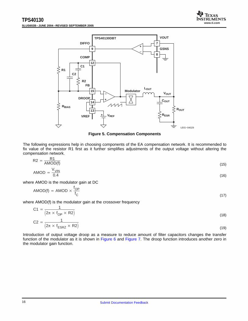
The TPS40130 operates in a peak-current mode and the converter exhibits a single pole response with ESRzero for which Type II compensation network is usually adequate as shown in Figure 5.
The load pole is situated at a value calculated using Equation 13.
and the ESR zero is situated at a value calculated using Equation 14.
To achieve the desired bandwidth the error amplifier has to compensate for modulator gain loss at the crossoverfrequency. A zero placed at the load pole frequency facilitates that. The ESR zero alters the modulator -1 slopeat higher frequencies. To compensate for the ESR zero, a pole in the error amplifier transfer function should beplaced at the ESR zero frequency.
15Submit Documentation Feedback
www.ti.com
C1
R2
C2
15
+7
8
+14
13+
12
9
R1
Modulator
DIFFO
COMP
FB
DROOP
VREF
VOUT
GSNS
LOUT
VOUT
COUT
RESR
ROUT
VREF
RBIAS
UDG−04029
TPS40130DBT
R2 R1AMOD(f) (15)
AMOD VVIN0.4 (16)
AMOD(f) AMOD fOPfC (17)
C1 12 fOP R2 (18)
C2 12 fESRZ R2 (19)
TPS40130SLUS602B–JUNE 2004–REVISED SEPTEMBER 2005
Figure 5. Compensation Components
The following expressions help in choosing components of the EA compensation network. It is recommended tofix value of the resistor R1 first as it further simplifies adjustments of the output voltage without altering thecompensation network.
where AMOD is the modulator gain at DC
where AMOD(f) is the modulator gain at the crossover frequency
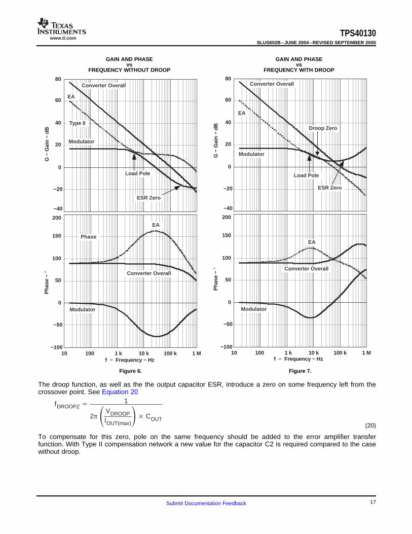
Introduction of output voltage droop as a measure to reduce amount of filter capacitors changes the transferfunction of the modulator as it is shown in Figure 6 and Figure 7. The droop function introduces another zero inthe modulator gain function.
16 Submit Documentation Feedback
www.ti.com
200
−40
−20
0
20
40
60
80
−100
−50
0
50
100
150
10 100 1 k 10 k 100 k 1 M
G −
Gai
n −
dBP
hase
− °
f − Frequency − Hz
ESR Zero
Load Pole
Droop Zero
Modulator
Converter Overall
EA
Modulator
Converter Overall
EA
200
10
−40
100 1 k 10 k 100 k 1 M
−20
0
20
40
60
80
−100
−50
0
50
100
150
f − Frequency − Hz
G −
Gai
n −
dBP
hase
− °
Modulator
Phase
Converter Overall
EA
Type II
ESR Zero
Load Pole
Modulator
Converter Overall
EA
fDROOPZ 1
2 VDROOPIOUT(max)
COUT(20)
TPS40130SLUS602B–JUNE 2004–REVISED SEPTEMBER 2005
GAIN AND PHASE GAIN AND PHASEvs vs
FREQUENCY WITHOUT DROOP FREQUENCY WITH DROOP
Figure 6. Figure 7.
The droop function, as well as the the output capacitor ESR, introduce a zero on some frequency left from thecrossover point. See Equation 20
To compensate for this zero, pole on the same frequency should be added to the error amplifier transferfunction. With Type II compensation network a new value for the capacitor C2 is required compared to the casewithout droop.
17Submit Documentation Feedback
www.ti.com
C2 C12 R2 C1 fDROOPZ 1 (21)
G −
Gai
n −
dB
Pha
se −
°
f − Frequency − Hz
60
0
10
20
40
50
30
−20
−10
0
60
80
20
40
−20100 1 k 10 k 100 k 1 M
Phase
Gain
VIN = 12 VVOUT = 1.5 V
Setting the Output Voltage Droop
RDROOP 5000 VDROOP
IOUT RCS
RBIASR1 RBIAS (22)
TPS40130SLUS602B–JUNE 2004–REVISED SEPTEMBER 2005
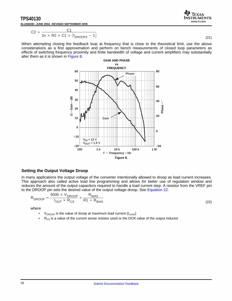
When attempting closing the feedback loop at frequency that is close to the theoretical limit, use the aboveconsiderations as a first approximation and perform on bench measurements of closed loop parameters aseffects of switching frequency proximity and finite bandwidth of voltage and current amplifiers may substantiallyalter them as it is shown in Figure 8.
GAIN AND PHASEvs
FREQUENCY
Figure 8.
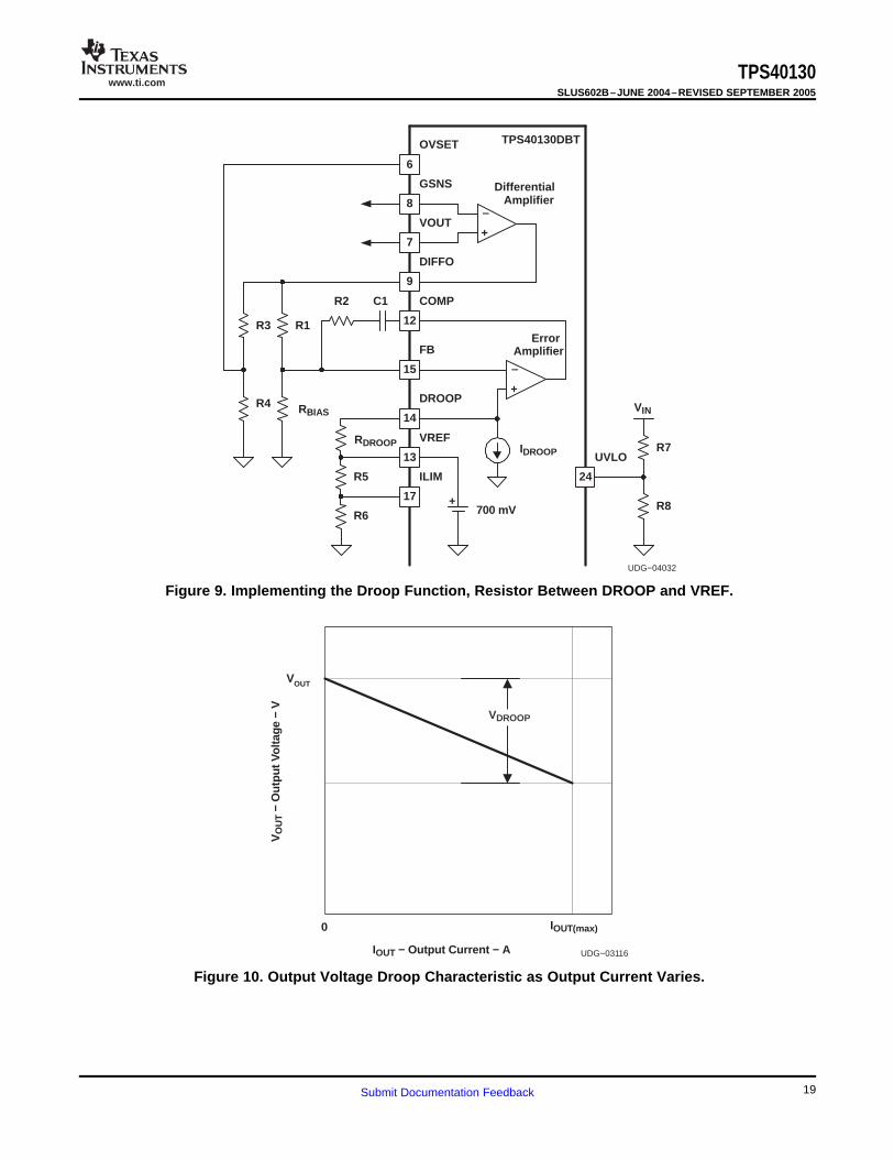
In many applications the output voltage of the converter intentionally allowed to droop as load current increases.This approach also called active load line programming and allows for better use of regulation window andreduces the amount of the output capacitors required to handle a load current step. A resistor from the VREF pinto the DROOP pin sets the desired value of the output voltage droop. See Equation 22.
where• VDROOP is the value of droop at maximum load current (ILOAD)• RCS is a value of the current sense resistor used or the DCR value of the output inductor
18 Submit Documentation Feedback
www.ti.com
8
7
9
12
GSNS
DIFFO
VOUT
VREF
15
14
13
COMP
FB
DROOP
+
+
700 mV
ErrorAmplifier
DifferentialAmplifier
17
ILIM
6
OVSET TPS40130DBT
+
24
UVLO
C1R2
R1
R5
R6
R7
R8
R3
R4
IDROOPRDROOP
RBIAS VIN
UDG−04032
IOUT − Output Current − A
VO
UT
− O
utpu
t Vol
tage
− V
0
VOUT
IOUT(max)
VDROOP
UDG−03116
TPS40130SLUS602B–JUNE 2004–REVISED SEPTEMBER 2005
Figure 9. Implementing the Droop Function, Resistor Between DROOP and VREF.
Figure 10. Output Voltage Droop Characteristic as Output Current Varies.
19Submit Documentation Feedback
www.ti.com
Inductor DCR Current Sense
VDCR VIN VOUT DCR
DCR L (23)
VC VIN VOUT 1
C RCS 1C
(24)
VC 1
C RCS 1C
DCR
DCR L; L
DCR RCS C; DCRL RC
(25)
VOUT
VC
SwitchNode
UDG−03142
LDCR
C
VDCR
RCS
CS CSRT
C
LDCR
CSRTCS
R0.1%
R0.1%
R0.1%
R0.1%
UDG−05079
RCS
VDCR
SwitchNode
VOUT
VC
Inductor DCR Current Sensing with 5-V Outputs
TPS40130SLUS602B–JUNE 2004–REVISED SEPTEMBER 2005
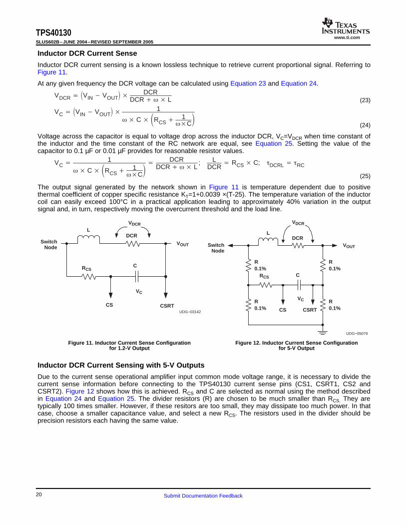
Inductor DCR current sensing is a known lossless technique to retrieve current proportional signal. Referring toFigure 11.
At any given frequency the DCR voltage can be calculated using Equation 23 and Equation 24.
Voltage across the capacitor is equal to voltage drop across the inductor DCR, VC=VDCR when time constant ofthe inductor and the time constant of the RC network are equal, see Equation 25. Setting the value of thecapacitor to 0.1 µF or 0.01 µF provides for reasonable resistor values.
The output signal generated by the network shown in Figure 11 is temperature dependent due to positivethermal coefficient of copper specific resistance KT=1+0.0039 ×(T-25). The temperature variation of the inductorcoil can easily exceed 100°C in a practical application leading to approximately 40% variation in the outputsignal and, in turn, respectively moving the overcurrent threshold and the load line.
Figure 11. Inductor Current Sense Configuration Figure 12. Inductor Current Sense Configurationfor 1.2-V Output for 5-V Output
Due to the current sense operational amplifier input common mode voltage range, it is necessary to divide thecurrent sense information before connecting to the TPS40130 current sense pins (CS1, CSRT1, CS2 andCSRT2). Figure 12 shows how this is achieved. RCS and C are selected as normal using the method describedin Equation 24 and Equation 25. The divider resistors (R) are chosen to be much smaller than RCS. They aretypically 100 times smaller. However, if these resitors are too small, they may dissipate too much power. In thatcase, choose a smaller capacitance value, and select a new RCS. The resistors used in the divider should beprecision resistors each having the same value.
20 Submit Documentation Feedback
www.ti.com
APPLICATION INFORMATION
Applications Circuit
1
2
3
4
30
29
28
27
PGND
LDRV2
SW2
HDRV2
LDRV1
VIN5
SW1
HDRV1
TPS40130DBT
5
6
7
8
BOOT1
OVSET
VOUT
GSNS
9
10
11
DIFFO
CS1
CSRT1
12
13
14
15
COMP
VREF
DROOP
FB
26
25
24
23
BOOT2
SS
UVLO
BP5
22
21
20
19
AGND
CS2
CSRT2
RT
18
17
16
PGOOD
ILIM
EN/SYNC 5 V
VREF
R6
R7
12 V
C7 2200 pF
L2
R1C4
D1BAT54A
D2
5 V
L1
R2 C5
12 V
12 V
DIFFO
R11C8
C17 C15Q2
Q5,Q6
PGND
C20
C19
C21 C12C13Q1
Q3,Q4
PGND
C10
FB
R19 EN/SYNC
5 V
LOAD
UDG−04018
R18
R17
R5 90.9 kΩ
R8 10 kΩ
R16 10 kΩ
C60.1 µF
R2210 Ω
VOUT
C10.1 µF
R1310 kΩ
R1410 kΩ
R1010 kΩ
R21 51 Ω
R20 51 Ω
R12 10 kΩC90.1 µF
VOUT
C20.1 µF
1.0 Ω
1.0 Ω
VOUT
TPS40130SLUS602B–JUNE 2004–REVISED SEPTEMBER 2005
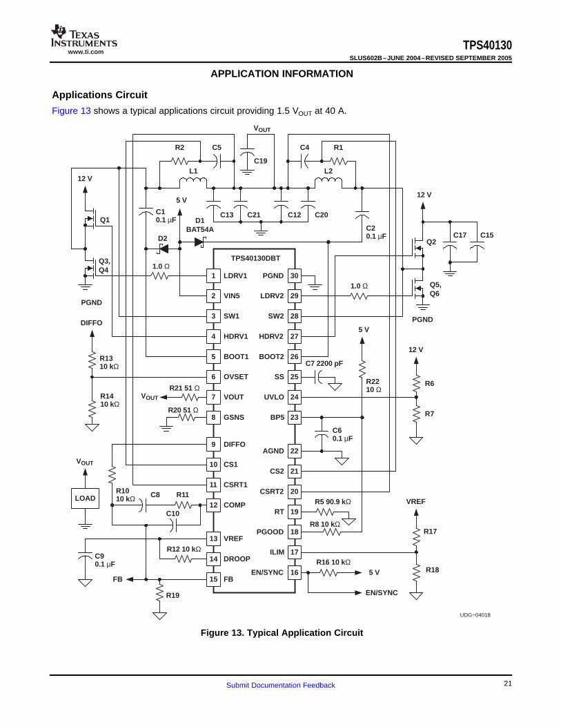
Figure 13 shows a typical applications circuit providing 1.5 VOUT at 40 A.
Figure 13. Typical Application Circuit
21Submit Documentation Feedback
www.ti.com
Additional Application Circuits
1
2
3
4
30
29
28
27
PGND
LDRV2
SW2
HDRV2
LDRV1
VIN5
SW1
HDRV1
TPS40130DBT
5
6
7
8
BOOT1
OVSET
VOUT
GSNS
9
10
11
DIFFO
CS1
CSRT1
12
13
14
15
COMP
VREF
DROOP
FB
26
25
24
23
BOOT2
SS
UVLO
BP5
22
21
20
19
AGND
CS2
CSRT2
RT
18
17
16
PGOOD
ILIM
EN/SYNC
R17
R185 V
R6
R7
12 V
C7 2200 pF
L2
R1C4
D1BAT54A
D2
5 V
L1
R2 C5
12 V
12 V
R11C8
C17 C15Q2
Q5,Q6
PGND
C20
C19
C21 C12C13Q1
Q3,Q4
PGND
C10
FB
EN/SYNC
5 V
BP5
SS
8
1
2
3
14
9
10
12
VCC
FB
BIAS
NCPU1
VOUT
VID5
VID0
VID1
4
5
6
7
VID2
VID3
VID4
GND
13NCPU2
TPS40120
11N/C
DIFFO
UDG−04088
C90.1 µF
R12 10 ΩR16 10 kΩ
R8 10 kΩ
R5 90.9 kΩ
C60.1 µF
R2210 Ω
C20.1 µF
VOUT
R1310 kΩ
R1410 kΩ VOUT
C10.1 µF
1.0 Ω
R21 51 Ω
R20 51 Ω
1.0 Ω
VREF
TPS40130SLUS602B–JUNE 2004–REVISED SEPTEMBER 2005
APPLICATION INFORMATION (continued)
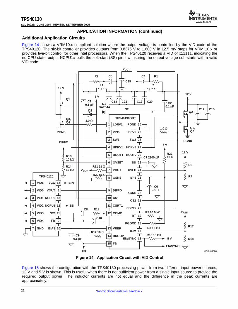
Figure 14 shows a VRM10.x compliant solution where the output voltage is controlled by the VID code of theTPS40120. The six-bit controller provides outputs from 0.8375 V to 1.600 V in 12.5 mV steps for VRM 10.x orprovides five-bit control for other Intel processors. When the TPS40120 receives a VID of x11111, indicating theno CPU state, output NCPU1# pulls the soft-start (SS) pin low insuring the output voltage soft-starts with a validVID code.
Figure 14. Application Circuit with VID Control
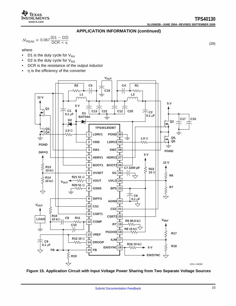
Figure 15 shows the configuration with the TPS40130 processing power from two different input power sources,12 V and 5 V is shown. This is useful when there is not sufficient power from a single input source to provide therequired output power. The inductor currents are not equal and the difference in the peak currents areapproximately:
22 Submit Documentation Feedback
www.ti.com
IPEAK 0.067(D1 D2)DCR (26)
1
2
3
4
30
29
28
27
PGND
LDRV2
SW2
HDRV2
LDRV1
VIN5
SW1
HDRV1
TPS40130DBT
5
6
7
8
BOOT1
OVSET
VOUT
GSNS
9
10
11
DIFFO
CS1
CSRT1
12
13
14
15
COMP
VREF
DROOP
FB
26
25
24
23
BOOT2
SS
UVLO
BP5
22
21
20
19
AGND
CS2
CSRT2
RT
18
17
16
PGOOD
ILIM
EN/SYNC
R17
R185 V
R6
R7
12 V
C7 2200 pF
L2
R1C4
D1BAT54A
D2
5 V
L1
R2 C5
5 V
12 V
DIFFO
R11C8
C17 C15Q2
Q5,Q6
PGND
C20
C19
C21 C12C13Q1
Q3,Q4
PGND
C10
FB
R19 EN/SYNC
5 V
LOAD
UDG−04089
C90.1 µF
R12 10 Ω
R16 10 kΩ
R8 10 kΩ
R5 90.9 kΩ
C60.1 µF
R2210 Ω
C20.1 µF
VOUT
R1310 kΩ
R1410 kΩ VOUT
C10.1 µF
1.0 Ω
R21 51 Ω
R20 51 Ω
1.0 Ω
R1010 kΩ VREF
VOUT
TPS40130SLUS602B–JUNE 2004–REVISED SEPTEMBER 2005
APPLICATION INFORMATION (continued)
where• D1 is the duty cycle for VIN1
• D2 is the duty cycle for VIN2
• DCR is the resistance of the output inductor• η is the efficiency of the converter
Figure 15. Application Circuit with Input Voltage Power Sharing from Two Separate Voltage Sources
23Submit Documentation Feedback
www.ti.com
1
2
3
4
24
23
22
21
NC
BOOT2
SS
UVLO
BOOT1
OVSET
VOUT
GSNS
5 20BP5DIFFO
6
7
8
CS1
CSRT1
NC
32 31 30 29 28 27 26 25
HD
RV
1
SW
1
VIN
5
LD
RV
1
PG
ND
LD
RV
2
SW
2
HD
RV
2
19
18
17
AGND
CS2
CSRT2
9 10 11 12 15 16
CO
MP
VR
EF
DR
OO
P
FB
EN
/SY
NC
ILIM
PG
OO
D
RT
D2BAT54A
C7 2200 pF
C4
R17
R18
C8R11
R12
C10 R19
C5
R6
R7
R1
L2
TPS40130RHB
12 V5 V
C19 C20
C21C12 C13
L1
Q6Q5
Q4Q3
Q2
D1BAT54A
C17
C15
Q1
TL431
R2
12 V
VREF
R810 kΩ
C190.1 µF
R1610 kΩ
R590.9 kΩ
1 Ω
C60.1 µF
R2210 Ω
C20.1 µF
1 Ω
VOUT
VOUT
R1010 kΩ
R1310 kΩ
R21 51 Ω
R22 51 Ω
C10.1 µF
10 kΩ
10 kΩ
115 Ω
UDG−05080
R1410 kΩ
13 14
5 V
EN/SYNC
TPS40130SLUS602B–JUNE 2004–REVISED SEPTEMBER 2005
APPLICATION INFORMATION (continued)
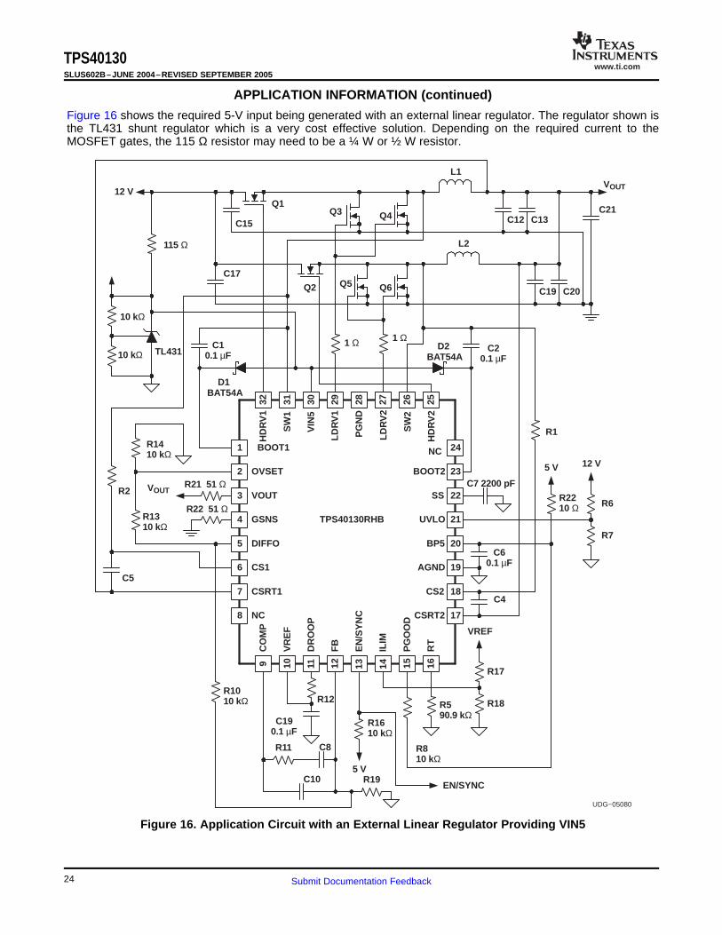
Figure 16 shows the required 5-V input being generated with an external linear regulator. The regulator shown isthe TL431 shunt regulator which is a very cost effective solution. Depending on the required current to theMOSFET gates, the 115 Ω resistor may need to be a ¼ W or ½ W resistor.
Figure 16. Application Circuit with an External Linear Regulator Providing VIN5
24 Submit Documentation Feedback
www.ti.com
UDG−04091
C90.1 µF
R12 10 Ω
R16 10 kΩ
R8 10 kΩ
R5 33.2 kΩ
C60.1 µF
R2210 Ω
C20.1 µF
VOUT
R1310 kΩ
VOUT
C10.1 µF
1.0 Ω
R21 51 Ω
R20 51 Ω
1.0 Ω
R1010 kΩ
R1410 kΩ
1
2
3
4
30
29
28
27
PGND
LDRV2
SW2
HDRV2
LDRV1
VIN5
SW1
HDRV1
TPS40130DBT
5
6
7
8
BOOT1
OVSET
VOUT
GSNS
9
10
11
DIFFO
CS1
CSRT1
12
13
14
15
COMP
VREF
DROOP
FB
26
25
24
23
BOOT2
SS
UVLO
BP5
22
21
20
19
AGND
CS2
CSRT2
RT
18
17
16
PGOOD
ILIM
EN/SYNC
R17
R185 V
VREF
R6
R7
5 V
C7 2200 pF
L2
R1C4
D1BAT54A
D2
5 V
L1
R2 C5
5 V
5 V
DIFFO
R11C8
C17 C15Q2
Q5,Q6
PGND
C20
C19
C21 C12C13Q1
Q3,Q4
PGND
C10
FB
R19 EN/SYNC
5 V
LOAD
VOUT
TPS40130SLUS602B–JUNE 2004–REVISED SEPTEMBER 2005
APPLICATION INFORMATION (continued)
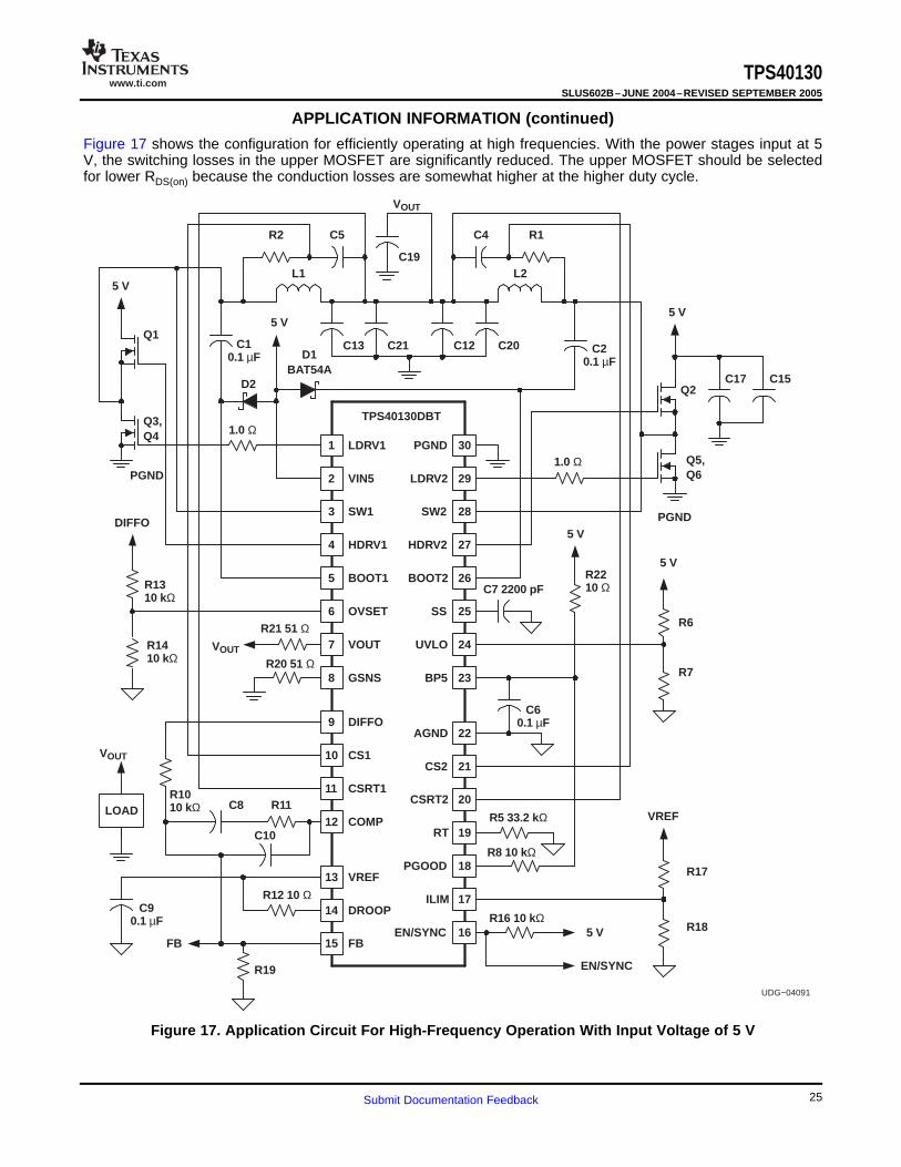
Figure 17 shows the configuration for efficiently operating at high frequencies. With the power stages input at 5V, the switching losses in the upper MOSFET are significantly reduced. The upper MOSFET should be selectedfor lower RDS(on) because the conduction losses are somewhat higher at the higher duty cycle.
Figure 17. Application Circuit For High-Frequency Operation With Input Voltage of 5 V
25Submit Documentation Feedback
www.ti.com
1
2
3
4
30
29
28
27
PGND
LDRV2
SW2
HDRV2
LDRV1
VIN5
SW1
HDRV1
TPS40130DBT
5
6
7
8
BOOT1
OVSET
VOUT
GSNS
9
10
11
DIFFO
CS1
CSRT1
12
13
14
15
COMP
VREF
DROOP
FB
26
25
24
23
BOOT2
SS
UVLO
BP5
22
21
20
19
AGND
CS2
CSRT2
RT
18
17
16
PGOOD
ILIM
EN/SYNC
R17
R185 V
C7 2200 pF
L2
D2BAT54A
5 V
L1
12 V
12 V
R11C8
C17Q2
Q5, Q6
PGND
C20C19C21 C12C13Q1
Q3, Q4
C10
FB
EN/SYNC
5 V
LOAD
R350.1 %
R440.1%
R430.1%
BP5
R1
C4
R340.1%
D1 BAT54AC15
R330.1 % R2
C5
R420.1 %
R320.1 %
R400.1 %
C20.1 µF
R191.62 kΩ
VOUT
C90.1 µF
R12 10 Ω
R1010 kΩ
R1410 kΩ
R2210 kΩ
R16 10 kΩ
R8 10 kΩ
R5 90.9 kΩ
C60.1 µF
1.0 Ω
VOUT
R1310 kΩ
1.0 Ω
C10.1 µF
VREF
UDG−04092
VOUT
TPS40130SLUS602B–JUNE 2004–REVISED SEPTEMBER 2005
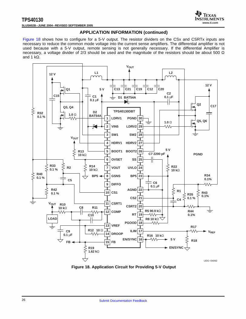
APPLICATION INFORMATION (continued)
Figure 18 shows how to configure for a 5-V output. The resistor dividers on the CSx and CSRTx inputs arenecessary to reduce the common mode voltage into the current sense amplifiers. The differential amplifier is notused because with a 5-V output, remote sensing is not generally necessary. If the differential Amplifier isnecessary, a voltage divider of 2/3 should be used and the magnitude of the resistors should be about 500 Ωand 1 kΩ.
Figure 18. Application Circuit for Providing 5-V Output
26 Submit Documentation Feedback
www.ti.com
TYPICAL CHARACTERISTRICS
IL1, IL2(5 A/div)
t − Time − 20 µs/div
VDIFFOUT(50 mV/div)
VSW2 (10 V / div)
VDIFFOUT (50 mV/div)
IL2 (5 A / div)
IL1 (5 A / div)
t − Time − 4 µs/div
VSW2 (10 V / div)
VSW1 (10 V/div)
VDIFFOUT (500 mV/div)
VSS (100 mV / div)
t − Time − 40 µs/div
VEN/SYNC (5 V / div)
VDIFFOUT (50 mV/div)
IL2 (5 A / div)
IL1 (5 A / div)
t − Time − 4 µs/div
VSW2 (10 V / div)
TPS40130SLUS602B–JUNE 2004–REVISED SEPTEMBER 2005
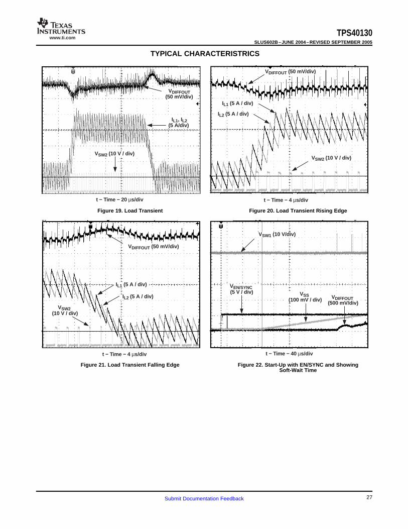
Figure 19. Load Transient Figure 20. Load Transient Rising Edge
Figure 21. Load Transient Falling Edge Figure 22. Start-Up with EN/SYNC and ShowingSoft-Wait Time
27Submit Documentation Feedback
www.ti.com
VDIFFOUT (500 mV/div)
t − Time − 400 µs/div
VEN/SYNC (5 V / div)
VSS (500 mV / div)
VEN/SYNC (5 V/div)
t − Time − 400 ns/div
VHDRV2 (10 V / div)
VHDRV1 (10 V / div)
VEN/SYNC (5 V/div)
t − Time − 40 ns/div
VHDRV2(10 V / div)
VHDRV1(10 V / div)
t − Time − 4 ms/div
VOVSET(1 V / div)
VLDRV1(5 V / div)
VSS (500 mV / div)
TPS40130SLUS602B–JUNE 2004–REVISED SEPTEMBER 2005
TYPICAL CHARACTERISTRICS (continued)
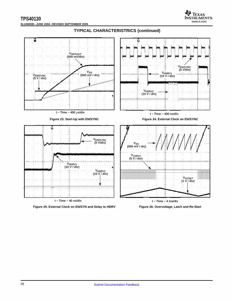
Figure 23. Start-Up with EN/SYNC Figure 24. External Clock on EN/SYNC
Figure 25. External Clock on EN/SYN and Delay to HDRV Figure 26. Overvoltage, Latch and Re-Start
28 Submit Documentation Feedback
www.ti.com
t − Time − 4 ms/div
VSS (1 V/ div)
VFB (200 mV / div)
IL2, IL2 (10 A / div)
VSS (1 V/div)
VFB (200 mV/ div)
VFB = 0.588 V
t − Time − 40 µs/div
IL2, IL2 (10 A / div)
LAYOUT CONSIDERATIONS
Introduction
Two Ground Planes
Low-Level Signal Connections and Routing
Current Sense Signals
TPS40130SLUS602B–JUNE 2004–REVISED SEPTEMBER 2005
TYPICAL CHARACTERISTRICS (continued)
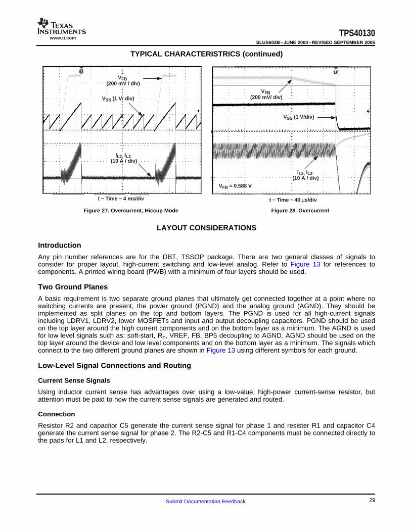
Figure 27. Overcurrent, Hiccup Mode Figure 28. Overcurrent
Any pin number references are for the DBT, TSSOP package. There are two general classes of signals toconsider for proper layout, high-current switching and low-level analog. Refer to Figure 13 for references tocomponents. A printed wiring board (PWB) with a minimum of four layers should be used.
A basic requirement is two separate ground planes that ultimately get connected together at a point where noswitching currents are present, the power ground (PGND) and the analog ground (AGND). They should beimplemented as split planes on the top and bottom layers. The PGND is used for all high-current signalsincluding LDRV1, LDRV2, lower MOSFETs and input and output decoupling capacitors. PGND should be usedon the top layer around the high current components and on the bottom layer as a minimum. The AGND is usedfor low level signals such as: soft-start, RT, VREF, FB, BP5 decoupling to AGND. AGND should be used on thetop layer around the device and low level components and on the bottom layer as a minimum. The signals whichconnect to the two different ground planes are shown in Figure 13 using different symbols for each ground.
Using inductor current sense has advantages over using a low-value, high-power current-sense resistor, butattention must be paid to how the current sense signals are generated and routed.
Connection
Resistor R2 and capacitor C5 generate the current sense signal for phase 1 and resister R1 and capacitor C4generate the current sense signal for phase 2. The R2-C5 and R1-C4 components must be connected directly tothe pads for L1 and L2, respectively.
29Submit Documentation Feedback
www.ti.com
Differential Amplifier Signals
High-Current Connections and Routing
Device Decoupling for VIN5 and BP5
Symmetry
SW Node
Lower MOSFET Gate Drive, LDRV1 and LDRV2
Upper MOSFET Gate Drive, HDRV1 and HDRV2
TPS40130SLUS602B–JUNE 2004–REVISED SEPTEMBER 2005
LAYOUT CONSIDERATIONS (continued)Routing
The traces that connect to C5 and C4 should be made directly at the capacitor(s) and routed on an internalsignal plane to CS1, CSRT1 and CS2, CSRT2, respectively. In addition, a small value of R-C filter may be usedon the CSx and CSRTx lines, with these components placed close to the device. A 5.1-Ω resistor in series withthe CSx and CSRTx lines and a 100-pF capacitor between the CSx and CSRTx lines, provides additionalfiltering, a prudent measure since the level of switching noise in a given layout is not fully known until the boardis being tested for the first time.
The differential amplifier provides optimum regulation at the load point.
Connection
The signal connections for VOUT and GSNS should be made across the closest capacitor to the load point. Thisensures the most accurate DC sensing and most noise free connection also.
Routing
Since the load point may be physically several inches, or more, from the device, it is very likely that the VOUTand GSNS inputs to the differential amplifier are corrupted by switching noise. The signals should be routed onan internal layer, and the R-C filter approach recommended for the CSx and CSRTx lines is applicable for theselines as well.
The 1.0-µF decoupling capacitor for VIN5 should be placed close to pins 1 and 30 of the device. The decouplingcapacitor for BP5 should be placed close to pins 22 and 23 of the device.
Symmetry is especially important in the power processing components when considering the device placementbetween the two phases. Input ceramic decoupling capacitors should be placed close to the upper MOSFETsand the current path from the upper MOSFET drain to the lower MOSFET source should be on the PGND withmaximum copper area. Output capacitors should be placed symmetrically between the output inductor and lowerMOSFET for each phase.
The SW node consists of the source of the upper MOSFET, the drain of the lower MOSFET,and the outputinductor. These components should be placed to minimize the area of the SW node. The area of the SW nodedetermines the amount of stray capacitance and inductance that causes ringing during switching transitions.
A resistor, with a value of between approximately 1.0 Ω and 2.2 Ω should be placed between LDRVx and thegate of the respective MOSFET. The resistors are necessary if the falling SW node pulls the gate voltage belowGND. This can occur if the MOSFET QGD is larger than QGS. The traces for LDRVx should be wide, (0.05 to 0.1inches) and routed on the top layer if possible. If routing must go to another layer, use multiple vias forinterconnect. The return signal from the MOSFET drain to PGND on the device should be as wide as the returnfor LDRVx.
The traces for HDRVx and SWx should be wide, (0.05 to 0.1inches), and routed on the top layer if possible. Ifrouting must go to another layer, use multiple vias for interconnect.
30 Submit Documentation Feedback
PACKAGE OPTION ADDENDUM
www.ti.com 10-Dec-2020
Addendum-Page 1
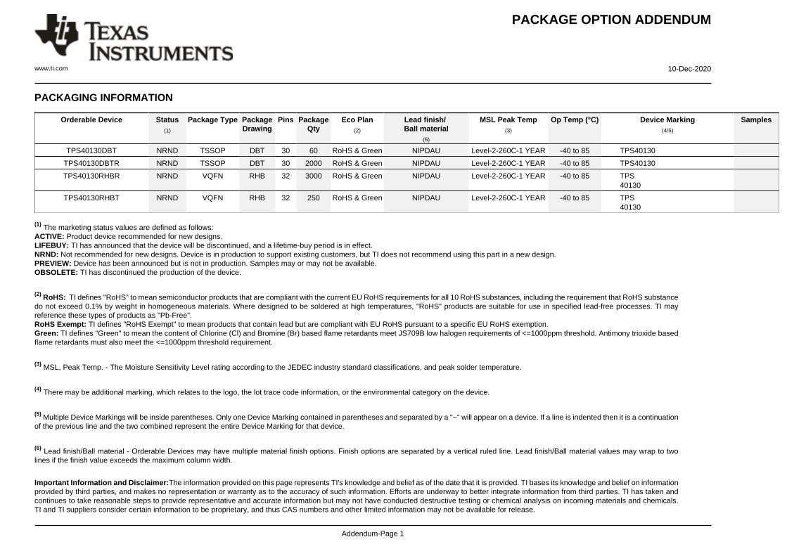
PACKAGING INFORMATION
Orderable Device Status(1)
Package Type PackageDrawing
Pins PackageQty
Eco Plan(2)
Lead finish/Ball material
(6)
MSL Peak Temp(3)
Op Temp (°C) Device Marking(4/5)
Samples
TPS40130DBT NRND TSSOP DBT 30 60 RoHS & Green NIPDAU Level-2-260C-1 YEAR -40 to 85 TPS40130
TPS40130DBTR NRND TSSOP DBT 30 2000 RoHS & Green NIPDAU Level-2-260C-1 YEAR -40 to 85 TPS40130
TPS40130RHBR NRND VQFN RHB 32 3000 RoHS & Green NIPDAU Level-2-260C-1 YEAR -40 to 85 TPS40130
TPS40130RHBT NRND VQFN RHB 32 250 RoHS & Green NIPDAU Level-2-260C-1 YEAR -40 to 85 TPS40130
(1) The marketing status values are defined as follows:ACTIVE: Product device recommended for new designs.LIFEBUY: TI has announced that the device will be discontinued, and a lifetime-buy period is in effect.NRND: Not recommended for new designs. Device is in production to support existing customers, but TI does not recommend using this part in a new design.PREVIEW: Device has been announced but is not in production. Samples may or may not be available.OBSOLETE: TI has discontinued the production of the device.
(2) RoHS: TI defines "RoHS" to mean semiconductor products that are compliant with the current EU RoHS requirements for all 10 RoHS substances, including the requirement that RoHS substancedo not exceed 0.1% by weight in homogeneous materials. Where designed to be soldered at high temperatures, "RoHS" products are suitable for use in specified lead-free processes. TI mayreference these types of products as "Pb-Free".RoHS Exempt: TI defines "RoHS Exempt" to mean products that contain lead but are compliant with EU RoHS pursuant to a specific EU RoHS exemption.Green: TI defines "Green" to mean the content of Chlorine (Cl) and Bromine (Br) based flame retardants meet JS709B low halogen requirements of <=1000ppm threshold. Antimony trioxide basedflame retardants must also meet the <=1000ppm threshold requirement.
(3) MSL, Peak Temp. - The Moisture Sensitivity Level rating according to the JEDEC industry standard classifications, and peak solder temperature.
(4) There may be additional marking, which relates to the logo, the lot trace code information, or the environmental category on the device.
(5) Multiple Device Markings will be inside parentheses. Only one Device Marking contained in parentheses and separated by a "~" will appear on a device. If a line is indented then it is a continuationof the previous line and the two combined represent the entire Device Marking for that device.
(6) Lead finish/Ball material - Orderable Devices may have multiple material finish options. Finish options are separated by a vertical ruled line. Lead finish/Ball material values may wrap to twolines if the finish value exceeds the maximum column width.
Important Information and Disclaimer:The information provided on this page represents TI's knowledge and belief as of the date that it is provided. TI bases its knowledge and belief on informationprovided by third parties, and makes no representation or warranty as to the accuracy of such information. Efforts are underway to better integrate information from third parties. TI has taken andcontinues to take reasonable steps to provide representative and accurate information but may not have conducted destructive testing or chemical analysis on incoming materials and chemicals.TI and TI suppliers consider certain information to be proprietary, and thus CAS numbers and other limited information may not be available for release.
PACKAGE OPTION ADDENDUM
www.ti.com 10-Dec-2020
Addendum-Page 2
In no event shall TI's liability arising out of such information exceed the total purchase price of the TI part(s) at issue in this document sold by TI to Customer on an annual basis.
TAPE AND REEL INFORMATION
*All dimensions are nominal
Device PackageType
PackageDrawing
Pins SPQ ReelDiameter
(mm)
ReelWidth
W1 (mm)
A0(mm)
B0(mm)
K0(mm)
P1(mm)
W(mm)
Pin1Quadrant
TPS40130DBTR TSSOP DBT 30 2000 330.0 16.4 6.95 8.3 1.6 8.0 16.0 Q1
TPS40130RHBR VQFN RHB 32 3000 330.0 12.4 5.3 5.3 1.5 8.0 12.0 Q2
TPS40130RHBT VQFN RHB 32 250 180.0 12.4 5.3 5.3 1.5 8.0 12.0 Q2
PACKAGE MATERIALS INFORMATION
www.ti.com 5-Jan-2022
Pack Materials-Page 1
*All dimensions are nominal
Device Package Type Package Drawing Pins SPQ Length (mm) Width (mm) Height (mm)
TPS40130DBTR TSSOP DBT 30 2000 853.0 449.0 35.0
TPS40130RHBR VQFN RHB 32 3000 853.0 449.0 35.0
TPS40130RHBT VQFN RHB 32 250 210.0 185.0 35.0
PACKAGE MATERIALS INFORMATION
www.ti.com 5-Jan-2022
Pack Materials-Page 2
TUBE
*All dimensions are nominal
Device Package Name Package Type Pins SPQ L (mm) W (mm) T (µm) B (mm)
TPS40130DBT DBT TSSOP 30 60 530 10.2 3600 3.5
PACKAGE MATERIALS INFORMATION
www.ti.com 5-Jan-2022
Pack Materials-Page 3
www.ti.com
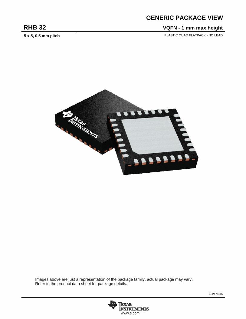
GENERIC PACKAGE VIEW
Images above are just a representation of the package family, actual package may vary.Refer to the product data sheet for package details.
VQFN - 1 mm max heightRHB 32PLASTIC QUAD FLATPACK - NO LEAD5 x 5, 0.5 mm pitch
4224745/A
www.ti.com
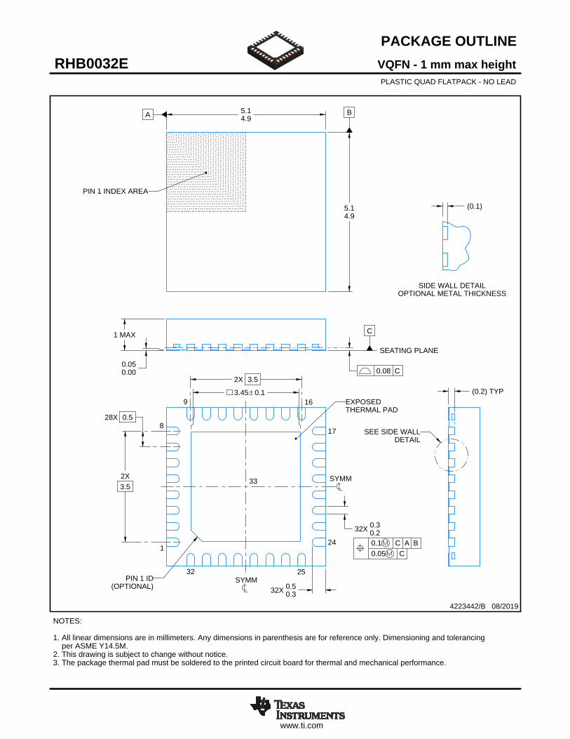
PACKAGE OUTLINE
C
32X 0.30.2
3.45 0.1
32X 0.50.3
1 MAX
(0.2) TYP
0.050.00
28X 0.5
2X3.5
2X 3.5
A 5.14.9
B
5.14.9
(0.1)
VQFN - 1 mm max heightRHB0032EPLASTIC QUAD FLATPACK - NO LEAD
4223442/B 08/2019
PIN 1 INDEX AREA
0.08 C
SEATING PLANE
1
817
24
9 16
32 25
(OPTIONAL)PIN 1 ID
0.1 C A B0.05 C
EXPOSEDTHERMAL PAD
33 SYMM
SYMM
NOTES: 1. All linear dimensions are in millimeters. Any dimensions in parenthesis are for reference only. Dimensioning and tolerancing per ASME Y14.5M. 2. This drawing is subject to change without notice. 3. The package thermal pad must be soldered to the printed circuit board for thermal and mechanical performance.
SCALE 3.000
SEE SIDE WALLDETAIL
20.000
SIDE WALL DETAILOPTIONAL METAL THICKNESS
www.ti.com
EXAMPLE BOARD LAYOUT
(1.475)
0.07 MINALL AROUND
0.07 MAXALL AROUND
32X (0.25)
32X (0.6)
( 0.2) TYPVIA
28X (0.5)
(4.8)
(4.8)
(1.475)
( 3.45)
(R0.05)TYP
VQFN - 1 mm max heightRHB0032EPLASTIC QUAD FLATPACK - NO LEAD
4223442/B 08/2019
SYMM
1
8
9 16
17
24
2532
SYMM
LAND PATTERN EXAMPLESCALE:18X
NOTES: (continued) 4. This package is designed to be soldered to a thermal pad on the board. For more information, see Texas Instruments literature number SLUA271 (www.ti.com/lit/slua271).5. Vias are optional depending on application, refer to device data sheet. If any vias are implemented, refer to their locations shown on this view. It is recommended that vias under paste be filled, plugged or tented.
33
SOLDER MASKOPENING
METAL UNDERSOLDER MASK
SOLDER MASKDEFINED
METAL
SOLDER MASKOPENING
SOLDER MASK DETAILS
NON SOLDER MASKDEFINED
(PREFERRED)
www.ti.com
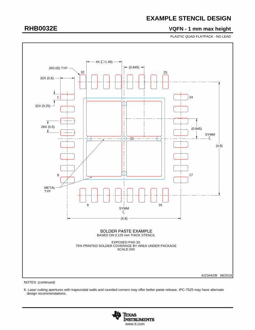
EXAMPLE STENCIL DESIGN
32X (0.6)
32X (0.25)
28X (0.5)
(4.8)
(4.8)
4X ( 1.49)
(0.845)
(0.845)(R0.05) TYP
VQFN - 1 mm max heightRHB0032EPLASTIC QUAD FLATPACK - NO LEAD
4223442/B 08/2019
NOTES: (continued) 6. Laser cutting apertures with trapezoidal walls and rounded corners may offer better paste release. IPC-7525 may have alternate design recommendations.
33
SYMM
METALTYP
SOLDER PASTE EXAMPLEBASED ON 0.125 mm THICK STENCIL
EXPOSED PAD 33:
75% PRINTED SOLDER COVERAGE BY AREA UNDER PACKAGESCALE:20X
SYMM
1
8
9 16
17
24
2532

IMPORTANT NOTICE AND DISCLAIMERTI PROVIDES TECHNICAL AND RELIABILITY DATA (INCLUDING DATA SHEETS), DESIGN RESOURCES (INCLUDING REFERENCE DESIGNS), APPLICATION OR OTHER DESIGN ADVICE, WEB TOOLS, SAFETY INFORMATION, AND OTHER RESOURCES “AS IS” AND WITH ALL FAULTS, AND DISCLAIMS ALL WARRANTIES, EXPRESS AND IMPLIED, INCLUDING WITHOUT LIMITATION ANY IMPLIED WARRANTIES OF MERCHANTABILITY, FITNESS FOR A PARTICULAR PURPOSE OR NON-INFRINGEMENT OF THIRD PARTY INTELLECTUAL PROPERTY RIGHTS.These resources are intended for skilled developers designing with TI products. You are solely responsible for (1) selecting the appropriate TI products for your application, (2) designing, validating and testing your application, and (3) ensuring your application meets applicable standards, and any other safety, security, regulatory or other requirements.These resources are subject to change without notice. TI grants you permission to use these resources only for development of an application that uses the TI products described in the resource. Other reproduction and display of these resources is prohibited. No license is granted to any other TI intellectual property right or to any third party intellectual property right. TI disclaims responsibility for, and you will fully indemnify TI and its representatives against, any claims, damages, costs, losses, and liabilities arising out of your use of these resources.TI’s products are provided subject to TI’s Terms of Sale or other applicable terms available either on ti.com or provided in conjunction with such TI products. TI’s provision of these resources does not expand or otherwise alter TI’s applicable warranties or warranty disclaimers for TI products.TI objects to and rejects any additional or different terms you may have proposed. IMPORTANT NOTICE
Mailing Address: Texas Instruments, Post Office Box 655303, Dallas, Texas 75265Copyright © 2022, Texas Instruments Incorporated