Embed Size (px)
Citation preview

This content has been downloaded from IOPscience. Please scroll down to see the full text.
Download details:
IP Address: 202.118.236.130
This content was downloaded on 08/10/2013 at 23:23
Please note that terms and conditions apply.
Transfer printing of 3D hierarchical gold structures using a sequentially imprinted polymer
stamp
View the table of contents for this issue, or go to the journal homepage for more
2008 Nanotechnology 19 415305
(http://iopscience.iop.org/0957-4484/19/41/415305)
Home Search Collections Journals About Contact us My IOPscience

IOP PUBLISHING NANOTECHNOLOGY
Nanotechnology 19 (2008) 415305 (5pp) doi:10.1088/0957-4484/19/41/415305
Transfer printing of 3D hierarchical goldstructures using a sequentially imprintedpolymer stampFengxiang Zhang and Hong Yee Low1
Institute of Materials Research and Engineering, A*STAR (Agency for Science,Technology and Research), 3 Research Link, 117602, Singapore
E-mail: [email protected]
Received 16 June 2008, in final form 6 August 2008Published 3 September 2008Online at stacks.iop.org/Nano/19/415305
AbstractComplex three-dimensional (3D) hierarchical structures on polymeric materials are fabricatedthrough a process referred to as sequential imprinting. In this work, the sequentially imprintedpolystyrene film is used as a soft stamp to replicate hierarchical structures onto gold (Au) films,and the Au structures are then transferred to a substrate by transfer printing at an elevatedtemperature and pressure. Continuous and isolated 3D structures can be selectively fabricatedwith the assistance of thermo-mechanical deformation of the polymer stamp. HierarchicalAu structures are achieved without the need for a corresponding three-dimensionally patternedmold.
(Some figures in this article are in colour only in the electronic version)
1. Introduction
Characterized by multi-level ordered micro- and nanoscalefeatures, three-dimensional (3D) hierarchical structures havelarge surface area, and provide the possibility of achievingmultiple functionality. Such structures can therefore findinteresting applications in biosensors [1], catalysts [2],photonic devices [3], and as electrodes for fuel cells [4]They are also responsible for the unique properties andfunctionalities in some biological systems, such as the self-cleaning effect of lotus leaves [5], the dry adhesion of agecko’s foot [6], the reduced drag on a shark’s skin [7], andthe exceptional mechanical stability of a Euplectella sponge’sskeleton [8].
In particular, 3D hierarchical metallic structures are ofgreat interest owing to the electrical conductivity, mechanicaland thermal robustness of metals, sensing and catalyticproperties, as in the case of noble metals [9, 10]. Forinstance, an enhancement factor of 104 for surface enhancedRaman spectroscopy was achieved by a hierarchical silver(Ag) substrate [11]; and a 3D structured nickel electroderesulted in improved efficiency of a nickel/metal-hydride
1 Author to whom any correspondence should be addressed.
battery [12]. However, there is limited work reported on thefabrication of 3D hierarchical metallic structures, comparedto the abundant literature for 3D patterning of non-metalssuch as polymers and sol–gel materials through sequentialnanoimprinting [13], self-assembly [14, 15], femtosecond laserlithography [16], capillary force lithography [17], two-photolaser fabrication [18, 19], templating [20–23], and dropletself-organization [24]. In the case of metals, hierarchical Agstructures have been fabricated through immobilization of Agnanoparticles on a pre-patterned substrate [11]. Continuous,3D gold (Au) film has been achieved via nano-transferprinting aided by a slope-walled polydimethylsilane (PDMS)stamp [25]. In the above two examples, the substrates on whichthe Au pattern sits were both modified by thiol molecules,which may impose limitations to the device integrationprocess. In another example, Whang et al achieved hierarchicalpatterning of chromium lines using a hierarchically alignednanowire mask, which was formed by the Langmuir–Blodgettmethod [26]; the resulting array of chromium lines, however,lack ordering and controllability.
In our previous works, we reported a sequentialimprinting technique for fabricating 3D hierarchical polymericstructures [13], and the resulting surface wettability tuningeffects [27, 28]. The technique is capable of creating
0957-4484/08/415305+05$30.00 © 2008 IOP Publishing Ltd Printed in the UK1
Nanotechnology 19 (2008) 415305 F Zhang and H Y Low
large-area, 3D hierarchical structures via combined use of 2Dmolds with varying surface relief patterns. Herein we reportthe application of sequentially imprinted polymeric films asstamps for fabricating 3D hierarchical Au structures that wouldbe impossible or difficult to achieve by other techniques.
2. Experimental details
2.1. Materials
Polystyrene (Mw = 120 000–260 000 g mol−1) waspurchased from Aldrich and used as received without furtherpurification. Silicon molds were fabricated by the Institute ofMicroelectronics Singapore using electron-beam lithography.Two types of mold were used for imprinting: 2 µm (diameter)hemispherical dimple (1:1 duty cycle, 600 nm depth), and250 nm (diameter) flat-bottom dimple (1:1 duty cycle, 250 nmdepth). We define duty cycle as the ratio of the patternwidth/diameter to the spatial distance. The molds were cleanedby ultrasonication in isopropanol (IPA) and oxygen plasmaetching (10 sccm, 250 mT, 100 W RF power, for 10 min), andthen treated with a perfluorodecyltrichlorosilane (FDTS) vaporin an evacuated desiccator for anti-sticking purposes.
2.2. Fabrication of hierarchical polymer stamps
Polystyrene (PS) thin films were prepared by spinning an 8%PS solution (w/v, in toluene) on a well-cleaned Si wafer at1500 revolutions per minute for 30 s, and subsequently bakingat 120 ◦C for 10 min; the resulting films had a thickness ofabout 1.5 µm. To fabricate a hierarchical polymer stamp, aspin-coated PS film was first imprinted with a 2 µm mold(hemispherical dimple or grating) at 140 ◦C, 40 bar for 5 min;upon demolding at 70 ◦C, it was then imprinted with a 250 nmmold (dimple or grating) at 90 ◦C, 40 bar for 10 min. Allthe imprints were made using an Obducat nanoimprinter(Sweden).
2.3. Printing of hierarchical Au structures
Au was deposited on the above prepared hierarchical stampby electron-beam evaporation at an evaporation rate of0.05 nm min−1. The deposited layer was 20–30 nm inthickness. The Au-coated stamp was pressed on a well-cleaned, oxygen-plasma-treated Si substrate at 50 bar, andheated to 110 ◦C for 10 min. After cooling to roomtemperature, the stamp was separated manually from thesubstrate, and the latter was soaked in toluene for 2 min,sonicated in toluene for another 2 min, rinsed with IPA, blowndry with compressed nitrogen, and finally treated with oxygenplasma.
2.4. Characterizations
Scanning electron microscopy (SEM) images were obtained ona JEOL FEG SEM (JSM6700F). PS samples were depositedwith a thin layer of Au (by sputtering) prior to loading into theSEM chamber. No additional Au coating was needed for theAu patterned samples. Tapping mode atomic force microscopy
(AFM) measurements were performed using a MultiModeAFM (Digital Instruments) with a high-aspect-ratio silicon tip(FIB2-100S model). A scanning rate of 0.2 Hz was used.
3. Results and discussion
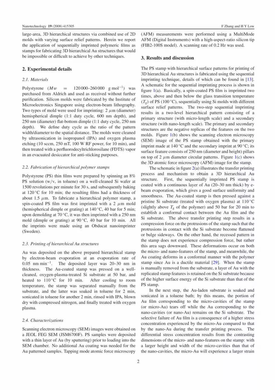
The PS stamp with hierarchical surface patterns for printing of3D hierarchical Au structures is fabricated using the sequentialimprinting technique, details of which can be found in [13].A schematic for the sequential imprinting process is shown infigure 1(a). Basically, a spin-coated PS film is imprinted twotimes, above and then below the glass transition temperature(Tg) of PS (100 ◦C), sequentially using Si molds with differentsurface relief patterns. The two-step sequential imprintingresults in a two-level hierarchical pattern consisting of aprimary structure (with micro-length scale) and a secondarystructure (with nano-length scale). The primary and secondarystructures are the negative replicas of the features on the twomolds. Figure 1(b) shows the scanning electron microscopy(SEM) image of the PS stamp obtained with the primaryimprint made at 140 ◦C and the secondary imprint at 90 ◦C; itssurface feature consists of 250 nm (diameter and height) pillarson top of 2 µm diameter circular patterns. Figure 1(c) showsthe 3D atomic force microscopy (AFM) image for the stamp.
The schematic in figure 2(a) illustrates the transfer printingprocess and mechanism to obtain a 3D hierarchical Austructure. First, the sequentially imprinted PS stamp iscoated with a continuous layer of Au (20–30 nm thick) by e-beam evaporation, which gives a good surface uniformity andsmoothness. The Au-coated stamp is then pressed against apristine Si substrate (treated with oxygen plasma) at 110 ◦C(slightly above Tg of the polymer) and 50 bar for 20 min toestablish a conformal contact between the Au film and theSi substrate. The above transfer printing step results in acompression force on the protrusions of the stamp such that theprotrusions in contact with the Si substrate become flattenedor bulge sideways. On the other hand, the recessed pattern inthe stamp does not experience compression force, but ratherthis area sags downward. These deformations occur on boththe micro- and nano-features of the stamp, and meanwhile, theAu coating deforms in a conformal manner with the polymerstamp since Au is a ductile material [29]. When the stampis manually removed from the substrate, a layer of Au with thereplicated stamp features is retained on the Si substrate becauseof the higher surface energy of the Si substrate than that of thePS stamp.
In the next step, the Au-laden substrate is soaked andsonicated in a toluene bath; by this means, the portion ofAu film corresponding to the micro-cavities of the stamp(or micro-Au) tears off while the Au corresponding to thenano-cavities (or nano-Au) remains on the Si substrate. Theselective failure of Au film is a consequence of a higher stressconcentration experienced by the micro-Au compared to thatby the nano-Au during the transfer printing process. Thedifferential stress concentration results from the contrastingdimensions of the micro- and nano-features on the stamp: witha larger height and width of the micro-cavities than that ofthe nano-cavities, the micro-Au will experience a larger strain
2

Nanotechnology 19 (2008) 415305 F Zhang and H Y Low
Figure 1. (a) Schematic for the sequential imprinting technique; (b) SEM and (c) 3D AFM images for the sequentially imprinted PS stampwith hierarchical surface patterns.
N
Figure 2. (a) Schematic for the printing of 3D hierarchical Au structures using a hierarchical polymer stamp; (b) an expanded schematic forthe different strains of Au occurring in the micro- and nano-cavities of the stamp when pressed at 110 ◦C and 50 bar. The circles in (b)indicate failure of the Au film at corners of the micro-cavities due to a larger stress concentration there than at the corners of nano-cavities.
and thus larger stress than the nano-Au during the thermalpressing of the polymer stamp (figure 2(b)). Corners ofpatterns are where stress concentrates; as a result, the Au filmtears off at the corners of the micro-Au pattern upon sonication.We are currently performing simulation work on the above-described mechanism and the results will be reported in ournext communication.
The Au structures printed from the above process are thenegative replicas of the patterns on the hierarchical polymer
stamp. Figure 3 shows a series of SEM images for theAu printing results. Immediately following stamp/substrateseparation and before sonication of the substrate in toluene,a continuous layer of Au with printed hierarchical structuresis obtained; the hierarchical structures feature a waffle-likestructural format, and consist of an ordered array of submicro-sized, round dimples embedded on a micro-sized circularpattern (figures 3(a) and (b)). Upon sonication in toluene,the Au layer is fractured along the edge of the micro-pattern,
3

Nanotechnology 19 (2008) 415305 F Zhang and H Y Low
Figure 3. SEM images of the 3D hierarchical Au structure (a) whole-layer Au transfer onto the Si substrate with a negative replica of thestamp feature, and (b) a magnified view of the replicated Au structure in image (a), showing submicro-dimples on a micro-pattern,immediately after stamp/substrate separation; (c) isolated Au structures after sonication in toluene, and (d) a magnified view of an isolatedhierarchical structure corresponding to the image in (c); (e) image showing the distinctive region with continuous Au structure and isolated Austructures; (f) image clearly showing the tear line at the micro-pattern.
and the Au between the micro-patterns tears off as analyzedin the preceding section, resulting in the formation of isolatedhierarchical Au structures (figures 3(c) and (d)). There areseveral direct evidences for the above fracturing and tearing-off events: one is the sharp, rough and rolled-up edge of theAu structure after fracturing (figure 3(d)), while the continuousAu film (before sonicating) bears a smooth edge (figure 3(b));the SEM image in figure 3(e) shows a clear contrast of thecontinuous Au pattern and the isolated Au pattern. Figure 3(f)provides another clear SEM image for the tearing of the Aufilm along the edges of the micro-patterns.
The dimensions of the Au structures were measured byAFM line scan profile (figure 4(a)). The submicro-dimplesin the structure have a depth of 31 nm, and their diameter is328 nm, the latter being much larger than that of the nano-pillars on the stamp (250 nm). The wall thickness of thedimples is 156 nm, significantly smaller than the spacingbetween the pillars (also 250 nm) on the stamp. The enlargeddiameter and reduced wall thickness of the submicro-dimplescompared with the stamp geometries are a consequence of the
deformations of the polymer stamp during printing of the Austructure. When compared with the stamp before printing, thestamp after the Au film printing (figure 4(b)) shows broadenedpillar/protrusion and reduced spacing between the pillars, againas a result of the compressive force in the PS stamp during Aufilm printing.
Our strategy for Au transfer printing is different fromconventional micro-contact printing (µCP) or nano-transferprinting (nTP) techniques. In µCP and nTP, a single-levelpatterned PDMS stamp is typically used and the pattern createdis a 2D one [30, 31]. In addition, we can selectively fabricatecontinuous or isolated structures with the assistance of thedeformations of the polymer stamp and by using sonication.It is also worth noting that there is no polymer interfacial layerbetween the printed Au structure and the underlying substrate,since the Au structure remains attached to the substrate anddoes not lift off after the toluene soak. This feature constitutesan important contrast with the work of Helt et al [32], whoused a micro-patterned thermoplastic stamp coated with Auto produce insulated Au nanowires. In their work, Au was
4

Nanotechnology 19 (2008) 415305 F Zhang and H Y Low
Figure 4. (a) AFM line scan for the 3D hierarchical Au structure printed using the circular PS stamp shown in figure 1(d). (b) SEM image ofthe PS stamp after being used for Au printing (scale bar: 200 nm).
deposited only on the horizontal surfaces (both protruding andrecessed), so the Au layer is not continuous, and thus polymerwill seep between the Au and substrate when the stamp ispressed against the substrate at elevated temperatures.
4. Conclusions
In summary, we have demonstrated the fabrication of 3Dhierarchical structures on Au film, which are difficult tofabricate using conventional lithography or other tools. The Austructures, featuring submicro-dimples embedded on circularmicro-patterns, were printed on a Si substrate under elevatedtemperature and pressure using a sequentially imprinted PSfilm as a stamp. Differential thermoplastic deformations andstresses occurring on the micro- and nano-features of the stampwhen pressed against the Si substrate facilitated the formationof isolated, hierarchical Au structures. The method hereinopens up a possibility for making 3D hierarchical Au structureswith various pattern formats, and will benefit the researchand application fields such as microelectronics, lab-on-chips,sensing, and catalysis. The method may also be extendedto hierarchical patterning of other ductile metals. Finally,although we have shown sub-micrometer scale Au patterns,the pattern resolution of the technique described in this reportwill be governed by the mold/template resolution, an intrinsicfeature of nanoimprint lithography (NIL).
Acknowledgments
The authors are grateful to Ms Teo Siew Lang for her assistancein the electron-beam evaporation of Au.
References
[1] Wang C and Zhang Y 2005 Adv. Mater. 17 150[2] Boker A et al 2004 Nat. Mater. 3 302[3] Lee S K, Yi G R, Moon J H, Yang S M and Pine D J 2006
Adv. Mater. 18 2111[4] Zhang Y, Zha S and Liu M 2005 Adv. Mater. 17 487[5] Barthlott W and Neinhuis C 1997 Planta 202 1
[6] Autumn K, Liang L A, Hsieh S T, Zesch W, Kenny T W,Fearing R and Full R J 2000 Nature 405 681
[7] Ball P 1999 Nature 400 507[8] Aizenberg J, Weaver J C, Thanawala M S, Sundar V C,
Morse D E and Fatzl P 2005 Science 309 275[9] He X and Antonelli D 2001 Angew. Chem. Int. Edn 41 214
[10] Tierney M J and Kim H O L 1993 Anal. Chem. 65 3435[11] Song W, Li W, Cheng Y, Jia H, Zhao G, Zhou Y, Yang B,
Xu W, Tian W and Zhao B 2006 J. Raman Spectrosc.37 755
[12] Yao M, Okuno K, Iwaki T, Kato M, Harada K, Park J J,Tanase S and Sakai T 2007 Electrochem. Solid State Lett.10 A56
[13] Zhang F and Low H Y 2006 Nanotechnology 17 1884[14] Black C T 2007 ACS Nano 1 147[15] Li H W and Huck W T S 2004 Nano Lett. 4 1633[16] Passinger S, Saifullah M S M, Reinhardt C,
Subramanian K R V, Chichkov B N and Welland M E 2007Adv. Mater. 19 1218
[17] Suh K Y and Lee H H 2002 Adv. Funct. Mater. 12 405[18] Sun H B and Kawata S 2004 Adv. Polym. Sci. 170 169[19] Yang D, Jhaveri S J and Ober C K 2005 MRS Bull. 30 976[20] Graugnard E, King J S, Gaillot D P and Summers C J 2006
Adv. Funct. Mater. 16 1187[21] Tetreault N, von Freymann G, Deubel M, Hermatschweiler M,
Perez-Willard F, John S, Wegener M and Ozin G A 2006Adv. Mater. 18 457
[22] King J S, Graugnard E and Summers C J 2005 Adv. Mater.17 1010
[23] Yang P, Deng T, Zhao D, Feng P, Pine D, Chmelka B F,Whitesides G M and Stucky G D 1998 Science 282 2244
[24] Park J S, Lee S H, Han T H and Kim S O 2007 Adv. Funct.Mater. 17 2315
[25] Zaumseil J, Meitl M A, Hsu J W P, Acharya B R,Baldwin K W, Loo Y L and Rogers J A 2003Nano Lett. 3 1223
[26] Whang D, Jin S and Lieber C M 2003 Nano Lett. 3 951[27] Zhang F and Low H Y 2007 Langmuir 23 7793[28] Zhang F, Chan J and Low H Y 2008 Appl. Surf. Sci. 254 2975[29] Lee H M, Ge M, Sahu B R, Tarakeshwar P and Kim K S 2003
J. Phys. Chem. B 10 9994[30] Schmid H, Wolf H, Allenspach R, Riel H, Karg S,
Michel B and Delamarche E 2003 Adv. Funct. Mater. 13 145[31] Loo Y L, Hsu J W P, Willett R L, Baldwin K W, West K W and
Rogers J A 2002 J. Vac. Sci. Technol. B 20 2583[32] Helt J M, Drain C M and Bazzan G 2006 J. Am. Chem. Soc.
128 9371
5