Embed Size (px)
Citation preview
TRANSFORMATIVE MANUFACTURING OF 2D MATERIAL FOR THZ RESONATOR
Thesis
Submitted to
The School of Engineering of the
UNIVERSITY OF DAYTON
In Partial Fulfillment of the Requirements for
The Degree of
Master of Science in Electro-Optics
By
Yihan Liu, M.S.
Dayton, Ohio
August 2020
ii
TRANSFORMATIVE MANUFACTURING OF 2D MATERIAL FOR THZ RESONATOR
Name: Liu, Yihan
APPROVED BY:
Jay Mathews, Ph.D. Christopher Muratore, Ph.D.
Advisory Committee Chairman Committee Member
Assistant Professor, Associate Professor,
Physics Chemical and Materials Engineering
Partha Banerjee, Ph.D. Thomas A. Searles, Ph.D.
Committee Member Committee Member
Professor, Associate Professor,
Electro-Optics Physics and Astronomy Department
Robert J. Wilkens, Ph.D., P.E. Eddy M. Rojas, Ph.D., M.A., P.E.
Associate Dean for Research and Innovation Dean, School of Engineering
Professor
School of Engineering
iii
ABSTRACT
TRANSFORMATIVE MANUFACTURING OF 2D MATERIAL FOR THZ RESONATOR
Name: Liu, Yihan
University of Dayton
Advisor: Dr. Jay Mathews
Two-dimensional (2D) materials are ultra-thin (<5 atoms thick) layers that are currently
the subjects of many research studies and publications due to their unique chemical and physical
properties. Molybdenum disulfide (MoS2), like other transition metal dichalcogenides (TMDs),
have different electronic and optical properties compared to bulk materials with the same
composition. These new properties, which include mechanical flexibility and enhanced responses
to incident radiation over a broad spectral range arising from reduced dimensionality are the focus
of our work.
In this proposal, we utilize a new method to rapidly fabricate terahertz (THz) sensors
using 2D MoO2. By using a laser annealing system with an automated, programmable stage to
directly write patterns of material with the desired electronic properties, THz sensors with
different patterns can be easily fabricated in the flexible and low-cost precursor material. This
approach provides an inexpensive and rapid approach for fabrication of THz sensors with no
masking or photolithography steps and allows our team to correlate experimental measurements
of sensor performance to computational simulation results to better understand fundamental
theory of THz sensing mechanisms.

iv
Dedicated to my parents

v
ACKNOWLEDGMENTS
My special thanks are in order to Dr. Jay Mathews, my advisor, for providing the time and
equipment necessary for the work contained herein, and for directing this thesis and bringing it to
its conclusion with patience and expertise.
I would also like to express my appreciation to everyone who has helping me with this work. This
includes Joshua A. Burrow, who offered guidance with the THz spectroscopy measurements;
David Lombardo, who gave advice in the LabView coding with the motion stage; Gary Sevison,
for providing the equipment.; Nick Glavin, Drake Austin and Anna Benton who aided in material
development; Adam Miesle and Hannah Kempel, for assisting me with the fabrication process. I
also deeply appreciate the help given by Dr. Christopher Muratore, who aided all the time
through the project, provide the lab space and equipment, aid in the material development and has
taken time to review the text.
vi
TABLE OF CONTENTS
ABSTRACT……………………………………………………………………………………iii
DEDICATION……………………………………………………………………………........iv
ACKNOWLEDGMENTS………………………………………………………………….......v
LIST OF FIGURES………..…………………………………………………………………..viii
LIST OF TABLES..……………………………………………………………………….........x
LIST OF SYMBOLS/ABBREVIATIONS……………………………………………………..xi
CHAPTER I INTRODUCTION………………………………………………………..…...1
1.1 Organization of the thesis………..………………………………………………..…..1
1.2 Introduction ………………....…………………………………………..………..…...2
CHAPTER II BACKGROUND AND MOTIVATION..…………………….…………...….4
2.1 Metamaterials ………...……..…………………………………………….….……..4
2.2 Terahertz radiation……………..………………………………………..……………6
2.3 Brief history of related work …………………………………………………………8
2.3.1 Brief history of THz metasurfaces …………………………………………….8
2.3.2 Brief history of flexible electronics using MoS2………………………....…...12
CHAPTER III METHODOLOGY…………...……………………………………..………..16
3.1 Method ……………..………………………………………..……………….……...16
3.1.1 Sputtered material precursor ……………………………………………..…..17
3.1.2 Fabrication system ……………………………………………………...……17
3.1.3 Continuous Wave Spectroscopy …………………………………….………..22
3.1.4 Data Analysis ………………………………………………………….……..25
3.1.5 Finite element method simulations ………………………….……….………28
3.2 Materials ……………..………………………………………..………….…...……..31
3.2.1 Substrate investigation …………..…………………………………….....…..31
3.2.2 Raman characterization ………………...……………………………………33

vii
CHAPTER IV DEVICE CHARACTERIZATION ………………….……………….…..38
4.1 4-gap SSRR simulation ……………………………………………………..…………...38
4.2 4-gap SSRR fabrication ………………………………………………………………....40
CHAPTER V SUMMARY AND CONCLUSIONS………………….…………….…...…..41
5.1 Conclusion ……………………………………………………………………….……....41
5.2 Future work ………………………………………………………………………….…..41
BIBLIOGRAPHY ……………………………………………………………………...…...…42
viii
LIST OF FIGURES
Figure 1:Visualization of a conventional material vs a metamaterial [7] ........................................ 4
Figure 2: Ray pass through the boundary between media.1-incident ray; 2-reflected ray; 3-
reflected ray if the second medium is left-handed; 4- reflected ray if the second medium
is right-handed. ................................................................................................................... 6
Figure 3: Electromagnetic spectrum ................................................................................................ 7
Figure 4:Transmittance spectra of previously investigated dielectric materials ............................ 11
Figure 5: (a) CSRR with different lattice periods of 300um, 350um and 400um(b)resonant
frequency as a function of lattice constant (c) resonant frequency as a function of angle
between vertically polarized incident THz wave and the planar MM. (d) transmission
spectrum with increasing asymmetry,0˚,45˚,and 90˚.[28] ................................................. 12
Figure 6: (a) Schematic of the laser annealing process. (b) Raman spectra of the MoS2 with and
without laser annealing. (c) I-V curve from a region before/after laser annealing. [19] .. 13
Figure 7: General work flow .......................................................................................................... 16
Figure 8: Schematic of the laser annealing system. LP, linear polarizer; LCR, liquid crystal
rotator; M1, mirror; BS1, 90:10 beam splitter;BS2, 50:50 beam splitter; PM, power
meter; DC, digital camera L1, microscope objective lens. .............................................. 18
Figure 9: Standard liquid crystal variable attenuator design using crossed linear polarizers. ....... 19
Figure 10: The power of power diode and power meter at different LCR voltage ........................ 20
Figure 11: Schematic of how the laser patterning system operation. (a) A sample image of a
pattern; (b) The pixel map transfer from the photo in (a); (c) The shutter blocks the laser
light when it reads a white pixel; (d) The shutter allows the laser light to pass. .............. 21
Figure 12: Schematic of the fiber coupled CW THz spectrometer. ............................................... 24
Figure 13: The schematic of the THz CW spectroscopy ............................................................... 25
Figure 14: THz Power spectrum of air in the test area with water features labeled ...................... 26
ix
Figure 15: : transmission spectra of different meta-atom lattice 4-gap CSRR .............................. 27
Figure 16: (a) simulation example of one 4-gap circle split ring resonator, (b) optical photo of
CSRR with 300um; (c) optical photo of CSRR with 325um; (d) optical photo of CSRR
with 350 um. The “a” represent the lattice constant between each atom. ......................... 30
Figure 17: Measured and simulation data for lattice constant of (a) 300um (b) 325um and (c)
350um, and the combination of different simulation results of different lattice constant
CSRR. ............................................................................................................................... 30
Figure 18: Transmission spectra of (a) 500 µm, (b) 100 µm thick willow glass. .......................... 32
Figure 19: transmission curve for three different substrates .......................................................... 33
Figure 20: Fabricated line precursor sample .................................................................................. 34
Figure 21: Raman spectrum under different condition .................................................................. 35
Figure 22: Raman spectra at different condition(a) at 100mW and 10000µm/s (b)reference
Raman spectra for different material [45] (c) at 150mW and 3000µm/s (d) at 200mW
and 3000µm/s .................................................................................................................... 36
Figure 23: (a) Example of module of a 4-gap SSRR MMs atom,(b) transmission curves with
different value of electron conductivities σ, (c)transmission curve with different value
of thermal conductivities κ. .............................................................................................. 38
Figure 24: The simulation result of the MoO2 annealing resonator with different electric
conductivity ...................................................................................................................... 39

x
LIST OF TABLES
Table 1: Selected symmetric geometries examples…………………………...……………….....10
Table 2: Selected asymmetric geometries examples…………………………………...……… 10
xi
LIST OF ABBREVIATIONS AND NOTATIONS
TMDs Transition Metal Dichalcogenides
NEMS Nanoelectromechanical System
MoS2 Molybdenum Disulfide
LP Linear Polarizer
LCR Liquid crystal retarder
M1 Mirror 1
BS Beam splitter
DC Digital Camera
PD Photodiode
LED Light-emitting diode
DAQ Data Acquisition
1
CHAPTER I
INTRODUCTION
1.1 Organization of the thesis
The thesis starts with introduction of the research in Chapter 1, and the basic principles
about the THz sensors and 2D material are presented. Furthermore, a new way to rapidly
fabricate terahertz sensors using 2D MoS2 is described here.
In Chapter 2, the theoretical background of the thesis is introduced, including the terahertz
radiation, metasurfaces, the brief history of THz sensing and the utilization of flexible electronics
especially using MoS2. And the motivation we start this project is followed.
In Chapter 3, the detailed methodology is discussed. First, the method is presented, including
the working principles of the types of spectroscopy we are using, the detailed design, operation,
and components of the fabrication system, the data analysis techniques we have used to process
the measured data, and the simulation results compared with the actual measurement result. Apart
from this, the materials we used are also discussed here.
Chapter 4 will provide results from several different approaches for material
characterization, starting with lines of transformed material fabricated over a range of selected
incident laser power and laser scan rates over the sample surface. The material structure and
defect densities were characterized via Raman spectroscopy, and the conditions yielding the
phase with the desired properties to fabricate electrically conductive MoO2 and semiconducting
MoS2 were be determined. Once processing conditions of materials with useful properties for
device fabrication are established, a prototype device is presented and tested by CW spectra for
the Thz transmission property.
Followed are the summary, conclusion and future work in chapter 5.
2
1.2 Introduction
Sensing of biological and chemical materials is necessary for a number of applications that
are important for both the military and society at large[1,2]. Chemical and biological sensing can
be used to identify explosives or biological agents for national security purposes, to help detect
chemical or gas leaks, or to monitor protein levels in blood for human performance[3]. With this
proposed work, we seek to create a new path to inexpensive, flexible sensors for such
applications.
THz radiation consists of electromagnetic waves with frequencies in the THz range, in
between infrared and microwaves. Such radiation can be useful for detection of chemical and
biological materials[4,5], for 3D imaging of visually opaque structures, and even for
electromagnetic cloaking[3]. However, due to the low interaction between THz radiation and
matter, high-sensitivity sensors require the use of resonators.
Metamaterials, as artificially designed materials, have the periodic structures that produce
electromagnetic resonances and by changing the size, density, shape and orientation, the specific
electromagnetic response can be tuned [6], thus MMs have been used to create resonators with
frequencies in the THz range. Two-dimensional metamaterials, typically referred to metasurfaces
composed of metallic resonators deposited in a periodic array on a dielectric substrate, have
shown highly sensitive chemical or biological detection and their dimension since the dimension
is small and has a tunable resonant frequency by design, However, the fabrication process need
involve cleanroom environment which is relatively costly and with complex equipment requiring
specialized training for its operation.
Molybdenum disulfide (MoS2), as one of the transition metal dichalcogenides (TMDs) has
emerged as a new 2D material beyond graphene for use in nanoelectromechanical system
(NEMS), and is of great interest for fundamental studies of mechanics at nanoscale[7].
Monolayer MoS2 has desirable properties like relatively high charge mobility, a direct bandgap
of 1.8eV[8], great transparency and high flexibility[7][9]. All these properties make MoS2 an
3
ideal choice for use of NEMS. The TMD materials, when deposited, are typically amorphous
materials with insulating properties. However, by illuminating the material with a laser, it is
possible to crystallize and oxidize the material(MoO2), which can alter the properties to be
semiconducting or metallic. This is achieved by the laser system and moving the amorphous
MoS2 sample at different speeds for micro-size control of crystallization and reaction.
In this thesis, I explore a new way to fabricate THz sensors using 2D materials. In contrast to
the typical thin-film planar metamaterial(MM)-based sensor device, this sensor will be fabricated
using an amorphous precursor material which is one of the transition metal
dichalcogenides(TMDs), MoS2. The material is transformed into different phases with our laser-
annealing method instead of using metals deposited in the traditional way, which brings benefits
to both the fabrication process and the cost. Since sensing of biological and chemical materials is
necessary for applications in both the military and society, such as detecting chemical or gas leak,
or to monitor protein levels in blood for human performance [1], we seek to create a new path to
inexpensive, flexible sensors for such applications.
To pattern these materials outside of the cleanroom environment, the alternative strategy has
been provided here, which has enabled rapid prototyping and eliminated design constraints
imposed by traditional fabrication. This approach using laser processing is utilized to directly
realize several results within an amorphous molybdenum disulfide thin film precursor, such as
conducting, insulating and semiconducting phases. Instead of additive nor subtractive, this is a
transformative manufacturing strategy.
4
CHAPTER II
BACKGROUND AND MOTIVATION
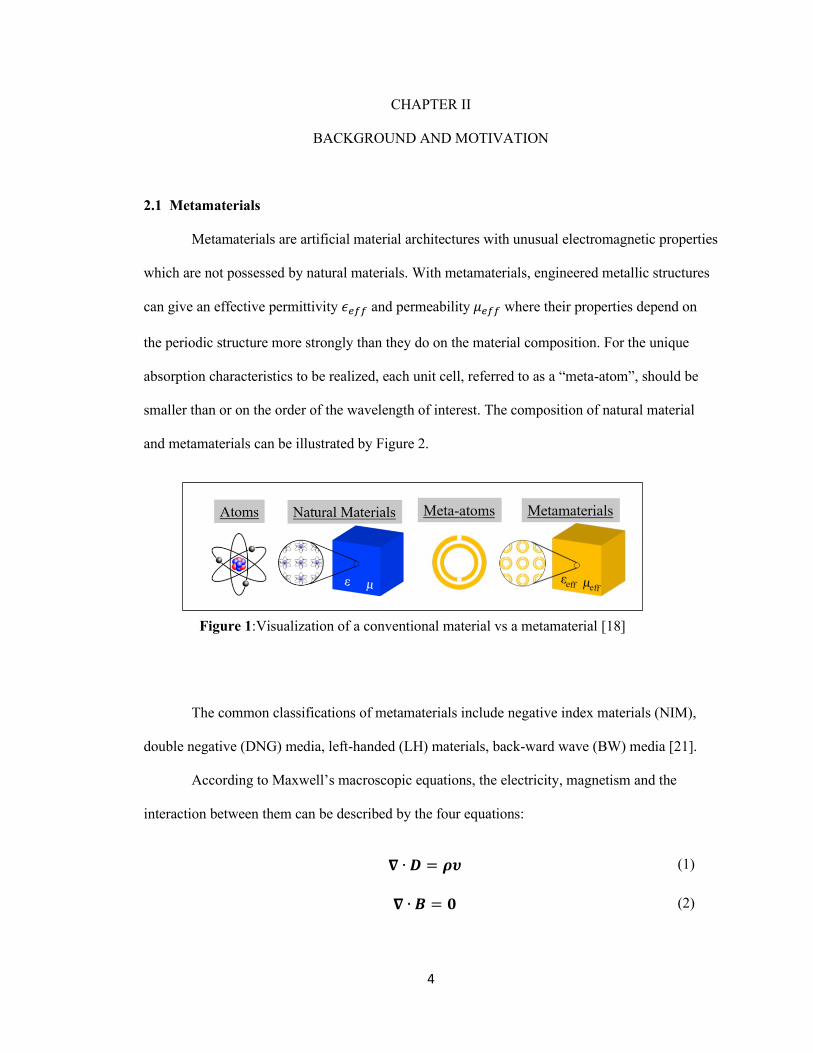
2.1 Metamaterials
Metamaterials are artificial material architectures with unusual electromagnetic properties
which are not possessed by natural materials. With metamaterials, engineered metallic structures
can give an effective permittivity 𝜖𝑒𝑓𝑓 and permeability 𝜇𝑒𝑓𝑓 where their properties depend on
the periodic structure more strongly than they do on the material composition. For the unique
absorption characteristics to be realized, each unit cell, referred to as a “meta-atom”, should be
smaller than or on the order of the wavelength of interest. The composition of natural material
and metamaterials can be illustrated by Figure 2.
The common classifications of metamaterials include negative index materials (NIM),
double negative (DNG) media, left-handed (LH) materials, back-ward wave (BW) media [21].
According to Maxwell’s macroscopic equations, the electricity, magnetism and the
interaction between them can be described by the four equations:
𝛁 ∙ 𝑫 = 𝝆𝝊 (1)
𝛁 ∙ 𝑩 = 𝟎
(2)
Figure 1:Visualization of a conventional material vs a metamaterial [18]
5
𝛁 × 𝑬 = −
𝝏𝑩
𝝏𝒕
(3)
𝛁 × 𝑯 = 𝑱 +
𝝏𝑫
𝝏𝒕
(4)
Where E is the electric field intensity, D is the electric flux density, B is the magnetic
flux density, and H is the magnetic field intensity. At sufficiently low intensities, the electric
current density J is connected to E through Ohm’s law:
𝑱 = 𝜎𝑬
(5)
Where σ is the electrical conductivity. In addition, there’s constitutive relations
specifying the response between displacement field D and the electric field E, as well as the
magnetizing field H and the magnetic field B.
𝑫 = 𝜖𝑬 = 𝜖0(𝑬 + 𝑷) (6)
𝑩 = 𝜇𝑯 = 𝜇0(𝑯 + 𝑴) (7)
Where P is the electric polarization and M is the magnetization density. The 𝜖 and 𝜇 are
permittivity and permeability respectively, which are in dependent on the medium, i.e. 𝜖 ≡ 𝜖(𝒓)
and 𝜇 ≡ 𝜇(𝒓). In a metamaterial, both the electrical permittivity and the magnetic permeability
are negative[6], the refractive index of metamaterials n is also negative:
𝑛 = −√𝜖𝜇 (8)
6
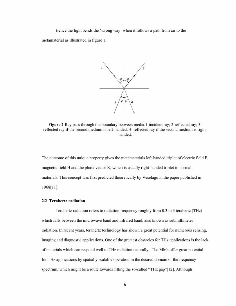
Hence the light bends the ‘wrong way’ when it follows a path from air to the
metamaterial as illustrated in figure 1.
Figure 2:Ray pass through the boundary between media.1-incident ray; 2-reflected ray; 3-
reflected ray if the second medium is left-handed; 4- reflected ray if the second medium is right-
handed.
The outcome of this unique property gives the metamaterials left-handed triplet of electric field E,
magnetic field H and the phase vector K, which is usually right-handed triplet in normal
materials. This concept was first predicted theoretically by Veselago in the paper published in
1968[11].
2.2 Terahertz radiation
Terahertz radiation refers to radiation frequency roughly from 0.3 to 3 terahertz (THz)
which falls between the microwave band and infrared band, also known as submillimeter
radiation. In recent years, terahertz technology has shown a great potential for numerous sensing,
imaging and diagnostic applications. One of the greatest obstacles for THz applications is the lack
of materials which can respond well to THz radiation naturally. The MMs offer great potential
for THz applications by spatially scalable operation in the desired domain of the frequency
spectrum, which might be a route towards filling the so-called “THz gap”[12]. Although
7
theoretically MM structure can be operated in any domain of the frequency spectrum, it’s still a
challenging to approach high frequencies in the visible region, in terms of the minimal sizes
required to fabricate.
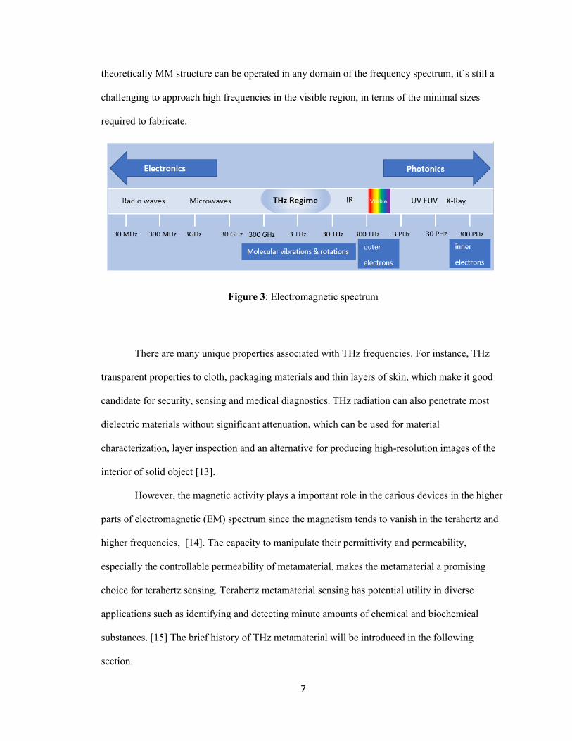
Figure 3: Electromagnetic spectrum
There are many unique properties associated with THz frequencies. For instance, THz
transparent properties to cloth, packaging materials and thin layers of skin, which make it good
candidate for security, sensing and medical diagnostics. THz radiation can also penetrate most
dielectric materials without significant attenuation, which can be used for material
characterization, layer inspection and an alternative for producing high-resolution images of the
interior of solid object [13].
However, the magnetic activity plays a important role in the carious devices in the higher
parts of electromagnetic (EM) spectrum since the magnetism tends to vanish in the terahertz and
higher frequencies, [14]. The capacity to manipulate their permittivity and permeability,
especially the controllable permeability of metamaterial, makes the metamaterial a promising
choice for terahertz sensing. Terahertz metamaterial sensing has potential utility in diverse
applications such as identifying and detecting minute amounts of chemical and biochemical
substances. [15] The brief history of THz metamaterial will be introduced in the following
section.
8
2.3 Brief history of related work
2.3.1 Brief history of THz metasurfaces
Negative index materials (NIMs) possess simultaneously negative electrical permittivity
and magnetic permeability, as shown in the work of Veselago [11]. Later in 1999, the periodic
three-dimensional array of metallic split ring resonators was identified as an approach to achieve
negative permittivity 𝜖 by J.B Pendry et al..[14] Three years later, he further proposed a periodic
array of split ring resonators (SRRs) could have a frequency band where permeability 𝜇 is
negative.
To create a metamaterial which have both negative permittivity and permeability, it is
necessary to combine two elements, which one provides negative 𝜖 and the other provides
negative 𝜇.
In the same year, 2-D array of repeated circle split ring structures in combination with
copper strips demonstrated a negative index of refraction in the microwave regime by D.R. Smith
group’s experiment[16]. After this, many attempts to tune properties by slightly changing the
design of the split ring resonators (SRRs) were investigated and published. Some of these patterns
have led to many unique effects, such as negative refraction [16], super lensing [17], and slow
light effects [18], which attracts attention towards THz and optical applications, including
frequency tunable filters [19].
MM structures have the unique advantage of adjustable electric and magnetic responses
by the geometry of the metallic structures, where the most popular MM structures are the cross
and ring shape structures [14], split-ring resonators (SRRs) [20,21], cut-wires (CWs) or other
complementary structures. These geometries exhibit anisotropic properties independent of the
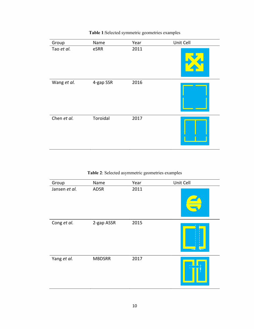
polarization state of the incident coherent radiation, the table 1 have shown some example of the
geometries.
9
The effect of inducing asymmetry into the SRR structure is another direction of MM
design, the asymmetric structural parameter might increase the number of enhanced resonant
frequencies [20-23]. Table 2 shows some asymmetrically unit cell designs.
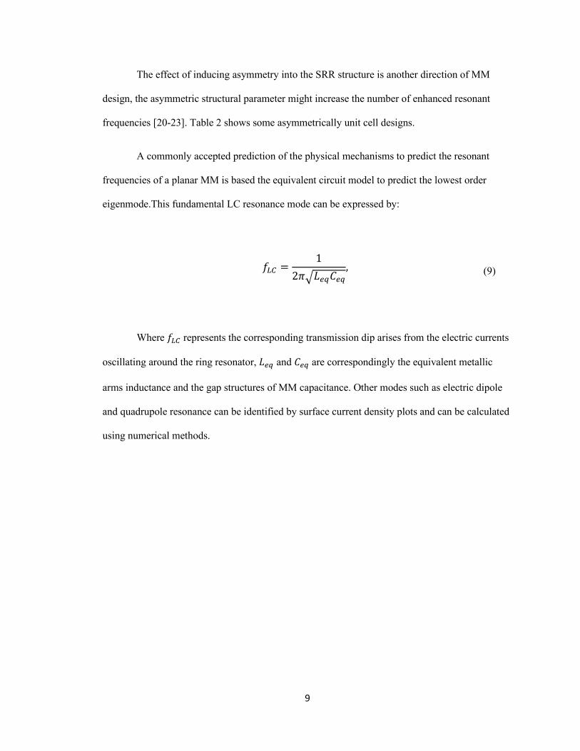
A commonly accepted prediction of the physical mechanisms to predict the resonant
frequencies of a planar MM is based the equivalent circuit model to predict the lowest order
eigenmode.This fundamental LC resonance mode can be expressed by:
𝑓𝐿𝐶 =
1
2𝜋√𝐿𝑒𝑞𝐶𝑒𝑞
,
(9) 0
Where 𝑓𝐿𝐶 represents the corresponding transmission dip arises from the electric currents
oscillating around the ring resonator, 𝐿𝑒𝑞 and 𝐶𝑒𝑞 are correspondingly the equivalent metallic
arms inductance and the gap structures of MM capacitance. Other modes such as electric dipole
and quadrupole resonance can be identified by surface current density plots and can be calculated
using numerical methods.
10
Table 1:Selected symmetric geometries examples
Group Name Year Unit Cell
Tao et al. eSRR 2011
Wang et al. 4-gap SSR 2016
Chen et al. Toroidal 2017
Table 2: Selected asymmetric geometries examples
Group Name Year Unit Cell
Jansen et al. ADSR 2011
Cong et al. 2-gap ASSR 2015
Yang et al. MBDSRR 2017
11
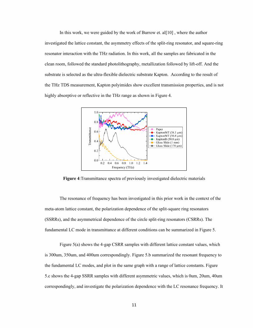
In this work, we were guided by the work of Burrow et. al[10] , where the author
investigated the lattice constant, the asymmetry effects of the split-ring resonator, and square-ring
resonator interaction with the THz radiation. In this work, all the samples are fabricated in the
clean room, followed the standard photolithography, metallization followed by lift-off. And the
substrate is selected as the ultra-flexible dielectric substrate Kapton. According to the result of
the THz TDS measurement, Kapton polyimides show excellent transmission properties, and is not
highly absorptive or reflective in the THz range as shown in Figure 4.
Figure 4:Transmittance spectra of previously investigated dielectric materials
The resonance of frequency has been investigated in this prior work in the context of the
meta-atom lattice constant, the polarization dependence of the split-square ring resonators
(SSRRs), and the asymmetrical dependence of the circle split-ring resonators (CSRRs). The
fundamental LC mode in transmittance at different conditions can be summarized in Figure 5.
Figure 5(a) shows the 4-gap CSRR samples with different lattice constant values, which
is 300um, 350um, and 400um correspondingly. Figure 5.b summarized the resonant frequency to
the fundamental LC modes, and plot in the same graph with a range of lattice constants. Figure
5.c shows the 4-gap SSRR samples with different asymmetric values, which is 0um, 20um, 40um
correspondingly, and investigate the polarization dependence with the LC resonance frequency. It
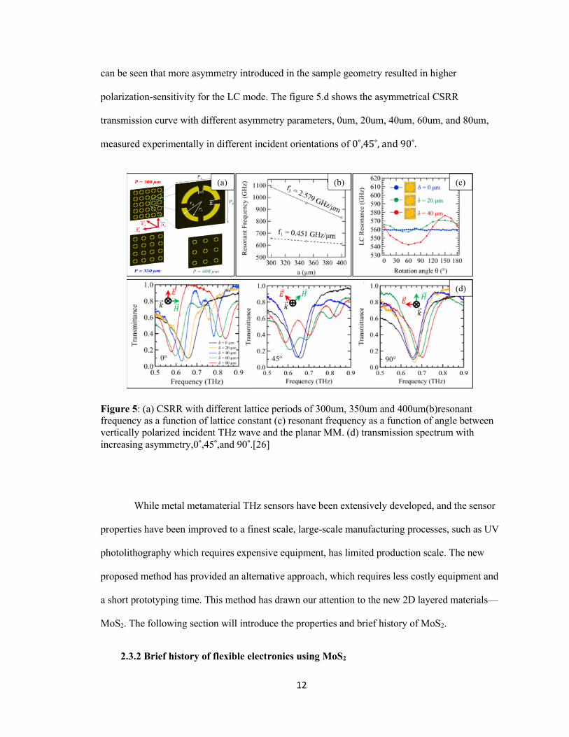
12
can be seen that more asymmetry introduced in the sample geometry resulted in higher
polarization-sensitivity for the LC mode. The figure 5.d shows the asymmetrical CSRR
transmission curve with different asymmetry parameters, 0um, 20um, 40um, 60um, and 80um,
measured experimentally in different incident orientations of 0˚,45˚, and 90˚.
Figure 5: (a) CSRR with different lattice periods of 300um, 350um and 400um(b)resonant
frequency as a function of lattice constant (c) resonant frequency as a function of angle between
vertically polarized incident THz wave and the planar MM. (d) transmission spectrum with
increasing asymmetry,0˚,45˚,and 90˚.[26]
While metal metamaterial THz sensors have been extensively developed, and the sensor
properties have been improved to a finest scale, large-scale manufacturing processes, such as UV
photolithography which requires expensive equipment, has limited production scale. The new
proposed method has provided an alternative approach, which requires less costly equipment and
a short prototyping time. This method has drawn our attention to the new 2D layered materials—
MoS2. The following section will introduce the properties and brief history of MoS2.
2.3.2 Brief history of flexible electronics using MoS2
13
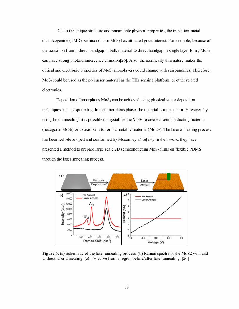
Due to the unique structure and remarkable physical properties, the transition-metal
dichalcogenide (TMD) semiconductor MoS2 has attracted great interest. For example, because of
the transition from indirect bandgap in bulk material to direct bandgap in single layer form, MoS2
can have strong photoluminescence emission[26]. Also, the atomically thin nature makes the
optical and electronic properties of MoS2 monolayers could change with surroundings. Therefore,
MoS2 could be used as the precursor material as the THz sensing platform, or other related
electronics.
Deposition of amorphous MoS2 can be achieved using physical vapor deposition
techniques such as sputtering. In the amorphous phase, the material is an insulator. However, by
using laser annealing, it is possible to crystallize the MoS2 to create a semiconducting material
(hexagonal MoS2) or to oxidize it to form a metallic material (MoO2). The laser annealing process
has been well-developed and conformed by Mcconney et. al[24]. In their work, they have
presented a method to prepare large scale 2D semiconducting MoS2 films on flexible PDMS
through the laser annealing process.
Figure 6: (a) Schematic of the laser annealing process. (b) Raman spectra of the MoS2 with and
without laser annealing. (c) I-V curve from a region before/after laser annealing. [26]
(a)
(b) (c)
14
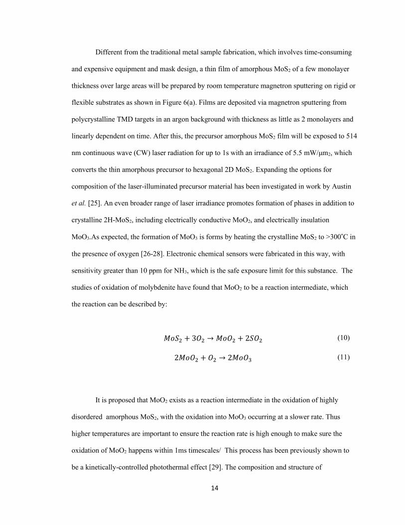
Different from the traditional metal sample fabrication, which involves time-consuming
and expensive equipment and mask design, a thin film of amorphous MoS2 of a few monolayer
thickness over large areas will be prepared by room temperature magnetron sputtering on rigid or
flexible substrates as shown in Figure 6(a). Films are deposited via magnetron sputtering from
polycrystalline TMD targets in an argon background with thickness as little as 2 monolayers and
linearly dependent on time. After this, the precursor amorphous MoS2 film will be exposed to 514
nm continuous wave (CW) laser radiation for up to 1s with an irradiance of 5.5 mW/μm2, which
converts the thin amorphous precursor to hexagonal 2D MoS2. Expanding the options for
composition of the laser-illuminated precursor material has been investigated in work by Austin
et al. [25]. An even broader range of laser irradiance promotes formation of phases in addition to
crystalline 2H-MoS2, including electrically conductive MoO2, and electrically insulation
MoO3.As expected, the formation of MoO3 is forms by heating the crystalline MoS2 to >300˚C in
the presence of oxygen [26-28]. Electronic chemical sensors were fabricated in this way, with
sensitivity greater than 10 ppm for NH3, which is the safe exposure limit for this substance. The
studies of oxidation of molybdenite have found that MoO2 to be a reaction intermediate, which
the reaction can be described by:
𝑀𝑜𝑆2 + 3𝑂2 → 𝑀𝑜𝑂2 + 2𝑆𝑂2 (10)
2𝑀𝑜𝑂2 + 𝑂2 → 2𝑀𝑜𝑂3 (11)
It is proposed that MoO2 exists as a reaction intermediate in the oxidation of highly
disordered amorphous MoS2, with the oxidation into MoO3 occurring at a slower rate. Thus
higher temperatures are important to ensure the reaction rate is high enough to make sure the
oxidation of MoO2 happens within 1ms timescales/ This process has been previously shown to
be a kinetically-controlled photothermal effect [29]. The composition and structure of

15
photonically annealed materials made in this way were evaluated by X-ray photoelectron
spectroscopy and Raman spectra, and the electrical properties are measured by C-AFM (Figure
6(b) and 6(c)) in addition to other approaches. The primary advantage of this approach for
simultaneous materials synthesis and device fabrication is flexibility as alteration of MM
structure only requires re-programming of the laser path on the surface of the material rather than
pattern design and fabrication of masks and photolithography processes to achieve the desired
structure.
16
CHAPTER III
METHODOLOGY
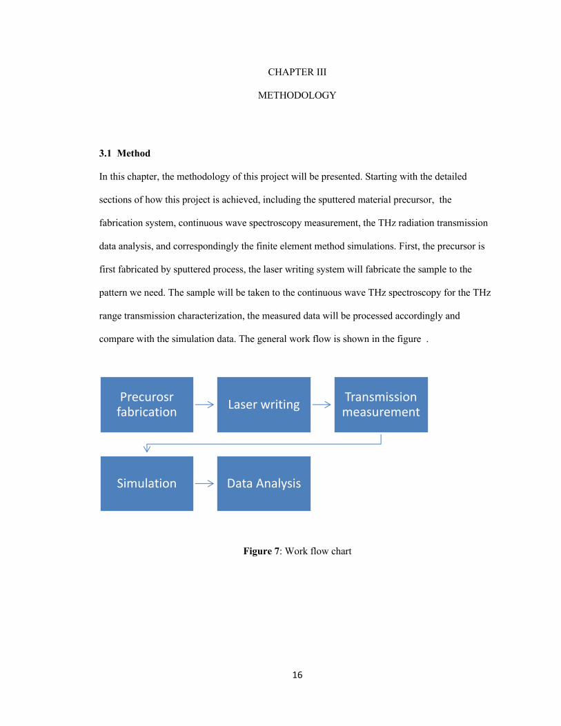
3.1 Method
In this chapter, the methodology of this project will be presented. Starting with the detailed
sections of how this project is achieved, including the sputtered material precursor, the
fabrication system, continuous wave spectroscopy measurement, the THz radiation transmission
data analysis, and correspondingly the finite element method simulations. First, the precursor is
first fabricated by sputtered process, the laser writing system will fabricate the sample to the
pattern we need. The sample will be taken to the continuous wave THz spectroscopy for the THz
range transmission characterization, the measured data will be processed accordingly and
compare with the simulation data. The general work flow is shown in the figure .
Figure 7: Work flow chart
Precurosr fabrication
Laser writingTransmission measurement
Simulation Data Analysis
17
3.1.1 Sputtered Material Precursor
To start our fabrication process, the precursor material amorphous MoS2 in this project is
deposited on a substrate using RF magnetron sputtering. A 900 μm thick film of amorphous MoS2
(a-MoS2) is deposited at a substrate temperature of 25°C. Sputtering was performed via
asymmetric bi-polar pulsed direct current magnetron sputtering at 65 kHz (with a 0.4 µs reverse
time) from a polycrystalline MoS2 target at room temperature with a growth rate of approximately
1 atomic layer per second[25]. This technique can also be used to grow ultra-thin films to produce
thicker films the growth time was extended to 60 min.
The substrate here should be flexible and dielectric material, in this case, two material
will be used in this project: PDMS and willow glass. Detailed properties will be discussed in the
following section.
3.1.2 Fabrication System
In order to fabricate device structures from the deposited materials, I have constructed a
laser annealing system for fabrication. This is an automated, computer-controlled system that can
produce arbitrary laser annealing patterns on a 2D surface. The goal is to anneal the deposited
amorphous MoS2 in areas under various illumination conditions to produce semiconducting and
conducting areas that can be used for electronic and photonic devices.
To achieve our objectives, we have constructed a laser annealing system for sample
fabrication. This is an automated, computer-controlled system that can produce arbitrary laser
annealing patterns on a 2D surface. The goal is to anneal the deposited amorphous MoS2 in areas
under various illumination conditions to produce semiconducting and conducting areas that can
be used for electronic and photonic devices. The overall schematic of annealing system is shown
as Figure 8.
18
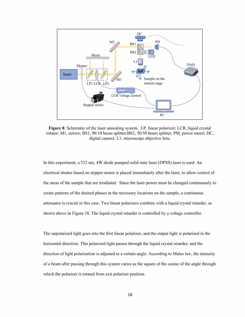
Figure 8: Schematic of the laser annealing system. LP, linear polarizer; LCR, liquid crystal
rotator; M1, mirror; BS1, 90:10 beam splitter;BS2, 50:50 beam splitter; PM, power meter; DC,
digital camera L1, microscope objective lens.
In this experiment, a 532 nm, 4W diode pumped solid state laser (DPSS) laser is used. An
electrical shutter based on stepper motor is placed immediately after the laser, to allow control of
the areas of the sample that are irradiated. Since the laser power must be changed continuously to
create patterns of the desired phases in the necessary locations on the sample, a continuous
attenuator is crucial in this case. Two linear polarizers combine with a liquid crystal retarder, as
shown above in Figure 10. The liquid crystal retarder is controlled by a voltage controller.
The unpolarized light goes into the first linear polarizer, and the output light is polarized in the
horizontal direction. This polarized light passes through the liquid crystal retarder, and the
direction of light polarization is adjusted to a certain angle. According to Malus law, the intensity
of a beam after passing through this system varies as the square of the cosine of the angle through
which the polarizer is rotated from exit polarizer position.
LED
laser
Shutter
LP1 LP2 LCR M1
M2 BS1
PD
L1
Sample on the
motion stage
Block
LCR voltage control
Stepper motor
BS2
DAQ
PC
DC
19
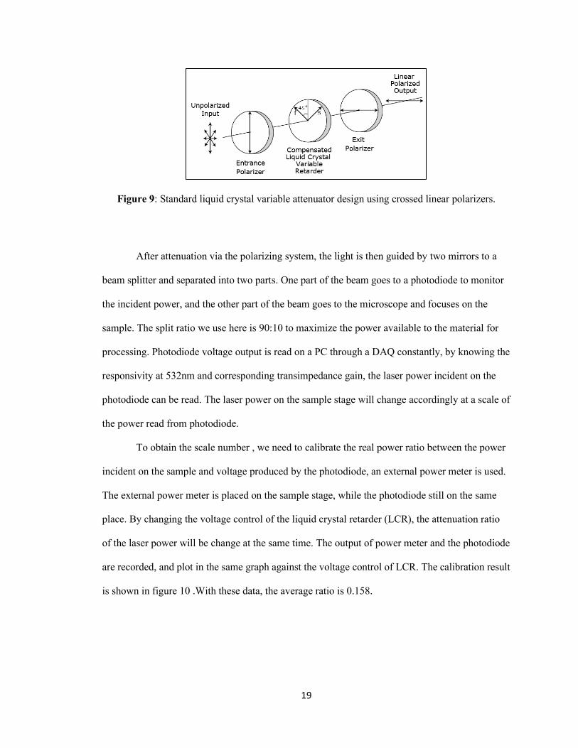
Figure 9: Standard liquid crystal variable attenuator design using crossed linear polarizers.
After attenuation via the polarizing system, the light is then guided by two mirrors to a
beam splitter and separated into two parts. One part of the beam goes to a photodiode to monitor
the incident power, and the other part of the beam goes to the microscope and focuses on the
sample. The split ratio we use here is 90:10 to maximize the power available to the material for
processing. Photodiode voltage output is read on a PC through a DAQ constantly, by knowing the
responsivity at 532nm and corresponding transimpedance gain, the laser power incident on the
photodiode can be read. The laser power on the sample stage will change accordingly at a scale of
the power read from photodiode.
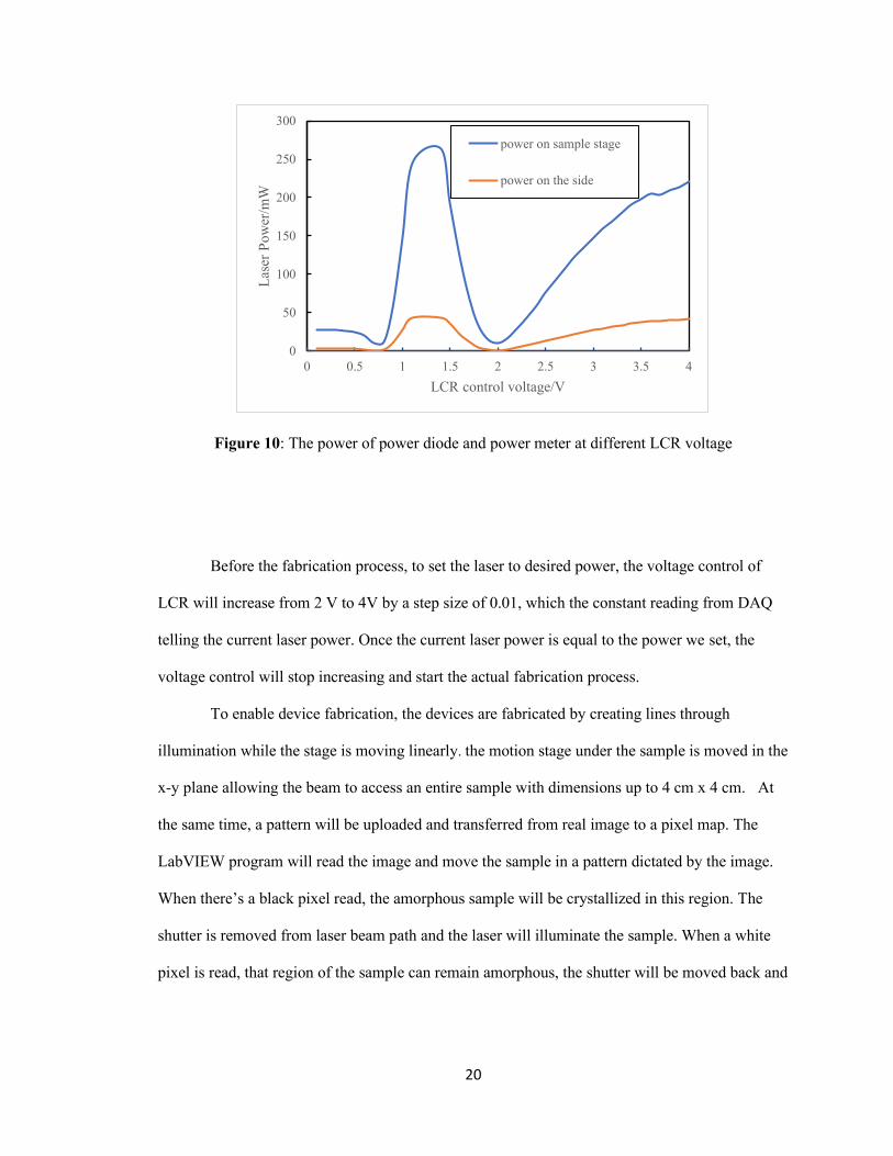
To obtain the scale number , we need to calibrate the real power ratio between the power
incident on the sample and voltage produced by the photodiode, an external power meter is used.
The external power meter is placed on the sample stage, while the photodiode still on the same
place. By changing the voltage control of the liquid crystal retarder (LCR), the attenuation ratio
of the laser power will be change at the same time. The output of power meter and the photodiode
are recorded, and plot in the same graph against the voltage control of LCR. The calibration result
is shown in figure 10 .With these data, the average ratio is 0.158.
20
Figure 10: The power of power diode and power meter at different LCR voltage
Before the fabrication process, to set the laser to desired power, the voltage control of
LCR will increase from 2 V to 4V by a step size of 0.01, which the constant reading from DAQ
telling the current laser power. Once the current laser power is equal to the power we set, the
voltage control will stop increasing and start the actual fabrication process.
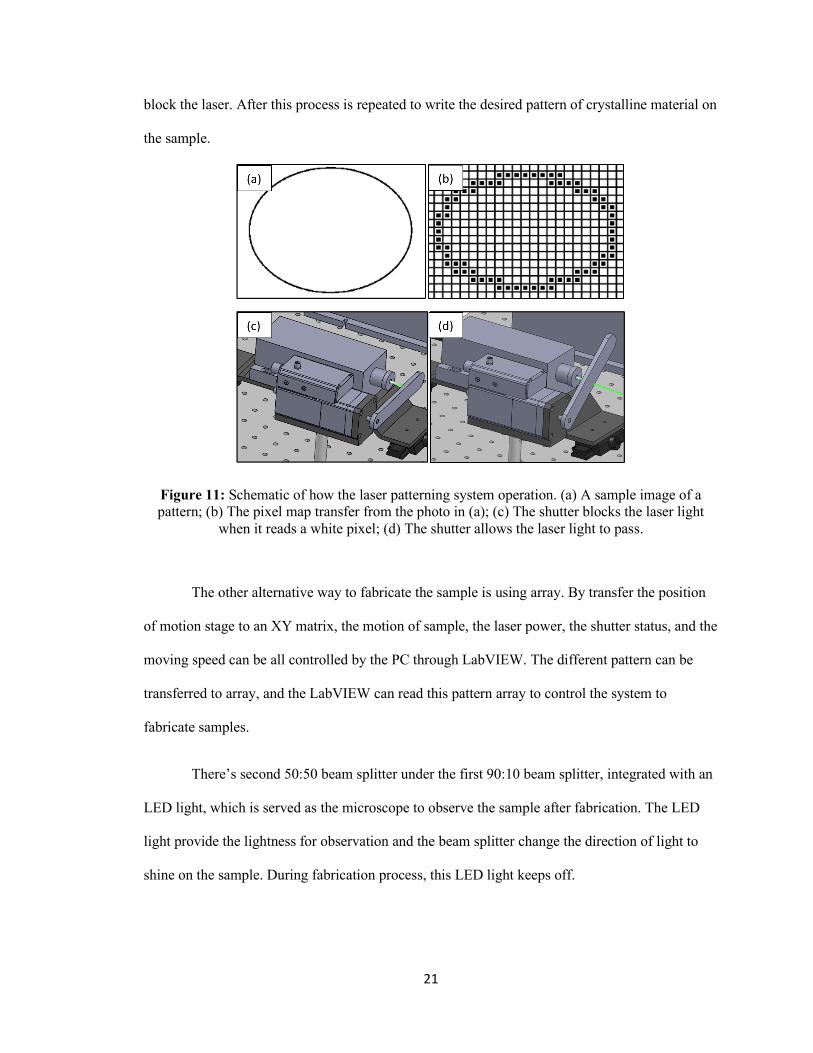
To enable device fabrication, the devices are fabricated by creating lines through
illumination while the stage is moving linearly. the motion stage under the sample is moved in the
x-y plane allowing the beam to access an entire sample with dimensions up to 4 cm x 4 cm. At
the same time, a pattern will be uploaded and transferred from real image to a pixel map. The
LabVIEW program will read the image and move the sample in a pattern dictated by the image.
When there’s a black pixel read, the amorphous sample will be crystallized in this region. The
shutter is removed from laser beam path and the laser will illuminate the sample. When a white
pixel is read, that region of the sample can remain amorphous, the shutter will be moved back and
0
50
100
150
200
250
300
0 0.5 1 1.5 2 2.5 3 3.5 4
Las
er P
ow
er/m
W
LCR control voltage/V
power on sample stage
power on the side
21
block the laser. After this process is repeated to write the desired pattern of crystalline material on
the sample.
Figure 11: Schematic of how the laser patterning system operation. (a) A sample image of a
pattern; (b) The pixel map transfer from the photo in (a); (c) The shutter blocks the laser light
when it reads a white pixel; (d) The shutter allows the laser light to pass.
The other alternative way to fabricate the sample is using array. By transfer the position
of motion stage to an XY matrix, the motion of sample, the laser power, the shutter status, and the
moving speed can be all controlled by the PC through LabVIEW. The different pattern can be
transferred to array, and the LabVIEW can read this pattern array to control the system to
fabricate samples.
There’s second 50:50 beam splitter under the first 90:10 beam splitter, integrated with an
LED light, which is served as the microscope to observe the sample after fabrication. The LED
light provide the lightness for observation and the beam splitter change the direction of light to
shine on the sample. During fabrication process, this LED light keeps off.
22
3.1.3 Continuous Wave Spectroscopy
To investigate the THz range transmission characterize, the continuous wave
spectroscopy is used. The transmission properties in THz range can be tested, and by analyzing
the transmission curve, the spectral features can be then a key element for the sensors.
In this section, the basic principle of operation CW Spectra 400 will be discussed. The
CW Spectra 400 is a continuous wave terahertz spectrometer from Teraview. This system use
LT-Ga-As-based photomixers and optical fibers to produced and detect THz radiation over the
range 50 GHz to 1.5 THz[30].
The method for producing THz radiation involves mixing of the radiation emitted from
two infrared lasers. Two near-infrared diode lasers are precisely tuned to offset their relative
wavelengths, producing a beat signal at the difference frequency when coupled into the same
fiber. If we consider two oscillations have different phases,𝜙1 and 𝜙2 , but the same amplitude
𝐴1 = 𝐴2 = 𝐴, then adding oscillations gives
𝐴1 + 𝐴2 = 𝐴 𝑐𝑜𝑠 𝜙1 + 𝐴 𝑐𝑜𝑠 𝜙2 = 2𝐴 𝑐𝑜𝑠 (
𝜙1 − 𝜙2
2) 𝑐𝑜𝑠 (
𝜙1 + 𝜙2
2) (12)
When the initial phases of the two oscillations are the same, the phases are
𝜙1 = 2𝜋𝑓1𝑡 + 𝛿 (13)
And
𝜙2 = 2𝜋𝑓2𝑡 + 𝛿. (14)
Substituting these into equation gives
23
𝐴1 + 𝐴2 = 2𝐴 cos (2𝜋
𝑓1 − 𝑓2
2𝑡) cos (2𝜋
𝑓1 + 𝑓2
2𝑡 + 𝛿) .
(15)
The part 𝐴 cos (2𝜋𝑓1+𝑓2
2𝑡 + 𝛿) represents the original oscillation, which has the same
amplitude A and the same initial phase 𝛿, and the average frequency of the two initial waves. The
other term 2 cos (2𝜋𝑓1−𝑓2
2𝑡) has the amplitude two and no initial phase. If the initial frequencies
are close, the frequency difference will be small. Let’s consider the central wavelengths of the
DFB diode lasers 𝜆1 = 852𝑛𝑚 and 𝜆2 = 855𝑛𝑚:
𝑓1 − 𝑓2
2= 0.617 𝑇𝐻𝑧. (16)
This result is the basis of generating terahertz-frequency radiation at a difference
frequency between two higher frequencies and may also be termed as optical heterodyning down
conversion or two-color mixing[31].
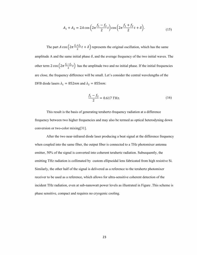
After the two near-infrared diode laser producing a beat signal at the difference frequency
when coupled into the same fiber, the output fiber is connected to a THz photomixer antenna
emitter, 50% of the signal is converted into coherent terahertz radiation. Subsequently, the
emitting THz radiation is collimated by custom ellipsoidal lens fabricated from high resistive Si.
Similarly, the other half of the signal is delivered as a reference to the terahertz photomixer
receiver to be used as a reference, which allows for ultra-sensitive coherent detection of the
incident THz radiation, even at sub-nanowatt power levels as illustrated in Figure .This scheme is
phase sensitive, compact and requires no cryogenic cooling.
24
Figure 12: Schematic of the fiber coupled CW THz spectrometer.
Spectroscopy is achieved by incrementally varying the difference frequency via a
temperature-tuning technique using a smooth, mode-hop free tuning of the near-infrared diode
lasers. The signal amplitude and phase are measured at each discrete frequency point, from which
the power can be derived. At each frequency point in the spectrum, a sinusoidal waveform is
acquired using a time domain sweep, executed using fiber stretching technology. The nominal
spectral resolution is governed by the precious of the laser frequency control, and on average can
be as low as 100MHz. Whereas the time-domain spectroscopy (TDS) THz system which many
group using are limited by a mechanical delay stage. After Fourier transforming, the
corresponding frequency resolution can be as high as 58.8 GHz[34], which is only half of the CW
spectra 400. Thus, the CW spectra 400 is an ideal choice for resolving high Q-factor spectral
features with metamaterials and low-frequency bond vibrations.
25
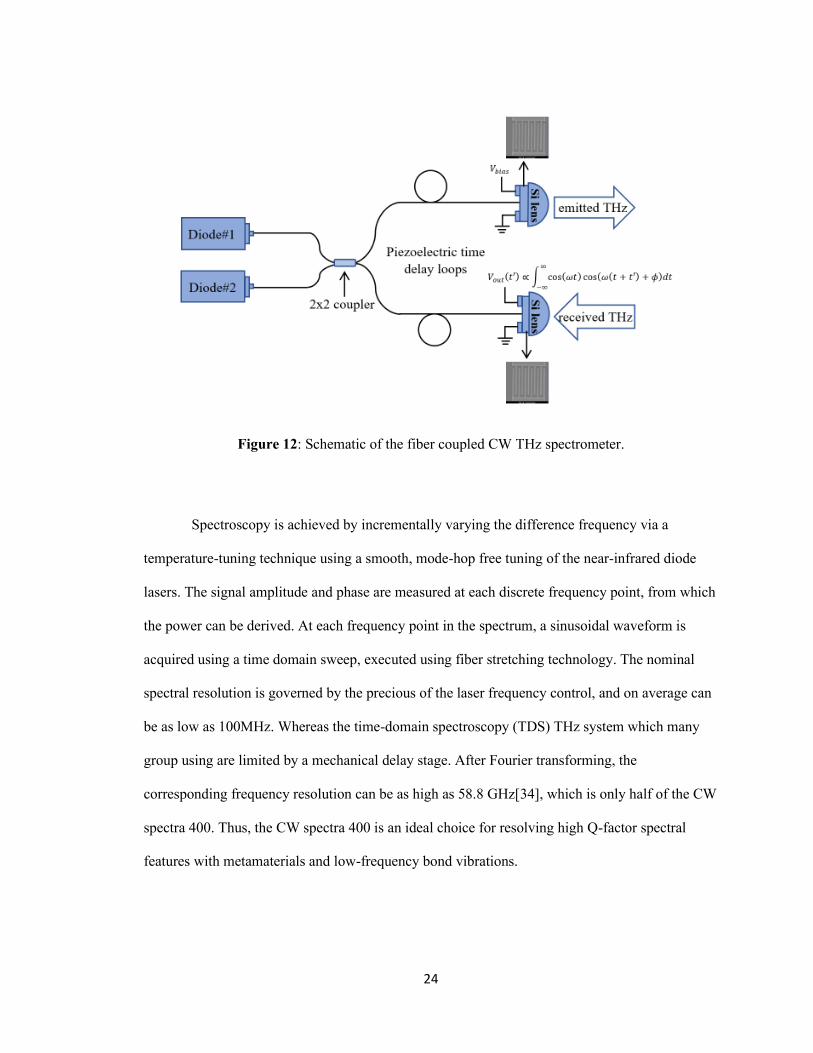
Figure 13: The schematic of the THz CW spectroscopy
The associated software of the Spectra 400 alignment can be achieved by maximizing the
power at a fixed frequency. The distance between emitter and receiver is 𝑑 = 12 𝑐𝑚 as shown
in figure 13. The sample will be attached to a rotatable holder and be placed in the midpoint when
used for transmission measurement. The samples can be rotated to mimic different polarization
states. Before the sample can be measured, the background measurement is necessary. By
performing 2-3 times background measurement, the transmission result will change gradually,
when the data become steady, which means doesn’t change compared to the last time
measurement, the spectrometer is warm up properly and ready to work on sample. The
background measurement will also be a reference for the later data analyzing.
If we want to investigate the transmission property of MoS2 layer ,the sample substrate
measurement can also be used as a background measurement. The process will keep same, only
the reference data change to the measurement from substrate.
3.1.4 Data Analysis
The CW software is intended for instrument control and data collection. At each
incremental frequency step the system records the real and imaginary electric fields. To produce
26
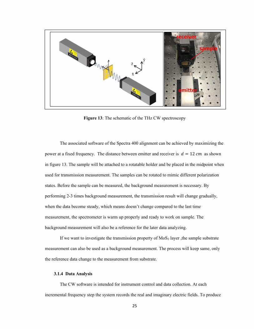
readable data, an effective data post processing analysis must be conducted. Figure shows the
power spectra of air with the raw to the smoothed data. The data is smoothed by doing
convolution with a defined length of matrix made with one. The length can be changed to meet
different condition, to get a smoother graph, the filter matrix length can increase, to get a nosier
graph, this filter should be decreased.
Figure 14: THz Power spectrum of air in the test area with water features labeled
The features in the frequency range from 1.1 to 1.2 THz, the two frequency 𝑓1 = 1.1 𝑇𝐻𝑧
and 𝑓2 = 1.17 𝑇𝐻𝑧 are arise from the water molecules presented in the moist, which is agree with
the water vapor frequencies reported by van Exter et. al.[33]. The impact of water features can be
removed when calculating the transmission T which is obtained by using the following
relationship:
1.00E-05
1.00E-04
1.00E-03
1.00E-02
1.00E-01
1.00E+000.1 0.3 0.5 0.7 0.9 1.1
TH
z P
ow
er(a
.u.)
Frequency (THz)
Raw Data
Smoothed Data
f1f2
27
𝑇(𝑣) =
𝑃𝑠𝑎𝑚𝑝𝑙𝑒(𝑣)
𝑃𝑟𝑒𝑓𝑒𝑟𝑒𝑛𝑐𝑒(𝑣)
(17)
Where 𝑃𝑠𝑎𝑚𝑝𝑙𝑒(𝑣) and 𝑃𝑟𝑒𝑓𝑒𝑟𝑒𝑛𝑐𝑒(𝑣) are the filtered power of the sample and reference.
The PDMS substrate was used for the reference measurement during characterization.
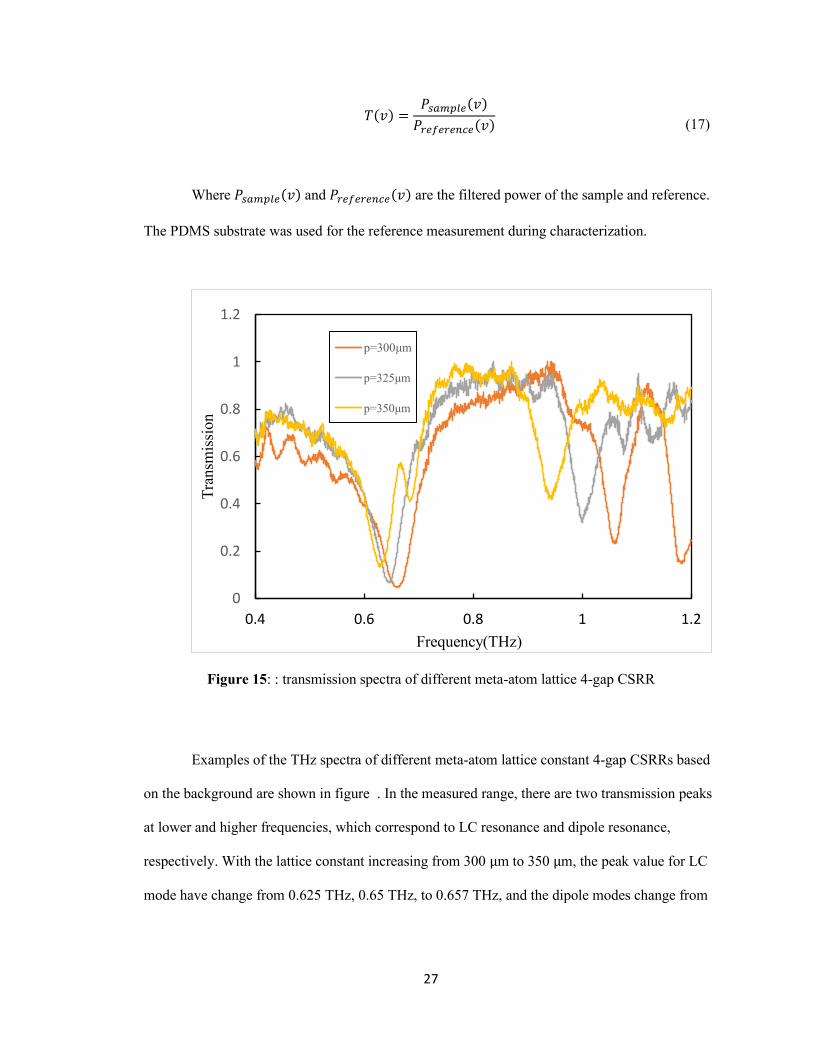
Figure 15: : transmission spectra of different meta-atom lattice 4-gap CSRR
Examples of the THz spectra of different meta-atom lattice constant 4-gap CSRRs based
on the background are shown in figure . In the measured range, there are two transmission peaks
at lower and higher frequencies, which correspond to LC resonance and dipole resonance,
respectively. With the lattice constant increasing from 300 µm to 350 µm, the peak value for LC
mode have change from 0.625 THz, 0.65 THz, to 0.657 THz, and the dipole modes change from
0
0.2
0.4
0.6
0.8
1
1.2
0.4 0.6 0.8 1 1.2
Tra
nsm
issi
on
Frequency(THz)
p=300μm
p=325μm
p=350μm
28
0.94 THz, 0.99 THz and 1.05 THz, respectively. The Q-factor which is a universally metric to
characterize spectral features of metamaterials is defined as:
𝑄 =𝑣0
∆𝑣
(18)
Where 𝑣0 is the resonant frequency and ∆𝑣 is the full width half maximum (FWHM) of
the resonance frequency. In this measurement, the FWHM of three different constant are
0.095THz, 0.102THz and 0.072 THz, so that the corresponding Q factor are 0.152, 0.157 and
0.11.
3.1.5 Finite Element Method Simulations
To do the further studies of the MMs, the finite element method (FEM) is used to analyze
the spectral response of a unit cell. Because of the complicated geometries and material
properties, the analytical solutions of ordinary or partial differential equations are not usually
obtainable. Hence we need to rely on numerical methods, such as the finite element method in
this case. The finite element formulation of the problem, rather than requiring to solve the
differential equations, but results in a system of simultaneous algebraic equations for solution.
Instead of solving the problem for the entire body in operation, the FEM formulate the equations
for each finite element and combine them to obtain the solution of the whole body[44]. By using
the built-in geometry tools in COMSOL, the metasureface of each unit cell in three-dimensional
spatial domain was constructed. The parameter dimension can be changed for different shape of
resonator. In these numerical calculations, normally THz plane wave of a particular polarization
illuminate on the elementary cell of the designed planar MM, via port boundary conditions. To
mimic a two-dimensional structure, the periodic floquet boundary conditions were imposed to
each device.
29
The mesh settings determine the resolution of the finite element mesh used to discretize
the model. The finite element method divides the model into small part of geometrically simple
shapes. In the case of tetrahedrons mesh, a ‘non-manifold’ simulation model is created. In each
tetrahedron, series of polynomial functions are used to approximate different parameters based on
the selected physics module. The electromagnetic wave was selected under the wave optics
module which provides the electric field, magnetic field and surface current distributions after a
frequency sweep over the frequency range. And the transmission was calculated by square of the
S21 parameter.
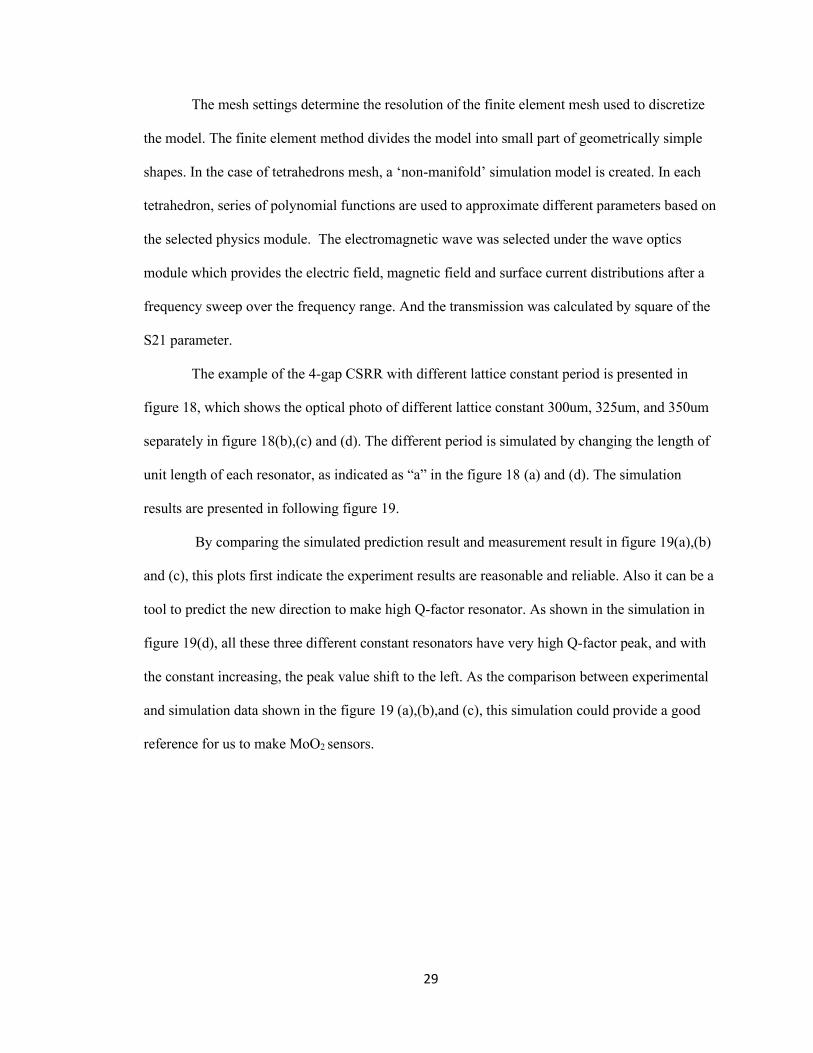
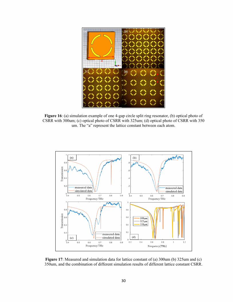
The example of the 4-gap CSRR with different lattice constant period is presented in
figure 18, which shows the optical photo of different lattice constant 300um, 325um, and 350um
separately in figure 18(b),(c) and (d). The different period is simulated by changing the length of
unit length of each resonator, as indicated as “a” in the figure 18 (a) and (d). The simulation
results are presented in following figure 19.
By comparing the simulated prediction result and measurement result in figure 19(a),(b)
and (c), this plots first indicate the experiment results are reasonable and reliable. Also it can be a
tool to predict the new direction to make high Q-factor resonator. As shown in the simulation in
figure 19(d), all these three different constant resonators have very high Q-factor peak, and with
the constant increasing, the peak value shift to the left. As the comparison between experimental
and simulation data shown in the figure 19 (a),(b),and (c), this simulation could provide a good
reference for us to make MoO2 sensors.
30
Figure 16: (a) simulation example of one 4-gap circle split ring resonator, (b) optical photo of
CSRR with 300um; (c) optical photo of CSRR with 325um; (d) optical photo of CSRR with 350
um. The “a” represent the lattice constant between each atom.
Figure 17: Measured and simulation data for lattice constant of (a) 300um (b) 325um and (c)
350um, and the combination of different simulation results of different lattice constant CSRR.
𝑎
𝑎
(a) (b)
(c) (d)
31
3.2 Material
In this section, the material the MMs composition and the substrate will be investigated.
First, the supporting substrate properties will be discussed. After that, the properties of samples
made with different combinations of substrate thickness and different annealing different laser
power on amorphous MoS2 will be discussed.
3.2.1 Substrate Investigations
To fabricate a flexible sensor, the physical properties for the substrate of our
metamaterial is very important. First of all, the material should be flexible. Also, the substrate
should not be highly absorptive or reflective in THz range. In our case, we investigate three
different substrate: 100um and 500um willow glass and 50um PDMS.
The effect can be understood as the Fabry-Perot(FP) interferometer, which have two flat
and parallel semi-transparent mirrors. The resonant frequency can be written as:
𝑣𝑞 = 𝑞𝑐
2𝑛𝑑, 𝑓𝑜𝑟 𝑛 = 1,2,3, .. (19)
Where c is the speed of light and d is the thickness of the sample. This also predicts the
transmission peak position. By changing the substrate thickness form 500 µm to 100 µm, the
fringe increase from 0.13 THz to 0.65 THz which is five times larger.
32
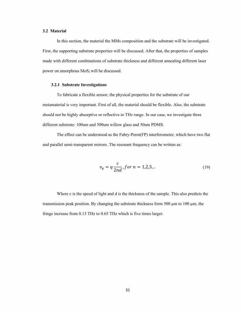
Figure 18: Transmission spectra of (a) 500 µm, (b) 100 µm thick willow glass.
It can be read from the figure 20, that the fringes at thick willow glass are 0.15THz,
0.12THZ,0.15THz and 0.14THz, has the average of 0.14 THz which is similar to 0.13 THz as
expected. And the fringe in thin willow glass is 0.65 THz, which is exactly same with expected.
The experiment result shows great fitting with the theoretically prediction.
Now the PDMS transmission measurement results are added, and plot these in a same
graph, the result shows:
0
0.1
0.2
0.3
0.4
0.5
0.6
0.7
0.8
0.9
1
0.2 0.45 0.7 0.95 1.2
Tra
nsm
issi
on
Frequency (THz)0.2 0.45 0.7 0.95 1.2
Frequency(THz)
(a) (b)
33
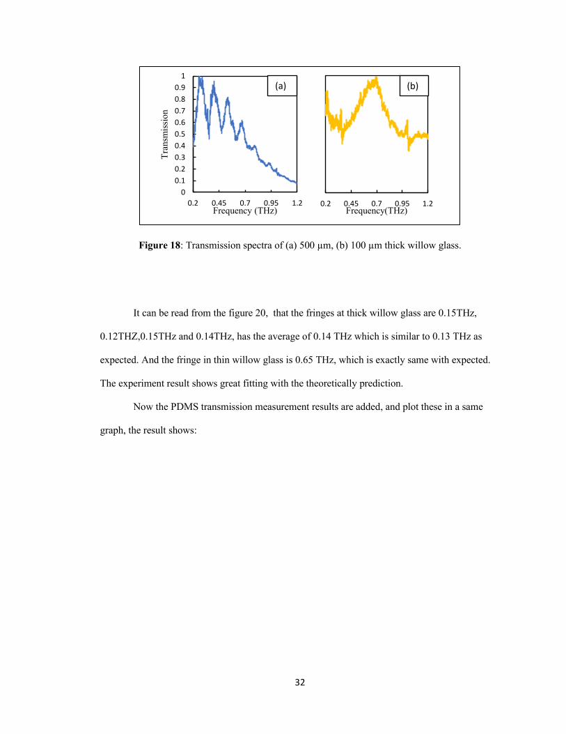
Figure 19: transmission curve for three different substrates
Figure 21 shows all the transmission spectra of the potential substrates. In the term of the
properties, the thin glass has the best transmission properties above 0.8 THz, compare to the thick
glass and PDMS. The thick glass substrate and PDMS substrates are more lossy in the higher
regime, but still a usable range. Considering the big oscillation of thick glass in the lower
frequency range, it’s not a good substrate to use. The PDMS and thin willow glass will be the
substrate candidates. Since the thin willow glass has the better transmission in the higher
frequency range, this will be used as the material through this project.
3.2.2 Raman Characterization
The Raman spectroscopy is used to characterize the annealing result of substrate under
different laser power and scanning speed, which relies upon Raman scattering and gives
information about vibrations within a molecule. The spectrum of the scattered photons is referred
as the Raman spectrum, which shows the intensity of the scattered light as the function of the
frequency different between the incident photons and scattered photons and are more commonly
0
0.2
0.4
0.6
0.8
1
1.2
0.2 0.4 0.6 0.8 1 1.2
Tra
nsm
issi
on
Frequency(THz)
Thick Glass
Thin Glass
PDMS
34
called Raman shift. On the other words, Raman spectroscopy is a result of molecular vibrations
which bring a change in the polarizability of a material. Therefore periodic vibrations are
necessary for Raman spectroscopy operation mechanisms.
Before the sensor can be really fabricated, the material properties under different
fabrication condition should be measured first, since the results are highly sensitive to different
annealing conditions. To be specific, the laser intensity, the scanning speed and the substrate
thickness are the three main factors in our experiment. In this section, the precursor samples will
be characterized via Raman spectroscopy to make sure the transformation between different
phases. All Raman spectra will be taken at the center of each laser-modified region.
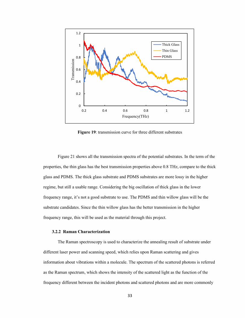
The first precursor sample will be amorphous MoS2 samples on 500um thickness willow
glass. The corresponding picture of the annealed region is shown in the Figure 20.
Figure 20: Fabricated line precursor sample
35
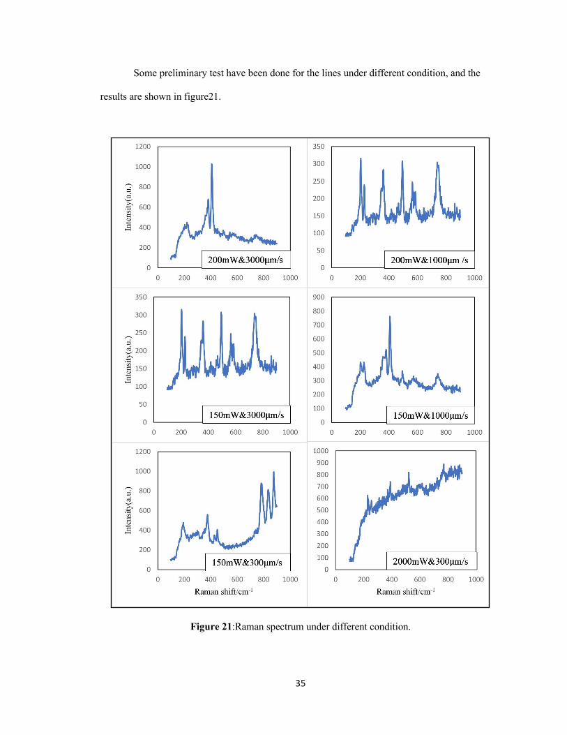
Some preliminary test have been done for the lines under different condition, and the
results are shown in figure21.
Figure 21:Raman spectrum under different condition.
36
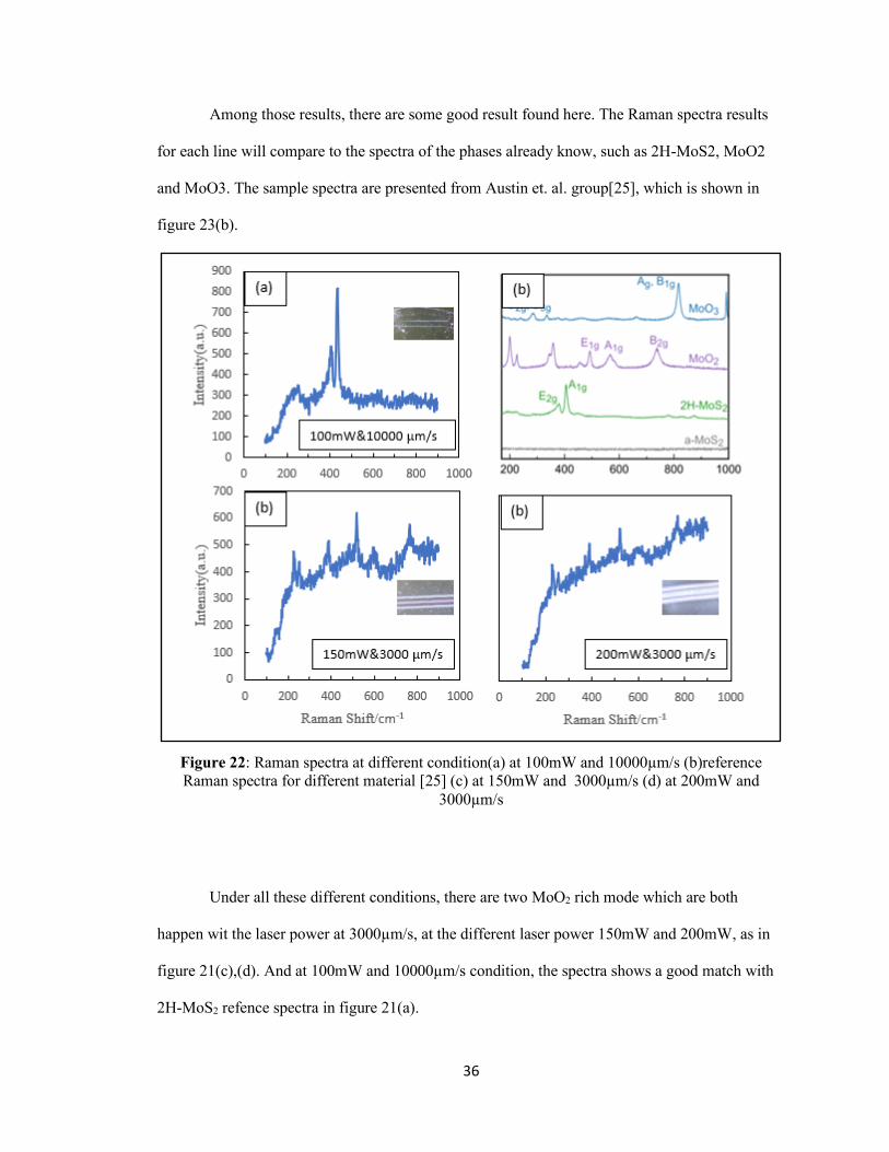
Among those results, there are some good result found here. The Raman spectra results
for each line will compare to the spectra of the phases already know, such as 2H-MoS2, MoO2
and MoO3. The sample spectra are presented from Austin et. al. group[25], which is shown in
figure 23(b).
Figure 22: Raman spectra at different condition(a) at 100mW and 10000µm/s (b)reference
Raman spectra for different material [25] (c) at 150mW and 3000µm/s (d) at 200mW and
3000µm/s
Under all these different conditions, there are two MoO2 rich mode which are both
happen wit the laser power at 3000µm/s, at the different laser power 150mW and 200mW, as in
figure 21(c),(d). And at 100mW and 10000µm/s condition, the spectra shows a good match with
2H-MoS2 refence spectra in figure 21(a).

37
Due to the higher conductivity, the MoO2 will be chosen as the annealing part material.
The 150mW and 3000µm/s combination will be chosen to use in our sensor fabrication since
higher speed goes shorter fabrication time.
38
CHAPTER IV
DEVICE CHARACTERIZATION
4.1 4-gap SSRR simulation
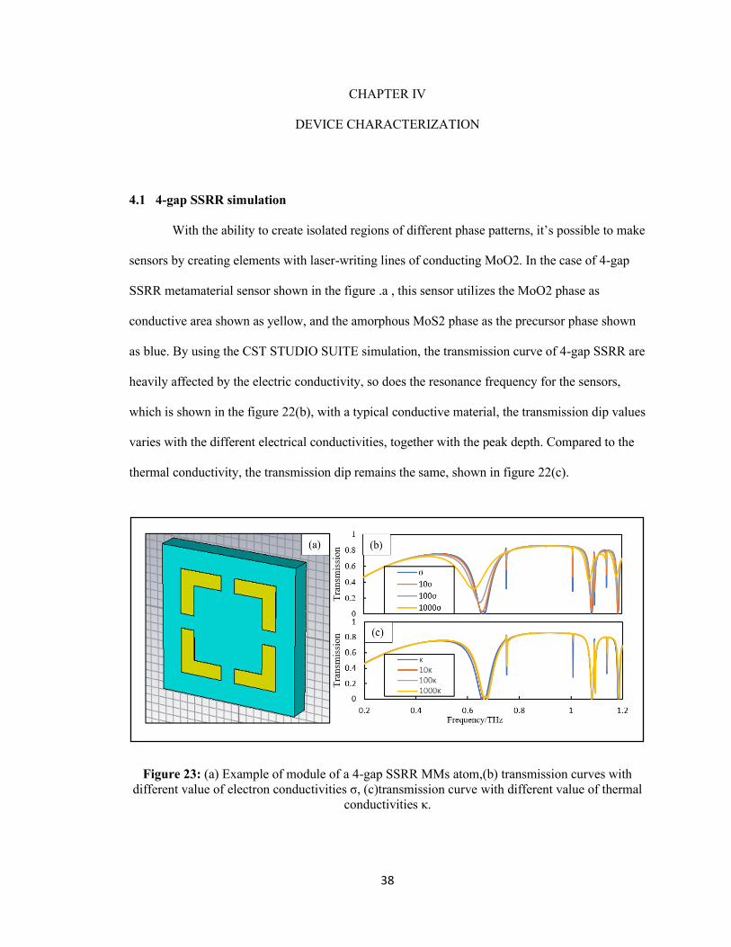
With the ability to create isolated regions of different phase patterns, it’s possible to make
sensors by creating elements with laser-writing lines of conducting MoO2. In the case of 4-gap
SSRR metamaterial sensor shown in the figure .a , this sensor utilizes the MoO2 phase as
conductive area shown as yellow, and the amorphous MoS2 phase as the precursor phase shown
as blue. By using the CST STUDIO SUITE simulation, the transmission curve of 4-gap SSRR are
heavily affected by the electric conductivity, so does the resonance frequency for the sensors,
which is shown in the figure 22(b), with a typical conductive material, the transmission dip values
varies with the different electrical conductivities, together with the peak depth. Compared to the
thermal conductivity, the transmission dip remains the same, shown in figure 22(c).
Figure 23: (a) Example of module of a 4-gap SSRR MMs atom,(b) transmission curves with
different value of electron conductivities σ, (c)transmission curve with different value of thermal
conductivities κ.
39
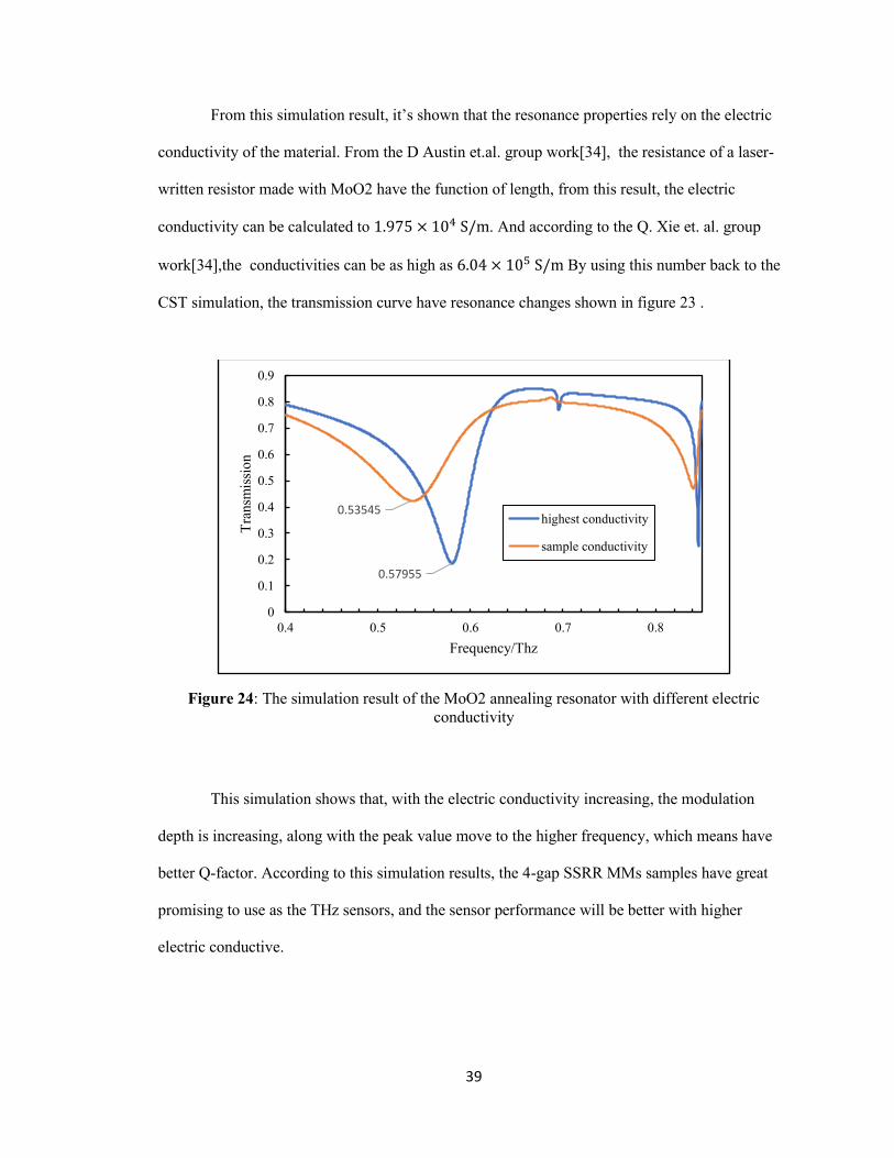
From this simulation result, it’s shown that the resonance properties rely on the electric
conductivity of the material. From the D Austin et.al. group work[34], the resistance of a laser-
written resistor made with MoO2 have the function of length, from this result, the electric
conductivity can be calculated to 1.975 × 10⁴ S/m. And according to the Q. Xie et. al. group
work[34],the conductivities can be as high as 6.04 × 10⁵ S/m By using this number back to the
CST simulation, the transmission curve have resonance changes shown in figure 23 .
Figure 24: The simulation result of the MoO2 annealing resonator with different electric
conductivity
This simulation shows that, with the electric conductivity increasing, the modulation
depth is increasing, along with the peak value move to the higher frequency, which means have
better Q-factor. According to this simulation results, the 4-gap SSRR MMs samples have great
promising to use as the THz sensors, and the sensor performance will be better with higher
electric conductive.
0.57955
0.53545
0
0.1
0.2
0.3
0.4
0.5
0.6
0.7
0.8
0.9
0.4 0.5 0.6 0.7 0.8
Tra
nsm
issi
on
Frequency/Thz
highest conductivity
sample conductivity

40
4.2 4-gap SSRR fabrication
By setting the resonator arm width and the gap to be 35um, the square side length to be
250 µm, and the lattice constant to be 320µm. From previous line characterization, the line width
of MoO2 region is around 8um.
In the fabrication process, first we will create an array composed with x position, y
position, move direction, length, laser power and move speed. Then we use the generated array
to control the system, such as the motion stage moving condition and the shutter status, to
fabricate the samples. The position of the motion stage is calculated and transferred to the
mechanical step size, so it can read and follow each number in this array to move.
However, due to the current situation, work has been interrupted and didn’t get the good
results yet. Hopefully this result could finish soon.
41
CHAPTER V
SUMMARY AND CONCLUSIONS
5.1 Conclusion
In conclusion, we have constructed a fabrication system which utilize the laser annealing
process to fabricated metamaterial THz sensors composed with resonators on the micrometer
range using MoS2. Some experiment using this system to fabricate lines have been successful, but
there is no resonator array fabricated successfully yet.
Laser lines with different laser power and moving speed are characterized by Raman
spectroscopy system. According to the Raman spectroscopy result, the combination of 150mW
and 200mW laser power and 3000 µm/s moving speed shows best fitting with the MoO2 Raman
spectroscopy record before, which means under this condition, it is more likely to get MoO2
phases, which is most conducting and more suitable to make resonators.
The optical image of the fabricated using the system shows the pattern is either not
straight or not the pattern we desired. The problem might be the code controlling the moving
stage, the system will be able to use soon after the code is fixed.
After the resonator array are successfully fabricated, sensor on different substrate should
be conducted, with the best laser power and moving speed combination regarding to the thin
willow glass substrate to be determined.
5.2 Future work
There are two parts of work which should be done in the future to finish this project. The
first part is to increase the stable of the system. And the second part is to further improving and
use this system to fabricate sensor, test sensors and further improve the sensor responsivity.
42
To increase the stable of laser writing system, there are several things can be done. The
first is replacing the photodiode into the power meter. Since the photodiode is too unstable, the
output results can varies a lot by changing a small amount of angle. This will make the power
reading result not correct and thus affect the final annealing results, such as the MoS2 phases, or
the MoO2 line width.
The other thing needs to make sure is the shutter speed. Since the dimension of sample
we are making are around micrometer. And the speed are usually 3000 um/s, which makes the
shutter reaction time only several milliseconds. If the shutter moves slower than the motion stage
moving, the pattern might change with misalignment between shutter and motion stage.
As for the future working using this system, there’s lots of possibilities. If he 4-gap SSRR
resonator array is fabricated successfully, then the pattern can be changed with needs to create the
sensors which have the desired features. Or the other asymmetric or different shape of resonator
can be also done in this system easily.
Finally, the fabricated sensors can be tested with biological or chemical material, if these
can work smoothly, this easy-making flexible sensors can be used on wearable devices on an
affordable cost.
43
BIBLIOGRAPHY
1. K.E. Sapsford, C. Bradburne, J.B. Delehanty, and I. L. Medintz. "Sensors for detecting
biological agents," Materials today , vol.11, no. 3, pp.38-49,2008.
2. M. Burnworth, S.J. Rowan, C. Weder, “Fluorescent sensors for the detection of chemical
warfare agents.” Chemistry–A European Journal, vol.13, no.28, pp.7828-7836,2007.
3. S. Zeng, D. Baillargeat, H. P. Ho, K. T. Yong, “Nanomaterials enhanced surface plasmon
resonance for biological and chemical sensing applications.” Chemical Society
Reviews, vol.43, no.10, pp.3426-3452, 2014.
4. McConney, et. al. "Direct synthesis of ultra-thin large area transition metal
dichalcogenides and their heterostructures on stretchable polymer surfaces," Journal of
Materials Research ,vol.31, no.7, pp.967-974, 2016.
5. Wang, et. al. "Transmittance and sheet conductivity of monolayer WS2 measured by
terahertz spectroscopy," 2017 10th UK-Europe-China Workshop on Millimetre Waves
and Terahertz Technologies (UCMMT). IEEE,2017.
6. Bukhari, et. al. "A metasurfaces review: Definitions and applications." Applied
Sciences ,vol.9, no.13, p.2727, 2019.
7. Böker, Th, R. Severin, A. Müller, C. Janowitz, R. Manzke, D. Voß, P. Krüger, A. Mazur,
and J. Pollmann. "Band structure of MoS2, MoSe2, and α− MoTe2: Angle-resolved
photoelectron spectroscopy and ab initio calculations," Physical Review B 64, no. 23, p.
235305,2001.
8. X. Duan, C. Wang, A. Pan, R. Yu, X. Duan, “Two-dimensional transition metal
dichalcogenides as atomically thin semiconductors: opportunities and challenges,”
Chemical Society Reviews, vol.44, no.24, pp. 8859- 8876, 2015.
44
9. Akinwande, Deji, N. Petrone, and J. Hone. "Two-dimensional flexible
nanoelectronics," Nature communications , vol.5, no. 1, pp.1-12,2014.
10. Burrow, Joshua Anthony, 4-Gap Asymmetric Terahertz Metasurfaces, Diss. University
of Dayton, 2017.
11. V.G.Veselago,”The Electrodynamics of Substances with Simulaneously Negative Values
of ε and µ,“Soviet Physics Uspekhi, vol. 10, no.4, p.509, 1968.
12. Yen, et. al. "Terahertz magnetic response from artificial materials." Science , vol.303, no.
5663, pp. 1494-1496, 2004.
13. X. Chen and W. Fan, “Study of interaction between graphene and planar terahertz
metamaterial with toriodal dipolar resonance,” Opt. Letters, vol. 42, no. 10, 2017.
14. J. B. Pendry, A. J. Holden, D. J. Robbins, and W. J. Stewart, “Magnetism from
conductors and enhanced nonlinear phenomena,” IEEE Trans. Microw. Theory Techn.,
vol. 47, no. 11, pp.2075–2084, 1999.
15. I. Al-Naib, Y. Yang, M. M. Dignam, W. Zhang, and R. Singh, “Ultra-high q even
eigenmode resonance in terahertz metamaterials,” Appl. Phys. Lett., vol. 106, no. 011102,
2015.
16. R. A. Shelby, D. R. Smith, S. Schultz, ”Experimental verification of a negative index of
refraction, “Science, vol. 292, no. 5514, pp. 77–79, 2001.
17. A. K. Iyer and G. V. Eleftheriades, “Free-space imaging beyond the diffraction limit
using aveselago-pendry transmission-line metamaterial superlens,” IEEE Trans.
Antennas Propag.,vol. 57, no. 6, pp. 1720–1727, Jun 2009.
18. Z. Zhao, X. Zheng, W. Peng, H. Zhao, J. Zhang, Z. Lou, and W. Shi, “Localized slow
light phenomenon in symmetry broken terahertz metamolecule made of conductively
coupled dark resonators,” Opt. Mater. Express, vol. 7, no. 6, pp. 1950–1961,2017.
45
19. X. Chen, W. Fan, “Study of interaction between graphene and planar terahertz
metamaterial with toroidal dipolar resonance,” Opt. Letters, vol. 42, no. 10, 2017.
20. I. Al-Naib, C. Jansen, and M. Koch, “High q-factor metsurfaces based on miniaturized
asymmetric single split resonators,” Appl. Phys. Lett., vol. 94, p.153505, 2009.
21. R. Singh, I. A. I. Al-Naib, M. Koch, and W. Zhang, “Asymmetric planar terahertz
metamaterials,”Opt. Express, vol. 18, no. 12, pp. 13044–13050, 2010.
22. C. Jansen, I. A. Al-Naib, N. Born, and M. Koch, “Terahertz metasurfaces with high q-
factors,” Appl. Phys. Lett., vol. 98, no. 051109, 2011.
23. L. Cong, M. Manjappa, N. Xu, I. Al-Naib, W. Zhang, and R. Singh, “Fano resonances in
terahertz metasurfaces: A figure of merit optimization,” Adv. Optical Mater., pp. 1537–
1543,2015.
24. Akinwande, et. al "Two-dimensional flexible nanoelectronics," Nature
communications ,vol.5, no.1, pp.1-12, 2014.
25. Drake Austin, et.al.,” Transformative Manufacturing: Laser Writing Electronic Circuitry
in Thin Film Molybdenum Disulfide,” submitted to Materials Today,2020
26. Y. Shigegaki, S. Basu, M. Wakihara, M. Taniguchi, “Thermal analysis and kinetics of
oxidation of molybdenum sulfides,” Journal of Thermal Analysis and Calorimetry, vol.
34, no.5-6, pp.1427-1440,1988.
27. R. F. Sebenik, A. R. Burkin, R.R. Dorfler, J.M. Laferty, G. Leichtfried, H. Meyer-
Grunow, P.C. Mitchell, et. al., “Molybdenum and molybdenum compounds,” Ullmann's
Encyclopedia of Industrial Chemistry,2000.
28. Wilkomirsky, I., Otero, A., Balladares, E. “ Kinetics and reaction mechanisms of high-
temperature flash oxidation of molybdenite,” Metallurgical and Materials Transactions
B, vol,41, no.1, pp.63-73, 2010.
46
29. M. E. McConney, N. R. Glavin, A.T. Juhl, M. H. Check, M. F. Durstock, A. A.
Voevodin, M. K. Gupta, “Direct synthesis of ultra-thin large area transition metal
dichalcogenides and their heterostructures on stretchable polymer surfaces,” Journal of
Materials Research, vol.31, no.7, pp.967-974, 2016.
30. TeraView, CW Spectra 400, TeraView, 2010.
31. R. Lewis, Terahertz Physics, Cambridge University Press, 2012.
32. R. Yahiaoui, S. Tan, L. Cong, R. Singh, F. Yan, and W. Zhang, “Multispectral terahertz
sensing with highly flexible ultrathin metamaterial absorber,” J. Appl. Phys., vol. 118, p.
083103, 2015.
33. M. van Exte, C. Fattinger, and D. Grischkowsky, “Terahertz time-domain spectroscopy
of water vapor,” Opt. Letters, vol. 14, no. 20, 1989.
34. X. Qiliang, Z. Xiaoming, D. Wu, X. Chen, Jiao Shi, X. Han, X. Zhang, G. Peng, Y.Gao,
and Han Huang, "High electrical conductivity of individual epitaxially grown MoO2
nanorods," Applied Physics Letters , vol.111, no. 9, p.093505, 2017.


![[Transformative Immersion]](https://img.pdfslide.net/doc/110x75/63323fc2ac2998afa70a1ae8/transformative-immersion.jpg)


