Embed Size (px)
Citation preview

Single-photon Detectors Based on InP Avalanche Diodes: Status and Prospects
Mark A. Itzler*, Xudong Jiang, Mark Entwistle, Bora M. Onat, Krystyna Slomkowski
Princeton Lightwave Inc., 2555 US Route 130 South, Cranbury, NJ 08512
ABSTRACT
We report on progress in improving fundamental properties of InP-based single photon avalanche diodes (SPADs) and recent trends for overcoming dominant performance limitations. Through experimental and modeling work focused on the trade-off between dark count rate (DCR) and photon detection efficiency (PDE), we identify the key mechanisms responsible for DCR over a range of operating temperatures and excess bias voltages. This work provides a detailed description of temperature- and bias-dependent DCR thermal activation energy Ea(T,V), including the crossover from low Ea for trap-assisted tunneling at temperatures below ~230 K to larger Ea for thermal generation at temperatures approaching room temperature. By applying these findings to new device design and fabrication, the fundamental tradeoff between PDE and DCR for InP/InGaAs SPADs designed for 1.55 µm photon detection has been managed so that for PDE ~ 20%, devices routinely exhibit DCR values of a few kHz, while “hero” devices demonstrate that it is possible to achieve sub-kHz DCR performance at temperatures readily accessible using thermoelectric coolers. However, important limitations remain, particularly with respect to maximum count rates. Strategies adopted recently to circumvent some of these present limitations include new circuit-based solutions involving high-speed very short-duration gating as well as new monolithic chip-level concepts for obtaining improved performance through avalanche self-quenching. We discuss these two approaches, and we describe recent results from devices with monolithically integrated quench resistors that achieve rapid self-quenching, accompanied by evidence for a partial discharge of the detector capacitance leading to charge flows as low as ~3 ×10⁵ carriers associated with each avalanche event. Keywords: avalanche photodiode, single photon detector, SPAD, Geiger mode, negative feedback, InP, InGaAsP
1. INTRODUCTION Single photon detectors based on avalanche diode structures are frequently the best choice for applications requiring high performance, high reliability, ease of implementation, and scalability. In the past several years, we have made significant progress for certain properties of InP-based single photon avalanche diodes (SPADs). For instance, the fundamental tradeoff between photon detection efficiency (PDE) and dark count rate (DCR) in InP/InGaAs SPADs designed for 1.55 µm photon detection routinely exhibits DCR values of a few kHz for PDE ~ 20%, and “hero” devices achieve sub-kHz DCR performance at temperatures readily accessible using thermoelectric coolers. High precision timing jitter has also been demonstrated for these detectors, with 100 ps jitter found for typical operating conditions, and 50 ps or less obtained for sufficiently high excess bias. However, important limitations remain, particularly with respect to maximum count rates. Although intrinsic SPAD response is fast, with avalanche build-up occuring in well under 1 ns, afterpulsing effects have often limited counting rates to the range of 1 to 10 MHz. Recent strategies for surmounting counting rate limitations have focused on two distinct approaches. The first approach entails the use of improved electronic circuitry for limiting current flow per avalanche, usually by invoking very short-duration gated quenching. Although these techniques are usually limited to periodic short-gate operation, they have demonstrated dramatic increases in gate repetition rate to the GHz range. The second strategy encompasses chip-level concepts for obtaining improved performance through avalanche self-quenching by the monolithic integration of negative feedback elements to achieve dramatic reduction in the charge flow per avalanche. In the latter part of this paper, we present recent results from one class of these “negative feedback” avalanche diodes (NFADs) with monolithically integrated quench resistors. The phenomenal industrial growth of fiber optic telecommunications through the 1990s fueled tremendous advances in the design and performance of InP-based avalanche photodiodes (APDs) for the near-infrared wavelength range from * [email protected], tel: (609)495-2551, fax: (609)395-9113
Advanced Photon Counting Techniques IV, edited by Mark A. Itzler, Joe C. Campbell,Proc. of SPIE Vol. 7681, 76810V · © 2010 SPIE · CCC code: 0277-786X/10/$18
doi: 10.1117/12.852705
Proc. of SPIE Vol. 7681 76810V-1
Downloaded from SPIE Digital Library on 12 May 2010 to 128.59.62.83. Terms of Use: http://spiedl.org/terms

1.0 to 1.7 μm. However, since traditional APD-based fiber optic receivers require “linear mode” operation, for which the output photocurrent is proportional to the input optical power, these advances were directed exclusively at improvements in low-gain linear mode APD performance. In contrast, the detection of single photons using APDs is accomplished by operating devices in the so-called “Geiger mode”, in which a single photon can trigger a macroscopic current pulse that can be sensed with a digital threshold detection circuit. Historically, researchers who had sought detectors with good Geiger mode performance were forced to adopt the hit-or-miss strategy of sampling the various commercially available telecom APDs and characterizing their Geiger mode behavior with the hope of obtaining good single photon detectors [1–5]. For the last several years, we have focused on the design and commercialization of avalanche diodes intended specifically for high-performance single photon detection. As we have described previously [6], the optimization of InP-based SPADs for detecting single photons is quite distinct from the optimization of APDs for linear mode performance, primarily because critical linear mode attributes (such as excess noise and gain-bandwidth product) are irrelevant for SPADs. SPADs are avalanche diode structures designed to operate above their breakdown voltage Vb, so that a single photoexcited carrier can induce a macroscopic current by avalanche breakdown. Applying a reverse bias Va > Vbr places the avalanche diode in a metastable state in which a single free carrier can initiate a self-sustaining runaway avalanche. Strictly speaking, the concept of gain is no longer relevant when discussing Geiger-mode operation, and it is more appropriate to think of a SPAD as a photon-activated switch. The runaway avalanche leads to a macroscopic current pulse that can be sensed using an appropriate threshold detection circuit. Biasing and detection circuitry can be realized using several different schemes, but they all involve taking the SPAD from an “idle” bias Vi below breakdown (i.e., Vi < Vbr) to an applied bias Va that exceeds breakdown by the excess bias (i.e., ΔV = Va - Vbr) and puts the device into its “armed” state in which it can detect the arrival of a single photon. Gated bias circuits employ excess bias voltages for a fixed period of time so that the device is armed for a pre-determined duration and then disarmed by removing the excess bias.
2. DESIGN OF AVALANCHE DIODES FOR SINGLE PHOTON DETECTION All InGaAs/InP avalanche photodetectors commercially deployed today are based on a separate absorption and multiplication (SAM) region epitaxial structure [7], and the same holds true for SPADs. This design employs a narrow bandgap In0.53Ga0.47As absorption layer [Eg,InGaAs(295 K) ~ 0.75 eV] lattice-matched to InP to absorb photons with the wavelength of interest (e.g., 1.5 μm), adjacent to a wider bandgap InP region [Eg,InP(295 K) ~ 1.35 eV] in which avalanche multiplication occurs. In Figure 1, we present a schematic representation of our basic device design platform.
Figure 1. Cross-sectional schematic of the single photon avalanche diode design platform. The electric field profile at right corresponds to a path through the active region of the device, as indicated by the dotted line.
n+-InP buffer
n-InGaAsP gradingn-InP charge
i-InP cap
SiNx passivationanode contact
anti-reflection coating cathode contact
optical input
Electric field
i-InGaAs absorption
multiplication region
p+-InP diffused region
n+-InP substraten+-InP buffer
n-InGaAsP gradingn-InP charge
i-InP cap
SiNx passivationanode contact
anti-reflection coating cathode contact
optical input
Electric field
i-InGaAs absorption
multiplication region
p+-InP diffused region
n+-InP substrate
Proc. of SPIE Vol. 7681 76810V-2
Downloaded from SPIE Digital Library on 12 May 2010 to 128.59.62.83. Terms of Use: http://spiedl.org/terms

The lateral structure of our SPAD design employs a buried p-n junction to guarantee edge breakdown suppression, low perimeter leakage, and high reliability. The use of this platform for the fabrication of commercial linear mode APDs is described elsewhere [8]. 2.1 Numerical modeling of dark count rate A quantitative description of SPAD behavior requires models for the generation of carriers that can trigger avalanche breakdown and for the avalanche process itself. We use McIntyre’s standard formulations for calculating the breakdown voltage[9] and avalanche probability Pa above breakdown [10]. These calculations require expressions for the impact ionization coefficients α(T) and β(T), and we have adopted the formulas derived by Zappa, et al. [11]. A well-designed InGaAs/InP SPAD should have thick avalanche layer widths (e.g., ≥ 1 μm) [12] in which dead space effects are negligible and McIntyre’s original local field models apply. The generation of carriers in the absence of incident photons―i.e., dark carriers―can occur through a number of different mechanisms which are either thermal, field-mediated, or some combination thereof. The thermal generation rate Gth can be described by Shockley-Read-Hall (SRH) processes that depend on the intrinsic carrier concentration ni and SRH lifetime τSRH: Gth = ni / τSRH. Field-mediated tunneling processes include direct band-to-band tunneling and trap-assisted tunneling (TAT). Band-to-band tunneling, which is determined by the bandgap energy, electric field intensity, and carrier masses, is found to be negligible for all well-designed InP-based SPADs. Conversely, TAT in the high-field InP avalanche region is found to be quite important, especially at low temperature, and depends primarily on the electric field, the position of traps inside the band gap, and the trap density. Donnelly et al. [13] obtained an expression for calculating TAT by setting the tunneling current from the valence band to the trap equal to the tunneling current from the trap to the conduction band to determine the filling of the trap. We have adopted this procedure in our computation of dark carriers due to TAT, and we define a parameter α = (Etrap-Ev)/Eg to identify the position of traps inside the energy bandgap, where Eg is the band gap energy, Etrap is the energy level of the trap, and Ev is the valence band energy. We have found α to consistently fall within the range 0.75 – 0.78, consistent with α ~ 0.75 reported by Donnelly et al. Further details of our modeling formalism have been described previously [14].
Figure 2. Calculated contributions to dark count rate (DCR) per unit area originating from different layers of SPAD structure as a function of excess bias voltage.
This modeling formalism has considerable value when used to extract relative contributions to the DCR from the various carrier generation mechanisms originating in each of the layers of the SPAD structure. In Figure 2, we illustrate the calculated dependence of the dark count rate per unit area on excess bias voltage for the four principal
1E+5
1E+6
1E+7
1E+8
1E+9
1E+10
0 1 2 3 4 5 6 7Excess bias (V)
DC
R p
er u
nit a
rea
(Hz/
cm2 )
213 K1.55 μm
totalabsorption
multiplication layer
grading layer
field control
Proc. of SPIE Vol. 7681 76810V-3
Downloaded from SPIE Digital Library on 12 May 2010 to 128.59.62.83. Terms of Use: http://spiedl.org/terms

layers of the SPAD structure at 213 K. The two most important contributions are from (i) thermal SRH carrier generation in the InGaAs absorption layer and (ii) trap-assisted tunneling in the multiplication layer. Additional modeling shows that absorption layer thermal generation becomes more dominant at higher temperatures, and for temperatures beyond ~250 K, thermal carrier generation dominates the DCR for any practical value of excess bias (e.g., up to 10 V).
3. DARK COUNT RATE MECHANISMS AND PERFORMANCE 3.1 DCR mechanisms and activation energy versus temperature and excess bias To confirm the validity of our modeling platform and the associated information it provides concerning intrinsic DCR mechanisms, we have analyzed data taken over a range of operating temperatures and excess bias levels. Since the thermal generation of carriers is dominated by the exponential factor exp(-Eg/2kT), it is generally highly instructive to plot measured DCR as a function of 1/(kT) since the resulting slope will provide an activation energy Ea for the change in DCR with temperature. When thermal generation of carriers dominates the DCR performance, one expects to find Ea ~ Eg/2. Alternatively, when tunneling processes are more prevalent, a much weaker temperature dependence―and hence smaller Ea―is expected. To demonstrate the predictions of our model for the DCR activation energy, we simulated the DCR over the temperature range from 160 K to 280 K in 5 K increments and for excess bias values from 2 V to 6 V in 1 V increments. The results of this procedure are presented in Figure 3.
Figure 3. Calculated temperature-dependent activation energy Ea(T) based on modeling results for excess bias values between 2 V and 6 V.
Figure 4. Experimental DCR activation energy Ea(T). Low-temperature data (≤210 K): 20 ns gated quenching; high-temperature data (≥215 K): 100 ns gates with active quenching; solid circles (“•”): 1-ns gated quenching.
The simulated results for Ea(T) exhibit a number of salient characteristics regarding the mechanisms that dominate the behavior of the DCR. At temperatures below 200 K, Ea is small (<0.1 eV) and relatively temperature insensitive, consistent with the dominance of trap-assisted tunneling in the avalanche layer in determining the DCR. The slight local increase in Ea(T) at low temperature (~165 K) found for the 2 V excess bias is directly related to the functional form found by Zappa et al. [11] for the impact ionization coefficients α(T, E) and β(T, E) [15]. Between 210 K and 250 K, there is a fairly rapid rise in Ea(T), indicating an increasing dominance of the thermal generation process, and by 280 K, Ea(T) has begun to saturate at a value in the range 0.42 – 0.44 eV. This range is in large part determined by the bandgap of the InGaAs absorption layer, where thermal generation occurs through mid-gap defect levels with an
Proc. of SPIE Vol. 7681 76810V-4
Downloaded from SPIE Digital Library on 12 May 2010 to 128.59.62.83. Terms of Use: http://spiedl.org/terms

energy of approximately Eg/2 ~ 0.37 eV. However, additional temperature dependence associated with non-exponential pre-factors will increase the effective Ea. This saturation is essentially complete at 280 K for the low excess bias data (i.e., 2 V), whereas at higher biases, there is more contribution from the avalanche layer TAT process for any given temperature in the transition region from 200 K to 260 K. This causes the rise in Ea(T) to be pushed out to somewhat higher temperatures for the higher excess biases. To compare our simulated results for Ea(T) with experimental data, we have obtained measurements of DCR as a function of temperature and excess bias, plotted the data versus 1/(kT), and extracted Ea(T) by piece-wise fitting of this data in a manner comparable to that described with reference to Figure 3. An assessment of the simulated Ea(T) in Figure 3 and the experimentally derived Ea(T) in Figure 4 shows the same overall behavior, with a small, relatively temperature-independent Ea at low temperatures and a rapid increase to higher Ea at higher temperatures. The experimental Ea(T) shows that for higher excess bias, the rapid increase in Ea(T) is shifted to higher temperatures, with quantitative agreement in the shifts (~20 K between 2 V and 6 V) found for modeling and experiment. The transition region found experimentally is from 230 K to 270 K, approximately 20 K higher than that found for the modeling results. The fact that the whole range of experimental results has larger Ea(T) suggests there may be additional non-negligible temperature-dependent factors (such as phonon-assisted tunneling and Poole-Frenkel effects) that have not been included in our model. It is also intriguing that the experimental data at 2 V excess bias shows a local maximum in Ea(T) near 185 K, comparable to the peak found for the model results at 165 K. However, this similarity must be taken as circumstantial, given the low density of experimental data points in this temperature range. 3.2 State-of-the-art DCR vs. PDE performance Using insights provided by modeling work described above, we have designed and fabricated successive generations of SPADs with the goal of improving the DCR vs. PDE performance characteristics. The increase of the avalanche layer thickness is one important design consideration, as this allows for the reduction of trap-assisted tunneling and a consequent improvement in low temperature performance. As indicated by the data in Figure 4, we find experimentally that the TAT contribution is still significant for temperatures of at least 250 K, particularly at higher excess bias values.
Figure 5. State-of-the-art SPAD performance for dark count probability (DCP) per ns vs. photon detection efficiency. (a) Distribution of performance for recent production devices with 25 µm optical active diameter at 215 K. (b) Demonstration of design iteration of 25 µm diameter devices with DCP approaching 1 x 10⁻⁷ at ~10% PDE at 223 K.
1E-7
1E-6
1E-5
0% 10% 20% 30% 40%
Photon Detection Efficiency
Dar
k C
ount
Pro
babi
lity
(ns-1
)
1.55 μm215 K
1E-7
1E-6
0% 5% 10% 15% 20%Photon Detection Efficiency
243 K223 K
(a) (b)
Proc. of SPIE Vol. 7681 76810V-5
Downloaded from SPIE Digital Library on 12 May 2010 to 128.59.62.83. Terms of Use: http://spiedl.org/terms

In Figure 5(a), we present DCR vs. PDE data for our current generation of production devices. The performance of these devices spans a range of nearly an order of magnitude in DCR at a given PDE, but this entire range of performance represents a substantial improvement beyond earlier generations. Moreover, the better devices in this group achieve best-in-class performance for InGaAs/InP SPADs, e.g., DCR ~ 500 Hz (equivalent to 5 × 10⁻⁷ ns-1) at 215 K and PDE = 10%. In Figure 5(b), we show initial data from a new iteration of devices that exhibit even higher performance, with DCR approaching 100 Hz at 223 K and PDE = 10%. We believe these latest devices provide the best performance seen for InGaAs/InP SPADs under comparable operating conditions. This performance has also been confirmed by measurements conducted using a different test apparatus [16].
4. AFTERPULSING LIMITATIONS ON REPETITION RATE Carriers trapped at avalanche region defect sites during an avalanche event can be released at a later time and lead to additional dark counts referred to as afterpulses. The carrier release process is generally well-approximated by an exponential decay of the initial trapped carrier population, and the afterpulsing phenomenon is highly sensitive to how quickly the SPAD is re-armed following an avalanche event. The characterization of afterpulsing effects must therefore involve a temporal variation between successive excess bias gates. There are a number of different measurement strategies for evaluating afterpulsing (e.g., time-correlated carrier counting (TCCC) [33]), and we present results for two approaches that yield data that directly indicates the impact of afterpulsing in the context of single photon detection applications. 4.1 Afterpulsing exhibited in DCR vs hold-off time measurements As an example of the effects of afterpulsing on SPAD performance, we present in Figure 6 experimental data and modeling results for the measurement of dark count rate (DCR) as a function of the hold-off time introduced between periodically applied excess bias gates. These results have been obtained for a wide range of gate lengths, covering 20 to 200 ns for experiment and model, with additional modeling results included for shorter gate lengths of 1 ns and 5 ns. For very long hold-off times, the DCR is independent of hold-off time and defines the intrinsic background DCR.
Figure 6. DCR vs hold-off time for different excess bias gate durations. Symbols are experimental data obtained from a 40 µm diameter InGaAs/InP SPAD operated with a 5 V excess bias at 150 K. Solid lines indicate modeling results; see text for details.
1E+3
1E+4
1E+5
1E+6
1E+7
1E+8
1E+9
0.1 1 10 100 1000Hold-off Time (μs)
Dar
k C
ount
Rat
e (H
z)
20 ns50 ns100 ns200 ns
5 ns1 ns
150 K
Proc. of SPIE Vol. 7681 76810V-6
Downloaded from SPIE Digital Library on 12 May 2010 to 128.59.62.83. Terms of Use: http://spiedl.org/terms

For a timescale between gates that is shorter than a characteristic timescale τAP, afterpulsing effects become large. Presumably, this phenomenological timescale τAP is related to the physical detrapping time τd describing the exponentially decaying release of trapped carriers. The qualitative behavior for the measurement of DCR vs. hold-off time in Figure 6 is consistent with this concept, in that the DCR increases very sharply for hold-off times shorter than a critical hold-off time that defines τAP. However, the behavior for different gate lengths illustrates another important factor in this holdoff-time–dependent behavior. Since dark counts will occur randomly at any time within the duration of the excess bias gate, on average, current will flow in response to a dark count for a duration equal to half of the gate duration. Therefore, longer gates lead to larger current flow with more carrier trapping. The experimental data in Figure 6, shown as symbols, clearly illustrate that longer gate lengths lead to an exacerbation of afterpulsing manifested as a dramatic rise in DCR for longer hold-off times. To gain a better understanding of the afterpulsing effects found experimentally, we have employed a model based on work by Kang et al. [34] that calculates total DCR based on contributions from several dark count generation mechanisms. We have described additional details of our implementation of this model elsewhere [7,22], but what is most significant to the results of this present study is that we assume (i) a single trap type with a single characteristic detrapping time τd, and (ii) the number of trapped carriers is proportional to the total current flow per avalanche event. The output of the model is illustrated by the solid curves in Figure 6. The agreement with the experimental data obtained for gate durations of 20, 50, 100, and 200 ns is reasonably good. Perhaps most notable is that the characteristic hold-off time at which the DCR rises steeply varies almost linearly with gate duration, even though the same value for the characteristic detrapping time τd has been assumed in all simulations. Therefore, the timescale for the onset of the rapid rise in DCR is very sensitive to not only τd, but also the total number of filled traps. Taken together, these two factors determine the phenomenological afterpulsing timescale τAP, below which strong afterpulsing effects are exhibited. This is emphatically demonstrated by the simulated results with a much shorter gate duration of 1 ns, for which the sharp rise in DCR occurs for a hold-off time of ~1 µs, even though the modeling results gave τd ~ 20 µs for the experimental temperature of 150 K. 4.2 Afterpulsing exhibited in DCR vs repetition rate The use of very short gating for applying the excess bias to arm the SPAD is desirable for applications in which photon arrival times are accurately known. For many of the measurements presented in this paper, we have measured DCR vs. PDE using a gated-mode technique with short 1-ns gates at a repetition rate of 500 kHz. With this set-up, we employ a scheme in which “lit” and “dark” gates are interleaved so that DCR, PDE, and afterpulsing can be measured [17,18]. When this setup is operated with the source laser turned off, all the observed counts are dark counts. To obtain PDE and afterpulsing data, a pulsed diode laser source is synchronized so that single photons are temporally coincident only with the “lit” gate pulses; for clarity, we define all odd gates as “lit” gates and all even gates as “dark” gates. A laser source of the appropriate wavelength (i.e., 1.55 μm) is attenuated to generate a mean photon number of μ = 0.1 per “lit” pulse, with a pulse full width at half maximum of ~400 ps. Each excess bias gate consists of a fixed 4-V swing with rise and fall times of ~100 ps. The excess bias level is set by adjusting the dc bias level below breakdown to which the 4-V swing is added. The DCR is obtained by measuring the dark count probability per gate in the absence of input photons. The PDE is determined by monitoring the total number of counts occurring in the odd “lit” gates when the single photon source is activated. During these lit measurements, an increase in the count rate found for the even “dark” gates (which are interleaved between the odd “lit” gates) above the intrinsic DCR indicates the presence of afterpulsing and can be used to quantify the afterpulse probability. In Figure 7, we show count rate vs. gate repetition frequency for the 1-ns gating technique just described. The deviation of the DCR from expected values based on low-frequency DCR measurements indicates the onset of significant afterpulsing at ~16 MHz, corresponding to a hold-off time on the order of 60 ns. This result demonstrates the ability to reach much higher repetition rates using shorter gates which restrict the current flow per avalanche (cf. results for longer gates in Figure 6).
Proc. of SPIE Vol. 7681 76810V-7
Downloaded from SPIE Digital Library on 12 May 2010 to 128.59.62.83. Terms of Use: http://spiedl.org/terms

Figure 7. Counts per second vs gate frequency for 1-ns gated quenching at PDE = 20%. Deviation of measured count rate (red circles) from predicted behavior based on low frequency DCR (blue diamonds) indicates onset of significant afterpulsing at ~16 MHz repetition rates.
4.3 Promising afterpulsing mitigation for higher gating repetition rates The interest in finding solutions for higher photon counting rates with adequately small afterpulsing has led to the innovation by several groups of a number of approaches towards this goal. Researchers at the University of Virginia, in collaboration with some of the authors of this paper, have implemented a passive-quenching active-reset (PQAR) circuit with improvements to dramatically reduce parasitics that showed associated large reductions in current flow per avalanche. With these improvements, they used a double-pulse measurement technique to demonstrate afterpulsing as low as 0.3% for 10-ns hold-off times―equivalent to 100 MHz repetition rate―at 13% PDE and a 2×10⁻⁶ dark count probability per 0.4 ns effective gate width [19]. For the same hold-off time, even at a PDE as high as 30%, afterpulsing was found to have a reasonably low value of 6%. Besides the primary objective of reducing the charge flow per avalanche, an additional challenge with high frequency operation is that imposing fast gating signals on the capacitive SPAD structure gives rise to large transients that will tend to mask small amplitude avalanche events. A recent innovation for transient suppression is the use of purely sinusoidal gating [20] by researchers at Nihon University so that signals at the gating frequency can be readily recovered using very narrow notch filters while effectively eliminating spurious noise associated with the transient response. A recent implementation by the Nihon group [21] has demonstrated a repetition frequency of 2 GHz at 10.5% PDE with afterpulsing of 3.4% and an avalanche charge flow of only ~104 charges per avalanche. Comparable results have been demonstrated by the University of Geneva group in recent work from Zhang et al.[22]. Finally, the use of a “self-differencing” technique [23], in which the transients are suppressed by subtracting adjacent periods of the detector response, has been shown by a Toshiba Research group in Cambridge, UK to provide impressive performance for small-avalanche detection at high frequency (as long as the subtracted waveform does not contain an avalanche response). PDE in the range of 10 – 20% has been achieved for afterpulsing of ~5%, and in recent work [24] from the Toshiba group, they reported detection rates as high as 497 MHz for 1.036 GHz gating frequency. It is important to note that the results described for these higher repetition rate techniques just mentioned―the low-parasitic PQAR circuit, the sine-wave gating technique, and the self-differencing method―have all been achieved using SPADs fabricated by us that are essentially identical to each other. Notwithstanding the distribution in performance for certain performance parameters such as DCR, the ability to reach these very high repetition frequencies, subject to the constraints of the particular technique used, can be strongly influenced by the circuit
Proc. of SPIE Vol. 7681 76810V-8
Downloaded from SPIE Digital Library on 12 May 2010 to 128.59.62.83. Terms of Use: http://spiedl.org/terms
implementation. The diodes that we have described in this paper have been shown by these various groups to be capable of very high repetition rate operation under appropriate operating conditions.
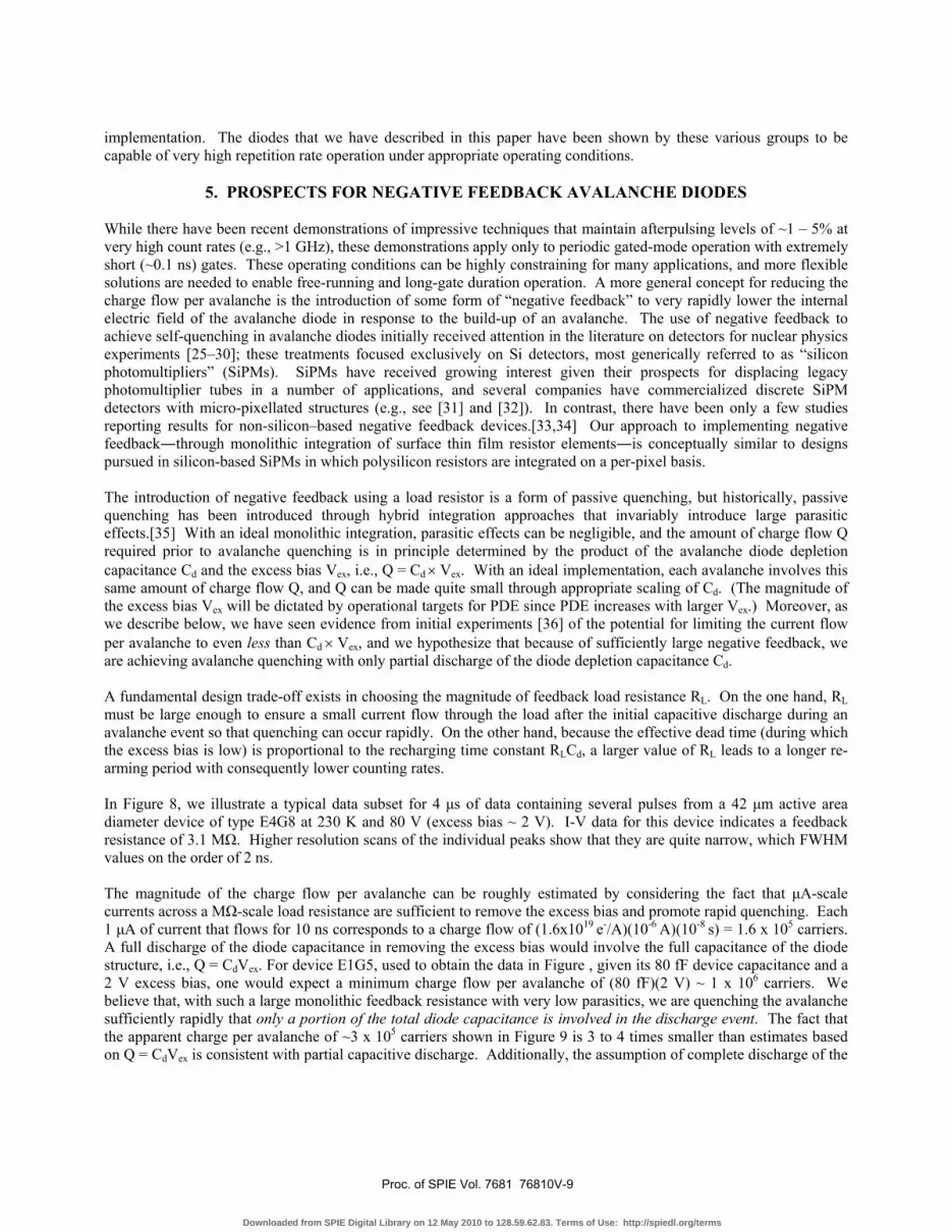
5. PROSPECTS FOR NEGATIVE FEEDBACK AVALANCHE DIODES While there have been recent demonstrations of impressive techniques that maintain afterpulsing levels of ~1 – 5% at very high count rates (e.g., >1 GHz), these demonstrations apply only to periodic gated-mode operation with extremely short (~0.1 ns) gates. These operating conditions can be highly constraining for many applications, and more flexible solutions are needed to enable free-running and long-gate duration operation. A more general concept for reducing the charge flow per avalanche is the introduction of some form of “negative feedback” to very rapidly lower the internal electric field of the avalanche diode in response to the build-up of an avalanche. The use of negative feedback to achieve self-quenching in avalanche diodes initially received attention in the literature on detectors for nuclear physics experiments [25–30]; these treatments focused exclusively on Si detectors, most generically referred to as “silicon photomultipliers” (SiPMs). SiPMs have received growing interest given their prospects for displacing legacy photomultiplier tubes in a number of applications, and several companies have commercialized discrete SiPM detectors with micro-pixellated structures (e.g., see [31] and [32]). In contrast, there have been only a few studies reporting results for non-silicon–based negative feedback devices.[33,34] Our approach to implementing negative feedback―through monolithic integration of surface thin film resistor elements―is conceptually similar to designs pursued in silicon-based SiPMs in which polysilicon resistors are integrated on a per-pixel basis. The introduction of negative feedback using a load resistor is a form of passive quenching, but historically, passive quenching has been introduced through hybrid integration approaches that invariably introduce large parasitic effects.[35] With an ideal monolithic integration, parasitic effects can be negligible, and the amount of charge flow Q required prior to avalanche quenching is in principle determined by the product of the avalanche diode depletion capacitance Cd and the excess bias Vex, i.e., Q = Cd × Vex. With an ideal implementation, each avalanche involves this same amount of charge flow Q, and Q can be made quite small through appropriate scaling of Cd. (The magnitude of the excess bias Vex will be dictated by operational targets for PDE since PDE increases with larger Vex.) Moreover, as we describe below, we have seen evidence from initial experiments [36] of the potential for limiting the current flow per avalanche to even less than Cd × Vex, and we hypothesize that because of sufficiently large negative feedback, we are achieving avalanche quenching with only partial discharge of the diode depletion capacitance Cd. A fundamental design trade-off exists in choosing the magnitude of feedback load resistance RL. On the one hand, RL must be large enough to ensure a small current flow through the load after the initial capacitive discharge during an avalanche event so that quenching can occur rapidly. On the other hand, because the effective dead time (during which the excess bias is low) is proportional to the recharging time constant RLCd, a larger value of RL leads to a longer re-arming period with consequently lower counting rates. In Figure 8, we illustrate a typical data subset for 4 μs of data containing several pulses from a 42 μm active area diameter device of type E4G8 at 230 K and 80 V (excess bias ~ 2 V). I-V data for this device indicates a feedback resistance of 3.1 MΩ. Higher resolution scans of the individual peaks show that they are quite narrow, which FWHM values on the order of 2 ns. The magnitude of the charge flow per avalanche can be roughly estimated by considering the fact that μA-scale currents across a MΩ-scale load resistance are sufficient to remove the excess bias and promote rapid quenching. Each 1 μA of current that flows for 10 ns corresponds to a charge flow of (1.6x10¹⁹ e-/A)(10-6 A)(10-8 s) = 1.6 x 10⁵ carriers. A full discharge of the diode capacitance in removing the excess bias would involve the full capacitance of the diode structure, i.e., Q = CdVex. For device E1G5, used to obtain the data in Figure , given its 80 fF device capacitance and a 2 V excess bias, one would expect a minimum charge flow per avalanche of (80 fF)(2 V) ~ 1 x 10⁶ carriers. We believe that, with such a large monolithic feedback resistance with very low parasitics, we are quenching the avalanche sufficiently rapidly that only a portion of the total diode capacitance is involved in the discharge event. The fact that the apparent charge per avalanche of ~3 x 10⁵ carriers shown in Figure 9 is 3 to 4 times smaller than estimates based on Q = CdVex is consistent with partial capacitive discharge. Additionally, the assumption of complete discharge of the
Proc. of SPIE Vol. 7681 76810V-9
Downloaded from SPIE Digital Library on 12 May 2010 to 128.59.62.83. Terms of Use: http://spiedl.org/terms
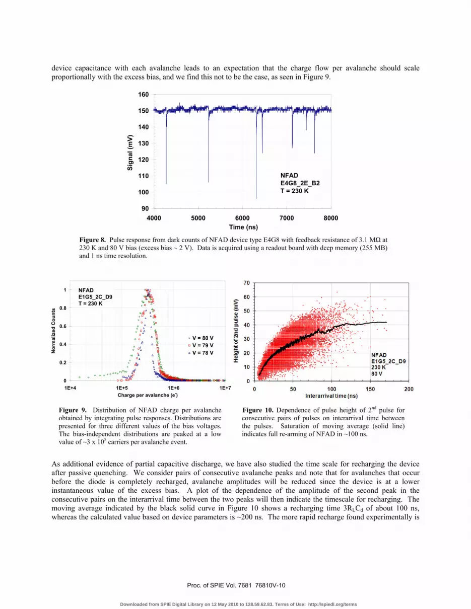
device capacitance with each avalanche leads to an expectation that the charge flow per avalanche should scale proportionally with the excess bias, and we find this not to be the case, as seen in Figure 9.
Figure 8. Pulse response from dark counts of NFAD device type E4G8 with feedback resistance of 3.1 MΩ at 230 K and 80 V bias (excess bias ~ 2 V). Data is acquired using a readout board with deep memory (255 MB) and 1 ns time resolution.
Figure 9. Distribution of NFAD charge per avalanche obtained by integrating pulse responses. Distributions are presented for three different values of the bias voltages. The bias-independent distributions are peaked at a low value of ~3 x 10⁵ carriers per avalanche event.
Figure 10. Dependence of pulse height of 2nd pulse for consecutive pairs of pulses on interarrival time between the pulses. Saturation of moving average (solid line) indicates full re-arming of NFAD in ~100 ns.
As additional evidence of partial capacitive discharge, we have also studied the time scale for recharging the device after passive quenching. We consider pairs of consecutive avalanche peaks and note that for avalanches that occur before the diode is completely recharged, avalanche amplitudes will be reduced since the device is at a lower instantaneous value of the excess bias. A plot of the dependence of the amplitude of the second peak in the consecutive pairs on the interarrival time between the two peaks will then indicate the timescale for recharging. The moving average indicated by the black solid curve in Figure 10 shows a recharging time 3RLCd of about 100 ns, whereas the calculated value based on device parameters is ~200 ns. The more rapid recharge found experimentally is
90
100
110
120
130
140
150
160
4000 5000 6000 7000 8000Time (ns)
Sign
al (m
V)
NFADE4G8_2E_B2T = 230 K
0
0.2
0.4
0.6
0.8
1
1E+4 1E+5 1E+6 1E+7Charge per avalanche (e-)
Nor
mal
ized
Cou
nts
V = 80 VV = 79 VV = 78 V
NFADE1G5_2C_D9T = 230 K
Proc. of SPIE Vol. 7681 76810V-10
Downloaded from SPIE Digital Library on 12 May 2010 to 128.59.62.83. Terms of Use: http://spiedl.org/terms

consistent with a smaller effective recharging capacitance associated with the initial partial discharge before quenching.
6. CONCLUSIONS Significant progress has been realized in fundamental SPAD performance such as the inherent tradeoff between DCR and PDE. We have described the main contributors to DCR through detailed modeling of the SPAD structure, and we have shown good agreement between the modeled temperature and bias dependence of the DCR activation energy and corresponding activation energy data obtained experimentally. Nothwithstanding this progress, however, high counting rates remain as a barrier to the use of SPADs in many photon counting applications. To surmount the present obstacles to higher counting repetition rate using SPADs, promising techniques based on novel backend electronic circuit designs have been introduced (including the self-differencing and sine-wave gating concepts). However, these concepts have so far been limited to periodic operation using very short gates. As an alternative path to high counting rates, we have introduced negative feedback to the conventional SPAD avalanche process to beneficially modify the device avalanche dynamics. The goal of this approach is to achieve consistent passive quenching with small carrier flow per avalanche by the monolithic integration of a suitable negative feedback element. We have demonstrated an implementation of this concept that leads to rather small avalanches (e.g., ~105 – 106 carriers), for which one expects reduced carrier trapping and an associated reduction in afterpulsing effects. We have also shown evidence that these negative feedback elements can induce avalanche quenching with only a partial discharge of the diode capacitance, holding out the prospect for even smaller avalanches and faster device re-arming than one would assume based on simple physical arguments.
ACKNOWLEDGMENTS We gratefully acknowledge Alberto Tosi, Franco Zappa, Massimo Ghioni, and Sergio Cova for insightful discussions, on-going collaboration, and especially for providing experimental data used in Figures 4 and 6. We are also grateful to Gary Smith for providing high temperature experimental data used to obtain results presented in Figure 6. Finally, we thank Bill Farr and Michael Krainak for valuable discussions concerning the NFAD concept and its characterization, and we acknowledge partial support for the NFAD work from JPL and NASA/GSFC.
REFERENCES [1] A. Lacaita, P. A. Francese, F. Zappa, and S. Cova, “Single-photon detection beyond 1 μm: performance of commercially
available InGaAs/InP detectors,” Appl. Opt., vol. 35, 2986 – 2996 (1996). [2] G. Ribordy, J. D. Gautier, H. Zbinden, and N. Gisin, “Performance of InGaAs/InP avalanche photodiodes as gated-mode photon
counters,” Appl. Opt., vol. 37, p. 2272–2277 (1998). [3] P. A. Hiskett, G. S. Buller, A. Y. Loudon, J. M. Smith, I. Gontijo, A. C. Walker, P. D. Townsend, and M. J. Robertson,
“Performance and design of InGaAs/InP photodiodes for single-photon counting at 1.55 μm,” Appl. Opt., vol. 39, p. 6818–6829 (2000).
[4] P. A. Hiskett, J. M. Smith, G. S. Buller, and P.D. Townsend, “Low-noise single-photon detection at wavelength 1.55 um,” Electron. Lett., vol. 37, p. 1081–1083 (2001).
[5] D. Stucki, G. Ribordy, A. Stefanov, H. Zbinden, J. G. Rarity, and T. Wall, “Photon counting for quantum key distribution with Peltier cooled InGaAs/InP APDs,” J. Modern Optics, vol. 48, no. 13, p. 1967–1981 (2001).
[6] M. A. Itzler, R. Ben-Michael, C.-F. Hsu, K. Slomkowski, A. Tosi, S. Cova, F. Zappa, and R. Ispasoiu, “Single photon avalanche diodes (SPADs) for 1.5 μm photon counting applications”, J. Mod. Opt., vol. 54, no. 2-3, p. 283–304, Feb. 2007
[7] K. Nishida, K. Taguchi, and Y. Matsumoto, “InGaAsP heterostructure avalanche photodiodes with high avalanche gain,” Appl. Phys. Lett., 35, p. 251–252 (1979).
[8] M. A. Itzler, K. K. Loi, S. McCoy, N. Codd, and N. Komaba, “High-performance, manufacturable avalanche photodiodes for 10 Gb/s optical receivers,” Proc. of 25th Optical Fiber Comm. Conf. (OFC 2000), 4, p. 126–128 (2000).
[9] R. J. McIntyre, “Multiplication noise in uniform avalanche diodes,” IEEE Trans. Electron Devices, vol. ED-13, no. 1, p. 164–168, Jul. 1973.
[10] R. J. McIntyre, “On the avalanche initiation probability of avalanche diodes above the breakdown voltage”, IEEE Trans. Electron Devices, vol. ED-20, no. 7, p. 637–641, Jul. 1973.
Proc. of SPIE Vol. 7681 76810V-11
Downloaded from SPIE Digital Library on 12 May 2010 to 128.59.62.83. Terms of Use: http://spiedl.org/terms

[11] F. Zappa, P. Lovati, and A. Lacaita, “Temperature dependence of electron and hole ionization coefficients in InP”, in Conf.
Proc. Int. Conf. indium phosphide and related materials (IPRM), Apr. 1996, p. 628–631. [12] X. Jiang, M. A. Itzler, R. Ben-Michael, K. Slomkowski, M. A. Krainak, S. Wu, and X. Sun, “Afterpulsing effects in free-
running InGaAsP single photon avalanche diodes,” IEEE J. Quantum Electron., vol. 44, p. 3–11 (2008). [13] J.P. Donnelly, E.K. Duerr, K.A. McIntosh, E.A. Dauler, D.C. Oakley, S.H. Groves, C.J. Vineis, L.J. Mahoney, K.M. Molvar,
P.I. Hopman, K.E. Jensen, G.M. Smith, S. Verghese, and D.C. Shaver, “Design considerations for 1.06-μm InGaAsP-InP Geiger-mode avalanche photodiodes”, IEEE J. Quantum Electron., vol. 42, no. 8, p. 797–809, Aug. 2006.
[14] X. Jiang, M. A. Itzler, R. Ben-Michael, and K. Slomkowski, “InGaAsP/InP avalanche photodiodes for single photon detection”, IEEE J. of Sel. Topics in Quantum Electronics 13, p. 895–905 (2007).
[15] The exponential expressions for α and β in [11 ] have a term containing tanh(E0/2kT) where E0 = 46 meV for α and E0 = 36 meV for β. This slight difference in the temperature variation of α and β gives rise to the local maximum in Ea(T) for low excess bias voltages.
[16] A. Tosi, A. Dalla Mora, F. Zappa, S. Cova, M.A. Itzler, X. Jiang, “InGaAs/InP Single-Photon Avalanche Diodes show low dark counts and require moderate cooling,” Proc. of SPIE 7222, 7222-1G (2010).
[17] R. Ben-Michael, M. A. Itzler, B. Nyman, and M. Entwistle, “Afterpulsing in InGaAs/InP single photon avalanche photodetectors”, 2006 Digest of the LEOS Summer Topical Meetings, p. 15–16 (2006).
[18] D.S. Bethune, W.P. Risk, and G.W. Pabst, “A high-performance integrated single-photon detector for telecom wavelengths”, J. Mod. Opt., vol. 51, no. 9–10, p. 1359–1368, June 2004.
[19] C. Hu, X. Zheng, J. C. Campbell, B. M. Onat, X. Jiang, and M. A. Itzler, “High-performance InGaAs/InP-based single photon avalanche diode with reduced afterpulsing,” Proc. of SPIE 7681, 7681-28 (2010).
[20] N. Namekata, S. Sasamori, and S. Inoue, Opt. Express, 14, 10043 (2006). [21] N. Namekata, S. Adachi, and S. Inoue, “Ultra-low-noise sinusoidally gated avalanche photodiode for high-speed single-photon
detection at telecommunication wavelengths,” Photonics Tech Lett. 22, p. 529 – 531 (2010). [22] J. Zhang, P. Eraerds, N. Walenta, C. Barreiro, R. Thew, and H. Zbinden, “2.23 GHz gating InGaAs/InP single-photon
avalanche diode for quantum key distribution,” Proc. of SPIE 7681, 7681-35 (2010). [23] Z.L. Yuan, B.E. Kardynal, A.W. Sharpe, and A.J. Shields, Appl. Phys. Lett. 91, 041114 (2007). [24] A. R. Dixon, J. F. Dynes, Z. L. Yuan, A. W. Sharpe, A. J. Bennett, and A. J. Shields, “Ultrashort dead time of photon-counting
InGaAs avalanche photodiodes,” Appl. Phys. Lett. 94, 231113 (2009). [25] D. Bisello, et al., Nuclear Instruments and Methods in Physics Research A 360, p. 83 – 86 (1995); ibid. 367, p. 212 – 214
(1995). [26] S. Afanasiev, et al., Nuclear Physics B 44, p. 402 – 405 (1995). [27] D. Shushakov and V. Shubin, Proc. of SPIE 2397, p. 544 – 554 (1995); V. Shubin and D. Shushakov, Proc. of SPIE 2415, p.
94 – 103 (1995). [28] D. Shushakov and V. Shubin, Proc. of SPIE 2699, p. 173 – 183 (1996). [29] G. Bondarenko, et al., Nucl. Phys. B 61B, p. 347 – 352 (1998). [30] P. Buzhan, et al., ICFA Instrumentation Bulletin (Fall 2001) [http://www.slac.stanford.edu/pubs/icfa/fall01.html] [31] http://sales.hamamatsu.com/en/products/solid-state-division/si-photodiode-series/mppc.php [32] http://sensl.com/products/silicon-photomultipliers/ [33] K. Zhao, A. Zhang, Y.-h. Lo, and W. Farr, Appl. Phys. Lett. 91, 081107 (2007); K. Zhao, S. You, J. Cheng, and Y.-h. Lo, Appl.
Phys. Lett. 93, 153504 (2008). [34] K. Linga, Y. Yevtukhov, and B. Liang, “Very high gain and low excess noise near infrared single photon avalanche detector: A
NIR solid state photomultiplier,” Proc. of SPIE 7320, 7320-0Z (2009). [35] S. Cova, M. Ghioni, A. Lacaita, C. Samori, and F. Zappa, Appl. Opt. 35, p. 1956 – 1976 (1996). [36] X. Jiang, M. A. Itzler, B. Nyman, and K. Slomkowski, “Negative Feedback Avalanche Diodes for Near-infrared Single Photon
Detection,” Proc. of SPIE 7320, 7320-11 (2009).
Proc. of SPIE Vol. 7681 76810V-12
Downloaded from SPIE Digital Library on 12 May 2010 to 128.59.62.83. Terms of Use: http://spiedl.org/terms


