Embed Size (px)
Citation preview
VISUALISATION OF LOCAL CHARGE DENSITIES
WITH
KELVIN PROBE FORCE MICROSCOPY
Dissertation
zur Erlangung des akademischen Grades
Doctor rerum naturalium(Dr. rer. nat.)
vorgelegt der
Fakultat Mathematik und NaturwissenschaftenTechnische Universitat Dresden
von
PETER MILDE
geboren am 9. Marz 1982 in Dresden
TECHNISCHE UNIVERSITAT DRESDEN 2011

1. Gutachter: Prof. L.M. Eng, Technische Universitat Dresden2. Gutachter: Prof. Chr. Loppacher, Universite Paul Cezanne, Marseille
Tag der Verteidigung: 10.06.2011


Contents
Abstract/Zusammenfassung ix
I Kelvin probe force microscopy 1
1 Introduction 31.1 Introduction . . . . . . . . . . . . . . . . . . . . . . . . . . . . . . . 3
1.1.1 The “contact electricity” of metals . . . . . . . . . . . . . . 31.1.2 Scanning probe microscopy . . . . . . . . . . . . . . . . . . 8
1.2 Kelvin probe force microscopy . . . . . . . . . . . . . . . . . . . . 111.2.1 Mathematical background . . . . . . . . . . . . . . . . . . . 111.2.2 Modes of operation . . . . . . . . . . . . . . . . . . . . . . . 141.2.3 General aspects of KPFM . . . . . . . . . . . . . . . . . . . 151.2.4 Application . . . . . . . . . . . . . . . . . . . . . . . . . . . 17
2 Origin of contrast in KPFM 192.1 Metal surfaces - initial contrast . . . . . . . . . . . . . . . . . . . . 19
2.1.1 Concept of a work function . . . . . . . . . . . . . . . . . . 192.1.2 The local vacuum level . . . . . . . . . . . . . . . . . . . . . 212.1.3 Implications for KPFM . . . . . . . . . . . . . . . . . . . . . 23
2.2 Metal/adsorbate-systems - adsorbate driven contrast . . . . . . . 252.2.1 Inorganic adsorbates . . . . . . . . . . . . . . . . . . . . . . 252.2.2 Organic adsorbates . . . . . . . . . . . . . . . . . . . . . . . 282.2.3 Implications for KPFM . . . . . . . . . . . . . . . . . . . . . 28
2.3 Insulating systems – polarisation induced contrast . . . . . . . . . 292.3.1 Free charge . . . . . . . . . . . . . . . . . . . . . . . . . . . 292.3.2 Free polarisation . . . . . . . . . . . . . . . . . . . . . . . . 302.3.3 Compound systems . . . . . . . . . . . . . . . . . . . . . . 32
2.4 Summary . . . . . . . . . . . . . . . . . . . . . . . . . . . . . . . . . 32
v

Contents
II Visualisation of Local Charge Densities 35
3 Experiment 37
4 Pristine metal surfaces 394.1 Au(111) - surface steps . . . . . . . . . . . . . . . . . . . . . . . . . 394.2 Au(111) - surface reconstruction I . . . . . . . . . . . . . . . . . . . 424.3 Au(111) - surface reconstruction II . . . . . . . . . . . . . . . . . . 464.4 Summary . . . . . . . . . . . . . . . . . . . . . . . . . . . . . . . . . 51
5 Metal/adsorbate-systems 535.1 Au(111)/dibutyl sexithiophene . . . . . . . . . . . . . . . . . . . . 535.2 Ag(111)/octachloro zinc phthalocyanine . . . . . . . . . . . . . . . 57
5.2.1 Phases P1 and P2 . . . . . . . . . . . . . . . . . . . . . . . . 595.2.2 Phases P3 and P4 . . . . . . . . . . . . . . . . . . . . . . . . 625.2.3 Disordered areas . . . . . . . . . . . . . . . . . . . . . . . . 665.2.4 Molecular resolution . . . . . . . . . . . . . . . . . . . . . . 67
5.3 Summary . . . . . . . . . . . . . . . . . . . . . . . . . . . . . . . . . 70
6 Ferroelectric materials 736.1 Lead zirconate titanate . . . . . . . . . . . . . . . . . . . . . . . . . 736.2 Initial contact potential contrast . . . . . . . . . . . . . . . . . . . . 766.3 Induced contact potential contrast . . . . . . . . . . . . . . . . . . 806.4 Summary . . . . . . . . . . . . . . . . . . . . . . . . . . . . . . . . . 85
7 Ferroelectric/organic-systems 877.1 Lead zirconate titanate/cyano butyl phosphonic acid butyl thio-
phene . . . . . . . . . . . . . . . . . . . . . . . . . . . . . . . . . . . 887.2 Lead zirconate titanate/dicyano dibutylquaterthiophene . . . . . 937.3 Summary . . . . . . . . . . . . . . . . . . . . . . . . . . . . . . . . . 97
8 Conclusion 998.1 Synopsis . . . . . . . . . . . . . . . . . . . . . . . . . . . . . . . . . 998.2 Prospects . . . . . . . . . . . . . . . . . . . . . . . . . . . . . . . . . 101
8.2.1 3D-spectroscopy . . . . . . . . . . . . . . . . . . . . . . . . 1018.2.2 Stroboscopic Kelvin probe force microscopy . . . . . . . . 103
8.3 Closing remarks . . . . . . . . . . . . . . . . . . . . . . . . . . . . . 106
vi

Contents
III Appendix 107
A Piezoresponse force microscopy 109
B Kelvin application note 111
C Calculation with model charge densities 117
D Picture gallery 119
Bibliography I
Acknowledgement XIX
Abbreviations and Symbols XXI
vii

Abstract/Zusammenfassung
For the past decades, Kelvin probe force microscopy (KPFM) developed from asidebranch of atomic force microscopy to a widely used standard technique. Itallows to measure electrostatic potentials on any type of sample material with anunprecedented spatial resolution. While the technical aspects of the method arewell understood, the interpretation of measured data remains object of intenseresearch. This thesis intends to prove an advanced view on how sample sys-tems which are typical for ultrahigh resolution imaging, such as organic molec-ular submonolayers on metals, can be quantitavily analysed with the differentialcharge density model.
In the first part a brief introduction into the Kelvin probe experiment andatomic force microscopy is given. A short review of the theoretical backgroundof the technique is presented.
Following, the differential charge density model is introduced, which is usedto further explain the origin of contrast in Kelvin probe force microscopy. Phys-ical effects, which cause the occurence of local differential charge densities, arereviewed for several sample systems that are of interest in high resolution atomicforce microscopy.
Experimental evidence for these effects is presented in the second part. Atomicforce microscopy was used for in situ studies of a variety of sample systems rang-ing from pristine metal surfaces over monolayer organic adsorbates on metals toferroelectric substrates both, with and without organic thin film coverage.
As the result from these studies, it is shown that the differential charge den-sity model accurately describes the experimentally observed potential contrasts.This implies an inherent disparity of the measurement results between the differ-ent Kelvin probe force microscopy techniques; a point which had been overseenso far in the discussion of experimental data. Especially for the case of laterallystrong confined differential charge densities, the results show the opportunityas well as the necessity to explain experimental data with a combination of abinitio calculations of the differential charge density and an electrostatic model ofthe tip-sample interaction.
ix
Abstract/Zusammenfassung
In den vergangenen Jahrzehnten hat sich die Kelvinrasterkraftmikroskopievon einer ausgefallenen Unterart der Rasterkraftmikroskopie zu einer viel-seitig eingesetzten Standardtechnik entwickelt. Sie erlaubt unabhangig vomMaterial der untersuchten Probe die Vermessung elektrostatischer Potentialemit unubertroffener raumlicher Auflosung. Wahrend die technischen As-pekte der Methode weitestgehend verstanden sind, verbleibt die Interpreta-tion gemessener Daten Gegenstand intensiver Forschung. Diese Arbeit un-tersucht die Anwendung des Modells der Differenzladungsdichte auf die furhochauflosende Rasterkraftmikroskopie typischen Probensysteme, wie zumBeispiel Submonolagen organischer Molekule auf Metallen.
Im ersten Teil wird nach einer Einfuhrung in das Kelvinexperiment und dieRasterkraftmikroskopie ein Uberblick uber die theoretischen Grundlagen der ex-perimentellen Techniken prasentiert.
Folgend wird das Modell der Differenzladungsdichte, welches im weit-eren dazu benutzt wird den Ursprung des Bildkontrastes in der Kelvinkraft-mikroskopie zu erklaren, vorgestellt. Physikalische Effekte, die lokale Differen-zladungsdichten hervorrufen, werden fur die fur hochauflosende Rasterkraft-mikroskopie typischen Probensysteme erortert.
Der experimentelle Nachweis solcher Effekte wird im zweiten Teil erbracht.Rasterkraftmikroskopie wurde fur in situ Untersuchungen einer Reihe vonProbensystemen genutzt, welche von einfachen metallischen Oberflachen uberMetalle mit Monolagen organischen Adsorbates bis hin zu ferroelektrischenSubstraten, sowohl mit als auch ohne Bedeckung organischer Dunnschichten,reichen.
Als Ergebnis dieser Untersuchungen wird gezeigt, dass das Modell derDifferenzladungsdichte die im Experiment beobachteten Potentialkontrasteakkurat beschreibt. Daraus folgt eine implizite Ungleichheit zwischenden Messergebnissen der unterschiedlichen Kelvinkraftmikroskopiemethoden;ein Fakt dem bisher wenig Beachtung bei der Auswertung von experi-mentellen Ergebnissen entgegengebracht wurde. Besonders fur lateral starkbeschrankte Objekte ergibt sich daraus die Moglichkeit und Notwendigkeitexperimentelle Daten mit einer Kombination aus ab initio Kalkulation derDifferenzladungsdichte und elektrostatischer Modellierung des Probe-Spitze-Systems zu beschreiben.
x
Part I
Kelvin probe force microscopy


1 Introduction
If at first, the idea is not absurd, then there is no hopefor it.Albert Einstein
1.1 Introduction
1.1.1 The “contact electricity” of metals
Volta’s discovery
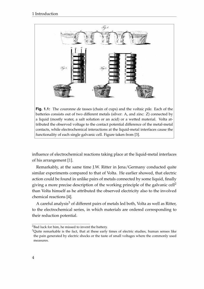
At the beginning of the 19th century, the invention of the voltaic pile (see figure1.1) by Allesandro Volta [1] opened up a whole new space of experimentalpossibilities in the field of electricity [2]. This development was the result ofa controversy between Volta and the galvanists about the interpretation of thefamous frog experiment of Luigi Galvani. The galvanists believed in a kind ofelectricity inherent to biological tissue, which would cause the reaction of thedead frog when metallic contact was made between the two ends of a leg. Incontrary, Volta saw the reason for this reaction in the metal contact itself, sincethe experiment worked best, if at least one pair of metals in series was used toestablish the contact.
This observation led him to experiments with metal pairs and the discoveryof a “contact electricity”, which in modern language is the same as the contactpotential difference (CPD) originating in a work function difference of the twoinvolved materials. As a result of his experiments and in order to show that thegalvanists were wrong, he constructed the voltaic pile - the first battery ever. Hebelieved to disprove the ideas of galvanism, since no biological tissue was neces-sary to produce electricity. Consequently, Volta argued for the contact electricityas the only origin of the electric action1 observed on the open pile and denied the
1The terms current and voltage were not clearly formulated at this time.
3
1 Introduction
Fig. 1.1: The couronne de tasses (chain of cups) and the voltaic pile. Each of thebatteries consists out of two different metals (silver: A, and zinc: Z) connected bya liquid (mostly water, a salt solution or an acid) or a wetted material. Volta at-tributed the observed voltage to the contact potential difference of the metal-metalcontacts, while electrochemical interactions at the liquid-metal interfaces cause thefunctionality of each single galvanic cell. Figure taken from [3].
influence of electrochemical reactions taking place at the liquid-metal interfacesof his arrangement [1].
Remarkably, at the same time J.W. Ritter in Jena/Germany conducted quitesimilar experiments compared to that of Volta. He earlier showed, that electricaction could be found in unlike pairs of metals connected by some liquid, finallygiving a more precise description of the working principle of the galvanic cell2
than Volta himself as he attributed the observed electricity also to the involvedchemical reactions [4].
A careful analysis3 of different pairs of metals led both, Volta as well as Ritter,to the electrochemical series, in which materials are ordered corresponding totheir reduction potential.
2Bad luck for him, he missed to invent the battery.3Quite remarkable is the fact, that at these early times of electric studies, human senses likethe pain generated by electric shocks or the taste of small voltages where the commonly usedmeasures.
4
1.1 Introduction
The experiment of Lord Kelvin
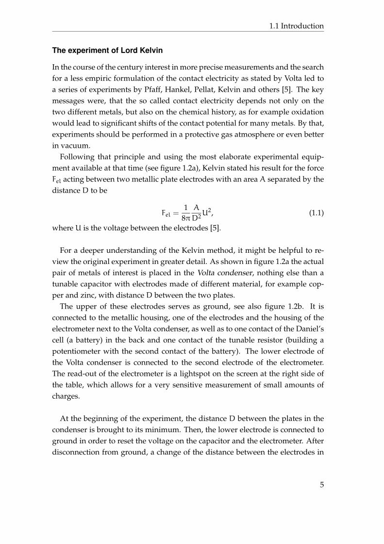
In the course of the century interest in more precise measurements and the searchfor a less empiric formulation of the contact electricity as stated by Volta led toa series of experiments by Pfaff, Hankel, Pellat, Kelvin and others [5]. The keymessages were, that the so called contact electricity depends not only on thetwo different metals, but also on the chemical history, as for example oxidationwould lead to significant shifts of the contact potential for many metals. By that,experiments should be performed in a protective gas atmosphere or even betterin vacuum.
Following that principle and using the most elaborate experimental equip-ment available at that time (see figure 1.2a), Kelvin stated his result for the forceFel acting between two metallic plate electrodes with an area A separated by thedistance D to be
Fel =1
8πA
D2U2, (1.1)
where U is the voltage between the electrodes [5].
For a deeper understanding of the Kelvin method, it might be helpful to re-view the original experiment in greater detail. As shown in figure 1.2a the actualpair of metals of interest is placed in the Volta condenser, nothing else than atunable capacitor with electrodes made of different material, for example cop-per and zinc, with distance D between the two plates.
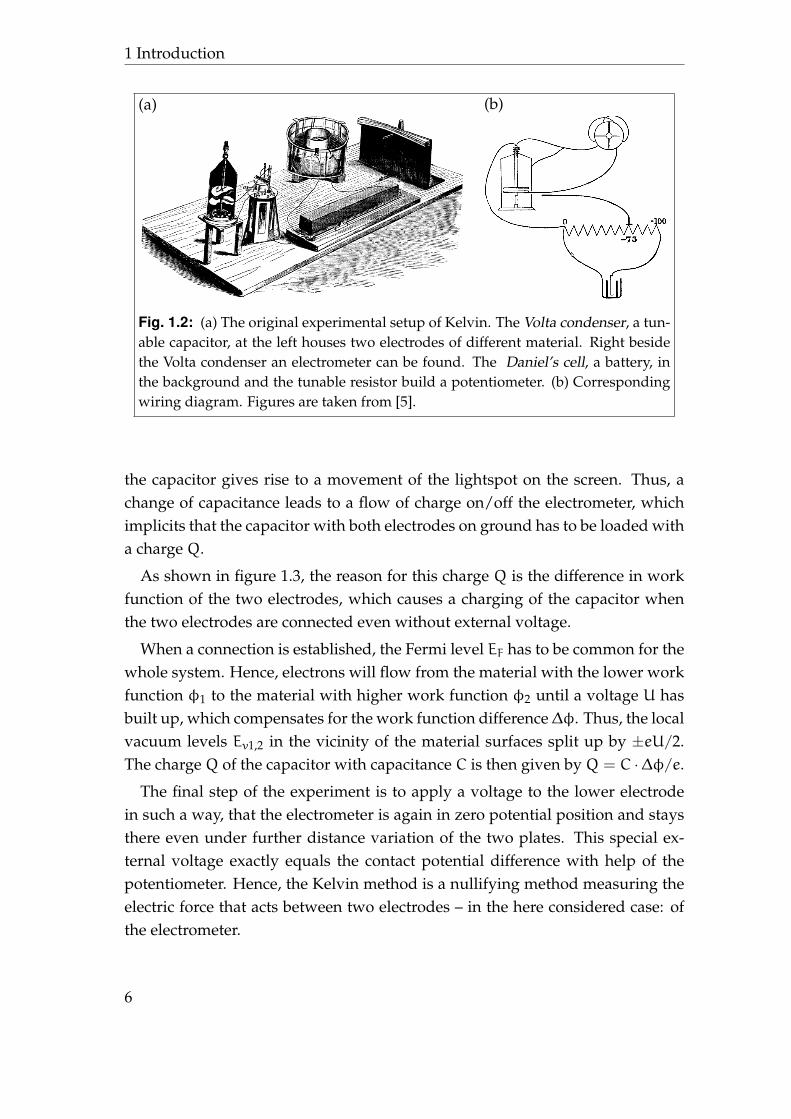
The upper of these electrodes serves as ground, see also figure 1.2b. It isconnected to the metallic housing, one of the electrodes and the housing of theelectrometer next to the Volta condenser, as well as to one contact of the Daniel’scell (a battery) in the back and one contact of the tunable resistor (building apotentiometer with the second contact of the battery). The lower electrode ofthe Volta condenser is connected to the second electrode of the electrometer.The read-out of the electrometer is a lightspot on the screen at the right side ofthe table, which allows for a very sensitive measurement of small amounts ofcharges.
At the beginning of the experiment, the distance D between the plates in thecondenser is brought to its minimum. Then, the lower electrode is connected toground in order to reset the voltage on the capacitor and the electrometer. Afterdisconnection from ground, a change of the distance between the electrodes in
5
1 Introduction
(a) (b)
Fig. 1.2: (a) The original experimental setup of Kelvin. The Volta condenser, a tun-able capacitor, at the left houses two electrodes of different material. Right besidethe Volta condenser an electrometer can be found. The Daniel’s cell, a battery, inthe background and the tunable resistor build a potentiometer. (b) Correspondingwiring diagram. Figures are taken from [5].
the capacitor gives rise to a movement of the lightspot on the screen. Thus, achange of capacitance leads to a flow of charge on/off the electrometer, whichimplicits that the capacitor with both electrodes on ground has to be loaded witha charge Q.
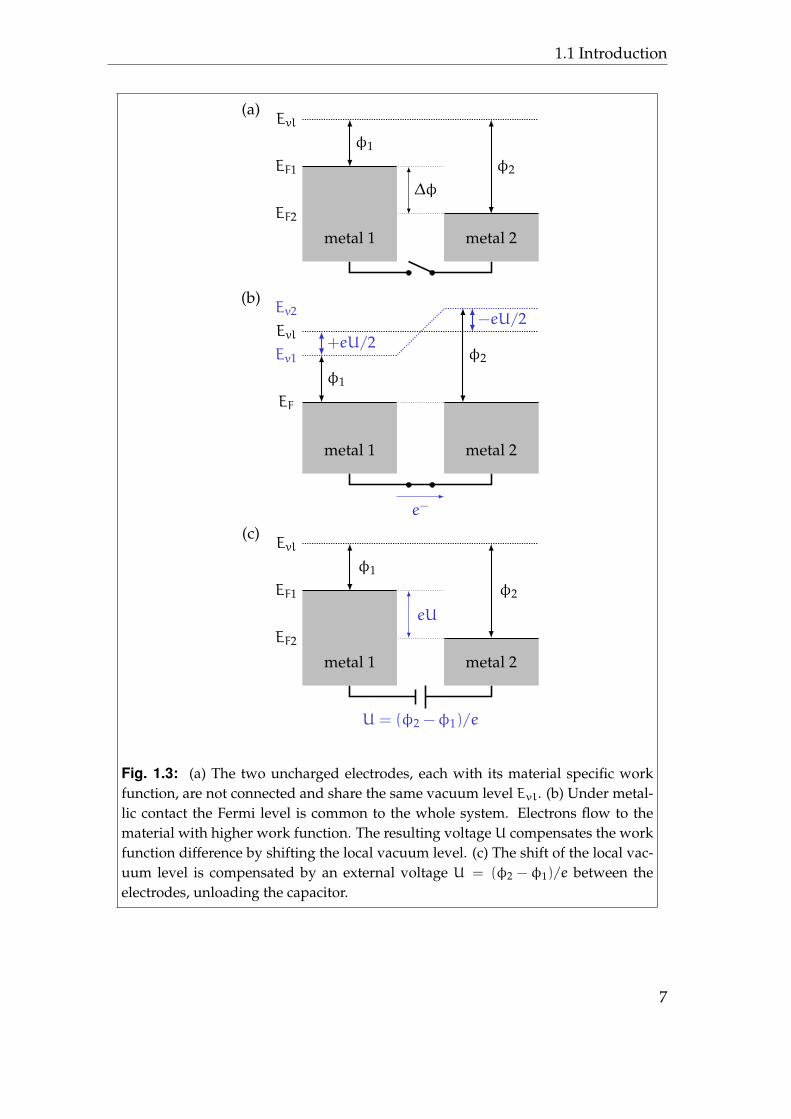
As shown in figure 1.3, the reason for this charge Q is the difference in workfunction of the two electrodes, which causes a charging of the capacitor whenthe two electrodes are connected even without external voltage.
When a connection is established, the Fermi level EF has to be common for thewhole system. Hence, electrons will flow from the material with the lower workfunction φ1 to the material with higher work function φ2 until a voltage U hasbuilt up, which compensates for the work function difference∆φ. Thus, the localvacuum levels Ev1,2 in the vicinity of the material surfaces split up by ±eU/2.The chargeQ of the capacitor with capacitance C is then given byQ = C ·∆φ/e.
The final step of the experiment is to apply a voltage to the lower electrodein such a way, that the electrometer is again in zero potential position and staysthere even under further distance variation of the two plates. This special ex-ternal voltage exactly equals the contact potential difference with help of thepotentiometer. Hence, the Kelvin method is a nullifying method measuring theelectric force that acts between two electrodes – in the here considered case: ofthe electrometer.
6
1.1 Introduction
(a)Evl
EF1
EF2
∆φ
φ1
metal 1
φ2
metal 2
(b)
Evl
Ev1
Ev2
e−
EF
φ1
+eU/2
metal 1
φ2
−eU/2
metal 2
(c)Evl
EF1
EF2
U = (φ2 −φ1)/e
eU
φ1
metal 1
φ2
metal 2
Fig. 1.3: (a) The two uncharged electrodes, each with its material specific workfunction, are not connected and share the same vacuum level Evl. (b) Under metal-lic contact the Fermi level is common to the whole system. Electrons flow to thematerial with higher work function. The resulting voltage U compensates the workfunction difference by shifting the local vacuum level. (c) The shift of the local vac-uum level is compensated by an external voltage U = (φ2 − φ1)/e between theelectrodes, unloading the capacitor.
7
1 Introduction
Nowadays, a very elegant way to measure even smallest forces is the atomicforce microscope (AFM) invented in 1986 by Binnig, Quate and Gerber [6]. It is amember of the family of scanning probe microscopes, of which the non-contactatomic force microscope (nc-AFM) will be introduced in the following.
1.1.2 Scanning probe microscopy
General aspects
Interactions in physics are typically described with help of interaction fields, forexample force fields, which describe the interaction of an object (the sample)with a “testing”-object (the probe). The only conditions for the test-object areto take part in the interaction without giving change to it and to be small com-pared to the typical variation length of the interaction field. Further, interactionfields are a function of relative position to the object. A scanning probe micro-scope, whatever interaction and direct or indirect detection method it is basedon, translates this model into an experimental technique.
The beginning of the scanning probe microscopy era was the invention of thescanning tunnelling microscope (STM) by Gerd Binnig and Heinrich Rohrer in1982 [7]. A few years later, in 1986, Binnig, Quate and Gerber [6] constructedthe first atomic force microscope. After that the family of scanning probe mi-croscopy methods started to grow. Today more than 30 more or less differenttechniques are known , each probing a specific type of interaction4. Also com-mon to all scanning probe methods is the rather strong influence of the probe.This is mostly due to the fact, that it is nearly impossible to build a probe whichis smaller than the variation length of the interaction. For the interpretation ofrecorded images a comprehensive knowledge of the probe properties is oblig-atory, but often not obtainable. Hence, the biggest drawback of any scanningprobe microscopy is its beauty, namely the use of a probe to achieve a real spaceimage of a physical property.
Non-contact atomic force microscopy
One rather wide applicable scanning probe technique is the non-contact atomicforce microscopy introduced by Albrecht in 1991 [8] based on the dynamic AFMdeveloped by Martin, Williams and Wickramasinghe [9] and further improvedby introduction of the phase-locked loop technique [10, 11]. The basic idea is to
4Quite often equal information can be obtained by different detection schemes.
8
1.1 Introduction
use an oscillating mass spring system in order to detect forces acting betweenthe sample and the test mass. The spring consists of a micro fabricated can-tilever which is rigidly connected to a shaker piezo at one side. The test massitself is a small tip which is mounted at the free end of the cantilever. The funda-mental eigenfrequencies of such cantilevers vary typically between 13 kHz and3 MHz. For separation control the fundamental eigenfrequency is used, whilehigher eigenfrequencies [12] can be used to obtain additional sample informa-tion [13, 14]. Naturally, non-conservative forces will then lead to a higher dis-sipation of the kinetic energy. Conservative forces on the one hand provoke ashift of the equilibrium position and on the other hand a shift of the cantileverseigenfrequencies.
The system can be described by a sum of driven harmonic oscillators i (i ∈ N)which are free to move in z-direction with eigenfrequenciesωi, spring constantski and quality factors5 Qi which are disturbed by an external, conservative forcefield ~Fts(~r) [15]. Dissipative forces and their spatial variation are absorbed in thequality factors Qi. For each of these oscillators the equation of motion reads
z+ωiQiz+ω2
i z =ω2i
ki{Fts,z(z) +Aexc · cos(ωt)} , (1.2)
under negligence of lateral force components6. In order to illustrate the effect ofthe tip-sample forces, they might be expanded in a Taylor-series in z around theequilibrium position z0
z+ωiQiz+ω2
i z =ω2i
ki
{Fts,z(z0) +
∂Fts,z(z0)
∂z· z+ . . . +Aexc · cos(ωt)
}. (1.3)
While the static term defines the equilibrium position z0, the gradient of theforce acts as a second spring constant and leads to a resonance frequency
ωres,i = ωi
√1 −
1ki
∂Fts,z(z0)
∂z(1.4)
≈ ωi
{1 −
12ki
∂Fts,z(z0)
∂z
}. (1.5)
5With the damping time constant τi, the given approximation is valid for τi ·ωi � 1, thus forhigh quality factors Qi.
6Lateral forces lead to constant tilting (x-component) and buckling (y-component) of the can-tilever. Only if the derivatives ∂Fts,x
∂z and ∂Fts,y∂z are in the same order of magnitude as ∂Fts,z
∂z
corrections to the used simplification have to be taken into account.
9
1 Introduction
A more general treatment of the problem is given by Giessibl [16]. For non-linear force-distance laws the frequency shift ∆ωi = ωres,i −ωi is a weightedaverage of the force over a full oscillation cycle
∆ωi = −ωiπkiA
∫π0
dξ Fts,z(z0 +A cos(ξ)) · cos(ξ) (1.6)
with amplitude A. In practice, excitation frequencies either are eigenfrequenciesor lie far below the fundamental eigenfrequency ω0. The motion of the i-th os-cillator is to first order7 sinusoidal with Amplitude Ai and phase ϕi. In total allcontributions sum up to a single driven oscillation:
z = z0 +Aexc
∞∑i=0
Qiωres,ikiω
[1 +
1tan2(−ϕi)
]− 12
cos(ωt+ϕi) (1.7)
ϕi = − arctan
ω ·ωres,iQi
(ω2res,i −ω
2) . (1.8)
In order to study the force interaction between tip and sample, the cantileveris driven at its fundamental resonance ωres,0 and the shift of the resonancefrequency is measured relative to the undisturbed oscillation far away from thesample. To maintain the resonance condition ϕ0 = −π/2, a phase-locked loop[10, 11] is used, which adjusts the excitation frequency ω to the present reso-nance frequencyωres,0. For stable image acquisition, additionally the oscillationamplitude A has to be kept fix . Changes in the excitation amplitude Aexc arethen related to dissipative forces. Images are obtained in either constant height8
or constant frequency shift9 mode.
Among all interaction forces, capacitive force are always present for electri-cally conductive tips. These are of same origin as in the experiment of Kelvindescribed in section 1.1.1. Furthermore, the non-contact atomic force microscoperesembles Kelvins experimental setup: two conductive electrodes of in generaldifferent material, a variable distance between the electrodes and a measure of
7Higher harmonics of the drive frequency ω can occur for highly non-linear force-distance lawsand low-Q cantilevers.
8A real space plane z = z0 +m · x+n · y is scanned and the frequency shift is recorded.9The distance between tip and sample is adjusted such, that the frequency shift between theundisturbed oscillation far away from the sample and the disturbed oscillation near to the sam-ple is kept constant during the scan. z(x,y|∆ω = const.) is recorded as image.
10
1.2 Kelvin probe force microscopy
the acting electrostatic force. The only differences are first, that there is no phys-ical separation between tunable capacitor and force measurement, and second,that forces are measured in a dynamic rather than a static way. In consequencethe measurement of contact potential differences with non-contact atomic forcemicroscopy is named Kelvin probe force microscopy [17], which will be furtherintroduced in the following section.
1.2 Kelvin probe force microscopy
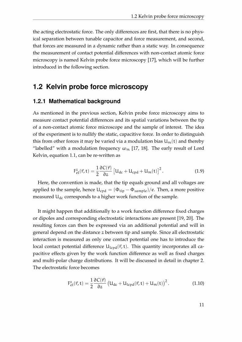
1.2.1 Mathematical background
As mentioned in the previous section, Kelvin probe force microscopy aims tomeasure contact potential differences and its spatial variations between the tipof a non-contact atomic force microscope and the sample of interest. The ideaof the experiment is to nullify the static, capacitive force. In order to distinguishthis from other forces it may be varied via a modulation bias Um(t) and thereby“labelled” with a modulation frequency ωm [17, 18]. The early result of LordKelvin, equation 1.1, can be re-written as
Fzel(~r, t) =12∂C(~r)
∂z
[Udc +Ucpd +Um(t)
]2 . (1.9)
Here, the convention is made, that the tip equals ground and all voltages areapplied to the sample, hence Ucpd = (Φtip −Φsample)/e. Then, a more positivemeasured Udc corresponds to a higher work function of the sample.
It might happen that additionally to a work function difference fixed chargesor dipoles and corresponding electrostatic interactions are present [19, 20]. Theresulting forces can then be expressed via an additional potential and will ingeneral depend on the distance z between tip and sample. Since all electrostaticinteraction is measured as only one contact potential one has to introduce thelocal contact potential difference Ulcpd(~r, t). This quantity incorporates all ca-pacitive effects given by the work function difference as well as fixed chargesand multi-polar charge distributions. It will be discussed in detail in chapter 2.The electrostatic force becomes
Fzel(~r, t) =12∂C(~r)
∂z
(Udc +Ulcpd(~r, t) +Um(t)
)2 . (1.10)
11
1 Introduction
In general, the local contact potential difference might be time dependent, forexample if the origin has to be found in non-localized free charges [21, 22] orphoto-induced excitations. In the following, this time dependence is thoughtto be very slow with respect to the typical measurement time, especially muchslower than the applied modulation bias frequency ωm and the fundamentaleigenfrequency ω0 of the cantilever10. Furthermore, the local contact potentialdifference as well as the capacitance gradient can depend on both lateral posi-tion (x,y) and distance z between tip and sample [20, 23].With a sinusoidal modulation bias Um(t) = um · cos(ωmt) equation (1.10) be-comes 11
Fzel(~r, t) = Fstat.el (~r, t) + Fωmel (~r, t) + F2ωmel (~r, t)
=12∂C(~r)
∂z·[{Udc +Ulcpd(~r)
}2+u2m
2
]+
+∂C(~r)
∂z·{Udc +Ulcpd(~r)
}· um · cos(ωmt) +
+14∂C(~r)
∂z· u2m · sin(2ωmt). (1.11)
Effectively, such an electrostatic force causes a shift of the cantilevers equilib-rium position. The overall force is an average over a full oscillation cycle:
∆z0 =12· I0(~r) ·
∞∑i=0
1ki
ω2i
ω2res,i
(1.12)
I0(~r) =1π
∫π0
dξ∂C(~r)
∂z·[{Udc +Ulcpd(~r)
}2+u2m
2
]. (1.13)
The time dependent components of the electrostatic force lead to driven oscil-lations with amplitude Aωm and A2ωm after equation 1.7 given by
zωm = I1(~r) · um∞∑i=0
Qiωres,ikiωm
[1 +
1tan2(−ϕi)
]− 12
cos(ωmt+ϕi) (1.14)
10Hereafter, the explicit time dependence is omitted in all calculations. Comments on experi-ments probing effects which are beyond the intrinsic bandwidth of FM-AFM will be given in8.2.
11The superscript “static” denotes that Fstat.el (~r, t) does not depend on the modulation frequencyωm, while it can still be time dependent in the above mentioned sense.
12
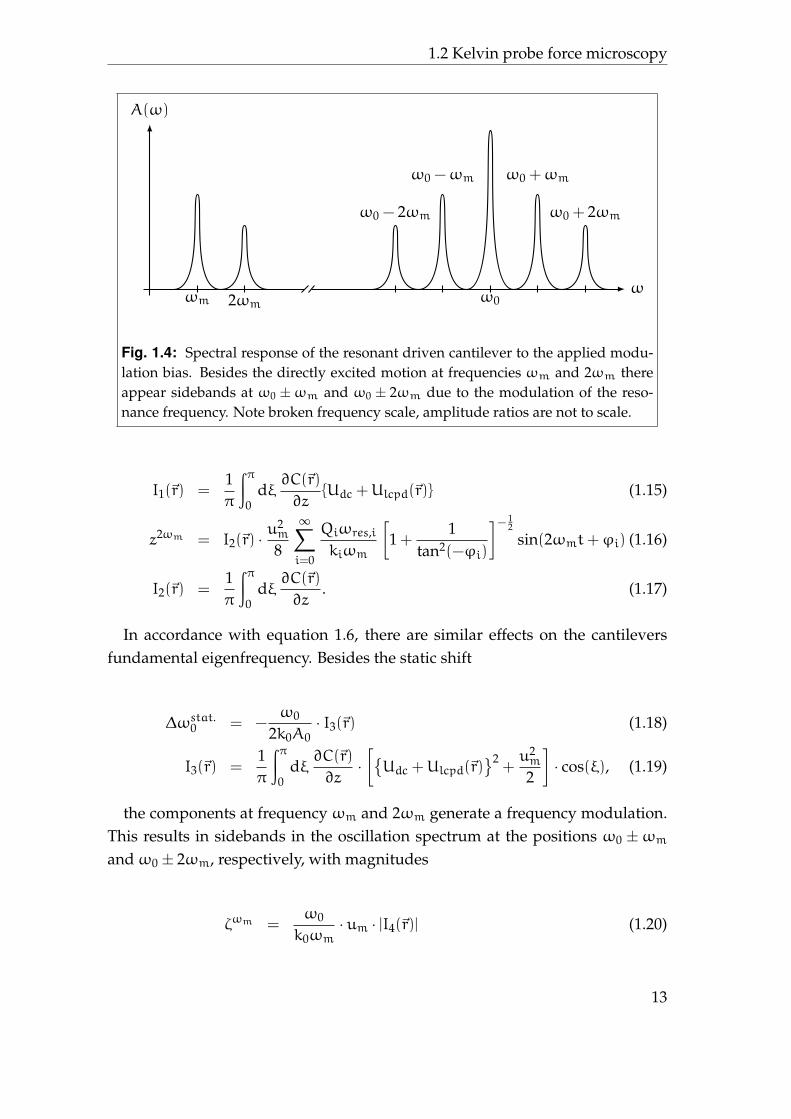
1.2 Kelvin probe force microscopy
ω
A(ω)
ωm 2ωm
ω0 − 2ωm
ω0 −ωm
ω0
ω0 +ωm
ω0 + 2ωm
Fig. 1.4: Spectral response of the resonant driven cantilever to the applied modu-lation bias. Besides the directly excited motion at frequencies ωm and 2ωm thereappear sidebands at ω0 ±ωm and ω0 ± 2ωm due to the modulation of the reso-nance frequency. Note broken frequency scale, amplitude ratios are not to scale.
I1(~r) =1π
∫π0
dξ∂C(~r)
∂z{Udc +Ulcpd(~r)} (1.15)
z2ωm = I2(~r) ·u2m
8
∞∑i=0
Qiωres,ikiωm
[1 +
1tan2(−ϕi)
]− 12
sin(2ωmt+ϕi) (1.16)
I2(~r) =1π
∫π0
dξ∂C(~r)
∂z. (1.17)
In accordance with equation 1.6, there are similar effects on the cantileversfundamental eigenfrequency. Besides the static shift
∆ωstat.0 = −ω0
2k0A0· I3(~r) (1.18)
I3(~r) =1π
∫π0
dξ∂C(~r)
∂z·[{Udc +Ulcpd(~r)
}2+u2m
2
]· cos(ξ), (1.19)
the components at frequency ωm and 2ωm generate a frequency modulation.This results in sidebands in the oscillation spectrum at the positions ω0 ±ωmandω0 ± 2ωm, respectively, with magnitudes
ζωm =ω0
k0ωm· um · |I4(~r)| (1.20)
13
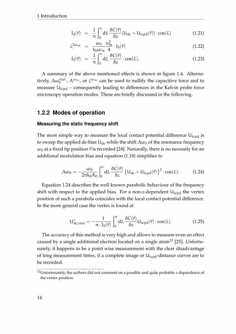
1 Introduction
I4(~r) =1π
∫π0
dξ∂C(~r)
∂z{Udc +Ulcpd(~r)} · cos(ξ) (1.21)
ζ2ωm =ω0
k0ωm
u2m
4· I5(~r) (1.22)
I5(~r) =1π
∫π0
dξ∂C(~r)
∂z· cos(ξ). (1.23)
A summary of the above mentioned effects is shown in figure 1.4. Alterna-tively, ∆ωstat.0 , Aωm , or ζωm can be used to nullify the capacitive force and tomeasure Ulcpd – consequently leading to differences in the Kelvin probe forcemicroscopy operation modes. These are briefly discussed in the following.
1.2.2 Modes of operation
Measuring the static frequency shift
The most simple way to measure the local contact potential difference Ulcpd isto sweep the applied dc-bias Udc while the shift ∆ω0 of the resonance frequencyω0 at a fixed tip position~r is recorded [24]. Naturally, there is no necessity for anadditional modulation bias and equation (1.18) simplifies to
∆ω0 = −ω0
2πk0A0
∫π0
dξ∂C(~r)
∂z
{Udc +Ulcpd(~r)
}2 · cos(ξ). (1.24)
Equation 1.24 describes the well known parabolic behaviour of the frequencyshift with respect to the applied bias. For a non-z-dependent Ulcpd the vertexposition of such a parabola coincides with the local contact potential difference.In the more general case the vertex is found at
U∗dc,stat = −1
π · I5(~r)
∫π0
dξ∂C(~r)
∂zUlcpd(~r) · cos(ξ). (1.25)
The accuracy of this method is very high and allows to measure even an effectcaused by a single additional electron located on a single atom12 [25]. Unfortu-nately, it happens to be a point wise measurement with the clear disadvantageof long measurement times, if a complete image or Ulcpd-distance curves are tobe recorded.
12Unfortunately, the authors did not comment on a possible and quite probable z-dependence ofthe vertex position.
14
1.2 Kelvin probe force microscopy
Amplitude de-modulation methods
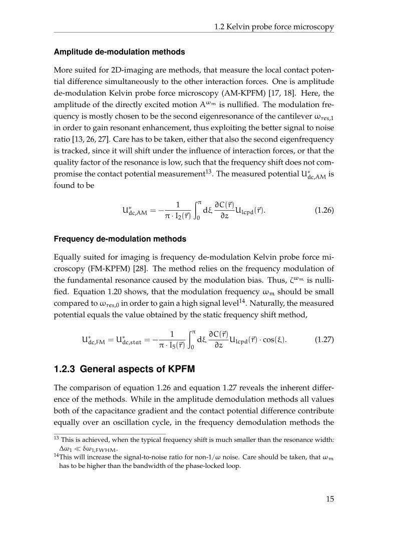
More suited for 2D-imaging are methods, that measure the local contact poten-tial difference simultaneously to the other interaction forces. One is amplitudede-modulation Kelvin probe force microscopy (AM-KPFM) [17, 18]. Here, theamplitude of the directly excited motion Aωm is nullified. The modulation fre-quency is mostly chosen to be the second eigenresonance of the cantileverωres,1in order to gain resonant enhancement, thus exploiting the better signal to noiseratio [13, 26, 27]. Care has to be taken, either that also the second eigenfrequencyis tracked, since it will shift under the influence of interaction forces, or that thequality factor of the resonance is low, such that the frequency shift does not com-promise the contact potential measurement13. The measured potential U∗dc,AM isfound to be
U∗dc,AM = −1
π · I2(~r)
∫π0
dξ∂C(~r)
∂zUlcpd(~r). (1.26)
Frequency de-modulation methods
Equally suited for imaging is frequency de-modulation Kelvin probe force mi-croscopy (FM-KPFM) [28]. The method relies on the frequency modulation ofthe fundamental resonance caused by the modulation bias. Thus, ζωm is nulli-fied. Equation 1.20 shows, that the modulation frequency ωm should be smallcompared toωres,0 in order to gain a high signal level14. Naturally, the measuredpotential equals the value obtained by the static frequency shift method,
U∗dc,FM = U∗dc,stat = −1
π · I5(~r)
∫π0
dξ∂C(~r)
∂zUlcpd(~r) · cos(ξ). (1.27)
1.2.3 General aspects of KPFM
The comparison of equation 1.26 and equation 1.27 reveals the inherent differ-ence of the methods. While in the amplitude demodulation methods all valuesboth of the capacitance gradient and the contact potential difference contributeequally over an oscillation cycle, in the frequency demodulation methods the
13 This is achieved, when the typical frequency shift is much smaller than the resonance width:∆ω1 � δω1,FWHM.
14This will increase the signal-to-noise ratio for non-1/ω noise. Care should be taken, that ωmhas to be higher than the bandwidth of the phase-locked loop.
15
1 Introduction
difference between the values at the turning points of the oscillation is empha-sised. As a first consequence frequency demodulation methods offer higher lat-eral, quantitative resolution [29].
Even more interesting is the consequence, that the measured values in generalare not equal. Only if the local contact potential difference is independent of thetip-sample distance z, U∗dc,AM and U∗dc,FM happen to be the same. The reasonis again the different weighting of the integrals. Under the assumption of thegradient approximation equation 1.26 and equation 1.27 simplify to
U∗dc,AM = −Ulcpd(z0) (1.28)
U∗dc,FM = −Ulcpd(z0) −
∂C(~r)∂z
∂2C(~r)∂z2
∂Ulcpd(~r)
∂z
∣∣∣∣∣∣z0
, (1.29)
respectively. At least in the given approximation, the amplitude demodulationmethods seem to measure a “correct” value.
Problematic is the question, what should be measured? So, whether the valueof Ulcpd(z = 0) at the surface of the sample or Ulcpd(z = z0) at the equilibriumposition of the probe. In the first case amplitude demodulation methods have tofail due to the averaging over the cantilever oscillation cycle. In clear contrast,the potential measured in the frequency demodulation method is closer to thevalue of Ulcpd(z = 0) 15 independent of the oscillation amplitude.
Besides the measurement of the contact potential difference the cancellation ofcapacitive forces16 in Kelvin probe force microscopy is also important for correctheight measurements [30]. Since the static frequency shift is used for distancecontrol, the frequency demodulation method should be used in this case, asU∗dc,stat = U∗dc,FM. Nevertheless it seems unsatisfactory, that in the general caseof a z-dependent local contact potential difference the measured value U∗dc,FMdepends that strongly on tip shape and environment, as both will influence thecapacitance.
Due to the advantages of higher lateral resolution and of in principle correctheight measurements the frequency demodulation method was used throughoutthis work. In many cases the measured local contact potential differences were
15This holds in general, since ∂C(z)∂z ∝ z−n for small distances z and the distance dependent part
Uzlcpd of Ulcpd has to be monotonic in vacuum and asymptotic with Uzlcpd(z→∞) = 0.16It should be noted, that only the part of the electrostatic interaction, which depends on the
applied voltages, can be compensated.
16
1.2 Kelvin probe force microscopy
not or only weakly distance dependent. Hence, the clear disadvantage of thestrong tip influence on the measured value was of less concern.
1.2.4 Application
Kelvin probe force microscopy has become a well established method innanoscience. Applications reach from studies of intrinsic, compositional ma-terial properties [31, 32] over the investigation of thin films of literally anykind supported on metal [33, 34] as well as semiconducting surfaces [23, 28]to changes of charge distributions on insulator surfaces [22, 35, 36] and theirinfluence on nano-objects, such as metal nanoclusters [37, 38]. The sensitivity ofthe Kelvin microscope is sufficiently high that even surface charges below theequivalent charge of one electron can be detected [22, 36] and atomic resolutioncan be achieved [32, 39]. Related to applied science investigations of dopantprofiles in semiconductors [40, 41], measurements of photo voltages of bothinorganic [42, 43] and organic materials [44] and even organic solar cells [45]as well as potential distributions in electric circuitry down to single field effecttransistor channels [33, 46–49] have been carried out. By far this listing remainsexemplary, as quantum mechanical electrodynamic interaction covers the wholerange of condensed matter physics and gives rise to many effects which causeelectrostatic potentials and are thus subject to Kelvin probe force microscopyinvestigations.
Yet, the interpretation of local contact potential difference images remains dif-ficult due to this large number of possible contrast origins. In the following anumber of these origins and their effect on images shall be discussed and shownby experiment. While the given examples will range from clean metal surfacesto heterogeneous systems composed out of metals, dielectrics, ferroelectric andorganic materials, naturally the list of examples can not be exhaustive and finallyleaves room for many exciting experiments to come.
17


2 Origin of contrast in KPFM
All exact science is dominated by the idea of approxi-mation.Bertrand Russell
2.1 Metal surfaces - initial contrast
In the previous chapter the contact potential difference Ucpd was introduced asthe difference between the work function of two metals. The first step towards acomprehensive interpretation of Kelvin probe force microscopy images is there-with an abundant understanding of the work function itself. Later on, effects offixed charge distributions will have to be considered also in combination withpolarisable media.
2.1.1 Concept of a work function
The jellium model
Commonly the work function is defined as the minimum energy necessary tomove an electron from the Fermi level of a bulk material to a position in thevacuum in the vicinity of the material surface. There it is considered to be at restat an energy which is called vacuum level. It is known that the work functiondepends on the crystal orientation [50]. A few examples for this are given intable 2.1. Since the Fermi energy is a scalar quantity and independent of crystalorientation, the differences have to originate from the presence of the crystalsurfaces [51].
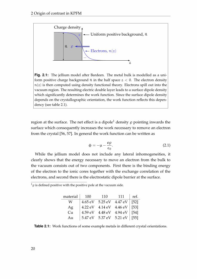
In the model of Bardeen - the jellium model - a free electron gas on a uniformpositive charge background is used to describe metallic materials. The electrondensity is left free to relax, while the positive background is kept fix. At the sur-face an abrupt step in the background charge occurs. The electron density willexponentially tail out into the vacuum region, leaving a slightly positive charged
19
2 Origin of contrast in KPFM
Electrons, n(z)
Uniform positive background, n
Charge density
n
z
−
+
℘
Fig. 2.1: The jellium model after Bardeen. The metal bulk is modelled as a uni-form positive charge background n in the half space z < 0. The electron densityn(z) is then computed using density functional theory. Electrons spill out into thevacuum region. The resulting electric double layer leads to a surface dipole densitywhich significantly determines the work function. Since the surface dipole densitydepends on the crystallographic orientation, the work function reflects this depen-dency (see table 2.1).
region at the surface. The net effect is a dipole1 density ℘ pointing inwards thesurface which consequently increases the work necessary to remove an electronfrom the crystal [56, 57]. In general the work function can be written as
φ = −µ−e℘
ε0. (2.1)
While the jellium model does not include any lateral inhomogeneities, itclearly shows that the energy necessary to move an electron from the bulk tothe vacuum consists out of two components. First there is the binding energyof the electron to the ionic cores together with the exchange correlation of theelectrons, and second there is the electrostatic dipole barrier at the surface.
1℘ is defined positive with the positive pole at the vacuum side.
material 100 110 111 ref.W 4.65 eV 5.25 eV 4.47 eV [52]Ag 4.22 eV 4.14 eV 4.46 eV [53]Cu 4.59 eV 4.48 eV 4.94 eV [54]Au 5.47 eV 5.37 eV 5.21 eV [55]
Table 2.1: Work functions of some example metals in different crystal orientations.
20
2.1 Metal surfaces - initial contrast
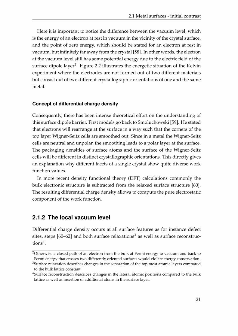
Here it is important to notice the difference between the vacuum level, whichis the energy of an electron at rest in vacuum in the vicinity of the crystal surface,and the point of zero energy, which should be stated for an electron at rest invacuum, but infinitely far away from the crystal [58]. In other words, the electronat the vacuum level still has some potential energy due to the electric field of thesurface dipole layer2. Figure 2.2 illustrates the energetic situation of the Kelvinexperiment where the electrodes are not formed out of two different materialsbut consist out of two different crystallographic orientations of one and the samemetal.
Concept of differential charge density
Consequently, there has been intense theoretical effort on the understanding ofthis surface dipole barrier. First models go back to Smoluchowski [59]. He statedthat electrons will rearrange at the surface in a way such that the corners of thetop layer Wigner-Seitz cells are smoothed out. Since in a metal the Wigner-Seitzcells are neutral and unpolar, the smoothing leads to a polar layer at the surface.The packaging densities of surface atoms and the surface of the Wigner-Seitzcells will be different in distinct crystallographic orientations. This directly givesan explanation why different facets of a single crystal show quite diverse workfunction values.
In more recent density functional theory (DFT) calculations commonly thebulk electronic structure is subtracted from the relaxed surface structure [60].The resulting differential charge density allows to compute the pure electrostaticcomponent of the work function.
2.1.2 The local vacuum level
Differential charge density occurs at all surface features as for instance defectsites, steps [60–62] and both surface relaxations3 as well as surface reconstruc-tions4.
2Otherwise a closed path of an electron from the bulk at Fermi energy to vacuum and back toFermi energy that crosses two differently oriented surfaces would violate energy conservation.
3Surface relaxation describes changes in the separation of the top most atomic layers comparedto the bulk lattice constant.
4Surface reconstruction describes changes in the lateral atomic positions compared to the bulklattice as well as insertion of additional atoms in the surface layer.
21
2 Origin of contrast in KPFM
(a)
E110vl
E100vl
EF
φ110
(110)
φ100
(100)
(b)
E110vl
E100vl
EF
φ110
(110)
φ100
(100)
(c) Evl
E110F
E100F
U = (φ100 −φ110)/e
eU
φ110
(110)
φ100
(100)
Fig. 2.2: (a) The two uncharged electrodes of same material, each with its orienta-tion specific work function, are not connected but share the same material depen-dent Fermi energy EF. (b) Under metallic contact the Fermi level is common to thewhole system. Hence no charge will flow between the electrodes. The difference inthe vacuum levels and thus the electrostatic forces remain. (c) The electrostatic forceis compensated by an external voltageU = (φ100 −φ110)/e applied to the electrodes.
22
2.1 Metal surfaces - initial contrast
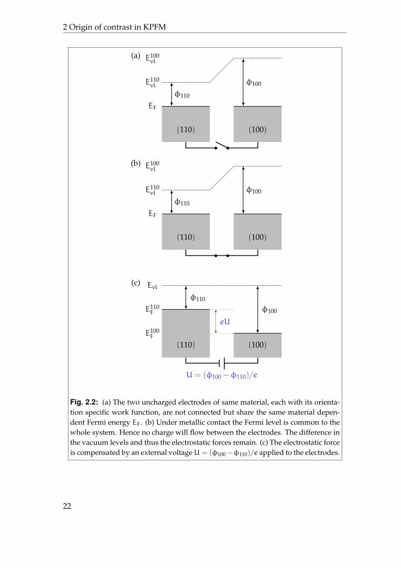
At this point, the advantage of Kelvin probe force microscopy becomes obvi-ous. Macroscopic experimental techniques like electron emission experimentsare non-local and therefore insensitive to the single surface feature. Only surfacedensities of for instance steps can significantly change the work function [63, 64].Nevertheless, in a microscopic technique like Kelvin probe force microscopy orscanning tunnelling microscopy the single feature can be resolved [65]. Thus,instead of dealing with an uniform vacuum level it is necessary to introduce alocal vacuum level which includes the electric potential of the surface features.On clean metallic samples these should indeed be the only sources for local con-trast in Kelvin probe force microscopy.
Also, the in general multi-polar differential charge density is not to be con-fused with free charges as the differential charge is a direct consequence of thequantum mechanic nature of the electron gas. Any external electric field whichoriginates from free charges will be screened according to the well known rulesof electrostatics.
2.1.3 Implications for KPFM
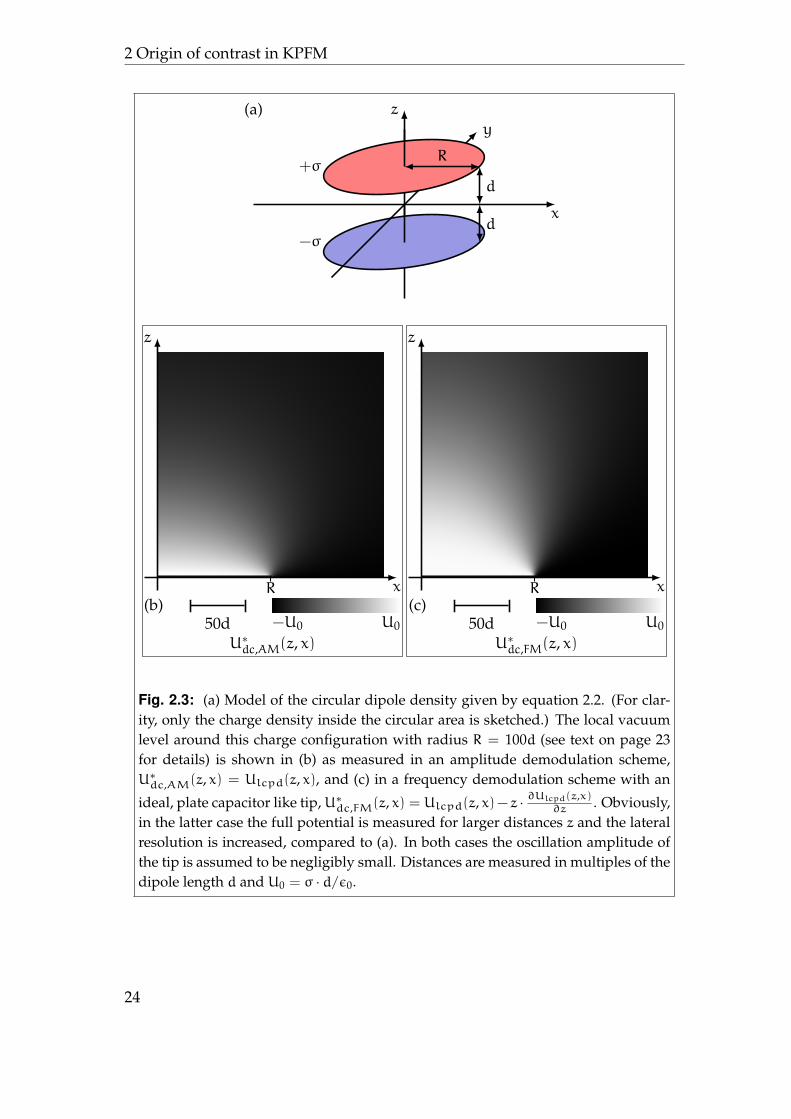
As mentioned above, variations in the local vacuum level as consequence of alateral variation of the differential charge density yields rise for lateral contrastin Kelvin probe force microscopy. Naturally, this also implies a vertical variationsince far away from the sample5 the potential variation has to vanish. Thus,there will be a z-dependence of the local contact potential difference. The decaylength of the potential is determined by the feature size.
In section 1.2.3 it was shown that a variation of the local contact potentialdifference with distance z can lead to differences in the measured voltage U∗dc.Again, amplitude demodulation methods measure in first order the local contactpotential difference at the equilibrium position of the ideal tip, while frequencydemodulation methods measure values closer to the surface at z = 0. For smallfeatures with short decay lengths frequency demodulation might thus offer bet-ter lateral resolution.
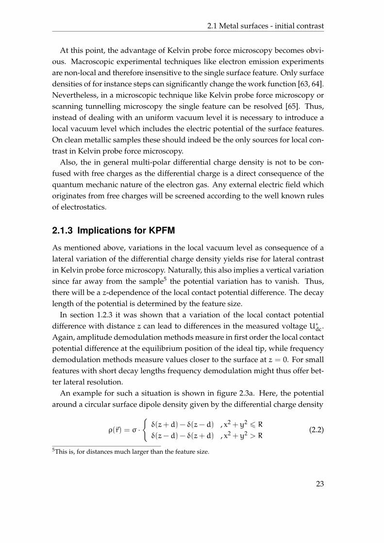
An example for such a situation is shown in figure 2.3a. Here, the potentialaround a circular surface dipole density given by the differential charge density
ρ(~r) = σ ·
{δ(z+ d) − δ(z− d) , x2 + y2 6 R
δ(z− d) − δ(z+ d) , x2 + y2 > R(2.2)
5This is, for distances much larger than the feature size.
23
2 Origin of contrast in KPFM
+σ
−σ
(a) z
x
y
R
d
d
z
xR(b)
50d −U0 U0
U∗dc,AM(z, x)
z
xR(c)
50d −U0 U0
U∗dc,FM(z, x)
Fig. 2.3: (a) Model of the circular dipole density given by equation 2.2. (For clar-ity, only the charge density inside the circular area is sketched.) The local vacuumlevel around this charge configuration with radius R = 100d (see text on page 23for details) is shown in (b) as measured in an amplitude demodulation scheme,U∗dc,AM(z, x) = Ulcpd(z, x), and (c) in a frequency demodulation scheme with an
ideal, plate capacitor like tip,U∗dc,FM(z, x) = Ulcpd(z, x)− z ·∂Ulcpd(z,x)
∂z . Obviously,in the latter case the full potential is measured for larger distances z and the lateralresolution is increased, compared to (a). In both cases the oscillation amplitude ofthe tip is assumed to be negligibly small. Distances are measured in multiples of thedipole length d and U0 = σ · d/ε0.
24

2.2 Metal/adsorbate-systems - adsorbate driven contrast
with radius R is computed6 and a cut in the x-z-plane is plotted. Both, height zand distance x are measured in multiples of the dipole length d. Figure 2.3b alsoresembles the value measured by amplitude demodulation methods with theideal point like tip in gradient approximation. In figure 2.3c the same situationis shown for frequency demodulation detection furthermore assuming a platecapacitor like tip.
Similar calculations have been carried out by Zerweck et al. [29]. There, themain difference in the computation is, that a fixed voltage between tip and sam-ple instead of a fixed dipole density at the sample surface is considered. Hence,the earlier results can not savagely be applied to variations of the local vacuumlevel. The statement of quantitative correct values in frequency demodulationmethods seems disputable in the here discussed case, as also discussed in sec-tion 1.2.3. Nevertheless, the finding that frequency demodulation offers higherlateral resolution holds true.
2.2 Metal/adsorbate-systems - adsorbate drivencontrast
Since the early experiments of Lord Kelvin it is known that adsorbates can signif-icantly change the work function of a metal. For example, work function tuningwas of great interest for the development of thermionic electron sources as alowered work function increases the electron output [66]. In present nanotech-nology, tailoring of contact work functions is important in device optimisationfor instance in organic light emitting devices [67, 68]. Naturally, Kelvin probeforce microscopy is a suitable tool to study adsorbate effects. In the following,first monolayers of inorganic adsorbates and later on of organic adsorbates areconsidered.
2.2.1 Inorganic adsorbates
While virtually any material can change the work function of a given substrate,the effects that can take place can be classified in three categories. Normally, theobserved changes will be a result of a mixture of these effects and they mightbe summarised as a difference in the surface dipole density. Besides an initial
6See also appendix C.
25
2 Origin of contrast in KPFM
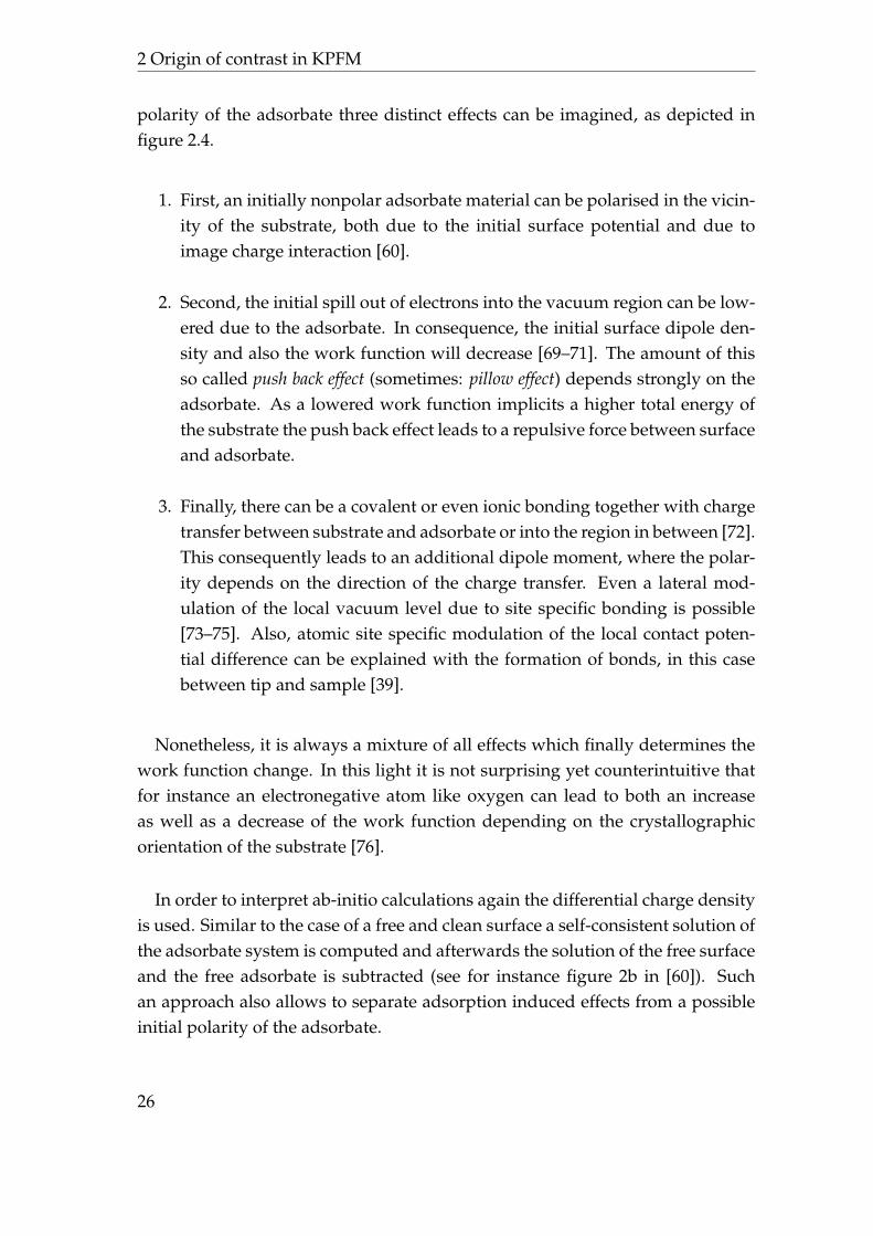
polarity of the adsorbate three distinct effects can be imagined, as depicted infigure 2.4.
1. First, an initially nonpolar adsorbate material can be polarised in the vicin-ity of the substrate, both due to the initial surface potential and due toimage charge interaction [60].
2. Second, the initial spill out of electrons into the vacuum region can be low-ered due to the adsorbate. In consequence, the initial surface dipole den-sity and also the work function will decrease [69–71]. The amount of thisso called push back effect (sometimes: pillow effect) depends strongly on theadsorbate. As a lowered work function implicits a higher total energy ofthe substrate the push back effect leads to a repulsive force between surfaceand adsorbate.
3. Finally, there can be a covalent or even ionic bonding together with chargetransfer between substrate and adsorbate or into the region in between [72].This consequently leads to an additional dipole moment, where the polar-ity depends on the direction of the charge transfer. Even a lateral mod-ulation of the local vacuum level due to site specific bonding is possible[73–75]. Also, atomic site specific modulation of the local contact poten-tial difference can be explained with the formation of bonds, in this casebetween tip and sample [39].
Nonetheless, it is always a mixture of all effects which finally determines thework function change. In this light it is not surprising yet counterintuitive thatfor instance an electronegative atom like oxygen can lead to both an increaseas well as a decrease of the work function depending on the crystallographicorientation of the substrate [76].
In order to interpret ab-initio calculations again the differential charge densityis used. Similar to the case of a free and clean surface a self-consistent solution ofthe adsorbate system is computed and afterwards the solution of the free surfaceand the free adsorbate is subtracted (see for instance figure 2b in [60]). Suchan approach also allows to separate adsorption induced effects from a possibleinitial polarity of the adsorbate.
26
2.2 Metal/adsorbate-systems - adsorbate driven contrast
(a) Polarisation of adsorbate due to surface charge
−
+
℘
−
+
℘℘′+ −
+ −
+ −
+ −
∆φ > 0
(b) Polarisation of adsorbate due to image charge
- + -- + -
- + -- + -
+−++−+
+−++−+
− + -− + -
− + -− + -
℘′
∆φ < 0
(c) Pushback effect
−
+
℘
−
+
℘′
∆φ < 0
(d) Charge transfer
℘′
+ −
+ −
+ −
+ −
+ −∆φ > 0
℘′
+−
+−
+−
+−
+−
∆φ < 0
Fig. 2.4: Schematic drawing of the three distinct effects that change the work func-tion of a metal substrate under adsorption of a second material. The adsorbate canbecome polarised (a) by the electric field of the substrate’s surface dipole densityor (b) by image charge interaction. (b) Due to the adsorbed material part of thespill-out electrons are pushed back into the metal. Hence, the surface dipole den-sity is lowered. (c) Electrons are at least partly transferred between substrate andadsorbate or into the gap in between. The resulting change of the surface dipoledensity depends on the sign of the charge transfer. In general all effects can occursimultaneously.
27
2 Origin of contrast in KPFM
2.2.2 Organic adsorbates
While in principle the same effects as for inorganic adsorbates take place [58, 77–81], organic adsorbates lead to a higher complexity of the work function prob-lem. Nearly all molecules exhibit very anisotropic properties concerning bond-ing, initial polarity and polarisability. Furthermore, especially organic semicon-ductors are characterized with ionisation potentials in the same energy range asmetal work functions. Thus, charge transfer under adsorption is commonly ob-served even for physisorbed materials [82]. Also, the exact location of the trans-ferred charges on the adsorbed molecules is important, as initially present or un-der adsorption generated dipoles can be completely screened by the additionalcharge [83, 84]. Obviously, the observed work function change of a molecularlayer is somewhat averaged since the confinement of differential charge densityon the location of the adsorbed molecule evokes variations of the local vacuumlevel on the (sub)molecular scale. These have been observed with Kelvin probeforce microscopy in some rare cases [85].
2.2.3 Implications for KPFM
Besides the molecular structure of organic adsorbate layers, lateral contrast inKelvin probe force microscopy images will occur between regions with differentadsorbate coverage or adsorbate properties. Due to the manifold mechanismswhich finally lead to the overall work function change the precise correlationbetween theory and experiment becomes challenging. When measured localcontact potential differences shall be interpreted, a profound knowledge of thestudied system is inevitable. Especially counteracting effects like the push backeffect and electron transfer onto the adsorbate can lead to misinterpretation asfor instance both effects can cancel out each other completely [80, 83]. Again,a vertical variation of the local contact potential around the adsorbate induceddifferential charge density and the previous described consequences for the dif-ferent imaging techniques have to be expected.
28

2.3 Insulating systems – polarisation induced contrast
2.3 Insulating systems – polarisation inducedcontrast
Especially insulating materials are interesting for scanning force microscopy asthey can not easily be studied by scanning tunnelling microscopy. From an elec-trostatic point of view simple insulators are fully characterized by their dielectrictensor and will only change the tip-sample capacitance. Nevertheless, they areof great importance in electric devices, can support free charges and in specialcases even exhibit free polarisation.
2.3.1 Free charge
Free, localized charges are of great interest in Kelvin probe force microscopy.Charges bound to the tip lead to significant shifts of the totally measured localcontact potential difference. This is one reason, why only lateral image contrastscan be evaluated since typically the charge state of the tip is unknown. If chargesare localized on the sample they will lead to image contrast [21, 22, 25].
In literature quite a number of approximative solutions can be found for thisspecial electrostatic problem [19, 20, 32, 86–89]. In the following, only the mostimportant results of the very general Green’s function ansatz used by Kan-torovich et al. shall be quoted [19]. For an arrangement of metal electrodes,each supported by a fixed potential, and free, localized charges qi, one finds aneffective potential Ueff by which the electrostatic force is given as
~F = −∂Ueff∂~r
. (2.3)
This effective potential Ueff is a result of the direct electrostatic interactionbetween the metal electrodes 7, the direct interaction of the charges qi with theelectrodes and finally the indirect interaction between the charges qi via theirimage potentials on the metals. In the case of just two electrodes, like in thetypical Kelvin probe setup, it can be written as
Ueff = −12C(~r) ·U2 + u1(~r) ·U+ u2(~r), (2.4)
with the capacitance C of and the applied voltage U between tip and sample. u1
describes the interaction of the charges qi with the electrodes while u2 contains
7It also includes the voltage supplies which support the potentials on the electrodes.
29
2 Origin of contrast in KPFM
the indirect interaction. The resulting electrostatic force in z-direction is givenby
Fel(~r) = +12∂C(~r)
∂z·U2 −
∂u1(~r)
∂z·U−
∂u2(~r)
∂z(2.5)
=12∂C(~r)
∂z
(U−
∂u1(~r)∂z∂C(~r)∂z
)2
−∂u2(~r)
∂z−
12
(∂u1(~r)∂z
)2
∂C(~r)∂z
. (2.6)
The comparison between equation 1.10 and 2.6 shows, that the free charges qiwill induce a shift of the local contact potential difference
∆Ulcpd(~r) = −∂u1(~r)∂z∂C(~r)∂z
. (2.7)
This shift depends on both the position of the charges relative to the electrodesand the capacitance between the latter. Further, the image force part of the elec-trostatic interaction can not be compensated with the applied voltage U. There-fore a complete annihilation of electrostatic force interaction becomes impossiblein the case of free, localized charges.
2.3.2 Free polarisation
Besides their function as mechanical support for free charge, insulating layerscan exhibit free polarisation. Such materials are called polar. A subclass arethe ferroelectric materials which are characterized by the fact, that the remanentpolarisation ~Pr can be switched by an external electric field [90]. For the firsttime, ferroelectricity was found in Rochelle-salt in 1920 [91]. Since then, manyother materials with ferroelectric properties have been studied [92].
The ferroelectric polarisation is constricted to certain axes in the crystal lattice.For every single axis two possible orientations can be found. In order to min-imize the free energy connected to the remanent polarisation field in a crystal,domains build up [93]. The actual size and distribution of the domains is in-fluenced by many facts as for instance the material itself, geometric propertiesof the actual crystal, strain fields, electric fields, temperature, and their history[94]. Goal of Kelvin probe force microscopy is the surface potential UP whichoriginates from the domain distribution given by
UP =Pzr · dfεε0
, (2.8)
30
2.3 Insulating systems – polarisation induced contrast
(a)
Pr
df d
ε
Udc
−
−
−
σS
(b)ϕel
z
UP
0
U∗dc
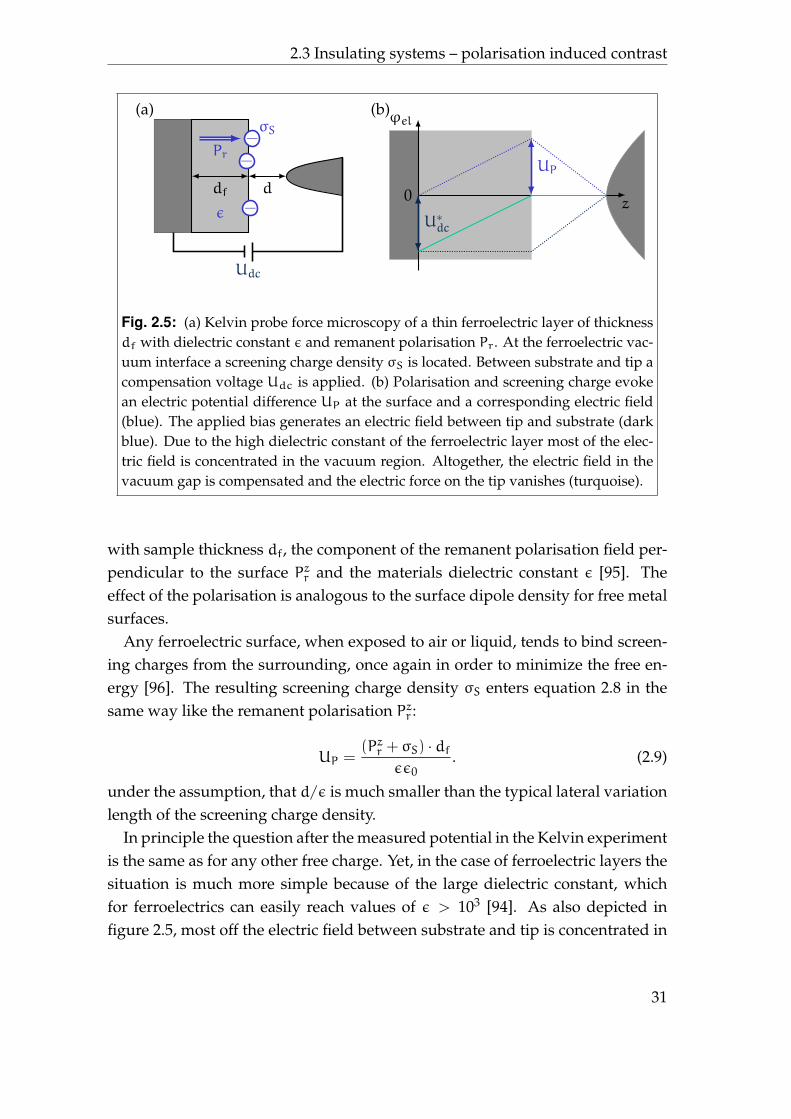
Fig. 2.5: (a) Kelvin probe force microscopy of a thin ferroelectric layer of thicknessdf with dielectric constant ε and remanent polarisation Pr. At the ferroelectric vac-uum interface a screening charge density σS is located. Between substrate and tip acompensation voltage Udc is applied. (b) Polarisation and screening charge evokean electric potential difference UP at the surface and a corresponding electric field(blue). The applied bias generates an electric field between tip and substrate (darkblue). Due to the high dielectric constant of the ferroelectric layer most of the elec-tric field is concentrated in the vacuum region. Altogether, the electric field in thevacuum gap is compensated and the electric force on the tip vanishes (turquoise).
with sample thickness df, the component of the remanent polarisation field per-pendicular to the surface Pzr and the materials dielectric constant ε [95]. Theeffect of the polarisation is analogous to the surface dipole density for free metalsurfaces.
Any ferroelectric surface, when exposed to air or liquid, tends to bind screen-ing charges from the surrounding, once again in order to minimize the free en-ergy [96]. The resulting screening charge density σS enters equation 2.8 in thesame way like the remanent polarisation Pzr :
UP =(Pzr + σS) · df
εε0. (2.9)
under the assumption, that d/ε is much smaller than the typical lateral variationlength of the screening charge density.
In principle the question after the measured potential in the Kelvin experimentis the same as for any other free charge. Yet, in the case of ferroelectric layers thesituation is much more simple because of the large dielectric constant, whichfor ferroelectrics can easily reach values of ε > 103 [94]. As also depicted infigure 2.5, most off the electric field between substrate and tip is concentrated in
31
2 Origin of contrast in KPFM
the vacuum gap and therefore the difference between UP and the measured U∗dchappens to be small8.
As a direct consequence of equation 2.9 an image contrast can be generated bya domain distribution, lateral variation of the screening charge density and vari-ation of the dielectric tensor in the layer. Thus, a direct analysis of Kelvin probeforce microscopy images is only possible with additional knowledge about themicroscopic nature of sample.
2.3.3 Compound systems
In many experiments a combination of insulators, free metal surfaces and ad-sorbates eventually connected to different external voltage sources are studied.Especially investigations of interfaces between metallic electrodes and organicmaterials are a keystone for the understanding of new organic electronic devices[97–100].
Of special interest is the organic field effect transistor [101–103]. The mostimportant information that can be derived from Kelvin probe force microscopyinvestigations are the potential distribution in the channel region and voltagedrops due to contact resistivity [46–48, 104–108], or voltage drops connected toinhomogeneities [109] and grain boundaries [110–112] of the organic layer.
As seen in the previous sections the insulating layer can lead to some pecu-liarities as a potential, measured in the gap region, can have different origins.Either, the potential is caused by free charges, if the organic layer is in an insu-lating state, or it is given by the external applied voltages and the work functiondifference between the tip and the organic in the conducting state. For a flawlessanalysis, therefore, also a measurement of the involved currents is necessary.
2.4 Summary
Contrast in Kelvin probe force microscopy has many origins. On clean metalsthese are local changes of the vacuum level due to a variation of the surfacedipole density. Similar, also inhomogeneous coverage with adsorbate causes alocal contrasts. A complete understanding of the measured contact potentialdifferences is subject to theory, as many distinct effects lead to changes in theobserved differential charge density.8With layer thickness df and minimal tip-surface distance d the systematic, relative error will beproportional to df
ε·d .
32

2.4 Summary
Insulating layers can either generate contrast if they consist of polar (in a morespecial case ferroelectric) materials or serve as a support for free charges. Con-trast and resolution are given by the solution of the classic electrostatic problem.Finally all effects come together in studies of compound systems, as will be re-ported in the second part of this work.
In the following, examples shall be given for each of the observable effectsranging from the pristine Au(111) surface to organic thin films on ferroelectricsubstrates.
33


Part II
Visualisation of Local ChargeDensities

3 Experiment
A theory is something nobody believes, except the per-son who made it. An experiment is something every-body believes, except the person who made it.
Albert Einstein
In order to prove the hypothesis, that a lateral variation of a multi-polar differ-ential charge density at the surface of the conductive sample leads to the observ-able contrast in Kelvin probe force microscopy, experiments were carried outwith the setup described below. The most simple system to start with, wouldnaturally be a pristine metal surface which can exhibit steps, defects and sur-face reconstructions. In this work, Gold was chosen to demonstrate the differenteffects and the results will be described in chapter 4.
Afterwards, the more complex situation of organic adsorbates on metals ispresented in chapter 5 with to examples, namely: dibutyl sexithiophene on goldand octachloro zinc phthalocyanine on silver. The differential charge densitymodel will successfully be applied to explain the contact potential contrast be-tween different structural phases of the octachloro zinc phthalocyanine on silver.
Finally, the constraints of the model are discussed for thin films of ferroelec-tric lead zirconate titanate. Besides pristine lead zirconate titanate thin films theinfluence of cleaning procedures and organic adsorbate layers on the observedcontact potential contrast will be investigated in chapters 6 and 7, respectively.
All experiments shown here were accomplished in a modified LT-UHV-SFMmanufactured by the Omicron Nanotechnology GmbH. In the beginning theSCALA control electronics from Omicron together with a digital phase lockedloop developed by Prof. Ch. Loppacher were used to perform non-contactatomic force microscopy [11, 113]. Two additional lock-in amplifiers and onemore controller were necessary to implement the Kelvin probe force microscopy[29]. Later on, the complete electronics were changed to the SPM-1000 togetherwith the PllPro2 manufactured by the RHK Technology Inc. This now enables to
37
3 Experiment
perform a direct sideband demodulation. For a detailed description on how torun Kelvin probe force microscopy with this electronics see the appendix B.
The modifications of the original LT-UHV-SFM are as follows:
• The scan head has been mounted with an additional spring system in orderto improve vibrational insulation.
• The interferometer photo current-to-voltage amplifier has been replacedby a homebuilt version. Therewith the detection bandwidth was increasedfrom ≈ 300 kHz to ≈ 3 MHz.
• An additional low vacuum storage vessel1 was installed between the tur-bomolecular pump and the roughing pump such that the roughing pumpcan be switched off during the measurement.
Mostly, cantilevers of the PPP-NCL or PPP-NCH series from Nanosensors™have been used. In order to remove the native oxide on the tip they were etchedin 5% hydrofluoric acid for one to two minutes.
Data analysis was performed with the free Gwyddion2 software in its version2.22. All given potential values were extracted from the original data, partly af-ter application of a Gaussian filter, and are given as the mean value in the areaof interest. The standard deviation of the potential fluctuations, which measurestypically 10 mV – 30 mV, is taken as error estimate for the single value. Ac-cordingly, lateral potential differences are measured with an accuracy of about20 mV – 60 mV. The accuracy of the method can be increased, when the band-width of the used electronics is decreased. Unfortunately, also the maximumpossible scan speed is reduced at the same time, which in practical applicationssets a lower bound of the bandwidth at about 125 Hz3. The measured potentialfluctuations are due to noise in the detection electronics. As in principle an en-ergy difference is measured, the error estimate might also be compared to thethermal energy Etherm. = kT of about ≈ 6 meV at T = 80 K4.
1A 50 l steel keg sponsored by the Freiberger Brauerei AG. www.freibergerpils.de2See http://gwyddion.net/3The typical pixel frequency of 256 points per line in 2 seconds.4Needless to say, that the uncertainty is magnitudes larger than the quantum limit ∆E > h
2∆t ofabout ≈ 4 · 10−11 meV for the given measurement bandwidth.
38
4 Pristine metal surfaces
Dig where the gold is . . . unless you just need some ex-ercise.John M. Capozzi
In section 2.1 it was shown that surface features like steps or a surface recon-structions can cause contrast in Kelvin probe force microscopy. The origin is a lo-cal multi-polar charge density connected to these features. It is well known thatthe Au(111)-surface is reconstructed [114]. The large periodicity length of thereconstruction pattern and the chemical stability of gold are reasons to chooseAu(111) in order to study these effects. The used gold single crystal1 was pre-pared by repeated cycles of Ar+-sputtering and annealing2. All measurementswere performed at 80 K sample temperature.
4.1 Au(111) - surface steps
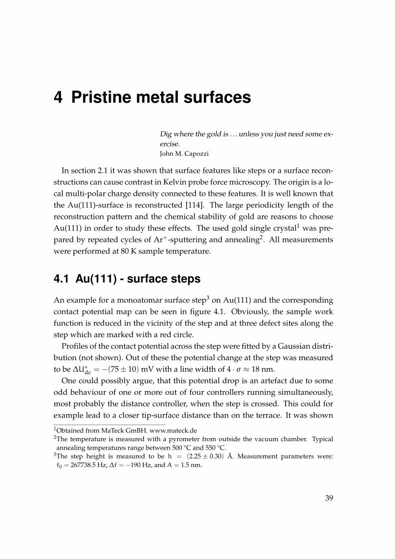
An example for a monoatomar surface step3 on Au(111) and the correspondingcontact potential map can be seen in figure 4.1. Obviously, the sample workfunction is reduced in the vicinity of the step and at three defect sites along thestep which are marked with a red circle.
Profiles of the contact potential across the step were fitted by a Gaussian distri-bution (not shown). Out of these the potential change at the step was measuredto be ∆U∗dc = −(75± 10) mV with a line width of 4 · σ ≈ 18 nm.
One could possibly argue, that this potential drop is an artefact due to someodd behaviour of one or more out of four controllers running simultaneously,most probably the distance controller, when the step is crossed. This could forexample lead to a closer tip-surface distance than on the terrace. It was shown
1Obtained from MaTeck GmBH. www.mateck.de2The temperature is measured with a pyrometer from outside the vacuum chamber. Typicalannealing temperatures range between 500 °C and 550 °C.
3The step height is measured to be h = (2.25 ± 0.30) A. Measurement parameters were:f0 = 267738.5 Hz, ∆f = −190 Hz, and A = 1.5 nm.
39
4 Pristine metal surfaces
(a)100 nm 0.0 nm 0.6 nm
topography
(b)100 nm 1.3 V 1.6 V
contact potential
(c)
x / nm
ϕ(x|z) / V-2 -1 0 1 2 3
-0.1
-0.2
z = 2 nmz = 1 nmz = 0.5 nmz = 0.2 nm
Fig. 4.1: Pristine Au(111)-surface. (a) Topography image. In the lower right cornera second gold terrace starts. (b) The corresponding contact potential image. Stepsand defect sites at the steps (marked by red circles) reduce the work function. Thestep site is measured with a reduced potential of∆U∗dc = −(75± 10) mV. (c) The cal-culated potential at an Au(111) step site caused by the corresponding linear dipoledensity as described by equation 4.1. The parameters are l = 2.35 A, d = 2.88 Aand p = 0.2 D / step atom. The local potential change extends about 1 nm to eachside of the step. As can be seen the measured value of ∆U∗dc = −(75± 10) mV isreasonable while the measured line width is far too wide by a factor of 10 due to theconvolution of the tip geometry with the actual potential distribution.Parameters: f0 = 267738.5 Hz, A = 1.5 nm, ∆f = −190 Hz.
40
4.1 Au(111) - surface steps
by Sadewasser et al. [115] that possible influences of the pure topography ontothe measured potential are negligibly small for reasonable step heights. Hence,in the case of a monoatomar step such artefacts have not to be expected.
Work function reduction due to surface steps on gold has been reported be-fore. Besocke et al. [63] found in a macroscopic study with low energy elec-tron diffraction Auger electron spectroscopy a linear decrease of the work func-tion with growing step density and an associated step dipole moment density ofp = 0.2 . . . 0.27 D / step atom. Investigations of gold steps with scanning tun-nelling microscopy derived a similar value of p = (0.16± 0.05) D / step atommeasured on a single step [65]. There, a model for the potential around the stepdipole is given:
ϕel(x, z) =Q
4πε0ln
((z+ l
2
)2+ x2(
z− l2
)2+ x2
), (4.1)
where Q denotes the linear density of charge running in y-direction and l is thedistance between positive and negative charge. The direction is taken such thatthe positive pole lies at the vacuum side.
Let d be the spacing of the step atoms, d = 2.88 A for Au(111); then theinduced dipole moment can be calculated as p = Qdl per step atom. The dipolelength l can be taken to be approximately the step height4 [61, 62]. In figure4.1c several potential profiles computed with equation 4.1 and the above givenparameters are shown for different heights z above the centre of the dipole den-sity. As can be seen the measured value of ∆U∗dc = −(75± 10) mV is reasonablewhile the line width is not because of the convolution of the tip geometry withthe actual potential distribution. A second example is given in the appendix Din figure D.1.
In conclusion, the local potential caused by the redistribution of metal elec-trons at surface steps as described by the Smoluchowski effect can be imagedwith Kelvin probe force microscopy. Due to the highly localised potential dis-tribution a typical Kelvin probe force microscopy resolution of ≈ 10 nm is notsufficient to quantitatively deduce the step dipole density.
4For the case of Au(111) l = 2.35 A.
41
4 Pristine metal surfaces
4.2 Au(111) - surface reconstruction I
The surface reconstruction of gold has been studied extensively [114, 116–118].As for many other metal surfaces a tensile stress in the first atomic layer leadsto a contractive quasi-one dimensional reconstruction for Au(111) [119, 120]. Asdepicted in figure 4.2, atoms are contracted along the 〈110〉-direction by about4.3 percent which leads to an insertion of one additional atom on 22 atoms of thesecond layer. In the perpendicular 〈112〉-direction surface atoms stay in registrywith the underlying bulk plane.
This anisotropy cannot be explained by means of the surface stress only[121, 122]. In the case of Au(111) the bulk substrate potential is significant com-pared to other metals and therefore the accommodation between the bulk andthe surface layer happens through the induction of dislocations. After the dislo-cation energy criterion of Frank, the stablest dislocation is given by the smallestnorm of the Burgers vector [123]. In the face-centred cubic (fcc) lattice of a (111)plane this is ~b(1/2)〈110〉 =
12〈110〉. This corresponds to sliding a part of the sur-
face atoms along the 〈110〉-direction and insertion of an additional line of atomsrunning in the 〈121〉-direction.
Yet there is another low-energy stacking fault in the (111) plane given by~b(1/6)〈121〉 = 1
6〈121〉. Therefore the perfect dislocation can dissociate into twoimperfect dislocations
12〈110〉 ⇒ 1
6〈121〉+ 1
6〈211〉, (4.2)
which finally further reduces the elastic strain energy of the surface layer [124].Each of these imperfect dislocations can be recognised as a Shockley partial dis-location which describes a stacking shift of the surface layer from face-centredcubic to hexagonal close-packed (hcp). The transition area, where atoms arefound in a bridge position, is known as discommensuration line. As two of theseShockley partial dislocations are involved, the reconstruction of the Au(111) sur-face is characterised by a pair of discommensuration lines and a shift from fccto hcp and back to fcc stacking every 22 bulk atoms which equals to 70 A in〈110〉-direction. Due to the Franck energy criterion only one out of three possibleBurgers vectors is expected, which explains the observed contraction anisotropy.Consequently also three energetically equal reconstruction orientations are pos-sible. For large areas the stripe domain reconstruction becomes unstable becauseof this threefold orientational degeneracy. The result is the familiar zigzag pat-
42
4.2 Au(111) - surface reconstruction I
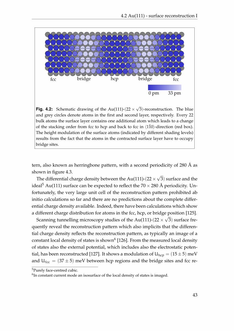
0 pm 33 pm
fcc bridge hcp bridge fcc
Fig. 4.2: Schematic drawing of the Au(111)-(22 ×√
3)-reconstruction. The blueand grey circles denote atoms in the first and second layer, respectively. Every 22bulk atoms the surface layer contains one additional atom which leads to a changeof the stacking order from fcc to hcp and back to fcc in 〈110〉-direction (red box).The height modulation of the surface atoms (indicated by different shading levels)results from the fact that the atoms in the contracted surface layer have to occupybridge sites.
tern, also known as herringbone pattern, with a second periodicity of 280 A asshown in figure 4.3.
The differential charge density between the Au(111)-(22×√
3) surface and theideal5 Au(111) surface can be expected to reflect the 70× 280 A periodicity. Un-fortunately, the very large unit cell of the reconstruction pattern prohibited abinitio calculations so far and there are no predictions about the complete differ-ential charge density available. Indeed, there have been calculations which showa different charge distribution for atoms in the fcc, hcp, or bridge position [125].
Scanning tunnelling microscopy studies of the Au(111)-(22×√
3) surface fre-quently reveal the reconstruction pattern which also implicits that the differen-tial charge density reflects the reconstruction pattern, as typically an image of aconstant local density of states is shown6 [126]. From the measured local densityof states also the external potential, which includes also the electrostatic poten-tial, has been reconstructed [127]. It shows a modulation ofUhcp = (15± 5) meVand Ufcc = (37± 5) meV between hcp regions and the bridge sites and fcc re-
5Purely face-centred cubic.6In constant current mode an isosurface of the local density of states is imaged.
43
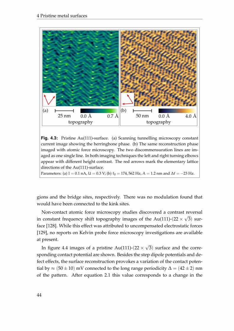
4 Pristine metal surfaces
(a)25 nm 0.0 A 0.7 A
topography
(b)50 nm 0.0 A 4.0 A
topography
Fig. 4.3: Pristine Au(111)-surface. (a) Scanning tunnelling microscopy constantcurrent image showing the herringbone phase. (b) The same reconstruction phaseimaged with atomic force microscopy. The two discommensuration lines are im-aged as one single line. In both imaging techniques the left and right turning elbowsappear with different height contrast. The red arrows mark the elementary latticedirections of the Au(111)-surface.Parameters: (a) I = 0.1 nA, U = 0.3 V; (b) f0 = 174, 562 Hz, A = 1.2 nm and ∆f = −23 Hz.
gions and the bridge sites, respectively. There was no modulation found thatwould have been connected to the kink sites.
Non-contact atomic force microscopy studies discovered a contrast reversalin constant frequency shift topography images of the Au(111)-(22 ×
√3) sur-
face [128]. While this effect was attributed to uncompensated electrostatic forces[129], no reports on Kelvin probe force microscopy investigations are availableat present.
In figure 4.4 images of a pristine Au(111)-(22 ×√
3) surface and the corre-sponding contact potential are shown. Besides the step dipole potentials and de-fect effects, the surface reconstruction provokes a variation of the contact poten-tial by ≈ (50± 10) mV connected to the long range periodicity ∆ = (42± 2) nmof the pattern. After equation 2.1 this value corresponds to a change in the
44
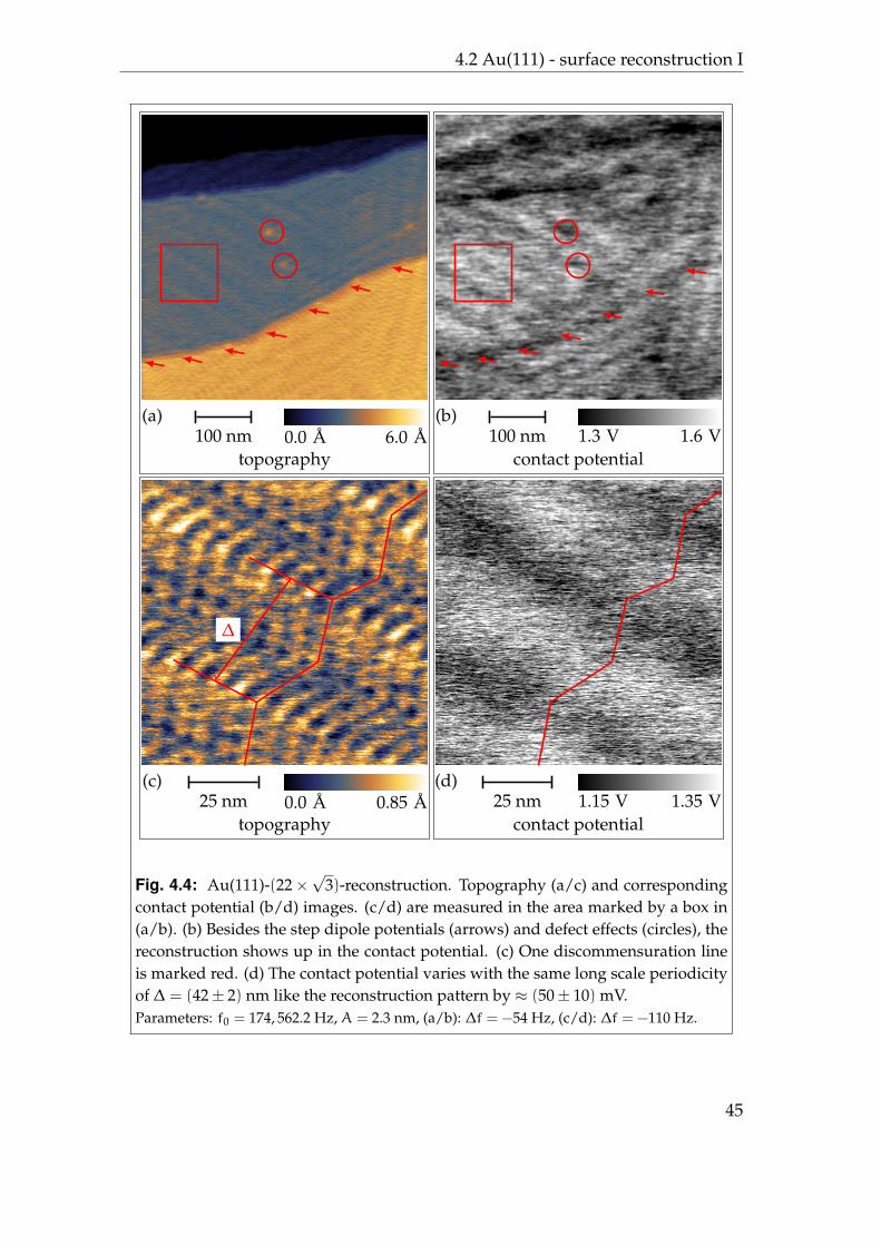
4.2 Au(111) - surface reconstruction I
(a)100 nm 0.0 A 6.0 A
topography
(b)100 nm 1.3 V 1.6 V
contact potential
∆
(c)25 nm 0.0 A 0.85 A
topography
(d)25 nm 1.15 V 1.35 V
contact potential
Fig. 4.4: Au(111)-(22×√
3)-reconstruction. Topography (a/c) and correspondingcontact potential (b/d) images. (c/d) are measured in the area marked by a box in(a/b). (b) Besides the step dipole potentials (arrows) and defect effects (circles), thereconstruction shows up in the contact potential. (c) One discommensuration lineis marked red. (d) The contact potential varies with the same long scale periodicityof ∆ = (42± 2) nm like the reconstruction pattern by ≈ (50± 10) mV.Parameters: f0 = 174, 562.2 Hz, A = 2.3 nm, (a/b): ∆f = −54 Hz, (c/d): ∆f = −110 Hz.
45
4 Pristine metal surfaces
metals surface dipole density of ∆℘ = (0.13± 0.03) D nm−2. Without a doubt themeasured values reflect only a lower boundary of the reconstruction inducedsurface dipole density variation due to the low lateral potential resolution of theimaging tip.Throughout many repetitions of the experiment always the areaswhich appear lower in the topography are characterised by a higher contactpotential. This is in accordance to the external potential reconstructed fromscanning tunnelling microscopy. The small scale potential variation of the dis-commensuration lines can hardly be resolved in experiment.
Au(111) happens to be a standard substrate in scanning probe microscopy tostudy the interaction between organic molecules and gold. A deeper knowledgeof the surface reconstruction and the local potential variations can help to un-derstand the driving forces behind the assembling of molecules. For instancethe kink sites have been shown to act as nucleation centres for the growth ofmetallic nanoclusters [130, 131]. Especially for Kelvin probe force microscopystudies of Au(111)/adsorbate systems the here reported potential variations areof great importance, yet have not been taken into account so far. The consider-able high electric fields which are associated to the potential variation might alsobe important for the description of catalytic processes.
4.3 Au(111) - surface reconstruction II
Compared to the very regular herringbone pattern, the situation turns out to bemuch more complicated when the Au(111) single crystal is annealed to lowertemperatures during the preparation cycles. A typical surface morphology afterannealing to 430 °C is shown in figure 4.5. Distinct areas each characterised by acertain morphology can be seen.
Most prominent appears the region labelled D in figure 4.5b. There a trigonaldot pattern alternates with triangular shaped “islands” in a rather random fash-ion. The dots have a spacing of (7.8± 0.2) nm and measure (20± 10) pm and(40± 10) pm in height compared to the cross and the hole position, respectively(see also figure 4.5c). Without any further measurable topographic contrast, theislands lie at the same height level as the adjacent area S2 which is like for thedots (40± 10) pm above the hole position. Remarkably the island borders arerelated to the dot positions in a way that orientation changes of the border occur
46
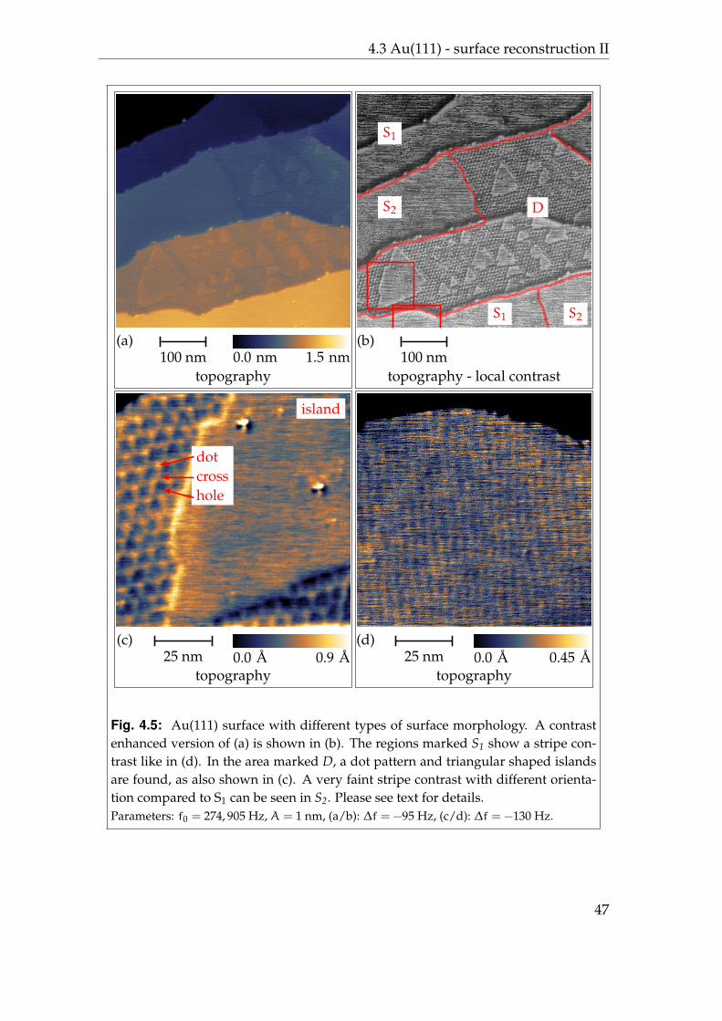
4.3 Au(111) - surface reconstruction II
(a)100 nm 0.0 nm 1.5 nm
topography
S1 S2
DS2
S1
(b)100 nm
topography - local contrast
dotcrosshole
island
(c)25 nm 0.0 A 0.9 A
topography
(d)25 nm 0.0 A 0.45 A
topography
Fig. 4.5: Au(111) surface with different types of surface morphology. A contrastenhanced version of (a) is shown in (b). The regions marked S1 show a stripe con-trast like in (d). In the area marked D, a dot pattern and triangular shaped islandsare found, as also shown in (c). A very faint stripe contrast with different orienta-tion compared to S1 can be seen in S2. Please see text for details.Parameters: f0 = 274, 905 Hz, A = 1 nm, (a/b): ∆f = −95 Hz, (c/d): ∆f = −130 Hz.
47
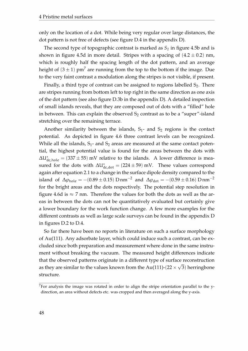
4 Pristine metal surfaces
only on the location of a dot. While being very regular over large distances, thedot pattern is not free of defects (see figure D.4 in the appendix D).
The second type of topographic contrast is marked as S1 in figure 4.5b and isshown in figure 4.5d in more detail. Stripes with a spacing of (4.2 ± 0.2) nm,which is roughly half the spacing length of the dot pattern, and an averageheight of (3± 1) pm7 are running from the top to the bottom if the image. Dueto the very faint contrast a modulation along the stripes is not visible, if present.
Finally, a third type of contrast can be assigned to regions labelled S2. Thereare stripes running from bottom left to top right in the same direction as one axisof the dot pattern (see also figure D.3b in the appendix D). A detailed inspectionof small islands reveals, that they are composed out of dots with a “filled” holein between. This can explain the observed S2 contrast as to be a “super”-islandstretching over the remaining terrace.
Another similarity between the islands, S1- and S2 regions is the contactpotential. As depicted in figure 4.6 three contrast levels can be recognized.While all the islands, S1- and S2 areas are measured at the same contact poten-tial, the highest potential value is found for the areas between the dots with∆U∗dc,hole = (337± 55) mV relative to the islands. A lower difference is mea-sured for the dots with ∆U∗dc,dot = (224± 59) mV. These values correspondagain after equation 2.1 to a change in the surface dipole density compared to theisland of ∆℘hole = −(0.89± 0.15) D nm−2 and ∆℘dot = −(0.59± 0.16) D nm−2
for the bright areas and the dots respectively. The potential step resolution infigure 4.6d is ≈ 7 nm. Therefore the values for both the dots as well as the ar-eas in between the dots can not be quantitatively evaluated but certainly givea lower boundary for the work function change. A few more examples for thedifferent contrasts as well as large scale surveys can be found in the appendix Din figures D.2 to D.4.
So far there have been no reports in literature on such a surface morphologyof Au(111). Any adsorbate layer, which could induce such a contrast, can be ex-cluded since both preparation and measurement where done in the same instru-ment without breaking the vacuum. The measured height differences indicatethat the observed patterns originate in a different type of surface reconstructionas they are similar to the values known from the Au(111)-(22×
√3) herringbone
structure.
7For analysis the image was rotated in order to align the stripe orientation parallel to the y-direction, an area without defects etc. was cropped and then averaged along the y-axis.
48
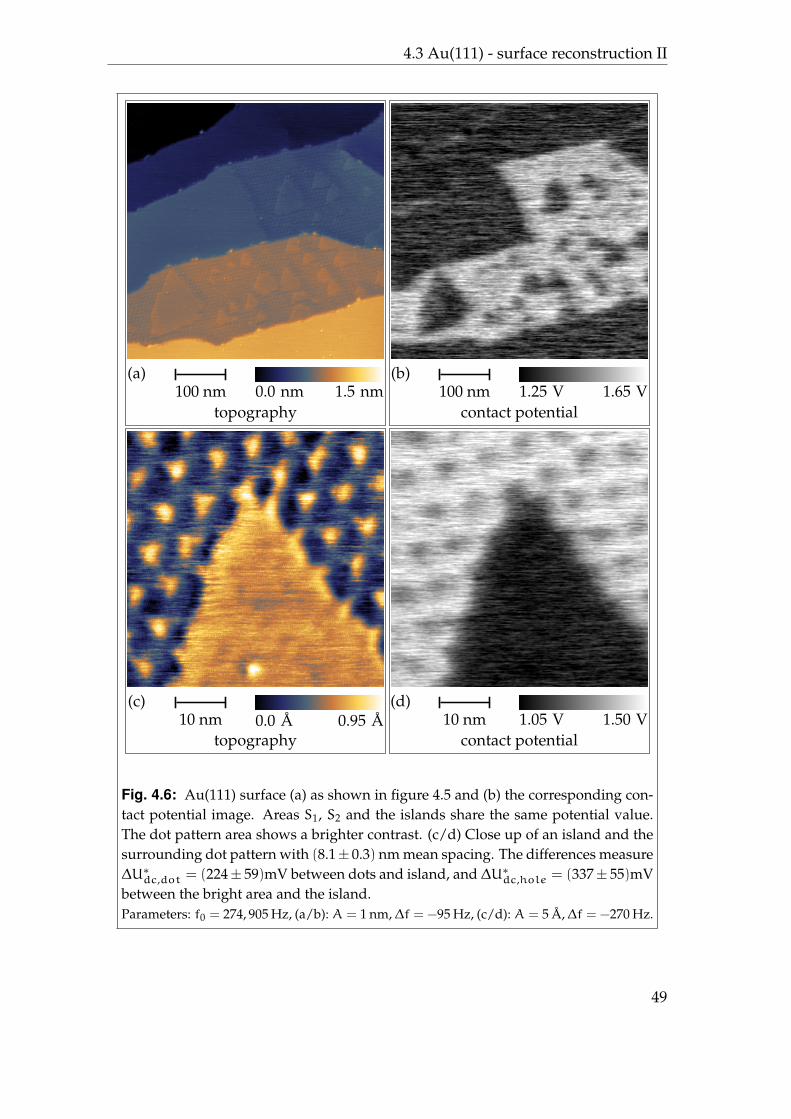
4.3 Au(111) - surface reconstruction II
(a)100 nm 0.0 nm 1.5 nm
topography
(b)100 nm 1.25 V 1.65 V
contact potential
(c)10 nm 0.0 A 0.95 A
topography
(d)10 nm 1.05 V 1.50 V
contact potential
Fig. 4.6: Au(111) surface (a) as shown in figure 4.5 and (b) the corresponding con-tact potential image. Areas S1, S2 and the islands share the same potential value.The dot pattern area shows a brighter contrast. (c/d) Close up of an island and thesurrounding dot pattern with (8.1± 0.3) nm mean spacing. The differences measure∆U∗dc,dot = (224± 59)mV between dots and island, and ∆U∗dc,hole = (337± 55)mVbetween the bright area and the island.Parameters: f0 = 274, 905 Hz, (a/b): A = 1 nm,∆f = −95 Hz, (c/d): A = 5 A,∆f = −270 Hz.
49
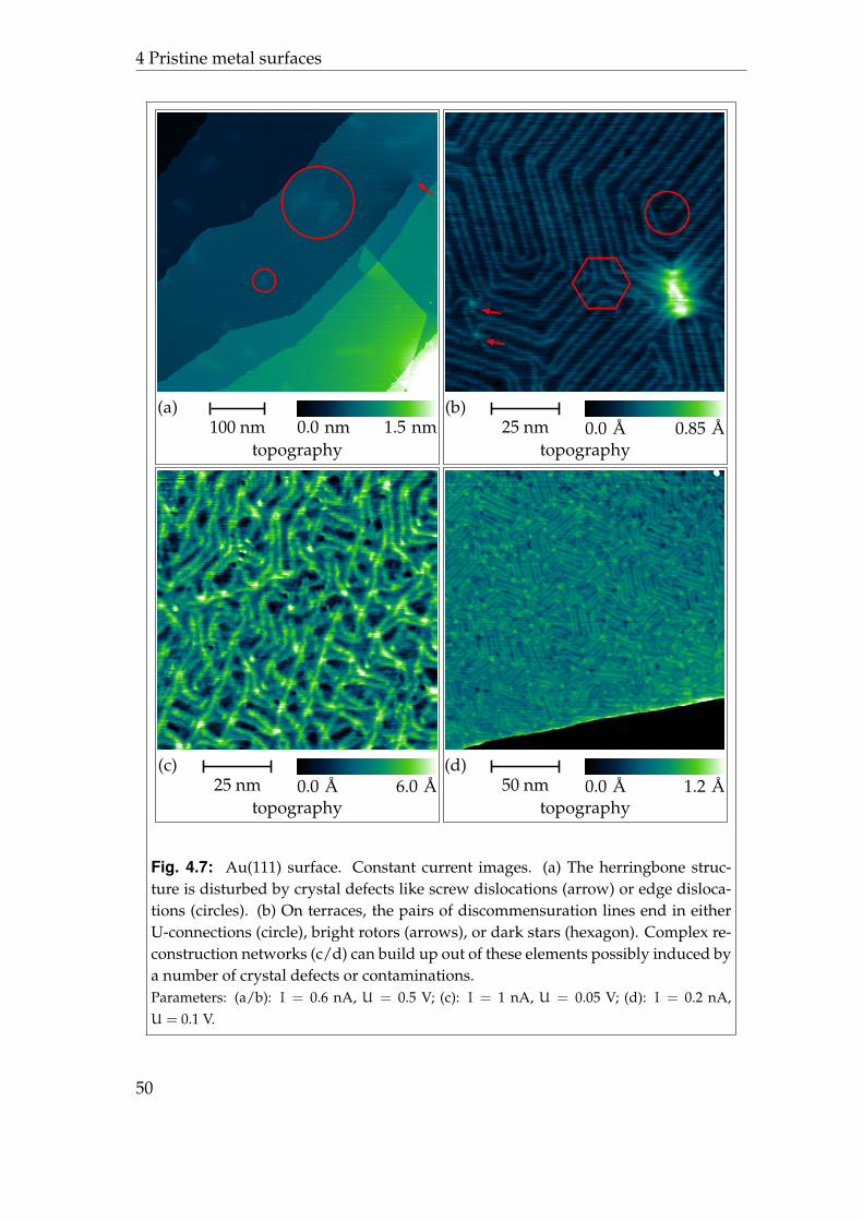
4 Pristine metal surfaces
(a)100 nm 0.0 nm 1.5 nm
topography
(b)25 nm 0.0 A 0.85 A
topography
(c)25 nm 0.0 A 6.0 A
topography
(d)50 nm 0.0 A 1.2 A
topography
Fig. 4.7: Au(111) surface. Constant current images. (a) The herringbone struc-ture is disturbed by crystal defects like screw dislocations (arrow) or edge disloca-tions (circles). (b) On terraces, the pairs of discommensuration lines end in eitherU-connections (circle), bright rotors (arrows), or dark stars (hexagon). Complex re-construction networks (c/d) can build up out of these elements possibly induced bya number of crystal defects or contaminations.Parameters: (a/b): I = 0.6 nA, U = 0.5 V; (c): I = 1 nA, U = 0.05 V; (d): I = 0.2 nA,U = 0.1 V.
50
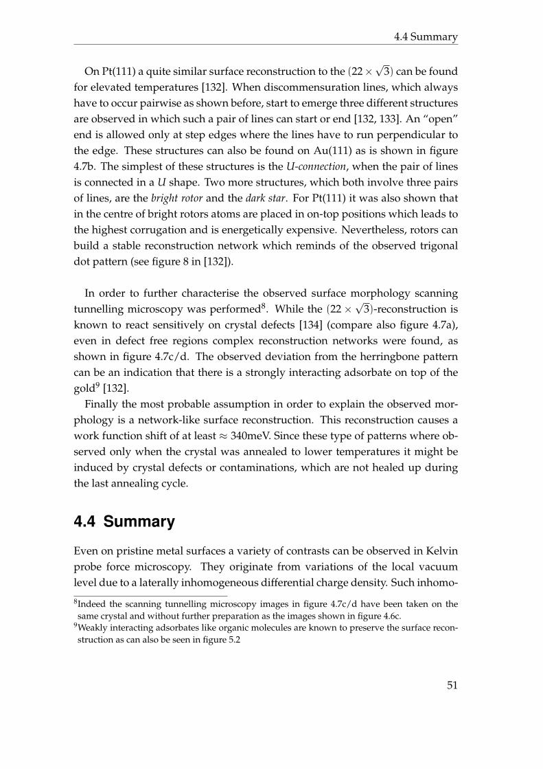
4.4 Summary
On Pt(111) a quite similar surface reconstruction to the (22×√
3) can be foundfor elevated temperatures [132]. When discommensuration lines, which alwayshave to occur pairwise as shown before, start to emerge three different structuresare observed in which such a pair of lines can start or end [132, 133]. An “open”end is allowed only at step edges where the lines have to run perpendicular tothe edge. These structures can also be found on Au(111) as is shown in figure4.7b. The simplest of these structures is the U-connection, when the pair of linesis connected in a U shape. Two more structures, which both involve three pairsof lines, are the bright rotor and the dark star. For Pt(111) it was also shown thatin the centre of bright rotors atoms are placed in on-top positions which leads tothe highest corrugation and is energetically expensive. Nevertheless, rotors canbuild a stable reconstruction network which reminds of the observed trigonaldot pattern (see figure 8 in [132]).
In order to further characterise the observed surface morphology scanningtunnelling microscopy was performed8. While the (22×
√3)-reconstruction is
known to react sensitively on crystal defects [134] (compare also figure 4.7a),even in defect free regions complex reconstruction networks were found, asshown in figure 4.7c/d. The observed deviation from the herringbone patterncan be an indication that there is a strongly interacting adsorbate on top of thegold9 [132].
Finally the most probable assumption in order to explain the observed mor-phology is a network-like surface reconstruction. This reconstruction causes awork function shift of at least ≈ 340meV. Since these type of patterns where ob-served only when the crystal was annealed to lower temperatures it might beinduced by crystal defects or contaminations, which are not healed up duringthe last annealing cycle.
4.4 Summary
Even on pristine metal surfaces a variety of contrasts can be observed in Kelvinprobe force microscopy. They originate from variations of the local vacuumlevel due to a laterally inhomogeneous differential charge density. Such inhomo-
8Indeed the scanning tunnelling microscopy images in figure 4.7c/d have been taken on thesame crystal and without further preparation as the images shown in figure 4.6c.
9Weakly interacting adsorbates like organic molecules are known to preserve the surface recon-struction as can also be seen in figure 5.2
51
4 Pristine metal surfaces
geneities are caused by defects, step dipoles and surface reconstructions, whichlead to a localisation of electron density in clear contrast to the picture of an elec-tron gas with a featureless density. Typical feature sizes are below the resolutionlimit of the Kelvin probe force microscope such that the measured values aremostly not quantitative. Furthermore, the apparent changes of the local vacuumlevel vanish quickly with growing distance. Work function changes of up to afew hundred millivolt in the vicinity of surface reconstructions together with thestrong localisation indicate high electric fields which are important for the self-assembling of adsorbates or catalytic reactions. Therefore Kelvin probe forcemicroscopy offers information which can help to study the physics behind suchprocesses in greater detail.
52
5 Metal/adsorbate-systems
A discovery is said to be an accident meeting a pre-pared mind.
Albert Szent-Gyorgyi
The understanding of interfaces between metals and other materials is mostimportant for current micro- and nanotechnology since structure sizes andtherewith the volume-to-surface ratios became constantly smaller over the pastdecades. Especially for electronic devices, properties of material interfaces cansignificantly change or even determine the device performance. Kelvin probeforce microscopy is widely used to study the electronic properties of such inter-faces. In the following, examples of metal/organic interfaces shall be shown andanalysed, namely: dibutyl sexithiophene on gold and octachloro zinc phthalo-cyanine on silver.
5.1 Au(111)/dibutyl sexithiophene
In recent organic field effect transistor research thiophene derivates are candi-dates for high performance organic semiconductors both in the form of smallmolecules – oligomers – as well as polymers. In most organic electronic devicesproperties of metal/organic interfaces strongly influence charge carrier injectionand consequently the device performance. Especially gold is a common materialfor metallic parts of such devices. One possibility to improve the gold/organicinterface is to specifically tailor the properties of the organic semiconductor. Thetypical oligothiophene consists out of four to seven thiophene rings and can bemodified with different side- and end groups in order to increase the packag-ing density, improve the self-assembly properties, electronic properties or thestability against oxidation [135].β,β′-dibutyl sexithiophene (DB6T), as shown in figure 5.1, is a modified α-
sexithiophene1 (α-6T). The modification occurs through the attachment of butyl1A chain of six thiophene rings.
53
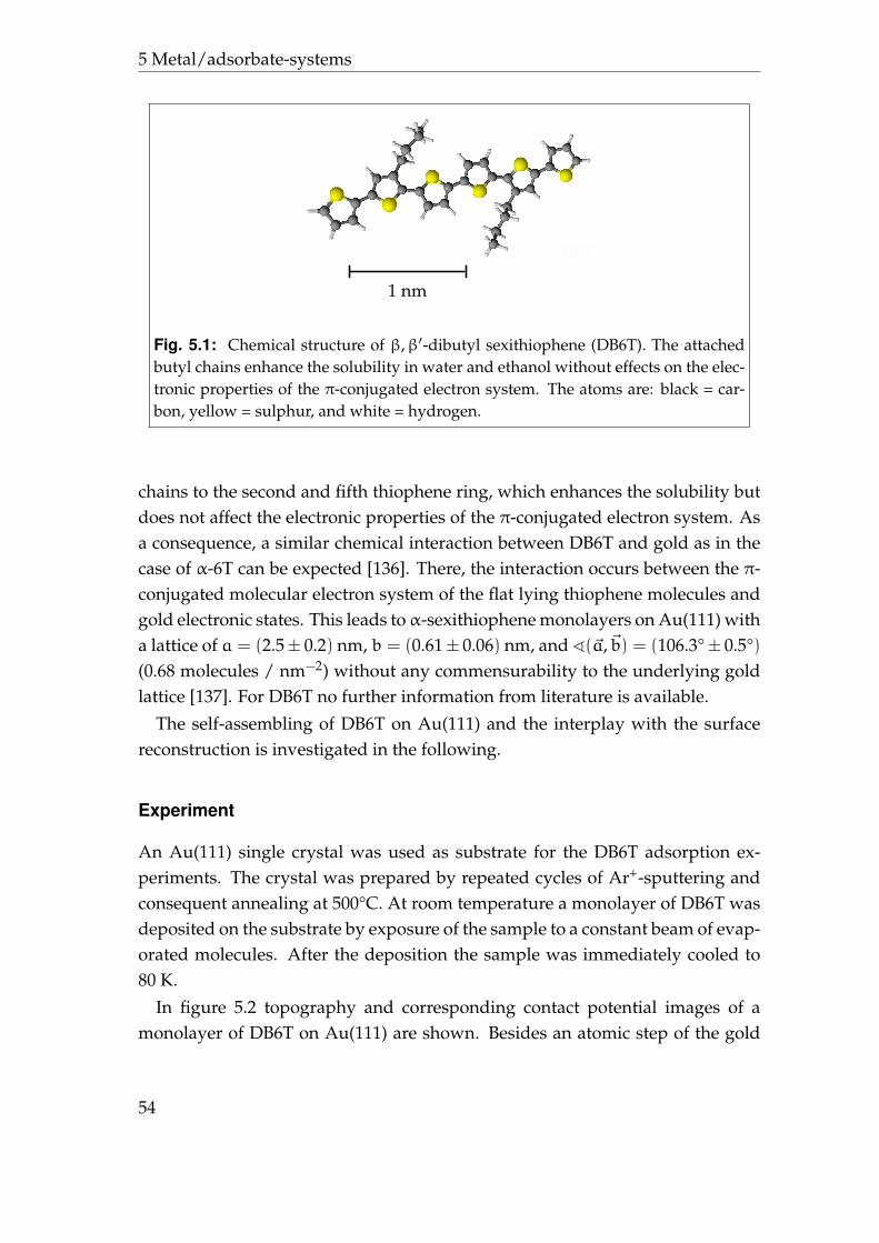
5 Metal/adsorbate-systems
1 nm
Fig. 5.1: Chemical structure of β,β′-dibutyl sexithiophene (DB6T). The attachedbutyl chains enhance the solubility in water and ethanol without effects on the elec-tronic properties of the π-conjugated electron system. The atoms are: black = car-bon, yellow = sulphur, and white = hydrogen.
chains to the second and fifth thiophene ring, which enhances the solubility butdoes not affect the electronic properties of the π-conjugated electron system. Asa consequence, a similar chemical interaction between DB6T and gold as in thecase of α-6T can be expected [136]. There, the interaction occurs between the π-conjugated molecular electron system of the flat lying thiophene molecules andgold electronic states. This leads toα-sexithiophene monolayers on Au(111) witha lattice of a = (2.5± 0.2) nm, b = (0.61± 0.06) nm, and ^(~a,~b) = (106.3°± 0.5°)(0.68 molecules / nm−2) without any commensurability to the underlying goldlattice [137]. For DB6T no further information from literature is available.
The self-assembling of DB6T on Au(111) and the interplay with the surfacereconstruction is investigated in the following.
Experiment
An Au(111) single crystal was used as substrate for the DB6T adsorption ex-periments. The crystal was prepared by repeated cycles of Ar+-sputtering andconsequent annealing at 500°C. At room temperature a monolayer of DB6T wasdeposited on the substrate by exposure of the sample to a constant beam of evap-orated molecules. After the deposition the sample was immediately cooled to80 K.
In figure 5.2 topography and corresponding contact potential images of amonolayer of DB6T on Au(111) are shown. Besides an atomic step of the gold
54
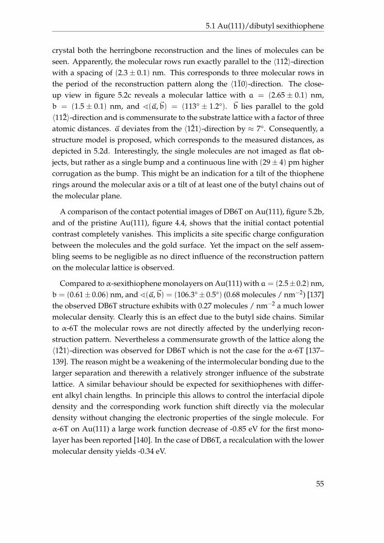
5.1 Au(111)/dibutyl sexithiophene
crystal both the herringbone reconstruction and the lines of molecules can beseen. Apparently, the molecular rows run exactly parallel to the 〈112〉-directionwith a spacing of (2.3± 0.1) nm. This corresponds to three molecular rows inthe period of the reconstruction pattern along the 〈110〉-direction. The close-up view in figure 5.2c reveals a molecular lattice with a = (2.65 ± 0.1) nm,b = (1.5 ± 0.1) nm, and ^(~a,~b) = (113° ± 1.2°). ~b lies parallel to the gold〈112〉-direction and is commensurate to the substrate lattice with a factor of threeatomic distances. ~a deviates from the 〈121〉-direction by ≈ 7°. Consequently, astructure model is proposed, which corresponds to the measured distances, asdepicted in 5.2d. Interestingly, the single molecules are not imaged as flat ob-jects, but rather as a single bump and a continuous line with (29± 4) pm highercorrugation as the bump. This might be an indication for a tilt of the thiophenerings around the molecular axis or a tilt of at least one of the butyl chains out ofthe molecular plane.
A comparison of the contact potential images of DB6T on Au(111), figure 5.2b,and of the pristine Au(111), figure 4.4, shows that the initial contact potentialcontrast completely vanishes. This implicits a site specific charge configurationbetween the molecules and the gold surface. Yet the impact on the self assem-bling seems to be negligible as no direct influence of the reconstruction patternon the molecular lattice is observed.
Compared toα-sexithiophene monolayers on Au(111) with a = (2.5±0.2) nm,b = (0.61± 0.06) nm, and ^(~a,~b) = (106.3°± 0.5°) (0.68 molecules / nm−2) [137]the observed DB6T structure exhibits with 0.27 molecules / nm−2 a much lowermolecular density. Clearly this is an effect due to the butyl side chains. Similarto α-6T the molecular rows are not directly affected by the underlying recon-struction pattern. Nevertheless a commensurate growth of the lattice along the〈121〉-direction was observed for DB6T which is not the case for the α-6T [137–139]. The reason might be a weakening of the intermolecular bonding due to thelarger separation and therewith a relatively stronger influence of the substratelattice. A similar behaviour should be expected for sexithiophenes with differ-ent alkyl chain lengths. In principle this allows to control the interfacial dipoledensity and the corresponding work function shift directly via the moleculardensity without changing the electronic properties of the single molecule. Forα-6T on Au(111) a large work function decrease of -0.85 eV for the first mono-layer has been reported [140]. In the case of DB6T, a recalculation with the lowermolecular density yields -0.34 eV.
55
5 Metal/adsorbate-systems
(a)20 nm 0.0 A 4.0 A
topography
(b)20 nm -0.9 V 0.4 V
contact potential
~a~b
(c)2 nm 0.0 A 1.3 A
topography
(d)2 nm
proposed structure model
~a~b
Fig. 5.2: (a) topography and (b) corresponding contact potential of a monolayerDB6T on Au(111). The lines of molecules run exactly parallel to the 〈112〉-direction.With a spacing of (2.3 ± 0.1) nm this corresponds to three molecular rows in theperiod of the reconstruction. (c) close up of the topography revealing the molecularlattice (a = (2.65± 0.1) nm, b = (1.5± 0.1) nm, and ^(~a,~b) = (113°± 1.2°)). (d)proposed structure model constructed to fit the measured distances.Parameters: f0 = 174, 562 Hz, (a/b): A = 1.2 nm, ∆f = −16 Hz, (c): ∆f = −34 Hz.
56
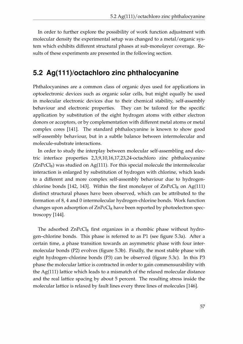
5.2 Ag(111)/octachloro zinc phthalocyanine
In order to further explore the possibility of work function adjustment withmolecular density the experimental setup was changed to a metal/organic sys-tem which exhibits different structural phases at sub-monolayer coverage. Re-sults of these experiments are presented in the following section.
5.2 Ag(111)/octachloro zinc phthalocyanine
Phthalocyanines are a common class of organic dyes used for applications inoptoelectronic devices such as organic solar cells, but might equally be usedin molecular electronic devices due to their chemical stability, self-assemblybehaviour and electronic properties. They can be tailored for the specificapplication by substitution of the eight hydrogen atoms with either electrondonors or acceptors, or by complementation with different metal atoms or metalcomplex cores [141]. The standard phthalocyanine is known to show goodself-assembly behaviour, but in a subtle balance between intermolecular andmolecule-substrate interactions.
In order to study the interplay between molecular self-assembling and elec-tric interface properties 2,3,9,10,16,17,23,24-octachloro zinc phthalocyanine(ZnPcCl8) was studied on Ag(111). For this special molecule the intermolecularinteraction is enlarged by substitution of hydrogen with chlorine, which leadsto a different and more complex self-assembly behaviour due to hydrogen-chlorine bonds [142, 143]. Within the first monolayer of ZnPcCl8 on Ag(111)distinct structural phases have been observed, which can be attributed to theformation of 8, 4 and 0 intermolecular hydrogen-chlorine bonds. Work functionchanges upon adsorption of ZnPcCl8 have been reported by photoelectron spec-troscopy [144].
The adsorbed ZnPcCl8 first organizes in a rhombic phase without hydro-gen–chlorine bonds. This phase is referred to as P1 (see figure 5.3a). After acertain time, a phase transition towards an asymmetric phase with four inter-molecular bonds (P2) evolves (figure 5.3b). Finally, the most stable phase witheight hydrogen–chlorine bonds (P3) can be observed (figure 5.3c). In this P3phase the molecular lattice is contracted in order to gain commensurability withthe Ag(111) lattice which leads to a mismatch of the relaxed molecular distanceand the real lattice spacing by about 5 percent. The resulting stress inside themolecular lattice is relaxed by fault lines every three lines of molecules [146].
57
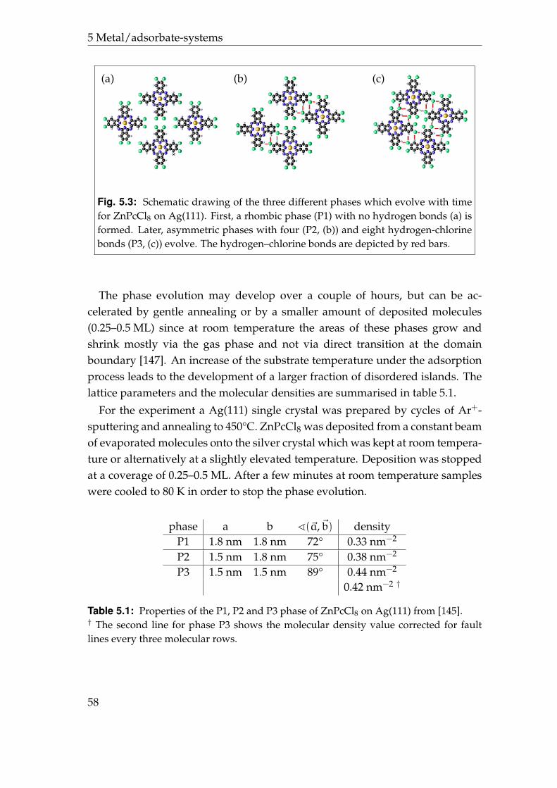
5 Metal/adsorbate-systems
(a) (b) (c)
Fig. 5.3: Schematic drawing of the three different phases which evolve with timefor ZnPcCl8 on Ag(111). First, a rhombic phase (P1) with no hydrogen bonds (a) isformed. Later, asymmetric phases with four (P2, (b)) and eight hydrogen-chlorinebonds (P3, (c)) evolve. The hydrogen–chlorine bonds are depicted by red bars.
The phase evolution may develop over a couple of hours, but can be ac-celerated by gentle annealing or by a smaller amount of deposited molecules(0.25–0.5 ML) since at room temperature the areas of these phases grow andshrink mostly via the gas phase and not via direct transition at the domainboundary [147]. An increase of the substrate temperature under the adsorptionprocess leads to the development of a larger fraction of disordered islands. Thelattice parameters and the molecular densities are summarised in table 5.1.
For the experiment a Ag(111) single crystal was prepared by cycles of Ar+-sputtering and annealing to 450°C. ZnPcCl8 was deposited from a constant beamof evaporated molecules onto the silver crystal which was kept at room tempera-ture or alternatively at a slightly elevated temperature. Deposition was stoppedat a coverage of 0.25–0.5 ML. After a few minutes at room temperature sampleswere cooled to 80 K in order to stop the phase evolution.
phase a b ^(~a,~b) densityP1 1.8 nm 1.8 nm 72° 0.33 nm−2
P2 1.5 nm 1.8 nm 75° 0.38 nm−2
P3 1.5 nm 1.5 nm 89° 0.44 nm−2
0.42 nm−2 †
Table 5.1: Properties of the P1, P2 and P3 phase of ZnPcCl8 on Ag(111) from [145].† The second line for phase P3 shows the molecular density value corrected for faultlines every three molecular rows.
58
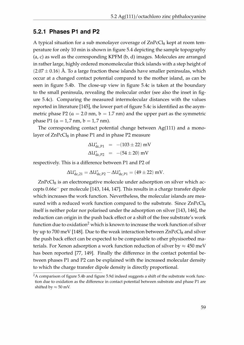
5.2 Ag(111)/octachloro zinc phthalocyanine
5.2.1 Phases P1 and P2
A typical situation for a sub monolayer coverage of ZnPcCl8 kept at room tem-perature for only 10 min is shown in figure 5.4 depicting the sample topography(a, c) as well as the corresponding KPFM (b, d) images. Molecules are arrangedin rather large, highly ordered monomolecular thick islands with a step height of(2.07± 0.16) A. To a large fraction these islands have smaller peninsulas, whichoccur at a changed contact potential compared to the mother island, as can beseen in figure 5.4b. The close-up view in figure 5.4c is taken at the boundaryto the small peninsula, revealing the molecular order (see also the inset in fig-ure 5.4c). Comparing the measured intermolecular distances with the valuesreported in literature [145], the lower part of figure 5.4c is identified as the asym-metric phase P2 (a = 2.0 nm, b = 1.7 nm) and the upper part as the symmetricphase P1 (a = 1, 7 nm, b = 1, 7 nm).
The corresponding contact potential change between Ag(111) and a mono-layer of ZnPcCl8 in phase P1 and in phase P2 measure
∆U∗dc,P1 = −(103± 22) mV
∆U∗dc,P2 = −(54± 20) mV
respectively. This is a difference between P1 and P2 of
∆U∗dc,21 = ∆U∗dc,P2 −∆U∗dc,P1 = (49± 22) mV.
ZnPcCl8 is an electronegative molecule under adsorption on silver which ac-cepts 0.66e− per molecule [143, 144, 147]. This results in a charge transfer dipolewhich increases the work function. Nevertheless, the molecular islands are mea-sured with a reduced work function compared to the substrate. Since ZnPcCl8itself is neither polar nor polarised under the adsorption on silver [143, 146], thereduction can origin in the push back effect or a shift of the free substrate’s workfunction due to oxidation2 which is known to increase the work function of silverby up to 700 meV [148]. Due to the weak interaction between ZnPcCl8 and silverthe push back effect can be expected to be comparable to other physisorbed ma-terials. For Xenon adsorption a work function reduction of silver by ≈ 450 meVhas been reported [77, 149]. Finally the difference in the contact potential be-tween phases P1 and P2 can be explained with the increased molecular densityto which the charge transfer dipole density is directly proportional.2A comparison of figure 5.4b and figure 5.9d indeed suggests a shift of the substrate work func-tion due to oxidation as the difference in contact potential between substrate and phase P1 areshifted by ≈ 50 mV.
59
5 Metal/adsorbate-systems
P1
P2
(a)50 nm 0.0 A 4.0 A
topography
P1
P2
(b)50 nm 1.87 V 2.05 V
contact potential
P1
P2
(c)25 nm 0.0 A 3.6 A
topography
P1
P2
(d)25 nm 1.89 V 2.05 V
contact potential
Fig. 5.4: ZnPcCl8 on Ag(111). (a) While the big island is already in phase P2 thesmall peninsula still shows phase P1. (b) The corresponding contact potential im-age. P1 and P2 appear at ∆U∗dc,P1 = −(103± 22) mV and ∆U∗dc,P2 = −(54± 20) mVrelative to the substrate respectively. (c/d) At the phase boundary a smooth transi-tion between phases P1 and P2 takes place (see also inset).Parameters: f0 = 161, 827 Hz, A = 1.3 nm, ∆f = −146 Hz.
60
5.2 Ag(111)/octachloro zinc phthalocyanine
After equations 2.1 and 1.29 the measured difference for sufficiently large is-lands is given by
∆U∗dc,21 = −1ε0
(℘P2 − ℘P1) . (5.1)
For a further analysis one might assume that the redistribution of metal sur-face electrons is more or less the same in both cases mostly because of the highinitial substrate coverage in phase P1. The charge transfer dipole density ℘ct
can be expressed by an average over the transferred charge density ρct(~r) in themolecular layer of height h [150]
℘ct =1A
∫A
d2xy
∫h0
dz z · ρct(~r) (5.2)
= σct · heff (5.3)
with an effective height heff and the surface density of transferred charge σct.This relates the difference in the charge density with the measured change in thecontact potential by
∆σct21 = −ε0 ·∆U∗dc,21
heff, (5.4)
since the monolayer height and the corresponding effective height are the samefor both phases.
According to literature heff can be set to heff = 0.5h [150]. Then (withh = (2.07± 0.16) A and ∆U∗dc,21 = (49 ± 22) mV being the measured values)the measured charge density difference equals ∆σct21 = (0.026± 0.014)e− nm−2,where the uncertainty originates mostly from the Kelvin voltage measure-ments. This has to be compared to the theoretical value of the transferredcharge of 0.66e− per molecule [147] and the change in molecular density asgiven in table 5.1. The so computed charge density difference ∆σct21,t equals∆σct21,t = (0.033± 0.002)e− nm−2, which is larger than the measured value butwell within the uncertainty range.
Again it has to be noted that a similar redistribution of metal electrons forboth phases has been assumed. A linear increase of the push back dipole den-sity with molecular coverage would lead to a less pronounced change of the con-tact potential evoked by the charge transfer, as both effects counteract. On theone hand, this would explain a smaller measured value than compared to theexpectation from theory, on the other hand, the small difference between the-ory and experiment (which is not significant due to the uncertainty connectedto the measurement) implicits that the variation of the push back dipole density
61
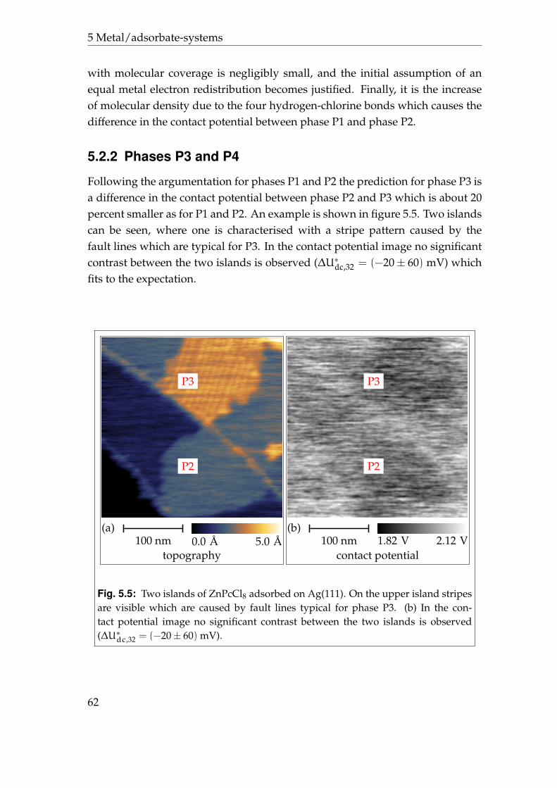
5 Metal/adsorbate-systems
with molecular coverage is negligibly small, and the initial assumption of anequal metal electron redistribution becomes justified. Finally, it is the increaseof molecular density due to the four hydrogen-chlorine bonds which causes thedifference in the contact potential between phase P1 and phase P2.
5.2.2 Phases P3 and P4
Following the argumentation for phases P1 and P2 the prediction for phase P3 isa difference in the contact potential between phase P2 and P3 which is about 20percent smaller as for P1 and P2. An example is shown in figure 5.5. Two islandscan be seen, where one is characterised with a stripe pattern caused by thefault lines which are typical for P3. In the contact potential image no significantcontrast between the two islands is observed (∆U∗dc,32 = (−20± 60) mV) whichfits to the expectation.
P3
P2
(a)100 nm 0.0 A 5.0 A
topography
P3
P2
(b)100 nm 1.82 V 2.12 V
contact potential
Fig. 5.5: Two islands of ZnPcCl8 adsorbed on Ag(111). On the upper island stripesare visible which are caused by fault lines typical for phase P3. (b) In the con-tact potential image no significant contrast between the two islands is observed(∆U∗dc,32 = (−20± 60) mV).
62
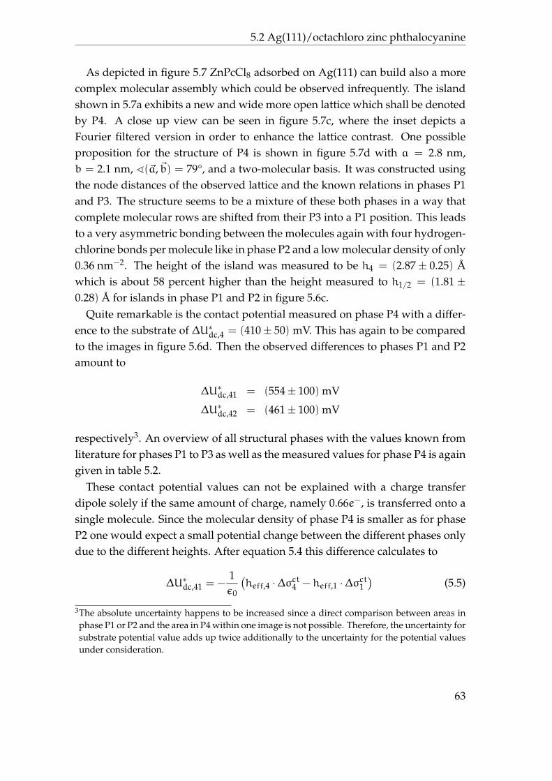
5.2 Ag(111)/octachloro zinc phthalocyanine
As depicted in figure 5.7 ZnPcCl8 adsorbed on Ag(111) can build also a morecomplex molecular assembly which could be observed infrequently. The islandshown in 5.7a exhibits a new and wide more open lattice which shall be denotedby P4. A close up view can be seen in figure 5.7c, where the inset depicts aFourier filtered version in order to enhance the lattice contrast. One possibleproposition for the structure of P4 is shown in figure 5.7d with a = 2.8 nm,b = 2.1 nm, ^(~a,~b) = 79°, and a two-molecular basis. It was constructed usingthe node distances of the observed lattice and the known relations in phases P1and P3. The structure seems to be a mixture of these both phases in a way thatcomplete molecular rows are shifted from their P3 into a P1 position. This leadsto a very asymmetric bonding between the molecules again with four hydrogen-chlorine bonds per molecule like in phase P2 and a low molecular density of only0.36 nm−2. The height of the island was measured to be h4 = (2.87± 0.25) Awhich is about 58 percent higher than the height measured to h1/2 = (1.81 ±0.28) A for islands in phase P1 and P2 in figure 5.6c.
Quite remarkable is the contact potential measured on phase P4 with a differ-ence to the substrate of ∆U∗dc,4 = (410± 50) mV. This has again to be comparedto the images in figure 5.6d. Then the observed differences to phases P1 and P2amount to
∆U∗dc,41 = (554± 100) mV
∆U∗dc,42 = (461± 100) mV
respectively3. An overview of all structural phases with the values known fromliterature for phases P1 to P3 as well as the measured values for phase P4 is againgiven in table 5.2.
These contact potential values can not be explained with a charge transferdipole solely if the same amount of charge, namely 0.66e−, is transferred onto asingle molecule. Since the molecular density of phase P4 is smaller as for phaseP2 one would expect a small potential change between the different phases onlydue to the different heights. After equation 5.4 this difference calculates to
∆U∗dc,41 = −1ε0
(heff,4 ·∆σct4 − heff,1 ·∆σct1
)(5.5)
3The absolute uncertainty happens to be increased since a direct comparison between areas inphase P1 or P2 and the area in P4 within one image is not possible. Therefore, the uncertainty forsubstrate potential value adds up twice additionally to the uncertainty for the potential valuesunder consideration.
63
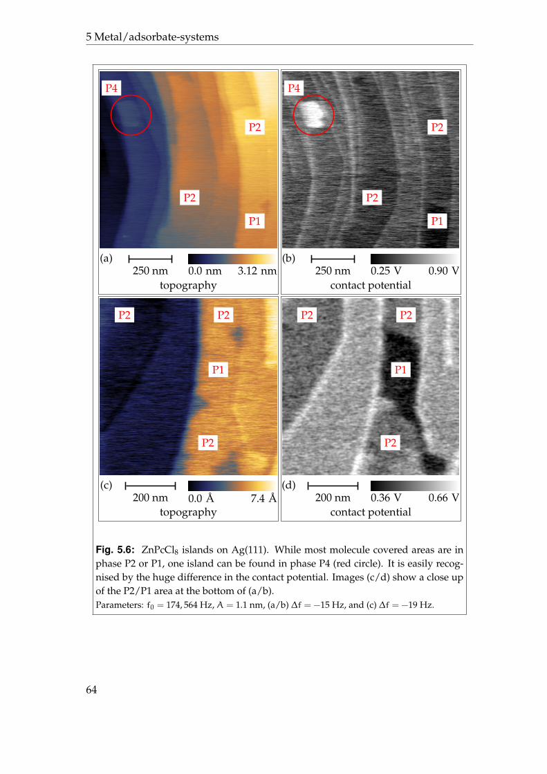
5 Metal/adsorbate-systems
P4
P2
P2
P1
(a)250 nm 0.0 nm 3.12 nm
topography
(b)
P4
P2
P2
P1
250 nm 0.25 V 0.90 Vcontact potential
P2 P2
P1
P2
(c)200 nm 0.0 A 7.4 A
topography
P2 P2
P1
P2
(d)200 nm 0.36 V 0.66 V
contact potential
Fig. 5.6: ZnPcCl8 islands on Ag(111). While most molecule covered areas are inphase P2 or P1, one island can be found in phase P4 (red circle). It is easily recog-nised by the huge difference in the contact potential. Images (c/d) show a close upof the P2/P1 area at the bottom of (a/b).Parameters: f0 = 174, 564 Hz, A = 1.1 nm, (a/b) ∆f = −15 Hz, and (c) ∆f = −19 Hz.
64
5.2 Ag(111)/octachloro zinc phthalocyanine
(a)50 nm 0.0 A 6.5 A
topography
(b)50 nm 0.6 V 1.15 V
contact potential
(c)10 nm 0.0 A 2.5 A
topography
(d)2 nm
proposed structure model
~a
~b
Fig. 5.7: (a) topography and (b) corresponding contact potential of a ZnPcCl8-island in a new phase P4 on Ag(111) (see text). The height and the contact potentialdifference measure (2.87± 25) A and (410± 50) mV respectively. (c) The molecularlattice consists of two molecules per unit cell. The inset shows a Fourier filteredversion of the topography. (d) proposed structure model (a = 2.8 nm, b = 2.1 nm,and ^(~a,~b) = 79°).Parameters: f0 = 174, 564 Hz, A = 1.1 nm, (a/b) ∆f = −16 Hz, and (c) ∆f = −26 Hz.
65
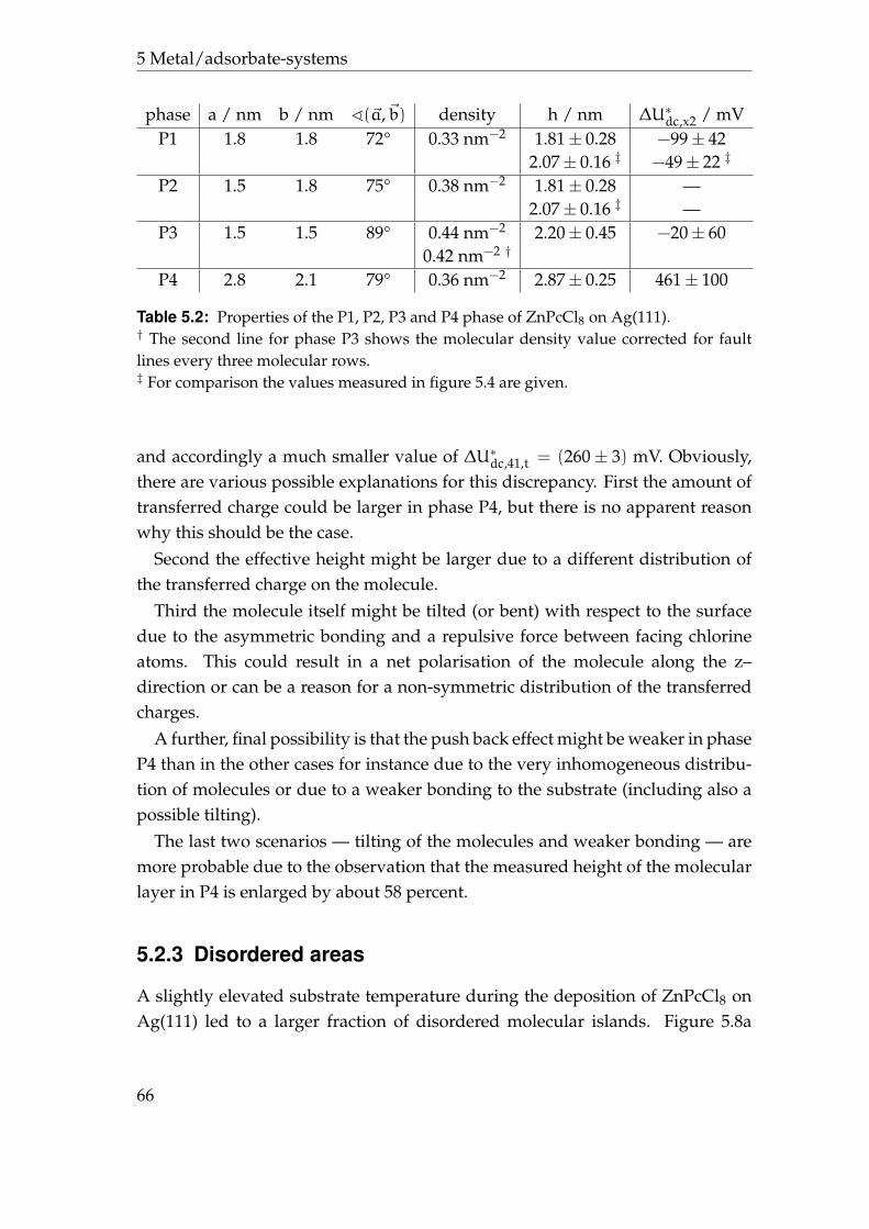
5 Metal/adsorbate-systems
phase a / nm b / nm ^(~a,~b) density h / nm ∆U∗dc,x2 / mVP1 1.8 1.8 72° 0.33 nm−2 1.81± 0.28 −99± 42
2.07± 0.16 ‡ −49± 22 ‡
P2 1.5 1.8 75° 0.38 nm−2 1.81± 0.28 —2.07± 0.16 ‡ —
P3 1.5 1.5 89° 0.44 nm−2 2.20± 0.45 −20± 600.42 nm−2 †
P4 2.8 2.1 79° 0.36 nm−2 2.87± 0.25 461± 100
Table 5.2: Properties of the P1, P2, P3 and P4 phase of ZnPcCl8 on Ag(111).† The second line for phase P3 shows the molecular density value corrected for faultlines every three molecular rows.‡ For comparison the values measured in figure 5.4 are given.
and accordingly a much smaller value of ∆U∗dc,41,t = (260± 3) mV. Obviously,there are various possible explanations for this discrepancy. First the amount oftransferred charge could be larger in phase P4, but there is no apparent reasonwhy this should be the case.
Second the effective height might be larger due to a different distribution ofthe transferred charge on the molecule.
Third the molecule itself might be tilted (or bent) with respect to the surfacedue to the asymmetric bonding and a repulsive force between facing chlorineatoms. This could result in a net polarisation of the molecule along the z–direction or can be a reason for a non-symmetric distribution of the transferredcharges.
A further, final possibility is that the push back effect might be weaker in phaseP4 than in the other cases for instance due to the very inhomogeneous distribu-tion of molecules or due to a weaker bonding to the substrate (including also apossible tilting).
The last two scenarios — tilting of the molecules and weaker bonding — aremore probable due to the observation that the measured height of the molecularlayer in P4 is enlarged by about 58 percent.
5.2.3 Disordered areas
A slightly elevated substrate temperature during the deposition of ZnPcCl8 onAg(111) led to a larger fraction of disordered molecular islands. Figure 5.8a
66
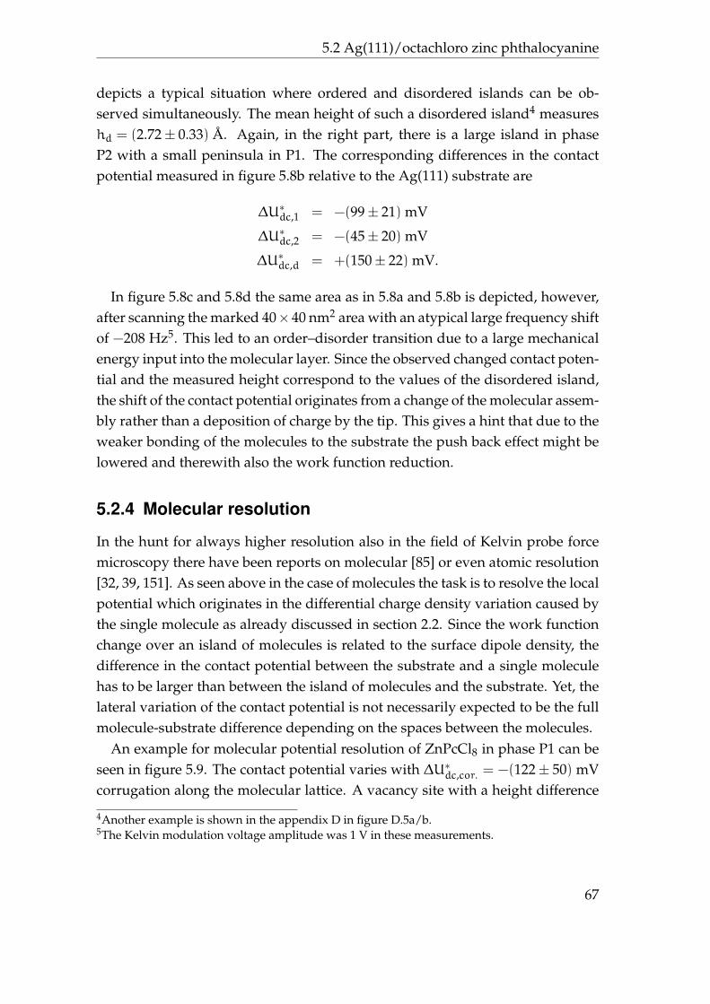
5.2 Ag(111)/octachloro zinc phthalocyanine
depicts a typical situation where ordered and disordered islands can be ob-served simultaneously. The mean height of such a disordered island4 measureshd = (2.72± 0.33) A. Again, in the right part, there is a large island in phaseP2 with a small peninsula in P1. The corresponding differences in the contactpotential measured in figure 5.8b relative to the Ag(111) substrate are
∆U∗dc,1 = −(99± 21) mV
∆U∗dc,2 = −(45± 20) mV
∆U∗dc,d = +(150± 22) mV.
In figure 5.8c and 5.8d the same area as in 5.8a and 5.8b is depicted, however,after scanning the marked 40×40 nm2 area with an atypical large frequency shiftof −208 Hz5. This led to an order–disorder transition due to a large mechanicalenergy input into the molecular layer. Since the observed changed contact poten-tial and the measured height correspond to the values of the disordered island,the shift of the contact potential originates from a change of the molecular assem-bly rather than a deposition of charge by the tip. This gives a hint that due to theweaker bonding of the molecules to the substrate the push back effect might belowered and therewith also the work function reduction.
5.2.4 Molecular resolution
In the hunt for always higher resolution also in the field of Kelvin probe forcemicroscopy there have been reports on molecular [85] or even atomic resolution[32, 39, 151]. As seen above in the case of molecules the task is to resolve the localpotential which originates in the differential charge density variation caused bythe single molecule as already discussed in section 2.2. Since the work functionchange over an island of molecules is related to the surface dipole density, thedifference in the contact potential between the substrate and a single moleculehas to be larger than between the island of molecules and the substrate. Yet, thelateral variation of the contact potential is not necessarily expected to be the fullmolecule-substrate difference depending on the spaces between the molecules.
An example for molecular potential resolution of ZnPcCl8 in phase P1 can beseen in figure 5.9. The contact potential varies with ∆U∗dc,cor. = −(122± 50) mVcorrugation along the molecular lattice. A vacancy site with a height difference
4Another example is shown in the appendix D in figure D.5a/b.5The Kelvin modulation voltage amplitude was 1 V in these measurements.
67
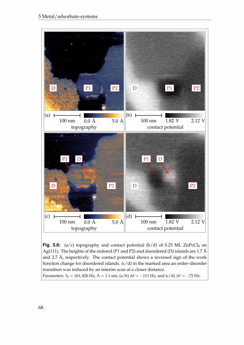
5 Metal/adsorbate-systems
D P1 P2
(a)100 nm 0.0 A 5.0 A
topography
D P1 P2
(b)100 nm 1.82 V 2.12 V
contact potential
P1 D
P2D
(c)100 nm 0.0 A 5.0 A
topography
P1 D
P2D
(d)100 nm 1.82 V 2.12 V
contact potential
Fig. 5.8: (a/c) topography and contact potential (b/d) of 0.25 ML ZnPcCl8 onAg(111). The heights of the ordered (P1 and P2) and disordered (D) islands are 1.7 Aand 2.7 A, respectively. The contact potential shows a reversed sign of the workfunction change for disordered islands. (c/d) in the marked area an order–disordertransition was induced by an interim scan at a closer distance.Parameters: f0 = 161, 826 Hz, A = 1.1 nm, (a/b) ∆f = −111 Hz, and (c/d) ∆f = −72 Hz.
68
5.2 Ag(111)/octachloro zinc phthalocyanine
(a)10 nm 0.0 A 4.0 A
topography
(b)10 nm -1.75 V -1.50 V
contact potential
P1
P2
(c)200 nm 0.0 nm 1.85 nm
topography
P1
P2
(d)200 nm -1.82 V -1.46 V
contact potential
Fig. 5.9: ZnPcCl8 adsorbed on Ag(111) in phase P1. (a) in the topography image thesingle molecules and the location of a vacancy (marked by a red circle) are visible.(b) the contact potential varies with ∆U∗dc,cor. = −(122± 50) mV corrugation alongthe molecular lattice. At the vacancy site with ∆U∗dc,mv = −(193± 53) mV a muchbrighter contrast is observed compared to the intermolecular spaces. (c/d) images(a/b) are located in the central P1 area.Parameters: f0 = 164, 249 Hz, A = 1.4 nm, (a/b) ∆f = −63 Hz, and (c/d) ∆f = −43 Hz.
69
5 Metal/adsorbate-systems
to the molecules of hmv = (1.75± 0.36) A is imaged with much brighter con-trast of ∆U∗dc,mv = −(193± 53) mV between the surrounding molecules and thevacancy site. This has to be compared to the value of ∆U∗dc,1 = −(156± 53) mVmeasured as difference6 in the contact potential for the P1 island (step heighth1 = (2.3± 0.5) A) compared to the substrate in figure 5.9d.
The footprint size of a ZnPcCl8 molecule in phase P1 estimated from the iso-density plots in [143] amounts to ≈ 2.1 nm2. With the molecular density of0.33 nm−2 the measured ∆U∗dc,mv would lead to a ∆U∗dc,1,mv = −(138± 38) mVas a simple area weighted average7, which is well in the uncertainty range of∆U∗dc,1. Therefore the higher value for the single molecules than for the islandindicates that at the vacancy site indeed a value close to the contact potentialof the substrate has been measured. Since the tip can not reach the substrate inbetween the intermolecular spaces of the lattice, already a different value com-pared to the free silver surface inside the vacancy is obtained along the molecularlattice.
With increasing distance between tip and sample surface the lateral variationvanishes until the constant value ∆U∗dc,1 is reached above the island. Interest-ingly, a direct average of the obtained contact potential map on an area of sev-eral unit cells does give a smaller value (∆U∗dc,1,av. = −(122± 46) mV) as doesthe estimate which includes the area covered by a single molecule. The rea-son is clearly that the tip already averages the potential around the edges ofthe molecule which leads to more potential values between the two extrema. Inorder to judge whether a quantitative molecular resolution can be achieved itseems therefore necessary to analyse measurements which include also largerfree sample areas as for instance vacancies in the molecular assembly.
5.3 Summary
Two examples for the adsorption of organic adsorbates on metals and the result-ing changes in the tip-sample contact potential contrast have been presented.
The initial contrast which can be observed on pristine Au(111) surfaces com-pletely vanishes after adsorption of a monolayer DB6T. This indicates a site spe-cific charge transfer or charge rearrangement in the molecular layer. The butyl
6The absolute values can not be compared due to tip changes between the single measurements.7The error estimate does not take into account any uncertainties for the footprint size of themolecule or the molecular density.
70
5.3 Summary
side chains lead to a much lower molecular density as compared to α-6T. Thisevokes the idea that a work function tuning should be possible when differentalkyl side chains are used as the electronic properties of the core thiophene arenot altered by the alkyl groups.
The correlation between different structural phases of ZnPcCl8 adsorbed onAg(111) and the contact potential difference measured in Kelvin probe forcemicroscopy was studied. The main difference between phases P1 to P3 is themolecular density caused by the formation of intermolecular hydrogen-chlorinebonds. Due to charge transfer between the silver substrate and the molecules acharge transfer dipole density builds up, which leads to differences in the con-tact potential between those phases. The push back effect varies only slightly ifat all for phases P1 and P2.
The situation happens to be changed for the newly described phase P4. There,an additional molecular dipole or a decreased push back effect leads to a hugeshift of the contact potential towards a higher work function compared to phasesP1 and P2. Finally, disordered molecular assemblies cause a contact potentialwhich lies in between the values for phase P4 and the other ordered phases.
A work function increase by 270 meV upon adsorption of the first 2 A ZnPcCl8was reported by photoelectron spectroscopy [144]. In this work, the work func-tion has been found decreased for all ordered phases P1 to P3 but increasedfor disordered areas and phase P4. A macroscopic technique like photoelectronspectroscopy will clearly measure an averaged value if a certain distribution ofdifferent phases is present. Still, a domination by phase P4 or disordered areas isquite unlikely and can thus not explain the discrepancy between the macroscopicphotoelectron spectroscopy studies and the microscopic study shown here. Pre-sumably, oxidation of the free silver surface raised the substrate work function.As a consequence, potential difference values measured between the molecu-lar layers and the substrate have been noticed to vary between different experi-ments and are therefore not representative.
Molecular resolution was shown for a ZnPcCl8 layer in phase P1. The mea-sured difference of the contact potential between a vacancy and the moleculesis larger than the value measured between a huge island and the free silver sur-face. This supports the theoretical ansatz, that the macroscopic work functionchange is given by a changed surface dipole density for monolayers of organicadsorbates also.
71

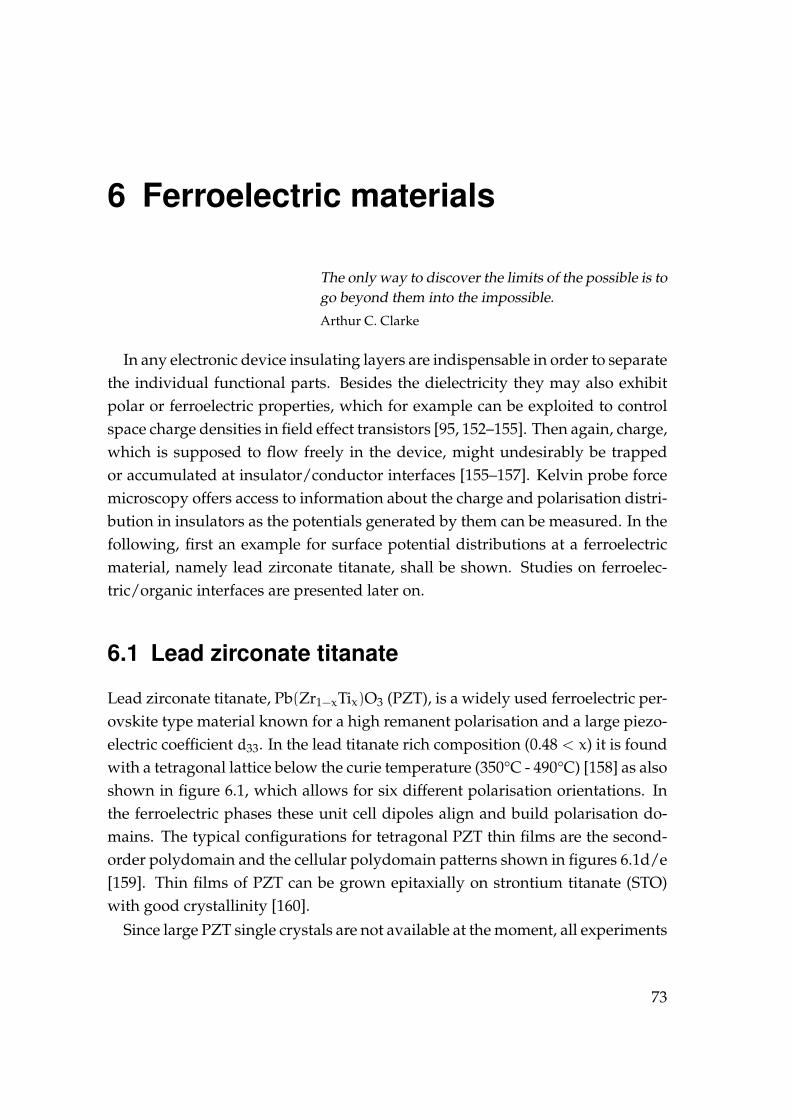
6 Ferroelectric materials
The only way to discover the limits of the possible is togo beyond them into the impossible.
Arthur C. Clarke
In any electronic device insulating layers are indispensable in order to separatethe individual functional parts. Besides the dielectricity they may also exhibitpolar or ferroelectric properties, which for example can be exploited to controlspace charge densities in field effect transistors [95, 152–155]. Then again, charge,which is supposed to flow freely in the device, might undesirably be trappedor accumulated at insulator/conductor interfaces [155–157]. Kelvin probe forcemicroscopy offers access to information about the charge and polarisation distri-bution in insulators as the potentials generated by them can be measured. In thefollowing, first an example for surface potential distributions at a ferroelectricmaterial, namely lead zirconate titanate, shall be shown. Studies on ferroelec-tric/organic interfaces are presented later on.
6.1 Lead zirconate titanate
Lead zirconate titanate, Pb(Zr1−xTix)O3 (PZT), is a widely used ferroelectric per-ovskite type material known for a high remanent polarisation and a large piezo-electric coefficient d33. In the lead titanate rich composition (0.48 < x) it is foundwith a tetragonal lattice below the curie temperature (350°C - 490°C) [158] as alsoshown in figure 6.1, which allows for six different polarisation orientations. Inthe ferroelectric phases these unit cell dipoles align and build polarisation do-mains. The typical configurations for tetragonal PZT thin films are the second-order polydomain and the cellular polydomain patterns shown in figures 6.1d/e[159]. Thin films of PZT can be grown epitaxially on strontium titanate (STO)with good crystallinity [160].
Since large PZT single crystals are not available at the moment, all experiments
73
6 Ferroelectric materials
(b)
(c)
Pb Ti/Zr O
(a)
tem
pera
ture
[°C]
0.2 0.4 0.6 0.8
100
200
300
400
PbZrO3 PbTiO3x
TC
ferroelectrictetragonal
ferroelectricrhombohedral
paraelectric cubic
anti
ferr
oele
ctri
c
(e)ax
ay
c
(d)
Fig. 6.1: (a) Simplified phase diagram of Pb(Zr1−xTix)O3 after [158]. Below thecomposition dependent Curie-temperature TC (red line) the material becomes ferro-electric or antiferroelectric for very low PbTiO3 concentration. At the morphotropicphase boundary (blue line) the structure changes between ferroelectric rhombohe-dral and ferroelectric tetragonal with eight and six possible polarisation directions,respectively. (b) Schematic drawing depicting the unit cell of Pb(Zr1−xTix)O3 in theparaelectric cubic and (b) the ferroelectric tetragonal phase. Due to the displace-ment of the central atom from the symmetry centre of the unit cell an electric dipolebuilds up. (d/e) In the ferroelectric phases the unit cell dipoles align to their neigh-bours and polarisation domains build up. The typical configurations for tetragonalPZT thin films are (d) the second-order polydomain and (e) the cellular polydomainpatterns.
74
6.1 Lead zirconate titanate
were performed with epitaxially grown Pb(Zr0.2Ti0.8)O3 thin films on 1at%-Nbdoped STO1.
For comparison a few samples grown on SRO buffered STO2 substrates wereavailable. The main difference is the lattice mismatch between the thin film andthe substrate which induces an intrinsic compressive strain of the thin film’slattice, and which is smaller in the case of SRO buffered STO [161]. It is knownthat strong compressive strain leads to a preferred c-axis orientation [162], whichmeans that the polarisation vector lies perpendicular to the surface. The polari-sation directions parallel to the surface are called ax and ay.
Sample preparation
Epitaxially grown PZT thin films exhibit a quite individual surface morphologyand surface potential distribution. Both are influenced not only by the sampleparameters, like substrate and film thickness, but also by the sample preparationprior to the measurement – especially the cleaning process. Different cleaningprocedures have been tried out and are explained in the following.
The simplest “cleaning” procedure is to leave the thin film in the as-receivedstate. Then surely the surface will be covered with adsorbate, for example likewater, as screening of the ferroelectric polarisation decreases the free energy ofthe crystal. Also, chemical bonding sites at the oxide surface will stay passivated.
The standard cleaning procedure starts with four to six washings in an ul-trasonic bath with alternating non-polar (toluene) and polar (acetone, ethanol,methanol, isopropanol) solvents. After the last bath the samples are dried in astream of nitrogen and subsequently illuminated with ultraviolet light in ambi-ent conditions in order to create an ozone atmosphere. The ozone oxidises anyremaining organic material on the sample surface and activates chemical bond-ing sites.
Unfortunately, the standard procedure turned out to be counterproductive insome cases. The reason is, that the manufacturer has to apply a conductive paste,which contains small flakes of metal (presumably silver), at the substrates back-side during the growth process [163]. Remains of this paste can go into solutionin the polar bath and consequently deposit on the ferroelectric thin film side. An
1Obtained from Phasis Sarl (www.phasis.ch) with film thicknesses of 20 nm, 50 nm, and 100 nm.The niobium doping induces conductivity of the STO substrate.
2Kindly provided by Dr. Jan Seidel, CONCEPT Research Group, UC Berkeley. Doping of theSTO is needless since SRO is already metallic.
75
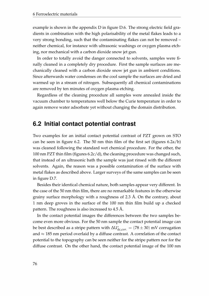
6 Ferroelectric materials
example is shown in the appendix D in figure D.6. The strong electric field gra-dients in combination with the high polarisability of the metal flakes leads to avery strong bonding, such that the contaminating flakes can not be removed –neither chemical, for instance with ultrasonic washings or oxygen plasma etch-ing, nor mechanical with a carbon dioxide snow jet gun.
In order to totally avoid the danger connected to solvents, samples were fi-nally cleaned in a completely dry procedure. First the sample surfaces are me-chanically cleaned with a carbon dioxide snow jet gun in ambient conditions.Since afterwards water condenses on the cool sample the surfaces are dried andwarmed up in a stream of nitrogen. Subsequently all chemical contaminationsare removed by ten minutes of oxygen plasma etching.
Regardless of the cleaning procedure all samples were annealed inside thevacuum chamber to temperatures well below the Curie temperature in order toagain remove water adsorbate yet without changing the domain distribution.
6.2 Initial contact potential contrast
Two examples for an initial contact potential contrast of PZT grown on STOcan be seen in figure 6.2. The 50 nm thin film of the first set (figures 6.2a/b)was cleaned following the standard wet chemical procedure. For the other, the100 nm PZT thin film (figures 6.2c/d), the cleaning procedure was changed such,that instead of an ultrasonic bath the sample was just rinsed with the differentsolvents. Again, the reason was a possible contamination of the surface withmetal flakes as described above. Larger surveys of the same samples can be seenin figure D.7.
Besides their identical chemical nature, both samples appear very different. Inthe case of the 50 nm thin film, there are no remarkable features in the otherwisegrainy surface morphology with a roughness of 2.3 A. On the contrary, about1 nm deep groves in the surface of the 100 nm thin film build up a checkedpattern. The roughness is also increased to 4.5 A.
In the contact potential images the differences between the two samples be-come even more obvious. For the 50 nm sample the contact potential image canbe best described as a stripe pattern with ∆U∗dc,cor. = (78± 30) mV corrugationand ≈ 185 nm period overlaid by a diffuse contrast. A correlation of the contactpotential to the topography can be seen neither for the stripe pattern nor for thediffuse contrast. On the other hand, the contact potential image of the 100 nm
76
6.2 Initial contact potential contrast
(a)500 nm 0.0 nm 1.6 nm
topography
(b)500 nm 1.9 V 2.5 V
contact potential
(c)250 nm 0.0 nm 3.7 nm
topography
(d)250 nm -2.6 V -0.3 V
contact potential
Fig. 6.2: (a/b) 50 nm and (c/d) 100 nm PZT thin film on STO. Both cleaned with awet chemical procedure. Please see text on page 76 for details.Parameters: (a/b) f0 = 164, 409 Hz, A = 1.5 nm, ∆f = −30 Hz, T = 81 K.(c/d) f0 = 55, 405 Hz, A = 6.0 nm, ∆f = −57 Hz, T = 81 K.
77
6 Ferroelectric materials
sample is governed by a checked pattern with peak-to-valley contrast of up to1.6 V, which now is clearly related to the surface topography. Also, no diffusecontrast is visible, which can be explained with the very large contrast rangecompared to the 50 nm sample.
In order to further understand the observations the impact of the cleaningprocedures has been studied. In figure 6.3 a comparison between the surfacemorphology and the contact potential of two 20 nm PZT thin film twin – cutfrom the same masterpiece – in the as-received state (a/b) and after the full drycleaning procedure (c/d) is made. Larger surveys of the same samples can beseen in the appendix D in figure D.8.
A notable change occurs in both surface morphology and contact potential.In the as-received state a diffuse contrast dominates the images. Only in thetopography image an underlying stripe pattern can be seen. After the cleaningthe surface morphology is dominated by small cavities, which are imaged withup to 4 nm in depth. Correlated to these cavities, also the contact potentialchanges by about ≈ 400 mV, while the diffuse contrast has mostly vanished.
Complementary to the microscopic investigations, X-ray photoelectron spec-troscopy (XPS) has been used to study the impact of the cleaning procedure. Theresults can be summarised with the two surveys shown in figure 6.4. There, thesame sample is compared in the as-received state and after the full wet chemicalprocedure. As expected, the carbon peak, which indicates contamination of thesample with organic material, is significantly reduced after the cleaning. The rel-atively small increase of the lead- and oxygen peaks is naturally induced by thereduction of the organic contaminant. Otherwise no changes in the XPS-spectraare visible, which implies that the PZT thin film itself is not modified. This is ofcourse expected as an oxide should not further react with an ozone atmosphereor an oxygen plasma.
In the light of this result the disappearance of the diffuse contact potentialcontrast and the sharpening of the surface morphology in figure 6.3 from theas-received to the cleaned state can be understood as a reduction of contami-nant coverage. Therewith, also the screening charge distribution becomes moreuniform. Similarly, the diffuse contact potential distribution in figure 6.2b canbe explained by screening charge. In comparison of figure 6.2b and figure 6.3dthe oxygen plasma etching in the dry cleaning procedure removes the contami-
78
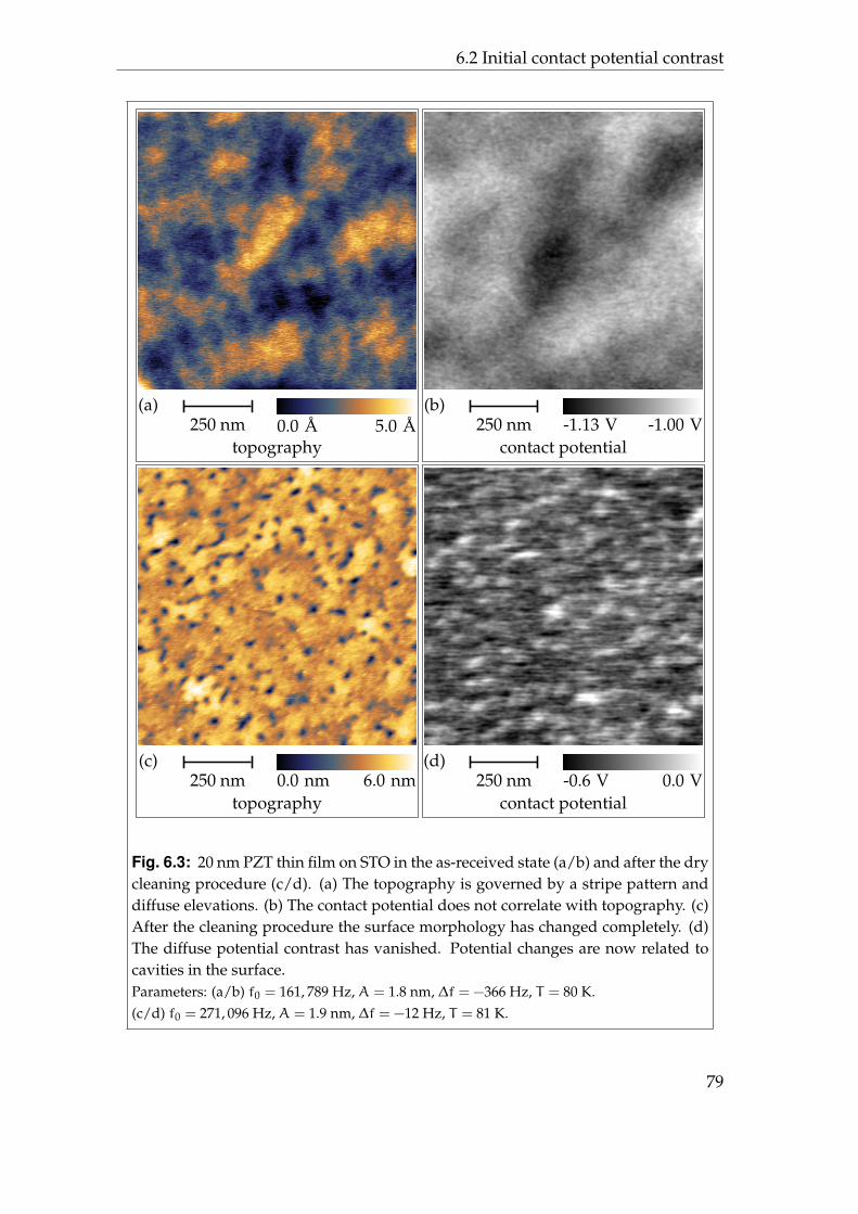
6.2 Initial contact potential contrast
(a)250 nm 0.0 A 5.0 A
topography
(b)250 nm -1.13 V -1.00 V
contact potential
(c)250 nm 0.0 nm 6.0 nm
topography
(d)250 nm -0.6 V 0.0 V
contact potential
Fig. 6.3: 20 nm PZT thin film on STO in the as-received state (a/b) and after the drycleaning procedure (c/d). (a) The topography is governed by a stripe pattern anddiffuse elevations. (b) The contact potential does not correlate with topography. (c)After the cleaning procedure the surface morphology has changed completely. (d)The diffuse potential contrast has vanished. Potential changes are now related tocavities in the surface.Parameters: (a/b) f0 = 161, 789 Hz, A = 1.8 nm, ∆f = −366 Hz, T = 80 K.(c/d) f0 = 271, 096 Hz, A = 1.9 nm, ∆f = −12 Hz, T = 81 K.
79
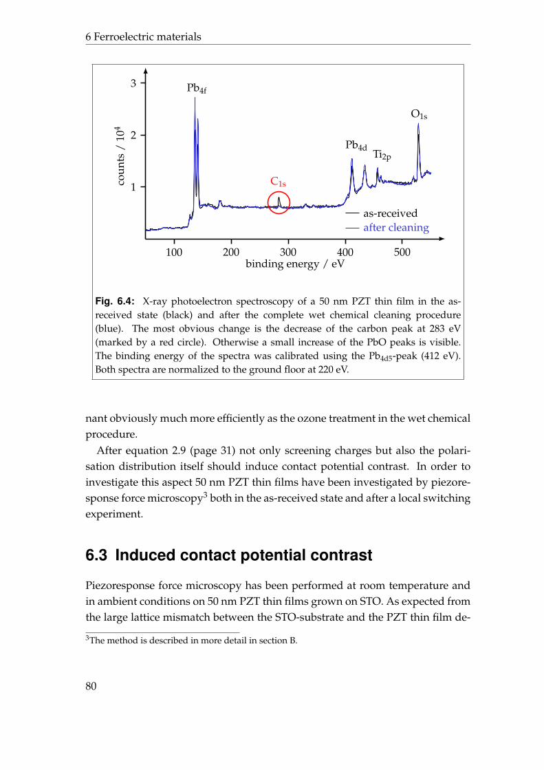
6 Ferroelectric materials
as-receivedafter cleaning
binding energy / eV
coun
ts/
104
1
2
3
100 200 300 400 500
Pb4f
Pb4dTi2p
O1s
C1s
Fig. 6.4: X-ray photoelectron spectroscopy of a 50 nm PZT thin film in the as-received state (black) and after the complete wet chemical cleaning procedure(blue). The most obvious change is the decrease of the carbon peak at 283 eV(marked by a red circle). Otherwise a small increase of the PbO peaks is visible.The binding energy of the spectra was calibrated using the Pb4d5-peak (412 eV).Both spectra are normalized to the ground floor at 220 eV.
nant obviously much more efficiently as the ozone treatment in the wet chemicalprocedure.
After equation 2.9 (page 31) not only screening charges but also the polari-sation distribution itself should induce contact potential contrast. In order toinvestigate this aspect 50 nm PZT thin films have been investigated by piezore-sponse force microscopy3 both in the as-received state and after a local switchingexperiment.
6.3 Induced contact potential contrast
Piezoresponse force microscopy has been performed at room temperature andin ambient conditions on 50 nm PZT thin films grown on STO. As expected fromthe large lattice mismatch between the STO-substrate and the PZT thin film de-
3The method is described in more detail in section B.
80
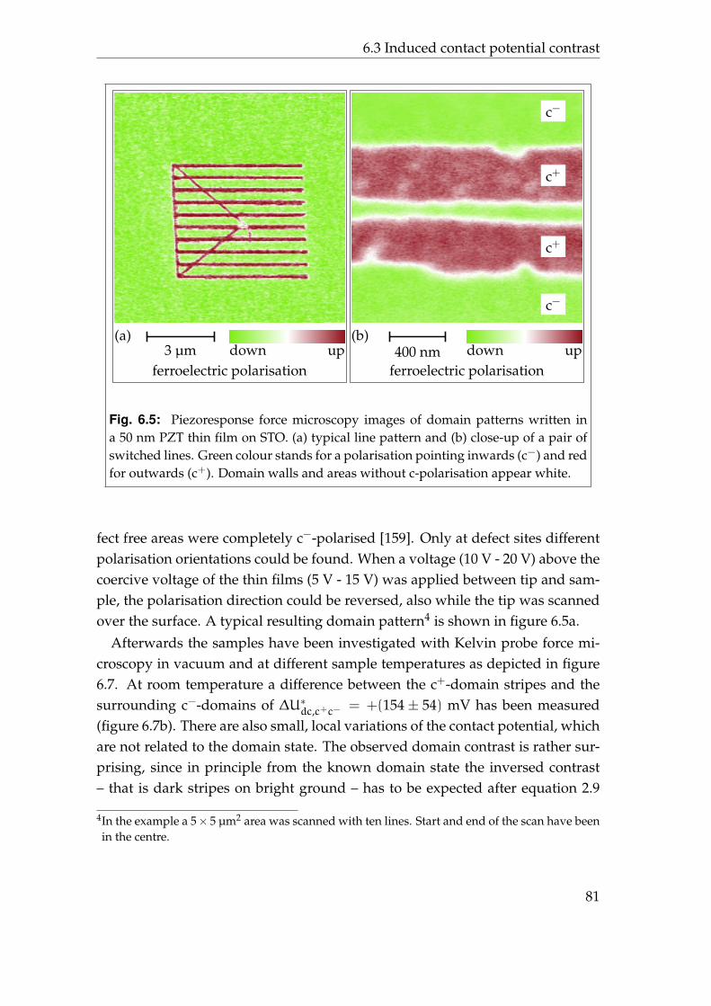
6.3 Induced contact potential contrast
(a)3 µm down up
ferroelectric polarisation
c−
c+
c+
c−
(b)400 nm down up
ferroelectric polarisation
Fig. 6.5: Piezoresponse force microscopy images of domain patterns written ina 50 nm PZT thin film on STO. (a) typical line pattern and (b) close-up of a pair ofswitched lines. Green colour stands for a polarisation pointing inwards (c−) and redfor outwards (c+). Domain walls and areas without c-polarisation appear white.
fect free areas were completely c−-polarised [159]. Only at defect sites differentpolarisation orientations could be found. When a voltage (10 V - 20 V) above thecoercive voltage of the thin films (5 V - 15 V) was applied between tip and sam-ple, the polarisation direction could be reversed, also while the tip was scannedover the surface. A typical resulting domain pattern4 is shown in figure 6.5a.
Afterwards the samples have been investigated with Kelvin probe force mi-croscopy in vacuum and at different sample temperatures as depicted in figure6.7. At room temperature a difference between the c+-domain stripes and thesurrounding c−-domains of ∆U∗dc,c+c− = +(154 ± 54) mV has been measured(figure 6.7b). There are also small, local variations of the contact potential, whichare not related to the domain state. The observed domain contrast is rather sur-prising, since in principle from the known domain state the inversed contrast– that is dark stripes on bright ground – has to be expected after equation 2.9
4In the example a 5× 5 µm2 area was scanned with ten lines. Start and end of the scan have beenin the centre.
81
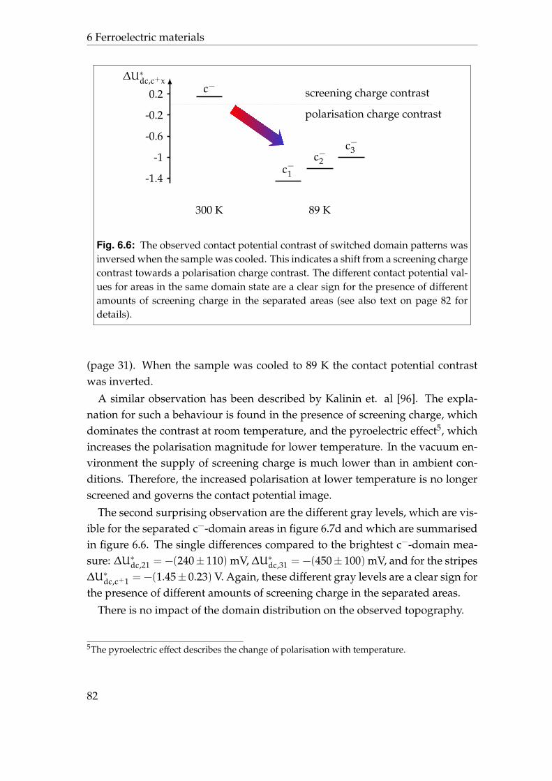
6 Ferroelectric materials
∆U∗dc,c+xc−
c−3c−2
c−1
0.2
-0.2
-0.6
-1
-1.4
300 K 89 K
screening charge contrast
polarisation charge contrast
Fig. 6.6: The observed contact potential contrast of switched domain patterns wasinversed when the sample was cooled. This indicates a shift from a screening chargecontrast towards a polarisation charge contrast. The different contact potential val-ues for areas in the same domain state are a clear sign for the presence of differentamounts of screening charge in the separated areas (see also text on page 82 fordetails).
(page 31). When the sample was cooled to 89 K the contact potential contrastwas inverted.
A similar observation has been described by Kalinin et. al [96]. The expla-nation for such a behaviour is found in the presence of screening charge, whichdominates the contrast at room temperature, and the pyroelectric effect5, whichincreases the polarisation magnitude for lower temperature. In the vacuum en-vironment the supply of screening charge is much lower than in ambient con-ditions. Therefore, the increased polarisation at lower temperature is no longerscreened and governs the contact potential image.
The second surprising observation are the different gray levels, which are vis-ible for the separated c−-domain areas in figure 6.7d and which are summarisedin figure 6.6. The single differences compared to the brightest c−-domain mea-sure: ∆U∗dc,21 = −(240± 110) mV, ∆U∗dc,31 = −(450± 100) mV, and for the stripes∆U∗dc,c+1 = −(1.45± 0.23) V. Again, these different gray levels are a clear sign forthe presence of different amounts of screening charge in the separated areas.
There is no impact of the domain distribution on the observed topography.
5The pyroelectric effect describes the change of polarisation with temperature.
82
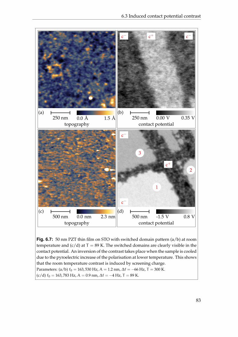
6.3 Induced contact potential contrast
(a)250 nm 0.0 A 1.5 A
topography
c− c+ c−
(b)250 nm 0.00 V 0.35 V
contact potential
(c)500 nm 0.0 nm 2.3 nm
topography
c−
c+
c−
1
2
3
(d)500 nm -1.5 V 0.8 V
contact potential
Fig. 6.7: 50 nm PZT thin film on STO with switched domain pattern (a/b) at roomtemperature and (c/d) at T = 89 K. The switched domains are clearly visible in thecontact potential. An inversion of the contrast takes place when the sample is cooleddue to the pyroelectric increase of the polarisation at lower temperature. This showsthat the room temperature contrast is induced by screening charge.Parameters: (a/b) f0 = 163, 530 Hz, A = 1.2 nm, ∆f = −66 Hz, T = 300 K.(c/d) f0 = 163, 783 Hz, A = 0.9 nm, ∆f = −4 Hz, T = 89 K.
83
6 Ferroelectric materials
Typical pyroelectric coefficients for epitaxially grown Pb(Zr0.2Ti0.8)O3 thinfilms lie in the range of γ = 3 · 10−2 . . . 2 · 10−1 µC/cm2K [164]. With the ap-plied temperature change of 210 K the pyroelectric increase of the polarisationamounts to ≈ 6 · · · 40 µC/cm2. The maximum contrast change between roomtemperature and 89 K was measured to
∆U∗dc,c+c−(89K) −∆U∗dc,c+c−(300K) = −(1.60± 0.77) V.
With a sample thickness of df = 50 nm the dielectric constant of the PZT thinfilm is determined after equation 2.9 as ε ≈ 400 . . . 2800. These values are muchlarger than the expected range of ε = 30 . . . 40 for Pb(Zr0.2Ti0.8)O3 thin films[165]. Using equation 2.96, this can only be explained with the presence of ascreening charge σs ≈ 5.5 · · · 39.5 µC/cm2.
One source for such a screening charge might be conductive channels throughthe thin film. In experiments with large scale electrodes, these were in manycases short circuited to the back electrode, which indicates the existence of suchchannels. Surface conductivity – as has been reported for ferroelectric bariumtitanate [166] – would dispense screening charges from these channels over thesurface. The very uniform contact potential distribution inside the areas withdifferent contact potential level, which are divided by the c+-domain stripes,yields a further argument for the described scenario.
From the above mentioned experiments three conclusions can be drawn:
1. Polarisation contrast at low temperatures emerges due to the pyroelectricproperties of the ferroelectric samples. Therefore it is not directly7 con-nected to the magnitude of the remanent polarisation.
2. Local contact potential variations up to a few hundred millivolt can occurdue to a non-uniform screening charge distribution.
3. There is no influence of the switched domain distribution on the surfacetopography.
Going back to figure 6.3c/d, the contrast related to the cavities is most proba-bly not induced by a polarisation reversal, but instead by the topography itself– either due to a local charge distribution or as an experimental artefact. The
6Again it has to be noted, that equation 2.9 can serve only as rough approximation of the problemsince d · ε−1 is already considerable large compared to the closest tip sample distance.
7It still might be connected indirectly due to the amount of screening charge.
84
6.4 Summary
same could be the case for the 100 nm thin film in figure 6.2c/d. Yet, the contrastmagnitude observed there indicates a polarisation driven contrast. In addition,it is known from less strained thin films that usually the cellular polydomainpolarisation pattern evolves where thin a-domains separate larger c-domains.Examples are PZT films grown on a SRO buffered STO substrates8 [167], or thinfilms which are thick enough, such that a relaxation of the misfit strain can takeplace [159, 168, 169]. The striking similarity of the patterns leads to the conclu-sion, that in the case of the 100 nm PZT (figure 6.2c/d) thin film already the morecomplex cellular polydomain distribution evolved. Similarly, the stripe patternof the 50 nm PZT (figure 6.2a/b) thin film might be related to the second-orderpolydomain pattern.
6.4 Summary
Epitaxially grown Pb(Zr0.2Ti0.8)O3 thin films with various thicknesses on nio-bium doped strontium titanate have been investigated with Kelvin probe forcemicroscopy, also at low temperature. A great variety of sample properties hasbeen found. The observed contact potential contrast originates both in thescreening charge distribution and the ferroelectric polarisation distribution, aswas expected. The latter is naturally screened. Pyroelectric effects induce a po-larisation charge contrast after a temperature change.
Thin films of 20 nm and 50 nm were found in a unipolar domain state inducedby the misfit strain of the substrate. Contact potential variations are connectedto an uneven screening charge distribution and topographic features. Cellularpolydomain distributions with alternating a- and c-domains evolved in 100 nmthin films. While intentionally switched domain patterns leave the sample to-pography unchanged, a correlation between topography and domain pattern isobserved for naturally evolved domain states.
Kelvin probe force microscopy can clearly help to visualise domain distribu-tions in ferroelectric samples. But, due to the very complex electrostatic proper-ties of these materials, a quantitative analysis of the observed contact potentialdistributions becomes impossible. Nevertheless a compensation of electrostaticforces like in Kelvin probe force microscopy is mandatory for non-contact atomicforce microscopy studies since the variations of the contact potential reach mag-nitudes of several volts.
8As for instance shown in figure D.9 in the appendix D.
85

7 Ferroelectric/organic-systems
I have yet to see any problem, however complicated,which, when you looked at it in the right way, did notbecome still more complicated.
Poul Anderson
The investigation of ferroelectric/organic-systems has attracted interest inthe past years [155]. The high dielectric constants and the remanent polarisa-tion of ferroelectric materials might be useful for organic field effect transistors[154, 170] or pyroelectric sensors [171]. Of course inorganic ferroelectrics, like forinstance lead zirconate titanate, are rarely compatible with the objective targetsof organic electronics as they need high processing temperatures, rigid and crys-talline substrates, and are quite expensive if a good quality is demanded. On theother hand, organic electronics shall be cheap, easily processable and mechani-cally flexible [172, 173].
Nevertheless, the research especially on the ferroelectric transistor as a non-volatile and non-destructive read-out memory device has not come to a completeand profound solution for the design of such memory devices [174]. From thispoint of view further investigations of high quality inorganic ferroelectrics alsofor organic electronics can of benefit.
Here, epitaxially grown lead zirconate titanate (PZT) thin films, as presentedin the previous section, are used as substrate for two different molecular species.
The first is a classical self assembly molecule, namely 5-cyano-2-(butyl-4-phosphonic acid)-3-butylthiophene (CnBtPA), as a prototype for these kind ofspecifically designed functional materials.
In contrast, the α,ω-dicyano substituted-β,β′-dibutyl quaterthiophene (DC-nDB4T) happens to be an example for a typical small molecule organic semicon-ductor. Thin films of both organic materials on PZT have been investigated withKelvin probe force microscopy. In the following, first results on PZT/CnBtPAand afterwards of PZT/DCnDB4T as well as PZT/CnBtPA/DCnDB4T areshown.
87
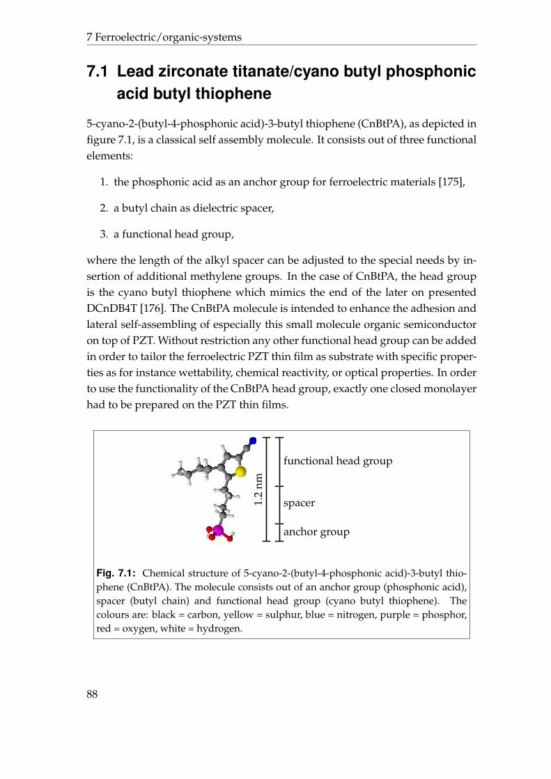
7 Ferroelectric/organic-systems
7.1 Lead zirconate titanate/cyano butyl phosphonicacid butyl thiophene
5-cyano-2-(butyl-4-phosphonic acid)-3-butyl thiophene (CnBtPA), as depicted infigure 7.1, is a classical self assembly molecule. It consists out of three functionalelements:
1. the phosphonic acid as an anchor group for ferroelectric materials [175],
2. a butyl chain as dielectric spacer,
3. a functional head group,
where the length of the alkyl spacer can be adjusted to the special needs by in-sertion of additional methylene groups. In the case of CnBtPA, the head groupis the cyano butyl thiophene which mimics the end of the later on presentedDCnDB4T [176]. The CnBtPA molecule is intended to enhance the adhesion andlateral self-assembling of especially this small molecule organic semiconductoron top of PZT. Without restriction any other functional head group can be addedin order to tailor the ferroelectric PZT thin film as substrate with specific proper-ties as for instance wettability, chemical reactivity, or optical properties. In orderto use the functionality of the CnBtPA head group, exactly one closed monolayerhad to be prepared on the PZT thin films.
1.2
nm
anchor group
spacer
functional head group
Fig. 7.1: Chemical structure of 5-cyano-2-(butyl-4-phosphonic acid)-3-butyl thio-phene (CnBtPA). The molecule consists out of an anchor group (phosphonic acid),spacer (butyl chain) and functional head group (cyano butyl thiophene). Thecolours are: black = carbon, yellow = sulphur, blue = nitrogen, purple = phosphor,red = oxygen, white = hydrogen.
88
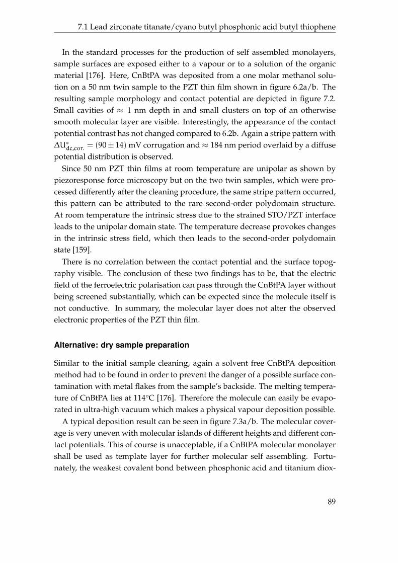
7.1 Lead zirconate titanate/cyano butyl phosphonic acid butyl thiophene
In the standard processes for the production of self assembled monolayers,sample surfaces are exposed either to a vapour or to a solution of the organicmaterial [176]. Here, CnBtPA was deposited from a one molar methanol solu-tion on a 50 nm twin sample to the PZT thin film shown in figure 6.2a/b. Theresulting sample morphology and contact potential are depicted in figure 7.2.Small cavities of ≈ 1 nm depth in and small clusters on top of an otherwisesmooth molecular layer are visible. Interestingly, the appearance of the contactpotential contrast has not changed compared to 6.2b. Again a stripe pattern with∆U∗dc,cor. = (90± 14) mV corrugation and ≈ 184 nm period overlaid by a diffusepotential distribution is observed.
Since 50 nm PZT thin films at room temperature are unipolar as shown bypiezoresponse force microscopy but on the two twin samples, which were pro-cessed differently after the cleaning procedure, the same stripe pattern occurred,this pattern can be attributed to the rare second-order polydomain structure.At room temperature the intrinsic stress due to the strained STO/PZT interfaceleads to the unipolar domain state. The temperature decrease provokes changesin the intrinsic stress field, which then leads to the second-order polydomainstate [159].
There is no correlation between the contact potential and the surface topog-raphy visible. The conclusion of these two findings has to be, that the electricfield of the ferroelectric polarisation can pass through the CnBtPA layer withoutbeing screened substantially, which can be expected since the molecule itself isnot conductive. In summary, the molecular layer does not alter the observedelectronic properties of the PZT thin film.
Alternative: dry sample preparation
Similar to the initial sample cleaning, again a solvent free CnBtPA depositionmethod had to be found in order to prevent the danger of a possible surface con-tamination with metal flakes from the sample’s backside. The melting tempera-ture of CnBtPA lies at 114°C [176]. Therefore the molecule can easily be evapo-rated in ultra-high vacuum which makes a physical vapour deposition possible.
A typical deposition result can be seen in figure 7.3a/b. The molecular cover-age is very uneven with molecular islands of different heights and different con-tact potentials. This of course is unacceptable, if a CnBtPA molecular monolayershall be used as template layer for further molecular self assembling. Fortu-nately, the weakest covalent bond between phosphonic acid and titanium diox-
89
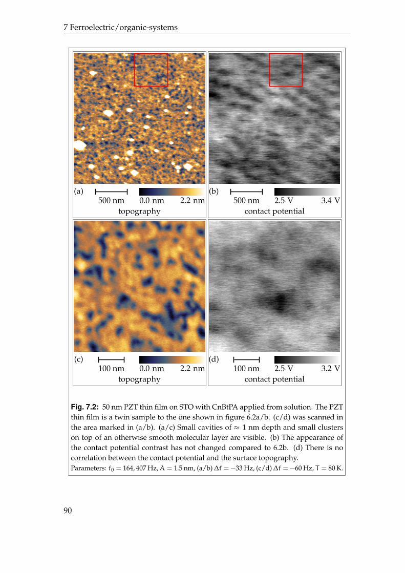
7 Ferroelectric/organic-systems
(a)500 nm 0.0 nm 2.2 nm
topography
(b)500 nm 2.5 V 3.4 V
contact potential
(c)100 nm 0.0 nm 2.2 nm
topography
(d)100 nm 2.5 V 3.2 V
contact potential
Fig. 7.2: 50 nm PZT thin film on STO with CnBtPA applied from solution. The PZTthin film is a twin sample to the one shown in figure 6.2a/b. (c/d) was scanned inthe area marked in (a/b). (a/c) Small cavities of ≈ 1 nm depth and small clusterson top of an otherwise smooth molecular layer are visible. (b) The appearance ofthe contact potential contrast has not changed compared to 6.2b. (d) There is nocorrelation between the contact potential and the surface topography.Parameters: f0 = 164, 407 Hz,A = 1.5 nm, (a/b)∆f = −33 Hz, (c/d)∆f = −60 Hz, T = 80 K.
90
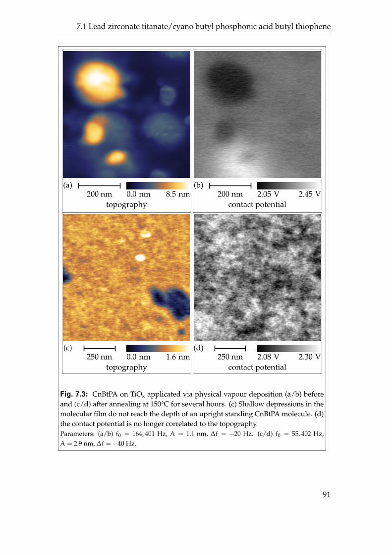
7.1 Lead zirconate titanate/cyano butyl phosphonic acid butyl thiophene
(a)200 nm 0.0 nm 8.5 nm
topography
(b)200 nm 2.05 V 2.45 V
contact potential
(c)250 nm 0.0 nm 1.6 nm
topography
(d)250 nm 2.08 V 2.30 V
contact potential
Fig. 7.3: CnBtPA on TiOx applicated via physical vapour deposition (a/b) beforeand (c/d) after annealing at 150°C for several hours. (c) Shallow depressions in themolecular film do not reach the depth of an upright standing CnBtPA molecule. (d)the contact potential is no longer correlated to the topography.Parameters: (a/b) f0 = 164, 401 Hz, A = 1.1 nm, ∆f = −20 Hz. (c/d) f0 = 55, 402 Hz,A = 2.9 nm, ∆f = −40 Hz.
91
7 Ferroelectric/organic-systems
binding energy / eV
coun
ts/
104
0.5
1
1.5
2
2.5
100 200 300 400 500
S2s C1s N1s
O1s
Ti2p
P2p S2p
Fig. 7.4: X-ray photoelectron spectrum of the TiOx/CnBtPA-sample shown in fig-ure 7.3. The inset shows the energy range of the P2p- and S2p-peaks (marked by thered rectangle). All elements of the CnBtPA molecule are visible (red labels). Thebinding energy of the spectrum was calibrated using the Ti2p3-peak (458 eV).
ide (TiO2) – one major ingredient of PZT – is with 1.32 eV per bond much higherthan the melting energy of 33 meV per molecule [177]. This opens up a secondway how to realise a CnBtPA monolayer coverage but now without any solventsinvolved.
First a large amount of organic material is deposited via physical vapour de-position onto the substrate1 at room temperature. Subsequently, the sampleis annealed for a sufficient time2 at a temperature above the sublimation tem-perature but well below the decomposition temperature of the molecule or anyother critical temperature as for instance the ferroelectric Curie temperature. ForCnBtPA temperatures of 150°C to 180°C were sufficient. Any material whichalready established a covalent bond to the substrate remains, while additionalmolecules are re-sublimated and leave the sample. Due to the design of theCnBtPA molecule – but of course this ansatz can easily be followed for othersubstrate-molecule combinations – a nearly perfect monolayer is left after the
1Titanium oxide was chosen as cheap replacement of PZT in the verification stadium.2Here always at least one hour.
92
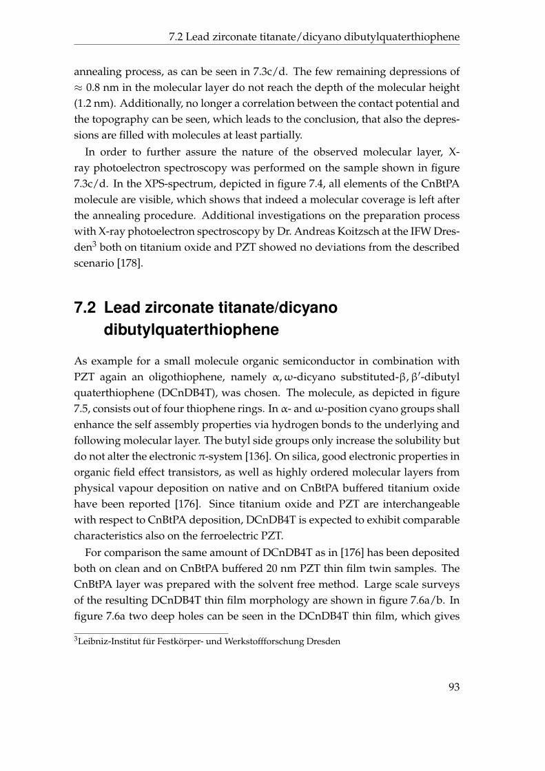
7.2 Lead zirconate titanate/dicyano dibutylquaterthiophene
annealing process, as can be seen in 7.3c/d. The few remaining depressions of≈ 0.8 nm in the molecular layer do not reach the depth of the molecular height(1.2 nm). Additionally, no longer a correlation between the contact potential andthe topography can be seen, which leads to the conclusion, that also the depres-sions are filled with molecules at least partially.
In order to further assure the nature of the observed molecular layer, X-ray photoelectron spectroscopy was performed on the sample shown in figure7.3c/d. In the XPS-spectrum, depicted in figure 7.4, all elements of the CnBtPAmolecule are visible, which shows that indeed a molecular coverage is left afterthe annealing procedure. Additional investigations on the preparation processwith X-ray photoelectron spectroscopy by Dr. Andreas Koitzsch at the IFW Dres-den3 both on titanium oxide and PZT showed no deviations from the describedscenario [178].
7.2 Lead zirconate titanate/dicyanodibutylquaterthiophene
As example for a small molecule organic semiconductor in combination withPZT again an oligothiophene, namely α,ω-dicyano substituted-β,β′-dibutylquaterthiophene (DCnDB4T), was chosen. The molecule, as depicted in figure7.5, consists out of four thiophene rings. In α- andω-position cyano groups shallenhance the self assembly properties via hydrogen bonds to the underlying andfollowing molecular layer. The butyl side groups only increase the solubility butdo not alter the electronic π-system [136]. On silica, good electronic properties inorganic field effect transistors, as well as highly ordered molecular layers fromphysical vapour deposition on native and on CnBtPA buffered titanium oxidehave been reported [176]. Since titanium oxide and PZT are interchangeablewith respect to CnBtPA deposition, DCnDB4T is expected to exhibit comparablecharacteristics also on the ferroelectric PZT.
For comparison the same amount of DCnDB4T as in [176] has been depositedboth on clean and on CnBtPA buffered 20 nm PZT thin film twin samples. TheCnBtPA layer was prepared with the solvent free method. Large scale surveysof the resulting DCnDB4T thin film morphology are shown in figure 7.6a/b. Infigure 7.6a two deep holes can be seen in the DCnDB4T thin film, which gives
3Leibniz-Institut fur Festkorper- und Werkstoffforschung Dresden
93
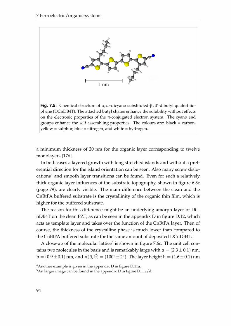
7 Ferroelectric/organic-systems
1 nm
Fig. 7.5: Chemical structure of α,ω-dicyano substituted-β,β′-dibutyl quaterthio-phene (DCnDB4T). The attached butyl chains enhance the solubility without effectson the electronic properties of the π-conjugated electron system. The cyano endgroups enhance the self assembling properties. The colours are: black = carbon,yellow = sulphur, blue = nitrogen, and white = hydrogen.
a minimum thickness of 20 nm for the organic layer corresponding to twelvemonolayers [176].
In both cases a layered growth with long stretched islands and without a pref-erential direction for the island orientation can be seen. Also many screw dislo-cations4 and smooth layer transitions can be found. Even for such a relativelythick organic layer influences of the substrate topography, shown in figure 6.3c(page 79), are clearly visible. The main difference between the clean and theCnBtPA buffered substrate is the crystallinity of the organic thin film, which ishigher for the buffered substrate.
The reason for this difference might be an underlying amorph layer of DC-nDB4T on the clean PZT, as can be seen in the appendix D in figure D.12, whichacts as template layer and takes over the function of the CnBtPA layer. Then ofcourse, the thickness of the crystalline phase is much lower than compared tothe CnBtPA buffered substrate for the same amount of deposited DCnDB4T.
A close-up of the molecular lattice5 is shown in figure 7.6c. The unit cell con-tains two molecules in the basis and is remarkably large with a = (2.3± 0.1) nm,b = (0.9± 0.1) nm, and ^(~a,~b) = (100°± 2°). The layer height h = (1.6± 0.1) nm
4Another example is given in the appendix D in figure D.11a.5An larger image can be found in the appendix D in figure D.11c/d.
94
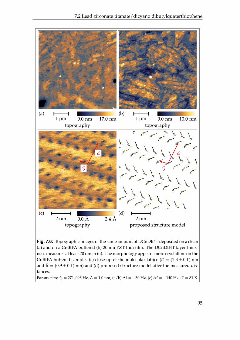
7.2 Lead zirconate titanate/dicyano dibutylquaterthiophene
(a)1 µm 0.0 nm 17.0 nm
topography
(b)1 µm 0.0 nm 10.0 nm
topography
~a
~b
(c)2 nm 0.0 A 2.4 A
topography
(d)2 nm
proposed structure model
~a
~b
Fig. 7.6: Topographic images of the same amount of DCnDB4T deposited on a clean(a) and on a CnBtPA buffered (b) 20 nm PZT thin film. The DCnDB4T layer thick-ness measures at least 20 nm in (a). The morphology appears more crystalline on theCnBtPA buffered sample. (c) close-up of the molecular lattice (~a = (2.3± 0.1) nmand ~b = (0.9± 0.1) nm) and (d) proposed structure model after the measured dis-tances.Parameters: f0 = 271, 096 Hz, A = 1.0 nm, (a/b) ∆f = −30 Hz, (c) ∆f = −140 Hz , T = 81 K.
95
7 Ferroelectric/organic-systems
(a)100 nm 0.0 nm 5.0 nm
topography
(b)100 nm -0.6 V -0.1 V
contact potential
(c)4 nm 0.0 A 2.0 A
topography
(d)5 nm 0.0 A 1.2 A
topography
Fig. 7.7: Phase boundaries in DCnDB4T layers. While the organic thin films arecharacterised by large islands, these islands are divided in smaller areas with dif-ferent molecular orientation. (a) Orientational domain boundaries occur within thesingle island layers (red arrows) and at dislocation sites, as for instance screw dis-locations (red circle), (b) without any impact on the contact potential. The higherresolved images of such boundaries are taken at (c) a boundary between two do-mains inside one island and (d) a boundary at the smooth end of an island.Parameters: f0 = 271, 096 Hz, A = 1.0 nm, (a/b) ∆f = −40 Hz, (c) ∆f = −270 Hz, (d)∆f = −310 Hz, T = 81 K.
96
7.3 Summary
was measured at the full step height side of the islands. Along the molecularrows always the two neighbouring molecules are tilted ≈ 50°towards the rowaxis ~b. The existence of such molecular rows naturally explains the observedstretched island morphology.Apparently, there is no preferential direction forthe growth of these rows.
Naturally, the random island orientation distribution and both the numerousscrew dislocations as well as the smooth layer transitions cause many bound-aries between domains with different molecular row orientation. A few exam-ples are depicted in figure 7.7. In the higher resolved images in figure 7.7c/dmany defects around the boundaries and a considerable huge gap at the bound-ary itself can be seen. From the prototypic α-sexithiophene (α-6T) it is known,that similar grain boundaries significantly increase the organic layer resistance[110]. A reduction of such boundaries would therefore be beneficial for the elec-tronic properties of the DCnDB4T thin films.
The contact potential distribution in figure 7.7b is independent from the thinfilm topography. Yet, still a diffuse contrast can be seen6. Again the contrastequals the image known from the clean PZT surface, figure 6.3d (page 79). Asin the case of CnBtPA the reason has to be seen in the pyroelectric increase ofthe ferroelectric polarisation which is not screened by the molecular layer. Fora semiconducting material screening of the electric fields induced by the ferro-electric polarisation is expected at room temperature and would exactly be thedesired effect in a ferroelectric organic field effect transistor. Yet, at low temper-atures semiconductors behave more like insulators and thus the electric fieldsdue to the pyroelectric effect are not screened.
7.3 Summary
Deposition, growth and electronic properties of two different organic materialson epitaxially grown PZT thin films have been investigated.
The self assembly molecule CnBtPA was found to be functional as templatemolecule for the ordered growth of subsequent semiconducting DCnDB4T lay-ers. Besides the standard wet chemical application of a CnBtPA monolayer fromsolution, an alternative dry deposition procedure was established. This allows tocircumvent any wet process in the preparation of PZT thin films and in principlealso in vacua processing of ferroelectric organic field effect transistors.
6Another example is shown in the appendix D in figure D.11a/b.
97
7 Ferroelectric/organic-systems
CnBtPA sub-monolayer coverage has no impact on the contact potential dis-tribution of PZT thin films at low temperature. Due to the insulating propertiesof the molecule no screening of the electric fields of the ferroelectric polarisationoccurs.
Similar electronic behaviour is found for DCnDB4T layers both on top of cleanas well as CnBtPA buffered PZT thin films. Clearly the conductance of the molec-ular layer drops with temperature while due to the pyroelectric effect the polar-isation increases simultaneously. Therefore, below a certain temperature againthe electric fields are no longer screened.
DCnDB4T shows a well ordered self assembling on both kinds of substrate,while in the case of the CnBtPA buffered PZT the thin film crystallinity is en-hanced. Due to a lack of preferential order many orientational domains arise.The domain boundaries are characterised by many crystal defects and huge in-termolecular distances between neighbouring domains. This is disadvantageousfor electrical conductance.
High resolution images revealed a molecular lattice close to the values knownin literature from titanium oxide substrates.
98
8 Conclusion
Dreams, goals, ambitions - these are the stuff man usesfor fuel.L. Ron Hubbard
8.1 Synopsis
In this work the question after the origin of contrast in Kelvin probe force mi-croscopy has been addressed.
The general hypothesis, that a lateral variation of a multi-polar differentialcharge density at the surface of the conductive sample leads to the observablecontrast, allows for three predictions. Firstly, lateral contact potential contrastshould exist even on bare metal surfaces, if the surface is reconstructed or ex-hibits deviations from the perfect crystal structure, such as defects or steps. Sec-ondly, a simple correspondence between the surface dipole density of larger ar-eas and the contact potential difference above them should be found. Finally, thesame should apply for insulating adsorbates with high dielectric constant, if theeffective adsorbate thickness df/ε is smaller than the tip sample distance.
These predictions have been tested and verified on a number of different sam-ple systems. The single experimental findings are as follows:
• It has been shown, that defects, step edges, and the herringbone surfacereconstruction on Au(111) surfaces lead to contrast in the contact potential.For the first time these local potentials have been visualized in a direct wayin the case of the Au(111)-(22×
√3) reconstruction.
• One so far unreported type of Au(111) surface reconstruction morphologyhas been found. Scanning tunnelling microscopy revealed that these mor-phology corresponds to Au(111)-(22×
√3) reconstruction networks. The
large contact potential contrast is an expression of the energetically unbal-anced surface state.
99
8 Conclusion
• The difference in the contact potential between two structural phases ofoctachloro zinc phthalocyanine on Ag(111) have been quantitatively ex-plained with the help of the differential charge density model. The truemolecular contrast of one of these phases could be explained the same way.
• For the first time a structural phase of octachloro zinc phthalocyanine onAg(111) with wide open molecular lattice and a huge difference in the con-tact potential compared to all so far known phases has been visualized anddescribed.
• Polarisation domain patterns in lead zirconate titanate thin films have beenvisualised. The observed contact potential contrast has been found to bedominated by screening charge at room temperature. Pyroelectric effectsinduced a contrast reversal at low temperatures.
• Monolayer thin films of the self-assembly molecule cyano butyl phospho-nic acid have been realised on lead zirconate titanate thin films. The molec-ular coverage has no influence on the observed potential contrast.
• Thin films of di-cyano di-butyl quaterthiophene have been prepared bothon clean and on cyano butyl phosphonic acid buffered lead zirconate ti-tanate thin films without any observable influence of the molecular cover-age on the contact potential contrast. The molecular template layer provedto increase the crystallinity of the quaterthiophene layer compared to a de-position on the clean lead zirconate titanate surface.
These experimental findings allow the following conclusions regarding theinterpretation of Kelvin probe force microscopy images.
Firstly, contrast in Kelvin probe force microscopy on clean metals or metallicsubstrates with monolayer molecular coverage is determined by the differentialcharge density. This implies a noticeable dependency of the contact potential onthe tip sample distance for laterally strong confined differential charge densities.In these cases, also the experimental detection scheme influences the measuredpotentials and then frequency demodulation methods offer potentially higherlateral resolution.
Secondly, the results show the opportunity as well as the necessity to explainexperimental data with a combination of ab initio calculations of the differentialcharge density and an electrostatic model of the tip-sample interaction. First acombination of both allows for a prediction of the dc-bias voltage dependency of
100
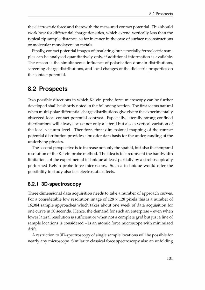
8.2 Prospects
the electrostatic force and therewith the measured contact potential. This shouldwork best for differential charge densities, which extend vertically less than thetypical tip sample distance, as for instance in the case of surface reconstructionsor molecular monolayers on metals.
Finally, contact potential images of insulating, but especially ferroelectric sam-ples can be analysed quantitatively only, if additional information is available.The reason is the simultaneous influence of polarisation domain distributions,screening charge distributions, and local changes of the dielectric properties onthe contact potential.
8.2 Prospects
Two possible directions in which Kelvin probe force microscopy can be furtherdeveloped shall be shortly noted in the following section. The first seems naturalwhen multi-polar differential charge distributions give rise to the experimentallyobserved local contact potential contrast. Especially, laterally strong confineddistributions will always cause not only a lateral but also a vertical variation ofthe local vacuum level. Therefore, three dimensional mapping of the contactpotential distribution provides a broader data basis for the understanding of theunderlying physics.
The second perspective is to increase not only the spatial, but also the temporalresolution of the Kelvin probe method. The idea is to circumvent the bandwidthlimitations of the experimental technique at least partially by a stroboscopicallyperformed Kelvin probe force microscopy. Such a technique would offer thepossibility to study also fast electrostatic effects.
8.2.1 3D-spectroscopy
Three dimensional data acquisition needs to take a number of approach curves.For a considerable low resolution image of 128× 128 pixels this is a number of16,384 sample approaches which takes about one week of data acquisition forone curve in 30 seconds. Hence, the demand for such an enterprise – even whenlower lateral resolution is sufficient or when not a complete grid but just a line ofsample locations is considered – is an atomic force microscope with minimizeddrift.
A restriction to 3D-spectroscopy of single sample locations will be possible fornearly any microscope. Similar to classical force spectroscopy also an unfolding
101
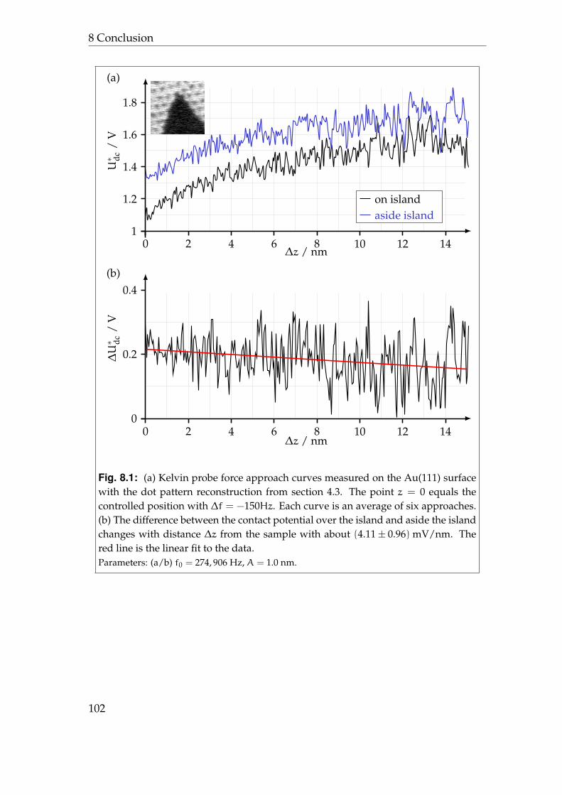
8 Conclusion
on islandaside island
(a)
∆z / nm
U∗ dc
/V
1
1.2
1.4
1.6
1.8
0 2 4 6 8 10 12 14
(b)
∆z / nm
∆U∗ dc
/V
0
0.2
0.4
0 2 4 6 8 10 12 14
Fig. 8.1: (a) Kelvin probe force approach curves measured on the Au(111) surfacewith the dot pattern reconstruction from section 4.3. The point z = 0 equals thecontrolled position with ∆f = −150Hz. Each curve is an average of six approaches.(b) The difference between the contact potential over the island and aside the islandchanges with distance ∆z from the sample with about (4.11± 0.96) mV/nm. Thered line is the linear fit to the data.Parameters: (a/b) f0 = 274, 906 Hz, A = 1.0 nm.
102
8.2 Prospects
of the error signal in frequency demodulation Kelvin probe force microscopyafter the method of Sader and Jarvis [179] for both sidebands should be possi-ble. While the sideband at ±ωm yields the product of the local contact potentialdifference and the capacitance gradient, the second sideband at ±2ωm dependsonly on the capacitance gradient. Therefore it can be used to separate out thecontribution of the local contact potential difference in the spectroscopic dataof the first sideband. Additionally, the same spectroscopy but with activatedKelvin feedback gives a second approach to the same physics and the opportu-nity to cross check the experiment.
In order to demonstrate the feasibility, approach curves have been taken onthe Au(111) surface with the dot pattern reconstruction from section 4.3. Figure8.1 shows the resulting contact potential versus distance curves as average of sixcurves on top of an island and of six approaches in between the dots. In bothcases the contact potential drops in the proximity of the surface. This indicates atip effect like for instance a charged cluster at the tip end.
Additionally, the contrast between the two areas increases closer to the sur-face, which is naturally the case for bipolar differential charge distributions onthe sample. Here, the slope of the increase measures (4.11± 0.96) mV/nm.
Careful analysis of such measurements should allow to come up with bettermodels for the differential charge density and a deeper understanding of theKelvin probe experiment.
8.2.2 Stroboscopic Kelvin probe force microscopy
In many fields of experimental physics time resolved measurements of physicalproperties are of great interest. In the case of Kelvin probe force microscopy thiscould be the time evolution of a charge density, transients of photo voltages orthe propagation of applied electrical signals.
Stroboscopic techniques are the key to high time resolution even for exper-imental setups which otherwise do not allow the measurement of fast signals[180]. The idea is to repeat the single experiment with a high repetition fre-quency and to measure a mean low-frequency signal which depends on a timedelay within the single experiment.
In order to further illustrate the concept, one example shall be discussed inmore detail. If for instance the transient of a photo voltage shall be measured,one would periodically illuminate (pump) the sample which causes a periodicphoto voltage Ulcpd(t), yet, maybe with certain time delays with respect to the
103
8 Conclusion
illumination. Then, triggered to the pump, voltage pulses are applied betweentip and sample which are delayed on purpose and amplitude modulated with asmall modulation frequency in order to enable a Kelvin feedback. Of interest isthe measured Kelvin voltage as function of the pulse delay time.
Letωr = 2π/Tr be the repetition frequency of the pump. Then the modulationbias is chopped with exactly the same frequencyωr such that the bias is appliedonly for a small time increment 2τ around the delay time td after the pump. Fora periodic pulse function Π(ωrt) these values translate into a phase incrementϕτ = ωr · τ and into a delay phase ϕd = ωr · td. With the pulse function
Π(t) =
{1, ϕd −ϕτ 6 ωrt− 2πk 6 ϕd +ϕτ k ∈ Z0, otherwise
(8.1)
the modulation bias can be written as Um(t) = um · sin(ωm · t) · Π(ωrt). Thesame calculation as in section 1.2 yields the electrostatic time dependent force
Fzel(~r, t) =12∂C(~r)
∂z·[{Udc +Ulcpd(~r, t)
}2+u2m
2·Π(ωrt)
]+
+∂C(~r)
∂z·{Udc +Ulcpd(~r, t)
}· um · sin(ωmt) ·Π(ωrt) +
+14∂C(~r)
∂z· u2m · sin(2ωmt) ·Π(ωrt), (8.2)
with the known consequences on the static shift of the equilibrium position, thedirect excitation of cantilever motion and the shift of the resonance frequency.
As long as ωr or one of its higher harmonics is not equal to any mechani-cal resonance frequency of the cantilever the demodulation lock-in measures asimple time average of any signal faster than the lock-in bandwidth (given byits time constant). Hence, a time dependent local contact potential differenceUlcpd(~r, t) = Ulcpd(~r) + Ulcpd(~r,ωrt) generates a Kelvin feedback signal propor-tional to:
X(td) ∝[Udc + Ulcpd(~r)
]· ϕτπ
+1Tr
∫ t0+Trt0
dt Ulcpd(~r,ωrt) ·Π(ωrt+ϕd), (8.3)
which now is a function of the delay time td. Therefore, the measured contactpotential is not only a function of the static part Ulcpd(~r) but allows also to extractthe averaged periodic time dependency of the voltage signal generated by thepump.
104
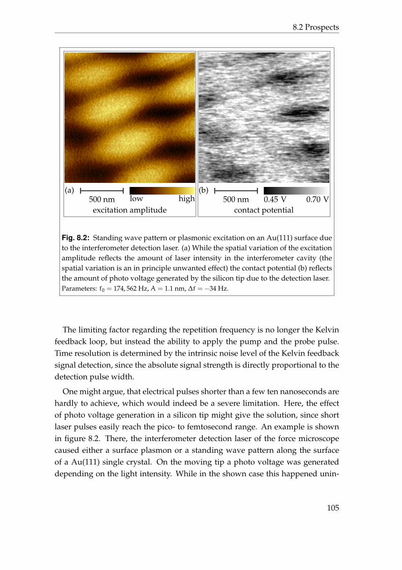
8.2 Prospects
(a)500 nm low highexcitation amplitude
(b)500 nm 0.45 V 0.70 V
contact potential
Fig. 8.2: Standing wave pattern or plasmonic excitation on an Au(111) surface dueto the interferometer detection laser. (a) While the spatial variation of the excitationamplitude reflects the amount of laser intensity in the interferometer cavity (thespatial variation is an in principle unwanted effect) the contact potential (b) reflectsthe amount of photo voltage generated by the silicon tip due to the detection laser.Parameters: f0 = 174, 562 Hz, A = 1.1 nm, ∆f = −34 Hz.
The limiting factor regarding the repetition frequency is no longer the Kelvinfeedback loop, but instead the ability to apply the pump and the probe pulse.Time resolution is determined by the intrinsic noise level of the Kelvin feedbacksignal detection, since the absolute signal strength is directly proportional to thedetection pulse width.
One might argue, that electrical pulses shorter than a few ten nanoseconds arehardly to achieve, which would indeed be a severe limitation. Here, the effectof photo voltage generation in a silicon tip might give the solution, since shortlaser pulses easily reach the pico- to femtosecond range. An example is shownin figure 8.2. There, the interferometer detection laser of the force microscopecaused either a surface plasmon or a standing wave pattern along the surfaceof a Au(111) single crystal. On the moving tip a photo voltage was generateddepending on the light intensity. While in the shown case this happened unin-
105
8 Conclusion
tentionally, one could facilitate the same effect for stroboscopic experiments withhigh time resolution.
8.3 Closing remarks
Lord Kelvins first experiments lie more than a century back in the past. The mi-croscopic realisation of the experiment initiated a renaissance with very fruitfulapplications in many fields of scientific research. The same might happen, whenactual limitations are eluded and a new kind of physical information becomesaccessible. Abilities to measure electric potentials with high resolution in spaceand time possibly combined with similar investigations of magnetic fields couldeven allow for nanoscopic electrodynamic experiments. Future will show wherethe evolution of Kelvin probe force microscopy goes, but surely it will bring upmany interesting scientific challenges in the field of nanotechnology.
106

Part III
Appendix

A Piezoresponse force microscopy
Technical skill is mastery of complexity, while creativ-ity is mastery of simplicity.
Christopher Zeeman
Piezoresponse force microscopy is a scanning probe microscopy methodwhich aims to resolve local changes in the piezoelectric properties of the sample[181]. Especially in ferroelectric materials the method enables to resolve the localdomain structure. The working principle is as follows: between the tip, whichhas to be in contact with the sample surface, and a back contact at the sample asinusoidal excitation voltage is applied. Due to the converse piezoelectric effectthe sample starts to oscillate at the excitation frequency which leads also to amovement of the tip. Using lock-in technique to analyse the deflection signal,both magnitude and direction of the sample oscillation can be recorded. If aforce microscope with beam deflection is used, the vertical and lateral deflectionsignals can be analysed separately, which enables to measure two of three com-ponents of the polarisation vector simultaneously. If the sample is rotated andthe third component is also measured, a complete reconstruction of the domaindistribution is possible, given that the crystal orientation and the piezoelectrictensor1
dij =
(∂Sj
∂Ei
)T(A.1)
is known. The notation is: E electric field, T mechanical stress, and Smechanicalstrain. A schematic representation of the technique is shown in figure A.1.
If an additional bias is applied between tip and sample, the piezoelectric re-sponse can be measured as function of the external electric field, which allowsto locally record the polarisation hysteresis of ferroelectric materials. From suchhysteresis curves the coercive voltages can be extracted which are important forswitching experiments and local domain engineering.
1Here in Voigt notation.
109
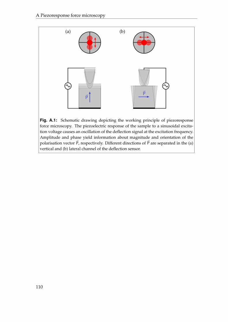
A Piezoresponse force microscopy
(a)
~P
(b)
~P
Fig. A.1: Schematic drawing depicting the working principle of piezoresponseforce microscopy. The piezoelectric response of the sample to a sinusoidal excita-tion voltage causes an oscillation of the deflection signal at the excitation frequency.Amplitude and phase yield information about magnitude and orientation of thepolarisation vector ~P, respectively. Different directions of ~P are separated in the (a)vertical and (b) lateral channel of the deflection sensor.
110
B Kelvin application note
Explanation separates us from astonishment, which isthe only gateway to the incomprehensible.
Eugene Ionesco
The following section shall give a brief introduction on how to run Kelvinprobe force microscopy on the RHK SPM100 with PLLPro2.
Both detection schemes – amplitude demodulation and frequency demodu-lation – are possible and can be chosen after personal favour. Since in the PLL-Pro2 both available lock-in amplifiers and the phase-locked loop run on the samefield-programmable gate area, a direct sideband detection in frequency demod-ulation mode is possible. Whether to perform indirect sideband detection usingtwo lock-in amplifiers or direct sideband detection using a single lock-in am-plifier depends mostly on the cantilever oscillation signal amplitude. In Kelvinprobe force microscopy the magnitude of the sideband signal is typically aboutone to ten percent of the carrier. Since the detection noise of a lock-in amplifieris closely connected to the chosen bandwidth and therewith to the scan velocity,a minimal carrier signal magnitude of about 1 V is necessary in order to achievea reasonable signal-to-noise ratio for a typical bandwidth of 128 Hz. In whatfollows a practical recipe for each of the operation modes is given. For a generaldescription of the method please refer to section 1.2.
Amplitude demodulation
In order to perform amplitude demodulation Kelvin probe force microscopy un-der resonant conditions the following steps should be done before the sample isapproached:
• search for the eigenfrequencies of the cantilever
• set up the phase locked loop and switch it on
• set the modulation bias parameters:
111
B Kelvin application note
– determine the ratio between the modulation frequency and the oscil-lation frequency (e.g. the ratio between the first and the fundamentaleigenfrequency) and set the resulting value into lock to pll in the Kelvinand z menu of the PllPro2
– set the modulation frequency offset to zero
– set the modulation amplitude as high as possible in the experiment.In most cases modulation amplitudes below 500 mV won’t give sig-nificant change to the measured U∗dc.
• set up the lock-in amplifier. In the Additional lock-ins menu of the PllPro2two lock-in amplifiers are available. By default the X-channel of lock-inamplifier number one (lia1) is used as error signal for the Kelvin controller,as not only the amplitude but also the phase of the cantilever response areimportant. The setup of lia1 should be done at least once when approach-ing the sample first time:
– chose feedback input as input signal for lia1
– set the same value into lock to pll of lia1 as for the Kelvin excitation
– set frequency offset from pll to zero
– set a slow filter for lia1 (10 Hz 18 dB). This enables later to set thecorrect phase offset.
• set up the Kelvin controller for approach:
– set the Kelvin controller mode to force
– set the applied bias to +5 V. This ensures a “soft” landing of the tipapproach due to the high attractive electrostatic force.
Then approach the surface. When the approach is finished and the topographycontroller is in feedback, a change of the applied bias should lead to a change ofthe z-position. The minimal z corresponds to Udc = U∗dc,static. If this specialU∗dc is found, increase the bias again by about 1 V and compensate the shift inz-position by changing the topography set point. This increases the tip samplecapacitance and thus also the magnitude of the Kelvin error signal. Now, thephase-channel of lia1 shows an arbitrary but fix value, which shall be set to zerowith the automatic zero button of lia11.1Note: As there is still a bug in the PllPro2 a change crossing ±180°will be ignored. Theworkaround is to set the correct phase by hand.
112
Before activating the Kelvin controller the PI-values of the controller and thefilter of the lia1 should be set according to imaging speed. The topography setpoint should be set back to a gentle feedback as a large portion of the interactionforce will be compensated with activated Kelvin controller. Finally, the Kelvincontroller can be set to unlimited or limited with appropriate limits2. In the Addi-tional lock-ins menu the Kelvin channel displays the actual value of Udc and canbe connected to one of the DAC’s of the PllPro2.
Direct sideband detection
When frequency demodulation Kelvin probe force microscopy shall be per-formed, high carrier signal strength allows for direct sideband detection. Inpractice following steps should be done before approaching the surface:
• set up the phase-locked loop and switch it on
• set the modulation bias parameters:
– use the Kelvin and z menu of the PllPro2 to set the modulation fre-quency.
– set the modulation amplitude as high as possible in the experiment.In most cases modulation amplitudes below 500 mV won’t give sig-nificant change to the measured U∗dc.
• set up the lock-in amplifier. In the Additional lock-ins menu of the PllPro2two lock-in amplifiers are available. By default the X-channel of lock-innumber one (lia1) is used as error-signal for the KPFM controller, as notonly the amplitude but also the phase of the cantilever response are impor-tant. The setup of lia1 should be done at least once when approaching thesample first time:
– chose feedback input as input signal for lia1
– set frequency offset from pll to the modulation frequency
– set lock to pll of lia1 to 1
– set a slow filter for lia1 (10 Hz 18 dB). This enables later to set thecorrect phase offset.
• set up the controller for approach:
2This is U∗dc has to be in between the limits.
113
B Kelvin application note
– set the Kelvin controller to force
– set the applied bias to +5 V. This ensures a “soft” landing of the tipapproach due to the high attractive electrostatic force.
The further procedure beginning from the start of the tip sample approach isequal to the case of amplitude demodulation described above.
Indirect sideband detection
When frequency demodulation Kelvin probe force microscopy shall be per-formed, a low carrier signal magnitude demands for indirect sideband detection.The advantage of this technique is better control over the signal-to-noise ratio ofthe Kelvin error signal. Unfortunately, it has need for two lock-in amplifiers,one DAC and the second fast signal input. In practice following steps should bedone before approaching the surface:
• set up the phase-locked loop and switch it on
• set the modulation bias parameters:
– use the Kelvin and z menu of the PllPro2 to set the modulation fre-quency.
– set the modulation amplitude as high as possible in the experiment.In most cases modulation amplitudes below 500 mV won’t give sig-nificant change to the measured U∗dc.
• set up the lock-in amplifiers. In the Additional lock-ins menu of the PllPro2two lock-in amplifiers are available. By default the X-channel of lock-inamplifier number one (lia1) is used as error-signal for the Kelvin controller,as not only the amplitude but also the phase of the cantilever response areimportant. Lock-in amplifier number two (lia2) is used for demodulationof the feedback signal:
– chose feedback input as input signal for lia2
– set frequency offset from pll of lia2 to zero
– set lock to pll of lia2 to 1
– set a slow filter for lia2 (10 Hz 18 dB). This enables to set the correctphase offset.
114
– use the automatic zero button of lia2 to set the correct phase3.
– set a fast filter for lia2, the bandwidth should at least allow the Kelvinmodulation frequency to pass
– physically connect DAC-4 to the second fast signal input of the PllPro2
– chose DAC-4 as output for the X-channel of lia2 with appropriate am-plification. The signal at DAC-4 shall not exceed 1 V4.
– chose second fast signal input as input signal for lia1
– set frequency offset from pll of lia1 to the modulation frequency
– set lock to pll of lia1 to zero
– set a slow filter for lia1 (10 Hz 18 dB). This enables later to set thecorrect phase offset.
• set up the controller for approach:
– set the KPFM controller to force
– set the applied bias to +5 V. This ensures a “soft” landing of the tipapproach due to the high electrostatic force.
The further procedure beginning from the start of the tip sample approach isequal to the case of amplitude demodulation described above.
3Note: As there is still a bug in the PllPro2 a change crossing ±180°will be ignored.4Otherwise the second fast signal input will be in overload.
115

C Calculation of local workfunctions with circular shapedmodel charge densities
Computers can figure out all kinds of problems, exceptthe things in the world that just don’t add up.
James Magary
Here, a general solution for the potential distribution around a circular shapedcharge density with radius R and thickness 2d shall be derived. The charge dis-tribution ρ(~r) is modelled uniform within the circular bounds but may have anarbitrary distribution in z-direction, given by the distribution function f(z):
ρ(~r) =
{σ · f(z) , x2 + y2 6 R
0 , x2 + y2 > R(C.1)
For simplicity, the distribution function f(z) shall fulfil the conditions:
∀ z < −d and d < z : f(z) = 0 (C.2)∫d−d
dz f(z) = 0 (C.3)∫d0
dz f(z) = 1. (C.4)
After Coulomb’s law the electric field is given by
~E(~r) =1
4πε0
∫V
d3r′ ρ(~r′) · ~r−~r′
|~r−~r′|3. (C.5)
Due to the symmetry of the problem cylindrical coordinates are suited best forthe integration. Furthermore the z-component of the electric field in the planey = 0 is sufficient for the computation of the electrostatic potential, since forz→∞ the potential has to vanish. Then the integral reduces with~r′ = (~κ, z′) to
117
C Calculation with model charge densities
Ez(x, 0, z) =σ
4πε0
∫d−d
dz′∫π−π
dϕ∫R
0dκ f(z′) · κ · (z− z
′)
|~r−~r′|3. (C.6)
Besides scaling out the dipole length d, the integral can be described best,if the origin of the integration coordinate system is shifted to the point (x,0,0).Then the integration splits up into two solutions – one for x 6 R and one forx > R – given by:
x 6 R:
Ez = −σ
2ε0
∫1
−1dz′f(d · z′)
∫1
0dϕ
z− z′√κ1(ϕ)2 + (z− z′)2
(C.7)
κ1(ϕ) = −x cos(πϕ) +√R2 − x2 sin2(πϕ) (C.8)
x > R:
Ez = −σ
2ε0
∫1
−1dz′f(d · z′)
∫ ϕ0
0dϕ
[z− z′√
κ2(ϕ)2 + (z− z′)2− (C.9)
−z− z′√
κ1(ϕ)2 + (z− z′)2
](C.10)
κ2,1(ϕ) = x cos(πϕ)±√R2 − x2 sin2(πϕ) (C.11)
ϕ0 =1π
arcsin(R
x
)(C.12)
The electrostatic potential is derived by integration as
φ(x, 0, z) =∫∞z
dz′ Ez(x, 0, z′). (C.13)
118

D Picture gallery
I never read, I just looked at pictures.
Andy Warhol
119
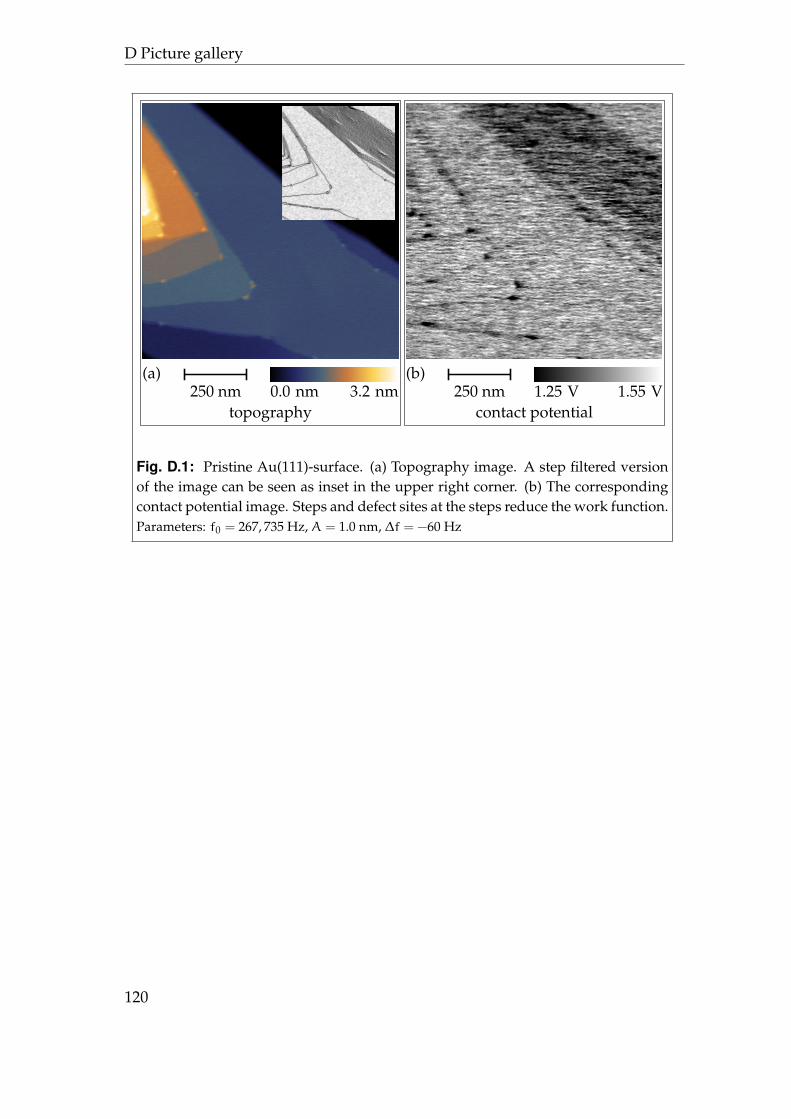
D Picture gallery
(a)250 nm 0.0 nm 3.2 nm
topography
(b)250 nm 1.25 V 1.55 V
contact potential
Fig. D.1: Pristine Au(111)-surface. (a) Topography image. A step filtered versionof the image can be seen as inset in the upper right corner. (b) The correspondingcontact potential image. Steps and defect sites at the steps reduce the work function.Parameters: f0 = 267, 735 Hz, A = 1.0 nm, ∆f = −60 Hz
120
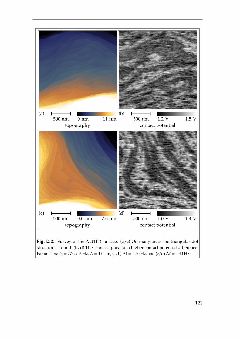
(a)500 nm 0 nm 11 nm
topography
(b)500 nm 1.2 V 1.5 V
contact potential
(c)500 nm 0.0 nm 7.6 nm
topography
(d)500 nm 1.0 V 1.4 V
contact potential
Fig. D.2: Survey of the Au(111) surface. (a/c) On many areas the triangular dotstructure is found. (b/d) These areas appear at a higher contact potential difference.Parameters: f0 = 274, 906 Hz, A = 1.0 nm, (a/b) ∆f = −50 Hz, and (c/d) ∆f = −40 Hz.
121
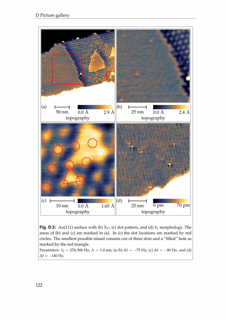
D Picture gallery
(a)50 nm 0.0 A 2.9 A
topography
(b)25 nm 0.0 A 2.4 A
topography
(c)10 nm 0.0 A 1.65 A
topography
(d)25 nm 0 pm 70 pm
topography
Fig. D.3: Au(111) surface with (b) S2-, (c) dot pattern, and (d) S1 morphology. Theareas of (b) and (c) are marked in (a). In (c) the dot locations are marked by redcircles. The smallest possible island consists out of three dots and a “filled” hole asmarked by the red triangle.Parameters: f0 = 274, 906 Hz, A = 1.0 nm, (a/b) ∆f = −75 Hz, (c) ∆f = −80 Hz, and (d)∆f = −140 Hz.
122
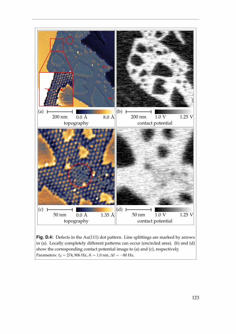
(a)200 nm 0.0 A 8.0 A
topography
(b)200 nm 1.0 V 1.25 V
contact potential
(c)50 nm 0.0 A 1.35 A
topography
(d)50 nm 1.0 V 1.25 V
contact potential
Fig. D.4: Defects in the Au(111) dot pattern. Line splittings are marked by arrowsin (a). Locally completely different patterns can occur (encircled area). (b) and (d)show the corresponding contact potential image to (a) and (c), respectively.Parameters: f0 = 274, 906 Hz, A = 1.0 nm, ∆f = −80 Hz.
123
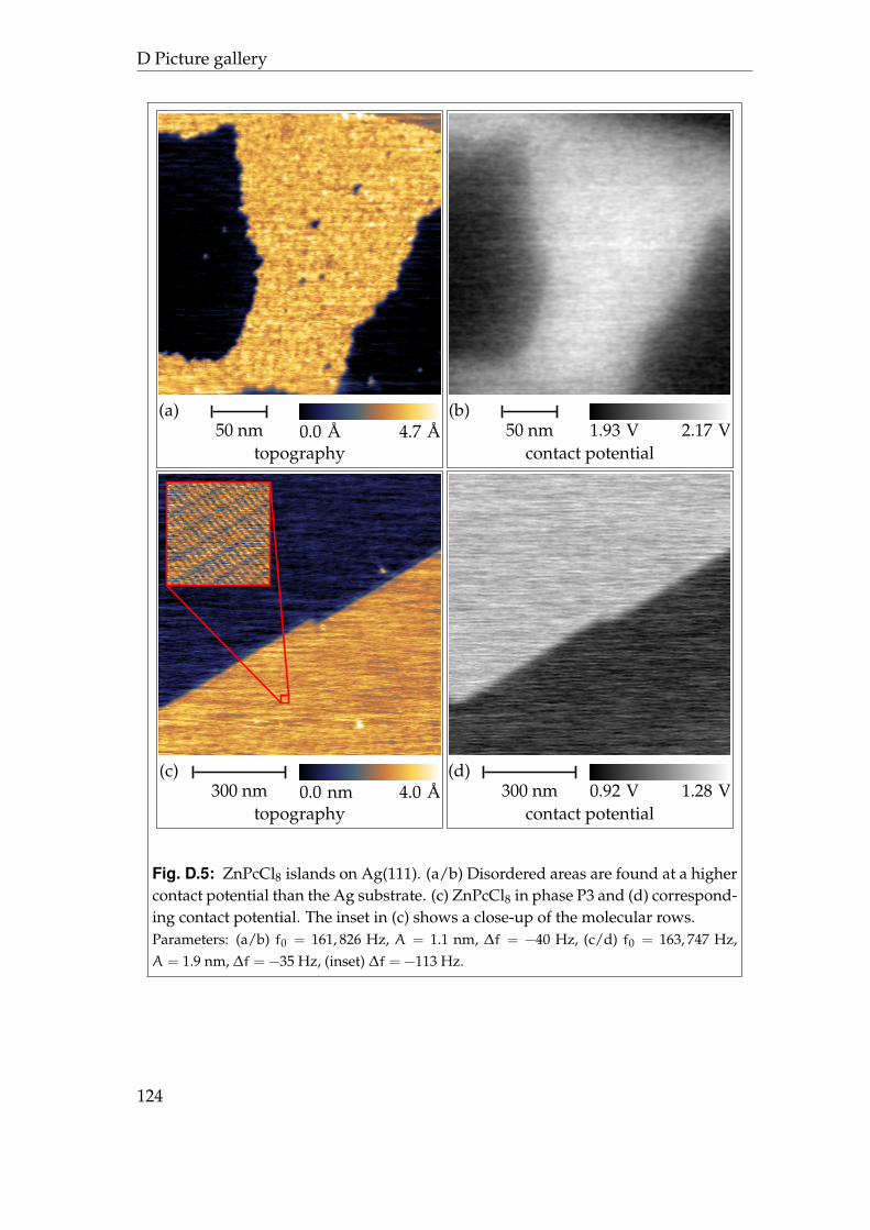
D Picture gallery
(a)50 nm 0.0 A 4.7 A
topography
(b)50 nm 1.93 V 2.17 V
contact potential
(c)300 nm 0.0 nm 4.0 A
topography
(d)300 nm 0.92 V 1.28 V
contact potential
Fig. D.5: ZnPcCl8 islands on Ag(111). (a/b) Disordered areas are found at a highercontact potential than the Ag substrate. (c) ZnPcCl8 in phase P3 and (d) correspond-ing contact potential. The inset in (c) shows a close-up of the molecular rows.Parameters: (a/b) f0 = 161, 826 Hz, A = 1.1 nm, ∆f = −40 Hz, (c/d) f0 = 163, 747 Hz,A = 1.9 nm, ∆f = −35 Hz, (inset) ∆f = −113 Hz.
124
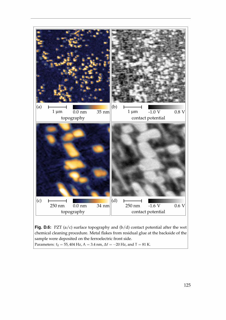
(a)1 µm 0.0 nm 35 nm
topography
(b)1 µm -1.0 V 0.8 V
contact potential
(c)250 nm 0.0 nm 34 nm
topography
(d)250 nm -1.6 V 0.6 V
contact potential
Fig. D.6: PZT (a/c) surface topography and (b/d) contact potential after the wetchemical cleaning procedure. Metal flakes from residual glue at the backside of thesample were deposited on the ferroelectric front side.Parameters: f0 = 55, 404 Hz, A = 3.4 nm, ∆f = −20 Hz, and T = 81 K.
125
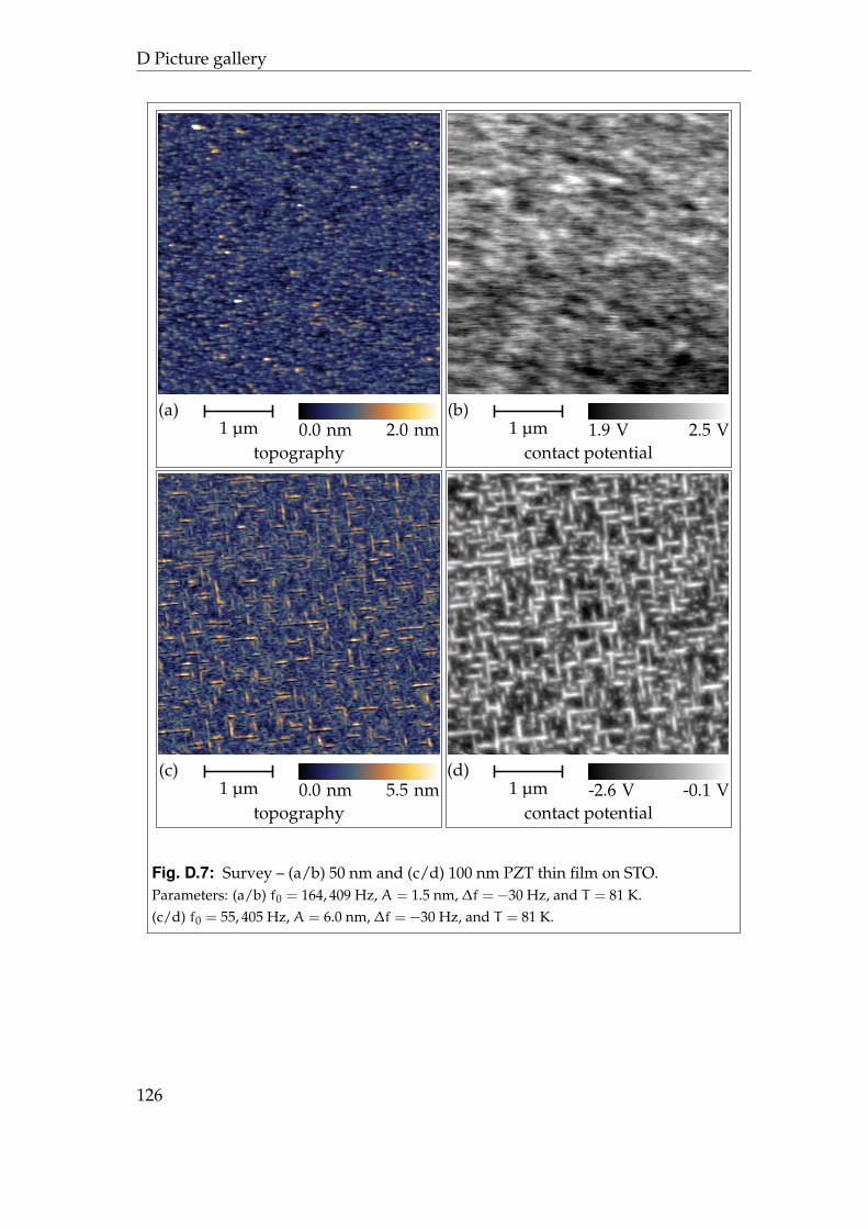
D Picture gallery
(a)1 µm 0.0 nm 2.0 nm
topography
(b)1 µm 1.9 V 2.5 V
contact potential
(c)1 µm 0.0 nm 5.5 nm
topography
(d)1 µm -2.6 V -0.1 V
contact potential
Fig. D.7: Survey – (a/b) 50 nm and (c/d) 100 nm PZT thin film on STO.Parameters: (a/b) f0 = 164, 409 Hz, A = 1.5 nm, ∆f = −30 Hz, and T = 81 K.(c/d) f0 = 55, 405 Hz, A = 6.0 nm, ∆f = −30 Hz, and T = 81 K.
126
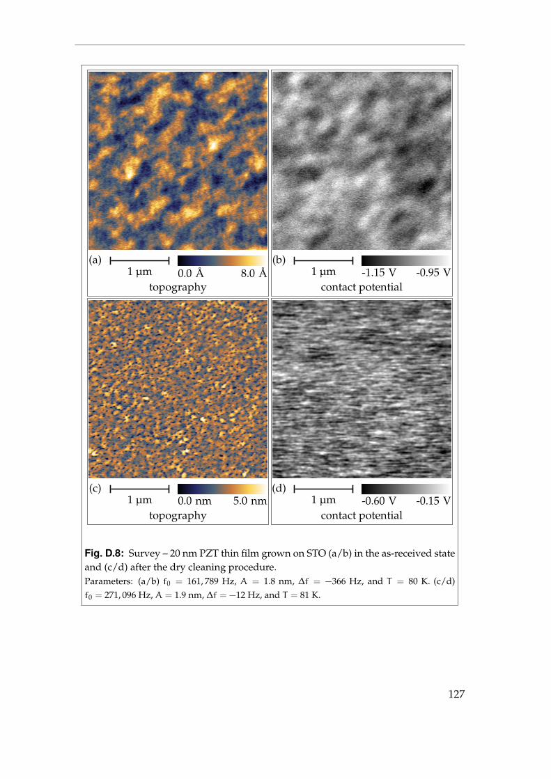
(a)1 µm 0.0 A 8.0 A
topography
(b)1 µm -1.15 V -0.95 V
contact potential
(c)1 µm 0.0 nm 5.0 nm
topography
(d)1 µm -0.60 V -0.15 V
contact potential
Fig. D.8: Survey – 20 nm PZT thin film grown on STO (a/b) in the as-received stateand (c/d) after the dry cleaning procedure.Parameters: (a/b) f0 = 161, 789 Hz, A = 1.8 nm, ∆f = −366 Hz, and T = 80 K. (c/d)f0 = 271, 096 Hz, A = 1.9 nm, ∆f = −12 Hz, and T = 81 K.
127
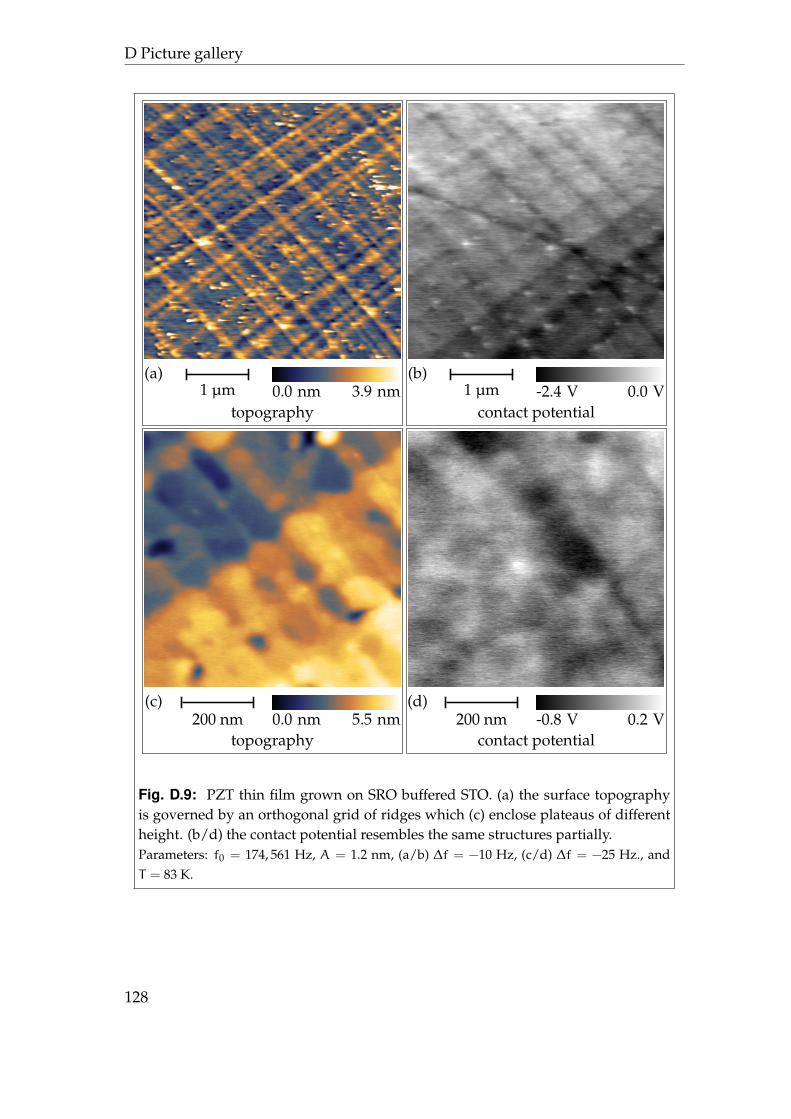
D Picture gallery
(a)1 µm 0.0 nm 3.9 nm
topography
(b)1 µm -2.4 V 0.0 V
contact potential
(c)200 nm 0.0 nm 5.5 nm
topography
(d)200 nm -0.8 V 0.2 V
contact potential
Fig. D.9: PZT thin film grown on SRO buffered STO. (a) the surface topographyis governed by an orthogonal grid of ridges which (c) enclose plateaus of differentheight. (b/d) the contact potential resembles the same structures partially.Parameters: f0 = 174, 561 Hz, A = 1.2 nm, (a/b) ∆f = −10 Hz, (c/d) ∆f = −25 Hz., andT = 83 K.
128
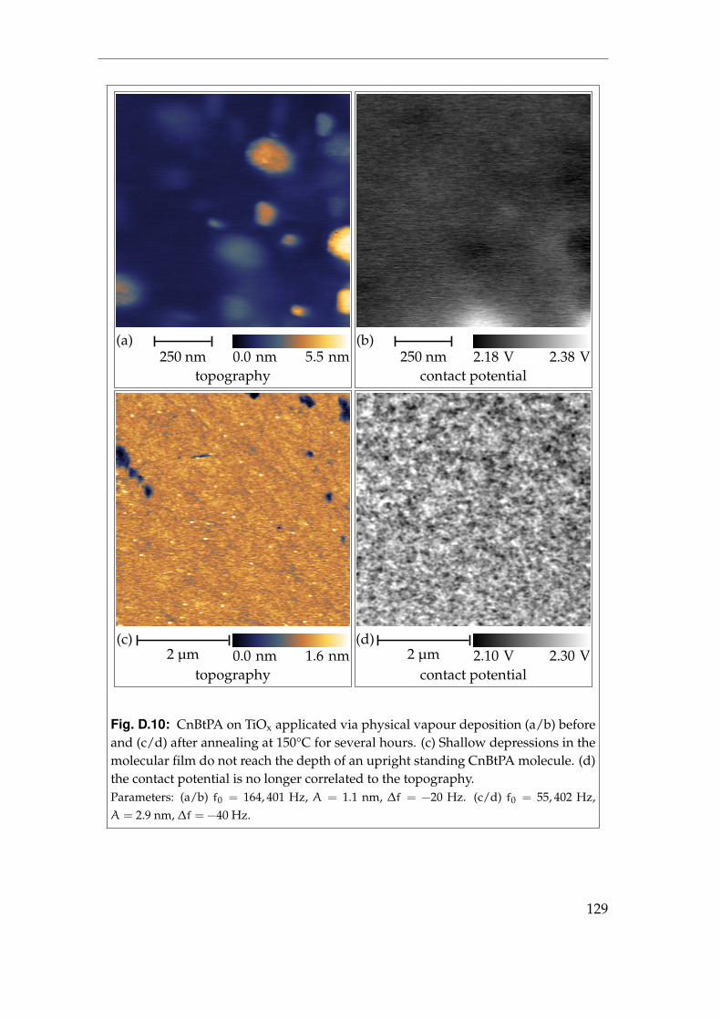
(a)250 nm 0.0 nm 5.5 nm
topography
(b)250 nm 2.18 V 2.38 V
contact potential
(c)2 µm 0.0 nm 1.6 nm
topography
(d)2 µm 2.10 V 2.30 V
contact potential
Fig. D.10: CnBtPA on TiOx applicated via physical vapour deposition (a/b) beforeand (c/d) after annealing at 150°C for several hours. (c) Shallow depressions in themolecular film do not reach the depth of an upright standing CnBtPA molecule. (d)the contact potential is no longer correlated to the topography.Parameters: (a/b) f0 = 164, 401 Hz, A = 1.1 nm, ∆f = −20 Hz. (c/d) f0 = 55, 402 Hz,A = 2.9 nm, ∆f = −40 Hz.
129
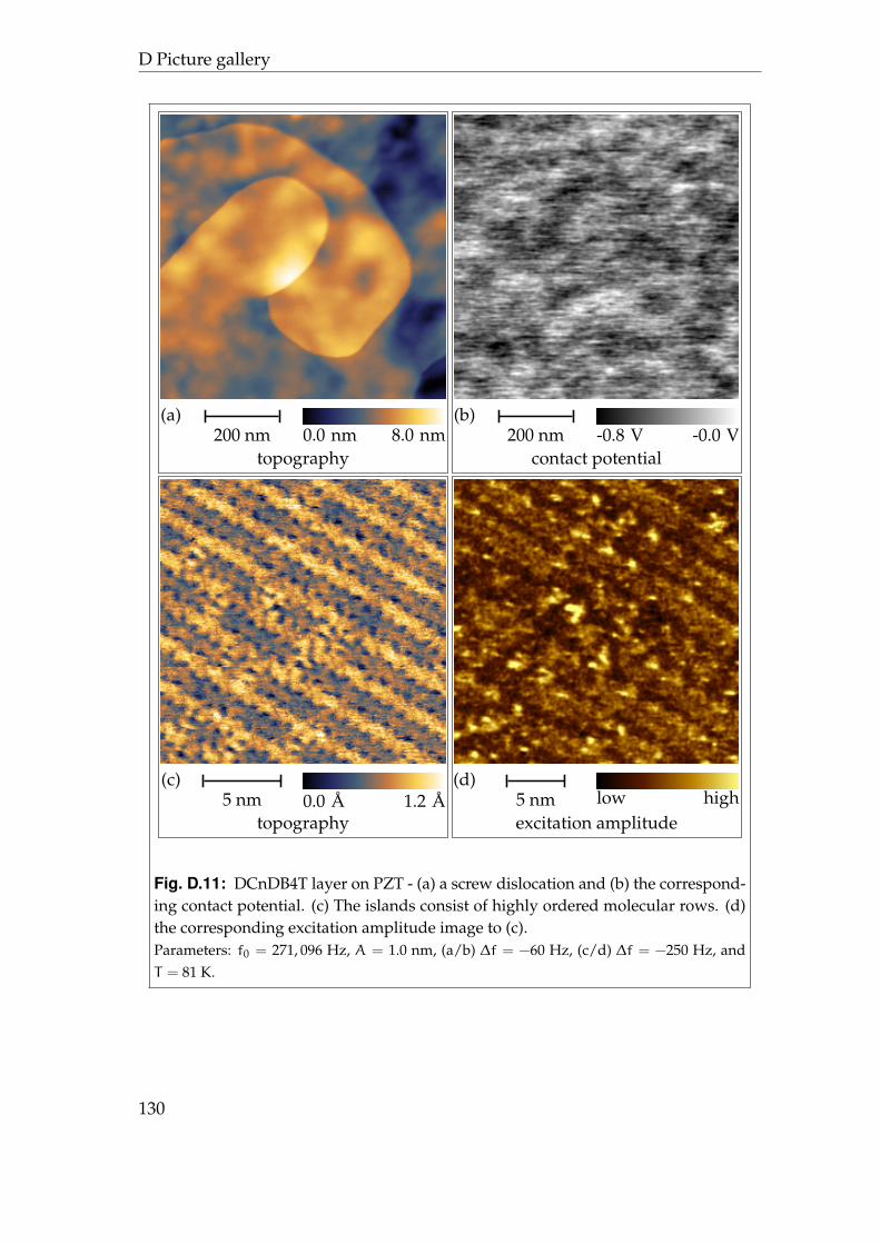
D Picture gallery
(a)200 nm 0.0 nm 8.0 nm
topography
(b)200 nm -0.8 V -0.0 V
contact potential
(c)5 nm 0.0 A 1.2 A
topography
(d)5 nm low highexcitation amplitude
Fig. D.11: DCnDB4T layer on PZT - (a) a screw dislocation and (b) the correspond-ing contact potential. (c) The islands consist of highly ordered molecular rows. (d)the corresponding excitation amplitude image to (c).Parameters: f0 = 271, 096 Hz, A = 1.0 nm, (a/b) ∆f = −60 Hz, (c/d) ∆f = −250 Hz, andT = 81 K.
130
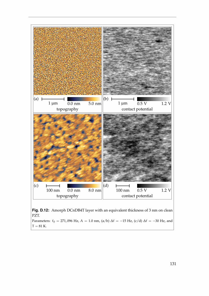
(a)1 µm 0.0 nm 5.0 nm
topography
(b)1 µm 0.5 V 1.2 V
contact potential
(c)100 nm 0.0 nm 8.0 nm
topography
(d)100 nm 0.5 V 1.2 V
contact potential
Fig. D.12: Amorph DCnDB4T layer with an equivalent thickness of 3 nm on cleanPZT.Parameters: f0 = 271, 096 Hz, A = 1.0 nm, (a/b) ∆f = −15 Hz, (c/d) ∆f = −30 Hz, andT = 81 K.
131

Bibliography
[1] A. Volta. On the Electricity excited by the mere Contact of conductingSubstances of different kinds. Phil. Trans. R. Soc. Lond., 90:403, 1800.
[2] F. Steinle. Explorative Experimente. Franz Steiner Verlag, 2005.
[3] A. Volta. On the Electricity excited by the mere Contact of conductingSubstances of different kinds. Philosophical Magazine Series 1, 7:298, 1800.
[4] J.W. Ritter. Versuche und Bemerkungen uber den Galvanismus der Voltais-chen Batterie. Annalen der Physik, 7:431, 1801.
[5] Lord Kelvin. Contact Electricity of Metals. Phil. Mag., 46:82, 1898.
[6] G. Binnig, C.F. Quate, and Ch. Gerber. Atomic Force Microscopy. Phys.Rev. Lett., 56:930, 1986.
[7] G. Binnig and H. Rohrer. Scanning tunneling microscopy. Helv. Phys. Acta,55:726, 1982.
[8] T.R. Albrecht, P. Grutter, D. Horne, and D. Rugar. Frequency modulationdetection using high-Q cantilevers for enhanced force microscope sensi-tivity. J. Appl. Phys., 69:668, 1986.
[9] Y. Martin, C.C. Williams, and H.K. Wickramasinghe. Atomic forcemicroscope-force mapping and profiling on a sub 100-a scale. J. Appl. Phys.,61:4723, 1987.
[10] U. Durig, R.H. Steinauer, and N. Blanc. Dynamic force microscopy bymeans of the phase-controlled oscillator method. J. Appl. Phys., 82:3641,1997.
[11] Ch. Loppacher. Entwicklung einer Digitalelektronik fur die Nichtkontakt-Rasterkraftmikroskopie basierend auf PLL-Technik. Diplomarbeit,Philosophisch-Naturwissenschaftliche Fakultat, Universitat Basel, 1995.
I
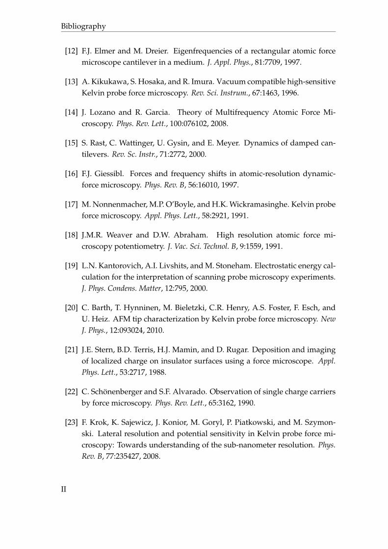
Bibliography
[12] F.J. Elmer and M. Dreier. Eigenfrequencies of a rectangular atomic forcemicroscope cantilever in a medium. J. Appl. Phys., 81:7709, 1997.
[13] A. Kikukawa, S. Hosaka, and R. Imura. Vacuum compatible high-sensitiveKelvin probe force microscopy. Rev. Sci. Instrum., 67:1463, 1996.
[14] J. Lozano and R. Garcia. Theory of Multifrequency Atomic Force Mi-croscopy. Phys. Rev. Lett., 100:076102, 2008.
[15] S. Rast, C. Wattinger, U. Gysin, and E. Meyer. Dynamics of damped can-tilevers. Rev. Sc. Instr., 71:2772, 2000.
[16] F.J. Giessibl. Forces and frequency shifts in atomic-resolution dynamic-force microscopy. Phys. Rev. B, 56:16010, 1997.
[17] M. Nonnenmacher, M.P. O’Boyle, and H.K. Wickramasinghe. Kelvin probeforce microscopy. Appl. Phys. Lett., 58:2921, 1991.
[18] J.M.R. Weaver and D.W. Abraham. High resolution atomic force mi-croscopy potentiometry. J. Vac. Sci. Technol. B, 9:1559, 1991.
[19] L.N. Kantorovich, A.I. Livshits, and M. Stoneham. Electrostatic energy cal-culation for the interpretation of scanning probe microscopy experiments.J. Phys. Condens. Matter, 12:795, 2000.
[20] C. Barth, T. Hynninen, M. Bieletzki, C.R. Henry, A.S. Foster, F. Esch, andU. Heiz. AFM tip characterization by Kelvin probe force microscopy. NewJ. Phys., 12:093024, 2010.
[21] J.E. Stern, B.D. Terris, H.J. Mamin, and D. Rugar. Deposition and imagingof localized charge on insulator surfaces using a force microscope. Appl.Phys. Lett., 53:2717, 1988.
[22] C. Schonenberger and S.F. Alvarado. Observation of single charge carriersby force microscopy. Phys. Rev. Lett., 65:3162, 1990.
[23] F. Krok, K. Sajewicz, J. Konior, M. Goryl, P. Piatkowski, and M. Szymon-ski. Lateral resolution and potential sensitivity in Kelvin probe force mi-croscopy: Towards understanding of the sub-nanometer resolution. Phys.Rev. B, 77:235427, 2008.
II
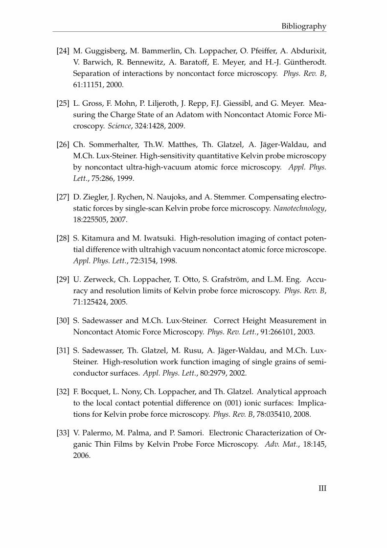
Bibliography
[24] M. Guggisberg, M. Bammerlin, Ch. Loppacher, O. Pfeiffer, A. Abdurixit,V. Barwich, R. Bennewitz, A. Baratoff, E. Meyer, and H.-J. Guntherodt.Separation of interactions by noncontact force microscopy. Phys. Rev. B,61:11151, 2000.
[25] L. Gross, F. Mohn, P. Liljeroth, J. Repp, F.J. Giessibl, and G. Meyer. Mea-suring the Charge State of an Adatom with Noncontact Atomic Force Mi-croscopy. Science, 324:1428, 2009.
[26] Ch. Sommerhalter, Th.W. Matthes, Th. Glatzel, A. Jager-Waldau, andM.Ch. Lux-Steiner. High-sensitivity quantitative Kelvin probe microscopyby noncontact ultra-high-vacuum atomic force microscopy. Appl. Phys.Lett., 75:286, 1999.
[27] D. Ziegler, J. Rychen, N. Naujoks, and A. Stemmer. Compensating electro-static forces by single-scan Kelvin probe force microscopy. Nanotechnology,18:225505, 2007.
[28] S. Kitamura and M. Iwatsuki. High-resolution imaging of contact poten-tial difference with ultrahigh vacuum noncontact atomic force microscope.Appl. Phys. Lett., 72:3154, 1998.
[29] U. Zerweck, Ch. Loppacher, T. Otto, S. Grafstrom, and L.M. Eng. Accu-racy and resolution limits of Kelvin probe force microscopy. Phys. Rev. B,71:125424, 2005.
[30] S. Sadewasser and M.Ch. Lux-Steiner. Correct Height Measurement inNoncontact Atomic Force Microscopy. Phys. Rev. Lett., 91:266101, 2003.
[31] S. Sadewasser, Th. Glatzel, M. Rusu, A. Jager-Waldau, and M.Ch. Lux-Steiner. High-resolution work function imaging of single grains of semi-conductor surfaces. Appl. Phys. Lett., 80:2979, 2002.
[32] F. Bocquet, L. Nony, Ch. Loppacher, and Th. Glatzel. Analytical approachto the local contact potential difference on (001) ionic surfaces: Implica-tions for Kelvin probe force microscopy. Phys. Rev. B, 78:035410, 2008.
[33] V. Palermo, M. Palma, and P. Samori. Electronic Characterization of Or-ganic Thin Films by Kelvin Probe Force Microscopy. Adv. Mat., 18:145,2006.
III
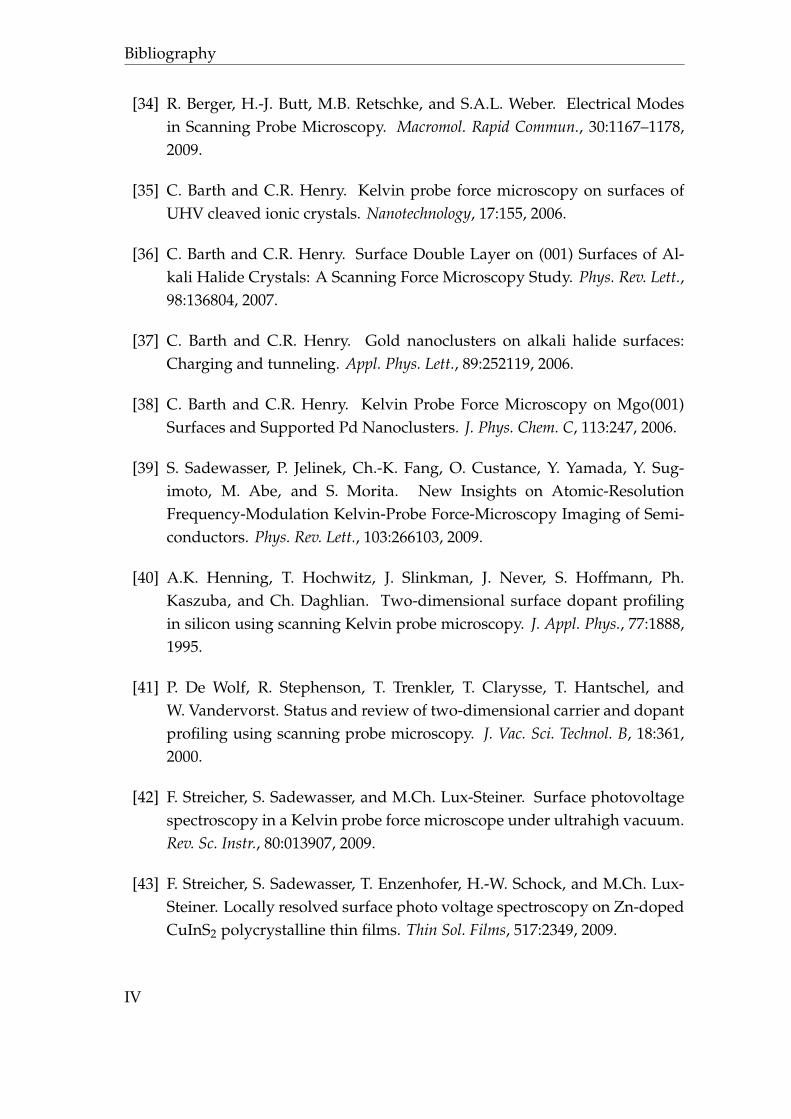
Bibliography
[34] R. Berger, H.-J. Butt, M.B. Retschke, and S.A.L. Weber. Electrical Modesin Scanning Probe Microscopy. Macromol. Rapid Commun., 30:1167–1178,2009.
[35] C. Barth and C.R. Henry. Kelvin probe force microscopy on surfaces ofUHV cleaved ionic crystals. Nanotechnology, 17:155, 2006.
[36] C. Barth and C.R. Henry. Surface Double Layer on (001) Surfaces of Al-kali Halide Crystals: A Scanning Force Microscopy Study. Phys. Rev. Lett.,98:136804, 2007.
[37] C. Barth and C.R. Henry. Gold nanoclusters on alkali halide surfaces:Charging and tunneling. Appl. Phys. Lett., 89:252119, 2006.
[38] C. Barth and C.R. Henry. Kelvin Probe Force Microscopy on Mgo(001)Surfaces and Supported Pd Nanoclusters. J. Phys. Chem. C, 113:247, 2006.
[39] S. Sadewasser, P. Jelinek, Ch.-K. Fang, O. Custance, Y. Yamada, Y. Sug-imoto, M. Abe, and S. Morita. New Insights on Atomic-ResolutionFrequency-Modulation Kelvin-Probe Force-Microscopy Imaging of Semi-conductors. Phys. Rev. Lett., 103:266103, 2009.
[40] A.K. Henning, T. Hochwitz, J. Slinkman, J. Never, S. Hoffmann, Ph.Kaszuba, and Ch. Daghlian. Two-dimensional surface dopant profilingin silicon using scanning Kelvin probe microscopy. J. Appl. Phys., 77:1888,1995.
[41] P. De Wolf, R. Stephenson, T. Trenkler, T. Clarysse, T. Hantschel, andW. Vandervorst. Status and review of two-dimensional carrier and dopantprofiling using scanning probe microscopy. J. Vac. Sci. Technol. B, 18:361,2000.
[42] F. Streicher, S. Sadewasser, and M.Ch. Lux-Steiner. Surface photovoltagespectroscopy in a Kelvin probe force microscope under ultrahigh vacuum.Rev. Sc. Instr., 80:013907, 2009.
[43] F. Streicher, S. Sadewasser, T. Enzenhofer, H.-W. Schock, and M.Ch. Lux-Steiner. Locally resolved surface photo voltage spectroscopy on Zn-dopedCuInS2 polycrystalline thin films. Thin Sol. Films, 517:2349, 2009.
IV
Bibliography
[44] S. Sadewasser and M.Ch. Lux-Steiner. Local surface photovoltage spec-troscopy of Cu-phthalocyanine clusters on different substrates. J. Vac. Sci.Technol. B, 28:C4D29, 2010.
[45] D.C. Coffey and D.S. Ginger. Time-resolved electrostatic force microscopyof polymer solar cells. Nature Mat., 5:735, 2006.
[46] K. Seshadri and C.D. Frisbie. Potentiometry of an operating organic semi-conductor field-effect transistor. Appl. Phys. Lett., 78:993, 2001.
[47] L. Burgi, H. Sirringhaus, and R.H. Friend. Noncontact potentiometry ofpolymer field-effect transistors. Appl. Phys. Lett., 80:2913, 2002.
[48] L. Burgi, T.J. Richards, R.H. Friend, and H. Sirringhaus. Close look atcharge carrier injection in polymer field-effect transistors. J. Appl. Phys.,94:6129, 2003.
[49] T. Hallam, M.J. Lee, N. Zhao, I. Nandhakumar, M. Kemerink, M. Heeney,I. McCulloch, and H. Sirringhaus. Local Charge Trapping in ConjugatedPolymers Resolved by Scanning Kelvin Probe Microscopy. Phys. Rev. Lett.,103:256803, 2009.
[50] N. Gaillard, D. Mariolle, F. Bertin, M. Gros-Jean, M. Proust, A. Bsiesy,A. Bajolet, S. Chhun, and M. Djebbouri. Characterization of electrical andcrystallographic properties of metal layers at deca-nanometer scale usingKelvin probe force microscope. Microelectronic Engineering, 83:2169, 2006.
[51] E. Wigner and J. Bardeen. Theory of the Work Functions of MonovalentMetals. Phys. Rev., 48:84, 1935.
[52] Y. Yamamoto and T. Miyokaw. Emission characteristics of a conical fieldemission gun. J. Vac. Sci. Technol. B, 16:2871, 1998.
[53] M. Chelvayohan and C.H.B. Mee. Work function measurements on(110),(100) and (111) surfaces of silver. J. Phys. C: Solid State Phys., 15:2305,1982.
[54] J. Holzl and F.K. Schulte. Springer Tracts on Modern Physics 85. Springer-Verlag: Berlin, Heidelberg, New York, 1979.
V
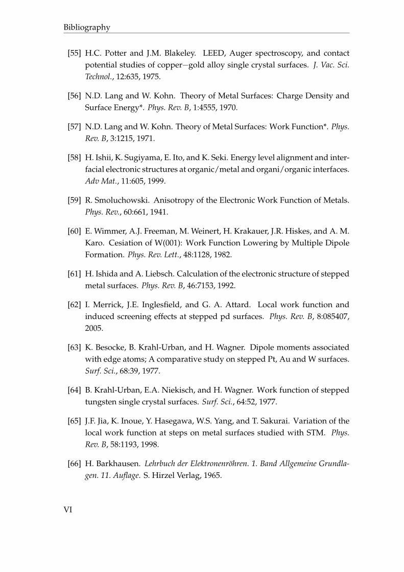
Bibliography
[55] H.C. Potter and J.M. Blakeley. LEED, Auger spectroscopy, and contactpotential studies of copper−gold alloy single crystal surfaces. J. Vac. Sci.Technol., 12:635, 1975.
[56] N.D. Lang and W. Kohn. Theory of Metal Surfaces: Charge Density andSurface Energy*. Phys. Rev. B, 1:4555, 1970.
[57] N.D. Lang and W. Kohn. Theory of Metal Surfaces: Work Function*. Phys.Rev. B, 3:1215, 1971.
[58] H. Ishii, K. Sugiyama, E. Ito, and K. Seki. Energy level alignment and inter-facial electronic structures at organic/metal and organi/organic interfaces.Adv Mat., 11:605, 1999.
[59] R. Smoluchowski. Anisotropy of the Electronic Work Function of Metals.Phys. Rev., 60:661, 1941.
[60] E. Wimmer, A.J. Freeman, M. Weinert, H. Krakauer, J.R. Hiskes, and A. M.Karo. Cesiation of W(001): Work Function Lowering by Multiple DipoleFormation. Phys. Rev. Lett., 48:1128, 1982.
[61] H. Ishida and A. Liebsch. Calculation of the electronic structure of steppedmetal surfaces. Phys. Rev. B, 46:7153, 1992.
[62] I. Merrick, J.E. Inglesfield, and G. A. Attard. Local work function andinduced screening effects at stepped pd surfaces. Phys. Rev. B, 8:085407,2005.
[63] K. Besocke, B. Krahl-Urban, and H. Wagner. Dipole moments associatedwith edge atoms; A comparative study on stepped Pt, Au and W surfaces.Surf. Sci., 68:39, 1977.
[64] B. Krahl-Urban, E.A. Niekisch, and H. Wagner. Work function of steppedtungsten single crystal surfaces. Surf. Sci., 64:52, 1977.
[65] J.F. Jia, K. Inoue, Y. Hasegawa, W.S. Yang, and T. Sakurai. Variation of thelocal work function at steps on metal surfaces studied with STM. Phys.Rev. B, 58:1193, 1998.
[66] H. Barkhausen. Lehrbuch der Elektronenrohren. 1. Band Allgemeine Grundla-gen. 11. Auflage. S. Hirzel Verlag, 1965.
VI
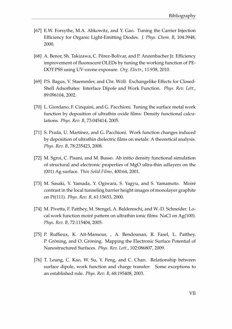
Bibliography
[67] E.W. Forsythe, M.A. Abkowitz, and Y. Gao. Tuning the Carrier InjectionEfficiency for Organic Light-Emitting Diodes. J. Phys. Chem. B, 104:3948,2000.
[68] A. Benor, Sh. Takizawa, C. Perez-Bolıvar, and P. Anzenbacher Jr. Efficiencyimprovement of fluorescent OLEDs by tuning the working function of PE-DOT:PSS using UV-ozone exposure. Org. Electr., 11:938, 2010.
[69] P.S. Bagus, V. Staemmler, and Chr. Woll. Exchangelike Effects for Closed-Shell Adsorbates: Interface Dipole and Work Function. Phys. Rev. Lett.,89:096104, 2002.
[70] L. Giordano, F. Cinquini, and G. Pacchioni. Tuning the surface metal workfunction by deposition of ultrathin oxide films: Density functional calcu-lations. Phys. Rev. B, 73:045414, 2005.
[71] S. Prada, U. Martinez, and G. Pacchioni. Work function changes inducedby deposition of ultrathin dielectric films on metals: A theoretical analysis.Phys. Rev. B, 78:235423, 2008.
[72] M. Sgroi, C. Pisani, and M. Busso. Ab initio density functional simulationof structural and electronic properties of MgO ultra-thin adlayers on the(001) Ag surface. Thin Solid Films, 400:64, 2001.
[73] M. Sasaki, Y. Yamada, Y. Ogiwara, S. Yagyu, and S. Yamamoto. Moirecontrast in the local tunneling barrier height images of monolayer graphiteon Pt(111). Phys. Rev. B, 61:15653, 2000.
[74] M. Pivetta, F. Patthey, M. Stengel, A. Baldereschi, and W.-D. Schneider. Lo-cal work function moire pattern on ultrathin ionic films: NaCl on Ag(100).Phys. Rev. B, 72:115404, 2005.
[75] P. Ruffieux, K. Aıt-Mansour, , A. Bendounan, R. Fasel, L. Patthey,P. Groning, and O. Groning. Mapping the Electronic Surface Potential ofNanostructured Surfaces. Phys. Rev. Lett., 102:086807, 2009.
[76] T. Leung, C. Kao, W. Su, Y. Feng, and C. Chan. Relationship betweensurface dipole, work function and charge transfer: Some exceptions toan established rule. Phys. Rev. B, 68:195408, 2003.
VII
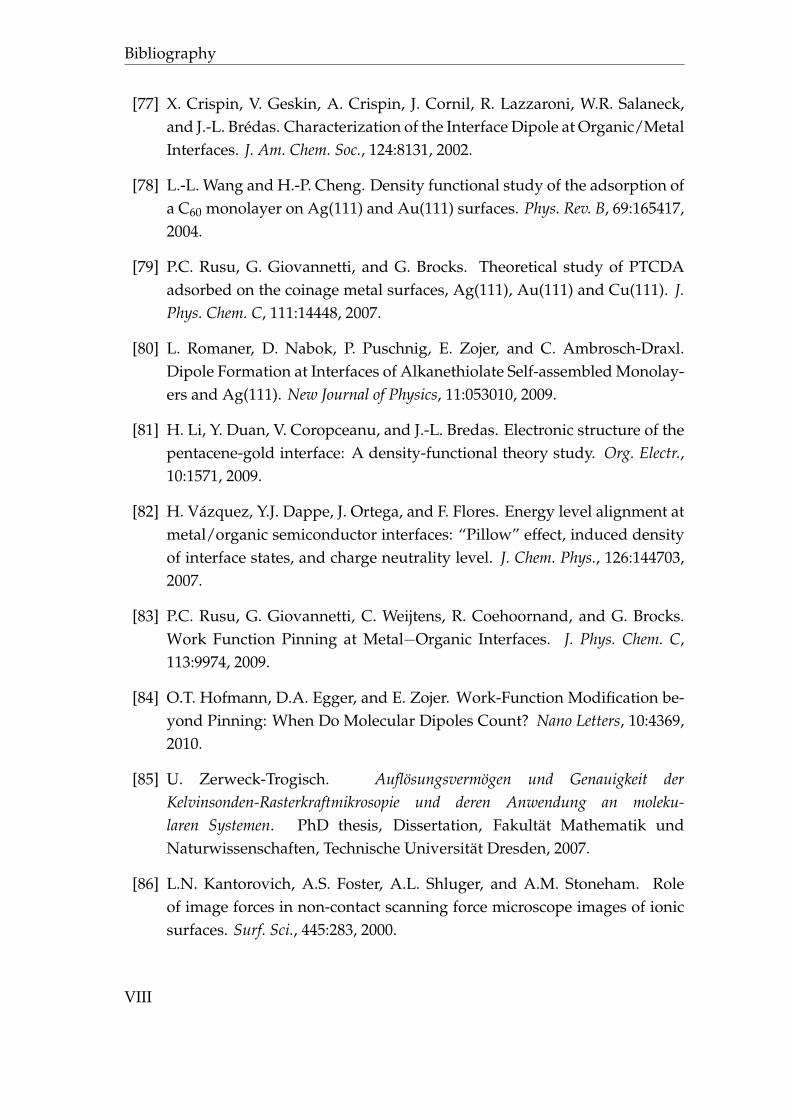
Bibliography
[77] X. Crispin, V. Geskin, A. Crispin, J. Cornil, R. Lazzaroni, W.R. Salaneck,and J.-L. Bredas. Characterization of the Interface Dipole at Organic/MetalInterfaces. J. Am. Chem. Soc., 124:8131, 2002.
[78] L.-L. Wang and H.-P. Cheng. Density functional study of the adsorption ofa C60 monolayer on Ag(111) and Au(111) surfaces. Phys. Rev. B, 69:165417,2004.
[79] P.C. Rusu, G. Giovannetti, and G. Brocks. Theoretical study of PTCDAadsorbed on the coinage metal surfaces, Ag(111), Au(111) and Cu(111). J.Phys. Chem. C, 111:14448, 2007.
[80] L. Romaner, D. Nabok, P. Puschnig, E. Zojer, and C. Ambrosch-Draxl.Dipole Formation at Interfaces of Alkanethiolate Self-assembled Monolay-ers and Ag(111). New Journal of Physics, 11:053010, 2009.
[81] H. Li, Y. Duan, V. Coropceanu, and J.-L. Bredas. Electronic structure of thepentacene-gold interface: A density-functional theory study. Org. Electr.,10:1571, 2009.
[82] H. Vazquez, Y.J. Dappe, J. Ortega, and F. Flores. Energy level alignment atmetal/organic semiconductor interfaces: “Pillow” effect, induced densityof interface states, and charge neutrality level. J. Chem. Phys., 126:144703,2007.
[83] P.C. Rusu, G. Giovannetti, C. Weijtens, R. Coehoornand, and G. Brocks.Work Function Pinning at Metal−Organic Interfaces. J. Phys. Chem. C,113:9974, 2009.
[84] O.T. Hofmann, D.A. Egger, and E. Zojer. Work-Function Modification be-yond Pinning: When Do Molecular Dipoles Count? Nano Letters, 10:4369,2010.
[85] U. Zerweck-Trogisch. Auflosungsvermogen und Genauigkeit derKelvinsonden-Rasterkraftmikrosopie und deren Anwendung an moleku-laren Systemen. PhD thesis, Dissertation, Fakultat Mathematik undNaturwissenschaften, Technische Universitat Dresden, 2007.
[86] L.N. Kantorovich, A.S. Foster, A.L. Shluger, and A.M. Stoneham. Roleof image forces in non-contact scanning force microscope images of ionicsurfaces. Surf. Sci., 445:283, 2000.
VIII
Bibliography
[87] W.A. Hofer, A.S. Foster, and A.L. Shluger. Theories of scanning probemicroscopes at the atomic scale. Rev. Mod. Phys., 75:1287, 2003.
[88] L. Nony, A. Foster, F. Bocquet, and Ch. Loppacher. Understanding theAtomic-Scale Contrast in Kelvin Probe Force Microscopy. Phys. Rev. Lett.,103:036802, 2009.
[89] L. Nony, F. Bocquet, Ch. Loppacher, and Th. Glatzel. On the relevanceof the atomic-scale contact potential difference by amplitude-modulationand frequency-modulation Kelvin probe force microscopy. Nanotechn.,20:264014, 2009.
[90] V.K. Wadhawan. Introduction to Ferroic Materials. Gordon and Breach Sci-ence Publishers, 2000.
[91] J. Valasek. Piezo-Electric and Allied Phenomena in Rochelle Salt. Phys.Rev., 17:475, 1921.
[92] N. Setter, D. Damjanovic, L.M. Eng, G. Fox, S. Gevorgian, S. Hong,A. Kingon, N.Y. Park, G.B. Stephenson, I. Stolichnov, A.K. Tagantsev, D.V.Taylor, T. Yamada, and S. Streiffer. Ferroelectric thin films: Review of ma-terials, properties, and applications. J. Appl. Phys., 5:051606, 2006.
[93] A.F. Devonshire. Theory of ferroelectrics. Adv. Phys., 3:85, 1954.
[94] J.F. Scott. Ferroelectric Memories. Springer-Verlag, Berlin Heidelberg New-York, 2000.
[95] S.L. Miller and P.J. McWorther. Physics of the ferroelectric nonvolatilememory field effect transistor. J. Appl. Phys., 72:5999, 1992.
[96] S.V. Kalinin and D.A. Bonnell. Screening Phenomena on Oxide Surfacesand Its Implications for Local Electrostatic and Transport Measurements.Nano Lett., 4:555, 2004.
[97] T.W. Kelley and C.D. Frisbie. Point contact current–voltage measurementson individual organic semiconductor grains by conducting probe atomicforce microscopy. J. Vac. Sci. Technol. B, 18:632, 2000.
[98] A.B. Chwang and C.D. Frisbie. Field Effect Transport Measurements onSingle Grains of Sexithiophene: Role of the Contacts. J. Phys. Chem. B,104:12202, 2000.
IX
Bibliography
[99] Th. Glatzel, L. Zimmerli, S. Koch, S. Kawai, and E. Meyer. Molecular as-semblies grown between metallic contacts on insulating surfaces. Appl.Phys. Lett., 94:063303, 2009.
[100] L. Gross, R.R. Schlittler, G. Meyer, L.-A. Fendt, F. Diederich, Th. Glatzel,S. Kawai, S. Koch, and E. Meyer. Contacting self-ordered molecular wiresby nanostencil lithography. J. Vac. Sc. Technol. B, 28:C4D34, 2010.
[101] G. Horowitz. Organic field-effect transistors. Adv. Mat., 10:365, 1998.
[102] C.D. Dimitrakopoulos and P.R.L. Malenfant. Organic thin film transistorsfor large area electronics. Adv. Mat., 14:99, 2002.
[103] T. Mori. Molecular materials for organic field-effect transistors. J. Phys.:Cond. Mat., 20:184010, 2008.
[104] W. Silveira and J. Marohn. Microscopic View of Charge Injection in anOrganic Semiconductor. Phys. Rev. Lett., 93:116104, 2004.
[105] S.G.J Mathijssen, M. Colle, A.J.G. Mank, M. Kemerink, P.A. Bobbert, andD.M. de Leeuw. Scanning Kelvin probe microscopy on organic field-effecttransistors during gate bias stress. Appl. Phys. Lett., 90:192104, 2007.
[106] S. Ikeda, T. Shimada, M. Kiguchi, and K. Saiki. Visualization of inducedcharge in an organic thin-film transistor by cross-sectional potential map-ping. J. Appl. Phys., 101:094509, 2007.
[107] Y. Luo, F. Gustavo, J.-Y. Henry, F. Mathevet, F. Lefloch, M. Sanquer, P. Ran-nou, and B. Grevin. Probing Local Electronic Transport at the OrganicSingle-Crystal/Dielectric Interface. Adv. Mat., 19:2267, 2007.
[108] R. Scholz, D. Lehmann, A.-D. Muller, F. Muller, and D.R.T. Zahn. Poten-tiometry on pentacene OFETs: Charge carrier mobilities and injection bar-riers in bottom and top contact configurations. phys. stat. sol. (a), 205:591,2008.
[109] T. Miyazaki, K. Kobayashi, K. Ishida, S. Hotta, T. Horiuchi, K. Matsushige,and H. Yamada. Increase in carrier mobility of organic ultrathin-film tran-sistor with increasing molecular layers investigated by Kelvin probe forcemicroscopy. J. Appl. Phys., 97:124503, 2005.
X
Bibliography
[110] T.W. Kelley and C.D. Frisbie. Gate Voltage Dependent Resistance of a Sin-gle Organic Semiconductor Grain Boundary. J. Phys. Chem. B, 105:4538,2001.
[111] K.P. Puntambekar, P.V. Pesavento, and C.D. Frisbie. Surface potential pro-filing and contact resistance measurements on operating pentacene thin-film transistors by Kelvin probe force microscopy. Appl. Phys. Lett., 83:5539,2003.
[112] L.C. Teague, B.H. Hamadani, O.D. Jurchescu, S. Subramanian, J.E. An-thony, T.N. Jackson, C.A. Richter, D.J. Gundlach, and J.G. Kushmerick.Surface Potential Imaging of Solution Processable Acene-Based Thin FilmTransistors. Adv. Mat., 20:4513, 2008.
[113] Ch. Loppacher. Nichtkontakt-Rasterkraftmikroskopie mit digitalem Phasen-regelkreis. PhD thesis, Philosophisch-Naturwissenschaftliche Fakultat,Universitat Basel, 2000.
[114] J.V. Barth, H. Brune, G. Ertl, and R.J. Behm. Scanning tunneling mi-croscopy observations on the reconstructed Au(111) surface: Atomic struc-ture, long-range superstructure, rotational domains, and surface defects.Phys. Rev. B, 42:9307, 1990.
[115] S. Sadewasser, C. Leendertz, F. Streicher, and M.Ch. Lux-Steiner. The influ-ence of surface topography on Kelvin probe force microscopy. Nanotech.,20:505503, 2009.
[116] J.C. Heyraud and J.J. Metois. Anomalous 422 diffraction spots from 111 flatgold crystallites: (111) surface reconstruction and moire fringes betweenthe surface and the bulk. Surf. Sci., 100:519, 1980.
[117] K. Takayanagi, Y. Tanishiro, K. Yagi, K. Kobayashi, and G. Honjo. UHV-TEM study on the reconstructed surface of Au(111): Metastable p′′ × p′′and stable p× 1 surface structure. Surf. Sci., 205:637, 1988.
[118] K.G. Huang, D. Gibbs, D.M. Zehner, A.R. Sandy, and S.G.J. Mochrie. Phasebehavior of the Au(111) surface: Discommensurations and kinks. Phys.Rev. Lett., 65:3313, 1990.
XI
Bibliography
[119] U. Harten, A.M. Lahee, J.P. Toennies, and Ch. Woll. Observation of a Soli-ton Reconstruction of Au(111) by High-Resolution Helium-Atom Diffrac-tion. Phys. Rev. Lett., 54:2619, 1985.
[120] W. Haiss. Surface stress of clean and adsorbate-covered solids. Rep. Prog.Phys., 64:591, 2001.
[121] C.E. Bach, M. Giesen, H. Ibach, and T.L. Einstein. Stress Relief in Recon-struction. Phys. Rev. Lett., 78:4225, 1997.
[122] H. Bulou and C. Goyhenex. Local strain analysis of the herringbone recon-struction of Au(111) through atomistic simulations. Phys. Rev. B, 65:045407,2002.
[123] F.C. Frank. Physica (Amsterdam), 15:131, 1949.
[124] J.P. Hirth and J. Lothe. Theory of Dislocations. Malabar, Fla. : Krieger, 1992.
[125] N. Takeuchi, C.T. Chan, and K.M. Ho. Au(111): A theoretical study of thesurface reconstruction and the surface electronic structure. Phys. Rev. B,43:13899, 1991.
[126] W. Chen, V. Madhavan, T. Jamneala, and M.F. Crommie. Scanning Tunnel-ing Microscopy Observation of an Electronic Superlattice at the Surface ofClean Gold. Phys. Rev. Lett., 80:1469, 1998.
[127] L. Burgi, H. Brune, and K. Kern. Imaging of Electron Potential Landscapeson Au(111). Phys. Rev. Lett., 89:176801, 2002.
[128] S. Molitor, P. Guthner, and T. Berghaus. Contrast inversion in dynamicforce microscopy on silicon (111) 7× 7 and gold (111) 23×
√3. Appl. Surf.
Sc., 140:276, 1999.
[129] J.M. Mativetsky, S.A. Burke, R. Hoffmann, Y. Sun, and P. Grutter. Molec-ular resolution imaging of C60 on Au(111) by non-contact atomic forcemicroscopy. Nanotech., 15:S40, 2004.
[130] D.D. Chambliss, R.J. Wilson, and S. Chiang. Nucleation of ordered Niisland arrays on Au(111) by surface-lattice dislocations. Phys. Rev. Lett.,66:1721, 1991.
XII
Bibliography
[131] S. Padovani, I. Chado, F. Scheurer, and J.P. Bucher. Transition from zero-dimensional superparamagnetism to two-dimensional ferromagnetism ofCo clusters on Au(111). Phys. Rev. B, 59:11887, 1999.
[132] M. Hohage, Th. Michely, and George Comsa. Pt(111) network reconstruc-tion: structure, growth and decay. Surf. Sc., 337:249, 1995.
[133] M. Bott, M. Hohage, Th. Michely, and George Comsa. Pt(111) reconstruc-tion induced by enhanced pt gas-phase chemical potential. Phys. Rev. Lett.,70:1489, 1993.
[134] J. Engbæk, J. Schiøtz, B. Dahl-Madsen, and S. Horch. Atomic structureof screw dislocations intersecting the Au(111) surface: A combined scan-ning tunneling microscopy and molecular dynamics study. Phys. Rev. B,74:195434, 2006.
[135] D. Fichou. Structural order in conjugated oligothiophenes and its implica-tions on opto-electronic devices. J. Mat. Chem., 10:571, 2000.
[136] T. Schwieger, X. Liu, H. Peisert, B. Adolphi, N. Kiriy, and M. Knupfer.Electronic properties of interfaces between different sexithiophenes andgold. J. Appl. Phys., 97:123712, 2005.
[137] M. Kiel, K. Duncker, Ch. Hagendorf, and W. Widdra. Molecular structureand chiral separation in alpha-sexithiophene ultrathin films on Au(111):Low-energy electron diffraction and scanning tunneling microscopy. Phys.Rev. B, 75:195439, 2007.
[138] A.J. Makinen, J.P. Long, N.J. Watkins, and Z.H. Kafafi. Sexithiophene Ad-layer Growth on Vicinal Gold Surfaces. J. Phys. Chem. B, 109:5790, 2005.
[139] H. Glowatzki, S. Duhm, K.-F. Braun, J.P. Rabe, and N. Koch. Molecularchains and carpets of sexithiophenes on Au(111). Phys. Rev. B, 76:125425,2007.
[140] E. Varene, I. Martin, and P. Tegeder. Optically Induced Inter- and Intrafa-cial Electron Transfer Probed by Two-Photon Photoemission: ElectronicStates of Sexithiophene on Au(111). J. Phys. Chem. Lett., 2:252, 2011.
[141] A. Ogunsipe, J.-Y. Chen, and T. Nyokong. Photophysical and photochem-ical studies of zinc(ii) phthalocyanine derivatives: effects of substituentsand solvents. New J. Chem, 28:822, 2004.
XIII
Bibliography
[142] M. Koudia, M. Abel, Ch. Maurel, A. Bliek, D. Catalin, M. Mossoyan, J.-Ch.Mossoyan, and L. Porte. Influence of Chlorine Substitution on the Self-Assembly of Zinc Phthalocyanine. J. Phys. Chem. B, 110:10058, 2006.
[143] M. Koudia, M. Abel, Ch. Maurel, A. Bliek, D. Catalin, M. Mossoyan, J.-Ch.Mossoyan, and L. Porte. First-principle study of the hydrogen bonds in athin film of phthalocyanine molecules. Surf. Sc., 601:1040, 2007.
[144] P. Amsalem, L. Giovanelli, J. Themlin, M. Koudia, M. Abel, V. Oison,Y. Ksari, M. Mossoyan, and L. Porte. Interface formation and growth of athin film of ZnPcCl8/Ag(111) studied by photoelectron spectroscopy. Surf.Sc., 601:4185, 2007.
[145] M. Abel, V. Oison, M. Koudia, C. Maurel, C. Katan, and L. Porte. Design-ing a New Two-Dimensional Molecular Layout by Hydrogen Bonding.ChemPhysChem, 7:82, 2006.
[146] V. Oison, M. Koudia, M. Abel, and L. Porte. Influence of stress onhydrogen-bond formation in a halogenated phthalocyanine network.Phys. Rev. B, 75:035428, 2007.
[147] P. Milde, U. Zerweck, L.M. Eng, M. Abel, L. Giovanelli, L. Nony,M. Mossoyan, L. Porte, and Ch. Loppacher. Interface dipole formationof different znpccl8 phases on Ag(111) observed by Kelvin probe force mi-croscopy. Nanotech., 19:305501, 2008.
[148] Ch.-W. Chen, P.-Y. Hsieh, H.-H. Chiang, Ch.-L. Lin, H.-M. Wu, and Ch.-Ch.Wu. Top-emitting organic light-emitting devices using surface-modifiedAg anode. Appl. Phys. Lett., 83:5127, 2003.
[149] Y.C. Chen, J.E. Cunningham, and C.P. Flynn. Dependence of rare-gas-adsorbate dipole moment on substrate work function. Phys. Rev. B,30:7317, 1984.
[150] M. Iwamoto and E. Itoh. Nano-electrostatic phenomena in Langmuir-Blodgett films. Thin Solid Films, 331:15, 1998.
[151] G.H. Enevoldsen, T. Glatzel, M.C. Christensen, J.V. Lauritsen, and F. Besen-bacher. Atomic Scale Kelvin Probe Force Microscopy Studies of the SurfacePotential Variations on the Tio2(110) Surface. Phys. Rev. Lett., 100:236104,2008.
XIV
Bibliography
[152] J.L. Moll and Y. Tarui. A New Solid State Memory Resistor. IEEE Trans.Electron Devices, 10:338, 1963.
[153] Y. Watanabe. Theoretical stability of the polarization in insulating ferro-electric/semiconductor structures. J. Appl. Phys., 83:2179, 1998.
[154] G. Velu, C. Legrand, O. Tharaud, A. Chapoton, D. Remiens, andG. Horowitz. Low driving voltages and memory effect in organic thin-film transistors with a ferroelectric gate insulator. Appl. Phys. Lett., 79:659,2001.
[155] M. Egginger, S. Bauer, R. Schwodiauer, H. Neugebauer, and N.S. Sariciftci.Current versus gate voltage hysteresis in organic field effect transistors.Monatsh. Chem., 140:735, 2009.
[156] K.N.N. Unni, R. de Bettignies, S. Dabos-Seignon, and J.M. Nunzi. A non-volatile memory element based on a quaterthiophene field-effect transis-tor. Mat. Lett., 59:1165, 2005.
[157] R. Tamura, E. Lim, T. Manaka, and M. Iwamoto. Analysis of pentacenefield effect transistor as a Maxwell-Wagner effect element. J. Appl. Phys.,100:114515, 2006.
[158] B. Jaffe, W.R. Cook, and H. Jaffe. Piezoelectric Ceramics. Academic Press,London, 1971.
[159] A.L. Roytburd, S.P. Alpay, L.A. Bendersky, V. Nagarajan, and R. Ramesh.Three-domain architecture of stress-free epitaxial ferroelectric films. J.Appl. Phys., 89:553, 2001.
[160] T. Tybell, C.H. Ahn, and J.-M. Triscone. Ferroelectricity in thin perovskitefilms. Appl. Phys. Lett., 75:856, 1999.
[161] N. Pertsev, V. Kukhar, H. Kohlstedt, and R. Waser. Phase diagrams andphysical properties of single-domain epitaxial Pb(Zr1-xTix)O3 thin films.Phys. Rev. B, 67:054107, 2003.
[162] J.S. Speck and W. Pompe. Domain configurations due to multiple misfitrelaxation mechanisms in epitaxial ferroelectric thin films. II. Theory. J.Appl. Phys., 75:466, 1994.
XV
Bibliography
[163] Jorge Cors: sales represantative at Phasis Sarl. Private communication.
[164] J. Wooldridge, J.F. Blackburn, N.L. McCartney, M. Stewart, P. Weaver, andM.G. Cain. Small-scale piezoelectric devices: Pyroelectric contributions tothe piezoelectric response. J. Appl. Phys., 107:104118, 2010.
[165] L. Pintilie, I. Vrejoiu, D. Hesse, G. LeRhun, and M. Alexe. Extrinsic contri-butions to the apparent thickness dependence of the dielectric constant inepitaxial Pb(Zr,Ti)O3 thin films. Phys. Rev. B, 75:224113, 2007.
[166] Y. Watanabe, M. Okano, and A. Masuda. Surface Conduction on InsulatingBaTiO3 Crystal Suggesting an Intrinsic Surface Electron Layer. Phys. Rev.Lett., 86:332, 2001.
[167] C.S. Ganpule, V. Nagarajan, H. Li, A.S. Ogale, D.E. Steinhauer, S. Aggar-wal, E. Williams, R. Ramesh, and P. De Wolf. Role of 90°domains in leadzirconate titanate thin films. Appl. Phys. Lett., 77:292, 2000.
[168] Y.L. Li, S.Y. Hu, Z.K. Liu, and L.Q. Chen. Effect of electrical boundaryconditions on ferroelectric domain structures in thin films. Appl. Phys. Lett.,81:427, 2002.
[169] Y.L. Li, S.Y. Hu, and L.Q. Chen. Ferroelectric domain morphologies of(001) PbZr1-xTixO3 epitaxial thin films. J. Appl. Phys., 97:034112, 2005.
[170] T. Kodzasa, M. Yoshida, S. Uemura, and T. Kamata. Memory effects ofpentacene MFS-FET. Synth. Met., 137:943, 2003.
[171] B. Stadlober, M. Zirkl, G. Leising, N. Gaar, I. Graz, S. Bauer-Gogonea, andS. Bauer. Transparent Pyroelectric Sensors and Organic Field-effect Tran-sistors with Fluorinated Polymers: Steps towards Organic Infrared Detec-tors. IEEE Trans. Dielectr. Electr. Ins., 13:1087, 2006.
[172] G.H. Gelinck, A.W. Marsman, F.J. Touwslager, S. Setayesh, D.M. de Leeuw,R.C.G. Naber, and P.W.M. Blom. All-polymer ferroelectric transistors.Appl. Phys. Lett., 87:092903, 2005.
[173] R.C.G. Naber, C. Tanase, P.W.M. Blom, G.H. Gelinck, A.W. Marsman, F.J.Touwslager, S. Setayesh, and D.M. de Leeuw. High-performance solution-processed polymer ferroelectric field-effect transistors. Nat. Mat., 4:243,2005.
XVI
Bibliography
[174] J.C. Scott and L.D. Bozano. Nonvolatile Memory Elements Based on Or-ganic Material. Adv. Mat., 19:1452, 2007.
[175] P. Kim, S.C. Jones, P.J. Hotchkiss, J.N. Haddock, B. Kippelen, S.R. Marder,and J.W. Perry. Phosphonic Acid-Modified Barium Titanate PolymerNanocomposites with High Permittivity and Dielectric Strength. Adv.Mat., 19:1001, 2007.
[176] K. Haubner, E. Jaehne, H.-J.P. Adler, D. Koehler, C. Loppacher, L.M. Eng,J. Grenzer, A. Herasimovich, and S. Scheinert. Assembly, structure, andperformance of an ultra-thin film organic field-effect transistor (OFET)based on substituted oligothiophenes. phys. stat. sol. (a), 205:430, 2008.
[177] R. Luschtinetz, J. Frenzel, Th. Milek, and G. Seifert. Adsorption of Phos-phonic Acid at the TiO2 Anatase (101) and Rutile (110) Surfaces. J. Phys.Chem. C, 113:5730, 2009.
[178] Dr. Andreas Koitzsch at the Leibniz-Institut fur Festkorper-und Werkstoff-forschung Dresden. Private communication 08.09.2010.
[179] J. Sader and S.P. Jarvis. Interpretation of frequency modulation atomicforce microscopy in terms of fractional calculus. Phys. Rev. B, 70:012303,2004.
[180] G.M. Steeves. Junction Mixing Scanning Tunneling Microscopy. PhD thesis,Department of Physics, University of Alberta, 2001.
[181] N. Balke, I. Bdikin, S.V. Kalinin, and A.L. Kholkin. ElectromechanicalImaging and Spectroscopy of Ferroelectric and Piezoelectric Materials:State of the Art and Prospects for the Future. J. Am. Ceram. Soc., 92:1629,2009.
XVII


Acknowledgement
In the field of observation, chance favors only the pre-pared mind.
Louis Pasteur
I wish to give thank to all the people who supported me during the work onthis thesis.
First, I thank Prof. Lukas M. Eng for the possibility to work in the SPM2-group and on this thesis. Thank you for the huge scientific freedom and constantsupport of my work I could experience in the past years.
I want to thank Prof. Christian Loppacher for being the second referee ofthis work. I want to thank you for guiding me into the field of scanning probemicroscopy and for sharing your knowledge with me.
As constant backup at any kind of problem in the lab, I thank Dr. UlrichZerweck-Trogisch. Without your practical knowledge, ideas and willingness forcontinuous improvements of the mammoth many of the experiments in this the-sis would have stayed impossible.
Furthermore, I wish to thank Dr. Kinga Haubner, who provided me withchemistry, and all collaborators of the FerroFET work group for stimulatingdiscussions. For the continuous help with X-ray photoelectron measurementsI want to thank Dr. Andreas Koitzsch and Rico Schonfelder. Speaking aboutsamples, I thank Dr. Jochen Grebing for his patient work on small structures.
Equally important for the work were all the little ideas, questions, discussionsand jokes which create such a pleasant and stimulating atmosphere in the SPM2-group. Thank you all for the great time. Especially, I want to name Dr. Oliver Mi-eth, Dr. Denny Kohler and Vera Hofmann who share room and spirit of BEY136.As it comes to rooms, I thank all coworkers in the Bey99/100 for practical helpand your considerateness when it came to sensitive measurements. As a head-stone for successive work with any kind of electronics I wish to thank Ralf Rau-pach. Further I thank Andreas Hille for his help with some numerics and Dr.
XIX

Acknowledgement
Sebastian Teich as well as Dr. Stefan Grafstrom for X-ray photoelectron mea-surements.
I wish to thank Vera Hofmann and Jan Murawski who both contributed withtheir work. I hope you had an equally good time as diploma students as I hadas your advisor.
Also, I want to thank all the people in the Institute for Applied Photophysicsfor the pleasant atmosphere. It was a great time working here.
I thank all my friends. You kept me up in hard times and gave me joy in thegood times we had together – playing table soccer, catching fish, brewing beer,listening to whispered poetry, traveling around, and ... it is a much too long listto name everything.
Last but not least, I thank my parents and family for all the support during allthe years. Without your care, help, and motivation I would never have come sofar. Thank you.
XX
Abbreviations and Symbols
CPD contact potential differenceLCPD local contact potential difference
SPM scanning probe microscopySTM scanning tunnelling microscopyAFM atomic force microscopync-AFM non-contact atomic force microscopyKPFM Kelvin probe force microscopyPFM piezoresponse force microscopyPLL phase-locked loopUHV ultra-high vacuum
DB6T β,β′-dibutyl sexithiopheneα-6T α-sexithiopheneZnPcCl8 2,3,9,10,16,17,23,24-octachloro zinc phthalocyanineCnBtPA 5-cyano-2-(butyl-4-phosphonic acid)-3-butyl thiopheneDCnDB4T α,ω-dicyano substituted-β,β′-dibutyl quaterthiophenePZT lead zirconate titanateSTO strontium titanateSRO strontium ruthanateTiOx titanium oxide
Evl vacuum levelEvx vacuum level of object xEFx Fermi level of object xφx work function of object x
XXI

Abbreviations and Symbols
e elementary chargee− electronQ charge
~Fts tip sample interaction force~Fel electrostatic forceAexc excitation amplitudeAi oscillation amplitude of the ith cantilever modeϕi oscillation phase of the ith cantilever modeA oscillation amplitude in experimentω mechanical drive frequencyωi ith cantilever mode eigenfrequencyωres,i ith cantilever mode disturbed resonance frequency∆ωi ith cantilever mode frequency shiftki ith cantilever mode force constantQi ith cantilever mode quality factorτi ith cantilever mode damping constantz tip positionz0 tip equilibrium position
Udc dc-bias between tip and sampleU∗dc contact potential: dc-bias applied by the Kelvin controller∆U∗dc,xy difference in the contact potential between area x and yU∗dc,stat dc-bias, that minimizes the static frequency shiftU∗dc,AM dc-bias, that minimizes Aωm
U∗dc,FM dc-bias, that minimizes ζωm
Ucpd contact potential difference given by the difference in work functionUlcpd local contact potential difference between tip and sampleUm Kelvin modulation voltage between tip and sampleum amplitude of the Kelvin modulation voltageωm frequency of the Kelvin modulation voltageC tip-sample capacitance∆ωstat.0 static shift of the fundamental eigenfrequency
XXII

Aωm amplitude of the driven oscillation atωmA2ωm amplitude of the driven oscillation at 2ωmζωm magnitude of the sidebands atωmζ2ωm magnitude of the sidebands at 2ωm
℘ surface dipole densityn positive charge background densityn(z) electron densityε0 permittivity of free spaceρ differential charge densityσ surface charge densityd dipole lengthR radius
Ueff effective electrostatic interaction potentialu1 electrostatic charge electrode interaction potentialu2 electrostatic charge charge interaction potential
UP ferroelectric surface potentialdf thickness of ferroelectric layerPzr remanent polarisation perpendicular to the surfaceσS screening charge densityε dielectric constantd closest tip-sample separationϕel electrostatic potential
Q chargel dipole lengthd step atom distancep dipole moment
ρct density of transferred chargeσct surface density of transferred charge
XXIII

Abbreviations and Symbols
℘ct charge transfer dipole densityh heightheff effective height
ωr repetition frequency of the pumpTr repetition period of the pump2τ on-time of the probe pulse2ϕτ on-time phase increment of the probe pulsetd delay time of the probe pulseϕd delay phase of the probe pulse
dij piezoelectric tensorT mechanical stress tensorS mechanical strain tensorE electric field
XXIV
List of Figures
1.1 The voltaic pile . . . . . . . . . . . . . . . . . . . . . . . . . . . . . 41.2 The experiment of Lord Kelvin . . . . . . . . . . . . . . . . . . . . 61.3 The contact potential difference . . . . . . . . . . . . . . . . . . . . 71.4 Modulated cantilever spectrum . . . . . . . . . . . . . . . . . . . . 13
2.1 The jellium model . . . . . . . . . . . . . . . . . . . . . . . . . . . . 202.2 The vacuum level . . . . . . . . . . . . . . . . . . . . . . . . . . . . 222.3 The local vacuum level around a dipole density . . . . . . . . . . 242.4 Effects with impact on the work function . . . . . . . . . . . . . . 272.5 Kelvin probe force microscopy on ferroelectric thin films . . . . . 31
4.1 Stepped Au(111) surface . . . . . . . . . . . . . . . . . . . . . . . . 404.2 Schematic of the Au(111)-(22×
√3)-reconstruction . . . . . . . . . 43
4.3 The Au(111)-(22×√
3)-reconstruction . . . . . . . . . . . . . . . . 444.4 Au(111)-(22×
√3) local contact potential . . . . . . . . . . . . . . 45
4.5 Au(111) with another type of surface reconstruction . . . . . . . . 474.6 Contact potential of the Au(111) dot pattern . . . . . . . . . . . . . 494.7 Au(111) reconstruction networks . . . . . . . . . . . . . . . . . . . 50
5.1 Chemical structure of β,β′-dibutyl sexithiophene . . . . . . . . . 545.2 DB6T on Au(111) . . . . . . . . . . . . . . . . . . . . . . . . . . . . 565.3 Schematic drawing of three structural ZnPcCl8 phases . . . . . . . 585.4 Comparison between ZnPcCl8 phases P1 and P2 . . . . . . . . . . 605.5 Comparison between ZnPcCl8 phases P2 and P3 . . . . . . . . . . 625.6 ZnPcCl8 islands on Ag(111) . . . . . . . . . . . . . . . . . . . . . . 645.7 ZnPcCl8-island in phase P4 . . . . . . . . . . . . . . . . . . . . . . 655.8 Disordered ZnPcCl8 islands . . . . . . . . . . . . . . . . . . . . . . 685.9 ZnPcCl8 molecular resolved contact potential . . . . . . . . . . . . 69
6.1 Properties of lead zirconate titanate . . . . . . . . . . . . . . . . . . 746.2 Comparison of 50 nm and 100 nm PZT thin films on STO . . . . . 77
XXV
List of Figures
6.3 Comparison of pristine and cleaned 20 nm PZT thin films on STO 796.4 The effect of the PZT cleaning procedure . . . . . . . . . . . . . . . 806.5 Domain patterns written in a 50 nm PZT thin film on STO . . . . 816.6 Temperature change of induced domain contrast on PZT . . . . . 826.7 Contact potential of switched domain patterns . . . . . . . . . . . 83
7.1 Chemical structure of 5-cyano-2-(butyl-4-phosphonic acid)-3-butyl thiophene . . . . . . . . . . . . . . . . . . . . . . . . . . . . . 88
7.2 50 nm PZT thin film with CnBtPA applied from solution . . . . . 907.3 CnBtPA dry deposition on TiOx . . . . . . . . . . . . . . . . . . . . 917.4 X-ray photoelectron spectrum of the TiOx/CnBtPA . . . . . . . . . 927.5 Chemical structure of α,ω-dicyano substituted-β,β′-dibutyl
quaterthiophene . . . . . . . . . . . . . . . . . . . . . . . . . . . . . 947.6 DCnDB4T on clean and CnBtPA buffered PZT . . . . . . . . . . . 957.7 Phase boundaries in DCnDB4T layers . . . . . . . . . . . . . . . . 96
8.1 Kelvin probe force approach curves on the Au(111) dot pattern . 1028.2 Photo voltage generated in the scanning tip . . . . . . . . . . . . . 105
A.1 Piezoresponse force microscopy . . . . . . . . . . . . . . . . . . . . 110
D.1 Stepped Au(111)-surface . . . . . . . . . . . . . . . . . . . . . . . . 120D.2 Survey - Au(111) surface with dot pattern . . . . . . . . . . . . . . 121D.3 Au(111) surface reconstructions . . . . . . . . . . . . . . . . . . . . 122D.4 Defects in the Au(111) dot pattern . . . . . . . . . . . . . . . . . . 123D.5 Disordered ZnPcCl8 island . . . . . . . . . . . . . . . . . . . . . . . 124D.6 Metal flakes on PZT . . . . . . . . . . . . . . . . . . . . . . . . . . . 125D.7 Survey - 50 nm and 100 nm PZT thin film on STO . . . . . . . . . 126D.8 Survey - pristine and dry cleaned PZT thin film . . . . . . . . . . . 127D.9 PZT thin film grown on SRO buffered STO . . . . . . . . . . . . . 128D.10 Survey - CnBtPA dry deposition . . . . . . . . . . . . . . . . . . . 129D.11 DCnDB4T - screw dislocation and molecular structure . . . . . . . 130D.12 Amorph DCnDB4T layer on clean PZT . . . . . . . . . . . . . . . . 131
XXVI


