Embed Size (px)
Citation preview
arX
iv:c
ond-
mat
/000
3258
v1 [
cond
-mat
.mes
-hal
l] 1
5 M
ar 2
000
Wavefronts may move upstream in semiconductor superlattices
A. CarpioDepartamento de Matematica Aplicada, Universidad Complutense, Madrid 28040, Spain.
L.L. BonillaDepartamento de Matematicas, Universidad Carlos III de Madrid, Avenida de la Universidad 30, 28911 Leganes, Spain
A. Wacker and E. SchollInstitut fur Theoretische Physik, Technische Universitat Berlin, Hardenbergstr. 36, 10623 Berlin, Germany
(February 6, 2008)
In weakly coupled, current biased, doped semiconductor superlattices, domain walls may moveupstream against the flow of electrons. For appropriate doping values, a domain wall separatingtwo electric field domains moves downstream below a first critical current, it remains stationarybetween this value and a second critical current, and it moves upstream above. These conclusionsare reached by using a comparison principle to analyze a discrete drift-diffusion model, and validatedby numerical simulations. Possible experimental realizations are suggested.
PACS numbers: 05.45.-a, 72.20Ht, 73.61.-r
I. INTRODUCTION
Current instabilities in doped semiconductor superlat-tices (SL) have been an active subject of research duringthis decade. For strongly coupled SL, Bloch oscillations[1–3] and Wannier-Stark hopping [4] produce negativedifferential conductivity (NDC) at high electric fields.This may result in self-sustained oscillations of the cur-rent due to recycling of charge dipole domains as in theGunn effect of bulk n-GaAs [5,2]. For weakly coupled SL,sequential tunneling is the main mechanism of verticaltransport. Under dc voltage bias conditions, stationaryelectric field domains may form if doping is large enough[6,7]. Below a critical doping value, the existing chargeinside the SL may not be able to pin domain walls, andcurrent self-oscillations appear [8,9]. These oscillationsmay be due to recycling of charge monopoles (domainwalls) or dipoles depending on the boundary conditionat the injecting contact region (in a typical n+-n-n+ con-figuration with the SL imbedded between highly dopedregions, the doping at the emitter region is crucial) [10].Driven chaotic oscillations have also been predicted [11]and observed in experiments [12]. Lastly, there are waysto tune the charge inside the SL (and therefore obtainstationary domains or self-oscillations) without replacingit by a different one. For example, by applying a trans-verse magnetic field [13] or by photoexciting the SL [14].
Transport in weakly coupled SL can be described bysimple rate equation models for electron densities andaverage fields in the wells, [15–18]. Many of the effectsrelated above have been explained by means of a simplediscrete drift model [16,17,19,20]. In this model, the tun-neling current between two adjacent wells, Ji→i+1, equalsthe 2D electron charge density at well i times a drift ve-locity, which depends on the electric field at the samewell. By starting from a microscopic sequential tunneling
model, it has been shown that the discrete drift model isa good approximation at low temperatures and for fieldsabove the first plateau of the SL current-voltage charac-teristic [18,21]. For low dc voltages on the first plateau,a discrete diffusion (which is a nonlinear function of thefield) should be added. This term contains the contri-bution to Ji→i+1 of the tunneling from well i + 1 backto well i (which vanishes for large enough electric fields)[18,21]. In this paper we report an interesting conse-quence of electron diffusivity at low fields: if the currentis sufficiently high, and so is the doping, a domain wall(monopole wave) which connects two domains may travelin a direction opposite to the flow direction for electrons(i.e., upstream, in the positive current direction!). Thisstriking phenomenon is contrary to the usual situation:a monopole either moves downstream (in the direction ofthe flow of electrons), or it remains stationary, [19]. Wesubstantiate our claim both by numerical simulations ofthe discrete drift-diffusion model and by rigorous mathe-matical analysis based upon a comparison principle [22].Mathematical analysis yields useful bounds for criticalvalues of current and well doping, and for monopole ve-locity.
There are related fields for which differential-differenceequations (similar to discrete drift-diffusion models)model the systems of interest. Well-known are propa-gation of nerve impulses along myelinated fibers, mod-elled by discrete FitzHugh-Nagumo equations [23,24],motion of dislocations [25,26] and sliding charge densitywaves [27], modelled by variants of the Frenkel-Kontorovamodel [28], etc. The theory of wavefront propagation hasbeen developed for some of these models, which are sim-pler than ours: convection is typically absent from themand diffusion is purely linear [24].
The rest of the paper is as follows. We write the drift-diffusion model with appropriate boundary conditions inSection II. There we render these equations dimension-
1
less and explain the results of numerical simulations ona current biased infinitely long SL. Furthermore, we findby numerical simulations that our results for infinite SLmay be realized in finite SL with appropriate boundaryconditions under constant current bias. The theoreticalanalysis based on the comparison principle is presented inSection III. Section IV contains our conclusions. Finallysome material of a more technical nature is relegated tothe Appendices.
II. DISCRETE DRIFT-DIFFUSION MODEL
A. Equations and boundary conditions
At low enough temperatures (much less than a typi-cal Fermi energy of a SL well measured from the firstsubband, say 20 meV or 232 K), the following discretedrift-diffusion equations model sequential vertical trans-port in a weakly doped SL [18,21]:
ε
e
dFi
dt+
niv(Fi)
d + w− D(Fi)
ni+1 − ni
(d + w)2= J(t) , (1)
Fi − Fi−1 =e
ε(ni − Nw
D). (2)
Eq. (1) is Ampere’s law establishig that the total currentdensity, eJ , is sum of displacement and tunneling cur-rents. The latter consists of a drift term, eniv(Fi)/(d +w), and a diffusion term, eD(Fi) (ni+1 − ni)/(d + w)2.We have adopted the convention (usual in this field) thatthe current density has the same direction as the flow ofelectrons. Eq. (1) holds for i = 1, . . . , N − 1. Eq. (2) isthe Poisson equation, and it holds for i = 1, . . . , N . ni isthe 2D electron number density at well i, which is singu-larly concentrated on a plane located at the end of thewell. Fi is minus an average electric field on a SL periodcomprising the ith well and the ith barrier (well i liesbetween barriers i − 1 and i: barriers 0 and N separatethe SL from the emitter and collector contact regions,respectively). Parameters ε, d, w, and Nw
D are well per-mittivity, barrier width, well width and 2D doping in thewells, respectively.
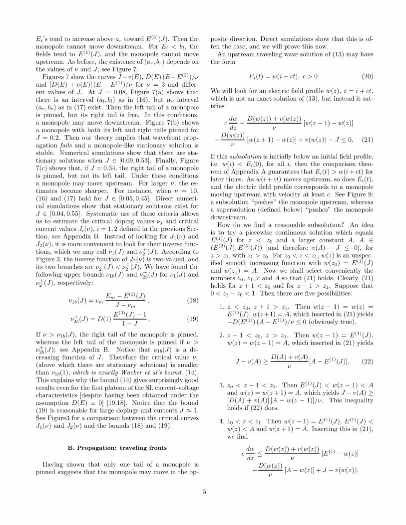
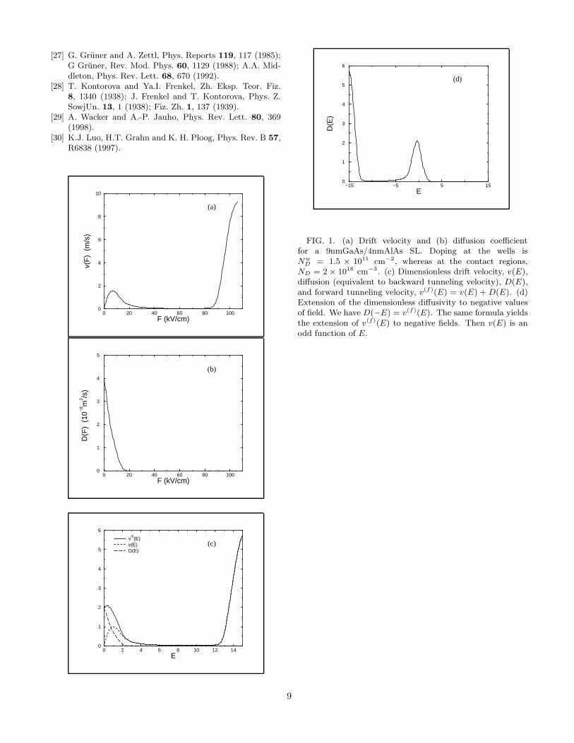
Drift velocity and diffusion coefficient are depicted inFig. 1 for the 9nmGaAs/4nmAlAs SL of Ref. [9]. We haveobtained them from microscopic calculations presented inRef. [18] (which is appropriate for these sample param-eters [29]) by setting v(F ) = J(Nw
D , NwD , F ) (d + w)/Nw
D
and D(F ) = −(∂J(NwD , Nw
D , F )/∂ni+1)(d + w)2. Heree J(ni, ni+1, Fi) is the tunneling current between wells iand i+1, Ji→i+1. We assume that the tunneling currentis a function of the average field at the ith SL period,Fi = F , and of the 2D electron densities at wells i andi + 1, ni and ni+1, respectively. Notice that our modelfor the tunneling current,
eJ(ni, ni+1, Fi) =eniv(Fi)
d + w− eD(Fi)
ni+1 − ni
(d + w)2
≡eniv
(f)(Fi) − eni+1v(b)(Fi)
d + w, (3)
is reasonable for temperatures much lower than a typ-ical Fermi energy in the wells measured from the firstsubband (say 20 meV), [21]. The tunneling current den-sity should change sign if we reverse the electric fieldand exchange the electron densities at wells i and i + 1:J(ni, ni+1, Fi) = −J(ni+1, ni,−Fi). This inversion sym-metry implies
v(f)(−F ) = v(b)(F ) and v(−F ) = −v(F ),
where v(b)(F ) = D(F )/(d + w) and v(f)(F ) = v(F ) +v(b)(F ). See Figure 1(d).
Equations (1) and (2) should be supplemented with ap-propriate bias, initial and boundary conditions. Amongpossible bias conditions, we shall consider the extremecases of current bias (J(t) specified) and voltage bias:
(d + w)N∑
i=1
Fi = V , (4)
with specified V = V (t). Using (4) ignores potentialdrops at the contact regions and at barrier 0, and itoverestimates the contribution of barrier N by a factor1 + w/d [21]. These contributions are negligible for longSL (N = 40 or larger), so that we shall adopt the simplerexpression (4). Appropriate boundary conditions havebeen derived under the same approximations as in (1)[21]. They are
ε
e
dF0
dt+ j(f)
e (F0) −n1w
(b)(F0)
d + w= J(t) , (5)
ε
e
dFN
dt+
nNw(f)(FN )
d + w= J(t) , (6)
where the emitter current density, e j(f)e (F ), the emitter
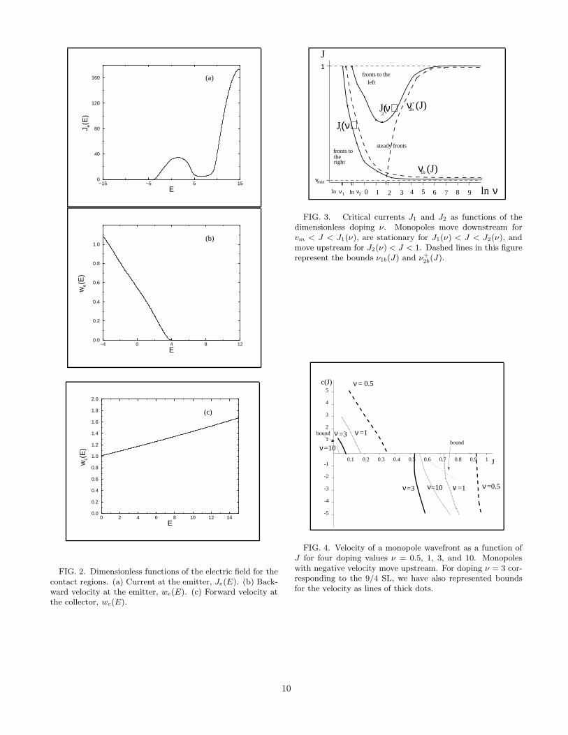
backward velocity, w(b)(F ), and the collector forward ve-locity, w(f)(F ) are functions of the electric field depictedin Fig. 3 of Ref. [21] for contact regions similar to thoseused in experiments [9].
To analyze the discrete drift-diffusion model, it isconvenient to render all equations dimensionless. Letv(F ) reach its first positive maximum at (FM , vM ). Weadopt FM , Nw
D , vM , vM (d + w), eNwDvM/(d + w) and
εFM (d+w)/(eNwDvM ) as the units of Fi, ni, v(F ), D(F ),
eJ and t, respectively. For the first plateau of the 9/4 SLof Ref. [9], we find FM = 6.92 kV/cm, Nw
D = 1.5 × 10¹¹
cm−2, vM = 156 cm/s, vM (d + w) = 2.03 × 10⁻⁴ cm2/sand eNw
DvM/(d+w) = 2.88 A/cm2. The units of currentand time are 0.326 mA and 2.76 ns, respectively. Then(1) to (4) become
dEi
dt+ v(Ei)ni − D(Ei) (ni+1 − ni) = J, (7)
Ei − Ei−1 = ν (ni − 1), (8)
1
N
N∑
i=1
Ei = φ. (9)
2
Here we have used the same symbols for dimensionaland dimensionless quantities except for the electric field(F dimensional, E dimensionless). The parameters ν =eNw
D/(ε FM ) and φ = V/[FMN(d+w)] are dimensionlessdoping and average electric field (bias), respectively. Forthe 9/4 SL, ν ≈ 3. We recall that i = 1, . . . , N − 1 in(7) and i = 1, . . . , N in (8). The boundary conditions (5)and (6) become
dE0
dt+ Je(E0) − we(E0)n1 = J, (10)
dEN
dt+ wc(EN )nN = J, (11)
where
Je(E0) =j(f)e (FM E0) (d + w)
NwDvM
,
we(E0) =w(b)(FM E0)
vM
,
wc(EN ) =w(f)(FM EN )
vM
. (12)
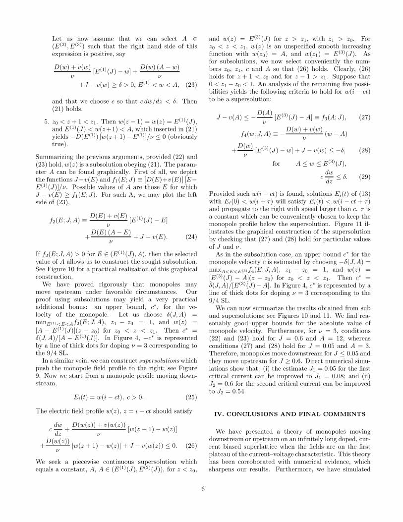
Figure 2 shows Je, we and wc as functions of the elec-tric field. They are dimensionless versions of the curvesplotted in Figure 3 of Ref. [21].
B. Numerical simulations
Simple solutions of the drift-diffusion equations (7) -(8) under constant current bias are stationary or mov-ing monopole wavefronts connecting two electric field do-mains. Let us consider monopole solutions with profiles{Ei} which are increasing functions of i, for they are com-patible with realistic boundary conditions in which theemitter region is highly doped [9]. We have simulatednumerically on a large SL,
dEi
dt−
D(Ei) + v(Ei)
ν(Ei−1 − Ei)
−D(Ei)
ν(Ei+1 − Ei) = J − v(Ei), (13)
with fixed J , which is equivalent to (7) - (8). LetE(1)(J) < E(2)(J) < E(3)(J), be the three solutions ofv(E) = J for vm < J < 1, where (Em, vm) is the min-imum of v(E) for E > 1. For the 9/4 SL of Fig. 1,Em = 9.8571, vm = 0.02192. We have simulated (13)for different values of ν > 0 and of J ∈ (vm, 1). Theinitial condition was chosen so that Ei → E(1)(J) asi → −∞, and Ei → E(3)(J) as i → ∞. We observedthat, after a short transient, a variety of initial condi-tions sharing these features evolved towards either a sta-tionary or moving monopole. For systematic numericalstudies, we therefore adopted an initial step like profile,with Ei = E(1)(J) for i < 0, Ei = E(3)(J) for i > 0
and E0 = E(2)(J). The boundary data were taken to beE−N = E(1)(J), EN = E(3)(J) with N large.
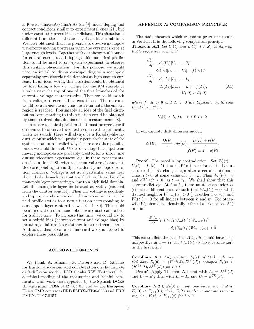
Our results show that the dimensionless doping ν de-termines the type of solution of (13) which is stable.There are two important values of ν, ν1 < ν2.
• For 0 < ν < ν1 and each fixed J ∈ (vm, 1), onlytraveling monopole fronts moving downstream (tothe right) were observed. For ν > ν1, stationarymonopoles were found. According to the argumentsof Wacker et al [19] for the discrete drift modelwith D(E) = 0, stationary monopoles exist for di-mensionless doping larger than a critical value. Anupper bound for this critical doping is
νc = vm
Em − 1
1 − vm
, (14)
which equals νc = 0.198 for our numerical example.We have found that ν1 = 0.16. This agreementwith results obtained assuming D(E) = 0 is notsurprising: we shall prove in Section III that (14)holds as well for the model (7) - (8) with nonzerodiffusivity.
• For ν1 < ν < ν2, traveling fronts moving down-stream exist only if J ∈ (vm, J1(ν)), where J1(ν) <1 is a critical value of the current. If J ∈ (J1(ν), 1),the stable solutions are steady fronts (stationarymonopoles). We have found that ν2 = 0.33.
• New solutions are observed for ν > ν2. As be-fore, there are traveling fronts moving downstreamif J ∈ (vm, J1(ν)), and stationary monopoles ifJ ∈ (J1(ν), J2(ν)), J2(ν) < 1 is a new critical cur-rent. For J2(ν) < J < 1, the stable solutions of (13)are monopoles traveling upstream (to the left). Asν increases, J1(ν) and J2(ν) approach vm and 1,respectively. Thus stationary solutions are foundfor most values of J if ν is large enough.
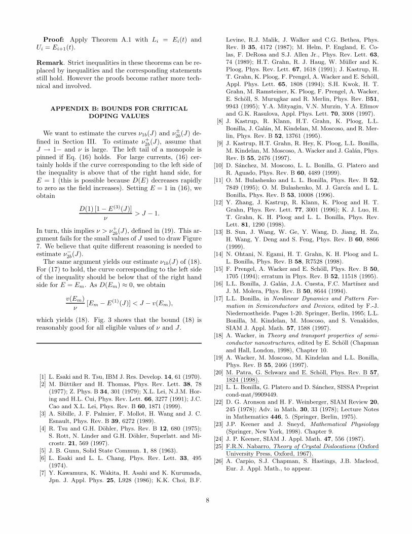
Figure 3 depicts J1(ν) and J2(ν) as functions of ν.Notice that J1 decreases from J1 = 1 to J1 = vm as νincreases from ν1. Similarly, J2 decreases from J2 = 1 toa minimum value J2 ≈ 0.53 and then increases back toJ2 = 1 as ν increases. Monopole velocity as a function ofcurrent has been depicted in Figure 4 for four differentdoping values, ν = 0.5, ν = 1, ν = 3 and ν = 10. Forlarger ν, the interval of J for which stationary solutionsexist becomes wider again, trying to span the whole in-terval (vm, 1) as ν → ∞. For very large ν, the velocitiesof downstream and upstream moving monopoles becomeextremely small in absolute value.
Notice that if we use the complete sequential tunnel-ing current instead of the drift-diffusion approximation(3) in Eq. (1), the situation is the same. Figure 5 de-picts monopole velocity versus current for well dopingcorresponding to the 9/4 SL of Ref. [9]. Results obtainedwith the complete sequential tunneling current or withapproximation (3) (corresponding to Fig. 4 with ν = 3)
3
are compared. Both velocity curves are similar, and theirquantitative discrepancies are irrelevant in view of theuncertainties involved in a theoretical calculation of thetunneling current (typically the off-resonance current islarger than the theoretical prediction).
Once different stable monopole solutions (moving ei-ther downstream or upstream, stationary) have beenidentified, we raise the natural question of whether theyare compatible with boundary conditions. Another seriesof numerical simulations was carried out to answer this.We solved numerically (13) for a current biased finite SL(N = 40) with boundary conditions (10) - (12). Our re-sults are depicted in Figure 6 for realistic doping at thecontact layers. We observe that the emitter boundarycondition results in the creation of a charge accumula-tion layer near this contact. A charge depletion layer isformed near the collector contact as a result of the cor-responding boundary condition. Except for these layers,existence and configuration of monopoles moving down-stream, upstream or remaining stationary, agrees withthe previous simulations (corresponding to an infinitelylong current-biased SL with a monopole-like initial con-dition).
III. MATHEMATICAL ANALYSIS OF
TRAVELING MONOPOLES AND STATIONARY
SOLUTIONS
In this Section, we study theoretically moving or sta-tionary monopoles on an infinitely long, current-biasedSL. Our findings will confirm the picture suggested bythe numerical simulations of the previous Section forany doped weakly coupled SL. Furthermore, we shallprove stability of the different monopole solutions andfind bounds for the critical values of ν and Ji. Ourresults are based upon and extend ideas first proposedby J.P. Keener for discrete FitzHugh-Nagumo equations,corresponding to signal transmision in myelinated neu-rons [24]. Mathematically analogous problems arise inmodels of propagation of defects in crystals [25]. Theseproblems have the following structure,
dEi
dt− d (Ei+1 − 2Ei + Ei−1) = J − v(Ei), (15)
which is much simpler than (13). Here the parameterd > 0 is a constant diffusion coefficient, and v(E) a ‘cu-bic’ function with three branches as the electron driftvelocity of Fig. 1.
For (15), there are critical values of J , J1 and J2,characterizing wavefront behavior [24]. For J > J2(d),there exist wavefront solutions of (15) moving upstream(to the left). For J < J1(d), there are wavefronts mov-ing downstream (to the right), whereas for J1(d) < J <J2(d), stationary fronts exist. The width of the interval(J1(d), J2(d)) is an increasing function of d.
A. Propagation failure and stationary solutions
In Appendix A we state and prove a comparison prin-ciple for (13). As a consequence, if our initial field profileis monopole-like [monotone increasing with well index,and sandwiched between E(1)(J) and E(3)(J)], so is theelectric field profile for any later time t > 0; see AppendixA:
{Ei(0)} increasing with i =⇒
E(1)(J) < Ei(t) < Ei+1(t) < E(3)(J), ∀i, t > 0.
We now obtain sufficient conditions for an initialmonopole not to propagate upstream or downstream.Under these conditions, the monopole may remain sta-tionary or move downstream or upstream, respectively.Let us start with a condition pinning the left tail of amonopole. As Ei−1 < Ei and Ei+1 < E(3)(J), we have:
dEi
dt=
D(Ei)
ν(Ei+1 − Ei)
+D(Ei) + v(Ei)
ν(Ei−1 − Ei) + J − v(Ei)
≤D(Ei)
ν[E(3)(J) − Ei] + J − v(Ei) ≤ 0,
provided there exist al < bl such that
D(E)
ν[E − E(3)(J)] ≥ J − v(E), E ∈ (al, bl), (16)
and then we choose some initial field, Ei(0) ∈ (al, bl).The previous inequality then implies Ei(t) ∈ (E(1)(J), bl)for all t > 0. This in turn forbids a monopole to moveupstream (to the left). We say that condition (16) pinsthe left tail of the monopole. Whether such (al, bl) exist,depends on the parameters ν and J ; see Figure 7.
Let us now pin the right tail of a monopole. AsEi+1 > Ei and Ei−1 > E(1)(J), we have
dEi
dt=
D(Ei)
ν(Ei+1 − Ei)
+D(Ei) + v(Ei)
ν(Ei−1 − Ei) + J − v(Ei)
≥D(Ei) + v(Ei)
ν[E(1)(J) − Ei] + J − v(Ei) ≥ 0,
provided there exist ar < br such that
D(E) + v(E)
ν[E − E(1)(J)] ≤ J − v(E),
E ∈ (ar, br), (17)
and we choose some initial field, Ei(0) ∈ (ar, br). Theprevious inequality then implies Ei(t) ∈ (ar, E
(3)(J)) forall t > 0. A monopole cannot then move downstream (tothe right), and we say that its right tail is pinned. Figure8 illustrates our arguments: for fields larger than ar, the
4
Ei’s tend to increase above ar toward E(3)(J). Then themonopole cannot move downstream. For Ei < bl, thefields tend to E(1)(J), and the monopole cannot moveupstream. As before, the existence of (ar, br) depends onthe values of ν and J ; see Figure 7.
Figures 7 show the curves J−v(E), D(E) (E−E(3))/νand [D(E) + v(E)] (E − E(1))/ν for ν = 3 and differ-ent values of J . At J = 0.08, Figure 7(a) shows thatthere is an interval (al, bl) as in (16), but no interval(ar, br) as in (17) exist. Then the left tail of a monopoleis pinned, but its right tail is free. In this conditions,a monopole may move downstream. Figure 7(b) showsa monopole with both its left and right tails pinned forJ = 0.2. Then our theory implies that wavefront prop-agation fails and a monopole-like stationary solution isstable. Numerical simulations show that there are sta-tionary solutions when J ∈ [0.09, 0.53]. Finally, Figure7(c) shows that, if J = 0.34, the right tail of a monopoleis pinned, but not its left tail. Under these conditionsa monopole may move upstream. For larger ν, the es-timates become sharper. For instance, when ν = 10,(16) and (17) hold for J ∈ [0.05, 0.45]. Direct numeri-cal simulations show that stationary solutions exist forJ ∈ [0.04, 0.55]. Systematic use of these criteria allowsus to estimate the critical doping values νj and criticalcurrent values Ji(ν), i = 1, 2 defined in the previous Sec-tion; see Appendix B. Instead of looking for J1(ν) andJ2(ν), it is more convenient to look for their inverse func-tions, which we may call ν1(J) and ν±
2 (J). According toFigure 3, the inverse function of J2(ν) is two-valued, andits two branches are ν−
2 (J) < ν+2 (J). We have found the
following upper bounds ν1b(J) and ν+2b(J) for ν1(J) and
ν+2 (J), respectively:
ν1b(J) = vm
Em − E(1)(J)
J − vm
, (18)
ν+2b(J) = D(1)
E(3)(J) − 1
1 − J. (19)
If ν > ν1b(J), the right tail of the monopole is pinned,whereas the left tail of the monopole is pinned if ν >ν+2b(J); see Appendix B. Notice that ν1b(J) is a de-
creasing function of J . Therefore the critical value ν1
(above which there are stationary solutions) is smallerthan ν1b(1), which is exactly Wacker et al’s bound, (14).This explains why the bound (14) gives surprisingly goodresults even for the first plateau of the SL current-voltagecharacteristics [despite having been obtained under theassumption D(E) ≡ 0] [19,18]. Notice that the bound(19) is reasonable for large dopings and currents J ≈ 1.See Figure3 for a comparison between the critical curvesJ1(ν) and J2(ν) and the bounds (18) and (19).
B. Propagation: traveling fronts
Having shown that only one tail of a monopole ispinned suggests that the monopole may move in the op-
posite direction. Direct simulations show that this is of-ten the case, and we will prove this now.
An upstream traveling wave solution of (13) may havethe form
Ei(t) = w(i + ct), c > 0. (20)
We will look for an electric field profile w(z), z = i + ct,which is not an exact solution of (13), but instead it sat-isfies
cdw
dz−
D(w(z)) + v(w(z))
ν[w(z − 1) − w(z)]
−D(w(z))
ν[w(z + 1) − w(z)] + v(w(z)) − J ≤ 0. (21)
If this subsolution is initially below an initial field profile,i.e. w(i) < Ei(0), for all i, then the comparison theo-rem of Appendix A guarantees that Ei(t) > w(i + ct) forlater times. As w(i + ct) moves upstream, so does Ei(t),and the electric field profile corresponds to a monopolemoving upstream with velocity at least c. See Figure 9:a subsolution “pushes” the monopole upstream, whereasa supersolution (defined below) “pushes” the monopoledownstream.
How do we find a reasonable subsolution? An ideais to try a piecewise continuous solution which equalsE(1)(J) for z < z0 and a larger constant A, A ∈(E(2)(J), E(3)(J)) [and therefore v(A) − J ≤ 0], forz > z1, with z1 > z0. For z0 < z < z1, w(z) is an unspec-ified smooth increasing function with w(z0) = E(1)(J)and w(z1) = A. Now we shall select conveniently thenumbers z0, z1, c and A so that (21) holds. Clearly, (21)holds for z + 1 < z0 and for z − 1 > z1. Suppose that0 < z1 − z0 < 1. Then there are five possibilities:
1. z < z0, z + 1 > z1. Then w(z − 1) = w(z) =E(1)(J), w(z+1) = A, which inserted in (21) yields−D(E(1)) (A − E(1))/ν ≤ 0 (obviously true).
2. z − 1 < z0, z > z1. Then w(z − 1) = E(1)(J),w(z) = w(z + 1) = A, which inserted in (21) yields
J − v(A) ≥D(A) + v(A)
ν[A − E(1)(J)]. (22)
3. z0 < z − 1 < z1. Then E(1)(J) < w(z − 1) < Aand w(z) = w(z + 1) = A, which yields J − v(A) ≥[D(A) + v(A)] [A − w(z − 1)]/ν. This inequalityholds if (22) does.
4. z0 < z < z1. Then w(z − 1) = E(1)(J), E(1)(J) <w(z) < A and w(z + 1) = A. Inserting this in (21),we find
cdw
dz≤
D(w(z)) + v(w(z))
ν[E(1) − w(z)]
+D(w(z))
ν[A − w(z)] + J − v(w(z)).
5
Let us now assume that we can select A ∈(E(2), E(3)) such that the right hand side of thisexpression is positive, say
D(w) + v(w)
ν[E(1)(J) − w] +
D(w) (A − w)
ν
+J − v(w) ≥ δ > 0, E(1) < w < A, (23)
and that we choose c so that c dw/dz < δ. Then(21) holds.
5. z0 < z + 1 < z1. Then w(z − 1) = w(z) = E(1)(J),and E(1)(J) < w(z+1) < A, which inserted in (21)yields −D(E(1)) [w(z + 1)−E(1)]/ν ≤ 0 (obviouslytrue).
Summarizing the previous arguments, provided (22) and(23) hold, w(z) is a subsolution obeying (21). The param-eter A can be found graphically. First of all, we depictthe functions J−v(E) and f1(E; J) ≡ [D(E)+v(E)] [E−E(1)(J)]/ν. Possible values of A are those E for whichJ − v(E) ≥ f1(E; J). For such A, we may plot the leftside of (23),
f2(E; J, A) ≡D(E) + v(E)
ν[E(1)(J) − E]
+D(E) (A − E)
ν+ J − v(E). (24)
If f2(E; J, A) > 0 for E ∈ (E(1)(J), A), then the selectedvalue of A allows us to construct the sought subsolution.See Figure 10 for a practical realization of this graphicalconstruction.
We have proved rigorously that monopoles maymove upstream under favorable circumstances. Ourproof using subsolutions may yield a very practicaladditional bonus: an upper bound, c∗, for the ve-locity of the monopole. Let us choose δ(J, A) =minE(1)<E<Af2(E; J, A), z1 − z0 = 1, and w(z) =
[A − E(1)(J)](z − z0) for z0 < z < z1. Then c∗ =δ(J, A)/[A − E(1)(J)]. In Figure 4, −c∗ is representedby a line of thick dots for doping ν = 3 corresponding tothe 9/4 SL.
In a similar vein, we can construct supersolutions whichpush the monopole field profile to the right; see Figure9. Now we start from a monopole profile moving down-stream,
Ei(t) = w(i − ct), c > 0. (25)
The electric field profile w(z), z = i − ct should satisfy
cdw
dz+
D(w(z)) + v(w(z))
ν[w(z − 1) − w(z)]
+D(w(z))
ν[w(z + 1) − w(z)] + J − v(w(z)) ≤ 0. (26)
We seek a piecewise continuous supersolution whichequals a constant, A, A ∈ (E(1)(J), E(2)(J)), for z < z0,
and w(z) = E(3)(J) for z > z1, with z1 > z0. Forz0 < z < z1, w(z) is an unspecified smooth increasingfunction with w(z0) = A, and w(z1) = E(3)(J). Asfor subsolutions, we now select conveniently the num-bers z0, z1, c and A so that (26) holds. Clearly, (26)holds for z + 1 < z0 and for z − 1 > z1. Suppose that0 < z1 − z0 < 1. An analysis of the remaining five possi-bilities yields the following criteria to hold for w(i − ct)to be a supersolution:
J − v(A) ≤ −D(A)
ν[E(3)(J) − A] ≡ f3(A; J), (27)
f4(w; J, A) ≡ −D(w) + v(w)
ν(w − A)
+D(w)
ν[E(3)(J) − w] + J − v(w) ≤ −δ, (28)
for A ≤ w ≤ E(3)(J),
cdw
dz≤ δ. (29)
Provided such w(i − ct) is found, solutions Ei(t) of (13)with Ei(0) < w(i + τ) will satisfy Ei(t) < w(i − ct + τ)and propagate to the right with speed larger than c. τ isa constant which can be conveniently chosen to keep themonopole profile below the supersolution. Figure 11 il-lustrates the graphical construction of the supersolutionby checking that (27) and (28) hold for particular valuesof J and ν.
As in the subsolution case, an upper bound c∗ for themonopole velocity c is estimated by choosing −δ(J, A) =maxA<E<E(3)f4(E; J, A), z1 − z0 = 1, and w(z) =
[E(3)(J) − A](z − z0) for z0 < z < z1. Then c∗ =δ(J, A)/[E(3)(J)−A]. In Figure 4, c∗ is represented by aline of thick dots for doping ν = 3 corresponding to the9/4 SL.
We can now summarize the results obtained from suband supersolutions; see Figures 10 and 11. We find rea-sonably good upper bounds for the absolute value ofmonopole velocity. Furthermore, for ν = 3, conditions(22) and (23) hold for J = 0.6 and A = 12, whereasconditions (27) and (28) hold for J = 0.05 and A = 3.Therefore, monopoles move downstream for J ≤ 0.05 andthey move upstream for J ≥ 0.6. Direct numerical simu-lations show that: (i) the estimate J1 = 0.05 for the firstcritical current can be improved to J1 = 0.08; and (ii)J2 = 0.6 for the second critical current can be improvedto J2 = 0.54.
IV. CONCLUSIONS AND FINAL COMMENTS
We have presented a theory of monopoles movingdownstream or upstream on an infinitely long doped, cur-rent biased superlattice when the fields are on the firstplateau of the current–voltage characteristic. This theoryhas been corroborated with numerical evidence, whichsharpens our results. Furthermore, we have simulated
6
a 40-well 9nmGaAs/4nmAlAs SL [9] under doping andcontact conditions similar to experimental ones [21], butunder constant current bias conditions. This situation isdifferent from the usual case of voltage bias conditions.We have obtained that it is possible to observe monopolewavefronts moving upstream when the current is kept atlarge enough levels. Together with our theoretical boundsfor critical currents and dopings, this numerical predic-tion could be used to set up an experiment to observethis striking phenomenon. For this purpose, we wouldneed an initial condition corresponding to a monopoleseparating two electric field domains at high enough cur-rent. In an ideal world, this situation could be obtainedby first fixing a low dc voltage for the 9/4 sample ata value near the top of one of the first branches of thecurrent - voltage characteristics. Then we could switchfrom voltage to current bias conditions. The outcomewould be a monopole moving upstream until the emitterregion is reached. Presumably an idea of the field distri-bution corresponding to this situation could be obtainedby time-resolved photoluminescence measurements [8].
There are technical problems that must be overcome ifone wants to observe these features in real experiments:when we switch, there will always be a Faraday-like in-ductive pulse which will probably perturb the state of thesystem in an uncontrolled way. There are other possiblebiases we could think of. Under dc voltage bias, upstreammoving monopoles are probably created for a short timeduring relocation experiment [30]. In these experiments,one has a doped SL with a current-voltage characteris-tics correponding to multiple stationary monopole solu-tion branches. Voltage is set at a particular value nearthe end of a branch, so that the field profile is that of amonopole layer connecting a low to a high field domain.Let the monopole layer be located at well i (countedfrom the emitter contact). Then the voltage is suddenlyand appropriately increased. After a certain time, thefield profile settles to a new situation corresponding toa monopole layer centered at well i − 1 [30]. This couldbe an indication of a monopole moving upstream, albeitfor a short time. To increase this time, we could try toset a hybrid bias (between current and voltage bias) byincluding a finite series resistance in our external circuit.Additional theoretical and numerical work is needed toexplore these possibilities.
ACKNOWLEDGMENTS
We thank A. Amann, G. Platero and D. Sanchezfor fruitful discussions and collaboration on the discretedrift-diffusion model. LLB thanks S.W. Teitsworth fora critical reading of the manuscript and helpful com-ments. This work was supported by the Spanish DGESthrough grant PB98-0142-C04-01, and by the EuropeanUnion TMR contracts ERB FMRX-CT96-0033 and ERBFMRX-CT97-0157.
APPENDIX A: COMPARISON PRINCIPLE
The main theorem which we use to prove our resultsin Section III is the following comparison principle:Theorem A.1 Let Ui(t) and Li(t), i ∈ Z, be differen-tiable sequences such that
dUi
dt− d1(Ui)[Ui+1 − Ui]
−d2(Ui)[Ui−1 − Ui] − f(Ui) ≥
dLi
dt− d1(Li)[Li+1 − Li]
−d2(Li)[Li−1 − Li] − f(Li), (A1)
Ui(0) > Li(0).
where f , d1 > 0 and d2 > 0 are Lipschitz continuousfunctions. Then,
Ui(t) > Li(t), t > 0, i ∈ Z
In our discrete drift-diffusion model,
d1(E) =D(E)
ν, d2(E) =
D(E) + v(E)
ν,
f(E) = J − v(E).
Proof: The proof is by contradiction. Set Wi(t) =Ui(t) − Li(t). At t = 0, Wi(0) > 0 for all i. Let usassume that Wi changes sign after a certain minimumtime t1 > 0, at some value of i, i = k. Thus Wk(t1) = 0and dWk/dt ≤ 0, as t → t1. We shall show that thisis contradictory. At t = t1, there must be an index m(equal or different from k) such that Wm(t1) = 0, whileits next neighbor Wm+j(t1) > 0 (j is either 1 or -1), andWi(t1) = 0 for all indices between k and m. For other-wise Wk should be identically 0 for all k. Equation (A1)implies
dWm
dt(t1) ≥ d1(Um(t1))Wm+1(t1)
+d2(Um(t1))Wm−1(t1) > 0.
This contradicts the fact that dWm/dt should have beennonpositive as t → t1, for Wm(t1) to have become zeroin the first place.
Corollary A.1 Any solution Ei(t) of (13) with ini-tial data Ei(0) ∈ (E(1)(J), E(3)(J)) satisfies Ei(t) ∈(E(1)(J), E(3)(J)) for t > 0.
Proof: Apply Theorem A.1 first with Li = E(1)(J)and Ui = Ei, then with Li = Ei and Ui = E(3)(J).
Corollary A.2 If Ei(0) is monotone increasing, that is,Ei(0) < Ei+1(0), then, Ei(t) is also monotone increas-ing, i.e., Ei(t) < Ei+1(t) for t > 0.
7
Proof: Apply Theorem A.1 with Li = Ei(t) andUi = Ei+1(t).
Remark. Strict inequalities in these theorems can be re-placed by inequalities and the corresponding statementsstill hold. However the proofs become rather more tech-nical and involved.
APPENDIX B: BOUNDS FOR CRITICAL
DOPING VALUES
We want to estimate the curves ν1b(J) and ν±
2b(J) de-
fined in Section III. To estimate ν+2b(J), assume that
J → 1− and ν is large. The left tail of a monopole ispinned if Eq. (16) holds. For large currents, (16) cer-tainly holds if the curve corresponding to the left side ofthe inequality is above that of the right hand side, forE = 1 (this is possible because D(E) decreases rapidlyto zero as the field increases). Setting E = 1 in (16), weobtain
D(1) [1 − E(3)(J)]
ν> J − 1.
In turn, this implies ν > ν+2b(J), defined in (19). This ar-
gument fails for the small values of J used to draw Figure7. We believe that quite different reasoning is needed toestimate ν−
2b(J).The same argument yields our estimate ν1b(J) of (18).
For (17) to hold, the curve corresponding to the left sideof the inequality should be below that of the right handside for E = Em. As D(Em) ≈ 0, we obtain
v(Em)
ν[Em − E(1)(J)] < J − v(Em),
which yields (18). Fig. 3 shows that the bound (18) isreasonably good for all eligible values of ν and J .
[1] L. Esaki and R. Tsu, IBM J. Res. Develop. 14, 61 (1970).[2] M. Buttiker and H. Thomas, Phys. Rev. Lett. 38, 78
(1977); Z. Phys. B 34, 301 (1979); X.L. Lei, N.J.M. Hor-ing and H.L. Cui, Phys. Rev. Lett. 66, 3277 (1991); J.C.Cao and X.L. Lei, Phys. Rev. B 60, 1871 (1999).
[3] A. Sibille, J. F. Palmier, F. Mollot, H. Wang and J. C.Esnault, Phys. Rev. B 39, 6272 (1989).
[4] R. Tsu and G.H. Dohler, Phys. Rev. B 12, 680 (1975);S. Rott, N. Linder and G.H. Dohler, Superlatt. and Mi-crostr. 21, 569 (1997).
[5] J. B. Gunn, Solid State Commun. 1, 88 (1963).[6] L. Esaki and L. L. Chang, Phys. Rev. Lett. 33, 495
(1974).[7] Y. Kawamura, K. Wakita, H. Asahi and K. Kurumada,
Jpn. J. Appl. Phys. 25, L928 (1986); K.K. Choi, B.F.
Levine, R.J. Malik, J. Walker and C.G. Bethea, Phys.Rev. B 35, 4172 (1987); M. Helm, P. England, E. Co-las, F. DeRosa and S.J. Allen Jr., Phys. Rev. Lett. 63,74 (1989); H.T. Grahn, R. J. Haug, W. Muller and K.Ploog, Phys. Rev. Lett. 67, 1618 (1991); J. Kastrup, H.T. Grahn, K. Ploog, F. Prengel, A. Wacker and E. Scholl,Appl. Phys. Lett. 65, 1808 (1994); S.H. Kwok, H. T.Grahn, M. Ramsteiner, K. Ploog, F. Prengel, A. Wacker,E. Scholl, S. Murugkar and R. Merlin, Phys. Rev. B51,9943 (1995); Y.A. Mityagin, V.N. Murzin, Y.A. Efimovand G.K. Rasulova, Appl. Phys. Lett. 70, 3008 (1997).
[8] J. Kastrup, R. Klann, H.T. Grahn, K. Ploog, L.L.Bonilla, J. Galan, M. Kindelan, M. Moscoso, and R. Mer-lin, Phys. Rev. B 52, 13761 (1995).
[9] J. Kastrup, H.T. Grahn, R. Hey, K. Ploog, L.L. Bonilla,M. Kindelan, M. Moscoso, A. Wacker and J. Galan, Phys.Rev. B 55, 2476 (1997).
[10] D. Sanchez, M. Moscoso, L. L. Bonilla, G. Platero andR. Aguado, Phys. Rev. B 60, 4489 (1999).
[11] O. M. Bulashenko and L. L. Bonilla, Phys. Rev. B 52,7849 (1995); O. M. Bulashenko, M. J. Garcıa and L. L.Bonilla, Phys. Rev. B 53, 10008 (1996).
[12] Y. Zhang, J. Kastrup, R. Klann, K. Ploog and H. T.Grahn, Phys. Rev. Lett. 77, 3001 (1996); K. J. Luo, H.T. Grahn, K. H. Ploog and L. L. Bonilla, Phys. Rev.Lett. 81, 1290 (1998).
[13] B. Sun, J. Wang, W. Ge, Y. Wang, D. Jiang, H. Zu,H. Wang, Y. Deng and S. Feng, Phys. Rev. B 60, 8866(1999).
[14] N. Ohtani, N. Egami, H. T. Grahn, K. H. Ploog and L.L. Bonilla, Phys. Rev. B 58, R7528 (1998).
[15] F. Prengel, A. Wacker and E. Scholl, Phys. Rev. B 50,1705 (1994); erratum in Phys. Rev. B 52, 11518 (1995).
[16] L.L. Bonilla, J. Galan, J.A. Cuesta, F.C. Martınez andJ. M. Molera, Phys. Rev. B 50, 8644 (1994).
[17] L.L. Bonilla, in Nonlinear Dynamics and Pattern For-
mation in Semiconductors and Devices, edited by F.-J.Niedernostheide. Pages 1-20. Springer, Berlin, 1995; L.L.Bonilla, M. Kindelan, M. Moscoso, and S. Venakides,SIAM J. Appl. Math. 57, 1588 (1997).
[18] A. Wacker, in Theory and transport properties of semi-
conductor nanostructures, edited by E. Scholl (Chapmanand Hall, London, 1998), Chapter 10.
[19] A. Wacker, M. Moscoso, M. Kindelan and L.L. Bonilla,Phys. Rev. B 55, 2466 (1997).
[20] M. Patra, G. Schwarz and E. Scholl, Phys. Rev. B 57,1824 (1998).
[21] L. L. Bonilla, G. Platero and D. Sanchez, SISSA Preprintcond-mat/9909449.
[22] D. G. Aronson and H. F. Weinberger, SIAM Review 20,245 (1978); Adv. in Math. 30, 33 (1978); Lecture Notesin Mathematics 446, 5. (Springer, Berlin, 1975).
[23] J.P. Keener and J. Sneyd, Mathematical Physiology
(Springer, New York, 1998). Chapter 9.[24] J. P. Keener, SIAM J. Appl. Math. 47, 556 (1987).[25] F.R.N. Nabarro, Theory of Crystal Dislocations (Oxford
University Press, Oxford, 1967).[26] A. Carpio, S.J. Chapman, S. Hastings, J.B. Macleod,
Eur. J. Appl. Math., to appear.
8
[27] G. Gruner and A. Zettl, Phys. Reports 119, 117 (1985);G Gruner, Rev. Mod. Phys. 60, 1129 (1988); A.A. Mid-dleton, Phys. Rev. Lett. 68, 670 (1992).
[28] T. Kontorova and Ya.I. Frenkel, Zh. Eksp. Teor. Fiz.8, 1340 (1938); J. Frenkel and T. Kontorova, Phys. Z.SowjUn. 13, 1 (1938); Fiz. Zh. 1, 137 (1939).
[29] A. Wacker and A.-P. Jauho, Phys. Rev. Lett. 80, 369(1998).
[30] K.J. Luo, H.T. Grahn and K. H. Ploog, Phys. Rev. B 57,R6838 (1997).
0 20 40 60 80 100F (kV/cm)
0
2
4
6
8
10
v(F
) (
m/s
)
(a)
0 20 40 60 80 100F (kV/cm)
0
1
2
3
4
5
D(F
) (
10−
8 m2 /s
)
(b)
0 2 4 6 8 10 12 14E
0
1
2
3
4
5
6
v(f)
(E)v(E)D(E)
(c)
−15 −5 5 15E
0
1
2
3
4
5
6
D(E
)
(d)
FIG. 1. (a) Drift velocity and (b) diffusion coefficientfor a 9nmGaAs/4nmAlAs SL. Doping at the wells isNw
D = 1.5 × 1011 cm−2, whereas at the contact regions,ND = 2 × 1018 cm−3. (c) Dimensionless drift velocity, v(E),diffusion (equivalent to backward tunneling velocity), D(E),and forward tunneling velocity, v(f)(E) = v(E) + D(E). (d)Extension of the dimensionless diffusivity to negative valuesof field. We have D(−E) = v(f)(E). The same formula yieldsthe extension of v(f)(E) to negative fields. Then v(E) is anodd function of E.
9
−15 −5 5 15E
0
40
80
120
160
J e(E
)(a)
−4 0 4 8 12E
0.0
0.2
0.4
0.6
0.8
1.0
we(
E)
(b)
0 2 4 6 8 10 12 14E
0.0
0.2
0.4
0.6
0.8
1.0
1.2
1.4
1.6
1.8
2.0
wc(
E)
(c)
FIG. 2. Dimensionless functions of the electric field for thecontact regions. (a) Current at the emitter, Je(E). (b) Back-ward velocity at the emitter, we(E). (c) Forward velocity atthe collector, wc(E).
1
vmin
0νν1 2
fronts totheright
fronts to theleft
steady fronts
1 2 3 987654
J
ln ν ln ln
J1(ν)
2b
1b
2ν)
ν
ν J( (J) +
(J)
FIG. 3. Critical currents J1 and J2 as functions of thedimensionless doping ν. Monopoles move downstream forvm < J < J1(ν), are stationary for J1(ν) < J < J2(ν), andmove upstream for J2(ν) < J < 1. Dashed lines in this figurerepresent the bounds ν1b(J) and ν+
2b(J).
ν
c(J)
=3 =0.5
J
ν
ν νbound
0.1 0.2 0.3 0.4 0.5 0.6 0.7 0.8 0.9 1
5
4
3
2
1
-1
-2
-3
-4
-5
= 0.5
=1 =3
=10ν
bound
ν =1νν=10 ν
FIG. 4. Velocity of a monopole wavefront as a function ofJ for four doping values ν = 0.5, 1, 3, and 10. Monopoleswith negative velocity move upstream. For doping ν = 3 cor-responding to the 9/4 SL, we have also represented boundsfor the velocity as lines of thick dots.
10

FIG. 5. Monopole velocity as a function of current for the9/4 SL. Comparison of results for the discrete drift-diffusionmodel (1) - (2) with ν = 3 (thick line), and those obtained byusing the exact tunneling current eJ(ni, ni+1, Fi) (thin line)instead of approximation (3).
-5
0
5
10
15
0 5 10 15 20 25 30 35 40
Ele
ctric
Fie
ld E
Well
(a)
-5
0
5
10
15
0 5 10 15 20 25 30 35 40
Ele
ctric
Fie
ld E
Well
(b)
-5
0
5
10
15
0 5 10 15 20 25 30 35 40
Ele
ctric
Fie
ld E
Well
(c)
FIG. 6. Numerical simulations of the drift-diffusion modelwith realistic boundary conditions at the contact regions. (a)Monopole moving downstream for J = 0.023, (b) stationarymonopole for J = 0.3, and (c) monopole moving upstream forJ = 0.9. In all cases, diamonds correspond to the profile att = 0 and squares to the profile at the largest positive time.
-1
-0.8
-0.6
-0.4
-0.2
0
0.2
0.4
0.6
0 2 4 6 8 10 12 14E
(a)
-1
-0.8
-0.6
-0.4
-0.2
0
0.2
0.4
0.6
0 2 4 6 8 10 12 14E
(b)
11
-0.6
-0.4
-0.2
0
0.2
0.4
0.6
0 2 4 6 8 10 12 14E
(c)
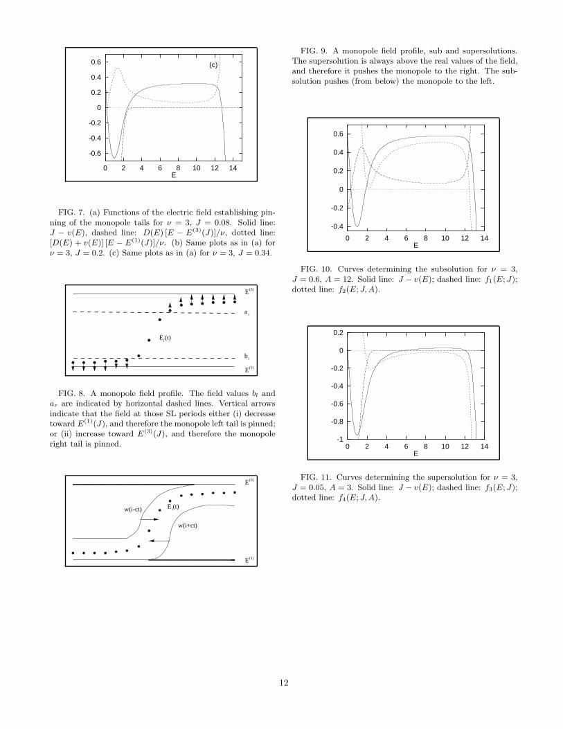
FIG. 7. (a) Functions of the electric field establishing pin-ning of the monopole tails for ν = 3, J = 0.08. Solid line:J − v(E), dashed line: D(E) [E − E(3)(J)]/ν, dotted line:[D(E) + v(E)] [E − E(1)(J)]/ν. (b) Same plots as in (a) forν = 3, J = 0.2. (c) Same plots as in (a) for ν = 3, J = 0.34.
E
b
a
l
r
E (t)i
E(1)
(3)
FIG. 8. A monopole field profile. The field values bl andar are indicated by horizontal dashed lines. Vertical arrowsindicate that the field at those SL periods either (i) decreasetoward E(1)(J), and therefore the monopole left tail is pinned;or (ii) increase toward E(3)(J), and therefore the monopoleright tail is pinned.
E
E
w(i-ct)
w(i+ct)
E (t)i
(3)
(1)
FIG. 9. A monopole field profile, sub and supersolutions.The supersolution is always above the real values of the field,and therefore it pushes the monopole to the right. The sub-solution pushes (from below) the monopole to the left.
-0.4
-0.2
0
0.2
0.4
0.6
0 2 4 6 8 10 12 14E
FIG. 10. Curves determining the subsolution for ν = 3,J = 0.6, A = 12. Solid line: J − v(E); dashed line: f1(E;J);dotted line: f2(E; J, A).
-1
-0.8
-0.6
-0.4
-0.2
0
0.2
0 2 4 6 8 10 12 14E
FIG. 11. Curves determining the supersolution for ν = 3,J = 0.05, A = 3. Solid line: J − v(E); dashed line: f3(E;J);dotted line: f4(E; J, A).
12


![Magnetorefractive and Kerr effects in the [La0.67Ca0.33MnO3/La0.67Sr0.33MnO3]n superlattices](https://img.pdfslide.net/doc/110x75/6354f7048ae64d6d7f0aebd7/magnetorefractive-and-kerr-effects-in-the-la067ca033mno3la067sr033mno3n-superlattices.jpg)


