Embed Size (px)
Citation preview

p s sapplications and materials science
a
statu
s
soli
di
www.pss-a.comph
ysi
ca
REPRINT
Waveguiding, absorption and emission properties
of dye-impregnated oxidized porous silicon
D. Navarro-Urrios1, 2
, M. Ghulinyan1
, N. E. Capuj2
, C. J. Oton2
, F. Riboli1
,
I. R. Martín3
, and L. Pavesi1
1
Nanoscience Laboratory, Department of Physics, University of Trento, Italy
2
Dpto. de Física Básica, University of La Laguna, Tenerife, Spain
3
Dpto. de Física Fund. y Exp. Electr. y Sist., University of La Laguna, Tenerife, Spain
Received 17 March 2006, revised 14 December 2006, accepted 18 December 2006
Published online 2 May 2007
PACS 42.79.Gn, 78.30.Am, 78.30.Ly, 78.55.Mb
The waveguiding, absorption and emission properties of oxidised porous silicon waveguides when
impregnated with Nile Blue have been studied. We present m-line measurements before and after the im-
pregnation showing that the effective indices of the modes remain the same. When performing guided lu-
minescence experiments, a structured emission band is measured. Using the refractive index profile
extracted from m-line measurements it has been possible to simulate the emission lineshape assuming the
observation of an interference pattern formed across the waveguide. We demonstrate that these oscilla-
tions appear because in the first hundreds of nanometers the dye concentration is several orders of magni-
tude higher than in the rest of the sample.
phys. stat. sol. (a) 204, No. 5, 1502–1506 (2007) / DOI 10.1002/pssa.200674403

phys. stat. sol. (a) 204, No. 5, 1502–1506 (2007) / DOI 10.1002/pssa.200674403
© 2007 WILEY-VCH Verlag GmbH & Co. KGaA, Weinheim
Waveguiding, absorption and emission properties
of dye-impregnated oxidized porous silicon
D. Navarro-Urrios*, 1, 2, M. Ghulinyan1, N. E. Capuj2, C. J. Oton**, 2, F. Riboli1,
I. R. Martín3, and L. Pavesi1
1 Nanoscience Laboratory, Department of Physics, University of Trento, Italy
2 Dpto. de Física Básica, University of La Laguna, Tenerife, Spain
3 Dpto. de Física Fund. y Exp. Electr. y Sist., University of La Laguna, Tenerife, Spain
Received 17 March 2006, revised 14 December 2006, accepted 18 December 2006
Published online 2 May 2007
PACS 42.79.Gn, 78.30.Am, 78.30.Ly, 78.55.Mb
The waveguiding, absorption and emission properties of oxidised porous silicon waveguides when
impregnated with Nile Blue have been studied. We present m-line measurements before and after the im-
pregnation showing that the effective indices of the modes remain the same. When performing guided lu-
minescence experiments, a structured emission band is measured. Using the refractive index profile
extracted from m-line measurements it has been possible to simulate the emission lineshape assuming the
observation of an interference pattern formed across the waveguide. We demonstrate that these oscilla-
tions appear because in the first hundreds of nanometers the dye concentration is several orders of magni-
tude higher than in the rest of the sample.
© 2007 WILEY-VCH Verlag GmbH & Co. KGaA, Weinheim
1 Introduction
The recent observation of positive optical gain measured under pulsed excitation in oxidized porous
silicon planar waveguides impregnated with a dye [1] has led us to make a deeper study on the
waveguide properties, absorption and emission properties of the impregnated samples. Moreover, guided
luminescence experiments in active waveguides where Silicon nanocrystals are contained in the core,
showed a structured emission due to their modal structure [2, 3]. We were thus motivated to look for
similar effects in porous silicon active waveguides.
2 Experiment
Porous silicon samples were fabricated by electrochemical etching of heavily doped (0.01 Ω cm resistiv-
ity) p-type silicon. The electrolyte was made by mixing 31% of aqueous HF (48 wt%) with ethanol. Two
layers were grown (a core and a cladding layer) by applying current densities of 40 and 80 mA/cm2,
respectively, to a 1 cm2 circular area. The samples were then annealed at 900 °C for 3 hours in order to
completely oxidize the structure, making it porous silica. The passive waveguide properties of this
waveguide type have been already described in Ref. [4]. To render the waveguide optically active, the
samples were immersed in different concentrations (10–6–10–4 M) of an ethanoic solution of Nile Blue
(LC 6900) [5], and then dried in air to let evaporate the solvent.
* Corresponding author: e-mail: [email protected], Phone: +39 0461882030, Fax: +39 0461881696 ** Present address: Optoelectronics Research Centre, University of Southampton, UK

phys. stat. sol. (a) 204, No. 5 (2007) 1503
www.pss-a.com © 2007 WILEY-VCH Verlag GmbH & Co. KGaA, Weinheim
Original
Paper
1.15 1.20 1.25 1.30 1.35
1
2
3
4
5
TM before imp.TM after imp.
TE before imp.TE after imp.
Inte
nsity
(a.u
.)
effective index
To characterize the optical properties of the waveguides, standard m-line measurements have been
performed with the 633 nm line of a He–Ne laser. From this kind of measurements, it is possible to
extract the refractive material index of the core and cladding layer and the thickness of the core layer.
Photoluminescence (PL) measurements were performed by using the 514.5 nm line of a CW Ar laser
focusing it into a 10 µm wide and 1.2 mm long stripe. The pump power density was always kept well
below the stimulated emission threshold [1]. The emitted light was collected with an optical fiber
(N.A. = 0.025) and analysed by a monochromator and a CCD.
3 Results
In order to evaluate the effect of the presence of the dye on the waveguiding properties of the samples we
performed m-line measurements before and after the dye infiltration and the solvent evaporation. In
Fig. 1 the m-line measurements for a multimode waveguide are reported. A series of dips is observed
which corresponds to the effective refractive indices of the various optical modes of the waveguide.
The modal structure and the effective refractive indices are not changed by the dye infiltration. The only
550 600 650 700 750
0
500
1000
1500
2000
2500
Inte
nsity
(a.u
)
Wavelength (nm)
Guided PLAir TEAir TM
b)
0.0
0.4
0.8
1.2Absorption
Surface PLa)
screen
collecting optical fiber
position B
position A waveguide
Fig. 2 Left: a) Absorption of Nile Blue (from [5]) and surface luminescence from the waveguide. b) Guided PL
spectrum (solid black, fiber position A) and TE (dashed line, fiber position B) and TM (dotted line, fiber position B)
non guided PL signal propagating in air and parallel to the sample surface. Note that in panel b) the intensity scale is
the same for all spectra. Right: scheme of the experiments. The collecting optical fiber is placed in position A for the
measurements of the guided PL, while it is placed in position B when the non guided PL is measured (refer as Air
TE or Air TM in Fig. 2b left). When a screen is placed as indicated the non guided PL vanishes.
Fig. 1 m-line characterization of a multimode wave-
guide at 633 nm, before (black line) and after (grey line)
dye infiltration where the starting dye solution was
10–4 M. TE and TM refer to the two polarizations.
1504 D. Navarro-Urrios et al.: Waveguiding, absorption and emission properties
© 2007 WILEY-VCH Verlag GmbH & Co. KGaA, Weinheim www.pss-a.com
effect observed is a broadening of the dips which is usually attributed to an increase of the waveguide ab-
sorption. This is a confirmation of the Nile-Blue infiltration since Nile-Blue molecules absorb at the used
wavelength. Indeed if the pumping is high enough, above threshold for population inversion, Nile-Blue
molecules eventually show gain [1]. A fit to the m-line results allow to get the material refractive index that
for the waveguide shown in Fig. 1 results in a material index of 1.36 and a core layer thickness of 2.4 µm.
The presence of the infiltrated dye is also witnessed by the emission which is observed when the
waveguide is photoexcited. In Fig. 2 left, we report both the surface emission (top panel) and the
waveguide facet emission which is due to the light emitted by the dye molecules and which is guided by
the waveguide (bottom panel). The guided emission is essentially the product of the surface emission
times the waveguide losses due to the dye absorption. A particular feature is observed when the collect-
ing fiber is slightly misplaced from the waveguide optical axis (Fig. 2 right): polarization dependent
oscillations modulate the emission spectrum (dashed and dotted lines in the bottom panel of Fig. 2 left).
This signal is due to non-guided light which travels in the air parallel to the surface of the sample. In fact
when a screen is placed perpendicular to the waveguide surface at the waveguide end (Fig. 2 right) the
oscillations disappeared. This demonstrates that these oscillations are due to a different phenomenon than
the waveguide filtering effect due to the modal structure of the waveguide recently reported by Khriacht-
chev et al. [2] and Valenta et al. [3]. In addition their presence raises a note of caution when collecting
guided light from such waveguides due to possible misalignments which can lead to erroneous results.
0 2 4 6 8 10 12 14
1.0
1.1
1.2
1.3
n mat
thickness (µm)
no
ne
0.20.40.60.81.0
TM expTM simN
orm
alis
edin
tens
ity
1.10 1.15 1.20 1.25
0.20.40.60.81.0
TEexpTE sim
neff a)
600 650 700 750 800
0.0
0.2
0.4
0.6
0.8
1.0
ExperimentalSimulation (first 300nm )
Wavelength (nm)
Nor
mal
ised
Inte
nsity
0.0
0.2
0.4
0.6
0.8
1.0
b)
ExperimentalSimulation (whole structure)
Fig. 4 a) m-line measurements (black) and simulations (grey) of the waveguide of Fig. 2 for TE (top panel) and
TM (middle panel) polarizations. The bottom panel shows the ordinary (black, no) and extraordinary (grey, ne) re-
fractive index profile extracted from the simulations. A thickness of 2.7 µm for the core and of 11 µm for the clad-
ding layer has been also deduced. b) TE non guided PL measurements (black) and simulations (grey). The simula-
tion in the top panel assumes that emitters are distributed along the whole core and cladding thicknesses while they
occupy only the first 300 nm for the simulation reported in the bottom panel.
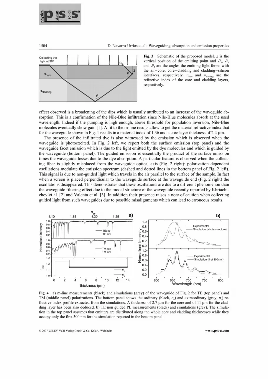
Fig. 3 Schematic of the proposed model. z is the
vertical position of the emitting point and ϑ 0, ϑ 1
and ϑ 2 are the angles the emitting light forms with
the air–core, core–cladding and cladding–silicon
interfaces, respectively. ncore and ncladding are the
refractive index of the core and cladding layers,
respectively.

phys. stat. sol. (a) 204, No. 5 (2007) 1505
www.pss-a.com © 2007 WILEY-VCH Verlag GmbH & Co. KGaA, Weinheim
Original
Paper
600 640 680 720 760 800
0.0
0.2
0.4
0.6
0.8
1.0ExperimentalSimulation (first 300nm)
Nor
mal
ised
Inte
nsity
Wavelength (nm)
Note that the non-guided emissions have peculiar polarization dependent characteristics with anti-
phase oscillation in TE and TM. In Fig. 2 left, the TM spectrum (dotted line) is weaker than the TE
spectrum (dashed line) since the polarization of the pumping light is parallel to TE and is more efficient
exciting the TE than the TM. Finally, no change in the non-guided PL lineshape was observed when
exciting only a spot on the waveguide surface or the whole waveguide length. The explanation of the
oscillations in the non-guided PL resides in an interference effect caused by reflection of light at the
cladding-silicon interface (Fig. 3). A model can be developed by considering a set of incoherent emitters
distributed in the core layer, where only the light emitted by a single emitter can interfere with itself.
Thus, we model a linear distribution of emitters along the waveguide thickness and calculate the interfer-
ence pattern of the light which is collected parallel to the waveguide surface: the signal observed from a
single emitter is the result of the interference between the two rays emitted and travelling upwards and
downwards, respectively, that leave the waveguide at the angle of observation (Fig. 3). The spectral
distribution of the emission intensity for the single emitters is taken equal to the surface emission spec-
trum. From now on the discussion will be centred in the TE signal although the results and conclusions
are consistent for both polarizations. It should also be noted that the samples show positive birefringence
[6], i.e. for TM the extraordinary mode propagates with a refractive index that depends on the angle.
The ordinary and extraordinary refractive index profile of the core and cladding layers, as well as,
their thicknesses are extracted from a fit of the m-line measurements. In Fig. 4a we show the m-line
measurements, simulations and the extracted refractive index profiles of the waveguide whose emission
data are shown in Fig. 2. From these data, the optical path of emitted rays can be calculated within our
model. In Fig. 4b we report the results. We have first assumed that emitters are distributed in the whole
waveguide (core and cladding layers) and that all the emitters have the same emission intensity. The
result resembles the surface PL (grey curve of top panel in Fig. 4b): no oscillations are observed. To find
oscillations in the simulated spectra we have to assume that the emitters are concentrated in a region
300 nm thick under the waveguide surface. With this hypothesis the non-guided PL is reproduced quite
well (Fig. 4b bottom panel).
Another example is shown in Fig. 5. Here a waveguide with the same core but a thicker cladding layer
is used. Comparing Fig. 5 with Fig. 4b, we observe that, the larger cladding thickness is reflected in more
finely spaced oscillations due to the longer optical path and that the contrast in the oscillations is smaller
because the larger cladding thickness implies a smaller incidence angle on the cladding-silicon interface
and, hence, a smaller reflectivity of the interface. Again the simulation is able to reproduce the lineshape
only when the emitters are concentrated in the first 300 nm.
Thus the simulations indicate that either only the first 300 nm layer are effectively pumped by the
laser beam or that the dye molecules infiltrate only this thickness. The first hypothesis entails that the
losses at the pumping wavelength should be of the order of 104–105 cm–1, values much higher than what
can be expected from the absorption of the dye. Moreover, although the PL intensity is almost linearly
Fig. 5 TE non guided PL measurement (black) and simu-
lation (grey). Simulation assumes only the first 300 nm
occupied by emitters. The waveguide thicknesses are
2.8 µm and 30 µm for the core and cladding layers.

1506 D. Navarro-Urrios et al.: Waveguiding, absorption and emission properties
© 2007 WILEY-VCH Verlag GmbH & Co. KGaA, Weinheim www.pss-a.com
dependent on the concentration of the dye solution and on the pumping wavelength, any remarkable
change in the contrast of the interferences is observed by their variations. Thus, we are left with the fact
that the concentration of dye decreases by orders of magnitude along the waveguide after the first
300 nm due to the limited infiltration into the oxidized porous silicon. The reduced region of high quality
infiltration does not affect to the observation of optical gain on compact planar waveguides [1], as the
core thickness in this case is also around 300 nm. In any case, the quality of the infiltration can be im-
proved by increasing the porosity of the top layer, although this reduces the refractive index contrast
between core and cladding.
4 Conclusions
In this work it has been reported the presence of oscillations in the non-guided PL spectra of dye infil-
trated high quality oxidized porous silicon waveguides. These observations have been modelled by an
interference effects in the emission of a set of incoherent emitters distributed only in a thin layer under
the waveguide surface due to the limited in-diffusion of the dye solution. The good agreement between
simulation and experimental data is strongly dependent on the careful determination of the waveguide
parameters which is only possible by a fit of the full m-line measurements.
Acknowledgement We acknowledge Leonid Khriachtchev for fruitful discussions. This work has been carried out
with the financial support of Comisión Interministerial de Ciencia y Tecnología (MAT 2004-6868), Gobierno
Autónomo de Canarias (PI042004/018), and MIUR (RBNE01P4JF and RBNE012N3X).
References
[1] C. J. Oton, D. Navarro-Urrios, M. Ghulinyan et al., Appl. Phys. Lett. 89, 011107 (2006).
[2] L. Khriachtchev, M. Räsänen, and S. Novikov, Appl. Phys. Lett. 83, 3018 (2003).
[3] J. Valenta, T. Ostatnický, I. Pelant, R. G. Elliman, J. Linnros, and B. Hönerlage, J. Appl. Phys. 96, 5222 (2004).
[4] C. J. Oton, E. Lorenzo, N. Capuj, F. Lahoz, I. R. Martin, D. Navarro-Urrios, M. Ghulinyan, F. Sbrana, Z. Gaburro,
and L. Pavesi, Proc. SPIE 5840, 434 (2005).
[5] U. Brackmann, Lambdachrome Laser Dyes, 3rd ed. (Lambda Physik®, Göttingen, Germany, 2000).
[6] C. J. Oton, M. Ghulinyan, Z. Gaburro, P. Bettotti, L. Pavesi, L. Pancheri, S. Gialanella, and N. E. Capuj, J. Appl.
Phys. 94, 6334–6340 (2003).


