Embed Size (px)
Citation preview

Wavelength division multiplexed add/drop ringtechnology in corporate backbone networks
Gian-Luca BonaWolfgang E. DenzelBert J. OffreinRoland GermannHuub W. M. SaleminkFolkert HorstIBM Research DivisionZurich Research LaboratorySaumerstrasse 48803 RuschlikonSwitzerlandE-mail: [email protected]
Abstract. The Corporate Optical Backbone Network (COBNET) projectis a joint research project within the ACTS program of the EuropeanCommission. The COBNET consortium is considering the use of ad-vanced optical networking technologies for the backbones of future cor-porate networks. In particular, multichannel add/drop ring networksbased on wavelength division multiplexing (WDM) as well as on opticalspace-division multiplexing (SDM) technologies are being pursued. Anoverview is given of the system concept, the device technology, and thedemonstration network that was developed within COBNET. The WDMring option and specifically the related add/drop devices are focused onin more detail. These devices are fabricated in a newly developed high-refractive-index contrast planar silica-on-silicon technology by usingsilicon-oxynitride (SiON) as the core waveguide material. Compact add/drop components based on the resonant coupler concept are realized.The filter characteristic can be tailored and tuned by thermo-optic heat-ers, which enables the selection of any given wavelength out of a seriesof wavelengths from the WDM ring using the same device. © 1998 Societyof Photo-Optical Instrumentation Engineers. [S0091-3286(98)00512-1]
Subject terms: optical communications; wavelength division multiplexing; add/drop ring; add/drop multiplexer; waveguides; resonant couplers.
Paper FIB-05 received Apr. 17, 1998; accepted for publication May 11, 1998.
sesomgleet-
n-
calto
diaap-s-exPN
itanrmicaofe-ndng
reuch
f
en-bil-lly
geill
tal
el
ts.PNset-
lo-lityhe, for
theto
cht-ralgh-ustalc-h-ti-
1 Introduction
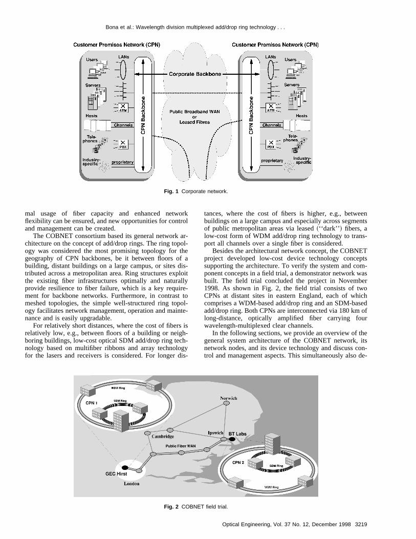
A customer-premises network~CPN!, also referred to as acampus network, interconnects all customer premiequipment, such as private telecommunication, data cmunication and data processing equipment, within a sinsite of an organization. Corporate networks are private nworks that typically comprise multiple CPNs interconected via the public wide-area network~WAN! or vialines leased from public or private network providers~seeFig. 1!. Corporate networks may cover a wide geographirange from a single campus to a metropolitan area upglobal dimensions.
In the past, electronic technologies and copper medominated in CPNs. Optical technologies were rarelyplied and only in the form of simple, single-channel tranmission systems. In the foreseeable future, this is notpected to change significantly in the access area of Cwhere classical LAN, asynchronous transfer mode~ATM !and internet protocol~IP! technologies will dominate. Thebackbone of future CPNs, however, and the metropoland wide-area CPN interconnection, which together fothe corporate backbone, will require more advanced opttechnologies capable of coping with the huge amountconcentrated traffic caused by the proliferation of multimdia applications, the Internet/intranet traffic explosion, aby an enormous demand for high-capacity data exchabetween corporate data and storage centers.
Optical networking technologies suited for such futubackbones are the evolving multichannel technologies sas wavelength division multiplexing~WDM! and opticalspace-division multiplexing~SDM!. The key advantages o
3218 Opt. Eng. 37(12) 3218–3228 (December 1998) 0091-3286/98/$
-
-s
l
e
these optical multichannel techniques are that they willable the significant capacity improvements; easy scalaity; and the clear channel connectivity that is essentiaindependent of bit rate, protocol, and—to a larextent—of distance. Within a CPN, clear channels wtransport ATM cells, IP packets, synchronous digihierarchy/synchronous optical network~SDH/SONET! traf-fic, classical and new LAN protocols, computer channprotocols such as Fiber Channel Standard~FCS! or Enter-prise System Connection~ESCON!, as well as digital videoor other industry-specific, proprietary, and future formaOne can even envision clear channels connecting Cacross the future metropolitan and wide-area public nworks.
Critical for the success of optical multichannel technogies in the cost-sensitive private market is the availabiof novel optical components of lower cost than most of tcurrently available components, such as those deployedexample, in the public long-distance WDM market.1,2 Fur-thermore, the network architecture must be adapted tocost/performance capabilities of such new componentsachieve an acceptable overall cost/performance ratio.
Within the framework of the European ACTS researprogram,3 the COBNET~Corporate Optical Backbone Nework! project4,5 was founded to establish the architectuand technological concepts for the next generation of hiperformance corporate networks. These new networks mtake advantage of new and evolving WDM and opticSDM technologies for the backbone while taking into acount the existing switching, multiplexing and routing tecniques such as ATM, SDH/SONET and IP. Thereby op
10.00 © 1998 Society of Photo-Optical Instrumentation Engineers
Bona et al.: Wavelength division multiplexed add/drop ring technology . . .
Fig. 1 Corporate network.
orkrol
ar-ol-
thef ais-loi
llye-t tool-nte
s ish-h-gydis
eenents
s-
ETptsm-as
eroichsedofr
eitson-de-
mal usage of fiber capacity and enhanced netwflexibility can be ensured, and new opportunities for contand management can be created.
The COBNET consortium based its general networkchitecture on the concept of add/drop rings. The ring topogy was considered the most promising topology forgeography of CPN backbones, be it between floors obuilding, distant buildings on a large campus, or sites dtributed across a metropolitan area. Ring structures expthe existing fiber infrastructures optimally and naturaprovide resilience to fiber failure, which is a key requirment for backbone networks. Furthermore, in contrasmeshed topologies, the simple well-structured ring topogy facilitates network management, operation and mainance and is easily upgradable.
For relatively short distances, where the cost of fiberrelatively low, e.g., between floors of a building or neigboring buildings, low-cost optical SDM add/drop ring tecnology based on multifiber ribbons and array technolofor the lasers and receivers is considered. For longer
t
-
-
tances, where the cost of fibers is higher, e.g., betwbuildings on a large campus and especially across segmof public metropolitan areas via leased~‘‘dark’’ ! fibers, alow-cost form of WDM add/drop ring technology to tranport all channels over a single fiber is considered.
Besides the architectural network concept, the COBNproject developed low-cost device technology concesupporting the architecture. To verify the system and coponent concepts in a field trial, a demonstrator network wbuilt. The field trial concluded the project in Novemb1998. As shown in Fig. 2, the field trial consists of twCPNs at distant sites in eastern England, each of whcomprises a WDM-based add/drop ring and an SDM-baadd/drop ring. Both CPNs are interconnected via 180 kmlong-distance, optically amplified fiber carrying fouwavelength-multiplexed clear channels.
In the following sections, we provide an overview of thgeneral system architecture of the COBNET network,network nodes, and its device technology and discuss ctrol and management aspects. This simultaneously also
Fig. 2 COBNET field trial.
3219Optical Engineering, Vol. 37 No. 12, December 1998

Bona et al.: Wavelength division multiplexed add/drop ring technology . . .
Fig. 3 COBNET rings and nodes.
Inartd/idend
isanthgse
e foM
onmallof
angf-anthensor
tri-a
theal-
c-ve
ngthex-achdesay,ndachgh-a-
et-
twoup-ode.
in athen-ul-
-endde,er-ork
he
siblees-
icalllycanthe
for
scribes the demonstrator network built for the field trial.the final section, we focus in more depth on the WDM pof this network and specifically on the deployed WDM addrop component technology based on planar wavegufabricated in high-refractive-index contrast SiON core aSiO2 cladding glass material.
2 System Overview
2.1 General Architecture
The overall structure of a COBNET CPN backboneshown in Fig. 3. Depending on the specific application,optical SDM add/drop ring, a WDM add/drop ring, or bomay be applied, as illustrated. Although both types of rinare physically quite different, they are similar from thlogical, control, and management points of view.
The number of channels per ring is of the order ofN58, . . . ,16~12 in the demonstrator!, which is considered areasonable compromise between cost and performancboth the WDM and the SDM technologies. In the WDcase, this translates into a wavelength spacing of 1.6 nma frequency spacing of 200 GHz within the useful 1550-window. In the SDM case, the single wavelength used inchannels is in the 1300-nm window to enable the uselow-cost laser arrays.
Whereas the total traffic carried in an add/drop ring cbe very high, an individual network node within the rintypically requires only a small portion of the total ring trafic to be dropped and added, namely the one or few chnels that terminate in the corresponding node. Hence,add/drop nodes preferably must be able to bypass all trachannels in the optical domain, to drop and add only onea few channels, and to convert them to or from the eleccal domain. This conceptually simple function offersgood potential for very low cost nodes. However, givenmodest number of wavelengths, the functionality and scability would be very restricted without any higher funtions such as cross-connect possibilities from one wa
3220 Optical Engineering, Vol. 37 No. 12, December 1998
s
r
r
-
it
-
length or space channel to another or between waveleand space channels. Such more complex and relativelypensive functions do not necessarily have to reside in enode. To concentrate them in one or a few high-end nowas found to be a more economical solution. In this wthe majority of ring nodes need only be low-end nodes ahence can be low-cost nodes. Moreover, a hybrid approwas found to be more economical and feasible for the hiend node than an all-optical approach with relatively immture and expensive wavelength conversion technology.
Given the physical structure described, a logical star nwork can be configured on each ring with up toN low-endnodes and one high-end node. Communication betweenlow-end nodes is accomplished in a first hop on anstream wavelength or space channel to the high-end nThere this channel is cross-connected~switched! to a sec-ond downstream wavelength or space channel leadingsecond hop toward the destination node. Furthermore,high-end node itself also has add/drop capability. In cotrast to the low-end nodes, it can even add and drop mtiple channels. Because of this and because the highnode can be reached in a single hop from every other noit is the ideal place to accommodate the shared custompremises equipment such as servers or the public netwinterface unit~PIU!. The latter serves as the gateway to tpublic WAN or to leased~‘‘dark’’ ! fibers provided by apublic or private network provider.
2.2 Scalability and Resilience
For scalability it is easily possible to have multiple ringinterconnected via one high-end node, but it is also possto use multiple high-end nodes within one ring. Both casenable scalability beyondN nodes. The latter case corresponds to mapping multiple logical stars onto one physring. For example, three high-end nodes can be fumeshed via some channels, and the remaining channelsbe reused in each of the three ring segments betweenhigh-end nodes. Scalability is important, but note that

y isgh-
n aof
e,Mtois.ve-s.op-all
’stost-rgelypli-th
nspedNnd
et-erityre-then-pli-
foThes
inere od-for
ofeforeves-heonan
thercuesnelandpo
hatthebelec-ented.ch
thecere-
c-
atnt
uchig-
entorbebethens-calal
ged
eicea-e
ra-to aed
kslsoated-
nd
eenol-
le,fewped,re
rere
nan
Bona et al.: Wavelength division multiplexed add/drop ring technology . . .
the backbones considered, relatively modest scalabilitsufficient. These backbones typically interconnect the hiest hierarchy backbone switches@such as LAN or ATMswitches, and private telephone switchboards~PBXs!#within a CPN or interconnect entire corporate sites withicity. Even in large corporations, the number of eitherthese is not very high.
SDM is by definition the short-distance solution. Hencscalability in terms of distance is not an issue for SDrings. In the case of WDM rings, it may be necessaryapply an optical amplifier if the power budget requires thThe WDM wavelengths have been chosen within the walength window of erbium-doped optical fiber amplifierNevertheless, the COBNET architecture tries to avoidtical amplifiers for cost reasons. This is possible for smnetworks, but in larger networks—with todaytechnology—one or a few amplifiers may be requiredimprove the power budget. Compared to the total invement this is not necessarily a severe drawback in a laWDM network, in contrast to a small network having ona few nodes. Note also that an alternative to optical amfiers is to use additional high-end nodes to regenerateoptical signals. This is especially attractive in locatiowhere additional channels must also be added and drop
One of the key requirements of the COBNET CPbackbone is to provide resilience in the case of fiber acomponent failure. As mentioned, the physical ring nwork naturally provides the means for resilience to fibfailure. The COBNET project has opted for a path-diversconcept using two counter-rotating rings combined withdundancy in transmitting and receiving hardware and/orapplication of optical protection switches. In the demostrator, the low-end node hardware is essentially ducated, although certain compromises have been madecost reasons in the high-end node demonstrator design.requirements leading to the particular decision are highpossible resilience, per-channel protection switching~i.e.,no disturbance of operating channels due to failuresother channels!, lowest possible impact on the ring powbudget, and lowest possible cost. Note that for the sakclarity, the illustrations in this paper and their corresponing descriptions do not show the redundancy requiredhigh availability.
2.3 High-End Cross-Connect Node
A COBNET add/drop ring network consists of a numberlow-end nodes~LENs! and at least one high-end nod~HEN!. As already described, the LENs are designedlowest possible cost and, consequently, cannot exhibitery desirable functionality. The more expensive but necsary functionality is economically concentrated within tCOBNET HEN. Essentially this is the interchange functibetween wavelengths, space channels, or wavelengthspace channels. While performing this interchange,HEN also regenerates the optical signals and blocks cilating optical noise. The HEN is the merging point for thWDM and the SDM ring subnetworks. Additionally, it haan add/drop capability, even for more than one chanHence, the HEN is also the focal point, where serversother shared resources can be connected including theto the public WAN.
e
.
ret
f
-
d
-
.
rt
The COBNET project has reached the conclusion tthe most economical and reliable implementation ofHEN functionality for the foreseeable future shouldbased on a hybrid optoelectronic approach using an etronic high-speed switch in the space domain to implemall of the interchange and add/drop functions mentionThe functional block diagram of the HEN for this approais included in Fig. 3.
On the receive side, the individual wavelengths onupstream WDM fiber ring are demultiplexed into the spadomain and converted to electrical signals by a set ofceivers~WDM RX!. Similarly, the individual signals fromthe upstream WDM fiber ribbon ring are converted to eletrical signals by a second set of arrayed receivers~SDMRX!. For the concept of clear channels it is important ththe retiming function within the receivers be transparewith respect to the bit rate used in the clear channel. Sreceivers have been developed for COBNET. Electrical snals can be arbitrarily switched via a bit-rate-transparelectronic cross-point switch either to other wavelengthsother space channels. Alternatively, if a channel has todropped in the HEN, the corresponding signal canswitched to a user access port where it is adapted tophysical layer properties required by the user. On the tramit side, all electrical signals are converted back to optisignals by a set of laser transmitters for the individuwavelengths on the WDM side~WDM TX ! and by a set ofarrayed laser transmitters on the SDM side~SDM TX!. Thelatter directly drive the downstream SDM fiber ribbon rinwhile the individual wavelength channels are multiplexagain onto the downstream WDM fiber ring via the samtype of device as used for demultiplexing. For this devan arrayed waveguide grating6 was chosen because the plnar silica waveguide technology7 is expected to achieve thcorrect cost/performance ratio for this application.
The physical architecture of the HEN in the demonsttor is modular, i.e., based on several boards plugged incommon backplane. This backplane is an actively switchbackplane that contains the core of the node, a 32332 elec-tronic cross-point switch~AMCC S2025!. The individualboards directly reflect the corresponding functional blocof the block diagram in Fig. 3. The node architecture is amodular from the control point of view. Each board threquires a certain degree of intelligence contains an embded microcontroller responsible for the local control amonitoring functions on that board. A serial bus~RS485!on the backplane is used for intercommunication betwthe distributed microcontrollers and a common box contrler ~see Section 2.6!.
2.4 Low-End Add/Drop Nodes
Inside the add/drop ring, the LEN concept relies on simplow-cost components and modules, enabling one or awavelength or space channels to be added and dropwhile the other channels, i.e., the bulk of the traffic, abeing bypassed.
A functional block diagram of the WDM and the SDMLEN is included in Fig. 3. As mentioned before, they alogically identical although their physical technologies avery different.
The main function of the WDM LEN is provided by aoptical add/drop multiplexer device, also referred to as
3221Optical Engineering, Vol. 37 No. 12, December 1998

kettricththircoson
llyiOt
hatbefewltes tors.m-ulde o
plesub
m-p-
is
theanitte
to
n-on-on-els
vedub-theMH/on-adyH/
H/the
ehesethers,
, inar,
se
h,colen
ent
v-the
nelsandstata
Nnc-its
m-e-
dea-r, a
ofN
irol-
theu-k-
ossat
offandin-nd
el-o-
Bona et al.: Wavelength division multiplexed add/drop ring technology . . .
add/drop filter. Add/drop filters are available on the marin the form of devices based on fiber gratings or dielecfilters. However, although in the COBNET field trial boof these approaches were implemented and tested, aadd/drop approach was also pursued to achieve loweras well as tuning capability. This approach is basedplanar silica waveguide technology, which was initiademonstrated in the form of conventional doped-S2waveguides8 and finally in high-refractive-index contrasSiON waveguide technology~see Section 3!. The tunabilityrange of this approach is sufficiently wide to guarantee tall the wavelengths used in the WDM network canhandled by one type of device. The intrinsic losses of adecibels that can be achieved with the three add/drop fitechnologies considered here enable a number of LENbe used in a ring without the need for optical amplifieThe add/drop filters tested and used in the COBNET deonstrator can add and drop only one channel, but it wobe possible to cascade such components within one nodto design filters capable of adding and dropping multichannels simultaneously, which are then separated in asequent step.
In the case of the SDM LEN, the add/drop element siply is a splice box or, alternatively, an arrangement of otical or optomechanical switches if more flexibilityneeded.
In both LEN cases, the optical channel dropped andone to be added are converted to an electrical signalvice versa in the same type of receiver and laser transmas in the HEN. The electrical add/drop signal is adaptedthe physical layer properties required by the user.
Physically, both LEN types for the field trial are essetially on one board that carries the same type of microctroller as is used in the HEN. These embedded microctrollers communicate via inband communication channwith the box controller of the HEN~see Section 2.6!.
2.5 PIU
The wide-area interconnection of CPNs can be achieacross the public WAN or across leased fibers from a plic or private network provider. In both cases, there areoptions of using either the SDH/SONET layer or a WDlayer. Whereas the SDH/SONET layer is restricted to SDSONET transport, a WDM layer enables clear-channel cnectivity. Across leased fibers, both options are alrepossible today, namely, SDH/SONET via leased SDSONET lines and WDM via plain fibers~dark fibers!. Inthe case of using the public WAN, access at the SDSONET layer is currently possible, while access atWDM layer refers to a future WDM-based WAN.
To connect to a WDM WAN, a PIU is required for thadaptation of CPN channels to WDM WAN channels. Twavelengths used on the WAN side may differ from thoused within the CPN. The PIU essentially is a subset ofHEN using the same type of WDM receivers, transmitteand WDM multiplexer/demultiplexers.
2.6 Control and Management Structure
The control and management aspect of optical networksgeneral, and of the COBNET ring structure, in particulwas well developed within the project.9 All network-relatedinformation is stored in a management information ba
3222 Optical Engineering, Vol. 37 No. 12, December 1998
dt
r
r
-
dr
~MIB !. This MIB is maintained via a layered approacbased on the simple network management proto~SNMP!, a protocol that facilitates communication betwea managed device, the SNMP agent, and a managemapplication, the SNMP manager.
The overall corporate network, possibly comprising seeral CPNs interconnected via a WAN, is managed byCOBNET global manager~see Fig. 4!. The interaction withthe human manager is situated on this level. Clear chancan be set up or taken down from there, and alarmsnotifications are received there. The MIB on this highelevel contains a global view of the system based on daggregation through its different agents.
Each CPN of the corporate network has its own CPagent and manager. This module performs an agent fution for the higher CPN manager, and is a manager inown right for the various nodes in the CPN. This is accoplished via different node MIBs that contain more nodspecific information than the global MIB.
All nodes in the COBNET network have a specific noagent that maintains a node MIB with all relevant informtion for the hierarchical manager. For the demonstratocentralized approach was adopted in which all agentsone CPN are colocated in the box controller of the HEthat is realized by a PC.
All COBNET hardware boards are controlled by thelocal embedded microcontrollers. All these microcontrlers communicate network maintenance messages toagent PC. In the case of the HEN controllers, this commnication is directly via the RS485 control bus on the bacplane. In the case of the LEN controllers, it is done acrthe rings via a low-bandwidth tone modulation carrier this embedded in all optical channels well below the cutfrequency of the data signals. The electronic receivertransmitter chips developed for the COBNET projectclude the corresponding modem circuitry for extraction ainsertion of management communication signals.
2.7 Components
Most key optical and electronic components were devoped specifically for the COBNET project to achieve p
Fig. 4 COBNET control and management structure.

Bona et al.: Wavelength division multiplexed add/drop ring technology . . .
Fig. 5 Planar waveguide WDM multiplexing components used in COBNET: (a) phased array gratingand (b) resonant coupler add/drop.
or
m
eseiveanpovesme
as-hatat-
Mrer-iveon
ensth-theor
c-antinde-tica
cha
s inpo-
a
ticalding
nyatingingostn-devity,oal
ca-ingeof
narre-ow
allyal
rr-tedy.
s-s-d atng-ndtentthe
tentially lower cost than with currently available vendcomponents.10 These key components include
• wavelength stabilized WDM lasers in the 1550-ntelecom window
• SDM 12-channel laser arrays at 1300 nm
• 12-channel laser driver arrays
• WDM 4-channel receiver arrays
• SDM 12-channel receiver arrays
• planar waveguide WDM multiplexer/demultiplexers
• planar waveguide WDM add/drop filters
• SDM 12-channel 132 optical switch arrays.
It is beyond the scope of this paper to describe all thcomponents in detail. Generally, the optoelectrical, actcomponents are characterized by new chip designsnovel packaging techniques. The passive optical comnents are characterized by the use of planar silica waguide technology.7 The fact that optical waveguide devicecan be manufactured by lithographic methods in the saway as very large scale integration~VLSI! chips rendersthem very attractive with regard to cost, compared to clsical, bulk-optical devices. Furthermore, the low losses tcan be achieved with silica waveguide technology aretractive for ring applications.
As an example, the schematic layout of the WDmultiplexer/demultiplexer and the WDM add/drop filter ashown in Fig. 5. The multiplexer/demultiplexer is an arayed waveguide grating consisting of two planar radiatstars interconnected by an array of waveguides with a cstant length difference between adjacent guides. The llike function of the radiative stars and the wavelengdependent phase differences achieved ininterconnecting waveguides make these components wlike a multiplexer and a demultiplexer, respectively.6,11
3 Planar WDM Add/Drop Multiplexer
The planar add/drop filter is built by a cascade of diretional couplers and optical delay lines to form a resoncoupler12 ~RC!. This RC concept, schematically depictedFig. 5~b!, is chosen because of the ability to make thevices tunable via a heater system that modifies the op
d--
--
k
l
path lengths of one of both interconnecting arms of eaMach-Zehnder delay line element. Moreover, it offerslarge degree of design freedom, as is shown later. This imarked contrast to grating-based silica-on-silicon comnents, where the lack of thermo-optic tunability requiresdifferent grating for every wavelength channel.10,13
3.1 High-Refractive-Index Contrast WaveguideTechnology
The device size in standard silica-based integrated opcomponents is an issue because of the minimum benradius of 15 to 20 mm for fiber-matched waveguides.7,12,14
This is particularly important for components having mabent structures such as the phased array waveguide grand the RC. Whereas in the former case well-performmultiplexers can still be made, in the latter case it is almimpossible to fabricate8 more than five stages on a convetional wafer size of, for example, 4 in. Hence, to cascamore stages so as to obtain a better wavelength selectithe structures must be more compact. To achieve this gwe developed a high-refractive-index contrast planar silion-silicon technology using SiON as the core waveguidmaterial.15 It enables the realization of bent waveguidstructures with radii as small as 1.5 mm, i.e., one ordermagnitude smaller than conventional, doped-silica plalightwave structures. Moreover, it meets various requiments such as low loss, polarization insensitivity, and lmanufacturing cost.
The waveguide structures are fabricated onto thermoxidized~9-mm! silicon wafers. Plasma-enhanced chemicvapor deposition~PECVD! is used for the SiON core layeformation. Films with different nitrogen contents and, corespondingly, varying refraction indices can be deposiwith this technique, which is well known in IC technologIn the PECVD process, the gas precursors 2% SiH4 in He,N2O, N2, and optionally NH3 are used. Changing the gaflow ratio modifies the index of refraction. The adeposited films show a large absorption peak centere1508 nm due to the first overtone of the N-H stretchimode at 3375 cm21. The tail of this absorption band extends into the 1550-nm telecommunication window, araises the loss to unacceptably high values. The H conof the film can be reduced substantially by annealing
3223Optical Engineering, Vol. 37 No. 12, December 1998

e.15
tive
n 1of00
theo
linepticthethe
the
, inial-exasiheente-al
ions50
2.
alr asce.M
aef-ce
essa-althe
ro-ters
areith
ingur
in-iallysedde
byion.forareuse
ue.averterve-
to-
aryaonhog-on-e-the
Bona et al.: Wavelength division multiplexed add/drop ring technology . . .
film at 1140°C in a N2 atmosphere. This in turn reduces thpropagation loss for simple slab waveguides to 060.05 dB/cm in the spectral region of interest.
The channel waveguide structure is defined by reacion etching using CHF3 and O2. The design point formonomodal operation and small bending radii betweeand 1.5 mm requires a lateral effective index contrast0.02. Hence, the refractive index of the core layer is 1.5at 1550 nm, and the width and thickness are 3 and 1.94mm,respectively. A 5-mm-thick SiO2 upper cladding layer isdeposited by PECVD. Figure 6 shows a cross section ofwaveguide geometry. Chromium heaters placed on topthe waveguides are used to tune the phase in the delayof the add/drop RC devices by means of the thermo-oeffect, and sputter-deposited aluminum is chosen forlow-resistance contact lines. At the end of the process,chips are diced with a conventional wafer saw, andwaveguide facets are polished to optical quality.
Accurate control of the waveguide parameters andparticular, of the lateral refractive index contrast, is crucfor a well-performing planar lightwave circuit. A wellknown method to determine the lateral refractive indcontrast uses directional couplers, which are also the bbuilding blocks of the RCs. The length required for toptical power to couple from one waveguide to the adjacone is called the coupling length. Its value is directly rlated to the effective refractive index contrast. Directioncouplers were realized with various waveguide separatand lengths. A typical value for the coupling length at 15nm is 2.2 mm for a waveguide separation of 4.3mm. Thiscorresponds well to theoretical calculations15 using a slabmode solver for a lateral effective index contrast of 0.0
Fig. 6 Geometrical dimensions and refractive indices of the planarSiON waveguide structure.
3224 Optical Engineering, Vol. 37 No. 12, December 1998
fs
c
The propagation behavior of the TE and TM opticmodes in the single-mode waveguide must be as similapossible to achieve a negligible polarization dependen7
A difference in the refractive indices for the TE and Tmodes in the planar waveguide structure—birefringence—indeed leads to polarization-dependentfects of the components. In addition to the birefringeninduced by the waveguide geometry of2631024, thereare contributions with opposite signs induced by the strin the layered stack of the waveguiding material. This mjor stress contribution results from the difference in thermexpansion coefficients between the silicon base andsilica layers induced by the thermal treatment during pcessing. Careful optimization of the processing paramelowers the overall birefringence to values,1024, andhence results in polarization-insensitive devices.
3.2 Compact Mode Converters
The high-refractive-index contrast SiON waveguidesmore compact than the standard single-mode fibers wtheir typical core diameter of 9mm. As the optical modesare not matched, conventional fiber-to-chip coupling usflat fiber and chip facets gives rise to high losses. In ocase this butt-coupling loss is about 3.4 dB—which istolerably high. These losses can be reduced substanteither by lensed fibers, but at the expense of increapackaging complexity and cost, or by a spot-size or moconverter. One of the COBNET partners~Italtel Spa! suc-cessfully packaged our chips with lensed fibers, therereducing the coupling losses to about 1 dB per connect
Nevertheless, reducing packaging costs, particularlyapplications in CPN, is mandatory. Mode expandersbelieved to be a good solution because they enable theof the less expensive butt-coupling packaging techniqTo prevent the waste of real estate on the planar lightwcomponents, they must be compact. A spot-size conveimplemented in the form of a nonperiodic segmented waguide structure with irregular tapering can be designedbe as short as 140mm, and improves the waveguide-tofiber coupling efficiency by more than 2 dB per facet.16 Itwas designed and optimized using an evolutionalgorithm.17 The field simulations were performed withsemivectorial 3D finite difference beam propagatimethod~3D FD-BPM!. The short structures obtained witthis approach are simple to integrate in a single-step lithraphy process. An implementation of such a spot-size cverter is shown in Fig. 7. It results in a coupling improvment of 2.1 dB per interface. Reflections induced byconverter are measured to be below240 dB and thereforeare negligible.
Fig. 7 Image of a coupler structure with nonperiodic segments for mode expansion in high-contrastSiON waveguides together with the measured input and output intensity distributions.

ar-ath
de-eita
ng
hasou-ur
ni-e a
prirop
de-ou1.6ata-e
apavebeens
in-by
heofis
ins
esg ao-riesanthe11astm,e is
ropoded,a-ectexted,ossth 1dBthergeonin aor
llol-
terec-de-
Bona et al.: Wavelength division multiplexed add/drop ring technology . . .
3.3 RCs as WDM Add/Drop Filters
A prerequisite to obtain the desired spectral RC filter chacteristic is that the directional coupler parameters, suchseparation and length of the adjacent waveguides andarm length difference of the delay line sections, aresigned properly.15 The RC filter is synthesized with theselements using the standard finite impulse response digfilter theory.18–22 The device response of an RC consistiof N stages can be described by a polynomialF:
F~v!5 (k50
N
bk exp~2 jkvDT!, ~1!
where v is the optical frequency,DT is the delay timedifference in the phase delay arms, andbk is the complexfield amplitude. From the polynomialF, the optical deviceparameters such as the corresponding length of the pshifters as well as the parameters for the directional cplers can be derived as described in Ref. 19. This procedwas implemented in a Labview program that also mimizes the total coupling length. The RC components havperiodic response called a free spectral range~FSR!. Todrop one wavelength channel from a series ofm channels,the FSR must be at leastmDl, whereDl is the channelseparation. The number of stages required for an approate isolation to adjacent wavelength channels to the doutput port can be estimated to be 3/2m for a simple filterdevice design. Figure 8 illustrates two possible devicesigns for a filter that can add and drop one wavelengthof a comb of four channels that are equally spaced bynm ~corresponding to 200-GHz frequency separation1550 nm according to the International Telecommunictions Union grid!. A five-stage device designed with thinterpolated finite impulse response technique18,19,23has thedisadvantage that a narrow notch in the through-pathpears. It demands a perfect match between the laser wlength and the filter device. This critical requirement canrelaxed by broadening the passband notch, at the exp
Fig. 8 Calculated filter characteristic for a one-out-of-four add/dropdevice using a simple design with five stages (dashed line) and awidened design with seven stages (solid line).
se
l
e
e
-
t
--
e
of additional stages. Thereby the number of stagescreases from five to nine, but can be reduced to sevenallowing a smaller isolation for wavelengths other than tfour WDM wavelength channels. In Fig. 8, the wideningthe through path in going from five- to seven-stage filtersclearly demonstrated. Similarly, the drop path contabroad notches to suppress the transit wavelengths.
In a standard doped-SiO2 with SiO2 cladding waveguidetechnology, RC devices with only a small number of stagcan be realized in a line, e.g., five-stage devices havinlength8 of 80 mm. As a first example, we show a compnent that can add and drop one wavelength out of a seof eight with a channel spacing of 3.2 nm. This results inFSR of 25.6 nm. The isolation of the transit channels todrop port was designed to be 30 dB, which requiresstages. Implemented in our high-refractive-index contrtechnology, the device length and width are 52 and 0.8 mrespectively. The measured spectral filter response curvshown in Fig. 9.
As second example, we present a 1-out-of-12 add/dwavelength filter with 1.6-nm wavelength separation. Tobtain the necessary finesse, 16 stages were cascawhich resulted in a total device length of 80 mm. The mesurements shown in Fig. 10 were normalized with respto the transmission of a straight waveguide positioned nto the device. On-chip losses of 3.5 dB were measurwhich consisted of 2.5 dB propagation and 1 dB excess lfor bends and couplers. Using a lensed fiber package widB loss per interface results in a total loss of about 5.5for the RC device. These results nicely demonstrate thatRC design in our SiON technology can be scaled to a lanumber of stages without incurring a significant penaltyinsertion loss. In fact, up to 18 stages can be cascadedsingle line on a 4-in. wafer. If more stages are requiredfor further integration of optical functions, foldedstructures24 can be nicely implemented owing to the smabend radius of 1.5 mm in the high-contrast SiON technogy.
The spectrum shows sharp resonances with a215 dBbandwidth of less than 3.2 nm and an isolation of greathan 15 dB. The sidelobes in the drop transmission sptrum are due to material inhomogeneities along the RC
Fig. 9 Transmission spectrum of an 11-stage RC device measuredover about twice the FSR. It enables selection of one wavelengthout of eight, spaced 3.2 nm apart.
3225Optical Engineering, Vol. 37 No. 12, December 1998

theinterat
e ithee-d tanlaynint-nmtheud-ely
1.6
es.
andin-
bybe
erple-rops. 8
rlyand
ave-edg–ry
ationide,itiv-
ogychsre-t theear
Bona et al.: Wavelength division multiplexed add/drop ring technology . . .
vice. These sidelobes can be minimized by changingrefractive index locally along the waveguides. We showthe next subsection how individually addressed heaelements24,25 on the phase delay branches can compenslocally for imperfections of the filter function.
3.4 Thermo-Optic Tuning and Active DeviceTailoring
As noted, chromium heaters are used to tune the phasthe delay lines of the add/drop devices by means ofthermo-optic effect. The filter characteristic of the RC dvices such as those shown in Figs. 9 and 10 can be tunethe desired add/drop wavelength channel. Typicallyelectrical power of 0.55 W must be applied to each deline heater to tune across one FSR. Figure 11 shows tufor a seven-stage one-out-of-four add/drop filter with flatened passband having a wavelength separation of 1.6The device design, shown in Fig. 8, was described inpreceding subsection. The device length and width, incling the heater contact lines, are 45 and 3 mm, respectiv
Fig. 10 Transmission spectrum of a 16-stage RC device measuredover about twice the FSR. It enables selection of one wavelengthout of 12, spaced 1.6 nm apart.
Fig. 11 Tuning of the filter characteristics over one FSR for aseven-stage one-out-of-four add/drop filter with flattened passbandhaving 1.6-nm wavelength separation. Three filter curves areshown, corresponding to approximately 0, 2, and 4 W total electricalpower.
3226 Optical Engineering, Vol. 37 No. 12, December 1998
e
n
o
g
.
.
To tune to the next wavelength channel, separated bynm, a total electrical power of 1 W and for an FSR about 4W must be applied. Experimentally we found that ththermo-optic switching is accomplished in less than 0.8 m
The filter characteristics, as shown in Figs. 9~11-stagecomponent! and 10~16-stage component!, often have im-perfections such as sidelobes or asymmetric passbandsstop bands. These are mainly caused by phase errorsduced by deposition and etch nonuniformities as well asphotolithographic imperfections. These phase errors cancorrected by individual control of the chromium heatstructures that are also used to tune the device. We immented this on the seven-stage one-out-of-four add/dcomponent with a flattened passband, as shown in Figand 11.
The strength of the individual heater control can cleabe seen in Fig. 12, where the designed, noncorrected,optimized spectral responses are plotted versus the wlength. The correction toward the design curve is realizby a fitting procedure using a standard LevenberMarquardt routine, with the electrical power through eveheater as a free parameter.25
The seven-stage one-out-of-four add/drop filter withflattened passband having 1.6-nm wavelength separahas 2.5 dB on-chip loss. Compared to a straight waveguthe excess loss is less than 1 dB. The polarization sensity was measured to be,0.05 nm in the communicationwindow at 1550 nm.
4 Summary and Conclusion
We presented an overview of the system and technolconcept for future COBNETs. The novelty of the approais the introduction of optical WDM and SDM technologiein the cost-sensitive private market. The focus on costsults in an architecture and in components that represenbest compromise that seems to be achievable in the nterm.
Fig. 12 Thermo-optic tailoring toward the design curve for a seven-stage one-out-of-four add/drop filter with a flattened passband hav-ing 1.6-nm wavelength separation. The electrical power througheach heater stage is optimized for best performance.

re-gh-rebe
gthionn-at-
awog.u-
ethlian.
toin
elsortT
ct-dehe
der
ni-a-nsy,
heTH
-.
fulltel
tble
in/
ted
nd
,’’
op
-
iv-
-
her-
jha,
ntve-
arrat-),cs
edfor
ek,alS3,
k,a
on-
l
ci-
e-
erth-
sint-
r
t-
-fil-
nded
Bona et al.: Wavelength division multiplexed add/drop ring technology . . .
As an example of the low-cost components, we psented WDM add/drop filter devices based on a novel hirefractive-index contrast technology using a SiON colayer. Compact resonant coupler filter devices that cantuned with chromium heaters to any specific wavelenwere fabricated. Measured spectral response deviatfrom the design curve can be corrected by individually tuing the delay stage phase control with the chromium heers.
The COBNET concepts are currently being verified intrial network set up in eastern England. It consists of tCPNs, each consisting of a WDM ring and an SDM rinOne CPN is located on the campus of British Telecommnications ~BT! Laboratories in Ipswich, the other on thcampus of GEC Hirst Laboratories near London. BoCPNs are interconnected across the London East AngNetwork ~LEANet!, spanning a distance of about 180 km
The COBNET trial network is an attractive test beddemonstrate business-oriented broadband applicationsrealistic environment. It provides high-bandwidth channwithin and between CPNs that, in principle, can transpany protocol required by the application. The COBNEconsortium itself, in cooperation with the ACTS projeAMUSE, is verifying the network concept with applications such as video conferencing, corporate video onmand, and PBX interworking, all interconnected over tbroadband infrastructure.
Acknowledgments
This work is supported by the European Commission unthe ACTS research program~AC069!. The partners of theconsortium are Compagnie IBM France, National Techcal University of Athens, Siemens AG, GEC-Marconi Mterials Technology, GPT Ltd., British Telecommunicatioplc, Siemens ATEA, Italtel Spa, Nortel TechnologEidgenossische Technische Hochschule Zu¨rich ~ETH!,Ecole Polytechnique Fe´derale de Lausanne, Universita¨tDortmund, and the IBM Zurich Research Laboratory. Tcompact mode converters were developed jointly with Ein a program supported by the Swiss priority program~KTIproject No. 3046.2!. We acknowledge the invaluable contribution from our colleagues T. Ammer, R. Beyeler, UDrechsel, I. Massarek, and M. Tschudy as well as fruitdiscussions with our partners at the Photonic Unit of ItaSpa, and with D. Wiesmann, M. Spu¨hler, and D. Erni ofETH.
References1. J. P. Ryan, ‘‘WDM: North American deployment trends,’’IEEE
Commun. Mag.36, 40–44~Feb. 1998!.2. E. Lowe, ‘‘Current European WDM deployment trends,’’IEEE Com-
mun. Mag.36, 46–50~Feb. 1998!.3. ACTS 97 Publications, ‘‘Overview,’’ ‘‘Program guide,’’ and ‘‘Projec
summaries,’’ European Commission, ACTS Central Office, availaprinted, on CD-ROM, or online via http://www.infowin.org.
4. ‘‘ACTS AC069 COBNET, corporate optical backbone network,’’Ref. 3, ‘‘Project summaries,’’ or online via http://www.infowin.orgACTS/RUS/PROJECTS/ac069.htm.
5. W. Denzel and B. Meekers, ‘‘Photonics in the backbone of corporanetworks—the ACTS COBNET project,’’ inProc. NOC’97, Part 3,pp. 225–232, IOS Press, Antwerp, Belgium~1997!.
6. M. K. Smit, ‘‘PHASAR-based WDM-devices: principles, design aapplications,’’IEEE J. Select. Top. QE2, 236–250~1996!.
7. Y. P. Li and C. H. Henry, ‘‘Silica-based optical integrated circuitsIEE Proc. Optoelectron.143, 263–280~1996!.
8. D. Di Mola and S. Brunazzi, ‘‘Tunable optical waveguide add/drfilter for multi-wavelength applications,’’ inProc. European Conf. on
s
a
-
Integrated Optics (ECIO ’97), pp. 582–585, OSA, Stockholm, Sweden ~Apr. 1997!.
9. J. Armitage, O. Crochat, and J.-Y. Le Boudec, ‘‘Design of a survable WDM optical network,’’ inProc. INFOCOM’97, IEEE, Kobe,Japan~Apr. 1997!; paper number 2D1 available on CD-ROM published by IEEE Computer Society Press.
10. M. S. Borella, J. P. Jue, D. Banerjee, B. Ramamurthy, and B. Mukjee, ‘‘Optical components for WDM lightwave networks,’’Proc.IEEE 85, 1274–1307~1997!.
11. G. H. B. Thompson, R. Epworth, C. Rogers, S. Day, and S. O‘‘An original low loss and pass-band flattened SiO2 on Si planarwavelength demultiplexer,’’ inProc. Conf. on Optical Fiber Commu-nication (OFC ’97), Technical Digest, p. 77, OSA, IEEE Laser andElectro-Optics Society, and IEEE Communications Society~Feb.1998!.
12. H. H. Yaffe, C. H. Henry, M. H. Serbin, and L. G. Cohen, ‘‘Resonacouplers acting as add-drop filters made with silica-on-silicon waguide technology,’’ IEEE J. Lightwave Technol.12, 1010–1014~1994!.
13. J. Hubner, D. Zauner, and M. Kristensen, ‘‘Low cross talk planmultichannel add-drop multiplexer based on sampled Bragg gings,’’ Proc. Conf. on Optical Fiber Communication (OFC ’97Technical Digest, pp. 249–250, OSA, IEEE Laser and Electro-OptiSociety, and IEEE Communications Society~Feb. 1998!.
14. M. Hoffmann, P. Kopka, and E. Voges, ‘‘Low-loss fiber-matchlow-temperature PECVD waveguides with small-core dimensionsoptical communication systems,’’IEEE Photon. Technol. Lett. 9,1238–1240~1997!.
15. B. J. Offrein, G. L. Bona, R. Germann, F. Krommendijk, I. Massarand H. W. M. Salemink, ‘‘High contrast and low loss SiON opticwaveguides by PECVD,’’ inProc. 1996 Symp. of the IEEE/LEOBenelux Chapter, A. Driessen, R. M. de Ridder, Eds., pp. 290–29Univ. Twente, Enschede, Netherlands~1996!.
16. M. M. Spuhler, B. J. Offrein, G. L. Bona, R. Germann, I. Massareand D. Erni, ‘‘A very short planar silica spot-size converter usingnon-periodic segmented waveguide,’’IEEE J. Lightwave Technol.16,1680–1685~1998!.
17. D. Erni, M. M. Spu¨hler, and J. Fro¨hlich, ‘‘A generalized evolutionaryoptimization procedure applied to waveguide mode treatment in nperiodic optical structures,’’ inProc. European Conf. on IntegratedOptics (ECIO ’97), pp. 218–221, OSA~1997!.
18. M. Kawachi and K. Jinguij, ‘‘Planar lightwave circuits for opticasignal processing,’’ inProc. Conf. on Optical Fiber Communication(OFC ’94), pp. 281–282, OSA, IEEE Laser and Electro-Optics Soety, and IEEE Communications Society, San Jose, CA~1994!.
19. K. Jinguji and M. Kawachi, ‘‘Synthesis of coherent two-port latticform optical delay-line circuit,’’ IEEE J. Lightwave Technol.13,73–82~1994!.
20. K. Jinguji, N. Takato, A. Sugita, and M. Kawachi, ‘‘Mach-Zehndinterferometer type optical waveguide coupler with wavelengflattened coupling ratio,’’Electron. Lett.26, 1326–1327~1990!.
21. K. Jinguji and M. Kawachi, ‘‘Two-port optical wavelength circuitcomposed of cascaded Mach-Zehnder interferometers with posymmetrical configurations,’’IEEE J. Lightwave Technol.14, 2301–2310 ~1996!.
22. Y. Hida, N. Takato, and K. Jinguji, ‘‘Wavelength division multiplexewith wide passband and stopband for 1.3mm/1.55mm using silica-based planar lightwave circuit,’’Electron. Lett. 31, 1377–1378~1995!.
23. K. Takiguchi, K. Okamoto, S. Suzuki, and Y. Ohmori, ‘‘Planar lighwave circuit optical dispersion equalizer,’’IEEE Photonics Technol.Lett. 6, 86–88~1994!.
24. K. Takiguchi, K. Jinguij, and Y. Ohmori, ‘‘Variable group-delay dispersion equalizer based on a lattice-form programmable opticalter,’’ Electron. Lett.31, 1240–1241~1995!.
25. K. Takiguchi, S. Kawanishi, H. Takara, K. Okamoto, K. Jinguji, aY. Ohmori, ‘‘Higher order dispersion equalizer of dispersion shiftfiber using a lattice-form programmable optical filter,’’Electron. Lett.32, 755–756~1996!.
Gian-Luca Bona studied physics at theSwiss Federal Institute of Technology(ETH), where he received a PhD degree in1987 for his work on short-pulsed laser ex-cited photoemission. After postdoctoralwork at the IBM Zurich Research Labora-tory in the area of picosecond optical sam-pling of ultrafast devices, he became a re-search staff member in 1988, and wasinvolved in work on quantum-well semi-conductor lasers, with an emphasis on the
design and characterization of high-power and short-wavelengthGaAs-based lasers. Since 1994 he has been working on low-cost
3227Optical Engineering, Vol. 37 No. 12, December 1998

Bona et al.: Wavelength division multiplexed add/drop ring technology . . .
planar waveguide components mainly for wavelength division multi-plexed applications. He currently manages the photonic networkingeffort.
Wolfgang E. Denzel received MS andPhD degrees in electrical engineering fromthe University of Stuttgart, Germany, in1979 and 1986, respectively. From 1979to 1985, he was an assistant with the In-stitute of Communications Switching andData Techniques, University of Stuttgart,working in the field of distributed switchingcontrol. In 1985, he joined the researchstaff at the IBM Zurich Research Labora-tory in Ruschlikon, Switzerland. Initially, he
was involved in architectural design and performance analysis ofasynchronous transfer mode (ATM) switches. He assumed respon-sibility for this field in support of the development of IBM’s ATMswitch. From 1990 to 1994, Denzel worked on architectural aspectsof ATM-based customer premises networks and participated in sev-eral European RACE projects in this field. Since 1994, he has beenworking on system aspects of optical networks. He is the technicalcoordinator of the European ACTS project Corporate Optical Back-bone Network (COBNET).
Bert J. Offrein studied applied physics atthe University of Twente, the Netherlands,where he received a PhD degree in 1994.His dissertation examined the measure-ment of optical nonlinearities and the de-sign and realization of an all-opticalswitching device. Since 1995 he has beenwith the optical networking group of theIBM Zurich Research Laboratory, wherehe became a research staff member in1996. His work involves the design and
characterization of optical components for WDM networks.
Roland Germann studied physics at theUniversity of Stuttgart, where he receivedhis PhD in 1990. His dissertation dealswith dry etching of III/V semiconductors forthe fabrication of nanostructures anddistributed-feedback lasers as well as theoptical and electrical characterization ofdry-etch-induced damage. In 1990 he be-came a research staff member with theIBM Zurich Research Laboratory, workingon the fabrication technology of semicon-
ductor lasers for optical data communication and storage applica-
3228 Optical Engineering, Vol. 37 No. 12, December 1998
tions. His current work focuses on the development of optical wave-guide components, such as add/drop filters and (de)multiplexers forwavelength division multiplexing networks. Germann is a member ofthe German Physical Society.
Huub W. M. Salemink received his PhDin superconductivity in 1973 fromNijmegen University, the Netherlands, andhas worked on research topics in opticalapplications in the fields of semiconductorlasers and remote sensing. In 1985, hebecame a research staff member with theIBM Zurich Research Laboratory, workingon the application of tunneling microscopyto study dopant distributions as well as to
analyze semiconductor interfaces and III–V alloys at the atomicscale. Currently, he is engaged in research on materials aspects ofsilicon-oxide-based compounds used in waveguide fabrication.Since 1996, he has been a visiting professor with the FoundationPhysica at the Technical University of Delft, the Netherlands.
Folkert Horst received his MS degree inapplied physics and his PhD degree inelectronics engineering from the Univer-sity of Twente, Enschede, the Nether-lands, in 1992 and 1997, respectively. In1997, he joined the optical networkinggroup of the IBM Zurich Research Labora-tory in Ruschlikon, Switzerland. His cur-rent research involves the design andcharacterization of components for WDMoptical networks based on siliconoxyni-tride technology.


