Embed Size (px)
Citation preview
Willem Dirk van Driel · Oliver Pyper Cornelia Schumann Editors
Sensor Systems SimulationsFrom Concept to Solution

Sensor Systems Simulations
Willem Dirk van Driel • Oliver PyperCornelia SchumannEditors
Sensor Systems Simulations
From Concept to Solution
123

EditorsWillem Dirk van DrielDelft University of TechnologyDelft, The Netherlands
Oliver PyperInfineon Technologies Dresden GmbH &Co. KGDresden, Germany
Cornelia SchumannInfineon Technologies Dresden GmbH &Co. KGDresden, Germany
ISBN 978-3-030-16576-5 ISBN 978-3-030-16577-2 (eBook)https://doi.org/10.1007/978-3-030-16577-2
© Springer Nature Switzerland AG 2020This work is subject to copyright. All rights are reserved by the Publisher, whether the whole or part ofthe material is concerned, specifically the rights of translation, reprinting, reuse of illustrations, recitation,broadcasting, reproduction on microfilms or in any other physical way, and transmission or informationstorage and retrieval, electronic adaptation, computer software, or by similar or dissimilar methodologynow known or hereafter developed.The use of general descriptive names, registered names, trademarks, service marks, etc. in this publicationdoes not imply, even in the absence of a specific statement, that such names are exempt from the relevantprotective laws and regulations and therefore free for general use.The publisher, the authors, and the editors are safe to assume that the advice and information in this bookare believed to be true and accurate at the date of publication. Neither the publisher nor the authors orthe editors give a warranty, express or implied, with respect to the material contained herein or for anyerrors or omissions that may have been made. The publisher remains neutral with regard to jurisdictionalclaims in published maps and institutional affiliations.
This Springer imprint is published by the registered company Springer Nature Switzerland AG.The registered company address is: Gewerbestrasse 11, 6330 Cham, Switzerland

Preface
In this book, we present the results of the European Union project IoSense (seewww.iosense.eu). In this EU project, adequate and verified simulation environ-ments are used to support the predevelopment, development and production rampprocesses for heterogeneous sensor systems. Furthermore, it aims to verify thedeveloped simulation strategies and conduct statistical sensitivity studies using themanufacturing-oriented simulations in order to support principles of design formanufacturability and design for testability (DfM and DfT). Simulations are meansto improve the functional design and/or the processes creating them. The developedsimulation environments will be used to provide application-oriented, multidomain,functional simulations in the area of:
• Device physics and related manufacturability• Multi-level electrical functionality (top level, gate level, module level, device
level, etc.)• Thermal simulations• Energy and power consumption aspects• Other physical domains (pressure, stress, flow, sound, optical/light)• Chemical domains (gas composition, liquid consistency)• Runtime adaptivity and reconfiguration: design, representation and algorithm• Design specifications for self-adaptivity and healing algorithms• Implementation-oriented device simulations (mainly sensors)• Interface between sensor model and device simulation• Definition, modelling and evaluation of the interoperability security concept of
the contactless secure coil-on-chip sensor configuration solution based on NFC(NFC-DIP) according to the defined interfaces of the system specification
This book provides the results of these simulation-based sensor system develop-ments and may be used as a guideline for future sensor integrations concepts.
Delft, The Netherlands Willem Dirk van DrielDresden, Germany Oliver PyperDresden, Germany Cornelia Schumann
v

Acknowledgements
This work was supported by the European Union project “IoSense: FlexibleFE/BE Sensor Pilot Line for the Internet of Everything”. This project has receivedfunding from the Electronic Component Systems for European Leadership JointUndertaking under grant agreement No 692480. This Joint Undertaking receivessupport from the European Unions’ Horizon 2020 research and innovation pro-gramme in Germany, the Netherlands, Spain, Austria, Belgium and Slovakia.
vii
Personal Acknowledgements
Willem van Driel is grateful to his wife, Ruth Doomernik; their two sons, Juul andMats; and their daughter, Lize, for their support on writing and editing this book.The coeditors, Oliver Pyper and Cornelia Schumann, would like to thank Willemvan Driel for his outstanding commitment and energy in compiling this book.Furthermore, our thanks go to all the partners in the project for the great cooperationand, particularly, to the authors of the chapters, who present the achievements in thefield of sensor systems simulations.
March 2019 W. D. van DrielC. Schumann
O. Pyper
ix
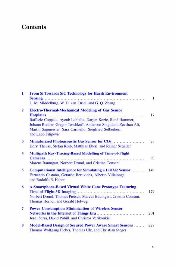
Contents
1 From Si Towards SiC Technology for Harsh EnvironmentSensing . . . . . . . . . . . . . . . . . . . . . . . . . . . . . . . . . . . . . . . . . . . . . . . . . . . . . . . . . . . . . . . . . . . . . . . 1L. M. Middelburg, W. D. van Driel, and G. Q. Zhang
2 Electro-Thermal-Mechanical Modeling of Gas SensorHotplates . . . . . . . . . . . . . . . . . . . . . . . . . . . . . . . . . . . . . . . . . . . . . . . . . . . . . . . . . . . . . . . . . . . . 17Raffaele Coppeta, Ayoub Lahlalia, Darjan Kozic, René Hammer,Johann Riedler, Gregor Toschkoff, Anderson Singulani, Zeeshan Ali,Martin Sagmeister, Sara Carniello, Siegfried Selberherr,and Lado Filipovic
3 Miniaturized Photoacoustic Gas Sensor for CO2 . . . . . . . . . . . . . . . . . . . . . . . 73Horst Theuss, Stefan Kolb, Matthias Eberl, and Rainer Schaller
4 Multipath Ray-Tracing-Based Modelling of Time-of-FlightCameras . . . . . . . . . . . . . . . . . . . . . . . . . . . . . . . . . . . . . . . . . . . . . . . . . . . . . . . . . . . . . . . . . . . . . 93Marcus Baumgart, Norbert Druml, and Cristina Consani
5 Computational Intelligence for Simulating a LiDAR Sensor . . . . . . . . . . 149Fernando Castaño, Gerardo Beruvides, Alberto Villalonga,and Rodolfo E. Haber
6 A Smartphone-Based Virtual White Cane Prototype FeaturingTime-of-Flight 3D Imaging . . . . . . . . . . . . . . . . . . . . . . . . . . . . . . . . . . . . . . . . . . . . . . . . 179Norbert Druml, Thomas Pietsch, Marcus Baumgart, Cristina Consani,Thomas Herndl, and Gerald Holweg
7 Power Consumption Minimization of Wireless SensorNetworks in the Internet of Things Era . . . . . . . . . . . . . . . . . . . . . . . . . . . . . . . . . . 201Jordi Serra, David Pubill, and Christos Verikoukis
8 Model-Based Design of Secured Power Aware Smart Sensors . . . . . . . . 227Thomas Wolfgang Pieber, Thomas Ulz, and Christian Steger
xi
xii Contents
9 A Software Toolkit for Complex Sensor Systems in FogEnvironments . . . . . . . . . . . . . . . . . . . . . . . . . . . . . . . . . . . . . . . . . . . . . . . . . . . . . . . . . . . . . . . 253Dominik Grzelak, Carl Mai, René Schöne, Jan Falkenberg,and Uwe Aßmann
10 Sensor System Optimization Under Uncertainty . . . . . . . . . . . . . . . . . . . . . . . 283Wolfgang Granig, Lisa-Marie Faller, and Hubert Zangl
11 Reliability of IoT Sensor Systems: New Methods forthe Efficient and Comprehensive Reliability Assessment . . . . . . . . . . . . . . 317J. Albrecht, G. Gadhiya, and S. Rzepka
12 Sensor Testing for Smart Mobility Scenarios: From ParkingAssistance to Automated Parking . . . . . . . . . . . . . . . . . . . . . . . . . . . . . . . . . . . . . . . . . 331J. Murgoitio Larrauri, E. D. Martí Muñoz, M. E. Vaca Recalde,B. Hillbrand, A. Tengg, Ch. Pilz, and N. Druml
13 Health Monitoring for Lighting Applications . . . . . . . . . . . . . . . . . . . . . . . . . . . 367W. D. van Driel, L. M. Middelburg, B. El Mansouri,and B. J. C. Jacobs
14 Ultraviolet Sensing in WBG: SiC . . . . . . . . . . . . . . . . . . . . . . . . . . . . . . . . . . . . . . . . . 397B. El Mansouri, W. D. van Driel, and G. Q. Zhang
15 Integrated Photonic Microsystems . . . . . . . . . . . . . . . . . . . . . . . . . . . . . . . . . . . . . . . 427J. Kjellman, N. Hosseini, Jeong Hwan Song, T. Tongnyuy,S. Dwivedi, B. Troia, B. Figeys, S. Kerman, A. Stassen, P. Neutens,S. Severi, R. Jansen, P. Soussan, S. S. Saseendran, A. Marinins,and X. Rottenberg
Index . . . . . . . . . . . . . . . . . . . . . . . . . . . . . . . . . . . . . . . . . . . . . . . . . . . . . . . . . . . . . . . . . . . . . . . . . . . . . . . 449
Chapter 1From Si Towards SiC Technologyfor Harsh Environment Sensing
L. M. Middelburg, W. D. van Driel, and G. Q. Zhang
1.1 Introduction
Since it is obvious that Moore’s Law in its classical way of scaling, which provedto be powerful over the last decades, is coming to an end, alternative routes towardstechnological progress are investigated [1]. One of the main fundamental reasonsfor this is that the smallest features size in newest technology nodes is approachingthe level of only a few atom layers. As a result, the development and implementationof technology nodes based on a scaled-down version of the previous one, getsincreasingly more expensive. An alternative approach to ensure technologicalprogress of the microelectronics world and the semiconductor industry is describedby a trend called “More than Moore” (MtM) [2], based on diversification andintegration. In terms of diversification, materials beyond silicon can be consideredfor the development of sensors and electronics, while the integration aspects cometo expression by combining different parts of a system in a smart and optimal way.Wide bandgap (WBG) materials, such as gallium nitride (GaN) or silicon carbide(SiC) are mature for power applications, but for other applications such as low-voltage (Bi)CMOS and/or VLSI they are still in the research phase. By integratingelectronics monolithically on a sensor chip, improved system performance canbe obtained by having signal amplifications close to the physical transducer. Theintegration aspects are strongly related to the packaging of microelectronic and
L. M. Middelburg · G. Q. ZhangDelft University of Technology, EEMCS Faculty, Delft, The Netherlandse-mail: [email protected]
W. D. van Driel (�)Delft University of Technology, EEMCS Faculty, Delft, The Netherlands
Signify, HTC48, Eindhoven, The Netherlandse-mail: [email protected]; [email protected]
© Springer Nature Switzerland AG 2020W. D. van Driel et al. (eds.), Sensor Systems Simulations,https://doi.org/10.1007/978-3-030-16577-2_1
1
2 L. M. Middelburg et al.
microfabricated devices, for example, when multi-physical sensors are considered.A recent example is the through polymer via enabling an optical channel through apackage [3].
By investigating nonlinear effects in MEMS structures, the mechanical sen-sitivity can be boosted in a bulk micromachined and thus space limited chip.Furthermore, by the application of new materials such as SiC sensors and (lowvoltage) electronics can be yielded compatible with harsh environments and tem-peratures up to 500 ◦C. By investigating the monolithic integration of analogelectronics with mature sensor technologies, the strengths of system integration canbe implemented and exploited, resulting in more value from existing technologies.Especially, the latter two topics are examples of the “More than Moore” concept butstill numerous challenges exist.
The development of SiC-based electronics to build up technologies for low-voltage CMOS, BJTs, or BiCMOS for both analog and digital circuits is stillpre-mature. That this development is still in the research phase is illustrated bythe given that numerous research works focus on device simulation and modelextraction for SiC CMOS. Furthermore, when looking over the literature that isavailable on SiC technology, one could notice a trend in shifting interest from 6H-SiC to 4H-SiC [4–7].
Also, from junction formation by mesa etching on epitaxially grown layers to ionimplantation techniques, which have been evolved during the last 10 years. Otherchallenges on the physical level are the chemical/physical effects in ohmic contactsand the long-term reliability and stability of metallization schemes [8]. So, even onthe very basic physical level significant changes have taken place, illustrating thatthe SiC electronics development is in its pre-mature phase.
In addition to the development of SiC electronics, the compatibility of thefabrication processes is of utmost importance, when all SiC ASIC + MEMSmonolithic system integration are considered. A cleanroom flowchart for theprocessing of MEMS can be very different from one for the processing of electronicsin terms of thermal budget, contamination and topography. Silicon carbide being aharsh environment compatible material, and thus an inert material, involve morefabrication steps such as high temperature processing compared to standard silicontechnology.
1.2 Silicon Technology and Its Limitations
Silicon technology has been mature for decades for the fabrication of a broad rangeof electronics, ranging from BJTs, analog CMOS, BiCMOS to digital integratedcircuits such as VLSI. Based on this silicon technology, sensor technology isimplemented. By reusing existing technologies and process steps such as oxidation,patterning, wet- and dry etching, and dopant formation, big steps are made and apowerful palette of fabrication methods are available for decades. The term “CMOS
1 From Si Towards SiC Technology for Harsh Environment Sensing 3
compatible” is very common in the field of sensors, which practically denotes thatthe sensors considered can be processed within a CMOS process flow, reducingcosts dramatically. It should however be realized that this implicit choice for siliconand CMOS compatible technology can have some dramatic drawbacks in the sensordesign for certain applications. For numerous applications, silicon is not the first-choice material, but is still chosen for its earlier mentioned widespread availability.Furthermore, a CMOS compatible process flow might put restrictions to the sensordesign, negatively influencing overall design freedom and compromising sensorperformance. Surface and bulk micromachining techniques, such as Deep ReactiveIon Etching (DRIE), have been developed based on etching technologies fromsilicon CMOS processing, for example, by extending etch times or increased etchpower in case of plasma etching. This development has enabled the design andrealization of Micro-Electro-Mechanical-Systems (MEMS) in silicon. Currently,the MEMS market covers application field such as Radar, Ultra Sonic, LiDAR,Chemical-, magnetic-, imaging-, and pressure sensors and has a value of aroundten billion dollars [9].
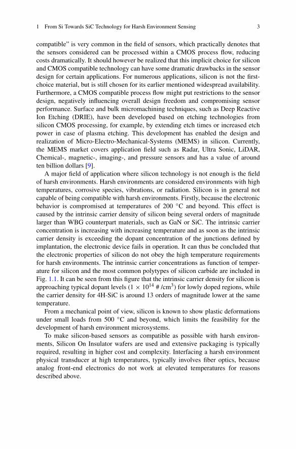
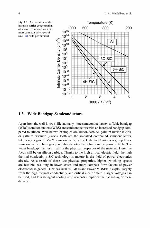
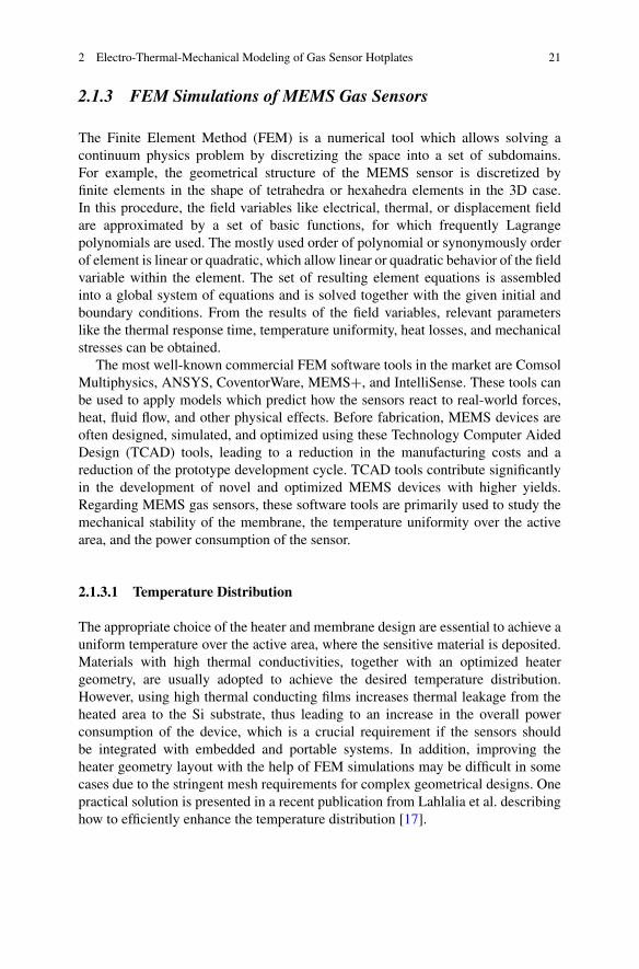
A major field of application where silicon technology is not enough is the fieldof harsh environments. Harsh environments are considered environments with hightemperatures, corrosive species, vibrations, or radiation. Silicon is in general notcapable of being compatible with harsh environments. Firstly, because the electronicbehavior is compromised at temperatures of 200 ◦C and beyond. This effect iscaused by the intrinsic carrier density of silicon being several orders of magnitudelarger than WBG counterpart materials, such as GaN or SiC. The intrinsic carrierconcentration is increasing with increasing temperature and as soon as the intrinsiccarrier density is exceeding the dopant concentration of the junctions defined byimplantation, the electronic device fails in operation. It can thus be concluded thatthe electronic properties of silicon do not obey the high temperature requirementsfor harsh environments. The intrinsic carrier concentrations as function of temper-ature for silicon and the most common polytypes of silicon carbide are included inFig. 1.1. It can be seen from this figure that the intrinsic carrier density for silicon isapproaching typical dopant levels (1 × 10¹⁴ # /cm3) for lowly doped regions, whilethe carrier density for 4H-SiC is around 13 orders of magnitude lower at the sametemperature.
From a mechanical point of view, silicon is known to show plastic deformationsunder small loads from 500 ◦C and beyond, which limits the feasibility for thedevelopment of harsh environment microsystems.
To make silicon-based sensors as compatible as possible with harsh environ-ments, Silicon On Insulator wafers are used and extensive packaging is typicallyrequired, resulting in higher cost and complexity. Interfacing a harsh environmentphysical transducer at high temperatures, typically involves fiber optics, becauseanalog front-end electronics do not work at elevated temperatures for reasonsdescribed above.
4 L. M. Middelburg et al.
Fig. 1.1 An overview of theintrinsic carrier concentrationof silicon, compared with themost common polytypes ofSiC ([8], with permission)
1.3 Wide Bandgap Semiconductors
Apart from the well-known silicon, many more semiconductors exist. Wide bandgap(WBG) semiconductors (WBS) are semiconductors with an increased bandgap com-pared to silicon. Well-known examples are silicon carbide, gallium nitride (GaN),or gallium arsenide (GaAs). Both are the so-called compound semiconductors,SiC being a group IV–IV semiconductor, while GaN and GaAs is a group III–Vsemiconductor. These group number denotes the column in the periodic table. Thewider bandgap manifests itself in the physical properties of the material. Here, thefocus will be on silicon carbide. Thanks to the high critical electric field, the highthermal conductivity SiC technology is mature in the field of power electronicsalready. As a result of these two physical properties, higher switching speedsare feasible, resulting in lower losses and more compact form-factors of powerelectronics in general. Devices such as IGBTs and Power MOSFETs exploit largelyfrom the high thermal conductivity and critical electric field. Larger voltages canbe used, and less stringent cooling requirements simplifies the packaging of thesedevices.
1 From Si Towards SiC Technology for Harsh Environment Sensing 5
1.3.1 Polytypes
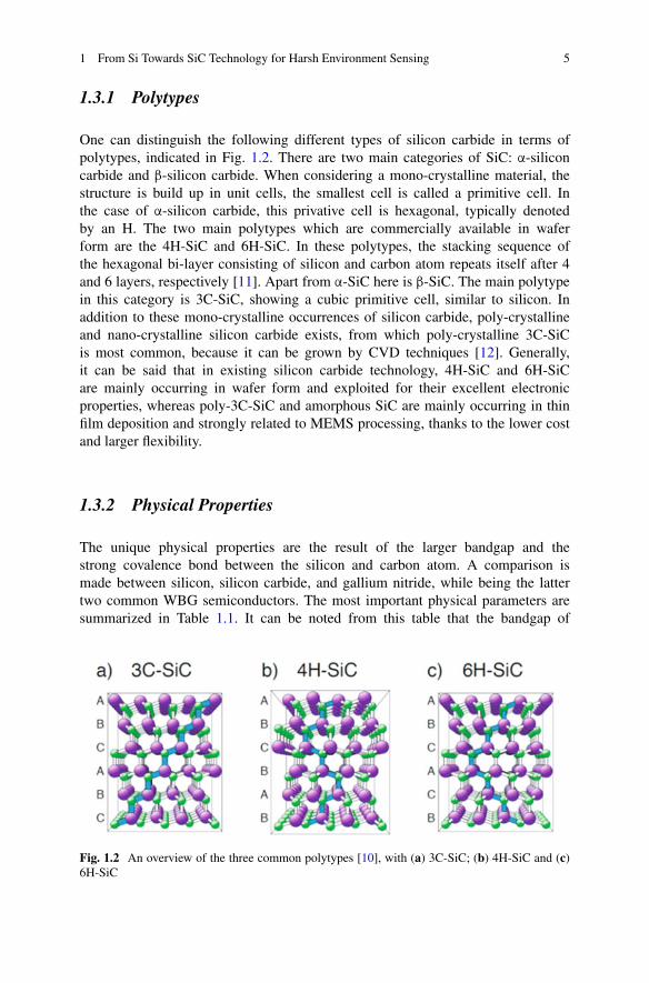
One can distinguish the following different types of silicon carbide in terms ofpolytypes, indicated in Fig. 1.2. There are two main categories of SiC: α-siliconcarbide and β-silicon carbide. When considering a mono-crystalline material, thestructure is build up in unit cells, the smallest cell is called a primitive cell. Inthe case of α-silicon carbide, this privative cell is hexagonal, typically denotedby an H. The two main polytypes which are commercially available in waferform are the 4H-SiC and 6H-SiC. In these polytypes, the stacking sequence ofthe hexagonal bi-layer consisting of silicon and carbon atom repeats itself after 4and 6 layers, respectively [11]. Apart from α-SiC here is β-SiC. The main polytypein this category is 3C-SiC, showing a cubic primitive cell, similar to silicon. Inaddition to these mono-crystalline occurrences of silicon carbide, poly-crystallineand nano-crystalline silicon carbide exists, from which poly-crystalline 3C-SiCis most common, because it can be grown by CVD techniques [12]. Generally,it can be said that in existing silicon carbide technology, 4H-SiC and 6H-SiCare mainly occurring in wafer form and exploited for their excellent electronicproperties, whereas poly-3C-SiC and amorphous SiC are mainly occurring in thinfilm deposition and strongly related to MEMS processing, thanks to the lower costand larger flexibility.
1.3.2 Physical Properties
The unique physical properties are the result of the larger bandgap and thestrong covalence bond between the silicon and carbon atom. A comparison ismade between silicon, silicon carbide, and gallium nitride, while being the lattertwo common WBG semiconductors. The most important physical parameters aresummarized in Table 1.1. It can be noted from this table that the bandgap of
Fig. 1.2 An overview of the three common polytypes [10], with (a) 3C-SiC; (b) 4H-SiC and (c)6H-SiC
6 L. M. Middelburg et al.
Table 1.1 Comparison of physical properties of Si, SiC, and GaN
Figure Unit Si SiC GaN
Bandgap Eg eV 1.12 3.0–3.6a 3.45Maximum electric field Vcm−1 3 × 10⁶ 2.5 × 10⁶ 5 × 10⁶
Relative dielectric constant εr F/m 11.8 9.8 8.9Thermal conductivity Wcm−1 K−1 1.5 4.9 1.5Carrier mobility cm2 V−1 s−1 1350 and 480 980 and 200 1000 and 30Density kgm−3 2330 3210 6150Young’s modulus GPa 62–202 410–700 398Acoustic velocity m/s 8415 13,100 8044
aDepends on polytype
silicon carbide is with 2.3 eV for 3C-SiC, 3.26 eV for 4H-SiC, and 3.03 eVfor 6H-SiC significantly larger than the 1.12 eV of silicon. The larger bandgapdramatically reduces the electron-hole pairs caused by external thermal energy,which reduces leakage currents at elevated temperatures which is one of themajor issues with silicon technology in the application of electronics. The widerbandgap also influences the spectral band where the semiconductor can be usedto detect the light, which will be discussed later onwards. As mentioned abovein the section introduction, silicon carbide shows a high electric breakdown field,1.8–3.8 MV/cm (depending on the polytype) compared to 0.3 MV/cm for silicon[13], which is in combination with its high thermal conductivity advantageousfor power applications. Further, silicon carbide has a high chemical inertnessmaking it an excellent material for transducers in corrosive environments, whileit relaxes stringent packaging requirements. The high Young’s modulus opens newdesign opportunities for the development of silicon carbide MEMS, looking intominiaturization of structures that have mechanically not been feasible in siliconMEMS. This aspect is especially exploitable since it is known that silicon carbideexhibits a piezo-resistive effect [14].
Silicon carbide is moreover known to have a high radiation tolerance, ideal forspace applications [11] and a high acoustic velocity: 11.9 × 10³ ms−1 for SiC vs.9.1 × 103 ms−1 for Si [15].
1.4 Harsh Environment Sensing
As sensors fabricated in silicon carbide technology have advantages in terms ofharsh environment compatibility, in this section the fields and possible applicationsfor such sensors are discussed. Before discussing specific sensor examples, thedefinition of a harsh environment is further specified.

1 From Si Towards SiC Technology for Harsh Environment Sensing 7
1.4.1 Harsh Environments
Because the term harsh environments can be interpreted in different ways, it will bequantified in this section. Harsh environments are seen by this work as environmentswith elevated temperatures. A temperature of 200 ◦C and beyond can already beseen as harsh, silicon-based electronics start to fail namely, but the temperaturerange can even go up to 800 ◦C. Other aspects which make environments harshin this context are the presence of corrosive species (gasses, liquids), vibrations,radiation, and/or a high pressure. Examples of harsh environments include thegeographical poles, very arid deserts, volcanoes, deep ocean trenches, upperatmosphere, Mt. Everest, outer space, and the environments of every planet in theSolar System except the Earth. In applications, examples are boreholes, automobilesunder the hood (motor area), and/or power applications like seen in energy grids.
1.4.2 Overview of Applications
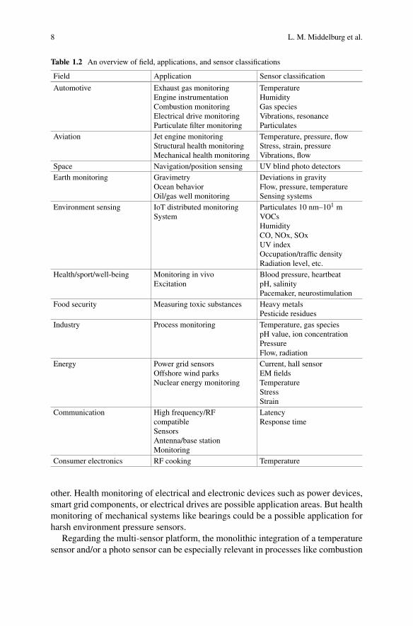
From an application perspective, there are many challenges in our technologicalworld, for example, food security, pollution, global warming, growing demand forenergy, health, and well-being. This results in applications such as environmentalsensing, air quality monitoring, gas sensors for cleaner combustion, sensors for theSmart Grid and Structural and Mechanical Health Monitoring. A more structuredoverview of fields, specific applications, and corresponding sensors is given inTable 1.2.
1.5 Harsh Environment Pressure Sensing
1.5.1 Applications
Numerous applications can be thought of like measurements of absolute pressuresand pressure changes in combustion engines, gas turbines, and jet- and rocketengines. Furthermore, reaction containers and vessels in the industry can beapplications where pressure sensors can have added value when they are harshenvironment compatible. The harsh environments for pressure sensors come most toexpression in applications where both high temperature and corrosive environmentsare included. This is the case in applications where combustion is involved such asaviation jet engines or space applications.
Most pressure sensors consist of a membrane which is basically a transducer of adifference in air pressure to a stress on the membrane. The stress is transferred to astrain by the Young’s modulus and needs to be read out. From this reasoning it couldbe stated that pressure sensors and strain/strain sensors are closely related to each
8 L. M. Middelburg et al.
Table 1.2 An overview of field, applications, and sensor classifications
Field Application Sensor classification
Automotive Exhaust gas monitoringEngine instrumentationCombustion monitoringElectrical drive monitoringParticulate filter monitoring
TemperatureHumidityGas speciesVibrations, resonanceParticulates
Aviation Jet engine monitoringStructural health monitoringMechanical health monitoring
Temperature, pressure, flowStress, strain, pressureVibrations, flow
Space Navigation/position sensing UV blind photo detectorsEarth monitoring Gravimetry
Ocean behaviorOil/gas well monitoring
Deviations in gravityFlow, pressure, temperatureSensing systems
Environment sensing IoT distributed monitoringSystem
Particulates 10 nm–101 mVOCsHumidityCO, NOx, SOxUV indexOccupation/traffic densityRadiation level, etc.
Health/sport/well-being Monitoring in vivoExcitation
Blood pressure, heartbeatpH, salinityPacemaker, neurostimulation
Food security Measuring toxic substances Heavy metalsPesticide residues
Industry Process monitoring Temperature, gas speciespH value, ion concentrationPressureFlow, radiation
Energy Power grid sensorsOffshore wind parksNuclear energy monitoring
Current, hall sensorEM fieldsTemperatureStressStrain
Communication High frequency/RFcompatibleSensorsAntenna/base stationMonitoring
LatencyResponse time
Consumer electronics RF cooking Temperature
other. Health monitoring of electrical and electronic devices such as power devices,smart grid components, or electrical drives are possible application areas. But healthmonitoring of mechanical systems like bearings could be a possible application forharsh environment pressure sensors.
Regarding the multi-sensor platform, the monolithic integration of a temperaturesensor and/or a photo sensor can be especially relevant in processes like combustion

1 From Si Towards SiC Technology for Harsh Environment Sensing 9
Table 1.3 Specifications based on applications
Application Pressure Temperature
Medical 69 mbar [18] 50 ◦COil wells 344 bar [18]Combustion engine 0–100 bar [19] 574 ◦C [20]Geothermal wells 14 bar [16] 350 ◦C [21]Oil and gas exploration 275 ◦CAircraft/turbine engines 1–50 bar [22] −50 up to 650 ◦C [18]Industrial gas turbines 345 bar [18] 450–600 ◦C
monitoring. The integration of multiple sensors on wafer scale, and thus all-SiC hasthe huge advantage of a system which is harsh environment compatible. Regardingthe integration of electronics, this is especially powerful in the application of harshenvironments, since on-chip electronics can modulate and amplify the measuredsignals and can simplify read out of the sensor, which is currently commonly donewith optical fibers. Examples are:
• Combustion monitoring for automotive• Jet engines for aviation• Health monitoring by stress measurement in SiC electronic components, for
example, in electric power domain• Smart grid health monitoring, for example, transformer oil pressure• Pressure measurement on drill-heads for the oil/gas industry• Geothermal wells [16]• Improve jet engine testing (NASA)• Space applications, such as the VENUS project KTH [17]
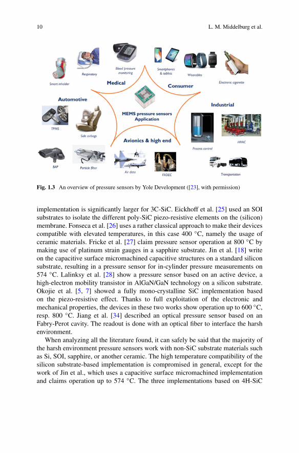
Specification based on applications are listed in Table 1.3 and an overview isdepicted in Fig. 1.3.
1.5.2 State-of-the-Art Harsh Environment Pressure Sensors
For overview and clarity reasons, the found literature is tabulated in Table 1.4. Toidentify each pressure sensor, the substrate material was listed, along with the mainmembrane dimensions and the sensor performance and the transduction type.
Beker et al. [16] write on a surface micromachined circular concentricallymatched capacitive pressure intended for measurements on geothermal wells. Thesubstrate material used was silicon, but the structural layer is poly-crystalline SiC.Chen et al. [19] uses a poly-SiC substrate enabling an all-SiC device. Hung et al.[24] did a comparative study on both mono-crystalline and poly-crystalline SiCand concluded that the gauge factor in the case of a piezo-resistive pressure sensor
10 L. M. Middelburg et al.
Fig. 1.3 An overview of pressure sensors by Yole Development ([23], with permission)
implementation is significantly larger for 3C-SiC. Eickhoff et al. [25] used an SOIsubstrates to isolate the different poly-SiC piezo-resistive elements on the (silicon)membrane. Fonseca et al. [26] uses a rather classical approach to make their devicescompatible with elevated temperatures, in this case 400 ◦C, namely the usage ofceramic materials. Fricke et al. [27] claim pressure sensor operation at 800 ◦C bymaking use of platinum strain gauges in a sapphire substrate. Jin et al. [18] writeon the capacitive surface micromachined capacitive structures on a standard siliconsubstrate, resulting in a pressure sensor for in-cylinder pressure measurements on574 ◦C. Lalinksy et al. [28] show a pressure sensor based on an active device, ahigh-electron mobility transistor in AlGaN/GaN technology on a silicon substrate.Okojie et al. [5, 7] showed a fully mono-crystalline SiC implementation basedon the piezo-resistive effect. Thanks to full exploitation of the electronic andmechanical properties, the devices in these two works show operation up to 600 ◦C,resp. 800 ◦C. Jiang et al. [34] described an optical pressure sensor based on anFabry-Perot cavity. The readout is done with an optical fiber to interface the harshenvironment.
When analyzing all the literature found, it can safely be said that the majority ofthe harsh environment pressure sensors work with non-SiC substrate materials suchas Si, SOI, sapphire, or another ceramic. The high temperature compatibility of thesilicon substrate-based implementation is compromised in general, except for thework of Jin et al., which uses a capacitive surface micromachined implementationand claims operation up to 574 ◦C. The three implementations based on 4H-SiC

1 From Si Towards SiC Technology for Harsh Environment Sensing 11
Tabl
e1.
4A
nov
ervi
ewof
hars
hen
viro
nmen
tpre
ssur
ese
nsor
sin
liter
atur
e
Subs
trat
eT
rans
duct
ion
Mem
bran
eth
ickn
ess
Sens
itivi
tyPr
essu
rera
nge
Tem
p.R
ef
SiC
apac
itive
SiC
-pol
y2
μm
Cir
cula
rR
=12
0μ
m1.
03fF
/kPa
:0–1
.4M
Pa18
0◦C
[16]
Poly
-SiC
Cap
aciti
veSi
C-p
oly
2.8
μm
272
μV
/psi
5M
Pa57
4◦C
[19]
SiPi
ezo-
resi
stiv
epo
ly-S
iC15
μm
177
mV
/V.p
si0.
5M
Pa25
–450
◦ C[2
4]SO
IPi
ezo-
resi
stiv
e3C
SiC
(pol
y)10
0μ
m3.
5m
V/V
.bar
0.35
MPa
200
◦ C[2
5]C
eram
icL
Cta
nkw
.Ant
enna
100
μm
−141
kHz/
bar
10M
Pa40
0◦ C
[26]
Sapp
hire
Ptst
rain
gaug
es20
0μ
m10
μV
/V.b
ar3
MPa
800
◦ C[2
7]Si
Poly
-SiC
capa
citiv
e2.
7μ
m7.
2fF
/psi
574
◦ C[1
8]Si
AlG
aN/G
aNH
EM
T1.
9μ
m1
MPa
[28]
6H-S
iCPi
ezo
resi
stiv
e50
μm
,cir
cula
rR
=60
0μ
m32
.5μ
V/V
.Psi
1.4
MPa
600
◦ C[5
]4H
-SiC
Piez
ore
sist
ive
50μ
m1.
38M
Pa80
0◦ C
[7]
6H-S
iCPi
ezo
resi
stiv
e20
0μ
V/b
ar12
MPa
400
◦ C[2
9]Si
Cap
aciti
ve,m
ono-
3CSi
C0.
5μ
m,c
ircu
lar
R=
400
μm
7.7
fF/to
rr14
6kP
a–23
5kP
a40
0◦ C
[30]
SiC
waf
erC
apac
itive
cavi
ty18
μm
10.6
kHz/
kPa
200
kPa
600
◦ C[3
1]G
aAs
Res
.Tun
neld
iode
1μ
m6
kHz/
kPa
1–50
kPa
Aro
und
RT
[32]
SiPi
ezo-
resi
stiv
e3C
-SiC
poly
30μ
m3.
9m
V/p
si83
kPa
Aro
und
RT
[33]
SiC
SiC
Fabr
y-Pe
rotc
avity
50μ
mci
rcul
arR
=1.
5m
m0.
1–0.
9M
PaR
T[3
4]
12 L. M. Middelburg et al.
and 6H-SiC, respectively, do not describe the etching process or the way themembrane was fabricated or formed. It is known from literature that etching ofmono-crystalline SiC, and silicon carbide in general, is very challenging. Dryetching methods require in general metal hard-masks, which can in turn result inmicromasking issues. Furthermore, the etch rate relatively low, in conventional ICPetchers only up to 500 nm/min [35].
1.6 SiC System Integration: Advantages and Challenges
To fully exploit the advantages of WBG semiconductors in harsh environments,the monolithic integration of readout and communication electronics in SiC is amajor advantage. In this way, both the sensor itself and electronics for readout andthe communication are harsh environment compatible. In order to make the entiresensor system harsh environment compatible, an optical readout can be used tointerface the transducer in its hostile environment [34]. In such a case, conventionalsilicon-based electronics for amplification, processing and further communicationare then placed in less hostile environments.
When electronics can be integrated with the physical transducer, being the sensor,signal amplification can be done directly in the physical location of the transducerby analog front-end electronics, thereby boosting signal power. These electronics donot necessarily have to be complex circuitry, already an output-buffer or relativelysimple differential amplifier can be of great value in terms of increasing signalpower. In this way, noise contributions caused by interference on the interconnect tothe sensor is compromising the analog signal to a smaller extend. This would resultin a significantly increased Signal-to-Noise Ratio (SNR).
When more extensive and complex SiC circuitry is considered, also circuits likedata converters can be considered and an even larger part of the sensor system mightbe integrated in a single chip, including both analog and digital signal processing aswell as communication.
The advantages of monolithic integration lie in the nature of dealing with “one-piece-of-substrate.” Integration on package level typically requires the combinationof multiple dies, yielding the so-called System-in-Package (SiP) solution. Suchan approach requires interconnects between different dies, by for example 3Dpackaging or wire-bonding techniques. Such solutions are undesirable from areliability perspective in case of the applications in harsh environments. DifferentCTEs of the used materials in such a SiP in combination with extremely largetemperature variations and vibrations will influence the durability and reliabilityof such a solution dramatically. When monolithic integration of the ASIC part withthe sensor, i.e., MEMS, part is considered, one dies has to be packaged.
1 From Si Towards SiC Technology for Harsh Environment Sensing 13
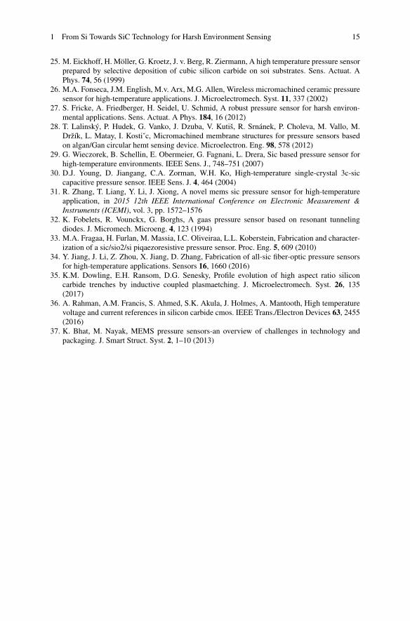
Fig. 1.4 An example from literature for the concept of monolithic integration of a pressuretransducer and readout electronics in silicon [37], with (a) cross-section view, (b) schematic and(c) top view on the IC
Fig. 1.5 The technology roadmap for the SiC pressure sensor platform
Some research is conducted on a CMOS SiC process [36] and the monolithicintegration of front-end electronics with a pressure sensor for silicon technology isdemonstrated in literature, see Fig. 1.4.
The technology roadmap for the SiC pressure sensor platform is indicated inFig. 1.5.

14 L. M. Middelburg et al.
References
1. M.M. Waldrop, The chips are down for Moore’s law. Nature 530, 144 (2016)2. G.Q. Zhang, A. Roosmalen, More than Moore: Creating High Value Micro/Nanoelectronics
Systems (Springer, Berlin, 2009), p. 3303. J. Hamelink, R.H. Poelma, M. Kengen, Through-polymer-via for 3d heterogeneous integration
and packaging, in 2015 IEEE 17th Electronics Packaging and Technology Conference (EPTC),pp. 1–7
4. R.S. Okojie, A.A. Ned, A.D. Kurtz, Operation of 6h-sic pressure sensor at 500c, in TRANS-DUCERS ‘97. 1997 International Conference on Solid-State Sensors and Actuators, Chicago,vol. 2, pp. 1407–1409
5. R. Okojie, G. Saad, G. Beheim, E. Savrun, Characteristics of a hermetic 6h-sic pressure sensorat 600 c, in AIAA Space 2001 Conference and Exposition, (2001), p. 4652
6. R.S. Okojie, D. Lukco, V. Nguyen, E. Savrun, Demonstration of sic pressure sensors at 750c,in Additional Papers and Presentations 2014, (2014), p. 000028
7. R.S. Okojie, D. Lukco, V. Nguyen, E. Savrun, 4h-sic piezoresistive pressure sensors at 800cwith observed sensitivity recovery. IEEE Electron. Device Lett. 36, 174 (2015)
8. T. Kimoto, J.A. Cooper, Fundamentals of Silicon Carbide Technology: Growth, Characteriza-tion, Devices and Applications (Wiley, New York, 2014)
9. Status of the Mems Industry 2018 Market and Technology Report by Yole Développement.https://www.slideshare.net/Yole_Developpement/status-of-the-mems-industry-2018-market-and-technology-report-by-yole-dveloppement
10. M. Wijesundara, R. Azevedo, Silicon Carbide Microsystems for Harsh Environments, vol 22(Springer Science & BusinessMedia, Berlin, 2011)
11. N.G. Wright, A.B. Horsfall, Sic sensors: A review. J. Phys. D. Appl. Phys. 40, 6345 (2007)12. M. Eickhoff, M. Möller, G. Kroetz, M. Stutzmann, Piezoresistive properties of single crys-
talline, polycrystalline, and nanocrystalline n-type 3 c-sic. J. Appl. Phys. 96, 2872 (2004)13. M. Willander, M. Friesel, Q.-u. Wahab, B. Straumal, Silicon carbide and diamond for high
temperature device applications. J. Mater. Sci. Mater. Electron. J. 17(1), 1–25 (2006)14. H.P. Phan, D.V. Dao, K. Nakamura, S. Dimitrijev, N.T. Nguyen, The piezoresistive effect of sic
for mems sensors at high temperatures: A review. J. Microelectromech. Syst. 24, 1663 (2015)15. D.G. Senesky, B. Jamshidi, K.B. Cheng, A.P. Pisano, Harsh environment silicon carbide
sensors for health and performance monitoring of aerospace systems: A review. IEEE Sens.J. 9, 1472 (2009)
16. L. Beker, A. Maralani, L. Lin, A.P. Pisano, A Silicon Carbide differential output pressure sensorby concentrically matched capacitance, in Micro Electro Mechanical Systems (MEMS), 2017IEEE 30th International Conference on (IEEE), (2017), pp. 981–984
17. M. Ericson, J. Silverudd, Design of Measurement Circuits for Sic Experiment: Kth StudentSatellite Mist (2016)
18. S. Jin, S. Rajgopal, M. Mehregany, Silicon carbide pressure sensor for high temperatureand high-pressure applications: Influence of substrate material on performance, in 2011 16thInternational Solid-State Sensors, Actuators and Microsystems Conference, pp. 2026–2029
19. L. Chen, M. Mehregany, A silicon carbide capacitive pressure sensor for in-cylinder pressuremeasurement. Sens. Actuat. A Phys. 145, 2–8 (2008)
20. C. Li, M. Mehregany, A silicon carbide capacitive pressure sensor for high temperatureand harsh environment applications, in TRANSDUCERS 2007–2007 International Solid-StateSensors, Actuators and Microsystems Conference, pp. 2597–2600
21. S. Shao, 4h-Silicon Carbide Pn Diode for Harsh Environment Sensing Applications (2016)22. Flowmeters & pressure sensors. http://www.flowmeters.com/differential-pressure-technology23. Y. Dévellopment, Mems Pressure Sensor 2018—Market & Technologies Report (2018)24. W. Chien-Hung, C.A. Zorman, M. Mehregany, Fabrication and testing of bulk micromachined
silicon carbide piezoresistive pressure sensors for high temperature applications. IEEE Sens. J.6, 316 (2006)
1 From Si Towards SiC Technology for Harsh Environment Sensing 15
25. M. Eickhoff, H. Möller, G. Kroetz, J. v. Berg, R. Ziermann, A high temperature pressure sensorprepared by selective deposition of cubic silicon carbide on soi substrates. Sens. Actuat. APhys. 74, 56 (1999)
26. M.A. Fonseca, J.M. English, M.v. Arx, M.G. Allen, Wireless micromachined ceramic pressuresensor for high-temperature applications. J. Microelectromech. Syst. 11, 337 (2002)
27. S. Fricke, A. Friedberger, H. Seidel, U. Schmid, A robust pressure sensor for harsh environ-mental applications. Sens. Actuat. A Phys. 184, 16 (2012)
28. T. Lalinský, P. Hudek, G. Vanko, J. Dzuba, V. Kutiš, R. Srnánek, P. Choleva, M. Vallo, M.Držík, L. Matay, I. Kostiˇc, Micromachined membrane structures for pressure sensors basedon algan/Gan circular hemt sensing device. Microelectron. Eng. 98, 578 (2012)
29. G. Wieczorek, B. Schellin, E. Obermeier, G. Fagnani, L. Drera, Sic based pressure sensor forhigh-temperature environments. IEEE Sens. J., 748–751 (2007)
30. D.J. Young, D. Jiangang, C.A. Zorman, W.H. Ko, High-temperature single-crystal 3c-siccapacitive pressure sensor. IEEE Sens. J. 4, 464 (2004)
31. R. Zhang, T. Liang, Y. Li, J. Xiong, A novel mems sic pressure sensor for high-temperatureapplication, in 2015 12th IEEE International Conference on Electronic Measurement &Instruments (ICEMI), vol. 3, pp. 1572–1576
32. K. Fobelets, R. Vounckx, G. Borghs, A gaas pressure sensor based on resonant tunnelingdiodes. J. Micromech. Microeng. 4, 123 (1994)
33. M.A. Fragaa, H. Furlan, M. Massia, I.C. Oliveiraa, L.L. Koberstein, Fabrication and character-ization of a sic/sio2/si piqaezoresistive pressure sensor. Proc. Eng. 5, 609 (2010)
34. Y. Jiang, J. Li, Z. Zhou, X. Jiang, D. Zhang, Fabrication of all-sic fiber-optic pressure sensorsfor high-temperature applications. Sensors 16, 1660 (2016)
35. K.M. Dowling, E.H. Ransom, D.G. Senesky, Profile evolution of high aspect ratio siliconcarbide trenches by inductive coupled plasmaetching. J. Microelectromech. Syst. 26, 135(2017)
36. A. Rahman, A.M. Francis, S. Ahmed, S.K. Akula, J. Holmes, A. Mantooth, High temperaturevoltage and current references in silicon carbide cmos. IEEE Trans./Electron Devices 63, 2455(2016)
37. K. Bhat, M. Nayak, MEMS pressure sensors-an overview of challenges in technology andpackaging. J. Smart Struct. Syst. 2, 1–10 (2013)
Chapter 2Electro-Thermal-Mechanical Modelingof Gas Sensor Hotplates
Raffaele Coppeta, Ayoub Lahlalia, Darjan Kozic, René Hammer,Johann Riedler, Gregor Toschkoff, Anderson Singulani, Zeeshan Ali,Martin Sagmeister, Sara Carniello, Siegfried Selberherr, and Lado Filipovic
2.1 Introduction
2.1.1 Historical Overview
Before the application of semiconducting materials and the discovery of gas sensors,canaries were taken into mines as an alarm for the presence of harmful gases, suchas methane, carbon dioxide, and carbon monoxide. A canary is considered to be asongful bird, but it stops singing when exposed to these types of gases, signaling tothe miners to exit the mine immediately.
By the middle of the previous century, it was demonstrated for the first timethat certain semiconducting materials show changing conductivity when exposedto some gas molecules, especially when heated to an elevated temperature [1].Electrical properties of these materials change when the chemical composition ofits ambient gas changes. In the early 1960s, Seyama proposed a gas-sensing devicebased on a thin ZnO film [2]. With a simple electronic circuit, along with a thinfilm-sensitive layer operating at 485◦C, it was demonstrated that the detectionof a variety of gases such as propane, benzene, and hydrogen was possible. In1967, Shaver described a new method to improve the sensing properties of somesemiconducting metal oxide (SMO) materials towards reducing gases by an additionof small amounts of noble metals, namely, platinum, rhodium, iridium, gold, and
R. Coppeta (�) · G. Toschkoff · A. Singulani · Z. Ali · M. Sagmeister · S. Carnielloams AG, Premstaetten, Austriae-mail: [email protected]
A. Lahlalia · S. Selberherr · L. FilipovicInstitute for Microelectronics, TU Wien, Vienna, Austria
D. Kozic · R. Hammer · J. RiedlerMaterials Center Leoben Forschung GmbH, Leoben, Austria
© Springer Nature Switzerland AG 2020W. D. van Driel et al. (eds.), Sensor Systems Simulations,https://doi.org/10.1007/978-3-030-16577-2_2
17
18 R. Coppeta et al.
palladium [3]. Since then, research has intensified for the development of newsensitive materials and micro-hotplates have been designed and optimized with theaim to commercialize the new generation of the SMO gas sensors.
In July 1970, Taguchi filled a patent application in the United States for thefirst SMO gas sensor device dedicated to safety monitoring [4]. A porous SnO2-sensitive thick film was used for this first-generation due to its promising sensingperformance. To further enhance its sensitivity, palladium was added to the sensitivelayer as a metal catalyst. Afterwards, the sensor was commercialized by FigaroInc. in alarms for the detection of flammable gases to prevent fires in domesticresidences.
Over the last five decades, due to the small footprint, low cost, high sensitivity,and fast response time of the SMO gas sensor, the device has been applied ina variety of applications and in different fields, including food and air qualitymonitoring, healthcare, electronic nose, agriculture, and so on [5, 6]. The SMOsensor is able to be integrated into a simple electronic circuit, making the potentialapplication of this technology so widespread that specific needs have arisen, whichmust be satisfied at an industrial level.
Recently, the desire for SMO gas sensors suitable for portable devices suchas smartphones and smartwatches has notably increased. New scaling challengesmust be overcome in order to enable the practical integration into wearable devices.Low power consumption, high selectivity, and high device reliability are the mostcommon issues considered during gas sensor development. A massive research anddevelopment effort is under way to fulfil all the requirements for a good gas sensorperformance. The research activities are divided into two main topics: the electro-thermal-mechanical performance of the micro-hotplates and the sensing capabilityof the sensitive SMO films. This chapter deals with the electro-thermal-mechanicalperformance and modeling of SMO sensors.
2.1.2 MEMS Gas Sensor
2.1.2.1 Definitions
Micro-Electro-Mechanical Systems (MEMS) refers to technologies used to fab-ricate miniaturized integrated devices, which combine mechanical and electro-mechanical elements. They are fabricated using micro-fabrication techniques, suchas thermal oxidation, photolithography, and chemical vapor deposition (CVD). Thephysical size of MEMS devices can range from the nanometer to the millimeterscale. These types of devices are used as actuators, controllers, and even sensorsin the micrometer range, thereby generating effects on the macroscale. It shouldhowever be noted that MEMS devices do not always include mechanical elements;for instance, the SMO gas sensors are fabricated using bulk micromachining, whichis a process used to produce micromachinery or MEMS, but have no moving parts.The SMO gas sensor is included in the MEMS fabrication family with the aim to
2 Electro-Thermal-Mechanical Modeling of Gas Sensor Hotplates 19
reduce the power consumption without using mechanical elements. By forming astatic membrane as a last step during sensor fabrication, the heat losses from theheated area to the substrate are dramatically reduced.
MEMS gas sensors are broadly based on metal oxides such as ZnSnO4, Nb2O5,In2O3, ITO, and CdO. Among these materials SnO2, WO3, and ZnO are the mostcommonly used in the commercial market since they fulfil all the requirements fora good gas-sensing performance at reasonable fabrication costs [7, 8]. The films aredeposited on top of suspended micro-hotplates using a variety of techniques and indifferent forms, namely: thick film, nanobelt, nanotubes, nanowires, thin film, andnanocompound. The operating principle of the MEMS gas sensor relies on heatingthe sensitive material to high temperatures between 250◦C and 550◦C using Jouleheating of an integrated microheater. The working temperature required depends onthe sensitive material used and the target gas species. To enable the adsorption andelectron exchange between the chemical composition of the ambient gas and thesensitive material, the device must operate at elevated temperatures in the presenceof oxygen [9].
2.1.2.2 Significance
The market size of gas sensors for consumer applications is expected to reachUSD 1297 million by 2023, with a 6.83% compound annual growth rate (CAGR)between 2017 and 2023 [10]. This sector is about to experience the highestgrowth rate of the sensor market. The main factors responsible for the growthof this business are increasing pollution regulations laid down by governments indeveloped countries, which mandate the use of gas sensors in potentially hazardousenvironments, increasing the use of MEMS-based sensor worldwide, and raisingawareness of air quality control among users. In May 2018, the World HealthOrganization (WHO) reported that around seven million people die each year, onein eight of total global deaths, as a result of exposure to air pollution [11]. New datareveal that 90% of the world’s population is exposed to fine particles in polluted air,leading to cardiovascular diseases and lung diseases, including heart disease, stroke,lung cancer, respiratory infections, and chronic obstructive pulmonary diseases.Note that, ambient air pollution has caused around 4.2 million deaths, whereashousehold air pollution has caused about 3.8 million deaths in 2017 alone [11].
Today, wearable devices contain a variety of micro-sensors, such as a light sensor,a pressure sensor, a proximity sensor, an inertial sensor, a hall sensor, and manymore. It is very likely that gas sensors will be the next sensor to be integrated inportable devices [12]. Consumer applications are forcing the new generation of gassensors to minimize size, power consumption, and cost, especially with the use ofMEMS technologies. Making gas sensors available to everyone through integrationwith handheld devices, such as smartphones and wrist watches, allows to monitorair quality easily at any time and from anywhere, thus leading to further increasingawareness about the impacts of climate change. Monitoring indoor and outdoor airquality in real time helps improve the health and quality of life of all human beings.
20 R. Coppeta et al.
2.1.2.3 Applications
The detection of gases at an affordable price, low power consumption, and witha fast response time, is essential in numerous high-technology fields. This iswhy the MEMS gas sensor is generating phenomenal interest due to its broadapplication potential in healthcare, military, industry, agriculture, space exploration,cosmetics, and environmental monitoring. Among other requirements for practicalgas-sensing devices, high reliability, low operating temperature, and high selectivityand sensitivity are desired.
One of the major problems faced by gas sensors dedicated to practical applica-tions is to estimate the concentration of a target gas in a realistic ambient, meaningimproved selectivity towards a target gas. Unfortunately, MEMS gas sensors arecharacterized by high sensitivity but have a poor selectivity. To overcome thislimitation, an array of gas sensors is used to form an artificial olfactory system.The so-called electronic-nose (E-nose) gathers multiple gas sensors in the samedevice simultaneously. Each sensitive material is heated to a specific and uniformtemperature, as the sensitivity of metal oxide to gases relies on the operatingtemperature. Measured responses of all sensors are treated using non-parametricanalyses in order to distinguish between gases, thus enhancing the sensor selectivity.
Nowadays, the MEMS gas sensor can be found in different applications acrossthe market. Some of the most significant application fields of this sensor arementioned below.
• Automotive applications: SMO gas sensors can be used to control motorfunctioning and to help reduce the emissions of harmful gases coming fromcombustion engines [13]. Indeed, a special packaging must be conceived fortheses sensors in order to not be influenced by high temperatures in the exhausts.
• Environmental applications: Due to their outstanding features compared to othersensors available in the market, the MEMS gas sensor can also be used tomeasure and monitor trace amounts of volatile organic compounds (VOCs) in theair [14]. In this area, it is necessary to develop a simple and low-priced deviceable to monitor indoor and outdoor air quality.
• Medical applications: MEMS gas sensors can be used for clinical diagnostics.The detection of target gases coming from biochemical processes, taking placein the human body, leads to the rapid diagnosis of several diseases [15]. Theanalyses can be carried out either directly from the patient’s skin or from theirbreath.
• Agricultural applications: To detect rotting fruits and vegetables during storage,MEMS gas sensor can be employed [16].
2 Electro-Thermal-Mechanical Modeling of Gas Sensor Hotplates 21
2.1.3 FEM Simulations of MEMS Gas Sensors
The Finite Element Method (FEM) is a numerical tool which allows solving acontinuum physics problem by discretizing the space into a set of subdomains.For example, the geometrical structure of the MEMS sensor is discretized byfinite elements in the shape of tetrahedra or hexahedra elements in the 3D case.In this procedure, the field variables like electrical, thermal, or displacement fieldare approximated by a set of basic functions, for which frequently Lagrangepolynomials are used. The mostly used order of polynomial or synonymously orderof element is linear or quadratic, which allow linear or quadratic behavior of the fieldvariable within the element. The set of resulting element equations is assembledinto a global system of equations and is solved together with the given initial andboundary conditions. From the results of the field variables, relevant parameterslike the thermal response time, temperature uniformity, heat losses, and mechanicalstresses can be obtained.
The most well-known commercial FEM software tools in the market are ComsolMultiphysics, ANSYS, CoventorWare, MEMS+, and IntelliSense. These tools canbe used to apply models which predict how the sensors react to real-world forces,heat, fluid flow, and other physical effects. Before fabrication, MEMS devices areoften designed, simulated, and optimized using these Technology Computer AidedDesign (TCAD) tools, leading to a reduction in the manufacturing costs and areduction of the prototype development cycle. TCAD tools contribute significantlyin the development of novel and optimized MEMS devices with higher yields.Regarding MEMS gas sensors, these software tools are primarily used to study themechanical stability of the membrane, the temperature uniformity over the activearea, and the power consumption of the sensor.
2.1.3.1 Temperature Distribution
The appropriate choice of the heater and membrane design are essential to achieve auniform temperature over the active area, where the sensitive material is deposited.Materials with high thermal conductivities, together with an optimized heatergeometry, are usually adopted to achieve the desired temperature distribution.However, using high thermal conducting films increases thermal leakage from theheated area to the Si substrate, thus leading to an increase in the overall powerconsumption of the device, which is a crucial requirement if the sensors shouldbe integrated with embedded and portable systems. In addition, improving theheater geometry layout with the help of FEM simulations may be difficult in somecases due to the stringent mesh requirements for complex geometrical designs. Onepractical solution is presented in a recent publication from Lahlalia et al. describinghow to efficiently enhance the temperature distribution [17].
22 R. Coppeta et al.
The authors in [17] managed to improve the temperature uniformity over theactive area without increasing the power consumption of the device. This wasachieved by using a novel design, the so-called dual-hotplate, which is based ona single circular microheater along with two passive micro-hotplates. The operatingprinciple of this novel structure depends on the high thermal conductivity of themicroheater material compared to the membrane materials. It should be noted thata uniform temperature over the active region is a crucial part for baseline stabilitysince a small change in the temperature over the sensitive material leads to baselinedrift, which impacts the accuracy of the gas sensor measurement [18]. To furtherdecrease the heat losses to the substrate, and thereby reduce the power consumptiondown to a few mW, a new membrane shape is implemented in the dual-hotplatesensor. Curved micro-bridges are used instead of simple beams to enlarge thedistance between the active region and the substrate, while preserving the samemembrane size.
2.1.3.2 Thermal Transient Response
The thermal transient response refers to the time consumed to heat up the micro-heater from room temperature Tc to the target temperature Th. It is calculatedfrom a simple expression (2.1), where the actual temperature distribution insidethe sensor is neglected, while the overall thermal resistance Rth and the overallthermal capacitance Cth of the micro-hotplate are taken into account. The heatbalance between the input power Pin, which corresponds to a steady-state heatertemperature Th and heat losses, can be described by
Cth∂T (t)
∂t= Th − Tc
Rth+ Pin. (2.1)
This equation is solved using Fourier and Laplace analysis with boundary conditionsT(t = 0) = Tc and T(t = ∞) = Th. The temperature of the microheater is observed tofollow exponential behavior with
T (t) = (Th − Tc) e− tτ + Tc, (2.2)
where τ = RthCth is the thermal time constant. As can be seen from the previousequations the thermal time constant depends linearly on the thermal resistance andheat capacity. However, a micro-hotplate with materials having a small thermalresistance and low thermal mass will give a faster response. A small heaterexhibits a faster thermal response thanks to the smaller heat capacity, allowingthe microheater to operate at very short pulse times, which reduces the powerconsumption drastically. Note that reducing the sensor’s active area and membranethickness also improves the thermal response time of the micro-hotplate, as the totalheated mass is reduced.
2 Electro-Thermal-Mechanical Modeling of Gas Sensor Hotplates 23
2.1.3.3 Thermal Simulation
After the design and meshing of the MEMS gas sensor geometry within a TCADtool, verification of the thermal performance, including the temperature distribu-tion, thermal response time, temperature gradient, heat losses, and heat exchangebetween the sensor and its environment, are obtained with the help of a designvalidation software. Indeed, measuring these parameters without the help of FEMtools may be quite challenging, especially if the temperatures are changing quickly,or need to be measured inside the sensor. This means that TCAD software withFEM analysis is an indispensable tool to engineers interested in the detailed thermalperformance of their devices.
To model the entire sensor, each part of the structure is represented by a corre-sponding mesh. The proper choice of the mesh is essential to obtaining accurateapproximations. As mentioned earlier, the mesh is a set of elements for whichthe temperature versus time is calculated. Within each element the temperatureis approximated by an ansatz function. One idea is to derive the equation for thetemperature at the nodes, which are the centers of the elements. For this approach,temperature and flow variations within the elements are neglected and the nodetemperature is regarded as representative of the whole element.
This lower order approximation is of linear convergence order. If the heat flowis balanced by the continuity equation of heat energy, we arrive at the finitevolume approach. Another concept is to replace the differential equation within eachelement using finite differences, which is known as the finite-differences method.
All these approaches require equations to be solved at each node at everytemperature, generating a large set of equations, which must be solved. Onealternative for the thermal problem is to describe the thermal parameters by theirelectrical equivalent as shown in Table 2.1. For this lumped thermal network, theequations can be solved analytically. For effortless equation solving, standard circuitanalysis tools such as LTSpice can be used.
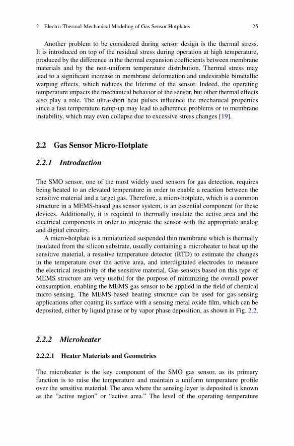
To simulate the heat transfer in a MEMS gas sensor, three mechanisms must besimultaneously taken into account, namely, conduction, convection, and radiation.Generally, radiation is considered to be negligible for temperatures below 600◦C
Table 2.1 Thermal to electric parameter equivalence
Thermal parameter Electrical equivalent
Temperature T (K) Voltage V (V)Specific heat Cp (J/kg K) Permittivity ε (F/m)Thermal resistivity ρth (K m/W) Electric resistivity ρel (� m)Resistance Rth (K/W) Resistance R (� = V/A)Heat flow P (W) Current I (A)Heat Q (J = W s) Charge W (C = A s)Thermal conductivity k (W/K m) Electric conductivity σ (S/m)Capacitance Cth (J/K) Capacitance C (F)

24 R. Coppeta et al.
Fig. 2.1 Heat loss mechanisms through the MEMS gas sensor. Th is the temperature of themicroheater; Ta is the ambient temperature
compared to the heat losses by conduction and convection; heat losses in the MEMSgas sensor are caused mainly by heat conduction through the micro-hotplate and theair, and by heat convection, through heat exchange between the external face of theheated membrane and the surrounding air (Fig. 2.1). It must be noted that the amountof heat lost by convection is proportional to the temperature difference between thesensor surface and the surrounding fluid, and to the area of the face exchanging theheat. In addition, natural convection can only occur in the presence of gravity sinceair movement is dependent on the difference between the specific gravity of coldand hot air. Through this entire discussion, one can deduce that the choice of themembrane and microheater materials and the chosen structure play integral roles indefining the sensor’s power consumption.
2.1.3.4 Mechanical Behavior
The design of an effective and reliable MEMS gas sensor is not only a challengeof having a good thermal performance and high sensing capability but also ofhaving an excellent thermo-mechanical stability. To consider mechanical issuesduring the fabrication stage of the MEMS sensor, one has to analyze the internalstress accumulated in the sensor micro-hotplate. This is one of the major concernsimpacting the performance and long-term mechanical reliability of the device. Inorder to minimize the internal stresses, an appropriate set of process parametersmust be found and the fabrication process must be well controlled. Mechanicalproperties such as density, stoichiometry, orientation, and the average grain sizeof each layer of the sensor are defined by the specific deposition conditions. In thiscontext, it should be noted that the mechanical characteristics of the sensor layerscan be shifted by annealing for one or more cycles. Fortunately, it is possible toadjust these properties by a further annealing step at a specific temperature.
2 Electro-Thermal-Mechanical Modeling of Gas Sensor Hotplates 25
Another problem to be considered during sensor design is the thermal stress.It is introduced on top of the residual stress during operation at high temperature,produced by the difference in the thermal expansion coefficients between membranematerials and by the non-uniform temperature distribution. Thermal stress maylead to a significant increase in membrane deformation and undesirable bimetallicwarping effects, which reduces the lifetime of the sensor. Indeed, the operatingtemperature impacts the mechanical behavior of the sensor, but other thermal effectsalso play a role. The ultra-short heat pulses influence the mechanical propertiessince a fast temperature ramp-up may lead to adherence problems or to membraneinstability, which may even collapse due to excessive stress changes [19].
2.2 Gas Sensor Micro-Hotplate
2.2.1 Introduction
The SMO sensor, one of the most widely used sensors for gas detection, requiresbeing heated to an elevated temperature in order to enable a reaction between thesensitive material and a target gas. Therefore, a micro-hotplate, which is a commonstructure in a MEMS-based gas sensor system, is an essential component for thesedevices. Additionally, it is required to thermally insulate the active area and theelectrical components in order to integrate the sensor with the appropriate analogand digital circuitry.
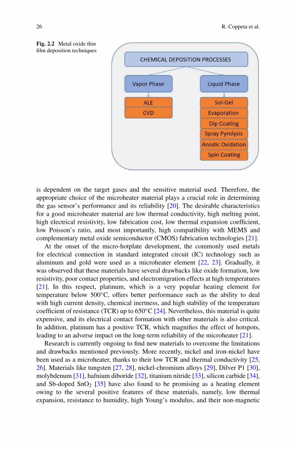
A micro-hotplate is a miniaturized suspended thin membrane which is thermallyinsulated from the silicon substrate, usually containing a microheater to heat up thesensitive material, a resistive temperature detector (RTD) to estimate the changesin the temperature over the active area, and interdigitated electrodes to measurethe electrical resistivity of the sensitive material. Gas sensors based on this type ofMEMS structure are very useful for the purpose of minimizing the overall powerconsumption, enabling the MEMS gas sensor to be applied in the field of chemicalmicro-sensing. The MEMS-based heating structure can be used for gas-sensingapplications after coating its surface with a sensing metal oxide film, which can bedeposited, either by liquid phase or by vapor phase deposition, as shown in Fig. 2.2.
2.2.2 Microheater
2.2.2.1 Heater Materials and Geometries
The microheater is the key component of the SMO gas sensor, as its primaryfunction is to raise the temperature and maintain a uniform temperature profileover the sensitive material. The area where the sensing layer is deposited is knownas the “active region” or “active area.” The level of the operating temperature
26 R. Coppeta et al.
Fig. 2.2 Metal oxide thinfilm deposition techniques
is dependent on the target gases and the sensitive material used. Therefore, theappropriate choice of the microheater material plays a crucial role in determiningthe gas sensor’s performance and its reliability [20]. The desirable characteristicsfor a good microheater material are low thermal conductivity, high melting point,high electrical resistivity, low fabrication cost, low thermal expansion coefficient,low Poisson’s ratio, and most importantly, high compatibility with MEMS andcomplementary metal oxide semiconductor (CMOS) fabrication technologies [21].
At the onset of the micro-hotplate development, the commonly used metalsfor electrical connection in standard integrated circuit (IC) technology such asaluminum and gold were used as a microheater element [22, 23]. Gradually, itwas observed that these materials have several drawbacks like oxide formation, lowresistivity, poor contact properties, and electromigration effects at high temperatures[21]. In this respect, platinum, which is a very popular heating element fortemperature below 500◦C, offers better performance such as the ability to dealwith high current density, chemical inertness, and high stability of the temperaturecoefficient of resistance (TCR) up to 650◦C [24]. Nevertheless, this material is quiteexpensive, and its electrical contact formation with other materials is also critical.In addition, platinum has a positive TCR, which magnifies the effect of hotspots,leading to an adverse impact on the long-term reliability of the microheater [21].
Research is currently ongoing to find new materials to overcome the limitationsand drawbacks mentioned previously. More recently, nickel and iron-nickel havebeen used as a microheater, thanks to their low TCR and thermal conductivity [25,26]. Materials like tungsten [27, 28], nickel-chromium alloys [29], Dilver P1 [30],molybdenum [31], hafnium diboride [32], titanium nitride [33], silicon carbide [34],and Sb-doped SnO2 [35] have also found to be promising as a heating elementowing to the several positive features of these materials, namely, low thermalexpansion, resistance to humidity, high Young’s modulus, and their non-magnetic
2 Electro-Thermal-Mechanical Modeling of Gas Sensor Hotplates 27
nature. Tungsten was reported by Ali et al. [36] as a good high temperature materialfor a heater element. Lahlalia et al. [37] presented a Tantalum-Aluminum (TaAl)layer as a resistive microheater on a perforated membrane in silicon nitride. TaAl ischaracterized by its ability to retain its mechanical strength at high temperature andby its negative TCR of about −100 ppm/◦C, leading to minimal hotspot formationand a stable temperature versus input power curve. The bottom line for choosing aparticular heater material is to fulfil the desired requirements; therefore, there are nosimple design rules. However, the heater geometry plays a critical and active role todefine sensor performance.
Sensitivity, selectivity, and response time are partially dependent on the thermalbehavior of the micro-hotplate. Therefore, the proper choice of the microheaterdesign is a crucial factor in determining the sensing performance of the SMO gassensor. Low power consumption, temperature stability, and temperature uniformityover the sensitive material are three parameters desired while designing the micro-heater element. To achieve the optimal aforementioned requirements, one simplesolution is to alter the microheater geometry. Note that, it is also important toconsider the stress induced in the microheater while testing different geometries.
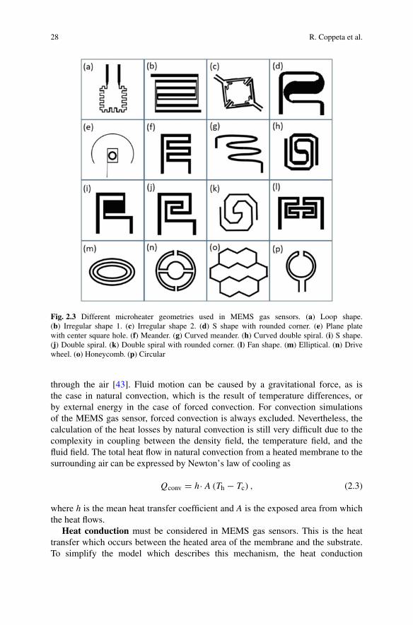
A high stress in the heater element leads to a reduced lifetime of the device.Moreover, current crowding in the corners of the microheater lines is another factorwhich should be taken into account when choosing the geometry of the heaterelement. Localized electron accumulation may lead to the generation of microcracksand localized deformations. To overcome this issue, circular type heater structuresare reported to be a good alternative to conventional microheater geometries suchas the meander shape [38]. Figure 2.3 shows different microheater geometriesinvestigated so far in previous research [39–41].
A new generation of integrated solid-state gas sensors embedded in Siliconon Insulator (SOI) micro-hotplates offer ultra-low power consumption (under100 mW), high sensitivity, low noise, low unit cost, reproducibility, and reliabilitythrough the use of the on-chip integration. The micro-hotplate lies on a SOImembrane and consist of Metal Oxide Semiconductor Field Effect Transistor(MOSFET) heaters which elevate the operating temperature, through self-heating,of a gas-sensitive material. The sensors are fully compatible with SOI CMOS orbiCMOS technologies, In addition, the new integrated sensors offer a nearly uniformtemperature distribution over the active area at its operating temperature at up toabout 300–350◦C. This makes SOI-based gas-sensing devices particularly attractivefor use in hand-held battery-operated gas monitors [42].
2.2.2.2 Heat Losses
MEMS gas sensor-based micro-hotplate dissipates power through three differentmechanisms as already mentioned in Sect. 2.1.3.3.
Free or natural convection is the heat transfer occurring between the heatedsurface of the membrane and the surrounding fluid, including air and other gases.This mechanism is partly described by fluid motion and partly by heat conduction
28 R. Coppeta et al.
Fig. 2.3 Different microheater geometries used in MEMS gas sensors. (a) Loop shape.(b) Irregular shape 1. (c) Irregular shape 2. (d) S shape with rounded corner. (e) Plane platewith center square hole. (f) Meander. (g) Curved meander. (h) Curved double spiral. (i) S shape.(j) Double spiral. (k) Double spiral with rounded corner. (l) Fan shape. (m) Elliptical. (n) Drivewheel. (o) Honeycomb. (p) Circular
through the air [43]. Fluid motion can be caused by a gravitational force, as isthe case in natural convection, which is the result of temperature differences, orby external energy in the case of forced convection. For convection simulationsof the MEMS gas sensor, forced convection is always excluded. Nevertheless, thecalculation of the heat losses by natural convection is still very difficult due to thecomplexity in coupling between the density field, the temperature field, and thefluid field. The total heat flow in natural convection from a heated membrane to thesurrounding air can be expressed by Newton’s law of cooling as
Qconv = h·A (Th − Tc) , (2.3)
where h is the mean heat transfer coefficient and A is the exposed area from whichthe heat flows.
Heat conduction must be considered in MEMS gas sensors. This is the heattransfer which occurs between the heated area of the membrane and the substrate.To simplify the model which describes this mechanism, the heat conduction

2 Electro-Thermal-Mechanical Modeling of Gas Sensor Hotplates 29
perpendicular to the membrane is neglected due to the small thickness of thelayers which compose the membrane stack. This leads to a one-dimensional heatconduction problem in cuboid coordinates. If the entire suspended membrane isheated to a uniform temperature, the heat conduction occurs only in the suspensionbeams. For suspended membranes with three suspension beams, heat losses byconduction can be expressed as
Qcond = 3· λT ·Abeam (Th − Tc)
l. (2.4)
Here, Abeam and l are the sectional area and length of the beam, respectively, andλT is the thermal conductivity of the membrane stack with an n-multilayer system,which can be calculated by
λT =n∑
k=1
λk × tk/
n∑
k=1
tk, (2.5)
where tk is the thickness of the layer k.Radiation is the heat transfer which takes place in the form of electromagnetic
waves primarily in the infrared region. Radiation is emitted by a body as aconsequence of thermal agitation of its composing molecules. In the MEMS gassensor, radiation is considered only on the surface of the heated membrane area asthe radiation emitted from the interior regions can never reach the surface. Underthe assumption that the heated membrane area behaves like a grey body, the heatlosses by radiation can be expressed as
Qrad =∈ σ(T 4
h − T 4c
), (2.6)
where σ is the Stefan–Boltzmann constant, which equals to 5.67 × 10⁻⁸ W/m2K4.For this type of theoretical model, where the frequency-dependent emissivity islower than that of a perfect black body, the emissivity ∈ must be included. Itshould be noted that the heat losses through radiation are often neglected since theyrepresent only a few percent of the total heat losses. Nevertheless, due to the T4
dependency, radiation must be taken into account if the sensor operates at very hightemperatures.
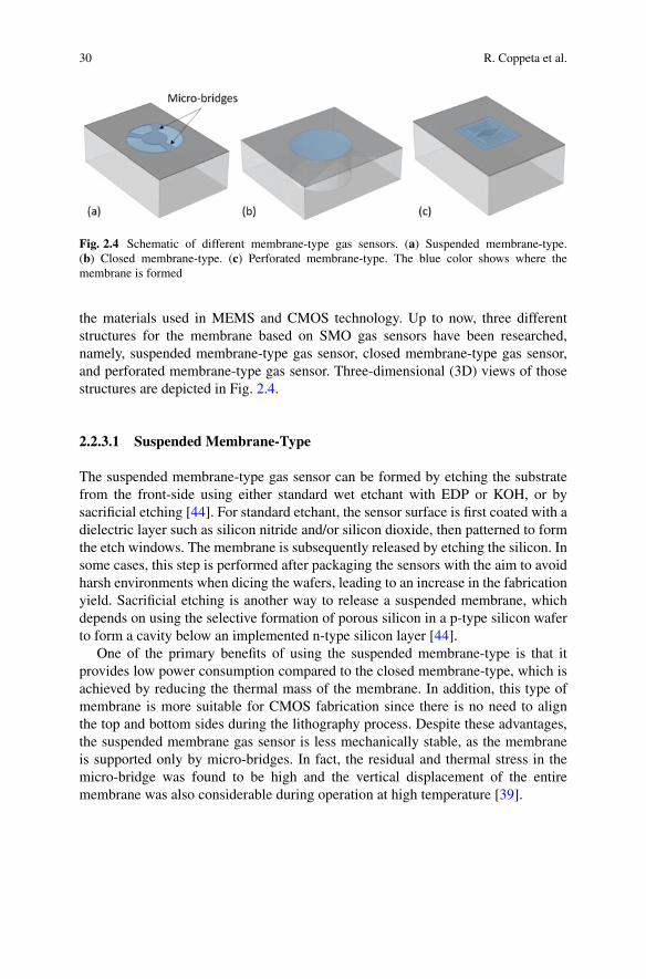
2.2.3 Membrane Types and Materials
In order to achieve a high temperature with low power consumption, differenttypes of the membranes have been adopted instead of using only Si bulk [21].A cavity below the membrane of the gas sensor is essential to minimize thevertical heat losses, as the thermal conductivity of the air is much lower than
30 R. Coppeta et al.
Fig. 2.4 Schematic of different membrane-type gas sensors. (a) Suspended membrane-type.(b) Closed membrane-type. (c) Perforated membrane-type. The blue color shows where themembrane is formed
the materials used in MEMS and CMOS technology. Up to now, three differentstructures for the membrane based on SMO gas sensors have been researched,namely, suspended membrane-type gas sensor, closed membrane-type gas sensor,and perforated membrane-type gas sensor. Three-dimensional (3D) views of thosestructures are depicted in Fig. 2.4.
2.2.3.1 Suspended Membrane-Type
The suspended membrane-type gas sensor can be formed by etching the substratefrom the front-side using either standard wet etchant with EDP or KOH, or bysacrificial etching [44]. For standard etchant, the sensor surface is first coated with adielectric layer such as silicon nitride and/or silicon dioxide, then patterned to formthe etch windows. The membrane is subsequently released by etching the silicon. Insome cases, this step is performed after packaging the sensors with the aim to avoidharsh environments when dicing the wafers, leading to an increase in the fabricationyield. Sacrificial etching is another way to release a suspended membrane, whichdepends on using the selective formation of porous silicon in a p-type silicon waferto form a cavity below an implemented n-type silicon layer [44].
One of the primary benefits of using the suspended membrane-type is that itprovides low power consumption compared to the closed membrane-type, which isachieved by reducing the thermal mass of the membrane. In addition, this type ofmembrane is more suitable for CMOS fabrication since there is no need to alignthe top and bottom sides during the lithography process. Despite these advantages,the suspended membrane gas sensor is less mechanically stable, as the membraneis supported only by micro-bridges. In fact, the residual and thermal stress in themicro-bridge was found to be high and the vertical displacement of the entiremembrane was also considerable during operation at high temperature [39].
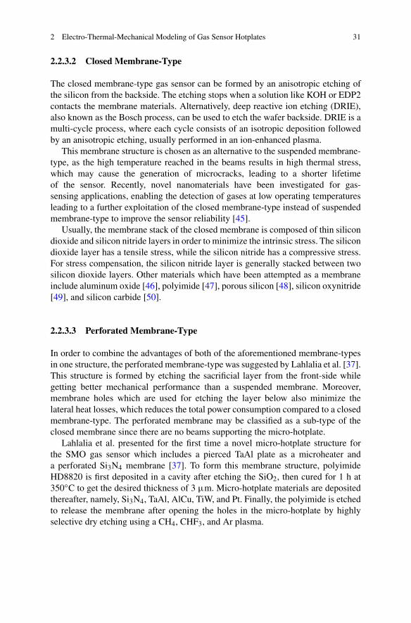
2 Electro-Thermal-Mechanical Modeling of Gas Sensor Hotplates 31
2.2.3.2 Closed Membrane-Type
The closed membrane-type gas sensor can be formed by an anisotropic etching ofthe silicon from the backside. The etching stops when a solution like KOH or EDP2contacts the membrane materials. Alternatively, deep reactive ion etching (DRIE),also known as the Bosch process, can be used to etch the wafer backside. DRIE is amulti-cycle process, where each cycle consists of an isotropic deposition followedby an anisotropic etching, usually performed in an ion-enhanced plasma.
This membrane structure is chosen as an alternative to the suspended membrane-type, as the high temperature reached in the beams results in high thermal stress,which may cause the generation of microcracks, leading to a shorter lifetimeof the sensor. Recently, novel nanomaterials have been investigated for gas-sensing applications, enabling the detection of gases at low operating temperaturesleading to a further exploitation of the closed membrane-type instead of suspendedmembrane-type to improve the sensor reliability [45].
Usually, the membrane stack of the closed membrane is composed of thin silicondioxide and silicon nitride layers in order to minimize the intrinsic stress. The silicondioxide layer has a tensile stress, while the silicon nitride has a compressive stress.For stress compensation, the silicon nitride layer is generally stacked between twosilicon dioxide layers. Other materials which have been attempted as a membraneinclude aluminum oxide [46], polyimide [47], porous silicon [48], silicon oxynitride[49], and silicon carbide [50].
2.2.3.3 Perforated Membrane-Type
In order to combine the advantages of both of the aforementioned membrane-typesin one structure, the perforated membrane-type was suggested by Lahlalia et al. [37].This structure is formed by etching the sacrificial layer from the front-side whilegetting better mechanical performance than a suspended membrane. Moreover,membrane holes which are used for etching the layer below also minimize thelateral heat losses, which reduces the total power consumption compared to a closedmembrane-type. The perforated membrane may be classified as a sub-type of theclosed membrane since there are no beams supporting the micro-hotplate.
Lahlalia et al. presented for the first time a novel micro-hotplate structure forthe SMO gas sensor which includes a pierced TaAl plate as a microheater anda perforated Si3N4 membrane [37]. To form this membrane structure, polyimideHD8820 is first deposited in a cavity after etching the SiO2, then cured for 1 h at350◦C to get the desired thickness of 3 μm. Micro-hotplate materials are depositedthereafter, namely, Si3N4, TaAl, AlCu, TiW, and Pt. Finally, the polyimide is etchedto release the membrane after opening the holes in the micro-hotplate by highlyselective dry etching using a CH4, CHF3, and Ar plasma.
32 R. Coppeta et al.
2.2.4 Electrodes and Thermometer
2.2.4.1 Electrodes
The so-called interdigitated electrodes (IDEs), implemented in the MEMS gassensor, are used to make the measurements of the gas concentration possible. Theseelectrodes have two functions. On one hand, they measure the resistance changein the sensitive layer, which represents the gas concentration. On the other hand,they act as a catalyst when the electrodes are made by noble materials or theiralloys. The catalytic materials promote the interaction between the gas and thesensitive material, leading to an improvement in the sensitivity and response timeof the sensor. Usually, when a thick porous-sensing film is used the electrodes aredeposited below the sensitive material; however, with a thin film-sensitive layer, theyare deposited on top in order to measure the resistance changes on the surface of thesensing layer and to ease the interaction when catalytic electrodes are used. Amongthe most popular materials used for IDEs are gold [51], platinum [52], AlCu [37],and Al [53]. These materials are often deposited with an adhesion layer, such as a20 nm of titanium-tungsten, in order to act as a dielectric, to achieve good adhesion,and to prevent delamination [54].
Another aspect which should be considered when using IDEs for MEMS gassensors is the output signal strength. This is controlled mainly by the design of theactive area, and the pitch of the electrode fingers. The proper design and positioningof the electrodes is essential to maximize the gas sensor response towards desiredgases. It should be noted that it is very important to maintain a uniform temperatureover the IDEs, which must be the same as the microheater temperature for thesensing gases. This can be achieved by forming the microheaters, thermometer, andIDEs in different layers, as the temperature uniformity is better for this combination.Heater and thermometer structures can also be integrated in the same layer withIDEs to ease the fabrication process, but unfortunately, the temperature is lessuniform for this configuration compared with the vertical approach [17, 38].
2.2.4.2 Thermometers
Since the operating temperature of the microheater depends on the target gases andthe sensitive material, an accurate measurement of the micro-hotplate temperatureas a function of the applied power is essential for an optimum performance of theMEMS gas sensor. The extraction of the temperature in these tiny devices is highlychallenging due to the extremely small surfaces of the active region. Moreover, thissurface is often heated to a non-uniform temperature, which impacts the accuracy ofthe measurements. Over the past years, different approaches have been adopted forthis purpose, including simulations, light glowing, RTD, analytical modeling, andthermoreflectance (TR) [55].
2 Electro-Thermal-Mechanical Modeling of Gas Sensor Hotplates 33
Platinum, a commonly used material for the microheater, has also been usedas an RTD since its resistance linearly increases with the temperature [24].Lahlalia et al. used three types of Pt RTDs instead of one [37], deposited onthree different locations over the active region, to additionally characterize thetemperature distribution. To further support the obtained results by Pt RTD, thetemperature was characterized using CrSi as a temperature sensor. This material hasthe ability to detect temperatures above 450◦C by acting as a phase-change material.Hannef et al. experimentally determined the temperature of the micro-hotplate usingTR thermography [27] and proved the accuracy of this method by comparing theobtained results with simulations and silicon RTD.
2.3 Material Properties of Micro-Hotplates
2.3.1 Introduction
In order to achieve the real-world physical performance of the micro-hotplate ina simulation environment, whether relating to power consumption or mechanicalbehavior of the membrane, it is essential to use the correct values for the materialproperties as a function of the operating temperature for all micro-hotplate materials.These material properties can vary due to many factors, such as material thickness,deposition process, and environment conditions. In this section, the main properties,which define the electro-thermal-mechanical performance of the micro-hotplate, arediscussed, namely, thermal conductivity, specific heat capacity, Young’s modulus,and tensile strength.
2.3.2 Thermal Properties
The thermal conductivity and specific heat capacity are the two essential materialproperties which define the capability of a material to store and transfer heat.Understanding these properties is fundamental for devices which experiences rapidchanges in the operating temperature, for any deposition process, or for materialwhich are exposed to large temperature gradients. Precise values for these propertiesare indispensable for micro-hotplate modeling, for heat management to decrease thepower consumption of the device, and for the capability of the device to withstandhigh temperatures and fast temperature changes in the membrane.
34 R. Coppeta et al.
2.3.2.1 Thermal Characterization
Thermal characterization of the materials involved in the MEMS gas sensors iscrucial for understanding the device behavior and for developing physical models,essential for obtaining predictive simulation results.
For thin layers, mainly electrical resistance thermometry (ERT) or laser-basedmethods are used [56, 57]. For ERT, an electrically conductive material, acting as aheater, must be placed on top of the layer of interest. If an electrically conductivelayer has to be characterized, a thin insulating layer must be placed in between.Alternatively, a p-n junction is used as heater and thermometer. For the namedmethods, the general principle is the same. Heat is introduced locally into the sampleby switching a heat source on and off. The transient temperature curve is determinedby the thermal conductivity and the heat capacity.
In the case of ERT, the 3ω method and the thermal impedance are the dominatingmethods. The principle of the 3ω method is that alternating current with frequency ω
is used for heating, which implies that the power, and therefore also the temperature,shows a 2ω modulation. Since electrical resistance is a function of temperature,3ω frequency components show up in the measured voltage. From the latter, thethermal conductivity can be computed using an analytical model [58]. Recently,this principle was also exploited for scanning probe microscopy, where the scanningthermal microscope (SThM) approaches a nanometer resolution [59]. The thermalimpedance method works with the transient temperature response after a steplike switching off of the power of a heater [60]. It also allows to characterizea component’s thermal response and to calibrate the thermal properties of thematerials when an accompanying thermal simulation is performed [61].
In the time-domain thermoreflectance (TDTR) method, a pump laser heats a thinmetallic layer (∼50 nm) on top of the layer of interest. The reflectance of a probelaser is dependent on the temperature. By using fast lasers, e.g., in the picosecondregime, a very fine resolution in time can be obtained. This allows the measurementof very thin layers down to a thickness of a few tens of nanometers. For example,by varying the pump and probe laser spot diameter, the in-plane, as well as outof plane, thermal conductivity can be measured [62]. This method potentially canalso identify the interface conductance and contributions of ballistic transport. Thisis of upmost importance since as layers become thinner and thinner, the system’sbehavior can no longer be described using a bulk thermal conductivity alone.
2.3.2.2 Thermal Modeling
To calculate the heat flux in the micro-hotplate, the thermal conductivity of materialsused must be known, as it provides an indication of the rate at which energy istransferred from the heated area to the substrate. The thermal conductivity dependson the physical structure of matter, which is associated with the state of the matter.From Fourier’s law, the thermal conductivity is expressed as
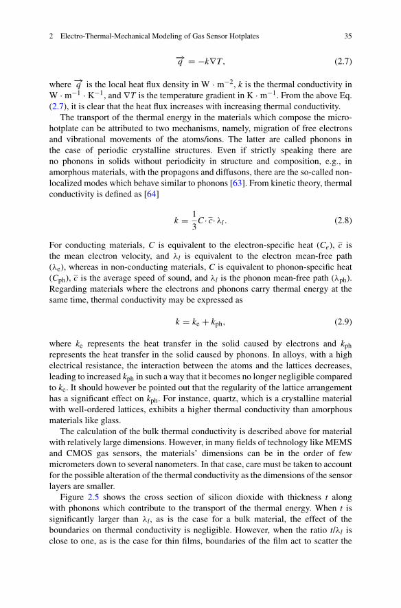
2 Electro-Thermal-Mechanical Modeling of Gas Sensor Hotplates 35
−→q = −k∇T , (2.7)
where −→q is the local heat flux density in W · m−2, k is the thermal conductivity in
W · m−1 · K−1, and ∇T is the temperature gradient in K · m−1. From the above Eq.(2.7), it is clear that the heat flux increases with increasing thermal conductivity.
The transport of the thermal energy in the materials which compose the micro-hotplate can be attributed to two mechanisms, namely, migration of free electronsand vibrational movements of the atoms/ions. The latter are called phonons inthe case of periodic crystalline structures. Even if strictly speaking there areno phonons in solids without periodicity in structure and composition, e.g., inamorphous materials, with the propagons and diffusons, there are the so-called non-localized modes which behave similar to phonons [63]. From kinetic theory, thermalconductivity is defined as [64]
k = 1
3C· c· λl. (2.8)
For conducting materials, C is equivalent to the electron-specific heat (Ce), c isthe mean electron velocity, and λl is equivalent to the electron mean-free path(λe), whereas in non-conducting materials, C is equivalent to phonon-specific heat(Cph), c is the average speed of sound, and λl is the phonon mean-free path (λph).Regarding materials where the electrons and phonons carry thermal energy at thesame time, thermal conductivity may be expressed as
k = ke + kph, (2.9)
where ke represents the heat transfer in the solid caused by electrons and kphrepresents the heat transfer in the solid caused by phonons. In alloys, with a highelectrical resistance, the interaction between the atoms and the lattices decreases,leading to increased kph in such a way that it becomes no longer negligible comparedto ke. It should however be pointed out that the regularity of the lattice arrangementhas a significant effect on kph. For instance, quartz, which is a crystalline materialwith well-ordered lattices, exhibits a higher thermal conductivity than amorphousmaterials like glass.
The calculation of the bulk thermal conductivity is described above for materialwith relatively large dimensions. However, in many fields of technology like MEMSand CMOS gas sensors, the materials’ dimensions can be in the order of fewmicrometers down to several nanometers. In that case, care must be taken to accountfor the possible alteration of the thermal conductivity as the dimensions of the sensorlayers are smaller.
Figure 2.5 shows the cross section of silicon dioxide with thickness t alongwith phonons which contribute to the transport of the thermal energy. When t issignificantly larger than λl, as is the case for a bulk material, the effect of theboundaries on thermal conductivity is negligible. However, when the ratio t/λl isclose to one, as is the case for thin films, boundaries of the film act to scatter the
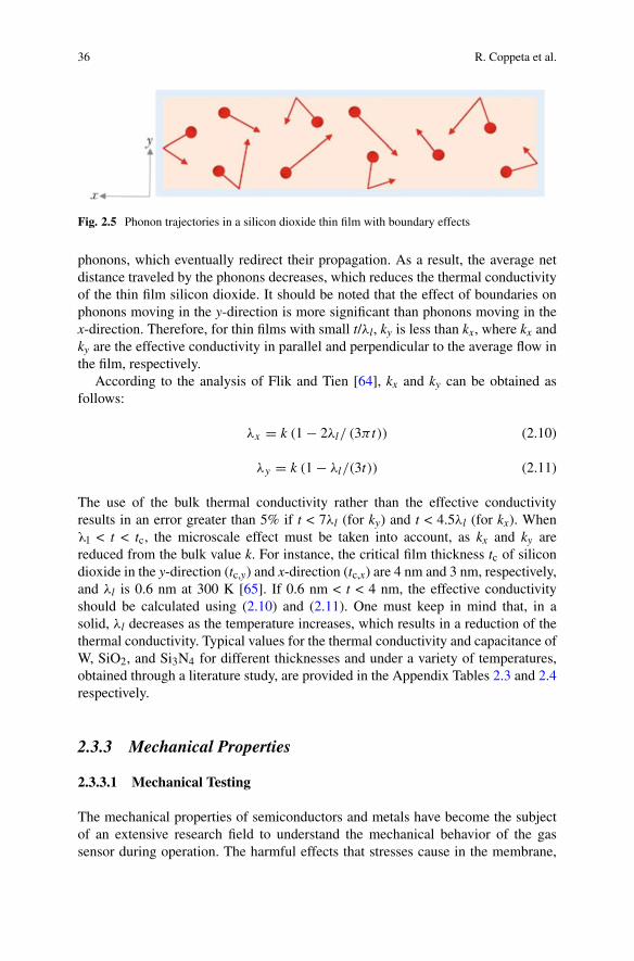
36 R. Coppeta et al.
Fig. 2.5 Phonon trajectories in a silicon dioxide thin film with boundary effects
phonons, which eventually redirect their propagation. As a result, the average netdistance traveled by the phonons decreases, which reduces the thermal conductivityof the thin film silicon dioxide. It should be noted that the effect of boundaries onphonons moving in the y-direction is more significant than phonons moving in thex-direction. Therefore, for thin films with small t/λl, ky is less than kx, where kx andky are the effective conductivity in parallel and perpendicular to the average flow inthe film, respectively.
According to the analysis of Flik and Tien [64], kx and ky can be obtained asfollows:
λx = k (1 − 2λl/ (3πt)) (2.10)
λy = k (1 − λl/(3t)) (2.11)
The use of the bulk thermal conductivity rather than the effective conductivityresults in an error greater than 5% if t < 7λl (for ky) and t < 4.5λl (for kx). Whenλl < t < tc, the microscale effect must be taken into account, as kx and ky arereduced from the bulk value k. For instance, the critical film thickness tc of silicondioxide in the y-direction (tc,y) and x-direction (tc,x) are 4 nm and 3 nm, respectively,and λl is 0.6 nm at 300 K [65]. If 0.6 nm < t < 4 nm, the effective conductivityshould be calculated using (2.10) and (2.11). One must keep in mind that, in asolid, λl decreases as the temperature increases, which results in a reduction of thethermal conductivity. Typical values for the thermal conductivity and capacitance ofW, SiO2, and Si3N4 for different thicknesses and under a variety of temperatures,obtained through a literature study, are provided in the Appendix Tables 2.3 and 2.4respectively.
2.3.3 Mechanical Properties
2.3.3.1 Mechanical Testing
The mechanical properties of semiconductors and metals have become the subjectof an extensive research field to understand the mechanical behavior of the gassensor during operation. The harmful effects that stresses cause in the membrane,
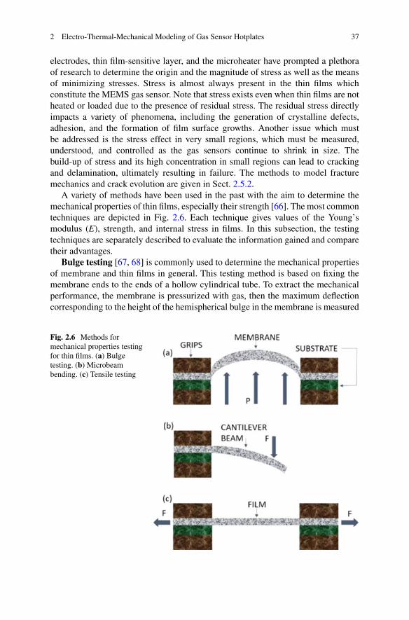
2 Electro-Thermal-Mechanical Modeling of Gas Sensor Hotplates 37
electrodes, thin film-sensitive layer, and the microheater have prompted a plethoraof research to determine the origin and the magnitude of stress as well as the meansof minimizing stresses. Stress is almost always present in the thin films whichconstitute the MEMS gas sensor. Note that stress exists even when thin films are notheated or loaded due to the presence of residual stress. The residual stress directlyimpacts a variety of phenomena, including the generation of crystalline defects,adhesion, and the formation of film surface growths. Another issue which mustbe addressed is the stress effect in very small regions, which must be measured,understood, and controlled as the gas sensors continue to shrink in size. Thebuild-up of stress and its high concentration in small regions can lead to crackingand delamination, ultimately resulting in failure. The methods to model fracturemechanics and crack evolution are given in Sect. 2.5.2.
A variety of methods have been used in the past with the aim to determine themechanical properties of thin films, especially their strength [66]. The most commontechniques are depicted in Fig. 2.6. Each technique gives values of the Young’smodulus (E), strength, and internal stress in films. In this subsection, the testingtechniques are separately described to evaluate the information gained and comparetheir advantages.
Bulge testing [67, 68] is commonly used to determine the mechanical propertiesof membrane and thin films in general. This testing method is based on fixing themembrane ends to the ends of a hollow cylindrical tube. To extract the mechanicalperformance, the membrane is pressurized with gas, then the maximum deflectioncorresponding to the height of the hemispherical bulge in the membrane is measured
Fig. 2.6 Methods formechanical properties testingfor thin films. (a) Bulgetesting. (b) Microbeambending. (c) Tensile testing
38 R. Coppeta et al.
with an interferometer or a microscope and converted to the strain. The equationwhich governs the relationship between the height (h) and the applied differentialpressure (P) is given by
P = 4th
r2
[σi + 2Eh2
3 (1 − v) r2
], (2.12)
where t and r are the thickness of the membrane and specimen radius, respectively;σ i is the residual stress in the membrane under a zero pressure differential, and v isthe Poisson’s ratio.
Microbeam bending or focused ion beam [69–74] is used to extract themechanical properties of the cantilever microbeams, fabricated using microma-chining techniques involving photolithography and etching processes. Typicaldimensions of the beams are smaller than 1 μm thick, 20 μm wide, and 100 μmlong, allowing the cantilever microbeams to be deposited at different locations onthe wafer. This allows for a local monitoring of stress variations in subsequentlydeposited thin films. To determine the Young’s modulus and the yield strengths ofthe thin film materials which comprise the cantilever beam, load–deflection dataalong with beam theory are used. This data are obtained with the aid of a submicronindentation instrument which continuously monitors the load and deflection causedby a nanoindenter [69].
Tensile testing [75, 76] is used to determine how materials will behave undera tension load in order to evaluate both the elastic and plastic response of thinfilms. In a simple tensile test, a thin film is typically pulled to its breaking pointto extract the ultimate tensile strength of the material. The amount of force (F)applied to the extremities of the thin film sample and the elongation (L) of thesample are measured during the experiment. Note that the force is applied byelectromagnetic force transducers, and the elongations are generally measured byoptical methods. In micro-tensile testing, an electron microscope is used to enable adirect observation of the defects during straining. Mechanical properties of materialsare often expressed in terms of stress (σ ), which is the force per unit area, and strain(ε), which is the percent change in length. To obtain the stress, the applied forceis divided by the thin film’s cross-sectional area (σ = F/A). Strain is measured bydividing the change in length by the initial length of the sample (ε = ΔL/L). Thenumerical values of stress and strain can then be presented as a graph called a stress–strain curve.
2.3.3.2 Thermal Stress
The thermal effect is another issue which contributes dramatically to the filmstress. Films heated to high temperatures and then cooled to room temperaturewill experience a thermal stress. Films which are cooled from room temperatureto cryogenic temperatures or thermally cycled will also be thermally stressed. Themagnitude of the thermal stress can be expressed as

2 Electro-Thermal-Mechanical Modeling of Gas Sensor Hotplates 39
σ = Eα (T − T0) , (2.13)
where α is the coefficient of thermal expansion, and T − T0 is the temperaturedifference.
For bilayer combinations such as film/substrate, the strain in the film and thesubstrate are, respectively, expressed by
εfilm = αfilmT + Ffilm (1 − vfilm) / (Efilmtfilmw) , (2.14)
εsub = αsubT + Ffilm (1 − vsub) / (Esubtsubw) , (2.15)
where Ffilm is the thermal mismatch force, w is the width, and t is the thickness.When the strain of film and substrate are identical εfilm = εsub, Ffilm can be obtainedby
Ffilm = w (αsubαfilm) T/
{1 − vfilm
tfilmEfilm+ 1 − vsub
tsubEsub
}. (2.16)
In the case tsubEsub1 − vsub � tfilmEfilm
1 − vfilm, the thermal stress in the film can beexpressed as
σfilm(T ) = Ffilm
tfilmw= (αsub − αfilm) T Efilm
1 − vfilm. (2.17)
It should however be noted that the signs are consistent with dimensional changesin the film and substrate. In the case of αfilm < αsub, thin films prepared at hightemperature will be residually compressed when measured at ambient temperature,as the film shrinks less than the substrate.
2.3.3.3 Intrinsic Stress
Thin film deposition techniques are widely used for the fabrication of the compo-nents of the SMO gas sensors, including microheater, membrane, sensitive layer,insulation layer, and electrodes. During deposition of these thin components, anintrinsic stress σ i is generated, which, in combination with the unavoidable thermalstress, σ film(T), forms the internal or the so-called residual stress (σ film). Thus toextract σ i, the thermal stress given in (2.17) must be subtracted from the measuredvalue of σ film.
Over the past 40 years, the intrinsic stress has prompted scientists to search fora universal explanation of their origins. According to Dorner and Nix [77], theintrinsic stress observed in thin films comes from the following main sources:
Grain Growth Intrinsic stress (compressive stress) in a thin granular film is builtup by grain growth, which occurs by normal boundary migration when the initialgrain is below the critical value in terms of size [78]. Small islands of depositingfilm form on the layer below and as they grow, stress builds up at their interfaces.

40 R. Coppeta et al.
Grain Coalescence During the thin film growth, cohesion starts to occur betweenthe islands as they grow and the gaps between them are small enough, making theparticipating islands elastically strained, which causes a tensile stress in the thin film[79]. This process creates grain boundaries in the film.
Annihilation of Excess Vacancies Intrinsic stress (tensile stress) also builds up dueto the gaps caused by vacancy annihilation at grain boundaries and inside grains. Agap in matter causes atoms in the crystals to move towards each other in order to fillthis void, leading to a planar contraction in the thin film, if it is not deposited on thesubstrate. Otherwise, the substrate prevents contraction, which leads to the build-upof tensile stress [77].
Annealing of the Film To produce a better crystalline arrangement and an increasethe material density, an annealing step is required after the deposition of metals onthe substrate [80]. This step results in a shrinkage in the thin film, which eventuallyleads to build up a tensile stress as the substrate works to prevent the film fromshrinking.
Insertion of Excess Atoms One of the ways to add atoms to the film during a filmgrowth process is to incorporate excess atoms into the grain boundaries [81]. Thismechanism leads to the development of a compressive stress in thin films [82].
Misfit Stress Intrinsic stress can be built up during the deposition process as thelattice constant of the thin film is different for the lattice constant of the substrate.The crystal lattice of the thin film and the substrate are forced to line up perfectly atthe interface, especially during the initial stage of thin film deposition [83]. Note thatthe misfit stress can also arise between the grain boundaries since the neighboringgrains have different crystal orientations.
2.4 Electro-Thermal and Mechanical Simulations
Simulations are performed using FEM to model the thermo-electrical-mechanicalbehavior of the SMO device during use. The geometry of the calibration device wasdesigned using a commercial Computer Aided Design (CAD) software SolidWorksand imported into the FEM simulation software (COMSOL). One example of amicro-hotplate is shown in Figs. 2.7 and 2.8.
In general, a membrane made of silicon oxide is suspended over a cavity in thesilicon substrate. The membrane contains the heater, which is made of tungsten andis connected with two arms to the electrical circuit. In addition to the heater, themembrane contains one heat spreading plate made of tungsten and one layer ofsilicon nitride, forming the passivation layer of the membrane. The electrodes forgas sensing are deposited above the membrane. Further connections between theheater and the power source can be embedded in the arms. The heater, which isembedded in the membrane, can have various shapes, as discussed in Sect. 2.2.2.1.In general, the heater and the other embedded layers are very thin compared to
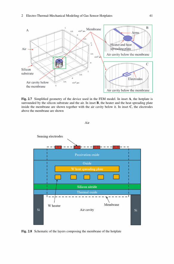
2 Electro-Thermal-Mechanical Modeling of Gas Sensor Hotplates 41
Fig. 2.7 Simplified geometry of the device used in the FEM model. In inset A, the hotplate issurrounded by the silicon substrate and the air. In inset B, the heater and the heat spreading plateinside the membrane are shown together with the air cavity below it. In inset C, the electrodesabove the membrane are shown
Fig. 2.8 Schematic of the layers composing the membrane of the hotplate
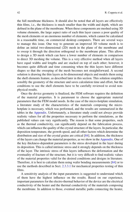
42 R. Coppeta et al.
the full membrane thickness. It should also be noted that all layers are effectivelythin films, i.e., the thickness is much smaller than the width and depth, which aredefined in the plane of the membrane. When these components are meshed using 3Dvolume elements, the large aspect ratio of each thin layer causes a poor quality ofthe mesh elements or an enormous number of elements, which cannot be calculatedin a reasonable time, on commercial desktop computers. There are several waysto manage this issue. One way to generate an improved 3D volume mesh is todefine an initial two-dimensional (2D) mesh in the plane of the membrane andto sweep it through the direction orthogonal to the membrane plane. This allowsto design a 3D mesh which can have a lower number of elements in comparisonto direct 3D meshing the volume. This is a very effective method when all layershave equal widths and lengths and are stacked on top of each other; however, itbecomes quite difficult and time consuming when the thin layers have differentshapes so that the sweeping of the mesh becomes not straightforward. A secondsolution is drawing the thin layers as bi-dimensional objects and models them usingthe shell elements feature, as described later in this section. This solution simplifiessensibly the geometry of the structure and saves calculation time and effort, but theconditions to use the shell elements have to be carefully reviewed to avoid non-physical results.
Once the device geometry is finalized, the FEM software requires the definitionof the material properties. It is paramount to choose the appropriate materialparameters that the FEM model needs. In the case of the micro-hotplate simulation,a literature study of the characteristics of the materials composing the micro-hotplate is necessary, which was performed, and the results are summarized in thetables in the Appendix. Unfortunately, a literature study could not always providerealistic values for all the properties necessary to perform the simulations, as thepublished values can vary significantly. The reason is that some properties, suchas the thermal conductivity, can significantly depend on the fabrication process,which can influence the quality of the crystal structure of the layers. In particular, thedeposition temperature, the growth speed, and all other factors which determine thedistribution and size of the crystal grains are critical [84]. In addition, the thicknessof the layers can change the material properties, as we show in the Appendix. One ofthe key thickness-dependent parameters is the stress developed in the layer duringits deposition. This is called intrinsic stress and it strongly depends on the thicknessof the layer. The intrinsic stress of thin layers influences the deformation and theeventuality of fracture of the structure, but it is very difficult to find realistic valuesof the material properties valid for the desired conditions and designs in literature.Therefore, it is best to calculate them using wafer bending measurements [84] or touse the methods described in Sect. 2.3.3.1 for mechanical properties testing of thinfilms.
A sensitivity analysis of the input parameters is suggested to understand whichof them have the highest influence on the results. Based on our experience,important parameters for the electro-thermal behavior of the device are the electricalconductivity of the heater and the thermal conductivity of the materials composingthe membrane. In addition to those, eventual metallic paths connecting the heater,
2 Electro-Thermal-Mechanical Modeling of Gas Sensor Hotplates 43
or the heater area, to the chip can remove more heat from the active area, therebyincreasing the power consumption; therefore, the properties of the metallic pathsbecome of increased importance.
When the device is biased, its temperature is increased by a value dependenton the applied bias. Many material properties, such as the electrical and thermalconductivity, but also the Young’s modulus, can vary with the temperature, asdiscussed in Sect. 2.3 and shown in the Appendix. Most FEM tools allow for theimplementation of the dependence of the material properties on the temperature.This allows for more realistic results, at the cost of increased simulation time.
Once the geometry and the material properties of the device are defined, it is nec-essary to model the physics of the problem. When the device is biased, an electricalcurrent runs through the circuit, reaching the heater. This is a resistive element andsome power is dissipated due to Joule heating. The material and the shape of theheater are chosen in order to provide the desired amount of power dissipation whileimproving the heat distribution at the desired location, as discussed in more detailin Sect. 2.2.2.1. The Joule heating causes an increase in the temperature, heatingthe sensitive material, which can interact with the gas molecules. The increasingtemperature also has a collateral effect. The material forming the membrane and thesensing layer has different coefficients of thermal expansion (CTEs). This causesmechanical deformation when the device is biased and could lead to fracture if thedesign is not optimized to take this into consideration.
All these considerations lead to the need to model both the electro-thermaland the thermo-mechanical behavior of the device. The procedure is described inthe following. At first, the electrical component is modeled as an AC/DC circuit,depending on the bias applied. Then Joule heating is calculated and transferred tothe thermal model, as defined by the heat equation. The Joule heat is the energysource term which has to be included in the heat equation. Subsequently, the heatequation is solved and the temperature distribution is transferred to the mechanicalmodel of the simulation. In particular, the temperature increase is used to calculatethe deformation caused by the difference of the CTEs. This forces the membraneto bend with respect to the original position. Finally, Hooke’s law relates thisdeformation to the stress distribution inside the device. The possibility of fracturecaused by the stress and the methods to limit it are discussed in Sect. 2.5.2.
The first step to model the electrical behavior is to set the terminals which definethe difference in potential across the circuit. Based on our experience, it is notnecessary to draw and model the entire electric circuit but only the part embeddedinto the membrane. In relation to Fig. 2.7, this is the heater with the two arms,depicted in inset B. Subsequently, the extremities are set as the terminals of thecircuit, where the bias is applied. The circuit can be modeled using simple threedimensional elements if the thickness of the heater has comparable dimensionswith the width and the depth. If not, the meshing operations could be difficult andproduce elements with a poor quality. Consequently, it is necessary to refine themesh by increasing the number of elements, which increases the simulation time.To overcome this issue, it is faster to draw each thin layer as a shell element definingits thickness in the shell interface. This may reduce the accuracy of the simulation,

44 R. Coppeta et al.
but only minimally, considering that the normal component plays almost no role ina thin film’s behavior. When a DC bias is applied, the electric behavior is describedby
∇ · −→j = Qj,V , (2.18)
−→j = σ
−→E , (2.19)
and
−→E = −∇V, (2.20)
where−→j is the current density, Qj,V is the current source, σ is the electrical
conductivity,−→E is the electric field, and V is the applied potential. When the shell
element is used, the equations are modified to use the tangential gradient operator,which removes the normal component from the gradient operation, so that onlytangential components remain. This is mathematically expressed for the potentialfield V as
∇−→T
V = ∇V − (∇V · −→n) · −→
n . (2.21)
Thus, the normal gradient operator is
∇−→N
V = (∇V · −→n) · −→
n . (2.22)
In case a shell element is used, the equations are modified as
∇−→T
·(ds
−→j)
= dsQj,V (2.23)
and
−→E = −∇−→
TV, (2.24)
where the subscript s denotes the layer and ds is the thickness of the layer.After the electrical behavior is modeled, it is necessary to describe the thermal
problem using the heat equation, which is defined over the entire structure in thestationary case as
∇ · (k∇T ) = −Qj, (2.25)
where
Qj = −→j · −→
E . (2.26)
2 Electro-Thermal-Mechanical Modeling of Gas Sensor Hotplates 45
Here, T is the temperature, k is the thermal conductivity, Qj is the Joule heat, andthe heat flux is represented by
−→q = −k∇T . (2.27)
The layers, which are much thinner compared to the total thickness of themembrane, can be drawn and modeled as bi-dimensional elements. The boundaryconditions of these thin layers require the definition of their real thickness. If athin layer is a bad thermal conductor compared to adjacent elements, the tangentialheat flux can be neglected and only the heat flux across the layer’s thickness isconsidered. When the thin layer is instead a good thermal conductor, the temperaturedifference and the heat flux across the layer’s thickness are neglected and only thetangential flux is considered. In our simulations, the general case, where both thetangential and normal heat fluxes are considered in the calculation, is assumed:
∇−→T
· −→qs = Qs (2.28)
−→qs = −ks
(∇−→
TTs + ∇−→
NTs
)(2.29)
Here, Qs is the Joule heat and −→qs is the heat flux in the layer.
The heat equation as presented before includes the conduction, but not theconvection of the heat, which could take place in the air. In the simulated cases,the convection has a negligible impact on the results; therefore, it is not included inthe FEM model. A deeper discussion on the sources of heat loss is given in Sect.2.2.2.2.
Once the mathematical equations describing the electro-thermal behavior ofthe device are defined, it is necessary to choose appropriate boundary conditions(BCs) to ensure realistic results. Appropriate BCs have to be assigned also to thephysical boundaries of the FEM model. In fact, it is not possible to include theentire electronic circuit around the sensor in the FEM model as it would require anunmanageable computational cost. Therefore, it is necessary to exclude it and assignappropriate BCs to the extents of the model.
In our simulations, a good match between the FEM results and the experimentaldata is obtained when the hotplate is surrounded by a thick layer of silicon. Thereason is that, in reality, the hotplate is connected to the heat source through thearms and is isolated by the silicon from other metallic paths. Therefore, there are noother metal interconnections which could cause heat losses to the system.
The external surfaces of the silicon domain are assumed to be thermal insulators,i.e., the heat flux through them is zero. Our simulations show that this conditionensures realistic results of the FEM simulation if the distance between the sensor andthe external surfaces of the silicon domain is at least double the membrane diameterof the gas sensor. This implies that the system can dissipate the heat only through the
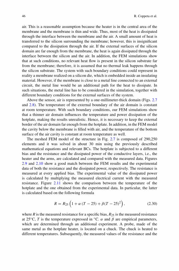
46 R. Coppeta et al.
air. This is a reasonable assumption because the heater is in the central area of themembrane and the membrane is thin and wide. Thus, most of the heat is dissipatedthrough the interface between the membrane and the air. A small amount of heat istransferred to the silicon surrounding the membrane; however, this is insignificantcompared to the dissipation through the air. If the external surfaces of the silicondomain are far enough from the membrane, the heat is again dissipated through theinterface between the silicon and the air. In addition, the FEM simulations showthat at such conditions, no relevant heat flow is present in the silicon substrate farfrom the membrane; therefore, it is assumed that no thermal leak happens throughthe silicon substrate. The system with such boundary conditions could represent inreality a membrane realized on a silicon die, which is embedded inside an insulatingmaterial. However, if the membrane is close to a metal line connected to an externalcircuit, the metal line would be an additional path for the heat to dissipate. Insuch situations, the metal line has to be considered in the simulation, together withdifferent boundary conditions for the external surfaces of the system.
Above the sensor, air is represented by a one-millimeter-thick domain (Figs. 2.7and 2.8). The temperature of the external boundary of the air domain is constantat room temperature. With such boundary conditions, our FEM simulations showthat a thinner air domain influences the temperature and power dissipation of thehotplate, making the results unrealistic. Hence, it is necessary to keep the externalborder of the air domain far enough from the hotplate. In addition, in the FEM modelthe cavity below the membrane is filled with air, and the temperature of the bottomsurface of the air cavity is constant at room temperature as well.
The meshed FEM model of the structure in Fig. 2.7 is composed of 290,250elements and it was solved in about 30 min using the previously describedmathematical equations and relevant BCs. The hotplate is subjected to a differentbias and the resistance and the dissipated power of the conductive layers, i.e., theheater and the arms, are calculated and compared with the measured data. Figures2.9 and 2.10 show a good match between the FEM results and the experimentaldata of both the resistance and the dissipated power, respectively. The resistance ismeasured at every applied bias. The experimental value of the dissipated poweris calculated by multiplying the measured electrical current with the measuredresistance. Figure 2.11 shows the comparison between the temperature of thehotplate and the one obtained from the experimental data. In particular, the latteris calculated based on the following formula
R = R25
(1 + α (T − 25) + β(T − 25)2
), (2.30)
where R is the measured resistance for a specific bias, R25 is the measured resistanceat 25◦C, T is the temperature expressed in ◦C. α and β are empirical parameters,which are determined through an additional experiment. A probe, made of thesame metal as the hotplate heater, is located on a chuck. The chuck is heated todifferent temperatures. Subsequently, the measured values of the resistance and the
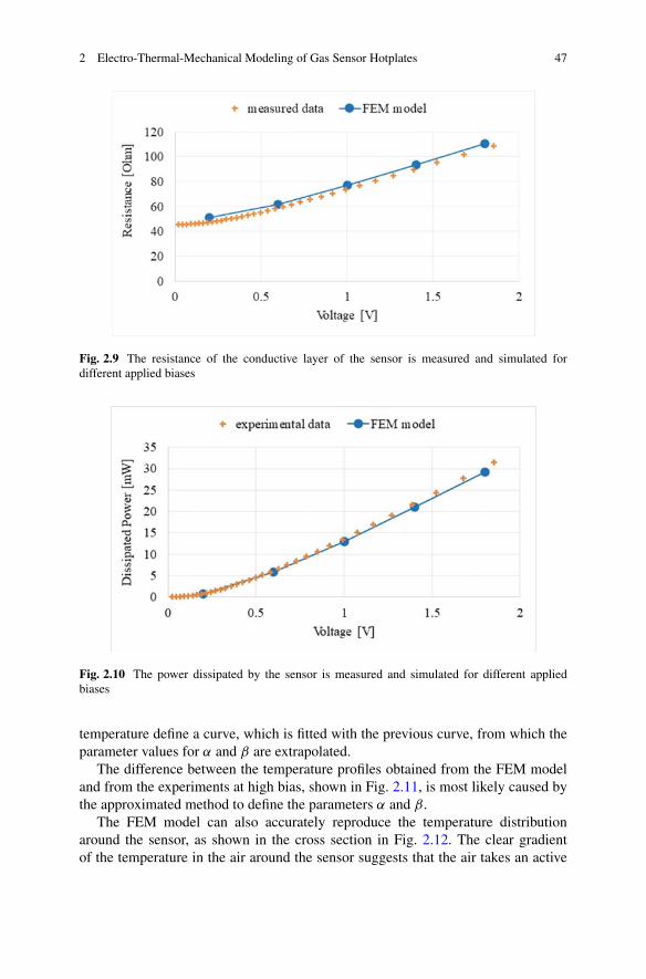
2 Electro-Thermal-Mechanical Modeling of Gas Sensor Hotplates 47
Fig. 2.9 The resistance of the conductive layer of the sensor is measured and simulated fordifferent applied biases
Fig. 2.10 The power dissipated by the sensor is measured and simulated for different appliedbiases
temperature define a curve, which is fitted with the previous curve, from which theparameter values for α and β are extrapolated.
The difference between the temperature profiles obtained from the FEM modeland from the experiments at high bias, shown in Fig. 2.11, is most likely caused bythe approximated method to define the parameters α and β.
The FEM model can also accurately reproduce the temperature distributionaround the sensor, as shown in the cross section in Fig. 2.12. The clear gradientof the temperature in the air around the sensor suggests that the air takes an active
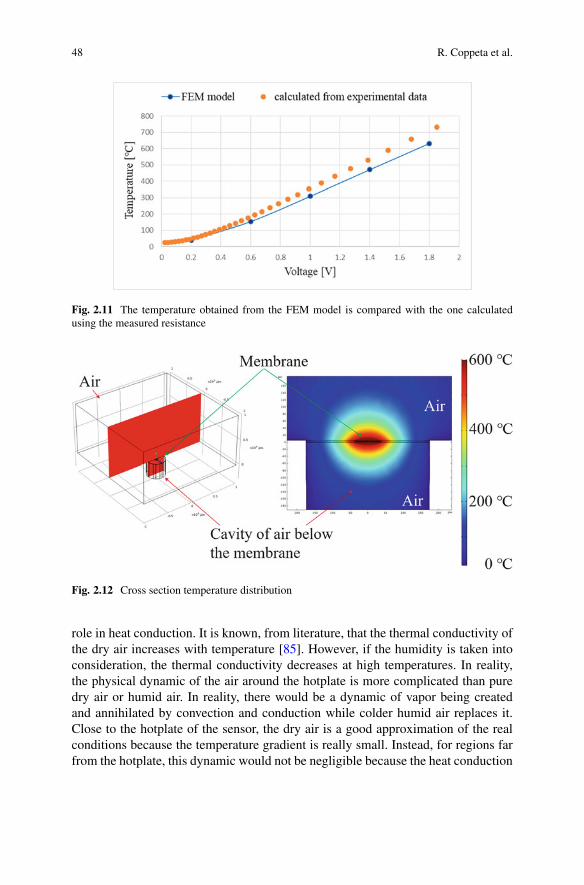
48 R. Coppeta et al.
Fig. 2.11 The temperature obtained from the FEM model is compared with the one calculatedusing the measured resistance
Fig. 2.12 Cross section temperature distribution
role in heat conduction. It is known, from literature, that the thermal conductivity ofthe dry air increases with temperature [85]. However, if the humidity is taken intoconsideration, the thermal conductivity decreases at high temperatures. In reality,the physical dynamic of the air around the hotplate is more complicated than puredry air or humid air. In reality, there would be a dynamic of vapor being createdand annihilated by convection and conduction while colder humid air replaces it.Close to the hotplate of the sensor, the dry air is a good approximation of the realconditions because the temperature gradient is really small. Instead, for regions farfrom the hotplate, this dynamic would not be negligible because the heat conduction
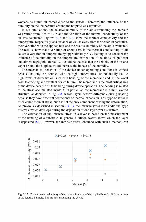
2 Electro-Thermal-Mechanical Modeling of Gas Sensor Hotplates 49
worsens as humid air comes close to the sensor. Therefore, the influence of thehumidity on the temperature around the hotplate was simulated.
In our simulations, the relative humidity of the air surrounding the hotplatewas varied from 0.25 to 0.75 and the variation of the thermal conductivity of theair was calculated. Figures 2.13 and 2.14 show the thermal conductivity and thetemperature, respectively, at a distance of 75 μm away from the heater. In particular,their variation with the applied bias and the relative humidity of the air is evaluated.The results show that a variation of about 15% in the thermal conductivity of aircauses a variation in temperature by approximately 5◦C, leading us to consider theinfluence of the humidity on the temperature distribution of the air as insignificantand almost negligible. In reality, it could be the case that the velocity of the air andvapor around the hotplate would increase the impact of the humidity.
The mechanical behavior of the device under operating conditions is criticalbecause the long use, coupled with the high temperatures, can potentially lead tohigh levels of deformation, such as a bending of the membrane and, in the worstcase, to cracking and eventual device failure. The membrane is the most critical areaof the device because of its bending during device operation. The bending is relatedto the stress accumulated inside it. In particular, the membrane is a multilayeredstructure, as depicted in Fig. 2.8, whose layers deform differently during heatingbecause they have different coefficients of thermal expansion. This type of stress isoften called thermal stress, but it is not the only component causing the deformation.As previously described in section 2.3.3.3, the intrinsic stress is an additional typeof stress, which develops during the deposition of one layer over a substrate.
The estimation of the intrinsic stress in a layer is based on the measurementof the bending of a substrate, in general a silicon wafer, above which the layeris deposited [84]. However, the intrinsic stress, obtained with such a method, can
Fig. 2.13 The thermal conductivity of the air as a function of the applied bias for different valuesof the relative humidity f of the air surrounding the device
50 R. Coppeta et al.
Fig. 2.14 The temperature of the air as a function of the applied bias for different values of therelative humidity f of the air surrounding the device
differ significantly from the one in a layer with a different and complex shape andembedded inside an insulating material; this is the case for the heater embedded insilicon oxide (Figs. 2.7 and 2.8). In such conditions, the measurement of the intrinsicstress is difficult and, in order to ensure accurate simulations, it is necessary tocalibrate its value in the FEM model with the measured out-of-plane displacement ofthe unbiased hotplate membrane. The calibration procedure is quite straightforwardwhen the geometry of the structure is simple, but it could become cumbersome andnear-impossible when the interfaces among the layers are many and have complexshapes. The intrinsic stresses are added to the FEM model as a boundary condition.
The out-of-plane displacement of a hotplate membrane, similar to the onedepicted in Fig. 2.7, along the diameter of the membrane top surface at roomtemperature was measured with a profilometer prior to applying any bias. Themeasured profile showed that the membrane bends downward by ∼100 nm.Simulations of the mechanical behavior of the membrane prior to any bias beingapplied were performed using measured values of the intrinsic stress for the siliconoxide 280 MPa, the silicon nitride −260 MPa, and for the tungsten 1330 MPa.These values are obtained by measuring wafer bending above which a thin layer oftungsten, oxide, or silicon nitride was deposited [85]. The results of the FEM modelprior to any bias (Fig. 2.15) provide a membrane bending with the same order ofmagnitude of the measured profile. Eventual discrepancies could be caused by thefact that there is some variation in the real intrinsic stresses, which could be differentfrom the calibrated ones used in the simulation.
Once the calibration is complete, the operating conditions are simulated byapplying a bias to the device. The stress and the deformation of the membraneare subsequently calculated with the following hypothesis: All materials composingthe structure are assumed to behave linearly elastic. Eventual plastic deformation or
2 Electro-Thermal-Mechanical Modeling of Gas Sensor Hotplates 51
Fig. 2.15 FEM model results of the out-of-plane displacement of the top surface of the membranealong its radius of the membrane. The hotplate is biased and the deformation is caused by theintrinsic and the thermal stress caused by the temperature increase due to the Joule effect. Zerodisplacement indicates the un-deformed state of the hotplate
creep phenomena of the heater and the other metallic layers inside the membrane arenegligible when they are made of tungsten. In fact, we performed some experimentsof temperature-driven stress relaxation of polycrystalline tungsten films, depositedon a silicon wafer, close to the tungsten deposition temperature. The resultsshow that the creep and the consequent stress relaxation are negligible in thefirst 5 h of experimental observation. Afterwards, these two phenomena are nolonger negligible. When the heater of the micro-hotplate is made of polycrystallinesilicon, no plastic deformation or creep behavior are expected with normal operatingconditions. Therefore, in our devices, both creep and plasticity are neglected on thebasis of the experimental observations and the linear elasticity theory is used in theFEM model, as described below.
The Joule heating causes the deformation of the structure because it is composedof materials having different coefficients of thermal expansions. In particular theelastic strain of a layer, with the CTE α, caused by heating ΔT is
εth = α · T (2.31)
Assuming that the materials behave linearly elastic, they are described by Hooke’slaw, which relates the elastic strain εel and the stress S as
S = S0 + C : εth, (2.32)

52 R. Coppeta et al.
where C is the stiffness tensor, which depends on the Young’s modulus and thePoisson ratio only in the case of an isotropic body and S0 is the intrinsic stress ofthe layer. In a notation where the indices are shown, the same equation would read
σij = S0,ij +3∑
k=1
3∑
l=1
cijklεkl . (2.33)
The displacements are calculated as
εth = 1
2
[(∇−→u)T + ∇−→
u], (2.34)
where −→u is the displacement vector. In case the thin layers are modeled using shell
elements, the equation is slightly modified as
εth = 1
2
(∇t−→u). (2.35)
One boundary condition of the mechanical model is that the bottom surface ofthe silicon domain (Fig. 2.7) is physically fixed, i.e., the displacements in the threeorthogonal directions are zero. In addition, the intrinsic stress of each layer could beneglected, as a result of the calibration. If the device is not directly subjected to anyexternally applied loads, the intrinsic and thermal stresses are the only stress typesconsidered in the FEM model.
Considering the hotplate membrane shown in Figs. 2.7 and 2.8, thin layers (i.e.,the heater, the heat spreading plate, and silicon nitride) are simulated using shellelements in our FEM model. Using the equations of the mechanical behavior, cou-pled with the electro-thermal model described previously, the simulation providesthe profile of the membrane displacement on its out-of-plane direction for differentapplied biases (see Fig. 2.15).
In general, the membrane bends downward at 0 V as a result of the relaxation ofthe intrinsic stress. The center of the membrane, which contains the W heater andheat spreading plate, has an upward displacement of about 100 nm.
Increasing the applied bias up to 1.8 V, the displacement of the central areaincreases from −100 nm to 200 nm as a result of the Joule effect. Since the heatingconcerns more the central area of the membrane, as it contains the heater, thesections of the membrane far from the center are less displaced.
The results show another interesting effect of Joule heating. At room temperature,i.e., when no bias is applied, the maximum principal stress along the heater and thearms is approximately equal to the intrinsic one, inserted as a boundary condition.Increasing the bias, i.e., the temperature, the stress in the W heater decreases. Thishappens because the W heater has a higher CTE with respect to the oxide, thus theheater expansion is limited by the oxide and a compressive stress is created and itcompensates the initial high tensile stress. The consequence is that the total stress isgradually reduced by increasing the bias, i.e., increasing the temperature.
2 Electro-Thermal-Mechanical Modeling of Gas Sensor Hotplates 53
Fig. 2.16 FEM model resultsof the maximum principalstress along the arms of theheater
Despite this, Fig. 2.16 shows that the stress in the arms remains high at highbias, instead of decreasing. This happens because the Joule effect is weaker in thearms than in the heater, thus no compressive stress is created during the heating.During the operating lifetime of the hotplate, the device is continously switched onand off, but this does not reduce the stress in the arms; therefore, the arms couldbe subjected to damage deriving from cycling fatigue. These phenomena deservemore experimental investigations in order to be proven and a more sophisticatedmechanical model should be developed.
2.5 Fracture Modeling for Mechanical Robustness of SensorComponents
Thermo-electrical characterization and modeling of components for microelectronicapplications, such as gas sensor hotplates, are very well established in the researchactivities of the microelectronic industry. With the progress towards new materialsand complex designs, the need for mechanical stability of the components isincreasing. The reliability of thin film stacks can be improved if the materialproperties and internal mechanical loading conditions are properly utilized. Initialdefects, due to manufacturing, cannot be excluded and for that reason a deviceshould be designed in order to be failure tolerant. The two major questions whichhave to be addressed are: Is there a fracture parameter that can properly describecrack propagation in such systems and how can we determine the crack drivingforce in thin film stacks.
54 R. Coppeta et al.
2.5.1 Residual Stresses in Thin Films for Gas Sensor Hotplates
Special attention has to be paid to the role of residual stresses on failure processesand their influence on the reliability and functionality of components [84, 86].Residual stresses in thin films used in microelectronic components, such as gassensor hotplates, can reach very high values, i.e., in the order of GPa [87–90]. Evenif the average residual stress within the layer or in layer stacks does not seem to becritical, strong stress gradients can appear [89, 90]. The local residual stress valuescan even exceed the tensile, compressive or shear strength and interface strengths ofthe materials, leading to cracking and delamination within the component [91]. Ingeneral, residual stress is composed of intrinsic stress, formed during deposition,and extrinsic (thermal) stress stemming from the mismatch in the coefficient ofthermal expansion between the individual layers and the substrate [84], as discussedin Sect. 2.3.3.
Two groups of methods, which enable local and depth resolved residual stresscharacterization have evolved over the last years. Within the first group we find X-ray methods performed in grazing incidence or in transmission. Recent developmentof the latter uses focused synchrotron X-ray beams [92–95]. The second groupincludes methods where a specific region with characteristic features is imagedbefore and after local removal of a stressed material using, for example, ion beammilling. The form of the processed area can have numerous geometrical shapes [70,71]. This results in a local relief of residual stress and a consequential deformationof the sample, from which the strains and stresses can be reconstructed analyticallyor using finite element modeling, when the stiffness is known [72, 73, 96, 97]. Incontrast to the X-ray methods, these methods work without the need for the presenceof crystalline phases and can also be applied to amorphous materials.
In many applications, small amounts of residual stresses are tolerable and do nothave a significant influence on the performance or reliability of a device. On theother hand, residual stresses have been shown to have decisive impact on the crackdriving force in a material when high enough. While tensile residual stresses, ingeneral, increase the crack driving force, compressive residual stresses are desiredbecause of their crack stopping capabilities. In the case of compressive residualstress, however, the risk for delamination increases [84]. Thus, in order to increasethe reliability of microelectronic components in general, and gas sensor hotplates inparticular, it is of uttermost importance to work on increasing the failure resistanceof the components on the one hand (e.g., layer design for fracture toughness,interface strength) and the reduction of failure driving forces (e.g., CTE mismatchesand intrinsic residual stress engineering) on the other.

2 Electro-Thermal-Mechanical Modeling of Gas Sensor Hotplates 55
2.5.2 Fracture Mechanics for Thin Films inGas Sensor Hotplates
The topic of fracture mechanics is one of the most active fields of research and wasalready extensively investigated in the past. The basics of fracture mechanics arecollected in different books and publications [98, 99]. The book by Kolednik [100]gives a very good overview of fracture mechanics. In the course of this section, themost relevant concepts and terms of fracture mechanics are introduced, along withhow fracture mechanics applies to thin film structures for sensing applications.
2.5.2.1 Definition of the Crack Driving Force
Imagine a homogeneous body with an initial crack under loading, as shown inFig. 2.17. Generally, this crack with an initial length a0 will extend if the crackdriving force (CDF) D equals or exceeds the crack growth resistance R [100,101]. The CDF D describes a loading parameter deduced from the strain energyand the work from external loading. The crack growth resistance R will preventcrack propagation. It depends on the fracture toughness of the material, on thecrack extension a (because of the increasing size of the plastic zone) and on thegeometry (because of the constraint effect), shown in Fig. 2.17. If D < R, the crackwill remain stationary. However, if D = R, the crack will exhibit stable growth, andif D > R, crack growth becomes unstable.
Fig. 2.17 A homogeneousbody under Mode I loading.The initial crack length is a0and the current crack length isdenoted by α and togetherwith the ligament length b itgives the specimenthickness W

56 R. Coppeta et al.
2.5.2.2 Regimes of Fracture Mechanics
In a simple distinction, fracture mechanics can be divided into linear elastic fracturemechanics (LEFM) and elastic–plastic or nonlinear fracture mechanics (E–PFM,NLFM) [100]. The concept of LEFM applies if the plastic deformation during crackgrowth is zero or limited. In this case, the size of the plastic zone rpl is very smallcompared to the crack length a and the ligament length b, rpl a, b, in which casesmall-scale yielding (ssy) conditions apply, shown in Fig. 2.18a.
E–PFM, on the other hand, is used if the body experiences significant plasticdeformation. In a homogeneous body with a long crack, the prevailing conditionsare either large-scale yielding (lsy) or general yielding (gy), as shown in Fig. 2.18b.Under the lsy conditions, the onset of plastic deformation is at the back face ofthe body, while gy applies when the crack tip plastic zone and back face plasticitymerge into one plastic zone. In a special case where the crack is very short, asshown in Fig. 2.18c, E–PFM has to be applied, since also a small plastic zone doesnot comply with the conditions from Fig. 2.18a. In layered composites, such as thinmetallic film stacks shown in Fig. 2.18c, the materials deform in a different way andoften the lsy condition cannot be defined by the onset of back face plasticity. In thiscase, lsy applies if the size of the plastic zone rpl compares to or is higher than thecrack length a.
2.5.2.3 Linear Elastic Fracture Mechanics
The stresses close to the crack tip of a linear elastic body are calculated by [102]
σij = K√2πr
fij (θ) , (2.36)
with the polar coordinates (r, θ ), the angular stress functions fij(θ ) and
K = σap√
πafK. (2.37)
K describes the intensity of the near-tip stress field and is therefore called thestress intensity factor. It depends on the applied stress σ ap, the crack length a, andthe geometry of the body, represented by fK . However, the equation for the near-tipstresses implies a singular behavior of the stress field, as r → 0, which is not thecase in reality. Plastic deformation generated at the crack tip keeps the stresses finite,but for as long as the plastic zone is reasonably small the stress intensity factor Kis a valid measure for the CDF. Moreover, as the stresses or strains at the crack tipequal or exceed a critical value K = KC, fracture occurs. The material parameterKC is called fracture toughness and describes the resistance of the material againstfracture. Connecting this stress and strain deformation concept to the energy-basedperspective of a CDF D, one finds the relation
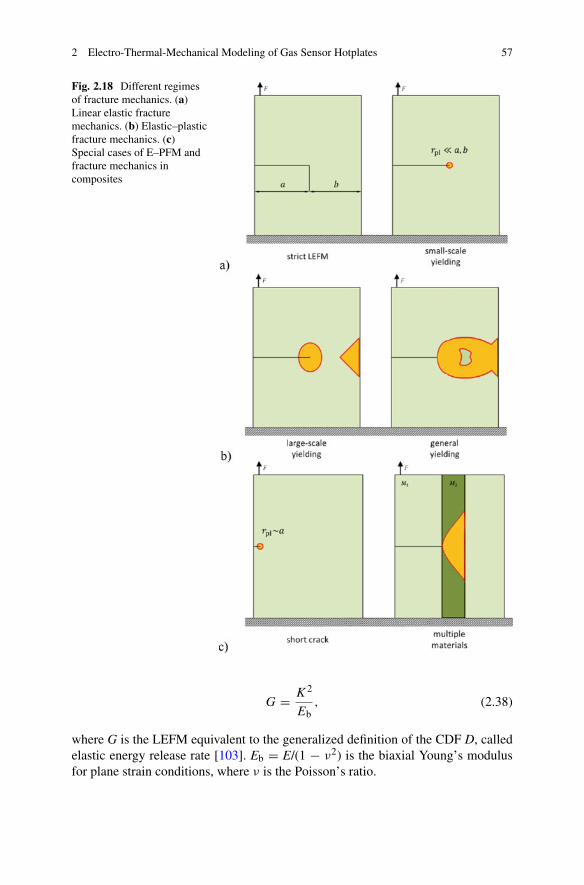
2 Electro-Thermal-Mechanical Modeling of Gas Sensor Hotplates 57
Fig. 2.18 Different regimesof fracture mechanics. (a)Linear elastic fracturemechanics. (b) Elastic–plasticfracture mechanics. (c)Special cases of E–PFM andfracture mechanics incomposites
G = K2
Eb, (2.38)
where G is the LEFM equivalent to the generalized definition of the CDF D, calledelastic energy release rate [103]. Eb = E/(1 − ν2) is the biaxial Young’s modulusfor plane strain conditions, where ν is the Poisson’s ratio.
58 R. Coppeta et al.
2.5.2.4 Nonlinear and Elastic–Plastic Fracture Mechanics
In the regime where plastic deformation becomes relevant, the concept of LEFMwill fail. The stress intensity factor K has to be extended into a parameter valid forNLFM and E–PFM. Based on the deformation theory of plasticity from 1968, afracture parameter called J-integral was introduced by Rice [104]. Similar to K, theJ-integral describes the intensity of the near-tip stress field and crack growth occursif the corresponding critical value is reached. The J-integral describes a contourintegral on an arbitrary path around the crack tip. It was shown by Rice [99] that theJ-integral is the equivalent to the energy release rate of work done on a nonlinearelastic body containing a crack per unit fracture area. This can be understood asa more generalized version of the elastic energy release rate G. For LEFM, the J-integral is identical to G; consequently, a relationship between the stress intensityfactor K and the J-integral can be established:
Jel = K2
Eb(2.39)
There are some limitations concerning the conventional J-integral proposed byRice when applying it to real elastic–plastic materials, pointed out by Simha etal. [105] and Kolednik et al. [106]. The conventional J-integral is based on thetheory of plastic deformation, assuming nonlinear elastic behavior for elastic–plasticmaterials. In a real elastic–plastic material, for example, the unloading portion ofthe stress–strain curve is not following the loading curve, as is the case in NLFM.The material unloads linear elastically, depending on the elastic properties of thematerial. Thus, the total strain energy density can be split into an elastic and plasticpart. The plastic strain energy density is absorbed for plastic deformation in front ofthe crack tip and the elastic part of the total strain energy density is available to drivecrack extension. For a proper description for elastic–plastic materials incrementaltheory of plasticity is necessary. In this case, the NLFM J-integral does not directlydescribe a CDF for real elastic–plastic materials. It acts as a measure of the intensityof the crack tip stress field, comparable to the stress intensity factor K in LEFM.
Gas sensor hotplates, for example, are constantly subjected to nonproportionalloading conditions in operation. Additionally, several inhomogeneities have adistinct influence on the failure behavior in the thin film systems, and render thedetermination of critical fracture parameters and critical loading conditions difficult.
2.5.2.5 Configurational Force Concept and the J-Integral
Material imperfections, smooth or discontinuous material variations, as well asresidual stresses, are known to have an influence on the CDF in a body [106–114].A very convenient way to describe the impact of material inhomogeneities on thefracture behavior is provided by the configurational force concept, which is basedon the ideas of Eshelby [115], and adopted by Gurtin [116] and Maugin [117].

2 Electro-Thermal-Mechanical Modeling of Gas Sensor Hotplates 59
This concept makes it theoretically possible to describe any kind of inhomogeneousbehavior in a body. Examples for inhomogeneities or imperfections in a material arecracks, voids, dislocations, and sharp interfaces.
In the following, the basic idea of the configurational force concept is given. Forcomprehensive derivations of the following equations and definitions, the reader isreferred to [106, 108, 115–117].
From a thermodynamical point of view, a configurational force (CF) tries to pusha defect into a configuration where the total potential energy of the system has itsminimum. In general, a CF vector f can be calculated at each material point ina body. It is defined as the divergence of the configurational stress tensor C andbecomes non-zero only at positions of a defect in the body
f = −∇ · C = −∇ ·(φI − FTS
), (2.40)
where φ is the Helmholtz-free energy or strain energy density, I represents theidentity tensor, and FT and S are the transposed deformation gradient and the firstPiola–Kirchhoff stress tensor, respectively [106, 108].
If, for example, a two-dimensional homogeneous elastic body with a sharp crackis considered, the crack tip exhibits a CF vector ftip, determined by
ftip = − limr→0
∫
�r
(φI − FTS
)mdl. (2.41)
Here, �r is the contour around the crack tip at the distance r away from the cracktip and m denotes the unit normal vector to the contour. The corresponding energydissipated per unit crack extension is a projection of ftip in the direction of crackextension e and gives
Jtip = −e · ftip, (2.42)
where Jtip is the scalar near-tip J-integral and it represents the CDF. If the bodyis externally loaded the CDF is equal to Jtip = Jfar, where Jfar is the far-field J-integral, which can be understood as the driving force induced by the external loadin the body.
2.5.2.6 Material Inhomogeneity Term
Suppose we have a layer stack where two materials M1 and M2, as shown inFig. 2.19, are separated by a sharp interface (IF) �. The material properties, such asthe Young’s modulus, experience a jump and, therefore, CFs f� are induced at thesharp IF, shown in Fig. 2.19, given by [118]:
f� = −(�φ� I −
�FT
�〈S〉)
n (2.43)
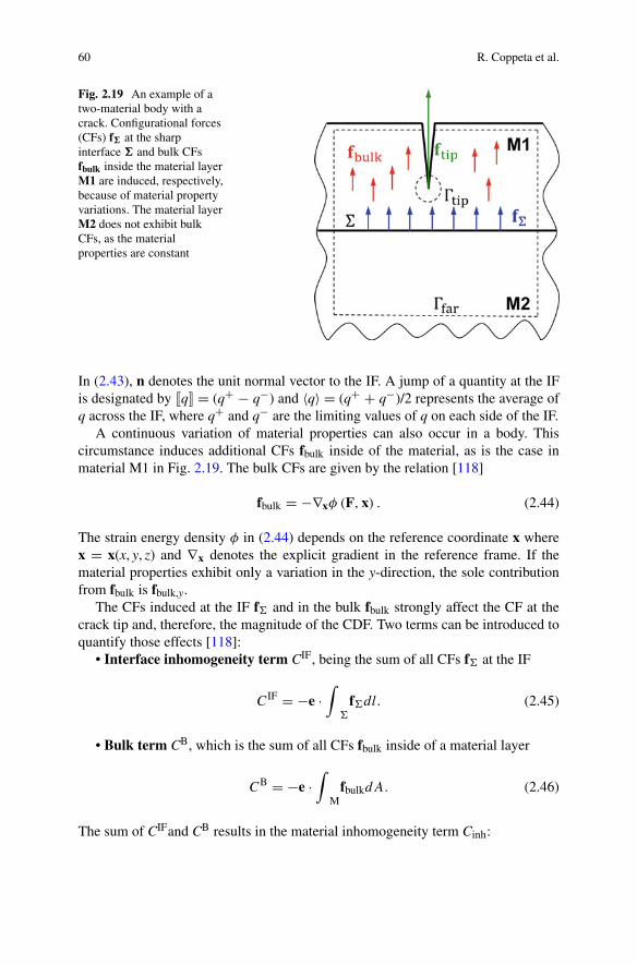
60 R. Coppeta et al.
Fig. 2.19 An example of atwo-material body with acrack. Configurational forces(CFs) f� at the sharpinterface � and bulk CFsfbulk inside the material layerM1 are induced, respectively,because of material propertyvariations. The material layerM2 does not exhibit bulkCFs, as the materialproperties are constant
In (2.43), n denotes the unit normal vector to the IF. A jump of a quantity at the IFis designated by �q� = (q+ − q−) and 〈q〉 = (q+ + q−)/2 represents the average ofq across the IF, where q+ and q− are the limiting values of q on each side of the IF.
A continuous variation of material properties can also occur in a body. Thiscircumstance induces additional CFs fbulk inside of the material, as is the case inmaterial M1 in Fig. 2.19. The bulk CFs are given by the relation [118]
fbulk = −∇xφ (F, x) . (2.44)
The strain energy density φ in (2.44) depends on the reference coordinate x wherex = x(x, y, z) and ∇x denotes the explicit gradient in the reference frame. If thematerial properties exhibit only a variation in the y-direction, the sole contributionfrom fbulk is fbulk,y.
The CFs induced at the IF f� and in the bulk fbulk strongly affect the CF at thecrack tip and, therefore, the magnitude of the CDF. Two terms can be introduced toquantify those effects [118]:
• Interface inhomogeneity term CIF, being the sum of all CFs f� at the IF
CIF = −e ·∫
�
f�dl. (2.45)
• Bulk term CB, which is the sum of all CFs fbulk inside of a material layer
CB = −e ·∫
MfbulkdA. (2.46)
The sum of CIFand CB results in the material inhomogeneity term Cinh:
2 Electro-Thermal-Mechanical Modeling of Gas Sensor Hotplates 61
Cinh = CIF + CB (2.47)
The balance of CFs is therefore fulfilled if the material inhomogeneity term Cinh isintroduced, which renders the CDF to be [108, 118]
Jtip = Jfar + Cinh, (2.48)
where Jfar is calculated around the far-field contour �far as shown in Fig. 2.19. Inthis context, Cinh corresponds to the CDF caused by the material inhomogeneitiesat a given loading Jfar in the body. An anti-shielding effect is described by a positiveshielding by a negative value of Cinh.
In the same way, a material inhomogeneity effect is induced if, instead of thematerial properties, the eigenstrains or the resulting eigenstresses that exhibit a jumpor smooth variation [114, 118].
2.5.3 Crack Driving Force in Thin Film Stacks forMicro-Hotplates
In the following, some results for an application of the introduced fracture mechan-ics concept are presented. The CDF is determined numerically for a tri-layer stack,where a 0.3 μm thin tungsten (W) heater-layer is sandwiched between two 1.5 μmthick silicon dioxide (SiO2) layers, and positioned on a 5.0 μm thick silicon (Si)substrate, as shown in Fig. 2.20. After performing fracture simulations on a micro-cantilever beam [119], the CDF can be calculated by applying Eqs. (2.43)–(2.48).
Linear elastic and elastic–plastic simulations are performed where tensile resid-ual stresses for SiO2 and W are considered as internal loading, denoted by LERSand EPRS, respectively, depicted in Fig. 2.21a.
The material properties used for modeling are given in Table 2.2. Note that aftera crack is introduced into the system, the residual stresses have to redistribute inorder to reach an equilibrium state, causing a finite CDF value. The influence of theYoung’s modulus and yield strength inhomogeneity on the CDF is demonstratedfor an increasing crack length. For a better understanding, it has to be mentionedthat in a homogeneous linear elastic material the CDF, in form of the J-integral,would increase linearly for an increasing crack length while under the same load.Additionally, the upper and lower dashed lines represent critical J-integral values JCfor W and SiO2, respectively, calculated from literature fracture toughness values[120, 121].
As the crack transitions from the compliant SiO2 layer to the stiffer W layer, seeTable 2.2, the CDF is reduced by the shielding effect from the Young’s modulusinhomogeneity at the first IF. When elastic–plastic properties are considered theyield strength inhomogeneity causes a slight increase of Jtip very close to thefirst IF compared to the LERS calculation, which was expected as SiO2 behaves
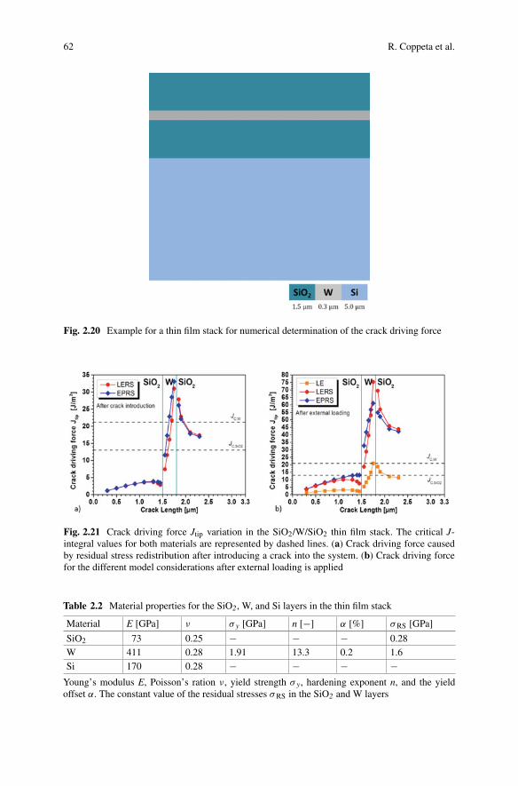
62 R. Coppeta et al.
Fig. 2.20 Example for a thin film stack for numerical determination of the crack driving force
Fig. 2.21 Crack driving force Jtip variation in the SiO2/W/SiO2 thin film stack. The critical J-integral values for both materials are represented by dashed lines. (a) Crack driving force causedby residual stress redistribution after introducing a crack into the system. (b) Crack driving forcefor the different model considerations after external loading is applied
Table 2.2 Material properties for the SiO2, W, and Si layers in the thin film stack
Material E [GPa] ν σ y [GPa] n [−] α [%] σRS [GPa]
SiO2 73 0.25 − − − 0.28W 411 0.28 1.91 13.3 0.2 1.6Si 170 0.28 − − − −
Young’s modulus E, Poisson’s ration ν, yield strength σ y, hardening exponent n, and the yieldoffset α. The constant value of the residual stresses σRS in the SiO2 and W layers
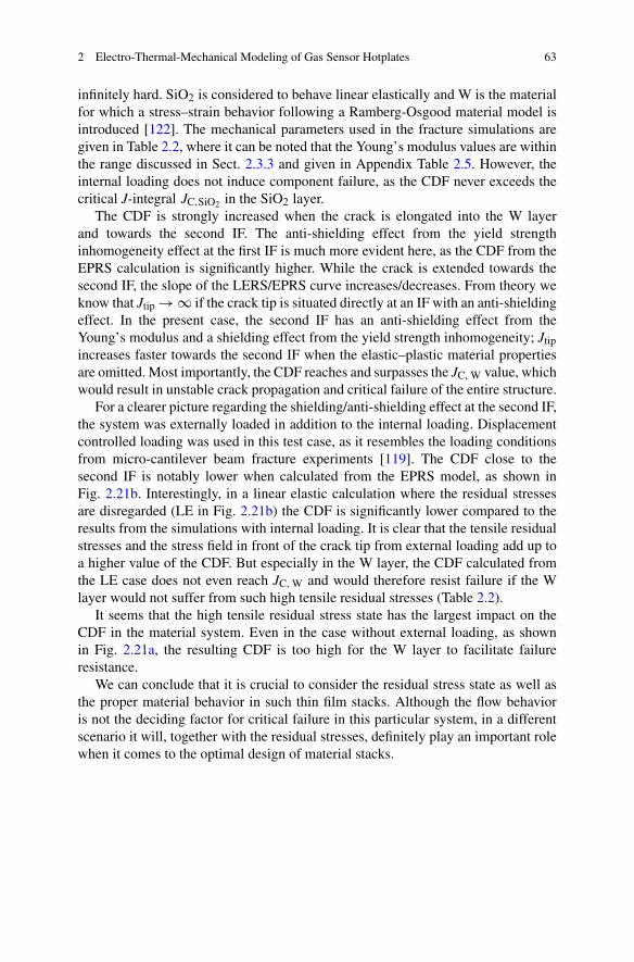
2 Electro-Thermal-Mechanical Modeling of Gas Sensor Hotplates 63
infinitely hard. SiO2 is considered to behave linear elastically and W is the materialfor which a stress–strain behavior following a Ramberg-Osgood material model isintroduced [122]. The mechanical parameters used in the fracture simulations aregiven in Table 2.2, where it can be noted that the Young’s modulus values are withinthe range discussed in Sect. 2.3.3 and given in Appendix Table 2.5. However, theinternal loading does not induce component failure, as the CDF never exceeds thecritical J-integral JC,SiO2 in the SiO2 layer.
The CDF is strongly increased when the crack is elongated into the W layerand towards the second IF. The anti-shielding effect from the yield strengthinhomogeneity effect at the first IF is much more evident here, as the CDF from theEPRS calculation is significantly higher. While the crack is extended towards thesecond IF, the slope of the LERS/EPRS curve increases/decreases. From theory weknow that Jtip → ∞ if the crack tip is situated directly at an IF with an anti-shieldingeffect. In the present case, the second IF has an anti-shielding effect from theYoung’s modulus and a shielding effect from the yield strength inhomogeneity; Jtipincreases faster towards the second IF when the elastic–plastic material propertiesare omitted. Most importantly, the CDF reaches and surpasses the JC, W value, whichwould result in unstable crack propagation and critical failure of the entire structure.
For a clearer picture regarding the shielding/anti-shielding effect at the second IF,the system was externally loaded in addition to the internal loading. Displacementcontrolled loading was used in this test case, as it resembles the loading conditionsfrom micro-cantilever beam fracture experiments [119]. The CDF close to thesecond IF is notably lower when calculated from the EPRS model, as shown inFig. 2.21b. Interestingly, in a linear elastic calculation where the residual stressesare disregarded (LE in Fig. 2.21b) the CDF is significantly lower compared to theresults from the simulations with internal loading. It is clear that the tensile residualstresses and the stress field in front of the crack tip from external loading add up toa higher value of the CDF. But especially in the W layer, the CDF calculated fromthe LE case does not even reach JC, W and would therefore resist failure if the Wlayer would not suffer from such high tensile residual stresses (Table 2.2).
It seems that the high tensile residual stress state has the largest impact on theCDF in the material system. Even in the case without external loading, as shownin Fig. 2.21a, the resulting CDF is too high for the W layer to facilitate failureresistance.
We can conclude that it is crucial to consider the residual stress state as well asthe proper material behavior in such thin film stacks. Although the flow behavioris not the deciding factor for critical failure in this particular system, in a differentscenario it will, together with the residual stresses, definitely play an important rolewhen it comes to the optimal design of material stacks.
64 R. Coppeta et al.
2.6 Conclusions
This chapter offers an overview of the most important aspects for the modelingof semiconductor metal oxide gas sensor hotplates. After a historical overview,describing the need and development of the gas sensor, Section 2.1 describes theimportance and the application of gas sensors in different markets. Subsequently,the importance of the Finite Element Method to model the mechanical stabilityof the hotplate, the temperature distribution over the active area, and the powerconsumption of the sensor is described.
Section 2.2 describes how specific geometries of the hotplate can maximize itsperformance by limiting the heat losses. Different concepts for the hotplate designsare analyzed, along with a list of most frequently used materials to realize thecomponents of the sensor. Section 2.3 puts in evidence the material properties,which influence mostly the heat conduction and convection, and therefore stronglyinfluence the electro-thermal performance and, consequently, play a significant rolein the ability to perform accurate simulations of the device. A description of themain techniques used to characterize these properties concludes this section.
Section 2.4 describes our simulations of the hotplate during operation. Theelectro-thermal model matches very well the measured resistance variation andpower dissipation of the hotplate, showing the validity of the assumptions madeand the hypothesis of our FEM model. Deviations of the simulation from thecharacterized temperature profile are observed at high temperatures. A possiblereason is the application of several approximations used in order to extract thetemperature from the experimental resistance data.
The end of Section 2.4 and Section 2.5 deal with the mechanical behavior ofthe hotplate membrane. The limited knowledge for the values of the residual stressof the layers forming the membrane did not prevent the FEM model to predict arealistic membrane deformation, in agreement with the experimental observations.The tendency of the crack failure of the multilayer forming the membrane hasbeen analyzed using the configurational force concept. This increases the generalunderstanding of how the interfaces between silicon dioxide and tungsten couldshield from crack propagation. The calculations also show that the high level oftensile stress in the tungsten layer has a strong influence on the crack driving force.This means that knowing the exact value of the residual stress in the layers formingthe hotplate are of critical importance to understanding the device’s mechanicalreliability.
2 Electro-Thermal-Mechanical Modeling of Gas Sensor Hotplates 65
Appendix: Thermo-Mechanical Properties of W, SiO2,and Si3N4
Table 2.3 Thermal conductivities of selected materials
Property (W/m·K) at various temperatures (K)Composition 300 400 500 600 800 1000 1200
W (bulk) 174 159 – 137 125 118 113W (240 nm) 50–60 – – – – – –W (193 nm) 50 – – – – – –SiO2 (bulk) 1.39 1.51 – 1.75 2.17 2.87 4SiO2 (1.74 μm) 0.68 0.57 0.48 – – – –SiO2 (3.04 μm) 0.98 0.8 0.68 – – – –Si3N4 (bulk) 16 13.9 – 11.3 9.88 8.76 8Si3N4 (0.6 μm) 12 12.7 – – – – –Si3N4 (1.4 μm) 8.1 8.5 – – – – –
Numerical values of the thermal conductivity of selected materials are taken from [123–128]
Table 2.4 Thermal capacitance of selected materials
Property (J/kg·K) at various temperatures (K)Composition 300 400 500 600 800 1000 1300
W (bulk) – 140 139 141 144 – 145W (bulk) 160 245 255 – – – –W (bulk) 132 – – – – – –SiO2 (bulk) 725 – – – – – –SiO2 (bulk) 1000 – – – – – –SiO2 (glass) – – ∼960 ∼1010 ∼1040 – –Si3N4 (bulk) 700 – – – – – –Si3N4 (1.5 μm) 500 720 ∼900 – – – –Si3N4 (bulk) 800 – – – – – –
Numerical values of the thermal capacitance of selected materials are taken from [126, 128–135]
66 R. Coppeta et al.
Table 2.5 Mechanical properties of selected materials
Young’s modulus (GPa) at various temperatures (K) Tensile strength (GPa)Composition 300 600 800 1100 Property at 300 K
W (bulk) 395 – 378 349 1.51W (bulk) 391 E = 391 − 1.3e−2T − 1.4e−5T2 0.88 (pure)W (sheet) 397 – – – 1.39 (1.57 mm)SiO2 (bulk) 78 71 78 – 0.2SiO2 (1 μm) 60.1 – – – 0.6 in airSiO2 (bulk) 59 – – – 1.2 in vacuumSi3N4 (bulk) 300 280 280 270 0.345–0.483Si3N4 (bulk) 320 E = 320.4 − 0.0151Te−445/T 2.4 (thin film)Si3N4 (800 nm) 280 – – – 0.39 (1 μm)
Numerical values of the Young’s modulus and the tensile strength of selected materials are takenfrom [136–152]
Acknowledgements Financial support by the Austrian Federal Government (in particular fromBundesministerium für Verkehr, Innovation und Technologie and Bundesministerium für Wis-senschaft, Forschung und Wirtschaft) represented by Österreichische Forschungsförderungsge-sellschaft mbH and the Styrian and the Tyrolean Provincial Government, represented by SteirischeWirtschaftsförderungsgesellschaft mbH and Standortagentur Tirol, within the framework of theCOMET Funding Programme is gratefully acknowledged.
References
1. W.H. Brattain, J. Bardeen, Surface properties of germanium. Bell Syst. Tech. J. 32(1), 1–41(1953)
2. T. Seiyama et al., A new detector for gaseous components using semiconductive thin films.Anal. Chem. 34(11), 1502–1503 (1962)
3. P.J. Shaver, Activated tungsten oxide gas detectors. Appl. Phys. Lett. 11(8), 255–257 (1967)4. N. Taguchi, Gas-detecting device. U.S Patent 3,631,436, 28 Dec 19715. K. Kalantar-Zadeh et al., Intestinal gas capsules: A proof-of-concept demonstration. Gas-
troenterology 150(1), 37–39 (2016)6. E. Abad et al., Flexible tag microlab development: Gas sensors integration in RFID flexible
tags for food logistic. Sensors Actuators B Chem. 127(1), 2–7 (2007)7. M. Ortel et al., Spray pyrolysis of ZnO–TFTs utilizing a perfume atomizer. Solid State
Electron. 86, 22–26 (2013)8. M. Prasad et al., Design and fabrication of Sidiaphragm, ZnO piezoelectric film-based MEMS
acoustic sensor using SOI wafers. IEEE Trans. Semicond. Manuf. 26(2), 233–241 (2013)9. D.D. Lee et al., Environmental gas sensors. IEEE Sensors J. 1(3), 214–224 (2001)
10. MarketsandMarkets, Gas Sensors Market worth 1,297.6 Million USD by 2023, 2018.[Online]. https://www.marketsandmarkets.com/PressReleases/gas-sensor.asp. Accessed Jul2018
11. World Health Organization, 9 out of 10 people worldwide breathe polluted air, but morecountries are taking action, 2018. [Online]. http://www.who.int/news-room/detail/02-05-2018-9-out-of-10-people-worldwide-breathe-polluted-air-but-more-countries-are-taking-action. Accessed Jul 2018

2 Electro-Thermal-Mechanical Modeling of Gas Sensor Hotplates 67
12. Hemming Fire, Looking to the future of gas sensing—a new galaxy of possibilities, HemmingGroup Ltd, 08 April 2010. [Online]. http://www.hemmingfire.com/news/fullstory.php/aid/844/Looking_to_the_future_of_gas_sensing__96_a_new_galaxy_of_possibilities__.html.Accessed May 2018
13. J. Riegel et al., Exhaust gas sensors for automotive emission control. Solid State Ionics 152,783–800 (2002)
14. G.F. Fine et al., Metal oxide semi-conductor gas sensors in environmental monitoring. Sensors10(6), 5469–5502 (2010)
15. E. Kanazawa et al., Metal oxide semiconductor N2O sensor for medical use. SensorsActuators B Chem. 77(1–2), 72–77 (2001)
16. T. Konduru et al., A customized metal oxide semiconductor-based gas sensor array foronion quality evaluation: System development and characterization. Sensors 15(1), 1252–1273 (2015)
17. A. Lahlalia et al., Modeling and simulation of novel semiconducting metal oxide gas sensorsfor wearable devices. IEEE Sensors J. 18(5), 1960–1970 (2018)
18. S.Z. Ali et al., Nanowire hydrogen gas sensor employing CMOS micro-hotplate, in Proceed-ings of IEEE Sensors 2009 Conference, (2009)
19. H.M. Low et al., Thermal induced stress on the membrane in integrated gas sensor with micro-heater, in Proceedings of the 1998 IEEE Electron Devices Meeting, Hong Kong, (1998)
20. D.-D. Lee et al., Low power micro gas sensor, in Solid-State Sensors and Actuators andEurosensors IX.. Transducers’ 95, IEEE, (1995)
21. I. Simon et al., Micromachined metal oxide gas sensors: Opportunities to improve sensorperformance. Sensors Actuators B Chem. 73(1), 1–26 (2001)
22. R. Phatthanakun et al., Fabrication and control of thin-film aluminum microheater and nickeltemperature Sensor, in Electrical Engineering/Electronics, Computer, Telecommunicationsand Information Technology (ECTI-CON), IEEE, (2011)
23. K. Zhang et al., Fabrication, modeling and testing of a thin film Au/Ti microheater. Int. J.Therm. Sci. 46(6), 580–588 (2007)
24. L. Xu et al., Development of a reliable micro-hotplate with low power consumption. IEEESensors J. 11(4), 913–919 (2011)
25. P. Bhattacharyya et al., A low power MEMS gas sensor based on nanocrystalline ZnO thinfilms for sensing methane. Microelectron. Reliab. 48(11), 1772–1779 (2008)
26. U. Dibbern, A substrate for thin-film gas sensors in microelectronic technology. SensorsActuators B Chem. 2(1), 63–70 (1990)
27. I. Haneef et al., Thermal characterization of SOI CMOS micro hot-plate gas sensors, inThermal Investigations of ICs and Systems (THERMINIC), IEEE, (2010)
28. S.Z. Ali et al., Tungsten-based SOI microhotplates for smart gas sensors. IEEE J. Microelec-tromech. Syst. 17(6), 1408–1417 (2008)
29. W. Yan et al., Nickel membrane temperature sensor in micro-flow measurement. J. AlloysCompd. 449(1–2), 210–213 (2008)
30. D. Monika et al., Design and simulation of MEMS based microhotplate as gas sensor. Int. J.Adv. Eng. Res. Technol. 2, 2487–2492 (2013)
31. L. Mele et al., A molybdenum MEMS microhotplate for high-temperature operation. SensorsActuators A Phys. 188, 173–180 (2012)
32. V. Balakrishnan et al., Steady-state analytical model of suspended p-type 3C–SiC bridgesunder consideration of Joule heating. J. Micromech. Microeng. 27(7), 075008 (2017)
33. J.F. Creemer et al., Microhotplates with TiN heaters. Sensors Actuators A Phys. 148(2), 416–421 (2008)
34. G. Benn, Design of a Silicon Carbide Micro-Hotplate Geometry for High TemperatureChemical Sensing, M.S. thesis (MIT, Cambridge, 2001)
35. J. Spannhake et al., High-temperature MEMS heater platforms: Long-term performance ofmetal and semiconductor heater materials. Sensors 6(4), 405–419 (2006)
36. S.Z. Ali et al., A low-power, low-cost infra-red emitter in CMOS technology. IEEE SensorsJ. 15(12), 6775–6782 (2015)
68 R. Coppeta et al.
37. A. Lahlalia et al., Electro-thermal simulation & characterization of a microheater for SMOgas sensors. J. Microelectromech. Syst. 27(3), 529–537 (2018)
38. I. Elmi et al., Development of ultra-low-power consumption MOX sensors with ppb-levelVOC detection capabilities for emerging applications. Sensors Actuators B Chem. 135(1),342–351 (2008)
39. J.C. Belmonte et al., High-temperature low-power performing micromachined suspendedmicro-hotplate for gas sensing applications. Sensors Actuators B Chem. 114(2), 826–835(2006)
40. J. Li et al., Dynamic characteristics of transient boiling on a square platinum microheaterunder millisecond pulsed heating. Int. J. Heat Mass Transf. 51(1/2), 273–282 (2008)
41. S.M. Lee et al., Design and optimisation of a high-temperature silicon micro-hotplate fornanoporous palladium pellistors. Microelectron. J. 34(2), 115–126 (2003)
42. F. Udrea et al., Design and simulations of SOI CMOS micro-hotplate gas sensors. SensorsActuators B Chem. 78(1–3), 180–190 (2001)
43. Y. Çengel et al., Fundamentals of Thermal-Fluid Sciences (McGraw-Hill, New York, 2001)44. C. Dücsö et al., Porous silicon bulk micromachining for thermally isolated membrane
formation. Sensors Actuators A Phys. 60(1–3), 235–239 (1997)45. A.I. Uddin et al., Low temperature acetylene gas sensor based on Ag nanoparticles-loaded
ZnO-reduced graphene oxide hybrid. Sensors Actuators B Chem. 207, 362–369 (2015)46. R. Artzi-Gerlitz et al., Fabrication and gas sensing performance of parallel assemblies of
metal oxide nanotubes supported by porous aluminum oxide membranes. Sensors ActuatorsB Chem. 136(1), 257–264 (2009)
47. M. Aslam et al., Polyimide membrane for micro-heated gas sensor array. Sensors ActuatorsB Chem. 103(1–2), 153–157 (2004)
48. T. Taliercio et al., Realization of porous silicon membranes for gas sensor applications. ThinSolid Films 255(1–2), 310–312 (1995)
49. S. Astié et al., Design of a low power SnO2 gas sensor integrated on silicon oxynitridemembrane. Sensors Actuators B Chem. 67(1–2), 84–88 (2000)
50. G. Wiche et al., Thermal analysis of silicon carbide based micro hotplates for metal oxide gassensors. Sensors Actuators A Phys. 123, 12–17 (2005)
51. T. Zhang et al., Electrochemically functionalized single-walled carbon nanotube gas sensor.Electroanalysis 18(12), 1153–1158 (2006)
52. J. Li et al., A gas sensor array using carbon nanotubes and microfabrication technology.Electrochem. Solid-State Lett. 8(11), H100–H102 (2005)
53. K.D. Mitzner et al., Development of a micromachined hazardous gas sensor array. SensorsActuators B Chem. 93(1–3), 92–99 (2003)
54. V. Guarnieri et al., Platinum metallization for MEMS application: Focus on coating adhesionfor biomedical applications. Biomatter 4(1), e28822 (2014)
55. Q. Zhou et al., Fast response integrated MEMS microheaters for ultra low power gasdetection. Sensors Actuators A 223, 67–75 (2015)
56. D.G. Cahill et al., Thermometry and thermal transport in micro/nanoscale solid-state devicesand structures. J. Heat Transf. 124(2), 223–241 (2002)
57. D.G. Cahill, Analysis of heat flow in layered structures for time-domain thermoreflectance.Rev. Sci. Instrum. 75(12), 5119 (2004)
58. F. Claro, Theory of resonant modes in particulate matter. Phys. Rev. B 30(9), 4989–4999(1984)
59. S. Gomès et al., Scanning thermal microscopy: A review. Phys. Status Solidi A 212(3), 477–494 (2015)
60. V. Szekely, Identification of RC networks by deconvolution: Chances and limits. IEEE Trans.Circ. Syst. Fund. Theor. Appl. 45(3), 244–258 (1998)
61. L. Mitterhuber et al., Validation methodology to analyze the temperature-dependent heat pathof a 4-chip LED module using a finite volume simulation. Microelectron. Reliab. 79, 462–472(2017)

2 Electro-Thermal-Mechanical Modeling of Gas Sensor Hotplates 69
62. A.J. Schmidt et al., Pulse accumulation, radial heat conduction, and anisotropic thermalconductivity in pump-probe transient thermoreflectance. Rev. Sci. Instrum. 79, 114902(9)(2008)
63. P.B. Allen et al., Diffusons, locons and propagons: Character of atomie yibrations inamorphous si. Philos. Mag. B 79(11–12), 1715–1731 (1999)
64. M. Flik et al., Heat transfer regimes in microstructures. J. Heat Transf. 114(3), 666–674(1992)
65. G. Chen, Nonlocal and nonequilibrium heat conduction in the vicinity of nanoparticles. J.Heat Transf. 118(3), 539–545 (1996)
66. J.Å. Schweitz, Mechanical characterization of thin films by micromechanical techniques.MRS Bull. 17(7), 34–45 (1992)
67. V.M. Paviot et al., Measuring the mechanical properties of thin metal films by means of bulgetesting of micromachined windows. MRS Online Proc. Libr. Arch. 356, 579–584 (1994)
68. S. Mahabunphachai et al., Investigation of size effects on material behavior of thin sheetmetals using hydraulic bulge testing at micro/meso-scales. Int. J. Mach. Tools Manuf. 48(9),1014–1029 (2008)
69. T.P. Weihs et al., Mechanical deflection of cantilever microbeams: A new technique for testingthe mechanical properties of thin films. J. Mater. Res. 3(5), 931–942 (1988)
70. X. Song et al., Residual stress measurement in thin films at sub-micron scale using focusedion beam milling and imaging. Thin Solid Films 520(6), 2073–2076 (2012)
71. M. Krottenthaler et al., A simple method for residual stress measurements in thin films bymeans of focused ion beam milling and digital image correlation. Surf. Coat. Technol. 215,247–252 (2013)
72. N. Sabaté et al., FIB-based technique for stress characterization on thin films for reliabilitypurposes. Microelectron. Eng. 84, 1783–1787 (2007)
73. S. Massl et al., A direct method of determining complex depth profiles of residual stresses inthin films on a nanoscale. Acta Mater. 55, 4835–4844 (2007)
74. G. Moser et al., Sample preparation by metallography and focused ion beam for nanomechan-ical testing. Pract. Metallogr. 49(6), 343–355 (2012)
75. D. Kiener et al., Source truncation and exhaustion: Insights from quantitative in situ TEMtensile testing. Nano Lett. 11(9), 3816–3820 (2011)
76. D. Kiener et al., Strength, hardening, and failure observed by in situ tem tensile testing. Adv.Eng. Mater. 14(11), 960–967 (2012)
77. M.F. Dorner et al., Stresses and deformation processes in thin films on substrates. CRC Crit.Rev. Solid State Mater. Sci. 14(3), 225–267 (1988)
78. P. Chaudhari, Grain growth and stress relief in thin films. J. Vac. Sci. Technol. 9(1), 520–522(1972)
79. R.W. Hoffman, Stresses in thin films: The relevance of grain boundaries and impurities. ThinSolid Films 34, 185–190 (1976)
80. E. Klokholm et al., Intinsic stress in evaporated metal films. J. Electrochem. Soc. 115(8),823–826 (1968)
81. B.W. Sheldon et al., Intinsic compressive stress in polycrystalline films with negligible grainboundary diffusion. J. Appl. Phys. 94(2), 948–957 (2003)
82. E. Chason et al., Origin of compressive residual stress in polycrystalline thin films. Phys. Rev.Lett. 88(15), 156103 (2002)
83. K. Cholevas, Misfit dislocation patterning in thin films. Phys. Status Solidi B 209(10), 295–304 (1998)
84. L.B. Freund et al., Thin Film Materials: Stress, Defect Formation and Surface Evolution(Cambridge University Press, Cambridge, 2003)
85. P. Tsilingiris, Thermal conductivity of air under different humidity conditions. EnergyConvers. Manag. 49, 1098–1110 (2008)
86. A. Moridi et al., Residual stresses in thin film systems:Effects of lattice mismatch, thermalmismatch and interface dislocations. Int. J. Solids Struct. 50(22–23), 3562–3569 (2013)

70 R. Coppeta et al.
87. H. Köstenbauer et al., Annealing of intrinsic stresses in sputtered TiN films: The role ofthickness-dependent gradients of point defect density. Surf. Coat. Technol. 201, 4777–4780(2007)
88. R. Machunze et al., Stress and strain in titanium nitride thin films. Thin Solid Films 517,5888–5893 (2009)
89. R. Treml et al., High resolution determination of local residual stress gradients in single- andmultilayer thin film systems. Acta Mater. 103, 616–623 (2016)
90. R. Hammer et al., High resolution residual stress gradient characterization in W/TiN-stack onSi(100): Correlating in-plane stress and grain size distributions in W sublayer. Mater. Des.132, 72–78 (2017)
91. R. Konetschnik et al., Micro-mechanical in situ measurements in thin film systems regardingthe determination of residual stress, fracture properties and Interface toughness. Microsc.Microanal. 23, 750–751 (2017)
92. J. Keckes et al., X-ray nanodiffraction reveals strain and microstructure evolution in nanocrys-talline thin films. Scr. Mater. 67, 748–751 (2012)
93. C. Genzel, X-ray residual stress analysis in thin films under grazing incidence–basic aspectsand applications. Mater. Sci. Technol. 21, 10–18 (2005)
94. J. Todt et al., X-ray nanodiffraction analysis of stress oscillations in a W thin film on through-silicon via. J. Appl. Crystallogr. 49, 182–187 (2016)
95. M. Stefenelli et al., X-ray nanodiffraction reveals stress distribution across an indentedmultilayered CrN–Cr thin film. Acta Mater. 85, 24–31 (2015)
96. R. Schöngrundner et al., Critical assessment of the determination of residual stress profiles inthin films by means of the ion beamlayer removal method. Thin Solid Films 564, 321–330(2014)
97. M. Sebastiani et al., Depth-resolved residual stress analysis of thin coatings by a new FIB–DIC method. Mater. Sci. Eng. A 528, 7901–7908 (2011)
98. T.L. Anderson, Fracture Mechanics: Fundamentals and Applications (CRC, Boca Raton,2017)
99. M. Kuna, Finite Elements in Fracture Mechanics: Theory—Numerics—Applications. SolidMechanics and Its Applications (Springer, Dordrecht, 2015)
100. O. Kolednik, Fracture Mechanics, Wiley Encyclopedia of Composites (Wiley, New York,2011)
101. X.K. Zhu et al., Review of fracture toughness (G, K, J, CTOD, CTOA) testing andstandardization. Eng. Fract. Mech. 85, 1–46 (2012)
102. G. Irwin, Analysis of stresses and strains near the end of a crack traversing a plate. J. Appl.Mech. 24(3), 361–364 (1957)
103. A.A. Griffith, The phenomena of rupture and flow in solids. Philos. Trans. R. Soc. A Math.Phys. Eng. Sci. 221(582–593), 163–198 (1921)
104. J.R. Rice, A path independent integral and the approximate analysis of strain concentrationby notches and cracks. J. Appl. Mech. 35(2), 379–386 (1968)
105. N.K. Simha et al., J-integral and crack driving force in elastic-plastic materials. J. Mech. Phys.Solids 56(9), 2876–2895 (2008)
106. O. Kolednik et al., A new view on J-integrals inelastic–plastic materials. Int. J. Fract. 187(1),77–107 (2014)
107. R.O. Ritchie, Mechanisms of fatigue crack propagation in metals, ceramics and composites:Role of crack tip shielding. Mater. Sci. Eng. 103(1), 15–28 (1988)
108. N.K. Simha et al., Inhomogeneity effects on the crack driving force in elastic and elastic-plastic materials. J. Mech. Phys. Solids 51(1), 209–240 (2003)
109. R.O. Ritchie et al., Fatigue crack propagation in ARALL® LAMINATES: Measurement of theeffect of crack-tip shielding from crack bridging. Eng. Fract. Mech. 32(3), 361–377 (1989)
110. O. Kolednik et al., Improvement of fatigue life by compliant and soft interlayers. Scr. Mater.113, 1–5 (2016)
111. Y. Sugimura et al., Fracture normal to a biomaterial interface: Effects of plasticity on crack-tipshielding and amplification. Acta Metall. Mater. 43(3), 1157–1169 (1995)

2 Electro-Thermal-Mechanical Modeling of Gas Sensor Hotplates 71
112. J. Predan et al., On the local variation of the crack driving force in a double mismatched weld.Eng. Fract. Mech. 74(11), 1739–1757 (2007)
113. O. Kolednik et al., Modeling fatigue crack growth in a bimaterial specimen with theconfigurational forces concept. Mater. Sci. Eng. A 519(1–2), 172–183 (2009)
114. N.K. Simha et al., Material force models for cracks—influences of eigenstrains, thermalstrains & residual stresses, in 11th International Conference on Fracture, (2005)
115. J.D. Eshelby, Energy Relations and the Energy-Momentum Tensor in Continuum MechanicsBT (Springer, Berlin, 1999)
116. M.E. Gurtin, Configurational Forces as Basic Concepts of Continuum Physics (Springer, NewYork, 2000)
117. G.A. Maugin, Configurational Forces: Thermodynamics, Physics, Mathematics, and Numer-ics (CRC, Boca Raton, 2010)
118. N.K. Simha et al., Crack tip shielding or anti-shielding due to smooth and discontinuousmaterial inhomogeneities. Int. J. Fract. 135(1), 73–93 (2005)
119. R. Treml et al., Miniaturized fracture experiments to determine the toughness of individualfilms in a multilayer system. Extreme Mech. Lett. 8, 235–244 (2016)
120. B. Merle et al., Fracture toughness of silicon nitride thin films of different thicknesses asmeasured by bulge tests. Acta Mater. 59, 1772–1779 (2011)
121. E. Harry et al., Mechanical properties of W and W(C) thin films: Young’s modulus, fracturetoughness and adhesion. Thin Solid Films 332, 195–201 (1998)
122. D. Kozic et al., Extracting flow curves from nano-sized metal layers in thin film systems. Scr.Mater. 130, 143–417 (2017)
123. G. Klemes, Thermal Conductivity: Metallic Elements and Alloys (Plenum, New York, 1970)124. J. Hostetler et al., Thin-film thermal conductivity and thickness measurements using picosec-
ond ultrasonics. Microsc. Thermophys. Eng. 1(3), 237–244 (1997)125. L. Xiang, Thermal conductivity modeling of copper and tungsten damascene structures. J.
Appl. Phys. 105(9), 094301 (2009)126. T.L. Bergman et al., Fundamentals of Heat and Mass Transfer (Wiley, New York, 2011)127. H.A. Schafft et al., Thermal conductivity measurements of thin-film silicon dioxide in
microelectronic test structures, in Microelectronic Test Structures (ICMTS), IEEE, (1989)128. X. Zhang et al., Thermal conductivity and diffusivity of free-standing silicon nitride thin films.
Rev. Sci. Instrum. 66(2), 1115–1120 (1995)129. Texas Instruments, Thermal conductivity and thermal diffusivity, Report (2014)130. P.I. Dorogokupets et al., Optimization of experimental data on the heat capacity, volume, and
bulk moduli of minerals. Petrology 7(6), 574–591 (1999)131. S. Andersson, Thermal conductivity and heat capacity of amorphous SiO2: pressure and
volume dependence. J. Phys. Condens. Matter 4(29), 6209 (1992)132. A.S. Grove, Physics and Technology of Semiconductor Devices (Wiley, New York, 1967)133. T. Ohmura et al., Specific heat measurement of high temperature thermal insulations by drop
calorimeter method. Int. J. Thermophys. 24(2), 559–575 (2003)134. C.H. Mastrangelo et al., Thermophysical properties of low-residual stress, silicon-rich,
LPCVD silicon nitride films. Sensors Actuators A Phys. 23(1–3), 856–860 (1990)135. A. Jain et al., Measurement of the thermal conductivity and heat capacity of freestanding
shape memory thin films using the 3ω method. J. Heat Transf. 130(10), 102402 (2008)136. J. Harrigill et al., Method for Measuring Static Young’s Modulus of Tungsten to 1900 K
(1972)137. J.W. Davis et al., ITER material properties handbook. J. Nucl. Mater. 233, 1593–1596 (1996)138. G.P. Škoro et al., Dynamic Young’s moduli of tungsten and tantalum at high temperature and
stress. J. Nucl. Mater. 409(1), 40–46 (2011)139. D. Makwana et al., Review of miniature specimen tensile test method of tungsten at elevated
temperature. Int. J. Eng. Dev. Res. 4(4), 132–139 (2016)140. S. Krimpalis et al., Comparative study of the mechanical properties of different tungsten
materials for fusion applications. Phys. Scripta 2017(T170), 014068 (2017)

72 R. Coppeta et al.
141. F.F. Schmidt et al., The Engineering Properties of Tungsten and Tungsten Alloys, No.DMIC191 (Battelle Memorial Institute, Defense Metals Information Center, Columbus,1963)
142. T. Shinoda et al., Young’s modulus of RF-sputtered amorphous thin films in the SiO2-Y2O3system at high temperature. Thin Solid Films 293(1–2), 144–148 (1997)
143. O. Morozov et al., Mechanical strength study of SiO2 isolation blocks merged in siliconsubstrate. J. Micromech. Microeng. 25(1), 015014 (2014)
144. W.N. Sharpe et al., Strain measurements of silicon dioxide microspecimens by digital imagingprocessing. Exp. Mech. 47(5), 649–658 (2007)
145. T. Tsuchiya et al., Tensile testing of insulating thin films; humidity effect on tensile strengthof SiO2 films. Sensors Actuators A Phys. 82(1–3), 286–290 (2000)
146. J.-H. Zhao et al., Measurement of elastic modulus, Poisson ratio, and coefficient of thermalexpansion of on-wafer submicron films. J. Appl. Phys. 85(9), 6421–6424 (1999)
147. E. Sánchez-González et al., Effect of temperature on the pre-creep mechanical properties ofsilicon nitride. J. Eur. Ceram. Soc. 29(12), 2635–2641 (2009)
148. aZo Materials, Sintered Silicon Nitride (Si3N4), [Online]. https://www.azom.com/properties.aspx?ArticleID=260
149. R.J. Bruls et al., The temperature dependence of the Young’s modulus of MgSiN2, AlN andSi3N4. J. Eur. Ceram. Soc. 21(3), 263–268 (2001)
150. A.E. Kaloyeros et al., Silicon nitride and silicon nitride-rich thin film technologies: Trends indeposition techniques and related applications. ECS J. Solid State Sci. Technol. 6(10), 691–714 (2017)
151. A. Khan et al., Young’s modulus of silicon nitride used in scanning force microscopecantilevers. J. Appl. Phys. 95(4), 1667–1672 (2004)
152. G.F. Cardinale et al., Fracture strength and biaxial modulus measurement of plasma siliconnitride films. Thin Solid Films 207(1–2), 126–130 (1992)
Chapter 3Miniaturized Photoacoustic Gas Sensorfor CO2
Horst Theuss, Stefan Kolb, Matthias Eberl, and Rainer Schaller
3.1 Introduction and Motivation
Consciousness for environmental topics increases worldwide. It drives the needfor probing of respective data, such as atmospheric CO2-concentration. For thou-sands of years, the atmospheric CO2-concentration remained stable at a level ofapproximately 280 ppm. Driven by industrialization, it showed a drastic increase to400 ppm in the nineteenth and twentieth century—while today growth rates are stillincreasing.
Besides environmental topics, air quality monitoring applications in buildings,homes, etc. will profit from accurate measurements of CO2-concentrations. Airconditioning systems based upon liquid CO2 as cooling agent will definitely need aCO2 leakage detection sensor for safety reasons. Such systems are currently underdiscussion in the automotive industry. The door for highest volume production willbe opened once such sensors will be integrated into smartphones and other mobiledevices. The next big step will be gas sensors, which are able to detect multiplesubstances in parallel.
This chapter describes a gas sensor specifically designed for CO2, but itsunderlying physical principle—the photoacoustic effect—can as well be applied toa variety of other gases.
The chapter is organized as follows: An overview over gas sensing principlesis followed by explaining the basics of the photoacoustic effect. This leads to theconcept of the sensor and the requirements, which physics expose to the system andthe package. Mathematical models help to translate these requirements into a sensor
H. Theuss (�) · S. Kolb · M. Eberl · R. SchallerInfineon Technologies AG, Neubiberg, Germanye-mail: [email protected]
© Springer Nature Switzerland AG 2020W. D. van Driel et al. (eds.), Sensor Systems Simulations,https://doi.org/10.1007/978-3-030-16577-2_3
73
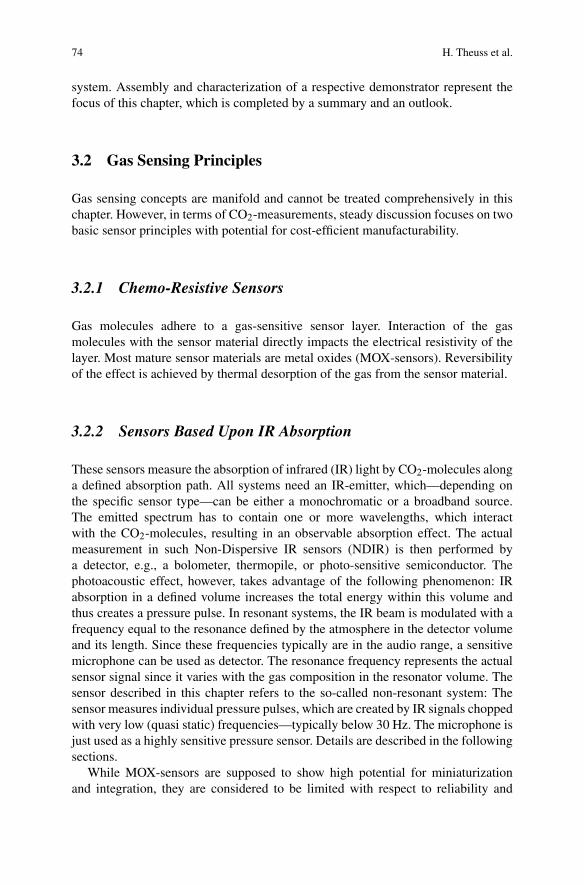
74 H. Theuss et al.
system. Assembly and characterization of a respective demonstrator represent thefocus of this chapter, which is completed by a summary and an outlook.
3.2 Gas Sensing Principles
Gas sensing concepts are manifold and cannot be treated comprehensively in thischapter. However, in terms of CO2-measurements, steady discussion focuses on twobasic sensor principles with potential for cost-efficient manufacturability.
3.2.1 Chemo-Resistive Sensors
Gas molecules adhere to a gas-sensitive sensor layer. Interaction of the gasmolecules with the sensor material directly impacts the electrical resistivity of thelayer. Most mature sensor materials are metal oxides (MOX-sensors). Reversibilityof the effect is achieved by thermal desorption of the gas from the sensor material.
3.2.2 Sensors Based Upon IR Absorption
These sensors measure the absorption of infrared (IR) light by CO2-molecules alonga defined absorption path. All systems need an IR-emitter, which—depending onthe specific sensor type—can be either a monochromatic or a broadband source.The emitted spectrum has to contain one or more wavelengths, which interactwith the CO2-molecules, resulting in an observable absorption effect. The actualmeasurement in such Non-Dispersive IR sensors (NDIR) is then performed bya detector, e.g., a bolometer, thermopile, or photo-sensitive semiconductor. Thephotoacoustic effect, however, takes advantage of the following phenomenon: IRabsorption in a defined volume increases the total energy within this volume andthus creates a pressure pulse. In resonant systems, the IR beam is modulated with afrequency equal to the resonance defined by the atmosphere in the detector volumeand its length. Since these frequencies typically are in the audio range, a sensitivemicrophone can be used as detector. The resonance frequency represents the actualsensor signal since it varies with the gas composition in the resonator volume. Thesensor described in this chapter refers to the so-called non-resonant system: Thesensor measures individual pressure pulses, which are created by IR signals choppedwith very low (quasi static) frequencies—typically below 30 Hz. The microphone isjust used as a highly sensitive pressure sensor. Details are described in the followingsections.
While MOX-sensors are supposed to show high potential for miniaturizationand integration, they are considered to be limited with respect to reliability and
3 Miniaturized Photoacoustic Gas Sensor for CO2 75
long-term stability. For applications requiring higher robustness, the market tendsto prefer optical systems rather than chemo-resistive principles.
3.3 Basics: The Photoacoustic Effect
Depending on their complexity, gas molecules can show a variety of vibrationalmodes. Only a selection of modes which go along with a dipole moment can interactwith electromagnetic radiation. The relevant IR-active oscillation mode for our CO2sensor is an antisymmetric stretching mode as illustrated in Fig. 3.1. Quantummechanics and overlap of the vibration with rotational modes lead to complexabsorption bands (Fig. 3.1).
These absorption bands are very unique for different molecules. Thus, IR absorp-tion can be used for selective detection of specific substances. If this absorptionhappens within a closed volume by a pulsed incoming IR beam, the respectiveabsorbed energy creates a measurable pressure pulse inside this volume. A very highCO2-concentration (close to 100%) in this reference cell increases this signal and atthe same time cares for the gas selectivity of the sensor: In case a light source witha continuous spectrum (black body emitter) is used as IR source, this reference cellconcept selects the relevant absorption lines in an elegant way. Only the absorptionlines associated with the spectrum of the relevant gas (Fig. 3.1) contribute to theheight of the created pressure pulse. This concept makes the implementation of ahigh-quality filter obsolete, which would be necessary in case of a standard NDIRsensor.
Fig. 3.1 Absorption band ofthe antisymmetric stretchingoscillation in a CO2-molecule
76 H. Theuss et al.
3.3.1 Concept of the Sensor
Figure 3.2 illustrates the overall sensor concept: An emitter (Fig. 3.2a), left) emits apulsed IR beam. The intensity spectrum S0(λ) can be a broadband spectrum, butit must contain the relevant gas-specific wavelengths. The beam travels throughthe absorption path where environmental CO2 causes absorption. Figure 3.2bschematically illustrates the absorption and mentions absorption coefficients α1 andα2 corresponding to CO2-concentrations c1 < c2. As we are dealing with a wholeabsorption band (Fig. 3.1) rather than a monochromatic beam, a simple Lambert-Beer type absorption law I(x)/I(0) = e−α c x for the intensity I(x) is not applicable:The coefficients α strongly depend on the wavelength λ. In other words: Individuallines in Fig. 3.1 experience different absorption strengths. This fine structure isnot shown in Fig. 3.2c, but rather summarized in one absorption peak. The IR-pulse corresponding to spectrum Sa eventually hits the reference volume, where it
Sensor signal
Reference path
Inte
nsi
ty
I
Ia IbIo
λ0
S0 gas concentration c1
gas concentration c2 > c1
λ0
Sb
λ0
Sa
a)
b)
c)
Emitter Detector
Absorption path
Fig. 3.2 Concept of the sensor. (a) Physical system showing broadband emitter (left), absorptionpath (with typically low CO2-concentration) and detector containing MEMS microphone and othercomponents. Detector components are enclosed into a cavity which contains a high concentrationof CO2, (b) Illustration of intensity distribution along absorption and reference path. Also shownare pressure signals corresponding to two CO2-concentrations c1 < c2. The steps in the chart on theright refer to increasing CO2-concentrations separated by evacuation steps. (c) Schematic spectrumas provided by the emitter (left), after penetration through the absorption path (middle) and afterpassing through the reference cell (right)
3 Miniaturized Photoacoustic Gas Sensor for CO2 77
experiences a much higher absorption due to the high CO2-concentration cr >> c1,c2. In the reference cell, molecules in the excited vibration state very quickly relaxby transferring their oscillation energy into translation energy via hits with othermolecules (typical relaxation time ∼10−4 s). In consequence, the temperature Tincreases. Part of the absorbed energy then translates into a pressure pulse via pVr∼T (where Vr is the volume of the reference cell). This is the photoacoustic pressureas detected by the MEMS microphone (Micro Electro Mechanical System). Anotherpart of the absorbed energy escapes by heat dissipation into and through the walls ofthe reference cell. The spectra Sa and Sb in Fig. 3.2c show the condition of the IR-pulse prior and after passing through the reference cell. These spectra correspond tothe respective intensities Ix (x = 0, a, b) mentioned in Fig. 3.2b. Figure 3.2c nicelyexplains the gas selectivity of the sensor: Only the gas-specific absorption linescontribute to the photoacoustic effect. The spectrum outside the absorption band ofCO2 does not.
An increase of the concentration in the absorption path from c1 to c2 > c1 leads toincreased absorption (lower Ia). However, this translates into a lower photoacousticpressure pulse p2 since the absorption in the reference cell starts at this lower levelof Ia. Thus, higher CO2-concentrations in the absorption path (environment) createlower photoacoustic pressure pulses. In order to actually probe the concentration,increase from c1 to c2, the sensor needs to resolve the photoacoustic pressuredifference p1 − p2 ∼c2 – c1.
3.4 Translation into Package and System Requirements
The necessary emitter of such a system needs to emit a spectrum containing therelevant absorption bands in a relatively high intensity. Luckily, this is the case for avariety of MEMS emitters. These provide a spectrum close to a black body radiationwith a maximum around 4 μm.
A suitable MEMS microphone must be tuned with respect to its cut-off fre-quency, which needs to fit to the modulation frequency of the emitter (typically10–30 Hz).
In order to ensure the functionality of the sensor and to avoid drift effects, theCO2-concentration in the reference cell needs to be constant through the lifetime ofthe sensor. In consequence, the reference cell must be sealed hermetically. At thesame time, it must be filled with a high concentration of CO2.
Lid materials for emitter and detector package must be highly transparent forwavelengths in the 4.3 μm range in order not to lose too much intensity by reflectionand absorption.
Finally, the dimensions of the sensor, especially the lengths of absorption andreference paths must be compromised with the requirement to make a miniaturizedsystem.
78 H. Theuss et al.
3.5 Ceramic Package Concept
As polymer materials still show a certain permeability for gases, plastic encap-sulation is not an option to fulfill the required hermeticity level. The remainingoptions are metal can packages and ceramic packaging. Through hole metal cantechnology—frequently called TO-packaging (Transistor Outline)—is rather oldfashioned but provides a reliable sealing process by resistance welding. The conceptin Fig. 3.1 has already been demonstrated on the basis of TO-packaging [1]. Herethe target is to further miniaturize the system by making use of ceramic cavitypackaging, which offers flexible routing capability along with SMT mount ability(Surface Mount Technology).
Both emitter and detector components were die−/wire-bonded into standardHTCC cavity packages (High Temperature Cofired Ceramics)—size approx.9×9 mm2. Optical sapphire windows were chosen due to their good IR-transmissionproperties. Hermetic sealing was achieved by a soldering process using respectivemetal stacks both on the ceramic cavity and the sapphire lid together with a frame-shaped AuSn preform. The solder process for the lid attach of the detector wasperformed in CO2-atmosphere in order to enclose the gas in the reference cell.
Now emitter and detector need to be aligned face to face to each other in order toreproduce the situation schematically illustrated in Fig. 3.2. If the emitter is chosenas top component, a simple but efficient approach is shown in Fig. 3.3: The twoelectrical contacts are routed to the bottom using appropriate metal pieces. Thisenables later SMD-assembly (Surface Mount Device) onto a printed circuit board(PCB).
3.6 Hermeticity
Hermeticity is the effectiveness of the seal of microelectronic devices with designedinternal cavities [2] and by design, a hermetic seal prevents gases and liquids fromentering the package cavity where the die is mounted [3]. Hermeticity can bedescribed by a supportive quality property called leak rate.
There are different backgrounds for the emitter and detector package why ahermetic seal is required. While the emitter needs to enclose a protective gas (e.g.,N2) inside the cavity for reliability reason the detector needs to provide the referencegas filling inside the sealed cavity for functionality of the sensor device.
There are three major reliability aspects which potentially can harm the inertgas atmosphere within the hermetic sealed cavity with respect to its initial state.First, there are capillary leaks leading to viscous or molecular gas flow. Second,there is permeation which is a function of adsorption on a package material surface,diffusion through this permeate, and desorption on the opposite surface to gasinterface. And last, there are outgassing effects of polymers or trapped moleculesin bulk materials. The initial state of the enclosed gas atmosphere is represented
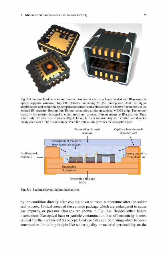
3 Miniaturized Photoacoustic Gas Sensor for CO2 79
Fig. 3.3 Assembly of detector and emitter into ceramic cavity packages, sealed with IR-permeableoptical sapphire windows. Top left: Detector containing MEMS microphone, ASIC for signalamplification and conditioning, temperature sensor, and a photodiode to observe fluctuations in theemitted IR-intensity. Bottom left: Emitter containing a micromachined MEMS-chip. The emitterbasically is a resistor designed to emit a maximum amount of input energy as IR-radiation. Thus,it has only two electrical contacts. Right: Example for a subassembly with emitter and detectorfacing each other. The distance in between the optical lids provides the absorption path
Fig. 3.4 Sealing relevant failure mechanisms
by the condition directly after cooling down to room temperature after the solderseal process. Critical zones of the ceramic package which are endangered to causegas impurity or pressure changes are shown in Fig. 3.4. Besides other failuremechanisms like optical haze or particle contamination, loss of hermeticity is mostcritical for the ceramic PAS concept. Leakage fails can be distinguished betweenconstruction limits in principle like solder quality or material permeability on the
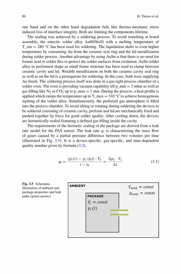
80 H. Theuss et al.
one hand and on the other hand degradation fails like thermo-mechanic stressinduced loss of interface integrity. Both are limiting the components lifetime.
The sealing was achieved by a soldering process. To avoid remelting at boardassembly, the eutectic solder alloy Au80/Sn20 with a melting temperature ofT_eut = 280 ◦C has been used for soldering. The liquidation shifts to even highertemperature by consuming Au from the ceramic seal ring and the lid metallizationduring solder process. Another advantage by using AuSn is that there is no need forformic acid or solder flux to protect the solder surfaces from oxidation. AuSn solderalloy in preformed shape as small frame structure has been used to clamp betweenceramic cavity and lid. Wetable metallization on both the ceramic cavity seal ringas well as on the lid is a prerequisite for soldering. In this case, both were supplyingAu finish. The soldering process itself was done in a gas tight process chamber of asolder oven. The oven is providing vacuum capability till p_min = 3 mbar as well asgas filling like N2 or CO2 up to p_max = 1 atm. During the process, a heat profile isapplied which ramps the temperature up to T_max = 310 ◦C to achieve homogenousmelting of the solder alloy. Simultaneously, the preferred gas atmosphere is filledinto the process chamber. To avoid tilting or rotating during soldering the devices tobe soldered consisting of ceramic cavity, preform and lid are mechanically fixed andpushed together by force for good solder quality. After cooling down, the devicesare hermetically sealed featuring a defined gas filling inside the cavity.
The requirements of the hermetic sealing of the package are derived from a leakrate model for the PAS sensor. The leak rate ql is characterizing the mass flowof gases caused by a partial pressure difference between two volumes per time(illustrated in Fig. 3.5). It is a device-specific, gas-specific, and time-dependentquality number given by formula (3.2).
ql = |pc(t) − pc (t0)| · Vc
t − t0= pc · Vc
t(3.1)
Fig. 3.5 Schematicillustration of ambient andpackage properties and leakpaths (green arrows)
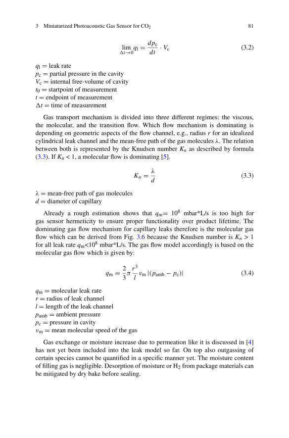
3 Miniaturized Photoacoustic Gas Sensor for CO2 81
limt→0
ql = dpc
dt· Vc (3.2)
ql = leak ratepc = partial pressure in the cavityVc = internal free-volume of cavityt0 = startpoint of measurementt = endpoint of measurementt = time of measurement
Gas transport mechanism is divided into three different regimes: the viscous,the molecular, and the transition flow. Which flow mechanism is dominating isdepending on geometric aspects of the flow channel, e.g., radius r for an idealizedcylindrical leak channel and the mean-free path of the gas molecules λ. The relationbetween both is represented by the Knudsen number Kn as described by formula(3.3). If Kn < 1, a molecular flow is dominating [5].
Kn = λ
d(3.3)
λ = mean-free path of gas moleculesd = diameter of capillary
Already a rough estimation shows that qm= 108 mbar*L/s is too high forgas sensor hermeticity to ensure proper functionality over product lifetime. Thedominating gas flow mechanism for capillary leaks therefore is the molecular gasflow which can be derived from Fig. 3.6 because the Knudsen number is Kn > 1for all leak rate qm<108 mbar*L/s. The gas flow model accordingly is based on themolecular gas flow which is given by:
qm = 2
3π
r3
lvm |(pamb − pc)| (3.4)
qm = molecular leak rater = radius of leak channell = length of the leak channelpamb = ambient pressurepc = pressure in cavityνm = mean molecular speed of the gas
Gas exchange or moisture increase due to permeation like it is discussed in [4]has not yet been included into the leak model so far. On top also outgassing ofcertain species cannot be quantified in a specific manner yet. The moisture contentof filling gas is negligible. Desorption of moisture or H2 from package materials canbe mitigated by dry bake before sealing.
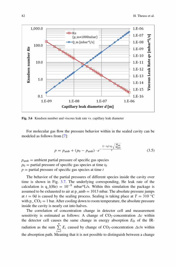
82 H. Theuss et al.
Fig. 3.6 Knudsen number and viscous leak rate vs. capillary leak diameter
For molecular gas flow the pressure behavior within in the sealed cavity can bemodeled as follows from [7]:
p = pamb + (p0 − pamb) · e−(t−t0)·ql·
√MairMgas
V (3.5)
pamb = ambient partial pressure of specific gas speciesp0 = partial pressure of specific gas species at time t0p = partial pressure of specific gas species at time t
The behavior of the partial pressures of different species inside the cavity overtime is shown in Fig. 3.7. The underlying corresponding, He leak rate of thecalculation is q_l(He) = 10−9 mbar*L/s. Within this simulation the package isassumed to be exhausted to air at p_amb = 1013 mbar. The absolute pressure jumpsat t = 0d is caused by the sealing process. Sealing is taking place at T = 310 ◦Cwith p_ CO2 = 1 bar. After cooling down to room temperature, the absolute pressureinside the cavity is nearly cut into halves.
The correlation of concentration change in detector cell and measurementsensitivity is estimated as follows: A change of CO2-concentration Δc withinthe detector cell causes the same change in energy absorption ED of the IR-
radiation as the sumn∑
i=1Ei caused by change of CO2-concentration Δc/n within
the absorption path. Meaning that it is not possible to distinguish between a change
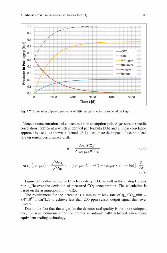
3 Miniaturized Photoacoustic Gas Sensor for CO2 83
Fig. 3.7 Simulation of partial pressures of different gas species in soldered package
of detector concentration and concentration in absorption path. A gas sensor-specificcorrelation coefficient a which is defined per formula (3.6) and a linear correlationapproach is used like shown in formula (3.7) to estimate the impact of a certain leakrate on sensor performance drift.
a = cc (CO2)
cabs path (CO2)(3.6)
qCO2
(cabs path
) =√
MCO2√MHe
· a · [cabs path(t) · pc(t) − cabs path (t0) · pc (t0)] · Vc
t
(3.7)
Figure 3.8 is illustrating the CO2 leak rate q_ CO2 as well as the analog He leakrate q_He over the deviation of measured CO2-concentration. The calculation isbased on the assumption of a = 0.25.
The requirement for the detector is a minimum leak rate of q_ CO2_min =7.4*1012 mbar*L/s to achieve less than 200 ppm sensor output signal drift over2 years.
Due to the fact that the target for the detector seal quality is the more stringentone, the seal requirement for the emitter is automatically achieved when usingequivalent sealing technology.
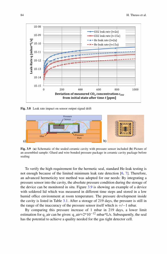
84 H. Theuss et al.
Fig. 3.8 Leak rate impact on sensor output signal drift
Fig. 3.9 (a) Schematic of the sealed ceramic cavity with pressure sensor included (b) Picture ofan assembled sample: Glued and wire bonded pressure package in ceramic cavity package beforesealing
To verify the high requirement for the hermetic seal, standard He-leak testing isnot enough because of the limited minimum leak rate detection [6, 7]. Therefore,an advanced hermeticity test method was adopted for our needs: By integrating apressure sensor into the cavity, the absolute pressure condition during the storage ofthe device can be monitored in situ. Figure 3.9 is showing an example of a devicewith soldered lid which was measured in different time steps and stored in a lowhumid office environment at room temperature. The pressure development insidethe cavity is listed in Table 3.1. After a storage of 219 days, the pressure is still inthe range of the inaccuracy of the pressure sensor itself which is +/−1 mbar.
By comparing this pressure increase of 1 mbar in 219 days, a lower limitestimation for q_air can be given: q_air≈2*10−12 mbar*L/s. Subsequently, the sealhas the potential to achieve a quality needed for the gas tight detector cell.
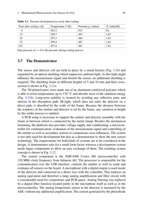
3 Miniaturized Photoacoustic Gas Sensor for CO2 85
Table 3.1 Pressure development in cavity after sealing
Time after sealing t [d] Temperature T [K] Pressure pc [mbar] pcT
[mbar/K]
0 583.2 815 Na15 299.7 487 1,6324 297.2 484 1,6335 299.4 487 1,63
219 297.6 481 1,62
Start pressure at t = 0 is the pressure during sealing process
3.7 The Demonstrator
The sensor and detector cell are held in place by a metal bracket (Fig. 3.10) andseparated by an optical shielding which suppresses ambient light. As this light mightinfluence the measurement signal and disturb the sensor, an additional shielding isrequired. The shielding frame in different heights of 5 and 10 mm and their cross-section is shown in Fig. 3.11a.
The 3D-printed parts were made out of an aluminum reinforced polymer whichis able to resist temperatures up to 130 ◦C and absorbs most of the radiation energy(Fig. 3.11b). Long-term stability is insured by avoiding any reflective parts andmirrors in the absorption path. IR-light, which does not enter the detector on adirect path, is absorbed by the walls of the frame. Because the distance betweenthe windows of the emitter and detector is set by the frame, any variation in heightby the solder process is omitted.
A PCB setup is necessary to support the emitter and detector assembly with theframe in between which is connected by the metal clamp. Besides the mechanicalmounting, the platform also provides voltage supply and conditioning, a microcon-troller for communication, evaluation of the measurement signal and controlling ofthe emitter as well as secondary sensors to compensate cross influences. The systemis not only used for development but also as a demonstrator to show the new sensortechnology. The requirements for both kinds of systems are to be considered in thedesign. A demonstrator asks for a small form factor whereas a development systemneeds larger components to allow an easy exchange of them. The resulting systemconcept is shown in Fig. 3.12.
The central component is the XMC4400 Cortex M4 microcontroller with120 MHz clock frequency from Infineon AG. The processor is responsible for thecommunication over the USB interface, controls the emitter as well as reads andevaluates all sensors on the board. A microphone with a digital output is used insideof the detector and connected in a direct way with the controller. This replaces ananalog equivalent and therefore a large analog amplification and filter circuit witha considerable need for components and PCB-space. Analog filtering was replacedby a digital filter function located partly in the microphone itself as well as in themicrocontroller. The analog temperature sensor in the detector is measured by theADC without any additional amplification. The current generated by the photodiode
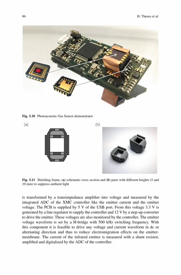
86 H. Theuss et al.
Fig. 3.10 Photoacoustic Gas Sensor demonstrator
Fig. 3.11 Shielding frame, (a) schematic cross section and (b) parts with different heights (5 and10 mm) to suppress ambient light
is transformed by a transimpedance amplifier into voltage and measured by theintegrated ADC of the XMC controller like the emitter current and the emittervoltage. The PCB is supplied by 5 V of the USB port. From this voltage 3.3 V isgenerated by a line regulator to supply the controller and 12 V by a step-up converterto drive the emitter. These voltages are also monitored by the controller. The emittervoltage waveform is set by a H-bridge with 500 kHz switching frequency. Withthis component it is feasible to drive any voltage and current waveform in dc oralternating direction and thus to reduce electromigration effects on the emitter-membrane. The current of the infrared emitter is measured with a shunt resistor,amplified and digitalized by the ADC of the controller.
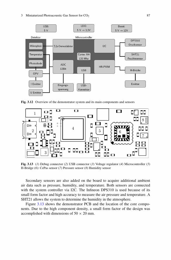
3 Miniaturized Photoacoustic Gas Sensor for CO2 87
Fig. 3.12 Overview of the demonstrator system and its main components and sensors
Fig. 3.13 (1) Debug connector (2) USB connector (3) Voltage regulator (4) Microcontroller (5)H-Bridge (6): CePas sensor (7) Pressure sensor (8) Humidity sensor
Secondary sensors are also added on the board to acquire additional ambientair data such as pressure, humidity, and temperature. Both sensors are connectedwith the system controller via I2C. The Infineon DPS310 is used because of itssmall form factor and high accuracy to measure the air pressure and temperature. ASHT21 allows the system to determine the humidity in the atmosphere.
Figure 3.13 shows the demonstrator PCB and the location of the core compo-nents. Due to the high component density, a small form factor of the design wasaccomplished with dimensions of 50 × 20 mm.
88 H. Theuss et al.
3.8 Reliability of PAS-Gas Sensors
3.8.1 PAS-Gas Sensor for Automotive Applications
As told before, within automotive vehicles there is a broad field of applications forGas Sensors.
One example is CO2 leakage detection in case of using CO2 as a cooling medium.Another application is intelligent air conditioning, where the air exchange is
driven by air quality. A further use case is presence detection, where a change ora not change of the CO2 level in the car indicates the presence of persons, e.g.,babies.
But to use a PAS sensor for these applications, the automotive reliability criteriahave to be fulfilled.
To address thus topic, first of all an assessment of the underlying physicalprinciples has to be done. The physical principle determines the failure mechanisms.
In the case of PAS-Gas sensor, the principle is a pure physical volume concept.Radiation is absorbed and converted into heat and heat is converted into a pressuresignal. If the radiation is chopped, it results in a sound signal. There are no chemicalchanges in surfaces, no need for reconditioning, and no degradation of components.
A second aspect of this physical concept is that due to the feasibility of lowdegradation or drift an absolute value can be calculated.
3.8.2 PAS-Gas Sensor Automotive Requirements
Main requirements for automotive applications are as follows:
• An extended temperature range from −40 ◦C to about 125 ◦C.• Temperature robustness for standard MEMS devices and integrated circuits in
the detector is given. No degradation expected here.• Extended humidity range up to 95% rH.• Closed cavity emitter and closed cavity detector sensor components give envi-
ronmental robustness.• Limited supply voltage below 12 V.• 12 V is a supply voltage which can be handled can be provided in standard
integrated circuits.• Limited power consumption in standby mode < 1 mA.• The PAS sensor using high sensitive microphones allows a broad variation of
adaption to different applications. High emitter temperatures in combination witha high measurement frequency enable high resolution in concentration and time.Low emitter temperatures in combination with a low measurement frequencyenable high robustness and long lifetime.
• Strong requirements about chemical robustness of the system in an automotiveenvironment.

3 Miniaturized Photoacoustic Gas Sensor for CO2 89
• Closed cavity emitter and closed cavity detector components enable a highenvironmental robustness.
• Failure rate is according to automotive standards.• Usage of standard integrated components like the control ASICs and standard
MEMS components like the microphone and ASIC and well-known packagesenable sensor with known failure rates over lifetime.
• Feasible performance of the sensor over a lifetime of 15 years.• Usage of standard integrated components (like microphone and ASIC, standard
packages, etc.) with known failure rate.
3.9 Reliability Providing Building Blocks
A main advantage of the PAS-Gas Sensor is its underlying concept.The physics on which the concept is based is radiation absorption in a gas
volume. Therefore, there is no surface which changes, which can degrade, whichcan be contaminated, or which has to be refreshed.
A second building block, also based on the concept, is that the development of aphysical model.
A model, which can explain the performance and the functionality of the sensor,can also be used to explain deviation. In addition, such a model can help to easilyadapt to the setup of the sensor, to avoid failure mechanisms and to make the sensormore robust.
A third building block of reliability is the qualification of the sensor according toautomotive rules.
This must be topic of further PAS sensor development. In addition, in this case themodel will help to find appropriate tests. A main task here will be the developmentof test, which can accelerate the aging of the sensor. The development of tests withknown activation energies regarding aging will be used to show the feasibility of arobust sensor. In addition, the availability of those tests accelerates the developmentof optimized sensors and sensor modules.
3.10 Characterization of the Demonstrator
The system was placed in an aluminum housing with two gas fittings. This allowsto measure the response time due to its small volume and to pressurize the systemdue to its rigid design (Fig. 3.14).
Systematic measurements to characterize the system behavior were conducted.Therefore, different gas concentrations of CO2 at different environmental conditionslike temperature, pressure, and humidity were flown into the sample cell.
The measurement of the sensitivity shows a standard deviation of 25 ppm at100 ppm CO2-concentration and up to 60 ppm at 40,000 ppm. A significant but
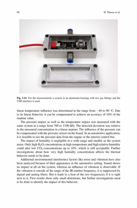
90 H. Theuss et al.
Fig. 3.14 For the measurements a system in an aluminum housing with two gas fittings and theUSB interface is used
linear temperature influence was determined in the range from −40 to 90 ◦C. Dueto its linear behavior, it can be compensated to achieve an accuracy of 10% of thereadout value.
The pressure impact as well as the temperature impact was measured with thesame system in a range from 700 to 1100 hPa. The detected deviation was relativeto the measured concentration in a linear manner. The influence of the pressure canbe compensated with the pressure sensor on the board. In an automotive application,it is feasible to use the pressure data from the engine or the interior control bus.
The impact of humidity is negligible in a wide range and smaller as the systemnoise. Only high H2O concentrations at high temperature and high relative humiditycould alter low CO2-concentrations up to 10%, which is still acceptable. Furtherinvestigations about how very high humidity concentration affects the thermalbehavior needs to be done.
Additional environmental interference factors like noise and vibration have alsobeen analyzed because of their appearance in the automotive setting. Sound showsno impact at all on the system, whereas an influence of vibration is observable. Ifthe vibration is outside of the range of the IR-emitter frequency, it is suppressed bydigital and analog filters. But it leads to a beat of the two frequencies if it is rightnext to it. First results show only small distortions, but further investigations needto be done to identify the impact of this behavior.
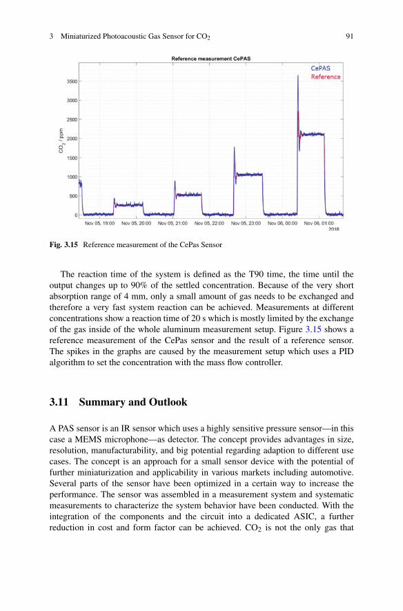
3 Miniaturized Photoacoustic Gas Sensor for CO2 91
Fig. 3.15 Reference measurement of the CePas Sensor
The reaction time of the system is defined as the T90 time, the time until theoutput changes up to 90% of the settled concentration. Because of the very shortabsorption range of 4 mm, only a small amount of gas needs to be exchanged andtherefore a very fast system reaction can be achieved. Measurements at differentconcentrations show a reaction time of 20 s which is mostly limited by the exchangeof the gas inside of the whole aluminum measurement setup. Figure 3.15 shows areference measurement of the CePas sensor and the result of a reference sensor.The spikes in the graphs are caused by the measurement setup which uses a PIDalgorithm to set the concentration with the mass flow controller.
3.11 Summary and Outlook
A PAS sensor is an IR sensor which uses a highly sensitive pressure sensor—in thiscase a MEMS microphone—as detector. The concept provides advantages in size,resolution, manufacturability, and big potential regarding adaption to different usecases. The concept is an approach for a small sensor device with the potential offurther miniaturization and applicability in various markets including automotive.Several parts of the sensor have been optimized in a certain way to increase theperformance. The sensor was assembled in a measurement system and systematicmeasurements to characterize the system behavior have been conducted. With theintegration of the components and the circuit into a dedicated ASIC, a furtherreduction in cost and form factor can be achieved. CO2 is not the only gas that

92 H. Theuss et al.
Table 3.2 Sensor absorptionlevels
Gas Main absorption
CH4 3.3 μmCO2 4.3 μmCO 4.6 μmNO 5.3 μmNO2 6.2 μmN2O 7.7 μm
can be detected by this kind of sensor. The filling of the reference chamber onlyneeds to be exchanged in order to change the gas selectivity (Table 3.2) [8].
Gas sensing is one of the key topics in the area of environmental sensing.Besides the automotive sector [9], consumer markets with air quality applicationsalso require a huge number of cheap devices. The new sensor system based onthe photoacoustic effect and realized in a ceramic package perfectly suits therequirements of a modern and state-of-the-art gas sensor for the high-volumemarket.
References
1. T.H. Tille, Automobil-Sensorik: Ausgewählte Sensorprinzipien und deren automobile Anwen-dung. 1. Auflage (Springer, Berlin, 2016). ISBN 978-3-6624-8943-7
2. Department of Defense, MIL-STD-883K: Test Method Standard Microcircuits (Department ofDefense, Columbo, OH, 2016)
3. National Semiconductor Corporation, Semiconductor Packaging Assembly Technology(National Semiconductor, Santa Clara, CA, 1999). www.national.com
4. D. Stroehle, On the penetration of gases and water vapour into packages with cavities and onmaximum allowable leak rates, in 15th International Reliability Physics Symposium, Las Vegas(Nevada), (1977), pp. 101–106. https://doi.org/10.1109/IRPS.1977.362778
5. S. Costello, M.P.Y. Desmulliez, Hermeticity testing of MEMS microelectronic packages, 1st edn.(Artech House, Norwood, 2013). ISBN 978-1-6080-7527-0
6. S. Costello, M.P.Y. Desmulliez, S. Mccracken, Review of test methods used for the measurementof hermeticity in packages containing small cavities, in IEEE Transactions on Components,Packaging and Manufacturing Technology, ed. by S. Costello et al., vol. 2, (2012), pp. 430–438.https://doi.org/10.1109/TCPMT.2011.2176122
7. H. Greenhouse, Hermeticity of Electronic Packages, 2nd edn. (Elsevier, Amsterdam, 2011).ISBN 978-1-4377-7877-9
8. “HITRAN spectral database,” 2016 [online] https://www.cfa.harvard.edu/hitran/9. S.A. Abdul-Wahab, S.C.F. En, A. Elkamel, L. Ahmadi, K. Yetilmezsoy, A review of standards
and guidelines set by international bodies for the parameters of indoor air quality. Atmos. Pollut.Res. 5, 751–767 (2015)
Chapter 4Multipath Ray-Tracing-Based Modellingof Time-of-Flight Cameras
Method and Application to Semi-Transparent andScattering Media
Marcus Baumgart, Norbert Druml, and Cristina Consani
4.1 Introduction and Related Work
The intent of this section is to give a brief overview on optical Time-of-Flight (ToF)sensors and technologies, with a special focus on implementations for ranging.After a brief introduction on current ranging technologies, the working principleof ToF sensors is discussed in more detail. In particular, we will briefly reviewexisting simulation frameworks that allow modelling a ToF sensor response, andthe challenges imposed by multipath interference effects not only on the sensoraccuracy, but also on the realization of an accurate and predictive sensor simulationenvironment.
4.1.1 Optical Range Detection
Fast and reliable classification of the environment is considered an evolutionaryadvantage. Range detection based on light started evolving millions of years agoand since then continuously specialized and improved in nature. A very familiarexample of light-based range sensing and 3D perception is given by the humaneyes. The human eye can be classified as a passive optical range detector becauseit only relies on illumination from environmental light sources, like the sun, todetect objects and estimate their positions. The light is converted in the eye’s retina
M. Baumgart · C. Consani (�)Photonic Systems, CTR Carinthian Tech Research AG, Villach, Austriae-mail: [email protected]
N. DrumlInfineon Technologies Austria AG, Graz, Austria
© Springer Nature Switzerland AG 2020W. D. van Driel et al. (eds.), Sensor Systems Simulations,https://doi.org/10.1007/978-3-030-16577-2_4
93
94 M. Baumgart et al.
into electrical neural impulses which are decoded by the brain to perform visualperception. A single eye uses a variety of strategies known as monocular visualcues to estimate the distance of an object and the relative position of different objectsin space. Among such strategies are the size of a familiar object on the retina, therelative sizes of familiar objects, visual overlap of objects, linear perspective, motionparallax, relative position, and/or interposition of shadows, as well as defocusingand refocusing techniques which allow inferring the distance of an object fromthe contraction of the muscles of the eye. Although most of these strategies onlyprovide cues on the relative distances between different objects present in the scene,continuous training and the resulting experience enables good absolute distanceestimations even for monocular vision [1–3].
With the combination of the visual information from both eyes (binocular vision,or stereovision) the human vision system becomes a very good range sensor. Whenwe observe an object first with one eye and then with the other, we realize thatthe images from the two eyes differ. This phenomenon is called “retinal disparity”:Since the eyes are horizontally separated, the projection of the same object on theretina differs between the two eyes, with a difference that decreases with longerdistances. Our brain “decodes” the information contained in this retinal disparityand returns a single image with a good estimation of the location of the objects inthe 3D space. This principle is of course known and very well understood, and it isat the basis of triangulation techniques. Most “passive” optical ranging techniqueswere initially inspired by human vision, and later on further optimized.
Range detection systems can be divided into “passive illumination” and “activeillumination” systems. Passive illumination systems are the direct analog to humaneyes: they use external illumination sources (e.g., sunlight) and adopt specificstrategies to evaluate the distance of surrounding objects. Just like people caninfer distance information from monocular cues, several techniques using a singlecamera aided by specially designed smoothing and image-recognition algorithmshave been developed for ranging. Examples are depth from focus and defocus [4],or monocular Simultaneous Localization and Mapping (SLAM) [5]. However, themost common strategies are inspired by binocular vision. The main idea behindstereovision is to observe the same scene with two cameras that are separated bysome distance in space. Completely analogous to what happens in human eyes,the projection of the same scene on the two cameras differs due to the distancebetween them, and a disparity map can be constructed (which, in the simplestcase, is computed from the difference between the pixel locations of the sameobject position on the two cameras). As the disparity is inversely proportionalto the distance of the objects, the depth of the scene can be reconstructed. Suchtriangulation schemes allow reconstructing the positions of object points within athree-dimensional scene, provided that several unique corresponding points in bothimages (within the common field of view of the two cameras) can be identified. Thisrequirement is also known as the “correspondence problem” and it can be difficult tosatisfy in practice, especially for multi-camera systems in front of arbitrary scenes.Much software development in the direction of image processing (e.g., to correct forlens distortions), image recognition, and modelling is active in this directionbreak
4 Multipath Ray-Tracing-Based Modelling of Time-of-Flight Cameras 95
[6–8]. Nowadays stereo cameras combined with advanced algorithms can be usedfor detection, recognition, and distance estimation of static scenes, as well as formotion tracking for a large variety of scenes. An in-depth introduction to this topic isgiven in [9–11]. Extending this scheme to include more cameras at different angleswill result in a more precise description of the three-dimensional scene. This isthe idea behind lightfield imaging. In most implementations, a lightfield cameraincludes a micro-lens array in front of a conventional 2D pixelated detector so thata large number of images from different angular perspectives can be acquired in asingle shot.
All these techniques rely on external light sources. If the available environmentallight sources are not sufficient, a dedicated light source can be used (e.g., using atorch on a night walk enables us to see and detect objects in the absence of sufficientenvironmental light). Since the source characteristics do not affect the detectionscheme, no other requirement is imposed on the source other than being intenseenough to illuminate the scene at a level that is sufficient for detection.
Active illumination detection systems by contrast require a dedicated illumina-tion source and specific knowledge about the projected light. The term “active”implies that not only the source is part of the sensor itself, but that differentillumination patterns (structured or coded light) are projected (in space and/or intime) onto the scene. The 3D coordinates of the objects in the scene are thenreconstructed using the response of the sensor to the multiple illumination patterns.In general, three main principles can be employed for active illumination systems:triangulation-based schemes, round-trip time-dependent schemes and wave-mixingschemes.
In the torch example above, further information about the torch, like the illumi-nation characteristic and the position relative to the eyes, may enable a more precise3D reconstruction (active triangulation) compared to purely passive detectionmethods. For example, the appearance and shape of shades in combination with thelight source parameters will improve the robustness of the estimation of the objectpositions (image pattern recognition). Alternatively, the projection of an artificialpattern placed in front of the light source can introduce further structure into thescene (pattern projection). The knowledge of the pattern’s structure adds an overlay“mask” to the objects being imaged. Upon proper design of the pattern, a uniquecorrespondence between emitted and observed features can be established, whichallows for a precise reconstruction of distances. These special coding/decodingstrategies are known as coded structured light (CSL) and are at the basis of severalwell-known ranging systems [12], including the first (2010) Microsoft Kinect™camera [13]. When a second pattern is inserted in front of the detector in additionto the projection pattern, object geometry reconstruction based on shadow Moiréinterferences can be performed [14].
An additional opportunity to measure distances with active illumination becomesevident if we realize that there is more information encoded in a reflected lightbeam than just its intensity and angular distribution. As light travels through air at aconstant finite speed, the time it takes for a short light pulse to travel to a distantobject and back is a direct measure of the object distance. For pulsed sources,
96 M. Baumgart et al.
this time delay can be directly measured with a very fast opto-electrical detectorsynchronized with the light source although in most common applications indirectmethods (also called correlation methods) using slower detectors are implemented.The round-trip time measurement with a pulsed or modulated (intensity modulatedor frequency modulated) light source is known as optical Time-of-Flight (ToF) andwill be the focus of the rest of this chapter.
While the ToF schemes mentioned above use external modulation of the lightsource, the intrinsic oscillation of the light electric field can also be employedto measure distances. Since the oscillation frequencies are much higher than theresponse times of available detectors, interferometry has to be used. In the simplestinterferometric scheme, a beam is split into a reference and a measurement beamtravelling through different optical paths. The difference in optical path lengthbetween the two beams is obtained by measuring the interference obtained whenrecombining the two beams on the detector. For a monochromatic source withwavelength λ, measuring the intensity at the detector only allows to retrieve arelative phase difference between the two beams, corresponding to a maximumunambiguous depth range of λ/2. Continuously counting the number of interferencefringes allows tracking larger distance changes, provided the direction of thedistance change is known. The unambiguity in the direction can be removed withlittle effort using quadrature detection. The distance measurement remains, however,a relative measurement.
Performing interferometry at different light frequencies simultaneously (multi-wavelength interferometry) allows extending the unambiguity range. If sufficientlymany different light frequencies are used, the unambiguous range can be extended tospan all expected target distances (thus being equivalent to an absolute distance mea-surement) while maintaining interferometric accuracy as determined by the shortestused wavelength. This is the basic principle of optical coherent tomography (OCT)in the frequency domain. The approach requires a highly complex sensor systemand may become unfeasible if a large measurement range is required. Heterodyneinterferometry often provides a good alternative. Here two different light frequenciesfrom the measurement and reference paths, respectively, are brought to interfere.In practice, this is realized by generating a sideband of a laser source using anoptical modulator. After recombination, this generates a modulated signal with thebeat frequency ν = |ν1 − ν2|. The unambiguous range can be made arbitrarilylarge if the frequency difference is made sufficiently small. The disadvantage isthe lower accuracy now determined by the heavily enlarged synthetic wavelength.Implementations where more than two frequencies are used or where the distance ismeasured at several beat frequencies by changing the frequency in the referenceor measurement arm allow for getting a large unambiguous range while stillmaintaining good accuracy.
Another approach employs frequency sweeping of a narrowband light sourceand uses interferometry to determine the frequency shift of the returning light,which is proportional to the round-trip time. The frequency shift between thereference arm and the measurement arm is measured as a beat frequency anddepends on the absolute path length difference between light travelling through
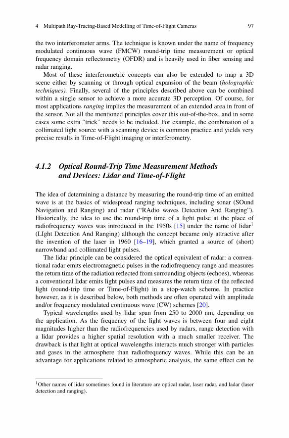
4 Multipath Ray-Tracing-Based Modelling of Time-of-Flight Cameras 97
the two interferometer arms. The technique is known under the name of frequencymodulated continuous wave (FMCW) round-trip time measurement or opticalfrequency domain reflectometry (OFDR) and is heavily used in fiber sensing andradar ranging.
Most of these interferometric concepts can also be extended to map a 3Dscene either by scanning or through optical expansion of the beam (holographictechniques). Finally, several of the principles described above can be combinedwithin a single sensor to achieve a more accurate 3D perception. Of course, formost applications ranging implies the measurement of an extended area in front ofthe sensor. Not all the mentioned principles cover this out-of-the-box, and in somecases some extra “trick” needs to be included. For example, the combination of acollimated light source with a scanning device is common practice and yields veryprecise results in Time-of-Flight imaging or interferometry.
4.1.2 Optical Round-Trip Time Measurement Methodsand Devices: Lidar and Time-of-Flight
The idea of determining a distance by measuring the round-trip time of an emittedwave is at the basics of widespread ranging techniques, including sonar (SOundNavigation and Ranging) and radar (“RAdio waves Detection And Ranging”).Historically, the idea to use the round-trip time of a light pulse at the place ofradiofrequency waves was introduced in the 1950s [15] under the name of lidar1
(LIght Detection And Ranging) although the concept became only attractive afterthe invention of the laser in 1960 [16–19], which granted a source of (short)narrowband and collimated light pulses.
The lidar principle can be considered the optical equivalent of radar: a conven-tional radar emits electromagnetic pulses in the radiofrequency range and measuresthe return time of the radiation reflected from surrounding objects (echoes), whereasa conventional lidar emits light pulses and measures the return time of the reflectedlight (round-trip time or Time-of-Flight) in a stop-watch scheme. In practicehowever, as it is described below, both methods are often operated with amplitudeand/or frequency modulated continuous wave (CW) schemes [20].
Typical wavelengths used by lidar span from 250 to 2000 nm, depending onthe application. As the frequency of the light waves is between four and eightmagnitudes higher than the radiofrequencies used by radars, range detection witha lidar provides a higher spatial resolution with a much smaller receiver. Thedrawback is that light at optical wavelengths interacts much stronger with particlesand gases in the atmosphere than radiofrequency waves. While this can be anadvantage for applications related to atmospheric analysis, the same effect can be
1Other names of lidar sometimes found in literature are optical radar, laser radar, and ladar (laserdetection and ranging).
98 M. Baumgart et al.
Fig. 4.1 The decrease in wavelength from radar to lidar is accompanied by significant changesregarding the device properties and the interaction with the environment
detrimental for applications where accurate ranging in any circumstance is expected.A non-exhaustive comparison between radar and lidar is given in Fig. 4.1. Besidesits use in metrology, lidar finds application in topography and landscape mapping[21–24], bathymetry, and remote monitoring and analysis of the atmosphere [25].In particular, topics like cloud research [26], analyzing the composition of aerosols,including the presence of ozone and pollutants [27, 28], and monitoring windspeeds and the presence of turbulence [29, 30] triggered the development of avariety of lidar implementations. Examples include Raman Lidar, FluorescenceLidar, Differential Absorption Lidar, Backscattering Lidar, and Doppler Lidar. Asthese applications and methods are beyond the scope of this chapter, we refer theinterested reader to the excellent review book of Takashi Fujii and Tetsuo Fukuchi[31]. In the following, we will focus on ranging applications.
A simple lidar device consists of a pulsed laser light source, a receiver optics anda detector with their respective electronics and data-treatment system. Depending onthe application, some optics might be included after the laser source (e.g., a beamexpander); schemes with beam-steering devices or multiple lasers and/or detectorsalso exist. Emitted light pulses encountering an obstacle are partially backscatteredtowards the receiver optics, with an efficiency depending on the material and surfaceproperties of the object. The time delay τ between the emitted and received lightpulse is a measure of the obstacle distance D as given by
D = c · τ
2(4.1)
where c is the speed of light in vacuum (which is a reasonable approximation fora homogenous air medium). Since the round-trip time is directly measured by thedetector, the method is known as direct Time-of-Flight (d-ToF). The use of shortlight pulses has several advantages, among them the reduction of sensitivity tobackground light and the increase in signal-to-noise ratio enabled by the possibilityof using high pulse-energies while still keeping the total emitted power low enough
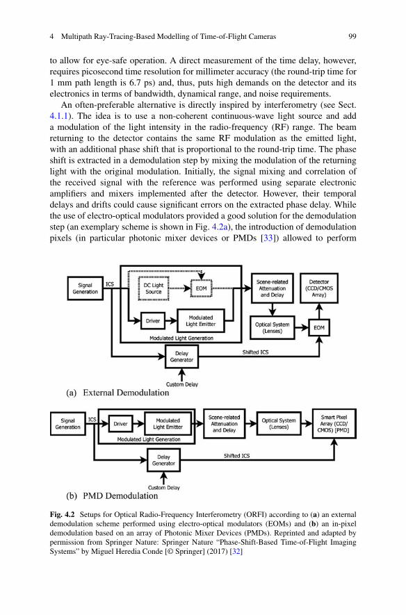
4 Multipath Ray-Tracing-Based Modelling of Time-of-Flight Cameras 99
to allow for eye-safe operation. A direct measurement of the time delay, however,requires picosecond time resolution for millimeter accuracy (the round-trip time for1 mm path length is 6.7 ps) and, thus, puts high demands on the detector and itselectronics in terms of bandwidth, dynamical range, and noise requirements.
An often-preferable alternative is directly inspired by interferometry (see Sect.4.1.1). The idea is to use a non-coherent continuous-wave light source and adda modulation of the light intensity in the radio-frequency (RF) range. The beamreturning to the detector contains the same RF modulation as the emitted light,with an additional phase shift that is proportional to the round-trip time. The phaseshift is extracted in a demodulation step by mixing the modulation of the returninglight with the original modulation. Initially, the signal mixing and correlation ofthe received signal with the reference was performed using separate electronicamplifiers and mixers implemented after the detector. However, their temporaldelays and drifts could cause significant errors on the extracted phase delay. Whilethe use of electro-optical modulators provided a good solution for the demodulationstep (an exemplary scheme is shown in Fig. 4.2a), the introduction of demodulationpixels (in particular photonic mixer devices or PMDs [33]) allowed to perform
Fig. 4.2 Setups for Optical Radio-Frequency Interferometry (ORFI) according to (a) an externaldemodulation scheme performed using electro-optical modulators (EOMs) and (b) an in-pixeldemodulation based on an array of Photonic Mixer Devices (PMDs). Reprinted and adapted bypermission from Springer Nature: Springer Nature “Phase-Shift-Based Time-of-Flight ImagingSystems” by Miguel Heredia Conde [© Springer] (2017) [32]

100 M. Baumgart et al.
the mixing directly at the detector, with a significant increase in detection speedand decrease in detector size, and without the need of an additional demodulationelement in the beam path (Fig. 4.2b). This technique is known as correlation-based ToF (c-ToF) or optical RF interferometry (ORFI) [34], and is at the basisof the modern detection schemes of most lidar and Time-of-Flight devices. Asthe second name suggests, it can be considered an interferometric method, wherethe frequency information is shifted from the frequency of the light to the RFmodulation applied to it. As for interferometry, the detection of the round-triptime reduces to a correlation measurement between an electrical signal containingthe original modulation (control signal) and the modulation of the returning light.Many different implementations exist, for both homodyne and heterodyne detectionschemes, using continuous or discontinuous modulation waveforms.
Here, we will focus on the basics of homodyne-detected amplitude-modulated(AM) c-ToF, which is similar to phase-measuring interferometry [35]. In such ascheme, the brightness of the light source is modulated as a function of time with amodulation frequency fmod in the RF range. Since the frequency of the returninglight coincides with the frequency of the control signal, the information on thedistance difference is coded into the phase-difference ϕ between emitted andreturning wave. In fact, known fmod, determining ϕ is equivalent to determiningthe round-trip time τ and, therefore, the travelled distance D:
ϕ = 2πfmodτ = 2πfmodD
2c(4.2)
where the factor 2 accounts for the fact that the round-trip distance is twice thedistance between the sensor and the scene. It follows that the maximum range Dmaxthat can be measured without ambiguity is
Dmax = c
2fmod(4.3)
and that phase-wrapping projects distances D > Dmax back to this range. Typicalmodulation profiles are sinusoidal or on/off cycles. Demodulation can be achievedby measuring the cross-correlation function between the emitted modulation q(t) (ora control signal which contains the same frequency information) and the modulationof the returning light r(t) at several well-defined time delays t′:
cq,r
(t ′) = lim
T →∞1
2T
∫ T
−T
q∗(t) r(t − t ′
)dt (4.4)
For sinusoidal modulation of the form q(t) = Aq
0 + Aq cos (ω t − ϕ), the cross-correlation function reduces to the form
cq,r
(t ′) = A
q
0Ar0 + AqAr
2cos
(ω t ′ − ϕ
)(4.5)
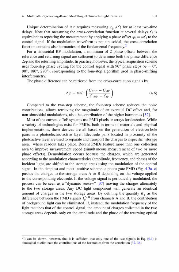
4 Multipath Ray-Tracing-Based Modelling of Time-of-Flight Cameras 101
Unique determination of ϕ requires measuring cq, r(t′) for at least two-timedelays. Note that measuring the cross-correlation function at several delays t′i isequivalent to repeating the measurement by applying a phase offset ϕi = ωt′i to thecontrol signal. If the modulation waveform is not sinusoidal, the cross-correlationfunction contains also harmonics of the fundamental frequency.2
For a sinusoidal RF modulation, a minimum of 2 phase offsets between thereference and returning signal are sufficient to determine both the phase differenceϕ and the returning amplitude. In practice, however, the typical acquisition schemeuses four-step phase cycling for the control signal with 90◦ phase steps (ϕ = 0◦,90◦, 180◦, 270◦), corresponding to the four-step algorithm used in phase-shiftinginterferometry.
The phase difference can be retrieved from the cross-correlation signals by
ϕ = tan-1(
C270◦ − C90◦
C180◦ − C0◦
)(4.6)
Compared to the two-step scheme, the four-step scheme reduces the noisecontributions, allows retrieving the magnitude of an eventual DC offset and, fornon-sinusoidal modulations, also the contribution of the higher harmonics [32].
Most of the current c-ToF systems use PMD pixels or arrays for detection. Whilea variety of technologies exist for PMDs, both in terms of materials and physicalimplementations, these devices are all based on the generation of electron-holepairs in a photoelectric-active layer. Electrode pairs located in proximity of thephotoactive layer are used to separate and transport the charges to a specific “storagearea,” where readout takes place. Recent PMDs feature more than one collectionarea to improve measurement speed (simultaneous measurement of two or morephase offsets). Demodulation occurs because the charges, which are generatedaccording to the modulation characteristics (amplitude, frequency, and phase) of theincident light, are shifted to the storage areas using the modulation of the controlsignal. In the simplest and most intuitive scheme, a photo-gate PMD (Fig. 4.3a–c)pushes the charges to the storage areas A or B depending on the voltage appliedto the corresponding electrode. If the voltage signal is periodically modulated, theprocess can be seen as a “dynamic seesaw” [37] moving the charges alternatelyto the two storage areas. Any DC light component will generate an identicalamount of charges in the two storage areas. By defining the quantity Kϕ as thedifference between the PMD signals IA,B
ϕ from channels A and B, the contributionof background light can be eliminated. If, instead, the modulation frequency of thelight matches that of the control signal, the amount of charges collected in the twostorage areas depends only on the amplitude and the phase of the returning optical
2It can be shown, however, that it is sufficient that only one of the two signals in Eq. (4.4) issinusoidal to eliminate the contributions of the harmonics from the correlation [32, 36].
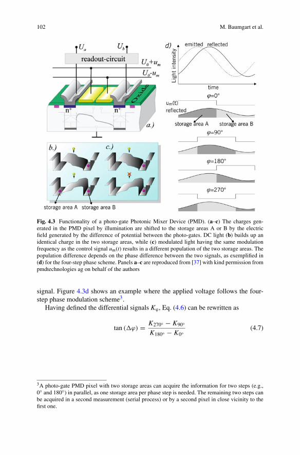
102 M. Baumgart et al.
Fig. 4.3 Functionality of a photo-gate Photonic Mixer Device (PMD). (a–c) The charges gen-erated in the PMD pixel by illumination are shifted to the storage areas A or B by the electricfield generated by the difference of potential between the photo-gates. DC light (b) builds up anidentical charge in the two storage areas, while (c) modulated light having the same modulationfrequency as the control signal um(t) results in a different population of the two storage areas. Thepopulation difference depends on the phase difference between the two signals, as exemplified in(d) for the four-step phase scheme. Panels a–c are reproduced from [37] with kind permission frompmdtechnologies ag on behalf of the authors
signal. Figure 4.3d shows an example where the applied voltage follows the four-step phase modulation scheme3.
Having defined the differential signals Kϕ, Eq. (4.6) can be rewritten as
tan (ϕ) = K270◦ − K90◦
K180◦ − K0◦(4.7)
3A photo-gate PMD pixel with two storage areas can acquire the information for two steps (e.g.,0◦ and 180◦) in parallel, as one storage area per phase step is needed. The remaining two steps canbe acquired in a second measurement (serial process) or by a second pixel in close vicinity to thefirst one.
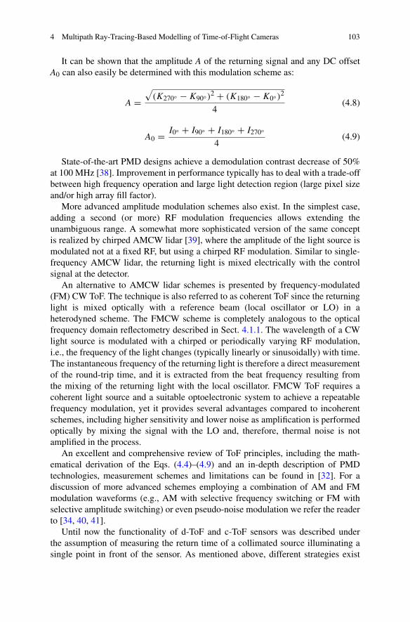
4 Multipath Ray-Tracing-Based Modelling of Time-of-Flight Cameras 103
It can be shown that the amplitude A of the returning signal and any DC offsetA0 can also easily be determined with this modulation scheme as:
A =√
(K270◦ − K90◦)2 + (K180◦ − K0◦)2
4(4.8)
A0 = I0◦ + I90◦ + I180◦ + I270◦
4(4.9)
State-of-the-art PMD designs achieve a demodulation contrast decrease of 50%at 100 MHz [38]. Improvement in performance typically has to deal with a trade-offbetween high frequency operation and large light detection region (large pixel sizeand/or high array fill factor).
More advanced amplitude modulation schemes also exist. In the simplest case,adding a second (or more) RF modulation frequencies allows extending theunambiguous range. A somewhat more sophisticated version of the same conceptis realized by chirped AMCW lidar [39], where the amplitude of the light source ismodulated not at a fixed RF, but using a chirped RF modulation. Similar to single-frequency AMCW lidar, the returning light is mixed electrically with the controlsignal at the detector.
An alternative to AMCW lidar schemes is presented by frequency-modulated(FM) CW ToF. The technique is also referred to as coherent ToF since the returninglight is mixed optically with a reference beam (local oscillator or LO) in aheterodyned scheme. The FMCW scheme is completely analogous to the opticalfrequency domain reflectometry described in Sect. 4.1.1. The wavelength of a CWlight source is modulated with a chirped or periodically varying RF modulation,i.e., the frequency of the light changes (typically linearly or sinusoidally) with time.The instantaneous frequency of the returning light is therefore a direct measurementof the round-trip time, and it is extracted from the beat frequency resulting fromthe mixing of the returning light with the local oscillator. FMCW ToF requires acoherent light source and a suitable optoelectronic system to achieve a repeatablefrequency modulation, yet it provides several advantages compared to incoherentschemes, including higher sensitivity and lower noise as amplification is performedoptically by mixing the signal with the LO and, therefore, thermal noise is notamplified in the process.
An excellent and comprehensive review of ToF principles, including the math-ematical derivation of the Eqs. (4.4)–(4.9) and an in-depth description of PMDtechnologies, measurement schemes and limitations can be found in [32]. For adiscussion of more advanced schemes employing a combination of AM and FMmodulation waveforms (e.g., AM with selective frequency switching or FM withselective amplitude switching) or even pseudo-noise modulation we refer the readerto [34, 40, 41].
Until now the functionality of d-ToF and c-ToF sensors was described underthe assumption of measuring the return time of a collimated source illuminating asingle point in front of the sensor. As mentioned above, different strategies exist
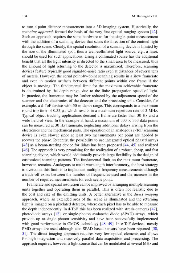
104 M. Baumgart et al.
to turn a point distance measurement into a 3D imaging system. Historically, thescanning approach formed the basis of the very first optical ranging system [42].Such an approach requires the same hardware as for the single-point measurementwith the addition of a scanning device that scans the direction of the emitted lightthrough the scene. Clearly, the spatial resolution of a scanning device is limited bythe size of the illuminated spot, thus a well-collimated light source, e.g., a laser,should be used for such applications. Using a collimated source has the additionalbenefit that all the light intensity is directed to the small area to be measured, thusthe amount of light returning to the detector is maximized. Therefore, scanningdevices feature typically good signal-to-noise ratio even at distances of several tensof meters. However, the serial point-by-point scanning results in a slow framerateand even in motion artifacts between different points within one frame if theobject is moving. The fundamental limit for the maximum achievable framerateis determined by the depth range, due to the finite propagation speed of light.In practice, the framerate may be further reduced by the adjustment speed of thescanner and the electronics of the detector and the processing unit. Consider, forexample, a d-ToF device with 50 m depth range. This corresponds to a maximumround-trip time of 0.33 μs which results in a maximum repetition rate of 3 MHz.Typical object tracking applications demand a framerate faster than 30 Hz and awide field-of-view. In the example at hand, a maximum of 333 × 333 data pointscan be measured at 30 Hz framerate, neglecting additional delays arising from theelectronics and the mechanical parts. The operation of an analogous c-ToF scanningdevice is even slower since at least two measurements per point are needed torecover the phase. Recently, the possibility to use integrated optical phased arrays[43] as a beam-steering device for lidars has been proposed [44, 45] and realized[46]. The approach is very promising for the realization of a robust, cheap, and fastscanning device, which would additionally provide large flexibility in the design ofcustomized scanning patterns. The fundamental limit on the maximum framerate,however, remains. Analogous to multi-wavelength interferometry, the best strategyto overcome this limit is to implement multiple-frequency measurements althougha trade-off exists between the number of frequencies used and the increase in thenumber of required measurements for each scene point.
Framerate and spatial resolution can be improved by arranging multiple scanningunits together and operating them in parallel. This is often not realistic due tothe cost and size of the emitting units. A better alternative is the direct imagingapproach, where an extended area of the scene is illuminated and the returninglight is imaged on a pixelated detector, where each pixel has to be able to measurethe depth independently. In d-ToF, this has been realized with streak-cameras [47],photodiode arrays [12], or single-photon avalanche diode (SPAD) arrays, whichprovide up to single-photon sensitivity and have been successfully implementedwith good performance in CMOS technology [48, 49]. In c-ToF devices, mostlyPMD arrays are used although also SPAD-based sensors have been reported [50,51]. The direct imaging approach requires very few optical elements and allowsfor high integration and massively parallel data acquisition and processing. Theapproach requires, however, a light source that can be modulated at several MHz and
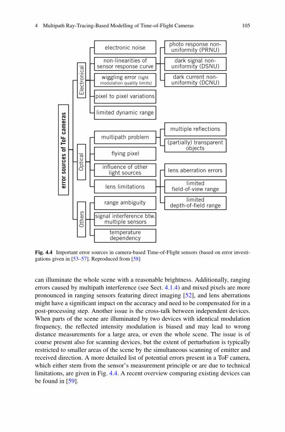
4 Multipath Ray-Tracing-Based Modelling of Time-of-Flight Cameras 105
Fig. 4.4 Important error sources in camera-based Time-of-Flight sensors (based on error investi-gations given in [53–57]. Reproduced from [58]
can illuminate the whole scene with a reasonable brightness. Additionally, rangingerrors caused by multipath interference (see Sect. 4.1.4) and mixed pixels are morepronounced in ranging sensors featuring direct imaging [52], and lens aberrationsmight have a significant impact on the accuracy and need to be compensated for in apost-processing step. Another issue is the cross-talk between independent devices.When parts of the scene are illuminated by two devices with identical modulationfrequency, the reflected intensity modulation is biased and may lead to wrongdistance measurements for a large area, or even the whole scene. The issue is ofcourse present also for scanning devices, but the extent of perturbation is typicallyrestricted to smaller areas of the scene by the simultaneous scanning of emitter andreceived direction. A more detailed list of potential errors present in a ToF camera,which either stem from the sensor’s measurement principle or are due to technicallimitations, are given in Fig. 4.4. A recent overview comparing existing devices canbe found in [59].
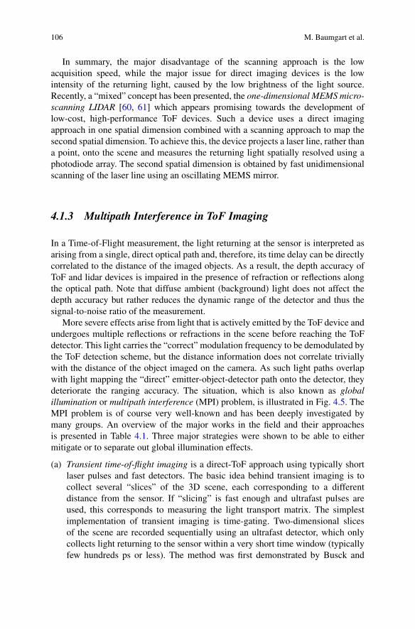
106 M. Baumgart et al.
In summary, the major disadvantage of the scanning approach is the lowacquisition speed, while the major issue for direct imaging devices is the lowintensity of the returning light, caused by the low brightness of the light source.Recently, a “mixed” concept has been presented, the one-dimensional MEMS micro-scanning LIDAR [60, 61] which appears promising towards the development oflow-cost, high-performance ToF devices. Such a device uses a direct imagingapproach in one spatial dimension combined with a scanning approach to map thesecond spatial dimension. To achieve this, the device projects a laser line, rather thana point, onto the scene and measures the returning light spatially resolved using aphotodiode array. The second spatial dimension is obtained by fast unidimensionalscanning of the laser line using an oscillating MEMS mirror.
4.1.3 Multipath Interference in ToF Imaging
In a Time-of-Flight measurement, the light returning at the sensor is interpreted asarising from a single, direct optical path and, therefore, its time delay can be directlycorrelated to the distance of the imaged objects. As a result, the depth accuracy ofToF and lidar devices is impaired in the presence of refraction or reflections alongthe optical path. Note that diffuse ambient (background) light does not affect thedepth accuracy but rather reduces the dynamic range of the detector and thus thesignal-to-noise ratio of the measurement.
More severe effects arise from light that is actively emitted by the ToF device andundergoes multiple reflections or refractions in the scene before reaching the ToFdetector. This light carries the “correct” modulation frequency to be demodulated bythe ToF detection scheme, but the distance information does not correlate triviallywith the distance of the object imaged on the camera. As such light paths overlapwith light mapping the “direct” emitter-object-detector path onto the detector, theydeteriorate the ranging accuracy. The situation, which is also known as globalillumination or multipath interference (MPI) problem, is illustrated in Fig. 4.5. TheMPI problem is of course very well-known and has been deeply investigated bymany groups. An overview of the major works in the field and their approachesis presented in Table 4.1. Three major strategies were shown to be able to eithermitigate or to separate out global illumination effects.
(a) Transient time-of-flight imaging is a direct-ToF approach using typically shortlaser pulses and fast detectors. The basic idea behind transient imaging is tocollect several “slices” of the 3D scene, each corresponding to a differentdistance from the sensor. If “slicing” is fast enough and ultrafast pulses areused, this corresponds to measuring the light transport matrix. The simplestimplementation of transient imaging is time-gating. Two-dimensional slicesof the scene are recorded sequentially using an ultrafast detector, which onlycollects light returning to the sensor within a very short time window (typicallyfew hundreds ps or less). The method was first demonstrated by Busck and
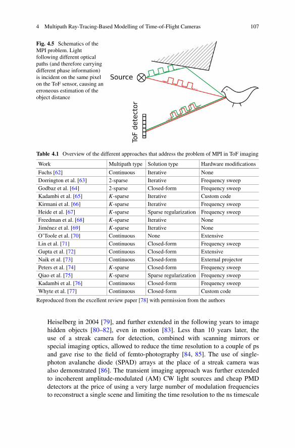
4 Multipath Ray-Tracing-Based Modelling of Time-of-Flight Cameras 107
Fig. 4.5 Schematics of theMPI problem. Lightfollowing different opticalpaths (and therefore carryingdifferent phase information)is incident on the same pixelon the ToF sensor, causing anerroneous estimation of theobject distance
Table 4.1 Overview of the different approaches that address the problem of MPI in ToF imaging
Work Multipath type Solution type Hardware modifications
Fuchs [62] Continuous Iterative NoneDorrington et al. [63] 2-sparse Iterative Frequency sweepGodbaz et al. [64] 2-sparse Closed-form Frequency sweepKadambi et al. [65] K-sparse Iterative Custom codeKirmani et al. [66] K-sparse Iterative Frequency sweepHeide et al. [67] K-sparse Sparse regularization Frequency sweepFreedman et al. [68] K-sparse Iterative NoneJiménez et al. [69] K-sparse Iterative NoneO’Toole et al. [70] Continuous None ExtensiveLin et al. [71] Continuous Closed-form Frequency sweepGupta et al. [72] Continuous Closed-form ExtensiveNaik et al. [73] Continuous Closed-form External projectorPeters et al. [74] K-sparse Closed-form Frequency sweepQiao et al. [75] K-sparse Sparse regularization Frequency sweepKadambi et al. [76] Continuous Closed-form Frequency sweepWhyte et al. [77] Continuous Closed-form Custom code
Reproduced from the excellent review paper [78] with permission from the authors
Heiselberg in 2004 [79], and further extended in the following years to imagehidden objects [80–82], even in motion [83]. Less than 10 years later, theuse of a streak camera for detection, combined with scanning mirrors orspecial imaging optics, allowed to reduce the time resolution to a couple of psand gave rise to the field of femto-photography [84, 85]. The use of single-photon avalanche diode (SPAD) arrays at the place of a streak camera wasalso demonstrated [86]. The transient imaging approach was further extendedto incoherent amplitude-modulated (AM) CW light sources and cheap PMDdetectors at the price of using a very large number of modulation frequenciesto reconstruct a single scene and limiting the time resolution to the ns timescale
108 M. Baumgart et al.
[67]. Thanks to the “slicing” approach and the very short capture times, transientimaging devices allow to see through highly scattering media, including fog andsmoke, and even through flames and other bright media [87]. Recent advances inthe technology of avalanche photodiode arrays form the basis of the novel long-range ToF sensor presented in 2018 by Panasonic Corporation, which showeddetection up to 250 m at night [88, 89].
(b) Multipath interference correction: For typical c-ToF acquisition schemes, theinversion of the phase signal to reconstruct the distance information is an ill-posed problem in the presence of MPI. A lot of approaches and algorithmshave been proposed to mitigate the ranging errors caused by MPI effects onToF devices. Typically, the problem is addressed from two perspectives: theMPI is either corrected by post-processing algorithms, or its contribution isseparated from the direct-path reflections using clever measurement schemesand/or specific hardware implementations. In general, pure post-processingstrategies [62, 90, 91] show limited applicability because of the large variabilityof MPI contributions in real-world scenarios. Nevertheless, very recently apost-processing correction algorithm based on a convolutional neural networkdemonstrated a reliable correction for MPI effects on several scenes, with acorrection time of about 10 ms per frame [92]. Mixed methods, employingspecific mathematical description of the light transport to identify strategiescapable of separating MPI contributions, have shown more success. Whileinitial works imposed strict conditions for the scene to be modelled [62, 91],recent approaches focused on more generalized formulations, which are mostlybased on either sparsity or compressibility of light transport in the time domainand typically exploit measurements with several modulation frequencies [63,93]. Sparse models are, however, not accurate in the presence of scatteringmedia. Nevertheless, a recent novel approach based on convolutional sparsecoding showed a very good performance through scattering media, albeit atthe price of acquiring a large set of data for reconstructing the image [94]. Analternative approach focuses on the fact that the time-domain light transport canbe described and analyzed in the frequency domain without loss of information.This is the basic principle behind the Phasor Imaging Approach proposedby Gupta and coworkers [72], which relies on the observation that, for mostscenes and global illumination circumstances, there is a threshold modulationfrequency such that at higher frequencies the global illumination componentdoes not act on the phase of the returning light, but only appears as a constantoffset. This allows reconstruction of a scene by measuring the full range atlow frequencies and then removing MPI contributions using high modulationfrequencies. A more detailed review of such approaches is given in the recentpaper of Jarabo and coworkers [78].
(c) Coded light: By operating a ToF device with the addition of clever temporalor spatio-temporal modulation sequences, multipath interference effects canbe separated or “filtered out.” Among the most relevant examples, adding aspatial modulation to the temporal modulation makes it possible to analyzeand retrieve 3D scenes more accurately in the presence of global illumination
4 Multipath Ray-Tracing-Based Modelling of Time-of-Flight Cameras 109
effects [70, 73]. For 1D-scanning devices, epipolar imaging projecting laserlines on the scene also show some improvement in terms of reduction of globalillumination artifacts [95]. Another possibility is to use specific temporal pulsesequences to selectively reconstruct the 3D scene. For example, Kadambi andcoworkers showed that, by using customized temporal coding, a functionalityanalogous to that of time-gating d-ToF cameras can be achieved, i.e., the scenecan be “sliced” in 2D images corresponding to different distances [65]. Ingeneral, coded-light approaches are very promising due to their typical low-cost applicability, but they usually require a few seconds to fully reconstruct ascene.
4.1.4 Simulation Frameworks for ToF Devices
The typical computer graphics rendering pipeline for 3D scenes already brings partsof the functionality needed for a ToF camera simulator. It takes 3D data (camera,objects, surfaces, textures, and light sources) as input and generates a 2D imagewith brightness per pixel and/or color values. In recent years, a lot of progress interms of algorithm development and processing speed was achieved in the fieldof physical based rendering (PBS). A comprehensive review with accompanyingsource code for many example scenes is available on this topic [96]. In this context“physical”—sometimes also referred to as “predictive”—means that rendering ofa scene is performed using light interactions on surfaces and in the bulk materialthat are based on optical models rather than using algorithms which aim to givea visually convincing effect (“plausible” or “visually rich” rendering). Such anapproach naturally allows including the effects of global illumination. There areseveral ray-tracing-based strategies to model global illumination. According to [97],the following methods are most widely used:
• Path tracing: Monte Carlo rays are sent from the eye to scene objects.• Photon tracing: Monte Carlo rays are sent from light source(s) to scene objects.• Bidirectional path tracing: Path and photon tracing is performed and match-
making between partial paths from each direction is applied to get full light-to-eye paths.
• Metropolis: The initial set of seeds is taken from any of the above-mentionedmethods (bidirectional is most popular). Then some slight modifications to theexisting paths are applied. Thus, nearby paths, which are difficult to find, canbe detected with a lower number of rays. This method uses the Metropolisalgorithm, which is a special implementation of the Monte-Carlo concept, toperform ray seeding and weighting for the overall brightness calculation.
• Radiosity: A full finite element solution is performed, and the results areprojected to the screen.
Such renderers are very suited to simulate realistic brightness (intensity) dis-tributions, but—to our knowledge—lack the ability to calculate the average path
110 M. Baumgart et al.
length per pixel. In contrast to rasterization rendering methods4, ray-tracing-basedrendering methods calculate ray–object intersections making them the ideal basefor ToF camera simulations. Several strategies of different complexity exist todetermine the path length between the ToF camera and the objects in the scene.The simplest approach consists in using a set of test rays launched from the sensorposition. This approach uses the implicit assumption that a light source is locatedat the position of each detector pixel to justify reverse ray-tracing from the detectortowards the scene. Collision detection algorithms are used to check if and whichsurfaces are located in the direction of a test ray. The intersection coordinates areused to calculate the length of the corresponding test ray. The scene might be definedby several surfaces, where one is placed behind another. Thus, the length calculationhas to be repeated for every surface which intersects with the test ray. The shortestdistance, which belongs to the closest and thus non-occluded surface, is taken asthe valid value. This procedure is repeated for every test ray. Pre-filtering strategiesof possible occluded surfaces allow (further) reduction of the calculation time. Thisprocedure only accounts for direct “line-of-sight” distances and ignores reflectionand scattering of light between surfaces. Various ToF simulators, like ROS/Gazebo[98, 99] or PMDSim [100, 101], implement this nearest objects distances detection.
The Blensor [102] algorithm, which is based on the Blender engine, enhancesthis method for rudimentary support of optical properties of surfaces and objects.If a test ray intersects with a surface exhibiting specular reflective (mirror-like)properties, the ray is rotated at the intersection according to the law of reflection andcollision detection is performed again for the new direction. The total path lengthis then the sum of the individual segments. This is repeated until the ray intersectswith a diffusively reflecting surface or reaches a predefined maximum length. Thesecond case leads to an invalid ray. In the first case, a valid ray is returned with atotal length as the sum of all individual segments as described above while keepingthe original direction of the ray (i.e., the direction from the pixel coordinate onthe sensor through the focal point of the ToF camera). Artifacts in depth arisingfrom mirror-like reflective surfaces can thus be simulated. Blensor currently doesnot support transmission with refraction and true multipath analysis for realisticsurfaces and objects (with partial reflectance and transmittance). Another approachhas been developed, based on the MatLab platform, which can distinguish betweenthe direct and global component of scenes with reflective surfaces [72].
The most advanced ToF camera simulator—to our knowledge—is the CamSimtoolbox [103]. It is a framework for evaluating ToF camera performance usingOpenGL as backend for 3D scene creation and rendering and supports amplitude-modulated continuous-wave Time-of-Flight cameras with 4 phase images. It fea-tures an arbitrary number of light sources, even with measured intensity distribution
4In rasterization rendering methods, scene objects are created from a mesh of virtual trianglesor polygons. Then, this mesh is projected onto a 2D screen and pixelated. The result is the 2Dimage of the 3D scene. This approach is typically computational less demanding than ray-tracingapproaches.

4 Multipath Ray-Tracing-Based Modelling of Time-of-Flight Cameras 111
and structured light, and a large number of surface properties for the objects in thescene, includes lens distortions and vignetting, and allows modelling simple anima-tion effects. The illumination model even enables rudimentary global illuminationeffects with “single-bounce indirect illumination via reflective shadow maps” [104].Unfortunately, CamSim only supports surface interaction effects and, thus, ignoresrefraction.
4.2 Description of the Simulation Procedure
Applications for ranging cameras can be found in the fields of enhanced reality[105], robotics [106, 107], healthcare [108, 109], and autonomous mobility, both tomonitor the alertness of the driver [110, 111] and the vehicle surrounding.
Despite their great potential, active ranging cameras face several challenges withrespect to safe and reliable operation in outdoor scenarios. In particular:
• the necessity to monitor a large area on very short time scales, which requireseither fast scanning techniques or very sensitive detectors for direct imagingimplementations
• the presence of background illumination, which reduces the dynamic range ofthe sensor
• the capability to detect objects with very different surface properties (e.g., semi-transparent, highly absorbing, highly reflecting)
• the need to maintain good performance in challenging environmental conditionssuch as rain, snow, or fog.
For an efficient development of technology best equipped to deal with thesechallenges, it is necessary to develop simulation approaches capable of predictingthe performance of different technologies. Ideally, these simulation approaches canreliably model objects with very different optical properties as well as differentenvironmental conditions and can simultaneously return not only the extent of theranging perturbation as measured by the sensor, but also a precise evaluation ofthe origin of such error. Finally, the approach must also allow for a quantitativecomparison between different hardware and technologies.
This chapter presents a simulation approach for ToF cameras based on ZemaxOpticStudio
®and Python that attempts to fulfil such goals. The current implemen-
tation is limited to direct imaging ToF cameras but can easily be extended to includeLIDAR scanning schemes. The application of our approach to different objects andenvironmental conditions will be presented in Sects. 4.3 and 4.4, while Sect. 4.5will focus on a detailed comparison of our approach with existing ToF simulationalgorithms including a discussion of the advantages and drawbacks of our approach.
112 M. Baumgart et al.
4.2.1 The Simulation Approach and Its Implementation
The simulation approach we present here is based on a two-step strategy. In the firststep (simulation phase), a steady-state ray-tracing simulation is run for the modelToF sensor in front of an arbitrary scene. Within the simulation phase, the intensityand the full optical path of each ray reaching the ToF detector are recorded includingthe details of all ray segments and all the interactions that took place within the ToFoptics or within the scene. The master parameter for all the following evaluations ofthe ToF signal is the optical path length (OPL), defined as
OPL =∑
i
nidi (4.10)
where di is the geometrical length of the ith ray segment, ni is the refractive indexof the medium in which the ith ray segment propagates and the sum runs over allthe ray segments from the source to the detector. Given the OPL, using the speed oflight c, the travel time t of each ray can be reconstructed as t = OPL/c.
The simulation phase is performed with Zemax OpticStudio®
(ZOS). ZOS isa development software for optical system design supporting Monte Carlo methodsfor ray-tracing. Multiple light sources, 3D objects and detectors can be placed withinthe 3D scene. The software allows defining the optical properties independentlyfor each surface (transmission, absorption, reflectivity, and scattering) and volume(refractive index, volumetric scattering). Additionally, the ray-tracing kernel keepstrack of the absolute energy values of each ray at the ray-segment level and canaccount for polarization (each ray is split into its electric and magnetic field vectors),enabling, for example, the calculation of the surface reflectance from the object’sindex of refraction without any further assumption. Rays hitting a certain object ordetector can be stored and saved with their intensity and their complete ray path,including information on the occurrence and position of reflection and/or scatteringevents. The possibility to simulate all optical effects (at least within the geometricoptics model) and the built-in functionality of ray-segment fine data storage makeZOS an ideal choice for ToF ray-tracing simulations. Nevertheless, the completeprocedure, as shown in Fig. 4.6 and described in the following chapters, is valid forany ray-tracing-based simulation software as long as the OPL of each ray can bestored or extracted.
It’s important to note that the method presented here does not support real-timesimulation of the ToF scene since the simulation is based on steady-state ray-tracing.Effects arising from moving objects and time-dependent scenes can be modelledby performing a simulation sequence, where the position of certain objects in thescene is systematically varied; however, the procedure can be slow due to thecomputational time required by the individual simulations.
The second step (processing phase) deals with post-processing of the ray-tracingresults and reconstruction of the full 3D point-cloud. The steps described here,which are presented in Fig. 4.6, only deal with the reconstruction of the 3D point-
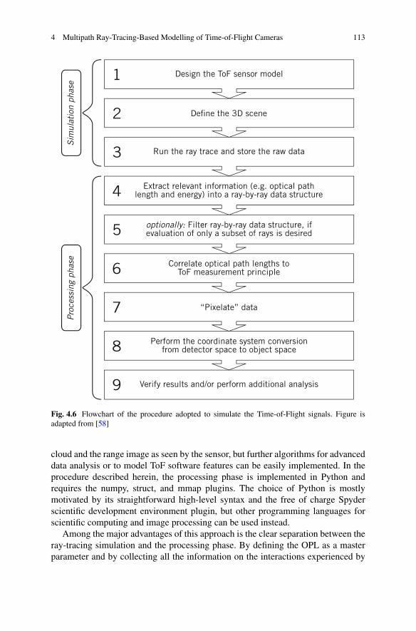
4 Multipath Ray-Tracing-Based Modelling of Time-of-Flight Cameras 113
Fig. 4.6 Flowchart of the procedure adopted to simulate the Time-of-Flight signals. Figure isadapted from [58]
cloud and the range image as seen by the sensor, but further algorithms for advanceddata analysis or to model ToF software features can be easily implemented. In theprocedure described herein, the processing phase is implemented in Python andrequires the numpy, struct, and mmap plugins. The choice of Python is mostlymotivated by its straightforward high-level syntax and the free of charge Spyderscientific development environment plugin, but other programming languages forscientific computing and image processing can be used instead.
Among the major advantages of this approach is the clear separation between theray-tracing simulation and the processing phase. By defining the OPL as a masterparameter and by collecting all the information on the interactions experienced by
114 M. Baumgart et al.
each ray, different hardware implementations of ToF cameras, frequency analysisfor correlation-based ToF, or an analysis of the influence of certain ray paths onthe total reconstructed 3D point-cloud can be individually and systematically testedwith the same simulation data. In particular, this allows for efficient systematictesting of the performance of different ToF hardware (or software) for different“risk” scenarios or perturbation elements.
Below, each passage of the simulation and processing phases is described in moredetails.
4.2.1.1 Simulation Phase
ToF Camera and 3D Scenery Creation
The ToF camera model comprises a light source, a two-dimensional pixelated (andabsorbing) detector array, and imaging optics. The light source type can be chosenfrom a list of supported sources, which are based on mathematical models and aredefined by parameters determining their spatial extension and the characteristicsof the emitted light distribution. Alternatively, measured or user-defined lightdistributions can be used as a ray source. The software allows to define multiplelight sources (including ambient light source models) and, of course, to distinguishrays originating from different sources. Optical elements like lenses and objectivescan be either imported in ZOS using the parameters provided by the manufacturer ormodelled using the respective object types supported by ZOS. While the first optionis recommended when testing the performances of a well-known system, the secondoption is suitable for optimization of the optical system of interest, due to the widecustomization possibilities. Besides lenses and objectives, ZOS supports numerousinternal 3D object types like cubes and spheres that can be used to model a ToFscene, but it can also operate on imported CAD scenes or on a mixture of both. Inboth cases, the properties of all object surfaces can be defined independently. As asmall drawback, the light source(s) always have to be placed separately and cannotbe imported as part of a CAD file.
Ray-Tracing and List of Rays Containing Detector Coordinates, Intensity, andOPL
The ray parameters are typically created with a rigorous random or a Sobol-basedpseudo-random algorithm. Alternatively, a regular grid or a user-defined distributionof rays can be used.
Upon ray-tracing, a ray-trace raw data file is generated, including energy andoptical path length information for each ray and on a ray-segment to ray-segmentlevel. In particular, not only the length of each ray segment but also the coordinatesof each interaction are stored, including the coordinates where the ray hits the
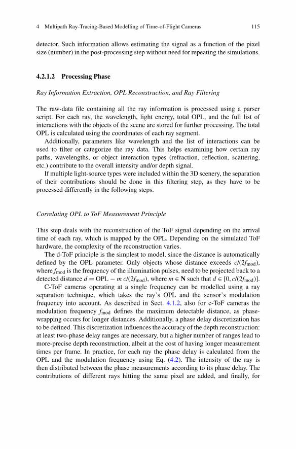
4 Multipath Ray-Tracing-Based Modelling of Time-of-Flight Cameras 115
detector. Such information allows estimating the signal as a function of the pixelsize (number) in the post-processing step without need for repeating the simulations.
4.2.1.2 Processing Phase
Ray Information Extraction, OPL Reconstruction, and Ray Filtering
The raw-data file containing all the ray information is processed using a parserscript. For each ray, the wavelength, light energy, total OPL, and the full list ofinteractions with the objects of the scene are stored for further processing. The totalOPL is calculated using the coordinates of each ray segment.
Additionally, parameters like wavelength and the list of interactions can beused to filter or categorize the ray data. This helps examining how certain raypaths, wavelengths, or object interaction types (refraction, reflection, scattering,etc.) contribute to the overall intensity and/or depth signal.
If multiple light-source types were included within the 3D scenery, the separationof their contributions should be done in this filtering step, as they have to beprocessed differently in the following steps.
Correlating OPL to ToF Measurement Principle
This step deals with the reconstruction of the ToF signal depending on the arrivaltime of each ray, which is mapped by the OPL. Depending on the simulated ToFhardware, the complexity of the reconstruction varies.
The d-ToF principle is the simplest to model, since the distance is automaticallydefined by the OPL parameter. Only objects whose distance exceeds c/(2fmod),where fmod is the frequency of the illumination pulses, need to be projected back to adetected distance d = OPL − m c/(2fmod), where m ∈ N such that d ∈ [0, c/(2fmod)].
C-ToF cameras operating at a single frequency can be modelled using a rayseparation technique, which takes the ray’s OPL and the sensor’s modulationfrequency into account. As described in Sect. 4.1.2, also for c-ToF cameras themodulation frequency fmod defines the maximum detectable distance, as phase-wrapping occurs for longer distances. Additionally, a phase delay discretization hasto be defined. This discretization influences the accuracy of the depth reconstruction:at least two-phase delay ranges are necessary, but a higher number of ranges lead tomore-precise depth reconstruction, albeit at the cost of having longer measurementtimes per frame. In practice, for each ray the phase delay is calculated from theOPL and the modulation frequency using Eq. (4.2). The intensity of the ray isthen distributed between the phase measurements according to its phase delay. Thecontributions of different rays hitting the same pixel are added, and finally, for
116 M. Baumgart et al.
the widespread four-phase scheme, the distance signal is calculated according toEq. (4.7). Note that this procedure inherently assumes a rectangular modulationwaveform for both control and returning signals.
Multi-frequency c-ToF sensors are interesting as they can partially overcome thelimitation of the modulation-frequency bound measurement range and, to someextent, can also limit the influence of global illumination on the ToF rangingaccuracy [52]. Such sensors can be modelled via repeating the procedure of thesingle-frequency ToF for every frequency.
Pixelate Data
This step mimics the functionality of a pixelated detector. Accordingly, the detectorarea is divided in a pixel matrix, and the ray information for all rays arriving onthe detector within a certain pixel area is combined. Optionally, the space betweenpixels can be also accounted for by eliminating the rays arriving on such gaps fromthe following analysis.
As a result, the ray-based path length and intensity information is converted intoa matrix-like pattern for a given number of horizontal and vertical sensor pixelsin this discretization process. In the simplest case (no multi-frequency sensor, nodirect vs. global illumination differentiation), this procedure returns two matrices.The first matrix contains the integrated intensity at each pixel, which is the sum ofthe intensities of all rays arriving at each pixel. The second matrix contains theaverage path length. For each pixel, the latter is obtained as the average of theOPLs of each ray impinging on the pixel, weighted by the ray intensity. Differentsmoothing strategies, where the ray data also contributes to neighboring pixels, canbe introduced within this step.
Coordinate System Conversion
Finally, a coordinate system conversion from the image space (defined in pixel units)to the object space is necessary. The behavior of the modelled imaging objective hasto be taken into account to properly perform this conversion. The simplest approachto define such a camera function is to use a global magnification factor for all x- andy-coordinates (pinhole camera). This gives a first approximation of the 3D scene.This approach does not take into account magnification changes due to defocusingand lens aberration effects for objects at different lateral and axial positions. Tothat end, more complex coordinate mapping and calibration approaches can alsobe implemented. For a detailed description of such mapping functions and theirimplementation, we refer the reader to [112–114].
4 Multipath Ray-Tracing-Based Modelling of Time-of-Flight Cameras 117
4.3 Simulation Results of a ToF Camera Observing a TestScene
In this section, we present the simulation of a ToF camera in front of a simple scenefollowing our approach. In particular, we will focus on some key advantages of thismethod, such as the capability of filtering and analyzing single ray paths and thepossibility of modelling different ToF hardware without having to re-trace the scene.This allows for a quick and direct comparison between different ToF technologies.
The same ToF model and the same test scene described in this section will beused in the next chapters to demonstrate the capabilities of our approach in thepresence of refracting and scattering media.
4.3.1 Simulation Setup
The simulation setup, shown in Fig. 4.7, consists of a model of the ToF camera anda scene located in front of it. Please note that all 3D plots shown in this publicationuse parallel projection for the 3D effect.
The ToF camera model comprises a monochromatic point source at 850 nm witha Gaussian angular intensity distribution (18◦ full angle divergence @ 1/e2). Thetotal power of the light source is set to 1 W. Alternatively, a source array can beused. A Petzval lens design (see inset in Fig. 4.7) was chosen for the receiveroptics because this lens type offers good light collection efficiency. An antireflective
Fig. 4.7 Model for the ToF sensor and a simple scene. The sensor consists of a point source anda pixelated detector array preceded by a Petzval lens optics. The scene consists of four cubes withdiffuse-scattering surfaces. Figure is adapted from [3]
118 M. Baumgart et al.
coating optimized for 850 nm was applied on the lens surfaces. The ToF sensor isdescribed by a pixelated absorptive detector. Since the outcome of the simulation isgiven by the coordinates of each ray at the detector, the number of detector pixels inthe simulation can be kept low.
The scene itself consists of four cubes of different sizes, located at distancesbetween 1.8 and 2.5 m from the ToF camera and forming different angles withrespect to it. For the examples shown here, the cubes have identical surfaceproperties, as this allows investigating the effect of different orientations of thescene on the ToF reconstruction. The surface of the cubes is chosen to be partlyabsorbing (90%) and partly scattering (10%). The scattering distribution is modelledas Gaussian, with a Bi-Directional Scatter Distribution Function (BSDF) defined as:
BSDF(−→
x) = A exp
(−∣∣−→x ∣∣2σ 2
)(4.11)
where the vector −→x is the difference between the projection of the specular ray
vector and the scattered ray vector onto the surface plane, σ is the standard deviationof the Gaussian distribution on the projected plane (σ = 1 in our case), and A is anormalization factor. While changes in the BSDF function can only be investigatedby running a new simulation, the percentage of absorption and scattering from eachsurface can be addressed in the processing phase and its effect can be investigatedwithout repeating the ray-tracing simulation phase.
4.3.2 Scene Reconstruction Using Ray-Tracing Data
The scene reconstruction is performed as described in Sect. 4.2.1.2. The recon-struction results (intensity and distance as seen by the ToF sensor) are shown inFigs. 4.8a, b. Figure 4.8c plots the full data point-cloud. The ground-truth objectpositions are shown as grey shades. The coordinate transformation from imagespace to object space is performed assuming a constant global magnification factorfor all x- and y-coordinates. Therefore, lens aberration errors stemming from thePetzval lens can easily be observed in the reconstructed 3D plot. The differenceswith the ground-truth values can be minimized by taking into account the exact lensfunction. This advanced correction was not implemented since it has little impactfor the examples presented here, where mostly the influence of adverse ambientconditions on the ranging accuracy is evaluated.
As the antireflective lens coating cannot suppress all reflections, the remainingreflections can be seen as noise in the outer areas of the imaged scene (Fig. 4.8c).The magnitude of such reflections is so low that it has no significance for a real ToF
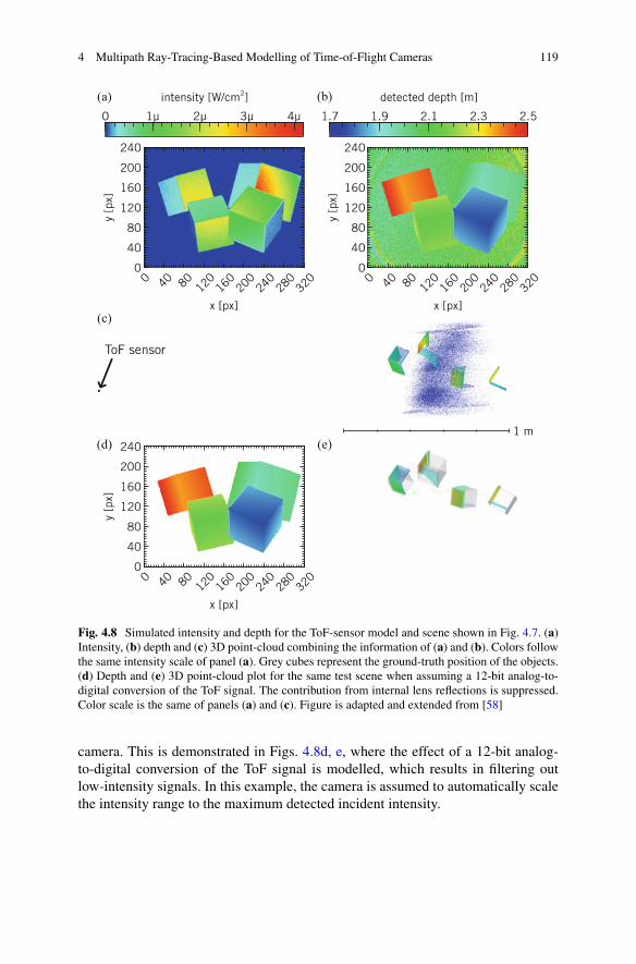
4 Multipath Ray-Tracing-Based Modelling of Time-of-Flight Cameras 119
Fig. 4.8 Simulated intensity and depth for the ToF-sensor model and scene shown in Fig. 4.7. (a)Intensity, (b) depth and (c) 3D point-cloud combining the information of (a) and (b). Colors followthe same intensity scale of panel (a). Grey cubes represent the ground-truth position of the objects.(d) Depth and (e) 3D point-cloud plot for the same test scene when assuming a 12-bit analog-to-digital conversion of the ToF signal. The contribution from internal lens reflections is suppressed.Color scale is the same of panels (a) and (c). Figure is adapted and extended from [58]
camera. This is demonstrated in Figs. 4.8d, e, where the effect of a 12-bit analog-to-digital conversion of the ToF signal is modelled, which results in filtering outlow-intensity signals. In this example, the camera is assumed to automatically scalethe intensity range to the maximum detected incident intensity.
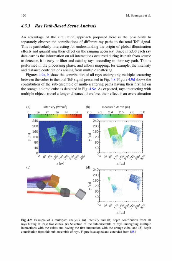
120 M. Baumgart et al.
4.3.3 Ray Path-Based Scene Analysis
An advantage of the simulation approach proposed here is the possibility toseparately observe the contributions of different ray paths to the total ToF signal.This is particularly interesting for understanding the origin of global illuminationeffects and quantifying their effect on the ranging accuracy. Since in ZOS each raydata carries the information on all interactions occurred during its path from sourceto detector, it is easy to filter and catalog rays according to their ray path. This isperformed in the processing phase, and allows mapping, for example, the intensityand distance contributions arising from multiple scattering.
Figures 4.9a, b show the contribution of all rays undergoing multiple scatteringbetween the cubes to the total ToF signal presented in Fig. 4.8. Figure 4.9d shows thecontribution of the sub-ensemble of multi-scattering paths having their first hit onthe orange-colored cube as depicted in Fig. 4.9c. As expected, rays interacting withmultiple objects travel a longer distance; therefore, their effect is an overestimation
Fig. 4.9 Example of a multipath analysis. (a) Intensity and (b) depth contribution from allrays hitting at least two cubes. (c) Selection of the sub-ensemble of rays undergoing multipleinteractions with the cubes and having the first interaction with the orange cube, and (d) depthcontribution from this sub-ensemble of rays. Figure is adapted and extended from [58]
4 Multipath Ray-Tracing-Based Modelling of Time-of-Flight Cameras 121
of the camera-scene distance. However, as can be seen by comparing Fig. 4.9a withFig. 4.8a, multipath contributions remain two to three orders of magnitude smallerthan the contribution of direct paths in the absence of highly reflecting objects.
4.3.4 Influence of the ToF Sensor Model on the DepthCalculation
The majority of ToF cameras available today use the Amplitude ModulatedContinuous Wave (AMCW) principle, which is typically realized with a photonmixer device (PMD) pixel array. To illustrate the capability of our approach to modeldifferent ToF technologies, a c-ToF scheme was implemented, where a rectangularcontinuous waveform was used for the amplitude modulation of the illuminationand, upon proper delay, as a control signal for the pixels of the detector. Themodelled detector structure mimics the function of PMD pixels with a rectangularintegration and a four-step phase scheme. The ray-tracing data used to model thec-ToF scheme is the same as previously used for the d-ToF model (Sect. 4.3.2).The AMCW principle was implemented according to the description in Sect.4.2.1.2 for a single modulation frequency of 50 MHz, corresponding to a maximumunambiguous range of 3 m.
The phase shift of the control signal ϕs was varied in steps of 90◦ (0◦, 90◦, 180◦,270◦) according to the four-step phase cycling scheme and the signal in each rangeKϕs was reconstructed as explained in Sect. 4.2.1.2. Finally, for each pixel the depthsignal D is calculated as:
D = c
2f· 1
2π· arctan 2 (K270◦ − K90◦,K180◦ − K0◦) (4.12)
The calculated depths from the d-ToF and the c-ToF models are compared inFig. 4.10. Figure 4.10a shows the reconstructed depth using the four-phase c-ToFalgorithm, while Fig. 4.10b shows the depth difference with respect to the d-ToFmodel (Fig. 4.8d). Again, a 12-bit analog-to-digital conversion of the ToF signalis assumed. The intensity distribution is independent from the ToF hardware and istherefore not shown again. A better visualization of the difference between the rangereconstructions of the four-phase c-ToF and the d-ToF can be obtained by plottingthe depth obtained from the c-ToF model as a function of the depth obtained from thed-ToF model for each pixel (Fig. 4.12c). The depth obtained from the d-ToF modelis used here as a reference (x-axis) instead of the ground-truth values because nocorrection for the lens aberrations is implemented in the reconstruction procedure.
Most of the data points (dark curve in Fig. 4.12c) show a deviation with respect tothe d-ToF distance. The difference between the depth recovered by the d-ToF and c-ToF algorithms stems from the rectangular waveform used by the c-ToF illuminationand control signals. In this case, the argument of the arctangent function containsthe higher order harmonics of the fundamental frequency, which in turn result in
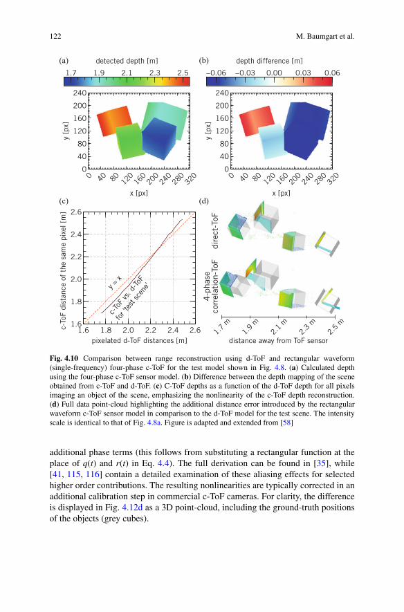
122 M. Baumgart et al.
Fig. 4.10 Comparison between range reconstruction using d-ToF and rectangular waveform(single-frequency) four-phase c-ToF for the test model shown in Fig. 4.8. (a) Calculated depthusing the four-phase c-ToF sensor model. (b) Difference between the depth mapping of the sceneobtained from c-ToF and d-ToF. (c) C-ToF depths as a function of the d-ToF depth for all pixelsimaging an object of the scene, emphasizing the nonlinearity of the c-ToF depth reconstruction.(d) Full data point-cloud highlighting the additional distance error introduced by the rectangularwaveform c-ToF sensor model in comparison to the d-ToF model for the test scene. The intensityscale is identical to that of Fig. 4.8a. Figure is adapted and extended from [58]
additional phase terms (this follows from substituting a rectangular function at theplace of q(t) and r(t) in Eq. 4.4). The full derivation can be found in [35], while[41, 115, 116] contain a detailed examination of these aliasing effects for selectedhigher order contributions. The resulting nonlinearities are typically corrected in anadditional calibration step in commercial c-ToF cameras. For clarity, the differenceis displayed in Fig. 4.12d as a 3D point-cloud, including the ground-truth positionsof the objects (grey cubes).
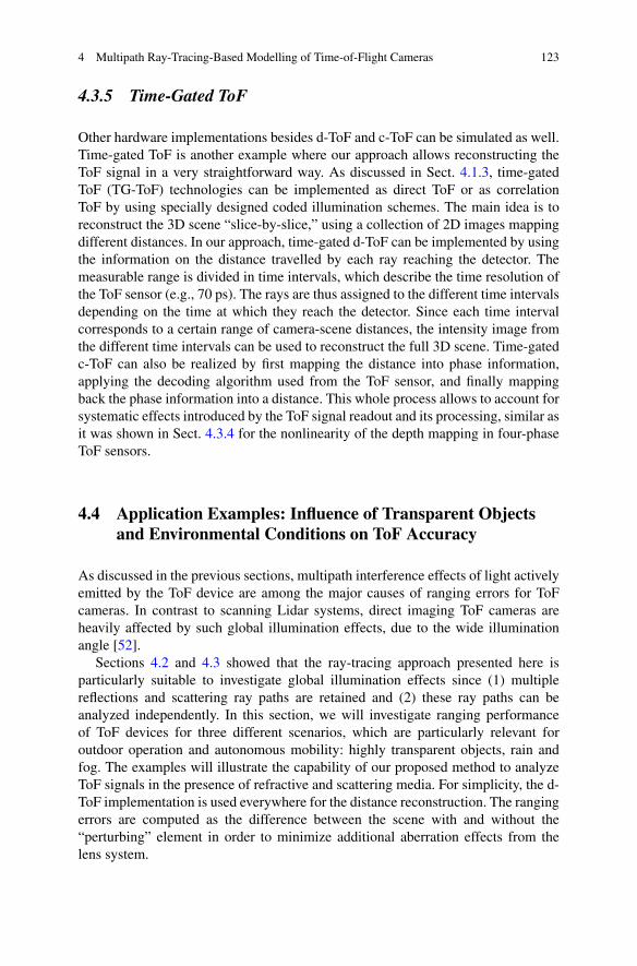
4 Multipath Ray-Tracing-Based Modelling of Time-of-Flight Cameras 123
4.3.5 Time-Gated ToF
Other hardware implementations besides d-ToF and c-ToF can be simulated as well.Time-gated ToF is another example where our approach allows reconstructing theToF signal in a very straightforward way. As discussed in Sect. 4.1.3, time-gatedToF (TG-ToF) technologies can be implemented as direct ToF or as correlationToF by using specially designed coded illumination schemes. The main idea is toreconstruct the 3D scene “slice-by-slice,” using a collection of 2D images mappingdifferent distances. In our approach, time-gated d-ToF can be implemented by usingthe information on the distance travelled by each ray reaching the detector. Themeasurable range is divided in time intervals, which describe the time resolution ofthe ToF sensor (e.g., 70 ps). The rays are thus assigned to the different time intervalsdepending on the time at which they reach the detector. Since each time intervalcorresponds to a certain range of camera-scene distances, the intensity image fromthe different time intervals can be used to reconstruct the full 3D scene. Time-gatedc-ToF can also be realized by first mapping the distance into phase information,applying the decoding algorithm used from the ToF sensor, and finally mappingback the phase information into a distance. This whole process allows to account forsystematic effects introduced by the ToF signal readout and its processing, similar asit was shown in Sect. 4.3.4 for the nonlinearity of the depth mapping in four-phaseToF sensors.
4.4 Application Examples: Influence of Transparent Objectsand Environmental Conditions on ToF Accuracy
As discussed in the previous sections, multipath interference effects of light activelyemitted by the ToF device are among the major causes of ranging errors for ToFcameras. In contrast to scanning Lidar systems, direct imaging ToF cameras areheavily affected by such global illumination effects, due to the wide illuminationangle [52].
Sections 4.2 and 4.3 showed that the ray-tracing approach presented here isparticularly suitable to investigate global illumination effects since (1) multiplereflections and scattering ray paths are retained and (2) these ray paths can beanalyzed independently. In this section, we will investigate ranging performanceof ToF devices for three different scenarios, which are particularly relevant foroutdoor operation and autonomous mobility: highly transparent objects, rain andfog. The examples will illustrate the capability of our proposed method to analyzeToF signals in the presence of refractive and scattering media. For simplicity, the d-ToF implementation is used everywhere for the distance reconstruction. The rangingerrors are computed as the difference between the scene with and without the“perturbing” element in order to minimize additional aberration effects from thelens system.
124 M. Baumgart et al.
4.4.1 Influence of a Glass Window in Front of the Scene
The antireflective coating of the ToF camera lens reduces the influence of lensreflections on the depth calculation to a minimum. In a real-world scenario, however,it is plausible to encounter semi-transparent or highly transparent objects withoutantireflective coating. To examine their influence on the ToF ranging accuracy, thetest scene was modified by adding an (uncoated) glass window in front of part ofthe scene.
The window, modelled as a 1 cm thick N-BK7 quartz glass plate, is positioned1 m away from the ToF camera and covers only the left half of the scene (Fig. 4.11a).Around 4% of the incoming light perpendicular to the glass surface is reflectedas given by the Fresnel equations. Additionally, a 1% Gaussian scattering (withparameters analogous to the surfaces of the cubes, see also Eq. 4.11) was addedto mimic surface roughness and glass impurities. The glass window is orientedperpendicular to the ToF sensor and is positioned in such a way that light directlyreflected from its surface does not hit the receiving optics. In fact, if the directreflection would hit the sensor, the intensity of the directly reflected light wouldcompletely exceed the scattered light from the scene, and the scene behind the glasswould not be detected. The modelled scenario, instead, deals with a more subtlesituation, where the direct signal from the glass window is expected to be very small.
Three main effects are expected to influence the depth estimation. The first iscaused by light backscattered from the window prior to reaching the scene (directbackscattering). These rays image the presence of the window on the sensor, butwhen the window image overlaps with the image of the cubes, they cause anunderestimation of the distances of the cubes. The second effect arises from rayswhich, after reaching the scene, hit the glass window, are either reflected or scatteredback towards the cubes and finally are scattered back to the ToF detector. The lasteffect is caused by rays undergoing multiple reflections within the glass plate. Thelast two effects will both contribute to an overestimation of the scene distance.
Figure 4.11b shows the point-cloud data. Figures 4.11c, d show the intensitydetected by the sensor and the reconstructed distance, respectively. Figure 4.11eshows the ranging difference induced by the presence of the glass window. Thepresence of the window is evident where its image does not overlap with the imageof other cubes, as it can be seen in both the intensity map and in the distance map.The size of the window is overestimated because it is not in the focus of the ToFcamera optics. In the distance map, the window appears as an obstacle located about1.2 m away from the scene, while only the outer borders of the glass are correctlyestimated at a distance of 1 m. The overestimation of the distance of the windowcan be explained by observing that the window is imaged by rays that are directlybackscattered towards the sensor before any interaction with the rest of the scene.Since the window is highly transparent and weakly reflecting, these backscatteredrays overlap with rays undergoing multiple beam reflections between the cubes andthe window, and therefore contribute with a significantly longer optical path. Onlyat the glass edges, where the direct backscattering contribution is dominant and the
4 Multipath Ray-Tracing-Based Modelling of Time-of-Flight Cameras 125
Fig. 4.11 Glass window influence. (a) Test scene from Fig. 4.7 after adding an uncoated N-BK7window in front of part of the scene. (b) 3D point-cloud data. (c) Intensity and (d) calculated depthimages using the global magnification factor correspondence. (e) Depth difference between thedepth retrieved with (panel d) and without (Fig. 4.8b) glass window

126 M. Baumgart et al.
multiple reflection contribution is partially hindered by scattering at the glass edge,the distance of the window is estimated correctly.
Similar to the window, also the distance of the cubes behind the window isoverestimated. The overestimation is due to the balance between the backscatteringfrom the window surface and the multiple reflections events between the 4%-reflective glass window and the scattering surfaces of the cubes. As the latter aredominating, the distance of the cubes is overestimated.
4.4.2 Effect of Environmental Conditions
In Sect. 4.1.2 we observed that lidar devices are extensively used for atmosphericdata collection and analysis [31] as they are sensitive to atmospheric particles andgases. While this enhanced sensitivity is an advantage for mapping rain or aerosoldistributions in the atmosphere, it becomes detrimental for ranging applicationsin rainy or foggy conditions. The light reflected, refracted, or scattered by waterdroplets located between the sensor and the scene causes global illumination effectswhich in turn affect the sensor performance in different ways. Backscattered andbackreflected light will lead to an underestimation of the scene distance and increasethe background noise, while single and multiple scattering or reflection events,prior or after interaction with the scene, will cause an overestimation of the scenedistances. The net result will depend on the relative contribution of each effect.
4.4.2.1 Influence of Rain Droplets Between the ToF Camera and the Scene
Figures 4.13a, c, e show the simulation setup implemented to determine the effectof rain droplets on the range accuracy of ToF cameras. The camera model and thescene are identical to those described in Sect. 4.3.1. The rainfall event is modelledas an ensemble of spherical water droplets of different sizes located between theToF camera and the scene. The droplet distribution N(D) is described by a modifiedGamma function of the form
N(D) = NG Dαe−�D (4.13)
where D is the droplet diameter. The other parameters are determined according tothe model presented in [117]. Accordingly, α = 2.160 and the parameters NG and �
are functions of the liquid water content (LWC) expressed in g/m3 and the rainfallrate R, expressed in mm/h:
LWC = 0.062 R0.913 (4.14)
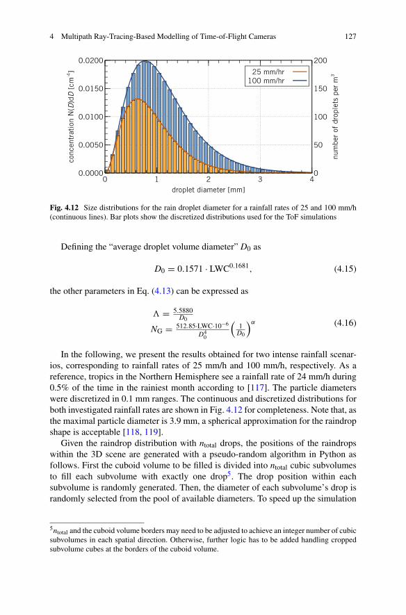
4 Multipath Ray-Tracing-Based Modelling of Time-of-Flight Cameras 127
Fig. 4.12 Size distributions for the rain droplet diameter for a rainfall rates of 25 and 100 mm/h(continuous lines). Bar plots show the discretized distributions used for the ToF simulations
Defining the “average droplet volume diameter” D0 as
D0 = 0.1571 · LWC0.1681, (4.15)
the other parameters in Eq. (4.13) can be expressed as
� = 5.5880D0
NG = 512.85·LWC·10−6
D40
(1
D0
)α (4.16)
In the following, we present the results obtained for two intense rainfall scenar-ios, corresponding to rainfall rates of 25 mm/h and 100 mm/h, respectively. As areference, tropics in the Northern Hemisphere see a rainfall rate of 24 mm/h during0.5% of the time in the rainiest month according to [117]. The particle diameterswere discretized in 0.1 mm ranges. The continuous and discretized distributions forboth investigated rainfall rates are shown in Fig. 4.12 for completeness. Note that, asthe maximal particle diameter is 3.9 mm, a spherical approximation for the raindropshape is acceptable [118, 119].
Given the raindrop distribution with ntotal drops, the positions of the raindropswithin the 3D scene are generated with a pseudo-random algorithm in Python asfollows. First the cuboid volume to be filled is divided into ntotal cubic subvolumesto fill each subvolume with exactly one drop5. The drop position within eachsubvolume is randomly generated. Then, the diameter of each subvolume’s drop israndomly selected from the pool of available diameters. To speed up the simulation
5ntotal and the cuboid volume borders may need to be adjusted to achieve an integer number of cubicsubvolumes in each spatial direction. Otherwise, further logic has to be added handling croppedsubvolume cubes at the borders of the cuboid volume.
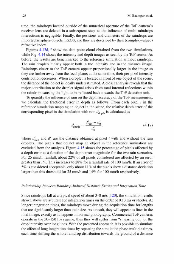
128 M. Baumgart et al.
time, the raindrops located outside of the numerical aperture of the ToF camera’sreceiver lens are deleted in a subsequent step, as the influence of multi-raindropsinteractions is negligible. Finally, the positions and diameters of the raindrops areimported as sphere objects in ZOS, and they are described by their (complex-valued)refractive index.
Figures 4.13d, f show the data point-cloud obtained from the two simulations,while Fig. 4.14 shows the intensity and depth images as seen by the ToF sensor. Asbefore, the results are benchmarked to the reference simulation without raindrops.The rain droplets clearly appear both in the intensity and in the distance image.Raindrops closer to the ToF camera appear proportionally larger in the image asthey are further away from the focal plane; at the same time, their per-pixel intensitycontribution decreases. When a droplet is located in front of one object of the scene,the distance of the object is locally underestimated. A closer analysis reveals that themajor contribution to the droplet signal arises from total internal reflections withinthe raindrop, causing the light to be reflected back towards the ToF detection unit.
To quantify the influence of rain on the depth accuracy of the ToF measurement,we calculate the fractional error in depth as follows: From each pixel i in thereference simulation mapping an object in the scene, the relative depth error of thecorresponding pixel in the simulation with rain εi
depth is calculated as
εidepth = di
rain − di0
di0
, (4.17)
where dirain and di
0 are the distance obtained at pixel i with and without the raindroplets. The pixels that do not map an object in the reference simulation areexcluded from the analysis. Figure 4.15 shows the percentage of pixels affected bya depth error as a function of the depth error magnitude for the two rain scenarios.For 25 mm/h. rainfall, about 22% of all pixels considered are affected by an errorgreater than 1%. This increases to 28% for a rainfall rate of 100 mm/h. If an error of5% is considered acceptable, only about 11% of the pixels show a distance deviationlarger than this threshold for 25 mm/h and 14% for 100 mm/h respectively.
Relationship Between Raindrop-Induced Distance Errors and Integration Time
Since raindrops fall at a typical speed of about 3–8 m/s [120], the simulation resultsshown above are accurate for integration times on the order of 0.13 ms or shorter. Atlonger integration times, the raindrops move during the acquisition time for lengthsthat are significantly larger than their size. As a result, they will appear as lines in thefinal image, exactly as it happens in normal photography. Commercial ToF camerasoperate in the 50–150 fps regime, thus they will suffer from “smearing out” of thedrop intensity over long lines. With the presented approach, it is possible to simulatethe effect of long integration times by repeating the simulation phase multiple times,each time shifting the whole raindrop distribution towards the ground of a distance
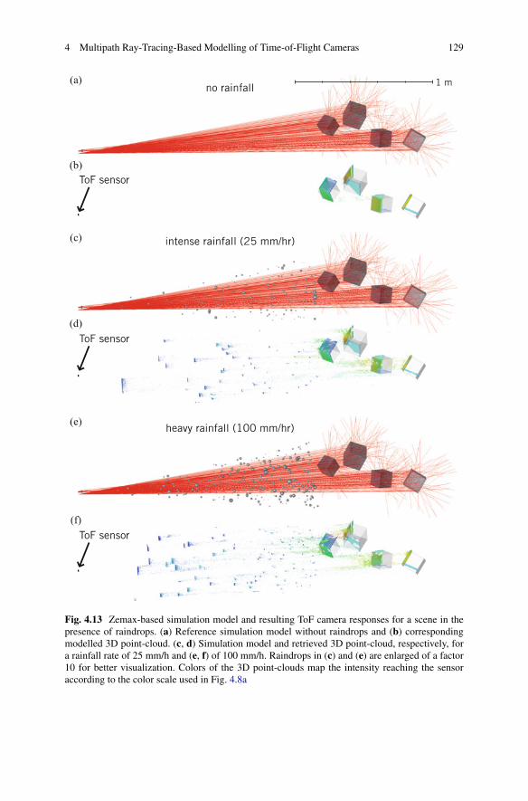
4 Multipath Ray-Tracing-Based Modelling of Time-of-Flight Cameras 129
Fig. 4.13 Zemax-based simulation model and resulting ToF camera responses for a scene in thepresence of raindrops. (a) Reference simulation model without raindrops and (b) correspondingmodelled 3D point-cloud. (c, d) Simulation model and retrieved 3D point-cloud, respectively, fora rainfall rate of 25 mm/h and (e, f) of 100 mm/h. Raindrops in (c) and (e) are enlarged of a factor10 for better visualization. Colors of the 3D point-clouds map the intensity reaching the sensoraccording to the color scale used in Fig. 4.8a
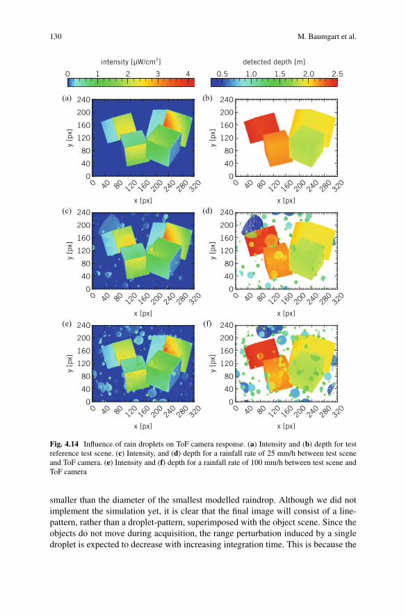
130 M. Baumgart et al.
Fig. 4.14 Influence of rain droplets on ToF camera response. (a) Intensity and (b) depth for testreference test scene. (c) Intensity, and (d) depth for a rainfall rate of 25 mm/h between test sceneand ToF camera. (e) Intensity and (f) depth for a rainfall rate of 100 mm/h between test scene andToF camera
smaller than the diameter of the smallest modelled raindrop. Although we did notimplement the simulation yet, it is clear that the final image will consist of a line-pattern, rather than a droplet-pattern, superimposed with the object scene. Since theobjects do not move during acquisition, the range perturbation induced by a singledroplet is expected to decrease with increasing integration time. This is because the
4 Multipath Ray-Tracing-Based Modelling of Time-of-Flight Cameras 131
Fig. 4.15 Error on the depth accuracy of the ToF sensor caused by rain between the objects and thesensor for rainfall rates of 25 and 100 mm/h. (a) Non-cumulative and (b) cumulative distributionof the depth errors
relative contribution of the intensity reflected back from each rain droplet to thetotal ToF signal decreases due to the relative motion of the droplet with respect tothe object behind it. A competing effect occurs at longer integration times wherereflections from several droplets can be averaged at the sensor and in turn willincrease the range perturbation again. Simultaneously, a larger area of the scenewill be affected by a range error. Therefore, the final effect will strongly dependnot just on the integration time, but also on (1) the details of the scene (e.g., thesurface properties), (2) its distance (more distant scenes scatter back less light,while simultaneously the number of raindrops between camera and scene increases)and (3) the rainfall rate. As a consequence, a precise quantitative estimation of theperformance of a ToF camera in a rainy scenario requires extended and detailedsimulations, accounting for the typical variability in the aforementioned parameters.
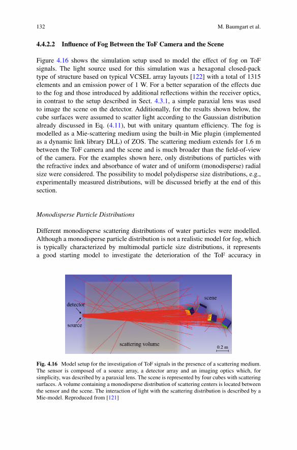
132 M. Baumgart et al.
4.4.2.2 Influence of Fog Between the ToF Camera and the Scene
Figure 4.16 shows the simulation setup used to model the effect of fog on ToFsignals. The light source used for this simulation was a hexagonal closed-packtype of structure based on typical VCSEL array layouts [122] with a total of 1315elements and an emission power of 1 W. For a better separation of the effects dueto the fog and those introduced by additional reflections within the receiver optics,in contrast to the setup described in Sect. 4.3.1, a simple paraxial lens was usedto image the scene on the detector. Additionally, for the results shown below, thecube surfaces were assumed to scatter light according to the Gaussian distributionalready discussed in Eq. (4.11), but with unitary quantum efficiency. The fog ismodelled as a Mie-scattering medium using the built-in Mie plugin (implementedas a dynamic link library DLL) of ZOS. The scattering medium extends for 1.6 mbetween the ToF camera and the scene and is much broader than the field-of-viewof the camera. For the examples shown here, only distributions of particles withthe refractive index and absorbance of water and of uniform (monodisperse) radialsize were considered. The possibility to model polydisperse size distributions, e.g.,experimentally measured distributions, will be discussed briefly at the end of thissection.
Monodisperse Particle Distributions
Different monodisperse scattering distributions of water particles were modelled.Although a monodisperse particle distribution is not a realistic model for fog, whichis typically characterized by multimodal particle size distributions, it representsa good starting model to investigate the deterioration of the ToF accuracy in
Fig. 4.16 Model setup for the investigation of ToF signals in the presence of a scattering medium.The sensor is composed of a source array, a detector array and an imaging optics which, forsimplicity, was described by a paraxial lens. The scene is represented by four cubes with scatteringsurfaces. A volume containing a monodisperse distribution of scattering centers is located betweenthe sensor and the scene. The interaction of light with the scattering distribution is described by aMie-model. Reproduced from [121]
4 Multipath Ray-Tracing-Based Modelling of Time-of-Flight Cameras 133
the presence of scattering centers. In particular, it allows for a straightforwardcorrelation of the ranging errors with the characteristics of the distribution.
For monodisperse distributions of spherical particles with radius a and a particledensity ρ, the single-particle scattering cross-section Csca is defined as
Csca = π a2Qsca (4.18)
where Qsca is the scattering efficiency. The latter is defined as a function of theMie-scattering coefficients an and bn as
Qsca = 2
x2
∞∑
n=1
(2n + 1)(
|an|2 +|bn|2)
(4.19)
where x = ka and k is the wave vector of the light. The total extinction cross-sectionCext of the particle is obtained by summing the scattering and the absorption cross-sections: Cext = Csca + Cabs. A detailed treatment of the Mie-scattering theory andderivation of these expressions can be found in the book of van de Hulst [123].
Given a particle distribution, the extinction coefficient γ determines the attenua-tion according to the Beer-Lambert law
I = I0 e−γL (4.20)
where I and I0 are the transmitted and initial intensities, respectively, and L is thelength of the scattering medium. In general, for a scattering distribution, the totalextinction coefficient γ is composed by a scattering and an absorption contribution.It can be shown that the Mie-scattering extinction coefficient of the distribution γ scais given by
γsca = ρ Csca (4.21)
For practical purposes, several online calculators or software packages offer thepossibility to calculate the Mie-scattering coefficients and/or cross-sections as afunction of the wavelength of the light, the particle size, and its refractive index.For the examples in this chapter, the total absorption cross-section can be considerednegligible as the absorption coefficient of water is extremely small at the wavelengthconsidered, and thus γ ≈ γ sca.
Table 4.2 lists the parameters of the scattering distributions considered in thiswork. Figures 4.17b–e show the simulated point-cloud data for all distributions(1–4), compared to the simulated point-cloud in the absence of scattering (Fig.4.17a). The presence of scattering particles appears as a spatially inhomogeneous,diffuse background noise which is more intense on the detector side closer tothe source. This spatial inhomogeneity is caused by the combined effect of theangular distribution of Mie-scattering and the acceptance angle of the receiveroptics. Besides the background noise, the distance of the scene objects is system-
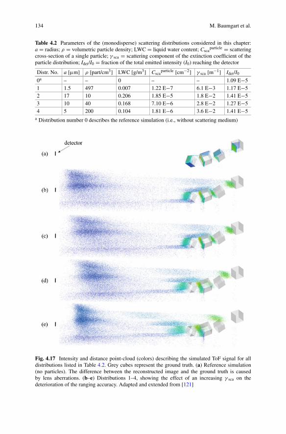
134 M. Baumgart et al.
Table 4.2 Parameters of the (monodisperse) scattering distributions considered in this chapter:a = radius; ρ = volumetric particle density; LWC = liquid water content; Csca
particle = scatteringcross-section of a single particle; γ sca = scattering component of the extinction coefficient of theparticle distribution; Idet/I0 = fraction of the total emitted intensity (I0) reaching the detector
Distr. No. a [μm] ρ [part/cm3] LWC [g/m3] Cscaparticle [cm−2] γ sca [m−1] Idet/I0
0a – – 0 – – 1.09 E−51 1.5 497 0.007 1.22 E−7 6.1 E−3 1.17 E−52 17 10 0.206 1.85 E−5 1.8 E−2 1.41 E−53 10 40 0.168 7.10 E−6 2.8 E−2 1.27 E−54 5 200 0.104 1.81 E−6 3.6 E−2 1.41 E−5
a Distribution number 0 describes the reference simulation (i.e., without scattering medium)
Fig. 4.17 Intensity and distance point-cloud (colors) describing the simulated ToF signal for alldistributions listed in Table 4.2. Grey cubes represent the ground truth. (a) Reference simulation(no particles). The difference between the reconstructed image and the ground truth is causedby lens aberrations. (b–e) Distributions 1–4, showing the effect of an increasing γ sca on thedeterioration of the ranging accuracy. Adapted and extended from [121]
4 Multipath Ray-Tracing-Based Modelling of Time-of-Flight Cameras 135
atically underestimated, while simultaneously the intensity at the detector (Idet) issystematically larger than that measured without the scattering medium. For the sakeof clarity, the fraction of emitted intensity reaching the detector (Idet/I0) is listed inthe last column of Table 4.2.
As discussed in the beginning of Sect. 4.4.2, an underestimation of the objectdistance indicates the presence of a dominant multipath interference contributionfrom light backscattered prior to reaching the scene (direct backscattering). Thishypothesis can be confirmed by analyzing the rays reaching the detector accordingto their intensity and the interactions they experienced on their optical path. Theresults of such an analysis are summarized in the two histograms of Fig. 4.18. In Fig.4.18a, the absolute power reaching the detector is plotted for the different possibleoptical paths and for all scattering distributions. Figure 4.18b shows the relativepower in each optical path. For each entry, the distributions are ordered from left toright with increasing scattering extinction coefficient γ sca. Three major conclusionscan be derived from the histogram. First, as expected the intensity arising from raysthat interact exclusively with the scene decreases monotonically with rising γ sca (seealso inset in Fig. 4.18a). Second, the largest contribution arising from the particledistribution is indeed due to direct backscattering, which explains both the dominantunderestimation of the object distance and the slight increase of intensity at thedetector in the presence of scattering particles. Third, multiple scattering events arerare, and typically contribute <0.1% to the total signal.
Presenting a deep analysis of ranging errors induced by global illumination fromextended scattering media and strategies for their correction are topics that go wellbeyond the scope of this chapter. However, having demonstrated how to generateand analyze point-cloud data for a scene in the presence of a scattering medium, anatural question is whether and how this information can be used to devise strategiesto minimize the observed ranging errors. A simple example to illustrate a possiblestrategy is shown in Fig. 4.19. As can be seen, filtering out all signals from shortdistances effectively improves the ranging accuracy.
Figure 4.19a shows the mapped scene in the absence of scattering particles(reference scene), while Fig. 4.19b shows the reconstructed distance for the particledistribution number 3 assuming a 12-bit ADC (see Fig. 4.17d and Table 4.2 forthe details). Figures 4.19c, d show the reconstructed depth maps obtained whenneglecting all rays sampling a sensor-scene distance shorter than 61 cm and 84 cm,respectively. These values correspond to about one quarter and one third of thetotal scene distance and remove 36% and 52% of the fog thickness, respectively.Distant surfaces and surfaces forming the largest angles with the ToF camera aremost affected by ranging errors since they scatter less intensity to the detector(see also Fig. 4.8a). Filtering out the signal from fog layers close to the sensorremoves backscattered intensity overlapping with the signal coming from the scene.Therefore, the relative improvement due to this type of filtering is expected to belarge for distant and tilted surfaces, while the effect on surfaces that backscatter alarge amount of light to the detector is expected to be small. The reduction of thedistance error by such a filtering strategy is quantified in Fig. 4.20 for the five areasmarked in Fig. 4.19a, and confirms the expected trend. The most significant effect is
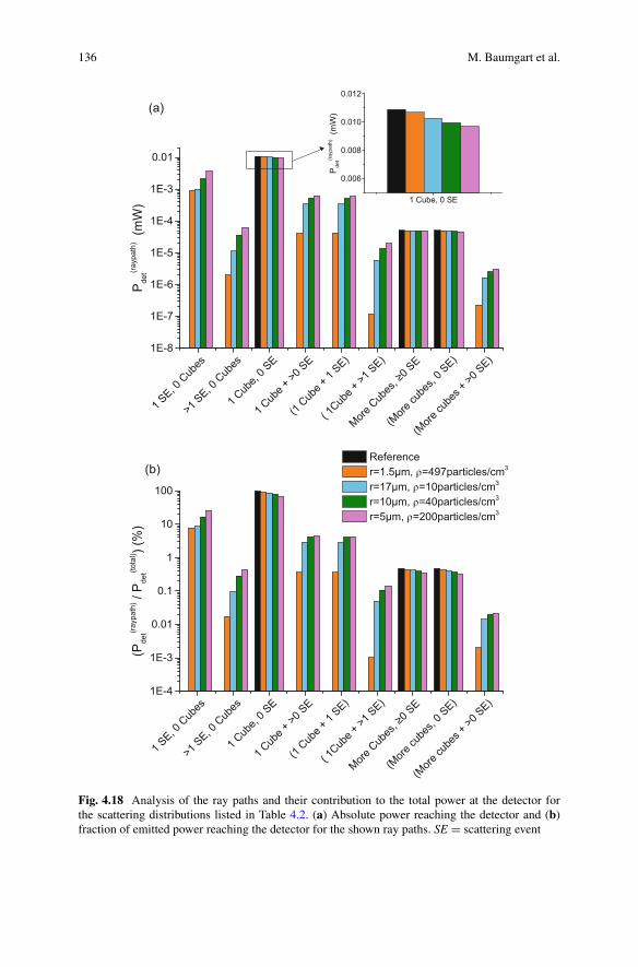
136 M. Baumgart et al.
Fig. 4.18 Analysis of the ray paths and their contribution to the total power at the detector forthe scattering distributions listed in Table 4.2. (a) Absolute power reaching the detector and (b)fraction of emitted power reaching the detector for the shown ray paths. SE = scattering event
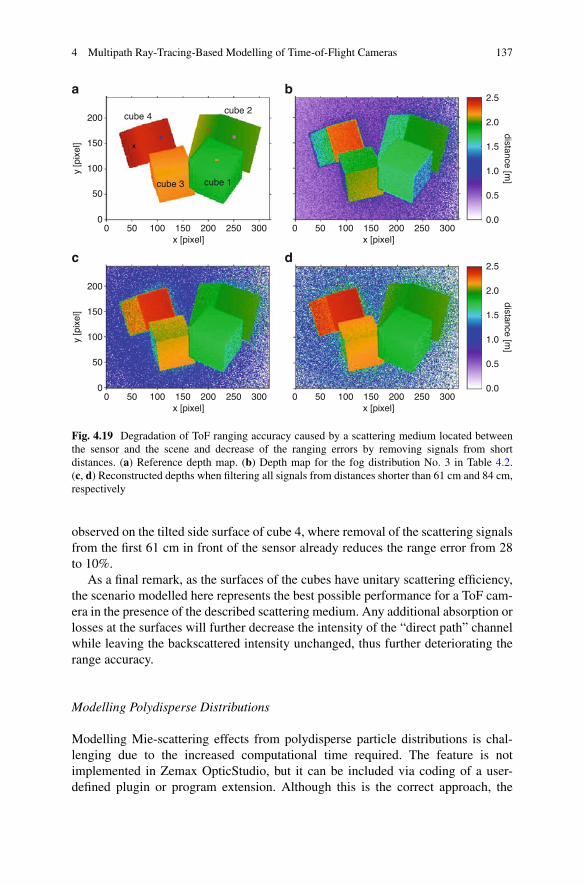
4 Multipath Ray-Tracing-Based Modelling of Time-of-Flight Cameras 137
200
150
cube 4cube 2
2.5
2.0
distance [m]
1.5
1.0
0.5
0.0
cube 3 cube 1
y [p
ixel
]
x [pixel]
a
100
50
00 50 100 200 300150 250
x [pixel]
b
0 50 100 200 300150 250
200
150
2.5
2.0
distance [m]
1.5
1.0
0.5
0.0
y [p
ixel
]
x [pixel]
c
100
50
00 50 100 200 300150 250
x [pixel]
d
0 50 100 200 300150 250
Fig. 4.19 Degradation of ToF ranging accuracy caused by a scattering medium located betweenthe sensor and the scene and decrease of the ranging errors by removing signals from shortdistances. (a) Reference depth map. (b) Depth map for the fog distribution No. 3 in Table 4.2.(c, d) Reconstructed depths when filtering all signals from distances shorter than 61 cm and 84 cm,respectively
observed on the tilted side surface of cube 4, where removal of the scattering signalsfrom the first 61 cm in front of the sensor already reduces the range error from 28to 10%.
As a final remark, as the surfaces of the cubes have unitary scattering efficiency,the scenario modelled here represents the best possible performance for a ToF cam-era in the presence of the described scattering medium. Any additional absorption orlosses at the surfaces will further decrease the intensity of the “direct path” channelwhile leaving the backscattered intensity unchanged, thus further deteriorating therange accuracy.
Modelling Polydisperse Distributions
Modelling Mie-scattering effects from polydisperse particle distributions is chal-lenging due to the increased computational time required. The feature is notimplemented in Zemax OpticStudio, but it can be included via coding of a user-defined plugin or program extension. Although this is the correct approach, the
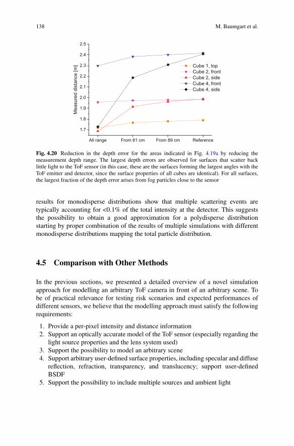
138 M. Baumgart et al.
All range From 61 cm From 89 cm Reference
1.7
1.8
1.9
2.0
2.1
2.2
2.3
2.4
2.5
Mea
sure
d di
stan
ce [m
] Cube 1, topCube 2, frontCube 2, sideCube 4, frontCube 4, side
Fig. 4.20 Reduction in the depth error for the areas indicated in Fig. 4.19a by reducing themeasurement depth range. The largest depth errors are observed for surfaces that scatter backlittle light to the ToF sensor (in this case, these are the surfaces forming the largest angles with theToF emitter and detector, since the surface properties of all cubes are identical). For all surfaces,the largest fraction of the depth error arises from fog particles close to the sensor
results for monodisperse distributions show that multiple scattering events aretypically accounting for <0.1% of the total intensity at the detector. This suggeststhe possibility to obtain a good approximation for a polydisperse distributionstarting by proper combination of the results of multiple simulations with differentmonodisperse distributions mapping the total particle distribution.
4.5 Comparison with Other Methods
In the previous sections, we presented a detailed overview of a novel simulationapproach for modelling an arbitrary ToF camera in front of an arbitrary scene. Tobe of practical relevance for testing risk scenarios and expected performances ofdifferent sensors, we believe that the modelling approach must satisfy the followingrequirements:
1. Provide a per-pixel intensity and distance information2. Support an optically accurate model of the ToF sensor (especially regarding the
light source properties and the lens system used)3. Support the possibility to model an arbitrary scene4. Support arbitrary user-defined surface properties, including specular and diffuse
reflection, refraction, transparency, and translucency; support user-definedBSDF
5. Support the possibility to include multiple sources and ambient light
4 Multipath Ray-Tracing-Based Modelling of Time-of-Flight Cameras 139
6. Account for global illumination (multiple scattering or reflections) and possiblyallow the user to identify the origin and characteristics of the ranging errorscaused by multipath interference (multipath analysis)
7. Support models for different environmental conditions (rain, fog, haze, snow)8. Allow comparison of different hardware schemes9. Provide simulation results “reasonably” fast
10. Be able to account for motion blur11. Ideally, provide a good GUI.
Our approach undoubtedly fulfils points 1–7. A major advantage of the approachis that, for a given scene, a direct comparison between different hardware imple-mentations can be performed completely separated from the ray-tracing by usingone single ray-traced dataset. The major drawback of the approach is the relativelyslow simulation speed due to the ray-tracing software used.
Depending on the complexity of the scene and the interactions within it, thesimulation time can exceed a day (this is especially true for scattering modelsincluding the full physical description of Mie-scattering). As a consequence, motionblur effects can only be evaluated for simple scenes in a reasonable amount of time.In this regard, the CamSim toolbox which was released in the middle of 2018 issuperior to our simulation approach. Using OpenGL and the full power of the GPUto trace the rays results in very short simulation times. However, it needs to beclarified if and how this platform can be extended to properly describe complexmedia, such as refractive objects (like raindrops) or scattering distributions (fog).Table 4.3 shows a comparison between the possibilities presented by our approachand the features of the most common (freeware or publically available) modellingenvironments for ToF cameras.
4.6 Conclusions
In this chapter, we have presented a novel approach to modelling ToF cameras. Ourapproach has several advantages with respect to current simulation environments:
• It allows retaining all optical effects (at least within the geometric optics model),including refraction and multiple reflections and/or scattering. As demonstratedin the examples of the glass window (Sect. 4.4.1) and of the rain droplets(Sect. 4.4.2), this is necessary for a correct modelling of a situation wheremultiple reflections/refraction events take place in the scene and give a significantcontribution to the total intensity reaching the detector. Additionally, such anapproach allows including a physical description of Mie-scattering from densemedia.
• The approach has great versatility due to the possibility to easily modify andcompare different source profiles and detector optics or to test for various scenesurface properties.
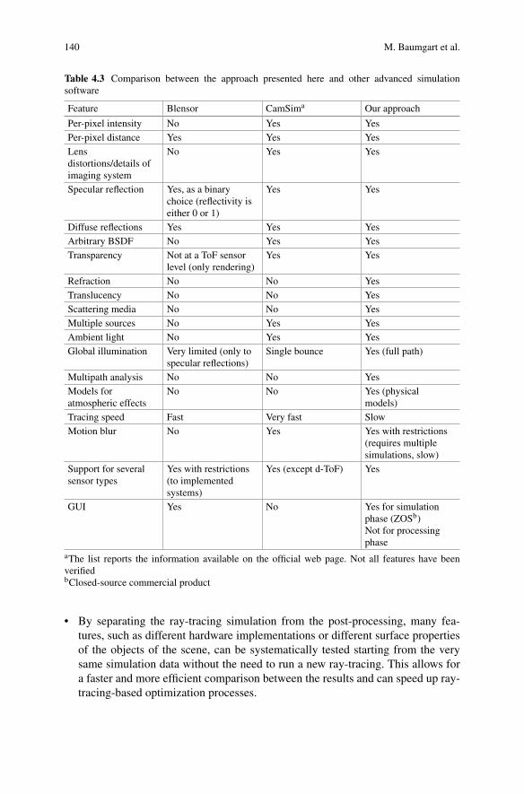
140 M. Baumgart et al.
Table 4.3 Comparison between the approach presented here and other advanced simulationsoftware
Feature Blensor CamSima Our approach
Per-pixel intensity No Yes YesPer-pixel distance Yes Yes YesLensdistortions/details ofimaging system
No Yes Yes
Specular reflection Yes, as a binarychoice (reflectivity iseither 0 or 1)
Yes Yes
Diffuse reflections Yes Yes YesArbitrary BSDF No Yes YesTransparency Not at a ToF sensor
level (only rendering)Yes Yes
Refraction No No YesTranslucency No No YesScattering media No No YesMultiple sources No Yes YesAmbient light No Yes YesGlobal illumination Very limited (only to
specular reflections)Single bounce Yes (full path)
Multipath analysis No No YesModels foratmospheric effects
No No Yes (physicalmodels)
Tracing speed Fast Very fast SlowMotion blur No Yes Yes with restrictions
(requires multiplesimulations, slow)
Support for severalsensor types
Yes with restrictions(to implementedsystems)
Yes (except d-ToF) Yes
GUI Yes No Yes for simulationphase (ZOSb)Not for processingphase
aThe list reports the information available on the official web page. Not all features have beenverifiedbClosed-source commercial product
• By separating the ray-tracing simulation from the post-processing, many fea-tures, such as different hardware implementations or different surface propertiesof the objects of the scene, can be systematically tested starting from the verysame simulation data without the need to run a new ray-tracing. This allows fora faster and more efficient comparison between the results and can speed up ray-tracing-based optimization processes.
4 Multipath Ray-Tracing-Based Modelling of Time-of-Flight Cameras 141
• The possibility to separate contributions arising from different optical paths is apowerful feature that can be used to track the origin of specific effects and devisestrategies to specifically address them.
An important remark is that the implementation proposed here is not (and neverwill be) a real-time simulation environment. It is an approach that is meant to solvethe basic objective we posed at the beginning of this chapter, that is, to help uslearn about the critical phenomena we need to control (or correct for) if we wantto bring ToF technology to the point of being compatible with a safe autonomousoperation in any outdoor scenario we can imagine. As we have shown, our approachcan be used not only to quantify the magnitude of a range error but also to identify itsorigin and to determine how it manifests itself in the resulting ToF image. Achievinga full mapping, quantification, and correction for such ranging errors undoubtedlyrequires much more work. However, many ideas and technologies are already outthere. We believe that the deeper knowledge on the origin of ToF range errorscan give us the key to identify the most suitable technologies to achieve the bestperformances in each and all possible scenarios (be it time-gating, measuring atmultiple frequency, implementing post-processing correction algorithms, a mixtureof these or even new ideas).
Acknowledgments This project has received funding from the Electronic Component Systems forEuropean Leadership Joint Undertaking under grant agreement No 692480. This Joint Undertakingreceives support from the European Union’s Horizon 2020 research and innovation programmeand Germany, Saxony, Spain, Austria, Belgium, and Slovakia. The project IoSense is co-funded byAustrian Research Promotion Agency (FFG). The authors also thank Dr. Jan Steinbrener and Dr.Gerald Auböck for helpful discussions.
References
1. J.J. Koenderink, A.J. van Doorn, A.M.L. Kappers, Depth relief. Perception 24, 115–126(1995)
2. P. Servos, Distance estimation in the visual and visuomotor systems. Exp. Brain Res. 130,35–47 (2000)
3. D. Vishwanath, P.B. Hibbard, Seeing in 3-D with just one eye: Stereopsis without binocularvision. Psychol. Sci. 24, 1673–1685 (2013)
4. A.P. Pentland, A new sense for depth of field. IEEE Trans. Pattern Anal. Mach. Intell. PAMI-9, 523–531 (1987)
5. S. Weiss, D. Scaramuzza, R. Siegwart, Monocular-SLAM–based navigation for autonomousmicro helicopters in GPS-denied environments. J. Field Robot. 28, 854–874 (2011)
6. D. Antensteiner, S. Štolc, T. Pock, A review of depth and normal fusion algorithms. Sensors18, 431 (2018)
7. F. Santoso, M.A. Garratt, M.R. Pickering, M. Asikuzzaman, 3D mapping for visualization ofrigid structures: A review and comparative study. IEEE Sensors J. 16, 1484–1507 (2016)
8. M.T. McCann, K.H. Jin, M. Unser, Convolutional neural networks for inverse problems inimaging: A review. IEEE Signal Process. Mag. 34, 85–95 (2017)
9. B. Girod, G. Greiner, H. Niemann (eds.), Principles of 3D Image Analysis and Synthesis(Springer US, New York, 2002)
142 M. Baumgart et al.
10. N. Lazaros, G.C. Sirakoulis, A. Gasteratos, Review of stereo vision algorithms: Fromsoftware to hardware. Int. J. Optomechatron. 2, 435–462 (2008)
11. S. Zhang, Handbook of 3D Machine Vision: Optical Metrology and Imaging (CRC, BocaRaton, FL, 2013). https://doi.org/10.1201/b13856
12. P.J. Besl, Active optical range imaging sensors, in Advances in Machine Vision, ed. by J. L.C. Sanz, (Springer, New York, 1989), pp. 1–63
13. C. Dal Mutto, P. Zanuttigh, G.M. Cortelazzo, Time-Of-Flight Cameras and MicrosoftKinect™ (Springer-Verlag, New York, 2012)
14. D. Malacara, Optical Metrology of Diffuse Surfaces (Wiley, New York, 2007)15. W.E.K. Middleton, A.F. Spilhaus, Meteorological Instruments, 3rd edn. (University of
Toronto Press, Toronto, ON, 1953)16. A. Javan, Theory of a three-level maser. Phys. Rev. 107, 1579–1589 (1957)17. A.L. Schawlow, C.H. Townes, Infrared and optical masers. Phys. Rev. 112, 1940–1949 (1958)18. T.H. Maiman, Stimulated optical radiation in ruby. Nature 187, 493–494 (1960)19. N.G. Basov, O.N. Krokhin, Y.M. Popov, Generation, amplification, and detection of infrared
and optical radiation by quantum-mechanical systems. Sov. Phys. Usp. 3, 702 (1961)20. M. I. Skolnik (ed.), Radar Handbook, 3. [rev.] edn. (McGraw Hill, New York, NY, 2008)21. M. Jaboyedoff, T. Oppikofer, A. Abellán, M.-H. Derron, A. Loye, R. Metzger, A. Pedrazzini,
Use of LIDAR in landslide investigations: A review. Nat. Hazards 61, 5–28 (2012)22. D.P. Thoma, S.C. Gupta, M.E. Bauer, C.E. Kirchoff, Airborne laser scanning for riverbank
erosion assessment. Remote Sens. Environ. 95, 493–501 (2005)23. J.S. Deems, T.H. Painter, D.C. Finnegan, Lidar measurement of snow depth: A review. J.
Glaciol. 59, 467–479 (2013)24. W.Y. Yan, A. Shaker, N. El-Ashmawy, Urban land cover classification using airborne LiDAR
data: A review. Remote Sens. Environ. 158, 295–310 (2015)25. C. Weitkamp (ed.), Lidar: Range-Resolved Optical Remote Sensing of the Atmosphere
(Springer-Verlag, New York, 2005)26. K. Sassen, The polarization lidar technique for cloud research: A review and current
assessment. Bull. Am. Meteor. Soc. 72, 1848–1866 (1991)27. K. Fredriksson, B. Galle, K. Nyström, S. Svanberg, Lidar system applied in atmospheric
pollution monitoring. Appl. Opt. 18, 2998–3003 (1979)28. A. Papayannis, G. Ancellet, J. Pelon, G. Mégie, Multiwavelength lidar for ozone measure-
ments in the troposphere and the lower stratosphere. Appl. Opt. 29, 467–476 (1990)29. S.W. Henderson, P. Gatt, D. Rees, R.M. Huffaker, P. Gatt, D. Rees, R.M. Huffaker,
Wind Lidar, in Laser Remote Sensing, (Taylor & Francis, Boca Raton, FL, 2005).https://doi.org/10.1201/9781420030754-10
30. A. Sathe, J. Mann, A review of turbulence measurements using ground-based wind lidars.Atmos. Meas. Tech. 6, 3147–3167 (2013)
31. T. Fujii, T. Fukuchi, Laser Remote Sensing (CRC, Boca Raton, FL, 2005)32. M.H. Conde, Compressive Sensing for the Photonic Mixer Device: Fundamentals, Methods
and Results (Springer, Berlin, 2017)33. Rudolf Schwarte. Method and Apparatus for Determining the Phase and/or Amplitude
Information of an Electromagnetic Wave for Photomixing. (1998)34. R. Schwarte, H. Heinol, B. Buxbaum, T. Ringbeck, Z. Xu, K. Hartmann, Principles of three-
dimensional imaging techniques, in Handbook of Computer Vision and Applications: Sensorsand Imaging, (Academic, New York, 1999), pp. 463–484
35. H.P. Stahl, Review of phase-measuring interferometry, in Optical Testing and MetrologyIII: Recent Advances in Industrial Optical Inspection, (International Society for Optics andPhotonics, Bellingham, WA, 1991), pp. 704–720
36. O. Lottner, Investigations of Optical 2D/3D-Imaging with Different Sensors and IlluminationConfigurations (Shaker, Aachen, 2012)
37. T. Ringbeck, T. Möller, B. Hagebeuker, Multidimensional measurement by using 3-D PMDsensors, in Advances in Radio Science, (Copernicus GmbH, Göttingen, 2007), pp. 135–146

4 Multipath Ray-Tracing-Based Modelling of Time-of-Flight Cameras 143
38. L. Pancheri, D. Stoppa, Sensors based on in-pixel photo-mixing devices, in TOF Range-Imaging Cameras, ed. by F. Remondino, D. Stoppa, (Springer, Berlin, 2013), pp. 69–89
39. B.L. Stann, W.C. Ruff, Z.G. Sztankay, Intensity-modulated diode laser radar using frequency-modulation/continuous-wave ranging techniques. Opt. Eng. 35, 3270–3279 (1996)
40. R. Matthey, V. Mitev, Pseudo-random noise-continuous-wave laser radar for surface and cloudmeasurements. Opt. Lasers Eng. 43, 557–571 (2005)
41. J.P. Godbaz, M.J. Cree, A.A. Dorrington, Understanding and ameliorating non-linear phaseand amplitude responses in AMCW lidar. Remote Sens. 4, 21–42 (2012)
42. D. Piatti, F. Remondino, D. Stoppa, State-of-the-art of TOF range-imaging sensors, in TOFRange-Imaging Cameras, ed. by F. Remondino, D. Stoppa, (Springer, Berlin, 2013), pp. 1–9
43. D.M. Burns, V.M. Bright, S.C. Gustafson, E.A. Watson, Optical beam steering using surfacemicromachined gratings and optical phased arrays, in Optical Scanning Systems: Design andApplications, (International Society for Optics and Photonics, Bellingham, WA, 1997), pp.99–111
44. J.K. Doylend, M.J.R. Heck, J.T. Bovington, J.D. Peters, L.A. Coldren, J.E. Bowers, Two-dimensional free-space beam steering with an optical phased array on silicon-on-insulator.Opt Exp. 19, 21595–21604 (2011)
45. A. Yaacobi, J. Sun, M. Moresco, G. Leake, D. Coolbaugh, M.R. Watts, Integrated phasedarray for wide-angle beam steering. Opt. Lett. 39, 4575–4578 (2014)
46. C.V. Poulton, A. Yaacobi, D.B. Cole, M.J. Byrd, M. Raval, D. Vermeulen, M.R. Watts,Coherent solid-state LIDAR with silicon photonic optical phased arrays. Opt. Lett. 42, 4091–4094 (2017)
47. R.A. Jarvis, A perspective on range finding techniques for computer vision. IEEE Trans.Pattern Anal. Mach. Intell. PAMI-5, 122–139 (1983)
48. J.S. Massa, G.S. Buller, A.C. Walker, S. Cova, M. Umasuthan, A.M. Wallace, Time-of-flightoptical ranging system based on time-correlated single-photon counting. Appl. Opt. 37, 7298–7304 (1998)
49. E. Charbon, M. Fishburn, R. Walker, R.K. Henderson, C. Niclass, SPAD-based sensors, inTOF Range-Imaging Cameras, ed. by F. Remondino, D. Stoppa, (Springer, Berlin, 2013), pp.11–38
50. S. Bellisai, D. Bronzi, F.A. Villa, S. Tisa, A. Tosi, F. Zappa, Single-photon pulsed-lightindirect time-of-flight 3D ranging. Opt. Exp. 21, 5086–5098 (2013)
51. N.A.W. Dutton, I. Gyongy, L. Parmesan, R.K. Henderson, Single photon counting perfor-mance and noise analysis of CMOS SPAD-based image sensors. Sensors 16, 1122 (2016)
52. J.P. Godbaz, A.A. Dorrington, M.J. Cree, Understanding and ameliorating mixed pixelsand multipath interference in AMCW lidar, in TOF Range-Imaging Cameras, ed. by F.Remondino, D. Stoppa, (Springer, Berlin, 2013), pp. 91–116
53. M. Hebert, E. Krotkov, 3D measurements from imaging laser radars: How good are they?Image Vis. Comput. 10, 170–178 (1992)
54. M.D. Adams, P.J. Probert, The interpretation of phase and intensity data from AMCW lightdetection sensors for reliable ranging. Int. J. Robot. Res. 15, 441–458 (1996)
55. M. Schmidt, Analysis, Modeling and Dynamic Optimization of 3D Time-Of-Flight ImagingSystems (Ruperto-Carola University of Heidelberg, Heidelberg, 2011)
56. M. Grzegorzek, C. Theobalt, R. Koch, A. Kolb (eds.), Time-of-Flight and Depth Imaging.Sensors, Algorithms and Applications: Dagstuhl Seminar 2012 and GCPR Workshop onImaging New Modalities (Springer, Berlin, 2013)
57. S.N.R. Meister, On Creating Reference Data for Performance Analysis inImage Processing (University of Heidelberg, Heidelberg, Germany, 2014).https://doi.org/10.11588/heidok.00016193
58. M. Baumgart, N. Druml, M. Consani, Procedure enabling simulation and in-depth analysisof optical effects in camera-based time-of-flight sensors, in ISPRS - International Archives ofthe Photogrammetry, Remote Sensing and Spatial Information Sciences, (Copernicus GmbH,Göttingen, 2018), pp. 83–89

144 M. Baumgart et al.
59. R. Horaud, Hansard M, G. Evangelidis, C. Ménier, An overview of depth cameras and rangescanners based on time-of-flight technologies. Mach. Vis. Appl. 27, 1005–1020 (2016)
60. S.T.S. Holmström, U. Baran, H. Urey, MEMS laser scanners: A review. J. Microelectromech.Syst. 23, 259–275 (2014)
61. H.W. Yoo, N. Druml, D. Brunner, C. Schwarzl, T. Thurner, M. Hennecke, G. Schitter, MEMS-based lidar for autonomous driving. Elektrotech. Infotech. 135, 408–415 (2018)
62. S. Fuchs, Multipath interference compensation in time-of-flight camera images, in 2010 20thInternational Conference on Pattern Recognition, (2010), pp. 3583–3586
63. A.A. Dorrington, J.P. Godbaz, M.J. Cree, A.D. Payne, L.V. Streeter, Separating true rangemeasurements from multi-path and scattering interference in commercial range cameras, inThree-Dimensional Imaging, Interaction, and Measurement, (International Society for Opticsand Photonics, Bellingham, WA, 2011), p. 786404
64. J.P. Godbaz, M.J. Cree, A.A. Dorrington, Closed-form inverses for the mixed pixel/multipathinterference problem in AMCW lidar. Comput. Imag. X. 8296, 829618 (2012).https://doi.org/10.1117/12.909778
65. A. Kadambi, R. Whyte, A. Bhandari, L. Streeter, C. Barsi, A. Dorrington, R. Raskar, Codedtime of flight cameras: Sparse deconvolution to address multipath interference and recovertime profiles. ACM Trans. Graph. 32, 167:1–167:10 (2013)
66. A. Kirmani, A. Benedetti, P.A. Chou, SPUMIC: Simultaneous phase unwrapping andmultipath interference cancellation in time-of-flight cameras using spectral methods,in 2013 IEEE International Conference on Multimedia and Expo (ICME), (2013).https://doi.org/10.1109/ICME.2013.6607553
67. F. Heide, M.B. Hullin, J. Gregson, W. Heidrich, Low-budget transient imaging using photonicmixer devices. ACM Trans. Graph. 32, 45 (2013)
68. D. Freedman, Y. Smolin, E. Krupka, I. Leichter, M. Schmidt, SRA: fast removal of generalmultipath for ToF sensors, Computer Vision—ECCV 2014 (2014), pp. 234–249. isbn:978-3-319-10590-1
69. D. Jiménez, D. Pizarro, M. Mazo, S. Palazuelos, Modelling and correction of multipathinterference in time of flight cameras, in 2012 IEEE Conference on Computer Vision andPattern Recognition, (2012), pp. 893–900. https://doi.org/10.1109/CVPR.2012.6247763
70. M. O’Toole, F. Heide, L. Xiao, M.B. Hullin, W. Heidrich, K.N. Kutulakos, Temporalfrequency probing for 5D transient analysis of global light transport. ACM Trans. Graph.33, 87:1–87:11 (2014)
71. J. Lin, Y. Liu, M.B. Hullin, Q. Dai, Fourier analysis on transient imaging with a multi-frequency time-of-flight camera. 2014 IEEE Conference on Computer Vision and PatternRecognition (2014), pp. 3230–3237. https://doi.org/10.1109/CVPR.2014.419
72. M. Gupta, S.K. Nayar, M.B. Hullin, J. Martin, Phasor imaging: A generalization ofcorrelation-based time-of-flight imaging. ACM Trans Graph 34, 156:1–156:18 (2015)
73. N. Naik, A. Kadambi, C. Rhemann, S. Izadi, R. Raskar, S.B. Kang, A light transport modelfor mitigating multipath interference in time-of-flight sensors, in 2015 IEEE Conference onComputer Vision and Pattern Recognition (CVPR), (2015), pp. 73–81
74. C. Peters, J. Klein, M.B. Hullin, R. Klein, Solving Trigonometric Moment Prob-lems for Fast Transient Imaging. ACM Trans. Graph. 6(34) (2015). 220:1–220:11. doi:10.1145/2816795.2818103
75. H. Qiao, J. Lin, Y. Liu, M.B. Hullin, Q. Dai, Resolving transient time profile inToF imaging via log-sum sparse regularization. Opt. Lett. 6(40), 918–921 (2015).https://doi.org/10.1364/OL.40.000918
76. A. Kadambi, V. Taamazyan, S. Jayasuriya, R. Raskar. Frequency domain TOF: encodingobject depth in modulation frequency. arXiv:1503.01804 [cs] (2015)
77. R. Whyte, L. Streeter, M.J. Cree, A.A. Dorrington, Resolving multiple propagation paths intime of flight range cameras using direct and global separation methods. Opt. Eng. 11(54),1560–2303 (2015). https://doi.org/10.1117/1.OE.54.11.113109
78. A. Jarabo, B. Masia, J. Marco, D. Gutierrez, Recent advances in transient imaging: Acomputer graphics and vision perspective. Vis. Inform. 1, 65–79 (2017)

4 Multipath Ray-Tracing-Based Modelling of Time-of-Flight Cameras 145
79. J. Busck, H. Heiselberg, Gated viewing and high-accuracy three-dimensional laser radar.Appl. Opt. 43, 4705–4710 (2004)
80. A. Kirmani, T. Hutchison, J. Davis, R. Raskar, Looking around the corner using transientimaging, in 2009 IEEE 12th International Conference on Computer Vision, (2009), pp. 159–166
81. A. Velten, T. Willwacher, O. Gupta, A. Veeraraghavan, M.G. Bawendi, R. Raskar, Recov-ering three-dimensional shape around a corner using ultrafast time-of-flight imaging. Nat.Commun. 3, 745 (2012)
82. M. Laurenzis, A. Velten, Nonline-of-sight laser gated viewing of scattered photons. Opt. Eng.53, 023102 (2014)
83. R. Pandharkar, A. Velten, A. Bardagjy, E. Lawson, M. Bawendi, R. Raskar, Estimating motionand size of moving non-line-of-sight objects in cluttered environments. CVPR 2011, 265–272(2011)
84. A. Velten, D. Wu, A. Jarabo, B. Masia, C. Barsi, C. Joshi, E. Lawson, M. Bawendi, D.Gutierrez, R. Raskar, Femto-photography: capturing and visualizing the propagation of light.ACM Trans. Graph. 32, 44 (2013)
85. B. Heshmat, G. Satat, C. Barsi, R. Raskar, Single-shot ultrafast imaging using parallax-free alignment with a tilted lenslet array, in 2014 conference on lasers and electro-optics(CLEO)—laser science to photonic applications, (2014), pp. 1–2
86. G. Gariepy, N. Krstajic, R. Henderson, C. Li, R.R. Thomson, G.S. Buller, B. Heshmat, R.Raskar, J. Leach, D. Faccio, Single-photon sensitive light-in-fight imaging. Nat. Commun. 6,6021 (2015)
87. Laser Imaging Through Obscurants|LITO Technologies. https://litotechnologies.com/.Accessed 30 Jan 2019
88. Panasonic Develops Long-range TOF Image Sensor|Headquarters News. In Panasonic News-room Global. http://news.panasonic.com/global/press/data/2018/06/en180619-3/en180619-3.html. Accessed 30 Jan 2019
89. Y. Hirose, S. Koyama, M. Ishii, et al., A 250 m direct time-of-flight ranging system basedon a synthesis of sub-ranging images and a vertical avalanche photo-diodes (VAPD) CMOSimage sensor. Sensors 18, 3642 (2018)
90. T. Kavli, T. Kirkhus, J.T. Thielemann, B. Jagielski, Modelling and compensating measure-ment errors caused by scattering in time-of-flight cameras, in Two- and Three-DimensionalMethods for Inspection and Metrology VI, (International Society for Optics and Photonics,Bellingham, WA, 2008), p. 706604
91. S. Jamtsho, D.D. Lichti, Modelling Scattering Distortion in 3 D Range Camera, in Proceed-ings of the International Archives of Photogrammetry, (2010), pp. 299–304
92. J. Marco, Q. Hernandez, A. Muñoz, Y. Dong, A. Jarabo, M.H. Kim, X. Tong, D. Gutierrez,DeepToF: Off-the-shelf real-time correction of multipath interference in time-of-flight imag-ing. ACM Trans. Graph. 36, 219:1–219:12 (2017)
93. A. Bhandari, A. Kadambi, R. Whyte, C. Barsi, M. Feigin, A. Dorrington, R. Raskar, Resolvingmultipath interference in time-of-flight imaging via modulation frequency diversity and sparseregularization. Opt. Lett. 39, 1705–1708 (2014)
94. F. Heide, L. Xiao, A. Kolb, M.B. Hullin, W. Heidrich, Imaging in scattering media usingcorrelation image sensors and sparse convolutional coding. Opt. Exp. 22, 26338–26350(2014)
95. S. Achar, J.R. Bartels, W.L. Whittaker, K.N. Kutulakos, S.G. Narasimhan, Epipolar time-of-flight imaging. ACM Trans. Graph. 36, 37:1–37:8 (2017)
96. M. Pharr, W. Jakob, G. Humphreys, Physically Based Rendering: From Theory to Implemen-tation, 3rd edn. (Elsevier, Morgan Kaufmann, Amsterdam, 2017)
97. P. Shirley, R.K. Morley, P.-P. Sloan, C. Wyman, Basics of physically-based rendering, inSIGGRAPH Asia 2012 Courses, (ACM, New York, 2012), pp. 2:1–2:11
98. Quigley M, Conley K, Gerkey B, Faust J, Foote T, Leibs J, Wheeler R, Ng A (2009) ROS: AnOpen-Source Robot Operating System

146 M. Baumgart et al.
99. N. Koenig, A. Howard, Design and use paradigms for gazebo, an open-source multi-robotsimulator, in 2004 IEEE/RSJ International Conference on Intelligent Robots and Systems(IROS) (IEEE Cat. No.04CH37566), vol. 3, (2004), pp. 2149–2154
100. M. Lambers, S. Hoberg, A. Kolb, Simulation of time-of-flight sensors for evaluation of Chiplayout variants. IEEE Sensors J. 15, 4019–4026 (2015)
101. Martin Lambers/pmdsim. In GitLab. https://gitlab.marlam.de/marlam/pmdsim. Accessed 28Jan 2019
102. M. Gschwandtner, R. Kwitt, A. Uhl, W. Pree, BlenSor: Blender sensor simulation toolbox, inAdvances in Visual Computing, ed. by G. Bebis, R. Boyle, B. Parvin, et al., (Springer, Berlin,2011), pp. 199–208
103. Martin Lambers/camsim. In GitLab. https://gitlab.marlam.de/marlam/camsim. Accessed 28Jan 2019
104. D. Bulczak, M. Lambers, A. Kolb, Quantified, interactive simulation of AMCW ToF cameraincluding multipath effects. Sensors 18, 13 (2018)
105. H. Sarbolandi, D. Lefloch, A. Kolb, Kinect range sensing: Structured-light versus time-of-flight kinect. Comput. Vis. Image Underst. 139, 1–20 (2015)
106. P. Fankhauser, M. Bloesch, D. Rodriguez, R. Kaestner, M. Hutter, R. Siegwart, Kinect v2for mobile robot navigation: Evaluation and modeling, in 2015 International Conference onAdvanced Robotics (ICAR), (2015), pp. 388–394
107. L. Pérez, ´i. Rodríguez, N. Rodríguez, R. Usamentiaga, D.F. García, Robot guidance usingmachine vision techniques in industrial environments: A comparative review. Sensors 16, 335(2016)
108. R. Bostelman, P. Russo, J. Albus, T. Hong, R. Madhavan, Applications of a 3D range cameratowards healthcare mobility aids, in 2006 IEEE International Conference on Networking,Sensing and Control, (2006), pp. 416–421
109. N. Druml, T. Pietsch, M. Dielacher, C. Steger, M. Baumgart, C. Consani, T. Herndl, G.Holweg, Virtual white cane featuring time-of-flight 3D imaging supporting visually impairedusers, in 2018 21st Euromicro Conference on Digital System Design (DSD), (2018), pp. 450–457
110. N. Druml, B. Rutte-Vas, S. Wilfling, C. Consani, M. Baumgart, T. Herndl, G. Holweg, Safety-critical human detection featuring time-of-flight environment perception, in 2017 22nd IEEEInternational Conference on Emerging Technologies and Factory Automation (ETFA), (2017),pp. 1–7
111. N. Ziraknejad, P.D. Lawrence, D.P. Romilly, The effect of time-of-flight camera integrationtime on vehicle driver head pose tracking accuracy, in 2012 IEEE International Conferenceon Vehicular Electronics and Safety (ICVES 2012), (2012), pp. 247–254
112. M. Lindner, A. Kolb, Lateral and depth calibration of PMD-distance sensors, in Advances inVisual Computing, ed. by G. Bebis, R. Boyle, B. Parvin, et al., (Springer, Berlin, 2006), pp.524–533
113. Schiller I, Beder C, Koch R (2008) Calibration of a PMD-camera Using a Planar CalibrationPattern Together with a Multi-camera Setup
114. Hansard M, in Time-Of-Flight Cameras: Principles, Methods and Applications, ed. by S. Lee,O. Choi, R. Horaud, (Springer, London, 2013)
115. R. Lange, 3D Time-Of-Flight Distance Measurement with Custom Solid-State Image Sensorsin CMOS/CCD-Technology (University of Siegen, Siegen, 2000)
116. A.D. Payne, A.A. Dorrington, M.J. Cree, D.A. Carnegie, Improved measurement linearityand precision for AMCW time-of-flight range imaging cameras. Appl. Opt. 49, 4392–4403(2010)
117. P.T. Willis, P. Tattelman, Drop-size distributions associated with intense rainfall. J. Appl.Meteorol. 28, 3–15 (1989)
118. C.C. Chuang, K.V. Beard, C.C. Chuang, K.V. Beard, A numerical model for the equilibriumshape of electrified raindrops. J. Atmos. Sci. 47, 1374–1389 (1989). Accessed 29 Jan 2019

4 Multipath Ray-Tracing-Based Modelling of Time-of-Flight Cameras 147
119. M. Thurai, G.J. Huang, V.N. Bringi, W.L. Randeu, M. Schönhuber, Drop shapes, modelcomparisons, and calculations of polarimetric radar parameters in rain. J. Atmos. Ocean.Technol. 24, 1019–1032 (2007)
120. G. Montero-Martínez, A.B. Kostinski, R.A. Shaw, F. García-García, Do allraindrops fall at terminal speed? Geophys. Res. Lett. 36(11), L1181818 (2009).https://doi.org/10.1029/2008GL037111
121. C. Consani, N. Druml, M. Dielacher, M. Baumgart, Fog effects on time-of-flight imaginginvestigated by ray-tracing simulations. PRO 2, 859 (2018)
122. H. Moench, R. Conrads, S. Gronenborn, X. Gu, M. Miller, P. Pekarski, J. Pollmann-Retsch, A.Pruijmboom, U. Weichmann, Integrated high power VCSEL systems, in High-Power DiodeLaser Technology and Applications XIV, (International Society for Optics and Photonics,Bellingham, WA, 2016), p. 97330V
123. H.C. van de Hulst, Light Scattering by Small Particles (Dover, New York, 1981)
Chapter 5Computational Intelligencefor Simulating a LiDAR Sensor
Cyber-Physical and Internet-of-Things AutomotiveApplications
Fernando Castaño, Gerardo Beruvides, Alberto Villalonga,and Rodolfo E. Haber
5.1 Introduction
Recent developments demonstrate an increasing efficiency, availability and afford-ability of sensors, data acquisition systems, and computer networks [1]. Cyber-Physical Systems (CPS) and Internet-of-Things (IoT) applications are still growingin different engineering fields supporting applications across industries (e.g. man-ufacturing, electric power grids, agriculture) and even, in our personal lives (e.g.healthcare, society, mobility). CPS and IoT are growing as key strategic innovativetechnologies in automotive application fields, receiving in recent years a strongsupport and investment focused on the development of smart mobility ecosystemswith several levels of autonomy and interaction between vehicles and infrastruc-tures. Nevertheless, mainstream car manufacturers, OEMs for the automotive sector,researchers, and engineers are introducing new technological contributions as newshort-term challenges have to be addressed [2, 3].
Nowadays, dozens of contributions are reported in the literature addressingkey CPS issues from connecting topologies up to cognitive and self-configurationlayers [4]. A detailed review of CPS-architecture functionalities is presented in [5]describing the integration of sensors, actuators, and protocols [6]. Big data analyticsand cloud computing platforms are reported in [7] based on methods, software, andcomputer-based infrastructures. The analysis of current practices to predict future
F. Castaño (�) · R. E. HaberCentre for Automation and Robotics (CSIC—UPM), Arganda del Rey, Spaine-mail: [email protected]
G. BeruvidesAutomotive and Industry Lab, Hitachi Europe GmbH, Schwaig-Oberding, Germany
A. VillalongaTechnical University of Madrid, UPM, Madrid, Spain
© Springer Nature Switzerland AG 2020W. D. van Driel et al. (eds.), Sensor Systems Simulations,https://doi.org/10.1007/978-3-030-16577-2_5
149
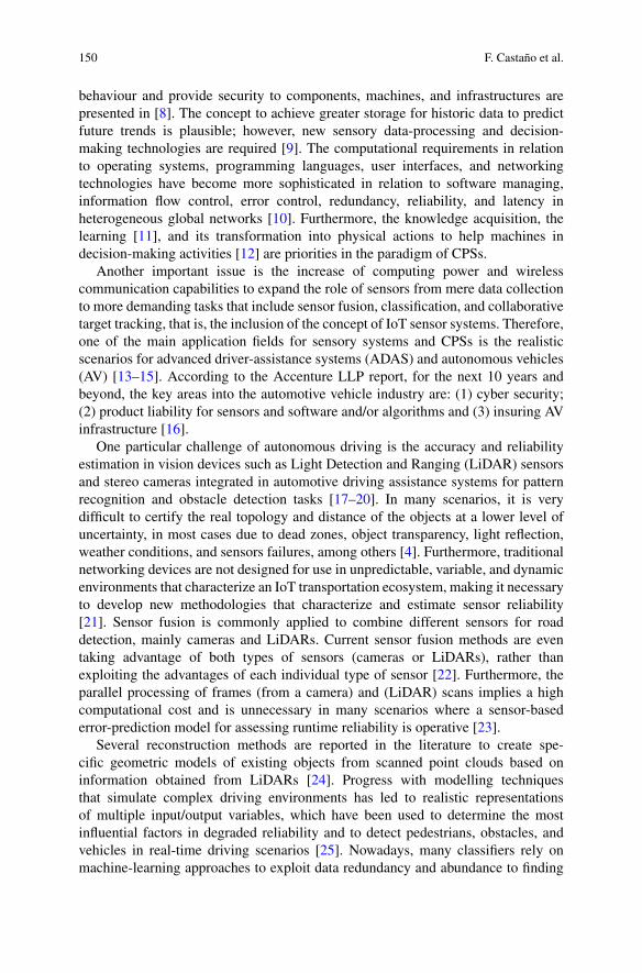
150 F. Castaño et al.
behaviour and provide security to components, machines, and infrastructures arepresented in [8]. The concept to achieve greater storage for historic data to predictfuture trends is plausible; however, new sensory data-processing and decision-making technologies are required [9]. The computational requirements in relationto operating systems, programming languages, user interfaces, and networkingtechnologies have become more sophisticated in relation to software managing,information flow control, error control, redundancy, reliability, and latency inheterogeneous global networks [10]. Furthermore, the knowledge acquisition, thelearning [11], and its transformation into physical actions to help machines indecision-making activities [12] are priorities in the paradigm of CPSs.
Another important issue is the increase of computing power and wirelesscommunication capabilities to expand the role of sensors from mere data collectionto more demanding tasks that include sensor fusion, classification, and collaborativetarget tracking, that is, the inclusion of the concept of IoT sensor systems. Therefore,one of the main application fields for sensory systems and CPSs is the realisticscenarios for advanced driver-assistance systems (ADAS) and autonomous vehicles(AV) [13–15]. According to the Accenture LLP report, for the next 10 years andbeyond, the key areas into the automotive vehicle industry are: (1) cyber security;(2) product liability for sensors and software and/or algorithms and (3) insuring AVinfrastructure [16].
One particular challenge of autonomous driving is the accuracy and reliabilityestimation in vision devices such as Light Detection and Ranging (LiDAR) sensorsand stereo cameras integrated in automotive driving assistance systems for patternrecognition and obstacle detection tasks [17–20]. In many scenarios, it is verydifficult to certify the real topology and distance of the objects at a lower level ofuncertainty, in most cases due to dead zones, object transparency, light reflection,weather conditions, and sensors failures, among others [4]. Furthermore, traditionalnetworking devices are not designed for use in unpredictable, variable, and dynamicenvironments that characterize an IoT transportation ecosystem, making it necessaryto develop new methodologies that characterize and estimate sensor reliability[21]. Sensor fusion is commonly applied to combine different sensors for roaddetection, mainly cameras and LiDARs. Current sensor fusion methods are eventaking advantage of both types of sensors (cameras or LiDARs), rather thanexploiting the advantages of each individual type of sensor [22]. Furthermore, theparallel processing of frames (from a camera) and (LiDAR) scans implies a highcomputational cost and is unnecessary in many scenarios where a sensor-basederror-prediction model for assessing runtime reliability is operative [23].
Several reconstruction methods are reported in the literature to create spe-cific geometric models of existing objects from scanned point clouds based oninformation obtained from LiDARs [24]. Progress with modelling techniquesthat simulate complex driving environments has led to realistic representationsof multiple input/output variables, which have been used to determine the mostinfluential factors in degraded reliability and to detect pedestrians, obstacles, andvehicles in real-time driving scenarios [25]. Nowadays, many classifiers rely onmachine-learning approaches to exploit data redundancy and abundance to finding
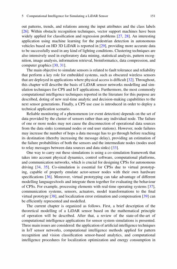
5 Computational Intelligence for Simulating a LiDAR Sensor 151
out patterns, trends, and relations among the input attributes and the class labels[26]. Within obstacle recognition techniques, vector support machines have beenwidely applied for classification and regression problems [27, 28]. An interestingapplication using machine learning for the pedestrian detection in autonomousvehicles based on HD 3D LiDAR is reported in [29], providing more accurate datato be successfully used in any kind of lighting conditions. Clustering techniques arealso intensively used in exploratory data mining, statistical analysis, pattern recog-nition, image analysis, information retrieval, bioinformatics, data compression, andcomputer graphics [30, 31].
The main objective to simulate sensors is related to fault tolerance and reliabilitythat perform a key role for embedded systems, such as obscured wireless sensorsthat are deployed in applications where physical access is difficult [32]. Throughout,this chapter will describe the basis of LiDAR sensor networks modelling and sim-ulation techniques for CPS and IoT applications. Furthermore, the most commonlycomputational intelligence techniques reported in the literature for this purpose aredescribed, doting of new real-time analytic and decision-making capabilities to thenext sensor generations. Finally, a CPS use case is introduced in order to deploy atechnical application scenario.
Reliable monitoring of a phenomenon (or event detection) depends on the set ofdata provided by the cluster of sensors rather than any individual node. The failureof one or more nodes may not cause the disconnection of operational data sourcesfrom the data sinks (command nodes or end user stations). However, node failuresmay increase the number of hops a data message has to go through before reachingits destination (thereby increasing the message delay), providing an estimation ofthe failure probabilities of both the sensors and the intermediate nodes (nodes usedto relay messages between data sources and data sinks) [33].
One way to carry out these simulations is using a co-simulation framework thattakes into account physical dynamics, control software, computational platforms,and communication networks, which is crucial for designing CPSs for autonomousdriving [34, 35]. Co-simulation is essential for CPSs due to virtual prototyp-ing, capable of properly emulate actor-sensor nodes with their own hardwarespecifications [36]. Moreover, virtual prototyping can take advantage of differentmodelling languages/tools and integrate them together for evaluating the behaviourof CPSs. For example, processing elements with real-time operating systems [37],communication systems, sensors, actuators, model transformations to the finalvirtual prototype [38], and localization error estimation and compensation [39] canbe efficiently represented and modelled.
The current chapter is organized as follows. First, a brief description of thetheoretical modelling of a LiDAR sensor based on the mathematical principleof operation will be described. After that, a review of the state-of-the-art ofcomputational intelligence applications for sensor system simulations is presented.Three main issues are considered: the application of artificial intelligence techniquesin IoT sensor networks, computational intelligence methods applied for patternrecognition and vision classification sensor-based analytics, and computationalintelligence procedures for localization optimization and energy consumption in
152 F. Castaño et al.
sensor networks. Next, a real case study of artificial intelligence techniques appliedto sensor networks in a Cyber-Physical System is presented. Finally, the conclusionsand future research steps are summarized.
5.2 Theoretical Modelling of a LiDAR Sensor
LiDAR, also frequently referred to as Laser Detection and Ranging (LiDAR),uses a laser to produce light pulses. LiDAR maintains some similitudes with itspredecessor, Radio Detection and Ranging (RADAR), with the main deferencebeing that it is carried out with electromagnetic radiation at a much smallerwavelength and greater frequency. Both technologies are based on Time-of-Flight(ToF) for the light pulses. In addition, light velocity allows these sensors to takenumerous measurements per second [40].
Depending on the principle of operation and the ability to reconstruct or interpreta scanned scene from the data provided by these sensors can be classified in: singlepoint and imaging. The first uses a single laser and photodetector such that thespatial information is limited to a single point in the propagation direction. Instead,the second is able to reconstruct or interpret a scanned 2D or 3D scene. This can becarried out by adding a scanning laser system to the single point LiDAR sensorso that it will rasterize an image normal to the propagation direction. Anotherimaging method uses an array of photodetectors to obtain the temporal and spatialinformation with each pulse of laser energy. Though they are able to gain spatialinformation using an array of photodetectors, there is often a need for scanningthe scene in order to obtain a detailed image [41]. Multiple sources and multipledetectors is also an option for imaging with LiDAR. In the case of weak signals, evensingle photon detection can be achieved using a Geiger-mode avalanche photodiode(GmAPD) [42] for either single point or imaging systems [43]. Figure 5.1 shows thetwo distributions for the laser pulse travelling from the LiDAR system to the target,where Δr is the aperture diameter of the receiver, θ fov is the angle of vertical fieldof view, and R is range dimension in the direction of the pulse travelling.
In the subsequent sections, mathematical models are carried out, consideringautomotive application’s constraints.
5.2.1 Laser Beam Model
The intensity of the laser beam across the range is not uniform, but varies in thespatial and temporal domains [42]. It is defined as a beam profile and depends onthe shape of the emitter and the technique used to generate the laser light. Generally,this profile or energy distribution is modelled as a spatial Gaussian function of radiusr from the centre of the beam spot and distance z from the aperture [40]:
5 Computational Intelligence for Simulating a LiDAR Sensor 153
Fig. 5.1 The division of the process during simulation. Figure adapted from [40, 41, 44]
I (r, z) = I0 ·(
ω0
ω(z)
)2
· e
(−2·r2
ω2(z)
)
(5.1)
where ω0 = λ (π Θ) is the beam width (radius) of the pulse at z = 0 also known asthe beam waist [45].
The radial distance (in m) at which the profile value is decreased to 1/e2 from itspeak value is zr = πω0 /λ, where λ is the laser wavelength.
The value of I0 is found by integrating Eq. (5.1) over r and setting the result equalto the laser power, P.
I0 = 2 · P
π · ω20
(5.2)
In addition, Eq. (5.3) represents the free space propagation of the beam results indivergence of the beam width, ω(z), where z is the propagation distance. This is truefor distances that are less than the Rayleigh length [45].
ω(z) = ω0
√
1 +(
z
zr
)2
(5.3)
In the temporal domain, the laser signal is modelled as a pulse. There are severalpulse models with different shapes. The time propagation for a typical laser pulsecan be described by:
p(t) =(
t
τ
)2
· e− tτ , where τ = T1/2
3.5, (5.4)
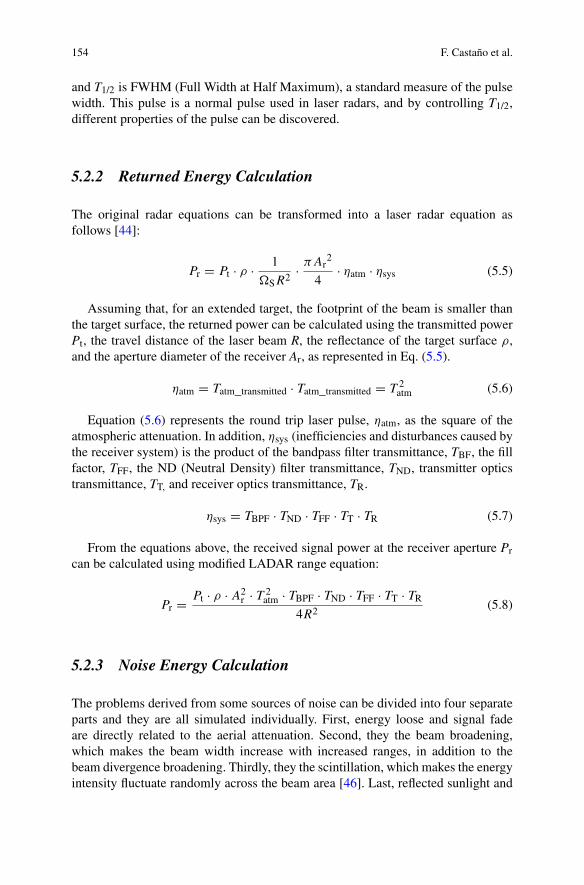
154 F. Castaño et al.
and T1/2 is FWHM (Full Width at Half Maximum), a standard measure of the pulsewidth. This pulse is a normal pulse used in laser radars, and by controlling T1/2,different properties of the pulse can be discovered.
5.2.2 Returned Energy Calculation
The original radar equations can be transformed into a laser radar equation asfollows [44]:
Pr = Pt · ρ · 1
�SR2 · πAr2
4· ηatm · ηsys (5.5)
Assuming that, for an extended target, the footprint of the beam is smaller thanthe target surface, the returned power can be calculated using the transmitted powerPt, the travel distance of the laser beam R, the reflectance of the target surface ρ,and the aperture diameter of the receiver Ar, as represented in Eq. (5.5).
ηatm = Tatm_transmitted · Tatm_transmitted = T 2atm (5.6)
Equation (5.6) represents the round trip laser pulse, ηatm, as the square of theatmospheric attenuation. In addition, ηsys (inefficiencies and disturbances caused bythe receiver system) is the product of the bandpass filter transmittance, TBF, the fillfactor, TFF, the ND (Neutral Density) filter transmittance, TND, transmitter opticstransmittance, TT, and receiver optics transmittance, TR.
ηsys = TBPF · TND · TFF · TT · TR (5.7)
From the equations above, the received signal power at the receiver aperture Prcan be calculated using modified LADAR range equation:
Pr = Pt · ρ · A2r · T 2
atm · TBPF · TND · TFF · TT · TR
4R2 (5.8)
5.2.3 Noise Energy Calculation
The problems derived from some sources of noise can be divided into four separateparts and they are all simulated individually. First, energy loose and signal fadeare directly related to the aerial attenuation. Second, they the beam broadening,which makes the beam width increase with increased ranges, in addition to thebeam divergence broadening. Thirdly, they the scintillation, which makes the energyintensity fluctuate randomly across the beam area [46]. Last, reflected sunlight and
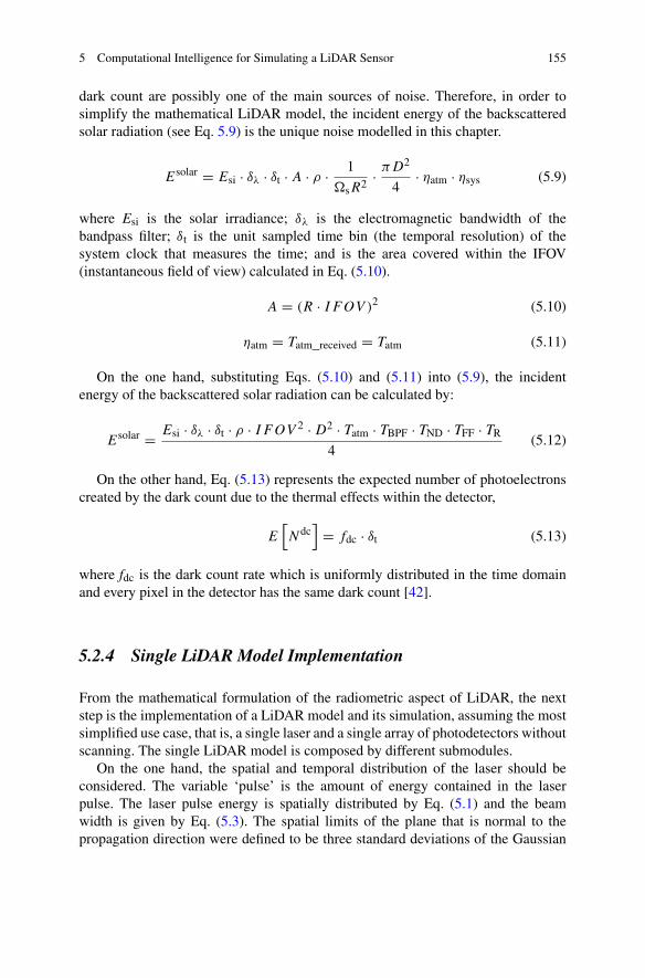
5 Computational Intelligence for Simulating a LiDAR Sensor 155
dark count are possibly one of the main sources of noise. Therefore, in order tosimplify the mathematical LiDAR model, the incident energy of the backscatteredsolar radiation (see Eq. 5.9) is the unique noise modelled in this chapter.
Esolar = Esi · δλ · δt · A · ρ · 1
�sR2· πD2
4· ηatm · ηsys (5.9)
where Esi is the solar irradiance; δλ is the electromagnetic bandwidth of thebandpass filter; δt is the unit sampled time bin (the temporal resolution) of thesystem clock that measures the time; and is the area covered within the IFOV(instantaneous field of view) calculated in Eq. (5.10).
A = (R · IFOV )2 (5.10)
ηatm = Tatm_received = Tatm (5.11)
On the one hand, substituting Eqs. (5.10) and (5.11) into (5.9), the incidentenergy of the backscattered solar radiation can be calculated by:
Esolar = Esi · δλ · δt · ρ · IFOV 2 · D2 · Tatm · TBPF · TND · TFF · TR
4(5.12)
On the other hand, Eq. (5.13) represents the expected number of photoelectronscreated by the dark count due to the thermal effects within the detector,
E[Ndc
]= fdc · δt (5.13)
where fdc is the dark count rate which is uniformly distributed in the time domainand every pixel in the detector has the same dark count [42].
5.2.4 Single LiDAR Model Implementation
From the mathematical formulation of the radiometric aspect of LiDAR, the nextstep is the implementation of a LiDAR model and its simulation, assuming the mostsimplified use case, that is, a single laser and a single array of photodetectors withoutscanning. The single LiDAR model is composed by different submodules.
On the one hand, the spatial and temporal distribution of the laser should beconsidered. The variable ‘pulse’ is the amount of energy contained in the laserpulse. The laser pulse energy is spatially distributed by Eq. (5.1) and the beamwidth is given by Eq. (5.3). The spatial limits of the plane that is normal to thepropagation direction were defined to be three standard deviations of the Gaussian
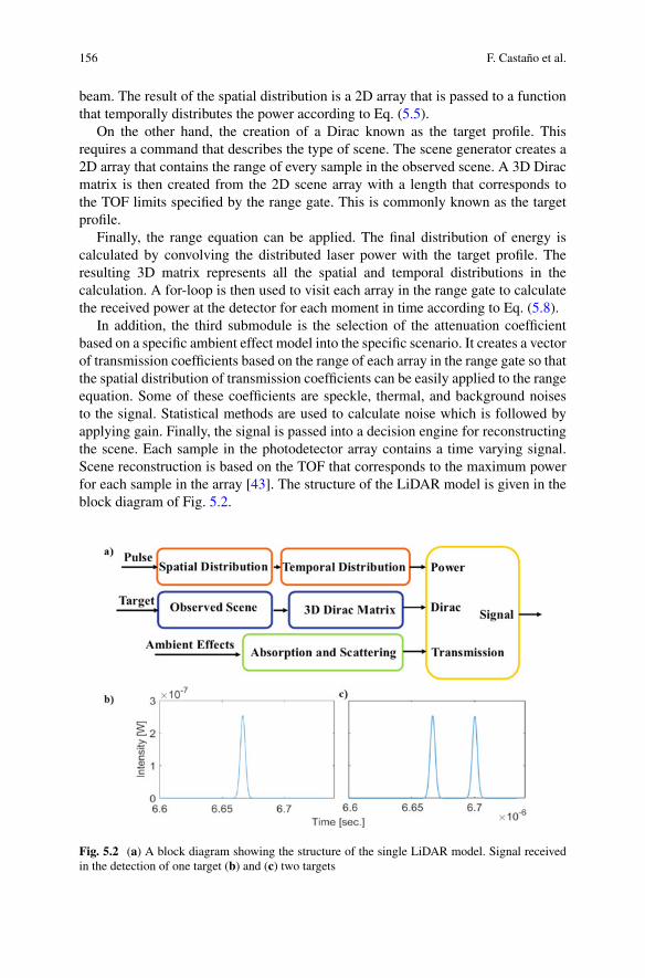
156 F. Castaño et al.
beam. The result of the spatial distribution is a 2D array that is passed to a functionthat temporally distributes the power according to Eq. (5.5).
On the other hand, the creation of a Dirac known as the target profile. Thisrequires a command that describes the type of scene. The scene generator creates a2D array that contains the range of every sample in the observed scene. A 3D Diracmatrix is then created from the 2D scene array with a length that corresponds tothe TOF limits specified by the range gate. This is commonly known as the targetprofile.
Finally, the range equation can be applied. The final distribution of energy iscalculated by convolving the distributed laser power with the target profile. Theresulting 3D matrix represents all the spatial and temporal distributions in thecalculation. A for-loop is then used to visit each array in the range gate to calculatethe received power at the detector for each moment in time according to Eq. (5.8).
In addition, the third submodule is the selection of the attenuation coefficientbased on a specific ambient effect model into the specific scenario. It creates a vectorof transmission coefficients based on the range of each array in the range gate so thatthe spatial distribution of transmission coefficients can be easily applied to the rangeequation. Some of these coefficients are speckle, thermal, and background noisesto the signal. Statistical methods are used to calculate noise which is followed byapplying gain. Finally, the signal is passed into a decision engine for reconstructingthe scene. Each sample in the photodetector array contains a time varying signal.Scene reconstruction is based on the TOF that corresponds to the maximum powerfor each sample in the array [43]. The structure of the LiDAR model is given in theblock diagram of Fig. 5.2.
Fig. 5.2 (a) A block diagram showing the structure of the single LiDAR model. Signal receivedin the detection of one target (b) and (c) two targets
5 Computational Intelligence for Simulating a LiDAR Sensor 157
5.3 Computational Intelligence Applications in SensorSystem Simulations
5.3.1 Application of Artificial Intelligence Techniques in IoTSensor Networks
IoT sensor networks require the integration of relevant stages such as: identifying,sensing, networking, and computation. These networks enable large scale of techno-logical innovations and value-added services which personalize user’s interaction.There are numerous IoT applications that can be grouped into various domains suchas health, traffic, logistics, retail, agriculture, smart cities, smart metering, remotemonitoring, process automation, among others. Despite the enormous progress indifferent research fields including architectures, standardization, emerging technolo-gies, security, etc. [47]. Wireless Sensor Networks (WSN) can be used to measureand track of energy consumption and production in order to optimize energyusage. In general, IoT communication is performed by producing and consuminginformation and by executing smart algorithms to interact intelligently with otherthings. The main challenges in the implementation of WSN in IoT are:
• Deployment• Quality of service• Localization• Energy consumption• Data collection and transmission• Mobility management
In order to deal with some these challenges, new communications, protocols,and tools are reported in literature, highlighting the use of artificial intelligencetechniques [48] in particular machine-learning algorithms (ML) to solve complexsituation in sensor network scenarios. Artificial intelligence (AI) techniques provideto WSNs cognitive abilities in order to improve its performance by reducing powerconsumption, increasing network lifetime, reliability, and also in general enhancingquality of service (QoS) through the processing of great amount of data obtainedfrom environment monitoring and applying optimization in order to determine thebest parameters [49].
By the other hand, the fault detection is a key issue in autonomous systems.The main reason is that fault detection enables the systems to self-correct problemssuch as data package lost, determine data collision, the status of the element of thenetwork, among others. The presence of faults in wireless sensor data may increasethe network traffic and wastes the battery and power. Several techniques can be usedsuch as nearest neighbour methods, and other clustering techniques for providingthe system capabilities of self-adjust and data lost detection and correction [50].Constructing real-time prediction models are important to maximize the networklifetime meanwhile guaranteeing connectivity and robustness [51]. The design ofadaptive and intelligent WSN is essential. The adaptation and self-organization
158 F. Castaño et al.
capabilities can be introduced through embedding artificial neural networks in thecontrol systems of the WSNs providing reliability [52].
Sensor reliability is one of the main challenges found in IoT applications dueto the need to ensure the correct monitoring of the process in order to ensure thatthe operation is within limits imposed. Since the sensor output is the only objectivesource of information of the status of the environment for decision-making, it isessential that the operating status of the sensors be known. The performance ofonline monitoring and self-correction of multiple sensors, through the applicationof some ML algorithms such as support vector machine (SVM) and ANNs, is veryimportant to reduce maintenance costs, minimize the risk of using uncalibrated orfaulty sensors, increase instrument reliability, and consequently increase equipmentlife [53, 54].
The network dynamics is another very important aspect to take into considerationinto the sensor networks and IoT infrastructures. The interaction between theelements of the network can be determined by the performance of the network andit is critical to ensure its correct function. The development of scheduling strategiesto ensure the coverage of points in wireless sensor networks is essential in order tooptimize the sequence of states and increase the lifetime of the network, consideringthe resource scarcity and address the network dynamism. Techniques such asHidden Markov Model present great performance in the scheduling design allowingthe optimization of the lifetime without decrease in the network performance [55].
Protocols are also an important aspect to consider in the design of robust WSNs.The correct design of protocols has a great influence in the energy consumption,data congestion, and in general the performance of the system. As the limited powerof the sensors is one of the main challenges energy save is vital to ensure a correctoperation of the system. The design of protocols with low power approach alongwith the uses of ANNs facilitate local processing allowing faster responses as wellas improve overall system efficiency and power saving [56]. In order to detectcongestion the uses of algorithms like SVM to predict the level of congestion ofthe system allows the accurate adjustment of data transmission rate in each wirelesssensor node which leads to a balanced traffic [57].
5.3.2 Computational Intelligence Applied in PatternRecognition and Vision Classification Sensor-BasedAnalytics
Nowadays, several challenges arise from the sensor fusion, real-time and on-boardimplementation on sensor networks motivated by the need of new functionalitiessuch as: data pre-processing, advanced analytics, pattern recognition, and classi-fication actions based on the collection of huge amount of data points become aproblem to be considered for current and future sensor manufactures, providers, andresearchers [58, 59].
5 Computational Intelligence for Simulating a LiDAR Sensor 159
In particular, human activities recognition is an important research topic inthe new IoT era, in order to analyse the behaviour and improve the human–computer interactions. In the last decades, different computational intelligencetechniques have demonstrated their suitability to optimize industrial processes [60,61]. In particular, artificial neural networks and fuzzy systems have been worldwideapplied [62–64]. Nowadays, the increase of human–machine interactions will beone of the biggest challenges for the industry and society of the future, becomingthe sensors first key element of this interaction [65]. Based on that, multiplestudies are focused on the recognition of daily activities as an essential issue formaintaining healthy lifestyle, patient rehabilitation, and activity shifts among theelderly citizens, detecting and diagnosing serious illness patterns [66]. One exampleof that, it is the use of sensor data generated by smartphones and other wearabledevices in order to dominate the research landscape in human motion analysis,activity monitoring, and detection due to their obvious advantages over other sensormodalities [67]. Recently, to overcome the challenges associated with single sensormodalities and increase generalization, many studies have proposed informationfusion strategies that combine multiple sensors modalities or classifiers to increaserobustness, reliabilities, derive confidence measures among different classifiers andreduce the complexity of recognition system [68]. Information fusion in humanactivity recognition is necessitated by increase in sensor of different modalities[69]. Information fusion techniques are prevalent in both handcrafted features andautomatic feature learning using deep learning algorithms [70].
Deep learning algorithms are applied on sensor data to extract discriminative andsalient features and then flattened and passed to an inference engine to recognizeactivities classes [71]. In this field, recently applications focused on pedestrianretrieval via part-based gradation regularization in sensor networks were reportedby [72]. The solution proposes a novel part-based gradation regularization methodto assign a pedestrian label for each horizontal part. For that, it has been combinedthe strengths of the local convolutional neural network (CNN) with an identificationembedding model to extract and classify the main features. The results describedin the approach not only validate the high accuracy to learn from the localfeatured based on CNN, they also demonstrate and improve the generalizationability of the classification model to mitigate the risk of overfitting and increasethe performance of pedestrian retrieval due to rational utilization of pedestrianlabels. Nevertheless, other traditional machine-learning classifiers such as: supportvector machine [73], k-nearest neighbours [74], multinomial regressions [74], andHidden Markov Models [75] are still highly used in pattern recognition and dataclassification applications.
On the other hand, intelligent transport systems (ITS) highly impact researchtopic in recent years. The possibility to provide innovative services relating todifferent modes of transport and traffic management and enabling various usersto be better informed and make safer, more coordinated, and ‘smarter’ use oftransport networks is very promising. ITS aim to improve transportation safety,mobility, productivity, and environmental performance for traffic planners androad users. With continuous urban road development and extensive construction
160 F. Castaño et al.
of expressways, increasing interest is devoted to vehicle detection [76]. Into thistransformation, the new generation of sensors, the sensor fusion, sensor network,and IoT-based solutions get an important role in function to collect real-time datafrom the billions of devices present in the smart mobility ecosystems [77].
One example of that is reported by [78], with the purpose to improve the real-timeperformance and accuracy of vehicle type recognition in complex traffic scenes.For a single vehicle, data collected from A and B nodes have a certain temporaland spatial correlation, and the signals can be enhanced and fused in the lateranalysis. Based on this estimation, the authors have developed a multiple sensorsinformation fusion method, which consists of the following key components: datasegmentation and filtering, vehicle feature matching, and vehicle feature waveformfusion. Finally, the experimental results obtained by the proposed method describesa 95% accuracy for small vehicles (tourism) and 90% accuracy for large vehicles(buses) approximately, becoming a key issue to provide references for multiplesensor network design and traffic data collection. Other recent example is the noveltechnique presented by [79] to apply a harmony search evolutionary algorithmin real-time line detection vision based on a two-wheeled robotic platform. Theproposed vision-based algorithm is implemented to process the images capturedfrom on-board camera allowed in a two-wheeled robot, follows the path via on-board microcontroller governing motors. The proposed system is able to detect andfollow the path with 99% accuracy, regardless of image size and eliminates edgedetection phase altogether. These are only two examples of the true potentialitiesof the computational intelligence-based solutions based on sensor data collectionto extract the main feature of complex dynamic environments, model the potentialactions and risk, and to facilitate the decision-making process for human andvehicles. The near future will demand fast solution in unknown situations, becomingthe sensor reliability one of the most important attribute to be considered during thedesign, implemenation and performance of the future sensor networks.
5.3.3 Computational Intelligence Applied in LocalizationOptimization and Energy Consumption in SensorNetworks
Sensors are a crucial component in every intelligent control system [80]. Wirelesssensor networks (WSNs) are one of the most rapidly developing informationtechnologies and promise to have a variety of applications in Next GenerationNetworks, Internet-of-Things (IoT), becoming the sensor reliability one of themost important attribute to be considered during the design, implementation andperformance of the future sensor networks [81].
Most WSNs reliability assessments are based on graph theory and probabilitytheory. Connectivity reliability investigates the probability that the network is stillconnected for a given period of time under the case of some nodes or links failure.
5 Computational Intelligence for Simulating a LiDAR Sensor 161
Performance reliability analyses the end-to-end delay, packet delivery rate, and othernetwork parameters [82, 83].
WSNs reliability is influenced by many factors such as component failure,environmental influences, task changes, and network update. These factors andnetwork behaviour are difficult to be described or calculated by mathematicalmodels. Network simulation becomes an important method to analyse networkreliability [84]. Based on that, the objective of this subsection is to analyse compu-tational intelligence-based implantations reported in the literature to contribute onthe sensor networks reliability. Following, four main topics were selected based onnode localization, energy management, network multi-objective optimization, andself-capabilities approach to describe the impact of the computational intelligencetechniques into the present and future sensor networks [85, 86].
The emergence IoT-based applications are revolutionizing the current concept ofindustry, transportation systems, energy grids, cities, and society [87]. To archivethis transformation, many daily applications based on IoT require an efficient nodeposition and localization mechanism [88, 89]. Localization technology has been acore component for Internet-of-Things, especially for Wireless Sensor Network.
On the one hand, the localization techniques range-based are based on measuringthe distance or the angle between the directions of reference nodes called anchors.Several technologies allow the nodes distance measure such as: Received SignalStrength Indicator [90], Time of Arrival [91], Time Difference of Arrival [92],and Angle of Arrival [93], among others. On the other hand, range-free-basedlocalization solutions can avoid the increase of the energy consumption and theinappropriate cost of the equipment. Range-free technologies introduce an inde-pendence between the hardware devices and the distance computing [94]. Hence,this independence allows the adaption technology of different wireless transmissiontypes based on locations as centroid, Approximate Point in Triangle Test [95]and Distance Vector-Hop (DV-Hop) [95]. Although these algorithms provide moreeconomic and simple estimations, their results are not as accurate as tracking errorlevel. A precise detection of the transmitter node position allows an effective routingof information with minimum energy consumption. Another important parameter isthe localization time which is the necessary time for the network localization [96].Nevertheless, range-free algorithms have relatively lower localization accuracy, butit is more widespread to be used because of the inexpensive cost and simplicity,especially in the large-scale network [97].
In this topic, an interesting result is introduced by [98], developing a novelhigh accurate localization algorithm based on DV-Hop and differential evolution(DECHDV-Hop) for WSN. In particular, DECHDV-Hop improves the positioningaccuracy without adding extra equipment to the sensor network. In order to furtherreduce the localization error, DE algorithm is used to locate unknown nodesby formulating the location estimation process as an optimization problem. Theobtained results show a reduction in the average localization error about 70%compared with traditional DV-Hop techniques in the simulation of four differentnetwork situations (Random, Grid, C-shaped random, and C-shaped grid). Theaverage localization error was estimated based on the following equation:
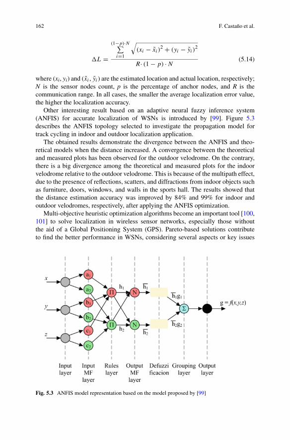
162 F. Castaño et al.
L =
(1−p)·N∑i=1
√(xi − xi )
2 + (yi − yi )2
R· (1 − p) ·N (5.14)
where (xi, yi) and (xi , yi) are the estimated location and actual location, respectively;N is the sensor nodes count, p is the percentage of anchor nodes, and R is thecommunication range. In all cases, the smaller the average localization error value,the higher the localization accuracy.
Other interesting result based on an adaptive neural fuzzy inference system(ANFIS) for accurate localization of WSNs is introduced by [99]. Figure 5.3describes the ANFIS topology selected to investigate the propagation model fortrack cycling in indoor and outdoor localization application.
The obtained results demonstrate the divergence between the ANFIS and theo-retical models when the distance increased. A convergence between the theoreticaland measured plots has been observed for the outdoor velodrome. On the contrary,there is a big divergence among the theoretical and measured plots for the indoorvelodrome relative to the outdoor velodrome. This is because of the multipath effect,due to the presence of reflections, scatters, and diffractions from indoor objects suchas furniture, doors, windows, and walls in the sports hall. The results showed thatthe distance estimation accuracy was improved by 84% and 99% for indoor andoutdoor velodromes, respectively, after applying the ANFIS optimization.
Multi-objective heuristic optimization algorithms become an important tool [100,101] to solve localization in wireless sensor networks, especially those withoutthe aid of a Global Positioning System (GPS). Pareto-based solutions contributeto find the better performance in WSNs, considering several aspects or key issues
Fig. 5.3 ANFIS model representation based on the model proposed by [99]
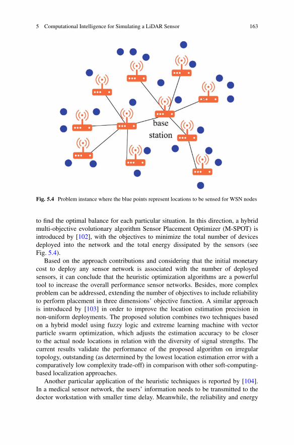
5 Computational Intelligence for Simulating a LiDAR Sensor 163
Fig. 5.4 Problem instance where the blue points represent locations to be sensed for WSN nodes
to find the optimal balance for each particular situation. In this direction, a hybridmulti-objective evolutionary algorithm Sensor Placement Optimizer (M-SPOT) isintroduced by [102], with the objectives to minimize the total number of devicesdeployed into the network and the total energy dissipated by the sensors (seeFig. 5.4).
Based on the approach contributions and considering that the initial monetarycost to deploy any sensor network is associated with the number of deployedsensors, it can conclude that the heuristic optimization algorithms are a powerfultool to increase the overall performance sensor networks. Besides, more complexproblem can be addressed, extending the number of objectives to include reliabilityto perform placement in three dimensions’ objective function. A similar approachis introduced by [103] in order to improve the location estimation precision innon-uniform deployments. The proposed solution combines two techniques basedon a hybrid model using fuzzy logic and extreme learning machine with vectorparticle swarm optimization, which adjusts the estimation accuracy to be closerto the actual node locations in relation with the diversity of signal strengths. Thecurrent results validate the performance of the proposed algorithm on irregulartopology, outstanding (as determined by the lowest location estimation error with acomparatively low complexity trade-off) in comparison with other soft-computing-based localization approaches.
Another particular application of the heuristic techniques is reported by [104].In a medical sensor network, the users’ information needs to be transmitted to thedoctor workstation with smaller time delay. Meanwhile, the reliability and energy
164 F. Castaño et al.
consumption are necessary to be considered. To archive this goal, the authorsconsidered the smaller time delay, high reliability to transfer information, andprolong the lifetime of the node simultaneously as objective functions. For that,a differential evolution was selected to optimize the smaller delay time needs sensornetwork quickly process and transmit the data, as well as, to increase the reliabilityto reduce the probability of false or loss package. An interesting result introduced bythe current approach is focused on the relationship between increment of reliabilitywith the delay and energy consumption. These parameters have clear conflictsbetween each other into the sensor network infrastructures. Otherwise, prolongingthe lifetime of the node needs to consider the energy consumption and residualenergy, and then try to choose more residual energy of nodes involved in informationtransmission.
Most applications of WSN require that the sensor nodes must be aware of theirlocation relative to the SN. For this, one of the important challenges in WSN is thelocalization of sensor nodes and determination of nodes positions in the sensor field[105]. As it was commented before, in the case of sensor networks, the energy isother key performance indicator of efficiency and reliability values. For this, GPSdevices are not convenient as valid solution of localization problem in WSN formany reasons [106]:
• Once the expensive GPS devices are added to every sensor node in the network,this solution becomes unfeasible due to the increase of the deployment cost.
• With the inclusion of GPS device the sensor nodes size becomes quite large,limiting the required properties of WSN where nodes should be designed in smallsize.
• To work property, GPS devices always depend on satellites information. In casesof failure with satellite link, GPS ceases to function. It is the case of many realapplications as indoor and explorative applications.
• Finally, GPS in WSN depend on many factors such as: power consumption, cost,and size, being not the case of other localization techniques.
In order to sustain long-term sensing capability over a large coverage set, theenergy conservation becomes an important factor to extend the battery life in sensornetworks. Replacement of a node battery is infeasible due to the harsh environmentin which the sensor networks are usually deployed in [107], becoming an imperativeissue to prioritize energy efficiency in order to maximize network lifetime andperformance. In time-critical applications, routing delay also becomes a pressingfactor [108]. In order to address the energy consumption issue effectively, theenergy-efficient grid-based routing algorithm introduced by [109] overcomes thehotspot problem and utilizes the energy of nodes more efficiently. This algorithmconsists of three different phases, namely, grid formation, grid coordinator election,and grid-based routing phases. For that, each grid is elected by applying fuzzy logicwhere the fuzzy variables are used for grid coordination selection based on theresidual energy of the nodes, their mobility pattern, and the distance of the nodesfrom the sink node. As the transmission consumes energy based on the distance, the
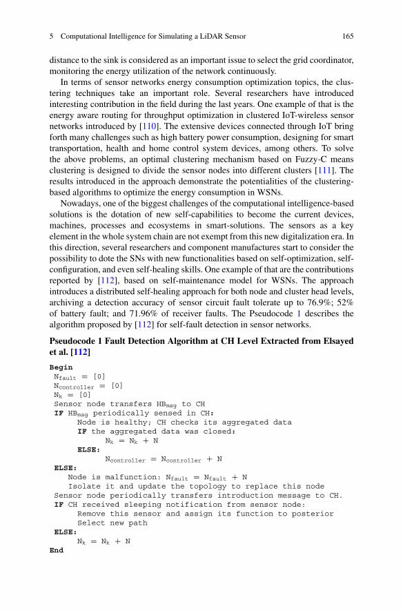
5 Computational Intelligence for Simulating a LiDAR Sensor 165
distance to the sink is considered as an important issue to select the grid coordinator,monitoring the energy utilization of the network continuously.
In terms of sensor networks energy consumption optimization topics, the clus-tering techniques take an important role. Several researchers have introducedinteresting contribution in the field during the last years. One example of that is theenergy aware routing for throughput optimization in clustered IoT-wireless sensornetworks introduced by [110]. The extensive devices connected through IoT bringforth many challenges such as high battery power consumption, designing for smarttransportation, health and home control system devices, among others. To solvethe above problems, an optimal clustering mechanism based on Fuzzy-C meansclustering is designed to divide the sensor nodes into different clusters [111]. Theresults introduced in the approach demonstrate the potentialities of the clustering-based algorithms to optimize the energy consumption in WSNs.
Nowadays, one of the biggest challenges of the computational intelligence-basedsolutions is the dotation of new self-capabilities to become the current devices,machines, processes and ecosystems in smart-solutions. The sensors as a keyelement in the whole system chain are not exempt from this new digitalization era. Inthis direction, several researchers and component manufactures start to consider thepossibility to dote the SNs with new functionalities based on self-optimization, self-configuration, and even self-healing skills. One example of that are the contributionsreported by [112], based on self-maintenance model for WSNs. The approachintroduces a distributed self-healing approach for both node and cluster head levels,archiving a detection accuracy of sensor circuit fault tolerate up to 76.9%; 52%of battery fault; and 71.96% of receiver faults. The Pseudocode 1 describes thealgorithm proposed by [112] for self-fault detection in sensor networks.
Pseudocode 1 Fault Detection Algorithm at CH Level Extracted from Elsayedet al. [112]
BeginNfault = [0]Ncontroller = [0]Nk = [0]Sensor node transfers HBmsg to CHIF HBmsg periodically sensed in CH:
Node is healthy; CH checks its aggregated dataIF the aggregated data was closed:
Nk = Nk + NELSE:
Ncontroller = Ncontroller + NELSE:
Node is malfunction: Nfault = Nfault + NIsolate it and update the topology to replace this node
Sensor node periodically transfers introduction message to CH.IF CH received sleeping notification from sensor node:
Remove this sensor and assign its function to posteriorSelect new path
ELSE:Nk = Nk + N
End
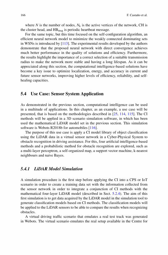
166 F. Castaño et al.
where N is the number of nodes, Nk is the active vertices of the network, CH isthe cluster head, and HBmsg is periodic heartbeat message.
For the same topic, but this time focused on the self-configuration algorithm, anefficient neural network model to minimize the weakly connected dominating setsin WSNs is introduced by [113]. The experimental results developed by the authorsdemonstrate that the proposed neural network with direct convergence achievesmuch better performance in the quality of solutions and efficiency. Furthermore,the results highlight the importance of a correct selection of a suitable transmissionradius to make the network more stable and having a long lifespan. As it can beappreciated along this section, the computational intelligence-based solutions havebecome a key issue to optimize localization, energy, and accuracy in current andfuture sensor networks, improving higher levels of efficiency, reliability, and self-healing capacities.
5.4 Use Case: Sensor System Application
As demonstrated in the previous section, computational intelligence can be usedin a multitude of applications. In this chapter, as an example, a use case will bepresented, that is based on the methodologies described in [25, 114, 115]. The CImethods will be applied in a 3D scenario simulation software, in which has beenused the mathematical LiDAR model set in the previous section. This simulationsoftware is Webots R2018b for automobiles [116].
The purpose of this use case is apply a CI model library of object classificationusing the LiDAR data in a virtual sensor network in a Cyber-Physical System toobstacle recognition in driving assistance. For this, four artificial intelligence-basedmethods and a probabilistic method for obstacle recognition are explored, such asa multi-layer perceptron, a self-organized map, a support vector machine, k-nearestneighbours and naive Bayes.
5.4.1 LiDAR Model Simulation
A simulation procedure is the first step before applying the CI into a CPS or IoTscenario in order to create a training data set with the information collected fromthe sensor network in order to integrate a conjunction of CI methods with themathematical four-layer LiDAR model (described in Sect. 5.2.4). The aim of thisfirst simulation is to get data acquired by the LiDAR model in the simulation tool togenerate classification models based on CI methods. The classification models willbe applied to the LiDAR sensors to be able to compare the results when recognizingobstacles.
A virtual driving traffic scenario that emulates a real test track was generatedin Webots. The virtual scenario emulates the real setup available in the Centre for
5 Computational Intelligence for Simulating a LiDAR Sensor 167
Fig. 5.5 Aerial view of the (a) real and (b) 3D simulated scenario, with a real and modelled vehiclewith sensors incorporated
Automation and Robotics (CAR-CSIC), Madrid, Spain1. This consists of a gridform, simulating city blocks, along with some additional elements: a roundabout inone of the quadrants, traffic lights in the central crossing, and additional curves onthe main straight. Based on that an urban environment was achieved, with a broaderset of curves, a small diagonal segment; every street has a minimum width of 6meters, allowing traffic in both directions (see Fig. 5.5a).
Although each vehicle has been equipped with different specific sensors andactuators, the control architecture is, in essence, the same for all of them. Itsbackbone is an on-board unit that handles sensor inputs, and a fuzzy logic controllerthat manages individual actions on throttle, brake, and steering wheel [117]. Thelast vehicle listed (Citroën DS3) is the one with a higher number of sensors: DGPS(20 Hz) receiver Trimble BD960, 3D Stereo vision camera Bumblebee X2, and aLidar 4 layers Ibeo Lux.
Therefore, in order to emulate this real testing scenario, a virtual driving trafficscenario was created in Webots Automobile simulation tool based on the state-of-the-art of LiDAR sensor model. Figure 5.5b also illustrates the aerial view of someof these 3D scenarios in Webots for automobiles for driving assistance. The scenariofor simulation was set up with three fully automated vehicles with the on-boardsensors.
The next step once the scenario has been created is to simulate all the modelsconfigured in Webots, including the theoretical model of the LiDAR. Four hours ofsensors data provided by the virtual sensors data were recorded. The data obtainedfrom these sensors are camera images with objects recognized and the LiDAR pointclouds. In total, a benchmark with 1031 scenes was available with the same numberof LiDAR scans, captured images, and annotation files with the localization of eachrecognized obstacles.
Subsequently, in order to facilitate the training of the classification modelsand determine the error-prediction models, the raw data from the LiDAR sensorsrequired filtering and pre-processing. For example, in this particular use case, the
1www.car.upm-csic.es
168 F. Castaño et al.
points that map the road asphalt at ground level and the vegetation were deleted.These points were mainly located at 20 cm above ground level.
The next data-processing step consisted of extracting the points by mappingnearby obstacles that correspond to a specific point-cloud sequence, using aclustering algorithm, and to compare each LiDAR calculated centroid with theactual location generated by the object recognition algorithm of each obstacle.Therefore, a training data set of 1031 samples was generated.
5.4.2 Cyber-Physical Application
The aim of this use case is the LiDAR model simulation implemented in the lastsection for obstacle detection in a transportation Cyber-Physical System. During thesimulation, the library initially contains some classification models by default, andlater, the content will be enriched in the runtime during the process simulation of thescenario. In this particular use case, three techniques are then considered, i.e. multi-layer perceptron neural network, self-organization map, support vector machine, k-nearest neighbour and naive Bayes. The main rationale for their selection is the solidmathematical foundations, demonstrated ability in modelling in complex scenarios,and a wide range of successful applications.
The first technique was a multi-layer perceptron (MLP) neural network with aninput layer with 18 neurons, a hidden layer of 40 neurons, and an output layerwith a single neuron and linear activation function [118–120]. For training, themethod used was gradient descent with momentum and adaptive learning ratebackpropagation. The initial values of learning rate and performance goal were10−7 and 10−8, respectively. The network was trained during 50,000 iterations, afterwhich it reached a best performance of 0.0216 and a gradient of 0.0021. Using thevalidation set, values of mean square error (MSE) of 0.0409 and correctly classifiedinstances (CCI) equal to 95.91% was reached.
The second method for the obstacle recognition library is a self-organizingmap (SOM) [121]. Specifically, a topology function that creates neurons in an N-dimensional random pattern was used, and the dimensions were 22 × 2. Finally, theManhattan function was applied as distance function. In addition, an input weightequal to the number of observations in the training set was set, i.e. w = 1050. Thenetwork was trained during a cover step of 10000 and an initial neighbour size of4, after which it reached a MSE of 0.132 and a CCI equal to 89.55% was reachedusing the validation set.
The third, a support vector machine (SVM) was also implemented in the library[122]. This nonlinear classifier uses a Gaussian Kernel function with a kernel scaleσ = 0.94 and a box constrain of 9.78e4. The supervised learning method was trainedduring 1255 iterations, until its reason for convergence gradient reached a Δ < 0.001.The results obtained during validation were a MSE of 0.0636 and a CCI equal to93.64%.
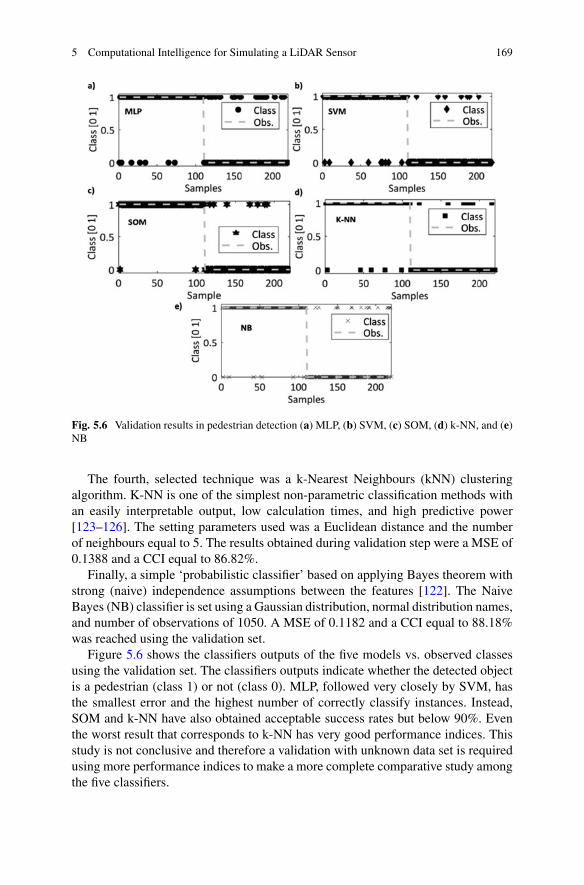
5 Computational Intelligence for Simulating a LiDAR Sensor 169
Fig. 5.6 Validation results in pedestrian detection (a) MLP, (b) SVM, (c) SOM, (d) k-NN, and (e)NB
The fourth, selected technique was a k-Nearest Neighbours (kNN) clusteringalgorithm. K-NN is one of the simplest non-parametric classification methods withan easily interpretable output, low calculation times, and high predictive power[123–126]. The setting parameters used was a Euclidean distance and the numberof neighbours equal to 5. The results obtained during validation step were a MSE of0.1388 and a CCI equal to 86.82%.
Finally, a simple ‘probabilistic classifier’ based on applying Bayes theorem withstrong (naive) independence assumptions between the features [122]. The NaiveBayes (NB) classifier is set using a Gaussian distribution, normal distribution names,and number of observations of 1050. A MSE of 0.1182 and a CCI equal to 88.18%was reached using the validation set.
Figure 5.6 shows the classifiers outputs of the five models vs. observed classesusing the validation set. The classifiers outputs indicate whether the detected objectis a pedestrian (class 1) or not (class 0). MLP, followed very closely by SVM, hasthe smallest error and the highest number of correctly classify instances. Instead,SOM and k-NN have also obtained acceptable success rates but below 90%. Eventhe worst result that corresponds to k-NN has very good performance indices. Thisstudy is not conclusive and therefore a validation with unknown data set is requiredusing more performance indices to make a more complete comparative study amongthe five classifiers.
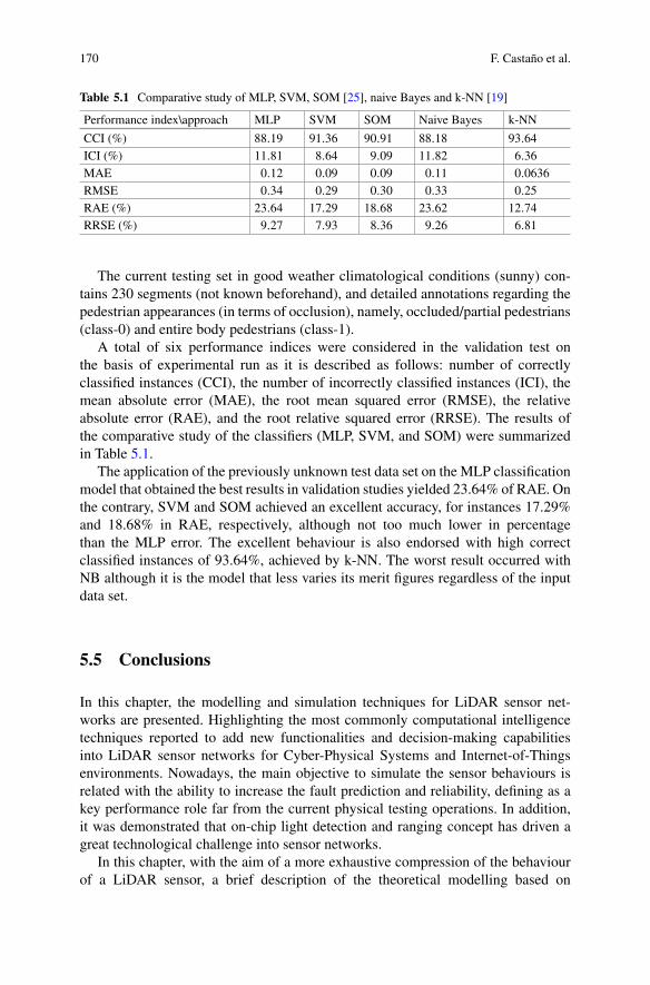
170 F. Castaño et al.
Table 5.1 Comparative study of MLP, SVM, SOM [25], naive Bayes and k-NN [19]
Performance index\approach MLP SVM SOM Naive Bayes k-NN
CCI (%) 88.19 91.36 90.91 88.18 93.64ICI (%) 11.81 8.64 9.09 11.82 6.36MAE 0.12 0.09 0.09 0.11 0.0636RMSE 0.34 0.29 0.30 0.33 0.25RAE (%) 23.64 17.29 18.68 23.62 12.74RRSE (%) 9.27 7.93 8.36 9.26 6.81
The current testing set in good weather climatological conditions (sunny) con-tains 230 segments (not known beforehand), and detailed annotations regarding thepedestrian appearances (in terms of occlusion), namely, occluded/partial pedestrians(class-0) and entire body pedestrians (class-1).
A total of six performance indices were considered in the validation test onthe basis of experimental run as it is described as follows: number of correctlyclassified instances (CCI), the number of incorrectly classified instances (ICI), themean absolute error (MAE), the root mean squared error (RMSE), the relativeabsolute error (RAE), and the root relative squared error (RRSE). The results ofthe comparative study of the classifiers (MLP, SVM, and SOM) were summarizedin Table 5.1.
The application of the previously unknown test data set on the MLP classificationmodel that obtained the best results in validation studies yielded 23.64% of RAE. Onthe contrary, SVM and SOM achieved an excellent accuracy, for instances 17.29%and 18.68% in RAE, respectively, although not too much lower in percentagethan the MLP error. The excellent behaviour is also endorsed with high correctclassified instances of 93.64%, achieved by k-NN. The worst result occurred withNB although it is the model that less varies its merit figures regardless of the inputdata set.
5.5 Conclusions
In this chapter, the modelling and simulation techniques for LiDAR sensor net-works are presented. Highlighting the most commonly computational intelligencetechniques reported to add new functionalities and decision-making capabilitiesinto LiDAR sensor networks for Cyber-Physical Systems and Internet-of-Thingsenvironments. Nowadays, the main objective to simulate the sensor behaviours isrelated with the ability to increase the fault prediction and reliability, defining as akey performance role far from the current physical testing operations. In addition,it was demonstrated that on-chip light detection and ranging concept has driven agreat technological challenge into sensor networks.
In this chapter, with the aim of a more exhaustive compression of the behaviourof a LiDAR sensor, a brief description of the theoretical modelling based on
5 Computational Intelligence for Simulating a LiDAR Sensor 171
mathematical principles of operation is outlined. The mathematical modelling isfocused on the radiometric aspect of single LiDAR that is composed by differentsubmodules, such as laser beam, returned energy, and energy noise. As an example,this sensor model is implemented, assuming the most simplified use case which is asingle laser and a single array of photodetectors without scanning and will be usedin the later simulation steps.
Subsequently, the chapter describes a general overview of state-of-the-art com-putational intelligence techniques commonly used in sensor system simulationapplications. Some of these applications are AI-based techniques for CPS and IoTsensor network solutions, computational intelligence for pattern recognition andvision classification sensor-based analytics, localization optimization, and energyconsumption in WSN. In summary, the technical review draws the following keyconcluding remarks. Firstly, due the great advance of informatics and communi-cation technologies, which has allowed the rebirth of the AI-based solutions, theapplications of machine-learning algorithms in engineering have risen especiallyin fields of recent emergence such as CPS, and IoT. Furthermore, the WSN,considered one particular field into the IoT-based solutions, has also received a lotof attention on the application of ML algorithms, becoming one of the main tools toaddress the main challenges for implementation in industrial and services scenarios.Secondly, the near future will demand fast solution in unknown situations, becomingboth the sensor and computational intelligence fusion key issues to develop morerobust, efficient, and safety human–machine ecosystems. Finally, the computationalintelligence-based solutions have become relevant to optimize localization, energy,and accuracy in current and future sensor networks, improving higher levels ofefficiency, reliability, and self-healing capacities.
In order to corroborate the potential of the computational intelligence for addingnew capabilities to sensor networks in Cyber-Physical Systems and Internet-of-Things environments, a use case is presented. CI methods were applied to a 3Dscenario simulation software (Webots) for automobiles, using the mathematicalLiDAR model defined in this chapter. The application of a model library forobject classification tasks, using the LiDAR data in a virtual sensor networkfor obstacle recognition actions in driving assistance in a Cyber-Physical Systemscenario showed very promising results. Four artificial intelligence-based methodsand a probabilistic method for obstacle recognition were applied: a multi-layerperceptron, a self-organized map, a support vector machine, k-nearest neighboursand naive Bayesian network. The results demonstrated the suitability of applyingcomputational intelligence methods to increase the reliability of sensor networks,addressing the key challenges to increase the safety and security in automotiveapplications.
Acknowledgments The authors wish to thank the support given by the European projectIoSENSE: Flexible FE/BE Sensor Pilot Line for the Internet of Everything. This project hasreceived funding from the Electronic Component Systems for European Leadership Joint Under-taking under grant agreement No 692480. This Joint Undertaking receives support from theEuropean Union’s Horizon 2020 research and innovation programme and Germany, Saxony,Austria, Belgium, the Netherlands, Slovakia, and Spain.
172 F. Castaño et al.
References
1. A.J.C. Trappey, C.V. Trappey, U.H. Govindarajan, J.J. Sun, A.C. Chuang,A review of technology standards and patent portfolios for enabling cyber-physical systems in advanced manufacturing. IEEE Access 4, 7356–7382 (2016).https://doi.org/10.1109/ACCESS.2016.2619360
2. X. Krasniqi, E. Hajrizi, Use of IoT technology to drive the automotive industry fromconnected to full autonomous vehicles. IFAC-PapersOnLine 49(29), 269–274 (2016).https://doi.org/10.1016/j.ifacol.2016.11.078
3. J. Pajares Redondo, L. Prieto González, J. García Guzman, B.L. Boada, V. Díaz, VEHIOT:Design and evaluation of an IoT architecture based on low-cost devices to be embedded inproduction vehicles. Sensors 18(2), 486 (2018)
4. T. Bures, D. Weyns, M. Klein, R.E. Haber, 1st International Workshop on SoftwareEngineering for Smart Cyber-Physical Systems (SEsCPS 2015), in 2015 IEEE/ACM 37thIEEE International Conference on Software Engineering, 16-24 May 2015, (2015), pp. 1009–1010. https://doi.org/10.1109/ICSE.2015.326
5. J. Lee, B. Bagheri, H.-A. Kao, A cyber-physical systems architecture for industry 4.0-basedmanufacturing systems. Manufact. Lett. 3, 18–23 (2015b)
6. T. Sanislav, L. Miclea, Cyber-physical systems-concept, challenges and research areas. J.Contr. Eng. Appl. Inform. 14(2), 28–33 (2012)
7. A. Bhave, B.H. Krogh, D. Garlan, B. Schmerl, View consistency in architectures for cyber-physical systems, in Proceedings of the 2011 IEEE/ACM Second International Conference onCyber-Physical Systems, (IEEE Computer Society, 2011), pp. 151–160
8. P. Gölzer, P. Cato, M. Amberg, Data Processing Requirements of Industry 4.0-Use Cases forBig Data Applications, in ECIS, (2015)
9. X. Yuan, C.J. Anumba, K.M. Parfitt, Review of the potential for a cyber-physical systemapproach to temporary structures monitoring. Int. J. Architect. Res. ArchNet-IJAR 9(3), 26–44 (2015)
10. T. Watteyne, V. Handziski, X. Vilajosana, S. Duquennoy, O. Hahm, E. Baccelli, A. Wolisz,Industrial wireless ip-based cyber–physical systems. Proc. IEEE 104(5), 1025–1038 (2016)
11. J. Wan, D. Zhang, S. Zhao, L. Yang, J. Lloret, Context-aware vehicular cyber-physicalsystems with cloud support: architecture, challenges, and solutions. IEEE Commun. Mag.52(8), 106–113 (2014)
12. J. Ruan, W. Yu, Y. Yang, J. Hu, Design and realize of tire production process monitoringsystem based on cyber-physical systems, in 2015 International Conference on ComputerScience and Mechanical Automation (CSMA), (IEEE, 2015), pp. 175–179
13. A. Iovine, F. Valentini, E. De Santis, M.D. Di Benedetto, M. Pratesi, Safe human-inspiredmesoscopic hybrid automaton for autonomous vehicles. Nonlinear Anal. Hybrid Syst. 25,192–210 (2017). https://doi.org/10.1016/j.nahs.2016.08.008
14. D. Reiser, D. Paraforos, M. Khan, H. Griepentrog, M. Vázquez-Arellano, Autonomous fieldnavigation, data acquisition and node location in wireless sensor networks. Precis. Agric.,1–14 (2016)
15. X. Zhao, K. Mu, F. Hui, C. Prehofer, A cooperative vehicle-infrastructure based urban drivingenvironment perception method using a D-S theory-based credibility map. Optik 138, 407–415 (2017). https://doi.org/10.1016/j.ijleo.2017.03.102
16. W. Rapberger, The emergence of autonomous vehicles. Accenture (2017)17. C.-I. Chen, R. Koseluk, C. Buchanan, A. Duerner, B. Jeppesen, H. Laux, Autonomous aerial
refueling ground test demonstration—A sensor-in-the-loop, non-tracking method. Sensors15(5), 10948–10972 (2015)
18. G. Pandey, J.R. McBride, S. Savarese, R.M. Eustice, Automatic extrinsic calibration of visionand lidar by maximizing mutual information. J. Field Robot. 32(5), 696–722 (2015)
19. S. Sim, J. Sock, K. Kwak, Indirect correspondence-based robust extrinsic calibration ofLiDAR and camera. Sensors 16(6), 933 (2016)
5 Computational Intelligence for Simulating a LiDAR Sensor 173
20. R. Vivacqua, R. Vassallo, F. Martins, A low cost sensors approach for accurate vehiclelocalization and autonomous driving application. Sensors 17(10), 2359 (2017)
21. M. Ahmad, Reliability models for the internet of things: a paradigm shift, in Paper Presentedat the 2014 IEEE International Symposium on Software Reliability Engineering Workshops,3-6 Nov 2014, (2014)
22. L. Xiao, R. Wang, B. Dai, Y. Fang, D. Liu, T. Wu, Hybrid conditional random fieldbased camera-LIDAR fusion for road detection. Inform. Sci. 432, 543–558 (2018b).https://doi.org/10.1016/j.ins.2017.04.048
23. Y. Zeng, H. Yu, H. Dai, S. Song, M. Lin, B. Sun, W. Jiang, M. Meng, An Improved CalibrationMethod for a Rotating 2D LIDAR System. Sensors 18(2), 497 (2018)
24. S. Hu, Z. Li, Z. Zhang, D. He, M. Wimmer, Efficient tree modeling from airborne LiDARpoint clouds. Comput. Graph. 67, 1–13 (2017). https://doi.org/10.1016/j.cag.2017.04.004
25. F. Castaño, G. Beruvides, R. Haber, A. Artuñedo, Obstacle recognition based on machinelearning for On-Chip LiDAR sensors in a cyber-physical system. Sensors 17(9), 2109 (2017a)
26. R. Kala, 3—Perception in autonomous vehicles, in On-road intel-ligent vehicles, (Butterworth-Heinemann, Oxford, 2016), pp. 36–58.https://doi.org/10.1016/B978-0-12-803729-4.00003-9
27. A. Apatean, A. Rogozan, A. Bensrhair, Visible-infrared fusion schemes for roadobstacle classification. Transport. Res. Pt. C Emerg. Technol. 35, 180–192 (2013).https://doi.org/10.1016/j.trc.2013.07.003
28. H. Taghavifar, A. Mardani, H. Karim Maslak, A comparative study between arti-ficial neural networks and support vector regression for modeling of the dissi-pated energy through tire-obstacle collision dynamics. Energy 89, 358–364 (2015).https://doi.org/10.1016/j.energy.2015.05.122
29. P.J. Navarro, C. Fernández, R. Borraz, D. Alonso, A machine learning approach to pedestriandetection for autonomous vehicles using high-definition 3D range data. Sensors 17(1), 18(2016)
30. B. Shi, L. Han, H. Yan, Adaptive clustering algorithm based on kNN and density. PatternRecogn. Lett. 104, 37–44 (2018). https://doi.org/10.1016/j.patrec.2018.01.020
31. S. Zhang, D. Cheng, Z. Deng, M. Zong, X. Deng, A novel kNN algorithmwith data-driven k parameter computation. Pattern Recogn. Lett. (2017).https://doi.org/10.1016/j.patrec.2017.09.036
32. D. Bein, V. Jolly, B. Kumar, S. Latifi, Reliability modeling in wireless sensor networks. Int.J. Inform. Technol. 11(2), 1–8 (2005)
33. H.M.F. AboElFotoh, S.S. Iyengar, K. Chakrabarty, Computing reliability and message delayfor Cooperative wireless distributed sensor networks subject to random failures. IEEE Trans.Reliabil. 54(1), 145–155 (2005). https://doi.org/10.1109/TR.2004.842540
34. A. Artuñedo, J. Godoy, R. Haber, J. Villagrá, Toro RMd Advanced Co-simulation Frameworkfor Cooperative Maneuvers Among Vehicles, in 2015 IEEE 18th International Confer-ence on Intelligent Transportation Systems, 15-18 Sept. 2015, (2015), pp. 1436–1441.https://doi.org/10.1109/ITSC.2015.235
35. Z. Zhang, E. Eyisi, X. Koutsoukos, J. Porter, G. Karsai, J. Sztipanovits, A co-simulationframework for design of time-triggered automotive cyber physical systems. Simul. Model.Pract. Theor. 43, 16–33 (2014). https://doi.org/10.1016/j.simpat.2014.01.001
36. F. Ferracuti, A. Freddi, A. Monteriù, M. Prist, An integrated simulation module for cyber-physical automation systems. Sensors 16(5), 645 (2016)
37. I.D. de Souza, S.N. Silva, R.M. Teles, M.A. Fernandes, Platform for real-time simulation ofdynamic systems and hardware-in-the-loop for control algorithms. Sensors 14(10), 19176–19199 (2014)
38. M. Mozumdar, Z.Y. Song, L. Lavagno, A.L. Sangiovanni-Vincentelli, A model-basedapproach for bridging virtual and physical sensor nodes in a hybrid simulation framework.Sensors 14(6), 11070–11096 (2014)
39. B.-H. Lee, J.-H. Song, J.-H. Im, S.-H. Im, M.-B. Heo, G.-I. Jee, GPS/DR error estimation forautonomous vehicle localization. Sensors 15(8), 20779–20798 (2015a)
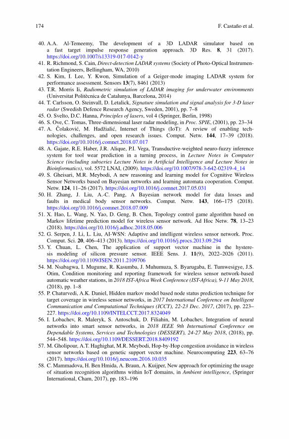
174 F. Castaño et al.
40. A.A. Al-Temeemy, The development of a 3D LADAR simulator based ona fast target impulse response generation approach. 3D Res. 8, 31 (2017).https://doi.org/10.1007/s13319-017-0142-y
41. R. Richmond, S. Cain, Direct-detection LADAR systems (Society of Photo-Optical Instrumen-tation Engineers, Bellingham, WA, 2010)
42. S. Kim, I. Lee, Y. Kwon, Simulation of a Geiger-mode imaging LADAR system forperformance assessment. Sensors 13(7), 8461 (2013)
43. T.R. Morris Ii, Radiometric simulation of LADAR imaging for underwater environments(Universitat Politècnica de Catalunya, Barcelona, 2014)
44. T. Carlsson, O. Steinvall, D. Letalick, Signature simulation and signal analysis for 3-D laserradar (Swedish Defence Research Agency, Sweden, 2001), pp. 7–8
45. O. Svelto, D.C. Hanna, Principles of lasers, vol 4 (Springer, Berlin, 1998)46. S. Ove, C. Tomas, Three-dimensional laser radar modeling, in Proc. SPIE, (2001), pp. 23–3447. A. Colakovic, M. Hadžialic, Internet of Things (IoT): A review of enabling tech-
nologies, challenges, and open research issues. Comput. Netw. 144, 17–39 (2018).https://doi.org/10.1016/j.comnet.2018.07.017
48. A. Gajate, R.E. Haber, J.R. Alique, P.I. Vega, Transductive-weighted neuro-fuzzy inferencesystem for tool wear prediction in a turning process, in Lecture Notes in ComputerScience (including subseries Lecture Notes in Artificial Intelligence and Lecture Notes inBioinformatics), vol. 5572 LNAI, (2009). https://doi.org/10.1007/978-3-642-02319-4_14
49. S. Gheisari, M.R. Meybodi, A new reasoning and learning model for Cognitive WirelessSensor Networks based on Bayesian networks and learning automata cooperation. Comput.Netw. 124, 11–26 (2017). https://doi.org/10.1016/j.comnet.2017.05.031
50. H. Zhang, J. Liu, A.-C. Pang, A Bayesian network model for data losses andfaults in medical body sensor networks. Comput. Netw. 143, 166–175 (2018).https://doi.org/10.1016/j.comnet.2018.07.009
51. X. Hao, L. Wang, N. Yao, D. Geng, B. Chen, Topology control game algorithm based onMarkov lifetime prediction model for wireless sensor network. Ad Hoc Netw. 78, 13–23(2018). https://doi.org/10.1016/j.adhoc.2018.05.006
52. G. Serpen, J. Li, L. Liu, AI-WSN: Adaptive and intelligent wireless sensor network. Proc.Comput. Sci. 20, 406–413 (2013). https://doi.org/10.1016/j.procs.2013.09.294
53. Y. Chuan, L. Chen, The application of support vector machine in the hystere-sis modeling of silicon pressure sensor. IEEE Sens. J. 11(9), 2022–2026 (2011).https://doi.org/10.1109/JSEN.2011.2109706
54. M. Nsabagwa, I. Mugume, R. Kasumba, J. Muhumuza, S. Byarugaba, E. Tumwesigye, J.S.Otim, Condition monitoring and reporting framework for wireless sensor network-basedautomatic weather stations, in 2018 IST-Africa Week Conference (IST-Africa), 9-11 May 2018,(2018), pp. 1–8
55. P. Chaturvedi, A.K. Daniel, Hidden markov model based node status prediction technique fortarget coverage in wireless sensor networks, in 2017 International Conference on IntelligentCommunication and Computational Techniques (ICCT), 22-23 Dec. 2017, (2017), pp. 223–227. https://doi.org/10.1109/INTELCCT.2017.8324049
56. I. Lobachev, R. Maleryk, S. Antoschuk, D. Filiahin, M. Lobachev, Integration of neuralnetworks into smart sensor networks, in 2018 IEEE 9th International Conference onDependable Systems, Services and Technologies (DESSERT), 24-27 May 2018, (2018), pp.544–548. https://doi.org/10.1109/DESSERT.2018.8409192
57. M. Gholipour, A.T. Haghighat, M.R. Meybodi, Hop-by-Hop congestion avoidance in wirelesssensor networks based on genetic support vector machine. Neurocomputing 223, 63–76(2017). https://doi.org/10.1016/j.neucom.2016.10.035
58. C. Mammadova, H. Ben Hmida, A. Braun, A. Kuijper, New approach for optimizing the usageof situation recognition algorithms within IoT domains, in Ambient intelligence, (SpringerInternational, Cham, 2017), pp. 183–196
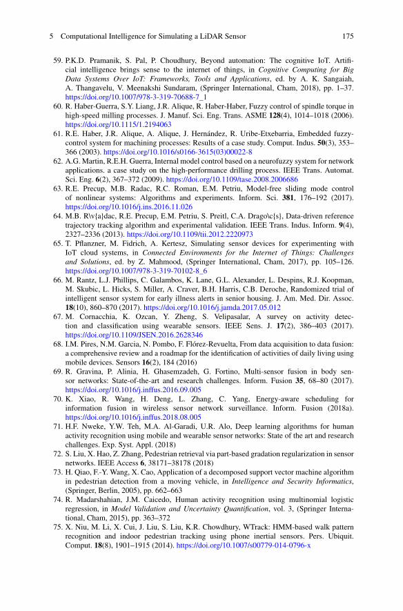
5 Computational Intelligence for Simulating a LiDAR Sensor 175
59. P.K.D. Pramanik, S. Pal, P. Choudhury, Beyond automation: The cognitive IoT. Artifi-cial intelligence brings sense to the internet of things, in Cognitive Computing for BigData Systems Over IoT: Frameworks, Tools and Applications, ed. by A. K. Sangaiah,A. Thangavelu, V. Meenakshi Sundaram, (Springer International, Cham, 2018), pp. 1–37.https://doi.org/10.1007/978-3-319-70688-7_1
60. R. Haber-Guerra, S.Y. Liang, J.R. Alique, R. Haber-Haber, Fuzzy control of spindle torque inhigh-speed milling processes. J. Manuf. Sci. Eng. Trans. ASME 128(4), 1014–1018 (2006).https://doi.org/10.1115/1.2194063
61. R.E. Haber, J.R. Alique, A. Alique, J. Hernández, R. Uribe-Etxebarria, Embedded fuzzy-control system for machining processes: Results of a case study. Comput. Indus. 50(3), 353–366 (2003). https://doi.org/10.1016/s0166-3615(03)00022-8
62. A.G. Martin, R.E.H. Guerra, Internal model control based on a neurofuzzy system for networkapplications. a case study on the high-performance drilling process. IEEE Trans. Automat.Sci. Eng. 6(2), 367–372 (2009). https://doi.org/10.1109/tase.2008.2006686
63. R.E. Precup, M.B. Radac, R.C. Roman, E.M. Petriu, Model-free sliding mode controlof nonlinear systems: Algorithms and experiments. Inform. Sci. 381, 176–192 (2017).https://doi.org/10.1016/j.ins.2016.11.026
64. M.B. R\v{a}dac, R.E. Precup, E.M. Petriu, S. Preitl, C.A. Drago\c{s}, Data-driven referencetrajectory tracking algorithm and experimental validation. IEEE Trans. Indus. Inform. 9(4),2327–2336 (2013). https://doi.org/10.1109/tii.2012.2220973
65. T. Pflanzner, M. Fidrich, A. Kertesz, Simulating sensor devices for experimenting withIoT cloud systems, in Connected Environments for the Internet of Things: Challengesand Solutions, ed. by Z. Mahmood, (Springer International, Cham, 2017), pp. 105–126.https://doi.org/10.1007/978-3-319-70102-8_6
66. M. Rantz, L.J. Phillips, C. Galambos, K. Lane, G.L. Alexander, L. Despins, R.J. Koopman,M. Skubic, L. Hicks, S. Miller, A. Craver, B.H. Harris, C.B. Deroche, Randomized trial ofintelligent sensor system for early illness alerts in senior housing. J. Am. Med. Dir. Assoc.18(10), 860–870 (2017). https://doi.org/10.1016/j.jamda.2017.05.012
67. M. Cornacchia, K. Ozcan, Y. Zheng, S. Velipasalar, A survey on activity detec-tion and classification using wearable sensors. IEEE Sens. J. 17(2), 386–403 (2017).https://doi.org/10.1109/JSEN.2016.2628346
68. I.M. Pires, N.M. Garcia, N. Pombo, F. Flórez-Revuelta, From data acquisition to data fusion:a comprehensive review and a roadmap for the identification of activities of daily living usingmobile devices. Sensors 16(2), 184 (2016)
69. R. Gravina, P. Alinia, H. Ghasemzadeh, G. Fortino, Multi-sensor fusion in body sen-sor networks: State-of-the-art and research challenges. Inform. Fusion 35, 68–80 (2017).https://doi.org/10.1016/j.inffus.2016.09.005
70. K. Xiao, R. Wang, H. Deng, L. Zhang, C. Yang, Energy-aware scheduling forinformation fusion in wireless sensor network surveillance. Inform. Fusion (2018a).https://doi.org/10.1016/j.inffus.2018.08.005
71. H.F. Nweke, Y.W. Teh, M.A. Al-Garadi, U.R. Alo, Deep learning algorithms for humanactivity recognition using mobile and wearable sensor networks: State of the art and researchchallenges. Exp. Syst. Appl. (2018)
72. S. Liu, X. Hao, Z. Zhang, Pedestrian retrieval via part-based gradation regularization in sensornetworks. IEEE Access 6, 38171–38178 (2018)
73. H. Qiao, F.-Y. Wang, X. Cao, Application of a decomposed support vector machine algorithmin pedestrian detection from a moving vehicle, in Intelligence and Security Informatics,(Springer, Berlin, 2005), pp. 662–663
74. R. Madarshahian, J.M. Caicedo, Human activity recognition using multinomial logisticregression, in Model Validation and Uncertainty Quantification, vol. 3, (Springer Interna-tional, Cham, 2015), pp. 363–372
75. X. Niu, M. Li, X. Cui, J. Liu, S. Liu, K.R. Chowdhury, WTrack: HMM-based walk patternrecognition and indoor pedestrian tracking using phone inertial sensors. Pers. Ubiquit.Comput. 18(8), 1901–1915 (2014). https://doi.org/10.1007/s00779-014-0796-x
176 F. Castaño et al.
76. Z. Yang, L.S.C. Pun-Cheng, Vehicle detection in intelligent transportation systems and itsapplications under varying environments: A review. Image Vision Comput. 69, 143–154(2018). https://doi.org/10.1016/j.imavis.2017.09.008
77. W. Shi, M.B. Alawieh, X. Li, H. Yu, Algorithm and hardware implementation for visualperception system in autonomous vehicle: A survey. Integration 59, 148–156 (2017).https://doi.org/10.1016/j.vlsi.2017.07.007
78. F. Li, Z. Lv, Reliable vehicle type recognition based on information fusion in multiple sensornetworks. Comput. Netw. 117, 76–84 (2017)
79. M.B.B. Mahaleh, S.A. Mirroshandel, Harmony search path detection for visionbased automated guided vehicle. Robot. Auton. Syst. 107, 156–166 (2018).https://doi.org/10.1016/j.robot.2018.06.008
80. G. Beruvides, R. Quiza, R. Del Toro, R.E. Haber, Sensoring systems and signal analysis tomonitor tool wear in microdrilling operations on a sintered tungsten-copper composite mate-rial. Sens. Actuat. A. Phys. 199, 165–175 (2013). https://doi.org/10.1016/j.sna.2013.05.021
81. I. Kabashkin, J. Kundler, Reliability of sensor nodes in wireless sensor networks of cyberphysical systems. Proc. Comput. Sci. 104, 380–384 (2017)
82. L.A. Laranjeira, G.N. Rodrigues, Border effect analysis for reliability assurance and continu-ous connectivity of wireless sensor networks in the presence of sensor failures. IEEE Trans.Wirel. Commun. 13(8), 4232–4246 (2014)
83. M. Yan, K.-Y. Lam, S. Han, E. Chan, Q. Chen, P. Fan, D. Chen, M. Nixon, Hypergraph-baseddata link layer scheduling for reliable packet delivery in wireless sensing and control networkswith end-to-end delay constraints. Inform. Sci. 278, 34–55 (2014)
84. M.-T. Vo, T.T. Thanh Nghi, V.-S. Tran, L. Mai, C.-T. Le, Wireless sensor network for realtime healthcare monitoring: Network design and performance evaluation simulation, in 5thInternational Conference on Biomedical Engineering in Vietnam, (Springer International,Cham, 2015), pp. 87–91
85. D. Cacciagrano, R. Culmone, M. Micheletti, L. Mostarda, Energy-efficient clustering forwireless sensor devices in internet of things, in Performability in Internet of Things, (Springer,Cham, 2019), pp. 59–80
86. S. Hossain, A.R. Fayjie, O. Doukhi, D.-J. Lee, CAIAS Simulator: Self-driving Vehicle Simu-lator for AI Research, in International Conference on Intelligent Computing & Optimization,(Springer, Berlin, 2018), pp. 187–195
87. M. Mukherjee, I. Adhikary, S. Mondal, A.K. Mondal, M. Pundir, V.A. Chowdary, Vision ofIoT: Applications, Challenges, and Opportunities with Dehradun Perspective, in Proceedingof International Conference on Intelligent Communication, Control and Devices, (Springer,Singapore, 2017), pp. 553–559
88. A. Bradai, A. Benslimane, K.D. Singh, Dynamic anchor points selection for mobilitymanagement in software defined networks. J. Netw. Comput. Appl. 57, 1–11 (2015)
89. S. Kumar, D. Lobiyal, Novel DV-Hop localization algorithm for wireless sensor networks.Telecommun. Syst. 64(3), 509–524 (2017)
90. J. Hightower, G. Borriello, Location systems for ubiquitous computing. Computer 34(8), 57–66 (2001). https://doi.org/10.1109/2.940014
91. G.J. Pottie, W.J. Kaiser, Wireless integrated network sensors. Commun. ACM 43(5), 51–58(2000). https://doi.org/10.1145/332833.332838
92. N.B. Priyantha, A. Chakraborty, H. Balakrishnan, The Cricket location-support system, inPaper presented at the Proceedings of the 6th annual international conference on Mobilecomputing and networking, Boston, Massachusetts, USA, (2000)
93. A. Savvides, C.-C. Han, M.B. Strivastava, Dynamic fine-grained localization in Ad-Hocnetworks of sensors, in Paper presented at the Proceedings of the 7th annual internationalconference on Mobile computing and networking, Rome, Italy, (2001)
94. J. Sheu, P. Chen, C. Hsu, A distributed localization scheme for wireless sensor networks withimproved grid-scan and vector-based refinement. IEEE Trans. Mob. Comput. 7(9), 1110–1123(2008). https://doi.org/10.1109/TMC.2008.35
5 Computational Intelligence for Simulating a LiDAR Sensor 177
95. T. He, C. Huang, B.M. Blum, J.A. Stankovic, T. Abdelzaher, Range-free localization schemesfor large scale sensor networks, in Paper presented at the Proceedings of the 9th annualinternational conference on Mobile computing and networking, San Diego, CA, USA, (2003)
96. F. Tlili, A. Rachedi, A. Benslimane, Time-bounded localization algorithm based ondistributed multidimensional scaling for wireless sensor networks, in 2014 IEEE Inter-national Conference on Communications (ICC), 10-14 June 2014, (2014), pp. 233–238.https://doi.org/10.1109/ICC.2014.6883324
97. A. Khan, I. Ali, H.A. Mahmood, Localization free variable transmit power routing protocolfor underwater wireless sensor networks, in Advances in Network-Based Information Systems,(Springer International, Cham, 2018), pp. 136–147
98. L. Cui, C. Xu, G. Li, Z. Ming, Y. Feng, N. Lu, A high accurate localization algorithm withDV-Hop and differential evolution for wireless sensor network. Appl. Soft Comput. 68, 39–52(2018)
99. S.K. Gharghan, R. Nordin, A.M. Jawad, H.M. Jawad, M. Ismail, Adaptive neural fuzzyinference system for accurate localization of wireless sensor network in outdoor and indoorcycling applications. IEEE Access 6, 38475–38489 (2018)
100. G. Beruvides, R. Quiza, R.E. Haber, Multi-objective optimization based on an improvedcross-entropy method. A case study of a micro-scale manufacturing process. Inform. Sci.334-335, 161–173 (2016). https://doi.org/10.1016/j.ins.2015.11.040
101. R.E. Haber, G. Beruvides, R. Quiza, A. Hernandez, A simple multi-objective opti-mization based on the cross-entropy method. IEEE Access 5, 22272–22281 (2017).https://doi.org/10.1109/access.2017.2764047
102. A.J. Perez, M-SPOT: A hybrid multiobjective evolutionary algorithm for node placement inwireless sensor networks, in 2018 32nd International Conference on Advanced InformationNetworking and Applications Workshops (WAINA), 16-18 May 2018, (2018), pp. 264–269.https://doi.org/10.1109/WAINA.2018.00096
103. S. Phoemphon, C. So-In, D.T. Niyato, A hybrid model using fuzzy logic and an extremelearning machine with vector particle swarm optimization for wireless sensor networklocalization. Appl. Soft Comput. 65, 101–120 (2018)
104. Y. Xu, L. Wang, Z. Wang, Y. Lv, Y. Zhang, W. Chen, Using differential evolution to researchthe multi-objective optimization of medical sensor networks: A brief discussion, in 2018Chinese Control And Decision Conference (CCDC), (IEEE, 2018)
105. K. Singh, K. Singh, A. Aziz, Congestion control in wireless sensor networks by hybrid multi-objective optimization algorithm. Comput. Netw. 138, 90–107 (2018)
106. S. Amri, F. Khelifi, A. Bradai, A. Rachedi, M.L. Kaddachi, M. Atri, A new fuzzy logic basednode localization mechanism for wireless sensor networks. Future Gener. Comput. Syst. 93,799–813 (2017)
107. N.A. Pantazis, S.A. Nikolidakis, D.D. Vergados, Energy-efficient routing protocols inwireless sensor networks: A survey. IEEE Commun. Surv. Tutor. 15(2), 551–591 (2013).https://doi.org/10.1109/SURV.2012.062612.00084
108. N. Ramluckun, V. Bassoo, Energy-efficient chain-cluster based intelligent routing techniquefor wireless sensor networks. Appl. Comput. Inform. (2018)
109. R. Logambigai, S. Ganapathy, A. Kannan, Energy–efficient grid–based routing algorithmusing intelligent fuzzy rules for wireless sensor networks. Comput. Electr. Eng. 68, 62–75(2018)
110. S.B. Shah, Z. Chen, F. Yin, I.U. Khan, N. Ahmad, Energy and interoperable aware routing forthroughput optimization in clustered IoT-wireless sensor networks. Future Gener. Comput.Syst. 81, 372–381 (2018)
111. S. Su, S. Zhao, An optimal clustering mechanism based on Fuzzy-C means for wireless sensornetworks. Sustain. Comput. Inform. Syst. 18, 127–134 (2018)
112. W. Elsayed, M. Elhoseny, S. Sabbeh, A. Riad, Self-maintenance model for wireless sensornetworks. Comput. Electr. Eng. 70, 799–812 (2017)

178 F. Castaño et al.
113. H. He, Z. Zhu, E. Makinen, A neural network model to minimize the connected dominatingset for self-configuration of wireless sensor networks. IEEE Trans. Neural Netw. 20(6), 973–982 (2009)
114. F. Castaño, G. Beruvides, R.E. Haber, A. Villalonga, Time-To-failure modelling in On-ChipLiDAR sensors for automotive applications. Proceedings 1(8), 809 (2017b)
115. F. Castaño, G. Beruvides, A. Villalonga, R.E. Haber, Self-tuning method for increasedobstacle detection reliability based on internet of things LiDAR sensor models. Sensors(Switzerland) 18(5) (2018). https://doi.org/10.3390/s18051508
116. O. Michel, Cyberbotics Ltd. Webots™: professional mobile robot simulation. Int. J. Adv.Robot. Syst. 1(1), 5 (2004)
117. J. Godoy, J. Pérez, E. Onieva, J. Villagrá, V. Milanés, R. Haber, A driverless vehicledemonstration on motorways and in urban environments. Transport 30(3), 253–263 (2015).https://doi.org/10.3846/16484142.2014.1003406
118. A. Alique, R.E. Haber, R.H. Haber, S. Ros, C. Gonzalez, Neural network-based model forthe prediction of cutting force in milling process. A progress study on a real case, in IEEEInternational Symposium on Intelligent Control—Proceedings, (2000), pp. 121–125
119. I.L. Fe, G. Beruvides, R. Quiza, R. Haber, M. Rivas, Automatic selection of optimal parame-ters based on simple soft computing methods. A case study on micro-milling processes. IEEETrans. Indus. Inform. 99, 1-1 (2018). https://doi.org/10.1109/TII.2018.2816971
120. R.E. Haber, J.R. Alique, Nonlinear internal model control using neural networks:An application for machining processes. Neural Comput. Appl. 13(1), 47–55 (2004).https://doi.org/10.1007/s00521-003-0394-8
121. E.M. Voumvoulakis, N.D. Hatziargyriou, Decision trees-aided self-organized maps forcorrective dynamic security. IEEE Trans. Power Syst. 23(2), 622–630 (2008)
122. M.N. Murty, R. Raghava, Kernel-based SVM, in Support Vector Machines and Perceptrons:Learning, Optimization, Classification, and Application to Social Networks, (Springer Inter-national, Cham, 2016), pp. 57–67. https://doi.org/10.1007/978-3-319-41063-0_5
123. S. Aziz, E.A. Mohamed, F. Youssef, Traffic sign recognition based on multi-feature fusion and ELM classifier. Proc. Comput. Sci. 127, 146–153 (2018).https://doi.org/10.1016/j.procs.2018.01.109
124. G. Beruvides, F. Castaño, R.E. Haber, R. Quiza, A. Villalonga, Coping with complexity whenpredicting surface roughness in milling processes: Hybrid incremental model with optimalparametrization. Complexity (2017). https://doi.org/10.1155/2017/7317254
125. B. Khaldi, F. Harrou, F. Cherif, Y. Sun, Self-organization in aggregating robotswarms: A DW-KNN topological approach. Biosystems 165, 106–121 (2018).https://doi.org/10.1016/j.biosystems.2018.01.005
126. F. Penedo, R.E. Haber, A. Gajate, R.M. Del Toro, Hybrid incremental modeling based on leastsquares and fuzzy K-NN for monitoring tool wear in turning processes. IEEE Trans. Indus.Inform. 8(4), 811–818 (2012). https://doi.org/10.1109/TII.2012.2205699
Chapter 6A Smartphone-Based Virtual White CanePrototype Featuring Time-of-Flight 3DImaging
Norbert Druml, Thomas Pietsch, Marcus Baumgart, Cristina Consani,Thomas Herndl, and Gerald Holweg
6.1 Introduction
In 2014, the World Health Organization (WHO) estimated that there were 285 mil-lion visually impaired people worldwide, with 246 million having low vision and39 million being blind. It is a challenging task for the visually impaired to safely andquickly navigate through an unknown or unfamiliar environment. Still the traditionalwhite cane and the guide dog are the most common and reliable travel aids available.However, using the traditional white cane, collisions can only be detected oncethey already occurred. While guide dogs are able to guide the user and to avoidcollisions, they are rather expensive, require massive amounts of training, and thevisually impaired might not want to or be able to care for an animal.
Time-of-Flight 3D imaging is a depth perception technology. By emittingcontinuously modulated laser light and by measuring the time it takes for the lightto travel into the scenery and back to the sensor, depth information can be gathered.Thanks to recent advances in this field of technology, this perception technology canbe regarded as an enabler for new applications, in particular for aiding people whiletravelling.
In this work, we particularly evaluate the Time-of-Flight 3D imaging technologyas an electronic travel aid, i.e. virtual white cane. For this purpose, the Lenovo Phab2 Pro is employed. The Phab 2 Pro is an affordable smartphone with an integratedTime-of-Flight 3D imaging sensor and OpenCL capabilities. These capabilities areexploited in order to detect the ground floor and the free space in front of the user.
N. Druml (�) · T. Pietsch · T. Herndl · G. HolwegInfineon Technologies Austria AG, Graz, Austriae-mail: [email protected]
M. Baumgart · C. ConsaniPhotonic Systems, CTR Carinthian Tech Research AG, Villach, Austria
© Springer Nature Switzerland AG 2020W. D. van Driel et al. (eds.), Sensor Systems Simulations,https://doi.org/10.1007/978-3-030-16577-2_6
179
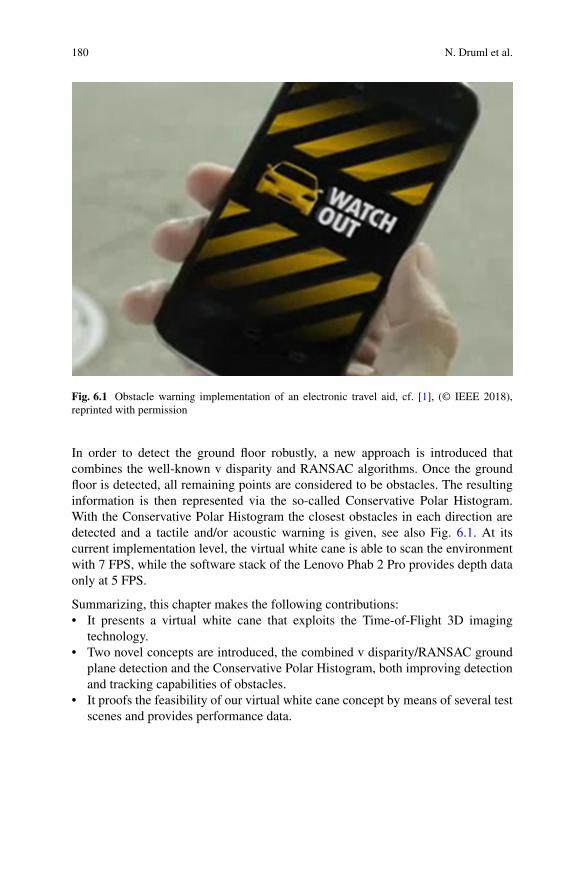
180 N. Druml et al.
Fig. 6.1 Obstacle warning implementation of an electronic travel aid, cf. [1], (© IEEE 2018),reprinted with permission
In order to detect the ground floor robustly, a new approach is introduced thatcombines the well-known v disparity and RANSAC algorithms. Once the groundfloor is detected, all remaining points are considered to be obstacles. The resultinginformation is then represented via the so-called Conservative Polar Histogram.With the Conservative Polar Histogram the closest obstacles in each direction aredetected and a tactile and/or acoustic warning is given, see also Fig. 6.1. At itscurrent implementation level, the virtual white cane is able to scan the environmentwith 7 FPS, while the software stack of the Lenovo Phab 2 Pro provides depth dataonly at 5 FPS.
Summarizing, this chapter makes the following contributions:• It presents a virtual white cane that exploits the Time-of-Flight 3D imaging
technology.• Two novel concepts are introduced, the combined v disparity/RANSAC ground
plane detection and the Conservative Polar Histogram, both improving detectionand tracking capabilities of obstacles.
• It proofs the feasibility of our virtual white cane concept by means of several testscenes and provides performance data.
6 A Smartphone-Based Virtual White Cane Prototype Featuring Time-of-. . . 181
6.2 Related Work
This section summarizes the current state-of-the-art of depth-based techniques foraiding visually impaired people. The authors in [2] divide the electronic devices fornavigation into three categories:
• Vision Enhancement: This helps users with some remaining residual vision byproviding enhanced visual output.
• Vision Replacement: This approach replaces the human vision and providesoutput directly to the optic nerve or the human brain.
• Vision Substitution: This uses other sensory means, such as auditory or tactilefeedback, in order to provide a mental image of the scene.
Vision substitution can be further subdivided in the following three maincategories:
• Electronic Travel Aid (ETA): provides information normally perceived visuallyby transforming them into a form which can be communicated through othersensory modality.
• Electronic Orientation Aid (EOA): supports the user by providing orientation aid.• Position Locator Device (PLD): provides the user with positional information,
for example, by means of GPS.
RGB-Depth (RGB-D) camera solutions are nowadays widely available, thanksto the introduction of Google Tango, Google ARCore, and Microsoft Kinectdevices. These devices either operate directly on the point cloud, for example,by using RANSAC-based algorithms, or use more complex computer vision-aidedapproaches, such as marching cubes or region growing. As an example, the systempresented by the authors in [3] directly operates in a time-critical manner on thepoint cloud. Their algorithm is therefore interruptible and shall provide conservativeand meaningful results. In [4], the authors introduced a RANSAC-based approachthat uses the point cloud data which is directly obtained from a RGB-D sensor.Aladren et al. use the RANSAC algorithm in order to fuse RGB-D data for extendingthe range of the depth sensor. They exploit a voxel-based filter in order to down-sample the point cloud, which significantly reduces the work load (7,000 pointsare considered instead of 300,000 without losing crucial information). Then, theauthors use a Manhattan world model (three main directions which are orthogonalbetween each other [5]) in order to find the most prominent planes. In [6], the authorspresented a fast plane detection solution. In their work, a Swissranger SR3000 3Drange camera was used to obtain the point cloud data. Furthermore, region growingwas employed in order to detect the planes. The authors of [7] used a differentapproach for obstacle detection: a depth map and the marching squares algorithmwere used, instead of finding structures in the point cloud. In addition, the authorsused sound output to inform the user of obstacles. While the pitch of the soundrepresents the height (y-axis), the volume represents the distance to the user, and thex position is encoded using stereo. A computer vision-based approach was presented
182 N. Druml et al.
by the authors of [8] using Microsoft’s Kinect in combination with Speeded UpRobust Feature (SURF) local descriptors that are clustered via a Bag-of-Visual-Words (BOVW) model. The BOVW constructs feature vectors that serve as inputfor a multi-class Support Vector Machine (SVM) in order to classify common officeobjects like laptops, chairs, stairs, etc. In [9], the authors used Google Tango in orderto help visually impaired users with the detection and recognition of objects andfaces. While face and object recognition were carried out via deep neural networks(NVIDIA’s CUDA Deep Neural Network Library cuDNN), the depth relation ofthese objects and faces was carried out with Google Tango’s depth data.
A revolutionary and completely new algorithm to detect the ground plane instereo images, in particular for autonomous and assisted driving, was presentedin [10]. By using the disparity map of a stereo camera, they calculated a vdisparity map. In this particular v disparity map, a ground plane is mapped toa straight line. Therefore, in order to detect such a straight line in this map, astandard Hough transformation is used. If a non-flat road geometry is given, thena succession of parts of planes is assumed. These parts of planes are given asa piecewise linear curve. Obstacles and objects are represented as vertical linesin the v disparity image. The authors of [11] enhanced the v disparity approachin order to handle also off-road scenarios. First, they used v disparity to findground plane assumption. Then, static calibration data was employed to computethe expected ground correlation line on a flat surface and the ground correlation linefor different pitch angles. Afterwards, the v disparity along these candidate lines wasaccumulated and the line with the best correlation was chosen allowing obtainingpitch estimation. Further algorithm advancements were achieved by the authors in[12]. They combined v disparity’s ability to detect the road [10] with u disparity,thus improving the ability to detect objects and obstacles. The authors proposed apropagation algorithm in order to cope with difficulties such as roll, yaw, pitch, orroad slant. In [13], the authors applied for the first time a threshold to the u disparityand thus obtained an obstacle map. By using a threshold, only obstacles with acertain height in pixels are kept. The v disparity is calculated on the free map. Thefree map is defined as every pixel that is not given as an obstacle in the obstaclemap. As a consequence, removing the pixels that are part of obstacles increases thechance of the road surface to be the most prominent line in the v disparity map.In [14], the authors demonstrated that the approach of [12] can be feasibly appliedto 3D cameras as well. They calculated the disparity by assuming a baseline of astereo-vision camera. In order to enhance the segmentation of obstacles on the road,the authors exploited both the v disparity and the u disparity. Another approach waspresented in [15]. The authors assumed that a robot/vehicle moves on the groundplane and all points detected above the ground plane can be assumed to be obstacles.Furthermore, this approach required an initial space directly in front of the robot thatis free, which is used for calibration purposes. Whenever there are more than 40%invalid depth readings, the authors assumed that it is not safe to proceed any further.
Summarizing, even though this research area is highly active, there are still lotsof gaps. Therefore, this chapter provides an innovative contribution to the ongoingdiscussion in this important field of Electronic Travel Aids.
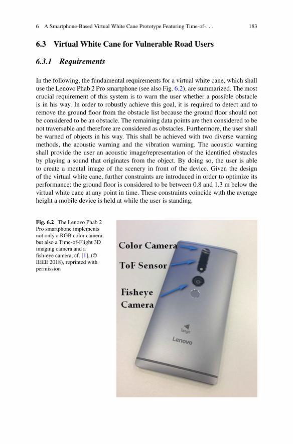
6 A Smartphone-Based Virtual White Cane Prototype Featuring Time-of-. . . 183
6.3 Virtual White Cane for Vulnerable Road Users
6.3.1 Requirements
In the following, the fundamental requirements for a virtual white cane, which shalluse the Lenovo Phab 2 Pro smartphone (see also Fig. 6.2), are summarized. The mostcrucial requirement of this system is to warn the user whether a possible obstacleis in his way. In order to robustly achieve this goal, it is required to detect and toremove the ground floor from the obstacle list because the ground floor should notbe considered to be an obstacle. The remaining data points are then considered to benot traversable and therefore are considered as obstacles. Furthermore, the user shallbe warned of objects in his way. This shall be achieved with two diverse warningmethods, the acoustic warning and the vibration warning. The acoustic warningshall provide the user an acoustic image/representation of the identified obstaclesby playing a sound that originates from the object. By doing so, the user is ableto create a mental image of the scenery in front of the device. Given the designof the virtual white cane, further constraints are introduced in order to optimize itsperformance: the ground floor is considered to be between 0.8 and 1.3 m below thevirtual white cane at any point in time. These constraints coincide with the averageheight a mobile device is held at while the user is standing.
Fig. 6.2 The Lenovo Phab 2Pro smartphone implementsnot only a RGB color camera,but also a Time-of-Flight 3Dimaging camera and afish-eye camera, cf. [1], (©IEEE 2018), reprinted withpermission
184 N. Druml et al.
6.3.2 Lenovo Phab 2 Pro Hardware
The Lenovo Phab 2 Pro is a state-of-the-art smartphone that integrates a QualcommSnapdragon 652 processor featuring an octa-core processor architecture and theAdreno 510 GPU. Its 64 bit CPU comes with the following specification: 4×1.8 GHz Coretex-A72, 4× 1.4 GHz Cortex-A53, and 4 GB RAM. In order toimplement a high-performance virtual white cane, a GPU is of high importance,because it enables the usage of Khronos OpenCL for improved computationalperformance. The Adreno GPU runs at 600 MHz and supports 128 ALUs, aunified memory, and a unified shader model. The unified memory is of particularimportance because memory can be shared between CPU and GPU which improvesthe performance of memory accesses without the need of dedicated memory copies.Typically, these memory copies represent a bottleneck of GPGPU programs. TheLenovo Phab 2 Pro’s Adreno 510 GPU supports the following APIs:
• OpenCL 2.0 Full Profile.• OpenGL ES 3.2.• OpenGL 3.2.• Vulkan 1.0.
Although Vulkan is supported by the Adreno GPU, it is not supported by Androidversion 6.0 Marshmallow that is available on the Lenovo Phab 2 Pro. Once Android7.0 Nougat will be available for the Lenovo Phab 2 Pro, also Vulkan will be fullysupported. Furthermore, there is no official support of OpenCL via Android. Yet,the Lenovo Phab 2 Pro comes with the Open CL 2.0 libraries that can be employedby developers, and which was also employed for the presented Virtual White Caneproject.
With regard to sensors, the Lenovo Phab 2 Pro integrates a 224 × 172 pixel Time-of-Flight depth camera (which was jointly developed by Infineon Technologies andPMDTechnologies), a 640 × 480 fish-eye lens camera using the software stack formotion tracking, and a high resolution 1920 × 1080 pixel RGB color camera. Inaddition, also a compass/magnetometer, proximity sensor, accelerometer, ambientlight sensor, gyroscope, and barometer are available. The Time-of-Flight camera,which represents the most crucial sensor for the Virtual White Cane, integratesa patented Suppression of Background Illumination technology. This technologyensures a robust operation not only during dark environment condition, but moreimportantly also during harsh and bright sunlight enabling outdoor operation.
6.3.3 Tilt Angle Considerations
The tilt angle of our virtual white cane device is mostly irrelevant. This is due to thefact that the angle of the line that has to be found within the v disparity map directlycorrelates directly, in a linear way, with the device’s tilt angle. By employing the
6 A Smartphone-Based Virtual White Cane Prototype Featuring Time-of-. . . 185
Lenovo Phab 2 Pro’s internal gravity sensor, the orientation of the device can bedetected and thus the angle of the line in the v disparity map can be calculated(according to Eq. (6.1) where k and d represent the parameters of the line) andfound.
angle = k ∗ tilt + d (6.1)
The parameters k and d can be found by following the following procedure:
• Record the v disparity map of an empty room without any obstacles• Employ Hough transformation in order to find lines• Record angle and tilt angle and perform a linear regression on these data points
As a result, a k value of 0.1478 and a d value of 163.223 can be found. Theseparameters together with the tilt angle enable the calculation of the line angle witha fairly tight bound. As a consequence, it is possible to allow for a deviation ofonly 1◦.
6.3.4 Basic Flow of Operations
The high-level flow of operations of the virtual white cane is depicted by Fig. 6.3.First, the VirtualWhiteCaneService connects to Android’s point cloud provider andforwards the point cloud to the GroundDetectionModule. This module calculates thev disparity map and runs RANSAC on this input data. The result is then forwardedto the WarningModule that generates the ConservativePolarHistogram and warnsthe user in case of a detected obstacle.
6.3.5 Ground Detection Module
The ground detection module does not solve the problem of finding obstacles butsolves instead the inverse problem of finding the free space in front of the user. Forthis task, the ground plane has to be detected and filtered. Any remaining points thatare not part of the ground plane are considered as obstacles. Given the applicationscenario of the virtual white cane (smartphone being held in various heights anddistances to the floor), a combination of two algorithms is used in order to improvethe robustness of detecting the ground plane. At first, the v disparity is calculatedand the line, which represents a candidate for ground plane, is found via Houghtransformation. A filter then separates the points belonging to the ground planeand the points representing obstacles. The ground plane candidate is then fed intothe RANSAC algorithm. The output of the RANSAC algorithm is then used tocrosscheck the point cloud data. In case the v disparity algorithm is not able tofind a ground plane at all, then all points are obstacles. The basic flow of this ground
186 N. Druml et al.
onTangoPointCloudAvailable()
TangoPointCloud
VirtualWhiteCaneService
GroundDetec�onWorkerThread
vDisparityMap RANSAC GroundPlane
WarningModuleThread
ObjectDetector
Acous�cWarningTac�leWarning
PointCloudProvider
GroundDetec�onModule
WarningModule
Obstacle Cloud
Conserva�ve Polar Histogram
Connects Tango Service
Fig. 6.3 Basic flow of operations of the virtual white cane, cf. [1], (© IEEE 2018), reprinted withpermission
plane detection approach is depicted in Fig. 6.4. In the following, the ground planedetection will be explained in detail.
6.3.6 v Disparity Map
The v disparity map calculation requires the point cloud to be represented in anordered (u, v) grid. After an input point cloud is ordered, the v disparity can becalculated according to the following procedure. Given disparity map I, the vdisparity map Iv is calculated by summing up the points of same disparity in Ialong the −→v axis. An example of such a v disparity map calculation is illustrated inFig. 6.5.
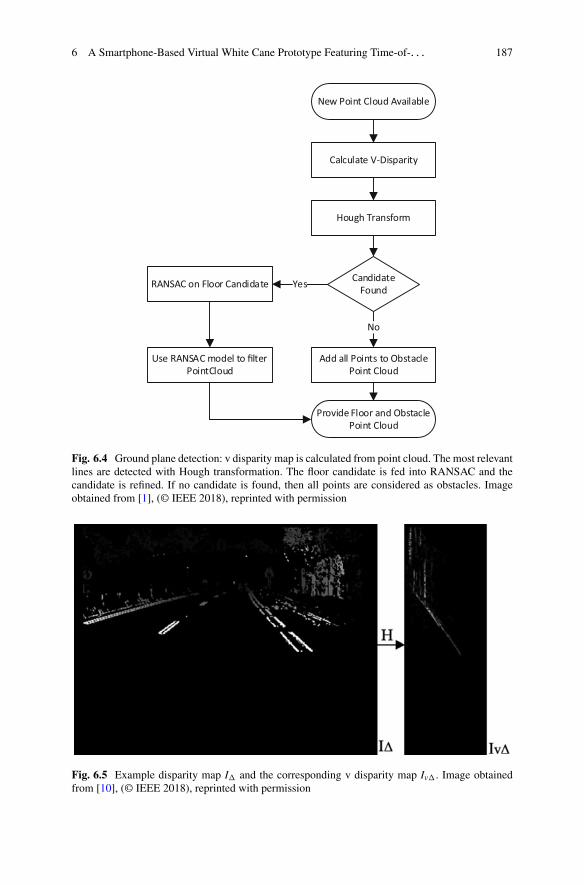
6 A Smartphone-Based Virtual White Cane Prototype Featuring Time-of-. . . 187
New Point Cloud Available
Calculate V-Disparity
Hough Transform
Candidate FoundYesRANSAC on Floor Candidate
No
Use RANSAC model to filter PointCloud
Provide Floor and Obstacle Point Cloud
Add all Points to Obstacle Point Cloud
Fig. 6.4 Ground plane detection: v disparity map is calculated from point cloud. The most relevantlines are detected with Hough transformation. The floor candidate is fed into RANSAC and thecandidate is refined. If no candidate is found, then all points are considered as obstacles. Imageobtained from [1], (© IEEE 2018), reprinted with permission
Fig. 6.5 Example disparity map I and the corresponding v disparity map Iv. Image obtainedfrom [10], (© IEEE 2018), reprinted with permission
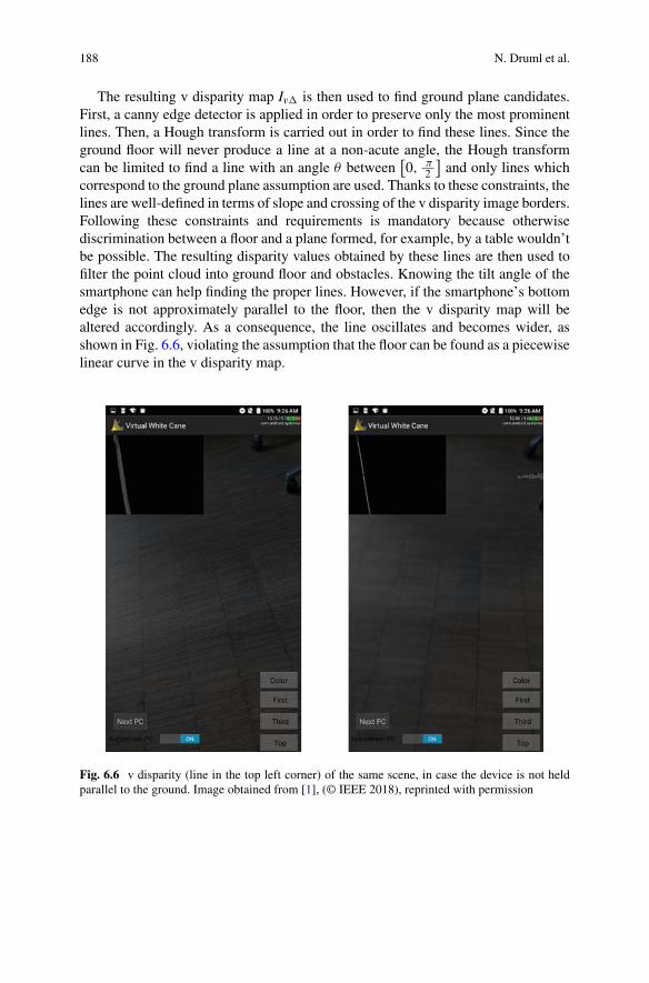
188 N. Druml et al.
The resulting v disparity map Iv is then used to find ground plane candidates.First, a canny edge detector is applied in order to preserve only the most prominentlines. Then, a Hough transform is carried out in order to find these lines. Since theground floor will never produce a line at a non-acute angle, the Hough transformcan be limited to find a line with an angle θ between
[0, π
2
]and only lines which
correspond to the ground plane assumption are used. Thanks to these constraints, thelines are well-defined in terms of slope and crossing of the v disparity image borders.Following these constraints and requirements is mandatory because otherwisediscrimination between a floor and a plane formed, for example, by a table wouldn’tbe possible. The resulting disparity values obtained by these lines are then used tofilter the point cloud into ground floor and obstacles. Knowing the tilt angle of thesmartphone can help finding the proper lines. However, if the smartphone’s bottomedge is not approximately parallel to the floor, then the v disparity map will bealtered accordingly. As a consequence, the line oscillates and becomes wider, asshown in Fig. 6.6, violating the assumption that the floor can be found as a piecewiselinear curve in the v disparity map.
Fig. 6.6 v disparity (line in the top left corner) of the same scene, in case the device is not heldparallel to the ground. Image obtained from [1], (© IEEE 2018), reprinted with permission
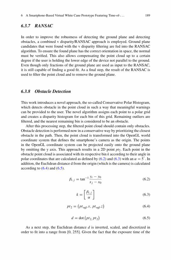
6 A Smartphone-Based Virtual White Cane Prototype Featuring Time-of-. . . 189
6.3.7 RANSAC
In order to improve the robustness of detecting the ground plane and detectingobstacles, a combined v disparity/RANSAC approach is employed. Ground planecandidates that were found with the v disparity filtering are fed into the RANSACalgorithm. To ensure the found plane has the correct orientation in space, the normalmust be verified. This also allows compensating the point cloud up to a certaindegree if the user is holding the lower edge of the device not parallel to the ground.Even though only fractions of the ground plane are used as input to the RANSAC,it is still capable of finding a good fit. As a final step, the result of the RANSAC isused to filter the point cloud and to remove the ground plane.
6.3.8 Obstacle Detection
This work introduces a novel approach, the so-called Conservative Polar Histogram,which detects obstacle in the point cloud in such a way that meaningful warningscan be provided to the user. The novel algorithm assigns each point to a polar gridand creates a disparity histogram for each bin of this grid. Remaining outliers arefiltered, and the nearest remaining bin is considered to be an obstacle.
After this processing step, the filtered point cloud should contain only obstacles.Obstacle detection is performed now in a conservative way by prioritizing the closestobstacle in the path. Then, the point cloud is transformed into the OpenGL worldcoordinate system that defines the smartphone’s camera as the origin. The pointsin the OpenGL coordinate system can be projected easily onto the ground planeby omitting the y axis. This approach results in a 2D point pt2. Each point in theobstacle point cloud is associated with its respective bin k according to their angle inpolar coordinates that are calculated as defined by (6.2) and (6.3) with an α = 5
◦. In
addition, the Euclidean distance d from the origin (which is the camera) is calculatedaccording to (6.4) and (6.5).
βi,j = tan−1 yi − y0
xj − x0(6.2)
k =[βi,j
α
](6.3)
pt2 = (ptogl.x, ptogl.z
)(6.4)
d = dot(pt2,pt2
)(6.5)
As a next step, the Euclidean distance d is inverted, scaled, and discretized inorder to fit into a range from [0, 255]. Given the fact that the exposure time of the
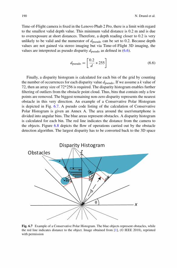
190 N. Druml et al.
Time-of-Flight camera is fixed in the Lenovo Phab 2 Pro, there is a limit with regardto the smallest valid depth value. This minimum valid distance is 0.2 m and is dueto overexposure at short distances. Therefore, a depth reading closer to 0.2 is veryunlikely to be valid and the numerator of dpseudo can be set to 0.2. Because depthvalues are not gained via stereo imaging but via Time-of-Flight 3D imaging, thevalues are interpreted as pseudo disparity dpseudo as defined in (6.6).
dpseudo =[
0.2
d∗ 255
](6.6)
Finally, a disparity histogram is calculated for each bin of the grid by countingthe number of occurrences for each disparity value dpseudo. If we assume a k value of72, then an array size of 72*256 is required. The disparity histogram enables furtherfiltering of outliers from the obstacle point cloud. Thus, bins that contain only a fewpoints are removed. The biggest remaining non-zero disparity represents the nearestobstacle in this very direction. An example of a Conservative Polar Histogramis depicted in Fig. 6.7. A pseudo code listing of the calculation of ConservativePolar Histogram is given an Annex A. The area around the user/smartphone isdivided into angular bins. The blue areas represent obstacles. A disparity histogramis calculated for each bin. The red line indicates the distance from the camera tothe objects. Figure 6.8 depicts the flow of operations carried out by the obstacledetection algorithm. The largest disparity has to be converted back to the 3D space
Disparity Histogram
Fig. 6.7 Example of a Conservative Polar Histogram. The blue objects represent obstacles, whilethe red line indicates distance to the object. Image obtained from [1], (© IEEE 2018), reprintedwith permission
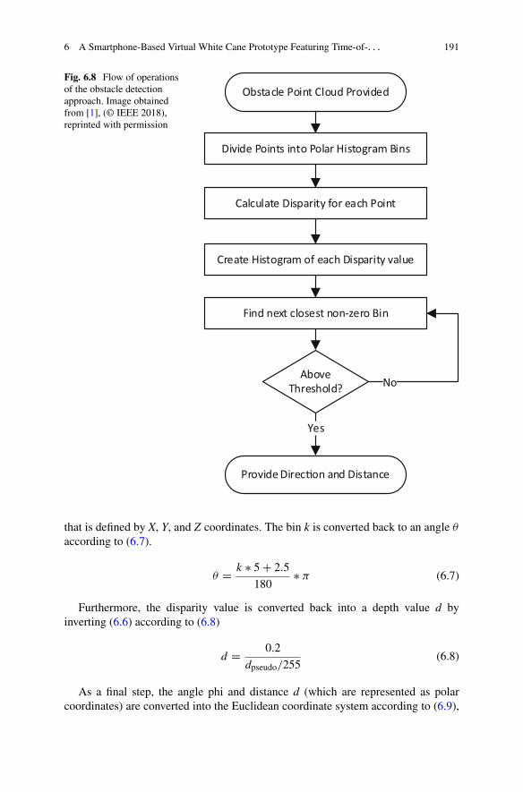
6 A Smartphone-Based Virtual White Cane Prototype Featuring Time-of-. . . 191
Fig. 6.8 Flow of operationsof the obstacle detectionapproach. Image obtainedfrom [1], (© IEEE 2018),reprinted with permission
Obstacle Point Cloud Provided
Divide Points into Polar Histogram Bins
Calculate Disparity for each Point
Create Histogram of each Disparity value
Find next closest non-zero Bin
Above Threshold?
Yes
Provide Direc�on and Distance
No
that is defined by X, Y, and Z coordinates. The bin k is converted back to an angle θ
according to (6.7).
θ = k ∗ 5 + 2.5
180∗ π (6.7)
Furthermore, the disparity value is converted back into a depth value d byinverting (6.6) according to (6.8)
d = 0.2
dpseudo/255(6.8)
As a final step, the angle phi and distance d (which are represented as polarcoordinates) are converted into the Euclidean coordinate system according to (6.9),

192 N. Druml et al.
(6.10), and (6.11). Information with regard to coordinate Y are lost due to the factthat the Conservative Polar Histogram presented in this work only supports a two-dimensional representation of the data.
X = d ∗ cos (θ) (6.9)
Z = d ∗ sin (θ) (6.10)
Y = 1 (6.11)
6.3.9 Obstacle Warning
Obstacle warning is as crucial as detecting the obstacles because if the warningcannot be easily and quickly interpreted by the user in a robust way, then a warningwill not provide any benefit at all. In principle, warnings can be generated either ina tactile or acoustic way, or by combining both methods.
The obstacle warning module receives the nearest detected obstacles from theobstacle detector module. While the acoustic warning submodule places a soundsource for each object and plays the sounds sequentially, the tactile warningsubmodule is more limited in terms of capabilities: neither the vibration’s intensitycan be modified, nor a direction can be encoded in any way. Given these constraints,a vibration warning is only provided in case an obstacle is immediately in front ofthe user.
6.3.10 Vibrator Warning
Given the highlighted constraint that the vibrator warnings in Android cannot bealtered in terms of intensity, it is only possible to provide a warning once an obstacleis within a certain distance, defined as 1 m, of the user. Furthermore, it is onlypossible to communicate a direction to the user if the virtual white cane is movedin a scanning way. Therefore, only the front facing bins of the Conservative PolarHistogram are regarded for triggering a vibrator warning. This is feasible becausethe Conservative Polar Histogram resides in a world coordinate system with thedevice rotating at the origin and the front facing bins are calculated in relation to thedevice’s orientation.
6 A Smartphone-Based Virtual White Cane Prototype Featuring Time-of-. . . 193
6.3.11 Acoustic Warning
Acoustic sounds represent an essential approach in order to warn the user ofapproaching obstacles. Thanks to stereo sound and the Head-Related TransferFunction (HRTF), a source of sound can be positioned in a certain direction to theuser. Therefore, an approaching obstacle can be located by the user in its direction.
The Acoustic Warning module positions a source of sound for each bin of theConservative Polar Histogram if a certain distance limit is reached. These soundsare played sequentially like sonar/radar, which enables the visually impaired personto create a mental image of the surroundings with its obstacles. Experiments withacoustic warnings showed that choosing the right sound to play is not a trivialselection. While such a sound shall not only be easily differentiable from anynatural sound source, it shall also contain various frequencies instead of only asimple sine wave. This is due to the fact that the more complex a sound is, theeasier is the localization of such a sound. However, a sound shall not be playedtoo long because several sound sources will overlap due to the sonar/radar likeplaystyle. The Acoustic Warning module plays the sounds in a repeating and roundrobin fashion, which creates an animated impression (the sound moves along theobstacles). Repeating and animated sounds help the visually impaired person topinpoint obstacles much faster.
6.4 Results
In this section, the results and the performance of the Virtual White Cane arediscussed. In the following figures, the color of the pixels defines their classificationafter the ground detection algorithm. While green pixels represent the ground plane,red pixels indicate detected obstacles.
Our proposed combination of v Disparity and RANSAC algorithms improvessignificantly the accuracy of a pure RANSAC approach. Due to RANSAC’s randomapproach and fitting process, the best resulting fit is not always reflecting the realscenery. This behavior is shown in Fig. 6.9. While the RANSAC shows a poorlyfitting ground plane, our approach (which combines RANSAC with v Disparity)detects the ground plane and the obstacles properly. Our combined RANSAC/vDisparity approach also overcomes problems with cluttered scenes, as demonstratedin Fig. 6.10.
The v disparity segmentation algorithm often classifies too many points asground plane, while RANSAC is unable to find a properly fitting plane. This isthe case for example if a large obstacle is covering most of the floor. Figure 6.11illustrates this situation. While RANSAC is not able to detect the correct floor at all,v disparity can clearly identify the floor. Again, our approach that combines bothalgorithms can robustly detect the floor and the scenery’s obstacles.
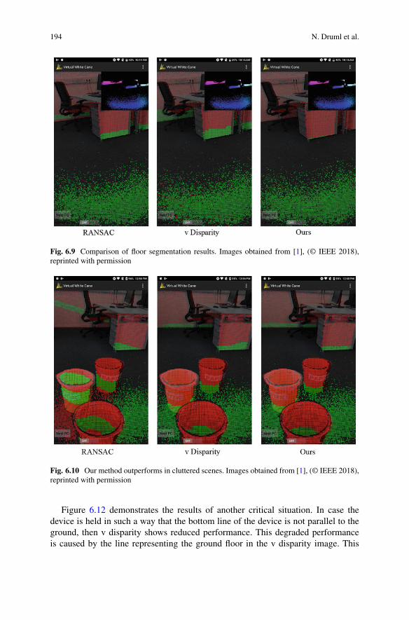
194 N. Druml et al.
Fig. 6.9 Comparison of floor segmentation results. Images obtained from [1], (© IEEE 2018),reprinted with permission
Fig. 6.10 Our method outperforms in cluttered scenes. Images obtained from [1], (© IEEE 2018),reprinted with permission
Figure 6.12 demonstrates the results of another critical situation. In case thedevice is held in such a way that the bottom line of the device is not parallel to theground, then v disparity shows reduced performance. This degraded performanceis caused by the line representing the ground floor in the v disparity image. This
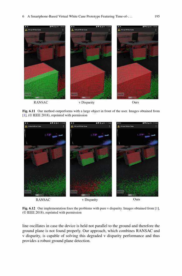
6 A Smartphone-Based Virtual White Cane Prototype Featuring Time-of-. . . 195
Fig. 6.11 Our method outperforms with a large object in front of the user. Images obtained from[1], (© IEEE 2018), reprinted with permission
Fig. 6.12 Our implementation fixes the problems with pure v disparity. Images obtained from [1],(© IEEE 2018), reprinted with permission
line oscillates in case the device is held not parallel to the ground and therefore theground plane is not found properly. Our approach, which combines RANSAC andv disparity, is capable of solving this degraded v disparity performance and thusprovides a robust ground plane detection.
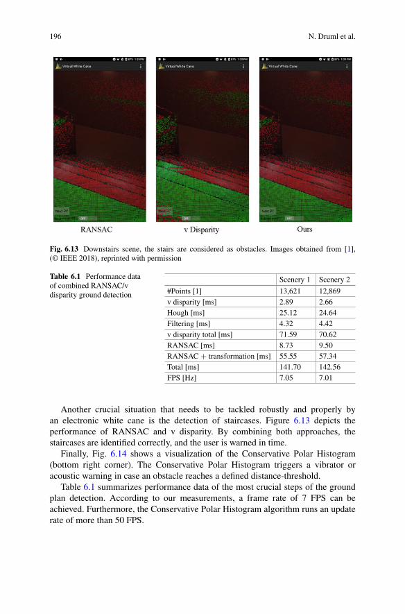
196 N. Druml et al.
Fig. 6.13 Downstairs scene, the stairs are considered as obstacles. Images obtained from [1],(© IEEE 2018), reprinted with permission
Table 6.1 Performance dataof combined RANSAC/vdisparity ground detection
Scenery 1 Scenery 2
#Points [1] 13,621 12,869v disparity [ms] 2.89 2.66Hough [ms] 25.12 24.64Filtering [ms] 4.32 4.42v disparity total [ms] 71.59 70.62RANSAC [ms] 8.73 9.50RANSAC + transformation [ms] 55.55 57.34Total [ms] 141.70 142.56FPS [Hz] 7.05 7.01
Another crucial situation that needs to be tackled robustly and properly byan electronic white cane is the detection of staircases. Figure 6.13 depicts theperformance of RANSAC and v disparity. By combining both approaches, thestaircases are identified correctly, and the user is warned in time.
Finally, Fig. 6.14 shows a visualization of the Conservative Polar Histogram(bottom right corner). The Conservative Polar Histogram triggers a vibrator oracoustic warning in case an obstacle reaches a defined distance-threshold.
Table 6.1 summarizes performance data of the most crucial steps of the groundplan detection. According to our measurements, a frame rate of 7 FPS can beachieved. Furthermore, the Conservative Polar Histogram algorithm runs an updaterate of more than 50 FPS.
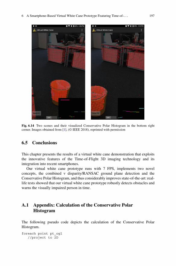
6 A Smartphone-Based Virtual White Cane Prototype Featuring Time-of-. . . 197
Fig. 6.14 Two scenes and their visualized Conservative Polar Histogram in the bottom rightcorner. Images obtained from [1], (© IEEE 2018), reprinted with permission
6.5 Conclusions
This chapter presents the results of a virtual white cane demonstration that exploitsthe innovative features of the Time-of-Flight 3D imaging technology and itsintegration into recent smartphones.
Our virtual white cane prototype runs with 7 FPS, implements two novelconcepts, the combined v disparity/RANSAC ground plane detection and theConservative Polar Histogram, and thus considerably improves state-of-the-art: real-life tests showed that our virtual white cane prototype robustly detects obstacles andwarns the visually impaired person in time.
A.1 Appendix: Calculation of the Conservative PolarHistogram
The following pseudo code depicts the calculation of the Conservative PolarHistogram.
foreach point pt_ogl//project to 2D

198 N. Druml et al.
pt_2 = (pt_ogl.x, pt_ogl.z);
// calculate angle beta and bin number// e.g. ALPHA = 5 degreesbeta = atan(pt_2.x / pt_2.z);k = beta/ALPHA;
// calculate distance and pseudo disparityd = dot(pt_2, pt_2);d_pseudo = floor(0.2/distance * 255);
// use k and d_pseudo to increment the histogram valuedisparityHistogram[k][d_pseudo]++;
Glossary
BOVW Bag-of-Visual-WordsETA Electronic Travel AidEOA Electronic Orientation AidFOV Field of ViewGPGPU General Purpose Graphics Processing UnitHRTF Head-Related Transfer FunctionPLD Position Locator DeviceRANSAC RANdom SAmple ConsensusRGB-D Color and Depth sensing CameraSURF Speeded Up Robust FeatureSVM Support Vector MachineToF Time-of-Flight
Acknowledgements This project has received funding from the Electronic Component Systemsfor European Leadership Joint Undertaking under grant agreement No 692480. This JointUndertaking receives support from the European Union’s Horizon 2020 research and innovationprogram and Germany, Netherlands, Spain, Austria, Belgium, and Slovakia.
References
1. N. Druml, T. Pietsch, M. Dielacher, C. Steger, M. Baumgart, C. Consani, T. Herndl, G. Holweg,Virtual white cane featuring time-of-flight 3D imaging supporting visually impaired users, in2018 21st Euromicro Conference on Digital System Design (DSD), (2018), pp. 450–457
2. D. Dakopoulos, N.G. Bourbakis, Wearable obstacle avoidance electronic travel aids for blind:A survey. IEEE Trans. Syst. Man Cybern. Part C Appl. Rev. 40(1), 25–35 (2010)
3. D. Bernabei, F. Ganovelli, M.D. Benedetto, M. Dellepiane, R. Scopigno, A low-cost time-critical obstacle avoidance system for the visually impaired, in International Conference onIndoor Positioning and Indoor Navigation, (2011), pp. 21–23

6 A Smartphone-Based Virtual White Cane Prototype Featuring Time-of-. . . 199
4. M. Vlaminck, L. Jovanov, P. Van Hese, B. Goossens, W. Philips, A. Pizurica, Obstacledetection for pedestrians with a visual impairment based on 3D imaging, in 2013 InternationalConference on 3D Imaging, (2013)
5. J.M. Coughlan, A. Yuille, Manhattan world: Compass direction from a single image byBayesian inference, in Proceedings of the Seventh IEEE International Conference on ComputerVision, vol. 2, (1999)
6. J. Poppinga, N. Vaskevicius, A. Birk, K. Pathak, Fast plane detection and polygonalization innoisy 3D range images, in 2008 IEEE/RSJ International Conference on Intelligent Robots andSystems, IROS, (2008), pp. 3378–3383
7. M. Brock, P.O. Kristensson, Supporting blind navigation using depth sensing and sonification,in Proceedings of the 2013 ACM Conference on Pervasive and Ubiquitous Computing AdjunctPublication—UbiComp ‘13 Adjunct, (2013)
8. A. Bhowmick, S. Prakash, R. Bhagat, V. Prasad, S. M. Hazarika, IntelliNavi: Navigationfor blind based on kinect and machine learning, in Multi-disciplinary Trends in ArtificialIntelligence (2014)
9. R. Jafri, A GPU-accelerated real-time contextual awareness application for the visuallyimpaired on Google’s project Tango device (2016)
10. R. Labayrade, D. Aubert, J.-P. Tarel, Real Time Obstacle Detection in Stereovision on Non FlatRoad Geometry Through “v-disparity” Representation, vol 2 (2002), pp. 646–651
11. A. Broggi, C. Caraffi, R.I. Fedriga, P. Grisleri, Obstacle detection with stereo vision for off-road vehicle navigation, in 2005 IEEE Computer Society Conference on Computer Vision andPattern Recognition (CVPR’05)-Workshops, (2005), p. 65
12. N. Soquet, D. Aubert, N. Hautiere, Road Segmentation Supervised by an Extended V-DisparityAlgorithm for Autonomous Navigation (2007), pp. 160–165
13. B. Musleh, A. De La Escalera, J.M. Armingol, U-V disparity analysis in urban environments,in Lecture Notes in Computer Science, vol. 6928, (2012), pp. 426–432
14. Y. Gao, X. Ai, J. Rarity, N. Dahnoun, Obstacle detection with 3D camera using U-V-disparity,in International Workshop on Systems, Signal Processing and Their Applications, WOSSPA,(2011)
15. B. Peasley, S.T. Birchfield, Real-time obstacle detection and avoidance in the presence ofspecular surfaces using an active 3D sensor, in 2013 IEEE Workshop on Robot Vision (WORV),(2013)
Chapter 7Power Consumption Minimizationof Wireless Sensor Networksin the Internet of Things Era
Jordi Serra, David Pubill, and Christos Verikoukis
7.1 Introduction
WSN are key components of the upcoming IoT revolution, where billions of deviceswith sensing, communications, and actuating capabilities will set up a huge geo-distributed perception system to interact with the background. Thereby, IoT createsa plethora of applications such as air quality monitoring in smart cities and self-driving cars. However, IoT benefits may be impaired by the limited energy budget ofbattery-powered WSN devices. Energy constraints limit the WSN devices lifetime,which leads to a performance loss in an IoT application. Moreover, the limitedenergy budget provokes the battery replenishment of a huge number of WSN devicesand increases the maintenance cost.
Therefore, this chapter proposes methods for an efficient management of theWSN nodes’ power consumption. In the first part, two techniques are jointlyconsidered to reduce the transmitted power of the WSN nodes to achieve a desiredquality of service at the receiver side, which is measured in terms of the MeanSquare Error (MSE) in the estimation of the Signal of Interest (SoI). The first ofthese techniques is a power allocation method at each WSN node, i.e., a weight thatcontrols the transmitted power. Namely, this weight takes into account whether thereis redundant information among WSN nodes, the quality of measurement, and thequality of the wireless link between the WSN node and the access point (AP). Thesecond technique considers the use of multiple distributed APs at the receiver sideto decrease the transmitted power. Numerical simulations have been carried out tovalidate the proposed methods. These simulations highlight that if power allocationat each WSN node is jointly used with multiple APs, then it is possible to reduce
J. Serra (�) · D. Pubill · C. VerikoukisTelecommunications Technological Center of Catalonia (CTTC), Castelldefels, Spaine-mail: [email protected]; [email protected]; [email protected]
© Springer Nature Switzerland AG 2020W. D. van Driel et al. (eds.), Sensor Systems Simulations,https://doi.org/10.1007/978-3-030-16577-2_7
201
202 J. Serra et al.
drastically the WSN nodes’ transmitted power required to achieve a target qualityof service.
In the second part, we evaluate the use of artificial light EH to power perpetuallythe WSN nodes. Namely, we propose an experimental setup for the EH of a WSNnode. The EH module consists of a Photovoltaic (PV) cell that harvests artificiallight from a nearby lamp, a boost converter that transforms the gathered energyinto the proper electrical features of the WSN node and a 3 V rechargeable coinbattery that stores the electrical energy. This EH module is the power supply fora commercial WSN node, a Zolertia Z1 WSN node. A proper configuration wasfound to power perpetually the WSN node in three different scenarios: (1) noactivity in the mote, (2) performing a simple computation, and (3) transmitting atemperature reading over the air to another WSN node. To achieve this aim, severaltransmission time periods have been considered and it has been concluded that itis possible to extend the WSN node lifetime without bound, when the transmissiontime period is above a certain threshold. Moreover, it has been studied which is themost appropriate rechargeable coin battery for the setup.
7.2 Employing Multiple Access Points and a PowerAllocation to Reduce the Transmit Power in WSN
7.2.1 Introduction
WSN have been widely used for decentralized inference tasks. Moreover, they are ofparamount importance in disruptive technologies such as IoT. WSN are composedof sensor nodes, which have a limited energy budget, as they are usually batterypowered. Thus, the design of inference problems in WSN incorporates the energyefficiency as an objective. Herein, the energy efficient estimation of a source vectorobserved by a WSN is considered. Several algorithms have been proposed to tacklethe energy efficient estimation problem. The authors in [1] studied the quantizationof the WSN data measurements. A method based on sensor selection was introducedin [2]. It minimizes the estimation error subject to an energy budget constraint.Data reduction algorithms, which rely on a linear compression of sensor nodes’data, were proposed in [3, 4] bearing in mind its influence on the estimation error.The authors in [5] considered a multiple antenna Fusion Centre (FC) scenario andproposed a power allocation at each sensor node to minimize the MSE subject topower constraints.
Actually, Energy Efficiency (EE) is a cornerstone in future wireless communi-cations systems [6]. Namely, the capacity needs to increase dramatically withoutincreasing the current power consumption substantially to avoid economical andsocietal issues. Thus, new system architectures were proposed recently to increasethe EE through a network densification, i.e., increasing the number of access pointsor communication links per unit area [6, 7]. One of them is collocated massive
7 Power Consumption Minimization of Wireless Sensor Networks. . . 203
Multiple Input Multiple Output (CM-MIMO), which relies on a large number ofantennas at the base station (BS) [8]. This system architecture was recently studiedin WSN to reduce the transmitted power in estimation tasks. Namely, consideringa coherent Multiple Access Channel (MAC), [9, 10] dealt with the MaximumLikelihood (ML) and Linear Minimum Mean Square Error (LMMSE) estimationof a scalar parameter at the FC, respectively. Within this setting [11] studied theLMMSE estimation of a correlated source vector.
Herein, multiple distributed access points and a power allocation technique arejointly used to reduce dramatically the WSN transmit power for a given estimationquality at the receiver side. The idea is that increasing the number of virtual antennasat the fusion center leads to reduce the transmit power of the WSN. Thereby, hereinthe problem of estimating a correlated source vector in a Distributed Massive-MIMO (DM-MIMO) architecture is tackled and an LMMSE estimator is proposedto achieve this aim. Namely, a WSN obtains noisy measurements of the sourcevector and sends them through a coherent MAC channel to the FC. The FC ismade of a large number of single antenna APs, which are connected to a CentralProcessing Unit (CPU) by means of a backhaul network. The LMMSE estimationis performed at the CPU. Moreover, a power allocation technique is considered ateach WSN node to minimize the total transmitted power subject to an estimationerror constraint. Thereby unlike the related works in [9–11] a DM-MIMO systemis proposed herein to carry out the estimation. These type of systems, a.k.a. largedistributed antenna systems (L-DAS), have been considered recently to increasedramatically the EE in 5G networks, see e.g., [7] or [12]. The contributions are asfollows. First, the MSE associated to the LMMSE estimation is obtained as well asan approximation of it, bearing in mind the DM-MIMO context. This paves the wayto obtain the optimal power allocation that minimizes the total transmitted power fora given estimation error as an SDP problem. The numerical simulations show thatin comparison to [11], which considers a CM-MIMO, the total WSN transmittedpower is reduced for a given MSE constraint, both in the uniform and the optimalpower allocation problems. Moreover, the work herein is more general than the onein [9, 10] as a vector source is tackled in the estimation rather than a scalar. Last butnot least, it is important to say that the proposed power allocation method can stillbe used in a distributed MIMO system, with a moderate number of virtual antennas.The difference is that in this case the power allocation is suboptimal, as it is derivedassuming a large number of virtual antennas.
7.2.2 System Model
The proposed system model is depicted in Fig. 7.1. More specifically, a WSNcomposed of L sensor nodes that takes noisy observations of a source vector θ isconsidered. The vector of measurements x is linearly modelled as
x = θ + n,
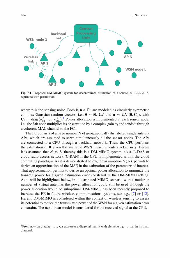
204 J. Serra et al.
Backhaulnet
AP N
CentralProcessing
UnitWSN node 1
Wireless link
WSN node L
AP 2
AP 1
Fig. 7.1 Proposed DM-MIMO system for decentralized estimation of a source. © IEEE 2018,reprinted with permission
where n is the sensing noise. Both θ, n ∈ CL are modeled as circularly symmetric
complex Gaussian random vectors, i.e., θ ∼ (0, Cθ) and n ∼ CN (0, Cn), withCn = diag
(σ 2
n1, . . . , σ2nL
).1 Power allocation is implemented at each sensor node,
i.e., the l-th node multiplies its observation by a complex gain αl and sends it througha coherent MAC channel to the FC.
The FC consists of a large number N of geographically distributed single antennaAPs, which are assumed to serve simultaneously all the sensor nodes. The APsare connected to a CPU through a backhaul network. Then, the CPU performsthe estimation of θ given the available WSN measurements stacked in y. Hereinit is assumed that N � L, thereby this is a DM-MIMO system, a.k.a. L-DAS orcloud radio access network (C-RAN) if the CPU is implemented within the cloudcomputing paradigm. As it is demonstrated below, the assumption N � L permits toderive an approximation of the MSE in the estimation of the parameter of interest.That approximation permits to derive an optimal power allocation to minimize thetransmit power for a given estimation error constraint in the DM-MIMO setting.As it will be highlighted below, in a distributed MIMO scenario with a moderatenumber of virtual antennas the power allocation could still be used although thepower allocation would be suboptimal. DM-MIMO has been recently proposed toincrease the EE in future wireless communications systems, see e.g., [7] or [12].Herein, DM-MIMO is considered within the context of wireless sensing to assessits potential to reduce the transmitted power of the WSN for a given estimation errorconstraint. The next linear model is considered for the received signal at the CPU,
1From now on diag(x1, . . . , xn) expresses a diagonal matrix with elements x1, . . . , xn in its maindiagonal.

7 Power Consumption Minimization of Wireless Sensor Networks. . . 205
y = HDx + v (7.1)
where D = diag(α1, . . . , αL) is the matrix of gains to be designed, i.e., the oneimplementing the power allocation. v ∼ CN (0, σv
2I) is an Additive White GaussianNoise (AWGN) and H ∈ C
N × L is the channel between the sensor nodes and theAPs. Note that the l-th column of H is the channel between the l-th sensor node andeach of the APs and it is modeled as follows:
H = (h1, . . . , hL) , hl = �l1/2fl (7.2)
where �l1/2 is a diagonal matrix modeling the large-scale fading, i.e.,
�l � diag(γ 1l, . . . , γ Nl), γ nl = dnl−2β , dnl is the distance between the l-th
sensor node and the n-th AP and β is the pathloss exponent. The small-scalefading is modeled by fl whose components are i.i.d random variables, namely[fl]i ∼ CN (0, 1) ∀i = 1, . . . , N .
Remark 1 A set of assumptions are made in the proposed DM-MIMO system.Firstly, as stated in, e.g., [12], a perfect backhaul network is presumed betweenthe APs and the CPU. Secondly, perfect synchronization is assumed between theWSN nodes and the APs. This allows a coherent reception at the FC, similarly thanin [11]. Thirdly, the FC has perfect knowledge of the channel and noise statistics.
Remark 2 The channel model in Eq. (7.2) highlights that the proposed DM-MIMOgeneralizes the CM-MIMO system in [11]. That is, when all the antennas arecollocated at a given AP, then the distance between the l-th sensor node and anyof the antennas is approximately the same, i.e., the elements of �l
1/2 in Eq. (7.2)can be approximated as γ nl = γ l ∀n = 1, . . . , N. This leads to obtain the channelmodel for a CM-MIMO proposed in Eq. (3) of [11].
7.2.3 Optimal Power Allocation in a DM-MIMO System
7.2.3.1 LMMSE Estimation and Asymptotic MSE Approximation
This section treats the LMMSE estimation of the SoI θ for the system architectureproposed in Sect. 7.2.2. That is, the signal received at the CPU has the model statedin Eq. (7.1) with the assumptions described in Remark 1. Furthermore, recall thatthe LMMSE estimation of θ is given by the conditional expectation θ = E [θ|y, H]see Chap. 15 in [13]. Thereby, in a DM-MIMO setting θ has the next expression
θ = E [θ|y, H] =(
C−1θ + DH HH C−1
w HD)−1
DH HH C−1w y (7.3)
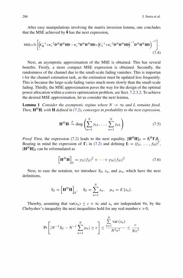
206 J. Serra et al.
After easy manipulations involving the matrix inversion lemma, one concludesthat the MSE achieved by θ has the next expression,
MSE=Tr
[(C−1
θ+σ−2
v DH HH HD − σ−4v DH HH HD×
(C−1
n +σ−2v DH HH HD
)−1DH HH HD
)−1]
.
(7.4)
Next, an asymptotic approximation of the MSE is obtained. This has severalbenefits. Firstly, a more compact MSE expression is obtained. Secondly, therandomness of the channel due to the small-scale fading vanishes. This is important for the channel estimation task, as the estimation must be updated less frequently.This is because the large-scale fading varies much more slowly than the small-scalefading. Thirdly, the MSE approximation paves the way for the design of the optimalpower allocation within a convex optimization problem, see Sect. 7.2.3.2. To achievethe desired MSE approximation, let us consider the next lemma,
Lemma 1 Consider the asymptotic regime where N → ∞ and L remains fixed.Then, HHH, with H defined in (7.2), converges in probability to the next expression,
HH Hp→ diag
(N∑
n=1
γn1, . . . ,
N∑
n=1
γnL
)(7.5)
Proof First, the expression (7.2) leads to the next equality, [HHH]ll = flH�lfl..
Bearing in mind the expression of �l in (7.2) and defining fl = (f1l, . . . , fNl)T ,[HHH]ll can be reformulated as
[HH H
]
ll= γ1l |f1l |2 + · · · + γNl |fNl |2 (7.6)
Next, to ease the notation, we introduce Sll, xn, and μn, which have the nextdefinitions,
Sll =[HH H
]
ll, Sll =
N∑
n=1
xn, μn = E [xn] .
Thereby, assuming that var(xn) ≤ c < ∞ and xn are independent ∀n, by theChebyshev’s inequality the next inequalities hold for any real number ε > 0,
Pr
[|N−1Sll − N−1
N∑
n=1
μn| ≥ ε
]≤
N∑n=1
var (xn)
N2ε2≤ c
Nε2

7 Power Consumption Minimization of Wireless Sensor Networks. . . 207
Note that μn = [γ nl|fnl|2] = γ nl, as fnl ∼ (0, 1). Thereby, taking N → ∞ in bothsides of the last expression, the next convergence in probability is obtained,
limN→∞ Pr
[|N−1Sll − N−1
N∑
n=1
γnl | ≥ ε
]= 0 (7.7)
The same procedure can be followed to demonstrate that the off diagonalelements of HHH converge to 0. To this end, observe that [HHH]lk = fl
H�l1/2�k
1/2fk
and bear in mind that fl, fk are independent with zero mean elements.Lemma 1 paves the way to obtain the desired approximation for the MSE. This
is formally stated in the next theorem.
Theorem 1 Let define the diagonal matrix B with diagonal elements bl =|αl |2∑N
n=1γnl for l = 1, . . . , L. Then, when N → ∞ for a fixed L, the MSE in(7.4) converges in probability to MSE, whose expression is given next,
MSEp→ MSE = Tr
[(C−1
θ + σ−2v B − σ−4
v B ×(
C−1n + σ−2
v B)−1
B)−1
].
(7.8)
Proof Equation (7.8) is obtained by applying Lemma 1 into Eq. (7.4).
7.2.3.2 Optimal Power Allocation
The energy is a limited resource in a WSN and the proposed DM-MIMO archi-tecture permits to reduce notably the WSN power consumption by having alarge number of virtual antennas at the FC. Thus, this section faces the problemof minimizing the total transmitted power Pt of the WSN nodes for a givenperformance constraint in the estimation procedure, within the DM-MIMO contextproposed herein.2 This problem is stated as,
minimize{bl≥0}L
l=1
Pt (bl)
subject to MSE (bl) ≤ δ
. (7.9)
where δ is the maximum allowable estimation error in the estimation task at handand the MSE approximation, i.e., MSE (bl) in Eq. (7.8), is considered. This will pavethe way to reformulate Eq. (7.9) as a convex optimization problem. Furthermore,
2It is worth saying that in a distributed MIMO scenario with a moderate number of APs, thetransmitted power of the WSN can still be reduced. Actually, the power allocation proposed in thissection still holds in that scenario, but it is suboptimal, as the MSE approximation in Eq. (7.8)requires a large number of APs.
208 J. Serra et al.
according to Sect. 7.2.2, Pt(bl) has the expression,
Pt (bl) = E
[‖D (θ + n)‖2
]T r[DH D (Cθ + Cn)
](7.10)
Now, let us define � as
� = diag
(N∑
n=1
γn1, . . . ,
N∑
n=1
γnL
)
Given this definition of � and bearing in mind the expression of bl in Theorem 1leads to express Pt(bl) as follows:
Pt (bl) = Tr[�
−1B (Cθ + Cn)
](7.11)
Thus, the optimization problem Eq. (7.9) can be reformulated as follows aftersubstituting Eqs. (7.11) and (7.8) into it,
minimizeB≥0
Tr[�
−1B (Cθ + Cn)
]
subject to Tr
[(C−1
θ + σ−2v B − σ−4
v B × (C−1
n + σ−2v B
)−1B)−1
]≤ δ
. (7.12)
Next, after introducing slack variables X, Z and by considering the Schurcomplement of a block matrix, (7.12) can be rewritten as follows:
minimizeB,X,Z≥0
Tr[�
−1B (Cθ + Cn)
]
subject to Tr [Z] ≤ δ(C−1
θ + σ−2v B − σ−4
v X II Z
)≥ 0
(X BB C−1
n + σ−2v B
)≥ 0
. (7.13)
This is an SDP problem and thereby can be solved efficiently, i.e., in polynomialtime, by software packages relying on interior point methods.
Remark 3 The comparison of the proposed algorithm in eq. (7.13) to a uniformpower allocation algorithm is of paramount importance. This is presented in Sect.7.2.4. In the latter case, D = αI and thus B = |α|2� and Pt = Tr[|α|2(Cθ+Cn)] inEq. (7.13).
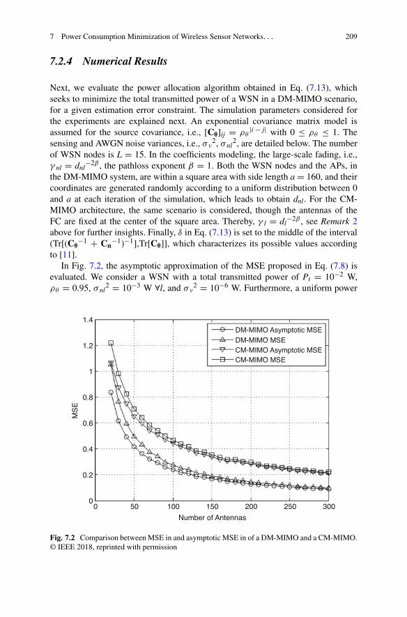
7 Power Consumption Minimization of Wireless Sensor Networks. . . 209
7.2.4 Numerical Results
Next, we evaluate the power allocation algorithm obtained in Eq. (7.13), whichseeks to minimize the total transmitted power of a WSN in a DM-MIMO scenario,for a given estimation error constraint. The simulation parameters considered forthe experiments are explained next. An exponential covariance matrix model isassumed for the source covariance, i.e., [Cθ]ij = ρθ
|i − j| with 0 ≤ ρθ ≤ 1. Thesensing and AWGN noise variances, i.e., σ v
2, σ nl2, are detailed below. The number
of WSN nodes is L = 15. In the coefficients modeling, the large-scale fading, i.e.,γ nl = dnl
−2β , the pathloss exponent β = 1. Both the WSN nodes and the APs, inthe DM-MIMO system, are within a square area with side length a = 160, and theircoordinates are generated randomly according to a uniform distribution between 0and a at each iteration of the simulation, which leads to obtain dnl. For the CM-MIMO architecture, the same scenario is considered, though the antennas of theFC are fixed at the center of the square area. Thereby, γ l = dl
−2β , see Remark 2above for further insights. Finally, δ in Eq. (7.13) is set to the middle of the interval(Tr[(Cθ
−1 + Cn−1)−1],Tr[Cθ]], which characterizes its possible values according
to [11].In Fig. 7.2, the asymptotic approximation of the MSE proposed in Eq. (7.8) is
evaluated. We consider a WSN with a total transmitted power of Pt = 10−2 W,ρθ = 0.95, σ nl
2 = 10−3 W ∀l, and σ v2 = 10−6 W. Furthermore, a uniform power
1.4
1.2
1
0.8
MS
E
0.6
0.4
0.2
00 50 100 150
Number of Antennas
DM-MIMO Asymptotic MSE
CM-MIMO Asymptotic MSEDM-MIMO MSE
CM-MIMO MSE
200 250 300
Fig. 7.2 Comparison between MSE in and asymptotic MSE in of a DM-MIMO and a CM-MIMO.© IEEE 2018, reprinted with permission
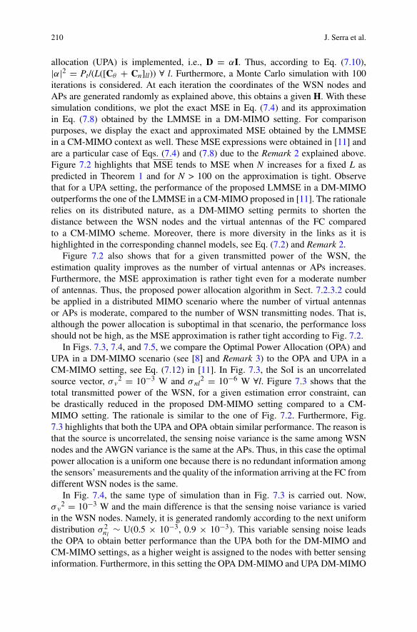
210 J. Serra et al.
allocation (UPA) is implemented, i.e., D = αI. Thus, according to Eq. (7.10),|α|2 = Pt/(L([Cθ + Cn]ll)) ∀ l. Furthermore, a Monte Carlo simulation with 100iterations is considered. At each iteration the coordinates of the WSN nodes andAPs are generated randomly as explained above, this obtains a given H. With thesesimulation conditions, we plot the exact MSE in Eq. (7.4) and its approximationin Eq. (7.8) obtained by the LMMSE in a DM-MIMO setting. For comparisonpurposes, we display the exact and approximated MSE obtained by the LMMSEin a CM-MIMO context as well. These MSE expressions were obtained in [11] andare a particular case of Eqs. (7.4) and (7.8) due to the Remark 2 explained above.Figure 7.2 highlights that MSE tends to MSE when N increases for a fixed L aspredicted in Theorem 1 and for N > 100 on the approximation is tight. Observethat for a UPA setting, the performance of the proposed LMMSE in a DM-MIMOoutperforms the one of the LMMSE in a CM-MIMO proposed in [11]. The rationalerelies on its distributed nature, as a DM-MIMO setting permits to shorten thedistance between the WSN nodes and the virtual antennas of the FC comparedto a CM-MIMO scheme. Moreover, there is more diversity in the links as it ishighlighted in the corresponding channel models, see Eq. (7.2) and Remark 2.
Figure 7.2 also shows that for a given transmitted power of the WSN, theestimation quality improves as the number of virtual antennas or APs increases.Furthermore, the MSE approximation is rather tight even for a moderate numberof antennas. Thus, the proposed power allocation algorithm in Sect. 7.2.3.2 couldbe applied in a distributed MIMO scenario where the number of virtual antennasor APs is moderate, compared to the number of WSN transmitting nodes. That is,although the power allocation is suboptimal in that scenario, the performance lossshould not be high, as the MSE approximation is rather tight according to Fig. 7.2.
In Figs. 7.3, 7.4, and 7.5, we compare the Optimal Power Allocation (OPA) andUPA in a DM-MIMO scenario (see [8] and Remark 3) to the OPA and UPA in aCM-MIMO setting, see Eq. (7.12) in [11]. In Fig. 7.3, the SoI is an uncorrelatedsource vector, σ v
2 = 10−3 W and σ nl2 = 10−6 W ∀l. Figure 7.3 shows that the
total transmitted power of the WSN, for a given estimation error constraint, canbe drastically reduced in the proposed DM-MIMO setting compared to a CM-MIMO setting. The rationale is similar to the one of Fig. 7.2. Furthermore, Fig.7.3 highlights that both the UPA and OPA obtain similar performance. The reason isthat the source is uncorrelated, the sensing noise variance is the same among WSNnodes and the AWGN variance is the same at the APs. Thus, in this case the optimalpower allocation is a uniform one because there is no redundant information amongthe sensors’ measurements and the quality of the information arriving at the FC fromdifferent WSN nodes is the same.
In Fig. 7.4, the same type of simulation than in Fig. 7.3 is carried out. Now,σ v
2 = 10−3 W and the main difference is that the sensing noise variance is variedin the WSN nodes. Namely, it is generated randomly according to the next uniformdistribution σ 2
nl∼ U(0.5 × 10⁻³, 0.9 × 10⁻³). This variable sensing noise leads
the OPA to obtain better performance than the UPA both for the DM-MIMO andCM-MIMO settings, as a higher weight is assigned to the nodes with better sensinginformation. Furthermore, in this setting the OPA DM-MIMO and UPA DM-MIMO
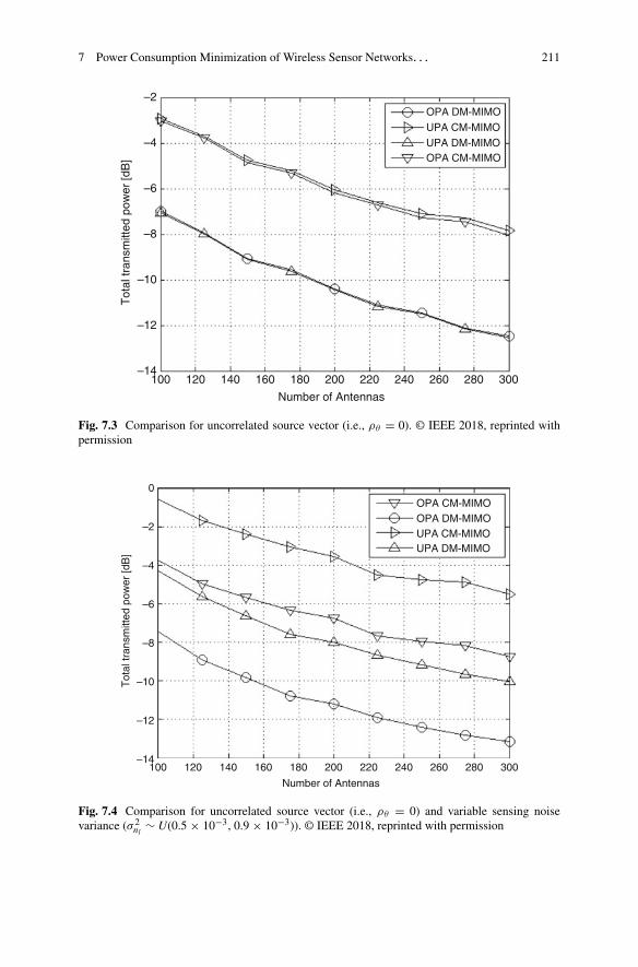
7 Power Consumption Minimization of Wireless Sensor Networks. . . 211
Tot
al tr
ansm
itted
pow
er [d
B]
–12
–10
–8
–6
–4
–2
–14100 120 140 160 180
Number of Antennas
OPA DM-MIMO
OPA CM-MIMO
UPA CM-MIMO
UPA DM-MIMO
220 240200 260 300280
Fig. 7.3 Comparison for uncorrelated source vector (i.e., ρθ = 0). © IEEE 2018, reprinted withpermission
Tot
al tr
ansm
itted
pow
er [d
B]
–12
–10
–8
–6
–4
–2
0
–14100 120 140 160 180
Number of Antennas
OPA CM-MIMO
UPA DM-MIMO
OPA DM-MIMOUPA CM-MIMO
220 240200 260 300280
Fig. 7.4 Comparison for uncorrelated source vector (i.e., ρθ = 0) and variable sensing noisevariance (σ 2
nl∼ U(0.5 × 10⁻³, 0.9 × 10⁻³)). © IEEE 2018, reprinted with permission
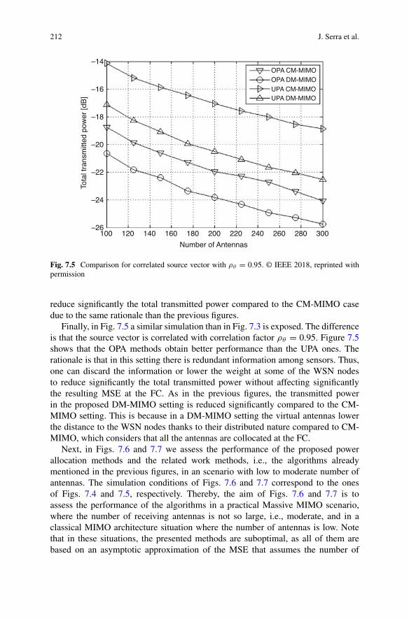
212 J. Serra et al.
Tota
l tra
nsm
itted
pow
er [d
B]
–24
–22
–20
–18
–16
–14
–26100 120 140 160 180
Number of Antennas
OPA CM-MIMO
UPA DM-MIMO
OPA DM-MIMOUPA CM-MIMO
220 240200 260 300280
Fig. 7.5 Comparison for correlated source vector with ρθ = 0.95. © IEEE 2018, reprinted withpermission
reduce significantly the total transmitted power compared to the CM-MIMO casedue to the same rationale than the previous figures.
Finally, in Fig. 7.5 a similar simulation than in Fig. 7.3 is exposed. The differenceis that the source vector is correlated with correlation factor ρθ = 0.95. Figure 7.5shows that the OPA methods obtain better performance than the UPA ones. Therationale is that in this setting there is redundant information among sensors. Thus,one can discard the information or lower the weight at some of the WSN nodesto reduce significantly the total transmitted power without affecting significantlythe resulting MSE at the FC. As in the previous figures, the transmitted powerin the proposed DM-MIMO setting is reduced significantly compared to the CM-MIMO setting. This is because in a DM-MIMO setting the virtual antennas lowerthe distance to the WSN nodes thanks to their distributed nature compared to CM-MIMO, which considers that all the antennas are collocated at the FC.
Next, in Figs. 7.6 and 7.7 we assess the performance of the proposed powerallocation methods and the related work methods, i.e., the algorithms alreadymentioned in the previous figures, in an scenario with low to moderate number ofantennas. The simulation conditions of Figs. 7.6 and 7.7 correspond to the onesof Figs. 7.4 and 7.5, respectively. Thereby, the aim of Figs. 7.6 and 7.7 is toassess the performance of the algorithms in a practical Massive MIMO scenario,where the number of receiving antennas is not so large, i.e., moderate, and in aclassical MIMO architecture situation where the number of antennas is low. Notethat in these situations, the presented methods are suboptimal, as all of them arebased on an asymptotic approximation of the MSE that assumes the number of
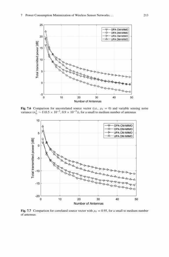
7 Power Consumption Minimization of Wireless Sensor Networks. . . 213
Fig. 7.6 Comparison for uncorrelated source vector (i.e., ρθ = 0) and variable sensing noisevariance (σ 2
nl∼ U(0.5 × 10⁻³, 0.9 × 10⁻³)), for a small to medium number of antennas
Fig. 7.7 Comparison for correlated source vector with ρθ = 0.95, for a small to medium numberof antennas
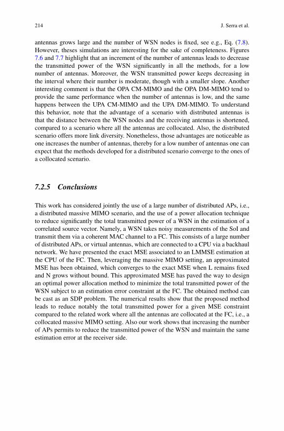
214 J. Serra et al.
antennas grows large and the number of WSN nodes is fixed, see e.g., Eq. (7.8).However, theses simulations are interesting for the sake of completeness. Figures7.6 and 7.7 highlight that an increment of the number of antennas leads to decreasethe transmitted power of the WSN significantly in all the methods, for a lownumber of antennas. Moreover, the WSN transmitted power keeps decreasing inthe interval where their number is moderate, though with a smaller slope. Anotherinteresting comment is that the OPA CM-MIMO and the OPA DM-MIMO tend toprovide the same performance when the number of antennas is low, and the samehappens between the UPA CM-MIMO and the UPA DM-MIMO. To understandthis behavior, note that the advantage of a scenario with distributed antennas isthat the distance between the WSN nodes and the receiving antennas is shortened,compared to a scenario where all the antennas are collocated. Also, the distributedscenario offers more link diversity. Nonetheless, those advantages are noticeable asone increases the number of antennas, thereby for a low number of antennas one canexpect that the methods developed for a distributed scenario converge to the ones ofa collocated scenario.
7.2.5 Conclusions
This work has considered jointly the use of a large number of distributed APs, i.e.,a distributed massive MIMO scenario, and the use of a power allocation techniqueto reduce significantly the total transmitted power of a WSN in the estimation of acorrelated source vector. Namely, a WSN takes noisy measurements of the SoI andtransmit them via a coherent MAC channel to a FC. This consists of a large numberof distributed APs, or virtual antennas, which are connected to a CPU via a backhaulnetwork. We have presented the exact MSE associated to an LMMSE estimation atthe CPU of the FC. Then, leveraging the massive MIMO setting, an approximatedMSE has been obtained, which converges to the exact MSE when L remains fixedand N grows without bound. This approximated MSE has paved the way to designan optimal power allocation method to minimize the total transmitted power of theWSN subject to an estimation error constraint at the FC. The obtained method canbe cast as an SDP problem. The numerical results show that the proposed methodleads to reduce notably the total transmitted power for a given MSE constraintcompared to the related work where all the antennas are collocated at the FC, i.e., acollocated massive MIMO setting. Also our work shows that increasing the numberof APs permits to reduce the transmitted power of the WSN and maintain the sameestimation error at the receiver side.
7 Power Consumption Minimization of Wireless Sensor Networks. . . 215
7.3 Harvesting Artificial Light Indoors to Power Perpetuallya WSN Node
7.3.1 Introduction
EH systems capture energy from different environmental sources. A variety of EHsources exist depending on the scenario and the application, e.g., light, motion,vibration, wind, heat, or electromagnetic waves [14]. Moreover, EH systemstransform the harvested energy into electrical energy and store it in a battery. Apower management subsystem, within the EH module, defines a proper electricalinterface to power a WSN device with the harvested energy. Thereby, EH is thecornerstone to extend the WSN devices’ lifetime. This work investigates EH forindoors and, in particular, we focus on EH from artificial light. EH in indoorenvironments is a challenging scenario since the average power that can be harvestedfrom ambient light, is 10 to 100 times lower than in outdoor environments [15].
Several works deal with EH from ambient light in the literature. In [15], a hybridEH module is proposed, which gathers energy from both ambient and thermallight. They propose a single power management unit for both sources of energy.The authors in [16] characterize the indoors light energy availability and theydevelop energy allocation algorithms for EH devices. The work in [17] considersWSN devices that harvest ambient light energy, both from solar and artificial lightsources. Each WSN device is equipped with presence and light sensors, and theirmeasurements are used by a central controller to adapt the illumination of the indoorlight system. In [18], the authors characterize the indoor light conditions not only interms of light intensity, but also in terms of its spectral information. This leads to aprecise estimation of the output power that a photovoltaic panel can obtain from thegiven ambient light conditions.
Herein we demonstrate experimentally energy neutrality in WSN devices basedon energy harvested from artificial light. The proposed solution consists of an EHmodule that powers a WSN source node which is transmitting data to a WSN sinknode. The EH module consists of a PV cell that harvests artificial light from a nearbylamp, a boost converter that transforms the gathered energy into the proper electricalfeatures of the WSN node and a 3 V rechargeable coin-type battery that stores theelectrical energy.
7.3.2 Related Work
Several related works have been presented in the literature though some of themfocus on harvesting solar light in outdoor scenarios. In [19], the authors presenta low cost solar harvesting system constituted by WSN MICAz nodes and theMAX1724EZK33 boost converter, by Maxim Integrated, which achieves a per-petual power supply. Unlike in [19], this work focuses in an indoor environment.
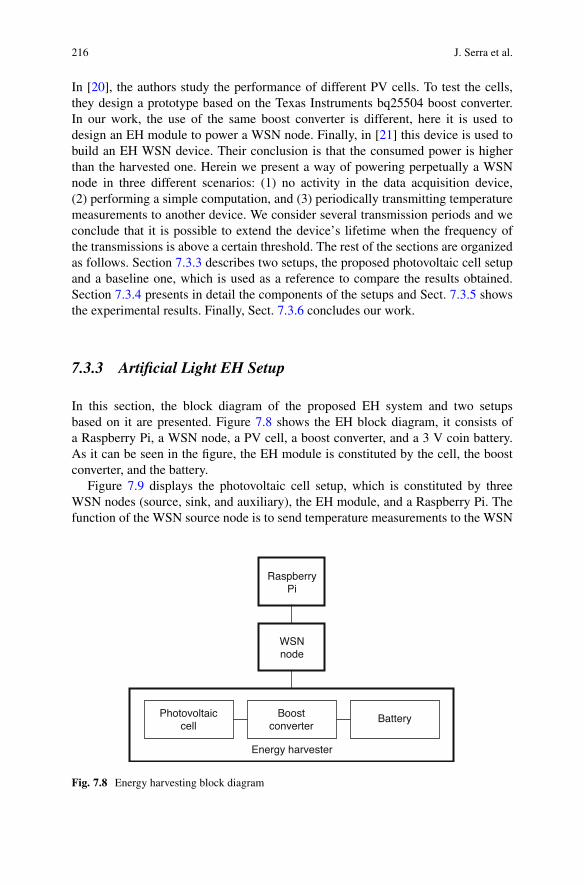
216 J. Serra et al.
In [20], the authors study the performance of different PV cells. To test the cells,they design a prototype based on the Texas Instruments bq25504 boost converter.In our work, the use of the same boost converter is different, here it is used todesign an EH module to power a WSN node. Finally, in [21] this device is used tobuild an EH WSN device. Their conclusion is that the consumed power is higherthan the harvested one. Herein we present a way of powering perpetually a WSNnode in three different scenarios: (1) no activity in the data acquisition device,(2) performing a simple computation, and (3) periodically transmitting temperaturemeasurements to another device. We consider several transmission periods and weconclude that it is possible to extend the device’s lifetime when the frequency ofthe transmissions is above a certain threshold. The rest of the sections are organizedas follows. Section 7.3.3 describes two setups, the proposed photovoltaic cell setupand a baseline one, which is used as a reference to compare the results obtained.Section 7.3.4 presents in detail the components of the setups and Sect. 7.3.5 showsthe experimental results. Finally, Sect. 7.3.6 concludes our work.
7.3.3 Artificial Light EH Setup
In this section, the block diagram of the proposed EH system and two setupsbased on it are presented. Figure 7.8 shows the EH block diagram, it consists ofa Raspberry Pi, a WSN node, a PV cell, a boost converter, and a 3 V coin battery.As it can be seen in the figure, the EH module is constituted by the cell, the boostconverter, and the battery.
Figure 7.9 displays the photovoltaic cell setup, which is constituted by threeWSN nodes (source, sink, and auxiliary), the EH module, and a Raspberry Pi. Thefunction of the WSN source node is to send temperature measurements to the WSN
Photovoltaiccell
Boostconverter
Battery
RaspberryPi
WSNnode
Energy harvester
Fig. 7.8 Energy harvesting block diagram
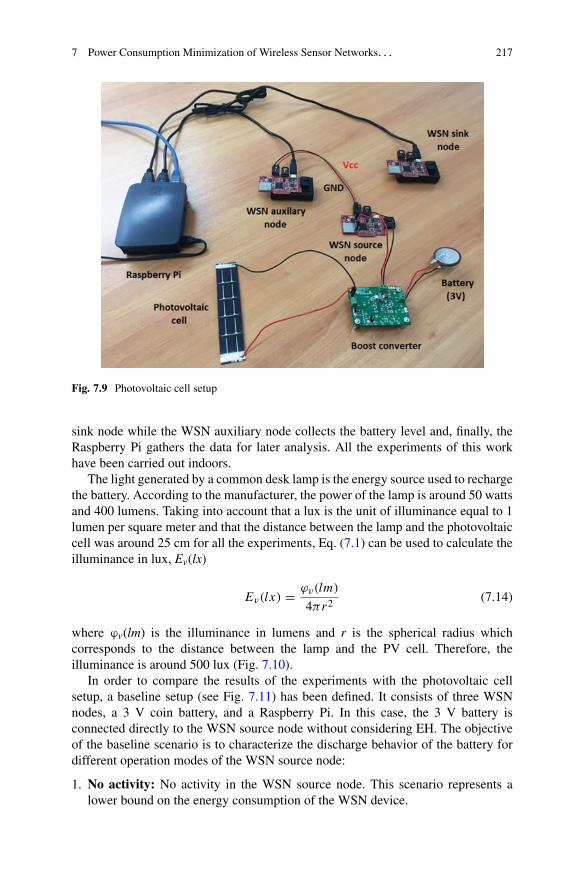
7 Power Consumption Minimization of Wireless Sensor Networks. . . 217
Fig. 7.9 Photovoltaic cell setup
sink node while the WSN auxiliary node collects the battery level and, finally, theRaspberry Pi gathers the data for later analysis. All the experiments of this workhave been carried out indoors.
The light generated by a common desk lamp is the energy source used to rechargethe battery. According to the manufacturer, the power of the lamp is around 50 wattsand 400 lumens. Taking into account that a lux is the unit of illuminance equal to 1lumen per square meter and that the distance between the lamp and the photovoltaiccell was around 25 cm for all the experiments, Eq. (7.1) can be used to calculate theilluminance in lux, Ev(lx)
Ev(lx) = ϕv(lm)
4πr2 (7.14)
where ϕv(lm) is the illuminance in lumens and r is the spherical radius whichcorresponds to the distance between the lamp and the PV cell. Therefore, theilluminance is around 500 lux (Fig. 7.10).
In order to compare the results of the experiments with the photovoltaic cellsetup, a baseline setup (see Fig. 7.11) has been defined. It consists of three WSNnodes, a 3 V coin battery, and a Raspberry Pi. In this case, the 3 V battery isconnected directly to the WSN source node without considering EH. The objectiveof the baseline scenario is to characterize the discharge behavior of the battery fordifferent operation modes of the WSN source node:
1. No activity: No activity in the WSN source node. This scenario represents alower bound on the energy consumption of the WSN device.
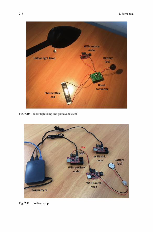
218 J. Serra et al.
Fig. 7.10 Indoor light lamp and photovoltaic cell
Fig. 7.11 Baseline setup
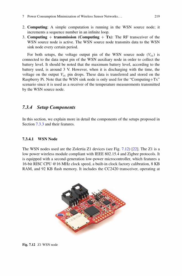
7 Power Consumption Minimization of Wireless Sensor Networks. . . 219
2. Computing: A simple computation is running in the WSN source node; itincrements a sequence number in an infinite loop.
3. Computing + transmission (Computing + Tx): The RF transceiver of theWSN source node is active. The WSN source node transmits data to the WSNsink node every certain period.
For both setups, the voltage output pin of the WSN source node (Vcc) isconnected to the data input pin of the WSN auxiliary node in order to collect thebattery level. It should be noted that the maximum battery level, according to thebattery used, is around 3 V. However, when it is discharging with the time, thevoltage on the output Vcc pin drops. These data is transferred and stored on theRaspberry Pi. Note that the WSN sink node is only used for the “Computing+Tx”scenario since it is used as a receiver of the temperature measurements transmittedby the WSN source node.
7.3.4 Setup Components
In this section, we explain more in detail the components of the setups proposed inSection 7.3.3 and their features.
7.3.4.1 WSN Node
The WSN nodes used are the Zolertia Z1 devices (see Fig. 7.12) [22]. The Z1 is alow power wireless module compliant with IEEE 802.15.4 and Zigbee protocols. Itis equipped with a second-generation low-power microcontroller, which features a16-bit RISC CPU @16 MHz clock speed, a built-in clock factory calibration, 8 KBRAM, and 92 KB flash memory. It includes the CC2420 transceiver, operating at
Fig. 7.12 Z1 WSN node

220 J. Serra et al.
2.4 GHz frequency band with a data rate of 250 Kbps. It supports Contiki OS, anopen-source operating system for the IoT, which connects tiny, low-cost, low-powermicrocontrollers to the Internet. Each Z1 device can operate as either a source ora sink node. According to [22], the consumption in transmission mode is around17.4 mA for a transmission power of 0 dBm, 18.8 mA in reception mode, lessthan 10 mA when the microcontroller is active and the consumption of the memorycircuit is up to 15 mA. The Z1 can be powered with two AA batteries (1.5 V eachone). However, in this work the EH module has been used to power the device.
7.3.4.2 Raspberry Pi 3
Figure 7.13 shows a Raspberry Pi 3, which is a single-board computer withwireless LAN and Bluetooth connectivity. It is equipped with a Quad Core 1.2 GHzBroadcom BCM2837 64 bit CPU and 1 GB RAM. Its role is mainly to gather datafrom the WSN source node’s lifetime for the different scenarios and setups.
7.3.4.3 Rechargeable Coin Batteries
Two 3 V coin-type rechargeable lithium batteries of 50 mAh (VL2330) and100 mAh (VL3032) capacity have been chosen, they are provided by Panasonic[23] (see Fig. 7.14). Although there are smaller capacity batteries in the market,they are not considered because they cannot assume the power consumption of theWSN node and the boost converter.
7.3.4.4 Boost Converter
Figure 7.15 shows the boost converter used for the photovoltaic cell setup; itis the bq25504 evaluation module by Texas Instruments. According to [24], the
Fig. 7.13 Raspberry Pi 3 Model B
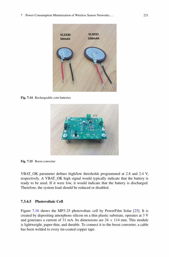
7 Power Consumption Minimization of Wireless Sensor Networks. . . 221
Fig. 7.14 Rechargeable coin batteries
Fig. 7.15 Boost converter
VBAT_OK parameter defines high/low thresholds programmed at 2.8 and 2.4 V,respectively. A VBAT_OK high signal would typically indicate that the battery isready to be used. If it were low, it would indicate that the battery is discharged.Therefore, the system load should be reduced or disabled.
7.3.4.5 Photovoltaic Cell
Figure 7.16 shows the MP3-25 photovoltaic cell by PowerFilm Solar [25]. It iscreated by depositing amorphous silicon on a thin plastic substrate, operates at 3 Vand generates a current of 31 mA. Its dimensions are 24 × 114 mm. This moduleis lightweight, paper-thin, and durable. To connect it to the boost converter, a cablehas been welded to every tin-coated copper tape.

222 J. Serra et al.
Fig. 7.16 Photovoltaic cell
7.3.5 Experimental Results
This section is structured in two subsections. The first subsection considers thebaseline setup and shows the performance of both 50 and 100 mAh capacitybatteries. The objective of these experiments is to evaluate both batteries and decidewhether the 50 mAh capacity battery is enough to achieve a perpetual power supplyof the source WSN node or the 100 mAh capacity battery is needed. Then, oncedecided the most appropriate battery, the second set of experiments demonstrateshow we achieve the goal of this work, evaluating the battery for the differentscenarios described in Sect. 7.3.3.
7.3.5.1 Baseline Setup Experiments
These experiments have been performed using the baseline setup described in Sect.7.3.3 (see Fig. 7.11). The objective here is to study the behavior of the batterieswithout considering the EH module; therefore, connecting directly the battery to theWSN source node. The operating range of the WSN device microcontroller rangesfrom 1.8 to 3.6 V, this means that below 1.8 V the WSN source node may not workproperly.
Figures 7.17 and 7.18 shows the baseline results for the 50 and 100 mAhcapacity battery for “No activity,” “Computing,” and “Computing + Tx” (with atransmission period of 5 s) scenarios. As it can be seen if the activity in the WSNsource node increases, the operating time of the battery decreases. Namely, thepower consumption due to the communication resources and computational usageis greater in the “Computing+Tx” scenario than in the “Computing” one and thesame happens in the “Computing” scenario compared to the “No activity” one. Infact, Fig. 7.17 shows the performance of the 50mAh battery, it can be appreciated
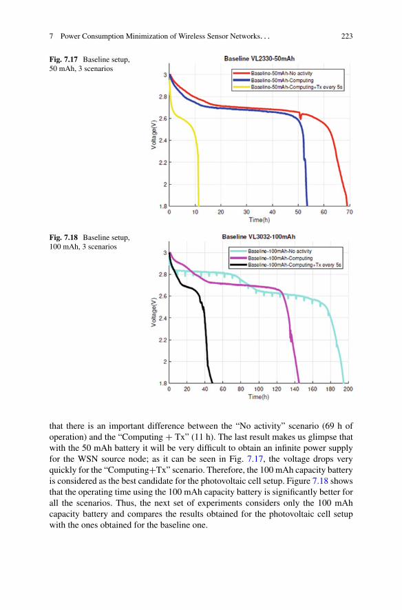
7 Power Consumption Minimization of Wireless Sensor Networks. . . 223
Fig. 7.17 Baseline setup,50 mAh, 3 scenarios
Fig. 7.18 Baseline setup,100 mAh, 3 scenarios
that there is an important difference between the “No activity” scenario (69 h ofoperation) and the “Computing + Tx” (11 h). The last result makes us glimpse thatwith the 50 mAh battery it will be very difficult to obtain an infinite power supplyfor the WSN source node; as it can be seen in Fig. 7.17, the voltage drops veryquickly for the “Computing+Tx” scenario. Therefore, the 100 mAh capacity batteryis considered as the best candidate for the photovoltaic cell setup. Figure 7.18 showsthat the operating time using the 100 mAh capacity battery is significantly better forall the scenarios. Thus, the next set of experiments considers only the 100 mAhcapacity battery and compares the results obtained for the photovoltaic cell setupwith the ones obtained for the baseline one.
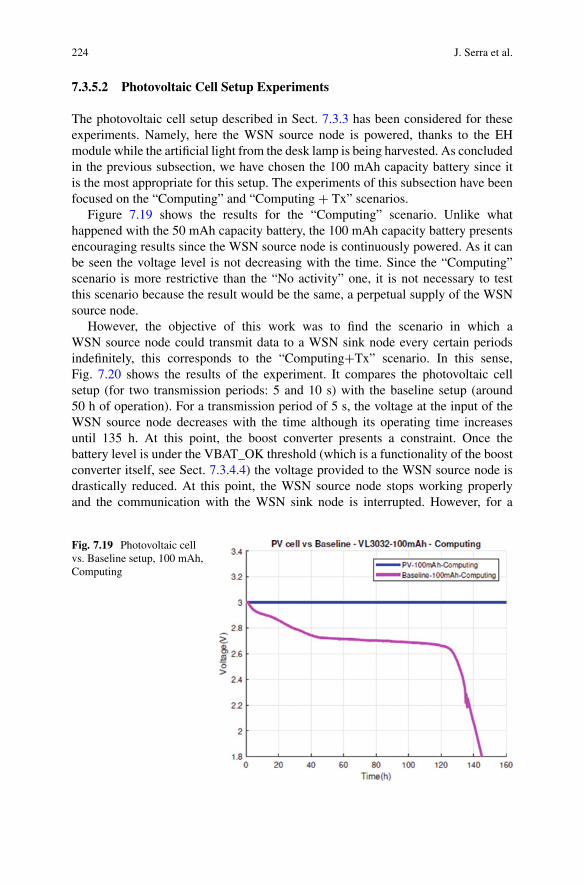
224 J. Serra et al.
7.3.5.2 Photovoltaic Cell Setup Experiments
The photovoltaic cell setup described in Sect. 7.3.3 has been considered for theseexperiments. Namely, here the WSN source node is powered, thanks to the EHmodule while the artificial light from the desk lamp is being harvested. As concludedin the previous subsection, we have chosen the 100 mAh capacity battery since itis the most appropriate for this setup. The experiments of this subsection have beenfocused on the “Computing” and “Computing + Tx” scenarios.
Figure 7.19 shows the results for the “Computing” scenario. Unlike whathappened with the 50 mAh capacity battery, the 100 mAh capacity battery presentsencouraging results since the WSN source node is continuously powered. As it canbe seen the voltage level is not decreasing with the time. Since the “Computing”scenario is more restrictive than the “No activity” one, it is not necessary to testthis scenario because the result would be the same, a perpetual supply of the WSNsource node.
However, the objective of this work was to find the scenario in which aWSN source node could transmit data to a WSN sink node every certain periodsindefinitely, this corresponds to the “Computing+Tx” scenario. In this sense,Fig. 7.20 shows the results of the experiment. It compares the photovoltaic cellsetup (for two transmission periods: 5 and 10 s) with the baseline setup (around50 h of operation). For a transmission period of 5 s, the voltage at the input of theWSN source node decreases with the time although its operating time increasesuntil 135 h. At this point, the boost converter presents a constraint. Once thebattery level is under the VBAT_OK threshold (which is a functionality of the boostconverter itself, see Sect. 7.3.4.4) the voltage provided to the WSN source node isdrastically reduced. At this point, the WSN source node stops working properlyand the communication with the WSN sink node is interrupted. However, for a
Fig. 7.19 Photovoltaic cellvs. Baseline setup, 100 mAh,Computing
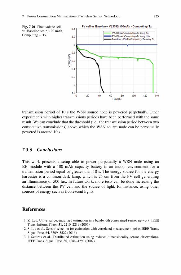
7 Power Consumption Minimization of Wireless Sensor Networks. . . 225
Fig. 7.20 Photovoltaic cellvs. Baseline setup, 100 mAh,Computing + Tx
transmission period of 10 s the WSN source node is powered perpetually. Otherexperiments with higher transmissions periods have been performed with the sameresult. We can conclude that the threshold (i.e., the transmission period between twoconsecutive transmissions) above which the WSN source node can be perpetuallypowered is around 10 s.
7.3.6 Conclusions
This work presents a setup able to power perpetually a WSN node using anEH module with a 100 mAh capacity battery in an indoor environment for atransmission period equal or greater than 10 s. The energy source for the energyharvester is a common desk lamp, which is 25 cm from the PV cell generatingan illuminance of 500 lux. In future work, more tests can be done increasing thedistance between the PV cell and the source of light, for instance, using othersources of energy such as fluorescent lights.
References
1. Z. Luo, Universal decentralized estimation in a bandwidth constrained sensor network. IEEETrans. Inform. Theor. 51, 2210–2219 (2005)
2. S. Liu et al., Sensor selection for estimation with correlated measurement noise. IEEE Trans.Signal Proc. 64, 3509–3522 (2016)
3. I. Schizas et al., Distributed estimation using reduced-dimensionality sensor observations.IEEE Trans. Signal Proc. 55, 4284–4299 (2007)

226 J. Serra et al.
4. A. Shirazinia, S. Dey, Power-constrained sparse gaussian linear dimensionality reduction overnoisy channels. IEEE Trans. Signal Proc. 63, 5837–5852 (2015)
5. A. Behbahani, A. Eltawil, H. Jafarkhani, Decentralized estimation under correlated noise. IEEETrans. Signal Proc. 62, 5603–5614 (2014)
6. E. Bjronson et al., Deploying dense networks for maximal energy efficiency: Smmall cellsmeet massive MIMO. IEEE J. Select. Areas Commun. 34, 832–847 (2016)
7. M. Kamel, W. Hamouda, A. Youssef, Ultra-dense networks: A survey. IEEE Commun. Surv.Tutor. 18, 2522–2545., Fourth quarter (2016)
8. T. Marzetta, Noncooperative cellular wireless with unlimited numbers of base station antennas.IEEE Trans. Wirel. Commun. 9, 3590–3600 (2010)
9. F. Jiang, J. Chen, A. Swindlehurst, Phase-only analog encoding for a multi-antenna fusioncenter, in Proc. IEEE ICASSP, (2012), pp. 2645–2648
10. A. Swindlehurst et al., Massive MIMO for wireless sensing with a coherent multiple accesschannel. IEEE Trans. Signal Proc. 63, 3005–3017 (2015)
11. A. Shirazinia et al., Massive MIMO for decentralized estimation of a correlated source. IEEETrans. Signal Proc. 64, 2499–2512 (2016)
12. T.L. Marzetta et al., Cell-free massive MIMO versus small cells. IEEE Trans. Wirel. Commun.16, 1834–1850 (2017)
13. S. Kay, Fundamentals of Statistical Signal Processing: Estimation Theory (Prentice-Hall,Upper Saddle River, NJ, 1993)
14. O. Cetinkaya, O. Akan, Electric-field energy harvesting from lighting elements for battery-lessinternet of things. IEEE Access 5, 7423–7434 (2017)
15. Y. Tan, S. Panda, Energy harvesting from hybrid indoor ambient light and thermal energysources for enhanced performance of wireless sensor nodes. IEEE Trans. Indus. Electr. 58,4424–4435 (2011)
16. M. Gorlatova et al., Networking low-power energy harvesting devices: Measurements andalgorithms. IEEE Trans. Mob. Comput. 12, 1853–1865 (2013)
17. S. Li, A. Pandharipande, Networked illumination control with distributed light-harvestingwireless sensors. IEEE Sens. J. 15, 1662–1669 (2015)
18. X. Ma, S. Bader, B. Oelmann, Characterization of indoor light conditions by light sourceclassification. IEEE Sens. J. 17, 3884–3891 (2017)
19. L.J. Chien et al., A simple solar energy harvester for wireless sensor networks, in 6thInternational Conference on Intelligent and Advanced Systems (ICIAS), (2016), pp. 1–6
20. M. Rasheduzzaman et al., A study of the performance of solar cells for indoor autonomouswireless sensors, in 10th International Symposium on Communication Systems, Networks andDigital Signal Processing (CSNDSP), (2016), pp. 1–6
21. A.E. Xhafa et al., Towards a perpetual wireless sensor node. IEEE Sens. J., 1–4 (2013)22. “Z1 datasheet, Zolertia.” http://zolertia.sourceforge.net/wiki/images/e/e8/
Z1_RevC_Datasheet.pdf23. “Coin type rechargeable lithium batteries (VL series), Panasonic.” https://
industrial.panasonic.com/ww/products/batteries/primary-batteries/lithium-batteries/coin-type-rechargeable-lithium-batteries-vl-series?reset=1
24. “bq25504 EVM—Ultra Low Power Boost Converter with Battery Management for EnergyHarvester Applications, Texas Instruments.” http://www.ti.com/lit/ug/sluu654a/sluu654a.pdf
25. “MP3–25 Photovoltaic cell, PowerFilm.” http://www.powerfilmsolar.com/products/?&show=product&productID=271534&productCategoryIDs=6573
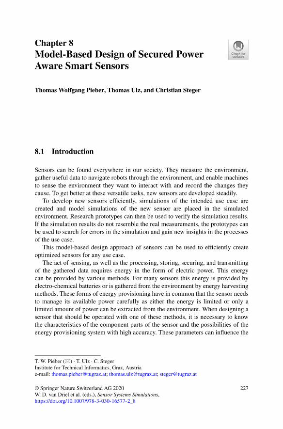
Chapter 8Model-Based Design of Secured PowerAware Smart Sensors
Thomas Wolfgang Pieber, Thomas Ulz, and Christian Steger
8.1 Introduction
Sensors can be found everywhere in our society. They measure the environment,gather useful data to navigate robots through the environment, and enable machinesto sense the environment they want to interact with and record the changes theycause. To get better at these versatile tasks, new sensors are developed steadily.
To develop new sensors efficiently, simulations of the intended use case arecreated and model simulations of the new sensor are placed in the simulatedenvironment. Research prototypes can then be used to verify the simulation results.If the simulation results do not resemble the real measurements, the prototypes canbe used to search for errors in the simulation and gain new insights in the processesof the use case.
This model-based design approach of sensors can be used to efficiently createoptimized sensors for any use case.
The act of sensing, as well as the processing, storing, securing, and transmittingof the gathered data requires energy in the form of electric power. This energycan be provided by various methods. For many sensors this energy is provided byelectro-chemical batteries or is gathered from the environment by energy harvestingmethods. These forms of energy provisioning have in common that the sensor needsto manage its available power carefully as either the energy is limited or only alimited amount of power can be extracted from the environment. When designing asensor that should be operated with one of these methods, it is necessary to knowthe characteristics of the component parts of the sensor and the possibilities of theenergy provisioning system with high accuracy. These parameters can influence the
T. W. Pieber (�) · T. Ulz · C. StegerInstitute for Technical Informatics, Graz, Austriae-mail: [email protected]; [email protected]; [email protected]
© Springer Nature Switzerland AG 2020W. D. van Driel et al. (eds.), Sensor Systems Simulations,https://doi.org/10.1007/978-3-030-16577-2_8
227
228 T. W. Pieber et al.
design of the sensor massively. That means that the components of the sensor need tomatch the requirements for the intended use case and the energy provisioning needsto be capable of providing sufficient energy to operate the sensor for the intendedlifetime and operations. To work efficiently the sensor has to be aware of its powerusage and the current capabilities of the energy provisioning system.
The data that is generated by the sensors is mostly seen as not harmful to theprocess they monitor. This can be seen as the most common approach to datasecurity of sensor data is “What can be measured can be seen by anyone”. Thisnotion of data security is now seen as a fallacy as the STUXNET [9] and HAVEX[4] attacks have been noted. Furthermore, as the Mirai botnet [2] shows, unsecuredsensors also pose a threat to other targets. To circumvent these threats, measures tosecure the system and the generated data need to be taken.
To prevent the new sensor to be exploited in such way, the security of the systemand data is of utmost importance, and thus, must not be neglected during the designof the new sensor system.
The paragraphs above describe a sensor that can not only generate data about theenvironment, but also about itself and take informed decisions. It can furthermoremodify the data and perform security relevant operations on it. Beyond that, it canreceive and send such data to form a network. It also knows its current powerstatus and can perform actions to prolong its lifetime or let the network know ifthe remaining energy gets too low.
Such a sensor that is able to perform informed measures on itself, the data, or thenetwork can be called a smart sensor.
This chapter follows the design process shown in Fig. 8.1.
Fig. 8.1 Concept of a model based design process for a secured power aware smart sensor
8 Model-Based Design of Secured Power Aware Smart Sensors 229
• A reference system is created that shows all processes we want to model.• The reference system is measured to understand the processes.• A simulation of the system is created to abstract the system.• The use case is modelled and simulated.• The simulation of the new system is connected to the simulation of the use case.• The results of the simulations are evaluated. If the results are not as expected, the
process is restarted.
In this chapter we use this design approach to create a sensor that is read andcharged by using NFC technology. To do so autonomous robots in an Industry 4.0inspired setting will communicate to the sensors and connect them to a network.
8.2 Related Publications
Simulation BackgroundThe use of simulation to predict sensor functionality and the methods to get theparameters of the sensor components have been described in many publications.
In this publication we want to use the robotic simulation tool Gazebo [14] as acore system. The connection of a Matlab environment to Gazebo has been publishedon the official website [12]. This tutorial shows how to connect Matlab to Gazebovia the ROS (Robot Operating System) interface to send and receive data from theGazebo simulation.
Further publications connect the Gazebo simulator with different software formachine learning [26]. Also here the software is connecting to the operating systemcontrolling the robot and influences the path the robot takes to reach a goal.
SystemC [1] is a hardware description language based on C++. It is capable ofdescribing the hardware on different levels of abstraction. This is especially usefulas a detailed description of all components results in a very slow, albeit accurate,simulation. This is furthermore useful if developing a simulation from scratch as thecomponents can be described in an abstract way and be defined in later steps. Thepublication of Panda shows design processes to create SystemC simulations [15].
The connection of SystemC to different simulation tools has been describedin many publications [3, 7, 11, 13, 18]. In these works the SystemC simulation isprimarily used as a kernel to provide the functionality of the quasi parallel execution.
The connection of SystemC to Matlab was designed by Bouchhima et al. [3] AsMatlab works with discrete events, they created this cosimulation to additionallysimulate continuous events.
To speed up the SystemC simulations, Huang et al. [7] describe a possibility tospread the simulation across a network of computers.
SystemC can also be connected to a simulation tool designed for integratedcircuit simulation [11]. Martin et al. connected it to a SPICE (Simulation Programwith Integrated Circuit Emphasis) simulator as well as to a VHDL (Very high speedintegrated circuit Hardware Description Language) simulation.

230 T. W. Pieber et al.
Mueller-Gritschneder et al. [13] used SystemC to compute physical processesthat affect the robot while it is moving. This simulation therefore generates data inthe SystemC simulation that is then used to model the robots behaviour. In contrastto that, our approach generates data in the environment and uses this as input forthe SystemC simulation.
Pieber et al. [16] describe methods to connect a SystemC simulation to theGazebo environment in one of their publications. This paper describes in detailhow the connection between the simulations can be formed and what requirementsneed to be fulfilled to create a successful simulation. This publication furthermoreannounces possible advancements to increase the simulation speed if multipleSystemC simulations need to be run at the same time.
Power Awareness for SensorsThe idea that sensors are aware of their own power levels and power consumptionhas been discussed in many publications [5, 8, 10, 19, 20, 25]. Using this informa-tion, the sensors can make decisions about the routing of information inside thenetwork, reduce the quality of the measurements to prolong the lifetime, or informthe network that the energy level is too low to actively take part in the task of thenetwork.
Chen et al. [5] developed a small energy harvesting sensor node that is capable ofproviding its own energy. This sensor node relies on solar cells to charge a battery. Ifthe charge in the battery is sufficient, the sensor wakes and performs its operationsuntil the voltage drops below a predefined value. Then the sensor switches to aultra-low power sleep mode. In this scenario the sensors duty cycle is provided bythe capabilities of the energy harvesting system.
To calculate a duty cycle for a energy harvesting sensor system the energyusage and harvesting capabilities must be known. Kansal et al. [8] formalizedthese calculations in their work. These configurations can be used to initializesuch system. If the observed parameters at the position of the sensor differ fromthe predicted ones, the team of researchers propose a dynamically changing dutycycle. Using this dynamically changing system the researchers noted a significantlyimproved performance of their research system.
Additionally Rahimi et al. [19] explore the possibility to expand the sensorslifetime using energy harvesting methods. In their research they try to exploitautonomously moving nodes. These nodes search in a so-called Energy Cell forthe optimal spot to harvest solar energy. Afterwards the moving nodes provide thisenergy to the sensor nodes in their assigned cell.
Another possible energy source that can be used by the sensor nodes is RF energyfrom broadcasting stations. Sogorb et al. [20] use sensor nodes with two antennas toresearch this possibility. In their research prototype one antenna is used to harvestthe energy from broadcasting stations, the other one to transmit the gathered data toa base station.
Another strategy that uses RF energy harvesting has been explored by Leeet al. [10]. This research team focused on the possibility to harvest energy usingantiparallel resonant loops. The researchers explore RFID’s (Radio Frequency
8 Model-Based Design of Secured Power Aware Smart Sensors 231
IDentification) capability to transmit energy. They stated that antiparallel loops canimprove the efficiency of energy transmission to 87% from about 50%.
The researchers around Yan [25] explored methods to construct more efficientsensor networks. This is done by making the sensors aware of their own energystate. In this research Yan et al. implemented two levels of energy saving. “Node-level energy saving” adaptively regulates the transmission power of the sensornode. “Network-level energy saving” adaptively reconfigures the sensor networksconfiguration.
Security for SensorsSecurity for sensor devices has been researched in the literature [6, 17, 22–24]. Mostresearchers however see security as a side topic to be added later to an existingsensor hardware.
The work by Ulz et al. [24] describes multiple methods how sensor data canbe secured. The researchers pointed towards problems that arise if sensor datais encrypted and how these problems can be mitigated. In their publication theresearchers use authenticated encryption (AE) to securely transmit data betweena sensor of a control system and the controller. The researchers state that using onlythis technique a DoS attack is easier to perform. To counteract this problem forwarderror correction techniques have been proposed. Furthermore, the researchers statethat a security controller can be used to perform these operations as this processingunit is specialized to perform the task of encrypting more efficiently than a regularmicrocontroller.
In addition to securing the data of a sensor against adversaries Ulz et al. [22]proposed methods to secure a sensor network against misuse and misconfiguredsensors using a security controller. This paper presents the idea of a two-layerattestation system that first checks the validity of a sensors firmware, and in a secondstep validates the version of this firmware. Another publication by this researchersdescribes an update mechanism for such sensor system [23]. Here the researchersstate that the interface to update the sensor needs to be separated of the maincommunication interface.
To prevent the misuse of single sensors, authentication to see and modifydata is necessary. Pieber et al. [17] describe a method to use a password-basedauthentication method that is lightweight enough to be run on a single sensor.
Haase et al. [6] propose a system to (re-)configure a sensor system via NFC. Theyfurthermore use cryptography to authenticate the reconfiguration device.
8.3 Obtaining Data for the Models
To get a decent simulation of any system, the processes and components of thesystem need to be understood. A smart sensor consists at least of the followingparts:
• The sensor frontend: The part of the sensor that does the conversion from anexternal stimulus to digital information.

232 T. W. Pieber et al.
• The controller.• The memory.• A communication interface.• The energy provisioning system.• (Optional) A security controller to perform security relevant operations.
For these components data sheets are available that specify the peak current atan optimal voltage source. This is sufficient information to build the sensor, asoverestimation of the components energy usage leads to a more powerful energyprovisioning system. To get a better estimation of the energy demands of thesystem, and therefore be able to design a more optimal energy provisioning system,measurements have to be performed. This requires the development of a researchprototype.
To create an efficient sensor, a model of the environment and the intendeduse case is useful. Such simulation need not be very detailed as this allows thesimulation to be used in various ways and thus create a multitude of different stimulifor the sensor. The simulation of the environment needs at least these components:
• A representation of the new sensor.• Objects influencing the sensor or the communication with the sensor.• Communication partners for the smart sensor to test the used communication
protocols.• Things for the sensor to measure.
8.3.1 Measuring Data for the New Sensor
The prototype that is used to measure the sensor components should be able to varythe input voltages to emulate the energy provisioning system. This concept is shownin Fig. 8.2. Here a control program gets the values of the current consumption ofthe components and calculates how the voltage of the energy provisioning systemreacts to this current flow. The updated settings are transmitted to the testbenchwhere the voltage is generated. The smart sensor can now be operated with thisupdated voltage and the current flow changes. To have an optimal measurementof the drawn current a gain control unit can be used to set the sensor gains of thecurrent measurement units. The measured values are given to the control program tobe stored and to calculate the new settings for the testbench. The data gained fromthe measurements are used to construct models of the sensor components.
The data that is generated can then be used to create models of the sensorcomponents energy usage at different voltages. This data can furthermore be usedto specify the requirements for the energy provisioning system of the final sensor.
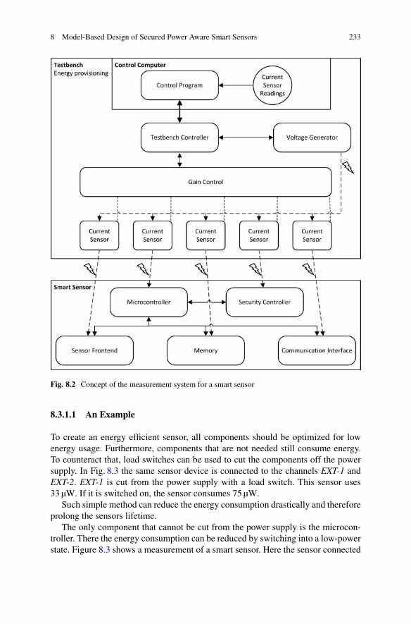
8 Model-Based Design of Secured Power Aware Smart Sensors 233
Fig. 8.2 Concept of the measurement system for a smart sensor
8.3.1.1 An Example
To create an energy efficient sensor, all components should be optimized for lowenergy usage. Furthermore, components that are not needed still consume energy.To counteract that, load switches can be used to cut the components off the powersupply. In Fig. 8.3 the same sensor device is connected to the channels EXT-1 andEXT-2. EXT-1 is cut from the power supply with a load switch. This sensor uses33 µW. If it is switched on, the sensor consumes 75 µW.
Such simple method can reduce the energy consumption drastically and thereforeprolong the sensors lifetime.
The only component that cannot be cut from the power supply is the microcon-troller. There the energy consumption can be reduced by switching into a low-powerstate. Figure 8.3 shows a measurement of a smart sensor. Here the sensor connected
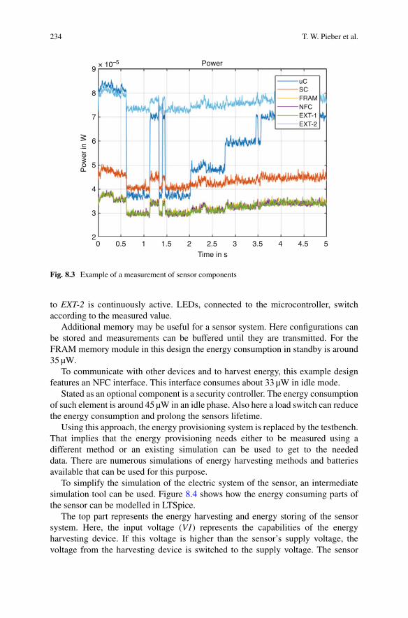
234 T. W. Pieber et al.
9
8
7
6
Pow
er in
W
5
4
3
20 0.5 1 1.5 2 2.5
Power
uCSCFRAMNFCEXT-1EXT-2
× 10–5
Time in s
3 3.5 4 4.5 5
Fig. 8.3 Example of a measurement of sensor components
to EXT-2 is continuously active. LEDs, connected to the microcontroller, switchaccording to the measured value.
Additional memory may be useful for a sensor system. Here configurations canbe stored and measurements can be buffered until they are transmitted. For theFRAM memory module in this design the energy consumption in standby is around35 µW.
To communicate with other devices and to harvest energy, this example designfeatures an NFC interface. This interface consumes about 33 µW in idle mode.
Stated as an optional component is a security controller. The energy consumptionof such element is around 45 µW in an idle phase. Also here a load switch can reducethe energy consumption and prolong the sensors lifetime.
Using this approach, the energy provisioning system is replaced by the testbench.That implies that the energy provisioning needs either to be measured using adifferent method or an existing simulation can be used to get to the neededdata. There are numerous simulations of energy harvesting methods and batteriesavailable that can be used for this purpose.
To simplify the simulation of the electric system of the sensor, an intermediatesimulation tool can be used. Figure 8.4 shows how the energy consuming parts ofthe sensor can be modelled in LTSpice.
The top part represents the energy harvesting and energy storing of the sensorsystem. Here, the input voltage (V1) represents the capabilities of the energyharvesting device. If this voltage is higher than the sensor’s supply voltage, thevoltage from the harvesting device is switched to the supply voltage. The sensor
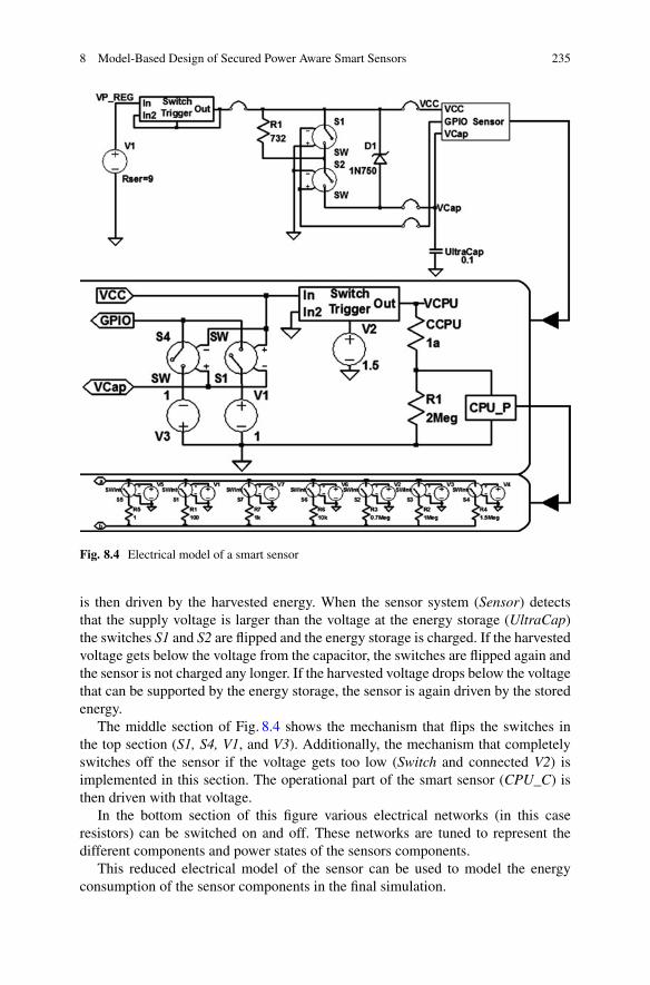
8 Model-Based Design of Secured Power Aware Smart Sensors 235
Fig. 8.4 Electrical model of a smart sensor
is then driven by the harvested energy. When the sensor system (Sensor) detectsthat the supply voltage is larger than the voltage at the energy storage (UltraCap)the switches S1 and S2 are flipped and the energy storage is charged. If the harvestedvoltage gets below the voltage from the capacitor, the switches are flipped again andthe sensor is not charged any longer. If the harvested voltage drops below the voltagethat can be supported by the energy storage, the sensor is again driven by the storedenergy.
The middle section of Fig. 8.4 shows the mechanism that flips the switches inthe top section (S1, S4, V1, and V3). Additionally, the mechanism that completelyswitches off the sensor if the voltage gets too low (Switch and connected V2) isimplemented in this section. The operational part of the smart sensor (CPU_C) isthen driven with that voltage.
In the bottom section of this figure various electrical networks (in this caseresistors) can be switched on and off. These networks are tuned to represent thedifferent components and power states of the sensors components.
This reduced electrical model of the sensor can be used to model the energyconsumption of the sensor components in the final simulation.
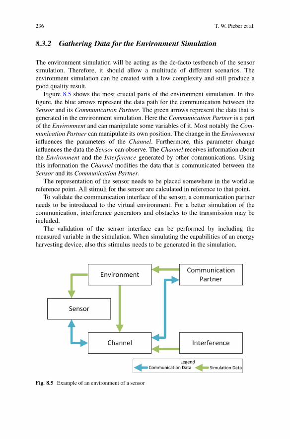
236 T. W. Pieber et al.
8.3.2 Gathering Data for the Environment Simulation
The environment simulation will be acting as the de-facto testbench of the sensorsimulation. Therefore, it should allow a multitude of different scenarios. Theenvironment simulation can be created with a low complexity and still produce agood quality result.
Figure 8.5 shows the most crucial parts of the environment simulation. In thisfigure, the blue arrows represent the data path for the communication between theSensor and its Communication Partner. The green arrows represent the data that isgenerated in the environment simulation. Here the Communication Partner is a partof the Environment and can manipulate some variables of it. Most notably the Com-munication Partner can manipulate its own position. The change in the Environmentinfluences the parameters of the Channel. Furthermore, this parameter changeinfluences the data the Sensor can observe. The Channel receives information aboutthe Environment and the Interference generated by other communications. Usingthis information the Channel modifies the data that is communicated between theSensor and its Communication Partner.
The representation of the sensor needs to be placed somewhere in the world asreference point. All stimuli for the sensor are calculated in reference to that point.
To validate the communication interface of the sensor, a communication partnerneeds to be introduced to the virtual environment. For a better simulation of thecommunication, interference generators and obstacles to the transmission may beincluded.
The validation of the sensor interface can be performed by including themeasured variable in the simulation. When simulating the capabilities of an energyharvesting device, also this stimulus needs to be generated in the simulation.
Fig. 8.5 Example of an environment of a sensor

8 Model-Based Design of Secured Power Aware Smart Sensors 237
This virtual environment allows the testing of the sensors use case. The environ-ment can be modified to test different use case scenarios, boundary conditions ofthe communication, and reaction of the sensor to faulty signals.
8.4 Creating the Simulations
When designing a new sensor, simulations play an essential role. Not only thesimulation of the sensor system, but also a simulation of the intended use case isuseful.
8.4.1 Designing the Sensor Model
Using the data gathered in Sect. 8.3.1 a model of a generic sensor can be createdusing SystemC. This models needs to represent all features of a smart sensor. Thesefeatures are:
• The sensor frontend: Depending on the use case the smart sensor can beequipped with different frontends. Typical frontends can just be switched on oroff, thus it can be modelled as a static energy consumer.
• The control unit: The microcontroller can be represented as a timed statemachine. Different power states that the microcontroller operates in can bedefined (e.g. calculating, memory access, idle, sleep).
• The memory: If the sensor includes an additional memory unit, a detaileddescription is needed. Typical memory modules have very few operational modes(data access, data write, sleep). These can be modelled very accurately withouthaving an overly complex model.
• The communication unit(s): The communication is typically slow and energyintensive. The model for the communication needs to be as accurate as possible.The description of the hardware itself can again be abstracted as a timed statemachine operating with different power levels (sending, receiving, sleep, energyharvesting).
• The energy provisioning system: Many sensors are either connected to a biggermachine or to the power grid. For those sensors we can assume the voltage tobe constant as it should be possible to provide sufficient energy to the sensor. Ifthe sensor is operated by a battery or using an energy harvesting system and acapacitor, this system needs to be modelled with high accuracy. Voltage drops dueto high energy demand can cause the sensor to stop operating. To counteract this,the sensor can use measures to decrease the energy consumption by temporarilydisabling some functionality. In addition to these radical changes to the energyconsumption, the non-linear behaviour of capacitors and batteries is important tothe accurate simulation of the voltage levels of the sensor.
• A security coprocessor: The modelling of a security coprocessor can be tricky asthe detailed description of it is most of the times classified. Nevertheless, a model
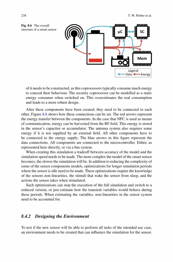
238 T. W. Pieber et al.
Fig. 8.6 The overallstructure of a smart sensor
of it needs to be constructed, as this coprocessors typically consume much energyto conceal their behaviour. The security coprocessor can be modelled as a staticenergy consumer when switched on. This overestimates the real consumptionand leads to a more robust design.
After these components have been created, they need to be connected to eachother. Figure 8.6 shows how these connections can be set. The red arrows representthe energy transfer between the components. In the case that NFC is used as meansof communication, energy can be harvested from the RF field. This energy is storedin the sensor’s capacitor or accumulator. The antenna system also requires someenergy if it is not supplied by an external field. All other components have tobe connected to the energy supply. The blue arrows in this figure represent thedata connections. All components are connected to the microcontroller. Either, asrepresented here directly, or via a bus system.
When creating this simulation a tradeoff between accuracy of the model and thesimulation speed needs to be made. The more complex the model of the smart sensorbecomes, the slower the simulation will be. In addition to reducing the complexity ofsome of the sensor components models, optimizations for longer simulation periodswhere the sensor is idle need to be made. These optimizations require the knowledgeof the sensors non-linearities, the stimuli that wake the sensor from sleep, and theactions the sensor takes when stimulated.
Such optimizations can stop the execution of the full simulation and switch to areduced version, or just estimate how the transient variables would behave duringthese periods. When estimating the variables, non-linearities in the sensor systemneed to be accounted for.
8.4.2 Designing the Environment
To test if the new sensor will be able to perform all tasks of the intended use case,an environment needs to be created that can influence the simulation for the sensor.

8 Model-Based Design of Secured Power Aware Smart Sensors 239
The environment can be simulated using the “Gazebo” simulator. To describe thedifferent actions an entity can take, plugins need to be created. This simulation canthen be used as a testbench for the sensor simulation. Using the data from Sect. 8.3.2a model of the environment can be created. Its vital components are:
• The sensor: A representation of the sensor in the environment. This componentimplements the interface to the sensor simulation. All interactions of theenvironment with the sensor are relative to this representation. Additionally, allparameters the simulation calculates for the sensor to measure are calculated withthis reference model.
• Something to measure: A simulation tool representing 3D objects primarilycomputes the relative motion and size between objects. Other parameters suchas communication signals, air humidity, temperature, or light might not becalculated. Depending on the use case of the sensor these variables need to becalculated and passed to the sensor model.
• A communication partner: To test the communication unit of the sensor acounterpart needs to be implemented in the environment. This can be performedby another instance of the new sensor or an already existing device. To be able totest different scenarios it can be useful to allow the communication partner to bemoved.
• Interference and obstacles: Any communication is influenced by the environ-ment it is performed in. In the case of a wireless communication interferencefrom other machinery, nearby communication, signal attenuation, and the scat-tering and reflecting of the signal produce communication errors. To see howthe sensor reacts to faulty messages an implementation of the communicationchannel, including some interferences, is needed.
These components are then placed in a 3D virtual environment and logicallyconnected.
The sensor receives information about the communication from the implemen-tation of the channel and information about the measured variable directly fromthe environment. This data is then forwarded to the sensor simulation. The datathat is produced by the sensor simulation is filtered and forwarded to the intendeddestination. This destination can be an actuator or the communication channel.
The communication partner sends the information that is intended for the sensorto the communication channel and receives the information from the sensor viathis channel. If the communication partner is movable, the information about thechanging position is sent to the environment.
The channel receives data from all communication partners and noise sources.Additionally, information about the 3D environment is gathered. Using this infor-mation the received data is modified (bit errors are introduced and the transmittedenergy is calculated) and sent to the receiver.
The environment gathers data about the location of all objects. The informationabout the measured variable is then calculated and sent to the sensor.
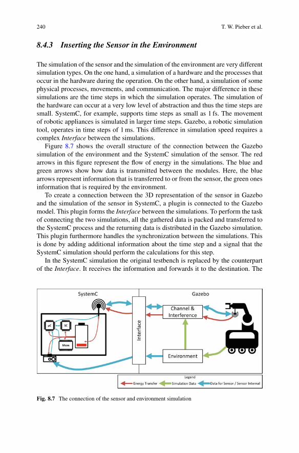
240 T. W. Pieber et al.
8.4.3 Inserting the Sensor in the Environment
The simulation of the sensor and the simulation of the environment are very differentsimulation types. On the one hand, a simulation of a hardware and the processes thatoccur in the hardware during the operation. On the other hand, a simulation of somephysical processes, movements, and communication. The major difference in thesesimulations are the time steps in which the simulation operates. The simulation ofthe hardware can occur at a very low level of abstraction and thus the time steps aresmall. SystemC, for example, supports time steps as small as 1 fs. The movementof robotic appliances is simulated in larger time steps. Gazebo, a robotic simulationtool, operates in time steps of 1 ms. This difference in simulation speed requires acomplex Interface between the simulations.
Figure 8.7 shows the overall structure of the connection between the Gazebosimulation of the environment and the SystemC simulation of the sensor. The redarrows in this figure represent the flow of energy in the simulations. The blue andgreen arrows show how data is transmitted between the modules. Here, the bluearrows represent information that is transferred to or from the sensor, the green onesinformation that is required by the environment.
To create a connection between the 3D representation of the sensor in Gazeboand the simulation of the sensor in SystemC, a plugin is connected to the Gazebomodel. This plugin forms the Interface between the simulations. To perform the taskof connecting the two simulations, all the gathered data is packed and transferred tothe SystemC process and the returning data is distributed in the Gazebo simulation.This plugin furthermore handles the synchronization between the simulations. Thisis done by adding additional information about the time step and a signal that theSystemC simulation should perform the calculations for this step.
In the SystemC simulation the original testbench is replaced by the counterpartof the Interface. It receives the information and forwards it to the destination. The
Fig. 8.7 The connection of the sensor and environment simulation
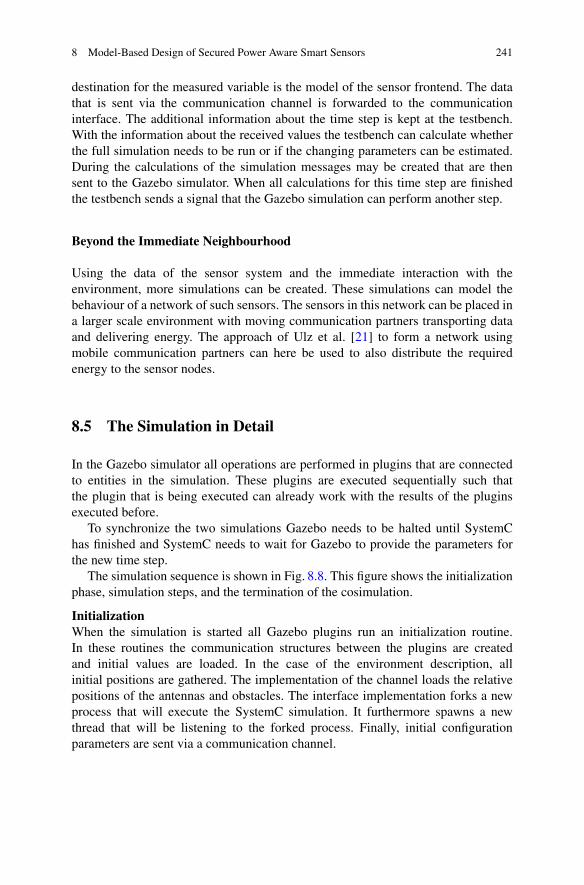
8 Model-Based Design of Secured Power Aware Smart Sensors 241
destination for the measured variable is the model of the sensor frontend. The datathat is sent via the communication channel is forwarded to the communicationinterface. The additional information about the time step is kept at the testbench.With the information about the received values the testbench can calculate whetherthe full simulation needs to be run or if the changing parameters can be estimated.During the calculations of the simulation messages may be created that are thensent to the Gazebo simulator. When all calculations for this time step are finishedthe testbench sends a signal that the Gazebo simulation can perform another step.
Beyond the Immediate Neighbourhood
Using the data of the sensor system and the immediate interaction with theenvironment, more simulations can be created. These simulations can model thebehaviour of a network of such sensors. The sensors in this network can be placed ina larger scale environment with moving communication partners transporting dataand delivering energy. The approach of Ulz et al. [21] to form a network usingmobile communication partners can here be used to also distribute the requiredenergy to the sensor nodes.
8.5 The Simulation in Detail
In the Gazebo simulator all operations are performed in plugins that are connectedto entities in the simulation. These plugins are executed sequentially such thatthe plugin that is being executed can already work with the results of the pluginsexecuted before.
To synchronize the two simulations Gazebo needs to be halted until SystemChas finished and SystemC needs to wait for Gazebo to provide the parameters forthe new time step.
The simulation sequence is shown in Fig. 8.8. This figure shows the initializationphase, simulation steps, and the termination of the cosimulation.
InitializationWhen the simulation is started all Gazebo plugins run an initialization routine.In these routines the communication structures between the plugins are createdand initial values are loaded. In the case of the environment description, allinitial positions are gathered. The implementation of the channel loads the relativepositions of the antennas and obstacles. The interface implementation forks a newprocess that will execute the SystemC simulation. It furthermore spawns a newthread that will be listening to the forked process. Finally, initial configurationparameters are sent via a communication channel.
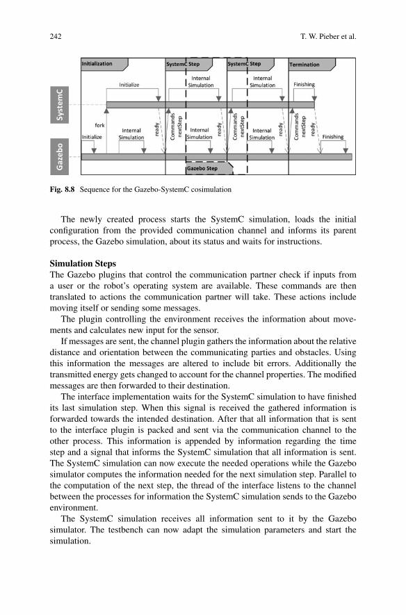
242 T. W. Pieber et al.
Fig. 8.8 Sequence for the Gazebo-SystemC cosimulation
The newly created process starts the SystemC simulation, loads the initialconfiguration from the provided communication channel and informs its parentprocess, the Gazebo simulation, about its status and waits for instructions.
Simulation StepsThe Gazebo plugins that control the communication partner check if inputs froma user or the robot’s operating system are available. These commands are thentranslated to actions the communication partner will take. These actions includemoving itself or sending some messages.
The plugin controlling the environment receives the information about move-ments and calculates new input for the sensor.
If messages are sent, the channel plugin gathers the information about the relativedistance and orientation between the communicating parties and obstacles. Usingthis information the messages are altered to include bit errors. Additionally thetransmitted energy gets changed to account for the channel properties. The modifiedmessages are then forwarded to their destination.
The interface implementation waits for the SystemC simulation to have finishedits last simulation step. When this signal is received the gathered information isforwarded towards the intended destination. After that all information that is sentto the interface plugin is packed and sent via the communication channel to theother process. This information is appended by information regarding the timestep and a signal that informs the SystemC simulation that all information is sent.The SystemC simulation can now execute the needed operations while the Gazebosimulator computes the information needed for the next simulation step. Parallel tothe computation of the next step, the thread of the interface listens to the channelbetween the processes for information the SystemC simulation sends to the Gazeboenvironment.
The SystemC simulation receives all information sent to it by the Gazebosimulator. The testbench can now adapt the simulation parameters and start thesimulation.
8 Model-Based Design of Secured Power Aware Smart Sensors 243
While the simulation is being executed messages can be sent to the Gazebosimulator. These messages can originate from the communication interface module.If this sensor also includes an actuator or some visual status indicator, these modulescan also send information to the environment simulation.
When the simulation step is finished the testbench sends the signal that thesimulation step is finished.
TerminationAfter the simulation has been performed the plugins receive a signal that thesimulation is about to be ended.
The interface plugin relays this information and waits for the remaining messagesfrom SystemC. When it receives a signal that the SystemC simulation is terminatedthe plugin cleans its data structures and terminates.
When the SystemC simulation receives the signal to terminate, a post-processingstep for the gathered data is initiated. This post-processing is a part of the runtimeoptimizations and performs tasks to correctly display the gathered data. The data isfurthermore compressed by the post-processing step. Finally the data is saved andthe Gazebo simulation is informed of the termination of the simulation.
8.5.1 Optimizations
As the SystemC simulation operates in smaller time steps, each step of theGazebo simulation causes thousands of SystemC steps. This results in the SystemCsimulation being much slower than the Gazebo one, and thus slowing down thewhole process. To speed up the simulation, the accuracy of the results can be reducedat certain times. A possible method to reduce the accuracy is shown in Fig. 8.9.
To take advantages of this possibility, the testbench needs to estimate the stateafter the simulation step. If the sensor is in idle mode and the input parameters donot change, the accuracy can be reduced by skipping the simulation and keepinga number that describes the amount of time that has been skipped since the last
Fig. 8.9 The testbench of the SystemC simulation is adapted to skip the simulation if it is likelyto yield results that can be estimated
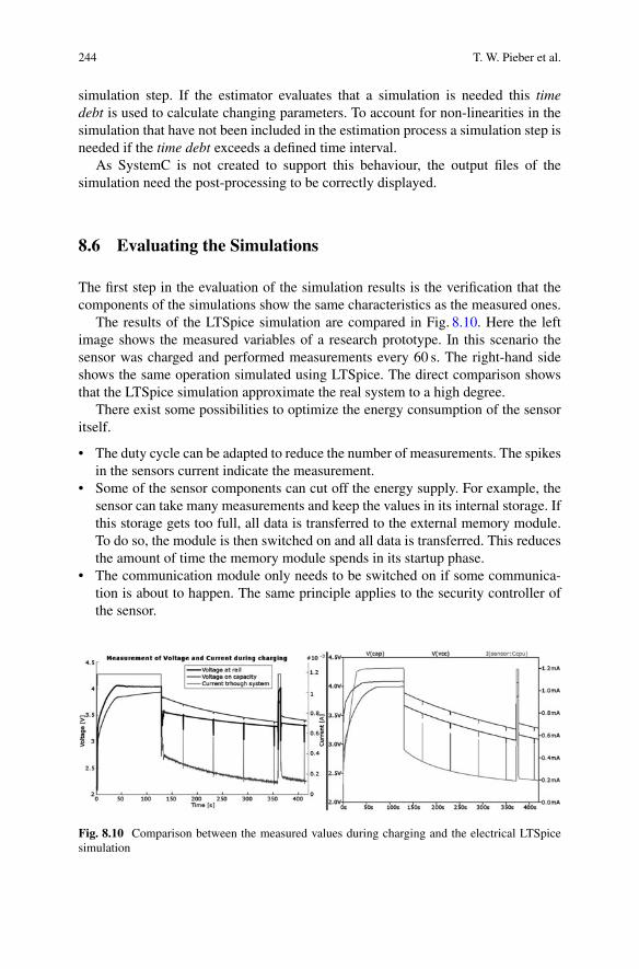
244 T. W. Pieber et al.
simulation step. If the estimator evaluates that a simulation is needed this timedebt is used to calculate changing parameters. To account for non-linearities in thesimulation that have not been included in the estimation process a simulation step isneeded if the time debt exceeds a defined time interval.
As SystemC is not created to support this behaviour, the output files of thesimulation need the post-processing to be correctly displayed.
8.6 Evaluating the Simulations
The first step in the evaluation of the simulation results is the verification that thecomponents of the simulations show the same characteristics as the measured ones.
The results of the LTSpice simulation are compared in Fig. 8.10. Here the leftimage shows the measured variables of a research prototype. In this scenario thesensor was charged and performed measurements every 60 s. The right-hand sideshows the same operation simulated using LTSpice. The direct comparison showsthat the LTSpice simulation approximate the real system to a high degree.
There exist some possibilities to optimize the energy consumption of the sensoritself.
• The duty cycle can be adapted to reduce the number of measurements. The spikesin the sensors current indicate the measurement.
• Some of the sensor components can cut off the energy supply. For example, thesensor can take many measurements and keep the values in its internal storage. Ifthis storage gets too full, all data is transferred to the external memory module.To do so, the module is then switched on and all data is transferred. This reducesthe amount of time the memory module spends in its startup phase.
• The communication module only needs to be switched on if some communica-tion is about to happen. The same principle applies to the security controller ofthe sensor.
Fig. 8.10 Comparison between the measured values during charging and the electrical LTSpicesimulation
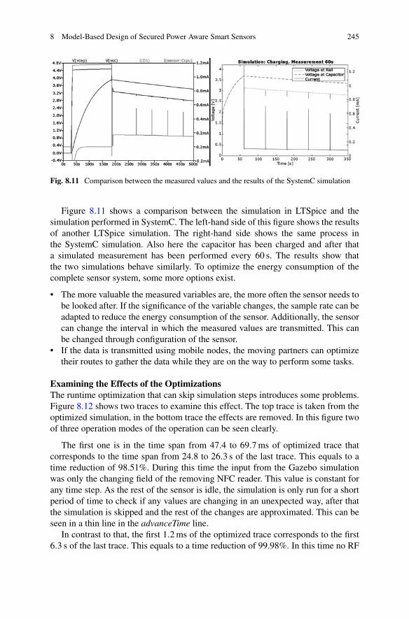
8 Model-Based Design of Secured Power Aware Smart Sensors 245
Fig. 8.11 Comparison between the measured values and the results of the SystemC simulation
Figure 8.11 shows a comparison between the simulation in LTSpice and thesimulation performed in SystemC. The left-hand side of this figure shows the resultsof another LTSpice simulation. The right-hand side shows the same process inthe SystemC simulation. Also here the capacitor has been charged and after thata simulated measurement has been performed every 60 s. The results show thatthe two simulations behave similarly. To optimize the energy consumption of thecomplete sensor system, some more options exist.
• The more valuable the measured variables are, the more often the sensor needs tobe looked after. If the significance of the variable changes, the sample rate can beadapted to reduce the energy consumption of the sensor. Additionally, the sensorcan change the interval in which the measured values are transmitted. This canbe changed through configuration of the sensor.
• If the data is transmitted using mobile nodes, the moving partners can optimizetheir routes to gather the data while they are on the way to perform some tasks.
Examining the Effects of the OptimizationsThe runtime optimization that can skip simulation steps introduces some problems.Figure 8.12 shows two traces to examine this effect. The top trace is taken from theoptimized simulation, in the bottom trace the effects are removed. In this figure twoof three operation modes of the operation can be seen clearly.
The first one is in the time span from 47.4 to 69.7 ms of optimized trace thatcorresponds to the time span from 24.8 to 26.3 s of the last trace. This equals to atime reduction of 98.51%. During this time the input from the Gazebo simulationwas only the changing field of the removing NFC reader. This value is constant forany time step. As the rest of the sensor is idle, the simulation is only run for a shortperiod of time to check if any values are changing in an unexpected way, after thatthe simulation is skipped and the rest of the changes are approximated. This can beseen in a thin line in the advanceTime line.
In contrast to that, the first 1.2 ms of the optimized trace corresponds to the first6.3 s of the last trace. This equals to a time reduction of 99.98%. In this time no RF
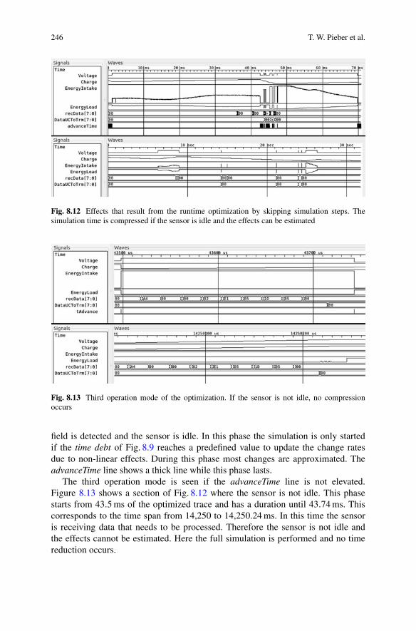
246 T. W. Pieber et al.
Fig. 8.12 Effects that result from the runtime optimization by skipping simulation steps. Thesimulation time is compressed if the sensor is idle and the effects can be estimated
Fig. 8.13 Third operation mode of the optimization. If the sensor is not idle, no compressionoccurs
field is detected and the sensor is idle. In this phase the simulation is only startedif the time debt of Fig. 8.9 reaches a predefined value to update the change ratesdue to non-linear effects. During this phase most changes are approximated. TheadvanceTime line shows a thick line while this phase lasts.
The third operation mode is seen if the advanceTime line is not elevated.Figure 8.13 shows a section of Fig. 8.12 where the sensor is not idle. This phasestarts from 43.5 ms of the optimized trace and has a duration until 43.74 ms. Thiscorresponds to the time span from 14,250 to 14,250.24 ms. In this time the sensoris receiving data that needs to be processed. Therefore the sensor is not idle andthe effects cannot be estimated. Here the full simulation is performed and no timereduction occurs.

8 Model-Based Design of Secured Power Aware Smart Sensors 247
The values of the simulation time reduction highly depend on the processor stateand the simulated use case.
8.7 Security of Smart Sensors
When developing new sensors, not only the efficiency of them is important, theyfurthermore should be secure. The security should not only care about the data thatis generated by the sensor, but also the sensors should not endanger systems theyare connected to.
Any security solution for smart sensors needs to consider the following sixpoints:
• The sensor has limited resources in terms of energy and processing power.• The overhead in memory usage, computational effort, and data transmission sizes
that are imposed due to security considerations can be large in comparison withthe payload data.
• To provide security to a sensor network every sensor needs to perform thesecurity relevant operations.
• The security features should be easy to use by untrained end users.• The end user needs to trust the security features of the sensor.• Dedicated hardware that performs the security operations is better, but needs
more energy and can be costly.
8.7.1 Data Security
The sensor data needs to be protected from unauthorized access. Otherwise this datacan disclose company secrets. Furthermore, if the sensor data can be replicated,control mechanisms can be fooled to perform harmful operations that can endangerthe facility or human lives. In the case of the STUXNET attack [9] the attacker haslearned the behaviour of the system by observing the sensor data. After the learningphase the attacker manipulated the sensor’s data to turbines of a nuclear enrichmentplant while it was hiding its doings by displaying normal looking data to the nextlayer of controls.
This attack showed that the sensor data needs to be protected. To be able to read(or guess) the sensor data can enable an attacker to manipulate the processes theyobserve.
To protect the gathered data in a sensor network from unauthorized access, thedata needs to be encrypted. As Ulz et al. showed, such measures increase the severityof introduced bit errors [24]. To still be able to communicate correctly, a forwarderror correction scheme can be used on the encrypted data. Using this method, biterrors can be detected before decrypting, thus increasing the resilience against biterrors of the communication. Ulz et al. also suggested a solution to this problemwhich they called Joint Encryption and Error Correction (JEEC).
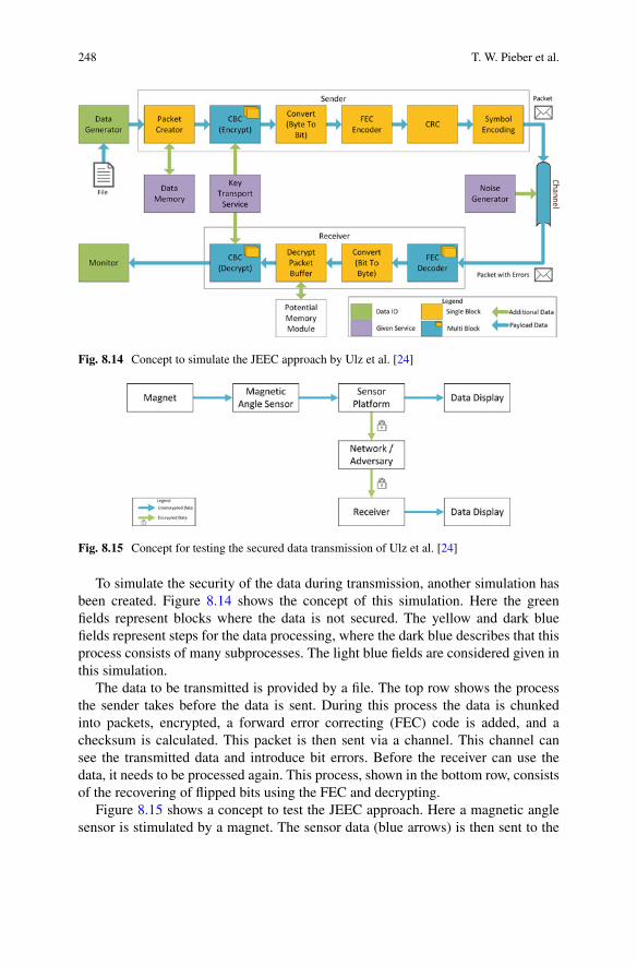
248 T. W. Pieber et al.
Fig. 8.14 Concept to simulate the JEEC approach by Ulz et al. [24]
Fig. 8.15 Concept for testing the secured data transmission of Ulz et al. [24]
To simulate the security of the data during transmission, another simulation hasbeen created. Figure 8.14 shows the concept of this simulation. Here the greenfields represent blocks where the data is not secured. The yellow and dark bluefields represent steps for the data processing, where the dark blue describes that thisprocess consists of many subprocesses. The light blue fields are considered given inthis simulation.
The data to be transmitted is provided by a file. The top row shows the processthe sender takes before the data is sent. During this process the data is chunkedinto packets, encrypted, a forward error correcting (FEC) code is added, and achecksum is calculated. This packet is then sent via a channel. This channel cansee the transmitted data and introduce bit errors. Before the receiver can use thedata, it needs to be processed again. This process, shown in the bottom row, consistsof the recovering of flipped bits using the FEC and decrypting.
Figure 8.15 shows a concept to test the JEEC approach. Here a magnetic anglesensor is stimulated by a magnet. The sensor data (blue arrows) is then sent to the

8 Model-Based Design of Secured Power Aware Smart Sensors 249
smart sensor platform where it is processed. The original data gets displayed forlater comparison. Additionally, the sensor data gets encrypted and encoded usinga FEC scheme. This packed data is then sent via a network to the receiver (greenarrows with locks). The adversary is in the network and can manipulate the data.The receiver tries to decode the data. If this succeeds the plain data is displayed tobe compared against the original one.
8.7.2 System Security
Recently another kind of attack using sensors has been reported. In this scenarioa large number of sensors connected to a network are used to perform a DDoS(Distributed Denial of Service) attack. In this type of attack the sensors firmwareis altered to send messages through the network to a common destination. Using alarge number of manipulated sensors, the common destination receives more datathan it can handle. This blocks the recipients capabilities to perform its normaloperations.
To use the sensors for such malicious purposes, their firmware needs to bechanged. Ulz et al. presented an approach to exclude sensors from the sensornetwork that use unauthorized firmware [22]. This is done in a two-layer system.In the first step the firmware is checked by an on-board security module. If thischeck verifies that the software is from a trusted source, the sensor’s network stackis released. Now the firmware version can be checked at a trusted backend server.This verifies that the sensor is running the newest version of the firmware.
8.8 Conclusions
This chapter presents an approach to design secured power aware smart sensorsusing hardware models. To be able to use this model-based design, the modelparameters need to be known. Therefore, we discussed the methods for gatheringsuch data and how the data can be simplified to be used in an abstracted hardwaremodel. In addition to the model, use cases for the new sensor need to be known.Here a simple simulation can be performed that generates the inputs necessary forthe hardware simulation. If the use case extends beyond one sensor, the gathereddata can be abstracted again and included in higher layer simulations. Additionally,we presented the main phases of such simulations and mentioned possibilities forruntime optimizations. Finally, we discussed the possibilities of attacks on andwith the sensors and mentioned methods to increase the difficulty of a successfulattack. Additionally, the concepts to secure the data against adversaries has alsobeen simulated and tested.

250 T. W. Pieber et al.
As the simulation should resemble a generic smart sensor, some details are lostat every layer of abstraction of the models. This loss in detail is necessary to createusable simulations.
The main focus of this chapter is on the creation of the simulation of such sensorsystems. A detailed description on the model generation and the simulation steps isgiven.
Using these simulations it is possible to analyse the effects of changes to thesensor system, the communication protocols, or the routines in the environment.This can be used to optimize the energy consumption of each individual componentsas well as the energy consumption of the complete environment.
Acknowledgements This project has received funding from the Electronic Component Systemsfor European Leadership Joint Undertaking under grant agreement No 692480. This JointUndertaking receives support from the European Union’s Horizon 2020 research and innovationprogramme and Germany, Netherlands, Spain, Austria, Belgium, Slovakia.
IoSense is funded under the agreement number 853326 by the Austrian Federal Ministry ofTransport, Innovation and Technology (BMVIT) under the program “ICT of the Future” betweenMay 2016 and May 2019. More information https://iktderzukunft.at/en/.
We would like to thank Infineon Technologies and especially Rainer Matischek for providing usthe security controllers used in the system and for their support that helped creating the prototypesand simulations.
References
1. Accelera: SystemC. (2000). http://accellera.org/downloads/standards/systemc. Accessed 17Jan 2017
2. M. Antonakakis, T. April, M. Bailey, M. Bernhard, E. Bursztein, J. Cochran, Z. Durumeric,J.A. Halderman, L. Invernizzi, M. Kallitsis, et al., Understanding the Mirai botnet, in USENIXSecurity Symposium (2017)
3. F. Bouchhima, M. Briere, G. Nicolescu, M. Abid, E. Aboulhamid, A SystemC/simulink co-simulation framework for continuous/discrete-events simulation, in 2006 IEEE InternationalBehavioral Modeling and Simulation Workshop (Institute of Electrical and Electronics Engi-neers (IEEE), Piscataway, 2006). https://doi.org/10.1109/bmas.2006.283461
4. R.J. Campbell, Cybersecurity issues for the bulk power system. Electr. Deliv. Secur FedOversight Activities Funding, 63–108 (2016). https://www.hsdl.org/?abstract&did=767255
5. G. Chen, M. Fojtik, D. Kim, D. Fick, J. Park, M. Seok, M.T. Chen, Z. Foo, D. Sylvester, D.Blaauw, Millimeter-scale nearly perpetual sensor system with stacked battery and solar cells, in2010 IEEE International Solid-State Circuits Conference - (ISSCC) (IEEE, Piscataway, 2010).https://doi.org/10.1109/isscc.2010.5433921
6. J. Haase, D. Meyer, M. Eckert, B. Klauer, Wireless sensor/actuator device configurationby NFC, in 2016 IEEE International Conference on Industrial Technology (ICIT) (IEEE,Piscataway, 2016), pp. 1336–1340
7. K. Huang, I. Bacivarov, F. Hugelshofer, L. Thiele, Scalably distributed SystemC simulationfor embedded applications, in 2008 International Symposium on Industrial Embedded Systems(Institute of Electrical and Electronics Engineers (IEEE), Piscataway, 2008). https://doi.org/10.1109/sies.2008.4577715
8. A. Kansal, J. Hsu, S. Zahedi, M.B. Srivastava, Power management in energy harvestingsensor networks. ACM Trans. Embed. Comput. Syst. 6(4), 32 (2007). https://doi.org/10.1145/1274858.1274870
8 Model-Based Design of Secured Power Aware Smart Sensors 251
9. R. Langner, Stuxnet: dissecting a cyberwarfare weapon. IEEE Secur. Priv. 9(3), 49–51 (2011)10. W.S. Lee, W.I. Son, K.S. Oh, J.W. Yu, Contactless energy transfer systems using antiparallel
resonant loops. IEEE Trans. Ind. Electron. 60(1), 350–359 (2013). https://doi.org/10.1109/tie.2011.2177611
11. D. Martin, P. Wilsey, R. Hoekstra, E. Keiter, S. Hutchinson, T. Russo, L. Waters, Integratingmultiple parallel simulation engines for mixed-technology parallel simulation, in Proceedings35th Annual Simulation Symposium. SS 2002 (Institute of Electrical and Electronics Engineers(IEEE), Piscataway, 2002). https://doi.org/10.1109/simsym.2002.1000082
12. Mathworks: get started with gazebo and a simulated turtlebot (2016). https://de.mathworks.com/help/robotics/examples/get-started-with-gazebo-and-a-simulated-turtlebot.html.Accessed 03 Jan 2017
13. D. Mueller-Gritschneder, K. Lu, E. Wallander, M. Greim, U. Schlichtmann, A virtual proto-typing platform for real-time systems with a case study for a two-wheeled robot, in Design,Automation & Test in Europe Conference & Exhibition (DATE), 2013 (EDAA, 2013). https://doi.org/10.7873/date.2013.274
14. Open Source Robotics Foundation: Gazebo simulator (2004). http://www.gazebosim.org.Accessed 03 Jan 2017
15. P.R. Panda, SystemC - A modelling platform supporting multiple design abstractions, inProceedings of the 14th International Symposium on Systems Synthesis - ISSS (Associationfor Computing Machinery (ACM), New York, 2001). https://doi.org/10.1145/500001.500018
16. T.W. Pieber, T. Ulz, C. Steger, Systemic test case generation with the gazebo simulator, inProceedings of the 7th International Conference on Simulation and Modeling Methodologies,Technologies and Applications - Volume 1: SIMULTECH. INSTICC, (SciTePress, Setúbal,2017). https://doi.org/10.5220/0006404800650072
17. T.W. Pieber, T. Ulz, C. Steger, R. Matischek, Hardware secured, password-based authenticationfor smart sensors for the industrial internet of things, in International Conference on Networkand System Security (Springer, Berlin, 2017), pp. 632–642
18. H. Possadas, J.A. Adamez, E. Villar, F. Blasco, F. Escuder, RTOS modeling in SystemCfor real-time embedded SW simulation: a POSIX model. Des. Autom. Embed. Syst. (2005).https://doi.org/10.1007/s10617-006-9725-1
19. M. Rahimi, H. Shah, G. Sukhatme, J. Heideman, D. Estrin, Studying the feasibility of energyharvesting in a mobile sensor network, in 2003 IEEE International Conference on Robotics andAutomation (Cat. No.03CH37422) (IEEE, Piscataway, 2003). https://doi.org/10.1109/robot.2003.1241567
20. T. Sogorb, J.V. Llario, J. Pelegri, R. Lajara, J. Alberola, Studying the feasibility of energy har-vesting from broadcast RF station for WSN, in Instrumentation and Measurement TechnologyConference Proceedings, 2008, IMTC’08 (IEEE, Piscataway, 2008). pp. 1360–1363
21. T. Ulz, T. Pieber, C. Steger, S. Haas, R. Matischek, Sneakernet on wheels: trustworthy NFC-based robot to machine communication, in 2017 IEEE International Conference on RFIDTechnology & Application (RFID-TA) (IEEE, Piscataway, 2017), pp. 260–265
22. T. Ulz, T. Pieber, C. Steger, S. Haas, R. Matischek, H. Bock, Hardware-secured configurationand two-layer attestation architecture for smart sensors, in 2017 Euromicro Conference onDigital System Design (DSD) (IEEE, Piscataway, 2017), pp. 229–236
23. T. Ulz, T. Pieber, C. Steger, C. Lesjak, H. Bock, R. Matischek, Secureconfig: NFC and QR-codebased hybrid approach for smart sensor configuration, in 2017 IEEE International Conferenceon RFID (IEEE, Piscataway, 2017), pp. 41–46
24. T. Ulz, T. Pieber, C. Steger, R. Matischek, H. Bock, Towards trustworthy data in networkedcontrol systems: a hardware-based approach, in 2017 22nd IEEE International Conference onEmerging Technologies and Factory Automation (ETFA) (IEEE, Piscataway, 2017), pp. 1–8
25. R. Yan, H. Sun, Y. Qian, Energy-aware sensor node design with its application in wirelesssensor networks. IEEE Trans. Instrum. Meas. 62(5), 1183–1191 (2013). https://doi.org/10.1109/tim.2013.2245181
26. I. Zamora, N.G. Lopez, V.M. Vilches, A.H. Cordero, Extending the OpenAI Gym for robotics:a toolkit for reinforcement learning using ROS and Gazebo. arXiv preprint arXiv:1608.05742(2016)
Chapter 9A Software Toolkit for Complex SensorSystems in Fog Environments
Dominik Grzelak, Carl Mai, René Schöne, Jan Falkenberg, and Uwe Aßmann
9.1 Introduction
The Software Toolkit (STK) is a component-oriented framework, which facilitatesthe integration of single sensors, sensor arrays, and complex sensor systems in thefog. It is developed with the vision of prospective use for different applicationdomains (e.g., manufacturing or smart home), where the properties of the STKare designed in such a way to follow domain-specific standards and considersupplementary conditions for particular domains. The goal of the STK is to providethe functional coupling between the system environment and the sensor elements aswell as realizing the efficient and secure data aspects between sub-systems and theapplication’s main system. From low-level sensor signals to a complex IoT system,multiple connected sensors are the key elements of emerging smart rooms, whichrequire a unified software framework to create value-adding applications (apps) fora future smart room software ecosystem. With the STK, a focus on aspects regardingreliability, weight, cost, performance, interoperability, and standardization was set.Furthermore, the software toolkit facilitates the application of new developments bythird-party users or system developers.
9.1.1 Motivation
In the next years more and more things and information will be connected to theinternet resulting in a complex network, which becomes denser with every single
D. Grzelak (�) · C. Mai · R. Schöne · J. Falkenberg · U. AßmannTU Dresden, Fakultät Informatik—Institut für Software- und Multimediatechnik/LehrstuhlSoftwaretechnologie, Dresden, Germanye-mail: [email protected]
© Springer Nature Switzerland AG 2020W. D. van Driel et al. (eds.), Sensor Systems Simulations,https://doi.org/10.1007/978-3-030-16577-2_9
253
254 D. Grzelak et al.
device—this is referred to as the Internet of Things (IoT). A huge variety and amountof data are generated from various devices and sensors, which need to be processedand responded to in near real-time with the cloud becoming an indispensable part ofthat process. It is expected that 50 billion devices will be connected to the Internetby 2020 [1].
Because IoT is becoming more prominent and the number of devices is steadilyincreasing, smart objects and devices equipped with sensors will become animportant source of data as they can gather different information not only fromtheir internal states but also about the environment and entities they interact with.This data is used as a basis for various kinds of decision algorithms, machinelearning, and artificial intelligence in general. Hence, the importance of collectingand distributing this data to the right services. On the flip side, this will also producemore and more traffic in the network and become a burden for low-bandwidth andhigh-latency networks.
A purely cloud-based solution is not able to overcome these issues as the physicaldistance between the user, edge devices, and the cloud services increase with thetransmission latency and response times. Therefore, complex real-time applicationsare not possible anymore. The next logical step is to push the cloud services tothe edge of the network—to the devices (e.g., sensors, actuators, and embeddedcomputers) gathering the actual data, moving the processing of data closer to theedge as well. Deriving higher-level data and performing decisions locally on thosedevices instead of a physically distant cloud server will significantly reduce theamount of data that is being sent through the network, reduce the required bandwidthand also increase data security. These are the main principles of Fog Computing [2],which we will use as the basic paradigm for developing a software architecture andthe IoSense Software Toolkit to facilitate the integration of newly developed sensorsfrom IoSense with the existing IoT infrastructure.
The goal of the software toolkit is to bridge the gap between the cloud andconnected sensors (e.g., the newly developed light sources), as shown in Fig. 9.1. Todemonstrate complex scenarios with an installation of sensors, actuators, or sensorarrays in combination with the software system, we present a component-basedsoftware architecture, which copes with each of the challenges mentioned above.Also, the architecture intends to facilitate the integration and interaction of new andexisting IoT devices of different vendors (e.g., sensors and actuators).
To overcome above problems, the STK provides a solution to the issues above:a decentralized system architecture based on fog computing paradigms and asoftware framework providing a feasible solution for integrating a wide rangeof sensors in complex systems and systems of systems. The STK uses recentlydeveloped concepts to leverage the separation of important functionality into smallcomponents, which can be reused and distributed to various kinds of heterogeneousdevices (such as single-board computers, and sensor systems). The STK makes theintegration of and communication among all IoT components as easy as possible.The processing of data and execution of the workload directly on a device closer tothe user’s network is speeding up applications that require low-latency responses.Even if they are not continuously connected to the network, devices can make smart
9 A Software Toolkit for Complex Sensor Systems in Fog Environments 255
Fig. 9.1 The software architecture bridging the gap between a connected sensor system in the IoTlayer and the cloud services
decisions and send the data at a later point in time. That is a crucial requirementwhen developing complex sensor system applications in IoT environments withresource constraints and dynamic, mobile devices.
9.1.2 Structure
Fog can handle the diversity of different industry standards, sensors, devices, and soon. Therefore, Section Background describes the underlying computing conceptsand properties that are vital for the development of the fog-based framework.
The key element of a fog computing framework can bring its elements regardingcommunication and self-adaption in conformity with the fog paradigms. In SectionArchitecture, the architecture of the STK is introduced where the presentedconcepts of the previous section are adopted.
The development of the STK is based on several demonstrators and use cases.In Section Evaluation, the evaluation is guided by three case studies, involving the

256 D. Grzelak et al.
implementation of robot control applications and a person-dependent illuminationsystem. We chose this kind of scenario to demonstrate how the STK can handlemulti-sensor and multi-actor integration.
In Section Related Work, we are comparing the STK with other frameworksfound in the scientific literature.
Finally, conclusions are offered in Section Summary.
9.2 Background: Software and System Engineering Conceptsfor Fog Computing
In this section, we introduce the foundations for the work on the software toolkitby examining various computing concepts and methods of sensor integration.Combining this with our goals to produce a versatile and distributed system, weexplain our choice in Section Architecture.
9.2.1 Computing Concepts
In the area of IoT, there are various computing concepts employed because of theheterogeneous hardware and the various requirements on an IoT system. Here wewill explain the most important concepts, which all are part of the considerations toimplement the STK.
9.2.1.1 Embedded
Embedded systems purely integrate the entire processing capability into a microcon-troller. Potential collaborations with other embedded systems are defined at designtime due to their inability to change the firmware code during runtime. However,modern microcontrollers use standard communication protocols (e.g., TCP/IP)to communicate with others. The computational performance of microcontrollersis usually very limited. Therefore, only simple tasks such as non-intensive dataprocessing and data analysis can be performed.
9.2.1.2 On-Premise
In many cases, an embedded system is accompanied by a computer (e.g., localcomputer or server) with higher performance and more storage on premise (inthe building) of the person or organization. The computer usually uses an ×86architecture and a high-level operating system (e.g., Linux). In this way, the long-
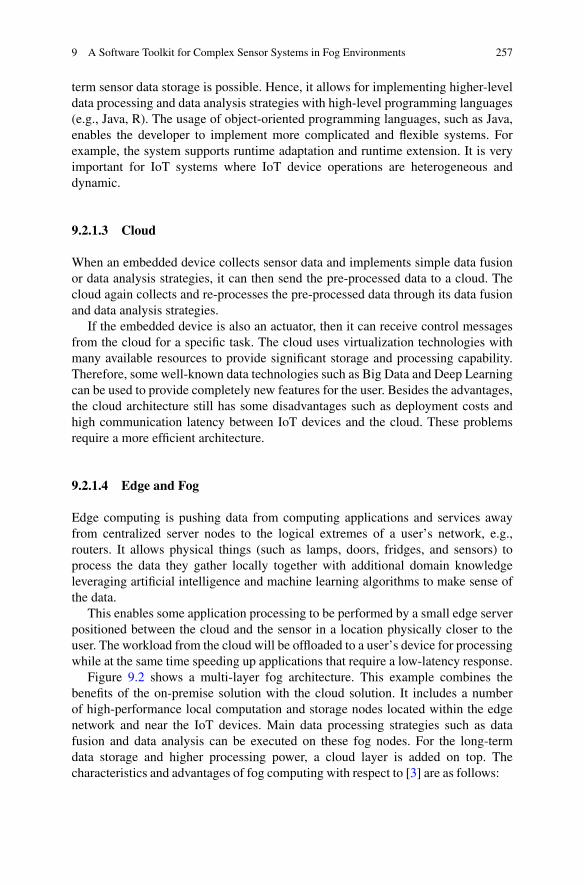
9 A Software Toolkit for Complex Sensor Systems in Fog Environments 257
term sensor data storage is possible. Hence, it allows for implementing higher-leveldata processing and data analysis strategies with high-level programming languages(e.g., Java, R). The usage of object-oriented programming languages, such as Java,enables the developer to implement more complicated and flexible systems. Forexample, the system supports runtime adaptation and runtime extension. It is veryimportant for IoT systems where IoT device operations are heterogeneous anddynamic.
9.2.1.3 Cloud
When an embedded device collects sensor data and implements simple data fusionor data analysis strategies, it can then send the pre-processed data to a cloud. Thecloud again collects and re-processes the pre-processed data through its data fusionand data analysis strategies.
If the embedded device is also an actuator, then it can receive control messagesfrom the cloud for a specific task. The cloud uses virtualization technologies withmany available resources to provide significant storage and processing capability.Therefore, some well-known data technologies such as Big Data and Deep Learningcan be used to provide completely new features for the user. Besides the advantages,the cloud architecture still has some disadvantages such as deployment costs andhigh communication latency between IoT devices and the cloud. These problemsrequire a more efficient architecture.
9.2.1.4 Edge and Fog
Edge computing is pushing data from computing applications and services awayfrom centralized server nodes to the logical extremes of a user’s network, e.g.,routers. It allows physical things (such as lamps, doors, fridges, and sensors) toprocess the data they gather locally together with additional domain knowledgeleveraging artificial intelligence and machine learning algorithms to make sense ofthe data.
This enables some application processing to be performed by a small edge serverpositioned between the cloud and the sensor in a location physically closer to theuser. The workload from the cloud will be offloaded to a user’s device for processingwhile at the same time speeding up applications that require a low-latency response.
Figure 9.2 shows a multi-layer fog architecture. This example combines thebenefits of the on-premise solution with the cloud solution. It includes a numberof high-performance local computation and storage nodes located within the edgenetwork and near the IoT devices. Main data processing strategies such as datafusion and data analysis can be executed on these fog nodes. For the long-termdata storage and higher processing power, a cloud layer is added on top. Thecharacteristics and advantages of fog computing with respect to [3] are as follows:
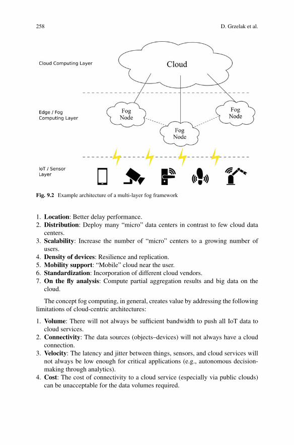
258 D. Grzelak et al.
Fig. 9.2 Example architecture of a multi-layer fog framework
1. Location: Better delay performance.2. Distribution: Deploy many “micro” data centers in contrast to few cloud data
centers.3. Scalability: Increase the number of “micro” centers to a growing number of
users.4. Density of devices: Resilience and replication.5. Mobility support: “Mobile” cloud near the user.6. Standardization: Incorporation of different cloud vendors.7. On the fly analysis: Compute partial aggregation results and big data on the
cloud.
The concept fog computing, in general, creates value by addressing the followinglimitations of cloud-centric architectures:
1. Volume: There will not always be sufficient bandwidth to push all IoT data tocloud services.
2. Connectivity: The data sources (objects–devices) will not always have a cloudconnection.
3. Velocity: The latency and jitter between things, sensors, and cloud services willnot always be low enough for critical applications (e.g., autonomous decision-making through analytics).
4. Cost: The cost of connectivity to a cloud service (especially via public clouds)can be unacceptable for the data volumes required.
9 A Software Toolkit for Complex Sensor Systems in Fog Environments 259
5. Security: For some system owners, it will not be appropriate (because of privacyor security concerns) to push operational data to a cloud service.
6. Interoperability: Peer-to-peer device is often preferred or required for cloudinteroperability for latency, security, risk, or distributed computing reasons.
9.2.2 Sensor Integration
A sensor must be physically and logically integrated into an IoT system. Thecommunication can either be wired or wireless. In both cases, different combina-tions of communication protocols across the ISO-OSI layers exist (e.g., I2C, CAN,TCP, UDP). Depending on the available interfaces and protocols, the embeddedsoftware must provide software components for establishing a connection to theindividual sensor. Once the system can connect sensors, other new challengescomprise the storage and efficient sensor data processing. The STK provides astandard component model for sensor integration, sensor data collection, sensor datafusion, and sensor data analysis. The aim is to overcome the problems above as wellas to build a system with re-usable components.
9.2.2.1 Data Collection
The collection of sensor data encompasses the transient collection and storage ofsensed data. Transient storage is usually formed by a set of triple of parameters(Sensor–Time–Data). In which, Sensor indicates the information of the correspond-ing sensor, Time specifies time information, and Data is the payload of the sensordata. Depending on the available storage and computational performance of adevice, it can only store the captured data for a limited time.
9.2.2.2 Data Fusion
Sensor data fusion is the process of integrating data from multi-sensors to producemore accurate and useful information. Many contextual facts of interest cannot bedetermined by using only one type of sensor. A typical example is depth informationthat is only specified by the difference between two stereoscopically aligned RGB-cameras. In order to acquire the depth information, the data streams of both camerashave to be synchronized and combined. The implementation of sensor data fusionsolutions on IoSense STK is one of the main goals.
260 D. Grzelak et al.
9.2.2.3 Data Analysis
IoT systems use sensor data to provide their services and adapt themselves accord-ing to changing conditions. Sensors are essential to measure the environmentalstate and provide accessible services from software backend. Sensor data analysis isperformed on sensor data by using inspection, transformation, and modeling toolsto discover useful information as well as support decision-making.
9.3 Reference Architecture
The following section introduces the detailed concepts of the IoSense STK. Wedescribe the reference architecture and breaking it down into the various compo-nents of fog including orchestration, distribution and communication and what arethe applicable building blocks in an architectural perspective.
9.3.1 System Infrastructure
A high-level overview of STK and its architecture are depicted in Fig. 9.3. The STKaims to create a software ecosystem, also, providing the core functionalities forsensor integration and communication. The STK also defines interfaces that devel-opers can use to program their app (e.g., application) using the core functionalityof the platform. In this way, the app can connect with the STK directly through theinterfaces.
Furthermore, it may contain new functionalities (i.e., Value Added Functionality)for processing specific tasks. The STK is also designed to integrate easily into otherframeworks. Therefore, the flexibility of the STK is one of the most consideredadvantages.
Inspired by the openHAB architecture, the STK also uses OSGi as a coreframework. Each bundle is a service which is developed separately. It runsindependently or communicates with other bundles to carry out a specific task.Therefore, services can have dependencies on other services allowing them torequest additional functionality among themselves.
Figure 9.4 shows the software architecture of the STK and various open-sourcecomponents it exploits. The open-source software platforms are described briefly inTable 9.1. A service (we use the term “service” for an OSGi bundle) is a componentwhich provides a specific functionality of STK such as data analysis, data process-ing, or connector functionality. The design of a bundle is developed by using thewell-known Concierge open-source software that is based on OSGi model R5 (seeTable 9.1). Either they are deployed on fog nodes or fog nodes can communicatewith services through well-defined interfaces (see Fig. 9.3). This even allows low-end devices that do not support this service architecture due to resource constraint
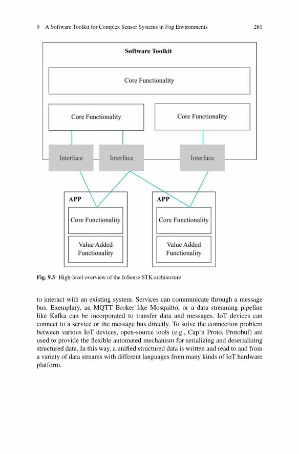
9 A Software Toolkit for Complex Sensor Systems in Fog Environments 261
Fig. 9.3 High-level overview of the IoSense STK architecture
to interact with an existing system. Services can communicate through a messagebus. Exemplary, an MQTT Broker like Mosquitto, or a data streaming pipelinelike Kafka can be incorporated to transfer data and messages. IoT devices canconnect to a service or the message bus directly. To solve the connection problembetween various IoT devices, open-source tools (e.g., Cap’n Proto, Protobuf) areused to provide the flexible automated mechanism for serializing and deserializingstructured data. In this way, a unified structured data is written and read to and froma variety of data streams with different languages from many kinds of IoT hardwareplatform.
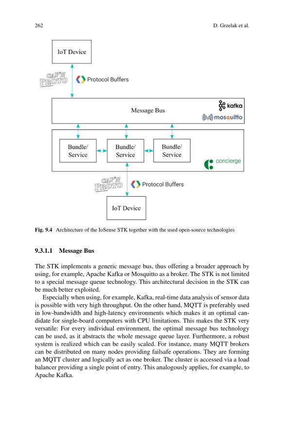
262 D. Grzelak et al.
Fig. 9.4 Architecture of the IoSense STK together with the used open-source technologies
9.3.1.1 Message Bus
The STK implements a generic message bus, thus offering a broader approach byusing, for example, Apache Kafka or Mosquitto as a broker. The STK is not limitedto a special message queue technology. This architectural decision in the STK canbe much better exploited.
Especially when using, for example, Kafka, real-time data analysis of sensor datais possible with very high throughput. On the other hand, MQTT is preferably usedin low-bandwidth and high-latency environments which makes it an optimal can-didate for single-board computers with CPU limitations. This makes the STK veryversatile: For every individual environment, the optimal message bus technologycan be used, as it abstracts the whole message queue layer. Furthermore, a robustsystem is realized which can be easily scaled. For instance, many MQTT brokerscan be distributed on many nodes providing failsafe operations. They are formingan MQTT cluster and logically act as one broker. The cluster is accessed via a loadbalancer providing a single point of entry. This analogously applies, for example, toApache Kafka.
9 A Software Toolkit for Complex Sensor Systems in Fog Environments 263
Table 9.1 Open-source frameworks used by IoSense STK
Name Description
Kafka Apache Kafka is a distributed streaming platform. It is used for buildingreal-time data pipelines and streaming apps. Kafka provides low-latency,high-throughput, fault-tolerant publish and subscribe pipelines. It can processstreams of events. (https://kafka.apache.org/)
Mosquitto Eclipse Mosquitto is an open-source message broker based on the MQTTprotocol. It is designed to guarantee a lightweight specification. Therefore,Mosquitto is suitable for all devices from low power devices to full servers.(https://mosquitto.org/)
Concierge OSGi is a popular framework for dynamic modules for the Java language.Eclipse Concierge provides a small and lightweight implementation optimizedfor mobile, embedded systems and especially IoT. (https://www.eclipse.org/concierge/)
Protobuf Protobuf uses an open-source license and is patent-free, well-tested (used byGoogle since 2001) and language-independent as well as platform-neutral.Protocol buffers (short for Protobuf) are a method of serializing structured data,established by Google. Protobuf provides a code generator for multiplelanguages under an open-source license. It is useful in developing programs tocommunicate with each other over a wire or for storing data. (https://developers.google.com/protocol-buffers/)
Cap’n Proto Cap’n Proto is a lightweight framework and provides a fast data interchangeformat. Also, it also supports a capability-based RPC system with betterperformance compared to traditional RPC. (https://capnproto.org/)
9.3.1.2 Connectors
An essential feature of every IoT framework is the ability to connect to sensors,actuators, and other similar devices. In openHAB, the notion of sensor bindingsis used which is completely different from the STK’s way to interact with suchsensors.
The core questions are: What kind of protocol is used in the device and what kindof data format is used for exchange? Moreover, there are many ways how data can betransferred. The STK abstracts from these details and uses, for example, Google’sProtobuf. This technology makes it very easy to transfer data from different devicesinto the STK and then to other components through the message bus.
Usually, data processing is performed on fog nodes which improves the overallapplication performance when the computation is done locally directly on the fogdevices where the data is produced, or actuators must be executed. Thus, minimizinglatency and shrink response-time.
The communication of the bundle for the distributed processing is carriedout over the generic message bus, as described in the previous section, SectionMessage Bus. The abstract message bus layer is capable of handling differentimplementation of message queue technologies and different data format for theinformation exchange of sensor and actuator data as well.
264 D. Grzelak et al.
The STK is not limited to a single message format technology when connectingsensors. However, for a running application built with the STK, it must be priordefined which data interchange format is facilitated. Usually, any data format canbe used, e.g., JSON or XML. However, as consistency is preferred over mixedformats, the STK already utilizes existing message formats, like Cap’n Proto,Google Protobuf, or Apache Avro which can be used according to the actualimplementation requirements. These message formats have well-defined notationsto define datatypes, protocols and offer serialization and deserialization mechanismfor the data, thus, providing a consistent format across the whole application. Inthe following, the integration of Protobuf is illustrated to demonstrate the STK’scapabilities.
Protobuf is very lightweight, and one of its properties is its efficient encodingwhich allows faster transmissions through a network. This is valuable regarding low-bandwidth and high-latency environments. Also, it is well suited for single-boardcomputers and other devices that have limited CPU, memory, and bandwidth, butit can also be used in large-scale applications. Reading arbitrary sensor informationrequires to define the structure of the Protobuf messages by plain text files before.Those files are then compiled using the Protobuf compiler. After the compilationprocess, the data accessors are automatically generated, as well as simple accessorsto read and write fields, methods to serialize and deserialize structures from andto raw bytes. This is the basic workflow when working with Protobuf, which isvery well integrated into the STK. Since the STK provides an abstract layer forconnecting sensors and other IoT devices, an implementation based on the Cap’nProto data interchange format and Apache Avro support are provided.
9.3.1.3 Bundle Architecture
The STK uses concierge [4] as a lightweight version of the OSGi framework.This makes it preferably in IoT environments. In contrast, openHAB uses Equinox(http://www.eclipse.org/equinox/) as a reference implementation of the OSGi Core4.x specification. Both frameworks, the STK and openHAB, offer the key featuresof OSGi, including modularity through the bundle concept, runtime dynamics formanaging components at runtime and the possibility of inter-component commu-nication through services. To explain, functionality can be easily maintained andextended on-demand. Thus, the flexibility and scalability are guaranteed.
The STK applies the MAPE-K [5] reference model inside a bundle to model anautonomous system with decentralized components.
Figure 9.5 shows the complete detailed architecture of a service. Input data fromthe message bus is received first and then deserialized by the deserializer module.Here, any message format can be used, e.g., Protobuf (see Table 9.1). The corefunctionality of a service is the data processing which is realized by four steps:Monitor, Analyze, Plan, and Execute, finally generating output data. The servicearchitecture conforms to the MAPE-K [5] feedback loop, a widely applied referencecontrol model used for self-adapting systems. After that, the output data combined
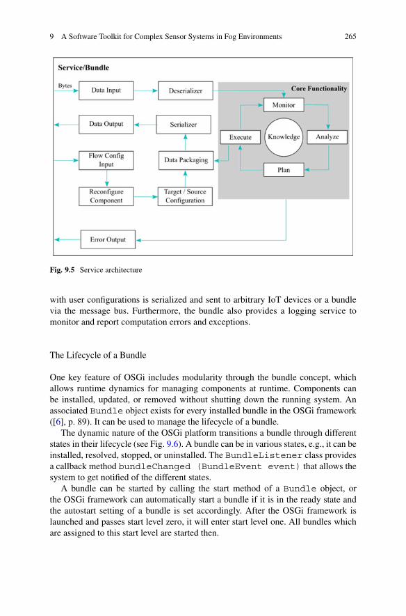
9 A Software Toolkit for Complex Sensor Systems in Fog Environments 265
Fig. 9.5 Service architecture
with user configurations is serialized and sent to arbitrary IoT devices or a bundlevia the message bus. Furthermore, the bundle also provides a logging service tomonitor and report computation errors and exceptions.
The Lifecycle of a Bundle
One key feature of OSGi includes modularity through the bundle concept, whichallows runtime dynamics for managing components at runtime. Components canbe installed, updated, or removed without shutting down the running system. Anassociated Bundle object exists for every installed bundle in the OSGi framework([6], p. 89). It can be used to manage the lifecycle of a bundle.
The dynamic nature of the OSGi platform transitions a bundle through differentstates in their lifecycle (see Fig. 9.6). A bundle can be in various states, e.g., it can beinstalled, resolved, stopped, or uninstalled. The BundleListener class providesa callback method bundleChanged (BundleEvent event) that allows thesystem to get notified of the different states.
A bundle can be started by calling the start method of a Bundle object, orthe OSGi framework can automatically start a bundle if it is in the ready state andthe autostart setting of a bundle is set accordingly. After the OSGi framework islaunched and passes start level zero, it will enter start level one. All bundles whichare assigned to this start level are started then.
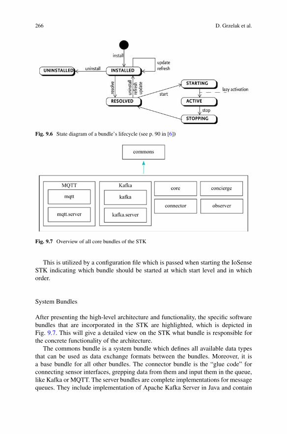
266 D. Grzelak et al.
Fig. 9.6 State diagram of a bundle’s lifecycle (see p. 90 in [6])
Fig. 9.7 Overview of all core bundles of the STK
This is utilized by a configuration file which is passed when starting the IoSenseSTK indicating which bundle should be started at which start level and in whichorder.
System Bundles
After presenting the high-level architecture and functionality, the specific softwarebundles that are incorporated in the STK are highlighted, which is depicted inFig. 9.7. This will give a detailed view on the STK what bundle is responsible forthe concrete functionality of the architecture.
The commons bundle is a system bundle which defines all available data typesthat can be used as data exchange formats between the bundles. Moreover, it isa base bundle for all other bundles. The connector bundle is the “glue code” forconnecting sensor interfaces, grepping data from them and input them in the queue,like Kafka or MQTT. The server bundles are complete implementations for messagequeues. They include implementation of Apache Kafka Server in Java and contain

9 A Software Toolkit for Complex Sensor Systems in Fog Environments 267
an internal implementation of the Mosquitto broker, respectively. The MQTT bundlecan be launched if no external MQTT broker is present. In the observer bundle, thecommon observer pattern is implemented for the STK. This package is optional,but it can be used for tasks, where it is important to listen to a specific number ofconnected sensor types and print them to the console only for visualization. Theconcierge bundle manages the complete lifecycle and holds all configuration files,for instance, which bundles should be loaded and when. The bundle is responsiblefor starting the OSGi framework. The core bundle is an empty module that can beused to include functionality to provide the algorithms throughout all bundles.
Bundle Composition
A configuration file defines the order in which the services are started. This isregarded as the first level of bundle orchestration of an application. This file is passedas program argument to an STK application.
Depending on the actual requirements, the services are deployed on differentdevices. The interaction and communication of the services are carried out over themessage bus. Thus, services can make requests to other services in their currentsystem boundary among themselves in order to execute certain functionalitiesprovided by these services. The problem here is that OSGi bundles are bound tothe scope in their currently running JVM.
Therefore, a distribution of services across all devices that depend on eachother in the fog network is performed. Single bundles are deployed on-demandwhich enables services to request dependencies from remote devices as if they wererunning in the same JVM. Services can be deployed and run on devices dependingon the device’s performance and locality in the fog computing environment.Meaning that the deployment of a service on a device near the physical locationwhere the action takes place (e.g., actuator movement of a robotic arm). Therefore,increasing the execution speed through short network runtimes and decreasednetwork delay.
9.3.2 Fog Computing Application
Being able to harmonize the elements regarding communication and self-adaptionis the key element of a fog computing framework. Thus, after having detailed theinner workings of the architecture, this section introduces how the STK and itscomponents are deployed in the fog.
An application inside the STK comprises a set of so-called bundles, where eachbundle defines a specific set of functions and is regarded as a component. Hence, theapplication itself can be divided into small separate components. A fully workingapplication can run on a single device or can operate as an application, which willpull the necessary bundles from other devices to perform a task.
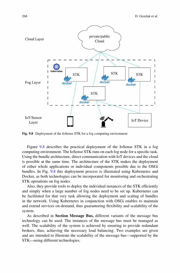
268 D. Grzelak et al.
Fig. 9.8 Deployment of the IoSense STK for a fog computing environment
Figure 9.8 describes the practical deployment of the IoSense STK in a fogcomputing environment. The IoSense STK runs on each fog node for a specific task.Using the bundle architecture, direct communication with IoT devices and the cloudis possible at the same time. The architecture of the STK makes the deploymentof either whole applications or individual components possible due to the OSGibundles. In Fig. 9.8 this deployment process is illustrated using Kubernetes andDocker, as both technologies can be incorporated for monitoring and orchestratingSTK operations on fog nodes.
Also, they provide tools to deploy the individual instances of the STK efficientlyand simply when a large number of fog nodes need to be set up. Kubernetes canbe facilitated for that very task allowing the deployment and scaling of bundlesin the network. Using Kubernetes in conjunction with OSGi enables to maintainand extend services on-demand, thus guaranteeing flexibility and scalability of thesystem.
As described in Section Message Bus, different variants of the message bustechnology can be used. The instances of the message bus must be managed aswell. The scalability of the system is achieved by ensuring to provide redundantbrokers, thus, achieving the necessary load balancing. Two examples are givenand are intended to illustrate the scalability of the message bus—supported by theSTK—using different technologies.
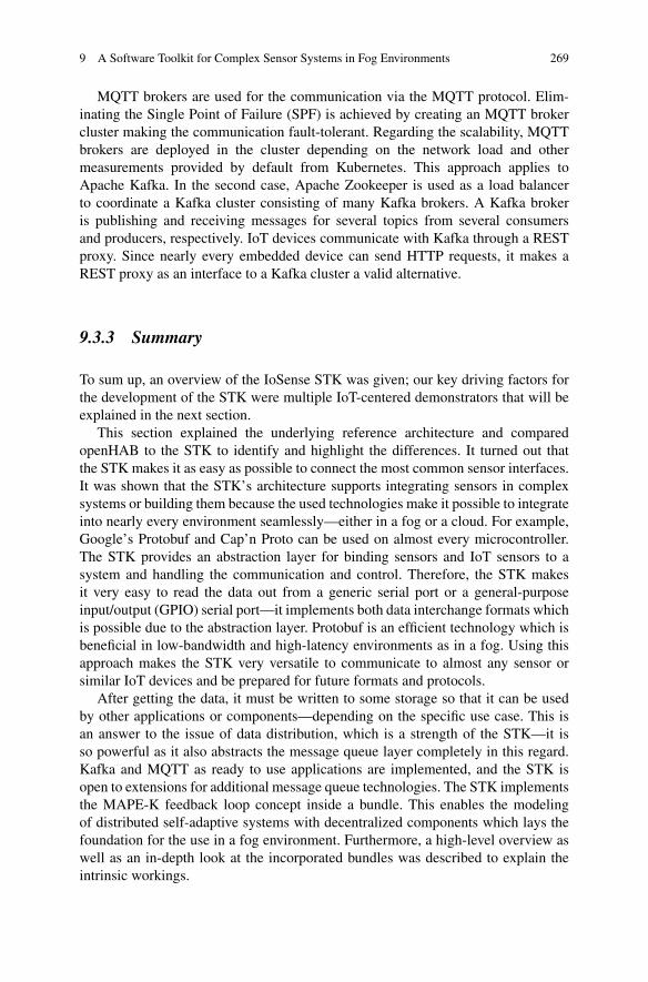
9 A Software Toolkit for Complex Sensor Systems in Fog Environments 269
MQTT brokers are used for the communication via the MQTT protocol. Elim-inating the Single Point of Failure (SPF) is achieved by creating an MQTT brokercluster making the communication fault-tolerant. Regarding the scalability, MQTTbrokers are deployed in the cluster depending on the network load and othermeasurements provided by default from Kubernetes. This approach applies toApache Kafka. In the second case, Apache Zookeeper is used as a load balancerto coordinate a Kafka cluster consisting of many Kafka brokers. A Kafka brokeris publishing and receiving messages for several topics from several consumersand producers, respectively. IoT devices communicate with Kafka through a RESTproxy. Since nearly every embedded device can send HTTP requests, it makes aREST proxy as an interface to a Kafka cluster a valid alternative.
9.3.3 Summary
To sum up, an overview of the IoSense STK was given; our key driving factors forthe development of the STK were multiple IoT-centered demonstrators that will beexplained in the next section.
This section explained the underlying reference architecture and comparedopenHAB to the STK to identify and highlight the differences. It turned out thatthe STK makes it as easy as possible to connect the most common sensor interfaces.It was shown that the STK’s architecture supports integrating sensors in complexsystems or building them because the used technologies make it possible to integrateinto nearly every environment seamlessly—either in a fog or a cloud. For example,Google’s Protobuf and Cap’n Proto can be used on almost every microcontroller.The STK provides an abstraction layer for binding sensors and IoT sensors to asystem and handling the communication and control. Therefore, the STK makesit very easy to read the data out from a generic serial port or a general-purposeinput/output (GPIO) serial port—it implements both data interchange formats whichis possible due to the abstraction layer. Protobuf is an efficient technology which isbeneficial in low-bandwidth and high-latency environments as in a fog. Using thisapproach makes the STK very versatile to communicate to almost any sensor orsimilar IoT devices and be prepared for future formats and protocols.
After getting the data, it must be written to some storage so that it can be usedby other applications or components—depending on the specific use case. This isan answer to the issue of data distribution, which is a strength of the STK—it isso powerful as it also abstracts the message queue layer completely in this regard.Kafka and MQTT as ready to use applications are implemented, and the STK isopen to extensions for additional message queue technologies. The STK implementsthe MAPE-K feedback loop concept inside a bundle. This enables the modelingof distributed self-adaptive systems with decentralized components which lays thefoundation for the use in a fog environment. Furthermore, a high-level overview aswell as an in-depth look at the incorporated bundles was described to explain theintrinsic workings.
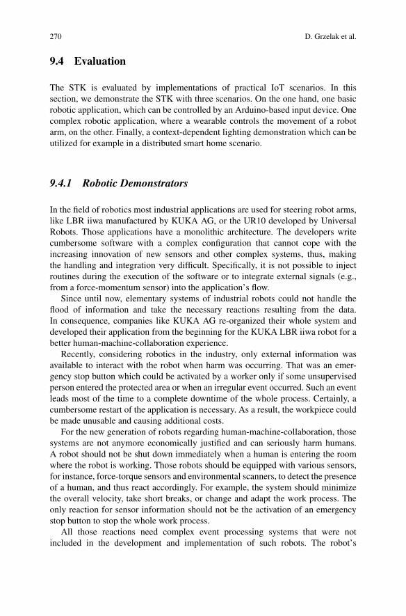
270 D. Grzelak et al.
9.4 Evaluation
The STK is evaluated by implementations of practical IoT scenarios. In thissection, we demonstrate the STK with three scenarios. On the one hand, one basicrobotic application, which can be controlled by an Arduino-based input device. Onecomplex robotic application, where a wearable controls the movement of a robotarm, on the other. Finally, a context-dependent lighting demonstration which can beutilized for example in a distributed smart home scenario.
9.4.1 Robotic Demonstrators
In the field of robotics most industrial applications are used for steering robot arms,like LBR iiwa manufactured by KUKA AG, or the UR10 developed by UniversalRobots. Those applications have a monolithic architecture. The developers writecumbersome software with a complex configuration that cannot cope with theincreasing innovation of new sensors and other complex systems, thus, makingthe handling and integration very difficult. Specifically, it is not possible to injectroutines during the execution of the software or to integrate external signals (e.g.,from a force-momentum sensor) into the application’s flow.
Since until now, elementary systems of industrial robots could not handle theflood of information and take the necessary reactions resulting from the data.In consequence, companies like KUKA AG re-organized their whole system anddeveloped their application from the beginning for the KUKA LBR iiwa robot for abetter human-machine-collaboration experience.
Recently, considering robotics in the industry, only external information wasavailable to interact with the robot when harm was occurring. That was an emer-gency stop button which could be activated by a worker only if some unsupervisedperson entered the protected area or when an irregular event occurred. Such an eventleads most of the time to a complete downtime of the whole process. Certainly, acumbersome restart of the application is necessary. As a result, the workpiece couldbe made unusable and causing additional costs.
For the new generation of robots regarding human-machine-collaboration, thosesystems are not anymore economically justified and can seriously harm humans.A robot should not be shut down immediately when a human is entering the roomwhere the robot is working. Those robots should be equipped with various sensors,for instance, force-torque sensors and environmental scanners, to detect the presenceof a human, and thus react accordingly. For example, the system should minimizethe overall velocity, take short breaks, or change and adapt the work process. Theonly reaction for sensor information should not be the activation of an emergencystop button to stop the whole work process.
All those reactions need complex event processing systems that were notincluded in the development and implementation of such robots. The robot’s
9 A Software Toolkit for Complex Sensor Systems in Fog Environments 271
adaption of the work process with multiple collaborating human workers is a furtherarea. Without a doubt, every human has different body proportions which make theadaption of the robot necessary.
Specifically, KUKA AG was taking this event processing approach with theirSunrise-OS. A robot arm gets different events from other robots which can beprocessed in parallel, and therefore react accordingly and adapt automaticallyat execution time/runtime of the system. This implementation approach is veryappropriate for the above-mentioned use case. One drawback still exists: thissolution is not scalable with increasing sensors, as in other areas like currentlyevolving for smart homes. Therefore, different approaches are indeed necessary—where the STK is one of those.
9.4.1.1 Controlling a Robotic Arm with a 3D Mouse
For the first evaluation, a three-dimensional mouse is implemented to control anythree-link robot with revolute joints. An arbitrary IoT device is utilized to steera robotic arm. This first example demonstrates some basic features of the STKregarding the deployment of single services on different devices and how theseservices communicate through a message bus.
The robot we used here is a UR10, produced by Universal Robots. The inputcontroller representing the three-dimensional mouse is described in a moment. Theinput controller generates the necessary data that is generated by the motions andtransmits it to the robot, finally, reproducing the results of the received data byimitating the motion of the controller. This process is depicted in Fig. 9.9.
Fig. 9.9 The translation of the input controller (that is, the cube symbol) from a frame A to frameB results in x which is translated to x′. The input controller’s position corresponds to the endeffector orientation
272 D. Grzelak et al.
In the figure two frames A and B are shown; between these two frames, amotion of the controller is executed resulting in a change, denoted by Δx. Severalsteps including mapping, transformation, and inverse kinematics computation areperformed to get the corresponding Δx
′for the robot manipulator which changes the
position of the end effector E accordingly. This change represents the same motionas performed with the controller.
Input Controller
The controller is regarded as a three-dimensional mouse, intended to be held byone hand. It has the form of a cube where the housing is made from cardboardwith a dimension of 100 mm × 100 mm × 100 mm (H × W × D). A Feather M0from Adafruit is used as portable microcontroller board with an ATSAMD21G18processor running at 48 MHz with 3.3 V power. Connected to the Feather M0 is theBNO055, a 9-DOF sensor to acquire the necessary orientation value along two axes,and additionally it is used to measure the displacement with respect to the device’sinitial position. The sensors deliver orientation information and acceleration datawhich are used to build the spatial vector representing the current position of thisinput controller.
Service Components
Software bundles contain certain parts of the whole functionality. These bundles aredistributed on different fog nodes in the local network allowing the local processingnear the devices producing the data or actuators, thus connecting the fog and IoTlayer.
First, the input controller sends data using a client to communicate viaMQTT. Therefore, we created the MQTT topics o/orientation ando/acceleration to send the angles and acceleration values of the inputcontroller, respectively. After the broker receives the message, it sends it to theConnector bundle. The data format for the transmission is specified using Google’sProtocol Buffers Format. We defined two message formats, on the one hand for theorientation data, on the other for the acceleration. Each message contains the currentstate of the input controller for a single time step. The message for the orientationcontains angle values for all three axes, a “face” property (indicating the upwardspointed face, perpendicular to the floor), and a 3-tupel for time attributes storing thesending, receiving, and processing time. The message format for the accelerationdata of the controller gathered by the BNO055 is defined analogously to theorientation message format. MQTT is used to transmit the data to the Connectorbundle for further processing.
Secondly, as the Connector receives the data packages, it sends these to theAnalyzer. Before, the connector validates the data and performs some initial pre-processing. The Analyzer bundle contains the whole functionality of the motiontranslation process which includes value mapping, coordinate system transforma-
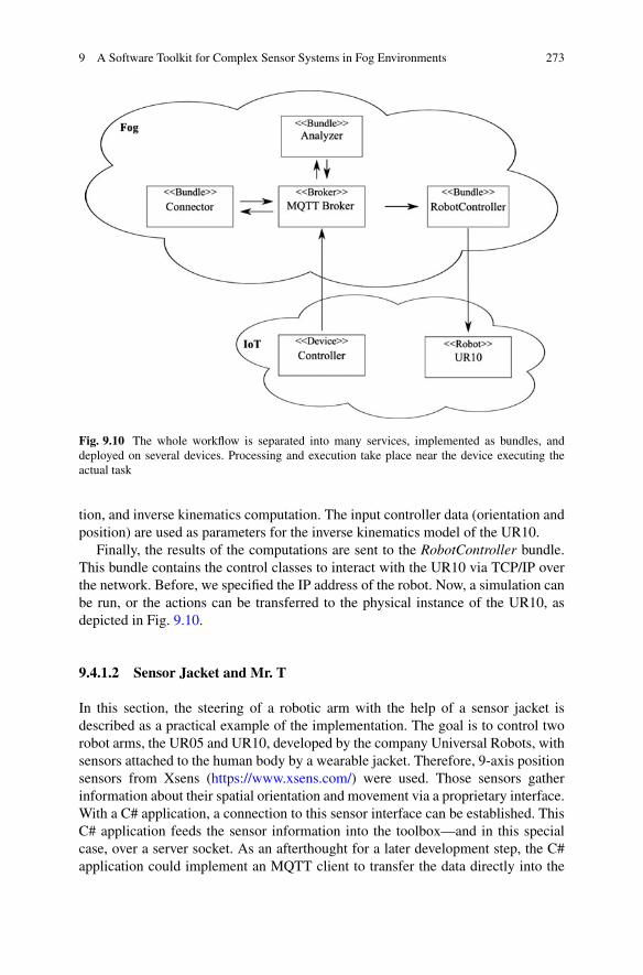
9 A Software Toolkit for Complex Sensor Systems in Fog Environments 273
Fig. 9.10 The whole workflow is separated into many services, implemented as bundles, anddeployed on several devices. Processing and execution take place near the device executing theactual task
tion, and inverse kinematics computation. The input controller data (orientation andposition) are used as parameters for the inverse kinematics model of the UR10.
Finally, the results of the computations are sent to the RobotController bundle.This bundle contains the control classes to interact with the UR10 via TCP/IP overthe network. Before, we specified the IP address of the robot. Now, a simulation canbe run, or the actions can be transferred to the physical instance of the UR10, asdepicted in Fig. 9.10.
9.4.1.2 Sensor Jacket and Mr. T
In this section, the steering of a robotic arm with the help of a sensor jacket isdescribed as a practical example of the implementation. The goal is to control tworobot arms, the UR05 and UR10, developed by the company Universal Robots, withsensors attached to the human body by a wearable jacket. Therefore, 9-axis positionsensors from Xsens (https://www.xsens.com/) were used. Those sensors gatherinformation about their spatial orientation and movement via a proprietary interface.With a C# application, a connection to this sensor interface can be established. ThisC# application feeds the sensor information into the toolbox—and in this specialcase, over a server socket. As an afterthought for a later development step, the C#application could implement an MQTT client to transfer the data directly into the
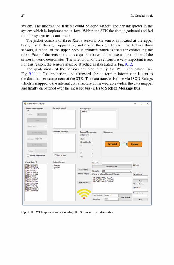
274 D. Grzelak et al.
system. The information transfer could be done without another interpreter in thesystem which is implemented in Java. Within the STK the data is gathered and fedinto the system as a data stream.
The jacket consists of three Xsens sensors: one sensor is located at the upperbody, one at the right upper arm, and one at the right forearm. With these threesensors, a model of the upper body is spanned which is used for controlling therobot. Each of the sensors outputs a quaternion which represents the rotation of thesensor in world coordinates. The orientation of the sensors is a very important issue.For this reason, the sensors must be attached as illustrated in Fig. 9.12.
The quaternions of the sensors are read out by the WPF application (seeFig. 9.11), a C# application, and afterward, the quaternion information is sent tothe data mapper component of the STK. The data transfer is done via JSON-Stringswhich is mapped to the internal data structure of the wearable within the data mapperand finally dispatched over the message bus (refer to Section Message Bus).
Fig. 9.11 WPF application for reading the Xsens sensor information
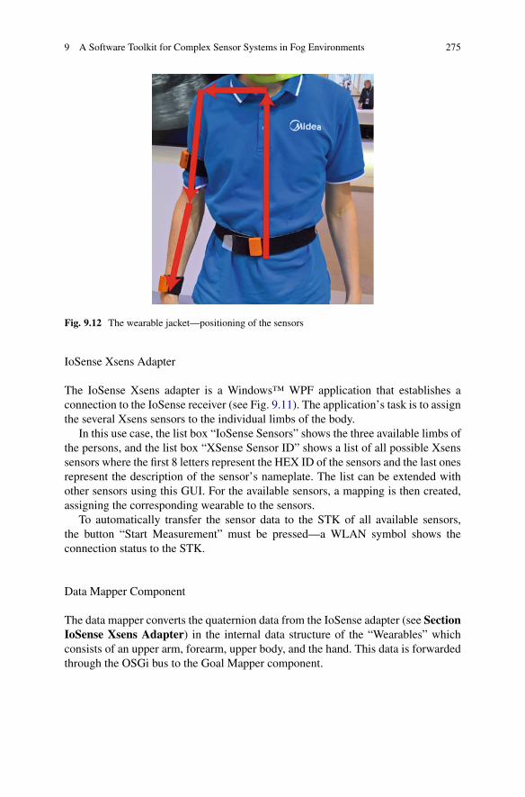
9 A Software Toolkit for Complex Sensor Systems in Fog Environments 275
Fig. 9.12 The wearable jacket—positioning of the sensors
IoSense Xsens Adapter
The IoSense Xsens adapter is a Windows™ WPF application that establishes aconnection to the IoSense receiver (see Fig. 9.11). The application’s task is to assignthe several Xsens sensors to the individual limbs of the body.
In this use case, the list box “IoSense Sensors” shows the three available limbs ofthe persons, and the list box “XSense Sensor ID” shows a list of all possible Xsenssensors where the first 8 letters represent the HEX ID of the sensors and the last onesrepresent the description of the sensor’s nameplate. The list can be extended withother sensors using this GUI. For the available sensors, a mapping is then created,assigning the corresponding wearable to the sensors.
To automatically transfer the sensor data to the STK of all available sensors,the button “Start Measurement” must be pressed—a WLAN symbol shows theconnection status to the STK.
Data Mapper Component
The data mapper converts the quaternion data from the IoSense adapter (see SectionIoSense Xsens Adapter) in the internal data structure of the “Wearables” whichconsists of an upper arm, forearm, upper body, and the hand. This data is forwardedthrough the OSGi bus to the Goal Mapper component.
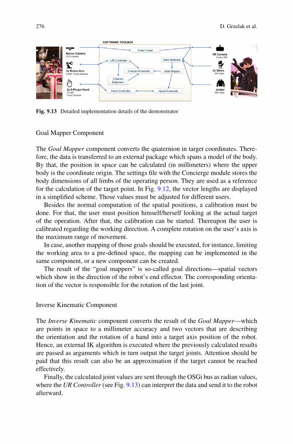
276 D. Grzelak et al.
Fig. 9.13 Detailed implementation details of the demonstrator
Goal Mapper Component
The Goal Mapper component converts the quaternion in target coordinates. There-fore, the data is transferred to an external package which spans a model of the body.By that, the position in space can be calculated (in millimeters) where the upperbody is the coordinate origin. The settings file with the Concierge module stores thebody dimensions of all limbs of the operating person. They are used as a referencefor the calculation of the target point. In Fig. 9.12, the vector lengths are displayedin a simplified scheme. Those values must be adjusted for different users.
Besides the normal computation of the spatial positions, a calibration must bedone. For that, the user must position himself/herself looking at the actual targetof the operation. After that, the calibration can be started. Thereupon the user iscalibrated regarding the working direction. A complete rotation on the user’s axis isthe maximum range of movement.
In case, another mapping of those goals should be executed, for instance, limitingthe working area to a pre-defined space, the mapping can be implemented in thesame component, or a new component can be created.
The result of the “goal mappers” is so-called goal directions—spatial vectorswhich show in the direction of the robot’s end effector. The corresponding orienta-tion of the vector is responsible for the rotation of the last joint.
Inverse Kinematic Component
The Inverse Kinematic component converts the result of the Goal Mapper—whichare points in space to a millimeter accuracy and two vectors that are describingthe orientation and the rotation of a hand into a target axis position of the robot.Hence, an external IK algorithm is executed where the previously calculated resultsare passed as arguments which in turn output the target joints. Attention should bepaid that this result can also be an approximation if the target cannot be reachedeffectively.
Finally, the calculated joint values are sent through the OSGi bus as radian values,where the UR Controller (see Fig. 9.13) can interpret the data and send it to the robotafterward.
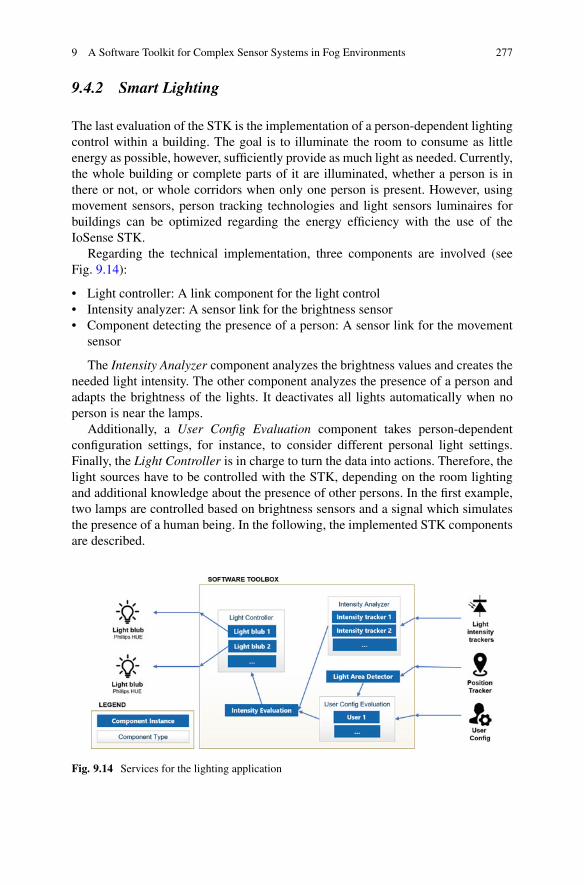
9 A Software Toolkit for Complex Sensor Systems in Fog Environments 277
9.4.2 Smart Lighting
The last evaluation of the STK is the implementation of a person-dependent lightingcontrol within a building. The goal is to illuminate the room to consume as littleenergy as possible, however, sufficiently provide as much light as needed. Currently,the whole building or complete parts of it are illuminated, whether a person is inthere or not, or whole corridors when only one person is present. However, usingmovement sensors, person tracking technologies and light sensors luminaires forbuildings can be optimized regarding the energy efficiency with the use of theIoSense STK.
Regarding the technical implementation, three components are involved (seeFig. 9.14):
• Light controller: A link component for the light control• Intensity analyzer: A sensor link for the brightness sensor• Component detecting the presence of a person: A sensor link for the movement
sensor
The Intensity Analyzer component analyzes the brightness values and creates theneeded light intensity. The other component analyzes the presence of a person andadapts the brightness of the lights. It deactivates all lights automatically when noperson is near the lamps.
Additionally, a User Config Evaluation component takes person-dependentconfiguration settings, for instance, to consider different personal light settings.Finally, the Light Controller is in charge to turn the data into actions. Therefore, thelight sources have to be controlled with the STK, depending on the room lightingand additional knowledge about the presence of other persons. In the first example,two lamps are controlled based on brightness sensors and a signal which simulatesthe presence of a human being. In the following, the implemented STK componentsare described.
Fig. 9.14 Services for the lighting application
278 D. Grzelak et al.
The STK allows getting the different information from all those IoT sensordevices to implement a self-adapting light control system, considering the userpreferences.
9.4.3 Summary
This section presented the various IoSense demonstrators and how they contributedto the final stage of the STK’s implementation. The different use cases were keydriving factors in the development of the STK.
Controlling a robot with the use of a sensor jacket is a demanding andsophisticated use case which was implemented with the Mr. T demonstrator. Itsolves limitations regarding real-time capabilities. The 3D mouse had shown analternative approach of steering a robot arm. The STK was used to develop a robustreal-time system suitable for this scenario within fog computing environments.
Extending the application spectrum even further, another demonstrator in thefield of smart homes was developed. The Smart Light demonstrator implemented aperson-dependent illumination control system.
9.5 Related Work
Within the last years, several software systems were proposed to tackle the newchallenges from the IoT. These systems range from full-fledged solutions for smarthome over research prototypes, which only focus on a few concerns. Our proposedSTK can be seen as an architectural foundation to all of these. While we do notdeliver specific sensor implementations, we proposed an architecture which can beadjusted to fit most scenarios.
One of the most famous frameworks in the area of home automation, whichhas a large community and supports many protocols, is the openHAB (OpenHome Automation Bus, https://www.openhab.org/) middleware. All components ofopenHAB are shown in Fig. 9.15.
OpenHAB is based on OSGi that is a Java framework for developing anddeploying modular software programs and libraries. Each OSGi bundle is dedicatedto a specific purpose in openHAB. A detailed explanation can be found in [8]. Byexploiting OSGi, openHAB can easily maintain and extend its functionalities on-demand. Therefore, the flexibility and scalability are guaranteed. For instance, thereare many communication technologies among different IoT ecosystems. To adaptthem to openHAB, it provides the protocol binding feature with core components,such as the Event Bus (see Fig. 9.16) and Binding bundles, to provide the necessarycommunication abilities for different kinds of underlying technologies, shown inFig. 9.16. In openHAB, Bindings integrate small devices, physical hardware, andexternal systems into the system. They are a special type of add-on for openHAB.
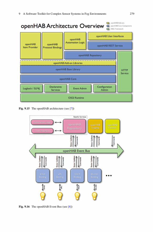
9 A Software Toolkit for Complex Sensor Systems in Fog Environments 279
Fig. 9.15 The openHAB architecture (see [7])
Fig. 9.16 The openHAB Event Bus (see [8])
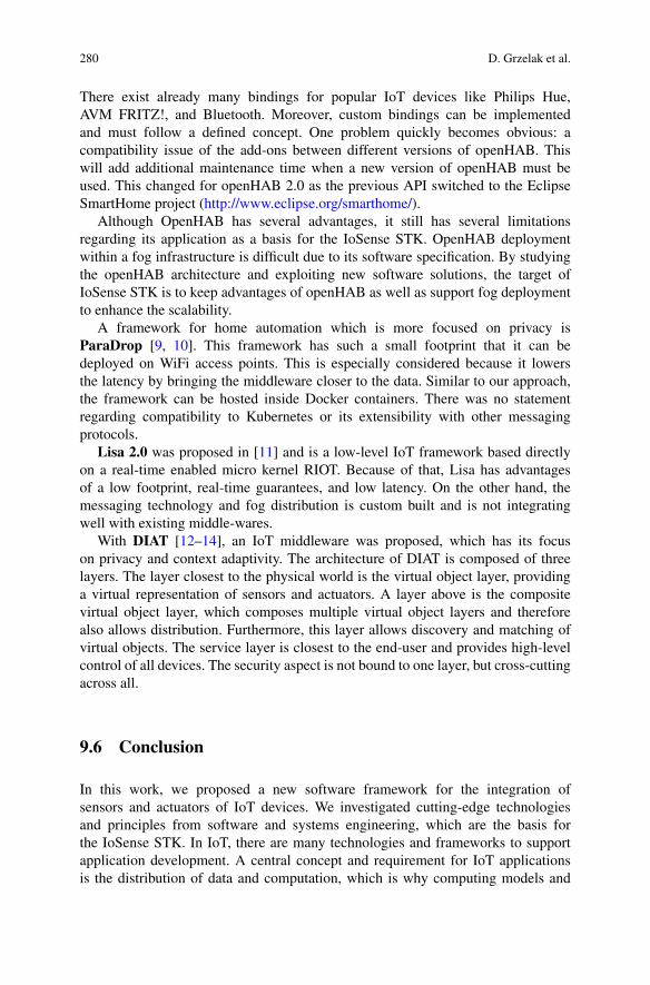
280 D. Grzelak et al.
There exist already many bindings for popular IoT devices like Philips Hue,AVM FRITZ!, and Bluetooth. Moreover, custom bindings can be implementedand must follow a defined concept. One problem quickly becomes obvious: acompatibility issue of the add-ons between different versions of openHAB. Thiswill add additional maintenance time when a new version of openHAB must beused. This changed for openHAB 2.0 as the previous API switched to the EclipseSmartHome project (http://www.eclipse.org/smarthome/).
Although OpenHAB has several advantages, it still has several limitationsregarding its application as a basis for the IoSense STK. OpenHAB deploymentwithin a fog infrastructure is difficult due to its software specification. By studyingthe openHAB architecture and exploiting new software solutions, the target ofIoSense STK is to keep advantages of openHAB as well as support fog deploymentto enhance the scalability.
A framework for home automation which is more focused on privacy isParaDrop [9, 10]. This framework has such a small footprint that it can bedeployed on WiFi access points. This is especially considered because it lowersthe latency by bringing the middleware closer to the data. Similar to our approach,the framework can be hosted inside Docker containers. There was no statementregarding compatibility to Kubernetes or its extensibility with other messagingprotocols.
Lisa 2.0 was proposed in [11] and is a low-level IoT framework based directlyon a real-time enabled micro kernel RIOT. Because of that, Lisa has advantagesof a low footprint, real-time guarantees, and low latency. On the other hand, themessaging technology and fog distribution is custom built and is not integratingwell with existing middle-wares.
With DIAT [12–14], an IoT middleware was proposed, which has its focuson privacy and context adaptivity. The architecture of DIAT is composed of threelayers. The layer closest to the physical world is the virtual object layer, providinga virtual representation of sensors and actuators. A layer above is the compositevirtual object layer, which composes multiple virtual object layers and thereforealso allows distribution. Furthermore, this layer allows discovery and matching ofvirtual objects. The service layer is closest to the end-user and provides high-levelcontrol of all devices. The security aspect is not bound to one layer, but cross-cuttingacross all.
9.6 Conclusion
In this work, we proposed a new software framework for the integration ofsensors and actuators of IoT devices. We investigated cutting-edge technologiesand principles from software and systems engineering, which are the basis forthe IoSense STK. In IoT, there are many technologies and frameworks to supportapplication development. A central concept and requirement for IoT applicationsis the distribution of data and computation, which is why computing models and
9 A Software Toolkit for Complex Sensor Systems in Fog Environments 281
system architectures such as fog computing, cloud computing, edge computing, anddew computing [15] are emerging as new paradigms and becoming more importantin this area. With the STK, we focus on the application of future-proof technologiesand standards.
Within the course of our investigation and evaluation of technologies, frame-works, applications, and architectures related to IoT and sensors with respect totheir advantages and disadvantages to being used within our sensor framework, weidentified various concepts that will form the basis of the IoSense Software Toolkit.The new paradigm of fog computing will serve as the central system architectureprinciple as it fulfills the requirements of fast data processing, achieving low latencyand high bandwidth as well as security and fault-tolerance for sensor applicationsclose to the computing edge with real-time demands. The principle of Bundles,taken from the OSGi standard, permits a component-oriented software develop-ment approach and flexible deployment including runtime updates. The referencearchitecture of an IoT middleware for smart homes described by openHAB showspromising concepts regarding the combination of the aforementioned technologies.We will use this architecture as a basis and guide for our developments (e.g., havingan event bus for communication and adapters to integrate new sensors). To remedythe lack of support for the fog computing infrastructure, we will use state-of-the-art and future-proof containerization and orchestration techniques based on Dockerand Kubernetes.
In our ongoing work, we are combining the system of bundles with formalmethods of Petri nets and context adaptation. With an adaptive Petri net [16],the bundles and its order of execution are configured based on a context (e.g., asensor value). With this, the designed architecture can be verified according to thespecification with temporal logic. Furthermore, we are working on an improveddata handling by combining the STK with the statistics tool R. To cope with thehuge amount of data in our distributed fog architecture, the data handling has to bemanaged in a distributed manner by utilizing R Container [17].
The IoSense STK was evaluated on three use cases, ranging from mediumcomplexity to highly complex robotic applications. They demonstrate how thecomponents of the STK can be utilized and formed in a way that they fit modernIoT-centered projects.
References
1. 50 billion devices online by 2020, https://www.telegraph.co.uk/technology/internet/9051590/50-billion-devices-online-by-2020.html. Accessed 21 Apr 2018
2. F. Bonomi, R. Milito, J. Zhu, S. Addepalli, Fog computing and its role in the internet of things,in Proceedings of the First Edition of the MCC Workshop on Mobile Cloud Computing, pp.13–16. MCC ‘12
3. A. Al-Fuqaha, M. Guizani, M. Mohammadi, M. Aledhari, M. Ayyash, Internet of things: asurvey on enabling technologies, protocols, and applications. IEEE Commun. Surv. Tutor.17(4), 2347–2376 (2015)

282 D. Grzelak et al.
4. Rellermeyer und Alonso, “Concierge”, in Proceedings of the 2nd ACM SIGOPS/EuroSysEuropean Conference on Computer Systems (2007). https://doi.org/10.1145/1272996.1273022
5. “An Architectural Blueprint for Autonomic Computing.”, White Paper, http://www-03.ibm.com/autonomic/pdfs/AC%20Blueprint%20White%20Paper%20V7.pdf. Accessed 9Apr 2018
6. OSGi, “OSGi Core Release 5”, https://osgi.org/download/r5/osgi.core-5.0.0.pdf. Accessed 10Apr 2018
7. https://commons.wikimedia.org/wiki/File:OpenHAB_Architecture.png. Accessed 12 Apr2018
8. “openHAB—empowering the smart home”, http://www.openhab.org/. Accessed 15 Aug 20189. P. Liu, D. Willis, S. Banerjee, Paradrop: enabling lightweight multi-tenancy at the Network’s
extreme edge, in Symposium on Edge Computing (SEC), IEEE/ACM, (2016), pp. 1–1310. D.F. Willis, A. Dasgupta, S. Banerjee, ParaDrop: A multi-tenant platform for dynamically
installed third party services on home gateways, in Proceedings of the 2014 ACM SIGCOMMWorkshop on Distributed Cloud Computing, DCC ‘14, (ACM, New York, 2014), pp. 43–44
11. B. Negash, A.M. Rahmani, T. Westerlund, P. Liljeberg, H. Tenhunen, LISA 2.0: Lightweightinternet of things service bus architecture using node centric networking. J. Ambient. Intell.Humaniz. Comput. 7(3), 305–319 (2016)
12. C. Sarkar, S.N.A.U. Nambi, R.V. Prasad, A. Rahim, R. Neisse, G. Baldini, DIAT: A scalabledistributed architecture for IoT. IEEE Internet Things J. 2(3), 230–239 (2015)
13. R. Neisse, I.N. Fovino, G. Baldini, V. Stavroulaki, P. Vlacheas, R. Giaffreda, A model-based security toolkit for the internet of things, in 2014 Ninth International Conference onAvailability, Reliability and Security (ARES), (2014), pp. 78–87
14. P. Vlacheas, R. Giaffreda, V. Stavroulaki, D. Kelaidonis, V. Foteinos, G. Poulios, P. Demes-tichas, A. Somov, A.R. Biswas, K. Moessner, Enabling smart cities through a cognitivemanagement framework for the internet of things. IEEE Commun. Mag. 51(6), 102–111(2013)
15. P.P. Ray, An introduction to dew computing: Definition, concept and implications. IEEE Access6, 723–737 (2018). https://doi.org/10.1109/ACCESS.2017.2775042
16. C. Mai, R. Schöne, J. Mey, T. Kühn, U. Aßmann, Adaptive Petri Nets – A Petri Net Extensionfor Reconfigurable Structures. Presented at the ADAPTIVE 2018, The 10th internationalconference on adaptive and self-adaptive systems and applications, 18 Feb (2018)
17. D. Grzelak, J. Mey, U. Aßmann, Design and concept of an osmotic analytics platform based onR container, in Proceedings of the 2018 International Conference on Foundations of ComputerScience (FCS’18), (CSREA Press, Las Vegas, 2018), pp. 29–35

Chapter 10Sensor System Optimization UnderUncertainty
Wolfgang Granig, Lisa-Marie Faller, and Hubert Zangl
10.1 Introduction
10.1.1 Motivation
Sensor systems are used in a wide range of consumer, industrial, automotive, andaerospace applications. To enable progress in novel application such as autonomoussystems and robotics, e.g., autonomous automotive driving [1, 2] and unmannedautonomous vehicles [3, 4], an increased number of in-built sensors is necessary. Inall those fields, it is essential to define architectures for these sensor systems, whichare optimized concerning performance, operating conditions, size and productioncosts, etc. This chapter focuses on optimization of sensor system architectures,considering uncertainties in input parameters, design parameters, environmentalparameters, and the calibration setup, to achieve given system performance require-ments. When defining sensor system architectures, the goal is to achieve bestpossible performance together with robustness against external influences whilekeeping production and maintenance costs low. The challenge in this step is thelack of exact knowledge of the governing physics of each individual producedsystem (e.g., due to individual production variation effects, etc.) as well as the effectof external influences and deviations to the final system. A common approach isto start from a basic system model based on past experiences and building-blockspecifications. A generic system model for further analysis is shown in Fig. 10.1where the real input value x is project to the estimated value x and its uncertainty
W. Granig (�)Infineon Technologies Austria AG, Villach, Austriae-mail: [email protected]
L.-M. Faller · H. ZanglAlpen-Adria-Universität, Klagenfurt, Austria
© Springer Nature Switzerland AG 2020W. D. van Driel et al. (eds.), Sensor Systems Simulations,https://doi.org/10.1007/978-3-030-16577-2_10
283

284 W. Granig et al.
Fig. 10.1 This figure shows the sensor system model for further analysis and optimizations. Thesensor projects each real input value x into estimated output x. This process is influenced by designparameters S and influencing parameters V as illustrated by the dependencies of the transfer-function h(·). However, as the influencing parameters are random variables, also the output X
becomes a random variable and the actual estimate xis a realization of X
ux influenced by design parameters S and influencing parameters V. Design andinfluencing parameters have nominal values represented in a vector (indicated hereby bold letter), but in the practical realization they have random deviations andconsequently they have to be described by random variables (indicated here bycapital letters) generating the output random variable X.
One common procedure is then to define typical operating conditions of thesystem and to excite the design- and influencing parameters, which are known andconsidered most important, up to their extreme values to assure the fulfillment ofspecifications [5]. Monte-Carlo simulations [6] can be performed if possible, butthis is a time-consuming process, and high numbers of design parameters as well asinfluencing parameters increase the degrees of freedom and consequently lower thechance of finding all possible combinations which would violate the specification.In case a violation is found, and the design has to be changed to overcome the issue,the Monte-Carlo simulations have to be repeated. A reduction of iterations and aso-called pareto-front can be generated in case of multiple optimization objectives[7]. However, this process is only reasonable, if the system model adequatelymodels the real system. Oftentimes, no such model is available during sensor systemarchitectural exploration. The aim of this chapter is to describe a simplified andefficient way for sensor system optimization even in the architecture definitionphase, based on statistical methods.
10.1.2 Statistic Considerations on Measurement Results
Real sensor systems convert the sensor output y, now realizations for randomvariables and depending on influencing parameters and design parameters, to theestimated output variable. This conversion is modeled by mathematical combina-tions of variables and parameters, also termed estimator. A general model is shown
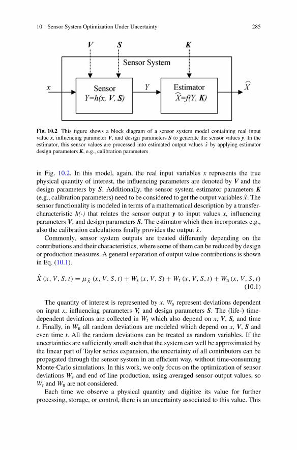
10 Sensor System Optimization Under Uncertainty 285
Fig. 10.2 This figure shows a block diagram of a sensor system model containing real inputvalue x, influencing parameter V, and design parameters S to generate the sensor values y. In theestimator, this sensor values are processed into estimated output values x by applying estimatordesign parameters K, e.g., calibration parameters
in Fig. 10.2. In this model, again, the real input variables x represents the truephysical quantity of interest, the influencing parameters are denoted by V and thedesign parameters by S. Additionally, the sensor system estimator parameters K(e.g., calibration parameters) need to be considered to get the output variables x. Thesensor functionality is modeled in terms of a mathematical description by a transfer-characteristic h(·) that relates the sensor output y to input values x, influencingparameters V, and design parameters S. The estimator which then incorporates e.g.,also the calibration calculations finally provides the output x.
Commonly, sensor system outputs are treated differently depending on thecontributions and their characteristics, where some of them can be reduced by designor production measures. A general separation of output value contributions is shownin Eq. (10.1).
X (x, V , S, t) = μX
(x, V, S, t) + Ws (x, V , S) + Wt (x, V, S, t) + Wn (x, V , S, t)
(10.1)
The quantity of interest is represented by x, Ws represent deviations dependenton input x, influencing parameters V, and design parameters S. The (life-) time-dependent deviations are collected in Wt which also depend on x, V, S, and timet. Finally, in Wn all random deviations are modeled which depend on x, V, S andeven time t. All the random deviations can be treated as random variables. If theuncertainties are sufficiently small such that the system can well be approximated bythe linear part of Taylor series expansion, the uncertainty of all contributors can bepropagated through the sensor system in an efficient way, without time-consumingMonte-Carlo simulations. In this work, we only focus on the optimization of sensordeviations Ws and end of line production, using averaged sensor output values, soWt and Wn are not considered.
Each time we observe a physical quantity and digitize its value for furtherprocessing, storage, or control, there is an uncertainty associated to this value. This
286 W. Granig et al.
is a well-known fact and cannot be fully resolved by improving the measurementprinciple as described in Heisenberg’s famous uncertainty principle. In order toindicate the quality of a measurement result, it is thus common to state themeasured value of physical quantities together with an indication of its uncertainty.Historically, the measurement error was considered in a practical way to describethis quality by means of a measurement deviation. Nowadays, a standardizedrepresentation of uncertain measurement quantities on a statistical basis is definedin the “Guide to the expression of uncertainty in measurements” (GUM) [8] basedon standardized vocabulary to represent uncertain measurement results [9]. On thebasis of the GUM, a standardized way is given to define measurement results in auniversal, internally consistent and transferable way. In this context, a measurementresult for a single unknown quantity has to be associated with its measurementquality expressed in measurement uncertainty, here denoted as standard uncertaintyexpressed as a standard-deviation. This uncertainty can be defined by a so-calledType A evaluation, using statistical analysis of series of observations, or applyinga Type B evaluation other than statistical analysis. Measurement results, in thiscontext, can be described by a set of two parameters with their estimate x andassociated standard uncertainty ux to the true value, see Eq. (10.2).
measurement result = {x, ux
}(10.2)
Practically, when reporting measurement results, the GUM recommends todenote uncertainty in terms of least significant digits given in brackets after theestimated value. For example, for a voltage measurement result of U = 12.371 Vwith an associated standard uncertainty of 15 mV we would write this relationshipacc. Eq. (10.3).
U = 12.371(15) V (10.3)
Such uncertain deviations ux can result from various sources, such as thermalnoise, mechanical stress, quantization-noise, general measurement errors as wellas all other external influences, changing the measurement value. These randomdeviations are not systematically predictable, but for large numbers of measurementresults, like present in mass production, they can be treated as mathematical randomvariable Y and are expressed in probability functions. The cumulative densityfunction (cdf) of this random variable represents the probability of a realizationof Y being smaller than y, expressed in Eq. (10.4).
FY (y) = Pr (Y ≤ y) (10.4)
The probability density function (pdf ) of Y is the derivative of the cumulativedensity function as shown in Eq. (10.5), also written as p(y).
fY (y) = p(y) = FY(y)
dy(10.5)
10 Sensor System Optimization Under Uncertainty 287
The most famous probability density function for random deviations is theGaussian probability density function, or normal distribution function which isdefined as shown in Eq.(10.6). It is also considered for measurement results inthe GUM [8]. There μY represents the expected value or mean value and σ Y thestandard-deviation.
fY(y) = p(y) = 1√2πσY
2· e
− 12
(y−μY
σY
)2
(10.6)
This probability density distribution function is very common because of its reg-ular presence in natural observations, as well as because of the central limit theorem.The central limit theorem [10] tells us that for large number of measurement resultsyn, the distribution of the sums is approximately normal regardless of the form ofthe distribution of the individual measurement results y (see Eq. (10.7)).
limn→∞
Y1 + · · · + Yn − nμY
σ√
n∼ N (0; 1) (10.7)
10.1.3 Specification Limits of Measurement Results
Every sensor system has to transfer the parameter of interest (most of the timelinearly) into a readable value, representing the value of interest. This transfer hasto be performed, fulfilling certain performance requirements, defined as maximumallowed positive and negative deviations from this transfer-characteristic. For furtheranalysis and specifications only, this deviation from the target transfer-characteristicis shown and in focus. This relationship including parameter dependence andallowed minimum and maximum deviations are drawn in Fig. 10.3.
Sensor systems for commercial use have to generate measurement results withdeviations smaller than the maximum positive and larger than the maximumnegative specification value with very high probability. Applying this to a largenumber of sensor systems, and measurement samples, using the information fromthe previous section, expressing deviations as statistical random variables, we geta probability of sensor systems fulfilling these specification limits. An example fortwo different probability density functions including deviations, stating specificationlimits, is shown in Fig. 10.4. Logarithmic scales are used to show the probabilitydensity regions farther from the mean values.
Such systematic deviations can occur in real sensor systems, for example whencompensating a higher order polynomial behavior by a lower order approximation.In sensor system applications, such statistic descriptions are necessary to determinethe probabilities of specification violations, and to specify safe operation regionsfor the respective systems. Additionally, for the designers it can provide valuableinformation to assess if their system will meet requirements in terms of resolution,
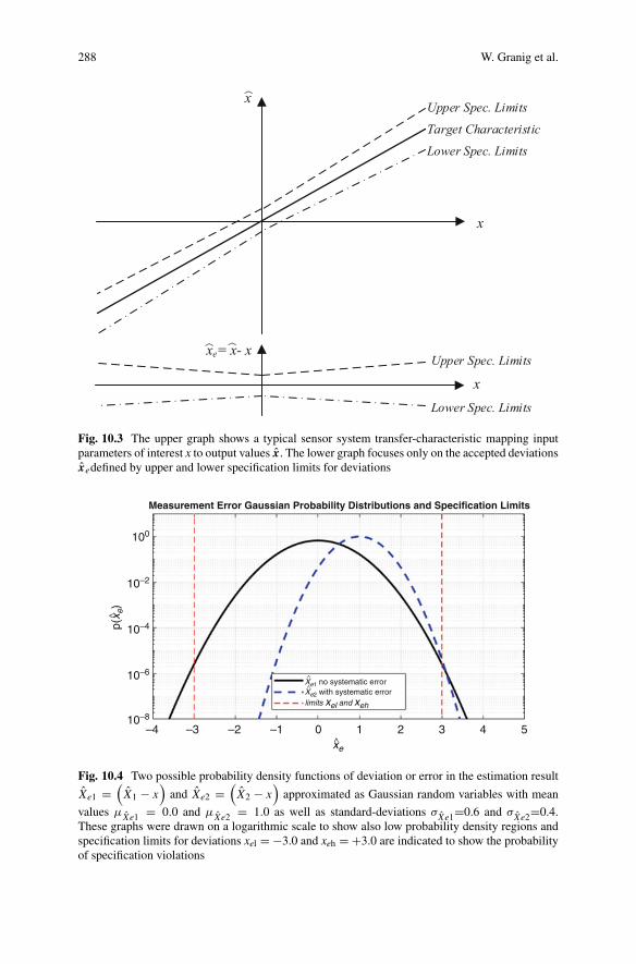
288 W. Granig et al.
x
⟨
Upper Spec. Limits
Lower Spec. Limits
Target Characteristic
⟨
Upper Spec. Limits
Lower Spec. Limits
x
xe= x- x
x
⟨
Fig. 10.3 The upper graph shows a typical sensor system transfer-characteristic mapping inputparameters of interest x to output values x. The lower graph focuses only on the accepted deviationsxedefined by upper and lower specification limits for deviations
100
10–2
10–4p(x e
)
xe
X^e1 no systematic error
X^e2 with systematic error
limits xel and xeh
10–6
10–8
–4 –3 –2 –1
Measurement Error Gaussian Probability Distributions and Specification Limits
0 1 2 3 4 5
Fig. 10.4 Two possible probability density functions of deviation or error in the estimation result
Xe1 =(X1 − x
)and Xe2 =
(X2 − x
)approximated as Gaussian random variables with mean
values μXe1 = 0.0 and μ
Xe2 = 1.0 as well as standard-deviations σXe1=0.6 and σ
Xe2=0.4.These graphs were drawn on a logarithmic scale to show also low probability density regions andspecification limits for deviations xel = −3.0 and xeh = +3.0 are indicated to show the probabilityof specification violations
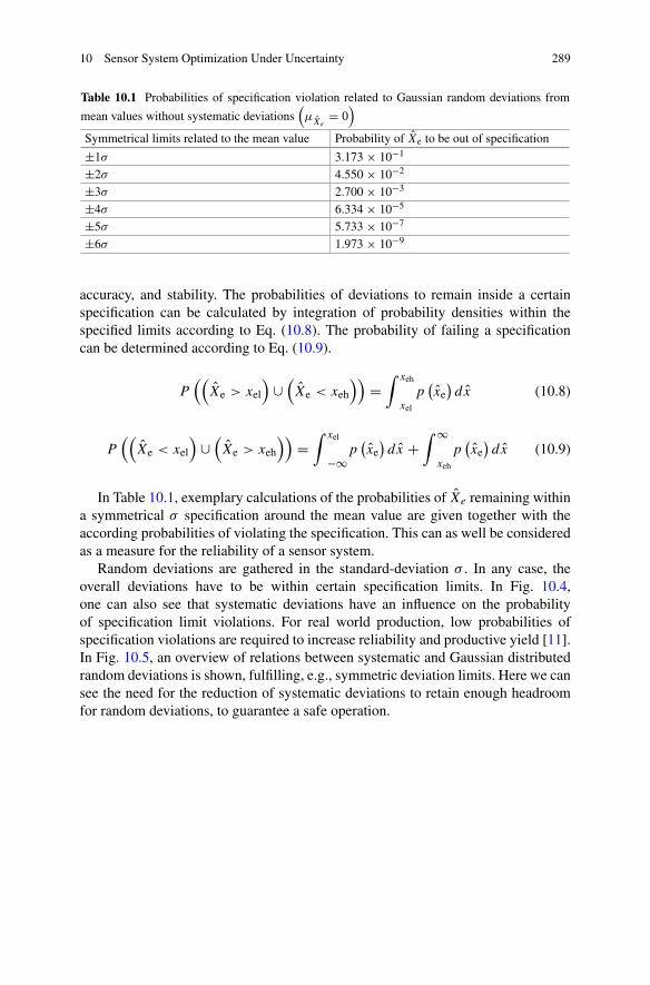
10 Sensor System Optimization Under Uncertainty 289
Table 10.1 Probabilities of specification violation related to Gaussian random deviations from
mean values without systematic deviations(μ
Xe= 0
)
Symmetrical limits related to the mean value Probability of Xe to be out of specification
±1σ 3.173 × 10⁻¹
±2σ 4.550 × 10⁻²
±3σ 2.700 × 10⁻³
±4σ 6.334 × 10⁻⁵
±5σ 5.733 × 10⁻⁷
±6σ 1.973 × 10⁻⁹
accuracy, and stability. The probabilities of deviations to remain inside a certainspecification can be calculated by integration of probability densities within thespecified limits according to Eq. (10.8). The probability of failing a specificationcan be determined according to Eq. (10.9).
P((
Xe > xel
)∪(Xe < xeh
))=∫ xeh
xel
p(xe)dx (10.8)
P((
Xe < xel
)∪(Xe > xeh
))=∫ xel
−∞p(xe)dx +
∫ ∞
xeh
p(xe)dx (10.9)
In Table 10.1, exemplary calculations of the probabilities of Xe remaining withina symmetrical σ specification around the mean value are given together with theaccording probabilities of violating the specification. This can as well be consideredas a measure for the reliability of a sensor system.
Random deviations are gathered in the standard-deviation σ . In any case, theoverall deviations have to be within certain specification limits. In Fig. 10.4,one can also see that systematic deviations have an influence on the probabilityof specification limit violations. For real world production, low probabilities ofspecification violations are required to increase reliability and productive yield [11].In Fig. 10.5, an overview of relations between systematic and Gaussian distributedrandom deviations is shown, fulfilling, e.g., symmetric deviation limits. Here we cansee the need for the reduction of systematic deviations to retain enough headroomfor random deviations, to guarantee a safe operation.
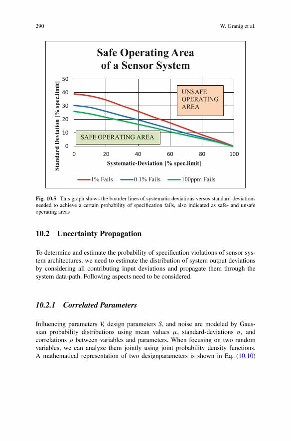
290 W. Granig et al.
0
10
20
30
40
50
0 20 40 60 80 100
Stan
dard
Dev
iatio
n [%
spec
.lim
it]
Systematic-Deviation [% spec.limit]
Safe Operating Areaof a Sensor System
1% Fails 0.1% Fails 100ppm Fails
SAFE OPERATING AREA
UNSAFE OPERATING AREA
Fig. 10.5 This graph shows the boarder lines of systematic deviations versus standard-deviationsneeded to achieve a certain probability of specification fails, also indicated as safe- and unsafeoperating areas
10.2 Uncertainty Propagation
To determine and estimate the probability of specification violations of sensor sys-tem architectures, we need to estimate the distribution of system output deviationsby considering all contributing input deviations and propagate them through thesystem data-path. Following aspects need to be considered.
10.2.1 Correlated Parameters
Influencing parameters V, design parameters S, and noise are modeled by Gaus-sian probability distributions using mean values μ, standard-deviations σ , andcorrelations ρ between variables and parameters. When focusing on two randomvariables, we can analyze them jointly using joint probability density functions.A mathematical representation of two designparameters is shown in Eq. (10.10)
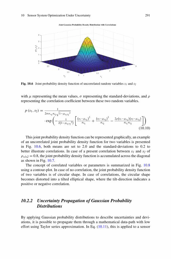
10 Sensor System Optimization Under Uncertainty 291
Fig. 10.6 Joint probability density function of uncorrelated random variables s1 and s2
with μ representing the mean values, σ representing the standard-deviations, and ρ
representing the correlation coefficient between these two random variables.
p (s1, s2) = 1
2πσs1σs2
√1−ρs1s2
2
· exp
(− 1
2(1−ρs1s2
2)[ (
s1−μs1
)2
σs1+
(s2−μs2
)2
σs2− 2ρ
(s1−μs1
)(s2−μs2
)
σs1 σs2
])
(10.10)
This joint probability density function can be represented graphically, an exampleof an uncorrelated joint probability density function for two variables is presentedin Fig. 10.6, both means are set to 2.0 and the standard-deviations to 0.2 tobetter illustrate correlations. In case of a present correlation between s1 and s2 ofρs1s2 = 0.8, the joint probability density function is accumulated across the diagonalas shown in Fig. 10.7.
The concept of correlated variables or parameters is summarized in Fig. 10.8using a contour-plot. In case of no correlation, the joint probability density functionof two variables is of circular shape. In case of correlations, the circular shapebecomes distorted into a tilted elliptical shape, where the tilt-direction indicates apositive or negative correlation.
10.2.2 Uncertainty Propagation of Gaussian ProbabilityDistributions
By applying Gaussian probability distributions to describe uncertainties and devi-ations, it is possible to propagate them through a mathematical data-path with loweffort using Taylor series approximation. In Eq. (10.11), this is applied to a sensor
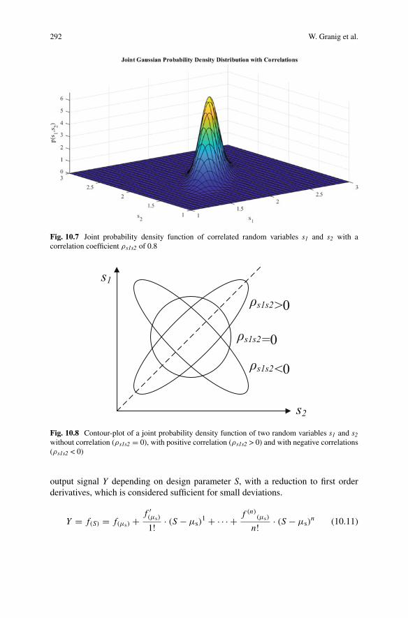
292 W. Granig et al.
Fig. 10.7 Joint probability density function of correlated random variables s1 and s2 with acorrelation coefficient ρs1s2 of 0.8
s1
s2
ρs1s2>0
ρs1s2<0
ρs1s2=0
Fig. 10.8 Contour-plot of a joint probability density function of two random variables s1 and s2without correlation (ρs1s2 = 0), with positive correlation (ρs1s2 > 0) and with negative correlations(ρs1s2 < 0)
output signal Y depending on design parameter S, with a reduction to first orderderivatives, which is considered sufficient for small deviations.
Y = f(S) = f(μs) + f ′(μs)
1! · (S − μs)1 + · · · + f (n)
(μs)
n! · (S − μs)n (10.11)
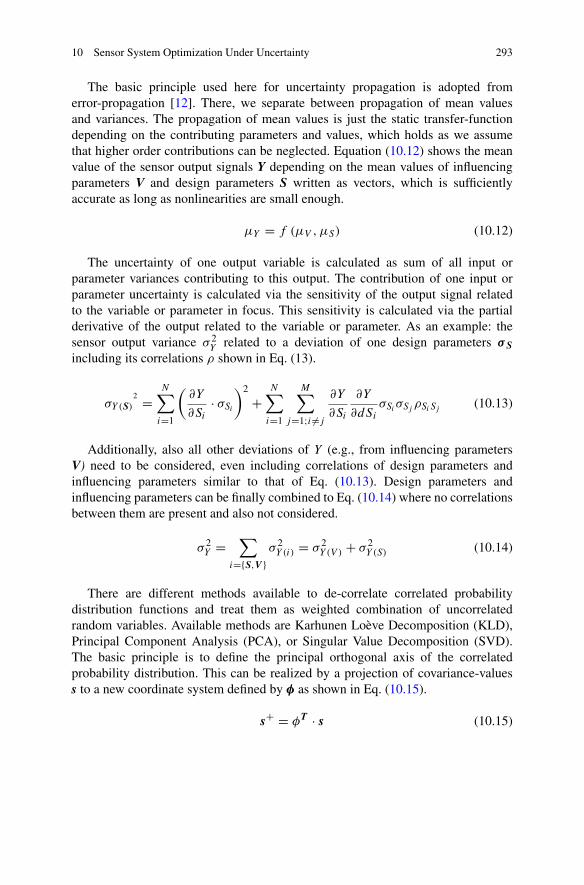
10 Sensor System Optimization Under Uncertainty 293
The basic principle used here for uncertainty propagation is adopted fromerror-propagation [12]. There, we separate between propagation of mean valuesand variances. The propagation of mean values is just the static transfer-functiondepending on the contributing parameters and values, which holds as we assumethat higher order contributions can be neglected. Equation (10.12) shows the meanvalue of the sensor output signals Y depending on the mean values of influencingparameters V and design parameters S written as vectors, which is sufficientlyaccurate as long as nonlinearities are small enough.
μY = f (μV ,μS) (10.12)
The uncertainty of one output variable is calculated as sum of all input orparameter variances contributing to this output. The contribution of one input orparameter uncertainty is calculated via the sensitivity of the output signal relatedto the variable or parameter in focus. This sensitivity is calculated via the partialderivative of the output related to the variable or parameter. As an example: thesensor output variance σ 2
Y related to a deviation of one design parameters σ Sincluding its correlations ρ shown in Eq. (13).
σY(S)2 =
N∑
i=1
(∂Y
∂Si
· σSi
)2
+N∑
i=1
M∑
j=1;i �=j
∂Y
∂Si
∂Y
∂dSi
σSiσSj
ρSiSj(10.13)
Additionally, also all other deviations of Y (e.g., from influencing parametersV) need to be considered, even including correlations of design parameters andinfluencing parameters similar to that of Eq. (10.13). Design parameters andinfluencing parameters can be finally combined to Eq. (10.14) where no correlationsbetween them are present and also not considered.
σ 2Y =
∑
i={S,V }σ 2
Y (i) = σ 2Y (V ) + σ 2
Y (S) (10.14)
There are different methods available to de-correlate correlated probabilitydistribution functions and treat them as weighted combination of uncorrelatedrandom variables. Available methods are Karhunen Loève Decomposition (KLD),Principal Component Analysis (PCA), or Singular Value Decomposition (SVD).The basic principle is to define the principal orthogonal axis of the correlatedprobability distribution. This can be realized by a projection of covariance-valuess to a new coordinate system defined by φ as shown in Eq. (10.15).
s+ = φT · s (10.15)

294 W. Granig et al.
s1=unc(2.0,0.1,‘s1‘)random variable name
random variable standard-uncertainty (σ)random variable mean-value (μ)
random variable definition functionrandom variable
Fig. 10.9 This is an example function defining a random variable for a design parameter s1 usingthe uncertainty toolbox
In our practical example, the new coordinate system φ can be found using theeigenvectors of s. When using this SVD in the data-path, the correlated variablesand parameters are calculated via the transformation matrix, represented by theeigenvectors φ and the uncorrelated values s+ as shown in Eq. (10.16).
d = φ · d+ (10.16)
A software tool for calculating with uncertainties and uncertain variables, espe-cially the propagation of uncertainties through a system data-path was implementedin MATLAB [13]. A first version called “Uncertainty Toolbox” was prepared in aneducational context, including some application examples [14]. The definition of anuncertain variable in MATLAB is shown in Fig. 10.9. This version was improvedby adding features such as the consideration of correlated Gaussian distributions,complex number handling, and decision limits. Also, a function which compares theprobability of one variable to a limit incorporating uncertain numbers was added.A practical application is given for a magneto-resistive angle sensor raw signalanalysis [15]. A summary of implemented functions can be found in Appendix 1.
10.3 Sensor System Optimization Principles
10.3.1 Statistical Optimization Principles
In this section, we elaborate statistical optimization theory using the Fisher infor-mation [16, 17]. In all sensor systems, design- and input-parameter variations arepresent, which must be considered in optimization [18]. Optimization proceduresin general need an optimization criterion. This criterion is defined by ψ and candepend on design parameters S as well as the real input value x. The optimizationof design parameters can be defined as shown in Eq. (17).
s∗ = arg minSε�
� (x,S) (10.17)
10 Sensor System Optimization Under Uncertainty 295
Fig. 10.10 Local and globaloptimum of a designconsidering variations ofdesign parameters. The valueof the optimization criterionachieved for location μs(1) isworse compared to that oflocation μs(2)
The optimization shall not only optimize the sensor system in a certain localoptimum, instead we are interested in a global optimum including design-parametervariations. A graphical representation of this optimization is given in Fig. 10.10.
One commonly used statistical optimization target is the Minimum VarianceUnbiased Estimation (MVUE). Here, the target is to achieve the minimum varianceof an estimator while it has to remain, i.e., hit the true value on average. The amountof information about the variable of interest contained in the measurement data canbe described by the Fisher information I. In the linear case, the inverse of the Fisherinformation I−1 is called dispersion D as defined in Eq. (10.18) and represents alower bound for the variance of an unbiased estimator (see Eq. (10.19)).
D = I−1 (10.18)
var(X)
≥ 1
I (x,S)(10.19)
A general formula for the determination of the Fisher information is givenin Eq. (10.20), which is valid for additive white Gaussian deviations includingconsiderations of their covariance C. Here x represents the real input value and Sthe design parameters.
[I (x,S)]ij [I (x,S)]ij =(
∂h(x,S)∂xi
)T
CY (x,S)−1(
∂h(x,S)∂xj
) (∂h(x,S)
∂si
)T
×CY (x,S)−1(
∂h(x,S)∂sj
)
+ 12 tr
(CY (x,S)−1 ∂CY (x,S)
∂xiCY (x,S)−1 ∂CY (x,S)
∂xj
)
×(C(x,S)−1 ∂C(x,S)
∂siCY (x,S)−1 ∂C(x,S)
∂sj
)
(10.20)

296 W. Granig et al.
In the case of only linear relationships, where the derivative is constant andtherefore independent on the real input value x, and no correlations between theparameters of interest the Fisher information is simplified to Eq. (10.21).
I (S) = h(S)T h(S)
σ 2Y
(10.21)
The Fisher information I, or the inverse known as dispersion D can now be usedto minimize the effect of design-parameter variations. Several characteristics of thedispersion can be used for optimizations [17], one of the most common criteria isbased on a minimization of the determinant of the dispersion, e.g., as in Eq. (10.22).
� (x,S) = minsεS
|D (x,S)| (10.22)
The overall formulation to find the optimum design parameters is given in Eq.(10.23).
s∗ = arg minSε�
maxxεX
|D (x,S)| (10.23)
A practical example of a statistical optimization of design parameters for angularposition sensor systems can be in [19]. The inverse Fisher information representsa lower bound for any unbiased estimator. However, such an estimator may notexist, not be found or not desirable, e.g., due to computational effort. In such cases,when a biased estimator is used, i.e., a systematic deviation (offset) occurs, the meansquare error might be used as optimization criterion [20]. In this chapter we focuson Fisher information optimization only, since systematic deviations are reduced bysensor calibration.
10.3.2 Sensor Calibration
10.3.2.1 Calibration of Sensor System Output
An effective way of improving a sensor performance is to calibrate this sensorsystem using an accurate reference sensor system, or a reference value generator.Typically, sensor systems are calibrated during or at the end of production. This isdone by applying a known physical reference value to the sensor system and com-pensate for the difference between the reference value and the target sensor systemvalue. The dependence of the output and input is often estimated using a linearmodel. To do so, the inverse of the characteristic to be linearized has to be found.The resulting parameters and calibration values are then used to configure the sensorsystem. In this way, we generate compensation parameters which are correlatedto the deviations of the sensor system and therefore can be used to cancel sensor
10 Sensor System Optimization Under Uncertainty 297
system deviations in an effective manner. The necessary calibration measurementsdepend on the defined sensor system architecture calibration algorithms. Importantaspects for the calibration of a sensor system are the respective parameters. Theseparameters have to be defined in advance during the architecture exploration phase,to perform a calibration procedure in the real implementation. Following deviationsbetween reference measurement and sensor system output values can be present:
• Offset Error: If the measurement physical quantity is zero, the sensor systemvalue should also indicate zero. Any deviation in this case is called an offseterror.
• Gain Error/Sensitivity Error: When exiting the physical quantity, a certainpredefined sensitivity is used to indicate it. Any deviation of the linear sensitivity-slope is known as gain error or sensitivity error.
• Nonlinear Errors: Since the gain error can be different at different excitations,a nonlinearity error is present. Typically, these deviations are modeled andcompensated using polynomials. In practical implementations, second or thirdorder polynomials are used.
There are more options available for calibration, such as lookup-tables and piece-wise linear interpolations which need a higher number of calibration points. Anotherway is using polynomial interpolations or segmented polynomial interpolations alsocalled spline interpolations. The most practical way of calibration is a polynomialfitting because of the low number of calibration parameters and calibration points.To find the best fitting calibration parameters, one need to minimize the squarederror of all calibration measurements. This can be done by polynomial regressionalgorithms, which are explained in detail in [21]. First one needs to define the systemwith linear related coefficients as shown in Eq. (10.24) using polynomials and Eq.(10.25) in matrix form.
x =n∑
i=0
yiki (10.24)
x = h · k (10.25)
There h represents the augmented measurement vector, k represents the vector ofcalibration parameters, and x the value of compensated output values. In case of apolynomial calibration of order n, the information matrix is defined as shown in Eq.(10.26) where y represents the sensor output before the estimator or compensation.
h =[y0 · · · yn
](10.26)
Here the first element represents the constant factor used for offset calculations,the second column the unmodified sensor signal, the third column the squared sensorsignals (e.g., for the second order polynomial compensation), etc. The size of the
298 W. Granig et al.
parameter-vector relates to the dimension of information matrix and is shown in Eq.(10.27).
k =⎡
⎢⎣k0...
kn
⎤
⎥⎦ (10.27)
In this parameter-vector k, the first parameter k0 represents the offset value, thesecond parameter k1 the linear gain value, the third parameter k2 the quadraticpolynomial compensation parameter, etc. Finding the best fitting compensationparameters k can be found by least mean square fitting according [16]. Theestimation of calibration parameters is done acc. Eq. (10.28).
k =(H T
calH cal
)−1H T
calxcal (10.28)
Here, k represents the vector of calibration parameters shown in Eq. (10.24),Hcal the augmented observation matrix similar to those shown in Eq. (1026), butincluding rows of all calibration points xcal. Here, xcal represents the vector ofall target output values of the sensor system, measured with a reference systemor defined by known target values. In case of polynomial calibration, the numberof calibration points needs to exceed the polynomial order n by at least one. Theinformation matrix in this case becomes the matrix shown in Eq. (10.29), wherem ≥ n in case m starts to count from 0. For increased performance of estimation,more calibration points are beneficial.
H cal =⎡
⎢⎣y0
cal0 . . . yncal0
.... . .
...
y0calm · · · yn
calm
⎤
⎥⎦ (10.29)
10.3.3 Optimization of Calibration Parameters
Here minimum variance unbiased estimation can be used to find the calibrationpoints generating the lowest variation of the physical parameter of interest. Thiscan also be based on the Fisher information or dispersion. We need to find theparameters which minimize the determinant of the dispersion matrix of the estimatorwith calibration parameters as values of interest (see Eq. (10.30)).
x∗cal = arg min
xεX|D (y, c)| (10.30)
In case of the polynomial error compensation technique, the output is linearlydependent on the values of interest (the calibration parameters), which simplifies

10 Sensor System Optimization Under Uncertainty 299
the optimization acc. Eq. (10.31). The location of the minimum is the same withand without variances because there is no dependency on design parameters presentand therefore it can be neglected.
x∗cal = arg min
xεX
∣∣∣∣(H T H
)−1∣∣∣∣ (10.31)
Interestingly, in case of uncorrelated measurements, the optimization suggests torepeat measurements at the extreme points instead of distributing them uniformlyover the input space. Another interesting aspect is the fact that for this calibrationwe only need the difference between the sensor outputs and the reference value.There is no need for an exact measurement of influencing physical quantities. Onlyan influencing parameter excitation is needed, the internally measured influencingparameter values are used for calibration parameter generation and later onlinecompensation.
10.4 Sensor System Optimization Example
For educational purposes, a simple temperature sensor system application was cho-sen to explain the practical usage of this uncertainty toolbox and to apply statisticalsensor system optimization. Target is to define a sensor system architecture using aPT1000 temperature dependent resistor of accuracy type B to set up a temperaturemeasurement system with an accuracy of +/−3.0 ◦C worst case (+/−3σ standarduncertainty).
10.4.1 Sensor System Modeling Including Uncertainties
A temperature measurement system was chosen which uses a resistive Wheatstone-Bridge for generation of a differential temperature dependent voltage, which isconverted via an analog-digital converter with consecutive digital calibration. Theschematic of this temperature measurement system is shown in Fig. 10.11.
The whole transfer-function of this system can be described as serial connectionof individual transfer-functions of the analog-part including the digital conversionwith mapping to the final physical units, where resistors with indices “0” representthe resistance at 0 ◦C (see Eq. (10.32)).
T = G · V DD ·(
R20 (1 + T C2 · T )
R10 (1 + T C1 · T ) + R20 (1 + T C2 · T )
− R40 (1 + T C4 · T )
R30 (1 + T C3 · T ) + R40 (1 + T C4 · T )
) (10.32)
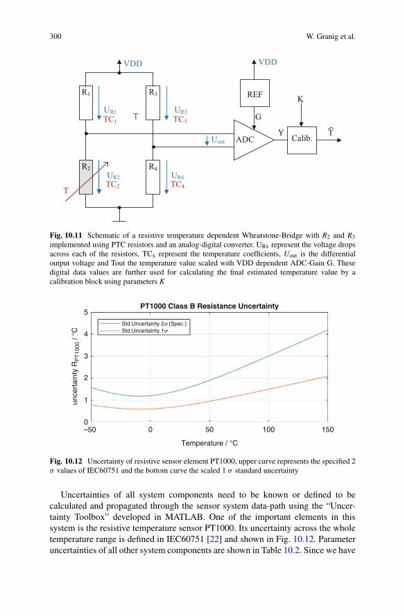
300 W. Granig et al.
UR1 UR3
UR2 UR4
T
T
VDD
TC1 TC3
TC2 TC4
R1
R2
R3
R4
VDD
REF
ADC Calib.
K
TYUout
G
Fig. 10.11 Schematic of a resistive temperature dependent Wheatstone-Bridge with R2 and R3implemented using PTC resistors and an analog-digital converter. URx represent the voltage dropsacross each of the resistors, TCx represent the temperature coefficients, Uout is the differentialoutput voltage and Tout the temperature value scaled with VDD dependent ADC-Gain G. Thesedigital data values are further used for calculating the final estimated temperature value by acalibration block using parameters K
5
4
2
unce
rtai
nty
RP
T10
00 /
°C
3
1
0–50 0
PT1000 Class B Resistance Uncertainty
Std.Uncertainty 2s (Spec.)Std.Uncertainty 1s
50 100 150
Temperature / °C
Fig. 10.12 Uncertainty of resistive sensor element PT1000, upper curve represents the specified 2σ values of IEC60751 and the bottom curve the scaled 1 σ standard uncertainty
Uncertainties of all system components need to be known or defined to becalculated and propagated through the sensor system data-path using the “Uncer-tainty Toolbox” developed in MATLAB. One of the important elements in thissystem is the resistive temperature sensor PT1000. Its uncertainty across the wholetemperature range is defined in IEC60751 [22] and shown in Fig. 10.12. Parameteruncertainties of all other system components are shown in Table 10.2. Since we have
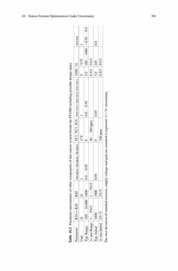
10 Sensor System Optimization Under Uncertainty 301
Tabl
e10
.2Pa
ram
eter
unce
rtai
ntie
sof
othe
rco
mpo
nent
sof
this
sens
orsy
stem
besi
deth
ePT
1000
incl
udin
gpo
ssib
lede
sign
spac
e
Para
met
erR
10=
R30
R40
ρR
10R
30,ρ
R10
R40
,ρR
30R
40T
C1,
TC
3,T
C4
ρT
C1T
C3,ρ
TC
1TC
4,ρ
TC
3TC
4V
DD
Gρ
GV
DD
Uni
t�
�1
1/◦ C
1V
◦ C/V
1Ty
p.R
ange
100
...1
0,00
010
000.
0..
.0.9
50
0.0
...0
.95
5.0
100
...1
000
−0.9
5..
.0.0
1σun
c.R
ange
1..
.5%
/31
...5
%/3
50..
.200
ppm
0.5/
35%
/3Ty
p.In
itial
1000
1000
0.95
00.
955.
024
50.
01σ
unc.
Initi
al2%
/32%
/310
0pp
m0.
5/3
5%/3
The
max
devi
atio
nof
stan
dard
resi
stor
s,su
pply
volta
gean
dga
inar
eas
sum
edto
repr
esen
t+/−
3σun
cert
aint
y
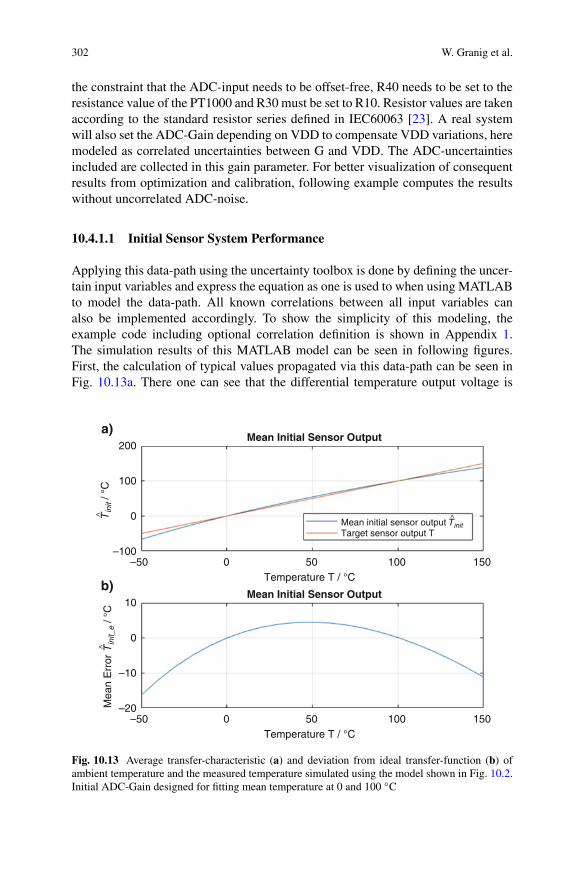
302 W. Granig et al.
the constraint that the ADC-input needs to be offset-free, R40 needs to be set to theresistance value of the PT1000 and R30 must be set to R10. Resistor values are takenaccording to the standard resistor series defined in IEC60063 [23]. A real systemwill also set the ADC-Gain depending on VDD to compensate VDD variations, heremodeled as correlated uncertainties between G and VDD. The ADC-uncertaintiesincluded are collected in this gain parameter. For better visualization of consequentresults from optimization and calibration, following example computes the resultswithout uncorrelated ADC-noise.
10.4.1.1 Initial Sensor System Performance
Applying this data-path using the uncertainty toolbox is done by defining the uncer-tain input variables and express the equation as one is used to when using MATLABto model the data-path. All known correlations between all input variables canalso be implemented accordingly. To show the simplicity of this modeling, theexample code including optional correlation definition is shown in Appendix 1.The simulation results of this MATLAB model can be seen in following figures.First, the calculation of typical values propagated via this data-path can be seen inFig. 10.13a. There one can see that the differential temperature output voltage is
T^ init
/ °C
200
100
0
–100–50 0
Mean Initial Sensor Output
Temperature T / °C
a)
Mean initial sensor output T^init
Target sensor output T
50 100 150
Mea
n E
rror
T^ init_
e / °
C
10
0
–10
–20–50 0
Mean Initial Sensor Output
Temperature T / °C
b)
50 100 150
Fig. 10.13 Average transfer-characteristic (a) and deviation from ideal transfer-function (b) ofambient temperature and the measured temperature simulated using the model shown in Fig. 10.2.Initial ADC-Gain designed for fitting mean temperature at 0 and 100 ◦C
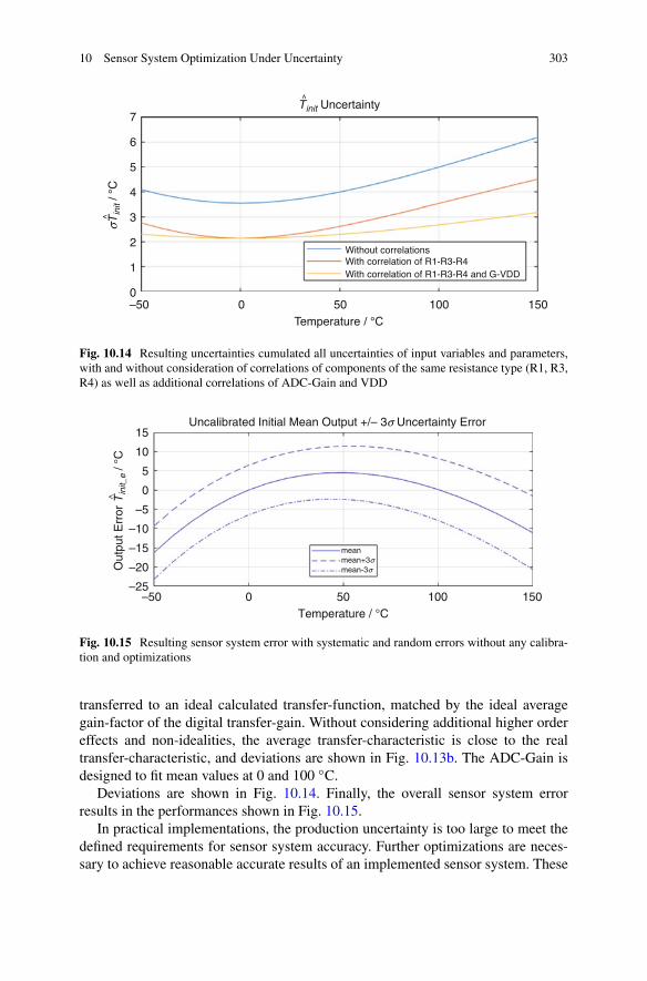
10 Sensor System Optimization Under Uncertainty 303
σT^ in
it / °
CT^init Uncertainty
7
6
5
4
3
1
2
0–50 0
Temperature / °C
Without correlationsWith correlation of R1-R3-R4With correlation of R1-R3-R4 and G-VDD
50 100 150
Fig. 10.14 Resulting uncertainties cumulated all uncertainties of input variables and parameters,with and without consideration of correlations of components of the same resistance type (R1, R3,R4) as well as additional correlations of ADC-Gain and VDD
Out
put E
rror
T^ init_
e / °
C
–20
–15
–10
–5
0
5
10
15
–25–50 0
Temperature / °C
Uncalibrated Initial Mean Output +/– 3s Uncertainty Error
meanmean+3smean-3s
50 100 150
Fig. 10.15 Resulting sensor system error with systematic and random errors without any calibra-tion and optimizations
transferred to an ideal calculated transfer-function, matched by the ideal averagegain-factor of the digital transfer-gain. Without considering additional higher ordereffects and non-idealities, the average transfer-characteristic is close to the realtransfer-characteristic, and deviations are shown in Fig. 10.13b. The ADC-Gain isdesigned to fit mean values at 0 and 100 ◦C.
Deviations are shown in Fig. 10.14. Finally, the overall sensor system errorresults in the performances shown in Fig. 10.15.
In practical implementations, the production uncertainty is too large to meet thedefined requirements for sensor system accuracy. Further optimizations are neces-sary to achieve reasonable accurate results of an implemented sensor system. These
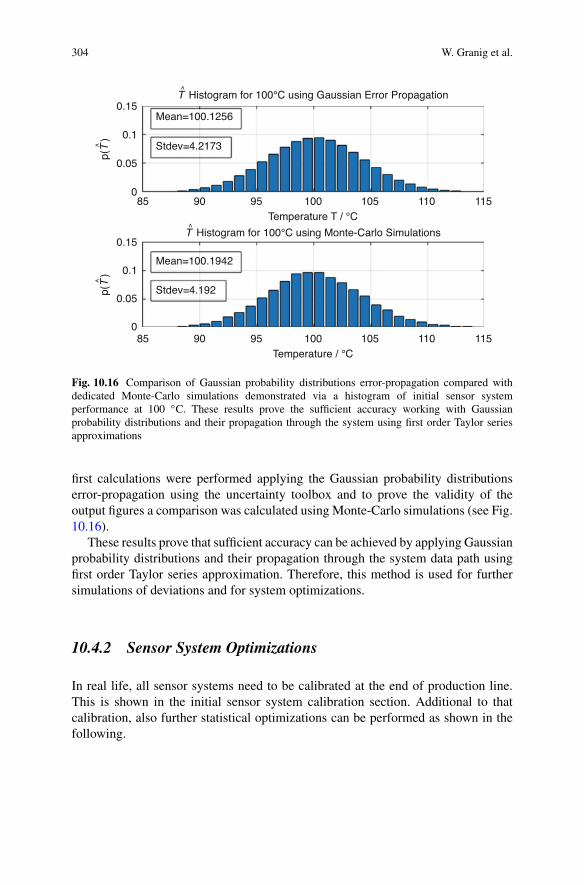
304 W. Granig et al.
p(T^
)0.15
0.1
0.05
085 90 95
Temperature T / °C
Mean=100.1256
Stdev=4.2173
T^ Histogram for 100°C using Gaussian Error Propagation
100 105 110 115
p(T^
)
0.15
0.1
0.05
085 90 95
Temperature / °C
Mean=100.1942
Stdev=4.192
T^ Histogram for 100°C using Monte-Carlo Simulations
100 105 110 115
Fig. 10.16 Comparison of Gaussian probability distributions error-propagation compared withdedicated Monte-Carlo simulations demonstrated via a histogram of initial sensor systemperformance at 100 ◦C. These results prove the sufficient accuracy working with Gaussianprobability distributions and their propagation through the system using first order Taylor seriesapproximations
first calculations were performed applying the Gaussian probability distributionserror-propagation using the uncertainty toolbox and to prove the validity of theoutput figures a comparison was calculated using Monte-Carlo simulations (see Fig.10.16).
These results prove that sufficient accuracy can be achieved by applying Gaussianprobability distributions and their propagation through the system data path usingfirst order Taylor series approximation. Therefore, this method is used for furthersimulations of deviations and for system optimizations.
10.4.2 Sensor System Optimizations
In real life, all sensor systems need to be calibrated at the end of production line.This is shown in the initial sensor system calibration section. Additional to thatcalibration, also further statistical optimizations can be performed as shown in thefollowing.
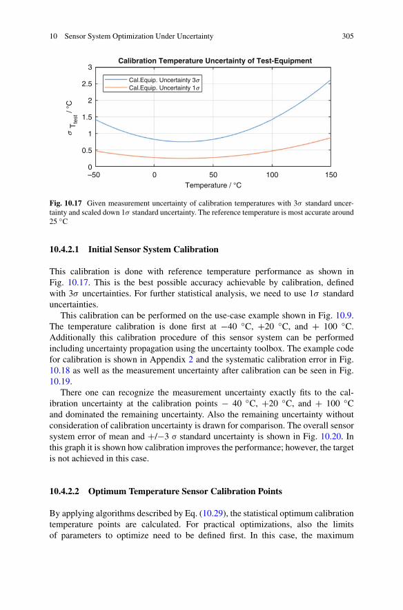
10 Sensor System Optimization Under Uncertainty 305
s T
test
/ °C
0.5
1
1.5
2
2.5
3
0–50 0
Temperature / °C
Calibration Temperature Uncertainty of Test-Equipment
Cal.Equip. Uncertainty 3sCal.Equip. Uncertainty 1s
50 100 150
Fig. 10.17 Given measurement uncertainty of calibration temperatures with 3σ standard uncer-tainty and scaled down 1σ standard uncertainty. The reference temperature is most accurate around25 ◦C
10.4.2.1 Initial Sensor System Calibration
This calibration is done with reference temperature performance as shown inFig. 10.17. This is the best possible accuracy achievable by calibration, definedwith 3σ uncertainties. For further statistical analysis, we need to use 1σ standarduncertainties.
This calibration can be performed on the use-case example shown in Fig. 10.9.The temperature calibration is done first at −40 ◦C, +20 ◦C, and + 100 ◦C.Additionally this calibration procedure of this sensor system can be performedincluding uncertainty propagation using the uncertainty toolbox. The example codefor calibration is shown in Appendix 2 and the systematic calibration error in Fig.10.18 as well as the measurement uncertainty after calibration can be seen in Fig.10.19.
There one can recognize the measurement uncertainty exactly fits to the cal-ibration uncertainty at the calibration points − 40 ◦C, +20 ◦C, and + 100 ◦Cand dominated the remaining uncertainty. Also the remaining uncertainty withoutconsideration of calibration uncertainty is drawn for comparison. The overall sensorsystem error of mean and +/−3 σ standard uncertainty is shown in Fig. 10.20. Inthis graph it is shown how calibration improves the performance; however, the targetis not achieved in this case.
10.4.2.2 Optimum Temperature Sensor Calibration Points
By applying algorithms described by Eq. (10.29), the statistical optimum calibrationtemperature points are calculated. For practical optimizations, also the limitsof parameters to optimize need to be defined first. In this case, the maximum
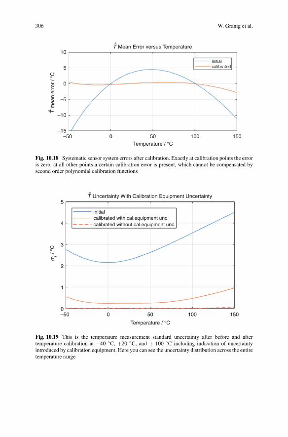
306 W. Granig et al.
–10
–5
0
5
10
–15–50 0
Temperature / °C
T Mean Error versus Temperature
initialcalibrated
50 100 150
T mea
n er
ror
/ °C
Fig. 10.18 Systematic sensor system errors after calibration. Exactly at calibration points the erroris zero, at all other points a certain calibration error is present, which cannot be compensated bysecond order polynomial calibration functions
1
2
3
4
5
0–50 0
Temperature / °C
T Uncertainty With Calibration Equipment Uncertainty
initialcalibrated with cal.equipment unc.calibrated without cal.equipment unc.
50 100 150
σ T^ / °
C
Fig. 10.19 This is the temperature measurement standard uncertainty after before and aftertemperature calibration at −40 ◦C, +20 ◦C, and + 100 ◦C including indication of uncertaintyintroduced by calibration equipment. Here you can see the uncertainty distribution across the entiretemperature range
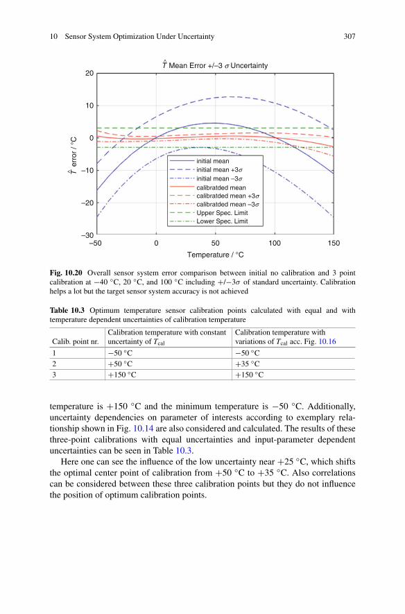
10 Sensor System Optimization Under Uncertainty 307
–20
–10
0
10
20
–30–50 0
Temperature / °C
T Mean Error +/–3 s Uncertainty
initial mean
calibratded mean
initial mean +3s
calibratded mean +3s
initial mean –3s
calibratded mean –3sUpper Spec. LimitLower Spec. Limit
50 100 150
T^ e
rror
/ °C
Fig. 10.20 Overall sensor system error comparison between initial no calibration and 3 pointcalibration at −40 ◦C, 20 ◦C, and 100 ◦C including +/−3σ of standard uncertainty. Calibrationhelps a lot but the target sensor system accuracy is not achieved
Table 10.3 Optimum temperature sensor calibration points calculated with equal and withtemperature dependent uncertainties of calibration temperature
Calib. point nr.Calibration temperature with constantuncertainty of Tcal
Calibration temperature withvariations of Tcal acc. Fig. 10.16
1 −50 ◦C −50 ◦C2 +50 ◦C +35 ◦C3 +150 ◦C +150 ◦C
temperature is +150 ◦C and the minimum temperature is −50 ◦C. Additionally,uncertainty dependencies on parameter of interests according to exemplary rela-tionship shown in Fig. 10.14 are also considered and calculated. The results of thesethree-point calibrations with equal uncertainties and input-parameter dependentuncertainties can be seen in Table 10.3.
Here one can see the influence of the low uncertainty near +25 ◦C, which shiftsthe optimal center point of calibration from +50 ◦C to +35 ◦C. Also correlationscan be considered between these three calibration points but they do not influencethe position of optimum calibration points.

308 W. Granig et al.
10.4.2.3 Optimization of Design Parameters
To optimize design parameters, we can also use the Fisher information and apply themethodology to our temperature measurement system. Since we have no correlation,the Fisher information simplifies to Eq. (10.33).
Iy =(
∂h(x,s)∂s
)2
σ 2y
(10.33)
Since we only have one output y of the sensor frontend, we only need tomaximize the square of derivative of h(·) related to the output variance. In caseof systematic deviations significantly lower than the uncertainties, the Fisherinformation can be used for optimizations. The optimization results in the selectionof design parameters shown in Table 10.4.
The Fisher-optimization result shows that the selection of the resistance valuesof R10 and R30 shall be of the same size as the PT1000 at 0◦C. The temperature-coefficient standard-deviation of R3 has to be 90 ppm to match with the PT1000,others remain at lowest possible value. The resistance uncertainties need to besmallest possible. The correlation of R10 and R40 as well as the temperaturecoefficient correlation shall be 0.0, the other resistance correlations shall be largestpossible. For best results also, the largest negative correlation between G andVDD need to be chosen to compensate VDD-variation effects. The optimizationresults can be also seen in the uncertainties of calibration parameters. A comparisonbetween initial calibration and optimized parameter uncertainties can be seen inTable 10.5.
10.5 Results Including Sensor System Optimizationsof Design Parameters and Calibration-PointOptimization
The results of the optimized system can be seen in the following figures where thesystematic errors and uncertainty dependent on the measurement temperature aredrawn in comparison to the initial defined system. Figure 10.21 shows the system-atic deviations initially, after first calibration and after sensor system optimization.There can be seen that after optimization the remaining mean error is distributedmore symmetrically between positive and negative deviations.
In Fig. 10.22 one can see the measurement uncertainties of the initial system,the system after calibration and after the system optimization. There in Fig.10.22a the uncertainty without consideration of calibration equipment uncertaintiesis shown including the positive effect of calibration-point optimization. In Fig.10.22b, the uncertainty with calibration equipment is drawn including presentation
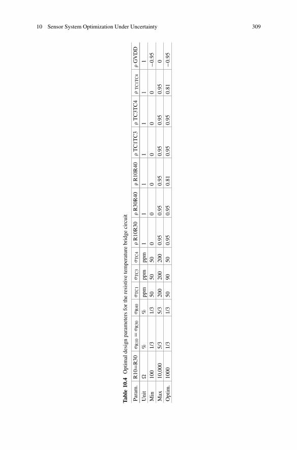
10 Sensor System Optimization Under Uncertainty 309
Tabl
e10
.4O
ptim
alde
sign
para
met
ers
for
the
resi
stiv
ete
mpe
ratu
rebr
idge
circ
uit
Para
m.
R10
=R30
σR
10=
σR
30σ
R40
σT
C1
σT
C3
σT
C4
ρR
10R
30ρ
R30
R40
ρR
10R
40ρ
TC
1TC
3ρ
TC
3TC
4ρ
TC
1TC
4ρ
GV
DD
Uni
t�
%%
ppm
ppm
ppm
11
11
11
1M
in10
01/
31/
350
5050
00
00
00
−0.9
5M
ax10
,000
5/3
5/3
200
200
200
0.95
0.95
0.95
0.95
0.95
0.95
0O
ptim
.10
001/
31/
350
9050
0.95
0.95
0.81
0.95
0.95
0.81
−0.9
5
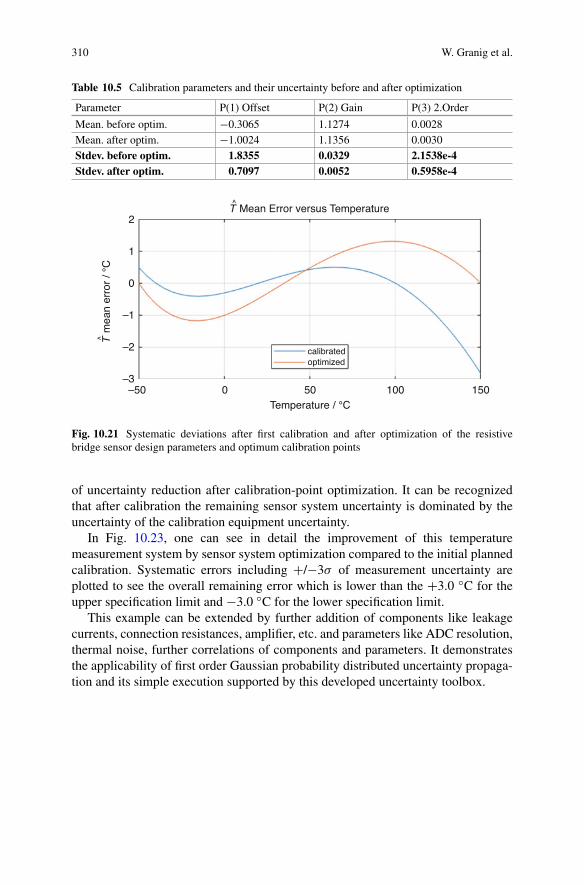
310 W. Granig et al.
Table 10.5 Calibration parameters and their uncertainty before and after optimization
Parameter P(1) Offset P(2) Gain P(3) 2.Order
Mean. before optim. −0.3065 1.1274 0.0028Mean. after optim. −1.0024 1.1356 0.0030Stdev. before optim. 1.8355 0.0329 2.1538e-4Stdev. after optim. 0.7097 0.0052 0.5958e-4
–2
–1
0
1
2
–3–50 0
Temperature / °C
T Mean Error versus Temperature
calibratedoptimized
50 100 150
T mea
n er
ror
/ °C
Fig. 10.21 Systematic deviations after first calibration and after optimization of the resistivebridge sensor design parameters and optimum calibration points
of uncertainty reduction after calibration-point optimization. It can be recognizedthat after calibration the remaining sensor system uncertainty is dominated by theuncertainty of the calibration equipment uncertainty.
In Fig. 10.23, one can see in detail the improvement of this temperaturemeasurement system by sensor system optimization compared to the initial plannedcalibration. Systematic errors including +/−3σ of measurement uncertainty areplotted to see the overall remaining error which is lower than the +3.0 ◦C for theupper specification limit and −3.0 ◦C for the lower specification limit.
This example can be extended by further addition of components like leakagecurrents, connection resistances, amplifier, etc. and parameters like ADC resolution,thermal noise, further correlations of components and parameters. It demonstratesthe applicability of first order Gaussian probability distributed uncertainty propaga-tion and its simple execution supported by this developed uncertainty toolbox.
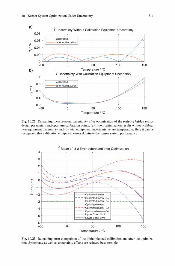
10 Sensor System Optimization Under Uncertainty 311
0.02
0.04
0.06
0.08
a)
0–50 0
calibratedafter optimization
Temperature / °C
T Uncertainty Without Calibration Equipment Uncertainty
50 100 150
σ T^ / °
C
0.4
0.6
0.8
1
b)
0.2–50 0
calibratedafter optimization
Temperature / °C
T Uncertainty With Calibration Equipment Uncertainty
50 100 150
σ T^ / °
C
Fig. 10.22 Remaining measurement uncertainty after optimization of the resistive bridge sensordesign parameters and optimum calibration points. (a) shows optimization results without calibra-tion equipment uncertainty and (b) with equipment uncertainty versus temperature. Here it can berecognized that calibration equipment errors dominate the sensor system performance
–4
–5
–3
–2
–1
0
1
2
4
3
–6–50 0
Temperature / °C
T Mean +/–3 s Error before and after Optimization
Calibrated meanCalibrated mean +3s
Optimized mean +3s
Calibrated mean –3s
Optimized mean –3sUpper Spec. LimitLower Spec. Limit
Optimized mean
50 100 150
T Err
or /
°C
Fig. 10.23 Remaining error comparison of the initial planned calibration and after the optimiza-tion. Systematic as well as uncertainty effects are reduced best possible

312 W. Granig et al.
10.6 Summary
In this chapter, we showed how sensor system architectures can be treated andoptimized in a very early stage of sensor system development based on Gaussianprobability distribution models for component deviations. This simplification toGaussian probability distributions is a reasonable approximation because of itsnatural presence and the argumentation based on the central limit theorem. Thisalso enables an easy handling in propagations through sensor system data-paths.Software tools nowadays are available to perform these statistical uncertaintypropagations and a tool using MATLAB has been developed which enables theseuncertainty propagations even including correlations of parameter deviations. Sucha tool environment can be used for statistical system optimizations too. Statis-tical optimizations of uncertainties using the Fisher information were presentedas well as the optimizations of calibration parameters and optimum calibrationpoints. A practical example based on a resistive PT1000 temperature measurementbridge including calibration considerations and sensor system optimization wasshown including the presentation of how this statistical optimization improvesthe remaining measurement uncertainty to achieve certain sensor system accuracy.This performance-target could be achieved in an easy manner using this statisticaloptimization procedure and according tooling.
Appendix 1: Uncertainty Toolbox in MATLAB, ImplementedFunctions
• Definition of random variables by mean value, standard-deviation, and name
– Set/Get Mean value– Set/Get Standard-Deviation value– Set/Get Name
• Basic mathematical operations implemented by operator overloading
– Addition (Parametric, Matrix)– Subtraction (Parametric, Matrix)– Multiplication (Parametric, Matrix, Element-Wise)– Division (Parametric, Matrix, Element-Wise)– Power (Parametric, Matrix)– Inversion (Matrix)– Determinant (Matrix)– Trigonometric Functions (Matrix)– Hyperbolic Functions (Matrix)
• Special Operations on Arrays
– Determinant– Inverse Matrix
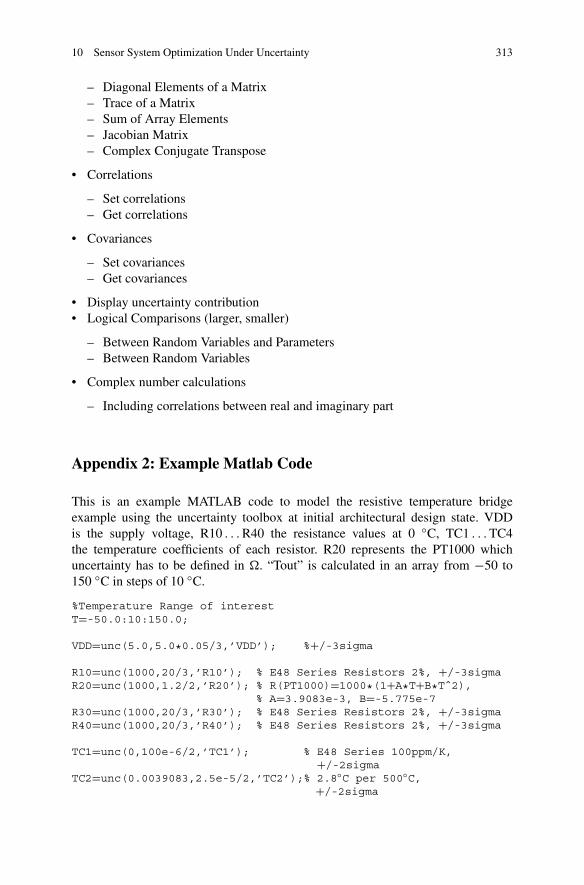
10 Sensor System Optimization Under Uncertainty 313
– Diagonal Elements of a Matrix– Trace of a Matrix– Sum of Array Elements– Jacobian Matrix– Complex Conjugate Transpose
• Correlations
– Set correlations– Get correlations
• Covariances
– Set covariances– Get covariances
• Display uncertainty contribution• Logical Comparisons (larger, smaller)
– Between Random Variables and Parameters– Between Random Variables
• Complex number calculations
– Including correlations between real and imaginary part
Appendix 2: Example Matlab Code
This is an example MATLAB code to model the resistive temperature bridgeexample using the uncertainty toolbox at initial architectural design state. VDDis the supply voltage, R10 . . . R40 the resistance values at 0 ◦C, TC1 . . . TC4the temperature coefficients of each resistor. R20 represents the PT1000 whichuncertainty has to be defined in �. “Tout” is calculated in an array from −50 to150 ◦C in steps of 10 ◦C.
%Temperature Range of interestT=-50.0:10:150.0;
VDD=unc(5.0,5.0*0.05/3,’VDD’); %+/-3sigma
R10=unc(1000,20/3,’R10’); % E48 Series Resistors 2%, +/-3sigmaR20=unc(1000,1.2/2,’R20’); % R(PT1000)=1000*(1+A*T+B*Tˆ2),
% A=3.9083e-3, B=-5.775e-7R30=unc(1000,20/3,’R30’); % E48 Series Resistors 2%, +/-3sigmaR40=unc(1000,20/3,’R40’); % E48 Series Resistors 2%, +/-3sigma
TC1=unc(0,100e-6/2,’TC1’); % E48 Series 100ppm/K,+/-2sigma
TC2=unc(0.0039083,2.5e-5/2,’TC2’);% 2.8◦C per 500◦C,+/-2sigma

314 W. Granig et al.
TC3=unc(0,100e-6/2,’TC3’); % E48 Series 100ppm/K, +/-2sigmaTC4=unc(0,100e-6/2,’TC4’); % E48 Series 100ppm/K, +/-2sigma
G=unc(245,245*0.05/3,’G’); %K/V, defined by Bandgap 5%, +/-3sigma
% with optional correlations R1-R3-R4set_correl (R10,R30,0.95);set_correl (R30,R40,0.95);set_correl (R10,R40,0.95);set_correl (TC1,TC3,0.95);set_correl (TC3,TC4,0.95);set_correl (TC1,TC4,0.95);set_correl (G,VDD,0.0);
R1=R10*(1+TC1*T);R2=R20*(1+TC2*T);R3=R30*(1+TC3*T);R4=R40*(1+TC4*T);
U12R=R2./(R1+R2);U34R=R4./(R3+R4);Uout=VDD*(U12R-U34R);T_hat=Uout*G;
Appendix 3: Matlab Calibration Code
This is an example MATLAB code to model the calibration of the resistivetemperature bridge example using the uncertainty toolbox. The calibration temper-atures “Tx_calunc” are defined with −40 ◦C, +20 ◦C, and + 100 ◦C with givenuncertainties.
%calibration temperatures with uncertaintiesT1_calunc=unc(-40,0.25+((-40-25)ˆ2)/25000,’T1_calunc’);T2_calunc=unc(20,0.25+((20-25)ˆ2)/25000,’T2_calunc’);T3_calunc=unc(100,0.25+((100-25)ˆ2)/25000,’T3_calunc’);
%calibration parametersH_cal=[1 T_hat(2) T_hat(2)ˆ2;... %-40◦C
1 T_hat(8) T_hat(8)ˆ2;... %20◦C1 T_hat(16) T_hat(16)ˆ2]; %100◦C
T_cal=[T1_calunc; T2_calunc; T3_calunc];K_cal=inv(H_cal’*H_cal)*H_cal’*T_cal;
%calibration calculationfor n=1:length(T)T_hat_cal(n)=([1 T_hat(n) T_hat(n)ˆ2]*K_cal);
end
10 Sensor System Optimization Under Uncertainty 315
Glossary
x, x Measurement system real input value, input vectory, y, Y,Y Measurement system indication value, value-vector, RV, RV-vectorx, x, X, X Measurement system estimated value, estimated vector, RV, RV-
vector
v, v, V ,V Influencing parameter, parameter-vector, RV, RV-vectors, s, S,S Design parameter, parameter-vector, RV, RV-vectork, k,K,K Calibration parameter, parameter-vector, RV, RV-vectorw,w,W,W Random zero mean deviations, deviation vector, RV, RV-vector
h Augmented measurement vectorH Augmented observation matrix
I Fisher InformationD DispersionC Covariance Matrix
References
1. N. Beringer, Sensor-based learning—one step closer to autonomous driving, Springer Book,Fahrerassistenzsysteme 2017, May 2017
2. N. Druml, G. Fleischmann, C. Heidenreich, A. Leitner, T. Herndl, G. Hohlweg, Time-of-flight 3D imaging for mixed-critical systems, in Proceedings of the IEEE 13th InternationalConference on Industrial Informatics (INDIN), (2015), pp. 1432–1437
3. L. Wang, A. Cavallaro, Acoustic sensing from a multi-rotor drone. IEEE Sensors J. 18(11),413–427 (2018)
4. M. Rossi, D. Brunelli, Autonomous gas detection and mapping with unmanned aerial vehicles.IEEE Transaction on Instrumentation and Measurement 65(4), 765–775 (2016)
5. P.-Y. Kuo, G. Huang, D. Zhou, An efficient method for evaluating analog circuit performancebounds under process variations. IEEE Transactions on Circuits and Systems 59(6), 351–355(2012)
6. M. Kampl, H. Kosina, The backward Monte Carlo method for semiconductor device simula-tion. J. Comput. Electron. (2018)
7. A. Canelas, R. Martins, R. Povoa, N. Louenco, N. Horta, Yield optimization using K-means clustering algorithm to reduce Monte Carlo simulations, in Design Automation & TestConference and Exhibition (DATE), (2017), pp. 1201–1206
8. JCGM 100:2008, Evaluation of Measurements—Guide to the Expression of Uncertainty inMeasurements (2008)
9. JCGM 200:2012, International Vocabulary of Metrology—Basical and General Concepts andAssociated Terms (VIM) (2012)
10. H.P. Hsu, Theory and Problems of Probability, Random Variables, and Random Process(McGrawHill, New York, 1997)
11. W. Granig, L.M. Faller, H. Zangl, Sensor system optimization to meet reliability targets.Microelectron. Reliab. 87, 113–124 (2018)
12. K.O. Arras, “An Introduction to Error Propagation: Deviation, Meaning and Example ofEquation Cy=FxCxFxT”, Technical Report EPFL-AST-TR-98-01 R3 (EPFL, Lausanne, 1998)

316 W. Granig et al.
13. Mathworks GmbH, MATLAB, version R2017b, September 14 (2017)14. H. Zangl, K. Hoermaier, Educational aspects of uncertainty calculation with software tools.
Measurement 101, 257–264 (2017)15. W. Granig, S. Aoudjit, L.M. Faller, H. Zangl, Statistical modeling of integrated sensors for
automotive applications, in Conference Proceedings, Automotive 2018, Milano, (2018)16. S. Kay, in Fundamentals of Statistical Signal Processing: Estimation Theory, Prentice Hall
Signal Processing Series, ed. by A. V. Oppenheim, (Prentice Hall, Englewood Cliffs, NJ, 1993)17. V. Fedorov, P. Hackl, Model oriented Design of Experiments, (Springer, 1997)18. H. Zangl, G. Steiner, Optimal design of multi-parameter multi-sensor systems. IEEE Trans.
Instrum. Meas. 57, 1484–1491 (2008)19. H. Zangl, L.M. Faller, W. Granig, Optimal design of angular position sensors. COMPEL 36(5),
1372–1385 (2017)20. L.M. Faller, H. Zangl, Robust design of a 3D- and inkjet-printed capacitive force/pressure
sensor. IEEE Proc. EuroSimE (2016)21. J. Fox, Applied Regression Analysis & Generalized Linear Models, 3rd edn. (Sage, Thousand
Oaks, CA, 2016)22. International Electrotechnical Commission, IEC 60751: 2008 Industrial Platinum Resistance
Thermometers and Platinum Temperature Sensors, 2nd edn. (2008)23. International Electrotechnical Commission, IEC 60063: 2015 Preferred Number Series for
Resistors and Capacitors, Edition 3.0 (2015)

Chapter 11Reliability of IoT Sensor Systems:New Methods for the Efficientand Comprehensive ReliabilityAssessment
J. Albrecht, G. Gadhiya, and S. Rzepka
Abbreviations
DA Die attachDA_CTE1 Coefficient of thermal expansion of the die attach materialDA_EX Young’s modulus of the die attach materialDIL Dual in-line packageDMA Dynamic mechanical analysisDoE Design of experimentFOWLP Fan-out wafer-level packageIoT Internet of thingsLF LeadframeMC_CTE1 Coefficient of thermal expansion of the encapsulation (mold
compound) materialMC_EX Young’s modulus of the encapsulation (mold compound) mate-
rialMC_TG Glass transition temperature of the encapsulation (mold com-
pound) materialobj_ST_DP_MC Interface stresses at the interface between mold-die pad as an
objective for the optimizationPCB Printed circuit boardPoP Package on packageRDL Redistribution layerSiP System-in-packageST_DP_DA Interface stresses at the interface between die pad-die attach
J. Albrecht (�) · G. Gadhiya · S. RzepkaMicro Materials Center at Fraunhofer ENAS, Chemnitz, Germanye-mail: [email protected]
© Springer Nature Switzerland AG 2020W. D. van Driel et al. (eds.), Sensor Systems Simulations,https://doi.org/10.1007/978-3-030-16577-2_11
317
318 J. Albrecht et al.
ST_LEAD Interface stresses at the interface between mold-lead pinsST_DP_MC Interface stresses at the interface between mold-die padTMA Thermo-mechanical analysisZ_DA Thickness of die attach
11.1 Introduction
The internet of things (IoT) with its many applications in the fields of automotive,industrial, and personal electronics require innovative electronic systems offeringvarious new functionalities within shortest time-to-market yet with high relia-bility, functional safety, and at costs low enough to be acceptable for the massmarket. Highly integrated circuits as well as packaging solutions are necessaryto fulfill those demands. System-in-package (SiP) based on fan-out wafer-levelpackage (FOWLP) [1], package on package (PoP), or interposer solutions as wellas 3D technologies (die stacks, wafer stacks, package stacks) are able to meetthese technical requirements and performance expectations. Typically, those newminiaturized and highly integrated systems comprise different active and passivecomponents made of different materials, which all have their specific and verydiverse properties regarding thermal expansion and stiffness. Hence, they behavevery differently under thermal and mechanical loading conditions resulting inthermo-mechanical stresses inside the package, which finally may lead to fatigueand failures. These conditions occur during fabrication as well as during the servicelife so that they need to be captured by the qualification tests. Therefore, thethermo-mechanical risks shall be assessed during the development of the packagein order to select the right materials and choose the most suited process steps formaximum production yield but also to fulfill the reliability demands. Unfortunately,comprehensive thermo-mechanical assessments and reliability tests are very costlyand time consuming. Here, virtual prototyping based on numerical models offers anattractive alternative [2, 3].
The utilization of virtual techniques like finite element (FE) simulation canprovide deep insights into the thermo-mechanical stress state of those systemsduring fabrication and service life. Furthermore, they can be used for lifetimeprediction. By this, it is possible to reduce the time for design and testing. Whilesimulations are done within few hours, the physical tests would take several months.However, the most important prerequisite is to have accurate input parameters,which means geometry parameters, well-suited material models with all the requiredmaterial data as well as the consideration of all relevant process steps and service ortest conditions, respectively. The collection of the input parameters is frequently acomplicated, long and costly process. However, once these parameters are available,virtual prototyping becomes a very efficient method not just for the specific designbut for many other similar developments as well. Of course, the models need to bevalidated before being used for the assessment of new products. This is done bycomparing the simulation results to those of experimental tests in order to ensurethe correctness of the predictions based on the simulations.
11 Reliability of IoT Sensor Systems: New Methods for the Efficient. . . 319
This chapter describes the methodology of acquiring the input data and ofperforming the validation for the virtual prototyping of DIL packages as aninstructive example.
11.2 Models for Virtual Prototyping of IoT Sensor Systems
For virtual prototyping based on numerical models, fully parametric FE models arean essential requirement. There are different ways to define parametric FE models.Mostly, parametrization includes the variation of material properties or geometricaldimensions of a component as a parameter, e.g., the thickness of the layer ofmaterials. It does not change the basic geometry such as the number of keypoints,lines, areas, or volumes. Therefore, the FE mesh can be the same during thesevariations. A more complex way would also include changes in the basic geometryof the components or changes in the number of components within same model. Thisleads to a change in the number of keypoints, lines, areas, volumes and requiresa different meshing. So far, most of the attempts to create parametric FE modelsfollow the first way [3–5] while less work has been reported for also including basicgeometry variations or topological changes. One example shall briefly be outlinedhere. The parametric FE modeling is capable of covering wide variations in SiPproducts based on the FOWLP technology. It is based upon a clear hierarchicalarchitecture approach defining groups of similar SiP structures (Fig. 11.1) dividedinto several levels of building blocks, for which a library of parametric modelshas been established using ANSYS™ [7] and comprehensively pre-calibrated. Alllevel of packaging components: multiple dies, molding compound, redistributionlayers (RDLs), solder balls, vias, passives, and PCB board are integrated in thiscomprehensive set of models.
Fig. 11.1 Groups ofsimilarly complex SiPcomponents ([6], withpermission)
320 J. Albrecht et al.
Fig. 11.2 Flowchart forparametric FE modeling for asystem of models ([8], withpermission)
The ANSYS APDL macros (Ansys parametric design language) for creatingthe FE models have been represented in flowchart form in Fig. 11.2. The processstarts by defining the geometry parameters, material definitions, element definitions,and real constants followed by five main modeling steps. The first step createsparametric areas, performs the complex areas subtraction retaining the given areanumbers, creates areas mesh, extrudes areas to create volumetric mesh and assignsmaterial properties to volume elements. This step gives the flexibility to createcomplex geometries and FE models for any combination of components likemultiple dies, vias, and passive devices. The next step creates FE part models ofdifferent types of solder balls, vias, and passives by calling different sub-macrofiles. After that, the solder ball matrix is created by copying the part models fromprevious step. In the fourth step, the remaining package region outside the solder ballmatrix is modeled with or without the underfill. Finally, the Multi-Point Constraint(MPC) based contact elements are created between the FE models which have meshdissimilarity.
After completing the model for a single layer of electronic packages, the routinecan repeat all the steps again in order to create the second layer for the PoPconfiguration. This option is selected by defining the switch parameter PoP = 1.If PoP = 0 the boundary conditions are applied and finally, the FE analysis isperformed according to the load steps and the results are extracted. The part modelscreated within the modeling process can be assembled very flexibly—controlled byanother dedicated parametric script. In this way, the system of fully parametric FEmodels is very well capable of replicating many different SiP products covering allthree groups as shown in Fig. 11.1.
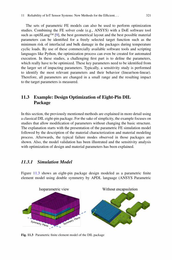
11 Reliability of IoT Sensor Systems: New Methods for the Efficient. . . 321
The sets of parametric FE models can also be used to perform optimizationstudies. Combining the FE solver code (e.g., ANSYS) with a DoE software toolsuch as optiSLang™ [9], the best geometrical layout and the best possible materialparameters can be identified for a freely selected target function such as theminimum risk of interfacial and bulk damage in the packages during temperaturecyclic loads. By use of these commercially available software tools and scriptinglanguages like Python, the optimization process can even be created for automatedexecution. In these studies, a challenging first part is to define the parameters,which really have to be optimized. These key parameters need to be identified fromthe larger set of impacting parameters. Typically, a sensitivity study is performedto identify the most relevant parameters and their behavior (linear/non-linear).Therefore, all parameters are changed in a small range and the resulting impactto the target parameters is measured.
11.3 Example: Design Optimization of Eight-Pin DILPackage
In this section, the previously mentioned methods are explained in more detail usinga classical DIL eight-pin package. For the sake of simplicity, the example focuses onstudies that allow modification of parameters without changing the basic structure.The explanation starts with the presentation of the parametric FE simulation modelfollowed by the description of the material characterization and material modelingprocess. Afterwards, the typical failure modes observed in those packages areshown. Also, the model validation has been illustrated and the sensitivity analysiswith optimization of design and material parameters has been explained.
11.3.1 Simulation Model
Figure 11.3 shows an eight-pin package design modeled as a parametric finiteelement model using double symmetry by APDL language (ANSYS Parametric
Fig. 11.3 Parametric finite element model of the DIL package
322 J. Albrecht et al.
Design Language) within the commercial FE software ANSYS. The base of themodel is the silicon die in the middle of the package. It is attached on the leadframe(copper) by a die attach. The housing of the chip is an encapsulation material madeof an epoxy filled with silica particles. The electrical contacts between the chip andthe lead pads are realized by bond wires, which do not have to be considered inthe model as they have no significant mechanical effect. The FE model consistsof nearly 55,000 nodes and elements. For the validation of the model, the initialinput parameters like material properties still may need to be changed depending onexperimental measurements.
11.3.2 Material Characterization
Table 11.1 summarizes the typical materials used for DIL packages and the consid-ered thermo-mechanical behavior. Intensive investigations in the field of polymers(adhesives, encapsulation) have shown that the properties of these materials arestrongly time and temperature dependent. They show relaxation (decreasing stressunder constant deformation state) and creep behavior (increasing deformation underconstant mechanical loading). A linear visco-elastic material model can describethis time and temperature dependency. The material characterization can be done bydynamic mechanical analysis (DMA), where a frequency sweep is used to extractthe elastic response of a material under variation of the loading frequency andtemperature. This results in a characteristic curve as shown in Fig. 11.4. Furthermaterials of a classical DIL package are silicon, which is modeled as linear elasticstructure, and copper with elastic-plastic behavior. The mechanical behavior of thesematerials is dependent upon the field of application (thermal exposure).
Materials used in a DIP package are typically copper (leadframe), silicon(chip), the encapsulation material (mold compound), and the die attach (polymericadhesives), see summary in Table 11.1. The objects of the optimization routine forthe DIL package are the interfaces between the materials. Therefore, critical valuesfor the interface toughness are necessary. Table 11.3 summarizes the interfacesconsidered here and an assortment of typical test methods to determine the interfacetoughness parameters.
Table 11.1 Mechanical behavior of materials for electronic packages (under typical loadingcondition—thermal cycle between −50 ◦C and +150 ◦C)
Material Example Mechanical behavior
Silicon (with active and passivelayers)
Die Linear elastic
Solder Solder balls Elastic, elastic plastic, creep, cyclicbehavior
Metals Leadframe Elastic, elastic plasticAdhesives Die attach Visco-elastic, visco-plasticFilled polymers Encapsulation Visco-elastic
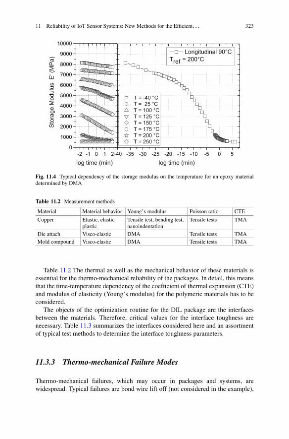
11 Reliability of IoT Sensor Systems: New Methods for the Efficient. . . 323
-40 -35 -30 -25 -20 -15 -10 -5 0 5
T = -40 °C T = 25 °C T = 100 °C T = 125 °C T = 150 °C T = 175 °C T = 200 °C T = 250 °C
-2 -1 0 1 20
1000
2000
3000
4000
5000
6000
7000
8000
9000
10000St
orag
e M
odul
us E
' (M
Pa)
log time (min)
Longitudinal 90°CTref = 200°C
log time (min)
Fig. 11.4 Typical dependency of the storage modulus on the temperature for an epoxy materialdetermined by DMA
Table 11.2 Measurement methods
Material Material behavior Young’s modulus Poisson ratio CTE
Copper Elastic, elasticplastic
Tensile test, bending test,nanoindentation
Tensile tests TMA
Die attach Visco-elastic DMA Tensile tests TMAMold compound Visco-elastic DMA Tensile tests TMA
Table 11.2 The thermal as well as the mechanical behavior of these materials isessential for the thermo-mechanical reliability of the packages. In detail, this meansthat the time-temperature dependency of the coefficient of thermal expansion (CTE)and modulus of elasticity (Young’s modulus) for the polymeric materials has to beconsidered.
The objects of the optimization routine for the DIL package are the interfacesbetween the materials. Therefore, critical values for the interface toughness arenecessary. Table 11.3 summarizes the interfaces considered here and an assortmentof typical test methods to determine the interface toughness parameters.
11.3.3 Thermo-mechanical Failure Modes
Thermo-mechanical failures, which may occur in packages and systems, arewidespread. Typical failures are bond wire lift off (not considered in the example),
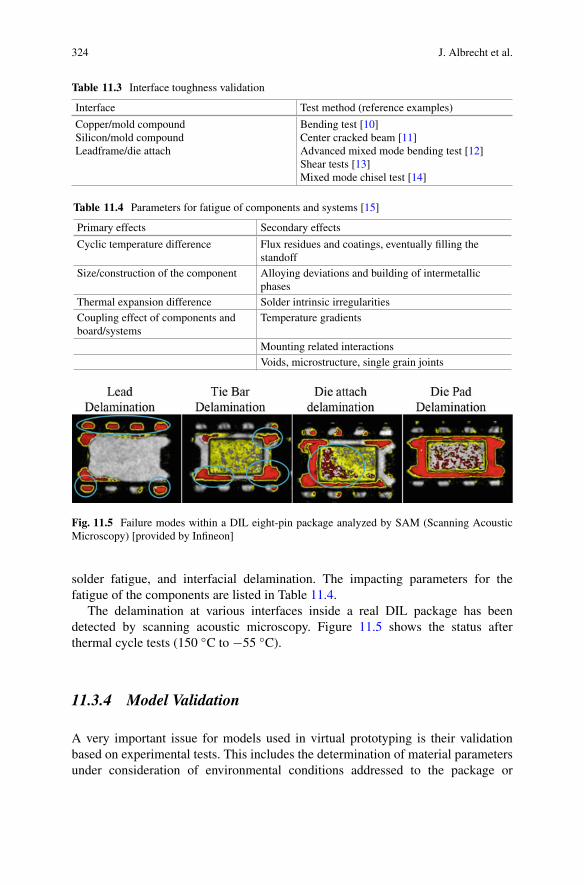
324 J. Albrecht et al.
Table 11.3 Interface toughness validation
Interface Test method (reference examples)
Copper/mold compoundSilicon/mold compoundLeadframe/die attach
Bending test [10]Center cracked beam [11]Advanced mixed mode bending test [12]Shear tests [13]Mixed mode chisel test [14]
Table 11.4 Parameters for fatigue of components and systems [15]
Primary effects Secondary effects
Cyclic temperature difference Flux residues and coatings, eventually filling thestandoff
Size/construction of the component Alloying deviations and building of intermetallicphases
Thermal expansion difference Solder intrinsic irregularitiesCoupling effect of components andboard/systems
Temperature gradients
Mounting related interactionsVoids, microstructure, single grain joints
Fig. 11.5 Failure modes within a DIL eight-pin package analyzed by SAM (Scanning AcousticMicroscopy) [provided by Infineon]
solder fatigue, and interfacial delamination. The impacting parameters for thefatigue of the components are listed in Table 11.4.
The delamination at various interfaces inside a real DIL package has beendetected by scanning acoustic microscopy. Figure 11.5 shows the status afterthermal cycle tests (150 ◦C to −55 ◦C).
11.3.4 Model Validation
A very important issue for models used in virtual prototyping is their validationbased on experimental tests. This includes the determination of material parametersunder consideration of environmental conditions addressed to the package or
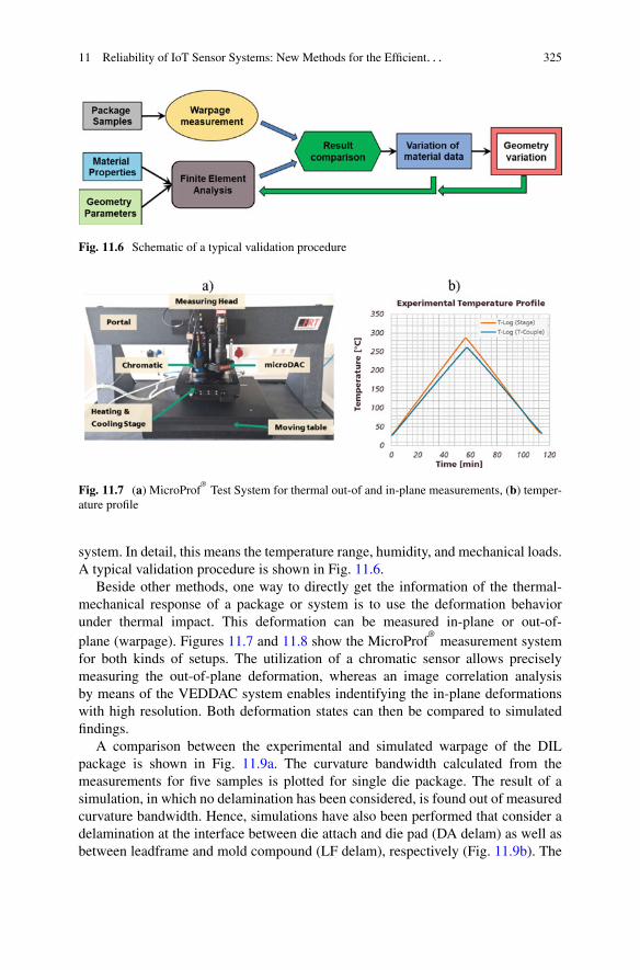
11 Reliability of IoT Sensor Systems: New Methods for the Efficient. . . 325
Fig. 11.6 Schematic of a typical validation procedure
Fig. 11.7 (a) MicroProf®
Test System for thermal out-of and in-plane measurements, (b) temper-ature profile
system. In detail, this means the temperature range, humidity, and mechanical loads.A typical validation procedure is shown in Fig. 11.6.
Beside other methods, one way to directly get the information of the thermal-mechanical response of a package or system is to use the deformation behaviorunder thermal impact. This deformation can be measured in-plane or out-of-plane (warpage). Figures 11.7 and 11.8 show the MicroProf
®measurement system
for both kinds of setups. The utilization of a chromatic sensor allows preciselymeasuring the out-of-plane deformation, whereas an image correlation analysisby means of the VEDDAC system enables indentifying the in-plane deformationswith high resolution. Both deformation states can then be compared to simulatedfindings.
A comparison between the experimental and simulated warpage of the DILpackage is shown in Fig. 11.9a. The curvature bandwidth calculated from themeasurements for five samples is plotted for single die package. The result of asimulation, in which no delamination has been considered, is found out of measuredcurvature bandwidth. Hence, simulations have also been performed that consider adelamination at the interface between die attach and die pad (DA delam) as well asbetween leadframe and mold compound (LF delam), respectively (Fig. 11.9b). The
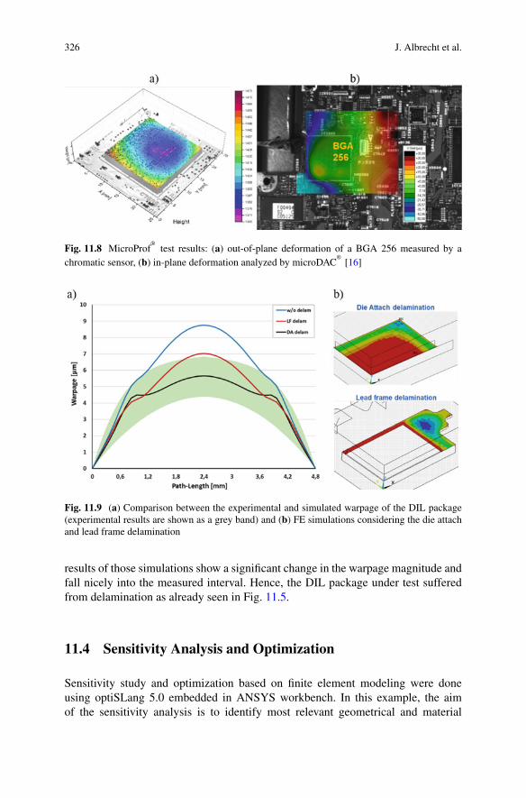
326 J. Albrecht et al.
Fig. 11.8 MicroProf®
test results: (a) out-of-plane deformation of a BGA 256 measured by achromatic sensor, (b) in-plane deformation analyzed by microDAC
®[16]
Fig. 11.9 (a) Comparison between the experimental and simulated warpage of the DIL package(experimental results are shown as a grey band) and (b) FE simulations considering the die attachand lead frame delamination
results of those simulations show a significant change in the warpage magnitude andfall nicely into the measured interval. Hence, the DIL package under test sufferedfrom delamination as already seen in Fig. 11.5.
11.4 Sensitivity Analysis and Optimization
Sensitivity study and optimization based on finite element modeling were doneusing optiSLang 5.0 embedded in ANSYS workbench. In this example, the aimof the sensitivity analysis is to identify most relevant geometrical and material
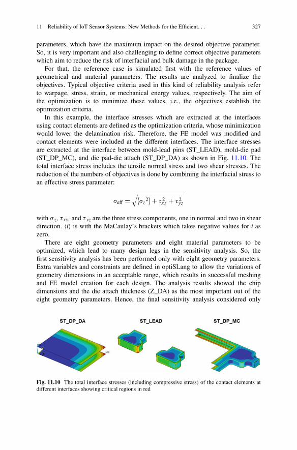
11 Reliability of IoT Sensor Systems: New Methods for the Efficient. . . 327
parameters, which have the maximum impact on the desired objective parameter.So, it is very important and also challenging to define correct objective parameterswhich aim to reduce the risk of interfacial and bulk damage in the package.
For that, the reference case is simulated first with the reference values ofgeometrical and material parameters. The results are analyzed to finalize theobjectives. Typical objective criteria used in this kind of reliability analysis referto warpage, stress, strain, or mechanical energy values, respectively. The aim ofthe optimization is to minimize these values, i.e., the objectives establish theoptimization criteria.
In this example, the interface stresses which are extracted at the interfacesusing contact elements are defined as the optimization criteria, whose minimizationwould lower the delamination risk. Therefore, the FE model was modified andcontact elements were included at the different interfaces. The interface stressesare extracted at the interface between mold-lead pins (ST_LEAD), mold-die pad(ST_DP_MC), and die pad-die attach (ST_DP_DA) as shown in Fig. 11.10. Thetotal interface stress includes the tensile normal stress and two shear stresses. Thereduction of the numbers of objectives is done by combining the interfacial stress toan effective stress parameter:
σeff =√⟨
σz2⟩+ τ 2
xz + τ 2yz
with σ z, τ xy, and τ yz are the three stress components, one in normal and two in sheardirection. 〈i〉 is with the MaCaulay’s brackets which takes negative values for i aszero.
There are eight geometry parameters and eight material parameters to beoptimized, which lead to many design legs in the sensitivity analysis. So, thefirst sensitivity analysis has been performed only with eight geometry parameters.Extra variables and constraints are defined in optiSLang to allow the variations ofgeometry dimensions in an acceptable range, which results in successful meshingand FE model creation for each design. The analysis results showed the chipdimensions and the die attach thickness (Z_DA) as the most important out of theeight geometry parameters. Hence, the final sensitivity analysis considered only
Fig. 11.10 The total interface stresses (including compressive stress) of the contact elements atdifferent interfaces showing critical regions in red
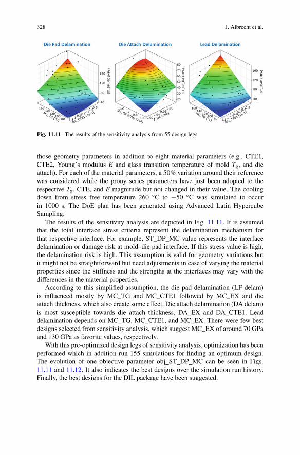
328 J. Albrecht et al.
Fig. 11.11 The results of the sensitivity analysis from 55 design legs
those geometry parameters in addition to eight material parameters (e.g., CTE1,CTE2, Young’s modulus E and glass transition temperature of mold Tg, and dieattach). For each of the material parameters, a 50% variation around their referencewas considered while the prony series parameters have just been adopted to therespective Tg, CTE, and E magnitude but not changed in their value. The coolingdown from stress free temperature 260 ◦C to −50 ◦C was simulated to occurin 1000 s. The DoE plan has been generated using Advanced Latin HypercubeSampling.
The results of the sensitivity analysis are depicted in Fig. 11.11. It is assumedthat the total interface stress criteria represent the delamination mechanism forthat respective interface. For example, ST_DP_MC value represents the interfacedelamination or damage risk at mold–die pad interface. If this stress value is high,the delamination risk is high. This assumption is valid for geometry variations butit might not be straightforward but need adjustments in case of varying the materialproperties since the stiffness and the strengths at the interfaces may vary with thedifferences in the material properties.
According to this simplified assumption, the die pad delamination (LF delam)is influenced mostly by MC_TG and MC_CTE1 followed by MC_EX and dieattach thickness, which also create some effect. Die attach delamination (DA delam)is most susceptible towards die attach thickness, DA_EX and DA_CTE1. Leaddelamination depends on MC_TG, MC_CTE1, and MC_EX. There were few bestdesigns selected from sensitivity analysis, which suggest MC_EX of around 70 GPaand 130 GPa as favorite values, respectively.
With this pre-optimized design legs of sensitivity analysis, optimization has beenperformed which in addition run 155 simulations for finding an optimum design.The evolution of one objective parameter obj_ST_DP_MC can be seen in Figs.11.11 and 11.12. It also indicates the best designs over the simulation run history.Finally, the best designs for the DIL package have been suggested.
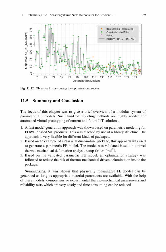
11 Reliability of IoT Sensor Systems: New Methods for the Efficient. . . 329
Fig. 11.12 Objective history during the optimization process
11.5 Summary and Conclusion
The focus of this chapter was to give a brief overview of a modular system ofparametric FE models. Such kind of modeling methods are highly needed forautomated virtual prototyping of current and future IoT solutions.
1. A fast model generation approach was shown based on parametric modeling forFOWLP based SiP products. This was reached by use of a library structure. Theapproach is very flexible for different kinds of packages.
2. Based on an example of a classical dual-in-line package, this approach was usedto generate a parametris FE model. The model was validated based on a novelthermo-mechanical defomation analysis setup (MicroProf
®).
3. Based on the validated parametric FE model, an optimization strategy wasfollowed to reduce the risk of thermo-mechanical driven delamination inside thepackage.
Summarizing, it was shown that physically meaningful FE model can begenerated as long as appropriate material parameters are available. With the helpof these models, comprehensive experimental thermo-mechanical assessments andreliability tests which are very costly and time consuming can be reduced.

330 J. Albrecht et al.
References
1. L.S.H. Lee et al., FOWLP technology as wafer level system in packaging (SiP) solution, in2017 International Conference on Electronics Packaging (ICEP), Yamagata, 2017, pp. 491–493
2. S. Rzepka, A. Müller, B. Michel, Virtual prototyping advanced by statistic and stochasticmethodologies, in 2010 11th International Thermal, Mechanical & Multi-Physics Simulation,and Experiments in Microelectronics and Microsystems (EuroSimE), Bordeaux, 2010, pp. 1–9
3. A.J. Przekwas, Y. Jiang, M.M. Athavale, Z.J. Wang, J. van der Zijp, A virtual prototypingenvironment for multi-scale, multi-disciplinary simulation of electronics packaging of MCMs,in InterSociety Conference on Thermal Phenomena in Electronic Systems, I-THERM V,Orlando, FL, 1996, pp. 352–358
4. J. Tang, P. Xi, B. Zhang, B. Hu, A finite element parametric modeling technique of aircraftwing structures. Chin. J. Aeronaut. 26(5), 1202–1210 (2013)., ISSN 1000-9361
5. J. Fan, Z. Yang, J. Wang, S. Ding, C. Liu, Z. Shi, Parametric finite element modelling andnonlinear analysis of vehicle brake, in 2009 International Conference on Mechatronics andAutomation, Changchun, 2009, pp. 1762–1766
6. A. Cardoso et al., Development of novel high density system integration solutions in FOWLP—complex and thin wafer-level SiP and wafer-level 3D packages, in IEEE 67th ElectronicComponents and Technology Conference, 2017, pp. 14–21
7. ANSYSTM, Multiphysics, Version 18, User’s Manual (Ansys Inc., 2018)8. G. Gadhiya, B. Brämer, S. Rzepka, Automated virtual prototyping for fastest time-to-market
of new system in package solutions, in 2018 7th Electronic System-Integration TechnologyConference (ESTC), Dresden, 2018, pp. 1–7
9. OptiSlang™, User Manual (Dynardo GmbH, Weimar, 2018)10. V. Sundararaman, B.D. Davidson, An unsymmetric double cantilever beam test for interfacial
fracture toughness determination. Int. J. Solids Struct. 34(7), 799–817 (1997)11. P.G. Charalambides, J. Lund, A.G. Evans, R.M. McMeeking, A test specimen for determining
the fracture resistance of bimaterial interfaces. J. Appl. Mech. 56(1), 77–82 (1989)12. J.R. Reeder, J.R. Crews Jr., Mixed-mode bending method for delamination testing. AIAA J.
28(7), 1270–1276 (1990)13. R. Dudek, B. Braemer, R. Pufall, H. Walter, B. Seiler, B. Wunderle, Determination of interface
fracture parameters by shear testing using different theoretical approaches, in Proc. 13thEuroSimE Conf., 2012
14. G. Schlottig, Reliability at the Chip interfaces: delaminating the silicon die from moldingcompound, Dissertation, 2012, ISBN: 978-94-6186-072-9
15. R. Dudek, Mounting effects on board level reliability, in EuWoRel-Workshop, Berlin, 201516. B. Seiler, R. Dudek, L. Scheiter, K. Kreyßig, S. Haase, Characterization of the Thermo-
Mechanical Deformation Behaviour of Composite Materials for Power Electronics UsingDigital Image Correlation Method microDAC
®, Micromaterials and Nanomaterials, 15, ISSN
1619-2486, MicroCar, 2013, pp. 204–207
Chapter 12Sensor Testing for Smart MobilityScenarios: From Parking Assistanceto Automated Parking
J. Murgoitio Larrauri, E. D. Martí Muñoz, M. E. Vaca Recalde, B. Hillbrand,A. Tengg, Ch. Pilz, and N. Druml
12.1 Introduction
At present, road vehicle automation is one of the major challenges of nowadays’transport system and its goals are to achieve the ideal energy efficiency, theminimum environment impact, and the highest safety rate as well as to improvethe drivers’ comfort. Due to this fact, currently, it is not only the trend to developsystems that help the driver in controlling the own vehicle in the driving processsuch as ADAS, but also Cooperative ITS for automating road transport as well.
These cooperative systems are based on communications in real time among IoTdevices. However, the connectivity between these devices and the vehicle, togetherwith the data obtained by the own vehicle, with the purpose to manage an automatedand adequate decision making, represents a new step in the evolution of this concept.
So, the concept of Internet of Vehicle (IoV) is the next step for future smarttransportation and mobility applications and requires creating a new IoT ecosystembased on trust, interoperability and security. IoT infrastructure (based on sensors,ubiquitous connectivity, information processing) will transform the environment
J. M. Larrauri (�) · E. D. M. Muñoz · M. E. V. RecaldeTecnalia Research & Innovation, Parque Científico y Tecnológico de Bizkaia, Derio, Bizkaia,Spaine-mail: [email protected]; [email protected]; [email protected]
B. Hillbrand · A. Tengg · C. PilzVirtual Vehicle Research Center, Graz, Austriae-mail: [email protected]; [email protected]; [email protected]
N. DrumlInfineon Technologies Austria AG, Graz, Austriae-mail: [email protected]
© Springer Nature Switzerland AG 2020W. D. van Driel et al. (eds.), Sensor Systems Simulations,https://doi.org/10.1007/978-3-030-16577-2_12
331
332 J. M. Larrauri et al.
and economics of mobility scenarios in the future: first through the connectionsand secondly through the emergence of an ecosystem of services around smartervehicles.
In this context, IoSense is the ECSEL project which will deploy new capabilities(Sensors, Components and Systems) through several demonstrators, one of themusing the SmaBility use cases: The connection of vehicles to their surroundingenvironment and to Internet will offer a great variety of new possibilities that willbring new functionality to citizen and organizations and will make the transportmore efficient and safer. Intelligent perception and decision making for saferand autonomous driving are the main objectives of the SmaBility demonstrators,which clearly search for safer driving and new application ecosystem associated tomobility: Automated parking is one of the Smability use cases.
The called “Automated parking” IoSense SmaBility use case impacts the mobil-ity application domain by enabling and advancing concepts for Internet of Vehicle(IoV) as the next step for future smart transportation and mobility applicationscreating a new IoT ecosystem based on trust, interoperability and security. Thisdemonstrator of the IoT use case enables a significant progress beyond the state-of-the-art on high performance information processing through data fusion algorithmsthat combine V2V and V2I information with on-board sensor information.
The results of this demonstrator will accomplish the MASP defined in the [1].It will be built on advanced systems for driver assistance, cooperative systems,and driver status monitoring as well as environment perception. Systems willbe validated under virtual, semi-virtual and real-world conditions (i.e. weatherconditions). This requires dependable solutions for advanced sensors and actuators,data fusion, efficient use of connectivity human interaction technologies, CPS, and(real-time) simulation concepts.
This chapter is structured by the following sections:
• Introduction• Selection of adequate simulation methodologies• TOF-Concept and design of sensors system• Simulation model development: Simulation elements, Algorithms, and Testing• Summary and conclusions
12.2 Selection of Adequate Simulation Methodologies
This chapter lists the capabilities in the design, modelling and simulation area ofeach partner (TECNALIA, IFAT and VIF) involved on the title “From ParkingAssistance to Automated Parking” within the Smart Mobility scenarios (Smability).
12 Sensor Testing for Smart Mobility Scenarios: From Parking Assistance. . . 333
12.2.1 Tecnalia
Tecnalia, as a research company with around 1500 workers, most of them engineers,uses different simulation tools. Anyway, the department involved on this project isfocused on intelligent transport systems, and more specifically we are interestedon smart mobility scenarios using ADAS systems and automated ground vehicles(UGV).
From this point of view, vehicle simulators are very valuable for validation andtesting of new functionalities for automated driving. In order to increase securityand safety in new algorithms, realistic simulators are necessary in the automotivesector.
From partially automated to fully automated systems (SAE J3016 levels), someof the key components are communicated between the different on-board elements(perception, human interaction and control algorithms). In this sense, a simulatorthat combined all these features to reduce the real test effort is very convenient.In the last decades, the relationship between control algorithm development andsystem dynamics implementation is increasing. In order to develop better decisionand control features for automated vehicles, a precise multi-body model to describethe vehicle dynamics in different scenarios is still missing.
Robust dynamic models, based on a correct environment modelling, are going tolead a reduction of development cost of the new ADAS. In this section, a descriptionof the current simulator available on market used by us is presented.
12.2.1.1 Civitec Pro-Sivic
This tool has been designed as a sensor simulator by the company CIVITEC. Itgives the opportunity to simulate a variety of complex scenarios like intersections,roundabouts, multiple vehicles and pedestrians on the road, and changes in theweather conditions rain, fog, snow, brightness and others.
Moreover, it allows to adapt the parameters and behaviours of sensors andweather, and it has the potential of being connected with RTMaps platform to testnew algorithms, from the data fusion and control point of view.
There are some technologies that have been tested on this platform on lastyears. Real-time road lane detection and tracking is one most interesting. Anotherapplication is the use of the platform Simulink/Matlab to communicate it withthe Pro-SIVIC simulator to test cooperative algorithms, like CACC (CooperativeAdaptive Cruise Control), on automated vehicles. Pro-Sivic is mainly oriented toperception and ADAS developments.
12.2.1.2 CarSim and TruckSim
CarSim and TruckSim are products of the Mechanical Simulation Company, thoseare dynamics vehicle simulators, for passenger cars and light trucks, respectively.
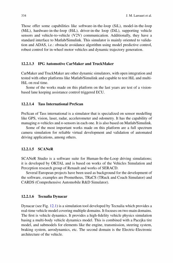
334 J. M. Larrauri et al.
Those offer some capabilities like software-in-the-loop (SiL), model-in-the-loop(MiL), hardware-in-the-loop (HiL), driver-in-the loop (DiL), supporting vehiclesensors and vehicle-to-vehicle (V2V) communication. Additionally, they have astandard interface to Matlab/Simulink. This simulator is mainly oriented to valida-tion and ADAS, i.e.: obstacle avoidance algorithm using model predictive control,robust control for in-wheel motor vehicles and dynamic trajectory generation.
12.2.1.3 IPG Automotive CarMaker and TruckMaker
CarMaker and TruckMaker are other dynamic simulators, with open integration andtested with other platforms like Matlab/Simulink and capable to test HiL and multi-HiL on real time.
Some of the works made on this platform on the last years are test of a vision-based lane keeping assistance control triggered ECU.
12.2.1.4 Tass International PreScan
PreScan of Tass international is a simulator that is specialized on sensor modellinglike GPS, vision, laser, radar, accelerometer and odometry. It has the capability ofmanaging n-vehicles and n-sensors in each one. It is also based on Matlab/Simulink.
Some of the most important works made on this platform are a full spectrumcamera simulation for reliable virtual development and validation of automateddriving applications, among others.
12.2.1.5 SCANeR
SCANeR Studio is a software suite for Human-In-the-Loop driving simulations;it is developed by OKTAL and is based on works of the Vehicles Simulation andPerception research group of Renault and works of SERACD.
Several European projects have been used as background for the development ofthe software, examples are Prometheus, TRaCS (TRuck and Coach Simulator) andCARDS (Comprehensive Automobile R&D Simulator).
12.2.1.6 Tecnalia Dynacar
Dynacar (see Fig. 12.1) is a simulation tool developed by Tecnalia which provides areal-time vehicle model covering multiple domains. It focuses on two main domains.The first is vehicle dynamics. It provides a high-fidelity vehicle physics simulationbasing a multi-body vehicle dynamics model. This is combined with a Pacejka tiremodel, and submodels for elements like the engine, transmission, steering system,braking system, aerodynamics, etc. The second domain is the Electric-Electronicarchitecture of the vehicle.
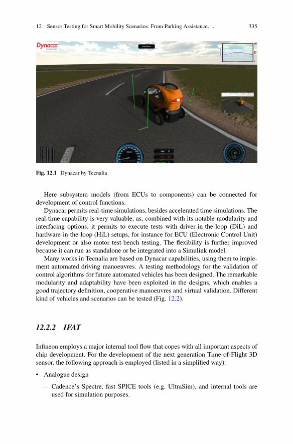
12 Sensor Testing for Smart Mobility Scenarios: From Parking Assistance. . . 335
Fig. 12.1 Dynacar by Tecnalia
Here subsystem models (from ECUs to components) can be connected fordevelopment of control functions.
Dynacar permits real-time simulations, besides accelerated time simulations. Thereal-time capability is very valuable, as, combined with its notable modularity andinterfacing options, it permits to execute tests with driver-in-the-loop (DiL) andhardware-in-the-loop (HiL) setups, for instance for ECU (Electronic Control Unit)development or also motor test-bench testing. The flexibility is further improvedbecause it can run as standalone or be integrated into a Simulink model.
Many works in Tecnalia are based on Dynacar capabilities, using them to imple-ment automated driving manoeuvres. A testing methodology for the validation ofcontrol algorithms for future automated vehicles has been designed. The remarkablemodularity and adaptability have been exploited in the designs, which enables agood trajectory definition, cooperative manoeuvres and virtual validation. Differentkind of vehicles and scenarios can be tested (Fig. 12.2).
12.2.2 IFAT
Infineon employs a major internal tool flow that copes with all important aspects ofchip development. For the development of the next generation Time-of-Flight 3Dsensor, the following approach is employed (listed in a simplified way):
• Analogue design
– Cadence’s Spectre, fast SPICE tools (e.g. UltraSim), and internal tools areused for simulation purposes.
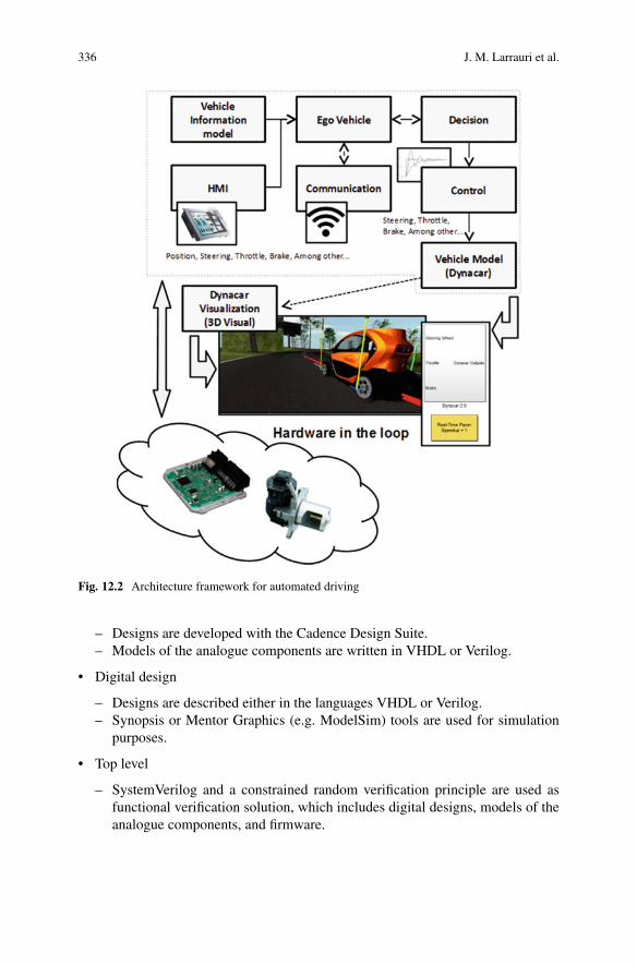
336 J. M. Larrauri et al.
Fig. 12.2 Architecture framework for automated driving
– Designs are developed with the Cadence Design Suite.– Models of the analogue components are written in VHDL or Verilog.
• Digital design
– Designs are described either in the languages VHDL or Verilog.– Synopsis or Mentor Graphics (e.g. ModelSim) tools are used for simulation
purposes.
• Top level
– SystemVerilog and a constrained random verification principle are used asfunctional verification solution, which includes digital designs, models of theanalogue components, and firmware.
12 Sensor Testing for Smart Mobility Scenarios: From Parking Assistance. . . 337
• System level
– Matlab is used as the most important tool to model and simulate Time-of-Flight camera system concepts (sensor + illumination unit).
12.2.3 Virtual Vehicle (VIF)
In the past few decades, numerous specific simulation tools have been establishedin the automotive industry. However, these tools typically specialize on individualareas of expertise. There is very limited support for a heterogeneous simulationenvironment. The goal of “co-simulation” is to overcome this limitation and tomerge the challenges from different areas. Common co-simulation platforms areoften limited to a single area of expertise (e.g. the design of a thermal managementsystem with a heterogeneous tool landscape). Such platforms typically addressproblems from a very specific, restricted dynamic range, which means that thedifferent models exhibit similar time behaviour.
However, the development of modern, mechatronic systems requires a muchbroader approach. The interactions between sub-systems from different areas haveto be taken into account through a suitable interconnection of the parts. The couplingof existing (specific) simulation programmes (and the models implemented therein)from different areas of expertise represents a promising approach for the simulationof the complete system.
With the introduction of co-simulation in the development process, the task ofdeveloping complex mechatronic systems can be solved in a very efficient way.For example, the integration of Finite Element Methods (FEM) is supported forapplications in the field of “Integral Safety”. Another example is the integrationof electrical and thermal components into existing drivetrain concepts in the field of“alternative drives”, such as hybrid or electric vehicles. In all of these considerationsthe vehicle itself is not the exclusive focus, but rather the interactions with thevehicle’s environment and the influence of the real driver are taken into account.
The task of a co-simulation platform is to take the complex interactions of thevarious simulation models in a suitable and correct way into account. The platformhas to enable the precise co-working of different simulation tools.
The co-simulation platform ICOS (Independent Co-Simulation; see [2]) devel-oped at VIF fulfils all these requirements (Fig. 12.3). Over the past years, ICOS hasproven both its flexibility and its reliability to succeed in a vast amount of differentautomotive use cases. ICOS is included in the software AVL Model.CONNECT™1.Apart from a user-friendly graphical interface, Model.CONNECT™ offers powerfulmodel integration capabilities as well as an efficient post-processing and visualiza-tion engine.
1The Model.CONNECT™ software suite is distributed by AVL. For research projects—likeIoSense—VIF can provide licenses free of charge but limited to the project duration and projectcontent.
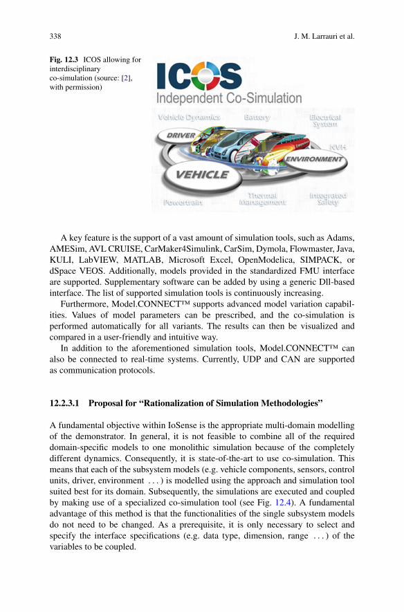
338 J. M. Larrauri et al.
Fig. 12.3 ICOS allowing forinterdisciplinaryco-simulation (source: [2],with permission)
A key feature is the support of a vast amount of simulation tools, such as Adams,AMESim, AVL CRUISE, CarMaker4Simulink, CarSim, Dymola, Flowmaster, Java,KULI, LabVIEW, MATLAB, Microsoft Excel, OpenModelica, SIMPACK, ordSpace VEOS. Additionally, models provided in the standardized FMU interfaceare supported. Supplementary software can be added by using a generic Dll-basedinterface. The list of supported simulation tools is continuously increasing.
Furthermore, Model.CONNECT™ supports advanced model variation capabil-ities. Values of model parameters can be prescribed, and the co-simulation isperformed automatically for all variants. The results can then be visualized andcompared in a user-friendly and intuitive way.
In addition to the aforementioned simulation tools, Model.CONNECT™ canalso be connected to real-time systems. Currently, UDP and CAN are supportedas communication protocols.
12.2.3.1 Proposal for “Rationalization of Simulation Methodologies”
A fundamental objective within IoSense is the appropriate multi-domain modellingof the demonstrator. In general, it is not feasible to combine all of the requireddomain-specific models to one monolithic simulation because of the completelydifferent dynamics. Consequently, it is state-of-the-art to use co-simulation. Thismeans that each of the subsystem models (e.g. vehicle components, sensors, controlunits, driver, environment . . . ) is modelled using the approach and simulation toolsuited best for its domain. Subsequently, the simulations are executed and coupledby making use of a specialized co-simulation tool (see Fig. 12.4). A fundamentaladvantage of this method is that the functionalities of the single subsystem modelsdo not need to be changed. As a prerequisite, it is only necessary to select andspecify the interface specifications (e.g. data type, dimension, range . . . ) of thevariables to be coupled.
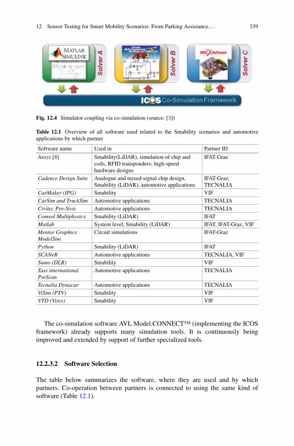
12 Sensor Testing for Smart Mobility Scenarios: From Parking Assistance. . . 339
Fig. 12.4 Simulator coupling via co-simulation (source: [3])
Table 12.1 Overview of all software used related to the Smability scenarios and automotiveapplications by which partner
Software name Used in Partner ID
Ansys [8] Smability(LiDAR), simulation of chip andcoils, RFID transponders; high-speedhardware designs
IFAT-Graz
Cadence Design Suite Analogue and mixed-signal chip design,Smability (LiDAR), automotive applications
IFAT-Graz,TECNALIA
CarMaker (IPG) Smability VIFCarSim and TruckSim Automotive applications TECNALIACivitec Pro-Sivic Automotive applications TECNALIAComsol Multiphysics Smability (LiDAR) IFATMatlab System level, Smability (LiDAR) IFAT, IFAT-Graz, VIFMentor GraphicsModelSim
Circuit simulations IFAT-Graz
Python Smability (LiDAR) IFATSCANeR Automotive applications TECNALIA, VIFSumo (DLR) Smability VIFTass internationalPreScan
Automotive applications TECNALIA
Tecnalia Dynacar Automotive applications TECNALIAViSim (PTV) Smability VIFVTD (Vires) Smability VIF
The co-simulation software AVL Model.CONNECT™ (implementing the ICOSframework) already supports many simulation tools. It is continuously beingimproved and extended by support of further specialized tools.
12.2.3.2 Software Selection
The table below summarizes the software, where they are used and by whichpartners. Co-operation between partners is connected to using the same kind ofsoftware (Table 12.1).
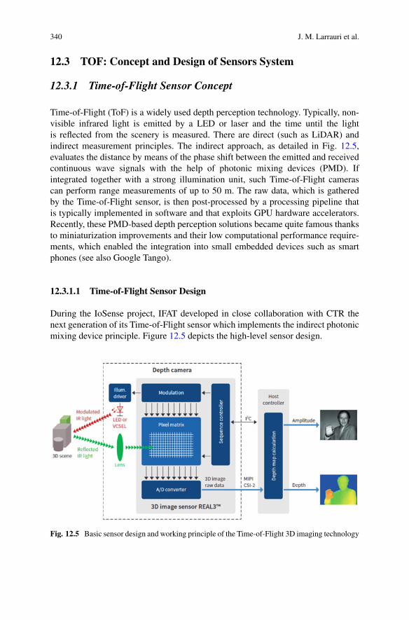
340 J. M. Larrauri et al.
12.3 TOF: Concept and Design of Sensors System
12.3.1 Time-of-Flight Sensor Concept
Time-of-Flight (ToF) is a widely used depth perception technology. Typically, non-visible infrared light is emitted by a LED or laser and the time until the lightis reflected from the scenery is measured. There are direct (such as LiDAR) andindirect measurement principles. The indirect approach, as detailed in Fig. 12.5,evaluates the distance by means of the phase shift between the emitted and receivedcontinuous wave signals with the help of photonic mixing devices (PMD). Ifintegrated together with a strong illumination unit, such Time-of-Flight camerascan perform range measurements of up to 50 m. The raw data, which is gatheredby the Time-of-Flight sensor, is then post-processed by a processing pipeline thatis typically implemented in software and that exploits GPU hardware accelerators.Recently, these PMD-based depth perception solutions became quite famous thanksto miniaturization improvements and their low computational performance require-ments, which enabled the integration into small embedded devices such as smartphones (see also Google Tango).
12.3.1.1 Time-of-Flight Sensor Design
During the IoSense project, IFAT developed in close collaboration with CTR thenext generation of its Time-of-Flight sensor which implements the indirect photonicmixing device principle. Figure 12.5 depicts the high-level sensor design.
Fig. 12.5 Basic sensor design and working principle of the Time-of-Flight 3D imaging technology
12 Sensor Testing for Smart Mobility Scenarios: From Parking Assistance. . . 341
• An I2C interface is used to configure and control the sensor. Lots of registers,within a dedicated register container, are implemented in order to enable highflexibility and to support various types of applications (such as 3D scanning,gesture recognition, driver monitoring).
• A small sized and power-efficient internal controller is used to control the sensorSoC and its components. This proprietary controller developed by Infineonfeatures not only modulation control, illumination control, pixel actuation, butalso supports autonomous imaging phase sequences (such as combination offour-phase Time-of-Flight measurements used for gesture recognition with eight-or nine-phase Time-of-Flight measurements used e.g. by Google Tango) or codedmodulation.
• The modulation and phase shifter component is one of the central elements of thesensor. Typically, one Time-of-Flight measurement requires shifting the phaseof the emitted light several times (e.g. four times). Therefore, the modulationand phase shifter component implement a lot of complex logic. Furthermore,this block will support the innovative approach of coded modulation, which willdrastically boost the performance of the next generation sensor.
• An illumination driver is implemented in order to emit modulated infrared lightwith the help of an external LED or VCSEL (laser).
• As shown in Fig. 12.5, after emitting modulated infrared light, the reflected lightis focused by several lenses onto the PMD pixel matrix. Since PMD pixels arelarger than RGB pixels, the light sensitive area of each pixel is consequentlysmaller. This smaller fill-factor results in reduced efficiency in converting lightto electrons. This drawback is addressed by implementing micro-lenses on top ofeach pixel in order to focus the incoming light to the pixel’s light sensitive area.
• High-speed A/D converters read out the pixels and transform their raw analoguevalues into the digital domain.
• Finally, a high-speed CSI-2 serial interface is used to transmit the sensor data tothe application processor. Thanks to this standardized interface, the sensor canbe easily integrated into small embedded systems such as smart phones.
IFAT’s and CTR’s activities not only fully addressed IoSense’s objectives ofreducing sensor manufacturing costs and sensor manufacturing time, the partnersfully strived for improving sensor performance (e.g. in terms of power consumption)and measurement accuracy. These objectives lead to the following exemplifiedconceptual and design improvements developed during IoSense:
• The sensor’s chip area is shrunk by more than 30% which consequently reducesmanufacturing costs and improves the yield. Furthermore, an improved yield alsoimproves margins accordingly.
• Given the fact that the Time-of-Flight sensor implements a rather complexoptical measurement principle, also wafer-level testing is more complex than thetesting of standard CMOS RGB sensors. Because test time directly influencesthe costs, it is of high importance to integrate sufficient test capabilities and thusto reduce test times as much as possible. Therefore, the next generation Time-
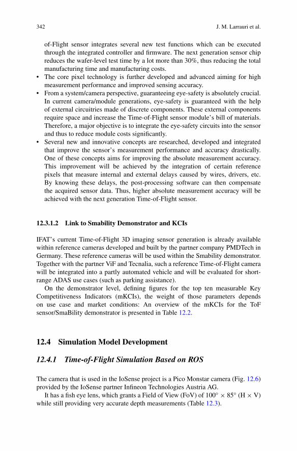
342 J. M. Larrauri et al.
of-Flight sensor integrates several new test functions which can be executedthrough the integrated controller and firmware. The next generation sensor chipreduces the wafer-level test time by a lot more than 30%, thus reducing the totalmanufacturing time and manufacturing costs.
• The core pixel technology is further developed and advanced aiming for highmeasurement performance and improved sensing accuracy.
• From a system/camera perspective, guaranteeing eye-safety is absolutely crucial.In current camera/module generations, eye-safety is guaranteed with the helpof external circuitries made of discrete components. These external componentsrequire space and increase the Time-of-Flight sensor module’s bill of materials.Therefore, a major objective is to integrate the eye-safety circuits into the sensorand thus to reduce module costs significantly.
• Several new and innovative concepts are researched, developed and integratedthat improve the sensor’s measurement performance and accuracy drastically.One of these concepts aims for improving the absolute measurement accuracy.This improvement will be achieved by the integration of certain referencepixels that measure internal and external delays caused by wires, drivers, etc.By knowing these delays, the post-processing software can then compensatethe acquired sensor data. Thus, higher absolute measurement accuracy will beachieved with the next generation Time-of-Flight sensor.
12.3.1.2 Link to Smability Demonstrator and KCIs
IFAT’s current Time-of-Flight 3D imaging sensor generation is already availablewithin reference cameras developed and built by the partner company PMDTech inGermany. These reference cameras will be used within the Smability demonstrator.Together with the partner ViF and Tecnalia, such a reference Time-of-Flight camerawill be integrated into a partly automated vehicle and will be evaluated for short-range ADAS use cases (such as parking assistance).
On the demonstrator level, defining figures for the top ten measurable KeyCompetitiveness Indicators (mKCIs), the weight of those parameters dependson use case and market conditions: An overview of the mKCIs for the ToFsensor/SmaBility demonstrator is presented in Table 12.2.
12.4 Simulation Model Development
12.4.1 Time-of-Flight Simulation Based on ROS
The camera that is used in the IoSense project is a Pico Monstar camera (Fig. 12.6)provided by the IoSense partner Infineon Technologies Austria AG.
It has a fish eye lens, which grants a Field of View (FoV) of 100◦ × 85◦ (H × V)while still providing very accurate depth measurements (Table 12.3).
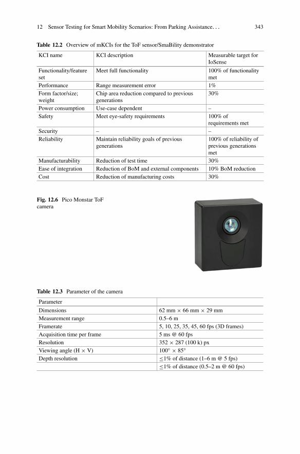
12 Sensor Testing for Smart Mobility Scenarios: From Parking Assistance. . . 343
Table 12.2 Overview of mKCIs for the ToF sensor/SmaBility demonstrator
KCI name KCI description Measurable target forIoSense
Functionality/featureset
Meet full functionality 100% of functionalitymet
Performance Range measurement error 1%Form factor/size;weight
Chip area reduction compared to previousgenerations
30%
Power consumption Use-case dependent –Safety Meet eye-safety requirements 100% of
requirements metSecurity – –Reliability Maintain reliability goals of previous
generations100% of reliability ofprevious generationsmet
Manufacturability Reduction of test time 30%Ease of integration Reduction of BoM and external components 10% BoM reductionCost Reduction of manufacturing costs 30%
Fig. 12.6 Pico Monstar ToFcamera
Table 12.3 Parameter of the camera
Parameter
Dimensions 62 mm × 66 mm × 29 mmMeasurement range 0.5–6 mFramerate 5, 10, 25, 35, 45, 60 fps (3D frames)Acquisition time per frame 5 ms @ 60 fpsResolution 352 × 287 (100 k) pxViewing angle (H × V) 100◦ × 85◦Depth resolution ≤1% of distance (1–6 m @ 5 fps)
≤1% of distance (0.5–2 m @ 60 fps)
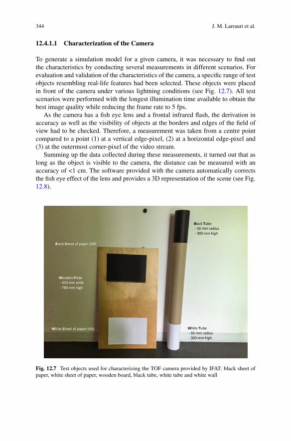
344 J. M. Larrauri et al.
12.4.1.1 Characterization of the Camera
To generate a simulation model for a given camera, it was necessary to find outthe characteristics by conducting several measurements in different scenarios. Forevaluation and validation of the characteristics of the camera, a specific range of testobjects resembling real-life features had been selected. These objects were placedin front of the camera under various lightning conditions (see Fig. 12.7). All testscenarios were performed with the longest illumination time available to obtain thebest image quality while reducing the frame rate to 5 fps.
As the camera has a fish eye lens and a frontal infrared flash, the derivation inaccuracy as well as the visibility of objects at the borders and edges of the field ofview had to be checked. Therefore, a measurement was taken from a centre pointcompared to a point (1) at a vertical edge-pixel, (2) at a horizontal edge-pixel and(3) at the outermost corner-pixel of the video stream.
Summing up the data collected during these measurements, it turned out that aslong as the object is visible to the camera, the distance can be measured with anaccuracy of <1 cm. The software provided with the camera automatically correctsthe fish eye effect of the lens and provides a 3D representation of the scene (see Fig.12.8).
Fig. 12.7 Test objects used for characterizing the TOF camera provided by IFAT: black sheet ofpaper, white sheet of paper, wooden board, black tube, white tube and white wall
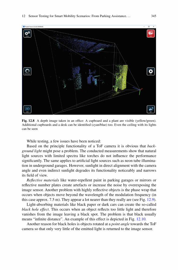
12 Sensor Testing for Smart Mobility Scenarios: From Parking Assistance. . . 345
Fig. 12.8 A depth image taken in an office: A cupboard and a plant are visible (yellow/green).Additional cupboards and a desk can be identified (cyan/blue) too. Even the ceiling with its lightscan be seen
While testing, a few issues have been noticed:Based on the principle functionality of a ToF camera it is obvious that back-
ground light might pose a problem. The conducted measurements show that naturallight sources with limited spectra like torches do not influence the performancesignificantly. The same applies to artificial light sources such as neon tube illumina-tion in underground garages. However, sunlight in direct alignment with the cameraangle and even indirect sunlight degrades its functionality noticeably and narrowsits field of view.
Reflective materials like water-repellent paint in parking garages or mirrors orreflective number plates create artefacts or increase the noise by overexposing theimage sensor. Another problem with highly reflective objects is the phase wrap thatoccurs when objects move beyond the wavelength of the modulation frequency (inthis case approx. 7.5 m). They appear a lot nearer than they really are (see Fig. 12.9).
Light-absorbing materials like black paper or dark cars can create the so-calledblack hole effect. This occurs when an object reflects too little light and thereforevanishes from the image leaving a black spot. The problem is that black usuallymeans “infinite distance”. An example of this effect is depicted in Fig. 12.10.
Another reason for black holes is objects rotated at a point angle towards the ToFcamera so that only very little of the emitted light is returned to the image sensor.
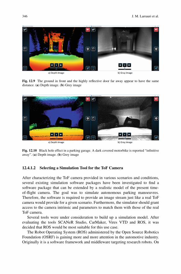
346 J. M. Larrauri et al.
Fig. 12.9 The ground in front and the highly reflective door far away appear to have the samedistance. (a) Depth image. (b) Grey image
Fig. 12.10 Black hole effect in a parking garage. A dark covered motorbike is reported “infinitiveaway”. (a) Depth image. (b) Grey image
12.4.1.2 Selecting a Simulation Tool for the ToF Camera
After characterizing the ToF camera provided in various scenarios and conditions,several existing simulation software packages have been investigated to find asoftware package that can be extended by a realistic model of the present time-of-flight camera. The goal was to simulate autonomous parking manoeuvres.Therefore, the software is required to provide an image stream just like a real ToFcamera would provide for a given scenario. Furthermore, the simulator should grantaccess to the camera intrinsic and parameters to match them with those of the realToF camera.
Several tools were under consideration to build up a simulation model. Afterevaluating the tools SCANeR Studio, CarMaker, Vires VTD and ROS, it wasdecided that ROS would be most suitable for this use case.
The Robot Operating System (ROS) administered by the Open Source RoboticsFoundation (OSRF) is gaining more and more attention in the automotive industry.Originally it is a software framework and middleware targeting research robots. On
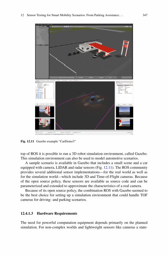
12 Sensor Testing for Smart Mobility Scenarios: From Parking Assistance. . . 347
Fig. 12.11 Gazebo example “CarDemo3”
top of ROS it is possible to run a 3D robot simulation environment, called Gazebo.This simulation environment can also be used to model automotive scenarios.
A sample scenario is available in Gazebo that includes a small scene and a carequipped with camera, LIDAR and radar sensors (Fig. 12.11). The ROS communityprovides several additional sensor implementations—for the real world as well asfor the simulation world—which include 3D and Time-of-Flight cameras. Becauseof the open source policy, these sensors are available as source code and can beparameterized and extended to approximate the characteristics of a real camera.
Because of its open source policy, the combination ROS with Gazebo seemed tobe the best choice for setting up a simulation environment that could handle TOFcameras for driving- and parking scenarios.
12.4.1.3 Hardware Requirements
The need for powerful computation equipment depends primarily on the plannedsimulation. For non-complex worlds and lightweight sensors like cameras a state-
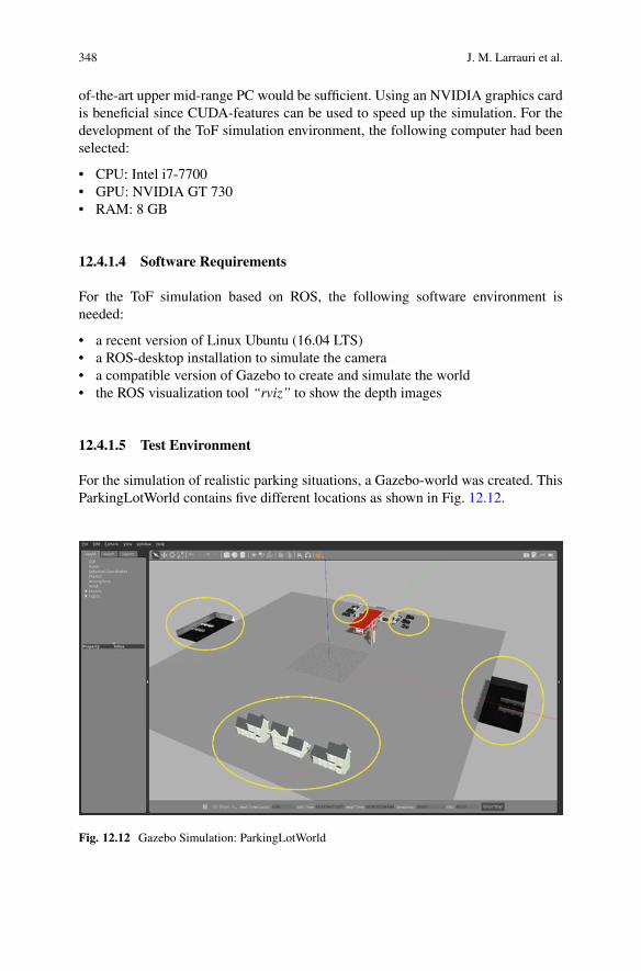
348 J. M. Larrauri et al.
of-the-art upper mid-range PC would be sufficient. Using an NVIDIA graphics cardis beneficial since CUDA-features can be used to speed up the simulation. For thedevelopment of the ToF simulation environment, the following computer had beenselected:
• CPU: Intel i7-7700• GPU: NVIDIA GT 730• RAM: 8 GB
12.4.1.4 Software Requirements
For the ToF simulation based on ROS, the following software environment isneeded:
• a recent version of Linux Ubuntu (16.04 LTS)• a ROS-desktop installation to simulate the camera• a compatible version of Gazebo to create and simulate the world• the ROS visualization tool “rviz” to show the depth images
12.4.1.5 Test Environment
For the simulation of realistic parking situations, a Gazebo-world was created. ThisParkingLotWorld contains five different locations as shown in Fig. 12.12.
Fig. 12.12 Gazebo Simulation: ParkingLotWorld
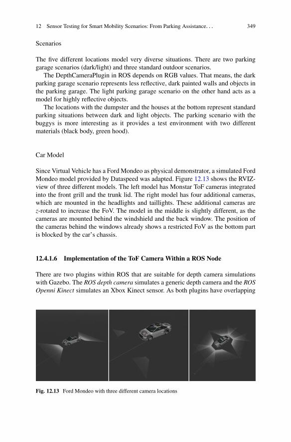
12 Sensor Testing for Smart Mobility Scenarios: From Parking Assistance. . . 349
Scenarios
The five different locations model very diverse situations. There are two parkinggarage scenarios (dark/light) and three standard outdoor scenarios.
The DepthCameraPlugin in ROS depends on RGB values. That means, the darkparking garage scenario represents less reflective, dark painted walls and objects inthe parking garage. The light parking garage scenario on the other hand acts as amodel for highly reflective objects.
The locations with the dumpster and the houses at the bottom represent standardparking situations between dark and light objects. The parking scenario with thebuggys is more interesting as it provides a test environment with two differentmaterials (black body, green hood).
Car Model
Since Virtual Vehicle has a Ford Mondeo as physical demonstrator, a simulated FordMondeo model provided by Dataspeed was adapted. Figure 12.13 shows the RVIZ-view of three different models. The left model has Monstar ToF cameras integratedinto the front grill and the trunk lid. The right model has four additional cameras,which are mounted in the headlights and taillights. These additional cameras arez-rotated to increase the FoV. The model in the middle is slightly different, as thecameras are mounted behind the windshield and the back window. The position ofthe cameras behind the windows already shows a restricted FoV as the bottom partis blocked by the car’s chassis.
12.4.1.6 Implementation of the ToF Camera Within a ROS Node
There are two plugins within ROS that are suitable for depth camera simulationswith Gazebo. The ROS depth camera simulates a generic depth camera and the ROSOpenni Kinect simulates an Xbox Kinect sensor. As both plugins have overlapping
Fig. 12.13 Ford Mondeo with three different camera locations
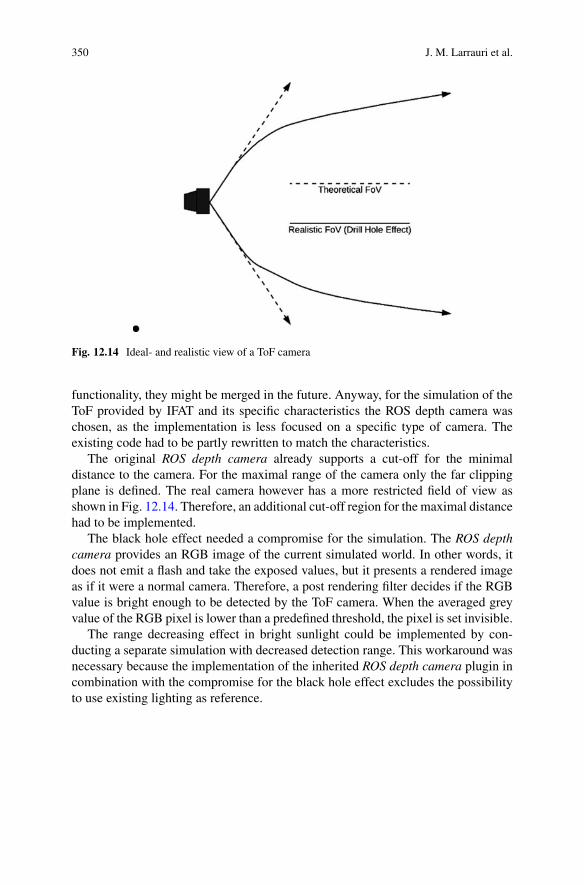
350 J. M. Larrauri et al.
Fig. 12.14 Ideal- and realistic view of a ToF camera
functionality, they might be merged in the future. Anyway, for the simulation of theToF provided by IFAT and its specific characteristics the ROS depth camera waschosen, as the implementation is less focused on a specific type of camera. Theexisting code had to be partly rewritten to match the characteristics.
The original ROS depth camera already supports a cut-off for the minimaldistance to the camera. For the maximal range of the camera only the far clippingplane is defined. The real camera however has a more restricted field of view asshown in Fig. 12.14. Therefore, an additional cut-off region for the maximal distancehad to be implemented.
The black hole effect needed a compromise for the simulation. The ROS depthcamera provides an RGB image of the current simulated world. In other words, itdoes not emit a flash and take the exposed values, but it presents a rendered imageas if it were a normal camera. Therefore, a post rendering filter decides if the RGBvalue is bright enough to be detected by the ToF camera. When the averaged greyvalue of the RGB pixel is lower than a predefined threshold, the pixel is set invisible.
The range decreasing effect in bright sunlight could be implemented by con-ducting a separate simulation with decreased detection range. This workaround wasnecessary because the implementation of the inherited ROS depth camera plugin incombination with the compromise for the black hole effect excludes the possibilityto use existing lighting as reference.
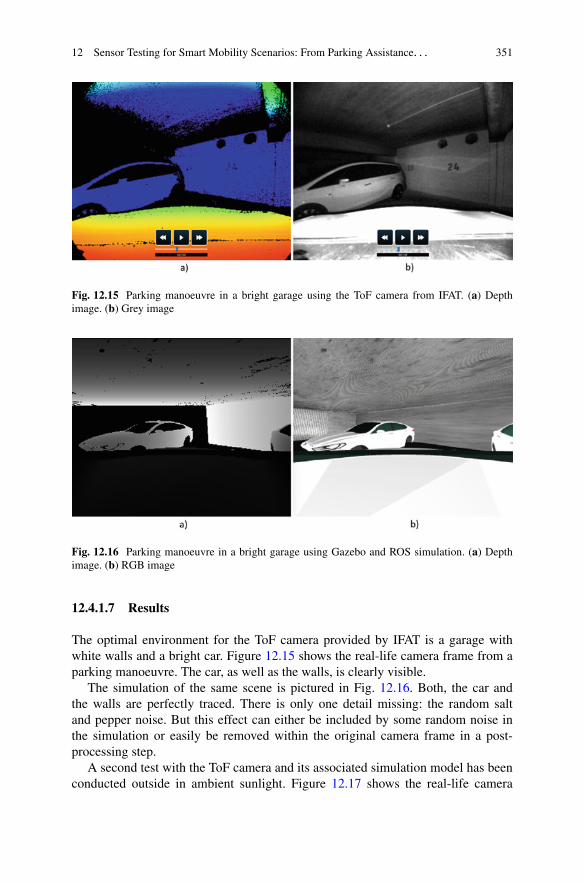
12 Sensor Testing for Smart Mobility Scenarios: From Parking Assistance. . . 351
Fig. 12.15 Parking manoeuvre in a bright garage using the ToF camera from IFAT. (a) Depthimage. (b) Grey image
Fig. 12.16 Parking manoeuvre in a bright garage using Gazebo and ROS simulation. (a) Depthimage. (b) RGB image
12.4.1.7 Results
The optimal environment for the ToF camera provided by IFAT is a garage withwhite walls and a bright car. Figure 12.15 shows the real-life camera frame from aparking manoeuvre. The car, as well as the walls, is clearly visible.
The simulation of the same scene is pictured in Fig. 12.16. Both, the car andthe walls are perfectly traced. There is only one detail missing: the random saltand pepper noise. But this effect can either be included by some random noise inthe simulation or easily be removed within the original camera frame in a post-processing step.
A second test with the ToF camera and its associated simulation model has beenconducted outside in ambient sunlight. Figure 12.17 shows the real-life camera
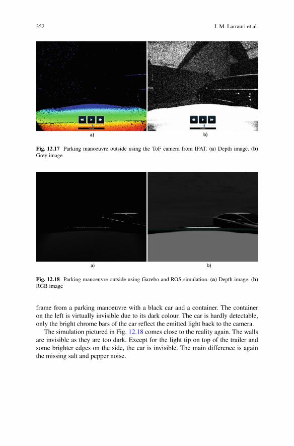
352 J. M. Larrauri et al.
Fig. 12.17 Parking manoeuvre outside using the ToF camera from IFAT. (a) Depth image. (b)Grey image
Fig. 12.18 Parking manoeuvre outside using Gazebo and ROS simulation. (a) Depth image. (b)RGB image
frame from a parking manoeuvre with a black car and a container. The containeron the left is virtually invisible due to its dark colour. The car is hardly detectable,only the bright chrome bars of the car reflect the emitted light back to the camera.
The simulation pictured in Fig. 12.18 comes close to the reality again. The wallsare invisible as they are too dark. Except for the light tip on top of the trailer andsome brighter edges on the side, the car is invisible. The main difference is againthe missing salt and pepper noise.
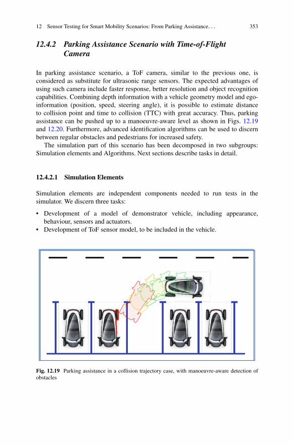
12 Sensor Testing for Smart Mobility Scenarios: From Parking Assistance. . . 353
12.4.2 Parking Assistance Scenario with Time-of-FlightCamera
In parking assistance scenario, a ToF camera, similar to the previous one, isconsidered as substitute for ultrasonic range sensors. The expected advantages ofusing such camera include faster response, better resolution and object recognitioncapabilities. Combining depth information with a vehicle geometry model and ego-information (position, speed, steering angle), it is possible to estimate distanceto collision point and time to collision (TTC) with great accuracy. Thus, parkingassistance can be pushed up to a manoeuvre-aware level as shown in Figs. 12.19and 12.20. Furthermore, advanced identification algorithms can be used to discernbetween regular obstacles and pedestrians for increased safety.
The simulation part of this scenario has been decomposed in two subgroups:Simulation elements and Algorithms. Next sections describe tasks in detail.
12.4.2.1 Simulation Elements
Simulation elements are independent components needed to run tests in thesimulator. We discern three tasks:
• Development of a model of demonstrator vehicle, including appearance,behaviour, sensors and actuators.
• Development of ToF sensor model, to be included in the vehicle.
Fig. 12.19 Parking assistance in a collision trajectory case, with manoeuvre-aware detection ofobstacles
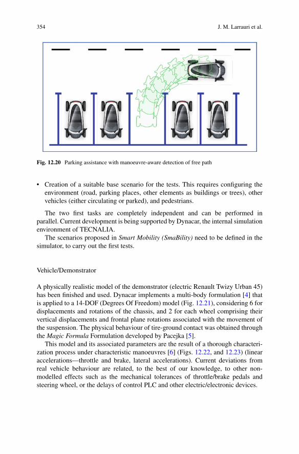
354 J. M. Larrauri et al.
Fig. 12.20 Parking assistance with manoeuvre-aware detection of free path
• Creation of a suitable base scenario for the tests. This requires configuring theenvironment (road, parking places, other elements as buildings or trees), othervehicles (either circulating or parked), and pedestrians.
The two first tasks are completely independent and can be performed inparallel. Current development is being supported by Dynacar, the internal simulationenvironment of TECNALIA.
The scenarios proposed in Smart Mobility (SmaBility) need to be defined in thesimulator, to carry out the first tests.
Vehicle/Demonstrator
A physically realistic model of the demonstrator (electric Renault Twizy Urban 45)has been finished and used. Dynacar implements a multi-body formulation [4] thatis applied to a 14-DOF (Degrees Of Freedom) model (Fig. 12.21), considering 6 fordisplacements and rotations of the chassis, and 2 for each wheel comprising theirvertical displacements and frontal plane rotations associated with the movement ofthe suspension. The physical behaviour of tire-ground contact was obtained throughthe Magic Formula Formulation developed by Pacejka [5].
This model and its associated parameters are the result of a thorough characteri-zation process under characteristic manoeuvres [6] (Figs. 12.22, and 12.23) (linearaccelerations—throttle and brake, lateral accelerations). Current deviations fromreal vehicle behaviour are related, to the best of our knowledge, to other non-modelled effects such as the mechanical tolerances of throttle/brake pedals andsteering wheel, or the delays of control PLC and other electric/electronic devices.
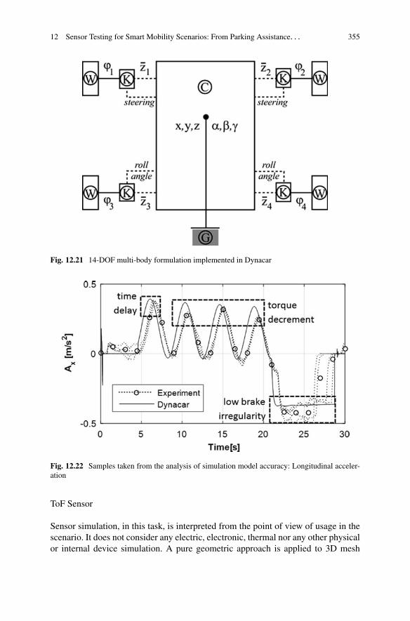
12 Sensor Testing for Smart Mobility Scenarios: From Parking Assistance. . . 355
Fig. 12.21 14-DOF multi-body formulation implemented in Dynacar
Fig. 12.22 Samples taken from the analysis of simulation model accuracy: Longitudinal acceler-ation
ToF Sensor
Sensor simulation, in this task, is interpreted from the point of view of usage in thescenario. It does not consider any electric, electronic, thermal nor any other physicalor internal device simulation. A pure geometric approach is applied to 3D mesh
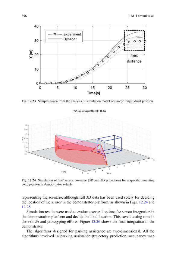
356 J. M. Larrauri et al.
Fig. 12.23 Samples taken from the analysis of simulation model accuracy: longitudinal position
Fig. 12.24 Simulation of ToF sensor coverage (3D and 2D projection) for a specific mountingconfiguration in demonstrator vehicle
representing the scenario, although full 3D data has been used solely for decidingthe location of the sensor in the demonstrator platform, as shown in Figs. 12.24 and12.25.
Simulation results were used to evaluate several options for sensor integration inthe demonstration platform and decide the final location. This saved testing time inthe vehicle and prototyping efforts. Figure 12.26 shows the final integration in thedemonstrator.
The algorithms designed for parking assistance are two-dimensional. All thealgorithms involved in parking assistance (trajectory prediction, occupancy map
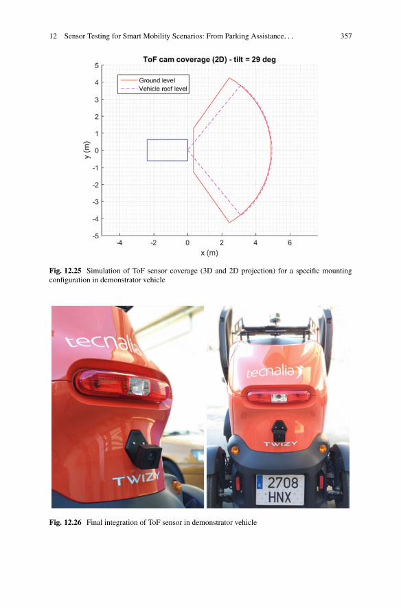
12 Sensor Testing for Smart Mobility Scenarios: From Parking Assistance. . . 357
Fig. 12.25 Simulation of ToF sensor coverage (3D and 2D projection) for a specific mountingconfiguration in demonstrator vehicle
Fig. 12.26 Final integration of ToF sensor in demonstrator vehicle
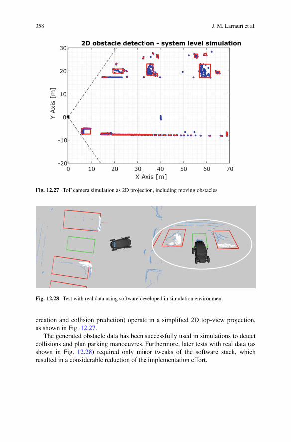
358 J. M. Larrauri et al.
Fig. 12.27 ToF camera simulation as 2D projection, including moving obstacles
Fig. 12.28 Test with real data using software developed in simulation environment
creation and collision prediction) operate in a simplified 2D top-view projection,as shown in Fig. 12.27.
The generated obstacle data has been successfully used in simulations to detectcollisions and plan parking manoeuvres. Furthermore, later tests with real data (asshown in Fig. 12.28) required only minor tweaks of the software stack, whichresulted in a considerable reduction of the implementation effort.

12 Sensor Testing for Smart Mobility Scenarios: From Parking Assistance. . . 359
Scenarios Configuration
A first test with the real sensor revealed several limiting factors that need to beconsidered in the design of the system. A preliminary set of scenarios was defined,covering combinations of four different variables:
• Parking type: parallel, perpendicular• External lighting conditions: high (outdoors, sunny), medium (outdoors,
cloudy/dusk/dawn), low (indoors or outdoors by night)• Optical characteristics of external materials: vehicles paint colour, shiny surfaces,
etc.• Moving obstacles: present, not present
Two of those factors (lighting conditions and optical characteristics of externalmaterials) have been translated into a simpler threshold for detection range: far (5 m)and close (2 m).
Moving obstacles (pedestrians) have been successfully added to the simulatedscenarios. Due to technical limitations, these elements are not visible in thegraphical interface of the simulation environment. However, they are simulated atsensor system and taken into account into the collisions detection algorithms.
The final set of simulation scenarios is composed by a total of eight samples,according to the table below (Table 12.4).
The particularities of the ToF sensor and its dependency of external materialsrequired a modelling detail that surpasses the capabilities of the selected simulationtools. This, the presented set of scenarios is intended to assist the integration ofassisted parking system components, rather than the implementation of the low-level algorithms for processing ToF camera data (Figs. 12.29 and 12.30).
12.4.2.2 Algorithms
The designed parking solution involves the development of four algorithmicmodules.
• Vehicle egomotion estimation• Vehicle trajectory prediction• ToF camera obstacle detection + identification• Time-to-collision reasoning
Vehicle Egomotion Estimation
Sensor acquisition and data fusion for estimation of vehicle position, speed, anglesand other egomotion variables. It is based in a standard implementation of theCartographer algorithm based on other vehicle sensors: GPS, IMU and Lidar.
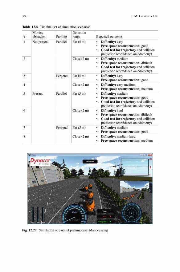
360 J. M. Larrauri et al.
Table 12.4 The final set of simulation scenarios
#Movingobstacles Parking
Detectionrange Expected outcome
1 Not present Parallel Far (5 m) • Difficulty: easy• Free-space reconstruction: good• Good test for trajectory and collision
prediction (confidence on odometry)2 Close (2 m) • Difficulty: medium
• Free-space reconstruction: difficult• Good test for trajectory and collision
prediction (confidence on odometry)3 Perpend Far (5 m) • Difficulty: easy
• Free-space reconstruction: good4 Close (2 m) • Difficulty: easy-medium
• Free-space reconstruction: medium5 Present Parallel Far (5 m) • Difficulty: medium
• Free-space reconstruction: good• Good test for trajectory and collision
prediction (confidence on odometry)6 Close (2 m) • Difficulty: hard
• Free-space reconstruction: difficult• Good test for trajectory and collision
prediction (confidence on odometry)7 Perpend Far (5 m) • Difficulty: medium
• Free-space reconstruction: good8 Close (2 m) • Difficulty: medium-hard
• Free-space reconstruction: medium
Fig. 12.29 Simulation of parallel parking case. Manoeuvring
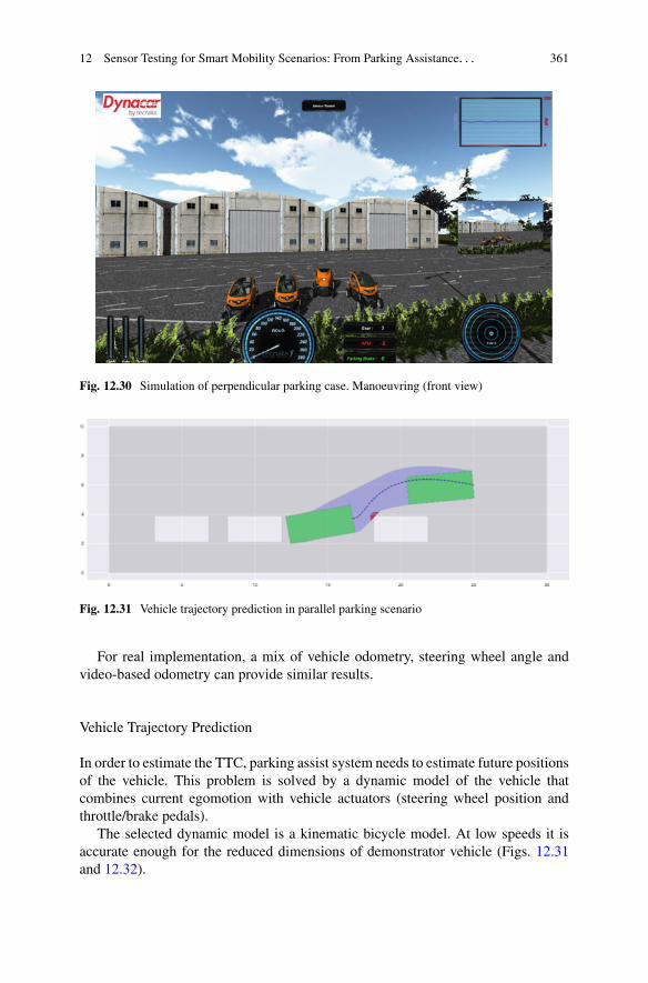
12 Sensor Testing for Smart Mobility Scenarios: From Parking Assistance. . . 361
Fig. 12.30 Simulation of perpendicular parking case. Manoeuvring (front view)
Fig. 12.31 Vehicle trajectory prediction in parallel parking scenario
For real implementation, a mix of vehicle odometry, steering wheel angle andvideo-based odometry can provide similar results.
Vehicle Trajectory Prediction
In order to estimate the TTC, parking assist system needs to estimate future positionsof the vehicle. This problem is solved by a dynamic model of the vehicle thatcombines current egomotion with vehicle actuators (steering wheel position andthrottle/brake pedals).
The selected dynamic model is a kinematic bicycle model. At low speeds it isaccurate enough for the reduced dimensions of demonstrator vehicle (Figs. 12.31and 12.32).
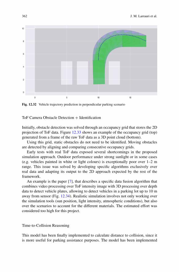
362 J. M. Larrauri et al.
Fig. 12.32 Vehicle trajectory prediction in perpendicular parking scenario
ToF Camera Obstacle Detection + Identification
Initially, obstacle detection was solved through an occupancy grid that stores the 2Dprojection of ToF data. Figure 12.33 shows an example of the occupancy grid (top)generated from a frame of the raw ToF data as a 3D point cloud (bottom).
Using this grid, static obstacles do not need to be identified. Moving obstaclesare detected by aligning and comparing consecutive occupancy grids.
Early tests with real ToF data exposed several shortcomings in the proposedsimulation approach. Outdoor performance under strong sunlight or in some cases(e.g. vehicles painted in white or light colours) is exceptionally poor over 1–2 mrange. This issue was solved by developing specific algorithms exclusively overreal data and adapting its output to the 2D approach expected by the rest of theframework.
An example is the paper [7], that describes a specific data fusion algorithm thatcombines video processing over ToF intensity image with 3D processing over depthdata to detect vehicle plates, allowing to detect vehicles in a parking lot up to 10 maway from sensor (Fig. 12.34). Realistic simulation involves not only working overthe simulation tools (sun position, light intensity, atmospheric conditions), but alsoover the scenarios to account for the different materials. The estimated effort wasconsidered too high for this project.
Time-to-Collision Reasoning
This model has been finally implemented to calculate distance to collision, since itis more useful for parking assistance purposes. The model has been implemented
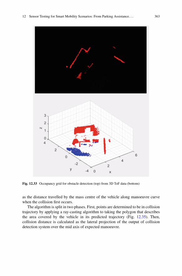
12 Sensor Testing for Smart Mobility Scenarios: From Parking Assistance. . . 363
Fig. 12.33 Occupancy grid for obstacle detection (top) from 3D ToF data (bottom)
as the distance travelled by the mass centre of the vehicle along manoeuvre curvewhen the collision first occurs.
The algorithm is split in two phases. First, points are determined to be in collisiontrajectory by applying a ray-casting algorithm to taking the polygon that describesthe area covered by the vehicle in its predicted trajectory (Fig. 12.35). Then,collision distance is calculated as the lateral projection of the output of collisiondetection system over the mid axis of expected manoeuvre.
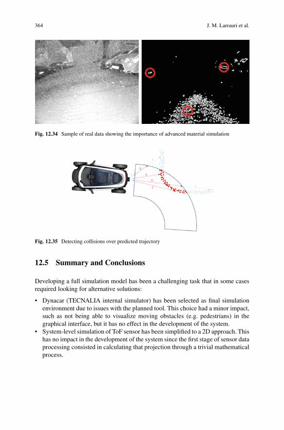
364 J. M. Larrauri et al.
Fig. 12.34 Sample of real data showing the importance of advanced material simulation
Fig. 12.35 Detecting collisions over predicted trajectory
12.5 Summary and Conclusions
Developing a full simulation model has been a challenging task that in some casesrequired looking for alternative solutions:
• Dynacar (TECNALIA internal simulator) has been selected as final simulationenvironment due to issues with the planned tool. This choice had a minor impact,such as not being able to visualize moving obstacles (e.g. pedestrians) in thegraphical interface, but it has no effect in the development of the system.
• System-level simulation of ToF sensor has been simplified to a 2D approach. Thishas no impact in the development of the system since the first stage of sensor dataprocessing consisted in calculating that projection through a trivial mathematicalprocess.
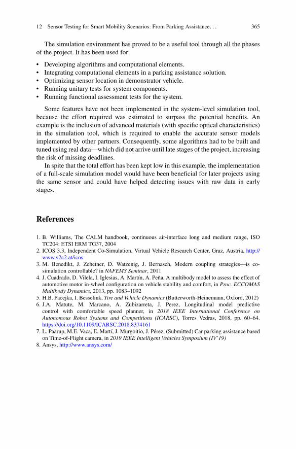
12 Sensor Testing for Smart Mobility Scenarios: From Parking Assistance. . . 365
The simulation environment has proved to be a useful tool through all the phasesof the project. It has been used for:
• Developing algorithms and computational elements.• Integrating computational elements in a parking assistance solution.• Optimizing sensor location in demonstrator vehicle.• Running unitary tests for system components.• Running functional assessment tests for the system.
Some features have not been implemented in the system-level simulation tool,because the effort required was estimated to surpass the potential benefits. Anexample is the inclusion of advanced materials (with specific optical characteristics)in the simulation tool, which is required to enable the accurate sensor modelsimplemented by other partners. Consequently, some algorithms had to be built andtuned using real data—which did not arrive until late stages of the project, increasingthe risk of missing deadlines.
In spite that the total effort has been kept low in this example, the implementationof a full-scale simulation model would have been beneficial for later projects usingthe same sensor and could have helped detecting issues with raw data in earlystages.
References
1. B. Williams, The CALM handbook, continuous air-interface long and medium range, ISOTC204: ETSI ERM TG37, 2004
2. ICOS 3.3, Independent Co-Simulation, Virtual Vehicle Research Center, Graz, Austria, http://www.v2c2.at/icos
3. M. Benedikt, J. Zehetner, D. Watzenig, J. Bernasch, Modern coupling strategies—is co-simulation controllable? in NAFEMS Seminar, 2011
4. J. Cuadrado, D. Vilela, I. Iglesias, A. Martín, A. Peña, A multibody model to assess the effect ofautomotive motor in-wheel configuration on vehicle stability and comfort, in Proc. ECCOMASMultibody Dynamics, 2013, pp. 1083–1092
5. H.B. Pacejka, I. Besselink, Tire and Vehicle Dynamics (Butterworth-Heinemann, Oxford, 2012)6. J.A. Matute, M. Marcano, A. Zubizarreta, J. Perez, Longitudinal model predictive
control with comfortable speed planner, in 2018 IEEE International Conference onAutonomous Robot Systems and Competitions (ICARSC), Torres Vedras, 2018, pp. 60–64.https://doi.org/10.1109/ICARSC.2018.8374161
7. L. Paarup, M.E. Vaca, E. Martí, J. Murgoitio, J. Pérez, (Submitted) Car parking assistance basedon Time-of-Flight camera, in 2019 IEEE Intelligent Vehicles Symposium (IV’19)
8. Ansys, http://www.ansys.com/
Chapter 13Health Monitoring for LightingApplications
W. D. van Driel, L. M. Middelburg, B. El Mansouri, and B. J. C. Jacobs
13.1 Introduction
The history of reliability as we know it now goes back to the 1950s, whenelectronics played a major role for the first time [1, 2]. Now, 70 decades later, theelectronic industry is facing a continuous increase of early and wear-out failureswith accompanying consequences. Figure 13.1 depicts the struggle for the differenthigh-tech industries, ranging from harsh environment suitability to long lifetimeand warranty coverage. Nowadays, products with high failure rates are logged onthe web leading to bad reputation for a company. In many ways, reliability ispart of everyday life and part of consumer expectations. The word reliability isextensively used by the general public and the technical community, as illustrated bythe following: there are over 3000 published books whose title or keywords containthe word reliability; the web of science lists some 10,000 technical papers with“reliability” as a keyword (since 1973); and the popular search engine Google listsover 12 million occurrences of “reliability” on the world wide web.
Solid state lighting applications are now at the doorstep of massive market entry[3, 4]. The penetration will grow most rapidly in the street and roadway and generalservice submarkets in terms of the percentage of total lumen-hour sales [5–7].Scenarios estimate the expected future adoption of LEDs based on historical data
W. D. van Driel (�)Delft University of Technology, EEMCS Faculty, Delft, The Netherlands
Signify, HTC48, Eindhoven, The Netherlandse-mail: [email protected]
L. M. Middelburg · B. El MansouriDelft University of Technology, EEMCS Faculty, Delft, The Netherlands
B. J. C. JacobsSignify, HTC48, Eindhoven, The Netherlands
© Springer Nature Switzerland AG 2020W. D. van Driel et al. (eds.), Sensor Systems Simulations,https://doi.org/10.1007/978-3-030-16577-2_13
367
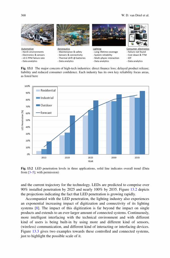
368 W. D. van Driel et al.
Fig. 13.1 The major concern of high-tech industries: direct finance loss; delayed product release;liability and reduced consumer confidence. Each industry has its own key reliability focus areas,as listed here
Fig. 13.2 LED penetration levels in three applications, solid line indicates overall trend (Datafrom [3–5]; with permission)
and the current trajectory for the technology. LEDs are predicted to comprise over90% installed penetration by 2025 and nearly 100% by 2035. Figure 13.2 depictsthe projections indicating the fact that LED penetration is growing rapidly.
Accompanied with the LED penetration, the lighting industry also experiencesan exponential increasing impact of digitization and connectivity of its lightingsystems [8]. The impact of this digitization is far beyond the impact on singleproducts and extends to an ever-larger amount of connected systems. Continuously,more intelligent interfacing with the technical environment and with differentkind of users is being built-in by using more and different kind of sensors,(wireless) communication, and different kind of interacting or interfacing devices.Figure 13.3 gives two examples towards these controlled and connected systems,just to highlight the possible scale of it.
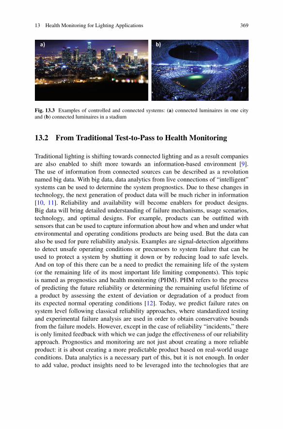
13 Health Monitoring for Lighting Applications 369
Fig. 13.3 Examples of controlled and connected systems: (a) connected luminaires in one cityand (b) connected luminaires in a stadium
13.2 From Traditional Test-to-Pass to Health Monitoring
Traditional lighting is shifting towards connected lighting and as a result companiesare also enabled to shift more towards an information-based environment [9].The use of information from connected sources can be described as a revolutionnamed big data. With big data, data analytics from live connections of “intelligent”systems can be used to determine the system prognostics. Due to these changes intechnology, the next generation of product data will be much richer in information[10, 11]. Reliability and availability will become enablers for product designs.Big data will bring detailed understanding of failure mechanisms, usage scenarios,technology, and optimal designs. For example, products can be outfitted withsensors that can be used to capture information about how and when and under whatenvironmental and operating conditions products are being used. But the data canalso be used for pure reliability analysis. Examples are signal-detection algorithmsto detect unsafe operating conditions or precursors to system failure that can beused to protect a system by shutting it down or by reducing load to safe levels.And on top of this there can be a need to predict the remaining life of the system(or the remaining life of its most important life limiting components). This topicis named as prognostics and health monitoring (PHM). PHM refers to the processof predicting the future reliability or determining the remaining useful lifetime ofa product by assessing the extent of deviation or degradation of a product fromits expected normal operating conditions [12]. Today, we predict failure rates onsystem level following classical reliability approaches, where standardized testingand experimental failure analysis are used in order to obtain conservative boundsfrom the failure models. However, except in the case of reliability “incidents,” thereis only limited feedback with which we can judge the effectiveness of our reliabilityapproach. Prognostics and monitoring are not just about creating a more reliableproduct: it is about creating a more predictable product based on real-world usageconditions. Data analytics is a necessary part of this, but it is not enough. In orderto add value, product insights need to be leveraged into the technologies that are
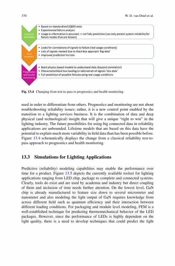
370 W. D. van Driel et al.
Fig. 13.4 Changing from test-to-pass to prognostics and health monitoring
used in order to differentiate from others. Prognostics and monitoring are not abouttroubleshooting reliability issues; rather, it is a new control point enabled by thetransition to a lighting services business. It is the combination of data and deepphysical (and technological) insight that will give a unique “right to win” in thelighting industry. The future possibilities for using big connected data in reliabilityapplications are unbounded. Lifetime models that are based on this data have thepotential to explain much more variability in field data than has been possible before.Figure 13.4 schematically displays the change from a classical reliability test-to-pass approach to prognostics and health monitoring.
13.3 Simulations for Lighting Applications
Predictive (reliability) modeling capabilities may enable the performance overtime for a product. Figure 13.5 depicts the currently available toolset for lightingapplications ranging from LED chip, package to complete and connected systems.Clearly, tools do exist and are used by academia and industry but direct couplingof them and inclusion of time needs further attention. On the lowest level, GaNchip is already manufactured to feature size down to several micrometer andnanometer and also modeling the light output of GaN requires knowledge fromacross different field such as quantum efficiency and their interaction betweendifferent loading conditions. For packaging and module level modeling, FEM is awell-established technique for predicting thermomechanical behavior of the LEDpackages. However, since the performance of LEDs is highly dependent on thelight quality, there is a need to develop techniques that could predict the light
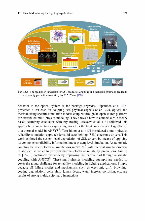
13 Health Monitoring for Lighting Applications 371
Fig. 13.5 The prediction landscape for SSL products. Coupling and inclusion of time is needed tocover reliability predictions (courtesy by C.A. Yuan, [19])
behavior in the optical system as the package degrades. Tapaninen et al. [13]presented a test case for coupling two physical aspects of an LED, optical andthermal, using specific simulation models coupled through an open source platformfor distributed multi-physics modeling. They showed how to connect a Mie theorybased scattering calculator with ray tracing. Alexeev et al. [14] followed thisapproach by connecting a ray-tracing model for the light conversion in LightTools
®
to a thermal model in ANSYS®
. Tarashioon et al. [15] introduced a multi-physicsreliability simulation approach for solid state lighting (SSL) electronic drivers. Thiswork explored the system-level degradation of SSL drivers by means of applyingits components reliability information into a system-level simulation. An automaticcoupling between electrical simulations in SPICE
®with thermal simulations was
established in order to perform thermal-electrical reliability predictions. Sun etal. [16–18] continued this work by improving the thermal part through automaticcoupling with ANSYS
®. These multi-physics modeling attempts are needed to
cover the grand challenge for reliability modeling in lighting applications. Simplybecause all failure modes and mechanisms such as electronic drift, browning,coating degradation, color shift, lumen decay, water ingress, corrosion, etc. areresults of strong multidisciplinary interactions.
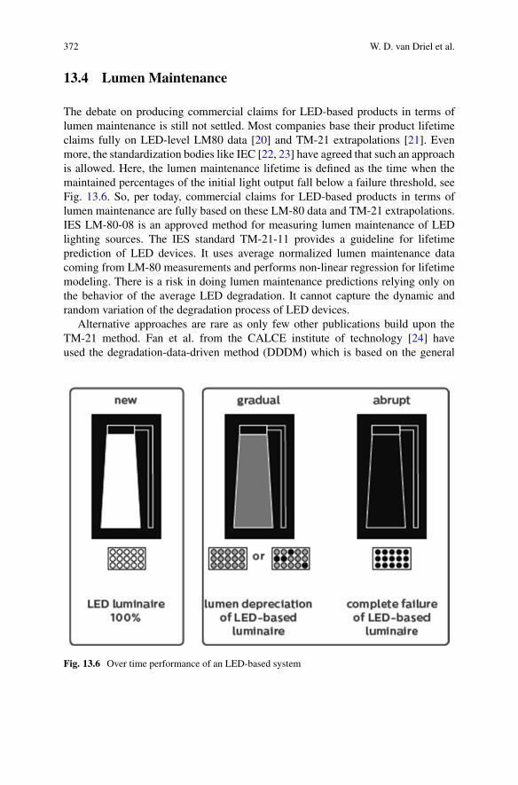
372 W. D. van Driel et al.
13.4 Lumen Maintenance
The debate on producing commercial claims for LED-based products in terms oflumen maintenance is still not settled. Most companies base their product lifetimeclaims fully on LED-level LM80 data [20] and TM-21 extrapolations [21]. Evenmore, the standardization bodies like IEC [22, 23] have agreed that such an approachis allowed. Here, the lumen maintenance lifetime is defined as the time when themaintained percentages of the initial light output fall below a failure threshold, seeFig. 13.6. So, per today, commercial claims for LED-based products in terms oflumen maintenance are fully based on these LM-80 data and TM-21 extrapolations.IES LM-80-08 is an approved method for measuring lumen maintenance of LEDlighting sources. The IES standard TM-21-11 provides a guideline for lifetimeprediction of LED devices. It uses average normalized lumen maintenance datacoming from LM-80 measurements and performs non-linear regression for lifetimemodeling. There is a risk in doing lumen maintenance predictions relying only onthe behavior of the average LED degradation. It cannot capture the dynamic andrandom variation of the degradation process of LED devices.
Alternative approaches are rare as only few other publications build upon theTM-21 method. Fan et al. from the CALCE institute of technology [24] haveused the degradation-data-driven method (DDDM) which is based on the general
Fig. 13.6 Over time performance of an LED-based system
13 Health Monitoring for Lighting Applications 373
degradation path model. They use it to predict the reliability of HP LEDs throughanalyzing the lumen maintenance data collected from the IES LM-80-08 lumenmaintenance test standard. Their method can get much more reliability informationout of the data (e.g., mean time to failure, confidence interval, reliability function).In an accompanying paper, Fan et al. [25] describe a particle filter-based (PF-based)prognostic approach based on both Sequential Monte Carlo (SMC) and Bayesiantechniques. These techniques are used to predict the lumen maintenance life ofLED light sources. Also, here the alternative approach achieves better predictionperformance, with an error of less than 5% in predicting the long-term lumenmaintenance life of LED light sources. Lall et al. [26] follow up on this approach byusing Bayesian Probabilistic Models for the assessment of the onset of degradationin solid state luminaires. The failure threshold decay rate has been calculated usingan Arrhenius model, neglecting the effects of current density and humidity. Thestatistical approach is quite valid but also seen as complicated. Quan et al. [27]describe an in-situ method to monitor the lumen degradation of LED packages. Theyconclude that the luminous flux of the LEDs shows a steady and slow depreciation,but no proper statistical analysis was performed on their measured data. Huanget al. [28–30] investigated the degradation mechanisms of mid-power white-lightLEDs. In their studies, a modified Wiener process was employed for the modelingof the LED devices’ degradation, following the earlier work of Tsai et al. [31]. Usingthis method, the dynamic, random variation, as well as the non-linear degradationbehaviors of the LED devices were described. They applied the Hallberg-Peck’smodel to describe the effects of temperature and humidity on LED degradation,thereby ignoring the crucial effects of the current density on this degradation.
Another alternative approach, used in this work, is to study the “degradation”data of each LED individually [32]. It means that for each individual LED a model asstated in Eq. (13.1) is fitted. Then, we can predict L70 values for each LED and turndegradation values into failure times. The mixed effects model is one of the mostpopular approaches in degradation analysis [33–35]. In order to describe the unit-to-unit variations of the test units, the unknown parameters of the mean degradationpath are described in terms of the mixed (or random) effects. Often the mixed effectsformulations do not take the time-dependent error structure into consideration.Therefore, the stochastic process formulation or Gauss-Markov method can be analternative approach to model the product’s degradation path. Dealing with thosemore complex models, to find the maximum likelihood estimates (MLEs) of theunknown parameters, the mixed effects model is computationally intensive. STATAor R can be used [36]. Here, the method by Meeker and Weaver [33] to analyze alarge set of LM80 data is chosen. In our approach, we have gathered LM80 setsof High Power (HP) LEDs, see table below. In total, we analyzed approximately27,000 data points (Table 13.1).
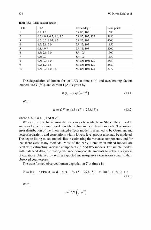
374 W. D. van Driel et al.
Table 13.1 LED dataset details
LED If [A] Tcase [degC] Read points
1 0.7; 1.0 55; 85; 105 16802 0.35; 0.5; 0.7; 1.0; 1.5 55; 85; 105; 125 38803 0.5; 0.7; 1.05; 1.2 55; 85; 105 42004 1.5; 2.1; 3.0 55; 85; 105 19505 0.35; 0.7 55; 85; 105 25006 1.5; 2.1; 3.0 85; 105 13007 0.5; 0.7 85; 105 15508 0.5; 0.7; 1.0; 55; 85; 105; 120 38509 0.7; 1.2; 1.5 55; 85; 105; 120 288010 0.5; 0.7; 1.0; 1.5 55; 85; 105; 125 2277
The degradation of lumen for an LED at time t [h] and accelerating factorstemperature T [◦C], and current I [A] is given by:
�(t) = exp(−αtβ
)(13.1)
With
α = CIn exp (B/ (T + 273.15)) (13.2)
where C > 0, n > 0, and B < 0We can use the linear mixed-effects models available in Stata. These models
are also known as multilevel models or hierarchical linear models. The overallerror distribution of the linear mixed-effects model is assumed to be Gaussian, andheteroskedasticity and correlations within lowest-level groups also may be modeled.The key to fitting mixed models lies in estimating the variance components, and forthat there exist many methods. Most of the early literature in mixed models aredealt with estimating variance components in ANOVA models. For simple modelswith balanced data, estimating variance components amounts to solving a systemof equations obtained by setting expected mean-squares expressions equal to theirobserved counterparts.
The transformed observed lumen degradation Y at time t is:
Y = ln (− ln (�(t))) = β · ln(t) + B/ (T + 273.15) + n · ln(I ) + ln(C) + ε
(13.3)
With:
ε∼iidN(
0, σ 2)
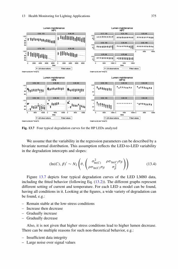
13 Health Monitoring for Lighting Applications 375
Fig. 13.7 Four typical degradation curves for the HP LEDs analyzed
We assume that the variability in the regression parameters can be described by abivariate normal distribution. This assumption reflects the LED-to-LED variabilityin the degradation intercepts and slopes:
(ln(C), β)′ ∼ N2
(θ,
(σ 2
ln(C) ρσ ln(C)σβ
ρσ ln(C)σβ σ 2β
))(13.4)
Figure 13.7 depicts four typical degradation curves of the LED LM80 data,including the fitted behavior (following Eq. (13.2)). The different graphs representdifferent setting of current and temperature. For each LED a model can be found,having all conditions in it. Looking at the figures, a wide variety of degradation canbe found, e.g.:
– Remain stable at the low-stress conditions– Increase then decrease– Gradually increase– Gradually decrease
Also, it is not given that higher stress conditions lead to higher lumen decrease.There can be multiple reasons for such non-theoretical behavior, e.g.:
– Insufficient data integrity– Large noise over signal values
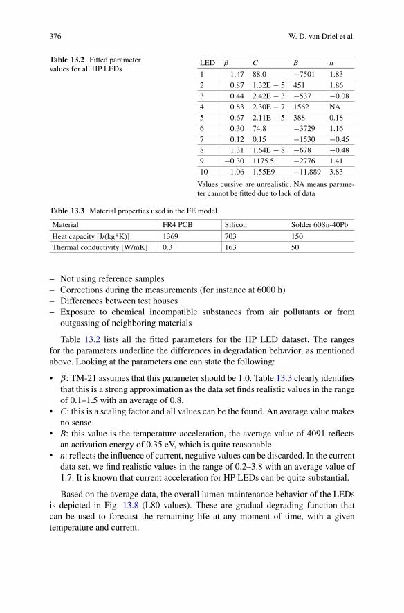
376 W. D. van Driel et al.
Table 13.2 Fitted parametervalues for all HP LEDs
LED β C B n
1 1.47 88.0 −7501 1.832 0.87 1.32E − 5 451 1.863 0.44 2.42E − 3 −537 −0.084 0.83 2.30E − 7 1562 NA5 0.67 2.11E − 5 388 0.186 0.30 74.8 −3729 1.167 0.12 0.15 −1530 −0.458 1.31 1.64E − 8 −678 −0.489 −0.30 1175.5 −2776 1.4110 1.06 1.55E9 −11,889 3.83
Values cursive are unrealistic. NA means parame-ter cannot be fitted due to lack of data
Table 13.3 Material properties used in the FE model
Material FR4 PCB Silicon Solder 60Sn-40Pb
Heat capacity [J/(kg*K)] 1369 703 150Thermal conductivity [W/mK] 0.3 163 50
– Not using reference samples– Corrections during the measurements (for instance at 6000 h)– Differences between test houses– Exposure to chemical incompatible substances from air pollutants or from
outgassing of neighboring materials
Table 13.2 lists all the fitted parameters for the HP LED dataset. The rangesfor the parameters underline the differences in degradation behavior, as mentionedabove. Looking at the parameters one can state the following:
• β: TM-21 assumes that this parameter should be 1.0. Table 13.3 clearly identifiesthat this is a strong approximation as the data set finds realistic values in the rangeof 0.1–1.5 with an average of 0.8.
• C: this is a scaling factor and all values can be the found. An average value makesno sense.
• B: this value is the temperature acceleration, the average value of 4091 reflectsan activation energy of 0.35 eV, which is quite reasonable.
• n: reflects the influence of current, negative values can be discarded. In the currentdata set, we find realistic values in the range of 0.2–3.8 with an average value of1.7. It is known that current acceleration for HP LEDs can be quite substantial.
Based on the average data, the overall lumen maintenance behavior of the LEDsis depicted in Fig. 13.8 (L80 values). These are gradual degrading function thatcan be used to forecast the remaining life at any moment of time, with a giventemperature and current.
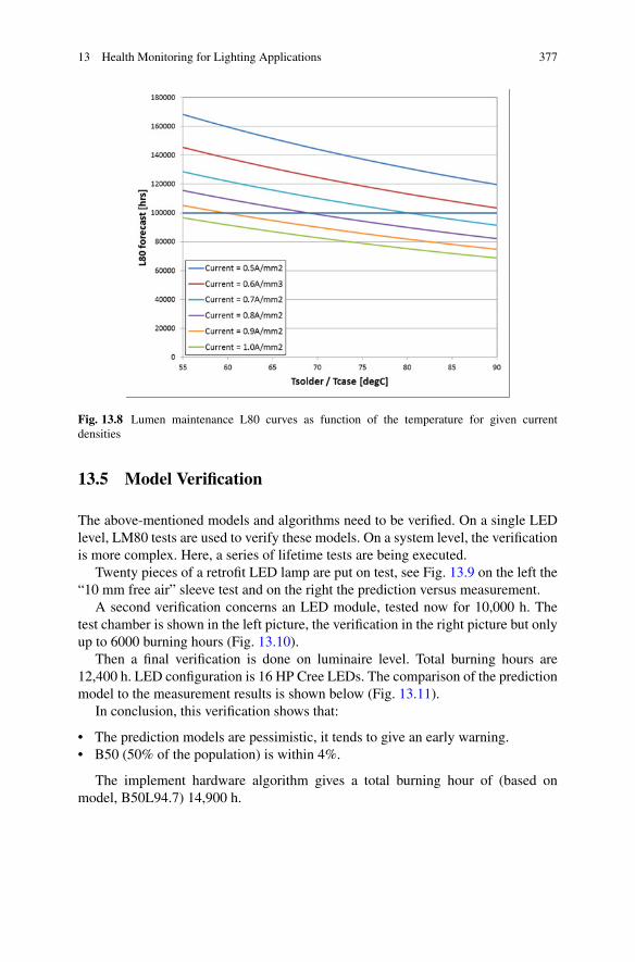
13 Health Monitoring for Lighting Applications 377
Fig. 13.8 Lumen maintenance L80 curves as function of the temperature for given currentdensities
13.5 Model Verification
The above-mentioned models and algorithms need to be verified. On a single LEDlevel, LM80 tests are used to verify these models. On a system level, the verificationis more complex. Here, a series of lifetime tests are being executed.
Twenty pieces of a retrofit LED lamp are put on test, see Fig. 13.9 on the left the“10 mm free air” sleeve test and on the right the prediction versus measurement.
A second verification concerns an LED module, tested now for 10,000 h. Thetest chamber is shown in the left picture, the verification in the right picture but onlyup to 6000 burning hours (Fig. 13.10).
Then a final verification is done on luminaire level. Total burning hours are12,400 h. LED configuration is 16 HP Cree LEDs. The comparison of the predictionmodel to the measurement results is shown below (Fig. 13.11).
In conclusion, this verification shows that:
• The prediction models are pessimistic, it tends to give an early warning.• B50 (50% of the population) is within 4%.
The implement hardware algorithm gives a total burning hour of (based onmodel, B50L94.7) 14,900 h.
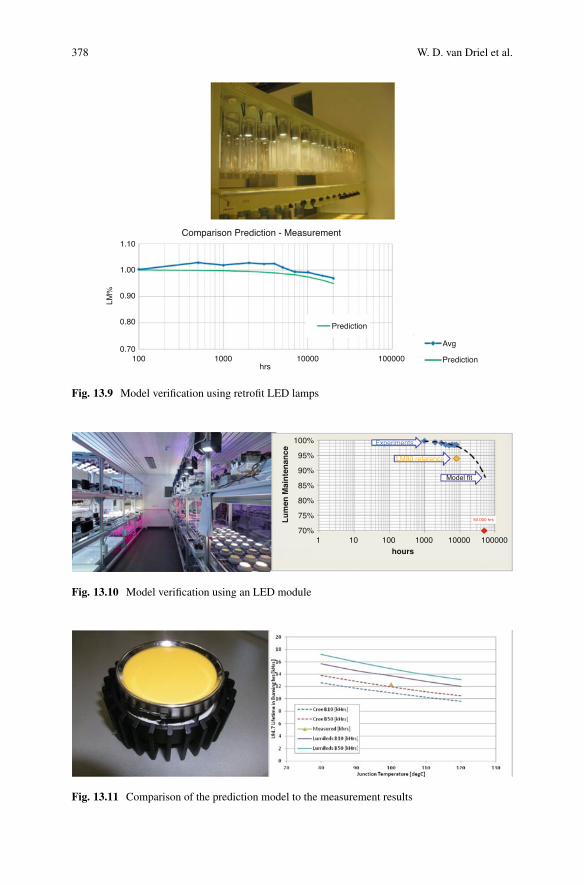
378 W. D. van Driel et al.
Comparison Prediction - Measurement1.10
1.00
LM%
0.90
0.80
0.70100 1000 10000
hrs
Prediction
Avg
Prediction100000
Fig. 13.9 Model verification using retrofit LED lamps
70%
Lu
men
Mai
nte
nan
ce
hours
75%
80%
85%
90%
95%
100%
1 10 100
Experiments
LM80 reference
Model fit
50.000 hrs
1000 10000 100000
Fig. 13.10 Model verification using an LED module
Fig. 13.11 Comparison of the prediction model to the measurement results
13 Health Monitoring for Lighting Applications 379
13.6 Uncertainty
Lighting systems are composed of many components (electronics, LEDs, customcomponents) assembled in a specified architecture and subjected to a certain userprofile. With the smart lighting demonstrator in mind, it is important to be able topredict the failure of the components with a certain acceptable level of uncertainty.Here the starting point are the failure time distributions of the separate components,and how these distributions depend on physical circumstances such as current,temperature, relative humidity, burning hours, and switches per day. The outputconsists of system failure percentiles over time for several failure criteria, lumenoutput over time, and Paretos describing what failures are most important. Thedistributions of the components are assumed to be true, and all output is conditionalon this assumption. For instance, the failure time of an electronics may be T~Weibull (α, β) where we take the given values of α, β for granted. However, inpractice, these may be estimated from a life time test with limited sample size,so that the sampling uncertainty is actually larger: if you would do the same testwith new systems, you would get different estimates for α, β. Note that in manycases there is an additional layer: α may depend on temperature and current viaadditional coefficients. The question that needs to be answered is: what are theimpacts of sampling uncertainty of component parameters on the spread of systemfailure probabilities?
Currently the system failure probability is considered at a given time, e.g., L70at 50 kh. These are in fact properties derived from probability distributions of thesystem. Here one is to add a statement to the value of B50L70 of how certain thatvalue is in view of the uncertainty of the components’ lifetime, in the form of saya 95% confidence interval that reflects that uncertainty. There are various randomquantities: for each component, and then usually a few physical failure mechanisms(e.g., for LEDs: solder failure, wirebond failure, speed of gradual decline of flux).If L70 is the random variable for the point in time at which the system crosses the70% of initial output level, we can view L70 as a function of those many randomvariables (per component, per failure type):
L70 = f(X1, . . . , Xp
)
X1 ∼ Distribution (α1, β1) , . . .(13.5)
The uncertainty on the many parameters of the input such as α1, β1 may bemodeled as (α1, β1) following some multivariate distribution, close to the samplingdistribution. In terms of Bayesian statistics, we specify some prior distributionon parameters such as (α1, β1). Between components and failure types these willbe independent. Under this prior distribution of the components, L70 has a priordistribution as well. Bayesian inference usually goes on by combining new datawith the prior beliefs, but that step is not going on in our case: just getting to knowthe prior distribution of quantities like L70 will be enough.
As demonstrated above, lumen maintenance follows an exponential decay withL70 as the point in time where lumen output drops below 70% of the initial value.L70 follows a lognormal distribution as L70(location, scale), with:

380 W. D. van Driel et al.
• location = log(C) – n * log(current) + B/Temperature• scale = sigma_lm from measurements
This results into the fact that the uncertainty depends on two parameters only,being location and scale. Typically, life time tests vary current and temperature andare used to estimate the regression coefficients.
The covariance between sigma and (C, n, B) will be zero, a property of the normaldistribution. So, it is a 3 × 3 covariance matrix.
log (− log(L)) = β log(t) + B · 1
T+ n · log(I ) + log(C) + ε (13.6)
As fitted in statistical software Stata [36]:
log (− log(L)) = βk log(t) + Bk · 1
T+ nk · log(I ) + ck + ε (13.7)
where (c, β) follows a bivariate normal distribution per LED and k is type. Let the
mean be (ck, βk) and write(ck, βk
)= (ck, βk) + (
εc, εβ
). Then the model is
log (− log(L)) = (βk + εβ
)log(t) + Bk · 1
T+ nk · log(I ) + ck + ε + εc (13.8)
Taking L = 0.7 and solve for t where ε = 0, first set d = log (− log (0.7)) =− 1.03:
d − Bk · 1
T− nk · log(I ) − ck − εc = (
βk + εβ
)log(t) (13.9)
The stochastics will be complex, assuming random components being zero, itresults:
location = log(L70) = 1βk
(d − Bk · 1
T− nk · log(I ) − ck
)
= log(
exp(
d−ck
βk
))−(
nk
βk
)· log(I ) +
(−Bk
βk
)· 1
T
= log (Clm) − nlm · log(I ) + Blm · 1T
(13.10)
The variance-covariance equals 1n
· V with n = nr of LEDs and V as follows:
symmetric avgV[3,3]
_nl_1 _nl_2 _nl_3
_nl_1 92.889581_nl_2 −13.417044 5.8164606_nl_3 −29731.637 2119.4056 11051779
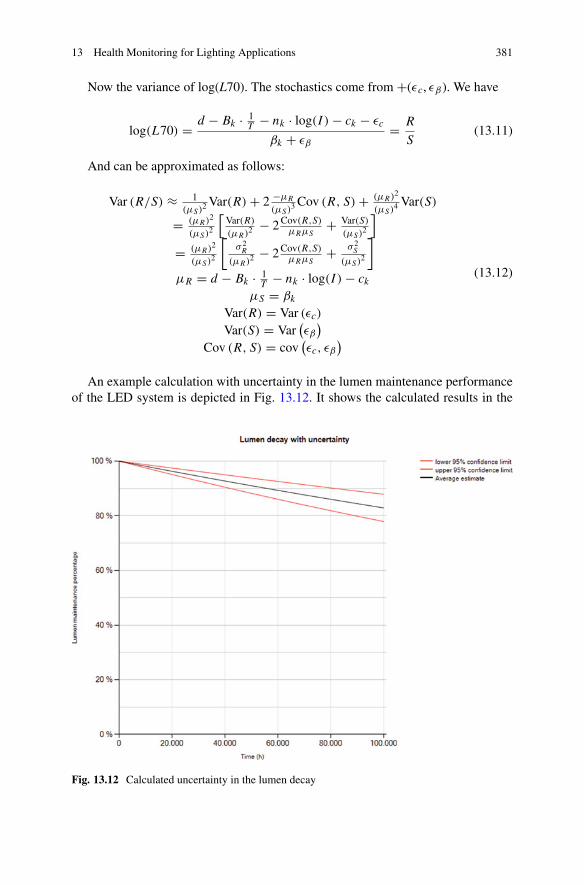
13 Health Monitoring for Lighting Applications 381
Now the variance of log(L70). The stochastics come from +(εc, εβ ). We have
log(L70) = d − Bk · 1T
− nk · log(I ) − ck − εc
βk + εβ
= R
S(13.11)
And can be approximated as follows:
Var (R/S) ≈ 1(μS)2 Var(R) + 2 −μR
(μS)3 Cov (R, S) + (μR)2
(μS)4 Var(S)
= (μR)2
(μS)2
[Var(R)
(μR)2 − 2 Cov(R,S)μRμS
+ Var(S)
(μS)2
]
= (μR)2
(μS)2
[σ 2
R
(μR)2 − 2 Cov(R,S)μRμS
+ σ 2S
(μS)2
]
μR = d − Bk · 1T
− nk · log(I ) − ck
μS = βk
Var(R) = Var (εc)
Var(S) = Var(εβ
)
Cov (R, S) = cov(εc, εβ
)
(13.12)
An example calculation with uncertainty in the lumen maintenance performanceof the LED system is depicted in Fig. 13.12. It shows the calculated results in the
Fig. 13.12 Calculated uncertainty in the lumen decay
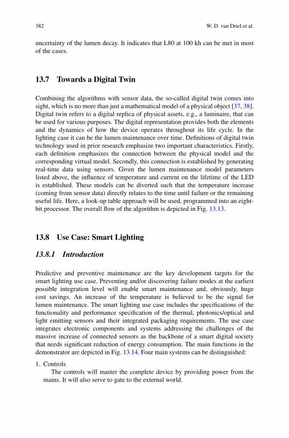
382 W. D. van Driel et al.
uncertainty of the lumen decay. It indicates that L80 at 100 kh can be met in mostof the cases.
13.7 Towards a Digital Twin
Combining the algorithms with sensor data, the so-called digital twin comes intosight, which is no more than just a mathematical model of a physical object [37, 38].Digital twin refers to a digital replica of physical assets, e.g., a luminaire, that canbe used for various purposes. The digital representation provides both the elementsand the dynamics of how the device operates throughout its life cycle. In thelighting case it can be the lumen maintenance over time. Definitions of digital twintechnology used in prior research emphasize two important characteristics. Firstly,each definition emphasizes the connection between the physical model and thecorresponding virtual model. Secondly, this connection is established by generatingreal-time data using sensors. Given the lumen maintenance model parameterslisted above, the influence of temperature and current on the lifetime of the LEDis established. These models can be diverted such that the temperature increase(coming from sensor data) directly relates to the time until failure or the remaininguseful life. Here, a look-up table approach will be used, programmed into an eight-bit processor. The overall flow of the algorithm is depicted in Fig. 13.13.
13.8 Use Case: Smart Lighting
13.8.1 Introduction
Predictive and preventive maintenance are the key development targets for thesmart lighting use case. Preventing and/or discovering failure modes at the earliestpossible integration level will enable smart maintenance and, obviously, hugecost savings. An increase of the temperature is believed to be the signal forlumen maintenance. The smart lighting use case includes the specifications of thefunctionality and performance specification of the thermal, photonics/optical andlight emitting sensors and their integrated packaging requirements. The use caseintegrates electronic components and systems addressing the challenges of themassive increase of connected sensors as the backbone of a smart digital societythat needs significant reduction of energy consumption. The main functions in thedemonstrator are depicted in Fig. 13.14. Four main systems can be distinguished:
1. ControlsThe controls will master the complete device by providing power from the
mains. It will also serve to gate to the external world.
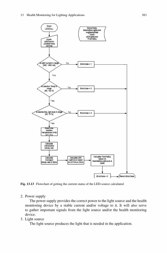
13 Health Monitoring for Lighting Applications 383
Fig. 13.13 Flowchart of getting the current status of the LED-source calculated
2. Power supplyThe power supply provides the correct power to the light source and the health
monitoring device by a stable current and/or voltage to it. It will also serveto gather important signals from the light source and/or the health monitoringdevice.
3. Light sourceThe light source produces the light that is needed in the application.
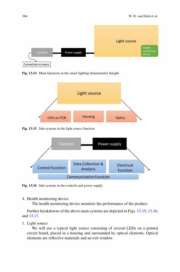
384 W. D. van Driel et al.
Fig. 13.14 Main functions in the smart lighting demonstrator Smight
Fig. 13.15 Sub-systems in the light source function
Fig. 13.16 Sub-systems in the controls and power supply
4. Health monitoring deviceThe health monitoring device monitors the performance of the product.
Further breakdowns of the above main systems are depicted in Figs. 13.15, 13.16,and 13.17.
1. Light sourceWe will use a typical light source consisting of several LEDs on a printed
circuit board, placed in a housing and surrounded by optical elements. Opticalelements are reflective materials and an exit window.
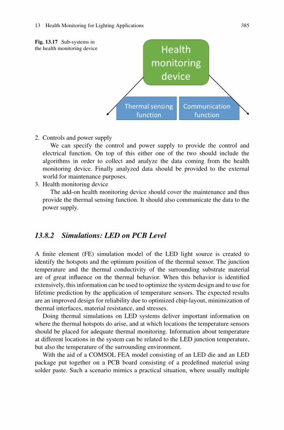
13 Health Monitoring for Lighting Applications 385
Fig. 13.17 Sub-systems inthe health monitoring device
2. Controls and power supplyWe can specify the control and power supply to provide the control and
electrical function. On top of this either one of the two should include thealgorithms in order to collect and analyze the data coming from the healthmonitoring device. Finally analyzed data should be provided to the externalworld for maintenance purposes.
3. Health monitoring deviceThe add-on health monitoring device should cover the maintenance and thus
provide the thermal sensing function. It should also communicate the data to thepower supply.
13.8.2 Simulations: LED on PCB Level
A finite element (FE) simulation model of the LED light source is created toidentify the hotspots and the optimum position of the thermal sensor. The junctiontemperature and the thermal conductivity of the surrounding substrate materialare of great influence on the thermal behavior. When this behavior is identifiedextensively, this information can be used to optimize the system design and to use forlifetime prediction by the application of temperature sensors. The expected resultsare an improved design for reliability due to optimized chip-layout, minimization ofthermal interfaces, material resistance, and stresses.
Doing thermal simulations on LED systems deliver important information onwhere the thermal hotspots do arise, and at which locations the temperature sensorsshould be placed for adequate thermal monitoring. Information about temperatureat different locations in the system can be related to the LED junction temperature,but also the temperature of the surrounding environment.
With the aid of a COMSOL FEA model consisting of an LED die and an LEDpackage put together on a PCB board consisting of a predefined material usingsolder paste. Such a scenario mimics a practical situation, where usually multiple
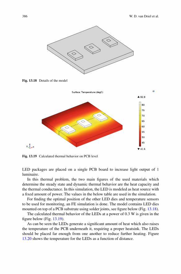
386 W. D. van Driel et al.
Fig. 13.18 Details of the model
Fig. 13.19 Calculated thermal behavior on PCB level
LED packages are placed on a single PCB board to increase light output of 1luminaire.
In this thermal problem, the two main figures of the used materials whichdetermine the steady state and dynamic thermal behavior are the heat capacity andthe thermal conductance. In this simulation, the LED is modeled as heat source witha fixed amount of power. The values in the below table are used in the simulation.
For finding the optimal position of the other LED dies and temperature sensorsto be used for monitoring, an FE simulation is done. The model contains LED diesmounted on top of a PCB substrate using solder joints, see figure below (Fig. 13.18).
The calculated thermal behavior of the LEDs at a power of 0.3 W is given in thefigure below (Fig. 13.19).
As can be seen the LEDs generate a significant amount of heat which also raisesthe temperature of the PCB underneath it, requiring a proper heatsink. The LEDsshould be placed far enough from one another to reduce further heating. Figure13.20 shows the temperature for the LEDs as a function of distance.
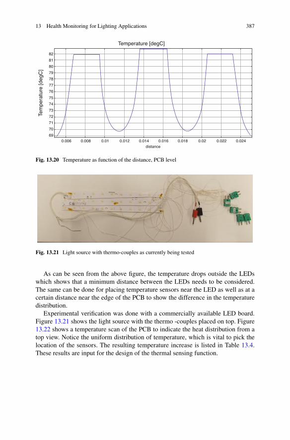
13 Health Monitoring for Lighting Applications 387
Temperature [degC]Te
mpe
ratu
re [d
egC
]
82
81
80
79
78
77
76
75
74
73
72
71
70
690.006 0.008 0.01 0.012 0.014
distance0.016 0.018 0.02 0.022 0.024
Fig. 13.20 Temperature as function of the distance, PCB level
Fig. 13.21 Light source with thermo-couples as currently being tested
As can be seen from the above figure, the temperature drops outside the LEDswhich shows that a minimum distance between the LEDs needs to be considered.The same can be done for placing temperature sensors near the LED as well as at acertain distance near the edge of the PCB to show the difference in the temperaturedistribution.
Experimental verification was done with a commercially available LED board.Figure 13.21 shows the light source with the thermo -couples placed on top. Figure13.22 shows a temperature scan of the PCB to indicate the heat distribution from atop view. Notice the uniform distribution of temperature, which is vital to pick thelocation of the sensors. The resulting temperature increase is listed in Table 13.4.These results are input for the design of the thermal sensing function.
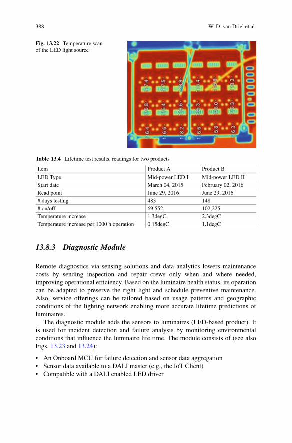
388 W. D. van Driel et al.
Fig. 13.22 Temperature scanof the LED light source
Table 13.4 Lifetime test results, readings for two products
Item Product A Product B
LED Type Mid-power LED I Mid-power LED IIStart date March 04, 2015 February 02, 2016Read point June 29, 2016 June 29, 2016# days testing 483 148# on/off 69,552 102,225Temperature increase 1.3degC 2.3degCTemperature increase per 1000 h operation 0.15degC 1.1degC
13.8.3 Diagnostic Module
Remote diagnostics via sensing solutions and data analytics lowers maintenancecosts by sending inspection and repair crews only when and where needed,improving operational efficiency. Based on the luminaire health status, its operationcan be adapted to preserve the right light and schedule preventive maintenance.Also, service offerings can be tailored based on usage patterns and geographicconditions of the lighting network enabling more accurate lifetime predictions ofluminaires.
The diagnostic module adds the sensors to luminaires (LED-based product). Itis used for incident detection and failure analysis by monitoring environmentalconditions that influence the luminaire life time. The module consists of (see alsoFigs. 13.23 and 13.24):
• An Onboard MCU for failure detection and sensor data aggregation• Sensor data available to a DALI master (e.g., the IoT Client)• Compatible with a DALI enabled LED driver
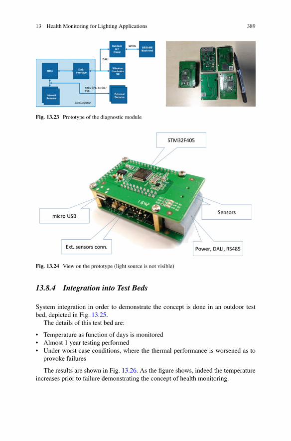
13 Health Monitoring for Lighting Applications 389
MCU
InternalSensors
DALIInterface
12C / SPI / 3x CS /3V3
ExternalSensors
XitaniumLuminaire
SR
OutdoorIoT
Client
SESAMEBack-end
GPRS
DALI
LumiDiagMod
Fig. 13.23 Prototype of the diagnostic module
Fig. 13.24 View on the prototype (light source is not visible)
13.8.4 Integration into Test Beds
System integration in order to demonstrate the concept is done in an outdoor testbed, depicted in Fig. 13.25.
The details of this test bed are:
• Temperature as function of days is monitored• Almost 1 year testing performed• Under worst case conditions, where the thermal performance is worsened as to
provoke failures
The results are shown in Fig. 13.26. As the figure shows, indeed the temperatureincreases prior to failure demonstrating the concept of health monitoring.
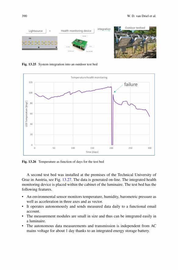
390 W. D. van Driel et al.
Fig. 13.25 System integration into an outdoor test bed
Fig. 13.26 Temperature as function of days for the test bed
A second test bed was installed at the premises of the Technical University ofGraz in Austria, see Fig. 13.27. The data is generated on-line. The integrated healthmonitoring device is placed within the cabinet of the luminaire. The test bed has thefollowing features.
• An environmental sensor monitors temperature, humidity, barometric pressure aswell as acceleration in three axes and as vector.
• It operates autonomously and sends measured data daily to a functional emailaccount.
• The measurement modules are small in size and thus can be integrated easily ina luminaire.
• The autonomous data measurements and transmission is independent from ACmains voltage for about 1 day thanks to an integrated energy storage battery.
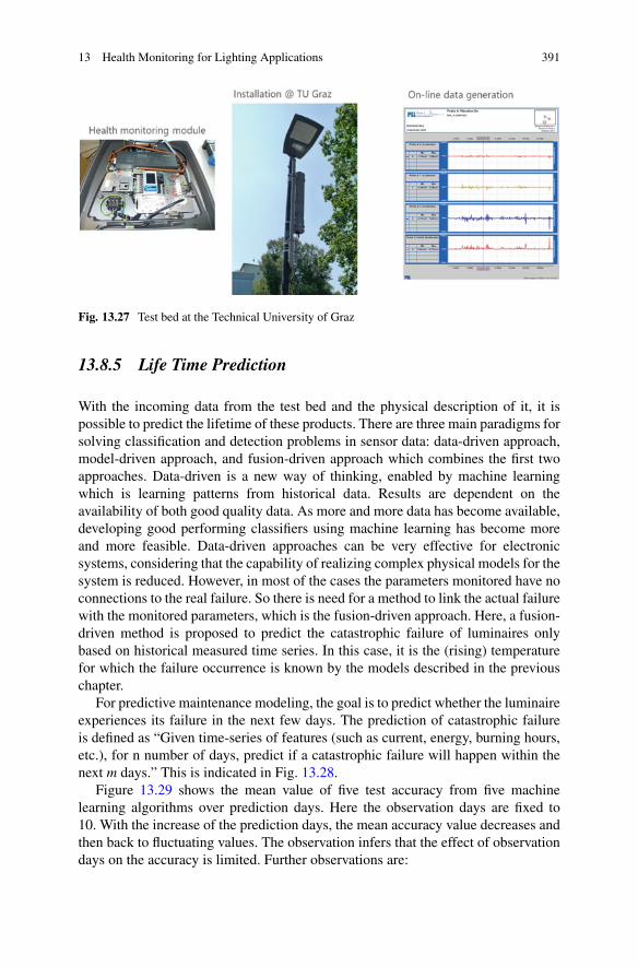
13 Health Monitoring for Lighting Applications 391
Fig. 13.27 Test bed at the Technical University of Graz
13.8.5 Life Time Prediction
With the incoming data from the test bed and the physical description of it, it ispossible to predict the lifetime of these products. There are three main paradigms forsolving classification and detection problems in sensor data: data-driven approach,model-driven approach, and fusion-driven approach which combines the first twoapproaches. Data-driven is a new way of thinking, enabled by machine learningwhich is learning patterns from historical data. Results are dependent on theavailability of both good quality data. As more and more data has become available,developing good performing classifiers using machine learning has become moreand more feasible. Data-driven approaches can be very effective for electronicsystems, considering that the capability of realizing complex physical models for thesystem is reduced. However, in most of the cases the parameters monitored have noconnections to the real failure. So there is need for a method to link the actual failurewith the monitored parameters, which is the fusion-driven approach. Here, a fusion-driven method is proposed to predict the catastrophic failure of luminaires onlybased on historical measured time series. In this case, it is the (rising) temperaturefor which the failure occurrence is known by the models described in the previouschapter.
For predictive maintenance modeling, the goal is to predict whether the luminaireexperiences its failure in the next few days. The prediction of catastrophic failureis defined as “Given time-series of features (such as current, energy, burning hours,etc.), for n number of days, predict if a catastrophic failure will happen within thenext m days.” This is indicated in Fig. 13.28.
Figure 13.29 shows the mean value of five test accuracy from five machinelearning algorithms over prediction days. Here the observation days are fixed to10. With the increase of the prediction days, the mean accuracy value decreases andthen back to fluctuating values. The observation infers that the effect of observationdays on the accuracy is limited. Further observations are:
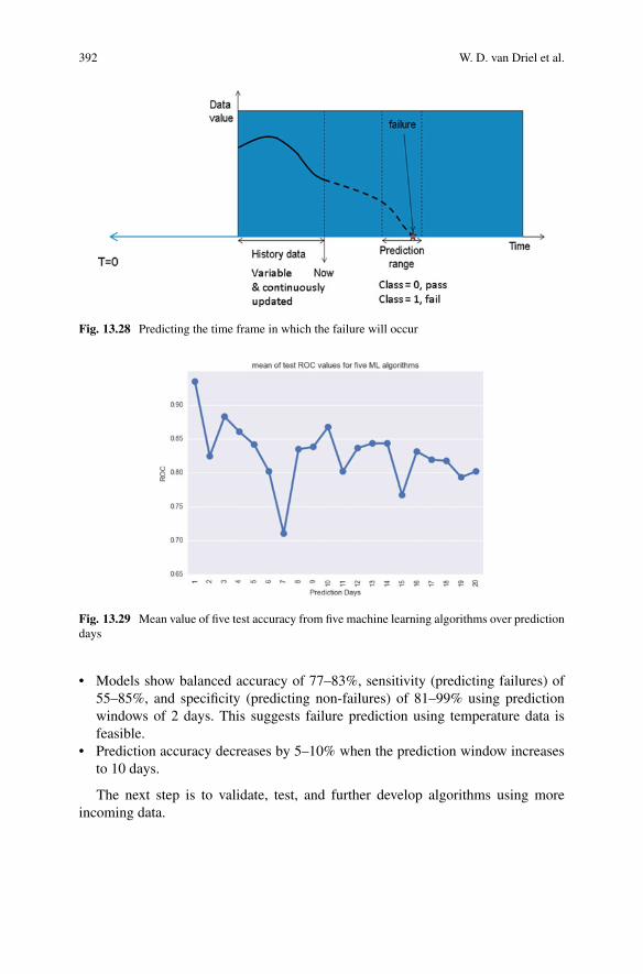
392 W. D. van Driel et al.
Fig. 13.28 Predicting the time frame in which the failure will occur
Fig. 13.29 Mean value of five test accuracy from five machine learning algorithms over predictiondays
• Models show balanced accuracy of 77–83%, sensitivity (predicting failures) of55–85%, and specificity (predicting non-failures) of 81–99% using predictionwindows of 2 days. This suggests failure prediction using temperature data isfeasible.
• Prediction accuracy decreases by 5–10% when the prediction window increasesto 10 days.
The next step is to validate, test, and further develop algorithms using moreincoming data.
13 Health Monitoring for Lighting Applications 393
13.8.6 Final Remarks
In the past 4 years, we have witnessed a substantial change in the lighting industry.Traditional companies have changed their strategy and upcoming competition haspushed down prices for LED-based products considerably. LED penetration levelsincreased so as the diversity of commercially available replacement products. Newprocesses and materials were introduced, and consequently new failure modesappeared. This trend will continue as the lighting industry is getting connectedand large amount of user data is being analyzed. New components are needed todeliver this functionality (sensors, actuator IoT modules) and, as such, the diversityfrom an architectural point of view will also increase. Gradually but slowly theterm reliability will be replaced by availability and “smart” maintenance willdistinguish good from bad products. In this chapter, we have presented a smartlighting use case in which the temperature rise served as indicating parameter forlumen maintenance. A fusion-driven approach combining sensor test data with aphysical system description was developed. In fact, these are our first steps towardsa digital twin for a connected luminaire.
Acknowledgments This work was supported by the European project “Iosense: Flexible FE/BESensor Pilot Line for the Internet of Everything.” This project has received funding from theElectronic Component Systems for European Leadership Joint Undertaking under grant agreementNo 692480. This Joint Undertaking receives support from the European Union’s Horizon 2020research and innovation programme and Germany, Netherlands, Spain, Austria, Belgium, Slovakia.
Thanks to the support from Harry Broers for providing the health monitoring device. Thanksto the support from Ulrich Boeke for designing and organizing the test bed in Graz and thanks tothe Technical University of Graz for hosting this test bed.
References
1. J. McLinn, A short history of reliability, J. Reliab. Inf. 30, 8–15 (2011)2. W. Denso, The history of reliability prediction. IEEE Trans. Reliab. 47(3-SP), 321–328 (1998)3. W. D. Van Driel, X. J. Fan (eds.), Solid State Lighting Reliability: Components to System
(Springer, New York, 2013)., ISBN 978-1-4614-3067-44. W. D. Van Driel, X. J. Fan, G. Q. Zhang (eds.), Solid State Lighting Reliability: Components
to System Part II (Springer, New York, 2017)., ISBN 978-3-319-58174-35. Navigant Consulting, Inc., Energy Savings Forecast of Solid-State Lighting in General
Illumination Applications, report prepared for the U.S. Department of Energy, August 20146. Navigant Consulting, Inc., Energy Savings Forecast of Solid-State Lighting in General
Illumination Applications, report prepared for the U.S. Department of Energy, September 20167. Estimated LED penetration of the global lighting market from 2010 to 2020, http://
www.statista.com/statistics/246030/estimated-led-penetration-of-the-global-lighting-market/(last visited on 8/25/2016)
8. D. Schenkelaars, W.D. van Driel, M. Klompenhouwer, I. Flinsenberg, R. Duijve, Towardsprognostics & health management in lighting applications, in European Conference of thePrognostics and Health Management Society 2016, open access journal, vol. 7, p. 7, 2016,http://www.phmsociety.org/node/2090/
394 W. D. van Driel et al.
9. S. Ismail, Exponential Organizations: Why New Organizations Are Ten Times Better, Faster,and Cheaper Than Yours (and What To Do About It) (Diversion Books, 2014)
10. W.Q. Meeker, Y. Hong, Reliability Meets Big Data: Opportunities and Challenges (2013).Statistics Preprints. Paper 82. http://lib.dr.iastate.edu/stat_las_preprints/82
11. W.Q. Meeker, L.A. Escobar, Statistical Methods for Reliability Data (Wiley, New York, 1998)12. M.G. Pecht, Prognostics and Health Management of Electronics (Wiley, Hoboken, 2008)13. O. Tapaninen, P. Myöhänen, A. Sitomaniemi, Optical and thermal simulation chain for
LED package, EuroSimE (http://www.eurosime.org/), 17th–20th of April 2015, Montpellier(France)
14. A. Alexeev, W. Cassarly, V.D. Hildenbrand, O. Tapaninen, A. Sitomaniemi, Simulating lightconversion in mid-power LEDs, EuroSimE (http://www.eurosime.org/), 17nd–20th of April2016, Montpellier (France)
15. S. Tarashioon, W.D. van Driel, G.Q. Zhang, Multi-physics reliability simulation for solid statelighting drivers. Microelectron. Reliab. (2014). https://doi.org/10.1016/j.microrel.2014.02.019
16. B. Sun, X.J. Fan, C. Qian, G.Q. Zhang, PoF-simulation-assisted reliability prediction forelectrolytic capacitor in LED drivers. IEEE Trans. Ind. Electron. 63(11), 6726–6735 (2016)
17. B. Sun, X.J. Fan, W.D. van Driel, H.Y. Ye, J.J. Fan, C. Qian, G.Q. Zhang, A novel lifetimeprediction for integrated LED lamps by electronic-thermal simulation. Reliab. Eng. Syst. Saf.163, 14–21 (2017)
18. B. Sun, X.J. Fan, H.Y Ye, G.Q. Zhang, A reliability prediction for integrated LED lampwith electrolytic capacitor-free driver, in IEEE Transactions on Components, Packaging andManufacturing Technology, 2017, p. 99
19. Communication with Dr. C.A. Yuan, owner of Ichijouriki LS R&D Co., Ltd, http://www.ichijouriki.com/, 26-09-2016
20. IES LM-80-08: Approved method for measuring maintenance of Led light sources21. IES TM-21-11: Projecting Long Term Lumen Maintenance of LED Light Sources22. IEC 62722-2-1, Luminaire performance—part 2-1: particular requirements for LED lumi-
naires, IEC standard, Edition 1.0 2014-1123. IEC 62717, LED modules for general lighting—performance requirements, IEC standard,
Edition 1.1 2015-0924. J. Fan, K.-C. Yung, M. Pecht, Lifetime estimation of high-power white LED using degradation-
data-driven method. IEEE Trans. Device Mater. Reliab. 12(2), 470–477 (2012)25. J. Fan, K.-C. Yung, M. Pecht, Predicting long-term lumen maintenance life of LED light
sources using a particle filter-based prognostic approach. Expert Syst. Appl. 42(5), 2411–2420(2015)
26. P. Lall, J. Wei, P. Sakalaukus, Bayesian models for life prediction and fault-mode classificationin solid state lamps, in 16th International Conference on Thermal, Mechanical and Multi-Physics Simulation and Experiments in Microelectronics and Microsystems, 2015
27. C. Quan, L. Xiaobing, C. Qi, W. Kai, L. Sheng, L. Jingyana, Research on lumen depreciationrelated to LED packages by in-situ measurement method. Microelectron. Reliab. 55, 2269–2275 (2015)
28. J.L. Huang, D.S. Golubovic, S. Koh, D.G. Yang, X.P. Li, X.J. Fan, G.Q. Zhang, Degradationmechanisms of mid-power white-light LEDs under high temperature-humidity conditions.IEEE Trans. Device Mater. Reliab. 15(2), 220–228 (2015)
29. J.L. Huang, D.S. Golubovic, S. Koh, D.G. Yang, X.P. Li, X.J. Fan, G.Q. Zhang, Degradationmodeling of mid-power white-light LEDs by using Wiener process. Opt. Express 23(15)(2015). https://doi.org/10.1364/OE.23.00A966
30. J.L. Huang, D.S. Golubovic, S. Koh, D.G. Yang, X.P. Li, X.J. Fan, G.Q. Zhang, Opticaldegradation mechanisms of mid-power white-light LEDs in LM-80-08 tests. Microelectron.Reliab. 55(12, Part B), 2654–2662 (2015)
31. T.-R. Tsai, C.-W. Lin, Y.-L. Sung, P.-T. Chou, C.-L. Chen, Y. Lio, Inference from lumendegradation data under Wiener diffusion process. IEEE Trans. Reliab. 61, 710–718 (2012)
32. W.D. van Driel, M. Schuld, B. Jacobs, F. Commissaris, J. van der Eyden, B. Hamon, Lumenmaintenance predictions for LED packages. Microelectron. Reliab. 62, 39–44 (2016)

13 Health Monitoring for Lighting Applications 395
33. W.Q. Meeker, L.A. Escobar, A review of accelerated test models. Stat. Sci. 21(4), 552–577(2006)
34. Y. Hong, W.Q. Meeker, Field-failure predictions based on failure-time datawith dynamic covariate information. Technometrics 55(2), 135–149 (2013).https://doi.org/10.1080/00401706.2013.765324
35. B.P. Weaver, W.Q. Meeker, Methods for planning repeated measures accelerated degradationtests. Stat. Qual. Prod. 30(6), 658–671 (2014)
36. STATA multilevel mixed effects reference manual, release 15, Stata Corp LLC, College Station,TX
37. Minds + Machines: Meet A Digital Twin, YouTube, GE Digital. Retrieved 26 July 201738. Introduction to Digital Twin: Simple, but detailed, YouTube, IBM Watson Internet of Things.
Retrieved 27 June 2017
Chapter 14Ultraviolet Sensing in WBG: SiC
B. El Mansouri, W. D. van Driel, and G. Q. Zhang
14.1 Introduction
The main application for the ultraviolet (UV) sensor is the detection of partialdischarge associated with power grid equipment, but not limited to this. TheUV electromagnetic radiation occupies the spectral range of 10–400 nm. TheUV radiation is used in many applications ranging from chemical processes suchas lithography to biology. The UV spectral range is typically divided into fourwavelength (λ) regions as illustrated in Fig. 14.1.
The photodetection is then also classified according to the UV range of interest[1–4]. The photodetectors are referred to as solar-visible for the spectral range aboveUVA [1]. Another special range is the deep UV (DUV) range of 220–280 nm [1, 3].Here the DUV radiation from the sun is mostly absorbed by the ozone layer leavinglonger wavelengths than 280 nm (UVC) to reach earth. This gives the opportunityto use photodetection in the lower wavelength region without being affected bythe sun, hence the classification as solar blind photodetection. As for wavelengthsshorter than 200 nm, these will be absorbed by the oxygen in the atmosphere. Thephotodiodes can further be classified depending on the used materials, structure ofthe sensor, insulation, filtering and so on.
Most common photodetectors are semiconductor based, i.e. photoconductors,photodiodes such as PN, pin and MS and MSM diodes, and phototransistors.
B. El Mansouri · G. Q. ZhangDelft University of Technology, EEMCS Faculty, Delft, The Netherlandse-mail: [email protected]; [email protected]
W. D. van Driel (�)Delft University of Technology, EEMCS Faculty, Delft, The Netherlands
Signify, HTC48, Eindhoven, The Netherlandse-mail: [email protected]; [email protected]
© Springer Nature Switzerland AG 2020W. D. van Driel et al. (eds.), Sensor Systems Simulations,https://doi.org/10.1007/978-3-030-16577-2_14
397
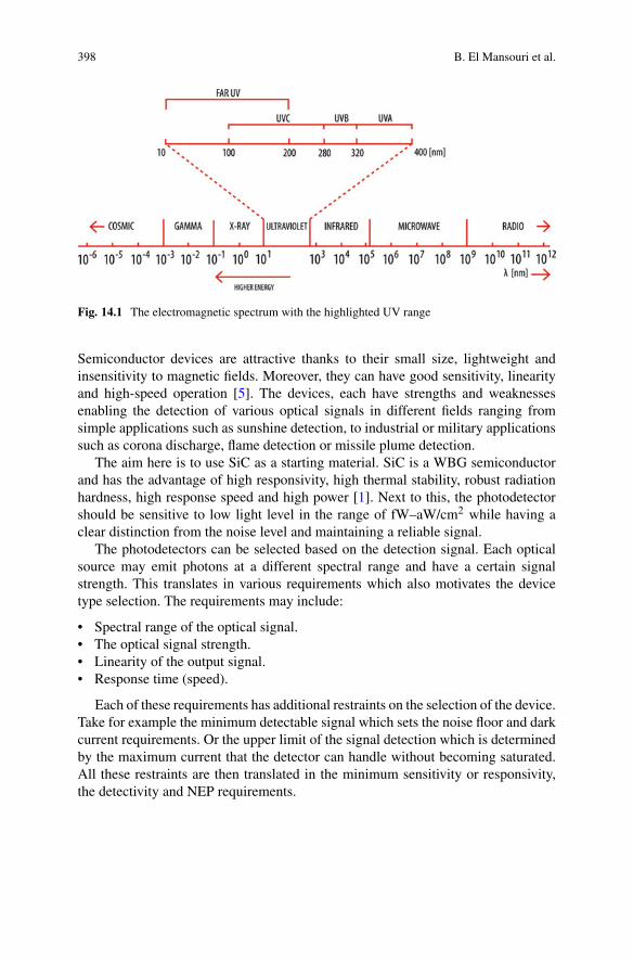
398 B. El Mansouri et al.
Fig. 14.1 The electromagnetic spectrum with the highlighted UV range
Semiconductor devices are attractive thanks to their small size, lightweight andinsensitivity to magnetic fields. Moreover, they can have good sensitivity, linearityand high-speed operation [5]. The devices, each have strengths and weaknessesenabling the detection of various optical signals in different fields ranging fromsimple applications such as sunshine detection, to industrial or military applicationssuch as corona discharge, flame detection or missile plume detection.
The aim here is to use SiC as a starting material. SiC is a WBG semiconductorand has the advantage of high responsivity, high thermal stability, robust radiationhardness, high response speed and high power [1]. Next to this, the photodetectorshould be sensitive to low light level in the range of fW–aW/cm2 while having aclear distinction from the noise level and maintaining a reliable signal.
The photodetectors can be selected based on the detection signal. Each opticalsource may emit photons at a different spectral range and have a certain signalstrength. This translates in various requirements which also motivates the devicetype selection. The requirements may include:
• Spectral range of the optical signal.• The optical signal strength.• Linearity of the output signal.• Response time (speed).
Each of these requirements has additional restraints on the selection of the device.Take for example the minimum detectable signal which sets the noise floor and darkcurrent requirements. Or the upper limit of the signal detection which is determinedby the maximum current that the detector can handle without becoming saturated.All these restraints are then translated in the minimum sensitivity or responsivity,the detectivity and NEP requirements.
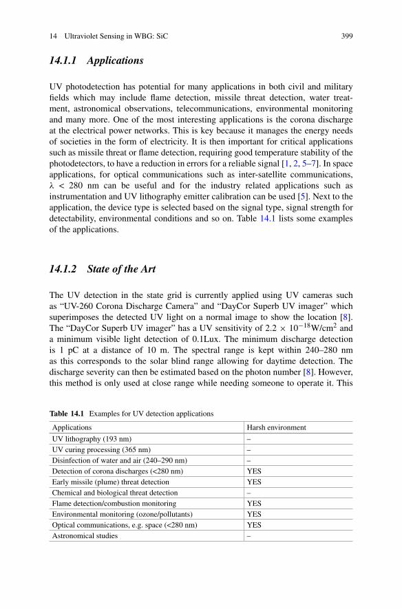
14 Ultraviolet Sensing in WBG: SiC 399
14.1.1 Applications
UV photodetection has potential for many applications in both civil and militaryfields which may include flame detection, missile threat detection, water treat-ment, astronomical observations, telecommunications, environmental monitoringand many more. One of the most interesting applications is the corona dischargeat the electrical power networks. This is key because it manages the energy needsof societies in the form of electricity. It is then important for critical applicationssuch as missile threat or flame detection, requiring good temperature stability of thephotodetectors, to have a reduction in errors for a reliable signal [1, 2, 5–7]. In spaceapplications, for optical communications such as inter-satellite communications,λ < 280 nm can be useful and for the industry related applications such asinstrumentation and UV lithography emitter calibration can be used [5]. Next to theapplication, the device type is selected based on the signal type, signal strength fordetectability, environmental conditions and so on. Table 14.1 lists some examplesof the applications.
14.1.2 State of the Art
The UV detection in the state grid is currently applied using UV cameras suchas “UV-260 Corona Discharge Camera” and “DayCor Superb UV imager” whichsuperimposes the detected UV light on a normal image to show the location [8].The “DayCor Superb UV imager” has a UV sensitivity of 2.2 × 10⁻¹⁸W/cm2 anda minimum visible light detection of 0.1Lux. The minimum discharge detectionis 1 pC at a distance of 10 m. The spectral range is kept within 240–280 nmas this corresponds to the solar blind range allowing for daytime detection. Thedischarge severity can then be estimated based on the photon number [8]. However,this method is only used at close range while needing someone to operate it. This
Table 14.1 Examples for UV detection applications
Applications Harsh environment
UV lithography (193 nm) –UV curing processing (365 nm) –Disinfection of water and air (240–290 nm) –Detection of corona discharges (<280 nm) YESEarly missile (plume) threat detection YESChemical and biological threat detection –Flame detection/combustion monitoring YESEnvironmental monitoring (ozone/pollutants) YESOptical communications, e.g. space (<280 nm) YESAstronomical studies –
400 B. El Mansouri et al.
shows that developing sensors that can be employed over the entire grid offer bettermonitoring of the power grid.
Next to the camera, an imaging system was also developed to detect ultravioletdetection [9, 10]. The imaging sensor is able not only to detect hydrogen flamesbut also corona discharge at a proximity. The UV light intensity detected for thelatter is 37 nW/cm2 with a 400 lux background light intensity. The imaging sensoris based on CMOS technology while the photodetection is obtained using an organicphotoconductive film (OPF). The film is not only sensitive in the UV range but alsoin the visible range and therefore a smart imaging scheme was used to detect boththe visible and UV radiation at the same time. This enables a normal image with animposed UV image.
14.2 Device Types
There are various technologies used for photodetection application ranging fromvacuum tube devices used as photomultipliers (PMTs) to semiconductor devicessuch as photoconductor, Schottky diodes and pn-junctions including their adap-tations [1, 5]. Here, two structure types are used, the MSM and device types.Therefore, the discussion in this chapter will limit itself to the discussion anddevelopment of these devices.
14.2.1 The Photoconductor
The photoconductor, also referred to as a photoresistor, is an ohmic photodetector.The device has a simple design comprised of a pair of ohmic electrodes with on thetop surface a highly doped semiconductor absorbing layer and an electrode on eachside, as shown in Fig. 14.2.
The MSM photoconductor allows for simple fabrication not only reducing costbut is an advantage as no additional epitaxial layer is needed and hard materials suchas SiC are less of an issue regarding implantation, diffusion and etching. Further thedevice can realize a large area of detection. The conductivity of the semiconductor
Metal Metal
Semiconductor
Fig. 14.2 Metal-semiconductor-metal photoconductor

14 Ultraviolet Sensing in WBG: SiC 401
is dependent on the amount of incident photons which in turn excite electrons to theconduction band enabling a higher conductivity of the material. When the electrodesare biased, the electrical field will drive the photogenerated e-h pairs to separateand move towards the electrodes resulting in a photocurrent in the external circuitproportional to the photon lux [1]. In the absence of incident photons, the darkcurrent of the device is given by
Id = V
Rd(14.1)
where Rd is the resistance of the material in the dark. Since the conductivity isdependent on the incident photons with sufficient energy, the resistance of thesemiconductor will drop resulting in a photocurrent given by
Ip = V
(1
Ri− 1
Rd
)(14.2)
where Ri is the resistance under illumination. Figure 14.3 illustrates the I-Vcharacteristics of the photoconductor in the dark and under illumination [2].
The full expression for the photocurrent in a photoconductive device is givenby [11]
Ip =(
Popt
hv
)qηG =
(Popt
hc
)λqηG (14.3)
with
G = μτV
s2(14.4)
Fig. 14.3 I-V characteristicsof a photoconductor
Dark
Illuminated
Ubias
Iphoto
I
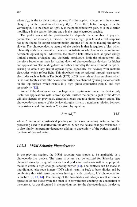
402 B. El Mansouri et al.
where Popt is the incident optical power, V is the applied voltage, q is the electroncharge, η is the quantum efficiency (QE), hv is the photon energy, λ is thewavelength, c is the speed of light, G is the photoconductive gain, μ is the electronmobility, τ is the carrier lifetime and s is the inter-electrodes spacing.
The performance of the photoconductor depends on a number of physicalparameters. For instance, a trade-off between a high gain G and a fast responsehas to be found for longer recombination lifetime of the holes making the deviceslower. The photoconductive nature of the device is that it requires a bias whichinherently adds dark current to the noise contributions which reduces the minimumdetectable optical signal. Moreover, the electric field effects such as space chargelimited current, avalanche and dielectric breakdown limit the photocurrent andtherefore become an issue for scaling down of photoconductor devices for higherend applications. The scaling down is further limited by the area required for opticalsensing to obtain any useful optical signal especially for devices with metallicelectrodes which reflect light. This drawback can be reduced through transparentelectrodes such as Indium Tin Oxide (ITO) or 2D materials such as graphene whichis the case for this work. The device can further be enhanced by using nanomaterialson the top surface which results in a high photo conductive gain G and highresponsivity [12].
Some of the drawbacks such as large area requirement render the device onlyuseful for applications with slower speeds. Further the output signal of the devicewill also depend on previously detected signals due to a photo memory effect. Thephotoconductive nature of the device also gives rise to a nonlinear relation betweenthe resistance and illumination Ei as given by equation
R = AE−αi (14.5)
where A and α are constants depending on the semiconducting material and theprocessing used to manufacture the device. Since the device changes resistance, itis also highly temperature dependent adding to uncertainty of the optical signal inthe form of thermal noise.
14.2.2 MSM Schottky Photodetector
In the previous section, the MSM structure was shown to be applicable as aphotoconductive device. The same structure can be utilized for Schottky typephotodetectors by using intrinsic or low doped semiconductors with an appropriatemetal to create a high enough Schottky barrier [13]. The contacts can be made asinterdigitated electrode fingers (IDT) which result in back-to-back diodes and bycombining this with semiconductors having a wide bandgap, UV photodetectionis enabled [2, 13, 14]. The biasing of the two diodes will always result in reverseoperation of one diode while the other is in forward bias enabling the conduction ofthe current. As was discussed in the previous text for the photoconductor, the device
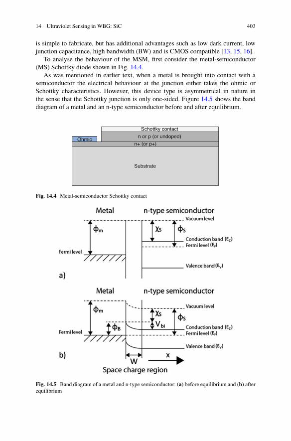
14 Ultraviolet Sensing in WBG: SiC 403
is simple to fabricate, but has additional advantages such as low dark current, lowjunction capacitance, high bandwidth (BW) and is CMOS compatible [13, 15, 16].
To analyse the behaviour of the MSM, first consider the metal-semiconductor(MS) Schottky diode shown in Fig. 14.4.
As was mentioned in earlier text, when a metal is brought into contact with asemiconductor the electrical behaviour at the junction either takes the ohmic orSchottky characteristics. However, this device type is asymmetrical in nature inthe sense that the Schottky junction is only one-sided. Figure 14.5 shows the banddiagram of a metal and an n-type semiconductor before and after equilibrium.
Schottky contact
Substrate
Ohmicn or p (or undoped)
n+ (or p+)
Fig. 14.4 Metal-semiconductor Schottky contact
Fig. 14.5 Band diagram of a metal and n-type semiconductor: (a) before equilibrium and (b) afterequilibrium

404 B. El Mansouri et al.
In the above figure, χ s is the semiconductor electron affinity, φs is the semi-conductor workfunction, φm is the metal workfunction, φB is the Schottky barrierheight, Vbi is the built-in voltage and W is the space charge region (SCR) widthalong the distance x. Figure 14.5a shows the Fermi levels of the metal and semi-conductor before equilibrium is reached. Upon contact between the two materials,the Fermi energy level becomes constant throughout the structure reaching anequilibrium. This is thanks to a flow of electrons from the semiconductor intothe lower energy states of the metal leaving positively charged ions behind, thuscreating a depletion region (SCR). It should be noted that Fig. 14.5b assumes themetal workfunction to be larger compared to that of the semiconductor else anohmic contact will be the result. For p-type semiconductors this is the opposite.Table 14.2 summarizes the requirements for Schottky and ohmic contacts for bothsemiconductor types. Table 14.3 lists the work functions of several metals and theresulting barrier height for 4H-SiC having an electron affinity of 3.3 eV.
As a result of the shown band bending, a potential barrier φB known as theSchottky barrier is seen by the electrons in the metal side trying to move to thesemiconductor. Ideally, the Schottky barrier height is given by
φB = φm − χs (14.6)
The equation shows the Schottky contact dependence on the semiconductorelectron affinity (χ s) and the metal workfunction (φm) · χ s is given by
χs = φs − (Ec − Ef) (14.7)
Table 14.2 Schottky contactworkfunctions requirement
Semiconductor Schottky (rectifying) Ohmic
n-type φm > φs φm < φs
p-type φm < φs φm > φs
Table 14.3 Relevant metals and their workfunctions
Metal Workfunction (φm) eV Barrier height 4H-SiC (φm) eV
Au 5.10 1.80Ag 4.26 0.96Al 4.28 0.98B 4.45 1.15Cr 4.50 1.20Cu 4.65 1.35Ni 5.15 1.85Pt 5.65 2.35W 4.55 1.25

14 Ultraviolet Sensing in WBG: SiC 405
On the other hand, after the band bending the electrons from the semiconductorside will also see a built-in potential barrier known as the built-in voltage Vbi givenby
Vbi = φm − φs = φB − (Ec − Ef) (14.8)
As discussed before, the semiconductor should be low doped to achieve Schottkybarrier behaviour. The reason behind this is the dependence of the built-in voltageon doping similar to the pn-junction. This dependence is shown below equations.
Ec − Ef = kBT
qln
(Nc
Nd
)(14.9)
Yielding
Vbi = φm − χs − kBT
qln
(Nc
Nd
)= φB − kBT
qln
(Nc
Nd
)(14.10)
where kB is the Boltzmann’s constant, T is the temperature and Nd is the donor con-centration. The built-in voltage is the barrier seen by electrons in the semiconductorwhich prevents further flow of electrons into the metal. Nc is the effective density ofstates in the conduction band and is given by
Nc = 4√
23√
πm∗kBT
h3 (14.11)
where m∗ is the effective electron mass and h is the Planck’s constant(h = 6.63 · 10−34 m2 · kg · s−1). Using the above equation for the built-in voltage, agraph can be constructed for the dependence on the doping concentration of n-type4H-SiC, see Fig. 14.6.
The above figure assumes Nickel is used as a Schottky metal contact at atemperature of 300 K. To calculate the effective density, the anisotropic nature of the4H-SiC needs to be considered since the effective mass varies for different crystalorientations.
When a Schottky contact is biased, either reverse or forward, the barrier heightwill change as shown in Fig. 14.7a, b.
The electrons in the semiconductor will easily diffuse across the SCR into metalfor a sufficiently reduced barrier height due to forward bias (Vbi − VF). On the otherhand, for Vbi + VR the barrier will be increased blocking the electrons. Furthermore,the above diagrams are very similar to those of a pn-junction resulting in similar I-V characteristics with exponential behaviour. However, the current mechanism inthe MS junction is due to the flow of majority carrier electrons as opposed to thepn-junction, allowing for high-speed operation. The high speed is also thanks tothe one-sided depletion region of the Schottky diode. Similar to a pn-junction the
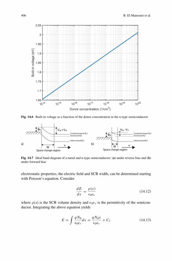
406 B. El Mansouri et al.
Fig. 14.6 Built-in voltage as a function of the donor concentration in the n-type semiconductor
Fig. 14.7 Ideal band diagram of a metal and n-type semiconductor: (a) under reverse bias and (b)under forward bias
electrostatic properties, the electric field and SCR width, can be determined startingwith Poisson’s equation. Consider
dE
dx= ρ(x)
ε0εr
(14.12)
where ρ(x) is the SCR volume density and ε0εr is the permittivity of the semicon-ductor. Integrating the above equation yields
E =∫
qNd
ε0εr
dx = qNdx
ε0εr
+ C1 (14.13)

14 Ultraviolet Sensing in WBG: SiC 407
To solve for the integration constant, assume electric field at the SCR edge of thesemiconductor to be zero.
C1 = qNdx
ε0εr
(14.14)
Assuming the SCR starts at x = 0 and extends to x = W, the electric field at anypoint y in the x-direction can be written as
E = −qNd (W − x)
ε0εr
(14.15)
The SCR width can be determined by assuming a highly doped p layer torepresent the metal in a p+n junction. The SCR in the n-type semiconductor undera reverse bias then becomes
W =√
2ε0εr (Vbi + VR)
qNd(14.16)
It should be noted that the photogenerated e-h pairs outside the SCR willrecombine before reaching the electrodes. Charge carriers generated in the SCRwill be collected at the electrodes before recombination takes place. Now that thesingle junction contact is introduced, this can be extended with a second contact.Consider Fig. 14.8a, b showing the MSM band diagram after equilibrium and theback-to-back diodes.
As can be seen from the above figure, the two contacts to the semiconductor aresymmetrical of nature. However, when a bias is applied to the device this symmetryis broken where one barrier height is increased, and the other is lowered. This resultsin an operation where one diode is always reverse biased and the other forwardbiased allowing the flow of charge carriers to form a current in an external circuit. Asa consequence, the MSM Schottky device will exhibit nonlinear I-V characteristics.This method allows for a low dark current, hence the minimum detectable signal
Fig. 14.8 (a) MSM band diagram after equilibrium and (b) MSM back-to-back diodes
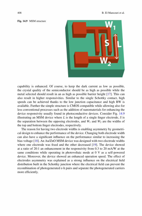
408 B. El Mansouri et al.
Fig. 14.9 MSM structure
capability is enhanced. Of course, to keep the dark current as low as possible,the crystal quality of the semiconductor should be as high as possible while themetal selected should result in an as high as possible barrier height [17]. This canalso result in higher responsivities. Similar to the single Schottky contact, highspeeds can be achieved thanks to the low junction capacitance and high BW isavailable. Further the simple structure is CMOS compatible while allowing also forless conventional processes such as the addition of nanomaterials for enhancing thedevice responsivity usually found in photoconductive devices. Consider Fig. 14.9illustrating an MSM device where L is the length of a single finger electrode, S isthe separation between the opposing electrodes, and W1 and W2 are the widths ofthe top and bottom finger electrodes, respectively.
The reason for having two electrode widths is enabling asymmetry by geometri-cal design to enhance the performance of the device. Changing both electrode widthcan also have a significant influence on the performance similar to increasing thebias voltage [18]. An Au/ZnO MSM device was designed with two electrode widthswhere one electrode was fixed and the other decreased [19]. The device showedat a ratio of 20:1 an enhancement in the responsivity from 0.3 to 20 mA/W at thesame conditions while operating in photovoltaic mode at 0 V as a self-powereddevice. Moreover, the device showed an enhanced operation speed. The effect ofelectrodes asymmetry was explained as a strong influence on the electrical fielddistribution built in the Schottky junction where the electrical field can prevent therecombination of photogenerated e-h pairs and separate the photogenerated carriersmore efficiently.

14 Ultraviolet Sensing in WBG: SiC 409
14.2.3 MS Schottky Contact Current Mechanism
The current mechanisms in Schottky contact devices is due to three main mech-anisms: thermionic emission (TE), thermionic field emission (TFE) and fieldemission (FE) [17]. Figure 14.10 illustrates these effects.
Thermionic emission describes the electron flow over the potential barrier whenthe charge carriers gain enough thermal energy while assuming the barrier heightto be larger than the thermal voltage (kBT/q). This is dominant in moderatelydoped semiconductors operating at room temperature and is used to describe theI-V characteristics of the MS Schottky contact.
The current density given by TE is according to Eq. (14.17).
J = Js
(exp
(qV
kBT
)− 1
)(14.17)
where V is the applied voltage. The saturation current Js is given by
Js = A∗∗T 2 exp
(−qφB
kBT
)(14.18)
where A∗∗ is the effective Richardson constant. This equation allows for thecalculation of the barrier height using the I-V characteristic of a MS Schottkydevice. Js is found experimentally.
Thermionic field emission results from high electric field application to thesemiconductor under temperatures relatively higher than room temperature. As aresult, the current density due to this mechanism will be higher as compared to TEand FE mechanisms.
Field emission, also known as quantum tunnelling, is due to the narrowing ofthe potential barrier as a result of high electric field giving the electrons a higherprobability of tunnelling through the barrier. This mechanism is more dominant
Fig. 14.10 Schottky contactcurrent mechanisms
410 B. El Mansouri et al.
for high doping concentrations in the semiconductor or at low temperatures. Thetunnelling current is given by
Jt = Jts exp
(−qφB
E00
)(14.19)
where Jts is the tunnelling saturation current and E00 is the characteristic tunnellingenergy related to the tunnelling effect transmission probability. E00 is given by
E00 = qh
4π
√Nd
εsm∗ (14.20)
This parameter helps predict which mechanism will be dominating depending onthree conditions given by the ratio E00/kBT as shown by
Condition 1 : E00
qkBT≤ 0.2 (14.21)
Condition 2 : 0.2 <E00
qkBT≤ 5 (14.22)
Condition 3 : E00
qkBT> 5 (14.23)
From these equations, it should be possible to calculate at room tem-perature and see that TE dominates at N ≤ 3 × 1017cm−3 and TFE at3 · 1017cm−3 ≤ N ≤ 2 · 1020cm−3. At higher doping levels, FE becomes dominant.Recombination in the SCR and recombination in neutral region under forwardbias also contribute to the current. In this work TE is considered since low dopedsemiconductors are used for the fabrication of the MSM Schottky devices. There areother effects in the device associated with the metal-semiconductor contact. Suchcan be the image-force, interface layers, traps and other defects, etc. Such effectsmay be discussed when relevant for the characterization of the device.
14.2.4 PN-Junction Photodiode
The pn-junction photodiode is one of the first junction semiconducting devicescreated. It is a simple structure consisting of a p-type layer on top of an n-typelayer or substrate. By bringing the two-layer types a potential barrier exists underequilibrium and no net current flow through the diode exists. Figure 14.11 shows anillustration of the device along with its electrical symbol.
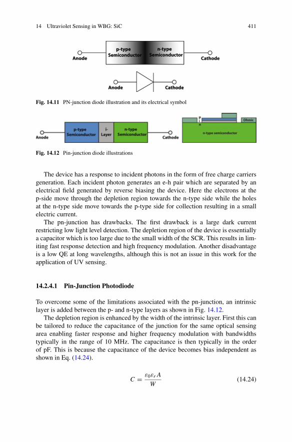
14 Ultraviolet Sensing in WBG: SiC 411
Fig. 14.11 PN-junction diode illustration and its electrical symbol
Fig. 14.12 Pin-junction diode illustrations
The device has a response to incident photons in the form of free charge carriersgeneration. Each incident photon generates an e-h pair which are separated by anelectrical field generated by reverse biasing the device. Here the electrons at thep-side move through the depletion region towards the n-type side while the holesat the n-type side move towards the p-type side for collection resulting in a smallelectric current.
The pn-junction has drawbacks. The first drawback is a large dark currentrestricting low light level detection. The depletion region of the device is essentiallya capacitor which is too large due to the small width of the SCR. This results in lim-iting fast response detection and high frequency modulation. Another disadvantageis a low QE at long wavelengths, although this is not an issue in this work for theapplication of UV sensing.
14.2.4.1 Pin-Junction Photodiode
To overcome some of the limitations associated with the pn-junction, an intrinsiclayer is added between the p- and n-type layers as shown in Fig. 14.12.
The depletion region is enhanced by the width of the intrinsic layer. First this canbe tailored to reduce the capacitance of the junction for the same optical sensingarea enabling faster response and higher frequency modulation with bandwidthstypically in the range of 10 MHz. The capacitance is then typically in the orderof pF. This is because the capacitance of the device becomes bias independent asshown in Eq. (14.24).
C = ε0εrA
W(14.24)
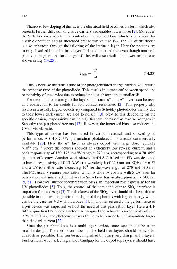
412 B. El Mansouri et al.
Thanks to low doping of the layer the electrical field becomes uniform which alsopresents further diffusion of charge carriers and enables lower noise [2]. Moreover,the SCR becomes nearly independent of the applied bias which is beneficial fora stable operation and an increased breakdown voltage Vbr. The QE of the deviceis also enhanced through the tailoring of the intrinsic layer. Here the photons aremostly absorbed in the intrinsic layer. It should be noted that even though more e-hpairs can be generated for a larger W, this will also result in a slower response asshown in Eq. (14.25).
Tdrift = W
Vd(14.25)
This is because the transit time of the photogenerated charge carriers will reducethe response time of the photodiode. This results in a trade-off between speed andresponsivity of the device due to reduced photon absorption at smaller W.
For the ohmic contacting to the layers additional n+ and p+ layers can be usedas a connection to the metals for low contact resistances [2]. This property alsoresults in a usually higher detectivity compared to Schottky photodiodes mainly dueto their lower dark current (related to noise) [13]. Next to this depending on thespecific design, responsivity can be significantly increased at reverse voltages inSchottky and p-n photodetectors [13]. However, the increased bias also reduces theUV-to-visible ratio.
This type of device has been used in various research and showed goodperformance. A 6H-SiC UV pin-junction photodetector is already commerciallyavailable [20]. Here the n+ layer is always doped with large dose typically>1019 cm−3 where the devices showed an extremely low reverse current, and apeak responsivity of 150–175 mA/W range at 270 nm, corresponding to a 70–85%quantum efficiency. Another work showed a 4H-SiC based pin PD was designedto have a responsivity of 0.13 A/W at a wavelength of 270 nm, an EQE of ∼61%and a UV-to-visible ratio exceeding 103 for the wavelength of 270 and 380 nm.The PDs usually require passivation which is done by coating with SiO2 layer forpassivation and antireflection where the SiO2 layer has an absorption at λ < 200 nm[5, 21]. However, surface recombination plays an important role especially for farUV photodiodes [5]. Thus, the control of the semiconductor to SiO2 interface isimportant for the design [5]. The thickness of the SiO2 layer should also be as thin aspossible to improve the penetration depth of the photons with higher energy whichcan be the case for VUV photodiodes [5]. In another research, the performance ofa p-n device was improved without the need of this passivation layer. Here a 4H-SiC pn-junction UV photodetector was designed and achieved a responsivity of 0.03A/W at 280 nm. The photocurrent was found to be four orders of magnitude largerthan the dark current [22].
Since the pin photodiode is a multi-layer device, some care should be takeninto the design. The absorption losses in the field-free layers should be avoidedas much as possible. This can be accomplished by using very thin p- and n-layers.Furthermore, when selecting a wide bandgap for the doped top layer, it should have
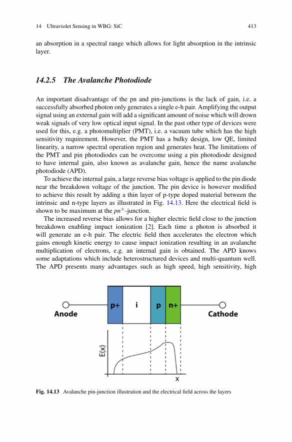
14 Ultraviolet Sensing in WBG: SiC 413
an absorption in a spectral range which allows for light absorption in the intrinsiclayer.
14.2.5 The Avalanche Photodiode
An important disadvantage of the pn and pin-junctions is the lack of gain, i.e. asuccessfully absorbed photon only generates a single e-h pair. Amplifying the outputsignal using an external gain will add a significant amount of noise which will drownweak signals of very low optical input signal. In the past other type of devices wereused for this, e.g. a photomultiplier (PMT), i.e. a vacuum tube which has the highsensitivity requirement. However, the PMT has a bulky design, low QE, limitedlinearity, a narrow spectral operation region and generates heat. The limitations ofthe PMT and pin photodiodes can be overcome using a pin photodiode designedto have internal gain, also known as avalanche gain, hence the name avalanchephotodiode (APD).
To achieve the internal gain, a large reverse bias voltage is applied to the pin diodenear the breakdown voltage of the junction. The pin device is however modifiedto achieve this result by adding a thin layer of p-type doped material between theintrinsic and n-type layers as illustrated in Fig. 14.13. Here the electrical field isshown to be maximum at the pn+-junction.
The increased reverse bias allows for a higher electric field close to the junctionbreakdown enabling impact ionization [2]. Each time a photon is absorbed itwill generate an e-h pair. The electric field then accelerates the electron whichgains enough kinetic energy to cause impact ionization resulting in an avalanchemultiplication of electrons, e.g. an internal gain is obtained. The APD knowssome adaptations which include heterostructured devices and multi-quantum well.The APD presents many advantages such as high speed, high sensitivity, high
Fig. 14.13 Avalanche pin-junction illustration and the electrical field across the layers
414 B. El Mansouri et al.
responsivity, high internal gain and even low noise. For example, 4H-SiC APDsexhibit low noise thanks to the large ionization coefficient ratio of ∼10 betweenholes and electrons [5, 23]. The APD can also be based on other types of junctionssuch as the MS junction [2] but is by far based on the pin-junction. The latter showstrade-offs between the maximum achievable responsivity, speed and operatingvoltage [2, 23].
Of course, the APD also has disadvantages. The multiplication effect not onlyresults in a higher photocurrent, but also in a higher dark current and lower noiseperformance while also adding noise from the multiplication process itself. Thebandwidth of the device becomes smaller while the response time increases due tothe avalanche build-up time and holes transit time through the absorption region.
The devices can be improved using various techniques. A pin-junction photode-tector was fabricated and showed a dark current density of 63 nA/cm2 at 90 pA, a QEof 40% and a gain of 103. The same device was optimized using a recessed-windowstructure and by improving the antireflection (AR) coating layer [24]. The workshowed a responsivity of 136 mA/W at 262 nm, with an EQE of 60%, avalanchegains of over 106, an excess noise factor characterized by k value of ∼0.1, and aspatially uniform response [25]. The pin-junction device performance can be furtherimproved by using a separate absorption and multiplication (SAM) structure [23].A SAM-APD has separate high-field multiplication and absorption regions and byoptimizing the thicknesses and doping concentrations of these layers, some of theissues associated with the pin-structure APD can be solved [23]. For instance, theSAM-APD structure injects only a single type of carrier into the multiplicationregion which reduces the multiplication noise that arises from the stochastic natureof the multiplication process [23]. The fabricated device achieved an optical gainhigher than 1.8 · 104 at 90% of the breakdown voltage of about 55 V. At 42 Vreverse bias and 270 nm wavelength, the peak responsivity increased to 0.203 A/W,corresponding to a maximum EQE of ∼93% [23].
14.3 Operation Modes
14.3.1 Photovoltaic Mode
The photodetectors can be operated in either the photovoltaic (PV) or photocon-ductive (PC) modes. Devices based on Schottky barrier and p(i)n junctions suchas diodes and transistors have been applied using the PV mode [11]. In the PVmode the diode is operated in open circuit similar to a photocell, without an externalbias. When the optical active area is illuminated, the equilibrium at the junction isdisturbed causing e-h pairs to be generated at the depletion region. The electric fieldacross the junction then separates charge carriers by pulling the electrons towardsthe n-side and holes towards the p-side. Then a current flows through the diode fromthe n- to the p-side. As the barrier further decreases more charge carriers can cross

14 Ultraviolet Sensing in WBG: SiC 415
this and an increase in the forward current. The forward current is then balanced outby the photocurrent so that no net current can flow. The barrier lowering is then seenas a measurable voltage across the open circuited device.
The governing equations of the photovoltaic mode are then started with equatingthe forward- and photocurrents as shown below.
If = Iph (14.26)
with
Iph = I0
(exp
(qV
kBT
)− 1
)≈ I0 exp
(qV
kBT
)(14.27)
The above equation assumes the exponential term to be much greater than unity.The open circuit voltage is then given by
V = kBT
qln
(Iph
I0
)(14.28)
Notice that the voltage is a nonlinear function of the current, hence also theillumination. This readout method has a slow response which depends on theabsorbing layers thickness. However, a major advantage is the lack of dark current,hence lower noise, thanks to the absence of biasing.
14.3.2 Photoconductive Mode
The photodiodes can be operated in PC mode by applying a reverse voltage bias.Here the n-side is connected to the positive terminal while the p-side is connectedto the negative terminal. The electric field separates the electrons and holes in thedepletion region widening it further and increasing the energy barrier height. Thanksto this the flow of charge carriers is almost completely stopped and only a smallreverse current still flows, also known as a dark current, Id. This current is the resultof thermally generated charge carriers which is always present for temperaturesT > 0 K.
As the device absorbs incident photons, extra charge carriers are generated andseparated by the electric field in the depletion region. This results in a photocurrentIph in the same direction as the dark current.
Every method knows advantages and disadvantages. The output signal to bemeasured is the photocurrent which is a linear function of the illumination ascompared to the open circuit voltage for the PV mode which is nonlinear. The PCmode also results in a higher response as compared to the PV mode. Since thereverse biasing results in a higher electric field across the depletion region wideningthe depletion region, the response speed is also enhanced as the transit time for the

416 B. El Mansouri et al.
charge carriers is reduced. Of course, the electrical biasing results in an increasednoise due to the dark current.
14.4 Photodetector Characteristics
Standard metrics of photodetectors have been defined to describe the performanceof photodetectors. This enables the selection of devices for the appropriate applica-tions. This section will describe the relevant parameters used for characterizing thephotodetectors.
14.4.1 Photoconductive Mode
The incoming photons incident on the optical active area of the photodetector arenot all collected or converted to e-h pairs. To describe this, the quantum efficiency(QE) is defined as the ratio of the number of generated electrons to the number ofincident photons [2, 5]. This is given by
η = #of generated electrons
#of incident photons× 100% (14.29)
The QE can then be related to the responsivity (R), defined as the ratio of thephotocurrent and the incoming optical power with the unit A/W [2], given by
η = Iph/q
Popt/hν= R · hν
q= R · hc
λq→ R = Iph
Popt= ηλq
hc(14.30)
where ν is the frequency, c is the speed of light and λ is the wavelength of interest.The above equation also shows that the responsivity is a linear function of thewavelength and that even though photons at shorter wavelengths have more energy,the responsivity will be lower [2, 5, 11].
R = ηλqG
hc= ηλG
1240[nm] (14.31)
The responsivity further also depends on photoconductive gain G and thefrequency modulation. Here G is equal to unity for diodes without multiplicationor defect enhanced to trap carriers and generate gain by τ lifetime/τ transit.
R = ηλG
1240· 1√
1 + (2πf τ)2(14.32)

14 Ultraviolet Sensing in WBG: SiC 417
where the 3 dB frequency is at 1/√
2 of the responsivity value under illumination. Itshould be noted that a gain increase will reduce this value. As a result of reflectionat the IDT contacts of the device, the QE is reduced and is characterized by the fillfactor given by
F = W
S + W(14.33)
where W is the width of an individual finger electrode and S is the separationbetween opposing finger electrodes. For asymmetrical design, this factor changes.This figure can be enhanced when semitransparent electrodes are used, e.g. IndiumTin Oxide (ITO) or graphene electrodes.
14.4.2 UV-to-Visible Discrimination Ratio
The UV-to-visible is also a figure of merit which is defined as the ratio between thepeak responsivity and that below the bandgap, thus the UV-to-visible ratio [13]. Thisratio is an indication of the quality of the layer and can be defined as the numberof nm needed to reduce the responsivity by a decade as is indicative for electricalfilters [13].
14.4.3 Spectral Response/Operation Region
The spectral response is associated with the cut-off wavelength which is often givenas an indication of the operating point or region of a photodetector [2]. The spectralcut-off wavelength can be defined as the wavelength for which the responsivitydrops by either 10 or 50%. This also classifies the photodetector as visible-blind,solar-blind, etc.
14.4.4 Signal-to-Noise Ratio
One of the most important figures of merits is the signal-to-noise ratio (SNR) whichdescribes how good the signal can be distinguished from the noise. There are severalnoise contributions imposed on the output signal of the photodetector which will bediscussed in the coming text. The SNR is given by Eq. (14.34).
SNR = I 2ph
I 2n,total
(14.34)

418 B. El Mansouri et al.
In the case of a high photocurrent, the above equation can be approximated by:
SNR ≈ I 2ph
I 2n,s
(14.35)
where only the shot noise is taken into account. Here it shows that the lowestdetectable power is SNR = 1.
14.4.5 Signal-to-Noise Ratio
Next to the SNR the noise equivalent power (NEP) is also specified for photodetec-tors as a figure of merit. The NEP is defined as the ratio of the noise current to theresponsivity R. The NEP, expressed in Watt, is usually calculated at the wavelengthof interest at a BW of 1 Hz and room temperature. Further the parameter can benormalized for the BW [5] by
NEP∗ = NEP√BW
(14.36)
However, the NEP is not adequate for comparing different types of photodetec-tors as this is dependent on parameters such as area, temperature, biasing voltageand modulation frequency. To enable comparison between different device types,the devices should be independent of the area A and BW [2, 5, 13]. This valueis used to show the minimum detectable optical power of a photodetector whichis limited by various noise sources and can be from the detector properties, readoutsetup such as the noise in an amplifying transistor, or from the statistical fluctuationsof the optical signal and any significant background radiation during the detectionprocess [2]. The detectivity D is given by
D = 1
NEP(14.37)
and is independent of area A and BW by
D∗ =√
ABW
NEP(14.38)
expressed in cm√
Hz/W or Jones with typical values around 1011 − 1013 Jones oreven higher for high end photodetectors such as single photon detectors (SPAD).This shows that it’s important to consider all the aspect of the measuring systemincluding the photodetector type and design but also the readout components [2].

14 Ultraviolet Sensing in WBG: SiC 419
Thus any noise contributions from the readout circuit should be kept to a minimumwhen designing for high speed and precision applications.
14.4.6 Minimum Detectable Optical Power
The signal of interest which can be seen by the photodetector has two limits: (1) anupper limit at which the signal detection is determined by the maximum current thatthe detector can handle without becoming saturated and (2) a lower limit set by thenoise floor. The minimum output current signal will then be
Noise floor = Total noise (A)
Responsivity (A/W)(14.39)
To gain an idea of what the noise sources are, consider below figure. The noisesources associated with photodetectors are thermal, shot, 1/f, and photon noises.
Thermal noise, also known as Johnson noise, is encountered in resistive materialsfor temperatures higher than 0 K. The contributions are from the shunt resistor ofthe photodetector and any other resistances encountered by the output current signalsuch as the series resistances and load resistance to convert the current to a voltage.The noise is the result of thermal energy generating charge carriers in conductingmaterials. Here the electrons are constantly randomly moving and colliding with theatoms of the material. Each collision then contributes to the noise current. However,the sum of all these contributions is zero and thus no net current can flow. This isgiven by
In,t =√
4KBT BW
R(14.40)
where KB is the Boltzmann constant, T is the temperature, BW is the operatingbandwidth and R is the resistance. Notice that this noise can be reduced by coolingthe system, operating at a lower BW or reducing the resistances. Operation at a lowerBW is not straightforward as the 1/f noise dominates. Reducing the load resistancewill reduce also the strength of the converted signal.
The shot noise arises from fluctuations in the stream of electrons towards theelectrodes. This was first derived from vacuum tube technology. The noise is alsoreferred to as generation-recombination (g-r) noise. The shot noise is given by
In,s = Isat
(exp
(qV
KBt
)− 1
)= −Id (14.41)
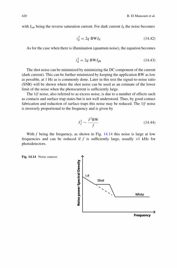
420 B. El Mansouri et al.
with Isat being the reverse saturation current. For dark current Id the noise becomes
i2d = 2q BWId (14.42)
As for the case when there is illumination (quantum noise), the equation becomes
i2d = 2q BWIph (14.43)
The shot noise can be minimized by minimizing the DC component of the current(dark current). This can be further minimized by keeping the application BW as lowas possible, at 1 Hz as is commonly done. Later in this text the signal-to-noise ratio(SNR) will be shown where the shot noise can be used as an estimate of the lowerlimit of the noise when the photocurrent is sufficiently large.
The 1/f noise, also referred to as excess noise, is due to a number of effects suchas contacts and surface trap states but is not well understood. Thus, by good contactfabrication and reduction of surface traps this noise may be reduced. The 1/f noiseis inversely proportional to the frequency and is given by
I 2f ∼ I 2BW
f(14.44)
With f being the frequency, as shown in Fig. 14.14 this noise is large at lowfrequencies and can be reduced if f is sufficiently large, usually >1 kHz forphotodetectors.
Fig. 14.14 Noise sources
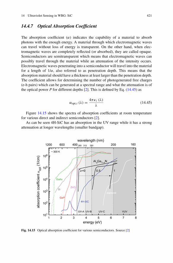
14 Ultraviolet Sensing in WBG: SiC 421
14.4.7 Optical Absorption Coefficient
The absorption coefficient (α) indicates the capability of a material to absorbphotons with the enough energy. A material through which electromagnetic wavescan travel without loss of energy is transparent. On the other hand, when elec-tromagnetic waves are completely reflected (or absorbed), they are called opaque.Semiconductors are semitransparent which means that electromagnetic waves canpossibly travel through the material while an attenuation of the intensity occurs.Electromagnetic waves penetrating into a semiconductor will travel into the materialfor a length of 1/α, also referred to as penetration depth. This means that theabsorption material should have a thickness at least larger than the penetration depth.The coefficient allows for determining the number of photogenerated free charges(e-h pairs) which can be generated at a spectral range and what the attenuation is ofthe optical power P for different depths [2]. This is defined by Eq. (14.45) as
αopt,i (λ) = 4πκi (λ)
λ(14.45)
Figure 14.15 shows the spectra of absorption coefficients at room temperaturefor various direct and indirect semiconductors [2].
As can be seen 4H-SiC has an absorption in the UV range while it has a strongattenuation at longer wavelengths (smaller bandgap).
Fig. 14.15 Optical absorption coefficient for various semiconductors. Source [2]
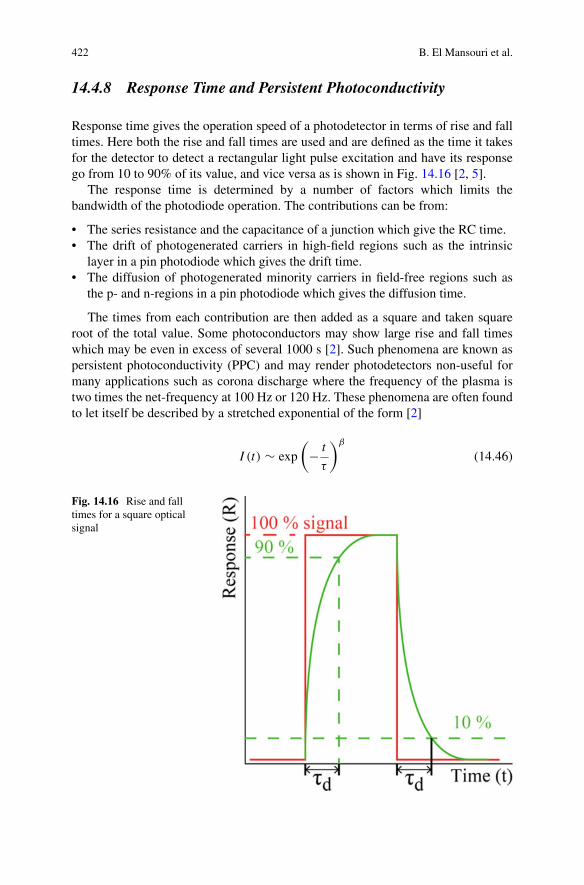
422 B. El Mansouri et al.
14.4.8 Response Time and Persistent Photoconductivity
Response time gives the operation speed of a photodetector in terms of rise and falltimes. Here both the rise and fall times are used and are defined as the time it takesfor the detector to detect a rectangular light pulse excitation and have its responsego from 10 to 90% of its value, and vice versa as is shown in Fig. 14.16 [2, 5].
The response time is determined by a number of factors which limits thebandwidth of the photodiode operation. The contributions can be from:
• The series resistance and the capacitance of a junction which give the RC time.• The drift of photogenerated carriers in high-field regions such as the intrinsic
layer in a pin photodiode which gives the drift time.• The diffusion of photogenerated minority carriers in field-free regions such as
the p- and n-regions in a pin photodiode which gives the diffusion time.
The times from each contribution are then added as a square and taken squareroot of the total value. Some photoconductors may show large rise and fall timeswhich may be even in excess of several 1000 s [2]. Such phenomena are known aspersistent photoconductivity (PPC) and may render photodetectors non-useful formany applications such as corona discharge where the frequency of the plasma istwo times the net-frequency at 100 Hz or 120 Hz. These phenomena are often foundto let itself be described by a stretched exponential of the form [2]
I (t) ∼ exp
(− t
τ
)β
(14.46)
Fig. 14.16 Rise and falltimes for a square opticalsignal

14 Ultraviolet Sensing in WBG: SiC 423
where τ is a time constant and 0 < β ≤ 1 is the Kohlrausch stretching parameter. Thelatter accounts for the microscopic nature of the electronic and atomic relaxationprocesses underlying the non-exponential change in measured conductivity [2].
14.4.9 Bandwidth
Bandwidth (BW) is defined as the frequency at which the photocurrent is (3 dB)lower than the low-frequency value [5]. This can be related to the decay time (τ ) forthe special case of exponential transient response by
BW = 1
2πτ= 2.20
2πτ d= 2.20
2πτ r(14.47)
As was shown in Fig. 14.16, to get a reliable result for the bandwidth, theexcitation pulse needs to be rectangular with a rise time much shorter and pulsewidth much larger than the rise time of the response, respectively. This is requiredin order for the photocurrent to reach a steady state value [5].
14.4.10 Linearity
The linearity between the photocurrent and the optical power incident on the activearea of the device is an important property which allows for a power-independentresponsivity (Rsp) as given by Eq. (14.31) and a reliable device operation [2]. Thelinearity is affected by a number of processes such as the carrier recombinationkinetics in the absorber material, the equivalent electrical circuit of the photodetectorand the readout circuit [2].
14.4.11 Dynamic Range
The dynamic range gives the range over which the detector response is linear withrespect to the incident light intensity [11].
14.5 Final Remarks
Optical detections are required in many applications, ranging from civil to militaryfields. Depending on the optical source, each sensing element needs to have distinctproperties with the spectral range at the top. Choices such as sensitivity and
424 B. El Mansouri et al.
environment play an equally important role, if not more important. The propertiesof the sensors can be tailored by selecting a proper material for a proper photode-tector device type. In this chapter, photodetection principles and requirements arediscussed, including design considerations and relevant parameters.
References
1. L. Sang, M. Liao, M. Sumiya, A comprehensive review of semiconductor ultraviolet photode-tectors: from thin film to one-dimensional nanostructures. Sensors 13, 10482 (2013)
2. M. Kneissl, J. Rass, III-nitride ultraviolet emitters, in Springer Series in Materials Science(Springer, 2016)
3. H. Chen, K. Liu, L. Hu, A.A. Al-Ghamdi, X. Fang, New concept ultraviolet photodetectors.Mater. Today 18, 493 (2015)
4. A. Aldalbahi, E. Li, M. Rivera, R. Velazquez, T. Altalhi, X. Peng, P.X. Feng, A new approachfor fabrications of SiC based photodetectors. Sci. Rep. 6, 23457 (2016)
5. E. Monroy, F. Omnès, F. Calle, Wide-bandgap semiconductor ultraviolet photodetectors.Semicond. Sci. Technol. 18, R33 (2003)
6. L. Luo, Y. Zhang, S.S. Mao, L. Lin, Fabrication and characterization of ZnO nanowires basedUV photodiodes. Sensors Actuators A Phys. 127, 201 (2006)
7. G. Li, J. Zhang, X. Hou, Temperature dependence of performance of ZnO-based metal-semiconductor-metal ultraviolet photodetectors. Sensors Actuators A Phys. 209, 149 (2014)
8. Z. Zhang, W. Zhang, D. Zhang, Y. Xiao, J. Deng, G. Xia, Comparison of different characteristicparameters acquired by UV imager in detecting corona discharge. IEEE Trans. Dielectr. Electr.Insul. 23, 1597 (2016)
9. T. Okino, S. Yamahira, S. Yamada, Y. Hirose, A. Odagawa, Y. Kato, T. Tanaka, Ultravioletand visible spectral imaging of hydrogen flames using an organic photoconductive film CMOSimager, in Proceedings of the International Image SensorWorkshop, Hiroshima, vol. 30 (2017),pp. 188–191
10. T. Okino, S. Yamahira, S. Yamada, Y. Hirose, A. Odagawa, Y. Kato, T. Tanaka, A real-timeultraviolet radiation imaging system using an organic photoconductive image sensor. Sensors18, 314 (2018)
11. T.D. Moustakas, R. Paiella, Optoelectronic device physics and technology of nitride semicon-ductors from the UV to the terahertz. Rep. Prog. Phys. 80, 106501 (2017)
12. S. Shinde, C. Bhosale, K. Rajpure, N-doped ZnO based fast response ultraviolet photoconduc-tive detector. Solid State Electron. 68, 22 (2012)
13. E. Munoz, E. Monroy, J. Pau, F. Calle, F. Omnes, P. Gibart, III nitrides and UV detection. J.Phys. Condens. Matter 13, 7115 (2001)
14. Y. Duan, M. Cong, D. Jiang, Z. Guo, X. Zhou, N. Hu, K. Yu, ZnO ultraviolet photodetector-based metal-semiconductor-metal structure, in Young Scientists Forum 2017, vol. 10710(International Society for Optics and Photonics, 2018), p. 107100X
15. H.-P. Lin, X.-J. Lin, D.-C. Perng, Electrodeposited CuSCN metal-semiconductor metal highperformance deep-ultraviolet photodetector. Appl. Phys. Lett. 112, 021107 (2018)
16. H. Ferhati, F. Djeffal, New high performance ultraviolet (MSM) TiO2/glass photodetectorbased on diffraction grating for optoelectronic applications. Optik Int. J. Light Electron Opt.127, 7202 (2016)
17. S. Mohammadnejad, S.E. Maklavani, E. Rahimi, Dark current reduction in ZnO based MSMphotodetectors with interfacial thin oxide layer, in International Symposium on High CapacityOptical Networks and Enabling Technologies, 2008 (HONET 2008) (IEEE, 2008), pp. 259–264

14 Ultraviolet Sensing in WBG: SiC 425
18. X. Yang, D. Jiang, Z. Guo, W. Zhang, N. Hu, Y. Duan, S. Gao, Q. Liang, T. Zheng, J. Lv,Improving performance of the MgZnO ultraviolet photodetectors by changing the interdigitalelectrode width. Mater. Res. Bull. 98, 275 (2018)
19. H.-Y. Chen, K.-W. Liu, X. Chen, Z.-Z. Zhang, M.-M. Fan, M.-M. Jiang, X.-H. Xie, H.-F. Zhao,D.-Z. Shen, Realization of a self-powered ZnO MSM UV photodetector with high responsivityusing an asymmetric pair of au electrodes. J. Mater. Chem. C 2, 9689 (2014)
20. J. Edmond, H. Kong, A. Suvorov, D. Waltz, C. Carter Jr., 6H-silicon carbide light emittingdiodes and UV photodiodes. Phys. Status Solidi (a) 162, 481 (1997)
21. X. Chen, H. Zhu, J. Cai, Z. Wu, High-performance 4H-SiC-based ultraviolet p-i-n photodetec-tor. J. Appl. Phys. 102, 024505 (2007)
22. S. Biondo, M. Lazar, L. Ottaviani, W. Vervisch, V. Le Borgne, M.A. El Khakani, J. Duchaine, F.Milesi, O. Palais, D. Planson, 4H-silicon carbide thin junction based ultraviolet photodetectors.Thin Solid Films 522, 17 (2012)
23. H. Zhu, X. Chen, J. Cai, Z. Wu, 4H–SiC ultraviolet avalanche photodetectors with lowbreakdown voltage and high gain. Solid State Electron. 53, 7 (2009)
24. X. Bai, X. Guo, D.C. Mcintosh, H.-D. Liu, J.C. Campbell, High detection sensitivity ofultraviolet 4H-SiC avalanche photodiodes. IEEE J. Quantum Electron. 43, 1159 (2007)
25. H. Liu, D. Mcintosh, X. Bai, H. Pan, M. Liu, J.C. Campbell, H.Y. Cha, 4H-SiC pin recessed-window avalanche photodiode with high quantum efficiency. IEEE Photon. Technol. Lett. 20,1551 (2008)
Chapter 15Integrated Photonic Microsystems
J. Kjellman, N. Hosseini, Jeong Hwan Song, T. Tongnyuy, S. Dwivedi,B. Troia, B. Figeys, S. Kerman, A. Stassen, P. Neutens, S. Severi, R. Jansen,P. Soussan, S. S. Saseendran, A. Marinins, and X. Rottenberg
15.1 Introduction
Photonics, the science of generating and/or processing light at the wavelength-scale, e.g., micro/nanometer-scale, is enabling evermore applications, includingLED-lighting, fiber-to-the-home internet, solar panels, displays, and image sensors.Recent progress in nano-fabrication now also allows to produce large-scale photoniccircuits on wafer-scale with CMOS-compatible processes, providing cost-effectivehigh-quality optical systems.
The development of these wafer-scale photonics platforms was first led by theever-increasing requirements of bandwidth for high-speed communication. Theincrease in complexity of the optical interconnections forced indeed to considermoving away from fiber-based macrosystems to microchip-based ones, reproducingin compact form factor and at low costs the functions of bulky, failure-prone andexpensive optical macrosystems. The key platform technology for this was and stillis Si-photonics [1].
Recently, the maturing integrated photonics platforms emerge as key enablers fora novel family of more diverse applications. In particular, the hybridization of Si-photonics platforms with novel material systems, e.g., SiN-core waveguides, opensbroader wavelength reach than previously addressed. SiN can indeed be used toguide light on-chip across the visible and through the NIR, extending till ∼8 μm.SiN is instrumental to enable for example industrial and biomedical sensing [2](Fig. 15.1).
J. Kjellman · N. Hosseini · J. H. Song · T. Tongnyuy · S. Dwivedi · B. Troia · B. FigeysS. Kerman · A. Stassen · P. Neutens · S. Severi · R. Jansen · P. Soussan · S. S. SaseendranA. Marinins · X. Rottenberg (�)IMEC, Leuven, Belgiume-mail: [email protected]
© Springer Nature Switzerland AG 2020W. D. van Driel et al. (eds.), Sensor Systems Simulations,https://doi.org/10.1007/978-3-030-16577-2_15
427
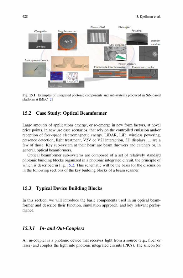
428 J. Kjellman et al.
Fig. 15.1 Examples of integrated photonic components and sub-systems produced in SiN-basedplatform at IMEC [2]
15.2 Case Study: Optical Beamformer
Large amounts of applications emerge, or re-emerge in new form factors, at novelprice points, in new use case scenarios, that rely on the controlled emission and/orreception of free-space electromagnetic energy. LiDAR, LiFi, wireless powering,presence detection, light treatment, V2V or V2I interaction, 3D displays, ... are afew of those. Key sub-system at their heart are beam throwers and catchers or, ingeneral, optical beamformers.
Optical beamformer sub-systems are composed of a set of relatively standardphotonic building blocks organized in a photonic integrated circuit, the principle ofwhich is described in Fig. 15.2. This schematic will be the basis for the discussionin the following sections of the key building blocks of a beam scanner.
15.3 Typical Device Building Blocks
In this section, we will introduce the basic components used in an optical beam-former and describe their function, simulation approach, and key relevant perfor-mance.
15.3.1 In- and Out-Couplers
An in-coupler is a photonic device that receives light from a source (e.g., fiber orlaser) and couples the light into photonic integrated circuits (PICs). The silicon (or
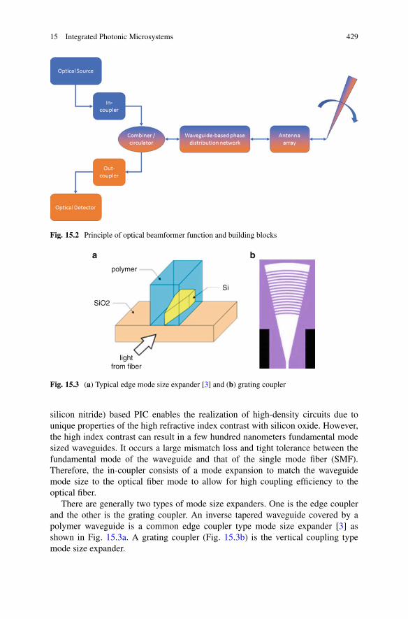
15 Integrated Photonic Microsystems 429
Fig. 15.2 Principle of optical beamformer function and building blocks
polymer
SiO2
lightfrom fiber
a b
Si
Fig. 15.3 (a) Typical edge mode size expander [3] and (b) grating coupler
silicon nitride) based PIC enables the realization of high-density circuits due tounique properties of the high refractive index contrast with silicon oxide. However,the high index contrast can result in a few hundred nanometers fundamental modesized waveguides. It occurs a large mismatch loss and tight tolerance between thefundamental mode of the waveguide and that of the single mode fiber (SMF).Therefore, the in-coupler consists of a mode expansion to match the waveguidemode size to the optical fiber mode to allow for high coupling efficiency to theoptical fiber.
There are generally two types of mode size expanders. One is the edge couplerand the other is the grating coupler. An inverse tapered waveguide covered by apolymer waveguide is a common edge coupler type mode size expander [3] asshown in Fig. 15.3a. A grating coupler (Fig. 15.3b) is the vertical coupling typemode size expander.
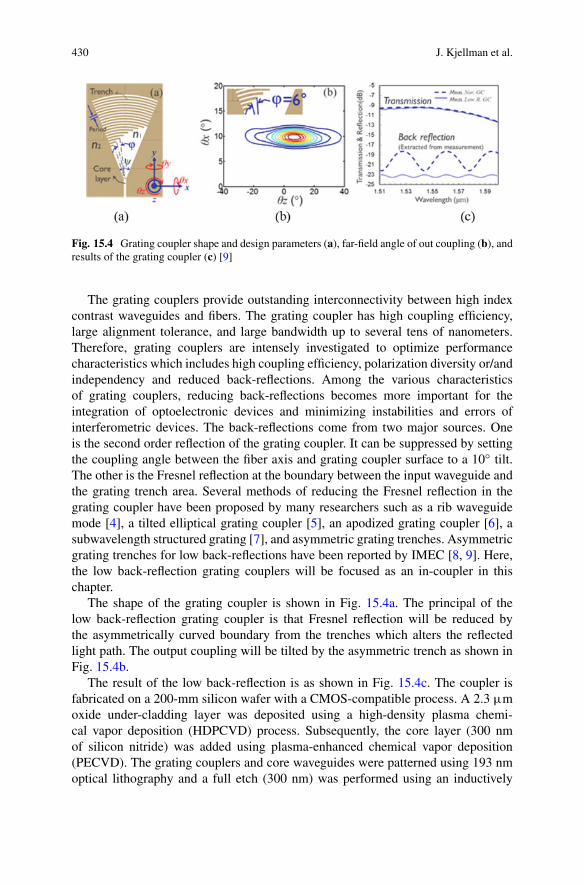
430 J. Kjellman et al.
Fig. 15.4 Grating coupler shape and design parameters (a), far-field angle of out coupling (b), andresults of the grating coupler (c) [9]
The grating couplers provide outstanding interconnectivity between high indexcontrast waveguides and fibers. The grating coupler has high coupling efficiency,large alignment tolerance, and large bandwidth up to several tens of nanometers.Therefore, grating couplers are intensely investigated to optimize performancecharacteristics which includes high coupling efficiency, polarization diversity or/andindependency and reduced back-reflections. Among the various characteristicsof grating couplers, reducing back-reflections becomes more important for theintegration of optoelectronic devices and minimizing instabilities and errors ofinterferometric devices. The back-reflections come from two major sources. Oneis the second order reflection of the grating coupler. It can be suppressed by settingthe coupling angle between the fiber axis and grating coupler surface to a 10◦ tilt.The other is the Fresnel reflection at the boundary between the input waveguide andthe grating trench area. Several methods of reducing the Fresnel reflection in thegrating coupler have been proposed by many researchers such as a rib waveguidemode [4], a tilted elliptical grating coupler [5], an apodized grating coupler [6], asubwavelength structured grating [7], and asymmetric grating trenches. Asymmetricgrating trenches for low back-reflections have been reported by IMEC [8, 9]. Here,the low back-reflection grating couplers will be focused as an in-coupler in thischapter.
The shape of the grating coupler is shown in Fig. 15.4a. The principal of thelow back-reflection grating coupler is that Fresnel reflection will be reduced bythe asymmetrically curved boundary from the trenches which alters the reflectedlight path. The output coupling will be tilted by the asymmetric trench as shown inFig. 15.4b.
The result of the low back-reflection is as shown in Fig. 15.4c. The coupler isfabricated on a 200-mm silicon wafer with a CMOS-compatible process. A 2.3 μmoxide under-cladding layer was deposited using a high-density plasma chemi-cal vapor deposition (HDPCVD) process. Subsequently, the core layer (300 nmof silicon nitride) was added using plasma-enhanced chemical vapor deposition(PECVD). The grating couplers and core waveguides were patterned using 193 nmoptical lithography and a full etch (300 nm) was performed using an inductively
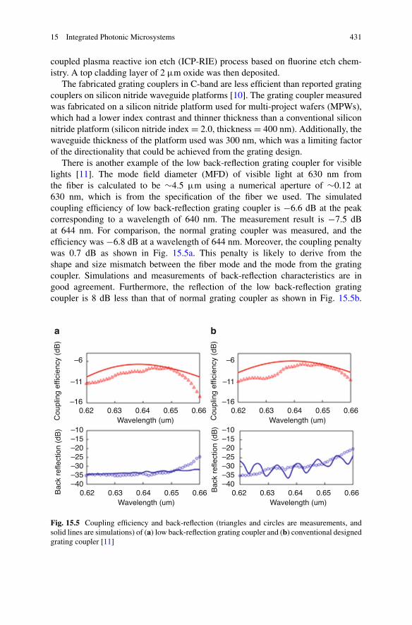
15 Integrated Photonic Microsystems 431
coupled plasma reactive ion etch (ICP-RIE) process based on fluorine etch chem-istry. A top cladding layer of 2 μm oxide was then deposited.
The fabricated grating couplers in C-band are less efficient than reported gratingcouplers on silicon nitride waveguide platforms [10]. The grating coupler measuredwas fabricated on a silicon nitride platform used for multi-project wafers (MPWs),which had a lower index contrast and thinner thickness than a conventional siliconnitride platform (silicon nitride index = 2.0, thickness = 400 nm). Additionally, thewaveguide thickness of the platform used was 300 nm, which was a limiting factorof the directionality that could be achieved from the grating design.
There is another example of the low back-reflection grating coupler for visiblelights [11]. The mode field diameter (MFD) of visible light at 630 nm fromthe fiber is calculated to be ∼4.5 μm using a numerical aperture of ∼0.12 at630 nm, which is from the specification of the fiber we used. The simulatedcoupling efficiency of low back-reflection grating coupler is −6.6 dB at the peakcorresponding to a wavelength of 640 nm. The measurement result is −7.5 dBat 644 nm. For comparison, the normal grating coupler was measured, and theefficiency was −6.8 dB at a wavelength of 644 nm. Moreover, the coupling penaltywas 0.7 dB as shown in Fig. 15.5a. This penalty is likely to derive from theshape and size mismatch between the fiber mode and the mode from the gratingcoupler. Simulations and measurements of back-reflection characteristics are ingood agreement. Furthermore, the reflection of the low back-reflection gratingcoupler is 8 dB less than that of normal grating coupler as shown in Fig. 15.5b.
0.62–16
–11
–6
Cou
plin
g ef
ficie
ncy
(dB
)
0.63 0.64Wavelength (um)
0.65 0.66
a
0.62–16
–11
–6
Cou
plin
g ef
ficie
ncy
(dB
)
0.63 0.64Wavelength (um)
0.65 0.66
0.62–40–35–30–25–20–15–10
–40–35–30–25–20–15–10
Bac
k re
flect
ion
(dB
)
0.63 0.64Wavelength (um)
0.65 0.66 0.62Bac
k re
flect
ion
(dB
)
0.63 0.64Wavelength (um)
0.65 0.66
b
Fig. 15.5 Coupling efficiency and back-reflection (triangles and circles are measurements, andsolid lines are simulations) of (a) low back-reflection grating coupler and (b) conventional designedgrating coupler [11]
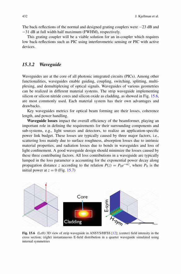
432 J. Kjellman et al.
The back-reflections of the normal and designed grating couplers were −23 dB and−31 dB at full width half maximum (FWHM), respectively.
This grating coupler will be a viable solution for an in-coupler which requireslow back-reflections such as PIC using interferometric sensing or PIC with activedevices.
15.3.2 Waveguide
Waveguides are at the core of all photonic integrated circuits (PICs). Among otherfunctionalities, waveguides enable guiding, coupling, switching, splitting, multi-plexing, and demultiplexing of optical signals. Waveguides of various geometriescan be realized in different material systems. The strip waveguide implementingsilicon or silicon nitride cores and silicon oxide as cladding, as showed in Fig. 15.6,are most commonly used. Each material system has their own advantages anddrawbacks.
Key waveguides metrics for optical beam forming are their losses, coherencelength, and power handling.
Waveguide losses impact the overall efficiency of the beamformer, playing animportant role in defining the requirements for their surrounding components andsub-systems, e.g., light sources and detectors, to realize an application-specificpower link budget. These losses are typically caused by three major factors, i.e.,scattering loss mainly due to surface roughness, absorption losses due to intrinsicmaterial properties, and radiation losses due to bends in waveguides and loss oflight confinement. A good waveguide design should minimize the losses caused bythese three contributing factors. All loss contributions in a waveguide are typicallylumped in the loss parameter α accounting for the exponential power decay alongpropagation distance z according to the relation P(z) = P0e−αz, where P0 is theinitial power at z = 0 (Fig. 15.7)
Fig. 15.6 (Left) 3D view of strip waveguide in ANSYS/HFSS [12]; (center) field intensity in thecross section; (right) instantaneous E-field distribution in a quarter waveguide simulated usinginternal symmetries
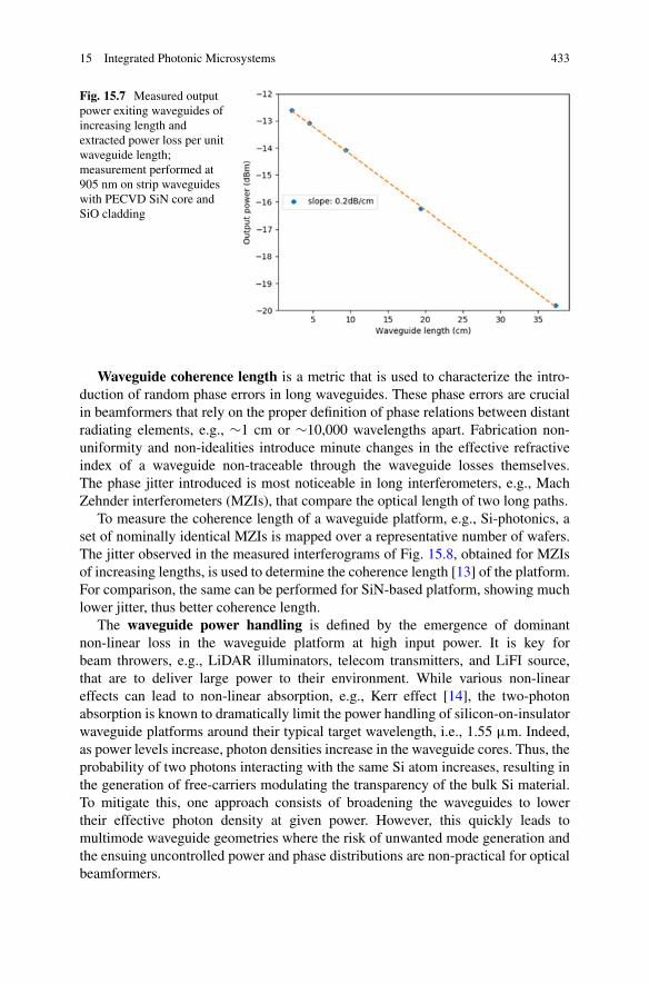
15 Integrated Photonic Microsystems 433
Fig. 15.7 Measured outputpower exiting waveguides ofincreasing length andextracted power loss per unitwaveguide length;measurement performed at905 nm on strip waveguideswith PECVD SiN core andSiO cladding
Waveguide coherence length is a metric that is used to characterize the intro-duction of random phase errors in long waveguides. These phase errors are crucialin beamformers that rely on the proper definition of phase relations between distantradiating elements, e.g., ∼1 cm or ∼10,000 wavelengths apart. Fabrication non-uniformity and non-idealities introduce minute changes in the effective refractiveindex of a waveguide non-traceable through the waveguide losses themselves.The phase jitter introduced is most noticeable in long interferometers, e.g., MachZehnder interferometers (MZIs), that compare the optical length of two long paths.
To measure the coherence length of a waveguide platform, e.g., Si-photonics, aset of nominally identical MZIs is mapped over a representative number of wafers.The jitter observed in the measured interferograms of Fig. 15.8, obtained for MZIsof increasing lengths, is used to determine the coherence length [13] of the platform.For comparison, the same can be performed for SiN-based platform, showing muchlower jitter, thus better coherence length.
The waveguide power handling is defined by the emergence of dominantnon-linear loss in the waveguide platform at high input power. It is key forbeam throwers, e.g., LiDAR illuminators, telecom transmitters, and LiFI source,that are to deliver large power to their environment. While various non-lineareffects can lead to non-linear absorption, e.g., Kerr effect [14], the two-photonabsorption is known to dramatically limit the power handling of silicon-on-insulatorwaveguide platforms around their typical target wavelength, i.e., 1.55 μm. Indeed,as power levels increase, photon densities increase in the waveguide cores. Thus, theprobability of two photons interacting with the same Si atom increases, resulting inthe generation of free-carriers modulating the transparency of the bulk Si material.To mitigate this, one approach consists of broadening the waveguides to lowertheir effective photon density at given power. However, this quickly leads tomultimode waveguide geometries where the risk of unwanted mode generation andthe ensuing uncontrolled power and phase distributions are non-practical for opticalbeamformers.
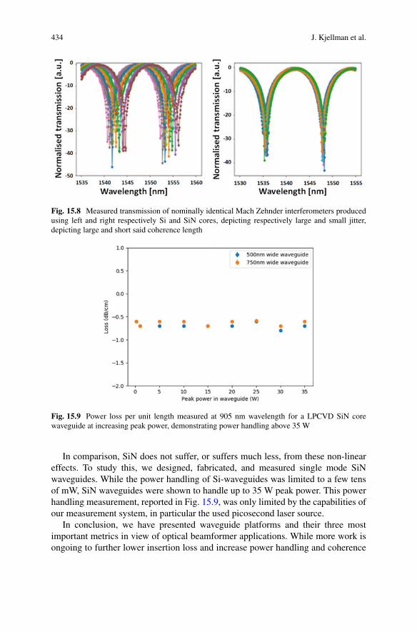
434 J. Kjellman et al.
Fig. 15.8 Measured transmission of nominally identical Mach Zehnder interferometers producedusing left and right respectively Si and SiN cores, depicting respectively large and small jitter,depicting large and short said coherence length
Fig. 15.9 Power loss per unit length measured at 905 nm wavelength for a LPCVD SiN corewaveguide at increasing peak power, demonstrating power handling above 35 W
In comparison, SiN does not suffer, or suffers much less, from these non-lineareffects. To study this, we designed, fabricated, and measured single mode SiNwaveguides. While the power handling of Si-waveguides was limited to a few tensof mW, SiN waveguides were shown to handle up to 35 W peak power. This powerhandling measurement, reported in Fig. 15.9, was only limited by the capabilities ofour measurement system, in particular the used picosecond laser source.
In conclusion, we have presented waveguide platforms and their three mostimportant metrics in view of optical beamformer applications. While more work isongoing to further lower insertion loss and increase power handling and coherence
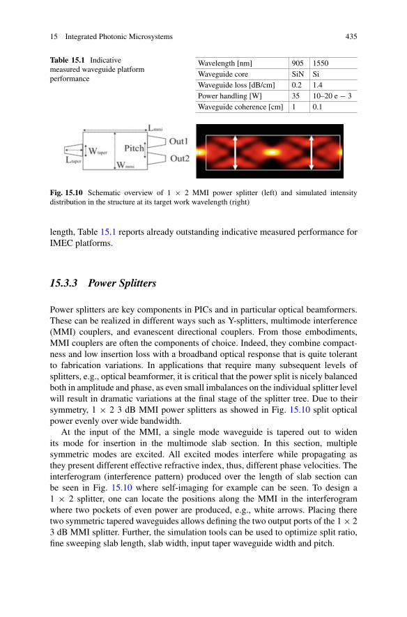
15 Integrated Photonic Microsystems 435
Table 15.1 Indicativemeasured waveguide platformperformance
Wavelength [nm] 905 1550Waveguide core SiN SiWaveguide loss [dB/cm] 0.2 1.4Power handling [W] 35 10–20 e − 3Waveguide coherence [cm] 1 0.1
Fig. 15.10 Schematic overview of 1 × 2 MMI power splitter (left) and simulated intensitydistribution in the structure at its target work wavelength (right)
length, Table 15.1 reports already outstanding indicative measured performance forIMEC platforms.
15.3.3 Power Splitters
Power splitters are key components in PICs and in particular optical beamformers.These can be realized in different ways such as Y-splitters, multimode interference(MMI) couplers, and evanescent directional couplers. From those embodiments,MMI couplers are often the components of choice. Indeed, they combine compact-ness and low insertion loss with a broadband optical response that is quite tolerantto fabrication variations. In applications that require many subsequent levels ofsplitters, e.g., optical beamformer, it is critical that the power split is nicely balancedboth in amplitude and phase, as even small imbalances on the individual splitter levelwill result in dramatic variations at the final stage of the splitter tree. Due to theirsymmetry, 1 × 2 3 dB MMI power splitters as showed in Fig. 15.10 split opticalpower evenly over wide bandwidth.
At the input of the MMI, a single mode waveguide is tapered out to widenits mode for insertion in the multimode slab section. In this section, multiplesymmetric modes are excited. All excited modes interfere while propagating asthey present different effective refractive index, thus, different phase velocities. Theinterferogram (interference pattern) produced over the length of slab section canbe seen in Fig. 15.10 where self-imaging for example can be seen. To design a1 × 2 splitter, one can locate the positions along the MMI in the interferogramwhere two pockets of even power are produced, e.g., white arrows. Placing theretwo symmetric tapered waveguides allows defining the two output ports of the 1 × 23 dB MMI splitter. Further, the simulation tools can be used to optimize split ratio,fine sweeping slab length, slab width, input taper waveguide width and pitch.
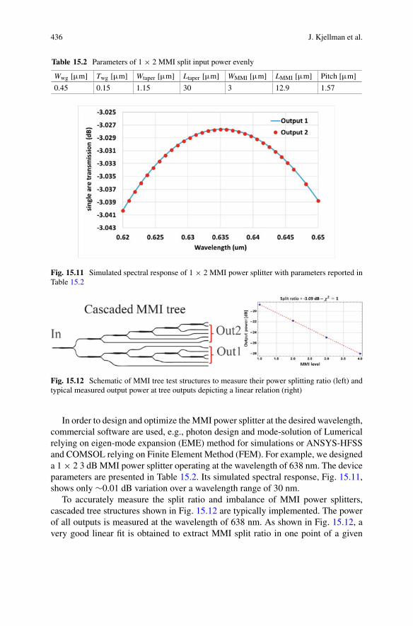
436 J. Kjellman et al.
Table 15.2 Parameters of 1 × 2 MMI split input power evenly
Wwg [μm] Twg [μm] Wtaper [μm] Ltaper [μm] WMMI [μm] LMMI [μm] Pitch [μm]
0.45 0.15 1.15 30 3 12.9 1.57
Fig. 15.11 Simulated spectral response of 1 × 2 MMI power splitter with parameters reported inTable 15.2
Fig. 15.12 Schematic of MMI tree test structures to measure their power splitting ratio (left) andtypical measured output power at tree outputs depicting a linear relation (right)
In order to design and optimize the MMI power splitter at the desired wavelength,commercial software are used, e.g., photon design and mode-solution of Lumericalrelying on eigen-mode expansion (EME) method for simulations or ANSYS-HFSSand COMSOL relying on Finite Element Method (FEM). For example, we designeda 1 × 2 3 dB MMI power splitter operating at the wavelength of 638 nm. The deviceparameters are presented in Table 15.2. Its simulated spectral response, Fig. 15.11,shows only ∼0.01 dB variation over a wavelength range of 30 nm.
To accurately measure the split ratio and imbalance of MMI power splitters,cascaded tree structures shown in Fig. 15.12 are typically implemented. The powerof all outputs is measured at the wavelength of 638 nm. As shown in Fig. 15.12, avery good linear fit is obtained to extract MMI split ratio in one point of a given
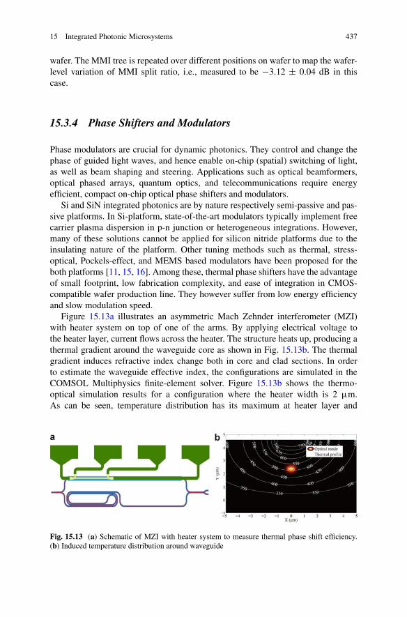
15 Integrated Photonic Microsystems 437
wafer. The MMI tree is repeated over different positions on wafer to map the wafer-level variation of MMI split ratio, i.e., measured to be −3.12 ± 0.04 dB in thiscase.
15.3.4 Phase Shifters and Modulators
Phase modulators are crucial for dynamic photonics. They control and change thephase of guided light waves, and hence enable on-chip (spatial) switching of light,as well as beam shaping and steering. Applications such as optical beamformers,optical phased arrays, quantum optics, and telecommunications require energyefficient, compact on-chip optical phase shifters and modulators.
Si and SiN integrated photonics are by nature respectively semi-passive and pas-sive platforms. In Si-platform, state-of-the-art modulators typically implement freecarrier plasma dispersion in p-n junction or heterogeneous integrations. However,many of these solutions cannot be applied for silicon nitride platforms due to theinsulating nature of the platform. Other tuning methods such as thermal, stress-optical, Pockels-effect, and MEMS based modulators have been proposed for theboth platforms [11, 15, 16]. Among these, thermal phase shifters have the advantageof small footprint, low fabrication complexity, and ease of integration in CMOS-compatible wafer production line. They however suffer from low energy efficiencyand slow modulation speed.
Figure 15.13a illustrates an asymmetric Mach Zehnder interferometer (MZI)with heater system on top of one of the arms. By applying electrical voltage tothe heater layer, current flows across the heater. The structure heats up, producing athermal gradient around the waveguide core as shown in Fig. 15.13b. The thermalgradient induces refractive index change both in core and clad sections. In orderto estimate the waveguide effective index, the configurations are simulated in theCOMSOL Multiphysics finite-element solver. Figure 15.13b shows the thermo-optical simulation results for a configuration where the heater width is 2 μm.As can be seen, temperature distribution has its maximum at heater layer and
Fig. 15.13 (a) Schematic of MZI with heater system to measure thermal phase shift efficiency.(b) Induced temperature distribution around waveguide
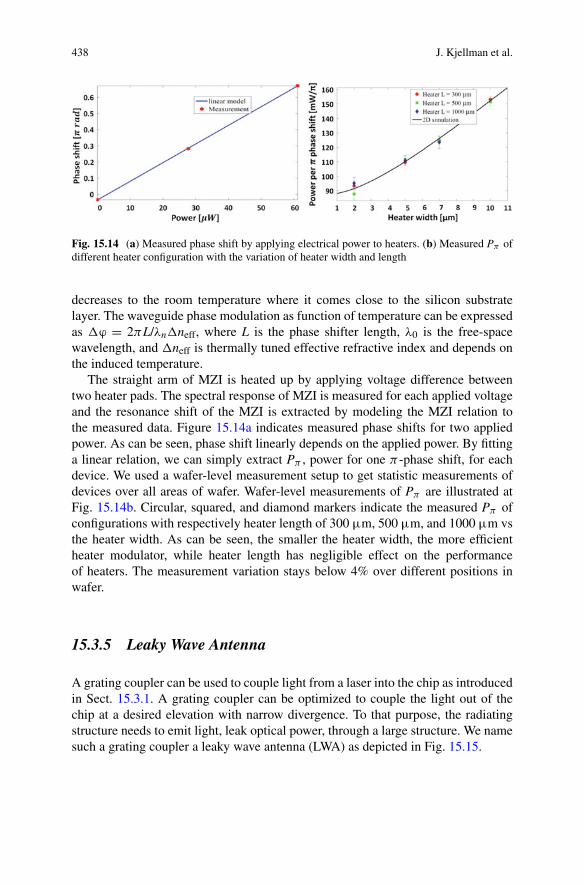
438 J. Kjellman et al.
Fig. 15.14 (a) Measured phase shift by applying electrical power to heaters. (b) Measured Pπ ofdifferent heater configuration with the variation of heater width and length
decreases to the room temperature where it comes close to the silicon substratelayer. The waveguide phase modulation as function of temperature can be expressedas ϕ = 2πL/λnneff, where L is the phase shifter length, λ0 is the free-spacewavelength, and neff is thermally tuned effective refractive index and depends onthe induced temperature.
The straight arm of MZI is heated up by applying voltage difference betweentwo heater pads. The spectral response of MZI is measured for each applied voltageand the resonance shift of the MZI is extracted by modeling the MZI relation tothe measured data. Figure 15.14a indicates measured phase shifts for two appliedpower. As can be seen, phase shift linearly depends on the applied power. By fittinga linear relation, we can simply extract Pπ , power for one π -phase shift, for eachdevice. We used a wafer-level measurement setup to get statistic measurements ofdevices over all areas of wafer. Wafer-level measurements of Pπ are illustrated atFig. 15.14b. Circular, squared, and diamond markers indicate the measured Pπ ofconfigurations with respectively heater length of 300 μm, 500 μm, and 1000 μm vsthe heater width. As can be seen, the smaller the heater width, the more efficientheater modulator, while heater length has negligible effect on the performanceof heaters. The measurement variation stays below 4% over different positions inwafer.
15.3.5 Leaky Wave Antenna
A grating coupler can be used to couple light from a laser into the chip as introducedin Sect. 15.3.1. A grating coupler can be optimized to couple the light out of thechip at a desired elevation with narrow divergence. To that purpose, the radiatingstructure needs to emit light, leak optical power, through a large structure. We namesuch a grating coupler a leaky wave antenna (LWA) as depicted in Fig. 15.15.
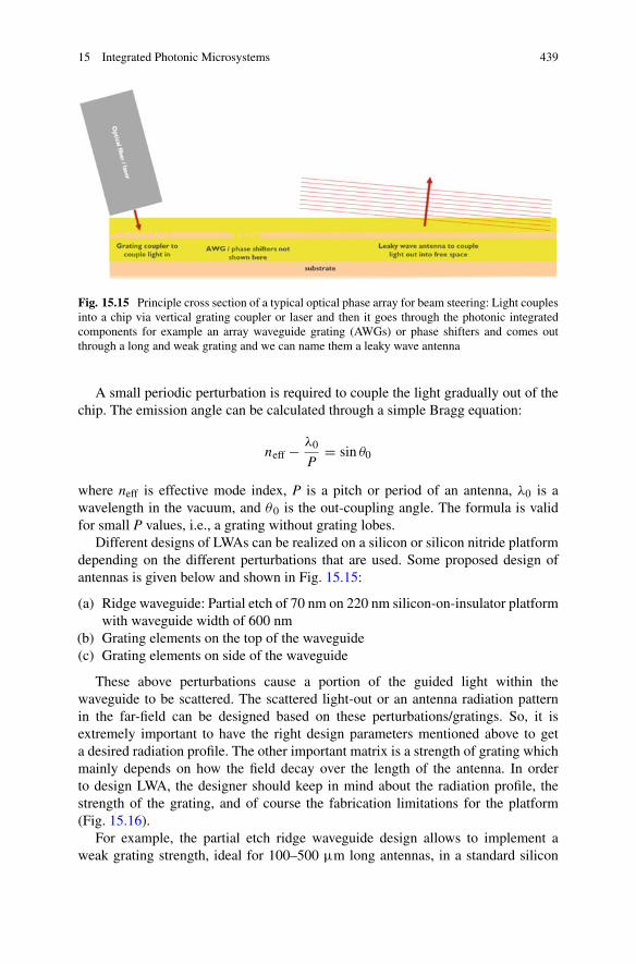
15 Integrated Photonic Microsystems 439
Fig. 15.15 Principle cross section of a typical optical phase array for beam steering: Light couplesinto a chip via vertical grating coupler or laser and then it goes through the photonic integratedcomponents for example an array waveguide grating (AWGs) or phase shifters and comes outthrough a long and weak grating and we can name them a leaky wave antenna
A small periodic perturbation is required to couple the light gradually out of thechip. The emission angle can be calculated through a simple Bragg equation:
neff − λ0
P= sin θ0
where neff is effective mode index, P is a pitch or period of an antenna, λ0 is awavelength in the vacuum, and θ0 is the out-coupling angle. The formula is validfor small P values, i.e., a grating without grating lobes.
Different designs of LWAs can be realized on a silicon or silicon nitride platformdepending on the different perturbations that are used. Some proposed design ofantennas is given below and shown in Fig. 15.15:
(a) Ridge waveguide: Partial etch of 70 nm on 220 nm silicon-on-insulator platformwith waveguide width of 600 nm
(b) Grating elements on the top of the waveguide(c) Grating elements on side of the waveguide
These above perturbations cause a portion of the guided light within thewaveguide to be scattered. The scattered light-out or an antenna radiation patternin the far-field can be designed based on these perturbations/gratings. So, it isextremely important to have the right design parameters mentioned above to geta desired radiation profile. The other important matrix is a strength of grating whichmainly depends on how the field decay over the length of the antenna. In orderto design LWA, the designer should keep in mind about the radiation profile, thestrength of the grating, and of course the fabrication limitations for the platform(Fig. 15.16).
For example, the partial etch ridge waveguide design allows to implement aweak grating strength, ideal for 100–500 μm long antennas, in a standard silicon
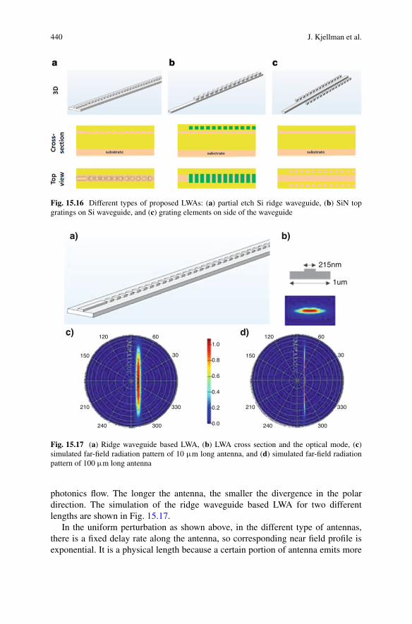
440 J. Kjellman et al.
Fig. 15.16 Different types of proposed LWAs: (a) partial etch Si ridge waveguide, (b) SiN topgratings on Si waveguide, and (c) grating elements on side of the waveguide
215nm
a) b)
c) d)
1um
120 60
30
330
300240
210
150
120 60
30
1.0
0.8
0.6
0.4
0.2
0.0
330
300240
210
150
Fig. 15.17 (a) Ridge waveguide based LWA, (b) LWA cross section and the optical mode, (c)simulated far-field radiation pattern of 10 μm long antenna, and (d) simulated far-field radiationpattern of 100 μm long antenna
photonics flow. The longer the antenna, the smaller the divergence in the polardirection. The simulation of the ridge waveguide based LWA for two differentlengths are shown in Fig. 15.17.
In the uniform perturbation as shown above, in the different type of antennas,there is a fixed delay rate along the antenna, so corresponding near field profile isexponential. It is a physical length because a certain portion of antenna emits more
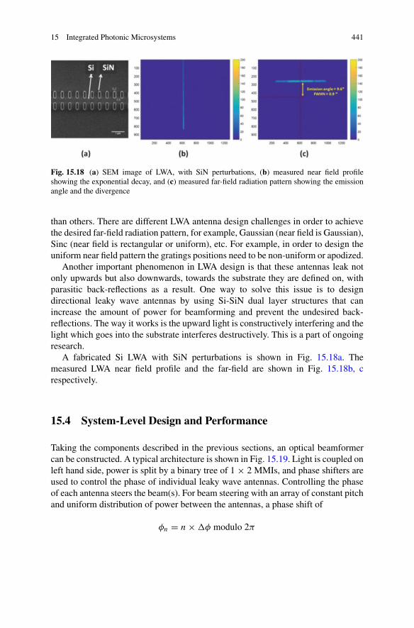
15 Integrated Photonic Microsystems 441
Fig. 15.18 (a) SEM image of LWA, with SiN perturbations, (b) measured near field profileshowing the exponential decay, and (c) measured far-field radiation pattern showing the emissionangle and the divergence
than others. There are different LWA antenna design challenges in order to achievethe desired far-field radiation pattern, for example, Gaussian (near field is Gaussian),Sinc (near field is rectangular or uniform), etc. For example, in order to design theuniform near field pattern the gratings positions need to be non-uniform or apodized.
Another important phenomenon in LWA design is that these antennas leak notonly upwards but also downwards, towards the substrate they are defined on, withparasitic back-reflections as a result. One way to solve this issue is to designdirectional leaky wave antennas by using Si-SiN dual layer structures that canincrease the amount of power for beamforming and prevent the undesired back-reflections. The way it works is the upward light is constructively interfering and thelight which goes into the substrate interferes destructively. This is a part of ongoingresearch.
A fabricated Si LWA with SiN perturbations is shown in Fig. 15.18a. Themeasured LWA near field profile and the far-field are shown in Fig. 15.18b, crespectively.
15.4 System-Level Design and Performance
Taking the components described in the previous sections, an optical beamformercan be constructed. A typical architecture is shown in Fig. 15.19. Light is coupled onleft hand side, power is split by a binary tree of 1 × 2 MMIs, and phase shifters areused to control the phase of individual leaky wave antennas. Controlling the phaseof each antenna steers the beam(s). For beam steering with an array of constant pitchand uniform distribution of power between the antennas, a phase shift of
φn = n × φ modulo 2π
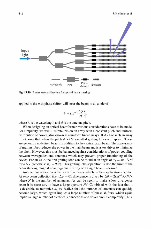
442 J. Kjellman et al.
Fig. 15.19 Binary tree architecture for optical beam steering
applied to the n-th phase shifter will steer the beam to an angle of
θ = sin−1 φ
2π
λ
d,
where λ is the wavelength and d is the antenna pitch.When designing an optical beamformer, various considerations have to be made.
For simplicity, we will illustrate this on an array with a constant pitch and uniformdistribution of power, also known as a uniform linear array (ULA). For such an arrayit is known that when the pitch d > λ/2 so-called grating lobes will appear. Theseare generally undesired beams in addition to the central main beam. The appearanceof grating lobes reduces the power in the main beam and is a key driver to minimizethe pitch. However, this must be balanced against considerations of power couplingbetween waveguides and antennas which may prevent proper functioning of thedevice. For an ULA the first grating lobe can be found at an angle of θ1 = sin−1λ/dfor d > λ (otherwise θ1 = 90◦). This grating lobe separation is also the limit of thebeam steering range if unambiguous steering of a single beam is desired.
Another consideration is the beam divergence which is often application specific.At zero beam deflection (i.e., φ = 0), divergence is given by θ = 2sin−1λ/(Nd),where N is the number of antennas. As can be seen, to make a low divergencebeam it is necessary to have a large aperture Nd. Combined with the fact that itis desirable to minimize d, we realize that the number of antennas can quicklybecome large, which again implies a large number of phase shifters, which againimplies a large number of electrical connections and driver circuit complexity. Thus,
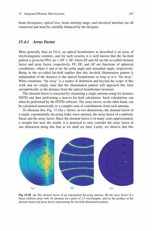
15 Integrated Photonic Microsystems 443
beam divergence, optical loss, beam steering range, and electrical interface are allconnected and must be carefully balanced by the designer.
15.4.1 Array Factor
More generally than an ULA, an optical beamformer as described is an array ofelectromagnetic emitters, and for such systems it is well known that the far-fieldpattern is given by FF(θ , φ) = EF × AF, where EF and AF are the so-called elementfactor and array factor, respectively. FF, EF, and AF are functions of sphericalcoordinates, where θ and φ are the polar angle and azimuthal angle, respectively.Being in the so-called far-field implies that this far-field illumination pattern isindependent of the distance to the optical beamformer as long as it is “far away.”What constitutes “far away” is a matter of definition and beyond the scope of thiswork and we simply state that the illumination pattern will approach this limitasymptotically as the distance from the optical beamformer increases.
The element factor is extracted by simulating a single antenna using for instanceFDTD and then performing a near-to-far-field calculation. Such calculations canoften be performed by the FDTD software. The array factor, on the other hand, canbe calculated numerically as a complex sum of contributions from each antenna.
To illustrate this, Fig. 15.20a–c shows, in two dimensions, the element factor ofa single, exponentially decaying leaky wave antenna, the array factor of a uniform,linear and the array factor. Since the element factor is in many cases approximatelya straight line near the zenith, it is practical to only consider the array factor inone dimension along this line as we shall see later. Lastly, we observe that this
Fig. 15.20 (a) The element factor of an exponential decaying antenna; (b) the array factor of alinear uniform array with 16 antennas on a pitch of 2.5 wavelengths; and (c) the product of theelement factor and array factor representing the far-field illumination pattern
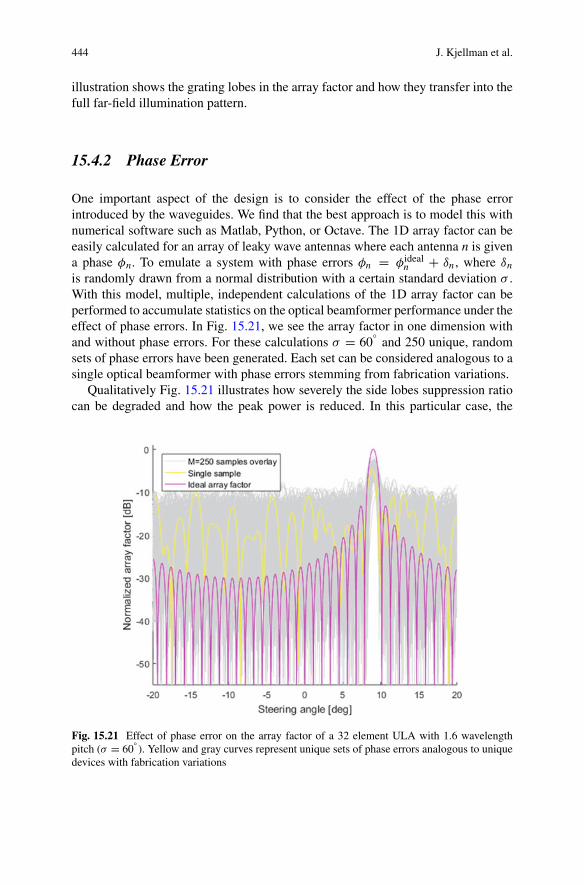
444 J. Kjellman et al.
illustration shows the grating lobes in the array factor and how they transfer into thefull far-field illumination pattern.
15.4.2 Phase Error
One important aspect of the design is to consider the effect of the phase errorintroduced by the waveguides. We find that the best approach is to model this withnumerical software such as Matlab, Python, or Octave. The 1D array factor can beeasily calculated for an array of leaky wave antennas where each antenna n is givena phase φn. To emulate a system with phase errors φn = φideal
n + δn, where δn
is randomly drawn from a normal distribution with a certain standard deviation σ .With this model, multiple, independent calculations of the 1D array factor can beperformed to accumulate statistics on the optical beamformer performance under theeffect of phase errors. In Fig. 15.21, we see the array factor in one dimension withand without phase errors. For these calculations σ = 60
◦and 250 unique, random
sets of phase errors have been generated. Each set can be considered analogous to asingle optical beamformer with phase errors stemming from fabrication variations.
Qualitatively Fig. 15.21 illustrates how severely the side lobes suppression ratiocan be degraded and how the peak power is reduced. In this particular case, the
Fig. 15.21 Effect of phase error on the array factor of a 32 element ULA with 1.6 wavelengthpitch (σ = 60
◦). Yellow and gray curves represent unique sets of phase errors analogous to unique
devices with fabrication variations
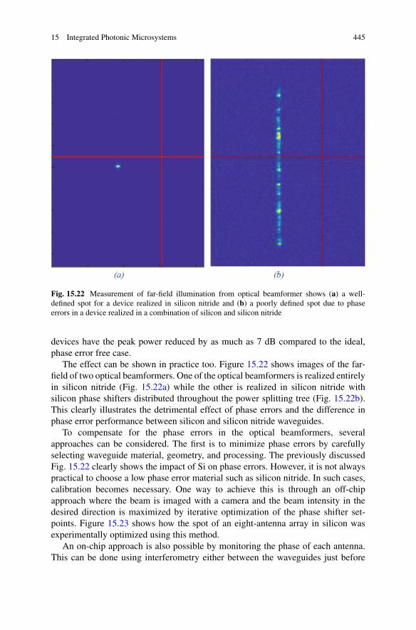
15 Integrated Photonic Microsystems 445
Fig. 15.22 Measurement of far-field illumination from optical beamformer shows (a) a well-defined spot for a device realized in silicon nitride and (b) a poorly defined spot due to phaseerrors in a device realized in a combination of silicon and silicon nitride
devices have the peak power reduced by as much as 7 dB compared to the ideal,phase error free case.
The effect can be shown in practice too. Figure 15.22 shows images of the far-field of two optical beamformers. One of the optical beamformers is realized entirelyin silicon nitride (Fig. 15.22a) while the other is realized in silicon nitride withsilicon phase shifters distributed throughout the power splitting tree (Fig. 15.22b).This clearly illustrates the detrimental effect of phase errors and the difference inphase error performance between silicon and silicon nitride waveguides.
To compensate for the phase errors in the optical beamformers, severalapproaches can be considered. The first is to minimize phase errors by carefullyselecting waveguide material, geometry, and processing. The previously discussedFig. 15.22 clearly shows the impact of Si on phase errors. However, it is not alwayspractical to choose a low phase error material such as silicon nitride. In such cases,calibration becomes necessary. One way to achieve this is through an off-chipapproach where the beam is imaged with a camera and the beam intensity in thedesired direction is maximized by iterative optimization of the phase shifter set-points. Figure 15.23 shows how the spot of an eight-antenna array in silicon wasexperimentally optimized using this method.
An on-chip approach is also possible by monitoring the phase of each antenna.This can be done using interferometry either between the waveguides just before
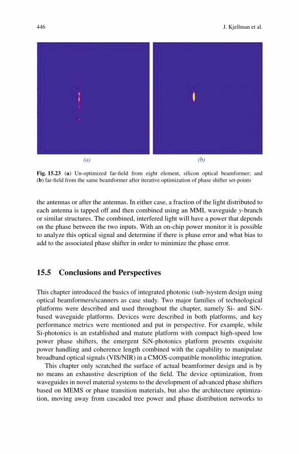
446 J. Kjellman et al.
Fig. 15.23 (a) Un-optimized far-field from eight element, silicon optical beamformer; and(b) far-field from the same beamformer after iterative optimization of phase shifter set-points
the antennas or after the antennas. In either case, a fraction of the light distributed toeach antenna is tapped off and then combined using an MMI, waveguide y-branchor similar structures. The combined, interfered light will have a power that dependson the phase between the two inputs. With an on-chip power monitor it is possibleto analyze this optical signal and determine if there is phase error and what bias toadd to the associated phase shifter in order to minimize the phase error.
15.5 Conclusions and Perspectives
This chapter introduced the basics of integrated photonic (sub-)system design usingoptical beamformers/scanners as case study. Two major families of technologicalplatforms were described and used throughout the chapter, namely Si- and SiN-based waveguide platforms. Devices were described in both platforms, and keyperformance metrics were mentioned and put in perspective. For example, whileSi-photonics is an established and mature platform with compact high-speed lowpower phase shifters, the emergent SiN-photonics platform presents exquisitepower handling and coherence length combined with the capability to manipulatebroadband optical signals (VIS/NIR) in a CMOS-compatible monolithic integration.
This chapter only scratched the surface of actual beamformer design and is byno means an exhaustive description of the field. The device optimization, fromwaveguides in novel material systems to the development of advanced phase shiftersbased on MEMS or phase transition materials, but also the architecture optimiza-tion, moving away from cascaded tree power and phase distribution networks to
15 Integrated Photonic Microsystems 447
alternatives like the switched Rotman lens approach are ongoing vibrant activitiesin the integrated photonics community that cannot be summarized in these shortpages. The enthused reader is encouraged to join the field and contribute to or useits development for novel applications in life sciences, industrial sensing, AR/VR,energy, automotive, etc.
References
1. P. Absil et al., Silicon photonics integrated circuits: a manufacturing platform for high density,low power optical I/O’s. Opt. Express 23(7), 9369–9378 (2015)
2. A. Subramanian et al., Low-loss singlemode PECVD silicon nitride photonic wire waveguidesfor 532–900 nm wavelength window fabricated within a CMOS pilot line. IEEE Photon. J.5(6), 2202809 (2013)
3. T. Shoji et al., Low loss mode size converter from 0.3 μm square Si wire waveguides tosinglemode fibres. Electron. Lett. 38(25), 1669–1670 (2002)
4. C. Alonso-Ramos et al., Efficient fiber-to-chip grating coupler for micrometric SOI ribwaveguides. Opt. Express 18(14), 15189–15200 (2010)
5. D. Vermeulen et al., Reflectionless grating couplers for Silicon-on-Insulator photonic inte-grated circuits. Opt. Express 20(20), 22278–22283 (2012)
6. M. Antelius, K.B. Gylfason, H. Sohlström, An apodized SOI waveguide-to-fiber surfacegrating coupler for single lithography silicon photonics. Opt. Express 19(4), 3592–3598 (2011)
7. Y. Wang et al., Focusing sub-wavelength grating couplers with low back reflections for rapidprototyping of silicon photonic circuits. Opt. Express 22(17), 20652–20662 (2014)
8. J.H. Song, X. Rottenberg, Low-back-reflection grating couplers using asymmetric gratingtrenches. IEEE Photon. Technol. Lett. 29(4), 389–392 (2017)
9. J.H. Song et al., Grating coupler design for reduced back-reflections. IEEE Photon. Technol.Lett. 30(2), 217–220 (2018)
10. C.R. Doerr et al., Wide bandwidth silicon nitride grating coupler. IEEE Photon. Technol. Lett.22(19), 1461–1463 (2010)
11. J.H. Song et al., Grating devices on a silicon nitride technology platform for visible lightapplications. OSA Continuum 2, 1155–1165 (2019)
12. ANSYS HFSS. [Online]. https://www.ansys.com/products/electronics/ansys-hfss. Accessed17 Feb 2019
13. R. Adar et al., Phase coherence of optical waveguides. OSA (1993)14. D. Bristow et al., Two-photon absorption and Kerr coefficients of silicon for 850–2200nm.
Appl. Phys. Lett. 90, 191104 (2007)15. N. Hosseini et al., Stress-optic modulator in TriPleX platform using a piezoelectric lead
zirconate titanate (PZT) thin film. Opt. Express 23, 14018–14026 (2015)16. A. Koen et al., Nanophotonic Pockels modulators on a silicon nitride platform. Nat. Commun.
9, 3444 (2018)
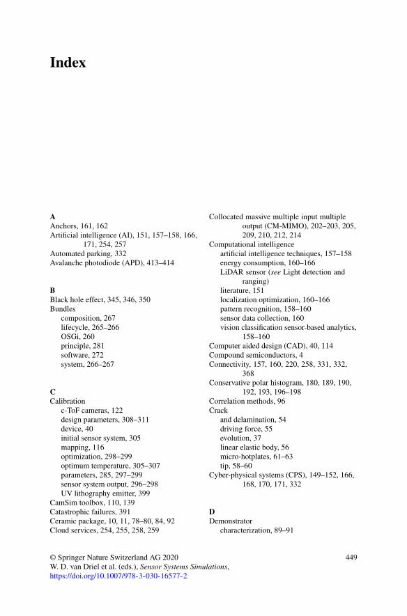
Index
AAnchors, 161, 162Artificial intelligence (AI), 151, 157–158, 166,
171, 254, 257Automated parking, 332Avalanche photodiode (APD), 413–414
BBlack hole effect, 345, 346, 350Bundles
composition, 267lifecycle, 265–266OSGi, 260principle, 281software, 272system, 266–267
CCalibration
c-ToF cameras, 122design parameters, 308–311device, 40initial sensor system, 305mapping, 116optimization, 298–299optimum temperature, 305–307parameters, 285, 297–299sensor system output, 296–298UV lithography emitter, 399
CamSim toolbox, 110, 139Catastrophic failures, 391Ceramic package, 10, 11, 78–80, 84, 92Cloud services, 254, 255, 258, 259
Collocated massive multiple input multipleoutput (CM-MIMO), 202–203, 205,209, 210, 212, 214
Computational intelligenceartificial intelligence techniques, 157–158energy consumption, 160–166LiDAR sensor (see Light detection and
ranging)literature, 151localization optimization, 160–166pattern recognition, 158–160sensor data collection, 160vision classification sensor-based analytics,
158–160Computer aided design (CAD), 40, 114Compound semiconductors, 4Connectivity, 157, 160, 220, 258, 331, 332,
368Conservative polar histogram, 180, 189, 190,
192, 193, 196–198Correlation methods, 96Crack
and delamination, 54driving force, 55evolution, 37linear elastic body, 56micro-hotplates, 61–63tip, 58–60
Cyber-physical systems (CPS), 149–152, 166,168, 170, 171, 332
DDemonstrator
characterization, 89–91
© Springer Nature Switzerland AG 2020W. D. van Driel et al. (eds.), Sensor Systems Simulations,https://doi.org/10.1007/978-3-030-16577-2
449
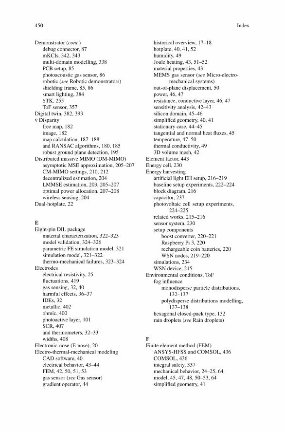
450 Index
Demonstrator (cont.)debug connector, 87mKCIs, 342, 343multi-domain modelling, 338PCB setup, 85photoacoustic gas sensor, 86robotic (see Robotic demonstrators)shielding frame, 85, 86smart lighting, 384STK, 255ToF sensor, 357
Digital twin, 382, 393v Disparity
free map, 182image, 182map calculation, 187–188and RANSAC algorithms, 180, 185robust ground plane detection, 195
Distributed massive MIMO (DM-MIMO)asymptotic MSE approximation, 205–207CM-MIMO settings, 210, 212decentralized estimation, 204LMMSE estimation, 203, 205–207optimal power allocation, 207–208wireless sensing, 204
Dual-hotplate, 22
EEight-pin DIL package
material characterization, 322–323model validation, 324–326parametric FE simulation model, 321simulation model, 321–322thermo-mechanical failures, 323–324
Electrodeselectrical resistivity, 25fluctuations, 419gas sensing, 32, 40harmful effects, 36–37IDEs, 32metallic, 402ohmic, 400photoactive layer, 101SCR, 407and thermometers, 32–33widths, 408
Electronic-nose (E-nose), 20Electro-thermal-mechanical modeling
CAD software, 40electrical behavior, 43–44FEM, 42, 50, 51, 53gas sensor (see Gas sensor)gradient operator, 44
historical overview, 17–18hotplate, 40, 41, 52humidity, 49Joule heating, 43, 51–52material properties, 43MEMS gas sensor (see Micro-electro-
mechanical systems)out-of-plane displacement, 50power, 46, 47resistance, conductive layer, 46, 47sensitivity analysis, 42–43silicon domain, 45–46simplified geometry, 40, 41stationary case, 44–45tangential and normal heat fluxes, 45temperature, 47–50thermal conductivity, 493D volume mesh, 42
Element factor, 443Energy cell, 230Energy harvesting
artificial light EH setup, 216–219baseline setup experiments, 222–224block diagram, 216capacitor, 237photovoltaic cell setup experiments,
224–225related works, 215–216sensor system, 230setup components
boost converter, 220–221Raspberry Pi 3, 220rechargeable coin batteries, 220WSN nodes, 219–220
simulations, 234WSN device, 215
Environmental conditions, ToFfog influence
monodisperse particle distributions,132–137
polydisperse distributions modelling,137–138
hexagonal closed-pack type, 132rain droplets (see Rain droplets)
FFinite element method (FEM)
ANSYS-HFSS and COMSOL, 436COMSOL, 436integral safety, 337mechanical behavior, 24–25, 64model, 45, 47, 48, 50–53, 64simplified geometry, 41
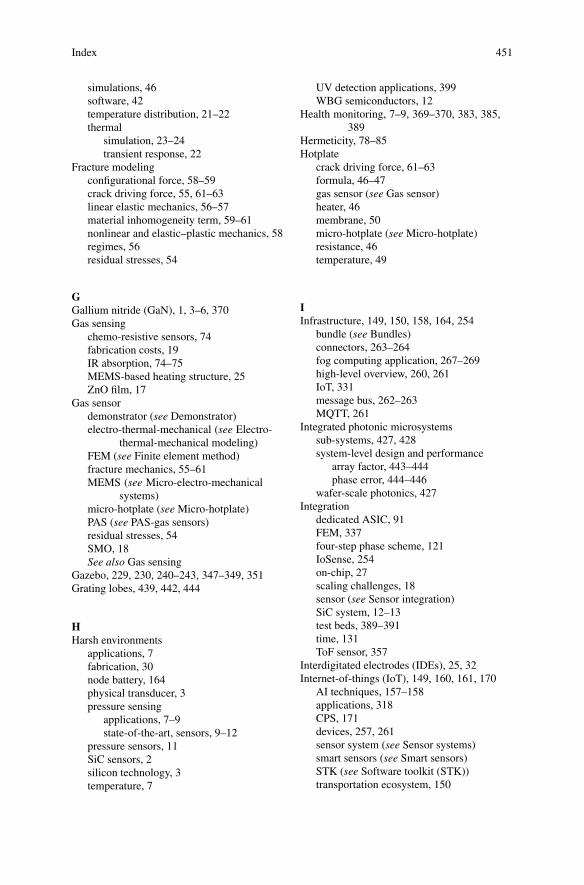
Index 451
simulations, 46software, 42temperature distribution, 21–22thermal
simulation, 23–24transient response, 22
Fracture modelingconfigurational force, 58–59crack driving force, 55, 61–63linear elastic mechanics, 56–57material inhomogeneity term, 59–61nonlinear and elastic–plastic mechanics, 58regimes, 56residual stresses, 54
GGallium nitride (GaN), 1, 3–6, 370Gas sensing
chemo-resistive sensors, 74fabrication costs, 19IR absorption, 74–75MEMS-based heating structure, 25ZnO film, 17
Gas sensordemonstrator (see Demonstrator)electro-thermal-mechanical (see Electro-
thermal-mechanical modeling)FEM (see Finite element method)fracture mechanics, 55–61MEMS (see Micro-electro-mechanical
systems)micro-hotplate (see Micro-hotplate)PAS (see PAS-gas sensors)residual stresses, 54SMO, 18See also Gas sensing
Gazebo, 229, 230, 240–243, 347–349, 351Grating lobes, 439, 442, 444
HHarsh environments
applications, 7fabrication, 30node battery, 164physical transducer, 3pressure sensing
applications, 7–9state-of-the-art, sensors, 9–12
pressure sensors, 11SiC sensors, 2silicon technology, 3temperature, 7
UV detection applications, 399WBG semiconductors, 12
Health monitoring, 7–9, 369–370, 383, 385,389
Hermeticity, 78–85Hotplate
crack driving force, 61–63formula, 46–47gas sensor (see Gas sensor)heater, 46membrane, 50micro-hotplate (see Micro-hotplate)resistance, 46temperature, 49
IInfrastructure, 149, 150, 158, 164, 254
bundle (see Bundles)connectors, 263–264fog computing application, 267–269high-level overview, 260, 261IoT, 331message bus, 262–263MQTT, 261
Integrated photonic microsystemssub-systems, 427, 428system-level design and performance
array factor, 443–444phase error, 444–446
wafer-scale photonics, 427Integration
dedicated ASIC, 91FEM, 337four-step phase scheme, 121IoSense, 254on-chip, 27scaling challenges, 18sensor (see Sensor integration)SiC system, 12–13test beds, 389–391time, 131ToF sensor, 357
Interdigitated electrodes (IDEs), 25, 32Internet-of-things (IoT), 149, 160, 161, 170
AI techniques, 157–158applications, 318CPS, 171devices, 257, 261sensor system (see Sensor systems)smart sensors (see Smart sensors)STK (see Software toolkit (STK))transportation ecosystem, 150
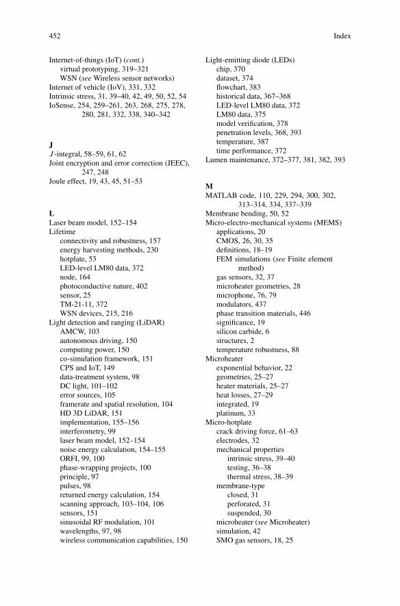
452 Index
Internet-of-things (IoT) (cont.)virtual prototyping, 319–321WSN (see Wireless sensor networks)
Internet of vehicle (IoV), 331, 332Intrinsic stress, 31, 39–40, 42, 49, 50, 52, 54IoSense, 254, 259–261, 263, 268, 275, 278,
280, 281, 332, 338, 340–342
JJ -integral, 58–59, 61, 62Joint encryption and error correction (JEEC),
247, 248Joule effect, 19, 43, 45, 51–53
LLaser beam model, 152–154Lifetime
connectivity and robustness, 157energy harvesting methods, 230hotplate, 53LED-level LM80 data, 372node, 164photoconductive nature, 402sensor, 25TM-21-11, 372WSN devices, 215, 216
Light detection and ranging (LiDAR)AMCW, 103autonomous driving, 150computing power, 150co-simulation framework, 151CPS and IoT, 149data-treatment system, 98DC light, 101–102error sources, 105framerate and spatial resolution, 104HD 3D LiDAR, 151implementation, 155–156interferometry, 99laser beam model, 152–154noise energy calculation, 154–155ORFI, 99, 100phase-wrapping projects, 100principle, 97pulses, 98returned energy calculation, 154scanning approach, 103–104, 106sensors, 151sinusoidal RF modulation, 101wavelengths, 97, 98wireless communication capabilities, 150
Light-emitting diode (LEDs)chip, 370dataset, 374flowchart, 383historical data, 367–368LED-level LM80 data, 372LM80 data, 375model verification, 378penetration levels, 368, 393temperature, 387time performance, 372
Lumen maintenance, 372–377, 381, 382, 393
MMATLAB code, 110, 229, 294, 300, 302,
313–314, 334, 337–339Membrane bending, 50, 52Micro-electro-mechanical systems (MEMS)
applications, 20CMOS, 26, 30, 35definitions, 18–19FEM simulations (see Finite element
method)gas sensors, 32, 37microheater geometries, 28microphone, 76, 79modulators, 437phase transition materials, 446significance, 19silicon carbide, 6structures, 2temperature robustness, 88
Microheaterexponential behavior, 22geometries, 25–27heater materials, 25–27heat losses, 27–29integrated, 19platinum, 33
Micro-hotplatecrack driving force, 61–63electrodes, 32mechanical properties
intrinsic stress, 39–40testing, 36–38thermal stress, 38–39
membrane-typeclosed, 31perforated, 31suspended, 30
microheater (see Microheater)simulation, 42SMO gas sensors, 18, 25

Index 453
thermal propertiescharacterization, 34modeling, 34–36
thermometers, 32–33Mie-scattering, 132, 133, 137, 139Model based design
optimized sensors, 227secured power aware smart sensor, 228smart sensors (see Smart sensors)
Model verification, 377–378More than Moore (MtM), 1, 2
NNon-resonant system, 74
OObstacle recognition, 151, 166, 168, 171,
189–192Offset error, 297Opaque, 421Optical beamformer
in-and out-couplers, 428–432leaky wave antenna, 438–441phase shifters and modulators, 437–438power splitters, 435–437waveguides, 432–435
PPackage development
bonded pressure, 84ceramic, 78DIL, 319eight-pin DIL (see Eight-pin DIL package)LED, 373PoP, 318SiP, 12and system requirements, 77
Parking assistance scenario, ToFalgorithms
camera obstacle detection, 362egomotion estimation, vehicle, 359–361time-to-collision reasoning, 362–364vehicle trajectory prediction, 361, 362
simulation elementsscenarios configuration, 359sensor, 355–358vehicle/demonstrator, 354, 355
PAS-gas sensorsautomotive
applications, 88requirements, 88–89
IR sensor, 91leak rate model, 80reliability, 89
Phonons, 35, 36Photoacoustic effect
absorption band, 75ceramic package, 92demonstrator, 86gas sensor (see Gas sensor)sensor concept, 76–77
Photoconductor, 397, 400–402, 422Photodetection
bandwidth, 423dynamic range, 423linearity, 423minimum detectable optical power,
419–420OPF, 400optical absorption coefficient, 421PC mode, 416–417response time and persistent
photoconductivity, 422–423SNR, 417–419spectral response, 417UV-to-visible ratio, 397, 417
Photovoltaic (PV) cell, 202, 215–218,220–225, 414–415
PN-junction photodiodesbuilt-in voltage, 405charge carriers, 411illustrations, 411light absorption, 413photodiode, 4106H-SiC UV, 412SCR, 412
Power allocationCM-MIMO, 202–203DM-MIMO system, 205–214EE, 202multiple distributed access points, 203numerical results, 209–214system model, 203–205total transmitted power, 214WSN, 201, 202, 204
Power dissipation, 43, 46, 47, 64Primitive cell, 5Prognostics, 369, 370, 373Prototypes
development cycle, 21diagnostic module, 389input voltages, 232model-based design approach, 227research, 227
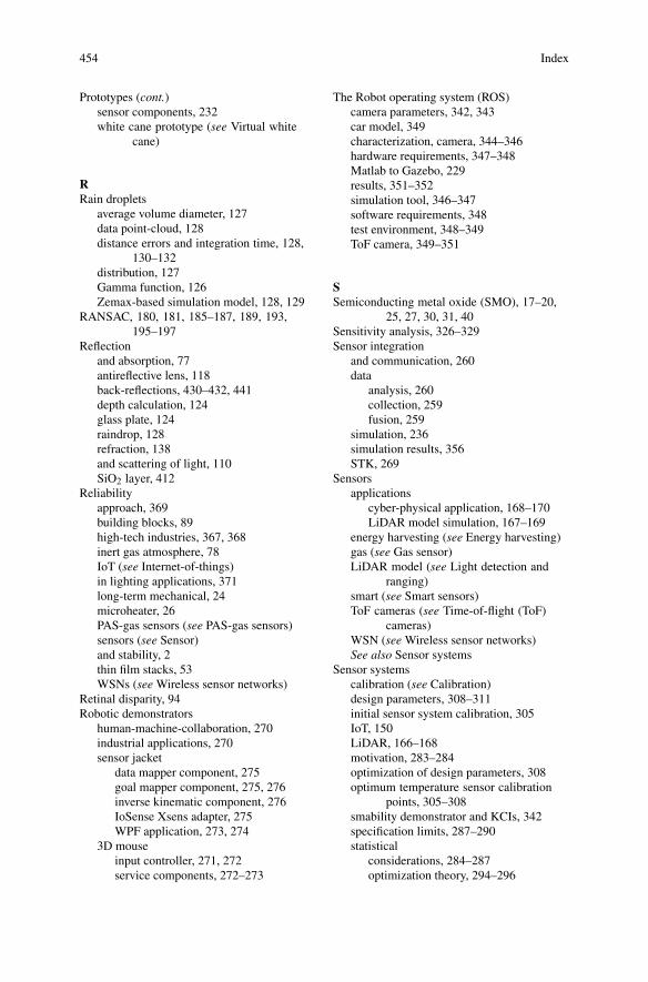
454 Index
Prototypes (cont.)sensor components, 232white cane prototype (see Virtual white
cane)
RRain droplets
average volume diameter, 127data point-cloud, 128distance errors and integration time, 128,
130–132distribution, 127Gamma function, 126Zemax-based simulation model, 128, 129
RANSAC, 180, 181, 185–187, 189, 193,195–197
Reflectionand absorption, 77antireflective lens, 118back-reflections, 430–432, 441depth calculation, 124glass plate, 124raindrop, 128refraction, 138and scattering of light, 110SiO2 layer, 412
Reliabilityapproach, 369building blocks, 89high-tech industries, 367, 368inert gas atmosphere, 78IoT (see Internet-of-things)in lighting applications, 371long-term mechanical, 24microheater, 26PAS-gas sensors (see PAS-gas sensors)sensors (see Sensor)and stability, 2thin film stacks, 53WSNs (see Wireless sensor networks)
Retinal disparity, 94Robotic demonstrators
human-machine-collaboration, 270industrial applications, 270sensor jacket
data mapper component, 275goal mapper component, 275, 276inverse kinematic component, 276IoSense Xsens adapter, 275WPF application, 273, 274
3D mouseinput controller, 271, 272service components, 272–273
The Robot operating system (ROS)camera parameters, 342, 343car model, 349characterization, camera, 344–346hardware requirements, 347–348Matlab to Gazebo, 229results, 351–352simulation tool, 346–347software requirements, 348test environment, 348–349ToF camera, 349–351
SSemiconducting metal oxide (SMO), 17–20,
25, 27, 30, 31, 40Sensitivity analysis, 326–329Sensor integration
and communication, 260data
analysis, 260collection, 259fusion, 259
simulation, 236simulation results, 356STK, 269
Sensorsapplications
cyber-physical application, 168–170LiDAR model simulation, 167–169
energy harvesting (see Energy harvesting)gas (see Gas sensor)LiDAR model (see Light detection and
ranging)smart (see Smart sensors)ToF cameras (see Time-of-flight (ToF)
cameras)WSN (see Wireless sensor networks)See also Sensor systems
Sensor systemscalibration (see Calibration)design parameters, 308–311initial sensor system calibration, 305IoT, 150LiDAR, 166–168motivation, 283–284optimization of design parameters, 308optimum temperature sensor calibration
points, 305–308smability demonstrator and KCIs, 342specification limits, 287–290statistical
considerations, 284–287optimization theory, 294–296
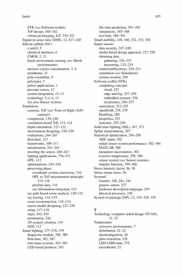
Index 455
STK (see Software toolkit)ToF design, 340–342virtual prototyping, IoT, 319–321
Signal-to-noise ratio (SNR), 12, 417–420Silicon carbide (SiC)
chemical inertness, 6CMOS, 2, 13harsh environment sensing (see Harsh
environments)intrinsic carrier concentration, 3, 4membrane, 31poly-crystalline, 9polytypes, 5power applications, 1pressure sensor, 13system integration, 12–13technology, 2–4, 6, 13See also Sensor systems
Simulationcameras, ToF (see Time-of-flight (ToF)
cameras)comparison, 138–140correlation-based ToF, 113–114depth calculation, 121–122environment designing, 238–239evaluations, 244–247flowchart, 113frameworks, 109–111initialization, 241–242inserting the sensor, 240–241lighting applications, 370–371OPL, 112optimizations, 243–244processing phase
coordinate system conversion, 116OPL to ToF measurement principle,
115–116pixelate data, 116ray information extraction, 115
ray path-based scene analysis, 120–121ray-tracing, 114–115scene reconstruction, 118–119sensor model designing, 237–238setup, 117–118steps, 242–243termination, 2433D scenery creation, 114ZOS, 112
Smart lighting, 277–278, 379diagnostic module, 388, 389flowchart, 382, 383four main systems, 383–385LED-based products, 393
life time prediction, 391–392simulations, 385–388test beds, 389–391
Smart mobility, 149, 160, 332, 333, 354Smart sensors
data security, 247–249model-based design approach, 227, 228obtaining data
gathering, 236–237measuring, 232–235
related publications, 229–231simulation (see Simulation)system security, 249
Software toolkit (STK)computing concepts
cloud, 257edge and fog, 257–259embedded systems, 256on-premise, 256–257
motivation, 253–255openHAB, 278, 279ParaDrop, 280properties, 253structure, 255–256
Solid state lighting (SSL), 367, 371Spline interpolations, 297Statistical optimization, 294–296
ADC-input, 302initial sensor system performance, 302–304MATLAB, 300parameter uncertainties, 301resistive temperature, 299, 300sensor system (see Sensor systems)transfer-function, 299–300
Stress intensity factor, 56, 58Stress–strain curve, 58SystemC
Gazebo, 240, 241, 243generic sensor, 237hardware description language, 229physical processes, 230
System-in-package (SiP), 12, 318–320, 329
TTechnology computer aided design (TCAD),
21, 23Temperature
corrosive environments, 7distribution, 21–22electromigration, 26glass transition, 328LED LM80 data, 375microheater, 32
α and β, 5
456 Index
Temperature (cont.)sensors, 385silicon technology, 2–4substrate-based implementation, 10TaAl, 27test bed, 390thermal stress, 31uniformity, 21
Thermal stress, 25, 30, 31, 38–39, 49, 51, 52,54, 437
Thermo-mechanics, 24, 43, 65–66, 80, 318,322–324, 329
Thermometers, 32–34Time-of-flight (ToF) cameras
comparison, 138–139contributions, 180depth
calculation, 121–122perception technology, 179
disparity map, 182multipath interference, 106–109obstacle warning, 180optical
range detection, 93–97round-trip time measurement methods
(see Light detection and ranging)sensors system (see Sensors system)simulation
frameworks, 109–111procedure (see Simulation)ROS (see The Robot operating system
(ROS))time-gated, 123transparent objects
environment (see Environmentalconditions, ToF)
glass window, 124–126virtual white cane (see Virtual white cane)
Toolkit, see Software toolkit (STK)
UUltraviolet (UV)
applications, 399electromagnetic spectrum, 397, 398MSM
contact current mechanism, 409–410Schottky Photodetector, 402–408
photoconductor, 400–402photodetection, 397–398pn-junction photodiode (see PN-junction
photodiodes)state of the art, 399–400
Uncertainty, 379–382
Uncertainty propagationcorrelated parameters, 290–291Gaussian probability distributions,
291–294, 310principle, 293
Uncertainty toolbox, 294, 299, 302, 304, 305,310, 312–314
VVirtual prototyping, 151, 318–321, 324, 329Virtual white cane
acoustic warning, 193cluttered scenes, 193, 194v disparity, 186–188, 194, 195floor segmentation results, 193, 194flow of operations, 185ground detection module, 185–186Lenovo Phab 2 Pro, 184obstacle detection, 189–192performance data, 196RANSAC, 189, 193requirements, 183tilt angle, 184–185visualized conservative polar histogram,
196, 197
WWaveguides, 429–435, 437–440, 446Wide bandgap (WBG), 1, 4–6, 398, 402, 412,
435compound semiconductors, 4counterpart materials, 3in harsh environments, 12physical properties, 5–6polytypes, 5power applications, 1semiconductors, 402
Wireless sensor networks (WSNs)APs, 201–202artificial light EH, 202battery-powered, 201energy consumption, 157harvesting artificial light indoors (see
Energy harvesting)IoT (see Internet-of-things)localization, 162, 164nodes, 219–220, 224power allocation (see Power allocation)reliability, 161self-configuration algorithm, 166sensor nodes, 164


![Cornelia POPA-GORJANU, Skylitzès şi Genesios despre împăratul Theophylos [Skylitzès and Genesios on Emperor Theophylos]](https://img.pdfslide.net/doc/110x75/635da9911b1c1ace2609262f/cornelia-popa-gorjanu-skylitzes-si-genesios-despre-imparatul-theophylos-skylitzes.jpg)


![[Free-scores com] schumann-robert-kinderscenen-1458](https://img.pdfslide.net/doc/110x75/6312f1f55cba183dbf06dffd/free-scores-com-schumann-robert-kinderscenen-1458.jpg)


