Embed Size (px)
Citation preview
WIRELESS ENGINEER
Vol. 32 DECEMBER 1955 No. 12
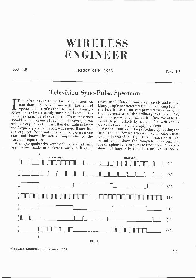
Television Sync -Pulse Spectrum JT is often easier to perform calculations on
non -sinusoidal waveforms with the aid of operational calculus than to use the Fourier -
series method with steady-state a.c. theory. It is not surprising, therefore, that the Fourier method should be falling out of favour. However, it can still be very helpful. It is often desirable to know the frequency spectrum of a wave even if one does not employ it for actual calculation and even if one does not know the actual amplitudes of the various frequencies.
A simple qualitative approach, or several such íLpproaches made in different ways, \vill often
0
o
o
o
o
o
A
1 EVEN FRAMES
A
\VII2ELb;sS ENGINEER, 111iCEmBER 1955
reveal useful information very quickly and easil\ .
Many people are deterred f-om attempting to find the Fourier series for complicated waveforms by the laboriousness of the ordinary methods. We want to point out that it is often possible to avoid these methods by using a few well-known series and adding or multiplying them.
We shall illustrate the procedure by finding the series for the British television sync -pulse wave- form, illustrated at Fig. 1(a). Space does not permit us to draw the complete waveform for one complete cycle at picture frequency . We have shown 15 lines only and there are 390 others in
ODD FRAMES
Fig. 1.
(a)
(b)
(c )
313
the central gap; they are, however, identical with the initial lines on the left.
The first step is to consider how one could generate such a waveform. One would obviously start by generating a simple line -frequency pulse waveform like (b). This agrees with (a) every- where except during the frame pulses. The obvious next step is to suppress the line pulses during the frame -pulse periods and one could do this in a gating stage. One could, for instance, use a multi -electrode valve with the line pulses applied to one grid and frame -frequency pulses applied to another to cut it off during these pulses. Practically, there would be difficulties with such a simple gating circuit, but that sloes not affect our general argument. The required trame - frequency waveform would be like (c) and the resulting output would be like (f), a line -frequency pulse waveform with certain pulses. suppressed.
In Fig. 1 we have shown the pulses as being of unit amplitude; the signal is either zero or unity. \Vaveform (f) can thus be produced by multiplying together waveforms (b) and (c). The Fourier series for (f) can thus be obtained by multiplying together the individual Fourier series for (b) and (c) .
Now one cycle of wati eforn) (b) is a simple rectangular wave like Fig. 2.and it is well known that its Fourier series is
S = ao a sin nu)/ b,z eos . .Had (1)
where w = 27rf = 27r/7' and a is integral; the values of the coefficients ao, a and b depend upon the value of T/T, the fractional pulse width and the order a of the harmonic (Fig. 2).
rT-1
' 1-1_ o. la-T Fig. 2.
It should be noted that all the waves in Fig. 1
have a transition at AA. A single cycle of any wave is therefore like Fig. 2 or its inverse and this must be taken into account in evaluating the coefficients ao, an and b11. \Ve shall not attempt this evaluation here.
\Ve shall designate the various series by the letter S with a subscript letter according to the fundamental recurrence frequency. The series for (b) is thus S, and is equation (1) with
= wl = 27r times the line frequency and the appropriate coefficients.
\Vaveform (c) is the inverse of waveform (e).
Now the series for (e) is Sf and is clearly identical with (1) with w = w f = 27r times the frame frequency and the appropriate coefficients. It is
clear, too, that (c) is 1 - SI and so the series for
waveform (f) is
Sc(1 - 51)
;314
\Ve have now to produce a waveform to fill the gaps in (f). By arguing on the same lines as before, we can clearly do this by generating (d)
of twice the line frequency and gating it with (e) to produce (g). \Ve then get (a) by adding (f) and (g).
The basic series for (d) is (1) with w = 2wj
= 27r times twice the line frequency. However, (d) is inverted compared with the wave which (1)
represents so the series is
1 - S2/ The gating waveform is Sf and so the series corresponding to (g) is
S1(1 - 521)
The complete series representing (a) is thus
St(1 - Sf) -r Sf(1 - S21)
= S1 + St -S f(S1 + S21)
\Ve can at once see the form of the spectrum of (a). First of all, there is the frame frequency of 50 c/s and all its harmonics. Then there is
the line frequency of 10.125 kc/s and all its harmonics.
The term S1 + S21 represents line frequency and all harmonics plus twice line frequency and all harmonics. However, S21 and its harmonics coincide with the even harmonics of line frequency, so that S¡ -{ 521 represents Sr with modified amplitudes of even harmonics. The spectrum of
Si -F- S21 is thus the same as that of S/. Now Sf(.S1 + 521) is the product of a series
in Ulf with a series in (Di and produces terms like
sin w11 sin wit. These terms can be split into sum and difference form and so the full spectrum of Sf(S, + S2i) is of the form ufi ± rf. f. In other words, the line frequency and its harmonics are all modulated by the frame frequency and its harmonics.
The complete frequency spectrum thus com- prises the frame frequency and all its harmonics, plus the line frequency and all its harmonics, plus sidebands (of frame frequency and all its harmonics) to the line frequency and all its harmonics. Thus,
50, 10,125 ± 50, 20,250 f 50, 30,375 ± 50, etc.
Since 10,125 is a multiple of 50/2, all the side - bands associated with the even harmonics of
line frequency and the even harmonics themselves coincide with harmonics of frame frequency. All the sidebands associated with odd harmonics, the odd harmonics themselves and the fundamental of line frequency fall mid -way between the harmonics of frame frequency and thus 25 c/s from them.
100, 150, 200, 250, etc. c/s 100, 150, 200, 250, etc. c/s 100, 150, 200, 250, etc. c/s 100, 150, 200, 250, etc. c/s
WIRELESS ENGINEER, 1)Ecr:mHHER 15)55
It is thus possible for a component frequency of 25 cis to appear, although the lowest funda- mental frequency is 50 c/s ! It appears as a sideband of the line frequency. Harmonic number 202 of 50 c s is 10,100 c/s and produces sidebands of 10,125 + 10,100 c/s to the line frequency fundamental. The lower sideband is 25 c/s.
We can say, therefore, that the complete frequency spectrum may comprise all integral multiples of 25 c/s.
Since we have not investigated the amplitudes of the terms, we cannot say anything about their relative importance. Since some frequencies are produced in several different ways, there is a possibility of one method of production cancelling another and so some frequencies of the spectrum may be missing.
The amplitudes of the terms in the basic series (1) fall off fairly rapidly with order of harmonic. The predominating terms in the complete series are thus likely to be those involving fundamentals of low -order harmonics in simple combination. The main terms are thus likely to be the frame frequency and its first few harmonics, the line frequency and its first few harmonics, and the low -order sidebands attached to these.
The presence of the 25-c/s component in the spectrum may seem a little odd and, because its production involves the 202nd harmonic of frame frequency, one is tempted to consider it as negligibly small. However, one could have predicted its presence by inspection of Fig. 1, for the waveform repeats itself precisely only every two frames. At the beginning and end of the frame pulses there are differences between odd and even frames brought about by the non - integral relation of line and frame frequencies.
When the frame pulses are separated from the line pulses before they are applied to synchronize the frame time -base, some methods result in there being a difference of waveform between odd and even frames at the end of the pulses. Patchett! has shown that it is this which accounts for many, if not most, difficulties in obtaining good inter-
lacing. These differences necessarily imply the presence of a 25-c/s component.
It is easy to show that two successive frame scans must be alike within 1 part in 4,000 if interlacing is not to be appreciably affected. An error of 50 µsec in the timing will destroy the interlace and, as the frame period is 20 msec, this is an error of 1 part in 400. The 25-c/s component of the sync -pulse waveform thus does not need to be very large to affect matters.
The waveform of Fig. 1(a) is not, of course, applied in this form to the time -base for syn- chronizing. It is always operated on in some way first. If an integrator is used its effect will be to emphasize the relative amplitude of the 25-c/s component.
There is also a form of flywheel synchronizing for a line time -base in which the complete sync - pulse waveform is applied to a resonant circuit which is supposed to select only the line -frequency component and provide a sine -wave output. By the selectivity of the circuit, noise and interference are substantially removed and the sine wave is used, after suitable treatment, to control the time -base.
This circuit has been analysed on a pulse - response basis2 and it has been shown that, unless the resonant circuit is extremely selective, the output wave is seriously affected by the frame pulses. This seems rather surprising at first, because one tends to think loosely of the line pulses only, and that the selectivity problem is only to separate the fundamental from the second and higher harmonics, which is a fairly easy matter.
When we think of the true spectrum, however, we can see right away that the sidebands of frame frequency and its harmonics will have a profound influence. To extract a pure sine wave, the circuit must be selective enough to pass - 10,125 c/s while excluding frequencies 50 c/s higher and lower! W.T.C.
REFERENCES 'G. N. Patchett, "Faulty Interlacing", !tireless World, July and
August 1952, pp. 250 and 315. P. A. Neeteson, "Television Receiver Design", Monograph 2.
"Flywheel Synchronization of Saw -Tooth Generators". (Philips' 'technical Library, cleaver Ilume Press.)
WIRELESS ENGINEER, DIiC1i?II{I'.R 1955 315
11
RADIATION CHARACTERISTICS OF AXIAL SLOTS ON A CONDUCTING
CYLINDER By J. R. Wait, M.A.Sc., Ph.D.
(Radio Physics Laboratory, Defence Research Board, Ottawa, Ontario, Canada)
SUMMARY.-An extensive set of radiation patterns is presented for a narrow axial slot on a circular conducting cylinder of infinite length with a circumference up to 21 wavelengths. The results are also applicable to arrays of axial slots with an arbitrary distribution of transverse voltage. The effect of finite slot width is discussed and the external conductance of the slot is also considered.
Introduction THE slotted cylinder aerial has been discussed
in the literature quite extensively in the last decadel-7. In its simplest form it
consists of a narrow axial slot of rectangular shape cut in the wall of a hollow metal cylin ler. The slot is fed either by a transmission line inside the cylinder or by a waveguide. For most of the early applications the diameter of the cylinder was small compared to a wavelength and the radiation pattern is essentially omnidirectional in the equatorial plane. Sinclair3 has shown that for an axial s_ot the pattern becomes more direc- tive as the diameter of the cylinder is increased. Further computed curves of radiation patterns have been published by Silver and Saunders7 for slotted -cylinders whose circumferences are 0.8 and 2.5 wavelengths and by Bailing for circum- ferences of 8 and 12 wavelengths.
It is the purpose of this paper to present rather extensive calculations of radiation patterns of an axial slot on a circular cylinder with a circumference ranging from 0.1 to 21 wavelengths. It is shown that the results are also applicable to arrays of axial slots on the surface of the cylinder.
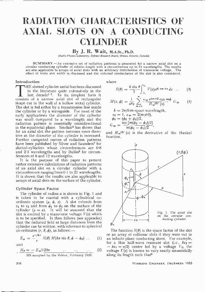
Cylinder Space Factor The cylinder of radius a is shown in Fig. 1 and
is taken to be coaxial with a cylindrical co- ordinate system (p, , z). A slot extends from z1 to z2 and from 01 to 02 on the surface of the cylinder (p = a). It will be assumed that the slot is excited by a transverse voltage V(z) which is to be specified. It then follows (see appendix) that the radiated field at large distances from the cylinder can be written, with reference to spherical co-ordinates (r, 0,56), as follows:-
e5 _ - --S(0) 117(ka sin B, - (4) . .
r' (1)
and Ho = - E6/1 207r . . . . . . (2)
316
MS accepted by the Editor, February 1955
where
= k sin B I'Z- COS '90 dz
z, CO
(3)
L1(x, (I)) = E,tt ei"1n12 cos rn0 (4) 1.
m= 77-,x2x Hni(2), (T)
k = 27r/free-space wavelength, EU = 1, E = 2(rn0),
= s(in2
+ ¢1)/2, m(42 - 01)/23 Gm = rn(02 - 01)/2
and H,12)' (x) is the derivative of the Hankel function.
(r,(9,p)
Fig. 1. The axial slot on the circular con-
ducting cylinder.
(Po
The function S(0) is the space factor of the slot or an array of collinear slots if they were cut in an infinite plane conducting sheet. For example, for a thin half -wave resonant slot (i.e., kz2 = - kz1 = 7r/2) centre fed by a voltage Vo, the voltage V(z) is known to vary nearly sinusoidally along its length such that9
WIRELESS ENGINEER, DECEMBER 1955
V(z) Vo sin (7r/2-itIz¡) and therefore, as is well known,
7r cos cos B
S(0) = I 0 '- sin O
For slots of arbitrary length the functional form of V(z) is not usually sinusoidal and depends on the method of excitation. For present purposes it is not necessary to specify V(z).
0'28
0'26
024
0.22
IM/ 020
0'18
0 16
0 14
.. (5)
rT \ IrJ2
` =01
0.120° 120°
20° 40° 60° 80° 1100° 120°
AZIMUTH
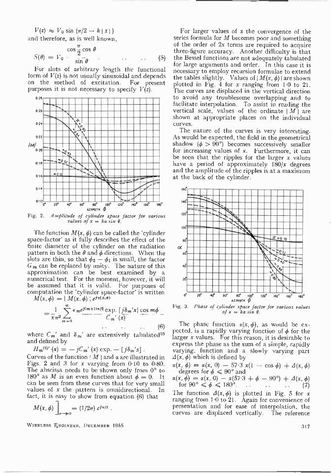
Fig. 2. A inplitude of cylinder space facto values of x = ha sill 8.
i 140' 160° 180°
for various
The function M(x, 0) can be called the 'cylinder space -factor' as it fully describes the effect of the finite diameter of the cylinder on the radiation pattern in both the O and 0 directions. When the slots are thin, so that ¢2 -
1 is small, the factor
G m can be replaced by unity. The nature of this approximation can be best examined by a numerical test. For the moment, however, it will be assumed that it is valid. For purposes of computation the 'cylinder space -factor' is written
M(x, = I M(x, (k)
I e'=tx,m)
1 e,neJlm+])n12 [ Om' xi cos nt0 x7r2 L Cm' (x)
0
.. (6)
where C,' and 8,18' are extensively tabulated]° and defined by
1j7l21' (x) = - jCm' (x) exp. - [ j8t'x] .
Curves of the function I M I and a are illustrated in Figs. 2 and 3 for x varying from 0.10 to 0.80. The abscissa needs to be shown only from 0° to 180° as M is an even function about 0 = 0. It can he seen from these curves that for very small values of x the pattern is omnidirectional. In fact, it is easy to show from equation (6) that
M (x, 0) ] = (1 /27) eJ l2
WIRELESS ENGINEER, DECEMBER 1955
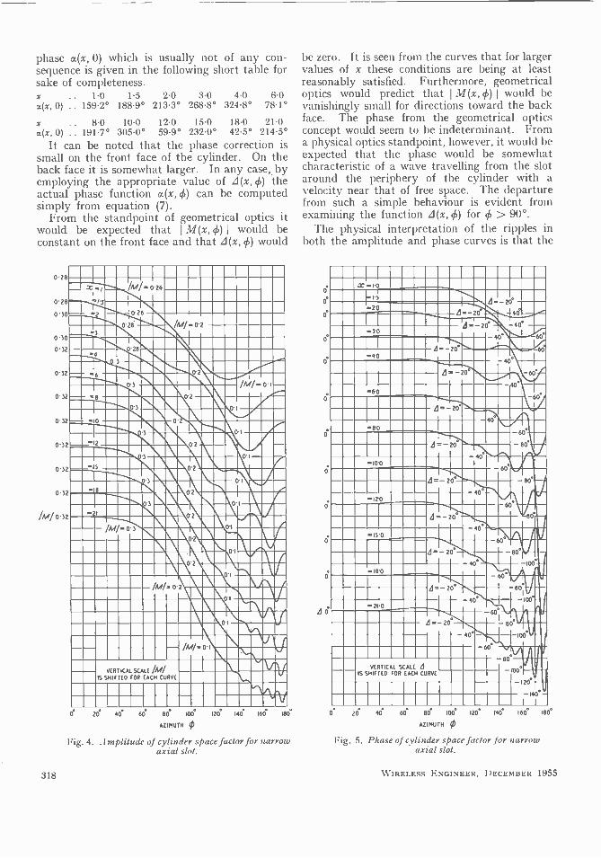
For larger values of x the convergence of the series formula for M becomes poor and something of the order of 2x terms are required to acquire three -figure accuracy. Another difficulty is that the I3essel functions are not adequately tabulated for large arguments and order. In this case it is necessary to employ recursion formulae to extend the tables slightly. Values of I M(x, 0): are shown plotted in Fig. 4 for x ranging from 1.0 to 21. The curves are displaced in the vertical direction to avoid any troublesome overlapping and to facilitate interpolation. To assist in reading the vertical scale, values of the ordinate IVI I are shown at appropriate places on the individual curves.
The nature of the curves is very interesting. As would be expected, the field in the geometrical shadow (0 > 90°) becomes successively smaller for increasing values of x. Furthermore, it can be seen that the ripples for the larger x values have a period of approximately 180/x degrees and the amplitude of the ripples is at a maximum at the back of the cylinder.
160
140
120
100
80
oc
60
40
20
e--- -L s..
\\
0 20° 40° 60° 80° 100°
AZIMUTH O Fig. 3. Phase of cylinder space factor for various values
of .r = ha sin O.
120° 140° 160° 180°
The phase function r.(x, ), as would be ex- pected, is a rapidly \ arving function of 0 for the larger x values. For this reason, it is desirable to express the phase as the sum of a simple, rapidly varying, function and a slowly varying part d (x, ¢) which is defined by a(x, 0) = a(x, 0) - 57.3 x(1 - cos 0) + d(x, 0)
degrees for 0 < 90° and a(x, 0) = a(x, 0) - x(57.3 + ' - 90°) 4- d(x, )
for 90° < < 180°. .. .. .. (7)
The function d(x, 0) is plotted in Fig. 5 for x ranging from 1.0 to 21. Again for convenience of presentation and for ease of interpolation, the curves are displaced vertically. The reference
317
phase a(x, 0) which is usually not of any con- sequence is given in the following short table for sake of completeness.
.. 1.0 1 5 2.0 3.0 4.0 6 0
a(x, 0) .. 159.2° 188.9° 213.3° 268.8° 324.8° 78.1°
x . . 8 0 10.0 12.0 15.0 18.0 21.0 (x, 0) .. 191.7° 305.0° 59.9° 232-1° 42.5° 214.5°
It can be noted that the phase correction is small on the front face of the cylinder. On the back face it is somewhat larger. In any case,, by employing the appropriate value of d(x, 0) the actual phase function a(x, 0) can be computed simply from equation (7).
From the standpoint of geometrical optics it would be expected that 114(x, 0) would be constant on the front face and that d(x, 0) would
0'28
0'28
0'30
0'30
032
032
032
0-32
03
0.3
0s
/M/ 0-32
318
L. 1Mt=0'z6
- X..,.
026 =Z
/M/=a2 a3
ozá
03
0 28
- 6
0-3 ._ -8
-1 al2 02 =15
.3 0z 01
=
03 0l
= 1 2 02
01
02
0' 1
/M/- 0 2
01
DI
0 }
VERTICAL SCALE /M/ IS SHIFTED FOR EACH CURVE
20 40" 60 80 100 120° 140° 160 180"
AZIMUTH 0
Fig. 4. Amplitude of cylinder space factor for narrow axial slot.
he zero. It is seen from the curves that for larger values of x these conditions are being at least reasonably satisfied. Furthermore, geometrical optics would predict that M(x, 0) I would be vanishingly small for directions toward the back face. The phase from the geometrical optics concept would seem to be indeterminant. From a physical optics standpoint, however, it would be expected that the phase would be somewhat characteristic of a wave travelling from the slot around the periphery of the cylinder with a velocity near that of free space. The departure from such a simple behaviour is eu ident from examining the function d(x, ck) for 0 > 90°.
The physical interpretation of the ripples in both the amplitude and phase curves is that the
ó
ó
0
ó
ó
ó
0
dá
S =IO
1'3 d- =ro
zó
d= zó ` ̀ ad 40°
=so 20
d
a0\ ...
-60°
_40 z- 60"
d - ' z- 40°
60°
-60 _ A_ 7im 60
8.0 ®L d- z-
=100 40O
- ', =120 60,
d_ -2o -q4 gig
=15 0 o -
d- 20° " 8á
=180 a0
uu aid d 20°
°60° 130
=21 0 40 ` ' 100
1
A
-60I 20 eó 4` 10Ó'
6' 1I VERTICAL SCALE d
80
IS SHIFTED FOR EACH CURVE IOO
120
I40*
1
0 20 40° 60 80 100° 120 140 160 180
AZIMUTH 0
F.g. 5. Phase of cylinder space factor for narrow axial slot.
\ IItELESS ENGINEER, 1)ECEM13E12 1955
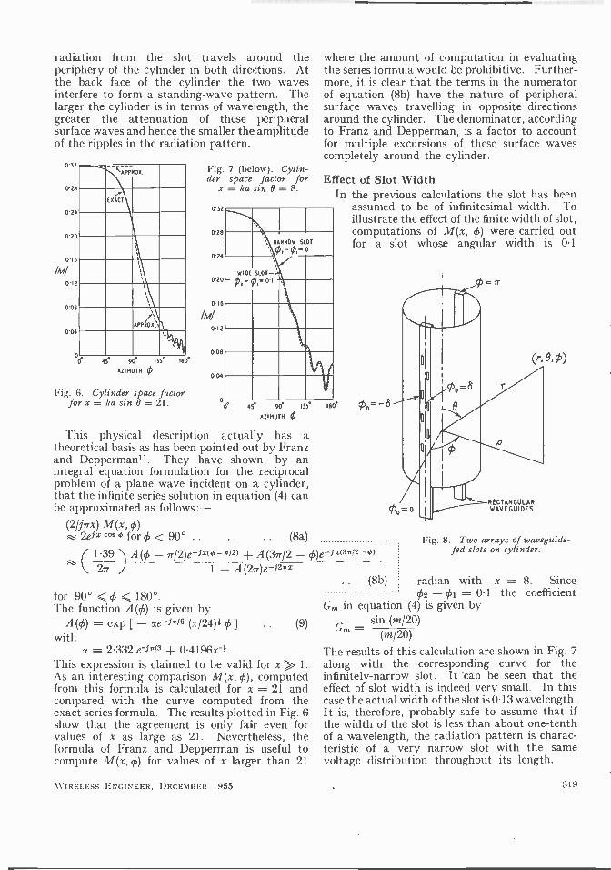
Fig. 7 (below). Cylin- der space factor for
x=ka sin O=8.
0'32
0 28
NARROW SLOT
024 -Oi=0 A
WIDE SLOT 020 - 0, -0i -0I .
0.16
/M/ 0 12
0 08
004
where the amount of computation in evaluating the series formula would be prohibitive. Further- more, it is clear that the terms in the numerator of equation (8b) ha\e the nature of peripheral surface waves travelling in opposite directions around the cylinder. The denominator, according to Franz and Depperman, is a factor to account for multiple excursions of these surface waves completely around the cylinder.
Effect of Slot Width In the previous calculations the slot has been
assumed to be of infinitesimal width. To fflustrate the effect of the finite width of slot, computations of M(x, 96) were carried out for a slot whose angular width is 0.1
45' 90' 135 180
AZIMUTH 0
This physical description actually has a theoretical basis as has been pointed out by Franz and I)eppermani1. They have shown, by an integral equation formulation for the reciprocal problem of a plane wave incident on a c} Linder, that the infinite series solution in equation (4) can he approximated as follows:-
(2/J7rx) M(x, (b)
a 2eix cos for <
radiation from the slot travels around the periphery of the cylinder in both directions. At the back face of the cylinder the two waves interfere to form a standing -wave pattern. The larger the cylinder is in terms of wavelength, the greater the attenuation of these peripheral surface waves and hence the smaller the amplitude of the ripples in the radiation pattern.
032
028
024
020
0'16
/M/ 0'12
0'08
0 04
'APPROX.
EXACT
APPROX.'
CO' 45 90 135' 180`
AZIMUTH 0
Fig. 6. Cylinder space factor for x = ka sin 8 = 21.
.. (8a)
-
1-39 A(4, - 7r/2)e-ix(n - "l2) + A (37r/2 - 0)e -J x(3'12-A)
.. (8b) radian with x = 8. Since (b1 = 0.1 the coefficient
G I in equation (4) is given by
G sin (nt/20)
(na/20)
The results of this calculation are shown in Fig. 7
along with the corresponding curve for the infinitely -narrow slot. It 'can be seen that the effect of slot width is indeed very small. In this case the actual width of the slot is 0.13 wavelength. It is, therefore, probably safe to assume that if the width of the slot is less than about one -tenth of a wavelength, the radiation pattern is charac- teristic of a very narrow slot with the same voltage distribution throughout its length.
27r 1 -A (27r)e-12'x
for 90° < G 180°. The function A (0) is given by
A(ck) = exp [ - 7.e -J"6 0"/24)l 7
with
o0-
-n
RECTANGULAR WAVEGUIDES
(9)
= 2.332 e"13 + 04196x-3 .
This expression is claimed to be valid for x 1. As an interesting comparison M(x, 95), computed from this formula is calculated for x = 21 and compared with the curve computed from the exact series formula. The results plotted in Fig. 6 show that the agreement is only fair even for values of x as large as 21. Nevertheless, the formula of Franz and Depperman is useful to compute M(x, 0) for values of x larger than 21
\\'ERH:I.E3sS ENGINEER, 1)ECEMEiEI! 1955
Fig. 8. Two arrays of waveguide- fed slots on cylinder.
319
Arrays of Slots The numerical results shown graphically in
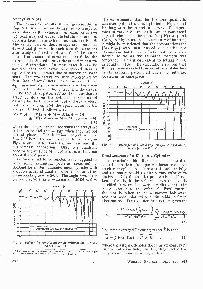
Figs. 2 to 6 can be readily applied to arrays of axial slots on the cylinder. An example is tso identical arrays of waveguide-fed slots located on opposite faces of the cylinder as shown in Fig. 8. The centre lines of these arrays are located at (A.o = 0 and 00 = 7r. In each case the slots are alternately displaced on either side of the centre lines. The amount of offset is dictated by the nature of the desired form of the radiation pattern in the O direction9. In most cases it can be assumed that each array of displaced slots is equivalent to a parallel line of narrow collinear slots. The two arrays are then represented by four lines of axial slots located in azimuth at to = +S and ¢o = 7r ± 8 where S is the mean offset of the slots from the centre line of the arrays.
The azimuthal pattern Ma(x, 0) of this double array of slots on the cylinder is determined entirely by the function M(x, 0) and is, therefore, not dependent on S(B) the space factor of the arrays. In fact, it follows that Ma(x, 0) = [M(x, + 8) + M(x, - 8)] f [M(x, + 77 + 8) + M(x, + 7r - 8)]
.. .. .. (10) where the + sign is to be used when the arrays are fed in phase and the - sign when they are fed out of phase. The function i Ma(21, 0) I for S = 2.0° is plotted on a relative decibel scale in Figs. 9 and 10 for both the in -phase and the out -of -phase connection. Only one quadrant need be shown since Ma(x, 0) is an even function about the 90° points.
W. Searle and R. G. Sinclair have supplied us with some azimuthal patterns measured at X -Band for an 8 -in. diameter metal cylinder with a double array of axial slots with a mean offset corresponding to S ti 2.0°. The angle B was kept constant at 805° so x = ka sin 0 = 20.96 N 21*.
O.
AZIMUTH 0 10' 20 30' 40 50° 60' 70 80 90
z
6
e
10
Iz
14
-THEORETICAL EXPERIMENTAL (AVERAGE OF 4 QUADRANTS)
16
A 18
,,,
-
Fig. 9. Pattern for two slot arrays on cylinder fed in phase (ha sin 9 = 21).
'The arrays were designed to produce a main lobe at the angle o - 80.5° neglecting diffraction :wound the cylinder.
320
Che experimental data for the four quadrants was averaged and is shown plotted in Figs. 9 and 10 along with the theoretical curves. The agree- ment is very good and so it can be considered a good check on the data for I M(x, 56) I and oE(x, 0) in Figs. 4 and 5. As a matter of interest, it might be mentioned that the computations for Ma(x, 0) 1 were first carried out under the
assumption that the slot offsets need not be con- sidered so far as the azimuthal pattern was concerned. This is equivalent to setting 8 = 0 in equation (10). The calculations showed that this approximation led to errors of several decibels in the azimuth pattern although the nulls are located in the same place.
AZIMUTH
10 20 30 40 S0 60
o
2
4
m 6
8
10
LL 12
- 14
16
18
20
22
24
70 80 90
- THEORETICAL EXPERIMENTAL (AVERAGE OF 4 QUADRANTS)
Fig. 10. Patters for two slot arrays on cylinder fed out of phase (ka sin B = 21).
Conductance of a Slot on a Cylinder To conclude this discussion some mention
should be made of the input conductance of slots on circular cylinders. To treat this problem fully and rigorously would require a very exhaustive analysis. Only the exterior problem is considered here; that is, if the voltage across the slot is specified, how much power is radiated into the space exterior to the cylinder? Furthermore, the slot is taken to be a narrow half -wave resonant axial slot with a sinusoidal voltage distribution. The radiation field is then given by
e -i kr Vo COS (
Z cos o)
E 7r2 rk sin2 B a
m=
e na, in cos nub Hna(2>'(ka sin 0)
.. (11)
The time -averaged Poynting vector S is then 1
S = Real Part of E x H* . . . (12)
where the asterisk denotes the complex conjugate. In the radiation field, the Poynting vector has only a radial component Sr so that
-V -
\\'TRELEss ENGINEER, DECEMBER 1955
Sr = 1 E* .. .. (13)
770
for r tending to infinity. The radiated power P is then obtained, in the usual way, by integrating over a spherical surface. This leads to
Vol cost (cos 0
J'0 f2 0 ' Y27r4k2 s1I14 942
/
The curves of the `cy:inder space factor' are presented in a form in which they should have wide applicability.
Acknowledgments I would like to thank Messrs. R. M. Dohoo,
\V. Searle and R. G. Sinclair for making available their experimental results and for their helpful comments. Mr. \V. A. Pope and Miss M. O'Grady
assisted with the numerical work e a
E 7Ze5i201- no cos n cos ntq r2 sin 0 dOdO
=o ó [HU21 [Hna2']*
which, following an integration with respect to 0, takes the form
P= V02 cose C 2
cos 0)
27j07r3 k2a2 0 sin3 0 n=011-1 n2/(ka sin 0) ; 2
The external radiation conductance G is then defined by
G = 2P/V02. Lmploying numerical integrations of equation (15), values of G were computed for various ka values between 0.1 and 21. The limiting value for very small linders is seen from equation (15) to be given by
60 COS 1 2 cos 0) G= \ d0, (16)
'io- J o sin O
which is the same integral that arises in a thin half -wave wire aeria112. The radiation conduct- ance for infinitesimally small cylinders is then given by
G]xa o = 73.13/77o2 = 0.514 milli -mho, where it will be immediately recognized that the 73.13 can be identified with the radiation resistance in ohms of the complementary wire aerial. This simple equation is a statement of Babinet's principle. At very large values of ha the cylinder, so far as the slot is concerned, is equivalent to an infinite plane conducting surface. Following the reasoning of Bookerl3 it would be expected that
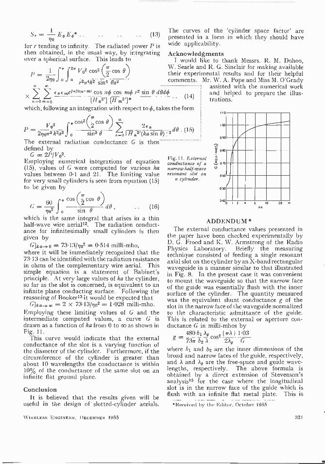
G]ka , co = 2 X 73.13/7j02 = 1.028 milli -mho. Employing these limiting values of G and the intermediate computed values, a curve G is drawn as a function of ka from 0 to 0o as shown in Fig. 11.
This curve would indicate that the external conductance of the slot is a varying function of the diameter of the cylinder. Furthermore, if the circumference of the cylinder is greater than about 10 wavelengths the conductance is within 10% of the conductance of the same slot on an infinite flat ground plane.
Conclusion It is believed that the results given will be
useful in the design of slotted -cylinder aerials.
WIRELESS ENGINEER, DECEMBER 1955
(14)
d0 . (15)
Fig. 11. External conductance of a narrow half -wave resonant slot on
a cylonder.
and helped to prepare the illus- trations.
110
I' OO
o vo
É 0 8 w£ 0 70
0'50
oso
0400 1 2 4
J
6 l0 ka
20
ADDENDUM *
The external conductance values presented in the paper have been checked experimentally by D. G. Frood and R. \V. Armstrong of the Radio Physics Laboratory. Briefly the measuring technique consisted of feeding a single resonant axial slot on the cylinder by an X -band rectangular waveguide in a manner similar to that illustrated in Fig. 8. In the present case it was convenient to mount the waveguide so that the narrow face of the guide was essentially flush with the inner surface of the cylinder. The quantity measured was the equivalent shunt conductance g of the slot in the narrow face of t he waveguide normalized to the characteristic admittance of the guide. This is related to the external or aperture con- ductance G in milli -mhos by
180biay 2(Ira) 1.03 g 737r b2
cos 2A G
where h1 and b2 are the inner dimensions of the broad and narrow faces of the guide, respectively, and 7A and Ag are the free -space and guide wave- lengths, respectively. The above formula is obtained by a direct extension of Stevenson's analysis15 for the case where the longitudinal slot is in the narrow face of the guide which is flush with an infinite flat metal plate. This is
*Received by the Editor, October 1955
321
equivalent to an infinitely large cylinder (ka -> co) where 1.03/G in the above formula would tend to unity.
In the experiment, A = 3.2 cm, A,, = -1'68 cm, bl = 0.9 inches, b2 = 0.4 inches, and therefore g = 1.28/G. The dimensions of the slot were 2/3 in. x 1/16 in. Denoting dg as the difference between g for arbitrary ka and g for ka = oo, the comparison between theory and experiment is shown in the following table:
ha
dg Values
2.5 3 5 7 9 14
Experiment 0.13 0.09 0.06 0.05 0.05 0.02
Theory 0.15 0.12 0.08 0.05 0.04 0.02
The agreement here is quite reasonable. The departure at the smaller ka values can probably be accounted for by the non -resonant condition of the slot in which case g and G 'would not be inversely proportional.
The effect of the finite length of the cylinder
was also investigated experimentally. It was found that the measured conductance was essentially independent of length L if L > 3a.
REFERENCES A. Alford, "Long Slot Antennas", 1'r«. Nat. Electronics Conf.,
Chicago, Ill., 1946, Vol. 2, pp. 143-155. A. A. I'istolkors, "Radiation From a Transverse Slit on the Surface
of a Circular Cylinder", J. Tech. Whys., U.S.S.R., 1947, Vol. 17, pp. 377-388 (in Russian).
' George Sinclair, "The Pattern of Slotted -Cylinder Antennas", Prow. Inst. Radio Engrs, 1948, Vol. 36, pp. 1487-1492.
' C. H. Papas and Itonold King, "Currents on the Surface of an Infinite Cylinder Excited by an Axial Slot", Quart. Appi. Math., 1949, Vol. 16, pp. 175-182.
° C. H.. Papas, "Radiation from a Transverse Slot on an Infinite Cylinder", J. Math. Phrs., 1950, Vol. 28, pp. 22/-236.
J. R. Wait, "Radiation From a Slot on a Cylindrically Tipped Wedge", Canad. J. Phrs., 1954, Vol. 32, pp. 714-721.
' S. Silver and W. K. Saunders, "Field Produced by a Transverse Slot ofta Circular Cylinder", J. Appi. Phys., 1950, Vol. 21, pp. 745-749.
L. L. Bailin, "Field Produced by a Slot on a Large Circular Cylinder", Trans. I.R.E. (PGAP), Vol. AI' -3, July 1955, p. 128.
W. H. Watson, "Physical Principles of Wave Guide Transmission and Antenna Systems", Oxford University- Press, 1947.
° "Scattering and Radiation From Circular Cylinders :,,td Spheres", Math. Tables Proj. and M.I.T. Underwater Sound Laboratory, 1945.
" W. Franz and K. Deppertnan, "Theorie der Beugung am Zylinder outer 13eriicksichtiguttg der Kriechwcllc", Ann. der I'hysik, 1952, Vol. 10, pp. 361-373.
J. A. Stratton, "Electromagnetic Theory", McGraw-Hill Book Co., Net,' York, 1941.
" H. G. Booker, "Slot Aerials and Their Relation to Complementary \\'ire Aerials", J. lush elect. Engrs, 1946, Vol. 93, Pt. ILIA, No. 4, pp. 620-626.
" S. A. Schelkunoff, "Electromagnetic Waves", Van Nostrand Co. Ltd., N.\ ., 1943.
" A. F. Stevenson, " Theory of Slots in Rectangular Waveguides", J. App!. Phys., 1948, Vol. 19, pp. 24-38.
APPEN Although the derivation of the expression for the
radiation field of an axial slot is implicit in the previously - mentioned papers, it seems worth while for the sake of completeness to outline a proof. Furthermore, the method used here does not rely on the use of the reci- procity theorem and therefore' is of general interest.
The starting point is to consider a magnetic dipole of moment Kdzn where dzu is the equivalent length of the element of magnetic current Li as defined by Schelkunofftt. With respect to the (p, ¢, z) co-ordinate system, the dipole is located at (flu, ¢o, z0) and is oriented in the z direction. The surface of the conducting cylinder of infinite length is defined by p = a where a
The primary magnetic vector potential of the dipole has only a z component F and is given by
1'r, = Kdzue-it-, 4nrt
where
rt=1Pt'+(Z--)211 and
(IA)
Pi= 1P2 + Po' - 2PPo cos (41. - 960)11 .
The resultant potential has only a z component F and is a solution of the inhomogeneous Helmholtz wave equation
Kdzo 8(r-ro) (72 + kz) 1' = - - 4n
(2A)
where r and ru are vectors extending front the origin to the point of observation and the source points respectively. 8(r - ro) is the three-dimensional impulse function. The resultant fields arc gi\ en by
1 OF OF lip = - P
. - Fm , = óp--
, 1=: = 0, 60,
a2F a2F h2 JµwHp = ópbz-
, JµwHm = pb5bbz' JP°wH:= (k2 + az2) F.
.. (3\ )
322
DIX The function F must now he constructed so as to be a
solution of the inhomogeneous wave equation and to satisfy the boundary condition that the tangential electric field (i.e., lam) vanishes on the conducting surface, that is
bp - =oat p = a. P
The function F is now expressed as a combined Fourier integral and series as follows
I' (P, 56, z) =,tl '+ roe
_n - 1h(z- i,) e,,,I',,,(P) 27,
cos In (4, -0n)
.. (4A) where F,,, is a Fourier coefficient which is a solution of the equation
l
op P ap+ (k2 h')P -' ']1:,,.(P) = - a(P - Pu)
.. . (5A) Solutions of equation (5.\) which possess a vanishing normal derivative p = a are
11
F,,,(P) =C,,,H,,,t2t(up) L.I
s,(trpo) -H,nl1(uPo) f,,,'(lra)J for p>Pu H,,,t2 '(ua)
z (up) = C,nH,,,t21(tsPo) f,,,(trP) - H,,,tz1' (isa).,,,'(ua)
for P < Po
.. (6A) where = (k2 - 1t2)1t2, J,,, is the Bessel 1' unction of the first type of order in and H,"Izl is the Hankel function of the second kind of order ni. The factor C,,, can be found by integrating, with respect to p, both sides of equation (5A) over a small interval which includes pu. This process yields
C,,, _ -742. The resultant magnetic vector potential is then
completely given by
,,,=o
\VIKELESs 1?NG1NEEK, 1)Et.EMHEIe 1955
_ F-- ,,, cos ,(d,- 4,o)< I
iI,'-'(arP)[.l,(¡rpo) - 11,,,(2i(upo) H ,' -r ,/,' (Ha)
2 "
- zrn)J
for p > Po. 'Ile solution for the case p < po is obtained by interchanging p and po where they occur in equation (7A). This constitutes the exact solution for the problem of a magnetic dipole parallel to a circular conducting cylinder. Since this result has not apparently been given elsewhere, it is of some interest in its own right.
The above formal solution is simplified somewhat if the fields are observed at a large distance from the cylinder. The square bracket term in the integral is then a slowly varying function of b compared to the other factors. The saddle point of the integrand is then at h = k cos O where O = tan-' p/(z - z ). The integration can then he Carried out to yield
Kdzo e -jkR - L> 47r 1?
U
;Mt (7A)
Kdzelk cos Oz. e ikI' `, e,,, cos u,(4, - Mein'nl2 t^t, - an' H L, ,,, (ha. sin )
ut _11
.. (9A) where use has been made of the \Gronksian relation
H,'92) .1,,, (x) - H,'=t' (a) ./, (x) = 21/7,2. By employing Schelkunoff's equivalence theorem it can be seen that the axial magnetic current K at z is equivalent to a thin axial slot on the cylinder of length dzo excited by a transverse voltage I'(zo). The extension to an axial slot of finite length from z, to z, is effected by integrating over z. Furthermore, if the slot is of
e,"P1m7,12 Cos nr(ck - )eikz 105 e j,(kPo sin 8) - H,'-'
(k p sin O).1,,,'(ha sin B) .. (5A) [ H,i2(basin B)]
where I? = (p' -I z9'1- and which is valid for Pp sin O
I. To the same order of approximation, the fields are
given by E -jk sin B F and iIo - k F. ,. 1'le
other field components are of order I /N- so they can be neglected in the far field.
\\ hen the magnetic current element is located on the surface of the cylinder (p = a), the radiation field can be written
finite width the integration must st also he carried out over ¢ from 0, to ¢-. It is assumed here, for convenience, that the transverse field in the slot is uniform. It then follows that
R = l'(z)elk cos 0. dz
277.2a /? Z,
sin [u,(02 - ¢,1/2: e.ei'° Iº cos ur(,b - 0) X
fni(0- - ,);2] H,'-"(ka sin 8) - (lo.\)
where ¢o = (02 + 012
EQUIVALENT EQUALIZER NETWORKS By R. O. Rowlands, M.Sc., A.M.I.E.E.
(N.B.C. Enginrrring Training Dept.)
1. Introduction WHERE a signal suffers attenuation and
phase distortion, equalizers are inserted in the circuit to correct for either or
both forms of distortion. Instead of obtaining the full amount of correction with one complex network it is often more convenient to synthesize the required characteristic from those of simpler networks. This may be clone in two distinct ways.
(a) The normal procedure is to use constant - resistance networks connected in tandem. This method has the advantage that if the attenuation- frequency response of the simple networks have been calculated in dB and graphs drawn, the end -to -end response is the sum of the individual curves.
(h) An alternative method is to connect a number of very simple circuits (such as dif- ferentiating circuits) in tandem, pass the signal through such an arrangement and combine the signals which appear at the various junctions- including the input-in varying proportions as
MS accepted by the Editor, February 1955
WIRELESS ENC:INI?I?rt, I)LCE>IHErt 1955
shown in the block schematic diagram of Fig. 1. The overall response will then be the algebraic stun of the individual responses calculated on a linear basis. This method was suggested by Gouriet' and for certain applications it has special advantages, in particular, extreme flexibility. The various types of frequency -response curves obtainable with practical networks of this kind will now be analysed and the equivalent constant - resistance networks derived for comparison since the performance of these latter networks is well known. In the analysis which follows, the symbol p will be used throughout for jw.
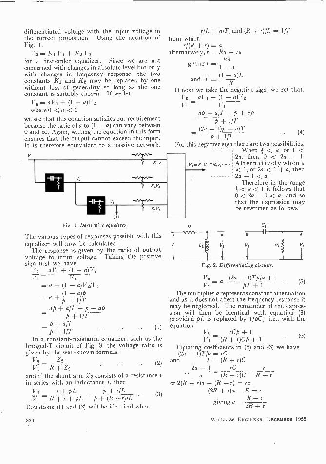
2. Equalizer of the 1st Order Either of the two differentiating circuits of
Fig. 2 may be used. Both give the same result, viz.:
z -
PI -2 where I /1' _ /t f
1' 1 7] + pL'-' p + l/l L2
and 1
R2
p+117. where 7'=I:2C1
Equalization is achieved by combining the
323
differentiated voltage with the input voltage in the correct proportion. Using the notation of Fig. 1.
bo=K1 1á'1+A2>'2 for a first -order equalizer. Since we are not concerned with changes in absolute level but only with changes in frequency response, the two constants K1 and K2 may be replaced by one without loss of generalit\ so long as the one constant is suitably chosen. If we let
Vo = aVi + (1 - a)V2 where 0 < a <1
we see that this equation satisfies our requirement because the ratio of a to (1 - a) can vary between 0 and co. Again, writing the equation in this form ensures that the output cannot exceed the input. It is therefore equivalent to a passive network.
V,
Fig. 1. Derivative equalizer.
The various types of responses possible equalizer will now be calculated.
The response is gi\ en by the ratio of output voltage to input voltage. Taking the positive sign first we have
Vo_aVi+(1-a)1.2 1'1 Vi
= a + (1 - a)V2/ICI -a+(1 -a)p
p + 1/7.
ap+elT +p- _--- p
p+al7' 1/7
In a constant -resistance equalizer, such as the bridged -T circuit of Fig. 3, the voltage ratio is given by the well-known formula
Vo Z2
Vi R + Z2
and if the shunt arm Z2 consists of a resistance r in series with an inductance L then
Vo r+pL p+r/L 1/1=R+r+pL p+(R+r)/L
Equations (1) and (3) will he identical when
324
with this
(I)
(2)
(3)
rIL = a/T, and (R rt r)II- = 1/T
from which ri(R + r) = a
alternatively, r = Re ± re Re
giving r =- 1 - a (1 -(/)L
and T =
I f next we take the negative sign, we get that, Ifo a 1 - (1 - (1)1'2 y;i = l_i--
For this
ap+a/T-p+ap - p -+-1 /T
(2a - 1)p + a/T p
(4)
negative sign there are two possibilities. \Vhen < a, or 1 <
2a, then 0 < 2a - 1.
Alternatively when a < 1, or 2a < 1 + a, then
V0 =K1 V,±KzVZ
2a - 1 < a. Therefore in the range < a < 1 it follows that
0 < 2a - 1 < a, and so that the expression may be rewritten as follows
C,
Fig. 2. Differentiating circuits.
Vo (2a - 1)Tp/a + 1 V1=a.. ..
'I he multiplier a represents constant attenuation and as it does not affect the frequency response it may be neglected. The remainder of the expres- sion will then be identical with equation (3) provided pL is replaced by 1 pC; i.e., with the equation
Vo_ rCp+l V1 (R + r)Cp + 1
Equating coefficients in (5) and (6) we have (2a - 1)T la = rC
and T = (1? + r)C 2a - 1 rC r
!I r)C or2(R+r)a-(R+r)=ra
(2R+r)a=R+r R+r
giving =.l,
.. (6)
\VIRELESS ENGINEER, DECEMBER 1955
In this case the attenuation-frequency curve slopes in the opposite direction to that obtained by adding the voltages.
However, when 0 < a < 1, then 2a - 1 is negative and equation (3) may be rewritten,
Vo a/7'- (1 - 2a)p a - (1 -2a)pT V1 1/T+p 1+pT
multiplying numerator and denominator by a + (1 - 2a)pT, we get
Voa+(1-2a)pT a-(I-2a)p'1' V1 1 + pT a + (1 - 2a)pT
The first expression corresponds to the charac- teristics of one of the two constant -resistance equalizers already discussed depending upon the relative values of a and (1 - 2a).
If a > 1 - 2a (i.e., a > 1/3) the attenuation increases with frequency.
If a < 1/3, the attenuation decreases with frequency, while if a = 1/3, the attenuation is constant. In the second expression the modulus of the numerator is equal to that of the denomin- ator and so it represents a network which gives a phase change with no attenuation. This can be produced by a constant -resistance lattice section having series and lattice arms consisting of an inductor and a capacitor respectively, where L = R7', and C = T/R, R being the image impedance of the lattice.
3. Equalizer of the 2nd Order If the differentiated voltage V2 is passed through
a second differentiating circuit, the output voltage V3 will be given by,
V3 p p where S= 1 T V2 p + 117'2 p +S2 (/ ) V3_ V2 V3_ p p V1 - V1 V2 - p + Si p + S2
p2
(p + Si) (p + S2) And if Vo = K2V2 f K3V3
(the K terms being positive fractions)
Then V0=Ii1 + K2 + K3 V2 V3
V1 V1 Vl
= 11 f I'2p + K3 p2
p + S1 (p + Si) (p + S2)
Ki(p + Si) (p + S2) f K2p(p - S2) f K3p2
(p + s1) (p + S2) which may be written
Vo a(p2+1'p+c) V 1 (p + Si) (p + S2)
Where a=K1+li2+li3 h = (K1S1+K1S2fK2s2)/(K1fK2iK3)
and c = K1S1S2/(K1 +1K2 ±[K3)
wIRELESS ENGINEER, DECEMBER 1955
. (7)
It will be seen that all values are possible for 1, and c and so the quadratic in the numerator of equation ;7) is perfectly general. If it is capable of being factorized it may be rewritten as follows, the factor a being ignored.
Vo (P + 71) (P + x2)
V1 (p + Si) (p + S2)
p+x1 . p+a2 p+S1 p+S2
The equivalence of each part of this expression to the response of a constant -resistance equalizer network with or without a phase -shift network has already been established. The response corresponding to the whole expression will therefore be produced by these networks connected in tandem. It does not matter which value of a is associated with which S, the overall response will he the same although the individual networks used will vary with the combination chosen.
Fig. 3. Bridged -T equalizer. Fig. 4. Shunt arm Z2.
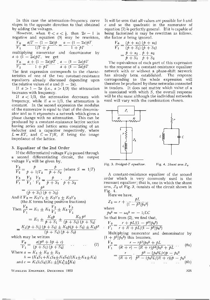
A constant -resistance equalizer of the second order which is ver\ commonly used is the resonant equalizer; that is, one in which the shunt arm, /.2 of Fig. 3, consists of the circuit shown in Fig. 4.
Here we have,
I2-I +(1-p2/po2)
where Po' = - woe = - 1/LC
So that from (2), we find that, Vo I" + pL/(1 - p2/15o2)
I'1 - r + R + pL/(l - p2/po2) Multiplying numerator and denominator by
(1 + p2/po2) this becomes, Vo r -1p2/ o2+pL V 1 (R + r) - (R + r)p2/pot + pL
. .
_/j2 - (po2L/r)p - po2
(R + r) p2 - (p02L 'i? + r))p - po2 .. (Sb)
pL
(8a)
325
Comparing this with equation (7) we find that for the equations to be identical, the constant terms in the numerator and denominator of (7) must be equal,
K1S1S2 i.e. lí1+ K2 +K3
or Iii=Kl+K2+K3 giving K2 = - K3
Again, the coefficient of p in the numerator of equation (8b) is greater than that in the denominator.
Applying this condition to equation (7) we get that,
Ii 1S1 + K1S2 + K2S2 > S1 + Sz K1+K2+K3 and making use of equation (9),
KS1 + K1S2 + K2S2 > KIST + K1S2 Therefore the positive sign must be attached to
K2.
Again, the coefficient of p in the numerator of equation (8a), is equal to that in the denominator.
Applying this condition to equation (7), we get that a.h=Si+S2 i.e., K1S1 + K152 ± K2S2 = Sl + S2 i.e., ± K2S2 = (S1 + S2) (1 - K1)
and since K1 < 1, the negative sign on the left- hand side may he omitted.
K2=(s1s x2)(1-KI) .. (10)
The equivalent of the resonant equalizer is thus given by,
= SIS (9)
S1 + Sz Vo=h1V1+
S2 (1-Ií1)(V2-1'3)
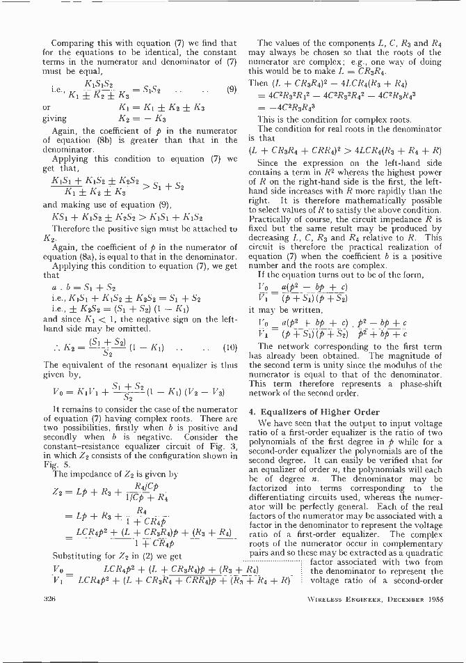
It remains to consider the case of the numerator of equation (7) having complex roots. There are two possibilities, firstly when h is positive and secondly when h is negative. Consider the constant-resistance equalizer circuit of Fig. 3, in which Z2 consists of the configuration shown in Fig. 5.
The impedance of Z2 is given by R4/Cp
Z2 = Lp + R3 + W7)-± -
R4 =Lp+I¿3+1+CI14P-
LCR4p2 + (L + CR3R4)p + (R3 + R4) = CR4p
- - Substituting for Z2 in (2) we get
The values of the components L, C, R3 and R4 may always be chosen so that the roots of the numerator are complex; e.g., one way of doing this would be to make L = CR3R4. Then (L + CR3R4)2 - 4LCR4(R3 + R4) = 4C2R32R42 - 4C2R32R42 - 4C2R3R43 = -4C2R3R43 This is the condition for complex roots. The condition for real roots in the denominator
is that (L + CR3R4 + CRR4)2 > 4LCR4(R3 + R4 rt R)
Since the expression on the left-hand side contains a term in R2 whereas the highest power of I? on the right-hand side is the first, the left- hand side increases with I? more rapidly than the right. It is therefore mathematically possible to select values of I? to satisfy the above condition. Practically of course, the circuit impedance R is fixed but the same result may be produced by decreasing L, C, R3 and R4 relative to R. This circuit is therefore the practical realization of equation (7) when the coefficient h is a positive number and the roots are complex.
If the equation turns out to be of the form,
a(p2 - hp + c) VI (p +si) (p + s2)
it may be written,
Vo a(p2 + hp + c) . p2 - by + c VI (p+sI)(p+s2) p2+tip+c The network corresponding to the first term
has already been obtained. The magnitude of the second term is unity since the modulus of the numerator is equal to that of the denominator. This term therefore represents a phase -shift network of the second order.
4. Equalizers of Higher Order \\'e have seen that the output to input voltage
ratio of a first -order equalizer is the ratio of two polynomials of the first degree in p while for a second -order equalizer the polynomials are of the second degree. It can easily be verified that for an equalizer of order n, the polynomials will each be of degree u. T11e denominator may be factorized into terms corresponding to the differentiating circuits used, whereas the numer- ator will be perfectly general. Each of the real factors of the numerator may be associated with a factor in the denominator to represent the voltage ratio of a first -order equalizer. The complex roots of the numerator occur in complementary pairs and so these may be extracted as a quadratic
factor associated with two from Vo L CR4 p2 + (L + CR3R4)p + (R3+ R4) v, LCR4 p2 + (L + CR3R4 + CRR4) p + (R3 + R4 + R)
326
the denominator to represent the voltage ratio of a second -order
\\TIRELESS ENGINEER, DECEMBER 1955
equalizer. Equalizers of a higher order than the second do not therefore contribute a new type of characteristic but are equivalent to a ]cumber of first- and second -order equalizers connected in tandem.
Ri
V Cz ` Vz T Fig. 5. Pig. 6.
Shunt arm 7z. Integrating circuit.
5. Integrating Circuits All the characteristics obtained with differenti-
ating circuits may also be obtained with integrating circuits, for example, the integrating circuit of Fig. 6 gives the equation,
V2 1/pC2 1
V1 RI + 1/pC2 - R1C2p +1
1 where T = R1C2 p + 1/T
and n such circuits will give
Vn+1 1
V1 (p + 1/T)n
Combining this with the input we get,
K1V1 ± Kn+1Vn+1 Ki(p+ 1/T)n i Ian +1 = (p + 1IT)"
This is the ratio of two polynomials of degree n and the inclusion of the intermediate terms in the numerator can make this perfectly general.
6. Summary The equivalence of the two methods of equaliza-
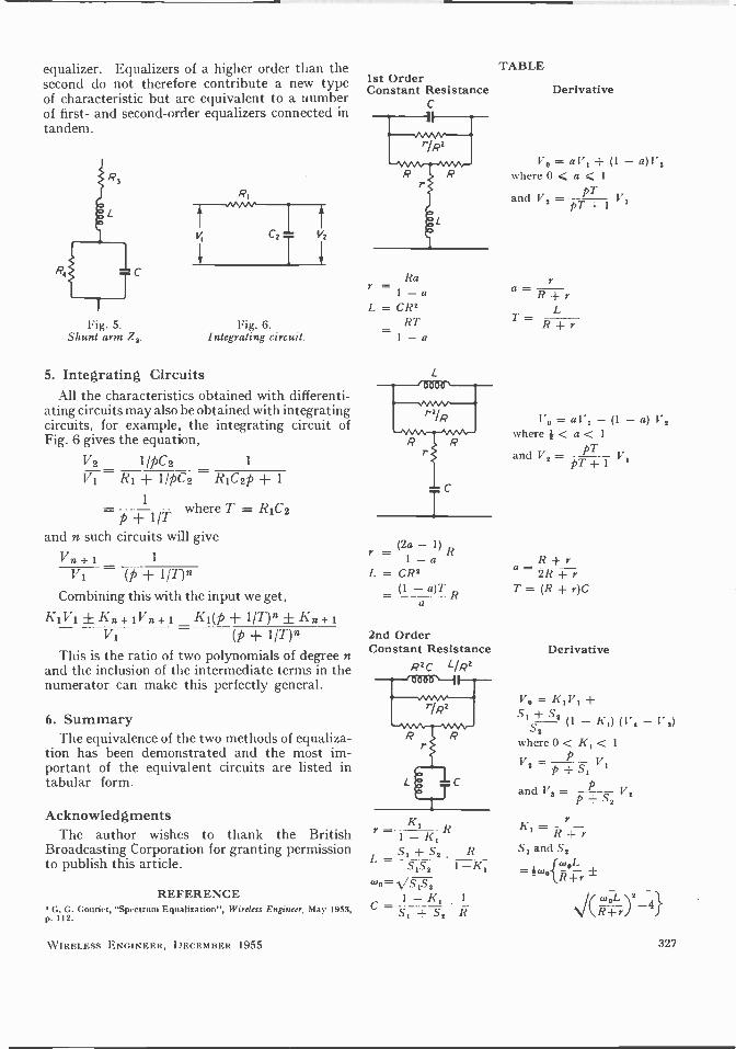
tion has been demonstrated and the most im- portant of the equivalent circuits are listed in tabular form.
Acknowledgments The author wishes to thank the British
Broadcasting Corporation for granting permission to publish this article.
REFERENCE G. G. Couriet, "Spectrum Equalization", Wireless Engineer, May 1953,
p. 112.
WIRELESS ENGINEER, DECEMBER 1955
1st Order Constant Resistance
C
Ra r =
L = CR' RT
- I - a
r =(2a- IR 1 - a
I_=CRz (1 -a)TR
a
2nd Order Constant Resistance
R2 LIP'
K1 r= R
=S1 -f Sz R S1Sz 1 -K,
wtl- VJ IS I -K1 l
.r, --1S, , -L S, R
TABLE
Derivative
Vo = a VI (I - a) V,
where 0<a< 1
and V_, = -p V1 1
IVo = aV, - (1 - a) Vz
where < a < 1
and Vz - pT V,
R -}- r a = ?tt-+r T=(R-Fr)C
Derivative
V, = I ,1't 4-
S + SZ (1 - K,) (1'z - 1'2) SZ
where 0 < K, < 1
p Vz = S,
V,
and Vz = p_71) S,
VI
=iz+r S1 and S2
- wul. -awo R+r ±
J\R+T/9-4f
327
SATURABLE -REACTOR FREQUENCY DIVIDER
By G. W. G. Court*, B.Sc., A.M.I.E.E.,A.Inst.P. and C. I. C. Scollay j-, B.E.,B.Sc., A.M.I.E.E. (Department of Scientific and Industrial Research, New Zealand)
SUMMARY.-A saturable reactor in conjunction with a simple resistance -capacitance network will provide a frequency -dividing circuit capable of producing a pulse output at the frequency, or submultiple of the frequency, of an input sinusoidal voltage waveform.
The circuit \vas initially devised as a means of synchronizing the pulse repetition frequency of a radar modulator at half the power supply frequency but has other applications where frequency division of this kind is required.
General THE saturable reactor is well known as a
result of the original paper by Melville' ;
its essential characteristics may be briefly summarized by reference to Fig. 1 which shows the idealized form of the B-H characteristic of a
magnetic material B 5 T. such as H.C.R.
metal. The initial part of
the curve OS is H linear and, following
the sharp 'knee' at S, the characteristic
T'
Fig. 1. Idealized B -H curve of H.C.R. material.
SI remains parallel to the H axis. An inductor having a magnetic circuit of material of this type will have the following features.
The incremental inductance when the core material is operated in the regions OS and OS' will be constant and can be referred to as L,,. In the region ST and S'T' the core material is saturated and the incremental inductance becomes Ls which approaches zero.
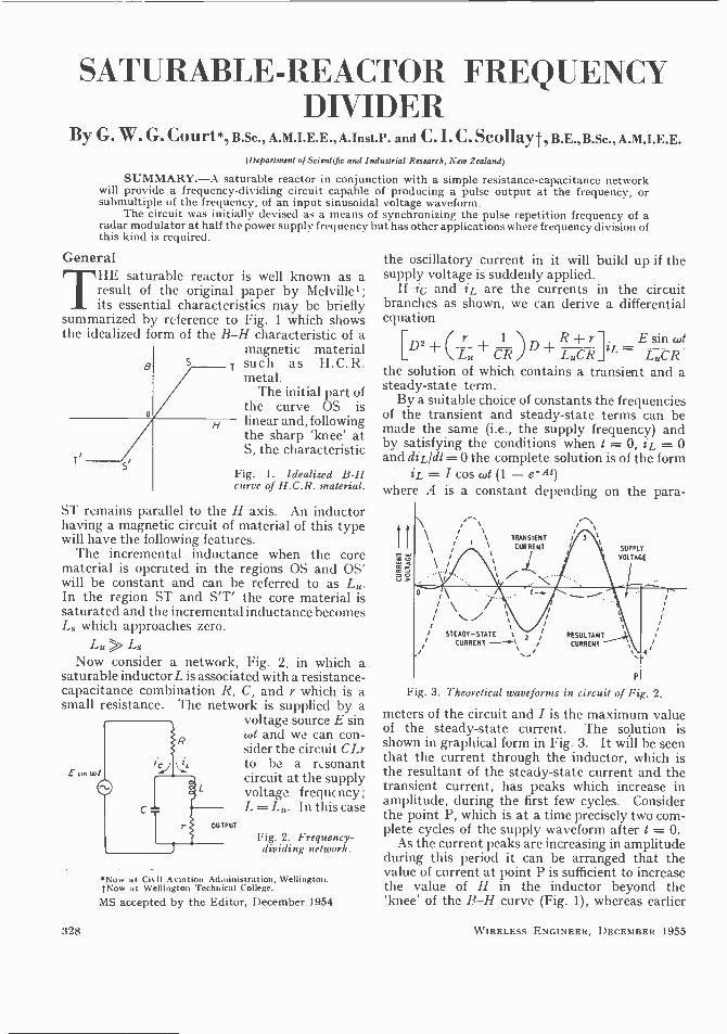
L,1 Ls Now consider a network, Fig. 2, in which a
saturable inductorL is associated with a resistance - capacitance combination R, C, and r which is a small resistance. The network is supplied by a
voltage source E sin wt and we can con- sider the circuit CLr to be a resonant circuit at the supply voltage frequency; L = Ln. In this case
Fig. 2. Frequency - dividing network.
*Now ;,t Civil Aviation Administration, Wellington. 1 -Now at Wellington Technical College.
MS accepted by the Editor, December 1954
328
the oscillatory current in it will build up if the supply voltage is suddenly applied.
If is and iL are the currents in the circuit branches as shown, we can derive a differential equation
r 1 R+r1 _E sin cot [D2 + LI,+CR)D+LnCRJ1L LCR
the solution of which contains a transient and a steady-state term.
By a suitable choice of constants the frequencies of the transient and steady-state terms can be made the same (i.e., the supply frequency) and by satisfying the conditions when t = 0, iL = 0 and diLicit= 0 the complete solution is of the form
iL = I cos wt (1 - e- At)
where A is a constant depending on the para-
o
/ \\ TRANSIENT / t
\ CURRENT / t SUPPLY
I t\ % VOLTAGE
tt
/ / STEADY-STATE RESULTANT _)I
CURRENT CURRENT a'
st P
Fig. 3. Theoretical waveforms in circuit of Fig. 2.
meters of the circuit and I is the maximum value of the steady-state current. The solution is shown in graphical form in Fig. 3. It will be seen that the current through the inductor, which is the resultant of the steady-state current and the transient current, has peaks which increase in amplitude, during the first few cycles. Consider the point P, which is at a time precisely two com- plete cycles of the supply waveform after t = O.
As the current peaks are increasing in amplitude during this period it can be arranged that the value of current at point P is sufficient to increase the value of H in the inductor beyond the 'knee' of the B-H curve (Fig. 1), whereas earlier
WI RELESS ENGINEER, DECEM HER 1955
current peaks are such that H remains below the 'knee'. Thus at point P the circuit conditions change in that the value of inductance falls from Lt, to Ls.
At resonance, the circuit CLr is a resistive impedance and the current through R is in phase with the supply voltage. Also the currents in the arms of the circuit if, and is are in quadrature with the supply voltage. Thus when the current iL reaches a maximum at P, thesupply voltage is zero.
At P, the inductance L being part of the oscil- latory circuit CLr, has a store of energy, and when L is replaced b\ Ls, this energy will be dissipated as a large current pulse through Ls and r. If the circuit losses were sufficiently small the circuit LsCr would commence to oscillate at the appropriate frequency but, in fact, the losses are sufficient to prevent this and the energy is dissil ated as a single pulse.
Now if the duration of this pulse is short compared with the period of the applied voltage waveform then immediately following it the conditions external to the circuit can be considered unchanged and we have the condition 1L = 0
and, since E sin wt = 0, then di L/dt = O.
These are the conditions required at t = 0 for the solution of the differential equation discussed above.
So the process will he repetitive and a current pulse through r will occur at every second cycle of the supply voltage and will occur when this waveform passes through zero. Thus a voltage pulse output will he obtained across r at a repeti- tion rate of half the frequency of the supply - voltage waveform. It will be superimposed on a small alternating voltage at the supply frequency.
\Vith the set of constants considered, a fre- quency division by two has been achieved but, by suitable adjustment of values and Q of the circuit elements, it is apparent that division by other multiples is possible.
Practical Results In practice, the circuit behaved generally
according to the theoretical predictions although the core material used in the inductor did not have the ideal characteristics shown in Fig. 1. Particu- larly, the 'knee' of the curve was less well defined, and it was found that, due to this and the low Q of the circuit, the difference in amplitude of the third and fourth peaks of the current waveform was insufficient to ensure that the third was below the 'knee' and the fourth above it.
To overcome this difficulty, a d.c. bias winding was added to the inductor to shift the operating zone to one side of the H axis. It was so arranged that the third current peak was in opposition to the d.c. bias. Thus this peak was kept below the 'knee' of the characteristic but the fourth
WIRELESS ENGINEER, 1)ECE\IEER 1955
peak was well above it. There was sufficient difference between the second and fourth peaks to allow non -critical adjustment of the bias current to prevent saturation at the second peak of current.
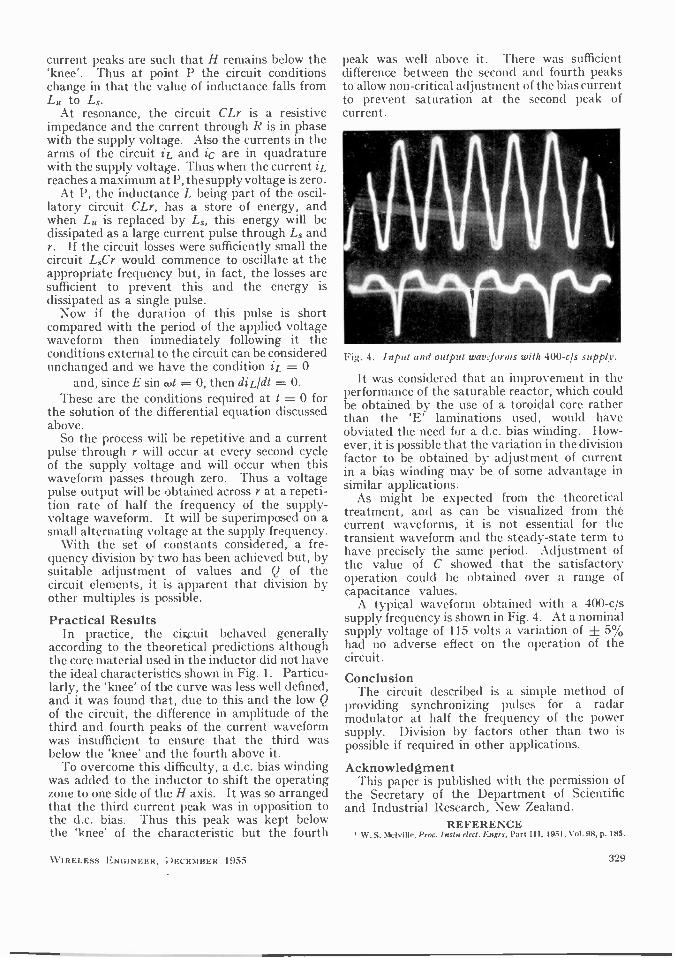
Fig. 4. Input and output wauf orms with 400-c/s supply.
It was considered that an improvement in the performance of the saturable reactor, which could be obtained by the use of a toroidal core rather than the 'E' laminations used, would have obviated the need for a d.c. bias winding. How- ever, it is possible that the variation in the division factor to be obtained by adjustment of current in a bias winding may be of some advantage in similar applications.
As might be expected from the theoretical treatment, and as can be visualized from tlié current \vaveforms, it is not essential for the transient waveform and the steady-state term to have precisely the same period. Adjustment of the value of C showed that the satisfactor\ operation could be obtained over a range of capacitance values.
A typical waveform obtained with a 400-c/s supply frequent\ is shown in Fig. 4. At a nominal supply voltage of 115 volts a variation of ± 5% had no adverse effect on the operation of the circuit.
Conclusion The circuit described is a simple method of
providing synchronizing pulses for a radar modulator at half the frequency of the power supply. Division by factors other than two is possible if required in other applications.
Acknowledgment This paper is published with the permission of
the Secretary of the Department of Scientific and Industrial Research, New Zealand.
REFERENCE W. S. Melville, Proc. lost' rlcct. I(grs, Part 1II, 1951. Vol.98, p. 185.
329
lit+Ldr_v+(T+RC)cv LC`-2 (1) dt dt dt
where R is the differential resistance of the tube C is the total capacitance of the tube L is a constant having the dimensions of
inductance T is a constant having the dimensions of
time.
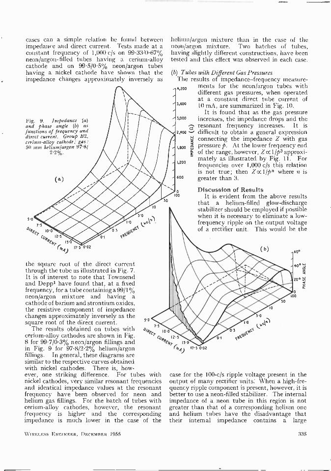
Fig. 5. Impedance (a) and phase -angle (b) as fnnc- tio as of frequency and direct current. Group A I, nickel cathode; gas: 40 min
neon 'argon 99'5/0'5%.
(a)
30
5'0 le 7'S` ./ ocAAcl
I 0' 0 ̀ / CoA 12'5 ` . 0'1
AFAT I50`I/ 6, 17'5 002
10
3'0
I Lyd,c.\zl
0 3 vVEy EP`
5.0
It should be noted here that according to this theory L is not associated with inertia effects. From equation (1) the admittance of a tube for small sinusoidal alternating currents of frequency f = to/27r superimposed on the steady current obtained as: -
1 + jwT R+jWL
The equivalent circuit of a glow -discharge tube is, therefore, not simply a resistor in series with an inductor, as is often assumed, but has a more complicated form as shown in Fig. 1. . The two circuit elements r = LIT and C' = T/R are introduced instead of simply the time constant T.
It should be borne in mind that C' is an imaginary capacitance only and may be infinite or even negative. C, which is associated with the actual capacitance of the tube, is always positive.
y- +jwC .
332
75 074>fCr 10'0
CUAAFNl2
5
150
(,gJ 17'5
Neglecting the capacitance oh the tube the impedance :-
R+jwL 1 + jwr
From this expression, as pointed out by van Geel, it is seen that :-
(1) The dynamic characteristic for very low frequencies is a straight line which coincides with
the static running-voltage/current curve of the tube (7 = R).
(2) For the intermediate -frequency range the dynamic characteristic is a small ellipse (7 is inductive) and
3,600 (3) For high frequencies the dynamic characteristic is again a straight line but with a different slope from the low - frequency characteristic (7 = L/T).
If the tube capacitance is taken into
3,000
2,400 account then it is found, from similar considerations, that the dynamic charac- teristic passes through all three stages mentioned above but becomes an ellipse again for very high frequencies and 7 is capacitive.
1,800
1,200
600
f
loó >_ (b)
is
.. (2)
4,200
0'02
lo
3'0
`µcsi
ii 0 3 OVa`y 01 EP`
(3)
60°
0°
-20°
It follows that some information about the differential impedance at low frequencies may be obtained from the form of the static running- voltage-current characteristic of the tube. For example, Fig. 2 shows that the static curves vary widely for tubes with different gas fillings, from which it is evident that at low frequencies the internal impedance of a helium -filled tube is much smaller than that of a neon tube. '1t high frequencies, however, the impedance depends mainly on the constants L and T and it may differ very much from the impedance observed at low frequencies.
The above theory has been verified by 'the
\\ IREL ESS ENGINEER, DECEMBER 1955
present measurements. A large number of different tubes have been tested and the im- pedance -frequency curves obtained are in com- plete agreement with the theory. This can be seen from the typical result of Fig. 3 showing the variations of resistance and reactance of a tube with frequency.
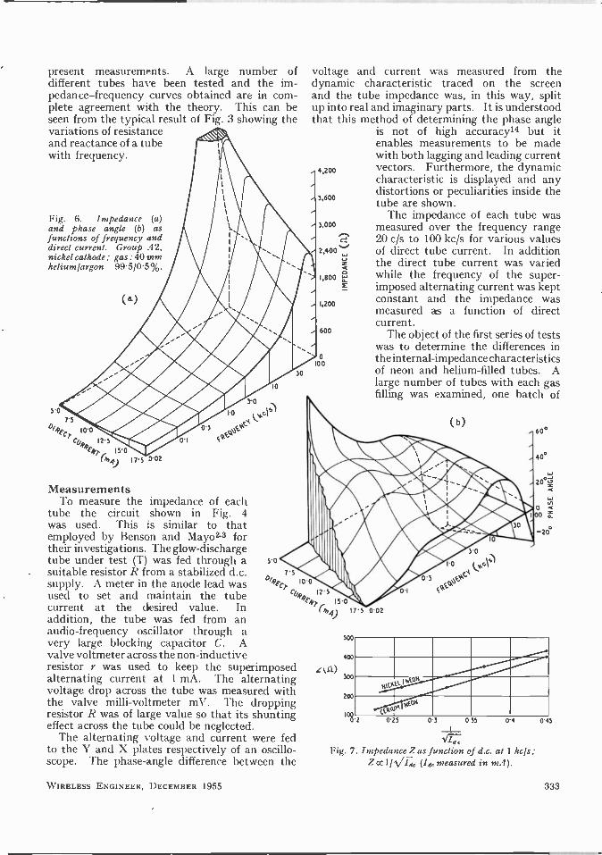
rig. 6. Impedance (a) and phase angle (b) as functions of frequency and direct current. Group .42, nickel cathode; gas: 40 mm helium/argon 99.5/0'5%.
5'0 75
a7qfcl 10'0
CUg 2 5
/ 1 a49 17.5 0102
(a)
0.1
10
3-0 I.0 lµclsl
0'3 aVEaC QE
Measurements To measure the impedance of each
tube the circuit shown in Fig. 4 was used. This is similar to that employed by Benson and Mayo2,3 for their investigations. The glow -discharge tube under test (T) was fed through a suitable resistor 1? from a stabilized d.c. supply. A meter in the anode lead was used to set and maintain the tube current at the desired value. In addition, the tube was fed from an audio -frequency oscillator through a very large blocking capacitor C. A valve voltmeter across the non -inductive resistor r was used to keep the superimposed alternating current at 1 mA. The alternating voltage drop across the tube was measured with the valve milli -voltmeter mV. The dropping resistor 1? was of large value so that its shunting effect across the tube could be neglected.
The alternating voltage and current were fed to the Y and X plates respectively of an oscillo- scope. The phase -angle difference between the
WIRELESS ENGINEER, DECEMBER 1955
5.0
7'5
'Elk" 10'0
2 5
6,4)17'5 0'02
voltage and current was measured from the dynamic characteristic traced on the screen and the tube impedance was, in this way, split up into real and imaginary parts. It is understood that this method of determining the phase angle
is not of high accuracy14 but it enables measurements to be made with both lagging and leading current
4,200 vectors. Furthermore, the dynamic characteristic is displayed and any distortions or peculiarities inside the tube are shown.
The impedance of each tube was 3,000 measured over the frequency range
20 c/s to 100 kc/s for various values 2,400 of direct tube current. In addition
= the direct tube current was varied while the frequency of the super- imposed alternating current was kept
1,200 constant and the impedance was measured as a function of direct current.
The object of the first series of tests was to determine the differences in
loó the internal -impedance characteristics of neon and helium -filled tubes. A large number of tubes with each gas filling was examined, one hatch of
vp.#14(b)
3,600
ó 1,800 f
600
«n)
500
400
300
200
log.2
0'I
0
I
i 0'3
y ENG
EQE
0°
40°
20°U Z
N o 00
-20
N\EKEL 1
NEON
0,INEON 0.25 03 035 04
J7, Fig. 7. Impedance Zas function of d.c. al 1 kc/s;
Zccl/VI7k (I,k measured in mA).
0'45
333
tubes having nickel cathodes, another cerium - alloy cathodes.
The second series of tests was concerned with the influence of gas pressure on the impedance. For this purpose a number of tubes containing a 99.33;0.67% neon/argon mixture was examined. Tubes were made having gas pressures of 30, 35, 40, 45 and 50 mm of mercury.
Experimental Results (a) Tubes with Different Gas Fillings
The mean results of the measurements on tubes
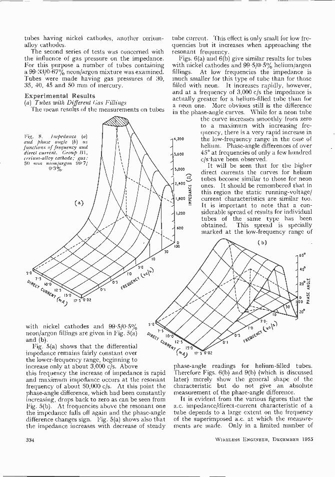
Fig. S. Impedance (a) and phase angle (b) as functions of frequency and direct current. Group Ill, cerium -alloy cathode; gas: 50 nun neon 'argon 99.7/
0'3%.
( a)
with nickel cathodes and 99.5/0.5% neon/argon fillings are given in Fig. 5(a) and (b).
Fig. 5(a) shows that the differential impedance remains fairly constant over the lower -frequency range, beginning to increase only at about 3,000 c/s. Above this frequency the increase of impedance is rapid and maximum impedance occurs at the resonant frequency of about 50,000 c/s. At this point the phase -angle difference, which had been constantly increasing, drops back to zero as can be seen from Fig. 5(b). At frequencies above the resonant one the impedance falls off again and the phase -angle difference changes sign. Fig. 5(a) shows also that the impedance increases with decrease of steady
334
tube current. This effect is only small for low fre- quencies but it increases when approaching the resonant frequency.
Figs. 6(a) and 6(h) give similar results for tubes with nickel cathodes and 99.5/0.5% helium/argon fillings. At low frequencies the impedance is much smaller for this type of tube than for those filled with neon. It increases rapidly, however, and at a frequency of 3,000 c/s the impedance is actually greater for a helium -filled tube than for a neon one. More obvious still is the difference in the phase -angle curves. While for a neon tube
the curve increases smoothly from zero to a maximum with increasing fre- quency, there is a very rapid increase in
4,200 the low -frequency range in the case of helium. Phase -angle differences of over
3,600 45° at frequencies of only a few hundred c/s-have been observed.
It will be seen that for the higher 3,000 direct currents the curves for helium
tubes become similar to those for neon 2 400 ones. It should be remembered that in
this region the static running -voltage/ 1,e00 á current characteristics are similar too.
It is important to note that a con - I,200 siderable spread of results for individual
tubes of the same type has been
600 obtained. This spread is specially marked at the low -frequency range of
phase -angle readings for helium -filled tubes. Therefore Figs. 6(b) and 9(b) (which is discussed later) merely show the general shape of the characteristic but do not give an absolute measurement of the phase -angle difference.
It is evident from the various figures that the a.c. impedance/direct-current characteristic of a tube depends to a large extent on the frequency of the superimposed a.c. at which the measure- ments are made. Only in a limited number of
WIRELESS ENGINEER, DECEhI13ER 1955
cases can a simple relation he found between impedance and direct current. Tests made at a constant frequency of 1,000 c/s on 99.33,0.67% neon/argon- filled tubes having a cerium -alloy cathode and on 99.5/0.5% neon/argon tubes having a nickel cathode have shown that the impedance changes approximately inversely as
Fig. 9. Impedance ja) and phase angle (b) as functions of frequency and direct current. Group B2, cerium -alloy cathode; gas: 50 nun helium 'argon 97.8/
2.2
(a)
#41111 ` 4 5-0
5 1.0
/ G`S
10'0 0 } pJaGi
C04'12'5 0'1 FPE
*1-4,7, 150/ 6,)I7-5
0'02
the square root of the direct current through the tube as illustrated in Fig. 7. It is of interest to note that Townsend and Deppl have found that, at a fixed frequency, for a tube containing a 99/1 % neon /argon mixture and having a cathode of barium and strontium oxides, the resistiv e component of impedance changes approximately inversely as the square root of the direct current.
The results obtained on tubes with cerium -alloy cathodes are shown in Fig. 8 for 99.7 0.3% neon/argon fillings and in Fig. 9 for 97.8/2.2% helium; argon fillings. In general, these diagrams are similar to the respective curves obtained with nickel cathodes. There is, how- ever, one striking difference. For tubes with nickel cathodes, very similar resonant frequencies and identical impedance values at the resonant frequency have been observed for neon and helium gas fillings. For the batch of tubes with cerium -alloy cathodes, however, the resonant frequency is higher and the corresponding impedance is much lower in the case of the
\VIHALIdSS ENGINEER, DECEMBER 1955
5.0
7'5 O/qfCr 10.0
helium/argon mixture than in the case of the neon/argon mixture. Two batches of tubes, having slightly different constructions, have been tested and this effect was observed in each case.
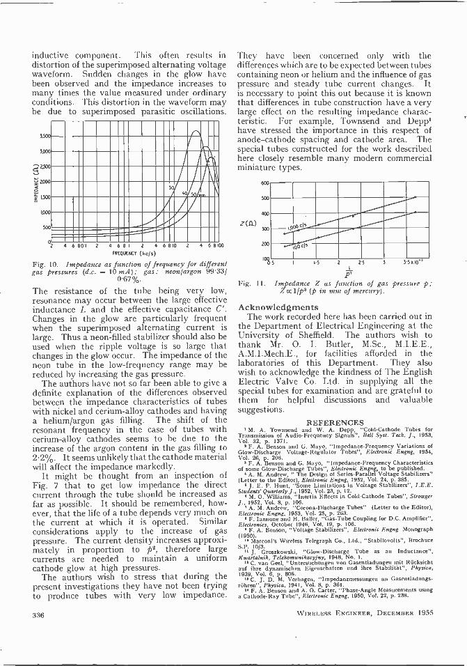
(b) Tubes with Different Gas Pressures The results of impedance-frequency measure - 4,200
ments for the neon/argon tubes with different gas pressures, when operated at a constant direct tube current of
3,600 10 mA, are summarized in Fig. 10. It is found that as the gas pressure
3,000 increases, the impedance drops and the resonant frequency increases. It is
2,400 difficult to obtain a general expression connecting the impedance Z with gas
1,800 W pressure p. At the lower frequency end of the range, however, Zoe 1
p3 approxi- mately as illustrated by Fig. 11. For frequencies over 1,000 c/s this relation is not true; then Zccl/m where n is greater than 3.
1,200
600
o Discussion of Results 100 It is evident from the above results
that a helium -filled glow -discharge stabilizer should be employed if possible when it is necessary to eliminate a low - frequency ripple on the output voltage of a rectifier unit. This would be the
rq) 15'0
17'5 0'02
0.1
(b)
1'0 K
0 '3 exc.; EP<pV
10
30
60°
40°
20° a
o loo
case for the 100-c/s ripple voltage present in the output of many rectifier units: \\hen a high -fre- quency ripple component is present, however, it is better to use a neon -filled stabilizer. The internal impedance of a neon tube in this region is not greater than that of a corresponding helium one and helium tubes have the disadvantage that their internal impedance contains a large
335
inductive component. This often results in distortion of the superimposed alternating voltage waveform. Sudden changes in the glow have been observed and the impedance increases to many times the value measured under ordinary conditions. This distortion in the waveform may be due to superimposed parasitic oscillations.
3.500
2,500
2000
0 1500
1.000
500
02 4 680'1 2 4 6 8 2 4 6810 2 4 68100
FR QUENCY (kc/s)
Fig. 10. Impedance as f tnction of frequency for different gas pressures (d.c. = 10 rnA); gas: neon/argon 99.33/
0.67%.
The resistance of the tube being very low, resonance may occur between the large effective inductance L and the effective capacitance C'. Changes in the glow are particularly frequent when the superimposed alternating current is large. Thus a neon -filled stabilizer should also be used when the ripple voltage is so large that changes in the glow occur. The impedance of the neon tube in the low -frequency range may be reduced by increasing the gas pressure.
The authors have not so far been able to give a definite explanation of the differences observed between the impedance characteristics of tubes with nickel and cerium -alloy cathodes and having a helium/argon gas filling. The shift of the resonant frequency in the case of tubes with cerium -alloy cathodes seems to be due to the increase of the argon content in the gas filling to 2.2%. It seems unlikely that the cathode material will affect the impedance markedly.
It might be thought from an inspection of Fig. 7 that to get low impedance the direct current through the tube should be increased as far as possible. It should be remembered, how- ever, that the life of a tube depends very much on the current at which it is operated. Similar considerations apply to the increase of gas pressure. The current density increases approxi- mately in proportion to p2, therefore large currents are needed to maintain a uniform cathode glow at high pressures.
The authors wish to stress that during the present investigations they have not been trying to produce tubes with very low impedance.
336
They have been concerned only with the differences which are to be expected between tubes containing neon or helium and the influence of gas pressure and steady tube current changes. It is necessary to point this out because it is known that differences in tube construction have a very large effect on the resulting impedance charac- teristic. For example, Townsend and Deppl have stressed the importance in this respect of anode-cathode spacing and cathode area. The special tubes constructed for the work described here closely resemble many modern commercial miniature types.
600
500
Z(1L)
400
300
200
05
1p00cs
--Too cis
15 2 25
Fig. 11. Impedance Z as function of gas pressure p; Z oc l/p3 (p in mm of mercury).
3 35210'
Acknowledgments The work recorded here has been carried out in
the Department of Electrical Engineering at the University of Sheffield. The authors wish to thank Mr. O. I. Butler, M.Sc., M.I.E.E., A.M.I.Mech.E., for facilities afforded in the laboratories of this Department. They also wish to acknowledge the kindness of The English Electric Valve Co. Ltd. in supplying all the special tubes for examination and are grateful to them for helpful discussions and valuable suggestions.
REFERENCES M. A. "rownsend and W. A. Depp, "Cold -Cathode Tubes for
Transmission of Audio -Frequency Signals", Bell Sysl. Tech. J., 1953, Vol. 32, p. 1371.
F. A. Benson and G. Mayo, "Impedance -Frequency Variations of Glow -Discharge Voltage -Regulator Tubes", Electronic Engng, 1954, Vol. 26, p. 206.
P. A. Benson and G. Mayo, "Impedance -Frequency Characteristics of some Glow -Discharge Tubes", Electronic Engng, to be published.
A. M. Andrew, " The Design of Series -Parallel Voltage Stabilizers" (Letter to the Editor), Electronic Engng, 1952, Vol. 24, p. 385.
3 J. E. P. Hunt, "Some Limitations in Voltage Stabilizers", I.E.E. Students' Quarterly J., 1952, Vol. 23, p. 12.
° 3I. O. Williams, "Inertia Effects in Cold -Cathode Tubes", Sfrowger J., 1952, Vol. 8, p. 106.
A. M. Andrew, "Corona -Discharge Tubes" (Letter to the Editor), Electronic Engng, 1953, Vol. 25, p. 263.
° F. lannone and H. Bailer, "Gas -Tube Coupling for D.C. Amplifier", Electronics, October 1946, Vol. 19, p. 106.
' F. A. Benson, "Voltage Stabilizers", Electronic Engng Monograph (1950).
10 Marconi's Wireless Telegraph Co., Ltd., "Stabilovolts", Brochure S.P. 10/3.
' J. Groszkowski, "Glow -Discharge Tube as an Inductance", Kwartalnik, Telekomunikacyjny, 1948, No. I. " C. van Geel, "Untersuchungen von Gasentladungen mit Rücksicht
auf ihre dynamischen Eigenschaf ten and ihre Stabilitüt", Physica, 1939, Vol. 6, p. 806.
13 C. J. D. M. V'erhagen, " Impedanzmessungen an Gasentladungs- rühren", Physica, 1941, Vol. 8, p. 361.
" F. A. Benson and A. O. Carter, "Phase -Angle Measurements using a Cathode -Ray Tube", Electronic Engng, 1950, Vol. 22, p. 238.
\VIREI.ESS ENGINEER, DECEMIOER 1955
CORRESPONDENCE Letters to the Editor on technical subjects are always welcome. In publishing such communications the Editors do not necessarily endorse any technical or general statements which they may contain.
A.M.-F.M. Demodulator SIR,-A new method of demodulation has been
developed by utilizing the rise -time characteristic of a pulse of constant amplitude obtained by properly limiting an amplitude- or a frequency -modulated wave.
Trapezoidal pulses of equal amplitude are produced when a sinusoidal wave is limited near the zero axis. The slope of the leading and the trailing edges of these pulses is essentially constant and is a linear function of the amplitude and the frequency of the sinusoidal wave. If a carrier is modulated either in amplitude or in frequency with a modulating signal (the time period of the latter being very long compared to that of the carrier) and is limited so as to select a small slicing level near the zero axis, trapezoidal pulses are produced. Here the slope of both edges of a particular pulse is constant, while for the succeeding pulses the slope varies proportionately according to the variation of amplitude of the modulating signal. It may he stated more clearly that the slope varies according to the instantaneous amplitude of the amplitude -modulated wave, or accord- ing to the instantaneous frequency of the frequency - modulated wave as shown in Fig. I (a) and (h) respectively.
A modulated wave (either a.nl. or Lin.) is thus trans- lated into slope -modulated trapezoidal pulses. On differentiating these pulses by means of a low time - constant CH circuit they arc converted into variable amplitude pulses on both sides of the axis, the amplitude of the differentiated pulses being proportional to the slope of the trapezoidal pulses. These a.m. pulses are then detected and passed through a pulse -lengthener circuit followed by an 1.f. filter to recover the modulating signal.
MODULATING VOLTAGE TIME
MODULATION ENVELOPE"
;, ^ Ii
LIMITING LEVEL
MODULATING VOLTAGE-, TIME FREQUENCY
MODULATED WAVE`
(a)
(b)
LIMITING LEVEL i ¡;;y; ¿ \," \i , y'
Fig. 1.
The block schematic diagram shown in Fig. 2 illustrates the circuit arrangement used to demodulate a carrier of 100 l:c¡s modulated by a 400 -cis tone. The modulated wave is first passed through a double -diode clipper followed by a cathode -follower differentiator. The differentiated output is then passed through a detector having an RC load with proper time constant, across which the modulating voltage is obtained and is observed on a c.r. oscilloscope. The system in itself, though less sensitive, is not more complicated than that of a con- ventional f.m. system. Although the number of operations to he performed on the waveform seem
WIRELESS i'.NGINFER, 1)Ecl=.nmER 1955
numerous they may he carried out quite simply. 1\lore- over, it eliminates the difficulty of aligning and provides a common system for the reception of both a.m. and f.m. waves.
MODULATED INPUT
CLIPPER DIFFERENTIATOR - DETECTOR 8 FILTER
Fig. 2.
The possibility of this system for noise reduction is under invest'gation. It may, however, be mentioned that the spurious noise in between the translated a.m. pulses may be eliminated by using a properly -biased gating circuit.
P. IíuNnc Indian Institute of "Technology, Iihargpur, India.
17th October 1955.
Rectifier -Filter Characteristics SIR, -I have only recently discovered a paper by
Professor E. B. \Ioullin (/. Instn elect. Engrs, 1937, Vol. 80, p. 553) in which lie uses an approach to rectifiers which is substantially the same as that presented in my paper on " Rectifier -Filter Characteristics", Wireless Engineer, June 1955, p.147. \Vhen I presented my paper for publication I was not aware of Professor Dloullin's paper and I am surprised that his approach to the problem has never received much attention.
The letter by Di. V. Joyce which you published in the September issue of Wireless Engineer is very interesting and I think that the criterion advocated by Mr. Joyce is a better one than the one I proposed in my paper. I should, however, prefer to be somewhat more conservative and set the following limits for reasonable prediction of capacitor input filter characteristics:-
27rfCr > 4 for half -wave rectification, 24-Cr > 2 for full -wave rectification.
F. C. FIEYNIANN University of the Witwatersrand,
Johannesburg, South Africa. 21st October 1955.
PREMIUMS FOR TECHNICAL WRITING The Radio Industry Council is prepared to award up
to six premiums of 25 guineas to the writers of articles published during the year which "are likely to enhance the reputation of the Industry and focus attention of peoples throughout the world on Britain's leadership in the fields of radio, television and electronics".
A leaflet describing the scheme and defining the eligibility of writers is obtainable from the Radio Industry Council, 59 Russell Square, London, W.C.I. This year's entries should be made prior to 31st December to the Secretary at the same address.
BRITISH STANDARDS INSTITUTION The British Standards institution has opened a
Sales Office in Birmingham at which a stock of British Standards and associated publications will be maintained. It is at the headquarters of the Chamber of Commerce, 95 New Street, Birmingham 2.
337
NEW BOOKS Transistors and Other Crystal Valves
By T. R. SCOTT, D.F.C., B.Sc., M.I.E.E., A.M.Inst.Pet. Pp. 258 + xvi. Macdonald & Evans Ltd., 8 John Street, Bedford Row, London, W.C.1. Price 45s.
The main concern of this book is with the 'internals' of the transistor and the crystal diode. Applications and circuits arc not treated at all fully. The book is not intended for the transistor designer, however, but for the user and its purpose is to tell him something of how they work.
Following the introduction, there is a chapter on crystal imperfections, in which it is shown that the imperfections are necessary for conduction in semi- conductor materials. Chapter 3 deals with the theory of p -n junctions and the design of junction diodes and transistors. Chapter 4 covers point -contact devices and Chapter 5 deals with operating temperature and its 'effect upon output and life.
There is a chapter covering applications, circuitry and testing and one dealing with special h.f. transistors. Appendixes treat the band structure of semiconductors and testing techniques. There is an extensive biblio- graphy.
The book is, to a large extent, non -mathematical. In spite of this, it is by no means easy reading, but that is to be expected from the nature of the subject. It should form a useful introduction to the subject for the reader having a good general background of physics.
W. T. C. Repairing Record Changers
By E. EUGENE ECKLUND. Pp. 278 + ix. McGraw- Hill Publishing Co., Ltd., 95 Farringdon Street, London, E.C.4. Price 44s. 6d.
British Standards Institution Annual Report 1954-55
Pp. 243. British Standards Institution, 2 Park Street, London, \V.1. Price 5s.
Wireless World Diary 1956 Consequent upon recent changes in purchase tax, the
price of the Wireless World Diary has been increased to 4s. 21d. in rexine and 6s. in leather (postage 2d. extra). Including pp. 79 of reference material and pp. 2 per week diary, it is available from Iliffe & Sons Ltd., Dorset House, Stamford Street, London, S.E.1.
Investigation of Deterioration of Moulded Carbon Resistors
By H. F. CHURCH and J. J. WALSH. First Report: Z/T92, pp. 28. Price 7s. 6d. Second Report: Z/T 96, pp. 23. Price 12s. 6d.
The Performance of Insulated Carbon -Resin Film Resistors
By F. G. RIVERS. Z/T 95, pp. 13. Price 15s. The above three reports can be obtained from the
Electrical Research Association, Thorncroft Manor, Dorking Road, Leatherhead, Surrey.
TECHNICAL LITERATURE Mullard Ferroxcube
Pp. 130. \Iullard Ltd., Components Division, Century House, Shaftesbury Avenue, London, W.C.2. Price 7s. 6d.
This book contains technical information on the properties and application of Ferroxcube. The main sections cover magnetic ferrites, types and grades of Ferroxcube, mechanical properties, electrical and magnetic properties, applications, rectangular B -H loop material and standard core shapes and dimensions.
338
MEE'T'INGS I.E.E.
7th December. "Some Half -Tone Storage Tubes", by R. S. Webley, B.Sc., H. G. Lubczynski, Dr. Ing. and J. A. Lodge, B.Sc.
12th December. "The Television Studio as seen by the Producer", by Alvin Rakoff.
These meetings will he held at the Institution of Electrical Engineers, Savoy Place, Victoria Embank- ment, Loncfon, W.C.2 and will commence at 5.30.
Brit.I.R.E. 14th December. "The Remote Presentation of Radar
Information", by G. J. Dixon and H. H. Thomas, to be held at the London School of Hygiene and Tropical Medicine, Keppel Street, Gower Street, London, W.C.1, at 6.30.
The Television Society 9th December. "The Secondary Emission Valve and
its Applications", by A. H. Atherton, to be held at 7 o'clock at the Cinematograph Exhibitors' Association, 164 Shaftesbury Avenue, London, \\'.C.2.
STANDARD -FREQUENCY TRANSMISSIONS (Communication from the National Physical Laboratory)
Values for October 1955
Date 1955
October
Frequency deviation from nominal: parts in 108
MSF 60 kc/s 1429-1530 G.M.T.
Droitwich 200 kc/s
1030 G.M.T.
I +04 +2 2 +0.4 +3 3 +0.4 +2 4 N.M. +2 5 +0.4 +2 6 +0.5 +3 7 +0.5 +2 8 +0.5 +2 9 +0.5 +3 0 +0.5 +2
+0.4 , +3 2 I-0.5 +3 3 +0.4 +3 4 +0.3 +3 5 +0.4 +3 6 +0.5 +4 7 +0.5 +4 8 +0'S +4 9 +0.5 +4
20 +0.5 +4 21 +0.4 +4 22 +0.4 +4 23 +0.4 +4 24 +05 +4 25 +0.5 +3 26 +05 +3 27 -F-O'6 +5 28 +0.6 +5 29 I +0.6 +6 30 +0.6 +6 31 N.T. +6
The values are based on astronomical data available on 1st November 1955.
N.M. = Not Measured. N.T. = No Transmission.
WIRELESS ENGINEER, DECEMBER 1955


