Embed Size (px)
Citation preview

K19007
From power electronics to power integrated circuits (PICs), smart power technologies, devices, and beyond, Integrated Power Devices and TCAD Simulation provides a complete picture of the power management and semiconductor industry. An essential reference for power device engineering students and professionals, the book not only describes the physics inside integrated power semiconductor devices such lateral double-diffused metal oxide semiconductor field-effect transistors (LDMOSFETs), lateral insulated-gate bipolar transistors (LIGBTs), and super junction LDMOSFETs but also delivers a simple introduction to power management systems. Instead of abstract theoretical treatments and daunting equations, the text uses technology computer-aided design (TCAD) simulation examples to explain the design of integrated power semiconductor devices. It also explores next generation power devices such as gallium nitride power high electron mobility transistors (GaN power HEMTs).
Including a typical process flow for smart PIC technology as well as a hard-to-find technology development organization chart, Integrated Power Devices and TCAD Simulation gives students and junior engineers a head start in the field of power semiconduc-tor devices while helping to fill the gap between power device engineering and power management systems.
Electrical Engineering
Y u e F u • Z h a n m i n g L iW a i Tu n g N g • J o h n n y K . O . S i n
Integrated PowerDevices and TCAD
Simulation
Fu • Li
Ng • Sin
Integrated Power Devicesand TCAD Simulation
Integrated Power Devices and TCAD Sim
ulation

Integrated PowerDevices and TCAD
Simulation

Devices, Circuits, and Systems
Series Editor Krzysztof Iniewski
CMOS Emerging Technologies Research Inc., Vancouver, British Columbia, Canada
PUBLISHED TITLES:
Atomic Nanoscale Technology in the Nuclear IndustryTaeho Woo
Biological and Medical Sensor TechnologiesKrzysztof Iniewski
Building Sensor Networks: From Design to ApplicationsIoanis Nikolaidis and Krzysztof Iniewski
Circuits at the Nanoscale: Communications, Imaging, and SensingKrzysztof Iniewski
Electrical Solitons: Theory, Design, and Applications David Ricketts and Donhee Ham
Electronics for Radiation Detection Krzysztof Iniewski
Embedded and Networking Systems: Design, Software, and Implementation
Gul N. Khan and Krzysztof Iniewski
Energy Harvesting with Functional Materials and MicrosystemsMadhu Bhaskaran, Sharath Sriram, and Krzysztof Iniewski
Graphene, Carbon Nanotubes, and Nanostuctures: Techniques and Applications
James E. Morris and Krzysztof Iniewski
High-Speed Photonics InterconnectsLukas Chrostowski and Krzysztof Iniewski
Integrated Microsystems: Electronics, Photonics, and Biotechnology Krzysztof Iniewski
Integrated Power Devices and TCAD SimulationYue Fu, Zhanming Li, Wai Tung Ng, and Johnny K.O. Sin
Internet Networks: Wired, Wireless, and Optical TechnologiesKrzysztof Iniewski
Low Power Emerging Wireless TechnologiesReza Mahmoudi and Krzysztof Iniewski
Medical Imaging: Technology and ApplicationsTroy Farncombe and Krzysztof Iniewski

CRC Press is an imprint of theTaylor & Francis Group, an informa business
Boca Raton London New York
Yu e F u • Z h a n m i n g L iWa i Tu n g N g • J o h n n y K . O . S i n
Integrated PowerDevices and TCAD
Simulation

CRC PressTaylor & Francis Group6000 Broken Sound Parkway NW, Suite 300Boca Raton, FL 33487-2742
© 2014 by Taylor & Francis Group, LLCCRC Press is an imprint of Taylor & Francis Group, an Informa business
No claim to original U.S. Government worksVersion Date: 20131119
International Standard Book Number-13: 978-1-4665-8383-2 (eBook - PDF)
This book contains information obtained from authentic and highly regarded sources. Reasonable efforts have been made to publish reliable data and information, but the author and publisher cannot assume responsibility for the valid-ity of all materials or the consequences of their use. The authors and publishers have attempted to trace the copyright holders of all material reproduced in this publication and apologize to copyright holders if permission to publish in this form has not been obtained. If any copyright material has not been acknowledged please write and let us know so we may rectify in any future reprint.
Except as permitted under U.S. Copyright Law, no part of this book may be reprinted, reproduced, transmitted, or uti-lized in any form by any electronic, mechanical, or other means, now known or hereafter invented, including photocopy-ing, microfilming, and recording, or in any information storage or retrieval system, without written permission from the publishers.
For permission to photocopy or use material electronically from this work, please access www.copyright.com (http://www.copyright.com/) or contact the Copyright Clearance Center, Inc. (CCC), 222 Rosewood Drive, Danvers, MA 01923, 978-750-8400. CCC is a not-for-profit organization that provides licenses and registration for a variety of users. For organizations that have been granted a photocopy license by the CCC, a separate system of payment has been arranged.
Trademark Notice: Product or corporate names may be trademarks or registered trademarks, and are used only for identification and explanation without intent to infringe.
Visit the Taylor & Francis Web site athttp://www.taylorandfrancis.com
and the CRC Press Web site athttp://www.crcpress.com

We would like to thank our family members
Holly Li, Angelina Fu, Vivian Zhou, Wailyn Chung, Casey Ng, Erin Ng, Susan Ho, Andrea Sin, and Benjamin Sin
for their understanding and support.


vii
ContentsPreface..............................................................................................................................................xvAbout the Authors ..........................................................................................................................xvii
Chapter 1 Power Electronics, the Enabling Green Technology ....................................................1
1.1 Introduction to Power Electronics .....................................................................11.2 History of Power Electronics .............................................................................31.3 DC/DC Converters ............................................................................................41.4 Linear Voltage Regulators .................................................................................41.5 Switched Capacitor DC/DC Converters (Charge Pumps) .................................51.6 Switched Mode DC/DC Converters ..................................................................71.7 Comparison between Linear Regulators, Charge Pumps, and Switched
Regulators ..........................................................................................................81.8 Topologies for Nonisolated DC/DC Switched Converters ................................9
1.8.1 Buck Converter .....................................................................................91.8.2 Boost Converter .................................................................................. 111.8.3 Buck–Boost Converter........................................................................ 131.8.4 Ćuk Converter .................................................................................... 141.8.5 Additional Topics in Nonisolated Converters .................................... 15
1.8.5.1 Nonideal Power Elements ................................................... 151.8.5.2 Synchronous Rectification .................................................. 151.8.5.3 Continuous Conduction Mode (CCM) and
Discontinuous Conduction Mode (DCM) .......................... 161.8.5.4 Interleaving ......................................................................... 161.8.5.5 Ripples ................................................................................ 161.8.5.6 Comparison of Nonisolated Topologies.............................. 16
1.9 Topologies for Isolated Switching Converters ................................................. 171.9.1 Flyback Converters ............................................................................. 171.9.2 Forward Converters ............................................................................ 181.9.3 Full-Bridge Converters ....................................................................... 191.9.4 Half-Bridge Converters ...................................................................... 211.9.5 Push–Pull Converters ......................................................................... 211.9.6 Additional Topics in Isolated DC/DC Converters ..............................22
1.9.6.1 Synchronous Rectification of Isolated DC/DC Converters ....221.9.6.2 Power MOSFET Parallel Body Diode Conduction ............221.9.6.3 Transformer Utilization ......................................................231.9.6.4 Voltage Stress on the Active Power Transistor ...................23
1.9.7 Comparison of Isolated DC/DC Converter Topologies .....................241.10 SPICE Circuit Simulation ................................................................................241.11 Power Management Systems for Battery-Powered Devices ............................251.12 Summary .........................................................................................................26
Chapter 2 Power Converters and Power Management ICs .........................................................27
2.1 Dynamic Voltage Scaling for VLSI Power Management ................................27

viii Contents
2.2 Integrated DC/DC Converters .........................................................................292.2.1 Segmented Output Stage .................................................................... 312.2.2 Transient Suppression with an Auxiliary Stage .................................34
2.3 Summary ......................................................................................................... 38
Chapter 3 Semiconductor Industry and More than Moore ......................................................... 39
3.1 Semiconductor Industry .................................................................................. 393.2 History of the Semiconductor Industry ........................................................... 39
3.2.1 A Brief Timeline ................................................................................ 393.2.2 The Traitorous Eight .......................................................................... 393.2.3 Historical Road Map of the Semiconductor Industry ........................ 39
3.3 Food Chain Pyramid of the Semiconductor Industry ..................................... 423.3.1 Level 1: Wafer and EDA Tools ........................................................... 423.3.2 Level 2: Device Engineering .............................................................. 433.3.3 Level 3: IC Design ..............................................................................443.3.4 Level 4: Manufacturing, Packaging, and Testing ...............................443.3.5 Level 5: Systems and Software .......................................................... 453.3.6 Level 6: Marketing and Sales ............................................................. 45
3.4 Semiconductor Companies ..............................................................................463.5 More than Moore ............................................................................................. 47
Chapter 4 Smart Power IC Technology....................................................................................... 51
4.1 Smart Power IC Technology Basics ................................................................ 514.2 Smart Power IC Technology: Historical Perspective ...................................... 514.3 Smart Power IC Technology: Industrial Perspective .......................................54
4.3.1 Engineering Groups of a Smart Power IC Technology ......................544.3.1.1 Process Integration .............................................................544.3.1.2 TCAD Support .................................................................... 554.3.1.3 Compact Modeling ............................................................. 554.3.1.4 Device Design ..................................................................... 554.3.1.5 ESD Design ........................................................................ 554.3.1.6 Process Design Kit .............................................................564.3.1.7 IC Design Group .................................................................564.3.1.8 Reliability Group ................................................................564.3.1.9 Packaging ............................................................................ 56
4.3.2 Smart Power IC Technology Development Flow ...............................564.3.3 Planning Stage .................................................................................... 564.3.4 Process Integration and Device Design ............................................. 574.3.5 Layout, Tape-Out, Fabrication, and Test ............................................604.3.6 Reliability and Qualification ..............................................................604.3.7 Survey of Current Smart Power Technology ..................................... 61
4.4 Smart Power IC Technology: Technological Perspective ................................ 624.4.1 Devices for Smart Power Technology ................................................ 624.4.2 Design Considerations for Smart Power IC Technology .................... 63
4.4.2.1 Power MOSFETs ................................................................ 634.4.2.2 LIGBTs ...............................................................................644.4.2.3 Analog Active Devices .......................................................644.4.2.4 Resistors ..............................................................................654.4.2.5 Capacitors ...........................................................................65

ixContents
4.4.2.6 Voltage and Frequency Trims .............................................654.4.2.7 Logic/Digital NMOS and PMOS .......................................654.4.2.8 System-Level Design and Fabrication Considerations .......65
4.4.3 Isolation Methods ...............................................................................66
Chapter 5 Introduction to TCAD Process Simulation ................................................................ 67
5.1 Overview ......................................................................................................... 675.2 Mesh Setup and Initialization .......................................................................... 675.3 Ion Implantation ..............................................................................................69
5.3.1 Analytical Models ..............................................................................695.3.2 Multiple-Layer Implantation .............................................................. 705.3.3 Monte Carlo Simulation ..................................................................... 70
5.4 Deposition ........................................................................................................ 725.5 Oxidation ......................................................................................................... 72
5.5.1 Dry Oxidation .................................................................................... 735.5.2 Wet Oxidation .................................................................................... 735.5.3 Oxidation Models ............................................................................... 73
5.5.3.1 Moving Boundaries ............................................................ 735.5.3.2 2D Analytical Models ......................................................... 745.5.3.3 Numerical Models .............................................................. 745.5.3.4 LOCOS Growth Example ................................................... 75
5.6 Etching ............................................................................................................. 755.7 Diffusion ..........................................................................................................77
5.7.1 Diffusion Mechanisms .......................................................................775.7.1.1 Direct Diffusion Mechanism ..............................................775.7.1.2 Vacancy Mechanism ...........................................................775.7.1.3 Interstitials Mechanism ......................................................77
5.7.2 Diffusion Models ................................................................................ 785.7.2.1 Fermi Diffusion Model ....................................................... 785.7.2.2 Two-Dimensional Diffusion Model .................................... 785.7.2.3 Fully Coupled Diffusion Model .......................................... 785.7.2.4 Steady-State Diffusion Model ............................................ 795.7.2.5 Oxide Enhanced (Retarded) Diffusion ............................... 79
5.8 Segregation ......................................................................................................805.9 Process Simulator Models Calibration ............................................................ 825.10 Introduction to 3D TCAD Process Simulation ................................................ 825.11 GPU Simulation ...............................................................................................84
Chapter 6 Introduction to TCAD Device Simulation .................................................................87
6.1 Overview .........................................................................................................876.2 Basics about Device Simulation ......................................................................87
6.2.1 Drift-Diffusion Model ........................................................................876.2.2 Discretization .....................................................................................876.2.3 Newton’s Method................................................................................886.2.4 Initial Guess and Adaptive Bias Stepping .......................................... 896.2.5 Convergence Issues ............................................................................906.2.6 Boundary Conditions ......................................................................... 91
6.2.6.1 Ohmic Contact .................................................................... 916.2.6.2 Schottky Contacts ............................................................... 91

x Contents
6.2.6.3 Neumann Boundaries .........................................................926.2.6.4 Lumped Elements ...............................................................926.2.7 Transient Simulation ...........................................................92
6.2.8 Mesh Issues ........................................................................................936.3 Physical Models ...............................................................................................93
6.3.1 Carrier Statistics .................................................................................936.3.2 Incomplete Ionization of Impurities ...................................................936.3.3 Heavy Doping Effect ..........................................................................946.3.4 SRH and Auger Recombination .........................................................946.3.5 Avalanche Breakdown and Impact Ionization ...................................94
6.3.5.1 Avalanche Breakdown ........................................................946.3.5.2 Impact Ionization Coefficients ............................................956.3.5.3 Chynoweth’s Law ................................................................956.3.5.4 Baraff Model .......................................................................966.3.5.5 Fulop’s Approximation .......................................................966.3.5.6 Okuto–Crowell Model ........................................................966.3.5.7 Lackner Model ....................................................................966.3.5.8 Mean Free Path Model .......................................................976.3.5.9 Multiplication Factor and Ionization Integral .....................986.3.5.10 Critical Electric Field ..........................................................996.3.5.11 Analytical Breakdown Voltage ......................................... 1006.3.5.12 Benchmark Comparison of Avalanche Breakdown
Models .............................................................................. 1006.3.6 Carrier Mobility ............................................................................... 100
6.3.6.1 Models Overview .............................................................. 1016.3.6.2 Constant Mobility ............................................................. 1016.3.6.3 Two-Piece Mobility Model ............................................... 1026.3.6.4 Canali or Beta Model ........................................................ 1026.3.6.5 Transferred Electron Model .............................................. 1026.3.6.6 Poole–Frenkel Field Enhanced Mobility Model .............. 1026.3.6.7 Impurity Dependence of the Low Field Mobility Model ....1036.3.6.8 Intel’s Local Field Models ................................................ 1036.3.6.9 Lombardi Model ............................................................... 1036.3.6.10 Comparison of Different Diffusion Models ..................... 1046.3.6.11 GaN Mobility Model (MTE Model) ................................. 104
6.3.7 Thermal and Self-Heating ................................................................ 1066.3.7.1 Heat Flow and Temperature Distribution ......................... 106
6.3.8 Bandgap Narrowing Effect ............................................................... 1076.4 AC Analysis ................................................................................................... 108
6.4.1 Introduction ...................................................................................... 1086.4.2 Basic Formulas ................................................................................. 1086.4.3 AC Analysis in TCAD ..................................................................... 111
6.5 Trap Model in TCAD Simulation .................................................................. 1126.5.1 Trap-Charge States ........................................................................... 1126.5.2 Trap Dynamics ................................................................................. 112
6.6 Quantum Tunneling ....................................................................................... 1156.6.1 Importance of Quantum Tunneling for Power Devices ................... 1156.6.2 Basic Theory of Tunneling for TCAD Simulation ........................... 1166.6.3 Introduction to Nonequilibrium Green’s Function for Tunneling .... 119
6.7 Device Simulator Models Calibration ........................................................... 119

xiContents
Chapter 7 Power IC Process Flow with TCAD Simulation ...................................................... 121
7.1 Overview ....................................................................................................... 1217.2 A Mock-Up Power IC Process Flow .............................................................. 121
7.2.1 Process Flow Steps ........................................................................... 1217.2.2 Structure View of the Mock-Up Process Flow ................................. 121
7.3 Smart Power IC Process Flow Simulation .................................................... 1237.3.1 P+ Substrate ...................................................................................... 1237.3.2 N+ Buried Layer ............................................................................... 1237.3.3 Epitaxial Layer Growth and Deep N Link .......................................1247.3.4 High-Voltage Twin-Well ................................................................... 1277.3.5 P-Body Implant for n-LDMOS ......................................................... 1287.3.6 Active Area/Shallow Trench Isolation (STI) .................................... 1307.3.7 N-Well and P-Well ............................................................................ 1347.3.8 Low-Voltage Twin Wells .................................................................. 1367.3.9 Thick Gate and Thin Gate Oxide ..................................................... 1377.3.10 Poly Gate .......................................................................................... 1407.3.11 NLDD and PLDD............................................................................. 1427.3.12 Sidewall Spacer ................................................................................ 1437.3.13 NSD and PSD ................................................................................... 1447.3.14 Back-End of the Line ........................................................................ 146
Chapter 8 Integrated Power Semiconductor Devices with TCAD Simulation ......................... 153
8.1 PN Junction Diodes ....................................................................................... 1538.1.1 PN Junction Basics ........................................................................... 1538.1.2 Lateral PN Junction Diode at Equilibrium ....................................... 1548.1.3 Forward Conduction (On-State) ....................................................... 1578.1.4 Reverse Bias of a PN Junction Diode ............................................... 1598.1.5 Lateral PN Junction Diode with NBL .............................................. 1608.1.6 Breakdown Voltage Enhancement of the PN Junction Diode .......... 160
8.1.6.1 Basic Understanding of How to Improve Breakdown Voltage .............................................................................. 161
8.1.6.2 Different P-Substrate Doping for the PN Junction Diode without NBL .......................................................... 163
8.1.6.3 Breakdown Enhancement for Diode with NBL................ 1658.1.6.4 Reverse Leakage Current Path with Substrate Contact .... 168
8.1.7 Reverse Recovery ............................................................................. 1688.1.7.1 Basic Understanding of Diode Reverse Recovery ............ 1688.1.7.2 Diode Reverse Recovery TCAD Simulation .................... 1708.1.7.3 TCAD Simulations for Carrier Lifetime Engineering ..... 170
8.1.8 Schottky Diode ................................................................................. 1708.1.9 Zener Diode ...................................................................................... 1748.1.10 Small Signal Model for PN Junction Diode ..................................... 175
8.2 Bipolar Junction Transistors .......................................................................... 1778.2.1 Basic Operation of NPN BJTs .......................................................... 178
8.2.1.1 Simulation Structure ......................................................... 1788.2.1.2 Collector and Base Current .............................................. 1808.2.1.3 Transistor Gain and Gummel Plot .................................... 180
8.2.2 NPN BJT Breakdown ....................................................................... 1818.2.2.1 BVCBO ................................................................................ 181

xii Contents
8.2.2.2 BVEBO ................................................................................ 1818.2.2.3 BVCEO ................................................................................ 1818.2.2.4 BVCES................................................................................. 1838.2.2.5 Comparison of the Four Types of NPN Breakdown ......... 184
8.2.3 BJT I-V Family of Curves ................................................................ 1858.2.4 Kirk Effect ........................................................................................ 1868.2.5 BJT Thermal Runaway and Second Breakdown Simulation ........... 1878.2.6 BJT Small Signal Model and Cutoff Frequency Simulation ............ 192
8.2.6.1 Cutoff Frequency .............................................................. 1938.3 LDMOS ......................................................................................................... 193
8.3.1 Breakdown Voltage Improvement .................................................... 1948.3.1.1 Basic LDMOS Structure with N-Type Epitaxial Layer
(LDMOS I) ....................................................................... 1948.3.1.2 LDMOS with Shielding Plate (LDMOS II)...................... 1968.3.1.3 LDMOS with STI in the Drain-Drift Region (LDMOS
III) ..................................................................................... 2018.3.1.4 LDMOS with Both STI Oxide and Field Plate
(LDMOS IV) ....................................................................2038.3.1.5 LDMOS with RESURF from P-epi Layer (LDMOS V) ...2068.3.1.6 LDMOS with P-epi RESURF and STI (LDMOS VI)......2098.3.1.7 LDMOS with Double RESURF (LDMOS VII) ............... 2128.3.1.8 LDMOS Multiple RESURF (LDMOS VIII).................... 2188.3.1.9 Comparison of 3D Surface Plot of Electric Field ............. 221
8.3.2 Parasitic NPN BJTs in LDMOS ....................................................... 2218.3.3 LDMOS On-State Resistance........................................................... 223
8.3.3.1 Specific On-Resistance .....................................................2258.3.3.2 On-Resistance Contribution..............................................2258.3.3.3 Comparison of Breakdown Voltage and On-Resistance ... 226
8.3.4 LDMOS Threshold Voltage ............................................................. 2278.3.5 LDMOS with Radiation Hardening Design .....................................2288.3.6 LDMOS I-V Family of Curves ......................................................... 2298.3.7 LDMOS Self-Heating .......................................................................2308.3.8 LDMOS Parasitic Capacitances ....................................................... 2328.3.9 LDMOS Gate Charge .......................................................................2348.3.10 LDMOS Unclamped Inductive Switching (UIS) ............................. 2368.3.11 Compact Models of LDMOS ........................................................... 237
Chapter 9 Integrated Power Semiconductor Devices with 3D TCAD Simulations .................. 239
9.1 3D Device Layout Effect ............................................................................... 2399.2 3D Simulation of LIGBT ...............................................................................242
9.2.1 About LIGBT ...................................................................................2429.2.2 Segmented Anode LIGBT ................................................................ 2439.2.3 3D Process Simulation of Segmented Anode LIGBT ......................2459.2.4 3D Device Simulation of Segmented Anode LIGBT .......................248
9.2.4.1 Forward Characteristic Simulation ...................................2489.2.4.2 LIGBT Turnoff Transient Simulation ............................... 2519.2.4.3 Forward I-V Family of Curves Comparison with
LDMOS ............................................................................ 2539.3 Super Junction LDMOS ................................................................................254
9.3.1 Basic Concept ...................................................................................254

xiiiContents
9.3.1.1 How to Choose the Pillar Width WN ................................ 2559.3.1.2 About Dose Balance ......................................................... 2589.3.1.3 On-Resistance ...................................................................260
9.3.2 Super Junction LDMOS Structure ................................................... 2619.3.3 3D Process Simulation of Super Junction LDMOS ......................... 2639.3.4 3D Device Simulation of Super Junction LDMOS ..........................2649.3.5 3D Simulation of a Standard LDMOS with the Same N-Drift
Doping ..............................................................................................2649.3.6 3D Simulation of a Standard LDMOS with Reduced N-Drift
Doping ..............................................................................................2669.3.7 Comparison of Super Junction LDMOS and Standard LDMOS ..... 267
9.4 Super Junction Power FinFET .......................................................................2689.4.1 Process Flow of the Super Junction Power FinFET .........................2699.4.2 Measurement Results of Super Junction Power FinFET .................. 2709.4.3 3D Simulation of Super Junction Power FinFET ............................. 271
9.5 Large Interconnect Simulation ...................................................................... 2749.5.1 3D Process Simulation of the Large Interconnect ........................... 275
9.5.1.1 Substrate ........................................................................... 2769.5.1.2 Contacts ............................................................................ 2769.5.1.3 Metal1 ............................................................................... 2779.5.1.4 Via1 ................................................................................... 2779.5.1.5 Metal2 ............................................................................... 2779.5.1.6 Via2 ................................................................................... 2799.5.1.7 Metal3 ............................................................................... 279
9.5.2 3D Device Simulation of the Large Interconnect.............................280
Chapter 10 GaN Devices, an Introduction .................................................................................. 281
10.1 Compound Materials versus Silicon .............................................................. 28110.2 Substrate Materials for GaN Devices ............................................................ 28210.3 Polarization Properties of III-Nitride Wurtzite ............................................. 283
10.3.1 Microscopic Dipoles and Polarization Vector .................................. 28310.3.2 Crystal Structure and Polarization ...................................................28410.3.3 Ideal c0/a0 Ratio for Zero Net Polarization ......................................284
10.3.3.1 Strain-Induced Polarization ..............................................28510.3.3.2 Empirical Approach to Modeling Polarization ................286
10.4 AlGaN/GaN Heterojunction ..........................................................................28710.4.1 Band Diagram Plots with a Fixed Al Mole Fraction ........................28810.4.2 Band Diagram Plots with a Fixed AlGaN Thickness ...................... 28910.4.3 AlGaN/GaN Structure with Doped AlGaN or GaN Layer. ............. 28910.4.4 AlGaN/GaN Structure with Metal Contacts .................................... 291
10.5 Traps in AlGaN/GaN Structure .....................................................................29210.6 A Simple AlGaN/GaN HEMT ......................................................................294
10.6.1 Device Structure ...............................................................................29410.6.2 Id-Vg Curves for GaN HEMT ...........................................................29410.6.3 Summary .......................................................................................... 295
10.7 GaN Power HEMT Example I ......................................................................29710.7.1 Device Structure ...............................................................................29710.7.2 Impact Ionization Coefficient of GaN Material ...............................29710.7.3 Breakdown Simulation of GaN HEMT............................................299
10.8 GaN Power HEMT Example II .....................................................................300

xiv Contents
10.9 Gate Leakage Simulation of GaN HEMT ..................................................... 30110.9.1 Device Structure ............................................................................... 30110.9.2 Models and Simulation Setup........................................................... 30110.9.3 Gate Leakage Simulation .................................................................302
10.9.3.1 Pure TCAD Simulation ....................................................30210.9.3.2 TCAD Simulation with Slow Transient ............................30410.9.3.3 TCAD Simulation with Equivalent Circuits .....................304
10.10 Market Prospect of Compound Semiconductors for Power Applications .....305
Appendix A: Carrier Statistics ...................................................................................................307
Appendix B: Process Simulation Source Code .........................................................................309
Appendix C: Trap Dynamics and AC Analysis ........................................................................ 321
Bibliography ................................................................................................................................. 323

xv
PrefaceEver since the invention of the transistor in the late 1940s, the development of transistors followed in two major directions: device miniaturization and performance improvement. One of the key parameters for performance improvement is obviously the power rating of the transistor, with devel-opment that resulted in the area of power semiconductors. Because all electrical devices require a supply of power and power management electronics for proper operation, power semiconductors are an important area of transistor development over the past decades.
In recent years, device miniaturization has allowed the minimum feature size to approach the nanoscale, and present ultra-large scale integration (ULSI) technology is capable of putting billions of transistors onto a single chip. This causes serious problems in powering up the chips. Furthermore, higher power efficiency required due to environmental issues also puts a heavy burden on the power management and power electronics part of the system. These and other related issues spur continued research into the area of power semiconductor devices and technology.
In the area of power semiconductor development, the focus was first on discrete power devices for high-power ratings. Typical structures were power bipolar transistors and thyristors. Due to the slow switching speed and high switching loss of these devices, a fast switching device such as the vertical double-diffused MOS (VDMOS) transistor was invented, and finally for over-all lower power loss, the insulated-gate bipolar transistor (IGBT) was created. As integrated circuit (IC) technology became more popular, there was a push to integrate power transistors with control IC for low-cost, compact, and high-performance applications. To accomplish this, lateral double-diffused MOS (LDMOS) transistors and lateral insulated-gate bipolar transistors (LIGBTs) were developed. That was the golden age for the development of the power IC (PIC) technology, and various kinds of bipolar-CMOS-DMOS (BCD) technologies were developed.
With today’s well-developed ULSI and PIC technologies, it is envisaged that development of a power system-on-a-chip (PowerSOC) for future consumer and industrial applications will be a very promising direction. Of course, to make that a reality, various other technologies for achieving high-performance monolithic passive components such as efficient passive and IC integration and effective power dissipation will also be needed.
Both high-performance lateral power transistors and process technologies are necessary to develop PIC technologies. For efficient design of semiconductor devices and process technologies, technology computer-aided design (TCAD) tools are commonly used in the industry. Some books have already been published on power device design and technology development, but none particu-larly focus on how to use TCAD tools to design and develop power devices and PICs. It is the purpose of this book to cover this need and especially to give engineers who are new to the field of power semiconductors a quick start on device and technology design and development using TCAD tools.
The book adopts a top-down approach to introduce new engineers to the field. It begins with basic power electronics systems and an introduction to power ICs and guides the reader to explore the semiconductor industry before getting into smart power IC technology. It then goes on to explain the basics of TCAD modeling for process and device simulation. Model calibration for specific fab-rication facilities for accurate and reliable simulation results are also discussed. Details on how to use TCAD tools for power IC process development and power device designs are then introduced. This includes many simulation examples on TCAD methodology and procedures for industrial design of practical power devices and process technologies. More than 300 diagrams effectively illustrate the key concepts and techniques for power device and technology design. Finally, a brief introduction to GaN power devices is presented with TCAD simulations to give readers, especially those with a silicon-only background, a head start in this field.

xvi Preface
In the course of writing this book, the authors have received substantial help and support from many individuals. We would like to acknowledge and extend our heartfelt gratitude to each of them for all their generous help and support. In particular, we would like to thank Michel Lestrade from Crosslight Software, who has made significant contributions to the review and proofread-ing; Professor Maggie Xia and Dr. Yuanwei Dong from the University of British Columbia, for their reviews of the process simulations in Chapter 7 and other chapters; Professor Gang Xie from Zhejiang University, for his contributions to the GaN device simulations and review in Chapter 10; Robert Taylor, chief executive officer of Mega Hertz Power Systems Ltd., and Dr. Roumen Petkov from Greecon Technologies Ltd., for their reviews and suggestions of Chapter 1; Dr. Gary Dolny from Fairchild Semiconductor (USA) and Professor John Shen of the Illinois Institute of Technology for their useful initial reviews and suggestions.
Finally, we would like to give our special thanks to Nora Konopka, Michele Smith, Kathryn Everett, Iris Fahrer, and Theresa Delforn from Taylor & Francis for their professional assistance and kind help.

xvii
About the AuthorsYue Fu, PhD earned his PhD from the University of Central Florida and BS from Zhejiang University. He is currently the vice president of Crosslight Software, Inc., Canada. Dr. Fu is a senior member of the IEEE with more than 10 years of industry and academic experience in power semiconductor devices and power electronics. He holds multiple US patents and has authored or coauthored many peer-reviewed papers.
Zhanming (Simon) Li, PhD, earned his PhD from the University of British Columbia in 1988. He was with the National Research Council of Canada (NRCC) from 1988 to 1995, where he devel-oped semiconductor device simulation software. He founded Crosslight Software, Inc. in 1995 with simulation technology transferred from the NRCC. Since then, Dr. Li has been the chief designer of many semiconductor process and device simulation software packages. He has been actively involved in research of TCAD simulation technology and has authored or coauthored more than 70 research papers.
Wai Tung Ng, PhD, earned his BASc, MASc, and PhD in electrical engineering from the University of Toronto in 1983, 1985, and 1990, respectively. He was a member of the technical staff at Texas Instruments in Dallas from 1990 to 1991. His started his academic career at the University of Hong Kong in 1992. He returned to the University of Toronto as a faculty member in 1993 and is cur-rently a full professor. His research is focused in the areas of power management integrated circuits, integrated DC–DC converters, smart power integrated circuits, power semiconductor devices, and fabrication processes.
Johnny Kin-On Sin, PhD, earned his PhD in electrical engineering from the University of Toronto in 1988. He was a senior member of the research staff of Philips Laboratories, New York, from 1988 to 1991. He joined the ECE Department, the Hong Kong University of Science and Technology in 1991 and is currently a professor there. He holds 13 patents and has authored more than 270 technical papers. His research interests include novel power semiconductor devices and power sys-tem-on-chip technologies. Dr. Sin is a fellow of the IEEE for contributions to the design and com-mercialization of power semiconductor devices.


1
1 Power Electronics, the Enabling Green Technology
This book adopts a top-down approach so that readers can start with a glimpse of system-level applications and then proceed to the integrated circuit (IC) chips level and finally down to the semiconductor devices (elements) level. This chapter is a brief introduction of power electronics and power management systems for power device engineers. Power electronics engineers who are specifically focused on power device physics can safely skip this chapter.
1.1 INTRODUCTION TO POWER ELECTRONICS
Since the discovery of electricity, electronic appliances are found almost everywhere (now even on Mars). Power delivery is one of the most important and often neglected requirements within elec-tronic equipment. Direct utilization of the alternating current (AC) line voltage or available battery power without any power conversion is rare. Most of the time electric energy required for electronic systems is provided by either internal or external power supplies.
Enviromental protection advocates are now promoting green awareness; thus, power efficient technologies are under consideration as an important design criteria for future applications. Various forms of clean energy such as solar and wind energy need to be converted and stored for use. Efficient energy conversion is the key to cost reduction and better utilization of these natural resources.
Power electronics that use solid-state devices to control and convert electric power are consid-ered as the enabling technology for a greener future. The United States Department of Energy has estimated that approximately 40% of all the energy consumed is first converted into electricity. In the transporation sector the growing use of electric and plug-in hybrid cars and high-speed rail transportation may increase this to even 60% [1].
Figure 1.1 shows how power electronics systems are applied to an electric vehicle. In terms of voltage conversion, power electronic converters can be divided into four types: alternating current/direct current (AC/DC) rectifier; AC/AC converter; DC/DC converter; and DC/AC inverter. Figure 1.2 illustrates these four types of converters. A comprehensive treatment of power electron-ics is out of the scope of this book, so we focus on DC/DC converters.
A complete power electronics system contains three parts (Figure 1.3). The power converter topol-ogy governs how the power elements should be connected and controlled. The topology can be regarded as the “backbone” of the power electronic system. Controllers, which automatically monitor and control the power switches according to input and output conditions, are the “brains” of the system. Power ele-ments such as power devices, transformers, inductors, and capacitors are the basic building blocks for a power supply. They can be viewed as the “muscles” of the power electronic system.
Unfortunately, the best power devices will not necessarily dominate the global marketplace. Successful implementation and adoption of power devices and their controllers within power elec-tronic designs can be subjected to many factors such as economics, market conditions, intellectual property rights, and industry supply relationships. Additional technical factors such as PCB layout, magnetic design, and optimal filtering components all play a vital role.
Figure 1.4 is a black-box illustration of the power electronics systems. Power input is converted to power output by the power converter main circuitry. The controller senses signals from both the input/primary side and output/secondary side and compares it with the reference signal. A control

2 Integrated Power Devices and TCAD Simulation
Rectier
AC/ACConverter
DC/DCConverter
Inverter
AC DC
AC AC
DC DC
DC AC
FIGURE 1.2 The four different types of power conversions.
Vin
Topology
PowerElementsController Power MOSFET
Power Electronics Systems
PWM Controller
PWM IC
+–
D
NsNp
S
C
R (L
oad)
Simple Flyback ConverterTopology
A Simple Topology
FIGURE 1.3 Power electronic systems encompassing topology, controller, and power elements such as power devices, transformers, inductors, and capacitors.
Power ElectronicsElectric Motor
RadiatorEngine
LightweightingMaterials
Fuel Storage
BatteryCharger
FIGURE 1.1 Electrical power system found in a plug-in hybrid electric vehicle. (Photo courtesy of Argonne National Laboratory [2].).

3Power Electronics, the Enabling Green Technology
signal is fed into the main power transistors. This structure is for the analog (A) control method. A digital (D) control method needs A/D and D/A converters with a microprocessor or DSP.
1.2 HISTORY OF POWER ELECTRONICS
The power electronics industry continues to evolve [3]. A selected history of power electronics innovations since the invention of the transistor is listed in Table 1.1. It is safe to say that every milestone of power electronics development comes from the innovations and improvements of
Reference
Controller
IC
Feed-back
Power Output
Control Input
Power Input
Power Converter MainCircuitry
Feed-forward
FIGURE 1.4 A black-box illustration of a power electronics system.
TABLE 1.1Selected Historical Timeline of Power Electronics [3] [5] [6]
Timeline Events
1947 First transistor invented at Bell Labs
1957 GE introduces silicon-controlled rectifier (SCR)
1959 Transistor oscillation and rectifying converter power supply system U.S. Patent 3,040,271 is filed
1960 MOSFET first introduced by Atalla and Khang of Bell Labs
1972 Hewlett-Packard’s first pocket calculator is introduced with transistor switching power supply
1976 Power MOSFET becomes commercially available
1976 Switched mode power supply U.S. Patent 4,097,773 is filed
1977 Apple II is designed with a switching mode power supply
1980 High-power GTOs are introduced in Japan
1980 The HP8662A synthesized signal generator went with a switched power supply
1981 The present renaissance in soft switching for power converters appears in a paper [7]
1982 Insulated gate bipolar transistor (IGBT) is introduced
1983 Space vector PWM is introduced

4 Integrated Power Devices and TCAD Simulation
power semiconductor devices, topologies, and controlling methodologies. Among them, one of the most important contributions has resulted from the advancement in power semiconductor devices, which are the basic elements of power electronics. From BJT to DMOS, from SCR to IGBT, power semiconductor devices have changed the face of the power electronics industry.
Today novel compound materials such as SiC and GaN, are attracting more and more attention in power electronics. Silicon will likely continue to dominate the lower power region in the fore-seeable future because of its low cost and mature technology. SiC and GaN devices may gradually encroach and eventually replace silicon in high-voltage, high-power applications. Other innovations like soft switching (e.g., zero voltage, zero current switching), which boomed in the 1990s, provide much higher switching frequency and efficiency. Digital control with microprocessors, DSPs, or programmable logic devices have been pervasive in applications like motor drives and three-phase power converters for utility interfaces [4]. With the advances in power semiconductor and digital VLSI technologies, digital control will benefit from a much wider power electronics applications in the future. Further development in power electronics on system miniaturization will be possible with the additional advancement in circuit topologies, control technologies, and integrated passive devices.
1.3 DC/DC CONVERTERS
As mentioned before, there are four main types of power converters: AC/DC, DC/DC, DC/AC, and AC/AC. This book focuses on DC/DC converters since they are found within substages of all switching type power converters and are abundantly applied in mobile power mangement systems, which is the main application area of integrated power devices. There are three basic types of DC/DC converters: linear regulators, charge pumps, and switching mode regulators.
1.4 LINEAR VOLTAGE REGULATORS
Linear voltage regulators were the mainstay of power conversion until the late 1970s when the first commercial switch mode became available [8]. The linear voltage regulator can be considered as a variable resistor connected in series with the load as depicted in Figure 1.5.
A control circuit monitors the voltage at the load (Vout) and continuously adjusts the value of Rreg such that Vout is constant, regardless of changes in Vin and Rload. In a practical implementation, the
Vin
Vout
Rload
Rreg
FIGURE 1.5 A typical linear voltage regulator invalid source specified.

5Power Electronics, the Enabling Green Technology
series element is usually a power transistor (BJT or MOSFET). A typical linear regulator with feed-back control is shown in Figure 1.6 [9]. A feedback loop is provided by sensing the output voltage and comparing it with the reference voltage. The gate control signal for the series element is then generated by the error amplifier. In this example, an NMOS is used as the series element to reduce the power loss and achieve small drop-out voltage (the voltage difference between Vin and Vout). The ideal power conversion efficiency (neglecting the power consumed by the feedback circuit) can be calculated as
= − ⋅ + ⋅P V V I V Itotal in out out out out( ) (1.1)
In this case, the input current is assumed to be the same as the output current. The first term is the power dissipated in the series element (power MOSFET), and the second term is the power delivered to the load. Depending on the difference between input and output voltages, the power conversion efficiency can be quite poor. For example, a 10 V to 1 V conversion will lead to an effi-ciency of no more than 10%!
In most portable battery-powered applications, the battery voltage will change drastically from fully charged to near depletion (e.g., a lithium-ion battery can change from 4.7 V to 2.7 V). If the output voltage is required to be near 2.7 V, it will be difficult for the linear regulator to operate as a minimum voltage between the series element is required to maintain proper operation.
To address this issue, a special type of linear voltage regulator called low drop-out (LDO) is available. LDOs are widely accepted in many applications where the output voltage can be very close to the input voltage. The difference bewteen a LDO and a standard linear voltage regulator is the pass element and amount of drop-out voltage [9]. The standard linear voltage regulator, such as the popular LM340/LM78xx series [10], uses Darlington NPN or PNP as the pass elements. These regulators require a minimum drop-out voltage of as high as 2 V with a load current of 1 Amp. They are acceptable with applications where a 5 V input needs to drop to a 3 V output. LDOs, on the other hand, can handle much smaller drop-out. The pass elements in a LDO are usually power NMOS and PMOS; they can have drop-out voltages of less than 100 mV [9]. For example, LT3026 from Linear Technology has the minimum dropout voltage of 100 mV at IOUT = 1.5 A [11].
1.5 SWITCHED CAPACITOR DC/DC CONVERTERS (CHARGE PUMPS)
Switched capacitor circuit or charge pump is a simple DC/DC converter that uses capacitors as energy storage elements to create a step-up or step-down voltage output. Compared with LDOs, charge pumps usually achieve a higher efficiency of above 90%. Modern charge pumps can double, triple, or halve and invert voltages. Charge pumps fill a niche in the performance spectrum between LDOs and switching regulators and offer a nice alternative to designs that may be inductor-averse. Compared to LDOs, charge pumps require an additional capacitor (a flying capacitor) to operate but do not require inductors. They are generally more costly, have higher output noise levels, and
Vin
C CError Amp
+–
+
Vref
R2
Vout
Load
R1
–
FIGURE 1.6 Simple schematic of a linear regulator.

6 Integrated Power Devices and TCAD Simulation
lower output current capability [12]. However, a high current version of switched capacitor DC/DC converters does exist [13]. A simple voltage doubler charge pump, consisting of one capacitor and three switches, is shown in Figure 1.7. During clock phase ϕ, switches S1 and S3 are closed, and the capacitor is charged to the supply voltage VDD (charge current flow is shown in the middle figure). During the next clock phase φ , switch S2 is closed, and the bottom plate of the capacitor assumes a potential of VDD while the capacitor maintains its charge = ⋅Q V CDD from the previous phase. This means that during clock phase φ, we have [12]:
= − ⋅ = ⋅Q V V C V Cout DD DD( ) (1.2)
or
= ⋅V Vout DD2 (1.3)
The output voltage level is qualitatively illustrated in Figure 1.7.Charge pumps are widely used in EEPROM, flash memory, and solid-state drives (SSD) that
require a high-voltage pulse to program and erase the stored data. They are also popular for LED drivers, where a higher bias voltage than the battery voltage is needed [14].
In this type of switching circuit, the power transistors operate as simple “on” and “off” switches. Ideally, they do not dissipate power in either state. In reality, leakage current and finite on-resistance will lead to certain power losses. Nonetheless, this type of circuit has the potential to provide very close to 100% power efficiency because no resistive component is used. However, switched capaci-tors converters have several drawbacks. It is difficult to provide arbitrary output voltage without having a large number of ratioed capacitors and switches. The amount of output current and voltage
Standby
S1 S1 S1
S3
S3
S3
S2 S2 S2
VDD VDD VDD
Vout
Vout = VDD + VDD = 2VDD
2VDD
VDD
Vout
CC
C
φ φ φ
φ φ φ
φ
φ– φ– φ–
φ– Time
Clock Phase (φ) Clock Phase (φ)–
VDD
+VDD
+
–VDD
Vout
+
–
+VDD
FIGURE 1.7 The operation and switching of waveforms for a simple voltage doubler [12].

7Power Electronics, the Enabling Green Technology
handling capability is dependent on the size of the capacitors and the fabrication technology. The charging current path and output current path usually involve multiple power transistors in series, resulting in large conduction and gate drive losses. Although experimental prototypes have demon-strated output current capacity in the ampere range with high switching frequency and multiphase operation, the size of the silicon die remains large and costly [13].
A more practical implementation of DC/DC power conversion is the use of switched inductor converters. Their operation and power semiconductor device requirements will be discussed in the next section.
1.6 SWITCHED MODE DC/DC CONVERTERS
As mentioned before, the biggest problem with linear regulators or LDOs is low efficiency. This is especially true when the input/output voltage difference is large and high current/high power are needed. Charge pumps have better efficiency and are capable of step up or down. However, the out-put current from the integrated charge pumps is typically very low.
Switched mode converter is an alternate method to regulate power. The input DC voltage is chopped by a switching network followed by a low pass filter as shown in Figure 1.8.
The switching network toggles the potential at the switching node, Vx alternately between Vin and ground. An LC low pass filter is used to smooth out the chopped voltage waveform Vx such that a constant voltage that is equivalent to the average value Vx is available at Vout. Figure 1.9 illustrates
VX
S1
VinS2
+–
Vout
R (L
oad)
C
L
Low-pass Filter
FIGURE 1.8 An ideal buck converter with ideal on–off switches and a low pass filter.
VinBefore Chopping
After Chopping
Area = V1*D*TS
V2 = D*V1
V1
V1
(D = Ton/TS and is called duty cycle)
D*TS TS Time
TimeVX
FIGURE 1.9 Idealized PWM switching waveform for a DC/DC buck converter.

8 Integrated Power Devices and TCAD Simulation
the voltage waveforms at the input and at the switching node. The fraction of time per period that the switching node is connected to the input is called the duty cycle. The average output voltage is equal to the area under the curve for Vx spreaded over one switching period, Ts, and is expressed as
= ⋅ ⋅
V VD T
Tut in
s
so
(1.4)
= ⋅V D Vut ino (1.5)
This is an important relationship as the output voltage can be adjusted by simply changing the fraction of time (D). This switching scheme is called pulse width modulation (PWM).
The switches used in this type of power converter basically operate either in fully on or fully off states. In either case, the power dissipation across the switches is zero because during the off-state the switch conducts no current and during the on-state the switch conducts current but with no voltage drop due to zero on-resistance. In practice, the switches are implemented using power MOSFETs. The operating modes that correspond to fully on and fully off states are the triode region and the cut-off state as shown in Figure 1.10. If power MOSFETs with fast switching speed and low on-resistance (1/slope of the I-V curve in the triode region) is available, very low power loss can be achieved, lead-ing to near 100% power conversion efficiency. By comparion, the power MOSFETs in linear voltage regulators operate in the saturation region and in the triode region (for LDOs). In this case, the power MOSFET conducts current (IDS) while supporting a finite source to drain voltage (VDS). This leads to an appreciable power dissipation, which is the main cause for the low power converson efficiency in linear voltage regulators.
The characteristics of power MOSFETs and how they affect the performance of switched mode DC/DC converters will be described in detail later.
1.7 COMPARISON BETWEEN LINEAR REGULATORS, CHARGE PUMPS, AND SWITCHED REGULATORS
A comparison is made to give the reader a better view of selection between linear regulators, charge pumps, and switched regulators [12] as listed in Table 1.2.
Saturation Region(Linear Regulators)
V
O Region (SMPS)
On
Regi
on (S
MPS
)
I
FIGURE 1.10 Power MOSFETs operation regions used in linear regulators and switched mode power supplies.

9Power Electronics, the Enabling Green Technology
1.8 TOPOLOGIES FOR NONISOLATED DC/DC SWITCHED CONVERTERS
For power electronics system designers, topology is one of the first things to consider. Depending on the applications, a power electronics system can be either nonisolated or isolated. Here isolation means whether a magnetic transformer is used to isolate the input and output. For the past decades, many topologies are proposed and utilized. Table 1.3 shows the typical topologies used for noniso-lated switched mode converters.
1.8.1 Buck converter
A simple buck converter schematic is shown together with the basic operation principle in Figure 1.11. The buck converter consists of a power transistor, a diode, an inductor, and a capacitor. Let us
TABLE 1.3Topologies Overview for Nonisolated Switched Mode Converters
Nonisolated Topologies Features
Buck converter Vout < Vin
Same voltage polarity for input and outputOutput current ripple is low due to series connected inductor at the output
Boost converter Vout > Vin
Same voltage polarity for input and outputInput current ripple is low due to series connected inductor at the input
Buck–boost converter Vout < Vin or Vout > Vin
Inverting polarity for input and outputInput and output current ripples are high
Ćuk converter Vout < Vin or Vout > Vin
Inverting polarity for input and outputInput and output current ripples are low due to series connected inductors
SEPIC Vout < Vin or Vout > Vin
Same voltage polarity for input and outputInput current ripple is low due to series connected inductor at the input
TABLE 1.2Comparison of Different Technologies for DC/DC Converters
FeaturesLinear Regulators
(LDOs) Charge Pumps Switched Regulators
Design complexity Low Moderate Moderate to high
Cost Low Moderate Moderate to high
Noise Very Low Low Moderate
Efficiency Low Moderate High
Thermal management Poor Good Very good
Output current Moderate Low High
Magnetics required No No Yes
System on chip Very likely Likely Not available now

10 Integrated Power Devices and TCAD Simulation
assume that the converter is working in the steady state and all the power elements are ideal (e.g., no voltage drop when the transistor and the diode are on; no leakage current when they are off). There are two phases of operation during one switching cycle, Ts. The power transistor is fully on during phase I and fully off during phase II. The time lapse during phase I is D ⋅ Ts, where D is the duty cycle, and is the ratio between the transistor on-time to the total switching period: =D T Ton s/ . The time lapse during phase II is therefore − ⋅D Ts(1 ) .
During phase I, the power transistor is fully on, and current flows from the input power source to the output via the power transistor and the inductor, as shown in Figure 1.11. The voltage at diode’s cathode Vx equals to Vin. Since the diode’s anode is grounded, the diode is reverse biased, no current flows through the diode. For an ideal inductor, the current IL cannot change instantaneously. Instead, it increases linearly during phase I. The voltage polarity on the two terminals of the inductor is as shown in Figure 1.11. Since the output voltage Vout has small ripples, the average value is used in the steady state. The change in the inductor current IL on_ during phase I is calculated as
= − = ⋅ = ⋅V V V L
dI
dtL
I
TL x out
L L on
on
_
(1.6)
( ) ( ) ( )= ⋅ − ⋅ = ⋅ − ⋅ = ⋅ − ⋅ ⋅I
LV V T
LV V T
LV V D TL on x out on in out on in out s
1 1 1_
(1.7)
The subscript “on” indicates the period when the power transistor is on and the subscript “off” means that the power transistor is off. In phase II, the power transistor is turned off. Since the inductor current IL and its direction cannot change immediately, it has to force its way through
ON
ControlDOFF
DON
C
C
TimeTSD*TS
TimeTSD*TS
IL
Idiode
TimeTSD*TS
Idiode
TimeTSD*TS
Iin
TimeTSD*TS
IL
TimeTSD*TS
Buck Converter Phase I
Buck Converter Phase II
OFF
Iin
R (L
oad)
R (L
oad)
VX = Vin
Control
VX = 0
Vin
Vin
Vout
Vout
L–+
L+–
+–
+–
FIGURE 1.11 Simplified operation and schematic of a nonsynchronous buck DC/DC converter.

11Power Electronics, the Enabling Green Technology
the diode. The polarity of the inductor voltage is reversed, and Vx = 0. The change in the inductor current, IL off_ during phase II can be calculated as
= ⋅ − ⋅ = ⋅ − ⋅ = − ⋅ ⋅ − ⋅I
LV V T
LV T
LV D TL off x out off out off out s
1( )
1( )
1(1 )_
(1.8)
In steady state, the average current should stay the same during one switching cycle. This means that the total current changes should sum up to 0:
+ =I IL on L off 0_ _
(1.9)
( )⋅ − ⋅ ⋅ − ⋅ ⋅ − ⋅ =
LV V D T
LV D Tin out s out s
1( )
11 0
(1.10)
The average output voltage, Vout can be derived as
= ⋅V D Vout in (1.11)
This result indicates that the output voltage of the buck converter equals to the input voltage multiplied by the duty cycle. In fact, this conclusion can be understood in another way. The ideal inductor is an energy storage element, which only stores and transfers energy. The energy consump-tion on the ideal inductor should be 0. In the steady state, current flows through the inductor either continuously or discontinuously. The average voltage over an ideal inductor should be zero. This means the average voltage on the cathode of the diode Vx has to be equal to the average Vout. Since we know the average value of Vx is just a “chopped” version of Vin , the input and output voltage relationship can also be derived instantly:
= = ⋅V V D Vx out in (1.12)
1.8.2 Boost converter
The boost converter provides an output that is a step up from the input voltage. Similar to the buck converter, the boost converter consists of a power transistor, an inductor, a diode, and a capaci-tor. In the analysis, we assume ideal conditions for all the components. There are two phases of operation. The power transistor is fully on during phase I and is fully off during phase II. The time lapse during phase I is ⋅D Ts, where D is the duty cycle, while the time lapse during phase II is
− ⋅D Ts(1 ) .During phase I, the power transistor is fully on. Current flows from the input power source to the
inductor and power transistor as shown in Figure 1.12. The voltage at the diode’s anode Vx equals to 0. Since the diode’s cathode is connected to the output, the diode is reverse biased with no cur-rent flow. For an ideal inductor, the current IL cannot change instantaneously. Instead, it increases linearly during phase I. The voltage polarity on the two terminals of the inductor is as shown in Figure 1.12. Since the output voltage has small ripples, the average value is used in the steady state. The change in the inductor current ΔIL_on during phase I can be calculated as
= − = ⋅ = ⋅V V V L
dI
dtL
I
TL in x
L L on
on
_
(1.13)
= ⋅ − ⋅ = ⋅ ⋅ = ⋅ ⋅ ⋅I
LV V T
LV T
LV D TL on in x on in on in s
1( )
1 1_
(1.14)

12 Integrated Power Devices and TCAD Simulation
During phase II, the power transistor is turned off. Since the inductor current cannot change immediately, it forces its way through the diode. The polarity of the inductor voltage is reversed, and =V Vx out. Therefore, the current through the inductor can be expressed as
= ⋅ − ⋅ = ⋅ − ⋅ − ⋅I
LV V T
LV V D TL off in out off in out s
1( )
1( ) (1 )_ (1.15)
In the steady state, the average current should stay the same during each switching cycle. This means that the total inductor current change should equal to 0:
+ =I IL on L off 0_ _ (1.16)
⋅ ⋅ ⋅ + ⋅ − ⋅ − ⋅ =
LV D T
LV V D Tin s in out s
1 1( ) (1 ) 0
(1.17)
The average output voltage Vout can be expressed as
=
−⋅V
DVout in
11
(1.18)
Similar to the buck converter, this conclusion can be understood in another way. The average voltage over an ideal inductor should be zero at steady state during one switching cycle. This means that the average Vx has to be equal to the input voltage Vin. If we consider that the average value of
ON
C
C
TimeTSD*TS
TimeTSD*TS
IL Idiode
Boost Converter Phase I
Boost Converter Phase II
OFF
OFF
ON
TimeTSD*TS
Itransistor
TimeTSD*TS
TimeTSD*TS
IL Idiode
TimeTSD*TS
Itransistor
R (L
oad)
R (L
oad)
VX = Vin
VX = Vout D
D
Control
Control
Vin
Vin
Vout
Vout
L
L
–+
+–
+–
+–
FIGURE 1.12 Simplified operation and schematic of a nonsynchronous boost DC/DC converter.

13Power Electronics, the Enabling Green Technology
Vx is a “chopped” version of Vout , with an “on” period of − ⋅D Ts(1 ) in phase II, then the input and output voltage relationship can be derived as
= = − ⋅V V D Vx in out(1 ) (1.19)
=
−⋅V
DVout in
11
(1.20)
1.8.3 Buck–Boost converter
A buck–boost converter is convenient as the output voltage can be either lower or higher than the input voltage. Similar to the buck and the boost converters, a buck–boost converter has a power transistor, an inductor, a diode, and a capacitor, but with a different circuit topology. Again, the buck–boost converter has two phases of operation. The power transistor is fully on during phase I and fully off during phase II. The diode is conducting during phase II to provide a continuous path for inductor current. The basic operation is similar to the buck and boost converters, but with a very different input and output voltage relationship—again, assuming that all the power elements are ideal and the converter is working in continuous conduction mode (CCM). The schematic and the phases of operation for a buck–boost converter are as shown in Figure 1.13.
During phase I, the power transistor is turned on. Current flows through the transistor and induc-tor. This is very similar to the boost converter except that the position of the power transistor and inductor is swapped. The voltage at the cathode of the diode should be equal to Vin. Note that in the steady state a buck–boost converter has an inverted output voltage, meaning that the anode of
ON
ON
C
C
Buck-Boost Converter Phase I
Buck–Boost Converter Phase II
OFF
OFF
TimeTSD*TS
Idiode
TimeTSD*TS
IL
TimeTSD*TS
Iin
TimeTSD*TS
Idiode
TimeTSD*TS
IL
TimeTSD*TS
Iin
R (L
oad)
R (L
oad)
VX = Vin
VX = Vout D
D
Control
Control
Vin
Vin
Vout
Vout
L
L++
–
–
+– –
+
FIGURE 1.13 Simplified operation and schematic of a nonsynchronous buck–boost DC/DC converter.

14 Integrated Power Devices and TCAD Simulation
the diode is negative and the diode is reverse biased. The inductor current follows the following relationships:
= = = ⋅ = ⋅V V V L
dI
dtL
I
TL x in
L L on
on
_
(1.21)
= ⋅ ⋅ = ⋅ ⋅ ⋅I
LV T
LV D TL on in on in s
1 1_
(1.22)
During phase II, the power transistor is turned off by a gate signal; due to the need for continu-ous flow of the inductor current, the diode is subsequently turned on. The capacitor is charged with positive voltage on the lower plate and negative on the upper plate. In the buck–boost converter, the current flow during phase II is counterclockwise (vs. clockwise for the buck converter and the boost converter). The lower plate of the capacitor becomes positively charged, which brings a negative polarity on the output voltage. The voltage at the cathode of the diode is equal to the output voltage ( =V Vx out) in phase II. During steady state, the change in the inductor current can be expressed as
= ⋅ ⋅ = ⋅ ⋅ − ⋅I
LV T
LV D TL off x off out s
1 1(1 )_
(1.23)
The average current should stay the same during each switching cycle, meaning that the total current change should sum up to 0:
+ =I IL on L off 0_ _ (1.24)
⋅ ⋅ ⋅ + ⋅ ⋅ − ⋅ =
LV D T
LV D Tin s out s
1 1(1 ) 0
(1.25)
The average output voltage is found to be
= −
−⋅V
D
DVout in
1 (1.26)
The negative sign indicates that the polarity of the output is opposite to the input voltage. This may cause certain inconvenience in many applications.
1.8.4 Ćuk converter
The Ćuk converter is named after its inventor, Dr. Slobodan Ćuk, a professor from the California Institute of Technology [15]. Unlike the previous topologies, the Ćuk converter has one power tran-sistor, two inductors, two capacitors, and a diode. Similar to the buck–boost converter, the Ćuk con-verter can achieve an output voltage that is higher or lower than the input with reversed polarity. The schematic of the Ćuk converter is shown in Figure 1.14. One of the advantages of the Ćuk converter is its ability to reduce the current ripple at both input and output terminals.
The derivation of the input–output relationship is omitted in this book. Interested readers can refer to a specialized power electronics textbook for a detailed explanation. Like the buck–boost converter, the Ćuk converter has the same output and input voltage relationship:
= −
−⋅V
D
DVout in
1 (1.27)

15Power Electronics, the Enabling Green Technology
1.8.5 AdditionAl topics in nonisolAted converters
1.8.5.1 Nonideal Power ElementsIn the previous sections, we treat all the power elements in the power converters as ideal compo-nents. In practice, power transistors have finite on-voltage drop and behave like a small resistor in the on-state. The power diodes have a voltage drop between 0.7 and 1.1 V when fully on. The induc-tors and capacitors have equivalent series resistance (ESR) that can also dissipate power.
1.8.5.2 Synchronous RectificationIn the buck converter example, suppose that the duty cycle D is small; then the transistor would be on for a very short period of time while the diode would be on most of the time. We know that diodes have an inherent voltage drop (even Schottky diodes could have a relatively large voltage drop). The power dissipated by the diode can be calculated as
= ⋅ ⋅ − ⋅P I V D Tdiode diode diode s(1 ) (1.28)
where Vdiode is the voltage drop between the anode and the cathode terminals. When D is small, the diode power dissipation dramatically reduces the total power conversion efficiency. This is espe-cially true when the output voltage is very low (< 1.5 V) and output current is very high (e.g., voltage regulator module for modern CPUs). To mitigate this problem, a power transistor, usually called a “Sync-FET” is used to replace the diode, as shown in Figure 1.15. Power transistors such as power MOSFETs have much lower on-resistance when fully on. Therefore, the voltage drop from the power transistor is much smaller compared with that of the diode. The “sync” transistor is working in the third quadrant, meaning current is flowing from source to drain for N-type MOSFETs (N-type MOSFETs are preferred over P-type MOSFETs for lower on-resistance with the same device sizes). Both power transistors can be controlled by a single controller with almost complementary gate sig-nals. A dead time is always necessary between the turning off of one transistor and the turning on of
Control
Vout
S
Vin
+
–
L1 L2
R (L
oad)
C1
C2D+–
FIGURE 1.14 Schematic of a Ćuk DC/DC converter.
Control-FET L
Sync-FETS2
S1
C
R (L
oad)
ControlVin
–+
FIGURE 1.15 Buck converter with synchronous rectification.

16 Integrated Power Devices and TCAD Simulation
the other. If both transistors are on, the input will be short-circuited, causing a significant unwanted shoot-through current between Vin and ground.
1.8.5.3 Continuous Conduction Mode (CCM) and Discontinuous Conduction Mode (DCM)
CCM or DCM refers to whether the inductor current is interrupted (goes to zero) or not. Until now, we considered only CCM. DCM happens when the converter is connected to a light load with small output current. If the current through the inductor cannot reverse when the average inductor current drops below a critical value, the inductor current will be interrupted until the power transistor (or the control-FET in synchronous rectification) turns on again.
When the inductor current goes to zero, there is no power drawn from the input power source and no energy in the inductor to transfer to the output [1]. This results in increased device stresses and the ratings of the passive components. DCM also results in higher noise and electromagnetic interference (EMI), although the diode reverse recovery problem is minimized [1].
1.8.5.4 InterleavingInterleaving is achieved by paralleling and phase-shifting two pairs of power transistors, diodes and inductors, to reduce the current ripple on both input and output current. Figure 1.16 illustrates a two-stage interleaving topology for a buck converter. The phase-shift of the two stages is Ts/2. Multiple-staged interleaving is possible with even better ripple reduction, with the phase-shift of Ts/n, where n is the number of stages.
1.8.5.5 RipplesRipples are always present in switched mode power converters. Different technologies yield dif-ferent magnitudes of voltage and current ripples at the input and the output terminals. Generally speaking, inductors are capable of suppressing current ripples, while large capacitors are used to suppress voltage ripples. As an example, the boost converter topology is a popular choice for the front stage of a power factor correction (PFC) circuit due to the series connection of an inductor to the input, while a buck converter is excellent in reducing root mean square (RMS) current in the output capacitor, thanks to the series connected inductor at the output side.
1.8.5.6 Comparison of Nonisolated TopologiesTable 1.4 is a comparison of three nonisolated topologies [16] in terms of gate drive methods, con-tinuity of the input current, RMS, and output voltage.
S1
S2
Q2Q1
D1 D2
L2Q1
Q2
Ts
Ts/2 Time
Time
Control Signal
L1
C
V
V
R (L
oad)
Control
Vin
–+
FIGURE 1.16 Two-stage interleaving buck converter topology.

17Power Electronics, the Enabling Green Technology
1.9 TOPOLOGIES FOR ISOLATED SWITCHING CONVERTERS
For switched mode power supplies, numerous applications require electrical isolation. One primary reason for this is safety concerns. The secondary side with low DC voltage should be isolated from the AC supply lines. Also, for very large or very small input–output voltage ratios, nonisolated topologies are not practical since the duty cycle will be either too large or too small.
In this book, five types of isolated switching converters will be discussed: flyback converter; forward converter; full-bridge converter; half-bridge converter; and push–pull converter.
1.9.1 FlyBAck converters
Flyback converters are derived from buck–boost converters. They are common in low-power appli-cations (< 100 W). As shown in Figure 1.17, the flyback converter has the same power elements as the buck–boost converter except that the inductor is replaced by a transformer. The transformer is designed in such way that the current entering the dotted terminals produces aiding fluxes (right-hand rule: the current flowing into the dotted terminal of either windings will produce core flux in the same direction). The transformer in the flyback converter can be viewed as two inductors sharing a common core. Note that there is an air gap in the transformer for energy storage purposes and that the dots on the primary and secondary are at different positions.
Similar to the buck–boost converter, the flyback converter can be analyzed using two phases (states). Figure 1.18 shows the operation schematic. During phase I, the power switch is fully turned on, and current flows through the primary side of the transformer and the transistor. The current
TABLE 1.4Comparison of Nonisolated Topologies [16]
Buck Converter Boost Converter Buck–Boost Converter
Gate drive Floating Grounded Floating
Supplied input current Discontinuous Continuous Discontinuous
RMS current in Cout Low High High
Output voltage ⋅V Din −VD1in
− ⋅
−V D
D1in
Np
Np
Ns
Ns
C
S
R (L
oad)
Control
Vin
–+
FIGURE 1.17 Flyback converter topology with detailed view of the transformer.
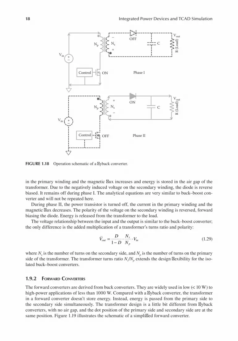
18 Integrated Power Devices and TCAD Simulation
in the primary winding and the magnetic flux increases and energy is stored in the air gap of the transformer. Due to the negatively induced voltage on the secondary winding, the diode is reverse biased. It remains off during phase I. The analytical equations are very similar to buck–boost con-verter and will not be repeated here.
During phase II, the power transistor is turned off, the current in the primary winding and the magnetic flux decreases. The polarity of the voltage on the secondary winding is reversed, forward biasing the diode. Energy is released from the transformer to the load.
The voltage relationship between the input and the output is similar to the buck–boost converter; the only difference is the added multiplication of a transformer’s turns ratio and polarity:
=
−⋅ ⋅V
D
D
N
NVout
s
pin
1 (1.29)
where Ns is the number of turns on the secondary side, and Np is the number of turns on the primary side of the transformer. The transformer turns ratio Ns/Np extends the design flexibility for the iso-lated buck–boost converters.
1.9.2 ForwArd converters
The forward converters are derived from buck converters. They are widely used in low (< 10 W) to high-power applications of less than 1000 W. Compared with a flyback converter, the transformer in a forward converter doesn’t store energy. Instead, energy is passed from the primary side to the secondary side simultaneously. The transformer design is a little bit different from flyback converters, with no air gap, and the dot position of the primary side and secondary side are at the same position. Figure 1.19 illustrates the schematic of a simplified forward converter.
Vout
Phase I
Phase IIOFF
ON
ON
OFF
Np
Np
Ns
–
+
Ns
+
–C
C
Vout
R (L
oad)
R (L
oad)
Control
Vin–+
Control
Vin –+
FIGURE 1.18 Operation schematic of a flyback converter.

19Power Electronics, the Enabling Green Technology
Since the mode of operation is very similar to the buck converter, detailed analysis is omitted. The input–output voltage relationship is the same as the buck converter except that it is multiplied by the transformer’s turns ratio:
= ⋅ ⋅V D
N
NVout
s
pin
(1.30)
In practice, a third winding is always necessary with a third diode, as shown in Figure 1.20, because during the transistor’s off state the energy stored in the transformer needs to be dissipated. With the third winding, a current will be forced through the diode, D3, until the stored energy is fully dissipated before the transistor is turned on again for the next switching cycle.
1.9.3 Full-Bridge converters
Full-bridge converters are derived from buck converters, similar to the forward converters. They are mainly used in high-power applications (750 W and up) [17]. In our previously discussed convert-ers, only one power transistor is used; full-bridge converters use four power transistors on the pri-mary side. At lower power levels, the forward converter is preferred over the full-bridge converter because of its lower parts count. The transformer is designed in such a way that the secondary side has a winding with a centered tap. The schematic of a simplified full-bridge converter is shown in Figure 1.21.
D1
D2Np
S
Ns
LC
R (L
oad)
Vin
–+
FIGURE 1.19 Schematic of a simplified forward converter.
D1
D2
D3
Np
S
Ns
L
C
R (L
oad)
Vin
–+
FIGURE 1.20 A more practical forward converter schematic.

20 Integrated Power Devices and TCAD Simulation
Operating a full-bridge converter is a little bit more complicated than forward or flyback convert-ers. The diagonal switches S1, S4 and S2, S3 are turned on in combination during each half-cycle of the converter, and the transformer primary side winding is provided with the full input voltage. The polarity of the transformer reverses in each half cycle [18]. Figure 1.22 illustrates the operation principle of the full-bridge converter.
The input–output voltage relationship can be derived as [17]
= ⋅ ⋅V D
N
NVout
s
pin
(1.31)
S2S1
S4S3
D2
D1 Vout
NpNs
Ns
L
C
R (L
oad)Vin
–+
FIGURE 1.21 Simplified schematic of a full-bridge converter topology.
S2S1
S4S3
D2
D1Vout
Np
++
–
–
Ns
ON
OFFOFF
OFF
ONPhase I
Phase II
ON
Ns
L
C
R (L
oad)Vin
–+
S2S1
S4S3
D2
D1 Vout
Np–
+
–+
Ns
OFF
ONON
OFF ON
OFF
Ns
L
C
R (L
oad)Vin
–+
FIGURE 1.22 Operation schematic of a full-bridge converter.
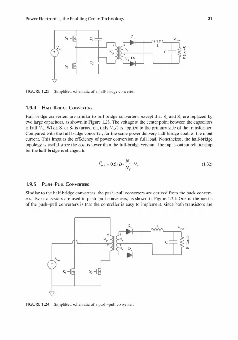
21Power Electronics, the Enabling Green Technology
1.9.4 HAlF-Bridge converters
Half-bridge converters are similar to full-bridge converters, except that S2 and S4 are replaced by two large capacitors, as shown in Figure 1.23. The voltage at the center point between the capacitors is half Vin. When S1 or S2 is turned on, only Vin/2 is applied to the primary side of the transformer. Compared with the full-bridge converter, for the same power delivery half-bridge doubles the input current. This impairs the efficiency of power conversion at full load. Nonetheless, the half-bridge topology is useful since the cost is lower than the full-bridge version. The input–output relationship for the half-bridge is changed to
= ⋅ ⋅ ⋅V D
N
NVout
s
pin0.5
(1.32)
1.9.5 pusH–pull converters
Similar to the half-bridge converters, the push–pull converters are derived from the buck convert-ers. Two transistors are used in push–pull converters, as shown in Figure 1.24. One of the merits of the push–pull converters is that the controller is easy to implement, since both transistors are
S1
S2
C1
C2
D2
D1 Vout
NpNs
Ns
LC
R (L
oad)Vin
–+
FIGURE 1.23 Simplified schematic of a half-bridge converter.
S1 S2
D2
D1 Vout
Np Ns
Ns
L
C
R (L
oad)
Vin
–+
FIGURE 1.24 Simplified schematic of a push–pull converter.

22 Integrated Power Devices and TCAD Simulation
operated at the low side (i.e., power MOSFETs source/body terminals are grounded). The input–output relationship can be expressed as
= ⋅ ⋅ ⋅V D
N
NVout
s
pin2
(1.33)
1.9.6 AdditionAl topics in isolAted dc/dc converters
1.9.6.1 Synchronous Rectification of Isolated DC/DC ConvertersAlthough we used diodes D1 and D2 in previous isolated topologies on the secondary side, in real application synchronous rectification with active MOSFET transistors are used to increase the power conversion efficiency, as seen in Figure 1.25.
1.9.6.2 Power MOSFET Parallel Body Diode ConductionPower MOSFET has an inherent parasitic body diode (which is not the case with IGBT or LIGBT), formed by the drain and body regions. As seen in Figure 1.26, this intrinsic body diode profoundly affects the performance of DC/DC converters. As an example, during the dead time of a full-bridge converter, the only current flow path is through the diodes, as seen in Figure 1.27. When S2 and S3 are turned off and before S1 and S4 are turned on, the current cannot change immediately due to the leakage inductance of the transformer. The current flow is then diverted through the body diodes of S1 and S4 until S1 and S4 power transistors are turned on (with very low drain to source voltage) at the onset of the next switching cycle.
S1 S2
S3 S4
S5
S6
Vout
NpNs
Ns
L
C
R (L
oad)Vin
–+
FIGURE 1.25 Schematic of a full-bridge converter with synchronous rectification.
GateP
N
FIGURE 1.26 Intrinsic body diode in a power MOSFET.

23Power Electronics, the Enabling Green Technology
1.9.6.3 Transformer UtilizationWhile a detailed analysis of transformers is out of the scope of this book, a brief mentioning of transformer utilization in different isolated DC/DC converter topologies is still necessary. As we have seen, the flyback and forward converters use only one coil in the secondary side, which means that flux swings in only one quadrant of the B–H curve. This implementation is called single-ended. For the full-bridge, half-bridge, and push–pull converters, two quadrants of the B–H curve are used. These converters are then named as double-ended. For a given set of requirements, a double-ended topology requires a smaller core than a single-ended topology and does not require an additional reset winding [19]. Therefore, higher power density can be achieved with double-ended topologies.
1.9.6.4 Voltage Stress on the Active Power TransistorDuring the operation of power converters, the power transistors could suffer from voltage stress. The stress level is different from topology to topology and is an important criterion of selecting the right power transistors. Table 1.5 illustrates the comparison between topologies. As we can see, full-bridge and half-bridge converters suffer the lowest voltage stress.
S1 S2
S3 S4 ON
ON
OFFOFF
OFFOFF
D1
D2
Vout
Np
Ns
Ns
L
C
R (L
oad)Vin
–+
FIGURE 1.27 The current flows through the MOSFET’s body diodes during dead time.
TABLE 1.5Comparison of Isolated DC/DC Converter Topologies
TopologiesPower
Range (W)Transformer Utilization
Active Switch
Number Output Voltage Voltage Stress Cost
Flyback < 100 Single-ended 1
=−
⋅ ⋅V DD
NN
V1out
s
pin
> + ⋅V N
NVin
s
pout Lowest
Forward 50~200 Single-ended 1
= ⋅ ⋅V D NN
Vouts
pin > V2 in >Flyback
Push–pull 100~500 Double-ended 2
= ⋅ ⋅ ⋅V D NN
V2outs
pin > V2 in >Flyback
Half-bridge 100~500 Double-ended 2 = ⋅ ⋅ ⋅V D NN
V0.5outs
pin >= V0.5 in >Push–Pull
Full-bridge > 500 Double-ended 4
= ⋅ ⋅V D N
NVout
s
pin > = Vin >Half-bridge

24 Integrated Power Devices and TCAD Simulation
1.9.7 compArison oF isolAted dc/dc converter topologies
A comparison of the isolated DC/DC converter topologies is given in Table 1.5 [19]. A flyback converter uses only one power switch and no inductor at the secondary side, which makes it the easiest topology to implement and with the lowest cost. However, the problem with flyback is the poor transformer utilization (single-ended) and high voltage stress on the active power transistor. The forward converter is somewhat similar to the flyback converter and is single-ended with lower power density. Push–pull, half-bridge, and full-bridge are all double-ended converters. The push–pull converter suffers from high voltage stress. The half-bridge converter has a much lower peak voltage at the primary side. The full-bridge converter has the benefits of double-ended design, with relatively low voltage stress on the transistors. It also has a reduced input current when compared with the half-bridge converter. The issue with the full-bridge converter is the complicated control for four transistors. It easily becomes the most costly converter of the group.
1.10 SPICE CIRCUIT SIMULATION
PSPICE [20] can be used to simulate power converters. As an example, a boost converter is simulated using PSPICE with schematic and simulation windows as shown in Figures 1.28 and 1.29. Here, the MOSFET is controlled by a pulse generator, with a pulse width = 5 µs, period = 10 µs, and a fixed duty cycle D = 0.5. From basic calculation, we know the output voltage is related to input voltage with
=
−V
DVout in
11
(1.34)
12 VV1
IRF150
100 uHD1N4002
L1V
V
V
200R1C11u
V3
M1
+–
0
–
+
D4
FIGURE 1.28 PSPICE schematic of a boost DC/DC converter.
FIGURE 1.29 Simulation result of a boost DC/DC converter.

25Power Electronics, the Enabling Green Technology
With input voltage of 12 V, the output voltage is found to be 24 V at steady state. The fluctuation of output voltage at the beginning reflects the time needed to establish steady state.
The main focus on this book is on the design and operation of the power devices using TCAD simulation tools. SPICE circuit simulations represent the next design step in the development pro-cess. This topic is widely covered by numerous books and will not be repeated here.
1.11 POWER MANAGEMENT SYSTEMS FOR BATTERY-POWERED DEVICES
Power electronics typically applies to board-level switched-mode power converters where discrete power elements such as power transistors, power diodes, capacitors, inductors, transformers, resis-tors, and controller ICs are packed and connected on a PCB board. This implementation is simple and flexible, capable of converting large amounts of power. With higher switching frequencies, the volume of the magnetic components can be made smaller, allowing the power density to increase. However, for very low-power applications, such as the battery-operated mobile devices, the bulky form factor is not convenient for users. Except for battery chargers (AC adapters), the conversion of battery power in a mobile device to supply the various components such as a CPU and LCD screen typically relies on integrated solutions. We refer to these integrated solutions as power management systems for battery-powered devices.
Power management systems can be regarded as a group of power converter circuits. They are becoming more diversified to keep up with the demands of modern mobile electronics systems. As an example, the power management system in a modern 3G smartphone is illustrated in Figure 1.30. It consists of many functioning units, each of which requires a different dedicated power supply [21]. Figure 1.31 is a more detailed illustration of the power management architecture of a battery-operated system with various functional blocks [22] [23]. Step-down DC/DC converters (e.g., buck converters) are used for DSP and microprocessors that require a lower voltage input, while induc-torless DC/DC charge pumps are used for noise-sensitive RF circuitry since switched mode power converters typically bring some current and voltage ripples.
AudioBaseband
(DSP, ARM,Memory)
RF Up andDown
PLL and VCO
Bluetooth
W-LED BacklightVibrator Motor
Digital CameraMotor
Digital CameraImage Sensor
LCD Display
3G Cell Phone PowerManagement System
5 V3.3 V
15 V
15 V
–7.5 V
3.3~5 V
3.3~5 V ConstantCurrent
3.3 V
2.8 V
2.8 V1.2~2.5 V
2.5~3.3 V
1.1~1.5 V2.5 V
FIGURE 1.30 A typical example of 3G smartphone power management system.

26 Integrated Power Devices and TCAD Simulation
1.12 SUMMARY
This chapter is intended to give a broader view to power device engineers since the main applica-tions of power devices are power electronics and power management systems. In the next chapter, we will continue with an introduction to power management ICs where integrated power devices are typically used. Later chapters focus on the description of various types of power semiconduc-tor devices such as diodes, power MOSFETs, and LIGBTs. In particular, we will provide detailed explanations on how TCAD tools can be used to analyze and design these devices.
Audio Supply
Step-up DC/DCConverters
InductorlessDC/DC Regulators
(Charge Pumps)
BatteryManagement
RechargeableBattery
ChargerFront-EndProtection Battery Charge
Management
Li-ionProtection andAuthentication
for Batteries
Battery FuelGauges
I2C ResetDSPµP
Step-DownDC/DC Converters
Linear Regulators
LCD BiasSolutions
White LED Drivers
Photo FlashCapacitor Chargers
Application-SpecicMulti-Output
Solutions
SystemVoltages
Photo Flash
LED Lights
LCD ColorDisplayLCD
MemoryMemory
Supervisory Circuits(Voltage Supervisors)
DC Inputs
USB
– +
Noise-sensitive RFCircuitry
FIGURE 1.31 A more detailed power management architecture for a battery operated system (after Texas Instruments’ Power Management Guide 3Q 2008).

27
2 Power Converters and Power Management ICs
Chapter 1 briefly reviewed the topologies of power converters. This chapter focuses on integrated power converters and power management ICs. Smart power ICs are a special class of integrated circuits that combine the decision-making circuits (the smart) and the power switches (the muscle) to deliver power to a load in an intelligent and efficient way. This chapter introduces the concept of power management and the corresponding smart power IC implementation via several examples. The fabrication technologies and semiconductor devices that are used to implement smart power ICs will be discussed in Chapters 7 and 8.
2.1 DYNAMIC VOLTAGE SCALING FOR VLSI POWER MANAGEMENT
Power management is the technique used to deliver power or to manipulate the power supplies effi-ciently without interfering with the normal operation of the load. An example of power management architecture for a battery-operated system is already introduced in Figure 1.31. This power manage-ment architecture can be further subdivided into different DC/DC converters, voltage regulators, and output drivers to accommodate the specific requirements of each load. A popular example of power management techniques is the dynamic voltage scaling (DVS) for optimizing the power con-sumption of the digital signal processor/microprocessor (DSP/µP) chip. In DVS, the supply voltage to a DSP/µP chip is reduced to a level that is just sufficient to achieve a target operating frequency. This technique relies on the fact that real-time computing tasks (such as frame decoding) often result in predictable workloads, and therefore the power management algorithm can dynamically select a target frequency to allow “just-in-time” completion of the tasks. A competing strategy for power reduction, known as dynamic threshold scaling (DVTS), uses external substrate biasing to dynamically control VTH and reduce both dynamic and leakage power consumption [24] [25]. DVTS is more advantageous in nanotechnologies below 0.13 μm, where subthreshold leakage power domi-nates. The simulated power savings using DVS and DVTS for a ring oscillator in a 0.18 μm CMOS process are as shown in Figure 2.1a.
From basic CMOS logic gate analysis, it is well-known that the dynamic power dissipation Pdynamic is proportional to
∝⋅ ⋅ ⋅P C V fdynamic DD2 (2.1)
where C is the load capacitance (usually the input gate capacitance of the next stage), VDD is the supply voltage, and f is the clock frequency. The dynamic power dissipation in a generic digital circuit can be reduced by simply reducing f. This results in a linear reduction of the power consump-tion as shown by the “no scaling” line in Figure 2.1b. It is also interesting to note that in modern deep submicron and nanoscale CMOS technologies this linear curve does not intersect the origin as the frequency is scaled to DC. This indicates that a significant amount of static power is being dissipated due to leakage current. In DVS, both VDD, and f are scaled to achieve a quadratic power saving during low demand cycles. DVTS provides additional power saving. However, the range of operation is limited due to the need to generate the extra substrate bias voltage.
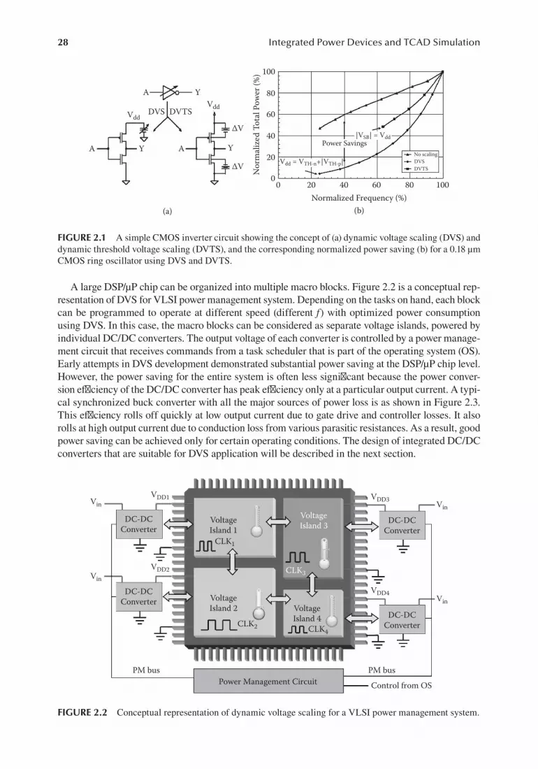
28 Integrated Power Devices and TCAD Simulation
A large DSP/µP chip can be organized into multiple macro blocks. Figure 2.2 is a conceptual rep-resentation of DVS for VLSI power management system. Depending on the tasks on hand, each block can be programmed to operate at different speed (different f) with optimized power consumption using DVS. In this case, the macro blocks can be considered as separate voltage islands, powered by individual DC/DC converters. The output voltage of each converter is controlled by a power manage-ment circuit that receives commands from a task scheduler that is part of the operating system (OS). Early attempts in DVS development demonstrated substantial power saving at the DSP/µP chip level. However, the power saving for the entire system is often less significant because the power conver-sion efficiency of the DC/DC converter has peak efficiency only at a particular output current. A typi-cal synchronized buck converter with all the major sources of power loss is as shown in Figure 2.3. This efficiency rolls off quickly at low output current due to gate drive and controller losses. It also rolls at high output current due to conduction loss from various parasitic resistances. As a result, good power saving can be achieved only for certain operating conditions. The design of integrated DC/DC converters that are suitable for DVS application will be described in the next section.
VDD1
VDD2
Vin
Vin
VDD3
VDD4
Vin
Vin
DC-DCConverter
VoltageIsland 1
VoltageIsland 2
VoltageIsland 3
VoltageIsland 4
CLK1
CLK2
CLK3
CLK4
DC-DCConverter
DC-DCConverter
DC-DCConverter
PM busPM busPower Management Circuit Control from OS
FIGURE 2.2 Conceptual representation of dynamic voltage scaling for a VLSI power management system.
A
A
(a)
A
DVS
Y
Y
DVTSVdd
Vdd
∆V
100
80
60
40
20
00 20 40
|VSB| = Vdd
Vdd = VTH-n+|VTH-p|
Power SavingsNo scalingDVSDVTS
Normalized Frequency (%)
Nor
mal
ized
Tot
al P
ower
(%)
(b)
60 80 100
∆V
Y
FIGURE 2.1 A simple CMOS inverter circuit showing the concept of (a) dynamic voltage scaling (DVS) and dynamic threshold voltage scaling (DVTS), and the corresponding normalized power saving (b) for a 0.18 μm CMOS ring oscillator using DVS and DVTS.

29Power Converters and Power Management ICs
2.2 INTEGRATED DC/DC CONVERTERS
To enjoy the full benefits of DVS power management, high-performance DC/DC converters with a flat power efficiency curve is required. At the same time, the form factor of the converters must be reduced to provide a high power density (power-to-volume ratio). Switched mode power sup-plies (SMPS) such as the DC/DC converters rely on an inductor as the energy storage element and a capacitor as a smoothing filter. The size of the inductor and capacitor is inversely proportional to the switching frequency of the DC/DC converter. As can be seen from Figure 2.4, the increase in switching frequency leads to a progressively smaller form factor. As the switching frequency approaches the multiple MHz range, it is also possible to combine the inductor and capacitor into the smart power IC package. Even though it is possible to implement integrated DC/DC converters with switching frequencies in the 10s to 100s MHz range, the high-frequency magnetic core losses pre-vented the use of ferrite core inductors. However, air core inductors have a large form factor, reduc-ing the attractiveness of high switching frequency. In addition, switching loss also increases with frequency, causing a roll-off in the power conversion efficiency as shown in Figure 2.5. Currently, converters with switching frequencies in the multiple MHz range appear to be a good compromise between form factor and power efficiency.
ESRLoss
ESRLoss
GateDrive
FETsSwitching &Conduction
RL Loss
Vo
Cout
CinVg
Controller
ControllerBiasing &Switching
Body DiodeConduction
(a) (b)
+–
MP
MN iLOAD Effici
ency
(%)
100
75
50
25
00 100
Iout (mA)
Gate drive &Controller
ConductionLoss
200 300
L
FIGURE 2.3 (a) A typical buck converter topology with all the major sources of loss identified. (b) The power conversion efficiency for a buck converter as a function of output current level.
500 kHz
1 MHz
2 MHz
10 MHz
FIGURE 2.4 Benefits of miniaturization via high level integration using smart power IC fabrication technol-ogy, specialized packaging, and increased switching frequency.

30 Integrated Power Devices and TCAD Simulation
The characteristics of the power conversion efficiency in DC/DC converters is dependent to a large extent on the choice of the power transistors for the output stage. The typical output stage is a half-bridge configuration as shown in Figure 2.6. The totem pole design, which uses two N-channel power transistors for the high side and low side drivers or the push–pull design, which uses a P-channel power transistor for the high side driver and an N-channel power transistor for the low side driver, are two approaches to implement the half-bridge output stage. For integrated DC/DC converters, the choice on which configuration to use depends on the available power devices in the particular smart power IC fabrication technology. This topic will be covered in Chapters 4 and 8. Basically, the low-side (LS) power transistor is always an N-channel device due to the lower specific on-resistance (in mΩ⋅cm2, resistance normalize to a unit area) and simple gate drive signal requirement. The high-side (HS) power transistor can be either an N- or P-channel device. Generally, the N-channel device is preferred due to its inherent low specific on-resistance. This is because the electron mobility is approximately three times higher than the hole mobility. As a result, for the same on-resistance, the N-channel device can be three times smaller than a P-channel device with similar rating. The smaller device area will translate directly to a lower cost. However, the trade-off in choosing an N-channel HS power transistor is the more complex gate driver requirement. A gate signal higher than the
100
80
60
400.5 1.5
ConductionLoss
Switching LossL = 150 nHL = 200 nHL = 250 nHL = 300 nHL = 350 nH
2.5Switching Frequency (MHz)
Eci
ency
(%)
3.5 4.5 5.5
FIGURE 2.5 Power conversion efficiency for a typical DC/DC converter as a function of switching fre-quency and inductor size.
VDD
VDD
VDD
VBootstrap
GND
GNDn-MOS
n-MOS
(a)
L VOUT
S2
S1
C
VDD
VDD
VDD
GND
GNDp-MOS
n-MOS
(b)
L VOUT
S2
S1
C
FIGURE 2.6 Output stage designs for a buck converter: (a) a totem pole output stage using N-channel power transistors for both the HS and LS drivers; (b) a push–pull output stage using complementary N- and P-channel power transistors.

31Power Converters and Power Management ICs
supply voltage is required to fully turn on the N-channel transistor. This usually involves a bootstrap circuit, consisting of an external or integrated diode and an external capacitor. However, the most critical decision is based on whether the smart power IC fabrication technology offers a floating source N-channel device (the source terminal has to swing between GND and VDD).
The on-resistance, gate capacitance, and switching speed of the transistors are the critical param-eters that determine the peak power conversion efficiency. In general, the size of the transistors is proportional to the nominal output current.
2.2.1 segmented output stAge
In a practical situation, the load current can change drastically as the system operates between full power and standby mode. In a DVS system, the DC/DC converter is also required to provide effi-cient power delivery at different output voltages and currents. The concept of using a combination of small and large transistors for the output stage was first introduced by Williams et al. [26] as shown in Figure 2.7. For a light load, it is more advantageous to use a small size transistor to reduce the gate drive loss. Since the output current is small, the high on-resistance from the small transistor will not lead to significant conduction loss. Therefore, good power conversion efficiency can be achieved. For a heavy load, there is no choice but to use the largest transistor available to reduce the conduc-tion loss. Depending on the switching frequency, the gate drive and switching loss incurred by the large size transistor will be less dominant when compared with the conduction loss.
While this concept is straightforward, the implementation is rather difficult because it not easy to monitor the output current (especially for low output voltage, such as 1 V for most µP chips). In addition, switching the size of the power transistors on the fly may also lead to instability of the control loop. As a result, this remained as an interesting concept until the advent of the digital con-troller for DC/DC converters. With the development of the digital controller, various nonintrusive, sensorless sensing techniques have also been developed [27]. For example, the output current of a buck converter can be easily deduced if the input voltage, output voltage, PWM duty ratio, and the on-resistance of the power transistors are known [28]. In addition, the digital controller can also reconfigure itself on the fly to ensure stable operation on an as needed basis. These developments lead to the practical demonstration of a simple DC/DC converter with automatic selection of out-put transistor sizes according to the output current level. The architecture of a digitally controlled DC/DC converter with a segmented output stage is as shown in Figure 2.8. The block diagram is similar to a conventional digitally controlled DC/DC converter with an ADC to monitor the output voltage (Vout) and compare it with a reference voltage (Vref). The error voltage e[n] is fed to a digital
Heavy Load
Gate DriverGate Driver
VinVin
“O ”
“O ”
K
K
1
1
K
K
1
1
+–+–vout(t)vout(t)
Light Load
(b)(a)
FIGURE 2.7 The “Dual-Gate W-Switched Power MOS” originally proposed by R. Williams et al. in ISPSD’97 [26]. For a heavy load, both large (K) and small (1) power transistors are activated (a); for a light load, only the small power transistor is used (b).

32 Integrated Power Devices and TCAD Simulation
PID controller, which in turn generates the duty command d[n]. The PWM waveform is then gen-erated via the DPWM module. After the appropriate dead times are incorporated, the gate drive signals are sent to the power transistors via the gate driver. If PFM (pulse frequency modulation) operation is desired, a mode selector can be used to choose PWM or PFM. The major difference is the segmented output stage. In this design, the sizes of the power transistors (both high side and low side) are actually the same as in a conventional design with the same output current rating. The only difference is in terms of organization. In this case, the HS and LS power transistors are organized into seven equal segments and basically occupy the same area as one big transistor. The segments are connected in binary weighted 1, 2, and 4 segments such that a three-bit control signal can activate seven different transistor sizes (from size 1 to 7). The only additional control circuits introduced are the current estimator and segment controller blocks. The output current is estimated based on
= −
IDV V
rout
out out (2.2)
where r is the converter’s series resistance, r = DRon,P + (1 − D)Ron,N + RL ≈ Ron + RL, with RL being the inductor’s series resistance, and D is the steady-state duty ratio. In a digital controlled DC/DC converter, all these parameters are known. As a result, the current estimator can calculate the output current level and decide on the most appropriate size of the HS and LS power transistors.
The die micrograph of the integrated DC/DC converter with segmented output stage is as shown in Figure 2.9. This test chip includes extra circuitries and look-up tables. The actual die size for a 5 V to 1 V, 1 A output converter can be 2 mm × 1.25 mm for this 0.18 µm CMOS implementation. The diagonal metal lines in the power transistors are the results of the use of a hybrid waffle layout. This technique allows an optimized trade-off between the metal interconnect resistance and the intrinic on-resistance of the power MOSFET [29]. In addition, an IC package showing a built-in energy storage induc-tor to save a circuit board footprint is also included in Figure 2.10. The measured power conversion
Gate Driver
L
C
ADC
Vref
Vin[n]
e[n]d[n]
[2]
[2]
Segmented Output Stage
MSB
[1][0]
[1][0]LSB
Vin(t)+
–
1
0
Vin[n]
Iout[n]en_N[2:0]
en_P[2:0]
N[2:0]
P[2:0]
d[n]
CurrentEstimator
DigitalPID
DPWM
PFM
SegmentController
Dead-TimeGenerator
Mode –+
R
vout(t)
FIGURE 2.8 Architecture of the segmented output stage and the digital controller. Seven identical segments are paired to achieve three binary-weighted segments.

33Power Converters and Power Management ICs
efficiency of the DC/DC converter running at 4 MHz with Vin = 2.7 V, Vout = 1.8 V for different output transistor sizes are as plotted in Figure 2.11. The benefit of having the ability to switch to different power transistor sizes according to output current level is immediately apparent. For example, it is more advantageous to use large power transistors (size 111 = 7) for high output current and a small size transistor (size 001 = 1) for low output current. At very low current level, the power conversion
VX
1.25 mm
VDD
_PW
R
VSS_
PWR
FIGURE 2.9 Die micrograph of an integrated DC/DC converter with segmented output stage. The test chip contains extra test circuits and look-up table. The actual die size for a 5 V to 1 V, 1 A output converter can be 2 mm × 1.25 mm for this 0.18 µm CMOS implementation.
M3–M6Source Wire
M2 Gate Wires
Poly Gate
DiusionWc
Wr
SDS
S
M3–M6 Drain WireM1–M6 contactM1–substrate contactPoly-M1–M2 contact
2.4 mm
2.95 mm
pMOS nMOS
nMOS DriverspMOS Drivers
1 Se
gmen
t
1 Se
gmen
t
1 mm
DS
DSD
FIGURE 2.10 Zoomed-in view of the segmented output stage. The diagonal metal lines are the result of the hybrid waffle layout for the optimized trade-off between metal interconnect resistance and the intrinsic resis-tance of the power MOSFETs. Also shown in this figure is the IC package with a built-in inductor.

34 Integrated Power Devices and TCAD Simulation
efficiency can be further improved by changing to a PFM operation. This type of power conversion efficiency optimzation is essential for a true DVS power management system for VLSI applications.
2.2.2 trAnsient suppression witH An AuxiliAry stAge
In addition to providing efficient power conversion, point-of-load (POL) DC/DC converters driving mod-ern microprocessors need to provide low output voltage, high output current, and good dynamic perfor-mance during load transients. Digitally controlled DC/DC converters have shown more flexibility over their analog counterparts with the introduction of intelligent control techniques such as the auto-tuning system that can tolerate passive component variations [30], the segmented output stage that can dynami-cally adjust the size of the output transistors according to load conditions to maintain high-power conver-sion efficiency [31], and the one-step dead-time correction that can optimize the turn-on and turnoff dead time for power transistors on the fly [32]. They also have the ability to switch seamlessly between linear and nonlinear operation modes and achieve near-optimal load transient performance [33].
In this design example, a fully integrated DC/DC converter utilizes digitally controlled dual output stages to achieve fast load transient recovery. As shown in Figure 2.12, it consists of a main converter output stage connected in parallel with an auxiliary output stage. The main output stage is responsible for steady-state operation and is designed to achieve high conversion efficiency using large inductor and power transistors with low on-resistance. The auxiliary stage is responsible for transient suppression and is active only when a load transient occurs.
The need for the auxiliary output stage can be illustrated by the theoretical current waveforms dur-ing a heavy-to-light load transient as shown in Figure 2.13. In general, the large inductor in the main output stage is too slow to react to a sudden change in output current. As a result, the output voltage will exhibit an undesired overshoot or droop until the PID controller recovers. This change in output voltage may cause the digital circuits in the POL to change states inadvertently. Therefore, it is impor-tant to make use of a smaller size inductor in the auxiliary stage to suppress this disturbance within a short time. The proposed control method involves three control parameters: the main stage recovery time (TR), turn-on time (ton), and turnoff time (toff), which represent the on-time for transistors LSmain, LSaux, and HSaux, respectively. In the case of heavy-to-light load transients, during TR, the inductor current in the main output stage (ILM) ramps down with a slope of k1 until it reaches the targeted load current. In the meantime, the auxiliary stage is activated to help sink current with a high slew rate: dur-ing ton the auxiliary stage inductor draws current (ILA) from the output filter capacitor and then ramps
95Vin = 2.7 V, Vout = 1.8 V, fs = 4 MHz
90
85
80
75
70
65
601 10
Output Current (mA)
111100011101PFM 111PFM 001
100 1000
FIGURE 2.11 Measured power conversion efficiency for the integrated DC/DC converter with segmented output stage. The transistor size ranges between 001 to 111.

35Power Converters and Power Management ICs
To HSaux
HSaux
LSaux
To LSauxTo HSmain
HSmain
LSmain
Digital Controller
Main Converter
Cout
Vout
Vout
Iout
+
–
Vin
+
–
LM
LA
VXAAux. Stage
VXM
To LSmain
FIGURE 2.12 A digitally controlled POL DC/DC converter with an auxiliary output stage for fast load transient recovery.
i(t)Iout
ILM
ILA
TR
ton to
k1
k3
k2
∆Iout
∆Iout
0ti(t)
0t
i(t)0
t
FIGURE 2.13 Theoretical waveforms of load current (Iout), main stage inductor current (ILM), and auxiliary stage inductor current (ILA) under heavy-to-light load transient taking into account the auxiliary switches’ on-resistances.

36 Integrated Power Devices and TCAD Simulation
back to zero through toff. The switching commands for both the main and the auxiliary output stage are determined based on the capacitor charge balance principle [34], such that the amount of charge released through the auxiliary stage equals the excess charge injected by the main stage. By equating the areas of the two shaded regions in Figure 2.13, the three control parameters can be obtained from solving (2.3)–(2.5). This method aims at recovering the output voltage to its steady-state value with one set of switching actions. Full details on the operation and controller design can be found in [35]. The focus in this section is to describe the implementation of this type of converter.
=T
I
kR
out
1 (2.3)
∫ + =I t dt
I t
k
I
k
t
LALA on out
on
( )( )
20
2
3 12
(2.4)
=t
I t
koff
LA on| ( )|
3 (2.5)
If this dual output stage transient suppression converter were to be built using discrete com-ponents, the PCB footprint would be effectively doubled, making this design twice as costly as well. For example, even though one can choose power transistors with different ratings, the size of the packages would essentially be the same. As a result, there will be no real area, size, and weight savings. However, in a monolithic implementation, the designer is free to choose different transistor sizes and the complete converter can be integrated onto one silicon die inside one pack-age. The die micrograph of the DC/DC converter with a main output stage and an auxliary output stage for transient suppression is as shown in Figure 2.14. This converter is implemented using TSMC’s 0.25 µm CMOS technology with 12 V option. The specifications and test conditions for this converter are summarized in Table 2.1. The main output stage transistors are designed to achieve a peak efficiency of around 90%. The auxiliary stage transistors are sized following the
DigitalController
GateDrivers
LSAux
GNDGND
VinVin
LSMainLSMain
HSMainHSMain
HSAuxHSAux
Auxiliary StageSwitching Nodes
Main StageSwitching Nodes
FIGURE 2.14 Micrograph of the integrated DC/DC converter (Die size is 2.35 mm × 2.35 mm).

37Power Converters and Power Management ICs
criteria discussed in [36]. From the die micrograph, it can be observed that the auxiliary output stage imposes less than 20% area overhead. Transient performance of the prototype converter was measured under the test condition specified in Table 2.1. Transient output voltage waveforms for a conventional single-stage PID controller and the proposed dual-output-stage controller are compared in Figures 2.15a and b. For a 2.25 A to 0.25 A load transient, a reduction in recovery
0.11Iout = 2.25 A Iout = 0.25 A
Iout = 2.25 A Iout = 0.25 A
Recovery Time
Recovery Time
V out
– V
ref [
V]
V out
– V
ref [
V]
Time [s](a)
1E–40E+0–1E–4 2E–4 3E–4 4E–4
Time [s](b)
1E–40E+0–1E–4 2E–4 3E–4 4E–4
0.090.070.050.030.01
–0.01–0.03–0.05
0.06
0.04
0.02
0.00
–0.02
–0.04
FIGURE 2.15 Dynamic response under a 2.25 A to 0.25 A load transient using (a) conventional single-stage PID controller and (b) dual output stages.
TABLE 2.1Summary of Specifications and Test Conditions
Parameters Values
Die area 2.35 mm × 2.35 mm
PMOS_Ron(HS) 200 mΩ
NMOS_Ron(LS) 20 mΩ
PMOS_Imax(DC) 2.34 A
NMOS_Imin(DC) 3.24 A
Vin 6 V
Vout 1 V
LM (main stage) 2.2 µH
LA (aux stage) 820 nH
Cout 200 µF
Switching Frequency 390 kHz
ΔIout Switching from 2.25 A to 0.25 A

38 Integrated Power Devices and TCAD Simulation
time from 280 µs to 50 µs and in overshoot from 105 mV to 51 mV is observed. Since the auxiliary stage is disabled in steady state, the two control methods have a similar efficiency profile.
2.3 SUMMARY
In this chapter, the DVS power management technique for just-in-time processing has been intro-duced. Examples of two power management ICs have also been given. The segmented output stage can be used to effectively extend the power conversion efficiency over a wide range of output current levels. This is highly suitable for driving DVS systems. The second example involves a transient suppression technique using a dual output stage with a large inductor for high efficiency and a small inductor for fast transient. In both cases, clever arrangement of the power transistors and the use of control methods can greatly improve the functionality and performance of PMICs.
The next chapter discusses the semiconductor industry and the status of smart power IC technology.

39
3 Semiconductor Industry and More than Moore
As mentioned in the Preface, this book adopts a top-down approach. In Chapter 1, we discussed the power electronics system, which is the system-level application of power devices (mostly discrete). Power management ICs are presented in Chapter 2. Power management ICs are IC-level application of power devices (mostly integrated). Now we step further down the ladder to explore the foundation of the power management IC: the semiconductor industry.
3.1 SEMICONDUCTOR INDUSTRY
On July 1, 1948, the New York Times made an announcement about a new invention, “a device called a transistor, which has several applications in radio where a vacuum tube ordinarily is employed” [37]; the inventors did not yet know how much their invention would change the world. The semiconductor industry is now one of the most dynamic industries in the world and starting with the very first transis-tor at Bell Labs, it has now grown into a $US 280 billion industry. The total impact of the semiconduc-tor industry can be even greater: when electronics systems and services are included, it could be over $US 5 trillion, representing close to 10% of world gross domestic product (GDP) [38]. Figure 3.1 gives some key applications of semiconductor technology [39].
3.2 HISTORY OF THE SEMICONDUCTOR INDUSTRY
3.2.1 A BrieF timeline
A brief historical timeline of the semiconductor industry is listed in Table 3.1 [40]:
3.2.2 tHe trAitorous eigHt
One of the most notable people in the history of semiconductors is Nobel Prize winner William Shockley, the co-inventor of the first transistor. After this great invention, Shockley left Bell Labs to form a company called Shockley Semiconductor in Palo Alto, California, and hired some of the brightest scientists and engineers available. However, due to some managerial conflicts, a group of these (the famous “Traitorous Eight” [41]) left Shockley Semiconductor. Those eight men later made their own tremendous contributions to the semiconductor industry and are widely credited with the creation of the present-day “Silicon Valley.” Short biographies of these eight men are listed in Table 3.2.
3.2.3 HistoricAl roAd mAp oF tHe semiconductor industry
During the last decades, semiconductor chip performance advances have been mostly fueled by shrinking feature sizes and the use of larger wafers. Feature size is generally defined as the smallest gate length achievable by a certain lithography process. Supply voltage and junction depth need to shrink at the same time with the gate length to avoid the so-called short channel effect.
Table 3.3 illustrates the feature sizes and gate oxide thickness shrinking with time [42]. Please note that beyond 45 nm, materials with high dielectric constants (high-K) are used to reduce the

40 Integrated Power Devices and TCAD Simulation
leakage current that comes from ever thinner gate oxide. With high-K materials, thicker physical thickness materials with equivalent oxide thickness (EOT) of 1.2 nm can be used to reduce gate leakage current while achieving the same performance at 32 nm node. At the time of writing, the most advanced feature size that is commercially available is 22 nm, first introduced by Intel with FinFET (Tri-gate) technology on its latest Ivy-bridge processors [43], which packed 1.5 billion tran-sistors in its third generation “Core” processors [44].
The use of larger wafers brings no direct performance gain but lowers the average cost per chip for manufacturers since more chips can be packed onto the same wafer even if the feature size stays the same. From the 4 inch (100 mm) wafers used in 1975 to the 12 inches in use today, the wafers have gone through some major changes. If current trends continue, 18 inches (450 mm) will become the standard in a few years’ time. Figure 3.2 illustrates the evolution of wafer sizes.
Communications
Transportation Computing
ConsumerIndustrial
FIGURE 3.1 The semiconductor technology applications.
TABLE 3.1Historical Timeline of the Semiconductor Industry
Time Historical Event
1948 First transistor was invented at AT&T Bell Labs
1952 First Single Crystal Germanium introduced
1954 First Single Crystal Silicon introduced
1958 First Integrated Circuit invented by Jack Kilby of Texas Instruments
1961 First Integrated Circuit product by Robert Noyce of Fairchild
1971 Microprocessor was invented by Intel
1975 First commercial microprocessor unit (8086 and 6800)
1977 Apple and Radio Shack computers
1981 IBM personal computer introduced

41Semiconductor Industry and More than Moore
TABLE 3.2Brief Biographies of the Famous “Traitorous Eight” [41]
Name Brief Bios
Julius Blank Cofounder of Fairchild Semiconductor. He later founded Xicor, which was acquired by Intersil in 2004.
Victor Grinich Cofounder of Fairchild Semiconductor. He was later with University of California at Berkeley and Stanford University.
Jean Hoerni Cofounder of Fairchild Semiconductor. He was the inventor of the planar process, which allowed transistors to be created out of silicon rather than germanium. He later founded Intersil in 1967.
Eugene Kleiner Cofounder of Fairchild Semiconductor. He was the cofounder of Kleiner Perkins, the Silicon Valley venture capital firm that later became Kleiner Perkins Caufield & Byers.
Jay Last Cofounder of Fairchild Semiconductor. He later cofounded Amelco, which was acquired by Teledyne.
Gordon Moore Cofounder of Fairchild Semiconductor. He cofounded Intel Corporation in 1968. He is the author of the famous “Moore’s Law.”
Robert Noyce Cofounder of Fairchild Semiconductor. Nicknamed “the Mayor of Silicon Valley,” he was the cofounder of Intel with Gordon Moore, credited (along with Jack Kilby) with the invention of the integrated circuit.
Sheldon Roberts Cofounder of Fairchild Semiconductor. He later cofounded Amelco, which was acquired by Teledyne.
TABLE 3.3Historical Road Map of Feature Sizes and Gate Oxide Thickness
Year Feature Sizes Gate Oxide Thickness
1975 20 µm 250 nm
1980 10 µm 150 nm
1985 5 µm 70 nm
1990 1 µm 15 nm
1995 0.35 µm 8 nm
2000 0.18 µm 3 nm
2005 65 nm 1.4 nm
2010 32 nm 1.2 nm (EOT)
12 inch(2001)
8 inch(1991)
6 inch(1980)
4 inch(1975)
FIGURE 3.2 The evolution of wafer sizes.

42 Integrated Power Devices and TCAD Simulation
3.3 FOOD CHAIN PYRAMID OF THE SEMICONDUCTOR INDUSTRY
The semiconductor industry is structured similar to an inverted food chain pyramid [39] (Figure 3.3), where the upper levels of the pyramid require the output of the lower levels to function properly while the lower levels need guidance of the upper levels. The pyramid is inverted because in terms of industry size the upper levels employ more people than the lower levels.
3.3.1 level 1: wAFer And edA tools
The lowest level of the pyramid is the wafer suppliers and electronic design automation (EDA) tools suppliers. Please note that EDA in general supports all levels of the pyramid, from fundamental physics solvers (TCAD for device engineering) and IC design tools such as SPICE to system-level tools (thermal, mechanical, fluidic, and electromagnetic field).
The wafer business is the backbone of the electronics industry. Contrary to the dramatic reduc-tion of cost per transistor, the cost per wafer is steadily increasing due to the increased cost of tools and stricter requirements on material quality. However, since the wafers themselves are also grow-ing larger, the real cost per area is not that great. As an example, according to cost analysis from IC knowledge LLC [45], a 200 mm (8-inch) wafer is $1203.17 ($ 3.83 per cm2) compared with $1936.11 ($2.74 per cm2) for a 300 mm (12 inch) wafer. Since scaling of the feature size also produces more dies for the same area, lower costs per die can be achieved in spite of increasing wafer costs. For power IC applications, 6-inch and 8-inch bulk silicon wafers are typically used. Recently, Texas Instruments opened the industry’s first 12-inch wafer fab for analog and power management appli-cations in Texas [46].
To further reduce leakage current and increase digital gate density, sometimes Silicon on Insulator (SOI) wafers are used instead of bulk silicon. Companies such as Soitec can supply SOI wafers for power and analog applications with a rated breakdown voltage of up to 600 V [47]. SOI provides good isolation between power devices and analog/digital devices on the same die and may become the de facto standard with further feature size scaling. The biggest problems with SOI
Level 6. Product Marketing, Distributionand Sales
Level 5. System Architecture, SoftwareDevelopment
Level 4. Manufacturing, Packaging andTesting
Level 3. IC Design: Analog, Digital andMixed Signals
Level 2. Device Engineering: Discrete andIntegrated Devices
Level 1. Wafer and EDA tools
FIGURE 3.3 The inverted pyramid illustration of the semiconductor industry.
43Semiconductor Industry and More than Moore
wafers at the moment are higher costs (usually double the price of bulk wafers) and reduced thermal handling capability.
For power devices applications, compound materials such as SiC and GaN are also drawing attention due to their superior FOM (Figure of Merits). However, compound substrates such as SiC and GaN substrates are more expensive and only available in much smaller sizes compared with silicon. It has been reported that 6-inch substrates are becoming available for GaN [48] and 6-inch SiC substrates are under mass production [49].
The EDA industry is gaining a lot of momentum in recent years due to advances in digital circuit design and high-level abstraction for synthesis and routing. The EDA industry reached $1,619.9 mil-lion total revenue in the third quarter of 2012, up 4.9 percent from the third quarter of 2011, accord-ing to the EE Times [50]. As of 2013, the top three EDA companies in the world are Synopsys, Cadence, and Mentor Graphics [51].
For analog and power IC design, computer-aided design (CAD) tools are widely adopted. These tools use compact device models like BSIM3, BSIM4 [52], and PSP [53] implemented by hardware description language such as Verilog-A to create netlists for simulation. Compact models are mostly semi-empirical in that not all the model parameters are physical. This is especially true for power devices such as lateral double-diffused DMOS (LDMOS), which uses subcircuit models. LDMOS models are made available from multiple research institutes such as HiSIM (Hiroshima-University STARC IGFET Model) [54] and companies like NXP [55] and Freescale [56]. Generally speaking, compact models are technology dependent, which means the parameters need to be extracted for different process technologies; software tools such as IC-CAP from Agilent are usually used for parameter extraction from measurement [57], and the models are subsequently provided to design-ers through a Process Design Kit (PDK).
Technology computer-aided design (TCAD) is a special category within EDA. Rather than being used to design ICs, these tools operate at a lower level of abstraction and are used by semiconductor device engineers to design process flows and various kinds of semiconductor devices. More detailed treatment of TCAD tools will be given in Chapters 5 and 6.
3.3.2 level 2: device engineering
The second level is device engineering, which consists of both process integration and device design. Device engineers are “customers” of the wafer suppliers and EDA (TCAD) vendors. They will define and select the most appropriate starting wafers with specific sheet resistance and substrate dopant type. TCAD tools are essential for device engineers to save time and cost. It helps device engineers understand the device physics and help design process recipes and structures for various devices. TCAD may even help them to predict the electrical, thermal, and optical properties under different operating conditions without actual fabrication (i.e., virtual prototyping) provided that proper cali-bration has been done [39]. Device design engineers need to work closely with process integration engineers to carry out test vehicles for new technology certification. In general, device engineers must plan ahead and choose the right technology flow for specific applications. For example, if the company is selling the power IC chips for wireless communication customers, the device breakdown voltage rating may not need to exceed 20 V. However, if the customer is making hybrid vehicles, then a 600 V LDMOS rating is necessary for insulated gate bipolar transistor (IGBT) drivers.
Different voltage ratings will also demand different technology flows. For example, power ICs are suitable for low to medium power applications; even high-voltage (> 600 V) and low-current applications are feasible in most cases. On the other hand, applications that require high current lev-els demand large silicon space and render it noneconomical to use an integrated solution so discrete devices are chosen instead. It has been estimated that monolithic integration of the power stage will be too expensive if the power stage area approaches 30% of the total IC [58]. We will have a very detailed discussion of silicon integrated power devices and TCAD simulation in Chapters 7, 8, and 9. Chapter 10 is dedicated to a brief introduction of GaN devices.

44 Integrated Power Devices and TCAD Simulation
3.3.3 level 3: ic design
The level above device engineering is called the circuit level, which uses the processes and devices designed by the device/process engineers to build functional ICs. The IC designers are “customers” of device engineers; they cooperate with each other on the circuit and technology development. Nowadays, a digital circuit designer does not have to know much about device and process tech-nology, while an analog and power IC designer has to be quite familiar with device and process information.
Analog and power ICs rely largely on device properties and process conditions to achieve their performance goals. Details such as MOSFET layout orientation, mismatch, well-proximity effect, and optical proximity correction (OPC) often affect the IC performance. Analog layout is therefore very time-consuming, and companies should either have a team of dedicated layout engineers or outsource and assign the job to contract workers. ESD engineers should also be counted in this group; they provide specially designed ESD device structures to protect the main circuitry from catastrophic electrostatic discharge. Engineers from ESD groups work closely with device engi-neers to design the process steps; it is also possible to have one or more dedicated layers specifically for ESD purposes even though this should be avoided to save on cost.
3.3.4 level 4: mAnuFActuring, pAckAging, And testing
The next level is IC manufacturing, packaging, and testing. In the past, companies were almost always vertically integrated with a semiconductor company owning all the facilities necessary to manufacture their products from device design to packaging and even to final consumer prod-ucts. “Real men have fabs” was a famous statement by AMD founder Jerry Sanders; now, even AMD has become fabless. Still, many top companies like Texas Instrument, Freescale, NXP, ST microelectronics, ON semiconductor, and Infineon continue to manufacture power and analog ICs using their existing fabrication facilities. These companies are called integrated device manu-facturers (IDMs).
Except for Intel and a few others, most IDMs these days use their own facilities to fabricate ana-log and power ICs only. This is because analog and power ICs are not scaling as fast as their digital counterparts: since the power stage occupies a large portion of the ICs, it becomes uneconomical to scale down the feature size. The industry is also still using 8-inch wafers (and smaller) compared with the 12-inch wafers that are widely used by digital ICs. There are certain advantages for IDMs to reuse their relatively old fabs. Besides the obvious advantage of reusing otherwise obsolete equip-ment, unique or application-specific development of analog and power IC technology gives IDMs a competitive advantage since the process technology becomes part of the intellectual know-how for analog and power IC vendors. Process technology can be a product differentiator for IDMs: analog and power IC designers need to work closely with device engineers and process integration engi-neers to solve problems and boost chip performance. Semiconductor foundries like TSMC, UMC, Global Foundries, and XFab are getting more and more interested in analog and power ICs. These “pure players” provide certified process technologies for certain breakdown voltages aiming at fab-less analog and power IC companies and even some IDMs.
Packaging and testing are often done offshore, since they are traditionally considered less tech-nology intensive. This is not true, however, for today’s more and more complicated packaging technologies. For power ICs, engineers are trying to find ways to integrate the inductors and even transformers on the same chip, which often requires advanced packaging. Testing is also not as straightforward as it would appear at first glance: setting test conditions that allow “bad dies” to be distinguished from “good dies” without further damaging the good dies requires a lot of skill. This is especially true for applications like automobile airbag deployment circuitry, where consumer safety is a primary concern.

45Semiconductor Industry and More than Moore
3.3.5 level 5: systems And soFtwAre
These functional IC packages are the building blocks for system engineers. For power management applications, system engineers here refer to power electronics engineers. Power electronics engi-neers are the “customers” of power controller ICs and power discrete devices. For various reasons, power electronics systems are extremely cost-sensitive. Modern power electronics systems require high power densities and high efficiency. Unfortunately, high power density requires high switch-ing frequencies to reduce the size of magnetic components, and this also brings about more switch-ing power loss and thermal dissipation. A trade-off has to be made even if advanced technologies such as soft switching methods are applied. Some of the world’s top power electronics and power supply manufactures includes Delta Electronics, Lite-On Technology, and AcBel Polytech. Power electronics systems are themselves building blocks for the final electronics systems, such as desk-top PCs. Many power electronics systems now have digital control, with A/D and D/A converters and DSPs.
Software development is essential for many electronics systems: it is often the software that determines the system popularity for an end product. Software is making machines “smarter” and serves as the interface between human beings and machines. Typical examples include tablets and smartphones, which integrate the essential functions of a PC plus MEMS-based sensors and actua-tors. Software systems thus control all the hardware and make them smart enough to accomplish complicated functions.
3.3.6 level 6: mArketing And sAles
The topmost level, product marketing, is often neglected by engineers but is actually very impor-tant. Innovation is important, but it is useless if it is not directed toward establishing defensible market positions and comparative advantages [59]. Innovations should be combined with in-depth market research for any new technology development to lead to a more successful future.
Engineers too often brag about the sophistication of the design under the hood and how advanced the technology is, but the real problem is whether or not the consumers will buy it. There are count-less examples of start-up companies that failed because of no customer engagement until it is too late [60]. Understanding what customers need and implementing a proper technology to satisfy these needs is often the key to success. Advanced wafer technologies, such as SOI wafers, may pro-vide a lower parasitic capacitance and resistance to latch-up but still do not guarantee that the chip performance and price are better than that of bulk wafers. New compound materials, such as SiC, GaAs, and GaN, do not magically cause the public to accept them. In fact, even in the traditional GaAs radio frequency (RF) power amplifier (PA) market, the growing trend is to use CMOS tech-nology instead of the compound material to provide companies such as Qualcomm a competitive edge [61]. The SiC material for high-power devices has long been anticipated to replace silicon like GaAs did in the RF field, but SiC has continued to hold a relatively small market share compared with silicon. This is partly due to lack of reliable transistor technology (no oxide growth on SiC) as well as formidable device cost: the bill of material accounts for 75% of total device cost for SiC compared with less than 10% of that for silicon-based devices [62].
A good marketing example involves CPU makers, which put their logos on the outside of PCs. Consumers are aware of what is inside and are willing to pay a higher price tag for better perfor-mance. On the other hand, power management system providers seldom market their products to end users, and consumers automatically assume that all power supplies are the same. This is a pity because a consumer who is willing to pay the price for a state-of-the-art CPU or GPU to get maximum performance is rarely motivated to opt for an advanced power management system that provides a more efficient, more stable, and cleaner (with power factor correction) power supplies. Consumers assume all power management systems are the same as long as the specs are similar, so

46 Integrated Power Devices and TCAD Simulation
original equipment manufacturers (OEMs) have to compete on price to the extent that little profit margin is retained.
That is partly why power management systems are almost always under cost constraints and why initially costly new technologies are difficult to introduce. One suggestion for power management systems providers is to try to differentiate themselves by making a sustained marketing effort to educate end users about the advantages of using newer and better technologies. For example, higher efficiencies lead to reduced power consumption and environmental benefits, while weaker electro-magnetic field leakage may appeal to health-conscious consumers.
3.4 SEMICONDUCTOR COMPANIES
Over the years, semiconductor companies have developed into several categories, due to market demand and the shift to more specialized entities. For historical reasons, semiconductor companies are divided into three categories: IDMs; fabless; and pure players (foundries) (Table 3.4). In the past, all semiconductor companies were IDMs: vertical-integrated companies that do both manufacturing and design. Some companies like Sony and Samsung even go beyond this level and do consumer products design and manufacturing. IDM companies have certain advantages; they can often dif-ferentiate their products from their competitors’. A typical example is Intel: with its most advanced fabrication technology (now at the 22 nm node), it differentiates itself from its competitors without fabs of their own. Table 3.5 shows the top 10 semiconductor companies in the years 1987, 1997, 2007, and Q1 of 2013 [63] with data from Gartner [64], iSuppli [65], and IC insights [66]. From the most recent data, two fabless companies have entered top 10 lists, with Qualcomm in fourth place (third place if foundries are excluded from the list) and Broadcom in tenth place; this would have been unthinkable back in the 1980s and 1990s. A growing trend of fabless companies in the top 20 lists can also be observed as shown in Figure 3.4.
The semiconductor industry is highly dynamic so the rankings change every year: more fab-less companies and foundries might replace IDMs in the top 10 list if the current trend continues. However, it is also possible that some IDMs may regain momentum: even though the fabless model has been thriving for more than 20 years now, some experts predict the collapse of the fabless model in future [67]. While it is hard to forecast future trends, another possibility is that some of the larg-est fabless companies may eventually acquire fabs or foundries and become IDMs to secure their manufacturing supply. IDMs like Intel may offer part of its advanced manufacturing capability to other companies, as it already did recently for a FPGA company called Achronix [68]. Foundries may also provide their own designs and more complicated IPs for certain customers in the near future. Needless to say, the boundaries between IDMs, fabless and foundries are becoming vaguer than they once were.
TABLE 3.4Types of Semiconductor Companies
Semiconductor Company Types Descriptions
IDMs Have their own fabs to fully or partially support their product manufacturing. Nowadays even IDMs outsource the logic manufacturing capabilities from foundries.
Fabless Have no manufacturing capabilities and must outsource all the manufacturing capabilities from foundries. Recently a new business model was created that allows companies to license their IPs rather than manufacturing them.
Foundries Have no intention of designing their own ICs, even though they may also design some IP blocks.

47Semiconductor Industry and More than Moore
3.5 MORE THAN MOORE
On April 19, 1965, Electronics Magazine published a paper by Gordon E. Moore, who later cofounded Intel. In that paper he observed that the number of transistors on a chip roughly dou-bled every two years [71]; this observation was later extrapolated into a prediction called Moore’s law. Shown in Figure 3.5 is a plot of transistor count versus year from 1971 to 2012 [72] using Intel’s CPUs along with a line that corresponds to exponential growth with transistors count dou-bling every two years. Amazingly, this trend has continued for nearly half a century and should continue for at least a few years into the future [73].
As technology advances, an increasing diversity of semiconductor applications is emerging. These applications are mostly in the form of analog signals, which interact with people and envi-ronment: analog/RF, passives, high voltage power, sensors/actuators (MEMS), and even biochips (Lab on Chip) are all changing our daily lives. For these applications, Moore’s law does not govern development. Unlike advanced digital electronics, which move toward extreme miniaturization, this trend of diversification is more like a complement to Moore’s law; this has been called “More
100%90%80%70%60% Fabless company percentage within top 20
IDM company percentage within top 20
1999 2001 2003 2005Year
Perc
enta
ge
2007 2009 2011 2013
50%40%30%20%10%
0%
Growing trend of IDM and Fablessin the top 20 companies
FIGURE 3.4 The growing trend of fabless and IDM within the top 20 companies.
TABLE 3.5Global Semiconductor Companies Rankings [69]
Rank 1987 [63] 1997 [63] 2007 [63] 2013 Q1 [70]
1 NEC Semiconductors Intel Corporation Intel Corporation Intel Corporation
2 Toshiba Semiconductors NEC Semiconductors Samsung Electronics Samsung Electronics
3 Hitachi Semiconductors Motorola Semiconductors Texas Instruments TSMC*
4 Motorola Semiconductors Texas Instruments Toshiba Semiconductor Qualcomm**
5 Texas Instruments Toshiba Semiconductor STMicroelectronics Toshiba Semiconductor
6 Fujitsu Semiconductors Hitachi Semiconductors Hynix Texas Instruments
7 Philips Semiconductors Samsung Semiconductors Renesas Technology SK Hynix
8 National Semiconductor Philips Semiconductors Sony Micron
9 Mitsubishi Semiconductors Fujitsu Semiconductors Infineon Technologies STMicroelectronics
10 Intel Corporation SGS-Thomson AMD Broadcom**
Note: Companies with ** are fabless companies and with * are foundries.

48 Integrated Power Devices and TCAD Simulation
than Moore” (Figure 3.6) by the world-renowned organization ITRS (International Technology Road Map for Semiconductors) [74]. As the ITRS mentioned in the 2011 edition of its executive summary [75], “Difficult Challenge for High Voltage MOS,” several aspects of high-voltage (HV) devices and the associated base technology make it difficult and unlikely that the HV road map for the future will follow the lithographic shrink seen for CMOS because the HV designs cannot take advantage of the lithography capability to shrink the intrinsic HV device dimensions. Analog devices are usually large to improve the noise and mismatch. The digital content of a HV chip that could be shrunken is usually a small fraction of the chip area [75].
130 nm
90 nm
65 nm
45 nm
32 nm
22 nm
16 nmBeyondCMOS
Mor
e Moo
re: M
inia
turiz
atio
nBa
selin
e CM
OS:
CPU
, Mem
ory,
Logi
c
More than Moore: Diversification
Analog/RF Passives HV/Power SensorsActuators Biochips
InformationProcessing
Combining SoC and SiP: Highter Value SystemsDigital ContentSystem-on-Chip(SOC)
Interacting with people and environment
Nondigital contentSystem-in-package
(SiP)
FIGURE 3.6 ITRS road map for nanoelectronics technology [74].
Intel CPU Transistor Count and Moore’s Law
109
108
107
106
105
104
103
1970 1975 1980 1985 1990Year
1995 2000 2005 2010 2015
40048080
8085
8086
80486
Pentium
Pentium IV
Itanium II
Core i7 QuadItanium Tukwila
Xeon Phi
80186
80386
Pentium II
Pentium III
Core 2 Duo
8008
Tran
sisto
r Cou
nt
FIGURE 3.5 Transistor counts and Moore’s law shown with Intel’s CPUs.

49Semiconductor Industry and More than Moore
High-voltage devices and power ICs are used extensively for virtually every electronic gadget. The future of power management is to minimize the size, weight, and cost. System on chip (SOC) is possible for some applications but difficult for power management due to ubiquitous use of energy storage components such as inductors and even transformers. Unlike a radio frequency integrated circuit (RFIC), for relatively low frequency (< 5 MHz) switching it is hard to integrate these com-ponents on the silicon chip without increasing the cost. On-chip power supply is not commercially available at this time of writing [76]. On-chip inductors and transformers have been demonstrated recently by using wire bonding with Ferrite-epoxy glob coating [77]; however, it may take a long time for commercial availability.
3D integration and system in package (SIP) seem like a better fit, especially for current levels lower than a few amperes. It has been estimated that the global power system in package will grow from approximately $65 million in 2011 to $284 million in 2016, a compound annual growth rate (CAGR) of 34.4% [76]. The emerging SIP market is expected to encroach in the traditional market occupied by LDOs, switching mode power supplies, and controllers and power field-effect trans-formers (FETs).
Recently, 3D integration of coreless inductors and transformers in bulk of silicon chips has been reported [78] [79]. These passive devices are embedded in the substrate of silicon through the back-side; due to the very thick metal used and a large number of turns available, inductors with a high inductance to resistance ratio were obtained. By incorporating a magnetic core, embedded induc-tors and transformers were also shown to have very high inductance density [80]. Similar advances in other integrated passive devices are needed for future development of power system-on-chip technologies.


51
4 Smart Power IC Technology
In the previous chapter, we provided a guided tour to the semiconductor industry. Now we are ready to delve deeper into an important subdivision of the semiconductor industry: the smart power IC industry.
4.1 SMART POWER IC TECHNOLOGY BASICS
Traditionally, power devices were available only in discrete/vertical form because they were expected to handle large current and power. With the ever-increasing demands from consumer electronics and mobile devices that require compact and cost-effective power management designs, laterally integrated solutions are becoming the mainstream. Since power devices can now be made as lateral devices where all terminals are on the surface and the current flows laterally in the silicon, a natural instinct is to integrate them with digital and analog devices by borrowing some process steps from CMOS technology. Indeed, LDMOS shares some process steps with CMOS with a few additional masks and process steps needed to create high-voltage capability. The integration of digital, analog, and power devices has created a new technology category: smart power, or BCD technology. Here, BCD technology stands for bipolar-CMOS-DMOS technology and can be regarded as an extension of the existing bipolar-CMOS (BiCMOS) technology.
The word smart is often applied to anything that has a brain: smartphones, smart grids, smart cards. The brains of a smart power technology come from the monolithically integrated digital and logic controllers; they instruct the muscles (power devices) to perform desired jobs. Analog com-ponents act like sensory organs; they link the digital chip to the outside analog world. Figure 4.1 illustrates the relationship between these functional parts in a smart power IC.
However, integrating different components onto a single chip is not an easy task. Without proper isolation, these components can suffer undesirable cross-talk that sometimes results in disastrous events such as latch-up in CMOS by substrate minority carrier injection from power devices [81].
A simple implementation of four integrated devices—NPN, n-LDMOS, NMOS, and PMOS—is illustrated in Figure 4.2 with two layers of metal and an N-type buried layer (NBL). A more detailed smart power process flow will be given in Chapter 7.
4.2 SMART POWER IC TECHNOLOGY: HISTORICAL PERSPECTIVE
The first smart power IC technology that combined CMOS, BJT, and DMOS devices was intro-duced in 1986 by SGS Thomson and was called multipower-BCD [82]. It was a 60 V, 4 µm process created by merging a conventional junction-isolated bipolar IC process with vertical DMOS tech-nology. The total mask count was 12, similar to that of modern BJT technology. It was considered the first real BCD technology because unlike earlier technologies it packed multiple power DMOS on-chip that allowed efficiency to exceed that of BJT-only technology.
The second generation of BCD technology (BCD-2) was developed based on 2.5 µm CMOS technology to increase digital design complexity and approximately doubled the digital and power components density [83]. In this technology, LOCOS isolation was added with two metal layers.
The third generation of BCD technology (BCD-3) appeared in the early 1990s, based on 1.2 µm twin-well CMOS technology; nonvolatile memories (NVMs) such as EEPROM and EPROM were integrated for the first time. This generation of BCD technology was also regarded as the first system-oriented technology because of its capability to integrate an entire monolithic system solu-tion. Three levels of metal were used in this technology: two of them were for high-density digital
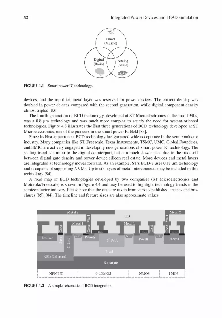
52 Integrated Power Devices and TCAD Simulation
devices, and the top thick metal layer was reserved for power devices. The current density was doubled in power devices compared with the second generation, while digital component density almost tripled [83].
The fourth generation of BCD technology, developed at ST Microelectronics in the mid-1990s, was a 0.8 µm technology and was much more complex to satisfy the need for system-oriented technologies. Figure 4.3 illustrates the first three generations of BCD technology developed at ST Microelectronics, one of the pioneers in the smart power IC field [83].
Since its first appearance, BCD technology has garnered wide acceptance in the semiconductor industry. Many companies like ST, Freescale, Texas Instruments, TSMC, UMC, Global Foundries, and SMIC are actively engaged in developing new generations of smart power IC technology. The scaling trend is similar to the digital counterpart, but at a much slower pace due to the trade-off between digital gate density and power device silicon real estate. More devices and metal layers are integrated as technology moves forward. As an example, ST’s BCD-8 uses 0.18 μm technology and is capable of supporting NVMs. Up to six layers of metal interconnects may be included in this technology [84].
A road map of BCD technologies developed by two companies (ST Microelectronics and Motorola/Freescale) is shown in Figure 4.4 and may be used to highlight technology trends in the semiconductor industry. Please note that the data are taken from various published articles and bro-chures [85], [84]. The timeline and feature sizes are also approximate values.
Metal 2 Metal 2
Metal 1Metal 1
STISTIN-Drift
Emitter P-bodyGate Gate Gate
P-epi
Substrate
N-LDMOSNPN BJT
NBL(Collector)
N-L
ink
Base
Cont
Cont
Cont
Cont
Via 1
Via 1
NMOS PMOS
STIP-well N-well
ILD
FIGURE 4.2 A simple schematic of BCD integration.
Power(Muscle)
Analog(Sense)
Digital(Brain)
FIGURE 4.1 Smart power IC technology.

53Smart Power IC Technology
BCD-3 (CMOS Based)
P Substrate
N+and P Buried Layers
N Epitaxial Layer
N+Deep Collector
P & N well
LOCOS Isolation
Tunnel Oxide
Gate 1
P body
Gate 2
LDD
Contact
N+and P+S/D
Metal 1 & 2
Metal 3
Passivation
BCD-2 (CMOS Based)
P Substrate
N+and P Buried Layers
N Epitaxial Layer
N+Deep Collector
P well
LOCOS Isolation
Gate
P body
N+S/D
P+S/D
Contact
Metal 1 & 2
Passivation
CMOS process ow
BJT process ow
Power device ow
BCD-1 (BJT Based)
P Substrate
N+Buried Layer
N Epitaxial Layer
P well
P+Junction Isolation
N+Deep Collector
P+Deep Body Gate
P Base
P–Drain Extension
N+Emitter
Contact
Metal
Passivation
FIGURE 4.3 Process flowchart of first three generations of BCD technology.
4.0µm ST BCD-1
ST BCD-2
ST BCD-3
ST BCD-5
ST BCD-6
ST BCD-8
Motorola/Freescale smartMOS 2
Motorola/Freescale smartMOS 3
Motorola/Freescale smartMOS 5
Motorola/Freescale smartMOS 7
Motorola/Freescale smartMOS 8
3.0µm
2.0µm
1.0µm
0.5µm
0.35µm
0.25µm
0.18µm
0.13µm 1980 1985 1990 1995 2000 2005 2010
ST BCD-4
FIGURE 4.4 BCD technology road map of two companies from 1980 to 2010. Timeline and feature sizes are approximate values [85] [84].

54 Integrated Power Devices and TCAD Simulation
4.3 SMART POWER IC TECHNOLOGY: INDUSTRIAL PERSPECTIVE
4.3.1 engineering groups oF A smArt power ic tecHnology
Semiconductor process technology is an important know-how for IDMs and foundries; each com-pany has its own process recipes for similar applications. This is like different chefs and recipes in different restaurants, with similar menus on the table. Process flows are different from company to company and are considered as trade secrets since it is an important differentiator just like one particular restaurant may add more salt and sugar for its pizza while another may opt for a lighter taste. The performance of analog and power IC depends heavily on the process technologies and manufacturing equipment.
Building a semiconductor process technology flow is a complicated task. Depending on past experience and technology advances, developing a new process technology generation (from planning stage to final certification) for analog and power IC usually takes a couple of years. Many groups of engineers with different technology backgrounds must work side by side to achieve this goal.
To give the reader some insight into the process, a simplified organization chart of engineering groups of smart power IC technology in a semiconductor company is given in Figure 4.5. Note that the exact names and functions differ from company to company, but the basic group functions are often similar. The arrows indicate the direction of support between groups and are for illustration purposes only. In a real company environment, the interactions between functional groups are much more complicated [39].
4.3.1.1 Process IntegrationThe process integration group acts as an interface between device design engineers and process/fab engineers. It spends a lot of its time supporting the device engineering, ESD, and compact modeling groups. Engineers in a process integration group will visit fabs from time to time and work with fab
Packaging
IC Design
DeviceDesign
TCADSupport
ProcessIntegration
CompactModeling
ProcessDesign KitReliability
ESD Design
Devices
Development
Engineering
Technology
FIGURE 4.5 Organization chart of a typical smart power technology development group.

55Smart Power IC Technology
engineers from individual process (e.g., CVD, implantation, diffusion) and provide process integra-tion solutions to device design engineers, ESD design engineers, and compact modeling engineers.
4.3.1.2 TCAD SupportThe TCAD support group basically uses commercially available TCAD tools or internal pro-prietary simulation tools to simulate the process flow and perform design of experiments (DoE) analysis with different device structures and process conditions. It is critical for TCAD software vendors to provide DoE functionality to enable batch processing and accelerate the development cycle. For larger companies, TCAD simulation is performed with a dedicated group of engineers, whereas smaller companies generally do not distinguish TCAD engineers from device engineers. TCAD simulation plays an important role throughout the process technology development cycle as TCAD tools can help explain important physics that are hard to visualize or calculate manu-ally; well-tuned simulators may even be able to predict the device performance before tape-out. The TCAD support group needs to support device design, compact modeling, ESD design, and process integration.
4.3.1.3 Compact ModelingCompact modeling groups are very important for IC designers. Sometimes an inaccurate compact model can lead to a design failure. This is especially true for novice designers who rely too much on simulations rather than experience. Even though there are excellent models like BSIM4, PSP, and VBIC, the model parameters usually need to be determined before they can be used. For BCD technology, LDMOS also needs a more complicated model that is structure dependent. Unlike the fabless companies, in which the device models are provided by the foundries in the process design kit (PDK), IDMs, or foundries themselves have very different process flow and device structures for analog and power ICs. Even within the same company, an older 0.35 µm technology is by no means the same as the latest 0.13 μm technology in terms of compact models and their parameters. Compact modeling groups will work closely with device design engineers, since they are the ones who will provide device types, structures, and test wafers for parameters extraction. Compact mod-eling groups need to work closely with PDK groups to provide simulation tools for IC designers.
4.3.1.4 Device DesignThe device design group is often a core group in the process technology development. Engineers in this group will work closely with IC design engineers to determine the next generation of process technology on the road map. A good practice should always look more than a few years ahead of time. However, since the scaling of power ICs is not keeping pace with their digital counterparts, an overly agreesive design without market and cost considerations is not a good practice for analog and power IC development. Besides device structure and process flow design, device design engi-neers will generally coordinate with almost all other groups to define the technology road map. The most important of these other groups is process integration; device designers need to get constant feedback from process integration engineers to run process splits and optimize the process recipe.
4.3.1.5 ESD DesignThe ESD design group directly supports IC designers to meet their electrostatic discharge require-ments as ESD protection devices have special structures that may be different from any other devices in use for the IC. Engineers in the ESD group utilize the layers from the process flow to build the ESD devices. Sometimes, one or more dedicated layers need to be created especially for ESD devices; however, this should be avoided whenever possible to save on cost. Different models are used in ESD tests to mimic different situations and ESD events, such as the human–body model (HBM), machine model (MM), and charged-device model (CDM).

56 Integrated Power Devices and TCAD Simulation
4.3.1.6 Process Design KitThe PDK group is a CAD support team. Engineers in this group provide all technology develop-ment engineers with files that contain standard cell libraries, design rule checking (DRC), device compact models, and parameterized cells (Pcells) for layout. These files are meant to be used in circuit-level CAD tools like Cadence by the device and IC design engineers.
4.3.1.7 IC Design GroupThe IC design group is at the heart of any analog/power IC company and can be regarded as the cus-tomer of the whole technology development group. Analog and power IC designers need to interact with process development engineers; this is very different from digital design where IC designers rarely care about what a transistor looks like or how the device size or layout orientation can impact on the device performance.
4.3.1.8 Reliability GroupThe reliability group deals with wafer-level and package-level reliability tests. For new technology to be certified as mature, accelerated wafer-level tests need to be carried out. The standard tests include time-dependent dielectric breakdown (TDDB) to qualify the gate oxide, hot carrier injec-tion (HCI) to test the long-term physical parameter drift, and electromigration (EM) to exam the robustness of the metal interconnect, vias, and contacts. Package-level tests like high-temperature operating life (HTOL) and IDDQ (test supply current Idd leakage in the quiescent state for CMOS) may be performed as well. The reliabilty group meets with engineers from other groups to make sure the technology being developed meets the standards for the intended applications, which is important for final technology certification.
4.3.1.9 PackagingPackaging is becoming ever more important with novel packaging methods constantly being devel-oped. System in package (SIP) is an emerging trend for integration of power management in a single package. Compared with system on chip (SOC), SIP provides more flexibility, faster time to market, lower research and development (R&D) costs, and thus lower production costs for many applica-tions [86]. However, SIP also has disadvantages such as internal parasitic effects and the difficulty of assembling multiple chips.
4.3.2 smArt power ic tecHnology development Flow
Analog and power IC process technology development is a time-consuming project even if con-sumer electronics with its narrower time window is driving the process. A typical turnaround time for an 8-inch 0.25 µm power IC fabrication is at least a month or two; unless one can ensure as few test vehicles as possible, the total development time for a new generation of power IC process will be over two years. Looking a bit more than a few years ahead is always necessary as long as the estimated chip cost is under control. A typical process technology development flow is shown in Figure 4.6. In the following sections, each step will be explained in detail.
4.3.3 plAnning stAge
The very first and most critical step of a new technology development is the planning stage: the entire project cannot be carried out smoothly without proper planning. Engineers should get advice and guidance from the business and strategy department to make sure they are targeting the right

57Smart Power IC Technology
applications. At this stage, engineers need to foresee future needs, usually a few years ahead, to make sure the new technology is neither too advanced (which may be costly) nor too conservative (which will make it obsolete even before release). Engineers need to understand the applications of the new technology since different applications will require different technologies. For example, standard automotive application generally requires higher voltage (> 80 V) than wireless communi-cation application (~20 V). IGBT driver IC for hybrid cars usually requires HVIC with over 700 V of breakdown voltage capability.
The proper selection of technology node (i.e., the feature size) is critical. For power IC technolo-gies, there is no equivalent to Moore’s law [87] guideline of improvement found in advanced CMOS technologies. It is true that with smaller technology feature sizes a higher logic device density can be achieved and a larger number of gates can be packed onto the same die. However, the largest por-tion of the chip is often occupied by power devices that are much less influenced by scaling trends. There is always a trade-off between higher gate density and chip cost so a more advanced node does not necessarily mean a lower cost per chip. The choice of wafer is determined by several aspects. For example, a silicon-on-insulator (SOI) wafer may be good for better immunity of cross-talks but are very expensive for cost sensitive applications such as power management systems. Table 4.1 lists several considerations for the planning stage.
4.3.4 process integrAtion And device design
The device design stage is the core stage that defines the road map of smart power IC technol-ogy. Since there are usually many device types in a smart power IC technology, engineers take ownership of devices, and most of the time advanced power devices such as LDMOS with high breakdown voltages are assigned to the most senior engineers as they require years of experience. Analog and digital MOSFETs have fewer considerations and are usually assigned to relatively
Planning Stage
Process Integrationand Device DesignTCAD Simulation
PDK Support
PDK Support
Layout for Test VehicleMore TestVehicles?
Tape-out andFabrication
Wafer Level Testing
CompactModeling
ReliabilityTest
IC Design
Packaging and Test
ESD Design
FIGURE 4.6 Simplified process flow of analog and power technology development.
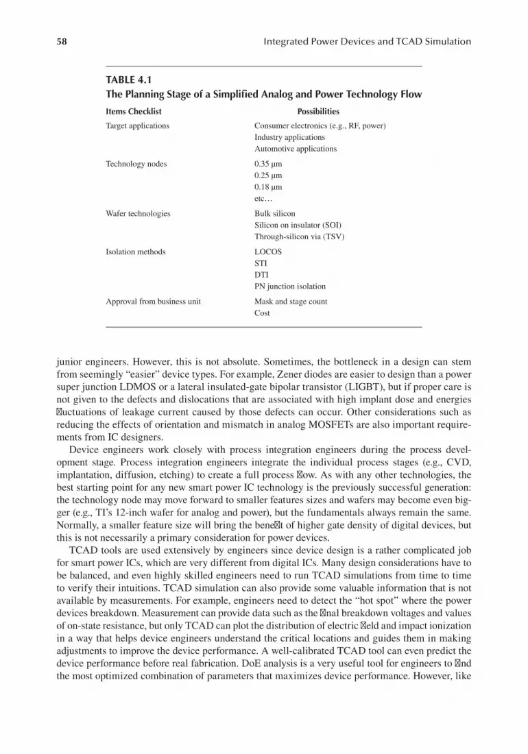
58 Integrated Power Devices and TCAD Simulation
junior engineers. However, this is not absolute. Sometimes, the bottleneck in a design can stem from seemingly “easier” device types. For example, Zener diodes are easier to design than a power super junction LDMOS or a lateral insulated-gate bipolar transistor (LIGBT), but if proper care is not given to the defects and dislocations that are associated with high implant dose and energies fluctuations of leakage current caused by those defects can occur. Other considerations such as reducing the effects of orientation and mismatch in analog MOSFETs are also important require-ments from IC designers.
Device engineers work closely with process integration engineers during the process devel-opment stage. Process integration engineers integrate the individual process stages (e.g., CVD, implantation, diffusion, etching) to create a full process flow. As with any other technologies, the best starting point for any new smart power IC technology is the previously successful generation: the technology node may move forward to smaller features sizes and wafers may become even big-ger (e.g., TI’s 12-inch wafer for analog and power), but the fundamentals always remain the same. Normally, a smaller feature size will bring the benefit of higher gate density of digital devices, but this is not necessarily a primary consideration for power devices.
TCAD tools are used extensively by engineers since device design is a rather complicated job for smart power ICs, which are very different from digital ICs. Many design considerations have to be balanced, and even highly skilled engineers need to run TCAD simulations from time to time to verify their intuitions. TCAD simulation can also provide some valuable information that is not available by measurements. For example, engineers need to detect the “hot spot” where the power devices breakdown. Measurement can provide data such as the final breakdown voltages and values of on-state resistance, but only TCAD can plot the distribution of electric field and impact ionization in a way that helps device engineers understand the critical locations and guides them in making adjustments to improve the device performance. A well-calibrated TCAD tool can even predict the device performance before real fabrication. DoE analysis is a very useful tool for engineers to find the most optimized combination of parameters that maximizes device performance. However, like
TABLE 4.1The Planning Stage of a Simplified Analog and Power Technology Flow
Items Checklist Possibilities
Target applications Consumer electronics (e.g., RF, power)Industry applicationsAutomotive applications
Technology nodes 0.35 μm0.25 µm0.18 μmetc…
Wafer technologies Bulk siliconSilicon on insulator (SOI)Through-silicon via (TSV)
Isolation methods LOCOSSTIDTIPN junction isolation
Approval from business unit Mask and stage countCost

59Smart Power IC Technology
any other software tools, engineers should use their own experience and insights when designing a process recipe or device structures: blindly following simulation results can lead to off-target designs and frustration.
Table 4.2 is an outline of some important considerations during the device design and process development stage [39]. While this table provides a starting list, there are many other considerations in the real world. Some of these can be unexpected, such as performance variations from lot to lot and die to die that come from the fabrication equipment in spite of the best efforts of device and process engineers.
TABLE 4.2Process Integration and Device Design Considerations
Type of devices Digital MOSFETs (1.5 V); Analog MOSFETs (3.3 V); Power MOSFETs (> 12 V)
Zener diode (5 V); HV diode (45 V); BJTs
Capacitors (poly-poly capacitor, metal-insulator-metal capacitor)
DRC test shapes, etc…
Resistors (diffused, poly)
Possible improvement over last generation Higher breakdown voltage; lower on-state resistanceBetter safe operating area (SOA); more robust ESD protection
Better temperature coefficient and voltage coefficient for resistors
Higher current gain for BJTs; better power handling capability for power devices
Lower substrate leakage with suppressed minority carrier injection
Higher capacitor density
Higher digital gates density with more advanced technology node
Reliability test shapes for TDDB, HCI, NBTI, and EM
Metal interconnect schemes for large power LDMOS to reduce the metal debiasing effect
Thick copper or gold last metal layer for devices to handle larger current flow
Fuse/anti-fuse/NVM for trimming
TCAD simulation Various device structures are simulated with TCAD process and devices simulators to predict and verify performance and to help designers find the best parameters for both process recipes and device structures
Process integration steps like buried layer, well implants, and STI can be simulated to help reduce turnaround time
Important performance parameters like threshold voltage and breakdown voltage can be simulated
Calibrated data from previous technology are reused so that engineers can have more confidence with the simulations
DoE to simulate and guide process splits

60 Integrated Power Devices and TCAD Simulation
4.3.5 lAyout, tApe-out, FABricAtion, And test
After device and process design, engineers can now lay out the device test structures using layout tools such as Cadence Virtuoso. Often, engineers will place all types of devices including capaci-tors and resistors onto the same test wafer. Many design variations have to be considered for the devices, such as LDMOS with rectangle or racetrack shapes, analog MOSFETs with different ori-entations, digital MOSFETs with minimum feature sizes, and various capacitors. Before tape-out, a design rule checking (DRC) is normally performed to make sure that all the layouts obey the design rules. These design rules are made by collaboration between the various function groups, and many of them are derived from past experience and measurement data from experimental device structures. For a new generation of design, the DRC test structures should also be placed onto the test wafer. Obeying the design rules can help improve process yield by checking impor-tant parameters such as minimum width and spacing between devices. For readers that are not familiar with the word tape-out, it means to deliver the finished design masks to the fab engineers to make photomasks. The word is derived from the early days when the enlarged “artwork” for the photomask was “taped out” manually using black line tape and adhesive-backed die cut ele-ments on sheets of polyester PET film [88] [89]. For most design engineers, the busiest months of the year are just before tape-out: since the mask-making process is very costly, they have to make sure everything they draw is correct according to the best of their knowledge. In addition to the costs involved, the turnaround time can be in months, so errors at this stage can introduce delays of several months for the next tape-out, which is unacceptable for time-sensitive products like cell phone chips.
After tape-out, engineers can relax a little bit while waiting for the silicon wafers to come back. In the meantime, the compact modeling group can ramp up to build some “paper models” based on their past experience and TCAD simulations. During the fabrication period, process integration engineers give feedback based on the current status of the process and may perform some tests by withdrawning some wafers during specific stages. TEMs or SEMs are taken and send back to device design engineers to verify the design or process if something unusual happens.
After the fabrication is finished, some of the wafers are held back by fab engineers for scribe grid process control (SGPC) tests and data gathering. The SGPC test structures are located at the unused scribe lines between dies, redundant locations where the wafer is cut into separate dies for packaging. These test structures are prepared by device engineers, and they are very important to monitor and control the process. Usually, automatic wafer-level tests are performed, and statistical data are col-lected and analyzed using software tools such as JMP from the SAS Institute [90]. After the SGPC tests, wafers are shipped back to the device engineers for further tests and characterization. Compact modeling engineers can use the measurement data to extract parameters for compact models used by IC designers.
Most of the time, one test vehicle is not enough, since new issues always pop up; multiple test vehicles (test mask sets) are often necessary. In that case, more tape-outs are carried out before finalizing the process technology and device designs.
4.3.6 reliABility And QuAliFicAtion
Reliability engineers are responsible to make sure the devices designed and process technologies meet the contingent requirements for various applications. Note that reliability is not the same as quality. Reliability is something measured over the long term as a semiconductor device’s per-formance gradually degrades over time depending on the environment and working conditions. Typical reliability tests include the TDDB, HCI, EM, and NBTI.
Gate dielectric materials can suffer a sudden breakdown after being subject to electrical stress over a prolonged period of time; depending on the gate oxide’s quality, the exact time to breakdown varies from device to device. The mechanism for this breakdown is the formation of a conductive

61Smart Power IC Technology
path within the thin gate oxide due to stress: many models [91] [92] [93] have been proposed by researchers in this field to analyze this phenomenon. For example, researchers from the University of California at Berkeley in [93] proposed an anode hole injection (AHI) model for reliability pro-jection of oxide. Ultimately, the exact causes of oxide failure and the proper models to use to predict oxide reliability are still under debate. In industry, time to breakdown is projected with the help of accelerated measurements under high-voltage and high-temperature conditions. These tests often involve the extrapolation of the dielectric lifetime for test structure using scaling coefficients to account for area, temperature, and voltage. The Weibull distribution and percolation theory are used for the cumulative fail assessment [93]. Figure 4.7 shows a typical cumulative fail accelerated test result for TDDB.
HCI affects all MOSFETs. In this process, electrons and holes can gain sufficient kinetic energy to overcome a potential barrier necessary to break an interface state [94]. For digital and analog MOSFETs, hot carriers can tunnel through the thin gate oxide and contribute to gate leakage current. In LDMOS with STI in the drain-drift region, hot carriers injected and trapped in the STI corner can alter the device performance. For example, researchers have found the on-state resistance can be modified by hot carrier injection [95].
EM is the gradual movement of ions in a conductor due to the momentum transfer between conducting electrons and diffusing metal atoms [96]. Modern power IC technologies use copper instead of aluminum to reduce resistance from the metal interconnects. It also turns out that copper has better electromigration robustness than aluminum or Al/Cu alloy; however, while the advantage is significant it is not as great as originally anticipated [97]. Like TDDB, electromigration tests are routinely carried out at elevated temperatures to make sure it meets the desired specs.
Other tests like NBTI for PMOS, plasma-induced damage or antenna effect [98], and IDDQ are typically carried out.
4.3.7 survey oF current smArt power tecHnology
A brief survey (as of the year 2013) of smart power technology foundry providers is shown in Table 4.3. Most foundries have multiple technology offerings for different power IC applications. For example, TSMC provides both lower voltage (60 V) and high voltage (800 V) services [99].
Gate Stress at 15 V, 150 C10080
60
40
20
108
6
40.1 0.2 0.4 0.6 0.8
Time to Failure (h)
Cum
ulat
ive F
ail %
(Wei
bull)
1 2 4 6 8 10
FIGURE 4.7 A typical cumulative fail reliability assessment using the Weibull distribution.

62 Integrated Power Devices and TCAD Simulation
4.4 SMART POWER IC TECHNOLOGY: TECHNOLOGICAL PERSPECTIVE
Nowadays, advanced manufacturing has pushed the feature size from submicron to nanoscale. The latest Intel Ivy–bridge chip uses 22 nm Tri-gate technologies that brings 3D concepts to advanced CMOS fabrication for the first time. With improvements in extreme ultraviolet (EUV) lithography and other innovations, the semiconductor technology is aiming at 14 nm in a few years’ time, so it will not be long before we reach the end of scaling where Moore’s law is no longer valid. “More than Moore” is rapidly picking up momentum, with smart power IC technology being a typical applica-tion of this concept. As mentioned before, the feature size shrinking for smart power technology is several generations behind due to the trade-off between cost and performance so there is still lots of room for improvement. Today’s smart power technology uses technology with a feature size of 0.13 μm and above. Some companies are still using feature sizes greater than 1 μm for high-voltage ICs since only a small number of digital gates are required.
A comparison of CMOS technology and smart power technology as of the year 2013 [39] is given in Table 4.4. A variety of device types like the passives (resistors and capacitors) are available for smart power technology, which makes system-on-chip applications possible. However, inductors and transformers are very difficult to integrate on the chip: they are either stand-alone on the PCB board or integrated in the package by advanced packaging technologies.
4.4.1 devices For smArt power tecHnology
In advanced CMOS technology development, the ability to realize continued scaling without jeopardizing leakage and reliability is the key to success. Novel technologies such as high-k
TABLE 4.3A Brief Survey of Smart Power Technology Foundry Providers
Smart Power IC Technology Nodes (µm)
Voltage Rating (V) (for PIC)
High-Voltage IC Technology Nodes (µm)
Voltage Rating (V) (for HVIC)
TSMC [99] 0.18 to 0.35 12 to 60 0.5 to 1.0 500 to 800
UMC [100] 0.18 to 0.60 12 to 120 0.5 to 0.6 700 to 800
Global Foundry [101] 0.13 to 0.18 (BCDlite) 5 to 60 -
SMIC [102] 0.13 to 0.35 20 to 100 - 600
TABLE 4.4Comparison between CMOS Technology and Smart Power IC Technology as of 2013
CMOS Technology Smart Power Technology
Feature size 45 nm and below 0.13 µm and above
Wafer size Mostly 12 inch 8 inch and below
Device types NMOS and PMOS LDMOS, BJTs, diodes, capacitors, resistors
Isolation STI STI, LOCOS, DTI, P-N Junction
Gate insulators Oxide or high-K materials Oxide
Gate materials Metal Polysilicon
Strain engineering Available Not available
63Smart Power IC Technology
materials and metal gate stacks, 3D current flows with FinFET-like structures, stress and strain to increase carrier mobility, and phase-shifted masks and immersion lithography have driven silicon technology into the nanoregion. However, CMOS technology has only two basic device types (NMOS and PMOS), whereas a smart power technology may have over a dozen of device types. The considerations of smart power technology development are therefore quite different from those of CMOS. Leakage current is still a big consideration for smart power applica-tions, but gate leakage is less of a concern due to the much thicker oxide layers used in this technology. In the context of smart power ICs, leakage refers to the substrate leakage current that should be suppressed to prevent cross-talk between devices. Since both power devices and digital devices coexist on the same chip, improving the isolation between devices is absolutely critical.
Further challenges for smart power ICs depend on the specific application. For example, an LDMOS may be used in high-side applications, where the substrate is still grounded while source and body are lifted to high potential; in that case, preventing the influence of the substrate depletion on the active devices is an important task. Another example is the electron-hole plasma generated during the on-state of LIGBT, which can generate cross-talk between high-voltage devices or between high-voltage and low-voltage devices. Special precautions are needed if one would like to take advantage of the lower on-resistance of LIGBT over LDMOS. Many other such examples exist and for every single case; multiple device technology parameters need to be optimized at the same time.
Table 4.5 gives list of devices used in smart power technology [39]. The requirements on these devices and the choice of technology depend on the intended application. Design considerations and optimizations will be discussed in the following sections.
4.4.2 design considerAtions For smArt power ic tecHnology
4.4.2.1 Power MOSFETsFor power devices, breakdown voltage is one of the first design parameters to be considered; dif-ferent applications require different breakdown values. For real-world applications, voltage spikes need to be considered so that a 12 V application may require a power device rating of 20 V and above. Additionally, a 20 V power LDMOS does not mean the breakdown voltage is exactly 20 V; quite often an extra 20% or 30% safety margin is added to account for device degradation and ensure the device meets specifications over its entire lifetime.
In power electronics, N-type LDMOS is often preferred over P-type LDMOS because electrons have higher mobility than holes in silicon; this means the nLDMOS will have a lower specific on-state resistance. For power device engineers, breakdown voltage and specific on-state resistance are almost always a trade-off, and meeting both goals at once is not easy. Over the past decades both RESURF (Reduced Surface Field) and Super Junction concepts were widely used, especially for
TABLE 4.5Typical Devices in a Smart Power Technology
Categories Devices
Digital NMOS and PMOS
Analog NMOS and PMOS, BJT, Zener diode
Power LDMOS, BJT, LIGBT, power diode
Capacitors MOS capacitor, double-poly capacitor, metal-insulator-metal capacitor
Resistors Diffused resistor, poly resistor
Trim Fuse, anti-fuse, NVM

64 Integrated Power Devices and TCAD Simulation
high voltage ICs (> 100 V for RESURF, > 300 V for Super Junction). Both RESURF and Super Junction use the same charge coupling effect; RESURF is about two-dimensional optimization that can be applied multiple times (e.g., multiple-RESURF), whereas Super Junction is more about three-dimensional effects and usually consists of alternating N and P-regions in a direction perpen-dicular to the channel.
Gate oxide integrity is also important. For power devices, a high voltage is usually applied to the gate (> 5 V) to fully turn on the device so that low on-state resistance is achieved. However, high-voltage and high-temperature stresses on the gate oxide over a prolonged period can cause gradual oxide degradation and an eventual rupture. The previously mentioned TDDB test is an accelerated method of determining the oxide quality and its long-term reliability. Modern smart power tech-nologies use different oxide thicknesses for different device categories (power, analog, and digital) so individual TDDB tests are necessary for every oxide thickness.
Other considerations of power devices include its energy capability, safe operating area (SOA), and thermal runaway (second breakdown) prevention. The suppression of the parasitic BJTs in power LDMOS is a very important design consideration; since these parasitic BJTs can prove cata-strophic for power devices, a lower resistance path in the P-body region of LDMOS is often used to reduce this risk.
4.4.2.2 LIGBTsFor power switching applications with high current density, the on-resistance of an LDMOS will be too large unless the device size is very large; LIGBTs are usually used to avoid this problem [103] [104] [105] [106]. By using conductivity modulation in the structure, the on-resistance of an LIGBT can be many times lower than that of an LDMOS. For the same current and voltage rating, the chip size of an LIGBT can also be many times smaller than that of an LDMOS, but there is a trade-off between on-resistance and turnoff time: the longer turnoff time of an LIGBT is due to the existence of minority carriers (related to the conductivity modulation), which reduce the on-state resistance of the device significantly. Therefore, for low current density and fast switching applications, LDMOS should be used; for high current density and slow switching applications, LIGBTs are the better choice.
In terms of breakdown voltage design, both structures are similar except that an N buffered layer is used in LIGBT to prevent premature breakdown at the anode. There are two unique design parameters in LIGBT, which are not a major concern for LDMOS. The first one is the device latch-up due to the turn-on of the P+ anode/N-drift/P-body/N+ cathode parasitic thyristor. Once this parasitic thyristor latches on, gate turnoff of the device will not be possible. The turn-on mechanism of LIGBT latch-up is similar to the second breakdown mechanism for LDMOS. The difference is that LIGBT latch-up might cause only loss of gate control and not necessarily a catastrophic failure as in LDMOS. However, both devices require the P-body doping to be high enough to provide a low resistive path for the hole current. The second major concern for the LIGBT is the spreading of the minority carriers in the substrate. As LIGBTs are integrated with the control circuits in power IC applications, spreading of the minority carriers might cause cross-talk between power devices [107] or between power and low-voltage devices (e.g., CMOS and BJT [108]). Problems such as CMOS latch-up in neighboring circuits might be induced if proper precautions are not taken. Plasma con-finement during system operation [109] and effective isolation between power devices and low-voltage devices were reported as effective methods for cross-talk prevention [110].
4.4.2.3 Analog Active DevicesAnalog NMOS and PMOS devices mostly work in the saturation region, so important consider-ations for these devices include transconductance (Gm), output resistance (Rout), transistor matching, off-state current, and noise. Device orientation (channel orientation) may cause discrepancy for device parameters like threshold voltage (Vt). Even a small difference in Vt will cause a mismatch problem. For BJTs, one needs to consider the current gain, early voltage, matching, and noise.

65Smart Power IC Technology
Diode characteristics will depend on the kind of behavior desired. Power diodes have similar structures and voltage ratings as power LDMOS. Zener diodes, on the other hand, have heavily-doped P- and N-regions and are often meant to work under reverse bias to clamp and protect the power device gates from voltage spikes. The breakdown voltage of these devices is usually low. In fact, for Zener diodes with breakdown voltage up to 5.6 V, the Zener effect is the predominant effect and shows a marked negative temperature coefficient. Above 5.6 V, the avalanche effect becomes predominant and exhibits a positive temperature coefficient [111]. Strictly speaking, Zener diodes with breakdown voltage above 5.6 V are not pure Zener diodes.
4.4.2.4 ResistorsDepending on the application requirement, the integrated resistors can be diffused-well resistors or poly resistors. The sheet resistivity is determined by the process and by the doping type (N+ or P+). Temperature and voltage coefficients are two important considerations for resistors: in general, poly resistors have better accuracy and a lower voltage coefficient than diffused resistors, but diffuse resistors are a good choice if a large sheet resistance value is required.
4.4.2.5 CapacitorsThere are several types of capacitors in a smart power IC technology: the most widely used are MOS gate capacitors (MOS-caps) and poly-insulator-poly (PIP or double-poly) capacitors. PN junc-tion capacitors and metal-insulator-metal (MIM) capacitors are used as well. The voltage ratings for MOS caps are always lower than that of double-poly capacitors due to thin MOS gate oxide and thick poly to poly insulator, but MOS caps have higher capacitor density (Farads per unit area). The linearity, temperature, and voltage coefficients are also important design parameters.
4.4.2.6 Voltage and Frequency TrimsFuse, anti-fuse, and or NVM are used as voltage and frequency trims in analog ICs. Since the accu-racy of an analog IC is limited by the realities of the manufacturing process, trimming is often used to make adjustments to the IC after it is fabricated. This is typically done at wafer level on each indi-vidual die but may be performed on the die after packaging [112]. There are several ways to achieve anti-fuses in smart power IC, the technical details of which are beyond the scope of this book.
4.4.2.7 Logic/Digital NMOS and PMOSFor smart power IC technology, the most important aspect for logic design is the gate density. A 0.25 µm technology can pack more than 250 K gates for the digital part [113]. Other design consid-erations include the cost due to the added complexity of state-of-the-art CMOS process and noise isolation to protect the digital circuits from the analog and power devices.
4.4.2.8 System-Level Design and Fabrication ConsiderationsIn summary, the following should be considered when doing system-level design:
1. Substrate injection isolation 2. Embedded parasitic BJTs 3. Noise immunity 4. Heat dissipation 5. High-voltage ESD
In practice, many other considerations related to physical effects of the fabrication must be con-sidered. This includes the loading effect, which is caused by mask pattern density variations and the ion implantation proximity effect. The net result of these effects is a variation of device param-eters and IC performance from die to die, from wafer to wafer, and from lot to lot. For economic
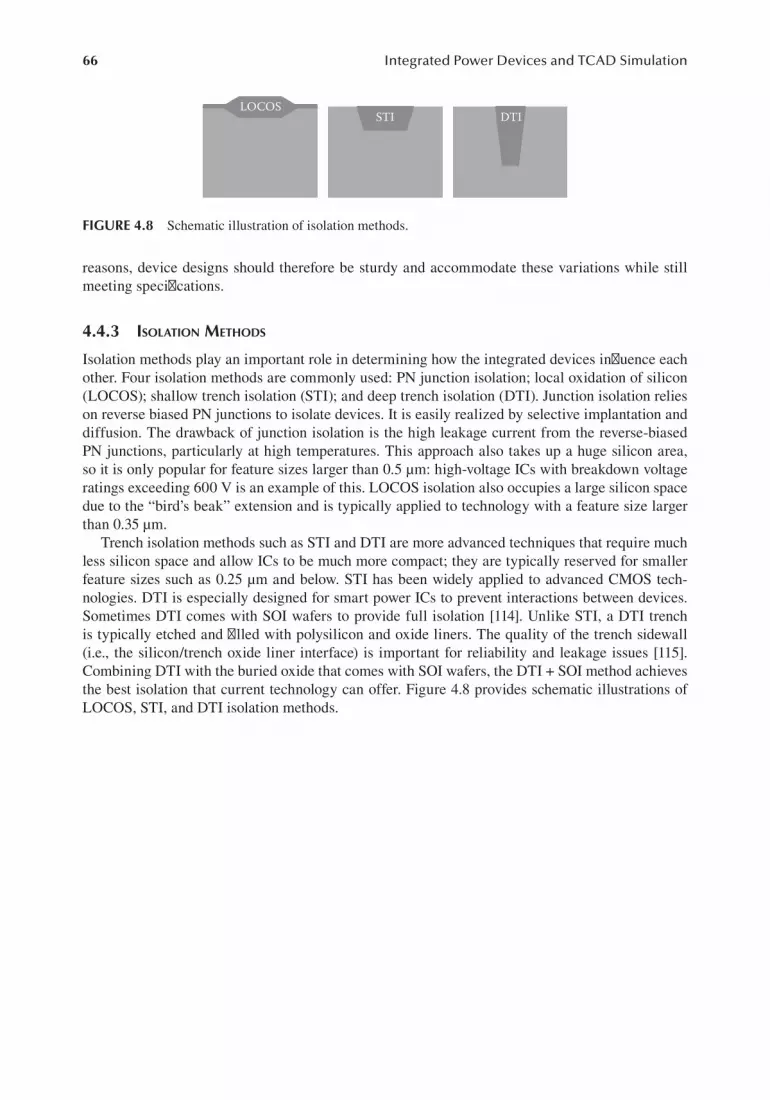
66 Integrated Power Devices and TCAD Simulation
reasons, device designs should therefore be sturdy and accommodate these variations while still meeting specifications.
4.4.3 isolAtion metHods
Isolation methods play an important role in determining how the integrated devices influence each other. Four isolation methods are commonly used: PN junction isolation; local oxidation of silicon (LOCOS); shallow trench isolation (STI); and deep trench isolation (DTI). Junction isolation relies on reverse biased PN junctions to isolate devices. It is easily realized by selective implantation and diffusion. The drawback of junction isolation is the high leakage current from the reverse-biased PN junctions, particularly at high temperatures. This approach also takes up a huge silicon area, so it is only popular for feature sizes larger than 0.5 µm: high-voltage ICs with breakdown voltage ratings exceeding 600 V is an example of this. LOCOS isolation also occupies a large silicon space due to the “bird’s beak” extension and is typically applied to technology with a feature size larger than 0.35 µm.
Trench isolation methods such as STI and DTI are more advanced techniques that require much less silicon space and allow ICs to be much more compact; they are typically reserved for smaller feature sizes such as 0.25 µm and below. STI has been widely applied to advanced CMOS tech-nologies. DTI is especially designed for smart power ICs to prevent interactions between devices. Sometimes DTI comes with SOI wafers to provide full isolation [114]. Unlike STI, a DTI trench is typically etched and filled with polysilicon and oxide liners. The quality of the trench sidewall (i.e., the silicon/trench oxide liner interface) is important for reliability and leakage issues [115]. Combining DTI with the buried oxide that comes with SOI wafers, the DTI + SOI method achieves the best isolation that current technology can offer. Figure 4.8 provides schematic illustrations of LOCOS, STI, and DTI isolation methods.
LOCOSSTI DTI
FIGURE 4.8 Schematic illustration of isolation methods.

67
5 Introduction to TCAD Process Simulation
In previous chapters, we discussed power electronics systems and integrated circuits (ICs) the semi-conductor industry in general, and the fundamentals of smart power IC technology by following a top-down approach. Starting from this chapter, we are getting into the lowest and most fundamental level of device engineering. Before we explain the integrated power devices that are used in today’s power IC industry, we need to prepare the readers with some basic knowledge of technology com-puter-aided design (TCAD) simulation, since these will be used extensively from Chapters 7 to 10. TCAD simulations can be divided into two categories: process simulation and device simulation. This chapter discusses process simulation, and device simulation will be the topic of Chapter 6.
5.1 OVERVIEW
In the past decades, semiconductor manufacturing has gotten increasingly complex. The cost of development is rising sharply in spite of the ever-decreasing unit price of semiconductor chips. Driven by consumer electronics, electronic gadgets’ lifetime and time to market are getting shorter and shorter. The traditional “trial and error” methodology is no longer feasible due to cost and time constraints. Computer-aided design (CAD) is universally accepted for design and development of ICs; for semiconductor process and device design, a special tool within this CAD category is called TCAD.
TCAD is widely used in industry and research institutes to simulate semiconductor manufac-turing process technology; a different set of tools is also used to study the electrical, thermal, and optical properties of semiconductor devices. This chapter and Chapter 6 focus on general TCAD simulation applications. Since a detailed explanation of the physical models implemented in TCAD software can be found in most commercial software manuals, this chapter and Chapter 6 concen-trate on the most useful and important aspects of TCAD simulation that an ordinary TCAD user will encounter for power devices. Advanced readers can refer to [39] for detailed explanations.
Process simulation is similar to virtual manufacturing of semiconductor devices. It starts with a wafer substrate and simulates most of the important process steps like ion implantation, deposition, oxide growth and diffusion, and etching. A modern process simulator can simulate both front-end of the line (FEOL) and back-end of the line (BEOL) processes with reasonable accuracy. This chap-ter gives the reader an introduction of process simulation based on one of the most popular industry standard process simulators: Suprem IV, which was originally developed by Stanford University.
A simplified process simulation flowchart is illustrated in Figure 5.1.
5.2 MESH SETUP AND INITIALIZATION
Process simulation always starts with mesh definition and initialization. Let us first take a look at a simple example:
line x location = 0.00000 spacing = 0.250000 tag = leftline x location = 5.00000 spacing = 0.250000 tag = right
line y location = 0.00000 spacing = 0.1 tag = topline y location = 5.00000 spacing = 0.5 tag = bottom

68 Integrated Power Devices and TCAD Simulation
region silicon xlo = left xhi = right ylo = top yhi = bottomboundary exposed xlo = left xhi = right ylo = top yhi = topboundary backside xlo = left xhi = right ylo = bottom yhi = bottom
initialize boron conc = 1.0e15 orient = 100structure outfile = sub.str
This example simulates a silicon substrate with a width of 5 µm (x direction, pointing to the right) and a thickness of 5 µm (y direction, pointing downward). The simulation result is shown in Figure 5.2.
Every process simulation starts with mesh definition, and a well-defined mesh can increase simu-lation accuracy and efficiency. A rule of thumb is denser mesh required at locations where a large gradient of doping concentration exists, where contacts will be defined or at particularly interesting locations like a MOSFET channel region. The “line” command specifies the location of a mesh line. Vertical and horizontal lines are used, and the software divides the device into a triangular mesh by splitting the rectangles defined by these lines. This means that at the very least two lines need to be defined to enclose the meshed area. We note that in the Stanford convention for Suprem, the positive Y direction is pointing downward into the substrate.
An additional parameter called “spacing” is used to automatically put mesh lines between the specified lines of the input file. While additional mesh lines can always be added manually, using spacing allows mesh lines to be added in a smooth manner. The spacing of the supplemental lines will vary geometrically from one end of the interval to the other [116] so that the specified
Material NumberSi
5 +X432105
4
3
2
1
0–Y
FIGURE 5.2 Process simulation result of a simple silicon substrate.
Mesh Setup
Initialize
Main Process
Export
Deposition Implantation Diusion Etching
FIGURE 5.1 Simplified process simulation flowchart.

69Introduction to TCAD Process Simulation
spacing value (in microns) is used at both ends. Additional lines are then introduced using a smoothing procedure so that adjacent lines intervals have a ratio no greater than 1.5.
Another parameter in the line command is “tag,” which allows user to specify which line com-mand has one of the four boundaries: left, right, top and bottom. These tags will be used in the “region” and “boundary” commands to define the initial simulation conditions.
The “region” command should follow “line” command to set the rectangular mesh boundary. The string value given in the “tag” can be used to set the parameters of “xlo,” “xhi,” “ylo,” and “yhi,” which are abbreviations of the low point of x, high point of x, low point of y, and high point of y. At least one material should be specified for one particular region. In this example, silicon is the only material within the mesh boundary.
The “boundary” command is used to specify what conditions to apply at each surface in a rect-angular mesh. One of three boundary conditions can be chosen for a particular surface: reflect-ing, exposed, or backside. In this example, the first boundary command set the top surface of the substrate as exposed. Materials are deposited only on exposed surfaces. Impurity pre-deposition also happens at exposed surfaces, as does defect recombination and generation [116]. The second boundary command defines the bottom of the substrate as backside. Backside surfaces roughly cor-respond to a nitride-capped or oxide-capped backside; defect recombination and generation happen here. Reflecting surfaces correspond to the sides of the device and are also good for the backside if defects are not being simulated: this is the default setting for all surfaces.
With the mesh and boundaries defined, we can now initialize the process simulation. The initialize statement sets up the mesh and also initializes the background doping concentration and wafer surface orientation. In this example, the substrate has an initial boron doping concentration of 1E+15 cm–3 and wafer surface orientation is (100).
Finally, the “structure” command allows the user to save the file to a certain file format so that the structural information such as material and net doping can be visualized. The saved data can also be used as a restart point for future simulations.
5.3 ION IMPLANTATION
The most widely used doping technique in modern integrated circuits technology is ion implan-tation, in which ionized dopants atoms are accelerated by an electrostatic field that then strikes and penetrates the target material. The dose can be controlled by controlling the ion current and the profile depth is controlled by the implantation energy which can be adjusted through the field strength. Since dose and depth can be adjusted electrically, ion implantation is highly controllable and reproducible [117] [118]. The implanted ions cause implantation damage by displacing the wafer atoms (defects generations) or by creating clusters and precipitates: a subsequent thermal annealing is therefore necessary to heal as much of the implantation damage as possible. A rapid thermal anneal (RTA) at very high temperatures can be used to repair the damage with minimum dopant diffusion. Ion implantation into a single crystal causes another problem due to the anisot-ropy of the target: along the major crystal axes, the implanted impurities collide with fewer target atoms and can thus penetrate deeper into the crystal. This phenomenon is called channeling [4] and can be significantly reduced by slightly tilting the ion beam against the preferred orientation [116] [117] [119] [120]. For process simulation of the implant depth profile, analytical methods based on both collision theory and tabulated experimental results are used.
5.3.1 AnAlyticAl models
Using the analytical model, for one-dimensional analysis the distribution of implanted dopants C(y) is given by
=C y N f yd( ) ( ) (5.1)

70 Integrated Power Devices and TCAD Simulation
where Nd is the implantation dose per unit area. f(y) is the probability density (or frequency function) and can be either a Gaussian or Pearson IV distribution.
The 2D ion implantation profile is based on the convolution of the 1D lateral (x-coordinate) and 1D longitudinal (y-coordinate) profiles and can be formulated in general form as
=C x y N C y t x C xd( , ) ( , ( )* ( ))1 2 (5.2)
where * is the convolution product, and t(x) represents the thickness of the mask or coating when the implantation is done through a mask (e.g., as pad oxide); if no mask is present then t(k) = 0. C1 is the depth-dependent longitudinal concentration, which is a Gaussian or Pearson IV distribution. C2 is the lateral doping concentration and is usally represented with a Gaussian distribution.
A comparison of Gaussian, Pearson IV, and Dual Pearson IV models is shown in Table 5.1.
5.3.2 multiple-lAyer implAntAtion
Quite often, ion implantation has to go through multiple layers. For example, a screen oxide is fre-quently used in manufacturing for ion implantation; to reach the silicon bulk region, charged ions have to go through the oxide layer first. Simulators such as Suprem IV have to caculate the ion distribution profile in all the layers. A simulation example is shown in Figure 5.3 with three implant layers: from top to bottom; silicon nitride (Si3N4); oxide and silicon. All three layers have a uniform thickness of 0.1 µm. Phosphorus is implanted from the top surface, and we see the discontinuity of the profile at the material interfaces, which is caused by different stopping-power coefficients in those regions [121].
5.3.3 monte cArlo simulAtion
The Monte Carlo method is based on statistical description of interatomic scattering events. A sophisticated Monte Carlo simulator would detail the scattering events using interatomic potential fitted to quantum mechanical calculations.
TABLE 5.1Comparison of Gaussian, Pearson IV, and Dual Pearson IV Models
Models Description
Gaussian The Gaussian model is simple with only two parameters (projected range Rp and standard deviation σp). However, this distribution is only a first-order approximation and can be substantially different from real SIMS data. As an example, both phosphorus and boron can travel deep into the substrate if channeling along the [121] direction is not minimized.
Pearson IV Pearson IV is more complicated with four parameters (projected range Rp, standard deviation σp, skewness γ and the kurtosis or excess β) and is more accurate than the Gaussian model to predict a doping profile in many applications. However, it is not really suitable to predict the typical tail observed when channeling phenomenon are presents [116].
Dual Pearson IV Dual Pearson IV is the most accurate analytical model for Suprem. It features a combination of Pearson IV distribution in both amorphous material and cystalline material so that the channeling tail can be properly modeled. The original Suprem IV only had the Pearson IV model, which was extended by commercial versions such as CSUPREM into the Dual Pearson IV [116] model.
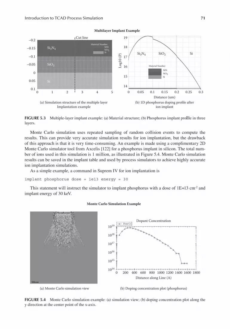
71Introduction to TCAD Process Simulation
Monte Carlo simulation uses repeated sampling of random collision events to compute the results. This can provide very accurate simulation results for ion implantation, but the drawback of this approach is that it is very time-consuming. An example is made using a complimentary 2D Monte Carlo simulator tool from Axcelis [122] for a phosphorus implant in silicon. The total num-ber of ions used in this simulation is 1 million, as illustrated in Figure 5.4. Monte Carlo simulation results can be saved in the implant table and used by process simulators to achieve highly accurate ion implantation simulations.
As a simple example, a command in Suprem IV for ion implantation is
implant phosphorus dose = 1e13 energy = 30
This statement will instruct the simulator to implant phosphorus with a dose of 1E+13 cm-2 and implant energy of 30 keV.
Multilayer Implant Example
Cut line 19–0.2
–0.15
–0.1
–0.05
0
0.05
0.10 1 2 3 4 5
18
17
16Log1
0 (P
)
15
140 0.05 0.1 0.15
Distance (um)(b) 1D phosphorus doping profile after
ion implant(a) Simulation structure of the multiple layer
Implantation example
0.2 0.25 0.3
Si3N4
SiO2
Si
SiNiMaterial Number
Material Number
SiO2Si
SiNiSiO2Si
Si3N4 SiO2 Si
FIGURE 5.3 Multiple-layer implant example: (a) Material structure; (b) Phosphorus implant profile in three layers.
Monte Carlo Simulation Example
Silicon
Phosphorous
(b) Doping concentration plot (phosphorus)
Distance along Line (A)
Dopant Concentration1019
1018
1017
1016
1015
1014
Dose C1
6004002000 800 1000 1200 1400 1600 1800
(a) Monte Carlo simulation view
FIGURE 5.4 Monte Carlo simulation example: (a) simulation view; (b) doping concentration plot along the y direction at the center point of the x-axis.

72 Integrated Power Devices and TCAD Simulation
5.4 DEPOSITION
In most process simulators, deposition is purely geometrical. The algorithm works by finding exposed surfaces and adding a new mesh layer on top of the existing mesh to mimic the physical progress of deposition. For flat surfaces, this task is easy, and the new layer just inherits the original x mesh while the y mesh is defined by user input. When a curvature exists, then two normal vectors (N1 and N2) are drawn from the original mesh line and projected for a given deposition thickness; a series of mesh points following the arc connecting the tips of N1 and N2 is then drawn to create a smooth deposit surface line [39]. Shown in Figure 5.5 is a deposition simulation example with curvature; here, a 2 µm thick oxide is deposited at a stepped silicon surface.
Please note that epitaxial growth in manufacturing is often simulated as a deposition; in situ doping of this deposited layer is also possible with Suprem IV. As a simple example, a command in Suprem IV for deposition is
deposit oxide thick = 0.01
This statement will deposit an oxide layer with a thickness of 0.01 µm.
5.5 OXIDATION
Oxidation is the process of converting silicon on the wafer surface into oxide. This chemical reaction already starts at room temperature, and the resulting very thin oxide film is called native oxide. The oxidation rate can be accelerated by exposing the wafer to oxygen or water vapor at high temperature. The growth of the thermally grown oxide depends on temperature, pressure, crystal orientation, doping
–2
–1
0
1
2
3
4
50 1 2
Material Number
N1 = N2 = 2 um
N2
N1
SiO2
Si
3 4 5
FIGURE 5.5 Illustration of deposition simulation with curvature.

73Introduction to TCAD Process Simulation
level, the impurity contamination of the silicon substrate, and stress due to nonplanar wafer structures [117] [123]. The grown oxide is commonly used as an insulator between single devices to act as a gate oxide in MOS structures and to serve as a mask against dopant implantation [117]. There are two tech-niques to get the silicon dioxide (SiO2) from pure silicon [116]: dry oxidation and wet oxidation.
5.5.1 dry oxidAtion
The silicon wafer is settled to a pure oxygen atmosphere at a temperature above 900°C. At the sur-face of the wafer a chemical reaction
+Si O SiO2 2 (5.3)
takes place. Because of a very low oxidation velocity (< 100 nm/h), this method is often used to generate high-quality thin oxide layers [117].
A simple command for dry oxidation is
diffuse time = 1 temp = 1000 dryo2
This statement will ask the simulator to grow a dry oxide at 1000°C for 1 minute.
5.5.2 wet oxidAtion
The silicon wafer is settled to a water vapor atmosphere and the reaction equation
+ +Si 2H O SiO 2H2 2 2 (5.4)
This process has a rather high oxidation velocity (>20 nm/min) and is therefore often used to get thick oxide layers for insulation and passivation techniques.
A simple command for wet oxidation is
diffuse time = 1 temp = 1000 weto2
This statement will ask the simulator to grow a wet oxide at 1000°C for 1 minute.
5.5.3 oxidAtion models
From a modeling point of view, process simulators provide both analytical and numerical models of the oxidation. Numerical models treat the oxide as a viscous incompressible fluid [124] [125] [126] [127] [128]; this involves solving the simplified Navier-Stokes equations inside the growing oxide [124] [125]. Interstitials injection phenomenon (a.k.a. oxidation enhanced phenomenon) from oxide to the bulk of silicon [129], [130], segregation of dopants (e.g., segregation of boron to oxide) phenomenon and stress effects are also included in the Suprem numerical models.
5.5.3.1 Moving BoundariesThe main problem encountered in the simulation of the oxidation is the movement of the oxide/silicon interface. This means that for each time step we solve the equations of the numerical model, regenerate the mesh, and then recalculate the interface boundaries. This requires an efficient mesh generator and efficient data management for this huge and frequently updated data [131]. From a numerical point of view, finite element discretization is preferred for oxidation simulation since the grid quality can be relaxed compared with the Voronnoi finite box technique. New process tech-nologies involve oxidation of nonrectangular structures [132] [117] so a three-dimensional oxidation simulator is needed to model arbitrary structures and include the three-dimensional effects [126].

74 Integrated Power Devices and TCAD Simulation
5.5.3.2 2D Analytical ModelsThe analytical models in the Suprem process simulator are based on the Deal Grove model [133] [134]. The basic idea of the model is the assumption of a steady state between three fluxes:
1. Oxidant’s flux (F1)
F1 is the flux of the oxidant (O2, H2O,…etc.) from the bulk of gas to the gas/oxide interface.
2. Diffusion flux (F2)
F2 is the diffusion flux across the oxide given by Fick’s law.
3. Reaction flux (F3)
F3 is the reaction flux corresponding to the oxidation reaction at the oxide/silicon interface.At steady state, these fluxes are identical and can be expressed as
= = =F F F F1 2 3 (5.5)
The flux of oxidant reaching the oxide/silicon interface is described in 1D by the differential equation developed by Deal Grove:
=N
dx
dtFox
1 (5.6)
where N1 is the number of oxidant molecules incorporated into a unit volume of oxide and (dxox)/dt represents the oxide growth rate. The solution to the 1D-oxide rate equation yields the final oxide thickness xox. It has been found that initially the oxide thickness (xox) versus time (t) curve is similar to linear growth rate, which then becomes parobolic. This is seen in Figure 5.6, which is a typical representation of oxide growth [135].
The analytical models can be used only for simple planar structures. Most of the time, numerical models are used in TCAD simulation.
5.5.3.3 Numerical ModelsFrom a mathematical point of view, the numerical oxidation models can be described by a cou-pled system of partial differential equations. The diffusion equation describes the diffusion of the
Oxide Growth vs. Time
Parabolic
Time
Oxi
de
ickn
ess Linear
FIGURE 5.6 Oxide growth curve.

75Introduction to TCAD Process Simulation
oxidant in the existing silicon dioxide. The chemical reaction equations describe the transformation of silicon to silicon dioxide. Finally, the displacement equations are about the displacement and expansion of the oxide layer and neighboring materials.
At high temperatures, the oxide layer is modeled as an elastic [126], viscoelastic [136] [137] [126] [128], or viscous compressible or incompressible flow [124] [125] [126] [127] [128]. Due to unknown motion of the interface between silicon and silicon dioxide this leads to a free boundary problem [126] [127] [128].
Three numerical models are provided by Suprem: vertical, compress, and viscous. The vertical model indicates that the oxidant should be solved for and that the growth is entirely vertical. The compress model treats the oxide as a compressible liquid. The viscous model treats the oxide as an incompressible viscous liquid. Real oxide is believed to be incompressible; however, the compress-ible model is a lot faster, so there is a trade-off between accuracy and speed [116]. These models are compared in Table 5.2.
5.5.3.4 LOCOS Growth ExampleLocal oxidation of silicon (LOCOS) is a typical process step in power integrated circuits. Here a simulation example is given so that readers can get familiar with the oxidation simulation. First an oxide layer of about 40 nm is thermally grown and followed by a deposition of silicon nitride (Si3N4) of about 80 nm thick as an oxidation mask. Silicon nitride is then selectively etched, leaving a win-dow for LOCOS growth. A wet oxide thermal process at 1000°C for 90 minutes is subsequently car-ried out and the nitride is etched away at the end, leaving the bird’s beak-shaped LOCOS. Interested readers can refer to [135] for more detailed process steps of LOCOS growth. Figure 5.7 illustrates the LOCOS growth simulation with enlarged view of the “bird’s beak” after wet oxidation (before nitride is removed).
5.6 ETCHING
Like deposition, etching in the process simulation is purely geometrical, and no chemical reaction is included. This is relatively easy if the required etching shape simply has straight edges, be they purely vertical or at an angle. However, if an arbitrary shape is required, we need to specify some parameters for the Suprem process simulator.
Reactive ion etching (RIE) is a mainstream etching method in modern IC technologies: put simply, the unmasked silicon surface is subjected to high-energy ion bombardment that knocks out the mate-rial being exposed [39]. Ideally, no side wall should be created by RIE, but in reality there is always a sidewall effect due to the isotropic etching rate. In this case, using a geometrical etching method is sometimes necessary; the etching rate (µm/s) and etching time (s) in both the vertical and horizontal directions must be provided. Figure 5.8 is an example of geometrical etching creating a curved surface.
A simple example of etching command is something like this:
etch silicon thick = 0.2 dry
This will ask the simulator to perform a dry etching of silicon with an etching depth of 0.2 µm.
TABLE 5.2Comparison of Numerical Models for Oxidation
Models Planar or Nonplanar Stress Effect Accuracy Speed
Vertical Only for Planar No stress effect Low Fast
Compress Planar and Nonplanar No stress effect Medium Medium
Viscous Planar and Nonplanar With stress effect High Slow

76 Integrated Power Devices and TCAD Simulation
0
0.2
0.4
0.6
0.8
10 0.5 1
Material NumberSi
1.5 2 2.5
FIGURE 5.8 A geometrical etching example.
LOCOS Growth Example0
1
2
3
4
5
0
1
2
3
4
5
0
1
2
3
4
50 1 2 3 4
(c) After LOCOS growth (d) After LOCOS growth-enlarged view
(a) Oxide growth and nitride deposition (b) Nitride etch
5 6 7 8 9 10
0 1 2 3 4 5 6 7 8 9 10 0 1 2 3 4 5 6 7 8 9 10
2 2.5 3 3.5
–0.3–0.2–0.1
00.10.20.30.40.5
Material NumberSiNiSiO2Si Material Number
SiNiSiO2Si
Material NumberSiNiSiO2Si
Material NumberSiNiSiO2Si
FIGURE 5.7 LOCOS growth example.

77Introduction to TCAD Process Simulation
5.7 DIFFUSION
Diffusion is one of the main challenges in designing a process flow, since the placement of the active doping regions need to be accurately controlled. Proper selection of diffusion conditions is crucial for obtaining desired device electrical characteristics [135].
In terms of process simulation, diffusion is by far the most time-consuming step if the number of nodes is large. The latest models of impurity diffusion are often based on the concept of pair diffu-sion. These models account for interactions not only between impurities and space charge but also between impurities and lattice point defects such as interstitials and vacancies [39]. Impurity atoms cannot diffuse on their own and need neighboring point defects as diffusion vehicles so it is com-mon to denote a diffusing dopant involved in a diffusion mechanism as a dopant–defect pair. When the binding energy between an impurity and a neighboring defect is not too weak, the impurity and the the point defect will move as a dopant–defect pair until they get separated by recombination or other effects. Two types of defects exist: vacancies and interstitials. Thus, we label a dopant A paired with a vacancy V as an AV pair and a dopant A paired with an interstitial I as an AI pair. Diffusivities of dopants always represent the diffusivities of the dopant–defect pairs.
The recombination between the paired dopants and other species (as unpaired defects) is not included in the equations in Suprem. The chemical reaction rate equations of these types of recombi-nation are AV+I ⇔ A in case of the Frank–Turnbull recombination and AI+V ⇔ A in case of a dissolu-tion process [117].
5.7.1 diFFusion mecHAnisms
Suprem includes three basic diffusion mechanisms for dopant diffusion models [138] [139] [140] [117].
5.7.1.1 Direct Diffusion MechanismIn direct diffusion, impurities with small ionic radii can travel directly from one interstitial site to another. Group I and Group III elements in particular tend to diffuse directly and are therefore fast diffusers.
5.7.1.2 Vacancy MechanismIn this diffusion mechanism, a substitutional dopant exchanges its position with an adjacent or neighboring vacancy. The vacancy should move at least to a third neighbor site away from the dop-ant to prevent oscillations. For more details about this regime, see [139].
5.7.1.3 Interstitials MechanismThis mechanism is also called a kick-out mechanism. In the case of silicon, the dopant at a substi-tutional site is approached by a silicon interstitial and kicked out to reside at an interstitial position while the original self-interstitial has disappeared by occupying the regular lattice site. This inter-stitial dopant can now move toward an adjacent lattice site to regenerate a self-silicon interstitial by the same kick-out mechanism.
The most commonly used P-type dopant (boron) tends to diffuse via interstitials. The N-type dopant phosphorus tends to diffuse via interstitials at low doping and via a dual mechanism at high doping concentrations, with a strong bias toward vacancy diffusion. Arsenic also uses interstitials and vacancies for its diffusion. However, its interstitial mechanism is limited due to the relatively large ionic radii [117], and large impurities such as antimony diffuse only via vacancies. The rate equations for the basic atomistic diffusion mechanisms are
A+V ⇔ AV (5.7)
A+I ⇔ AI (5.8)
Unlike impurities, point defects can travel on their own, so their diffusion models are based on two concepts: paired and unpaired diffusion. Paired diffusion is already implicitly included in the impurity diffusion models, so an extra equation only for the unpaired defect diffusion needs to be

78 Integrated Power Devices and TCAD Simulation
added as the diffusivity of paired and unpaired point defects can be very different. The diffusion of defects is also limited or stopped by the recombination effects. The recombination reaction between interstitials and vacancies is also included in the Suprem models. Table 5.3 lists the chemical reac-tions of pair diffusion models with interstitials (I) and vacancies (V).
A simple command for diffusion works like this:
diffuse time = 1 temperature = 1050 nitrogen
This will allow the simulator to perform a diffusion process simulation at a furnace temperature of 1050°C for 1 minute within the nitrogen enviroment.
5.7.2 diFFusion models
There are four different diffusion models in Suprem. The accuracy of each model depends mainly on how the point defects are modeled and simulated.
5.7.2.1 Fermi Diffusion ModelThis model is the fastest in CPU time. In this simple model, the free point defects equations are not solved since they are assumed to be in thermodynamic equilibrium. In this model, only the equations repre-senting the diffusion of dopant–defect pairs are solved, and their diffusivity coefficients are supposed to be time-independent. This model therefore cannot be used to simulate transient-enhanced, oxidation-enhanced, or retarded diffusion in which the free point defects are not in thermodynamic equilibrium.
5.7.2.2 Two-Dimensional Diffusion ModelIn this model, the free point defects can evolve over time, and the equations representing their dif-fusion are solved. The diffusivity coefficients of the dopant–defects pair diffusion equations are enhanced to include the transient effects of the free point defects so the diffusion of the dopants is strongly affected by the diffusion of the free point defects. In this model, the diffusion of free point defects is not affected by the diffusion of dopants: mathematically speaking, the diffusion equa-tions of free point defects are decoupled from the diffusion equations of dopants, and there is only one-way coupling between impurities and defects. This model can be used to include the oxidation-enhanced or retarded-diffusion effects and costs more CPU time than the Fermi model.
5.7.2.3 Fully Coupled Diffusion ModelIn this model, the diffusion of the free point defects is affected by the diffusion of the dopants. This coupling adds the dopant–defect pair diffusion fluxes to the diffusion fluxes of the free point defects. This model is an extension of the two-dimensional model, which in turn is an extension of the Fermi model. The fully coupled model is physically more accurate, and it was used in different process simulations to predict different physical effects observed in the processing. However, even this model still suffers from not being able to take into account the explicitly paired and unpaired dopants point defects diffusion.
TABLE 5.3Chemical Reactions of Pair Diffusion Models with Interstitials (I) and Vacancies (V)
Silicon Boron Phosphorus Arsenic Antimony
I+V ⇔ 0 B+I ⇔ BI P+I ⇔ PI As+I ⇔ AsI Sb+V ⇔ SbV
BI+V ⇔ B P+V ⇔ PV As+V ⇔ AsV SbV+I ⇔ Sb
PI+V ⇔ P AsI+V ⇔ As
PV+I ⇔ P AsV+I ⇔ As

79Introduction to TCAD Process Simulation
5.7.2.4 Steady-State Diffusion ModelThis model is a special case of the two-dimensional model in which the point defects are assumed to be at steady state.
5.7.2.5 Oxide Enhanced (Retarded) DiffusionIt has been found that some dopants appear to have their diffusion coefficients enhanced or reduced when the surface of the silicon is oxidized. When oxide grows, there is a 30% expan-sion that occurs to form the SiO2 structure and interstitials are injected to relieve the com-pressive stress. Impurities such as boron and phosphorus have a tendency to diffuse through interstitials so an enhanced diffusion rate is observed. On the contrary, antimony seems to diffuse with vacancies. Since the injected interstitials reduces the population of vacancies in the silicon bulk (through recombination [135]), the diffusion of antimony is retarded during oxidation. Table 5.4 shows the oxide-enhanced (or retarded) diffusion of several impurities.
Figure 5.9 is a simulation result of buried n+ (phosphorus implant) layer diffusion with oxidation. We see a noticeable diffusion enhancement of phosphorus at the location where oxidation took place.
TABLE 5.4Oxide Enhanced (or Retarded) Diffusion of Several Impurities
Boron (B) Phosphorus (P) Arsenic Antimony (Sb)
Oxide-enhanced diffusion X X X
Oxide-retarded diffusion X
Oxide Enhanced Diusion Example
Oxide
Silicon
Material Number
Net_Doping201510
50–5–10–15
Net_Doping17.1081510
50–5–10–15–15.0005
(Pa/Ba/) Signed _Log1017.108151050
–5–10–15–15.0005
SiNi
SiSiO2
–2
–1
0
1
2
3
(b) Oxide growth after oxidation0 1 2 3 4 5 6 7 8 9 10
Silicon
Implanted dopants–2
–1
0
1
2
3
(a) Net doping before oxidation0 1 2 3 4 5 6 7 8 9 10
–2
–1
0
1
2
3
(b) Net doping after oxidation showing oxideenhanced diusion at LOCOS region
0 1 2 3 4 5 6 7 8 9 10
–2.5
–2
–1.5
–1
(d) Enlarged view to show oxide enhanceddiusion
1.5 2 2.5 3 3.5 4 4.5
FIGURE 5.9 Simulation results of oxide enhanced diffusion of phosphorus.

80 Integrated Power Devices and TCAD Simulation
5.8 SEGREGATION
A problem device design engineers often faced with is dopant segregation at the interface between oxide and silicon. Segregation is defined here as the preference of dopants to reside in either oxide or silicon. Different dopants have very different segregation tendencies: boron tends to stay in the oxide, which depletes the silicon surface; arsenic and phosphorus prefer staying in the silicon, which result in a pile up at the oxide/silicon surface [121].
To clarify the segregation effect, a simulation example starts with silicon substrate with an initial phosphorus concentration of 1E+17 cm–3. A dry oxidation step is then done at a temperature of 1000°C for 300 minutes, which yields an oxide thickness of about 800 Å. From Figure 5.10 we see that the phosphorus dopants are piled at the silicon surface, while the doping level in the oxide is much lower.
A comparison is made with a boron-doped substrate with a doping concentration of 1E+17 cm–3. After dry oxidation (temperature of 1000°C and 300 minutes), the boron is depleted in the silicon surface while piling up in the oxide, as shown in Figure 5.11.
In Suprem, segregation can be tuned by modifying the segregation coefficients. The segregation model is calculated using [116]:
⋅ = −
J n T CC
Mseg r 1
2
12 (5.9)
where ⋅J nseg is the normal flux of dopants flowing from material 1 to material 2 across the inter-
face. C1 and C2 are the concentrations in materials 1 and 2, respectively. Tr is the transport velocity, which takes into account the rate of dopants crossing the interface. M12 is the segregation term tak-ing into account the variation of the threshold solubility of dopants in the two neighboring materials [39]. For each diffusing dopant A, we have
=M
TS A
TS A
( )( )
121
2 (5.10)
0
0.5
1
1.5
20 1 2 3 4 5 6 7 8 9 10
15.0599
15.5
16
16.5
17
17.0732
(Pa/)Signed_Log10
Cut lineSiliconPhosphorus Piles Up
Oxide
Oxide Silicon
Material NumberSiO2Si
0.30.250.20.15Distance (um)
0.10.05015.215.415.615.8
16
Net
_Dop
ing
16.216.416.616.8
17
FIGURE 5.10 Phosphorus segregation example.

81Introduction to TCAD Process Simulation
where TS1(A) is the threshold solubility of the dopant A in material 1. TS2(A) is the threshold solu-bility of the dopant A in material 2, while M12 and Tr are calculated using a standard Arrhenius relationship. The process simulator allows the user to set these parameters using the impurity name as a command with parameters such as Seg.0, Seg.E, Trn.0, and Trn.E. The meanings of these parameters are listed in Table 5.5 [39].
The Suprem default segregation coefficient parameters for various dopants (at (100) orientation) are listed in Table 5.6. Note that these segregation coefficients are for silicon/oxide interface only.
0
0.5
1
1.5
20 1 2 3 4 5 6 7 8 9 10
–16.2
–16.4
–16.6
–16.8
–17
–17.2
–16Cutline
Silicon
Oxide
Oxide Silicon
Boron Piles Up
Net_Doping
Material NumberSiO2Si
0.30.250.20.15Distance (um)
0.10.050
16.216.316.416.516.6
Net
_Dop
ing
16.716.816.9
1717.1
FIGURE 5.11 Boron segregation example.
TABLE 5.5The Segregation Coefficients Parameters and Meanings
Parameters Meaning
Seg.0 Pre-exponential constant for segregation
Seg.E Activation energy for segregation
Trn.0 Pre-exponential constant for transport
Trn.E Activation energy for transport
TABLE 5.6The Suprem Default Segregation Coefficient Parameters for Various Dopants
Dopants Seg.0 Seg.E Trn.0 Trn.0
Boron 1126 0.91 1.66e-7 0
Phosphorus 30 0 1.66e-7 0
Arsenic 30 0 1.66e-7 0
Antimony 30 0 1.66e-7 0

82 Integrated Power Devices and TCAD Simulation
5.9 PROCESS SIMULATOR MODELS CALIBRATION
As mentioned earlier, TCAD plays an indispensable role in the technology development of semi-conductor devices and ICs. TCAD enables the experimental results to be simulated and analyzed before running any experimental lots; the results obtained can be used to improve the DoE (design of experiment) analysis and reduce the number of development lot, which reduces the total develop-ment time and cost [141] [142]. However, the accuracy of TCAD simulation depends on how well the process and device simulators are calibrated with experimental data obtained using a particular set of equipment and fabrication facilities. For example, if the simulators are not calibrated and are used with default model parameters only, an unacceptable discrepancy between the simulated results and experimental data might be obtained. In this section, a general approach to calibrate the models for a process simulator will be discussed, and models calibration for a device simulator will be given in the next chapter.
A process simulator has to be calibrated such that physical properties of the simulated device, especially the doping profiles and film thickness, can be as close as possible to those of the experi-mental device [143]. The doping profiles are mainly determined by ion implantation and thermal dif-fusion processes. The thickness of the different films for building the device is mainly determined by oxidation, deposition, and etching processes, whereas the oxidation process is the most critical one due to the associated relatively high thermal budget. Models calibration starts with running shoot-loop experiments with various process conditions. For examples, in addition to the species of impurities, dose and energy are varied in those shoot-loop experiments for the ion implantation, and temperature and duration are varied in those shoot-loop experiments for the thermal diffusion and oxidation processes. The range of the process conditions of the short-loop experiments should at least cover the range of the process conditions of the desired process flow. The number of short-loop experiments needed depends on the required accuracy of the calibration. It can be over 20 [144] or even over 100 [145] for very accurate calibration. The experimental doping profiles can be extracted by using secondary ion mass spectroscopy (SIMS) or spreading resistance profiling (SRP), and the film thickness can be extracted by using scanning electron microscope (SEM) or transmission elec-tron microscope (TEM). The experimental data are compared with the simulated results generated by the process simulator. If the discrepancy between the simulated results and experimental data is unacceptable, the default models and model parameters used in the simulator have to be adjusted until the discrepancy becomes acceptable.
Calibration of a popular process simulator, TSUPREM-4 [146], is given in the following section as an example for illustration. The default analytical model for the ion implantation process is the Pearson distribution. Four model parameters (range, standard deviation, skewness, and kurtosis) with respect to different impurities, dose, and energy of the implantation can be adjusted to calibrate the simulated doping profiles with the experimental ones extracted by SIMS or SRP. The damages to silicon (e.g., point defects) produced during the implantation, which are critical to transient-enhanced diffusion (TED), can also be modeled in the process simulator. Furthermore, the dif-fusivities of the various impurities in the process simulator can be adjusted for the doping profiles calibration. Modeling of thermal diffusion of point defects and segregation of impurities at material interfaces is also allowed for a more precise calibration of doping profiles. Moreover, the oxidation rate in the process simulator can be adjusted so that the simulated oxide thickness matches the experimental oxide thickness extracted by SEM or TEM.
5.10 INTRODUCTION TO 3D TCAD PROCESS SIMULATION
With ever more complicated structures, three-dimensional effects are getting a lot of attention from power semiconductor device designers. 3D TCAD simulation is becoming more and more important, since a successful 3D simulation can lead to better understanding of 3D effects in modern device designs. In the past, 3D TCAD was very difficult to realize because of constraints on computing

83Introduction to TCAD Process Simulation
power. With the dramatic improvement of CPU speed and multicore architecture, 3D simulation is becoming a daily practice for device designers.
3D TCAD mesh generation can be done in two different ways. The traditional method used in mechanical and fluid simulations relies on pyramid-like mesh elements and is popular because of relatively mature mesh generation algorithms. However, it comes at the price of huge total mesh count when mesh density changes rapidly.
Another method uses stacked planes with prism-shaped mesh elements; this results in less over-all mesh and much better convergence. One main advantage of plane stacking is that an optimized 2D mesh can be directly imported to a 3D simulation. Interested readers can refer to [39] for more information. Figure 5.12a is a 3D TCAD process simulation of a diode, with anode (circle) on top and cathode at the bottom. Figure 5.12b is a simulation mesh structure of vertical DMOS with multiple hexagonal-shaped poly gates [147] [148].
A three-dimensional circular shaped LOCOS oxidation is shown in Figure 5.13. The finished 3D LOCOS with a nitride layer removed looks like a “saucer.” The process parameters are the same
Some 3D Process Simulation Examples
(a) Power diodes with anode on top (circles) andcathode at the bottom
(b) Hexagonal shaped gates of a verticalDMOS
Material Number
Net_Doping19
15
10
5
0
–5
–10
–15
–19.6449 224
68
101214
16+x
00
1.5
1
0.5
0
–Y+Z
1614
12
86
42
10
PolySi
24
68
10+x
00
–0.5
–0
–1
–1.5
–2
–Y
+Z
8
4
6
2
10
FIGURE 5.12 Some 3D TCAD process simulation examples.
Some 3 D Process Simulation Examples
(a) Oxide and nitride mask before oxidation (b) After oxidation with silicon and nitrideremoved
–Y
–Z
–Z
43.5
32.5
21.5
10.5
Material NumberSiNiSiO2Si
Material NumberSiNiSiO2Si
000.51
1.52
2.53
3.54
0 00.5 0.51 11.5 1.52 22.5 2.53 33.5 3.54 10.8
0.6
0.4
0.2
–Y
4+X +X
00.20.40.60.81
FIGURE 5.13 3D oxidation of a circular-shaped LOCOS.

84 Integrated Power Devices and TCAD Simulation
as the 2D LOCOS simulation shown in Figure 5.7, except a 3D process simulation method called “bent planes” is applied. For more information about bent planes, please refer to [39].
5.11 GPU SIMULATION
The computational requirements for the 3D process and device simulations are very cumbersome due to the large mesh size and memory requirements. Depending on the complexity and computer configuration, a complicated 3D simulation can takes days or even weeks. In recent years, parallel processing such as the CUDA platform from NVidia is becoming more and more popular among scientists and engineers. CUDA enables dramatic increases in computing performance by harness-ing the power of the graphics processing unit (GPU) [149].
Modern computers primarily divide the tasks they are assigned to do between two different processing units: the CPU, which is the “brain” of the computer and handles all general-purpose tasks; and the GPU, which handles specialized instructions related to the video display. As shown in Figure 5.14a, a simplified architecture view shows the CPU has a control unit and one or more arith-metic logic units (ALUs), which extract instructions from memory, decode, and then execute them [150]. The GPU, on the other hand, is designed to rapidly manipulate and alter memory to accelerate the creation of images in a video display’s output buffer [151]. The GPU is thus designed in a very different way from the CPU: as illustrated in Figure 5.14b, the number of processing cores is greatly increased, which gives it the ability to run a large number of highly specialized jobs in parallel.
This means that the GPU excels at tasks that can be well parallelized such as 3D shaders, which can accommodate the display of millions of pixels in a video game. The trade-off is that the individ-ual cores are slower than those of a CPU, so the GPU fares poorly on tasks that cannot easily be done in parallel. This limitation in the speed gains due to parallelism is known as Amdahl’s law [153].
The key to a successful GPU-accelerated simulation is thus to separate the tasks in the program that need to be done in a serial manner from those than can be run in parallel. The serial portions of the code run on the high-speed CPU, while parallel portions run on the GPU [154]. For 3D device simulation, the most time-consuming part of the code is the sparse matrix linear solver at the heart of the nonlinear Newton method, so specialized algorithms that maximize parallelism are needed.
In the case of a 3D process simulation, the most time-consuming aspect of the simulation is the 3D diffusion. Benchmark tests have been carried out to determine how the GPU + CPU simulation
(a) Simplied architecture representationof a CPU
(b) Simplied architecture representationof a GPU
DRAMDRAM
Cache
Simplied Architecture Representation of a CPU and GPU
ControlALU
ALU
ALU
ALU
FIGURE 5.14 Simplified architecture comparison between a CPU and a GPU [152].
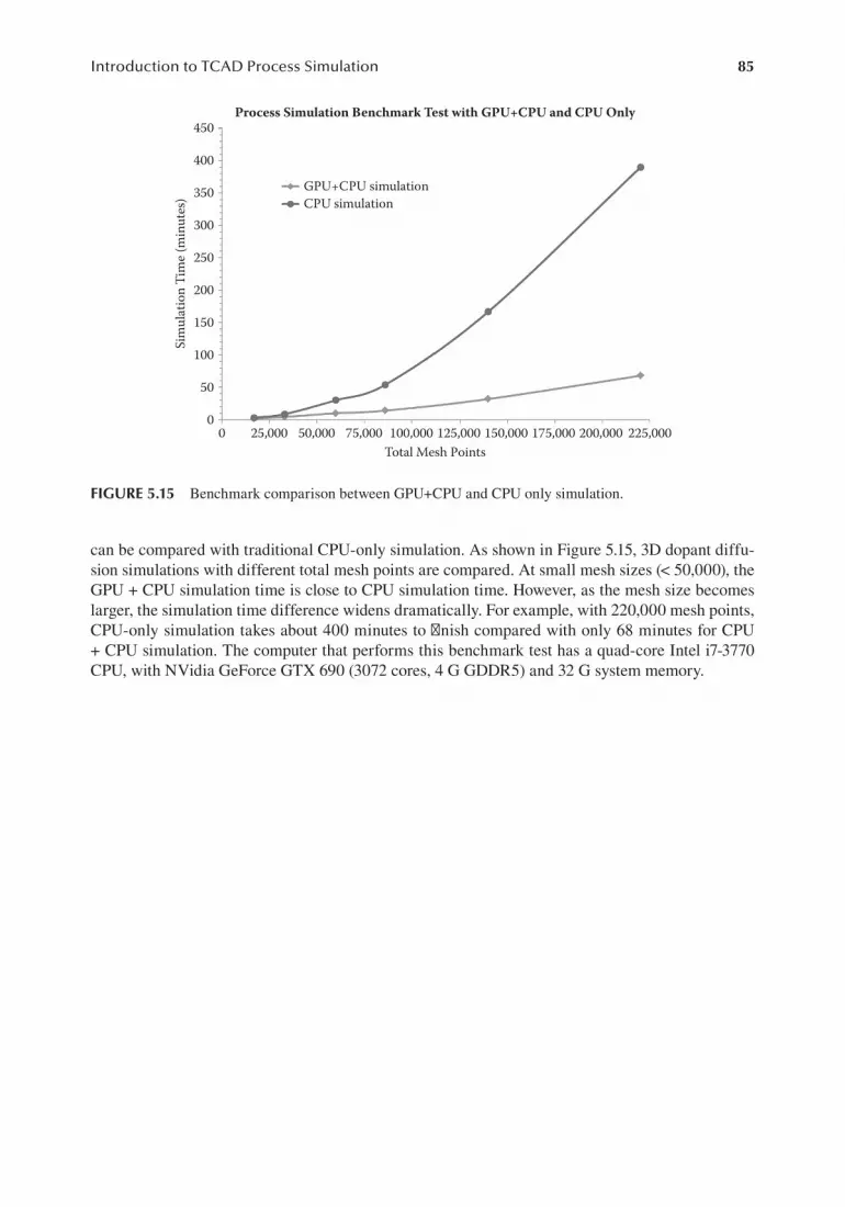
85Introduction to TCAD Process Simulation
can be compared with traditional CPU-only simulation. As shown in Figure 5.15, 3D dopant diffu-sion simulations with different total mesh points are compared. At small mesh sizes (< 50,000), the GPU + CPU simulation time is close to CPU simulation time. However, as the mesh size becomes larger, the simulation time difference widens dramatically. For example, with 220,000 mesh points, CPU-only simulation takes about 400 minutes to finish compared with only 68 minutes for CPU + CPU simulation. The computer that performs this benchmark test has a quad-core Intel i7-3770 CPU, with NVidia GeForce GTX 690 (3072 cores, 4 G GDDR5) and 32 G system memory.
Process Simulation Benchmark Test with GPU+CPU and CPU Only
GPU+CPU simulation
450
400
350
300
250
Sim
ulat
ion
Tim
e (m
inut
es)
200
150
100
50
00 25,000 50,000 75,000 100,000
Total Mesh Points125,000 150,000 175,000 200,000 225,000
CPU simulation
FIGURE 5.15 Benchmark comparison between GPU+CPU and CPU only simulation.


87
6 Introduction to TCAD Device Simulation
Chapter 5 introduced the TCAD process simulation. This chapter focuses on TCAD device simulation.
6.1 OVERVIEW
Device simulation investigates the electrical, thermal, and optical properties of semiconductor devices. This section highlights some of the most important aspects for power device simulation, such as impact ionization and mobility. Experienced readers should refer to [39] for a more advanced treatment of simulation equations and explanations. Figure 6.1 shows a simplified flow of TCAD device simulation.
6.2 BASICS ABOUT DEVICE SIMULATION
6.2.1 driFt-diFFusion model
The basic semiconductor model is the drift-diffusion model. Even with more advanced models now available, drift-diffusion remains the workhorse of the industry since it can be used to explain many of their important characteristics such as the ability to amplify electrical signals. The most important parts of drift-diffusion theory are the Poisson and current continuity equations. Two optional equa-tions (hydrodynamic model) are sometimes used to describe the carrier energy/temperature distribu-tion; this should not be confused with the lattice temperature, as these equations describe how the carrier distribution deviates from the Fermi–Dirac distribution. For each mesh point, these equations are solved self-consistently for the electrostatic potential, the electron (hole) concentrations and the electron (hole) energies. The basic relationship between these equations is shown in Figure 6.2.
These differential equations are discretized as described in the next section. The resulting set of equations is coupled nonlinearly, and consequently no method exists to solve these equations in one direct step. Instead, solutions must be obtained by a nonlinear iteration method, starting from some initial guess.
6.2.2 discretizAtion
To solve the device equations on a computer, they must be discretized on a simulation grid. That is, the continuous functions of the partial differential equations (PDE) are represented by vectors of function values at the nodes and the differential operators are replaced by suitable difference opera-tors. This means that the simulator solves for 3N unknowns (potential and electron–hole concentra-tions), where N is the number of grid points; additional variables for the electron–hole energy are used if the hydrodynamic model is turned on.
The key to discretizing the differential operators on a general triangular grid is the box method [155]. Each equation is integrated over a small polygon enclosing each node, yielding 3N nonlinear algebraic equations for the unknown potential and carrier concentrations. The integration equates the flux into the polygon with the sources and sinks inside it so that conservation of current and electric flux is built into the solution. Compared with the finite element method, which performs

88 Integrated Power Devices and TCAD Simulation
integrals on a triangle-by-triangle basis, the box method produces an elegant method of handling general surfaces and boundary conditions: the integral is simply replaced by a summation of the integrand evaluated at the mesh node, multiplied by its surrounding area.
6.2.3 newton’s metHod
In this section, we will discuss the numerical solution of drift-diffusion equations. In Newton’s method, all of the coupling between variables is taken into account, and these variables are allowed
Export for Plotting
Scan Potential or Currentat Certain Contacts
Equilibrium(set all contacts’ potential to 0)
Newton Iteration Parameters Define
Physical Models(impact ionization, mobility models, etc.)
Materials and Contacts Define
Data Import fromProcess Simulator
Drawn from Scratch(w/o process simulator)or
FIGURE 6.1 A simplified flow of TCAD device simulation.
Electron & HoleEnergies
Electron & HoleConcentrationsElectrostatic Potential
ese Equations Are SolvedSelf-Consistently
for:
Drift-Diffusioneory
Poisson Equation
Current Continuity Equations
Hydrodynamic Model
Governs the ElectrostaticPotential
Governs the CarrierConcentrations
Describes the CarrierEnergy or TemperatureDistribution
FIGURE 6.2 Drift-diffusion theory.

89Introduction to TCAD Device Simulation
to change at every iteration. Due to this, the Newton algorithm is very stable, and the solution time is nearly independent of bias conditions. The basic algorithm is a generalization of the Newton-Raphson method used to find the root of a single equation. The Poisson equation and current conti-nuity equations can be written as
, , 01 1 1( ) =F V E Ev
j jfnj
fpj (6.1)
, , 01 1 1( ) =F V E En
j jfnj
fpj (6.2)
, , 01 1 1( ) =F V E Ep
j jfnj
fpj (6.3)
where j runs from 1 to N, and j1 includes j itself plus its surrounding mesh points. These equa-tions represent a total number of 3N equations, which are sufficient to solve for 3N variables:
…( )V E E V E E V E Efn fp fn fpN
fnN
fpN, , , , , , , , .1 1 1 2 2 2
Once the equations are discretized in the previous form, standard Newton techniques can be used to solve for them. These involve evaluating the Jacobian matrix to linearize the equations, followed by a linear solver (involving lower and upper triangular matrix [LU] factorization of the matrix), and finally nonlinear iterations to get the final solution. Since the Jacobian matrix is sparse, sparse matrix techniques are used to improve the computation speed.
A major speed-up of Newton iterations is accomplished with the Newton–Richardson method, whereby the Jacobian matrix is refactored only when necessary. When it is not necessary to fac-torize, the iterative method using the previous factorization is employed. The iterative method is extremely fast provided the previous factorization is reasonable. Frequently, the Jacobian needs to be factorized only once or twice per bias point using the Newton–Richardson method, as opposed to the 20 to 30 times required in the conventional Newton method. The decision to refactor is made on the basis of the rate of decrease of the maximum error of the equation residuals and variable dif-ferences per nonlinear iteration. This mechanism has been automated within most simulators and no user intervention is needed [156].
6.2.4 initiAl guess And AdAptive BiAs stepping
Several types of initial guess solutions are used in the TCAD simulator. The first is the simple charge neutral assumption used to obtain the first (equilibrium) bias point. This is the starting point of any device simulation.
Any later solution with applied bias needs an initial guess of some type, obtained by modifying one or more previous solutions. When only one previous solution is available, the solution currently loaded is used as the initial guess, modified by setting the applied bias at the contact points. When two previous solutions with two different biases are available, it is possible to obtain a better initial guess by extrapolating the two previous solutions.
All of these steps are automated within the program. A schematic of the biasing strategy is given in Figure 6.3.
As in any Newton method, convergence strongly depends on the choice of the initial guess solution. In principle, the Newton nonlinear iteration should always converge as long as the initial guess is close enough to the solution; the closer the initial guess is to the solution, the fewer non-linear iterations are required to reach convergence. The program takes this fact into account and implements an adaptive method to control the bias step after the successful convergence of the previous solution.
Assuming that the previous solution takes K1 number of iterations for a bias step of ΔV1 to reach convergence and the user believes (by experience) that the optimal number of iterations

90 Integrated Power Devices and TCAD Simulation
should be K0, the current bias step ΔV2 is adjusted to /2 1 0 1=V V K K . In this way an optimal step can be determined such that the nonlinear Newton iteration is controlled to converge within K0 iterations.
One common cause of convergence problems in a Newton method is oscillations in the solution. This usually occurs when the initial guess is poor and the solver overshoots the solution. To prevent this, a damping value can be implemented, which prevents the solver to change the solution too much between successive iterations. A small damping value will damp the oscillations effectively but may cause slower convergence. A large value allows faster convergence when the initial guess is poor but carries a larger risk of oscillations.
6.2.5 convergence issues
Quite often, convergence issues plague TCAD users. The choice of voltage or current bias affects the convergence and stability of the Newton solver. To guarantee convergence, small changes in the applied bias should always result in small changes in the overall solution.
One particular situation where current bias is not appropriate is when the total amount of current flowing in the device is very small. Under these conditions, the actual current amount may fluctu-ate due to lack of numerical precision, making it difficult to use current bias. This situation can be detected by observing the net current over all the electrodes: if the sum is not zero, then Kirchhoff’s current law is violated, and the current is too low to use as a control variable.
If we take a forward-biased diode as an example, the solver can enter a nonconvergent state if the applied (anode) voltage bias is much higher than the turn-on voltage. Since the conductivity increases exponentially with bias in a typical diode, seemingly small changes in voltage can result in very large changes of the solution.
This leads us to a simple general rule:
1. Use voltage bias for devices with high resistance. 2. Use current bias for devices with low resistance.
All solversconvergent and
consistent?
Yes
No
Adjustment of bias
Frequently updated waveequation solver
Fully coupled solution ofsemiconductor drift-diffusion
equations plus photon rate equation
A new current/voltage bias
FIGURE 6.3 Flow diagram of how the simulator performs in a typical device simulation.

91Introduction to TCAD Device Simulation
For example, a typical diode under forward bias has low resistance past its turn-on point but high resistance at lower bias or under reverse bias conditions. With these two extremes in mind, the following general strategy is recommended when setting up a simulation under forward bias:
1. Solve for equilibrium solution. 2. Apply voltage until 80–90% of the built-in bias value is reached. Some software tools also
allow the possibility of terminating the voltage increase once certain current conditions have been met.
3. Verify that Kirchhoff’s current law is satisfied at this bias point. 4. Apply current bias until desired value is reached.
6.2.6 BoundAry conditions
The boundary conditions for the electrical part include Ohmic contacts, Schottky contacts, Neumann (reflective) boundaries, lumped elements, and current controlled contacts. For the hot carrier equa-tions, the boundary condition is the contact carrier temperature.
6.2.6.1 Ohmic ContactOhmic contacts are implemented as simple Dirichlet boundary conditions where the surface poten-tial and electron and hole quasi-Fermi levels Vs E Efn
sfns( , , ), are fixed.
The minority and majority carrier quasi-Fermi potentials are equal and set to the applied bias of the electrode:
φ = φ = − = − =E E Vns
ns
fns
fps
applied (6.4)
The potential Vs at the boundary is fixed at a value consistent with zero space charge. With the solution of Vs and Equation (6.4), ns and ps can be calculated.
It should be pointed out that the purpose of creating an Ohmic contact in a simulation is to have a boundary condition that does not disturb the area of simulation but provides a path for current flow. This is in contrast to the Schottky contact that can be either injecting or depleting carriers, depend-ing on the polarity of the bias.
In most device simulations, the ideal Ohmic contact with a charge neutral assumption is sufficient as a good carrier injector if the contact area is highly doped or if the carrier injection requirement is not too high. If the vicinity of the contact has low doping or if a high level of carrier injection is required, the ideal Ohmic boundary described above ceases to be a valid model for a realistic Ohmic metal contact.
6.2.6.2 Schottky ContactsSchottky contacts to the semiconductor are defined by the barrier height of the electrode metal and a surface recombination velocity. The surface potential at a Schottky contact is defined by
= χ − χ φ +V Vs ref b applied– (6.5)
where χ and χref are the electron affinities of the semiconductor and a reference material, respec-tively, and ϕb is the Schottky barrier height.
Note that this applies only for n-contacts. For p-contacts, this equation needs to be modified by the semiconductor bandgap to calculate the proper hole barrier. The sum of the barrier heights for electrons and holes is expected to be equal to the bandgap [138].

92 Integrated Power Devices and TCAD Simulation
In general, the quasi-Fermi levels E fns and E fp
s are no longer equal to Vapplied and are defined by a current boundary condition at the surface instead:
( )= γ −J v n nsn n nthm
s eq (6.6)
( )= γ −J v p psp p pthm
s eq (6.7)
where Jsn and Jsp are the electron and hole currents at the contact, ns and ps are the actual surface electron and hole concentrations, and neq and peq are the equilibrium electron and hole concentrations if infinite surface recombination velocities are assumed (i.e., φ = φ = Vn p applied). The average thermal recombination velocities are given by
2=
πv
kTm
nthm
n (6.8)
2
=π
vkTm
pthm
p (6.9)
The constants γ n and γ p provide a mechanism to include any correction (e.g., due to tunneling) to the standard theory.
6.2.6.3 Neumann BoundariesAlong the outer noncontacted edges of simulated devices, homogeneous reflecting Neumann boundary conditions are imposed so that current flows out of the device only through the contacts. Additionally, the normal electric field component goes to zero in the absence of surface charge along such edges. In a similar fashion, current is not permitted to flow from the semiconductor into an insulating region; further, at the interface between two different materials, the difference between the normal components of the respective electric displacements must be equal to any surface charge present along the interface.
6.2.6.4 Lumped ElementsLumped elements (resistors, capacitors, and inductors) have been created to reduce the number of grid points to discretize some device structures, thereby saving CPU time. Lumped resistance might be useful in a simulation of a semiconductor device structure with a substrate contact located far away from the active region. If the whole structure were to be simulated, a tremendous number of grid points, probably more than half, would be wasted to account for a purely resis-tive region of the device. Further expansion of lumped elements leads to mixed-mode (TCAD + SPICE) simulation.
6.2.7 Transient SimulationThe method used to discretize the differential equations in time is the backward Euler method. Its basic approximation is the following equation:
( ) ( )∂∂
= − −St
S t S t tt (6.10)
This method has the advantages of being highly stable and recovers the steady-state solution in the limit →∞t .

93Introduction to TCAD Device Simulation
Once all the equations are discretized in terms of solution of the previous time step, one can treat the solution of the present time step using the same method as for the steady-state solution (i.e., one can linearize the discretized equations and use Newton’s method to solve them).
6.2.8 mesH issues
Correct allocation of the grid is a crucial issue in TCAD device simulation. The number of nodes in the grid (N) has a direct influence on the simulation time, where the number of arithmetic operations necessary to achieve a solution is proportional to Np where p usually varies between 1.5 and 2.
Because the different parts of a device have very different electrical and optical behavior, it is usually necessary to allocate a fine grid to some regions and a coarse grid to others. Whenever possible, it is desirable not to allow the fine grid in some regions to spill into regions where it is unnecessary to maintain a reasonable simulation time.
The first step in mesh generation is to specify the device boundaries and the region boundaries for each material. Typically, triangles and trapezoids are used as the basic building blocks to describe an arbitrary device. Furthermore, the edge of each polygon can be bent to the desired shape; this curve will later be approximated by a piecewise linear function when drawing the mesh triangles.
The basic operation in the mesh generator after the boundaries have been defined is to draw lines parallel to the edges of the polygons. In this way we obtain smaller trapezoids that can be bisected into two triangles, the basic elements of the finite element method.
Automatic mesh generation and refinement can be useful when desired locations need denser or looser mesh for accuracy or simulation speed. The mesh is refined according to the variation of specified physical quantities. For example, in a case where the potential variation between two adjacent nodes is greater than a value specified by the user, the program will automatically allocate additional mesh points between the two nodes.
6.3 PHYSICAL MODELS
This section gives the reader an overview of device simulation models with a special focus on ava-lanche breakdown and impact ionization, carrier mobility, and thermal effects.
6.3.1 cArrier stAtistics
Carrier statistics refers to the relation between carrier concentration and quasi-Fermi levels. Most device simulators offer the option of using Boltzmann or Fermi–Dirac statistics. The former is more numerically convergent, while the latter is more accurate for highly doped regions. For a more theo-retical description, please refer to Appendix A.
6.3.2 incomplete ionizAtion oF impurities
TCAD simulation programs can accurately account for the incomplete ionization of shallow impu-rities in semiconductors. The occupancy coefficients fD and fA are used to describe the degree of ionization. It is assumed that the shallow impurities are in equilibrium with the local carriers and therefore the occupancy of the shallow impurities can be described by
1
1 exp1=+
− −fg
Dd
E EkT
D fn (6.11)
1
1 exp=
+ −f
gA
aE E
kTA fp (6.12)

94 Integrated Power Devices and TCAD Simulation
where the subscripts D and A are used to denote shallow donors and acceptors, respectively. The degeneracy levels are automatically set to gd = 2 and ga = 4.
6.3.3 HeAvy doping eFFect
The Mott transition occurs at high doping concentrations, when the distance between impurities/dopants becomes comparable to the Bohr radius. It has been shown [157] that the effective Bohr radius ∗aB and critical impurity concentration 1/3Ncrit are determined by
ε=∗
∗am m
Br Å
0.53
/ 0 (6.13)
14 3
1/31/3
= π
∗N
acrit
B
(6.14)
where εr is the relative dielectric constant, and ∗m is the carrier effective mass. The ionization energy of the impurity as a function of the concentration can then be obtained by
10
1/3
= −
E E
NN
D DD
crit
(6.15)
A similar expression exists for acceptors. Note that this relationship is derived for shallow accep-tors; deep-level acceptors in some materials are more complex and can sometimes form impurity bands rather than discrete levels.
6.3.4 srH And Auger recomBinAtion
Shockley–Read–Hall (SRH) recombination is used to simulate carrier recombination due to deep-level traps for both steady and dynamic (transient) conditions; this term is linear in carrier density and characterized by a lifetime coefficient.
Bimolecular (spontaneous emission) recombination involves an electron and hole recombining to emit a photon, while Auger recombination involves two electrons and a hole (or two holes and an electron). These two processes are normally significant only in nonequilibrium conditions when the carrier density is very high or for light-emitting devices. As this book concentrates on power devices, we will skip further discussion of these terms: interested readers can refer to any device physics book for details.
6.3.5 AvAlAncHe BreAkdown And impAct ionizAtion
Breakdown voltage is of great concern for power semiconductor devices. There are several types of device breakdown: avalanche breakdown, Zener breakdown, and second breakdown (perma-nent damage due to thermal runaway). Zener breakdown is more about the breakdown at highly doped PN junction; the breakdown voltage is usually less than 6 V, and the I-V curve shows a “softer” current increment than avalanche breakdown. In this section, avalanche breakdown will be studied in detail.
6.3.5.1 Avalanche BreakdownPower devices are designed to support high voltages in the depletion region formed by PN junc-tions, metal-semiconductor contact (Schottky barrier), or metal-oxide-semiconductor (MOS)

95Introduction to TCAD Device Simulation
interfaces [158]. Electrons and holes traveling in the depletion region come from the quasi-neutral regions by diffusion or are generated in the space charge region and are swept away by the electric field (E-field) that is applied at the terminals. As the E-field increases along with the applied volt-age, a critical field value is reached; the carriers then gain enough kinetic energy that they create electron–hole pairs when colliding with atoms in the lattice. On a band diagram view, the impact excites an electron from the valence band, which jumps to the conduction band and leaves behind a free hole in the valence band. This phenomenon is called impact ionization. Since the newly created electrons and holes can themselves create more electron–hole pairs in the high E-field, a multiplicative process is launched much like a snowball that grows bigger as it progresses along the path: the phase “avalanche breakdown” is used to describe this effect. Breakdown means the applied voltage can no longer be supported by the depletion region and current increases rapidly. Junctions that are not designed to support such large amounts of current can fail rapidly under these conditions, so the voltage at avalanche breakdown sets the voltage limits under which the device can operate.
6.3.5.2 Impact Ionization CoefficientsImpact ionization coefficients for electrons and holes are defined as the number of electron–hole pairs created by an electron or a hole traversing 1 cm through the depletion layer along the direction of the electric field [158]. The general requirements for impact ionization to happen include a field strength that is larger than a threshold value (critical field) and a space charge region width greater than the mean free path between two ionizing impacts so that charge multiplication can occur. The ionization coefficient α is the reciprocal of the mean free path. There are several models for impact ionization coefficients of silicon material:
• Chynoweth’s law• Baraff model• Fulop’s approximation• Okuto–Crowell model• Lackner model• Mean free path model
6.3.5.3 Chynoweth’s LawChynoweth’s law [159] is a widely used impact ionization model expressed as
( )α = ⋅ ( )E a ebE (6.16)
The default parameters for this equation vary in different sources. A summary table is listed in Table 6.1 [160].
TABLE 6.1List of Impact Ionization from Various Sources
Sources a (Electrons) b (Electrons) a (Holes) b (Holes)
Lee et al. [161] 3.8E+6 /cm 1.77E+6 V/cm 9.9E+6 /cm 2.98E+6 V/cm
Ogawa [162] 0.75E+6 /cm 1.39E+6 V/cm 4.65E+6 /cm 2.30E+6 V/cm
Van Overstraeten and De Man [163] 0.703E+6 /cm 1.231E+6 V/cm 1.582E+6 /cm 2.036E+6 V/cm

96 Integrated Power Devices and TCAD Simulation
6.3.5.4 Baraff ModelThe Baraff impact ionization model is more complicated in form and is defined as
( , )
α =λ
eg r x
(6.17)
= − + × + − + × − + −− −g r x r r x r r x r r( , ) (11.5 1.17 3.9 10 ) (46 11.9 1.75 10 ) 757 75.5 1.922 4 2 2 2 2
(6.18)
where
=< >
=λ
= < > =
λ = λ
r
E
Ex
E
qEE f E E E
E
kT
E
kTp
I
II e g p p
p p, , , tanh2
, tanh2
0 (6.19)
< Ep > is the optical phonon energy, and is the optical phonon scattering mean free path. EI is the ionization energy, fe is a constant often chosen to be 1.5 [164]. As an example, the default parameters for TCAD simulation in the APSYS software are shown in Table 6.2 [156].
6.3.5.5 Fulop’s ApproximationFulop’s approximation is a very simple power law based approximation for the impact ionization coefficient and is expressed as [158]
1.8 10 35 7α = × − EF (6.20)
This approximation is good for analytical or hand calculation of breakdown voltage in simple cases. However, Fulop’s approximation is not accurate enough for TCAD numerical simulation.
6.3.5.6 Okuto–Crowell ModelThe Okuto–Crowell is an empirical model developed by Okuto and Crowell [165].
( ) [1 ( )]0
[1 ( 0 )]
α = ⋅ + − ⋅ ⋅ γ − + − δ
F a c T T E eb d T T
F (6.21)
The default values for the parameters are listed in Table 6.3.
6.3.5.7 Lackner ModelThe Lackner model is derived from the original Chynoweth law. By introducing a temperature dependent-factor, the Lackner model is expressed as
TABLE 6.2Parameters for the Baraff Impact Ionization Coefficient
Parameters Values
Electron phonon energy (Ep) 0.063
Hole phonon energy (Ep) 0.063
Electron optical phonon mean free path (λ0) at 0 Kelvin 76
Hole optical phonon mean free path (λ0) at 0 Kelvin 58
fe factor above for electrons 1.5
fe factor above for holes 1.5
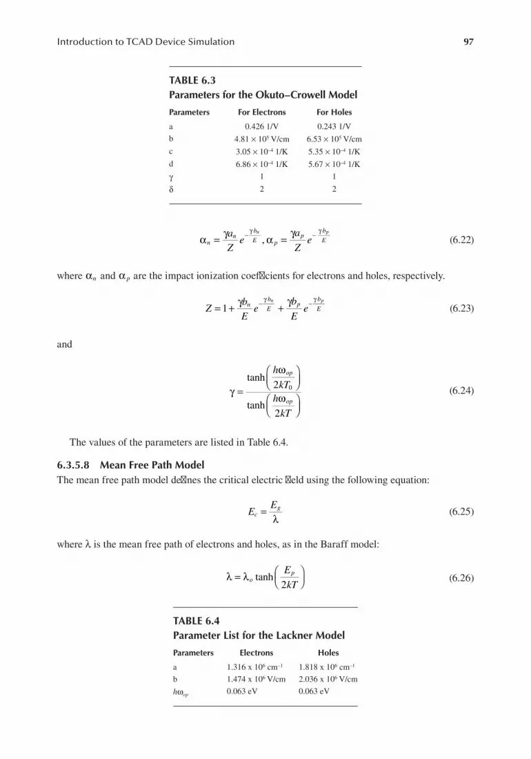
97Introduction to TCAD Device Simulation
α = γ α =
γ−γ
−γa
Ze
a
Zen
nb
E pp
b
En p
, (6.22)
where αn and α p are the impact ionization coefficients for electrons and holes, respectively.
= + γ +
γ−γ
−γ
Zb
Ee
b
Een
b
Ep
b
En p
1 (6.23)
and
γ =
ω
ω
h
kTh
kT
op
op
tanh2
tanh2
0 (6.24)
The values of the parameters are listed in Table 6.4.
6.3.5.8 Mean Free Path ModelThe mean free path model defines the critical electric field using the following equation:
=
λE
Ec
g (6.25)
where λ is the mean free path of electrons and holes, as in the Baraff model:
λ = λ
E
kTo
ptanh2
(6.26)
TABLE 6.3Parameters for the Okuto–Crowell Model
Parameters For Electrons For Holes
a 0.426 1/V 0.243 1/V
b 4.81 × 10⁵ V/cm 6.53 × 10⁵ V/cm
c 3.05 × 10⁻⁴ 1/K 5.35 × 10⁻⁴ 1/K
d 6.86 × 10⁻⁴ 1/K 5.67 × 10⁻⁴ 1/K
γ 1 1
δ 2 2
TABLE 6.4Parameter List for the Lackner Model
Parameters Electrons Holes
a 1.316 x 106 cm–1 1.818 x 106 cm–1
b 1.474 x 10⁶ V/cm 2.036 x 10⁶ V/cm
hωop 0.063 eV 0.063 eV

98 Integrated Power Devices and TCAD Simulation
Ep is the optical phonon energy. Physically, electrons and holes that accelerate in the deple-tion region over a length of λ will gain an energy of λ ⋅E . If this energy is greater than bandgap energy Eg, impact ionization will take place. The mean free path model is similar to Baraff’s model except that Baraff model is more accurate and fits the whole experimental range. Unfortunately, being more complicated means the Baraff model has issues with numerical convergence in TCAD simulations. The mean free path model addresses this issue with a simplified equation. The default parameter table is similar to the Baraff model, as seen in Table 6.5.
6.3.5.9 Multiplication Factor and Ionization IntegralAvalanche breakdown is defined by the impact ionization rate becoming infinite. To allow calcula-tion of the total number of electron–hole pairs generated by a single electron–hole pair at a distance x from the PN junction in the space charge region, a new parameter called multiplication coefficient is derived [158]:
( )
1 ( )
0
0 0
∫∫ ∫
( ) =α −α
− α α −α
M xexp dx
exp dx dx
x
n p
w
p
x
n p
(6.27)
where w is the depletion width. The avalanche breakdown condition is met when the total number of generated electron–hole pairs or ( )M x , goes to infinity. This means
( ) 10 0∫ ∫α α −α
=exp dx dx
w
p
x
n p (6.28)
This expression is known as an ionization integral. If we assume that electrons and holes have the same impact ionization coefficient, or α = α = αn p , then the ionization integral can be rewritten as
10∫α =dx
w
(6.29)
This ionization integral is valid for diodes and MOSFETs where current flowing through the depletion region is not amplified [158]. For BJTs and LIGBTs, current flowing through the depletion region is amplified by a current gain so it is necessary to solve the multiplication coefficient rather than the ionization integral.
TABLE 6.5Parameter List for the Mean Free Path Model
Parameters Values
Electron phonon energy (Ep) 0.063
Hole phonon energy (Ep) 0.063
0 temperature electron optical phonon mean free path (λ0) 76
0 temperature hole optical phonon mean free path (λ0) 58

99Introduction to TCAD Device Simulation
Most device simulators can export or plot the impact ionization coefficient α. However, the ion-ization integral is not easy to evaluate since the path of ionization current may not be a straight line in a 2D/3D simulation. One simplification is to estimate the ionization integral (2D) by
10 0∫ ∫ α
=dxdy
D
D w
(6.30)
where D is the dimension lateral to the direction of E-field (x direction). Many device simulators (including APSYS) provide such a 2D/3D integral of . α
Based on the method of ionization integral as an estimate of breakdown voltage, we can develop a convergence technique as follows. Since impact ionization is a leading cause of divergence in TCAD simulation, we can evaluate the impact ionization term but not use it in the drift-diffusion solver. That is, the impact ionization calculation is treated as a postprocessing step: once the solver has converged, α will be calculated and the ionization integral will be used to determine the breakdown voltage.
6.3.5.10 Critical Electric FieldThe critical field for silicon at which the impact ionization takes place is doping concentration dependent. Several models have been proposed for the critical value. For example:
From [158]:
4010 1/8=E Nc D (6.31)
From [166]:
4 10
113
log10
5
10 16 3
= ×
−
−
ENcm
c (6.32)
A comparison chart is plotted in Figure 6.4. Both models yield similar critical field values until the doping concentration reached 1E+17 cm–3, beyond which a large discrepancy occurs.
Doping Concentration (cm–3)1E161E15
3×10⁵
4×10⁵
5×10⁵
Criti
cal E
lect
ric F
ield
(V/c
m)
6×10⁵
7×10⁵
8×10⁵
9×10⁵ BaligaSze
1E17
FIGURE 6.4 Critical electric field model comparison.

100 Integrated Power Devices and TCAD Simulation
6.3.5.11 Analytical Breakdown VoltageThe method of using ionization integral with impact ionization coefficients to solve the breakdown voltage is most accurate and yet quite often results in a nonclosed form. Numerical iteration is necessary for most impact ionization coefficients models. Sometimes, engineers need a quick and simple estimate of breakdown voltage. The critical electric field is used to directly derive the break-down voltage with calculated depletion width. From Poisson’s equation the breakdown voltage can be expressed with a critical field as [160].
2
2
= ε −BVEqN
Vs cbi (6.33)
Here, Vbi is the built-in potential that can be safely neglected for most cases since it is much smaller than the breakdown voltage. N is the average doping concentration of the N- and P-regions and is calculated as
=
+N
N NN N
a d
a d
(6.34)
Analytical closed-form breakdown voltage calculation is convenient for rough estimates or hand calculations. Several proposed approximations are available.
From Reference [167], assume = ×Ec 5 10 V/cm5 the breakdown voltage is exp ressed as
≈ ×
BV
N15
1017 0.6
(6.35)
From reference [158], the analytical breakdown voltage is calculated by the ionization integral of power law (Fulop’s law) derived impact ionization coefficient
5.34 1013 3/4= × −BV ND (6.36)
with a depletion width calculated as
2.67 1010 7/8= × −W ND (6.37)
6.3.5.12 Benchmark Comparison of Avalanche Breakdown ModelsTo give the reader a better view of different models for avalanche breakdown, both TCAD numerical simulations and analytical models are used to make a comparison. A P+/N junction is used. The highly doped P+ region has a constant doping concentration of 1E+20 cm–3, with abrupt parallel junction. The doping concentration in the N-region varies from 5E+14 cm–3 to 5E+17 cm–3 as seen in Table 6.6. Figure 6.5 plots the resulting curves. Note that TCAD simulated breakdown voltages are higher than analytical results due to mesh roughness and more realistic depletion profiles.
6.3.6 cArrier moBility
The carrier mobility µn and µp account for the scattering mechanism in electrical transport. One of the main effects on the mobility is the local electrical field [138].

101Introduction to TCAD Device Simulation
6.3.6.1 Models OverviewCommon analytical formulas for field-dependent mobility [156] are defined in this section:
• Constant mobility model• Two-piece mobility model• Canali or beta model• Transferred electron model• Poole–Frenkel field enhanced mobility model• Impurity dependence of the low field mobility model• Intel’s local field models• Lombardi model
6.3.6.2 Constant MobilityThe simplest mobility model uses constant mobility µ0n and µ0p for electrons and holes, respectively, throughout each material region in the device. This model is very simple but inaccurate.
TABLE 6.6Benchmark Comparison of Breakdown Models Using the P+/N Parallel Plane
N-region Doping Conc. (cm–3)
Baliga (V) [158]
Hu (V) [167]
Chynoweth (V)
Baraff (V)
Lackner (V)
MeanfreePath (V)
5.00E+14 505 360 494 486 521 519
1.00E+15 300 238 316 293 334 304
5.00E+15 90 91 109 89 113 101
1.00E+16 53 60 72 55 73 65
5.00E+16 16 23 31 20 31 27
1.00E+17 9.5 15 23 14 23 19
1E16 1E17
BaligaHu
MeanfreeLacknerBaraffChynoweth
1E15
10
100
Brea
kdow
n Vo
ltage
(V)
Doping Concentration (cm–3)
FIGURE 6.5 Benchmark comparison of breakdown voltage calculated or simulated by different models.

102 Integrated Power Devices and TCAD Simulation
6.3.6.3 Two-Piece Mobility ModelSince carrier mobility is strongly dependent on an electric field, we can combine a low field model plus a high field model to approximately simulate the field dependent effect. For electrons:
, 0 0µ = µ <for E En n n (6.38)
, 0µ = ≥v
Efor E En
snn (6.39)
0 0= µv Esn n n (6.40)
where 0E n is a threshold field beyond which the electron velocity saturates to a constant. Similar expressions can be defined for holes:
, 0 0µ = µ <for E Ep p p (6.41)
, 0µ = ≥v
Efor E Ep
spp (6.42)
0 0= µv Esp p p (6.43)
6.3.6.4 Canali or Beta ModelThe Canali or beta model [168] is commonly used in the literature and has the following form for electrons and holes, respectively:
1
0
0
1µ = µ
+ µ
β βE
v
nn
n
sn
n n (6.44)
1
0
0
1µ = µ
+ µ
β βE
v
pp
p
sp
p p (6.45)
6.3.6.5 Transferred Electron ModelThe transferred electron model [168] is used in many III-V compound semiconductors, which exhibit negative differential resistance due to the transition of carriers into band valleys with lower mobility [138]:
1
00 0
3
0
4µ =µ +
+
vE
EE
EE
n
nsn
n n
n
(6.46)
6.3.6.6 Poole–Frenkel Field Enhanced Mobility ModelHighly localized carriers with small mobility can be excited by an external field to make hopping movements, commonly used for organic semiconductors:
exp0µ = µ
EEcr
px
(6.47)

103Introduction to TCAD Device Simulation
6.3.6.7 Impurity Dependence of the Low Field Mobility ModelBesides the field dependence of the mobility, another important effect is the impurity dependence of the low field mobility [138].
1
0 12 1
∑µ = µ + µ −µ
++ +
αN N N
N
n nn n
D Aj
tj
rn
n
(6.48)
1
0 12 1
∑µ = µ + µ −µ
++ +
αN N N
N
p pp p
D Aj
tj
rp
p (6.49)
where the various parameters are fitting parameters from experimental data. Some of these values may also be temperature dependent.
6.3.6.8 Intel’s Local Field ModelsIn many applications, the mobility is anisotropic and also depends on the vertical field. A number of vertical field dependent models (e.g., the Lombardi model) are implemented in TCAD device simulators. The anisotropic models are useful for vertical field dependent mobility in MOSFET channel.
The Intel1 and Intel2 models are based on PISCES 2ET manual of Stanford University [169] as follows. The Intel1 model defines a factor rperp to reduce the mobility under the channel:
1= +
⊥−β
rEEperp
crit (6.50)
where ⊥E is the field perpendicular to the SiO2/Si interface. Ecrit is a parameter with value of 4.2E+4 V/cm for electrons and 3E+4 V/cm for holes in silicon. By default, 0.5β = .
The model Intel2 uses the following formula for the reduction factor:
1
1
= +
⊥α −
rE
Eperp
univ
(6.51)
where 1.02α = for electrons, and 0.95α = for holes. Euniv has a value of 5.71E+5 V/cm for elec-trons and 2.57E+5 V/cm for holes. Both of these models are for low-field mobility only.
6.3.6.9 Lombardi ModelA more physics-based model to account for the effect of the transverse field is developed based on extensive experimental data by Lombardi [169] [170]. Basically, this model is to summarize the contributions to mobility from different sources as follows:
1 1 1 1
0µ=µ
+µ
+µac srf
(6.52)

104 Integrated Power Devices and TCAD Simulation
where µac is the mobility due to the acoustic phonon scattering, depending on both transverse field and lattice temperature. µsrf is about surface scattering and is a function of the transverse field. 0µ is the mobility due to the longitudinal field or hot-carrier effect. µac and µsrf are expressed as
13
µ = + α⊥
β
⊥
BE
N
T Eac
L
(6.53)
2µ = δ⊥E
srf (6.54)
The values of the parameters used in Equations (6.53) and (6.54) are listed in Table 6.7.
6.3.6.10 Comparison of Different Diffusion ModelsA comparison between different diffusion models is made using a simple silicon long channel N-type MOSFET structure. As shown in Figure 6.6 two gate voltages (Vg = 5 V and Vg = 1.5 V) are applied, and drain voltage is scanned from 0 to 10 V for both gate voltages. Four mobility models (Canali or beta model, Intel1, Intel2, and Lombardi) are compared. It has been found that for both gate voltages the Canali model yields the highest drain current, which means it predicts the highest electron mobility. This is somewhat expected because the Canali model does not take vertical field-induced mobility reduction into account while other three models are all anisotropic models. The Lombardi model and Intel2 model are relatively close, but the results depend on the gate voltage. Default model parameter values are used for all simulation cases.
6.3.6.11 GaN Mobility Model (MTE Model)A modified transferred-electron mobility model designed for GaN devices is proposed by [168]. It has been found that GaN has a very specific drift velocity dependence on the electric field. A qualitative comparison (not drawn to scale) is shown in Figure 6.7. Different from silicon (where the Canali model can be applied), GaN has a negative differential mobility region similar to that of GaAs. However, GaN also has a kink at low field, which makes direct use of transferred-electron mobility model insufficient. A modified transferred-electron (MTE) mobility model is thus required to model GaN mobility. Based on the transferred-electron model, a more universal model should be like [168].
1
( )( )
=+
+
β
βv EF E v
EE
EE
MTE
satMT
MT
T
T (6.55)
TABLE 6.7Parameter Values for μac and μsrf
B α β δElectrons 4.75E+7 1.74E+5 0.125 5.82E+14
Holes 9.93E+7 8.84E+5 0.0317 2.05E+14

105Introduction to TCAD Device Simulation
Drain Voltage (V)
Dra
in C
urre
nt (A
/m)
Dra
in C
urre
nt (A
/m)
(c) Id – Vd curve at Vg = 5 V with different mobility models
(a) A simple long channel MOSFET (b) Net doping of the long channel MOSFET
(d) Id – Vd curve at Vg = 1.5 V with differentmobility models
00
100
200
300
400
500
–3–1.5 –1 –0.5 0 0.5 1 1.5 –1.5 –1 –0.5 0 0.5 1 1.5
Material Number
(donor_conc/acceptor_conc/)Signed_Log10
Poly
SiSio2
–2.5
–2
–1.5
–1
–0.5
0
–3
–2.5
–2
–1.5
–1
–0.5
0
I-V Curves Comparison between Different Mobility Models
OxidePoly
Silicon
N-LDDN+
(source/drain)
20.40312015105
–5–10–15–16.7422
0
P-body
40
35
30
25
20
15
10
5
00 2 4
Drain Voltage (V)6 8 10
Canali modelIntel1 modelIntel2 modelLombardi model
Canali modelIntel1 modelIntel2 modelLombardi model
2 4 6 8 10
FIGURE 6.6 Comparison of different mobility models using a long channel MOSFET.
(c) Electron drift velocityof GaN
(b) Electron drift velocityof GaAs
(a) Electron drift velocityof silicon
Electric Field
Silicon GaAsNegative Differential
MobilityNegative Differential
Mobility
GaN
Electron Drift Velocity Plots for Si, GaAs and GaN Materials
Elec
tron
Drif
t Vel
ocity
Elec
tron
Drif
t Vel
ocity
Elec
tron
Drif
t Vel
ocity
Electric Field Electric Field
Kink at low field
FIGURE 6.7 Qualitative comparison of electron drift velocity in silicon, GaAs, and GaN materials.

106 Integrated Power Devices and TCAD Simulation
where ( )F E is used to mimic the low field kink effect to allow a smooth transition from low field slop (µlow ) to high field slop (µhigh) and is expressed as
1( )
1( ) = µ
+ µµ −µ +µ
β β
F EE
EE E
low
low
low high k high
k k (6.56)
Ek is defined as
11
11
=µ
⋅ µµ − µ
⋅ µµ
−
+ δ
β+β
β+
Ev
Eksat
low
high
low high
low
highk
c
c
c
(6.57)
Some of the parameters in the MTE model are listed in Table 6.8 [168] [171] [172].
6.3.7 tHermAl And selF-HeAting
For power semiconductor device simulations, thermal and self-heating effects are a major concern. The heat generation often limits what a designer can do with a passively cooled device and the max-imum power that can be reached. TCAD simulation includes temperature-dependent simulation for bandgap, mobility, recombination coefficients, and other material parameters. When the self-heating models are not turned on, the simulation will default to isothermal temperature profiles.
6.3.7.1 Heat Flow and Temperature DistributionIn terms of simulation, one needs to figure out the temperature distribution from all possible heat sources. This often means considering a much larger simulation area than the small region near the PN junction as we must think about how the heat flows through the whole substrate as well as from any wire bonds. We must also examine how the heating affects the device performance, which means gathering as much data as possible on the temperature dependence of important material parameters. This is not a trivial task because virtually all variables and material parameters are temperature dependent. It is not immediately obvious which ones are most important, but in general bandgap and mobility should be at the top of this list.
TABLE 6.8Some Parameters for the MTE Model
Parameters Ref [171] Ref [172]
µhigh cm2/V s 100 133.3
vsat 1E+7 cm/s 1.91 1.44
EMT kV/cm 257 195
βc 1.7 3.2
βT 5.7 3.9
βk 4 4
δEk kV/cm 0 5

107Introduction to TCAD Device Simulation
We are concerned with the generation and flow of lattice heating power in a semiconductor, so we first consider the heat flux and then the heat source. We introduce the thermal conductivity such that the heating power flux (in Watt/m2) is given by
= −κJ Th (6.58)
Conservation of energy requires that the temperature distribution satisfy the following basic thermal equation:
ρ ∂∂
= − ⋅ +CTt
J Hp h (6.59)
or
ρ ∂∂
= ⋅κ +CTt
T Hp (6.60)
where Cp is the specific heat, ρ is the density of the material, and H is the heat source.The goal of TCAD thermal simulation is to provide a thermal modeling environment so that all
possible sources of temperature dependence can be taken into account. Many different sources of heat are included in TCAD tools including joule heating from the current flow and recombination heat from the carriers interacting with defects. Consult the software’s manual for more details on the models that are included.
6.3.8 BAndgAp nArrowing eFFect
It is observed experimentally that the shrinkage of bandgap occurs when impurity concentration is high (e.g., 1017>nimp cm–3). This is called the bandgap narrowing effect, which is ascribed to the emerging of the impurity band formed by the overlapped impurity states. The bandgap narrowing model proposed by Slotboom is given by
ln 0.52= + +
E E
n
nln
n
ng ref
imp
ref
imp
ref (6.61)
where Eref , nref , and nimp represent energy parameter, density parameter, and impurity concentra-tion, respectively. For silicon, Eref and nref were obtained by fitting the experimental result, which yields
0.009 =E Vref (6.62)
10 17 3= −n cmref (6.63)
It should be noted that the bandgap narrowing effect is the doping-dependent effect, while the many-body effect, which can also reduce bandgap, is carrier dependent and thus depends on the applied bias.

108 Integrated Power Devices and TCAD Simulation
6.4 AC ANALYSIS
6.4.1 introduction
Most power semiconductor devices are driven under some sort of AC condition, and many of the device parameters (e.g., capacitance) are measured at a given frequency. Therefore, it is beneficial to have some basic understanding of how TCAD software performs AC analysis. We shall dedicate this section to the theory and application of AC analysis.
AC small signal analysis for semiconductor equations was first developed by Laux [173] in 1985. A modified version of this technique, including the deep level trap model, was later developed by Li and Dutton [174]. We shall follow their formulation in this section.
The basic problem of AC analysis is stated as follows: for a device at a given DC (or quasi-DC for slow transient cases) bias, how would the device behave if one or more device contacts were subject to an AC voltage signal of the form ξ ωei t , where the modulation amplitude ξ is much smaller than the DC bias.
6.4.2 BAsic FormulAs
We rewrite the basic semiconductor equations including the trap dynamic model as follows:
ε ε(1 ) ( ),0 ∑− ⋅
= − + + − − + δ −
qV n p N f N f N fdc
D D A A
j
tj j tj (6.64)
∑ ( )⋅ − − − − + = ∂
∂+ ∂
∂J R R R R G t
n
tN
f
tn
j
ntj
sp st au opt DD , (6.65)
,∑ ( )⋅ + + + + − = − ∂∂
+ ∂∂
J R R R R G tpt
Nft
p
j
ptj
sp st au opt AA
(6.66)
− = ∂
∂R R N
f
tntj
ptj
tjtj (6.67)
where
1 ,1( )= − −R c nN f c n N fn
tjnj tj tj nj j tj tj (6.68)
1 .1 ( )= − −R c pN f c p N fp
tjpj tj tj pj j tj tj (6.69)
The basic variables involved in the AC analysis are V, the potential; n and p, the electron and hole concentrations, respectively; and ftj, the trap occupancy of the jth trap. To simplify our derivation, we use the following notation to represent Equations (6.64) to (6.67):
( , , , ) 01 =F V U U fn p tj (6.70)
( , , , )2 =
∂∂
+ ∂∂
∂∂
F V U U fn
UN
fU
Ut
n p tjn
DD
n
n (6.71)

109Introduction to TCAD Device Simulation
= − ∂∂
+ ∂∂
∂∂
F V U U fp
UN
f
U
U
tn p tj
pA
A
p
p( , , , )3 (6.72)
, ,( ) = ∂
∂H U U f N
f
tj n p tj tj
tj (6.73)
where we have changed the variables n and p into Un and U p , the normalized quasi-Fermi levels, respectively. For the electron or hole transport equations ( 2F or 3F ) the first term on the right-hand side (RHS) corresponds to ∂n/∂t or ∂p/∂t, while the second term is the response due to the trap fill-ing and emptying.
In general, the AC input signal (voltage) and solution variables are expressed as
0ξ = ξ + ξ ωei t (6.74)
where 0ξ is the DC solution, ξ is the complex AC solution, and 2ω = πf is the modulation fre-quency. ξ can represent V, U Un p , , or ftj as complex solutions. By substituting ξ back into the trap equation and doing a Taylor series expansion to first order around the DC solution, Equation (6.67) becomes
∂∂
+ ∂∂
+ ∂∂
= ωH
UU
H
UU
H
ff N i fj
nn
j
pp
j
tjtj tj tj (6.75)
and solving for ftj gives
1
=∂∂
+ ∂∂
ω − ∂∂
−
fH
UU
H
UU N i
H
ftjj
nn
j
pp tj
j
tj (6.76)
( )2
2=− ∂∂
∂∂
+ ω
− ∂∂
∂∂
+ ω
ω +∂∂
f
H
U
H
fi N U
H
U
H
fi N U
NH
f
tj
j
n
j
tjtj n
j
p
j
tjtj p
tjj
tj
(6.77)
which can be rewritten for simplicity as:
( ) ( )= ω + ωf F U F Utj n n p p (6.78)
Similarly expanding the Poisson equation, electron and hole continuity equations as a first-order Taylor Series, we get
V 01 1 1 1 ( )∂
∂+ ∂∂
+ ∂∂
+ ∂∂
+ =FV
FU
UF
UU
Ff
F U F Un
np
ptj
n n p p (6.79)
V ( )2 2 2 2∂
∂+ ∂∂
+ ∂∂
+ ∂∂
+ =∂∂
+ ∂∂
ωF
VFU
UFU
UFf
F U F Un
UN
fU
i Un
np
ptj
n n p pn
DD
nn (6.80)
V3 3 3 3 ( )∂
∂+ ∂∂
+ ∂∂
+ ∂∂
+ = − ∂∂
+ ∂∂
ωF
VFU
UFU
UFf
F U F Up
UN
fU
i Un
np
ptj
n n p pp
AA
pp (6.81)

110 Integrated Power Devices and TCAD Simulation
We rewrite these three equations in a 3 by 3 matrix form as
0( )+ ξ =J D (6.82)
For each mesh point in the semiconductor the J matrix or Jacobian contains the first three terms in each equation, while D contains the remaining terms concerning the traps and RHS of the equa-tion. Using this notation with ( , , ) ξ = V U Un p the D matrix at each point is of the form
0 ( ) ( )
0 ( ) ( )
0 ( ) ( )
1 1
2 2
3 3
=
∂∂
ω ∂∂
ω
− ∂∂
+ ∂∂
ω + ∂
∂ω ∂
∂ω
∂∂
ω − − ∂∂
+ ∂∂
ω + ∂
∂ω
D
Ff
FFf
F
nU
Nf
Ui
Ff
FFf
F
Ff
Fn
UN
fU
iFf
F
tjn
tjp
nD
D
n tjn
tjp
tjn
nA
A
p tjp
(6.83)
Consider the boundary points and the internal mesh points separately so that
− > +J j JB (6.84)
and
− > +D D DB (6.85)
The matrix equation can then be rewritten in a separated form for internal and boundary mesh points as follows:
0( )( )+ ξ + + ξ =J D J DB B B (6.86)
AC Dirichlet boundary conditions imply that Un and 0=U p so that the AC voltage input at the contact has the boundary solution
00
ξ =
V
B
B
(6.87)
where VB is the applied AC voltage of one volt. Since the first column in the D matrix must be zero, the matrix equation becomes
( )+ ξ = − ⋅ξ ≡J D J BB B (6.88)
To create real-valued equations, the D and ξ complex matrices are written with the real and imaginary components separated:
= +D D iDr i (6.89)
ξ = ξ + ξir i (6.90)

111Introduction to TCAD Device Simulation
The matrix is thus rewritten as
( )( )+ + ξ + ξ =J D iD i Br i r i (6.91)
Equating real and imaginary components provides the two equations
( )+ ξ − ξ =J D D Br r i i (6.92)
0( )ξ + + ξ =D J Di r r i (6.93)
which can be rewritten as the expanded matrix
+ −+
ξξ
=
J D D
D J DB
r i
i r
r
i (6.94)
6.4.3 Ac AnAlysis in tcAd
Our task has been reduced to solving the expanded matrix equation detailed in the previous
subsection. The AC solution matrix ξξ
r
i can be easily solved using a sparse matrix inverter to
invert the expanded Jacobian and multiply by the matrix on the RHS. The inversion can be slow because the expanded Jacobian J + D is twice the order of original J matrix obtained from the DC solution.
In most TCAD software (e.g., APSYS from Crosslight Software), the AC analysis is imple-mented as a postprocessor; that is, the analysis is done after the DC solution is obtained from the main solver input file (with the .sol extension). This is done in the following steps:
• The AC analysis matrix is constructed from Jacobian matrix elements used for DC simula-tion. Or in other words, the DC matrix is saved for later AC analysis.
• After the DC simulation, the AC analysis is activated by an AC analysis command defining which contact to apply the AC voltage and at what frequency range. For C-V simulation, one would fix the frequency at 1 megahertz and would define the DC bias range.
• Use various related TCAD commands to plot the AC conductance or AC capacitance. If necessary, various two-port parameters, such as Y-parameters or S-parameters, can be plotted.
As stated earlier, the basic problem of AC analysis is to study how the device would respond if a contact is subject to an AC voltage signal.
The basic responses are the complex AC currents at all the electrodes and the AC current dis-tribution within the device. Once we have the AC current, the following important quantities can be extracted:
• The conductance matrix elements (such as transconductance) are computed from the real part of the electrode AC current with unit AC voltage applied at one of the electrodes.
• The capacitance matrix elements are computed from the imaginary part of the electrode AC current, divided by ω, with unit AC voltage applied at one of the electrodes.
• The current gain can be computed from the ratio of the AC current magnitudes between two electrodes, with a small AC voltage applied at one of the electrodes.

112 Integrated Power Devices and TCAD Simulation
6.5 TRAP MODEL IN TCAD SIMULATION
As in most wide-gap compound materials, undoped GaN exhibits semi-insulating behavior due to the existence of deep-level traps. It is also believed that gate leakage, reliability, or degradation behaviors of GaN high electron mobility transistors (HEMT) are associated with surface traps. For proper understanding and analysis of GaN power devices, it is necessary to have some basic knowl-edge of how traps are modeled in TCAD simulation.
6.5.1 trAp-cHArge stAtes
A carrier trap can be completely described by trap density, charge state (donor or acceptor), energy level, electron, and hole capture coefficients.
Referring to the schematic of Figure 6.8, a trap has the charge property of being a donor or an acceptor. In the extreme case of energy level of a trap being close to the band edges, traps are no different than common dopants such as boron or arsenic in silicon. To be more specific, the space charge caused by the trap is either 1( )−N ft t for a donor trap or −N ft t for an acceptor trap. Here, Nt and ft are trap density and trap occupancy, respectively. In TCAD, these charge terms appear in the Poisson’s equation along with the other charge terms: shallow dopants; free electrons/holes; and fixed bulk/surface charges.
As far as charge states are concerned, traps are similar to the usual intentional dopants such as boron or arsenic in silicon technology. They can be used to control the Fermi levels, and donors and acceptors can compensate each other. The formation of semi-insulating compound materials is caused by this compensation mechanism: the existence of both deep donors and deep acceptors pins the Fermi level near the middle of the bandgap, and this causes the high resistance of undoped substrate compound materials.
In silicon technology, traps are less important because their densities are low compared with intentional dopants. Since the charge contribution of deep-level traps in silicon is small, their charge states are usually ignored and a single minority lifetime is used to characterize traps in silicon TCAD simulation.
6.5.2 trAp dynAmics
The charge attributes of traps are relatively easy to understand and control in TCAD simulation. The dynamics of traps is far more complicated, and this section is dedicated to the description
Valance Band Ev
e–e–e–
Conduction Band Ec
HoleCapture (cpp)
HoleEmission (cpp1)
ElectronEmission (cnn1)
ElectronCapture (cnn)
FIGURE 6.8 Schematic view of donor traps.

113Introduction to TCAD Device Simulation
and understanding of trap dynamics. Dynamics refers here to the time-dependent behavior such as trapping, detrapping rates, and AC small signal analysis. The AC analysis is especially important since the existence of a large amount of deep-level traps strongly affects the AC capacitance and conductance of a GaN-based power device.
Our approach is to assume some simplified situation where traps are dominant in the drift-diffusion equation. We then derive capacitance and conductance of a semiconductor region and analyze their behavior. Finally, we set up a TCAD simulation to compute AC capacitance and conductance to confirm the simplified trap dynamic theory.
We introduce the trap dynamic equation (or sometime called trap rate equation) as follows:
= −N
dfdt
R Rtt
n p (6.95)
1 1( )= − −R c nN f c n N fn n t t n t t (6.96)
11 ( )= − −R c pN f c p N fp p t t p t t (6.97)
where Nt is the bulk trap density; Rn and Rp are the bulk recombination rates for electrons and holes, respectively; cn is the capture coefficient, which can be further expressed in terms of thermal velocity and capture cross section, ,= σc vn th n n ; and 1n is the electron density when the Fermi level coincides with the trap level. Similar quantities are given for holes.
As a good exercise, one can prove that at the steady state, =R Rn p (or / 0=df dtt ), and by solv-ing the trap occupancy ft , the recombination rate reduces to the more familiar Shockley–Read–Hall recombination rate.
Usually, there is more than one kind of trap in the system, and we add a trap index j in Equations (6.95)–(6.97), such as Ntj or ftj . For simplicity we drop the trap index in the discussion while keep-ing in mind that the theory applies to all other traps.
The simplified situation is that we consider a region with substantial amount of traps (e.g., 1E+17 cm–3). There is only light intentional doping, or it is totally undoped. The free carriers are supplied via injection from nearby contacts. In Appendix C, we will derive the small signal AC current flow-ing through this region under AC voltage ΔV. The AC current can be expressed as
= + ωI G V j C Vtp tp (6.98)
where the conductance Gtp is given by
( )
2
20 0
2=ω
ω + +G
V NdcdV
c n c ptp
tp ti
n p
(6.99)
and the capacitance is obtained as
( )
( )
0 0
20 0
2=
+
ω + +C
V NdcdV
c n c p
c n c ptp
tp ti
n p
n p
(6.100)

114 Integrated Power Devices and TCAD Simulation
where n0 and p0 are the steady-state electron and hole concentrations, respectively; Vtp is the volume of the trap region; and ci is a parameter depending on carrier injection.
It is interesting to note that the frequency response of capacitance and conductance are comple-mentary: the capacitance peaks on the lower frequency side, while the conductance peaks on the higher side. Furthermore,
frequency _ independent _ constant+ =C Gtp tp (6.101)
The characteristic frequency for the peaks is given by 0 0+c n c pn p , and it is dependent on carrier density and trapping rate. Due to the existence of more than one kind of trap in the system, the AC behavior is not simple to predict.
We demonstrate the AC TCAD simulation using APSYS in the following structure. An AlGaN/GaN diode is built with Al mole fraction of 0.1 for AlGaN (A10.1Ga0.9N). A10.1Ga0.9N is P doped with doping concentration of 1E+17 cm-3 and GaN is N doped with doping concentration of 1E+17 cm–3, as seen in Figure 6.9.
Donor-type traps located at 1.2 eV below conduction band are placed within GaN material with trap concentration of 5E+17 cm-3; the capture cross section is 1E-15 cm-2. The same structure with-out traps is also simulated as a comparison. A positive DC bias is applied to the cathode (GaN side) for both diode devices.
The capacitance and conductance in Figure 6.10 show the predicted complementary profile with capacitance peaks at the lower frequency side. In a real device, the number of traps and traps levels are rather complex and it is not easy to judge whether or not trap regions are the dominant factor in the device characteristics. Our theory here may help in two ways.
1. If a material is well-known to have deep-level traps (e.g., near the substrate), the TCAD can help determine if such traps would have an impact to the AC capacitance and conductance.
2. If frequency response peaks are measured in the lower end of capacitance or higher end of conductance that cannot be easily explained by simple junction or depletion region theory, then traps may be the cause, and one may use reverse engineering to deduce the existence of traps in one or more regions of the device.
(b) Net doping plot of AlGaN/GaN diode(a) Material plot of AlGaN/GaN diode
0.80.60.40.200
0.2
0.4
0.6
0.8
1+Y +Y
AnodeAl0.1Ga0.9N
Al0.1Ga0.9N
GaN
Net_Doping–17 –15 –10 –5 0 5 10 15 17
N doping = 1E+17 cm–3
P doping = 1E+17 cm–3
FEM_Structurealgan(x = 0.1)gan
GaNCathode
Simulation Structure Views of GaN Traps Example
1 0.80.60.40.200
0.2
0.4
0.6
0.8
1
1
FIGURE 6.9 Simulation structure views of the AlGaN/GaN diode to demonstrate how traps influence device performance.
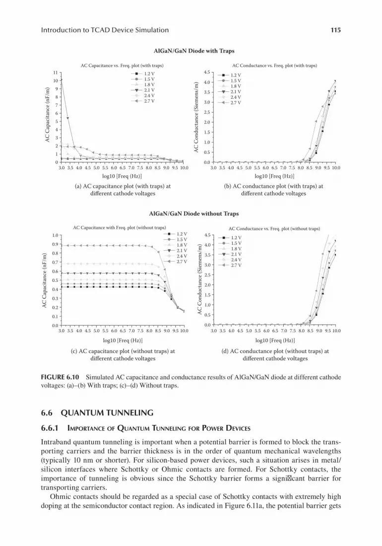
115Introduction to TCAD Device Simulation
6.6 QUANTUM TUNNELING
6.6.1 importAnce oF QuAntum tunneling For power devices
Intraband quantum tunneling is important when a potential barrier is formed to block the trans-porting carriers and the barrier thickness is in the order of quantum mechanical wavelengths (typically 10 nm or shorter). For silicon-based power devices, such a situation arises in metal/silicon interfaces where Schottky or Ohmic contacts are formed. For Schottky contacts, the importance of tunneling is obvious since the Schottky barrier forms a significant barrier for transporting carriers.
Ohmic contacts should be regarded as a special case of Schottky contacts with extremely high doping at the semiconductor contact region. As indicated in Figure 6.11a, the potential barrier gets
log10 [Freq (Hz)]
AC C
ondu
ctan
ce (S
iem
ens/
m)
AC C
apac
itanc
e (nF
/m)
AC C
apac
itanc
e (nF
/m)
10.09.59.08.58.07.57.06.56.05.55.04.54.03.53.0
log10 [Freq (Hz)]
10.09.59.08.58.07.57.06.56.05.55.04.54.03.53.00.0
0.1
0.2
0.3
1.0
1110
876543210
9
0.9
0.8
0.7
0.6
0.5
0.4
0.0
0.5
1.0
1.5
2.0
2.5
3.0 2.7 V2.4 V2.1 V1.8 V1.5 V1.2 V
2.7 V2.4 V2.1 V1.8 V1.5 V1.2 V
2.7 V2.4 V2.1 V1.8 V1.5 V1.2 V
2.7 V2.4 V2.1 V1.8 V1.5 V1.2 V
AC Conductance vs. Freq. plot (without traps)
(d) AC conductance plot (without traps) atdifferent cathode voltages
(c) AC capacitance plot (without traps) atdifferent cathode voltages
(a) AC capacitance plot (with traps) atdifferent cathode voltages
AlGaN/GaN Diode without Traps
AlGaN/GaN Diode with Traps
AC Capacitance with Freq. plot (without traps)
AC Capacitance vs. Freq. plot (with traps) AC Conductance vs. Freq. plot (with traps)
3.5
4.0
4.5
log10 [Freq (Hz)]
AC C
ondu
ctan
ce (S
iem
ens/
m)
3.0 3.5 4.54.0 5.55.0 6.56.0 7.0 7.5 8.58.0 9.59.0 10.0
log10 [Freq (Hz)]3.0 3.5 4.54.0 5.55.0 6.56.0 7.0 7.5 8.58.0 9.59.0 10.0
(b) AC conductance plot (with traps) atdifferent cathode voltages
0.0
0.5
1.0
1.5
2.0
2.5
3.0
3.5
4.0
4.5
FIGURE 6.10 Simulated AC capacitance and conductance results of AlGaN/GaN diode at different cathode voltages: (a)–(b) With traps; (c)–(d) Without traps.

116 Integrated Power Devices and TCAD Simulation
narrower as doping is increased. In the extreme of high doping, the barrier is so thin that the current flows through the barrier easily with a large tunneling coefficient (see Figure 6.11b).
A common approach to modeling a good Ohmic contact is to assume the barrier does not exist and the band diagram is flat. This can be achieved by artificially adjusting the metal work func-tion so that the metal Fermi level aligns with the semiconductor band edge. Since different TCAD software may treat the metal differently, when using a metal layer on a semiconductor one should always examine the band diagram near the metal/semiconductor junction to ensure the Schottky or Ohmic contacts have the expected band alignment.
For AlGaN/GaN power devices, in addition to the tunneling at Schottky/Ohmic contacts, one must also consider tunneling through a heterojunction or a whole barrier layer. The current flowing through a highly doped heterojunction can get rather complicated since high doping can create a highly depleted layer in the barrier and cause a large voltage drop there unless quantum tunneling is activated. We consider an AlGaN/GaN heterojunction subject to different densities of n-doping. As indicated by Figure 6.12a, the tunneling barrier gets thinner at higher doping, similar to the situation of Schottky/Ohmic contacts. The current computed using tunneling theory is indicated in Figure 6.12b, indicating much higher reverse current for higher doping.
One can show that the barrier height at high doping is dependent on whether there is a compo-sition grading at the heterojunction. The highest barrier is obtained for an abrupt junction while composition grading reduces or even completely removes the potential barrier at high doping. If the details of transport in the highly doped heterojunction are not important and one wishes to avoid dealing with tunneling, a shortcut would be to artificially grade the abrupt heterojunction to remove the high barrier.
6.6.2 BAsic tHeory oF tunneling For tcAd simulAtion
As discussed in previous subsections, there are ways to avoid the use of tunneling for highly doped heterojunctions or Ohmic contacts if the details of transports are not important. For barriers where tunneling is of primary importance, we need to formulate the tunneling theory in a simple way that TCAD software can employ.
In quantum mechanics, tunneling depends on carrier distribution as a function of kinetic energy. Since drift-diffusion theory is based on the assumption that carriers assume a Fermi–Dirac
(b) Reverse bias current with tunnelingactivated at various N-doping
(a) Silicon-gold Schottky barrier conductionband profile at various N-doping
Rev. Bias (V)Distance (um)10.950.90.850.8 1.05 1.1
Curr
ent (
A/m
)
1.61.41.210.80.60.40.201e–007
1e–006
1e–005
0.0001
0.001
0.01
0.1
1
10
100
Schottky Barrier and Tunneling at Various N-Doping
2.5
1.5
0.5
0
1
21E+19 cm–3
1E+19 cm–3
1E+18 cm–3
1E+18 cm–3 1E+17 cm–3
1E+17 cm–3
Cond
uctio
n Ba
nd (e
V)
FIGURE 6.11 (a) Silicon–gold Schottky barrier conduction band profile at various n-doping; (b) Reverse bias current with tunneling activated at various n-doping.

117Introduction to TCAD Device Simulation
distribution (quasi-equilibrium), a reasonable approach for quantum tunneling is to assume that car-riers incident upon the barrier follow this distribution.
The formulas we use here are based on quasi-equilibrium approximations, and the approach is similar to that used by Grinberg et al. [175]. Since carriers at the top of the barrier are not blocked, it is sufficient we calculate the current flow at the top of the barrier.
We use the schematic in Figure 6.13 and consider the drift current on top of the barrier Xm :
= + αJ qvn qvnm m T (6.102)
where αT is the tunneling coefficient to be derived. The velocity v is dependent on mobility or the thermionic emission properties at the top of the barrier.
Here the basic understanding is that the quasi-Fermi level is relatively flat around the bar-rier such that the energy distribution of the carriers can be expressed by a simple Boltzmann function (or exponential function) since the Fermi level is usually far below the top of the barrier. We assume that the carriers with energy between 0U and Um are capable of tunneling
(a) AlGaN/GaN heterojunction conductionband profile at various N-doping
Distance (um)
1.81.61.41.2
0.8
Cond
uctio
n Ba
nd (e
V)
0.60.40.2
0.8 0.85 0.9 0.95 1 1.05 1.1Rev. Bias (V)
0 0.2 0.4 0.6 0.8 1 1.2 1.4 1.60
1
Heterojunction and Tunneling at Various N-Doping
1E+17 cm–3
1E+19 cm–3
1E+18 cm–3
1E+17 cm–3
1E+18 cm–3
1E+19 cm–3
(b) Reverse bias current with tunnelingactivated at various N-doping
10000
1000
100
10
0.1
0.01
1Curr
ent (
A/m
)FIGURE 6.12 (a) AlGaN/GaN heterojunction conduction band profile at various n-doping; (b) Reverse bias current with tunneling activated at various n-doping.
X1 Xm X2
U1
U0
Um
Pote
ntia
l
E
X
FIGURE 6.13 Schematic of the potential barrier for tunneling theory.

118 Integrated Power Devices and TCAD Simulation
through the barrier and appears on the other side, giving rise to the additional term in Equation (6.102). For carriers with energy greater than Um , they are accounted for by the standard drift-diffusion model.
We define an energy-dependent carrier distribution nE such that
∫=n n dEE (6.103)
Using Boltzmann distribution
( )exp= −
n g E
U EkT
Em
(6.104)
where ( )g E is the density of states that is a much slower function of energy than the exponential function. For numerical convenience, we ignore the slower energy dependence and replace it by an average constant nEm so that Equation (6.103) still holds. As we shall see later, our final results do not depend on the choice of constant nEm .
Since we are able to express the energy distribution as
exp= −
n n
U EkT
E Emm (6.105)
the tunneling current can be expressed as
∫ ∫( ) ( )= = −
J qvn D E dE qvn
U E
kTD E dEtun
U
U
E T Em
U
U
mT
m m
exp
0 0
(6.106)
where ( )D ET is the energy-dependent tunneling transparency. We note that the carrier density at the top of the potential barrier can be expressed in term of nEm:
exp∫= −
=
∞
n nU E
kTdE n kTm
U
Emm
Em
m
(6.107)
Therefore, the tunneling current can be written as
( ) exp1
0
∫ ( )= −
−J qvn kTU E
kTD E dEtun m
E
U
mT
m
(6.108)
The tunneling coefficient αTm at the top of the barrier is given by
∫ ( )α = −
−kTU E
kTD E dETm
E
U
mT
m
( ) exp1
0
(6.109)
The main task of computing the tunneling current has been reduced to calculation of the energy-dependent tunneling transparency ( )D ET . A commonly used method for computation of tunneling

119Introduction to TCAD Device Simulation
transparency is the transfer matrix method (TMM) or the propagation matrix method, which cuts up an arbitrary potential profile into piecewise constant barriers. For each of the constant barriers, a 2 × 2 matrix describing forward and backward traveling waves can be constructed. The total trans-parency can be obtained by multiplying the 2 × 2 matrices.
The previous formulas are relatively easy to implement in TCAD software and were used by the APSYS software package from Crosslight Software.
6.6.3 introduction to noneQuiliBrium green’s Function For tunneling
The previous subsection describes the equilibrium theory of quantum tunneling, which is consistent with the drift-diffusion theory. The latest simulation technology may employ the nonequilibrium Green’s function (NEGF) method for tunneling. Due to the complexity of the NEGF, only a conceptual introduction is given here referring to the equilibrium theory we have described previously.
In the quasi-equilibrium theory, the system can be described by the Fermi level and carrier dis-tribution in the whole tunneling region is described by Fermi or Boltzmann functions. The NEGF method does not assume such Fermi or Boltzmann distribution and Fermi levels are not used.
The NEGF solves for the Green’s function, a correlation function relating the probability of finding a carrier at one position with another. The Green’s function is solved in spatial, momentum, and energy coordinates and can take into account of various scattering mechanisms such as phonon scattering while tunneling. Some advanced TCAD packages (such as APSYS from Crosslight) have implemented NEGF and interested readers should consult the relevant documentations.
6.7 DEVICE SIMULATOR MODELS CALIBRATION
As mentioned in Section 5.9, the accuracy of TCAD simulation depends on how well the models in the process and device simulators are calibrated for a particular set of equipment and fabrication facilities. In this section, a general approach to calibrate the models for a device simulator will be discussed.
Assuming that the process simulator has been calibrated in the first place, the device simu-lator has to be calibrated such that the electrical characteristics or parameters of the simulated device can be as close as possible to those of the experimental device. For example, in the case of a metal-oxide-semiconductor field-effect transistor (MOSFET), important electrical characteristics for calibration include the drain current versus gate voltage curves at constant drain voltage, the on-state drain current versus drain voltage curves at various gate voltages, and the off-state drain current versus drain voltage curve at zero gate voltage. Electrical parameters of the MOSFET can be extracted from these electrical curves. For example, threshold voltage can be extracted from the drain current versus gate voltage curves. Moreover, on-state resistance, saturation current, and on-state breakdown voltage can be extracted from the on-state drain current versus drain voltage curves. Finally, off-state breakdown voltage and leakage current can be extracted from the off-state drain current versus drain voltage curve. A well-calibrated device simulator is able to predict elec-trical characteristics at arbitrary bias conditions such that the discrepancy between the simulated and measured device performance is acceptable. However, if the discrepancy persists after con-siderable effort has been put in calibrating the device simulator, calibration of the corresponding process simulator will have to be reviewed [142].
Calibration of a popular device simulator, Medici [176], for MOSFET simulation is illustrated as an example. It begins with calibrating the simulated drain current versus gate voltage curve with the corresponding measured curve [177]. The drain current in the linear region is mainly determined by the carrier mobility, whereas the threshold voltage is determined by several parameters such as the gate metal work function and the interface charges. All of these parameters can be adjusted in

120 Integrated Power Devices and TCAD Simulation
the device simulator. It is followed by calibration of the on-state drain current versus drain volt-age curves. The on-state resistance, saturation current, and on-state breakdown voltage are mainly determined by the carrier mobility, saturation velocity, and impact ionization rate, respectively. For the case of a power MOSFET, which operates at high power in the on-state, modeling of thermal effect and lattice heating have to be enabled in the device simulator for a more precise calibration. Finally, the leakage current and off-state breakdown voltage, which can be extracted from the off-state drain current versus drain voltage curve are mainly determined by the band-to-band tunneling and impact ionization rate, respectively. Both of these parameters can be adjusted in the model for the curve calibration.

121
7 Power IC Process Flow with TCAD Simulation
Before we explore the integrated power devices, it is always better to prepare the reader with some knowledge of how the power devices are fabricated in a smart power IC technology.
7.1 OVERVIEW
While all real process technologies are proprietary, in this chapter, we will present a mock-up pro-cess flow with step-by-step technology computer-aided design (TCAD) simulations. This process simulation follows a published [178] 0.18 µm smart power IC flowchart with some modifications. The corresponding process conditions (e.g., implant dose, energy) are arbitrary and not optimized for any real device applications. The purpose of this chapter is to help familiarize the reader with typical process flows and introduce necessary knowledge for the next chapters on device physics and simulation. Please be cautious: blindly following the process steps and recipes listed in this chapter without modifications to account for real manufacturing conditions is not recommended.
7.2 A MOCK-UP POWER IC PROCESS FLOW
7.2.1 process Flow steps
For smart power IC technology development, we need to keep in mind that a lot of different devices need to be integrated onto a single chip (not a single package). Each device type has its own struc-ture, whose process steps are either shared with other devices or dedicated to it. In smart power IC design, it is desirable to have as many shared process steps as possible to reduce costs. While many process steps like N+ source and drain implant can be easily shared between digital, analog, and power MOSFETs, it is often impossible to share the same thermally grown gate oxide between digital MOSFETs and power lateral double-diffused MOS (LDMOS).
Similar to the process flow found in Figure 4.3, a simplified mock-up flow is created according to [178] and illustrated in Figure 7.1. Some processing steps like silicide formation require a chemical reaction and cannot be simulated by the TCAD simulator; these steps are therefore omitted. Here “Twin-Well” means that N-well and P-well are formed by separate implants and masks. Two gate oxide thicknesses are used. Thick gate oxide (TGOX) is used for LDMOS, whereas thin gate oxide (GOX) is used for analog and digital MOSFETs. For simplicity, only one metal layer is used. Poly-insulator-poly (PIP) or metal-insulator-metal (MIM) capacitors are not included in this simulation. Low-voltage wells are used primarily for highly doped emitter of NPN and PNP BJTs, while high-voltage wells are used for lightly doped N-drift or P-drift regions of LDMOS.
We will discuss all these process steps in detail in the following sections. But before that, we will first take a look at the whole picture of the finished process flow in the next section.
7.2.2 structure view oF tHe mock-up process Flow
In this chapter, a simplified mock-up process flow is built. For illustration purpose, three types of devices are placed side by side and simulated by a TCAD process simulator. For the sake of simplicity, we will include only three important device types: N-type LDMOS; NPN BJT; and a digital PMOS.

122 Integrated Power Devices and TCAD Simulation
Figure 7.2 is a structure view of the finished smart power IC process flow with three device types arranged side by side: from left to right, an N-type LDMOS, an NPN BJT isolated from the LDMOS by shallow trench isolation (STI) and finally, a digital PMOS placed besides the BJT. Only one layer of metal is applied in this simulation, even though in real fabrication two or more metal layers are always necessary.
PMOSNPN
P substrate
N-LDMOS
P-EPI P-EPI P-EPI
LVNSTI STIP-well P-well
HVNWPbody
Metal 1
PolyILD1
STI
Contact
Drain Collector Emitter Collector DrainSource
ILD1
Poly
N-well
Base BaseSource/body
DPN DPN
NBL
FIGURE 7.2 Structure view of the finished smart power IC process flow.
Metal1 Masks
Contact Masks
NSD/PSD Masks
NLDD/PLDD Masks
Poly Mask
GOX Mask
LV Twin-Well Masks
N/P Twin-Well Masks
Active/STI Mask
Deep N Mask
Deep N Mask
NBL Mask
Mask SetsSmart Power IC Process Flow
P Substrate
N+ Buried Layer
N Epitaxial Layer #1
Deep N Layer #1
N Epitaxial Layer #2
Deep N Layer #2
HV Twin-Well
Pbody for nLDMOS
Active/STI
N/P Twin-Well
LV Twin-Well
ick Oxide (TGOX)
Metal1
Contact
NSD/PSD
NLDD/PLDD
Poly Gate
in Oxide (GOX)
HV Twin-Well Masks
Pbody Mask
FIGURE 7.1 Simplified smart power IC process flow for simulation.
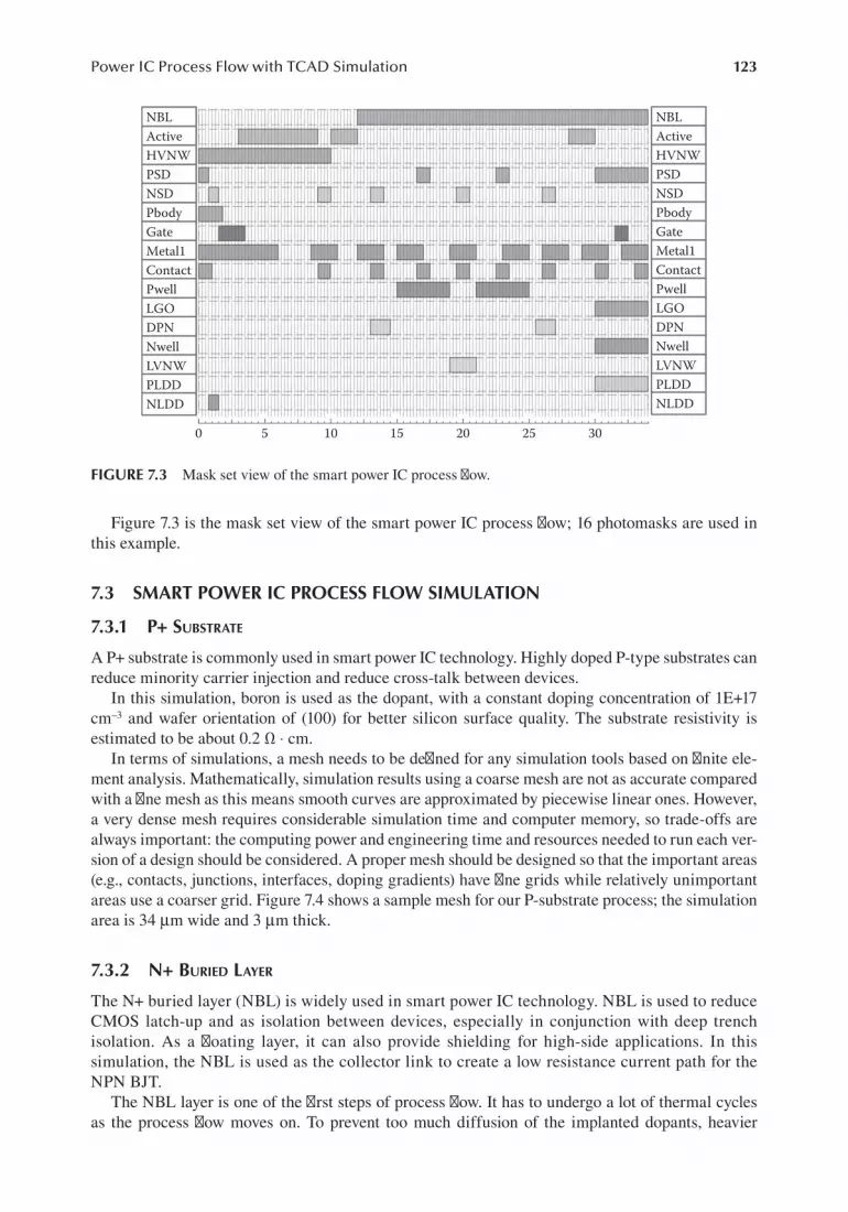
123Power IC Process Flow with TCAD Simulation
Figure 7.3 is the mask set view of the smart power IC process flow; 16 photomasks are used in this example.
7.3 SMART POWER IC PROCESS FLOW SIMULATION
7.3.1 p+ suBstrAte
A P+ substrate is commonly used in smart power IC technology. Highly doped P-type substrates can reduce minority carrier injection and reduce cross-talk between devices.
In this simulation, boron is used as the dopant, with a constant doping concentration of 1E+17 cm–3 and wafer orientation of (100) for better silicon surface quality. The substrate resistivity is estimated to be about 0.2 Ω ⋅ cm.
In terms of simulations, a mesh needs to be defined for any simulation tools based on finite ele-ment analysis. Mathematically, simulation results using a coarse mesh are not as accurate compared with a fine mesh as this means smooth curves are approximated by piecewise linear ones. However, a very dense mesh requires considerable simulation time and computer memory, so trade-offs are always important: the computing power and engineering time and resources needed to run each ver-sion of a design should be considered. A proper mesh should be designed so that the important areas (e.g., contacts, junctions, interfaces, doping gradients) have fine grids while relatively unimportant areas use a coarser grid. Figure 7.4 shows a sample mesh for our P-substrate process; the simulation area is 34 µm wide and 3 µm thick.
7.3.2 n+ Buried lAyer
The N+ buried layer (NBL) is widely used in smart power IC technology. NBL is used to reduce CMOS latch-up and as isolation between devices, especially in conjunction with deep trench isolation. As a floating layer, it can also provide shielding for high-side applications. In this simulation, the NBL is used as the collector link to create a low resistance current path for the NPN BJT.
The NBL layer is one of the first steps of process flow. It has to undergo a lot of thermal cycles as the process flow moves on. To prevent too much diffusion of the implanted dopants, heavier
NLDD
0 5 10 15 20 25 30
PLDD
NwellDPNLGOPwellContactMetal1GatePbodyNSDPSD
NBLActiveHVNW
LVNW
NLDDPLDD
NwellDPNLGOPwellContactMetal1GatePbodyNSDPSD
NBLActiveHVNW
LVNW
FIGURE 7.3 Mask set view of the smart power IC process flow.

124 Integrated Power Devices and TCAD Simulation
species with lower diffusion coefficients like arsenic (As) and antimony (Sb) are used instead of phosphorus; a screen oxide is also used to keep contaminants away and reduce channeling effects. Channeling allows dopants to travel deeper before colliding with lattice atoms and is an unwanted feature of ion implantation. A photomask is used to define the area for the NBL implant. In this simulation, NBL is used only for NPN BJT and PMOS: as shown in Figure 7.5, the NBL implant in the silicon portion where LDMOS is to be built will be blocked by a photoresist layer 1 µm thick.
In this simulation, screen oxide is thermally grown in H2O to achieve a thickness of 200 Å. The growth condition is 15 minutes at 1000°C. Arsenic is used as the dopant and implanted with energy of 15 keV and a dose of 1E+14 cm–2; note that in real fabrication, a much higher dose (1E+15 cm–2 or above) is commonly used for NBL. After implant, implant damage anneal and drive-in are carried out. In the simulation, the furnace has an initial temperature of 800°C and is ramped up to 1000°C over 10 minutes. The temperature is then kept at 1000°C for 20 minutes before being ramped down to 800°C for another 10 minutes. The process recipe is listed in Table 7.1 and the temperature vs. time curve is plotted in Figure 7.6; the ramp rate in this process step is 20°C/min. In future simula-tion steps, we may ignore the temperature ramping and just use constant furnace temperature at plateau for simplicity. Please note that the NBL layer will diffuse upward with later thermal cycles such as those for the epi layer and high-voltage wells.
The process simulation result of NBL is illustrated in Figure 7.7. Subsequent process steps will further drive the NBL implant in all directions.
7.3.3 epitAxiAl lAyer growtH And deep n link
An epitaxial layer (or epi layer) of silicon is grown in a special furnace after the NBL implantation: the crystal orientation of that layer will follow that of the substrate material. In fabrication a (100)
33323130
SiSiO2PhRs
Material Number
Silicon
Photoresist
29282726252423222120191817161514131211109876543210
2.5
1.5
0.5
–0.50
1
–1
2
FIGURE 7.5 Photomask for NBL implant.
33323130
SiMaterial Number
Silicon
29282726252423222120191817161514131211109876543210
2.5
1.5
0.50
1
2
FIGURE 7.4 P-substrate simulation result with mesh plot.

125Power IC Process Flow with TCAD Simulation
Si surface is often used to produce a high-quality epitaxial layer with low defect density. In situ doping is necessary to control the epi layer resistivity.
In the simulation, the vertical grid lines will be inherited from the substrate grid, while hori-zontal grid lines need to be defined for all deposited/grown layers. For simulation purpose, we can simply use the deposition of silicon with constant P-type (boron) doping instead of real silicon epi growth. The thermal budget of the epi layer growth is combined with the previous NBL drive-in step and the deep N-link (DPN) step that follows the epi layer growth.
In this mock-up process flow, we break up the epitaxial growth into two steps. After each growth step, a photomask is used to create deep N-type implanted wells that connect the silicon surface to the NBL layer. These deep N-links are used for NPN BJTs in this simulation. The first epitaxial layer has a thickness of 3 µm, and the second epi layer is thinner with a thickness of 2 µm for a total
30 40100800°C
1000°C
Tem
pera
ture
(°C
)
Plateau
20°C/min
Time (minutes)
20°C/min
FIGURE 7.6 Furnace anneal with temperature ramp up and down.
TABLE 7.1Diffuse Parameters for NBL Anneal and Drive-in
Process Name Time (minutes) Initial Temperature (°C) Final Temperature (°C) Condition
Diffuse 10 800 1000 Nitrogen
Diffuse 20 1000 1000 Nitrogen
Diffuse 10 1000 800 Nitrogen
33–20
+X
–15–10–505101520
Net_Doping
323130
NBL
P-Substrate
29282726252423222120191817161514131211109876543210
2.53
1.5
0.50
1
2
FIGURE 7.7 Net doping plot after NBL anneal.

126 Integrated Power Devices and TCAD Simulation
epi layer thickness of 5 µm. The epi layer is in situ doped with boron to create a constant doping of 1E+16 cm–3. The process parameters are listed in Table 7.2. Note that epi layer growth is a thermal process, but in simulation we simply deposit silicon on top of the substrate. In real processes, the epi growth temperature should be designed so that the associated thermal budget is negligible.
The reason that we do not grow the epi layer in one step is because of the DPN implants. A very deep implant greater than a few microns is difficult to realize, and typically very high implant energy levels need to be applied. High energy combined with high dose implants will substantially damage the silicon lattice, which causes undesirable transient enhanced diffusion effects. Even though in practice implant energies can be in the MeV range, we will use maximum implant energy of 900 keV in this simulation.
An implant chain (combining several individual ion implants into a single process step) is neces-sary to create a smooth and deep implant after drive-in. For the first DPN implant, we use the implant conditions listed in Table 7.3, the photomask step for DPN implant is simulated in Figure 7.8.
TABLE 7.2Epi Layer Process Simulation Parameters
Process Name Material Thickness (µm) DopantsDoping
Concentration (cm–3)
Deposit Silicon 3 Boron 1E+16
Deposit Silicon 2 Boron 1E+16
TABLE 7.3Implant Chain Parameters of the First DPN Implant
Process Name Dopants Energy (keV) Dose (cm–2) Angle (°) Rotation (°)
Implant Phosphorus 100 3E+12 0 0
Implant Phosphorus 375 3E+12 0 0
Implant Phosphorus 675 3E+12 0 0
Implant Phosphorus 900 3E+12 0 0
33323130
SiPhRs
Material Number
Silicon
Photoresist Photoresist Photoresist
29282726252423222120191817161514131211109876543210
2.51.5
10.5
–0.50
–1–1.5–2.5–3.5
–4–4.5
–5–5.5
–2–3
2
FIGURE 7.8 Photomask for DPN implant.

127Power IC Process Flow with TCAD Simulation
Since the second epitaxial layer is thinner (2 µm) than the first one (3 µm), we can use lower implant energies; the implant chain parameters are listed in Table 7.4.
A thermal process is necessary to anneal implant damage as well as activate and drive-in the dop-ants in DPN; the process simulation parameters for this step is listed in Table 7.5. This is a high ther-mal budget drive-in step to allow both the DPN and NBL layers diffuse to the desired depth and width.
The net doping plot after the DPN anneal/drive-in is illustrated in Figure 7.9.
7.3.4 HigH-voltAge twin-well
High-voltage twin-well consists of a high-voltage N-well (HVNW) and a high-voltage P-well (HVPW). They are used to create the drift regions for n-LDMOS and p-LDMOS. For process simu-lation in this chapter, only n-LDMOS is included so only HVNW is simulated.
HVNW is a relatively lightly doped N-well (about 1E+16 cm–3) since it has to support high breakdown voltages. The depth of the well is about 1.5 µm in this simulation. Like the deep N-link, an implant chain must be used to make the well deeper and more uniform. A large thermal cycle is also necessary to allow dopant diffusion, which will also apply to the previously implanted wells (NBL and DPN). Thermal cycles in later process steps will create even further diffusion of the already implanted wells, which is why implant wells that require large thermal budgets are always
TABLE 7.5Diffuse Parameters for Second DPN Anneal and Drive-in
Process Name Time (minutes) Initial Temperature (°C) Final Temperature (°C) Condition
Diffuse 80 1100 1100 Nitrogen
TABLE 7.4Implant Chain Parameters of Second DPN Implant
Process Name Dopants Energy (keV) Dose (cm–2) Angle (°) Rotation (°)
Implant Phosphorus 150 2E+12 0 0
Implant Phosphorus 400 1E+12 0 0
Implant Phosphorus 550 1E+12 0 0
Implant Phosphorus 700 5E+12 0 0
33 34 +X
Net_Doping18.6925
15
10
5
–5
–10
–15
–17
0
323130
P-epiNBL
P-Substrate
DPN DPN
29282726252423222120191817161514131211109876543210
2.53
1.51
0.5–0.5
0–1
–1.5–2.5–3.5
–4–4.5
–2–3
2
FIGURE 7.9 Net doping plot after DPN implant anneal and drive-in.

128 Integrated Power Devices and TCAD Simulation
processed first. Well implants that need smaller thermal budgets to prevent dopants from diffusing too much (e.g., source/drain implants) are usually placed at the very end of the process flow.
In real fabrication, a thin layer of sacrificial oxide is usually used to protect the silicon surface from direct implant damage and contaminants and to prevent dopants from escaping the silicon during annealing. For shallow implant, this thin oxide layer can help reduce the channeling effect, which causes implanted dopants to travel too deep in the silicon lattice.
In this simulation, a thin layer of oxide is deposited, but we will not repeat this step for the rest of this chapter for the sake of simplicity. The simulation parameters are listed in Table 7.6, Table 7.7, and Table 7.8. The photomask for HVNW is shown in Figure 7.10.
The process simulation result after implant drive-in is illustrated in Figure 7.11. We see that after the thermal process of HVNW the deep N-link is now connected to the NBL.
7.3.5 p-Body implAnt For n-ldmos
This process step is dedicated to create a P-type implant well for the body region of the n-LDMOS. The photomask for the P-body implant is shown in Figure 7.12.
This well must be deep enough to be useful, and setting the doping concentration can be quite tricky. If the doping level is too low, it may cause punch-through of the depletion region from the drain-drift/P-body junction to the source/P-body junction, and leakage current surge can cause premature breakdown. Also, a lightly doped P-region will increase base resistance of the parasitic NPN BJT of the LDMOS. As we shall see in Chapter 8, higher base resistance will increase the risk of turning on the parasitic BJT, which eventually causes permanent damage to the LDMOS. On the other hand, a heavily doped P-body is not feasible either, since it will greatly increase the threshold voltage and create a longer channel by diffusion. Table 7.9 lists the process condition for P-body implant; boron is used as the dopant.
TABLE 7.7HVNW Implant Process Simulation Parameters
Process Name Dopants Energy (keV) Dose (cm–2) Angle (°) Rotation (°)
Implant Phosphorus 150 1E+12 0 0
Implant Phosphorus 350 1E+12 0 0
Implant Phosphorus 550 1E+12 0 0
Implant Phosphorus 750 1E+12 0 0
TABLE 7.8HVNW Iimplant Drive-in Simulation Parameters
Process Name Time (minutes) Initial Temperature (°C) Final Temperature (°C) Condition
Diffuse 120 1100 1100 Nitrogen
TABLE 7.6HVNW Pad Oxide Simulation Parameters
Process Name Material Thickness (µm)
Deposit Oxide 0.01

129Power IC Process Flow with TCAD Simulation
33323130
Photoresist
Silicon
29
Material Number
PhRsSi
282726252423222120191817161514131211109876543210
2.51.5
10.5
–0.50
–1–1.5–2.5–3.5
–4–4.5–5.5
–5
–2–3
2
FIGURE 7.12 Photomask of P-body implant.
33323130
Photoresist
Silicon
29
Material NumberPhRsSiO2Si
282726252423222120191817161514131211109876543210
2.51.5
10.5
–0.50
–1–1.5–2.5–3.5
–4–4.5
–5.5–5–6
–2–3
2
FIGURE 7.10 Photomask for HVNW.
33 34 +X
Net_Doping18.5536
15
10
5
–5
–10
–15
–17
0
323130
P-epiNBL
P-Substrate
DPNHVNW
DPN
29282726252423222120191817161514131211109876543210
2.53
1.51
0.5–0.5
0–1
–1.5–2.5–3.5
–4–4.5
–2–3
2
FIGURE 7.11 Net doping after HVNW drive-in.
TABLE 7.9P-Body Implant Process Simulation Parameters
Process Name Dopants Energy (keV) Dose (cm–2) Angle (°) Rotation (°)
Implant Boron 100 5E+13 0 0

130 Integrated Power Devices and TCAD Simulation
After implant, an anneal step is necessary to activate the dopants and drive-in the implanted well to the desired depth and width. The doping concentration of the well is related to the total thermal budget: engineers should use the total thermal budget after a particular well implant to estimate how much diffusion occurs and how high the doping concentration is at the end of the process. TCAD software provides a useful calculation in this regard. Table 7.10 gives the simulation drive-in time and temperature after P-body implant. Note that photoresist needs to be removed before any diffu-sion step.
The process simulation result after P-body anneal is shown in Figure 7.13.
7.3.6 Active AreA/sHAllow trencH isolAtion (sti)
The phrase active area describes regions that perform “active” functions. Basically it means the areas used to build devices and are not used for isolation. However, in power devices like LDMOS, oxide layers can also be used within the device to improve breakdown voltage. In GDSII files, active areas are drawn with oxide layer covered areas defined.
Shallow trench isolation (STI) is an isolation technology used widely in today’s CMOS, BiCMOS, and BCD fabrications. In the past, LOCOS (LOCal Oxidation of Silicon) was the mainstream technol-ogy, but as devices shrink and enter the submicron regime, LOCOS (with its bird’s beak shaped oxide) takes up too much silicon real estate. It also causes an uneven Si surface that is undesirable for photoli-thography. Most of today’s process technology with feature size smaller than 0.25 µm use STI instead of LOCOS because of its advantages of compactness and smooth surface for lithography. In this chap-ter, only STI will be discussed. Interested readers can read classic books [135] by Drs. Plummer, Deal, and Griffin from Stanford University for a detailed explanation of LOCOS technology.
The STI process simulation starts with pad oxide and nitride deposition. Si3N4 (nitride) is used as an etch stop layer for chemical mechanical polishing (CMP) while the pad oxide is used to release the stress that is introduced by the nitride layer. The pad oxide is thermally grown to 400 Å by wet oxidation. The nitride is deposited and has a thickness of 800 Å. The process simulation parameters for the pad oxide and the nitride layer are listed in Tables 7.11 and 7.12.
TABLE 7.10P-Body Implant Drive-in Simulation Parameters
Process Name Time (minutes) Initial Temperature (°C) Final Temperature (°C) Condition
Diffuse 30 1000 1000 Nitrogen
33 34 +X
Net_Doping20
15
10
5
–5
–10
–15
–20
0
323130
P-epiNBL
P-Substrate
DPNHVNW
Pbody
DPN
292827262524232221201918171615141312111098765432102.5
3
1.51
0.5–0.5
0–1
–1.5–2.5–3.5
–4–4.5
–2–3
2
FIGURE 7.13 Net doping plot after P-body implant anneal.

131Power IC Process Flow with TCAD Simulation
The process simulation result after pad oxide and nitride deposit is shown in Figure 7.14, with a zoom-in view of the top 0.6 µm.
The next step is to etch a shallow trench. In fabrication, photolithography steps using masks for active/STI are used to expose and develop the photoresist and define areas to be covered or to be exposed. Reactive ion etching (RIE) is typically applied to remove the nitride layer and pad oxide and gain access to the silicon in the exposed area. The silicon is then dry-etched to a certain depth to create trenches with very small angles in the sidewalls. In simulation, the depth of the silicon etch is chosen to be 0.3 µm, and sidewall angle is 2 degrees, measured from the plane normal to silicon surface. The process simulation parameters for the STI etching are listed in Table 7.13. Some overetch of nitride and oxide is necessary to make sure they are completely removed from the areas where they are not needed.
Figure 7.15 is the process simulation result after the STI etch.Before we fill in the etched trench, a dry liner oxide is thermally grown. This liner is important
for the STI/silicon interface quality since dry oxide is denser and usually has a more superior qual-ity than deposited oxide. The oxide/silicon interface quality will impact device reliability like hot carrier injection (HCI) for power LDMOS. Table 7.14 illustrates the process simulation parameters for STI liner oxide growth. The process simulation result after the STI liner is shown in Figure 7.16, and an enlarged view of the STI liner is given in Figure 7.17.
TABLE 7.11Process Simulation Parameters for STI Pad Oxide Growth
Process Name Time (minutes) Initial Temperature (°C) Final Temperature (°C) Condition
Diffuse 15 900 900 Wet oxide
TABLE 7.12Process Simulation Parameters for STI Nitride Layer
Process Name Material Thickness (µm)
Deposit Nitride 0.08
Oxide
Nitride
Silicon
Material Number
SiNiSiO2Si
0
–4.55–4.5
–4.6–4.65
–4.75
–4.85–4.9
–4.95
–5.05–5
–4.7
–4.8
323028262422201816141210987654321
FIGURE 7.14 Process simulation result after pad oxide growth and nitride deposition.

132 Integrated Power Devices and TCAD Simulation
TABLE 7.13Process Simulation Parameters for STI Etch Steps
Process Name Material Thickness (µm) Angle (°) Etch Condition
Etch Nitride 0.1 2 Dry
Etch Oxide 0.05 2 Dry
Etch Silicon 0.3 2 Dry
33323130
Photoresist
Silicon
STI EtchNitride
29
Material NumberSiSiO2SiNi
2827262524232221201918171615141312111098765432102.51.5
10.5
–0.50
–1–1.5–2.5–3.5
–4–4.5
–5
–2–3
2
FIGURE 7.15 Process simulation result after STI etch.
TABLE 7.14Process Simulation Parameters for STI Oxide Liner Growth
Process Name Time (minutes) Initial Temperature (°C) Final Temperature (°C) Condition
Diffuse 10 1000 1000 Dry oxide
33323130
Photoresist
Silicon
STI Liner
Nitride
STI Liner
29
Material NumberSiSiO2SiNi
2827262524232221201918171615141312111098765432102.51.5
10.5
–0.50
–1–1.5–2.5–3.5
–4–4.5
–5
–2–3
2
FIGURE 7.16 Process simulation result after STI liner growth.

133Power IC Process Flow with TCAD Simulation
With the oxide liner complete, we are ready to fill the trench with deposited oxide. In fabrication, high-density plasma (HDP) oxide is deposited using chemical vapor deposition (CVD). In simula-tion, oxide is deposited with a layer thickness of 0.5 µm. The process simulation parameters are listed in Table 7.15. Figure 7.18 shows the process simulation result after the oxide fill step.
CMP is performed to get rid of extra oxide and nitride to leave a flat surface. In fabrica-tion, CMP typically stops at a certain designed nitride thickness; the remaining nitride is then stripped off using the hot phosphor method. In simulation, a square etch with designated x1, x2,
TABLE 7.15Process Simulation Parameters for STI Oxide Fill
Process Name Material Thickness (µm)
Deposit Oxide 0.5
12.512.251211.7511.511.251110.7510.510.25109.759.5
Nitride Nitride
Oxide Oxide
Material NumberSiSiO2SiNi–4.5
–4.9–4.85
–4.8–4.75
–4.7–4.65
–4.6–4.55
–4.95–5
–5.05
Oxide Liner
Silicon
FIGURE 7.17 Enlarged view of oxide liner with Y from –4.5 µm to –5.1 µm and X from 9.5 µm to 12.5 µm.
33323130
Silicon
Oxide Oxide Oxide
Nitride
29
Material NumberSiSiO2SiNi
2827262524232221201918171615141312111098765432102.51.5
10.5
–0.50
–1–1.5–2.5–3.5
–4–4.5
–5–5.5
–2–3
2
FIGURE 7.18 Process simulation result after oxide fill step.

134 Integrated Power Devices and TCAD Simulation
y1, and y2 coordinates is applied to get rid of all materials within the specified area. Table 7.16 is the process simulation parameters for the square etch. Please note that in the process simu-lator the positive direction for the Y axis points downward toward the substrate. So the mesh points with y = –20 µm are above those with y = –4.95 µm. Figure 7.19 shows how the four coordinates are arranged in the process simulation. After square etch, the remaining nitride is removed. Figure 7.20 shows the simulation result after CMP and nitride removal.
7.3.7 n-well And p-well
N-well and P-well twin wells implant have relatively higher doping concentration. N-well is used for digital PMOS, whereas P-well is used as the base region of the NPN BJT. The process simulation parameters for N-well and P-well are listed in Tables 7.17 and 7.18.
Figure 7.21 shows the photomask of N-well while the photomask of P-well is shown in Figure 7.22.
TABLE 7.16Process Simulation Parameters for Square Etch
Process Name Material (X1,Y1) (µm) (X2,Y2) (µm)
Square etch All (0, –20) (34, –4.95)
(x2, y2)
(x2, y1)
(x1, y2)
(x1, y1)
FIGURE 7.19 The four coordinates in a square etch simulation.
33323130
Silicon
Oxide Oxide Oxide
29
Material NumberSiSiO2
282726252423222120191817161514131211109876543210
2.51.5
10.5
–0.50
–1–1.5–2.5–3.5
–4–4.5
–2–3
2
FIGURE 7.20 Process simulation for STI formation after CMP and nitride removal.

135Power IC Process Flow with TCAD Simulation
TABLE 7.17Process Simulation Parameters for N-Well Implant
Process Name Dopants Energy (keV) Dose (cm–2) Angle (°) Rotation (°)
Implant Phosphorus 50 1E+13 0 0
TABLE 7.18Process Simulation Parameters for P-Well Implant
Process Name Dopants Energy (keV) Dose (cm–2) Angle (°) Rotation (°)
Implant Boron 30 1E+13 0 0
33323130
Silicon
PhotoresistOxide Oxide Oxide
29
Material Number
SiPhRs
SiO2
282726252423222120191817161514131211109876543210
2.51.5
10.5
–0.50
–1–1.5–2.5–3.5
–4–4.5
–5–5.5
–2–3
2
FIGURE 7.21 Photomask of N-well.
33323130
Silicon
PhotoresistOxide Oxide Oxide
29
Material Number
SiPhRs
SiO2
282726252423222120191817161514131211109876543210
2.51.5
10.5
–0.50
–1–1.5–2.5–3.5
–4–4.5
–5–5.5
–2–3
2
FIGURE 7.22 Photomask of P-well.

136 Integrated Power Devices and TCAD Simulation
After implant, a thermal process is performed to activate the dopants and drive-in the wells. The process simulation parameters for N-well and P-well drive-in are listed in Table 7.19. Figure 7.23 is the net doping plot after N-well and P-well drive-in.
7.3.8 low-voltAge twin wells
Low-voltage N-well (LVNW) and low-voltage P-well (LVPW) are highly doped wells in the process flow. In our example, LVNW is used as the highly doped emitter region of the NPN BJT. The pho-tomask of LVNW is shown in Figure 7.24.
The ion implantation process simulation parameters for LVNW are listed in Table 7.20. The thermal anneal and drive-in simulation parameters are listed in Table 7.21.
The process simulation result after LVNW implant anneals and drive-in is shown in Figure 7.25.
TABLE 7.19Process Simulation Parameters for N-Well and P-Well Drive-in
Process Name Time (minutes) Initial Temperature (°C) Final Temperature (°C) Condition
Diffuse 10 900 1000 Nitrogen
Diffuse 20 1000 1000 Nitrogen
Diffuse 10 1000 900 Nitrogen
33 34 +X
Net_Doping20
15
10
5
–5
–10
–15
–20
0
323130
P-epiNBL
P-Substrate
DPNHVNW
Pbody P-well P-wellSTI STISTI
DPN N-well
292827262524232221201918171615141312111098765432102.5
3
1.51
0.5–0.5
0–1
–1.5–2.5–3.5
–4–4.5
–2–3
2
FIGURE 7.23 Net doping plot after N-well and P-well drive-in.
33323130
Silicon
PhotoresistOxide Oxide Oxide
29
Material Number
SiO2
PhRs
Si
282726252423222120191817161514131211109876543210
2.51.5
10.5
–0.50
–1–1.5–2.5–3.5
–4–4.5
–5–5.5
–2–3
2
FIGURE 7.24 Photomask for LVNW.

137Power IC Process Flow with TCAD Simulation
7.3.9 tHick gAte And tHin gAte oxide
Unlike a CMOS process flow, there are multiple gate oxide thicknesses for smart power ICs. In our example, two gate oxide thicknesses are chosen: a thick gate oxide for power devices like LDMOS; and a thin gate oxide for digital/analog MOSFETs.
The thick gate oxide (240 Å) is grown first. There is no photomask used for this step, and it is grown everywhere on the wafer. The process simulation parameters for the thick gate oxide growth are listed in Table 7.22, and the process simulation results are illustrated in Figure 7.26. For digital and analog MOSFETs, a thinner gate oxide is required; otherwise the threshold voltage will be too high. Our previous step has grown a thick gate oxide everywhere on the wafer active area, so a photomask is now used to expose the locations where a thinner gate oxide is needed. Figure 7.27 is the process simulation view of a thin gate oxide photomask.
TABLE 7.20Process Simulation Parameters for LVNW Implant
Process Name Dopants Energy (keV) Dose (cm–2) Angle (°) Rotation (°)
Implant Phosphorus 20 5E+14 0 0
TABLE 7.21Process Simulation Parameters for LVNW Anneal and Drive-in
Process Name Time (minutes) Initial Temperature (°C) Final Temperature (°C) Condition
Diffuse 10 900 1000 Nitrogen
TABLE 7.22Process Simulation Parameters for Thick Gate Oxide Growth
Process Name Time (minutes) Initial Temperature (°C) Final Temperature (°C) Condition
Diffuse 20 1000 1000 Dry oxide
33 34 +X
Net_Doping20
15
10
5
–5
–10
–15
–20
0
323130
P-epiNBL
P-Substrate
DPNHVNW
Pbody P-well P-wellSTI STISTI
DPN N-wellLVNW
292827262524232221201918171615141312111098765432102.5
3
1.51
0.5–0.5
0–1
–1.5–2.5–3.5
–4–4.5
–2–3
2
FIGURE 7.25 Net doping after LVNW implant anneal and drive-in.

138 Integrated Power Devices and TCAD Simulation
33323130
Silicon
PhotoresistOxide Oxide Oxide
29
Material Number
SiO2
PhRs
Si
282726252423222120191817161514131211109876543210
2.51.5
10.5
–0.50
–1–1.5–2.5–3.5
–4–4.5
–5–5.5
–2–3
2
FIGURE 7.27 Photomask of thin gate oxide.
TABLE 7.23Dry Etch for Thin Gate Oxide Growth
Process Name Material Thickness (µm) Angle (°) Etch Condition
Etch Oxide 0.03 0 Dry
33323130
Oxide Oxide Oxide
29
Material Number
Area exposed for thin Gate Oxide (GOX)
SiSiO2
282726252423222120191817161514131211109876543210–4
–4.5
–4.75
–4.25
FIGURE 7.28 Enlarged view of the oxide etched region.
3332
SiO2Si
3130
Oxide Oxide Oxide
Gate oxide all over the wafer after ick GateOxide (TGO) growth
292827
Material Number
26252423222120191817161514131211109876543210–2
–2.5–2.25
–2.75
–3.25
–3.75
–4.5–4.25
–4
–4.75
–3
–3.5
FIGURE 7.26 Process simulation result of thick gate oxide growth (enlarged view).

139Power IC Process Flow with TCAD Simulation
In our example, only the PMOS area is exposed by the photomask. The thick gate oxide in the exposed area is subsequently etched with simulation parameters listed in Table 7.23. An enlarged view of the oxide etched portion after etching the thick gate oxide is shown in Figure 7.28.
A second oxidation process is performed to grow thin gate oxide; like our previous step, the thin gate oxide is grown throughout the wafer. The area where the thick gate oxide was etched away has a higher growth rate than those areas still covered by the thicker gate oxide. Table 7.24 lists the process condition for thin gate oxide growth. The final thin gate oxide thickness is about 34 Å, and thick gate oxide is about 250 Å. The process simulation result after thin oxide growth is shown in Figure 7.29, and an enlarged view is provided in Figure 7.30.
3332
SiO2Si
3130
ick Gate Oxide (TGO)
Silicon
in Gate Oxide (GOX)
292827
Material Number
26252423222120191817161514131211109876543210
–2.5–2
–2
–3
–4.5–4
–3.5
Oxide Oxide Oxide
–0.5–1.5
–1–1.5
0
–2.5
FIGURE 7.29 Process simulation result after thin oxide growth.
TABLE 7.24Process Simulation Parameters for Thin Gate Oxide Growth
Process Name Time (minutes) Initial Temperature (°C) Final Temperature (°C) Condition
Diffuse 5 900 900 Dry oxide
27.5 28 28.5 29 29.5 30 30.5 31
TGO Oxide COX Oxide
ick GateOxide (TGO)
in GateOxide (GOX)
Oxide
Material Number
SiSiO2
–4.85
–4.8
–4.75
–4.7
–4.65
–4.6
–4.9
–4.95
Silicon
FIGURE 7.30 Process simulation result after thin oxide growth with enlarged view: x from 27 µm to 31 µm and y from –4.6 µm to –5 µm.

140 Integrated Power Devices and TCAD Simulation
7.3.10 poly gAte
Multiple polysilicon (poly) layers are normally used in smart power IC process flow to create, for example, poly-insulator-poly capacitors. In this example, only one poly layer is simulated. The poly layer in the simulation has a thickness of 0.25 µm (2500 Å) and is in situ doped with phosphorus. The process parameters for poly deposition are listed in Table 7.25.
After poly deposition, a dry etch is performed and the exposed poly is etched away while the material underneath the photomask is preserved. A thermal step is necessary to activate the dopants in the poly and the process simulation parameters are listed in Table 7.26. In comparison with previ-ous thermal steps, poly anneal has a smaller thermal budget to mimic the widely adopted practice of rapid thermal anneal (RTA).
The finished polysilicon gate simulation is shown in Figure 7.31. Both the LDMOS gate and PMOS gate are created at the same time. An enlarged view (Figure 7.32) of the LDMOS gate corner indicates there is a step-coverage at the STI/silicon boundary. In real fabrication (not in simulation), this corner may have a large impact on device reliability if the corner somehow leads to a thinner gate oxide [179].
TABLE 7.25Process Simulation Parameters for Poly Deposition
Process Name Material Thickness (µm) Dopants Doping Concentration (cm–3)
Deposit Poly 0.25 Phosphorus 1E+20
TABLE 7.26Process Simulation Parameters for Poly Thermal Anneal
Process Name Time (minutes) Initial Temperature (°C) Final Temperature (°C) Condition
Diffuse 1 850 1000 Nitrogen
Diffuse 1 1000 1000 Nitrogen
Diffuse 1 1000 850 Nitrogen
33323130
Silicon
OxidePoly Oxide Oxide
in Gate Oxide (GOX)ick Gate Oxide (TGO)
29
Material Number
Si
PolySiO2
282726252423222120191817161514131211109876543210
2.51.5
10.5
–0.50
–1–1.5–2.5–3.5
–4–4.5
–5
–2–3
2
Poly
FIGURE 7.31 Process simulation result of poly gates.

141Power IC Process Flow with TCAD Simulation
2.1 2.2 2.3 2.4 2.5 2.6 2.7 2.8 2.9 3 3.1 3.2 3.3 3.4 3.5 3.6 3.7 3.8 3.9 42 4.1
Poly
Nitride
ick Gate Oxidein Gate
Oxide (GOX)
STI Material Number
Si
PolySiO2
–5
–4.9
–4.8
–4.7
–4.6
–4.5
–5.1
–5.2
Silicon
FIGURE 7.32 An enlarged view of LDMOS poly gate at STI corner.
33323130
Silicon
PhotoresistOxide
Poly Oxide Oxide
29
Material Number
Si
PolyPhRs
SiO2
282726252423222120191817161514131211109876543210
2.51.5
10.5
–0.50
–1–1.5–2.5–3.5
–4–4.5
–5–5.5
–6
–2–3
2
Poly
FIGURE 7.33 Photomask for NLDD implant.
33323130
Silicon
PhotoresistOxide
PolyOxide Oxide
29
Material Number
Si
SiO2PhRs
Poly
282726252423222120191817161514131211109876543210
2.51.5
10.5
–0.50
–1–1.5–2.5–3.5
–4–4.5
–5–5.5
–6
–2–3
2
Poly
FIGURE 7.34 Photomask for PLDD implant.

142 Integrated Power Devices and TCAD Simulation
7.3.11 nldd And pldd
NLDD (or PLDD) stands for N (or P) type lightly doped drain. The lightly doped drain implant is primarily used to alleviate the high electric field near the heavily doped drain. Since for digital MOSFETs source and drain are interchangeable, this implant applies to both drain and source. The photomasks for NLDD and PLDD are shown in Figures 7.33 and 7.34, respectively.
Similar to a CMOS process flow, NLDD and PLDD are implanted after the gate poly is defined: the gate serves as an implant block for the low energy implant of the LDD, and the implanted wells are self-aligned to the gates. In this simulation, NLDD is used for n-LDMOS, and PLDD is used for PMOS. The NLDD and PLDD process simulation parameters are listed from Tables 7.27 to 7.30.
For NLDD, phosphorus or arsenic can be used, whereas for PLDD BF2 is normally used instead of boron because the heavier ion will create a shallower implant that is desirable for this step. A quick anneal is performed to activate the dopants, with a much smaller thermal budget than the one used for previous well implants where we deliberately use a long thermal cycle to allow dopants to diffuse and form a DPN or P-well. This is because like in a CMOS process, LDD needs little dif-fusion to create a shallow junction and minimize the short channel effect; in real manufacturing,
TABLE 7.27Process Simulation Parameters for NLDD Implant
Process Name Dopants Energy (keV) Dose (cm–2) Angle (°) Rotation (°)
Implant phosphorus 20 9E+12 0 0
TABLE 7.29Process Simulation Parameters for PLDD Implant
Process Name Dopants Energy (keV) Dose (cm–2) Angle (°) Rotation (°)
Implant BF2 40 2E+13 0 0
TABLE 7.30Process Simulation Parameters for PLDD Thermal Anneal
Process Name Time (seconds) Initial Temperature (°C) Final Temperature (°C) Condition
Diffuse 30 seconds 1000 1000 Nitrogen
TABLE 7.28Process Simulation Parameters for NLDD Thermal Anneal
Process Name Time (seconds) Initial Temperature (°C) Final Temperature (°C) Condition
Diffuse 20 seconds 1000 1000 Nitrogen
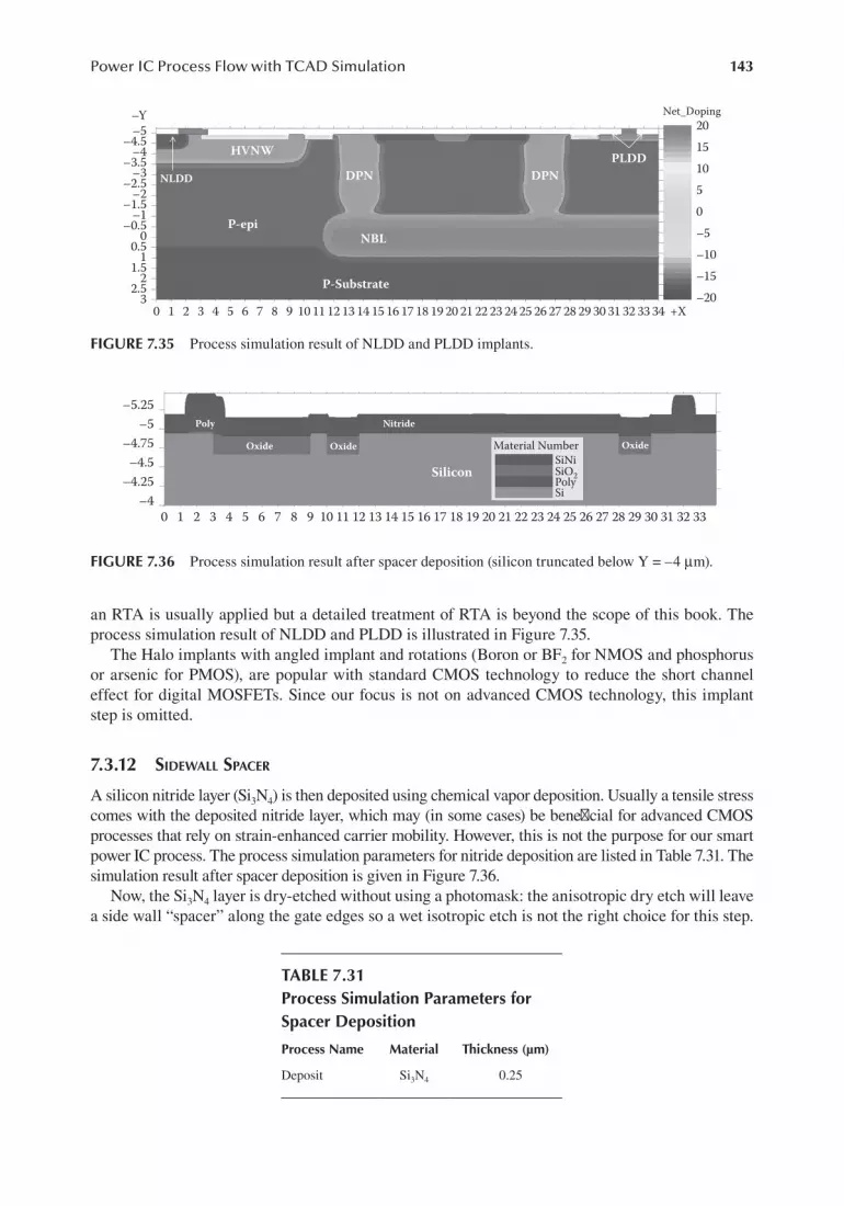
143Power IC Process Flow with TCAD Simulation
an RTA is usually applied but a detailed treatment of RTA is beyond the scope of this book. The process simulation result of NLDD and PLDD is illustrated in Figure 7.35.
The Halo implants with angled implant and rotations (Boron or BF2 for NMOS and phosphorus or arsenic for PMOS), are popular with standard CMOS technology to reduce the short channel effect for digital MOSFETs. Since our focus is not on advanced CMOS technology, this implant step is omitted.
7.3.12 sidewAll spAcer
A silicon nitride layer (Si3N4) is then deposited using chemical vapor deposition. Usually a tensile stress comes with the deposited nitride layer, which may (in some cases) be beneficial for advanced CMOS processes that rely on strain-enhanced carrier mobility. However, this is not the purpose for our smart power IC process. The process simulation parameters for nitride deposition are listed in Table 7.31. The simulation result after spacer deposition is given in Figure 7.36.
Now, the Si3N4 layer is dry-etched without using a photomask: the anisotropic dry etch will leave a side wall “spacer” along the gate edges so a wet isotropic etch is not the right choice for this step.
33 34 +X
2015105
–5–10–15–20
0
323130
P-epiNBL
P-Substrate
HVNW
DPN DPNPLDD
NLDD
29
Net_Doping
282726252423222120191817161514131211109876543210
2.53
1.51
0.5–0.5
0–1
–1.5–2.5–3.5
–4–4.5
–5–Y
–2–3
2
FIGURE 7.35 Process simulation result of NLDD and PLDD implants.
33323130
Oxide
Poly Nitride
Silicon
Oxide Oxide
29
Material Number
SiPoly
SiNiSiO2
282726252423222120191817161514131211109876543210–4
–4.5
–5–4.75
–5.25
–4.25
FIGURE 7.36 Process simulation result after spacer deposition (silicon truncated below Y = –4 µm).
TABLE 7.31Process Simulation Parameters for Spacer Deposition
Process Name Material Thickness (µm)
Deposit Si3N4 0.25

144 Integrated Power Devices and TCAD Simulation
The simulation parameters are listed in Table 7.32. Figure 7.37 is the simulation result after spacer etching, and Figure 7.38 shows an enlarged view with mesh.
7.3.13 nsd And psd
N+ (or P+) source and drain implants (NSD and PSD) are typically one of the last implant steps for smart power IC technology. A shallow junction is required by most modern process technologies for source and drain implant, so these steps use the least amount of thermal budget. NSD is used for n-LDMOS, NPN collector, and emitter contacts. PSD is used for PMOS, NPN base contact, and P-body contact for n-LDMOS. The photomasks for NSD and PSD are shown in Figures 7.39 and 7.40, respectively.
33323130
Silicon
OxidePoly
Oxide Oxide
29
Material Number
Si
SiO2SiNi
Poly
282726252423222120191817161514131211109876543210
2.51.5
10.5
–0.50
–1–1.5–2.5–3.5
–4–4.5
–5
–2–3
2
FIGURE 7.37 Process simulation result after spacer etching.
TABLE 7.32Dry Etch of Nitride Spacer
Process Name Material Thickness (µm) Angle (°) Etch Condition
Etch Si3N4 0.03 0 Dry
2.5 2.6 2.7 2.8 2.9 3.0 3.1 3.2 3.3 3.4 3.5 3.6 3.7 3.8 3.9 +X
Polysilicon
NitrideTGO Gate Oxide
OxideMaterial Number
Nitride Remainig
SiNiPolySiO2
Si
–5–5.05
–4.9–4.95
–4.75–4.8
–4.85
–4.7–4.65
–4.6–4.55
–4.5
–5.1–5.15
–5.2
Silicon
FIGURE 7.38 Process simulation result after spacer etching (enlarged with mesh on).

145Power IC Process Flow with TCAD Simulation
In practice, a pre-amorphization implant step is generally required to reduce the channeling effect and obtain shallower junctions, and an RTA is performed to activate the dopants. The process simulation parameters are listed from Tables 7.33 to 7.36.
The simulation result after NSD and PSD anneal is shown in Figure 7.41. In practice, after the NSD and PSD steps, there should be a self-aligned silicidation process to reduce the contact
33323130
Silicon
PhotoresistOxide
PolyOxide Oxide
29
Material Number
Si
SiO2
SiNiPhRs
Poly
282726252423222120191817161514131211109876543210
2.51.5
10.5
–0.50
–1–1.5–2.5–3.5
–4–4.5
–5–5.5
–6
–2–3
2
FIGURE 7.39 Photomask for NSD implant.
33323130
Silicon
PhotoresistOxide
PolyOxide Oxide
29
Material Number
Si
SiO2
SiNiPhRs
Poly
282726252423222120191817161514131211109876543210
2.51.5
10.5
–0.50
–1–1.5–2.5–3.5
–4–4.5
–5–5.5
–6
–2–3
2
FIGURE 7.40 Photomask for PSD implant.
TABLE 7.33Process Simulation Parameters for NSD Implant
Process Name Dopants Energy (keV) Dose (cm–2) Angle (°) Rotation (°)
Implant Phosphorus 25 1E+14 0 0
TABLE 7.34Process Simulation Parameters for NSD Thermal Anneal
Process Name Time (seconds) Initial Temperature (°C) Final Temperature (°C) Condition
Diffuse 15 seconds 950 950 Nitrogen

146 Integrated Power Devices and TCAD Simulation
resistance. This means a contact metal like cobalt or titanium is deposited and chemical reactions are used to transform the silicon into a silicide. The process simulation for this step is omitted.
7.3.14 BAck-end oF tHe line
Back-end of the line typically refers to the process steps that form interlayer dielectric (ILDs), contacts, vias, and metal layers. In the past, aluminum was used extensively for power IC technol-ogy, but copper is now more prevalent thanks to its lower resistivity and greater immunity to the electromigration problem. However, unlike aluminum, copper is difficult to selectively etch so that deposition and metal patterning methods are not feasible. Fortunately, engineers have developed a new method called dual damascene, which creates etched patterns on the ILD oxides that are then filled in by copper. A CMP step is subsequently performed to expose the copper interconnect. Since
TABLE 7.37Process Simulation Parameters for ILD Deposition
Process Name Material Thickness (µm)
Deposit Oxide 0.8
TABLE 7.35Process Simulation Parameters for PSD Implant
Process Name Dopants Energy (keV) Dose (cm–2) Angle (°) Rotation (°)
Implant Boron 15 1E+14 0 0
TABLE 7.36Process Simulation Parameters for PSD Thermal Anneal
Process Name Time (seconds) Initial Temperature (°C) Final Temperature (°C) Condition
Diffuse 5 seconds 950 950 Nitrogen
33 34 +X
2015105
–5–10–15–20
0
323130
P-epiNBL
P-Substrate
HVNWDPN PSD NSD PSD PSDDPN
PSD NSD
29
Net_Doping
282726252423222120191817161514131211109876543210
2.53
1.51
0.5–0.5
0–1
–1.5–2.5–3.5
–4–4.5
–5 STI STI STI
–2–3
2
FIGURE 7.41 Net doping plot after NSD and PSD anneal.

147Power IC Process Flow with TCAD Simulation
the thermal cycles during back-end processes are typically done at much lower temperatures, we can neglect the diffusion of dopants in the silicon underneath the ILDs. In this example, the thermal cycles that allow ILDs such as BPSG to flow are omitted.
After silicidation, a layer of ILD is deposited; for simulation purposes we use a 0.8 µm thick layer of oxide as the ILD rather than the more complicated materials used in practice. In manufacturing, an etch stop layer (Si3N4) should be inserted for the dual damascene process; for simulation, we can just define the etch depth. The process simulation parameters for the ILD are listed in Table 7.37, and the simulation result after ILD deposition is shown in Figure 7.42.
The top surface after ILD deposition is rough, and CMP is necessary to smooth out the top surface and prepare for the lithography/etch of the contacts and metal layers. In this simulation example, a square etch is performed, the parameters of which are listed in Table 7.38. The definition of (X1, Y1)
33323130
Silicon
ILDOxide
PolyOxide Oxide
29
Material Number
Si
SiO2SiNi
Poly
282726252423222120191817161514131211109876543210
2.51.5
10.5
–0.50
–1–1.5–2.5–3.5
–4–4.5
–5–5.5
–6
–2–3
2
FIGURE 7.42 Process simulation result after ILD deposition.
TABLE 7.38Process Simulation Parameters for ILD CMP
Process Name Material (X1,Y1) (µm) (X2,Y2) (µm)
Square etch All (0, –20) (34, –5.65)
2.5
1.51
0.5
–0.50
–1–1.5
–2.5
–3.5–4
–4.5–5
–5.5
–2
–3
2
3332313029282726252423222120191817161514131211109876543210
FIGURE 7.43 Process simulation result after ILD CMP.

148 Integrated Power Devices and TCAD Simulation
and (X2, Y2) are the same as those in Figure 7.19, with (X1, Y1) being the top left corner and (X2, Y2) being the bottom right corner. The process simulation result after CMP is given in Figure 7.43.
In the dual damascene process, metal layer pattern is etched first up to the etch stop layer. For simulation, we just need to define the etch thickness instead of using an etch stop layer. The photo-mask for the metal layer pattern is shown in Figure 7.44.
With this photomask, a dry etch is performed with simulation parameters shown in Table 7.39. The simulation result after metal layer pattern etch is given in Figure 7.45.
The next step is to etch the contacts. Figure 7.46 is the photomask for contacts etch. The simula-tion parameters are listed in Table 7.40. Please note that overetch is performed to make sure oxide is completely removed at desired contact locations.
TABLE 7.39Dry Etch of ILD Oxide
Process Name Material Thickness (µm) Angle (°) Etch Condition
Etch Oxide 0.3 0 Dry
33323130
Silicon
ILDOxidePoly Oxide Oxide
29
Material Number
Si
SiO2SiNi
Poly
282726252423222120191817161514131211109876543210
2.51.5
10.5
–0.50
–1–1.5–2.5–3.5
–4–4.5
–5–5.5
–2–3
2
FIGURE 7.45 Process simulation result after oxide etch for metal patterning.
33323130
Silicon
PR
OxidePoly OxideILD
Oxide
29
Material Number
Si
SiO2
SiNiPhRs
Poly
282726252423222120191817161514131211109876543210
2.51.5
10.5
–0.50
–1–1.5–2.5–3.5
–4–4.5
–5–5.5
–6–6.5
–2–3
2
FIGURE 7.44 Photomask for metal layer pattern.

149Power IC Process Flow with TCAD Simulation
The process simulation result after contacts etch is shown in Figure 7.47.In real fabrication, electroplating technology is applied for copper interconnect; older aluminum
processes used sputter deposition methods. First, Ta or TaN is used as a barrier layer with thickness of about 75 Å to prevent diffusion of copper into the oxide. Next, a seed copper layer with a thickness between 500 to 1000 Å is deposited with LPCVD before electroplating of the copper layer [180]. TCAD simulations use purely geometrical methods rather than solving the full chemistry of the
33323130
Silicon
ILDOxide
Photoresist
Poly Oxide Oxide
29
Material Number
Si
SiO2SiNiPhRs
Poly
282726252423222120191817161514131211109876543210
2.51.5
10.5
–0.50
–1–1.5–2.5–3.5
–4–4.5
–5–5.5
–6–6.5
–2–3
2
FIGURE 7.46 Photomask for contacts etch.
TABLE 7.40Dry Etch of ILD Oxide
Process Name Material Thickness (µm) Angle (°) Etch Condition
Etch Oxide 1 0 Dry
33323130
Silicon
ILDOxidePoly Oxide Oxide
29
Material Number
Si
SiO2SiNi
Poly
282726252423222120191817161514131211109876543210
2.51.5
10.5
–0.50
–1–1.5–2.5–3.5
–4–4.5
–5–5.5
–2–3
2
FIGURE 7.47 The simulation result after contacts etch.
TABLE 7.41Copper Deposition
Process Name Material Thickness (µm)
Deposit Copper 1.2

150 Integrated Power Devices and TCAD Simulation
33 34 +X
2015105
–5–10–15–20
0
323130
P-epi
P-body P-well P-well
NBL
P-Substrate
HVNWDPN
LVNW N-wellDPN
29
Net_Doping
282726252423222120191817161514131211109876543210
2.53
1.51
0.5–0.5
0–1
–1.5–2.5–3.5
–4–4.5
–5–5.5
–Y
STI STIILD
STI
–2–3
2
FIGURE 7.50 Final net doping plot after copper metal layer CMP.
33323130
Silicon
ILDOxide
PolyCuOxide Oxide
29
Material Number
Si
SiO2SiNiCu
Poly
282726252423222120191817161514131211109876543210
2.51.5
10.5
–0.50
–1–1.5–2.5–3.5
–4–4.5
–5–5.5
–2–3
2
FIGURE 7.49 Process simulation result after copper metal layer CMP.
33323130
Silicon
CuILD
OxidePolyOxide Oxide
29
Material Number
Si
SiO2SiNiCu
Poly
282726252423222120191817161514131211109876543210
2.51.5
10.5
–0.50
–1–1.5–2.5–3.5
–4–4.5
–5–5.5
–6–6.5
–2–3
2
FIGURE 7.48 Process simulation result after copper deposition.

151Power IC Process Flow with TCAD Simulation
problem, so a simple deposition command is used instead; the parameters are listed in Table 7.41. The process simulation result after copper deposition is illustrated in Figure 7.48.
Finally, a CMP step is carried out to get rid of extra copper and reveal the metal pattern; CMP will stop at the ILD layer. In our example, only one metal layer is simulated, while in real manufacturing flow multiple metal layers with different thicknesses are often required. Figure 7.49 shows the final simulation result after CMP is done. The net doping plot is illustrated in Figure 7.50.
The enlarged net doping plots are provided in Figure 7.51.Passivation of the layers must also be done at this point to protect the surface and the layers
below. This step and other postprocessing and packaging steps that occur in industry are beyond the scope of this book. The complete CSUPREM code for this chapter is listed in Appendix B.
29 +X
–20
–15
–10
–5
0
5
10
15
20–5.5–5.4–5.3–5.2–5.1
–4.9–4.8–4.7–4.6–4.5–4.4–4.3–4.2–4.1–4
–5
Net_Doping Net_Doping
282726252423222120
(c) NPN
(a) n-LDMOS (b) PMOS
P-substrate
NBL
P-epi
P-epi
Enlarged Views of n-LDMOS, PMOS and NPN Transistors
P-epi
PolyGate
HVNWN-well
DPN DPN
1918171615141312
0 1 2 3 4 5 6 7 8 9 10 11 29 29.5 30 30.5 31 31.5 32 32.5 +X33 33.5 34–20
–15
–10
–5
0
5
10
15
20
+X
11
STI NSD PSD
NSD
PSD PSDPLDDPLDD
NSD PSDP-well LVNW NSDP-well STI
–2–2.25
–2.5–2.75
–3.25–3.5
–3.75
–4.25–4.5
–4.75
–5.25–5.5
–5
–4
–3
1.5
0.5
–0.5
–1.5
–2.5
–3.5
–4.5
–5.5–5
–4
–3
–2
–1
0
1–20
–15
–10
–5
0
5
10
15
20Net_Doping
P-bodyPSD NSD
Poly GateSTI STI
FIGURE 7.51 Enlarged net doping views of (a) n-LDMOS, (b) PMOS, and (c) NPN transistors from the final process simulation result.

153
8 Integrated Power Semiconductor Devices with TCAD Simulation
This chapter explores the devices used in power ICs with the help of technology computer-aided design (TCAD) simulation. For the sake of simplicity, in this chapter, we will use only a device sim-ulator (e.g., APSYS) to define structures and doping concentrations and to perform device electrical and thermal simulations. The next chapter contains examples that are simulated with both process and device simulators (e.g., CSUPREM and APSYS).
8.1 PN JUNCTION DIODES
Diodes are widely used in analog and power ICs, even though synchronous rectification is now replacing diodes for many applications. Since a PN junction laterally integrated diode is a fundamental building block for most power ICs, we will begin with modeling such a diode.
8.1.1 pn Junction BAsics
A PN junction is formed by bringing together a P-type semiconductor with a high concentration of holes and an N-type semiconductor with a high concentration of electrons. By bringing the two regions together, electrons tend to diffuse into the P-type region, while holes will diffuse into the N-type region, which creates diffusion current. However, when charge carriers migrate, they leave behind uncompensated ionized dopants, which form an internal electric field. This electric field drags electrons back to the N-region and holes back to the P-region and creates a drift cur-rent. Since the drift current is opposite to the diffusion current, after a very short period of time equilibrium is achieved with a continuous space charge region forming across the PN junction to achieve charge balance. Since the total charge on each side is calculated by multiplying the charge concentration (ionized donor or acceptors) with the charge width, the heavier the doping concen-tration in the semiconductor, the higher the charge concentration will be in the ionized region (assuming fully ionized dopants). To achieve charge balance, the ionized region with a higher dop-ant concentration has a narrower width than with lower dopant concentration. In the extreme case when a very heavily doped P- or N-region meets a very lightly doped N- or P-region, the space charge region extends almost entirely into the lightly doped region: this is called a single-sided space charge region.
A space charge region is sometimes referred to as a depletion region, because electrons and holes are “depleted” in this region. Any electrons or holes that enter this region will be swept away by the internal “built-in” electric field. This electric field corresponds to a potential difference, and the relationship between these quantities is governed by Poisson’s equation:
2
2
d Vdx
dEdx s
= − = ρε
(8.1)

154 Integrated Power Devices and TCAD Simulation
where εs is the semiconductor permittivity, ρ is the charge density (C/cm3), E is the electric field, and V is the internal potential. It should be stressed that V does not correspond to the external voltage or bias applied to the device. Even under thermal equilibrium conditions with zero volts of applied bias, the potential in the PN junction has a spatial dependence corresponding to the built-in value. The internal voltage drop of the device should therefore always be plotted as
( ) ( )V x V xbias equilibrium
− , a quantity referred to as the differential potential.From Poisson’s equation, it is easy to derive that the depletion width on the P- and N-sides are
related by
N X N Xa P d N⋅ = ⋅ (8.2)
where Na and Nd are acceptor and donor concentrations in the P- and N-regions, respectively, XP is the depletion width in the P-region, and XN is the depletion width in the N-region. The built-in potential in the space charge region can be calculated with
V VN N
nbi t
a d
i
ln 2= ⋅ ⋅
(8.3)
where ni is the intrinsic carrier concentration (about 1.5E + 10 cm−3 at 300 K), and Vt is the thermal voltage (about 26 mV at room temperature) and is related to lattice temperature T and Boltzmann constant k with
Vk T
qt =
⋅ (8.4)
The width of the space charge region W is calculated as the added total of and XP and XN. It is found to be related to the built-in potential as
= + = ε +
W X XV
q N NP N
s bi
a d
2 1 1 (8.5)
8.1.2 lAterAl pn Junction diode At eQuiliBrium
Since this book is about integrated devices, to explore the physics of a PN junction diode a simple lateral (rather than vertical) PN junction diode is simulated using a TCAD device simulator.
Showing only the upper 20 µm thick of the P-type substrate with boron concentration of 5E + 16 cm−3, the diode is created with an N-diffused region on top. The P-region of the device can be a P-type substrate, a P-epitaxial (P-epi) layer, or an implanted P-well. For simplicity, a P-substrate is used. The schematic representation of this simple structure is illustrated in Figure 8.1.
A Gaussian doping profile is used to define the doping concentration, as shown in Figure 8.2. Here, the area between y1 and y2 defines the constant doping at maximum concentration; for a single implant, y1 normally equals to y2, and dy1 and dy2 are the standard deviation of the Gaussian profile. The same definition is applied to the z direction in 3D simulations.
A 2D simulation is performed using the schematic of Figure 8.1. Figure 8.3 explains how the X and Y axes are defined for process and device simulators. Please note that for device simulators (e.g.,

155Integrated Power Semiconductor Devices with TCAD Simulation
N+ Contact P+ Contact
AnodeCathode
N-Region
P-Substrate
FIGURE 8.1 Schematic representation of a simple lateral PN junction diode.
Dop
ing
Conc
entr
atio
n
Dop
ing
Conc
entr
atio
nMax. Concentration
(a) Gaussian prole in the y (vertical) direction (a) Gaussian prole in the x (lateral) direction
dy1 dy2
Max. Concentration
dx1 dx2
y2y
y1 x2x
x1
FIGURE 8.2 Gaussian doping profile definition in both x and y directions.
For the device simulator,the Y direction is ipped
from the process simulator
For the process simulator,the positive Y direction is
pointing downwards
(a) Positive direction for Y axis is pointing downwards for process simulators such as CSuprem
Y+ Y–
X+X+
(b) Positive direction for Y axis is pointing upwards for the device simulators such as APSYS, so after importing from the process simulator, the Y direction is ipped
FIGURE 8.3 The polarity of Y direction for the process and device simulators.

156 Integrated Power Devices and TCAD Simulation
APSYS), the axis polarity is reversed after the import from the process simulator (e.g., CSUPREM); that is, Y is more negative when going downward.
Going back to the simulation details, the device has a lateral cell pitch of 10 µm (x direction) and a thickness of 20 µm (y direction). A P-type substrate with constant boron doping of 5E + 16 cm−3 is assumed. The N-region is defined in the device simulator with Gaussian doping parameters: the maximum doping concentration (1E + 17 cm−3) is found at a single point corresponding to the implant depth (y1 = y2 = −1.0 µm). The simulation parameters for the lateral PN junction diode are listed in Table 8.1 (the N+ and P+ regions for Ohmic contacts are neglected) with doping location parameters (i.e., x1, x2, dx1, dx2) defined according to Figure 8.2.
The lateral PN junction’s net doping profile is shown in Figure 8.4a. A 1D cut of the band dia-gram at y = −1 µm (x from 2 to 6 µm) is also shown in Figure 8.4b. (The band diagram plot is rela-tive to the starting point of the cutline.) The band diagram plot is done under equilibrium conditions as can be seen from the flat Fermi level, and even in the absence of applied bias the built-in potential Vbi (approx. 0.8 V) can be observed. Because of the built-in potential, the voltage drop across the diode during the on-state cannot be zero, even if no parasitic series resistance exists.
is gray bar means the cut is within silicon material
0.80.60.40.2
0–0.2En
ergy
(ev)
–0.4–0.6–0.8
–20–19–18–17–16–15–14–13–12–11–10
–9–8–7
–5–6
–4–3–2–1
0
Valence Band
Distance (um)(b) Band diagram plot at equilibrium
0
0 1 2 3 4 5(a) Simulated net doping plot
6 7 8 9 10
18.9978Net_Doping
Cutline
Junction Line
N-Regionn+ p+
15
10
5
0
–5
–10
–15
–19
p+
P-Substrate(P = 5E+16)
0.5 1 1.5 2 2.5 3 3.5 4
Fermi LevelConduction Band
Band DiagramE_vE_fE_c
Band Diagram atEquilibrium
FIGURE 8.4 Net doping and band diagram plots of the PN junction diode at equilibrium.
TABLE 8.1PN Junction Diode Simulation Parameters
Parameters for Simulation Value
X range 0 to 10 µm
Y range 0 to −20 µm
P-substrate (P-base constant doping) 5E + 16 cm−3
N-region max concentration 1E + 17 cm−3
N-region location (x1, x2, dx1, dx2) Gaussian x = (0, 3, 1, 1); y = (−1, −1, 1, 1)

157Integrated Power Semiconductor Devices with TCAD Simulation
8.1.3 ForwArd conduction (on-stAte)
Forward biasing the diode means applying a positive voltage on the anode with respect to the cath-ode. The space charge region width gets narrower as the forward voltage Va increases:
= ε − +
WV V
q N Nforward
s bi a
a d
2 ( ) 1 1 (8.6)
The barrier height of the band diagram is decreased, which allows more electrons and holes to diffuse into the P- and N-regions, respectively. Thus, the net drift-diffusion current is no longer zero, and the quasi-Fermi levels for the electrons and holes split. Simulated band diagrams for pro-gressively higher anode voltages are shown in Figure 8.5.
Figure 8.6 is an example of the aforementioned difference between the internal potential V and the differential potential (i.e., the internal voltage drop). For the remainder of this book, all potential plots will show the differential potential since it is more meaningful for device and IC engineers.
Figure 8.7a shows the flow of the total current (electrons and holes) under forward bias at Va = 0.75 V; the I-V curve under forward bias is also plotted in Figure 8.7b. The diode current increases exponentially with applied anode voltage, which can also be expressed in another way: the voltage drop across the anode and cathode is current dependent. That is, the higher the load current, the larger the diode voltage drop and thus the more power that is dissipated in the diode.
Band Diagram Plots at Different Anode Voltages
(b) Band diagram plot at Va = 0.25 V
Band DiagramE_vE_fE_c
Band Diagram@ Va = 0.25 V
0.8
0.6
0.4
0.2
0
–0.2
–0.4
–0.6
–0.8
0 1 2 3 4 5 6 7 8
Ener
gy (e
v)
Distance (um)(a) Band diagram plot at equilibrium
Band Diagram@ Equilibrium
Band DiagramE_vE_fE_c
0.8
0.6
0.4
0.2
0
–0.2
–0.4
–0.6
–0.8
0 1 2 3 4 5 6 7 8
Ener
gy (e
v)
Distance (um)
(d) Band diagram plot at Va = 0.75 V
Band DiagramE_vE_fE_c
Band Diagram@ Va = 0.75 V
0.2
0
–0.2
–0.4
–0.6
–0.8
0 1 2 3 4Distance (um)
Ener
gy (e
v)
5 6 7 8
(c) Band diagram plot at Va = 0.5 V
Band DiagramE_vE_fE_c
Band Diagram@ Va = 0.5 V
0.4
0.2
0
–0.2
–0.4
–0.6
–0.8
Ener
gy (e
v)
Distance (um)0 1 2 3 4 5 6 7 8
FIGURE 8.5 Band diagrams of a forward-biased diode.

158 Integrated Power Devices and TCAD Simulation
Dierential Potential vs. Potential
Potential (volt)Dierential Potential
0.75–0.0368977
–0.05
–0.1
–0.15
–0.2
–0.25
–0.3
–0.336664
0–1–2–3–4–5–6–7–8–9
–10–11–12–13–14–15–16–17–18–19–20
0 1 2 3 4 5(a) Dierential Potential plot when 0.75 V is
applied to the anode contact(b) Potential plot when 0.75 V is applied to the
anode contact
6 7 8 9 10 0 1 2 3 4 5 6 7 8 9 10
0–1–2–3–4–5–6–7–8–9
–10–11–12–13–14–15–16–17–18–19–20
0.7
0.6
0.5
0.4
0.3
0.2
0.1
0
FIGURE 8.6 Comparison between (a) differential potential and (b) potential plots when 0.75 V is applied to the anode contact.
0.06
0.05
0.04
0.03
0.02
0.01
0.00
–20–19–18–17–16–15–14–13–12–11–10
–9–8–7
–5–6
–4–3–2–1
0
0.00
0 1 2 3 4 5(a) Total current magnitude plot under forward
bias at Va = 0.75 V for PN junction diode
6 7 8 9 10
5Total Curr. Mag (A/cm2)
Cathode Anode
4
3
2
1
0
0.10 0.20 0.30 0.40(b) Forward IV curve for PN junction diode
PN Junction Diode Forward I-V Curve
Diode under Forward Bias (Va = 0.75 V)
PN junction diode forward I-V...
0.50 0.60 0.70 0.80
FIGURE 8.7 Forward-bias I-V curve and total current vector plot.

159Integrated Power Semiconductor Devices with TCAD Simulation
An analytical model of the diode I-V characteristic is given by the diode equation
= ⋅ −
= ⋅ −
I I e I ea s
qV
kTs
V
Va a
t1 1 (8.7)
where Ia is the diode anode current, Va is the voltage applied at the anode, Vt is the thermal voltage, and IS is the reverse saturation current, which is the leakage current when the diode is reverse biased:
2I AqnD
L ND
L Ns i
p
p d
n
n a
= +
(8.8)
L Dp p p= τ (8.9)
L Dn n n= τ (8.10)
In these equations, A is the area of the diode; Ln and Lp are the diffusion lengths for electrons and holes, respectively; τn and τp are the recombination lifetimes for electrons and holes, respectively; Dn and DP are the electron and hole diffusivities, respectively. These latter values are related to the electron µn and µp hole mobilities and through the Einstein relationship
DkTq
n n= µ (8.11)
DkTq
p p= µ (8.12)
8.1.4 reverse BiAs oF A pn Junction diode
Reverse biasing a diode means applying a positive voltage to the cathode terminal or a negative voltage to the anode terminal while keeping the other terminal grounded. The space charge region of the PN junction will be extended under reverse bias. If we define Vr as the absolute value of the reverse-bias voltage being applied, this effect can be seen in the space charge width equation
= ε + +
WV V
q N Nreverse
s bi r
a d
2 ( ) 1 1 (8.13)
The extension of the space charge region provides support for additional voltage drop across the PN junction. Ideally, no current exists during reverse bias, but in fact a small reverse saturation current still exists. At reverse bias, the carriers are swept away by the electric field within the space charge region. Electrons at the edge of the space charge region and P-type neutral region are swept to the N-side, while holes at the edge of the space charge region and N-type neutral region are swept back to the P-side. Thus, no minority carriers exist at the space charge region edge. The minority carriers in both N- and P-type neutral regions that are within diffusion length of the space charge region edge can enter the space charge region and are then swept by the high field to contribute to the reverse saturation current.
The I-V curve for reverse breakdown is shown in Figure 8.8. The default impact ionization model used in this simulation is the Baraff model, which yields a breakdown voltage of around 47 V. A nonparallel junction such as this case usually yields lower breakdown voltage than parallel junction. However, our device also has a graded junction, which means that the depletion region extends into both the N- and P-regions: this is beneficial and helps improve the breakdown voltage compared with an abrupt junction.

160 Integrated Power Devices and TCAD Simulation
8.1.5 lAterAl pn Junction diode witH nBl
The previously described simple PN junction diode consists of a diffused N-region within a P-substrate or P-epi layer. In real manufacturing, diode structures can be much more complex, and additional implant steps are often necessary. These diodes maybe derived directly from a bipolar junction transistor (BJT) or lateral double-diffused MOS (LDMOS) transistor processes, a detailed discussion of which is beyond the scope of this book.
For a real lateral device used in analog and power ICs, the substrate of the wafer or die is always grounded. For the aforementioned simple diode structure, a grounded substrate means directly con-necting the P-region to ground, which is inappropriate when a positive voltage is applied to the anode (direct short from anode to grounded substrate). So the structure needs to be modified if a substrate contact is included.
In this section, we will add a highly doped N-type buried layer (NBL) to the simple PN junction diode. A buried layer is usually grown before an epitaxial layer at the very beginning of a manufacturing process, as demonstrated in the previous chapter. For simulation purposes only, instead of growing an epitaxial layer, we will simply represent the NBL with an extra Gaussian doping region in our device structure. The simulation parameters are listed in Table 8.2, and the net doping plot is shown in Figure 8.9.
8.1.6 BreAkdown voltAge enHAncement oF tHe pn Junction diode
Breakdown voltage is a major concern for power semiconductor device engineers. This section demonstrates how to use TCAD simulators to optimize the diode design so that a high breakdown voltage can be achieved. Our original PN junction diode with a 10 µm pitch size is not optimized. One might want to reduce the drift region so that the device will become more compact; in other
1E+11E+01E–11E–21E–31E–41E–51E–61E–71E–81E–9
1E–101E–11
0 5 10 15 20 25Cathode Voltage Vc (V)
Cath
ode C
urre
nt D
ensit
y (A
/m)
30 35 40 45 50
–20–19–18–17–16–15–14–13–12–11–10
–9–8–7
–5–6
–4–3–2–1
0
0 1 2 3 4 5(a) Potential plot of reverse-biased PN junction
diode after breakdown
6 7 8 9 10
46.6649Differential Potential
Breakdown Voltage = 47 V
45403530
2015
25
1050
(b) IV curve for reverse-biased PN junction diode
Reverse-Biased PN Junction Diode I-V Curve
Diode under Reverse Bias (Vc = 47 V)
FIGURE 8.8 Potential plot and I-V curve for reverse-biased PN junction diode.

161Integrated Power Semiconductor Devices with TCAD Simulation
cases, a higher breakdown voltage is desired. For the purposes of this exercise, we would like to keep the cell pitch at 10 µm and increase the breakdown voltage by modifying the P-substrate doping concentration and making smarter use of the NBL region. The doping concentration in the N-region is unchanged.
8.1.6.1 Basic Understanding of How to Improve Breakdown VoltageBefore we do some structure modifications, we need to have some basic understanding of breakdown in semiconductor devices. As we can see from Figure 8.8 for the diode with a P-substrate doping of 5E + 16 cm−3, the potential lines are crowded at the PN junction. This means that the electric field is concentrated at the junction and the depletion edge is a short
TABLE 8.2Simulation Parameters for a PN Junction Diode with NBL
Parameters for Simulation Value
X range 0 to 10 µm
Y range 0 to −20 µm
P-substrate (P-base constant doping) 5E + 16 cm−3
N-region max concentration 1E + 17 cm−3
N-region location (x1, x2, dx1, dx2) Gaussian x = (0, 3, 1, 1); y = (−1, −1, 1, 1)
NBL max concentration 1E + 17 cm−3
NBL location (x1, x2, dx1, dx2) Gaussian x = (0, 10, 1, 1); y = (−11, −11, 1, 1)
–20–19–18–17–16–15–14–13–12–11–10
–9–8–7
–5–6
–4–3–2–1
0
0 1 2 3 4 5 6 7 8 9 10
18.9978Net_Doping
P = 5E+16
15
10
5
0
–10
–15
–5
–19
FIGURE 8.9 Net doping plot of a PN junction diode with NBL and P-substrate doping of 5E + 16 cm−3.

162 Integrated Power Devices and TCAD Simulation
distance away from the junction. Other silicon areas within the device are neutral regions without being depleted, so a lot of silicon space is wasted.
As we know, avalanche breakdown is a localized process, where the electric field exceeds the critical field strength and creates electron–hole pairs. These pairs are accelerated within this high field and generate more electron–hole pairs by way of impact ionization. We will observe a sudden increase of current when avalanche breakdown takes place.
To improve the breakdown voltage of a device, we need to improve the utilization of the silicon area to support a larger applied voltage while still preventing impact ionization. Only the depleted region can support the voltage drop. A small depleted area means the device can only support a limited voltage drop and the breakdown voltage is low; increasing the depletion area allows the voltage drop to be spread over a wider range and reduces the average field strength (E = −dV/dx). A large depleted area with peak electric field strength lower than the critical field is a more uniform electric field within the depleted area compared with that of a small localized depletion region. This large depleted area can support more voltage drop and yield a higher breakdown voltage, as can be observed in the 1D illustration of Figure 8.10. For a given critical field value, the breakdown volt-age is proportional to the shaded area in the Field-Distance plot, so the larger the depletion area, the higher the breakdown voltage. A more uniform electric field will also yield a higher breakdown volt-age because it increases the integral of the shaded area. In reality, a complete mesa-like electric field distribution is hard to achieve; a more practical shape of the electric field is a triangle with smaller slope or a combination of triangles, as seen in Figure 8.11. However, a smaller slope means a lower doping concentration, which in many cases compromises the on-state resistance.
Electric Field Shape and Breakdown Voltage
Electric Field
EC
Area
Breakdown Voltage
(a) “Triangular” electric eldx
Electric Field (More uniform)
EC
Area
Breakdown Voltage
(b) “Mesa” electric eldx
I
V V
(c) I-V curve of “triangular” electric eld
II-V curveI-V curve
(d) I-V curve of “mesa” electric eld
FIGURE 8.10 A more uniform (mesa-like) electric field yields a higher breakdown voltage.

163Integrated Power Semiconductor Devices with TCAD Simulation
8.1.6.2 Different P-Substrate Doping for the PN Junction Diode without NBLTo boost the breakdown voltage of the PN junction diode, one common method is to reduce the dop-ing concentration in the N or P or both regions. Since the NBL will affect the breakdown voltage, we will start by first simulating the structure (10 µm pitch size) without the NBL. We will add back this layer later on to discuss its effects.
For this analysis, the N-region doping is held the same as before, and we modify the P-substrate doping concentration. Figure 8.12 compares the results for two P-substrate doping. As can be observed from Figure 8.12b, a lower doping concentration (5E + 15 cm−3) in the P-substrate yields a wider spread of equipotential contour lines compared with the higher doping concentration (5E + 16 cm−3) in Figure 8.12f. From Figures 8.12c and 8.12g, we also see a wider and more uniform electric field for the low-doping case, which leads to a higher breakdown voltage (92 V vs. 47 V) and better usage of the silicon area for the same pitch size (10 µm).
However, this increase of breakdown voltage does not come without a price. The lower substrate doping also leads to higher parasitic series resistance, which dissipates more power during the on-state of the diode (forward bias). We should also note that lower P-doping does not necessarily bring a higher breakdown voltage either. It depends on how much depletion space is available, and if the P depletion width is restricted for some reasons, it may even bring down the breakdown voltage. An example of this effect is shown in Figure 8.13; as the doping level is reduced the breakdown voltage is increased, but there is an optimal value below which no further improvement can be achieved because the geometry of the device limits the depletion width.
In practice, the available space and doping with which to create the depletion region depends on the process flow being used. For example, if P-well is used, which is likely the case in a BCD tech-nology, the diode may have to share the same P-well process as the NMOS body. Since the P-well cannot be doped too low for the NMOS, the breakdown voltage of the diode is limited by this other part of the process. Even a larger pitch size may not help to increase the breakdown voltage as we have previously seen: much of the silicon space becomes wasted once the pitch size exceeds the depletion width. Of course, there are other possibilities of constructing a lateral PN junction diode. For example, the shallow trench isolation (STI) process may be used to boost the breakdown volt-age without reducing the P- or N-doping concentration. This takes advantage of a higher critical field in the oxide, and the purposefully designed peak field in the oxide region will help increase the breakdown voltage. The STI method will be discussed in detail later.
The 3D surface plot of the electric field magnitude is shown in Figure 8.14. The word surface refers to the 3D rendering of a physical parameter value such as the electric field magnitude of a 2D plane. From
Dierent Electric Field Slopes
Electric FieldElectric Field
Smaller Slope
Electric Field
Multiple Peaks
(b) Smaller Slope(a) Large Slope
x x x
Large SlopeEc
(c) Multiple Peaks
FIGURE 8.11 Smaller slope and multiple peaks improve electric field uniformity and boost breakdown voltage.
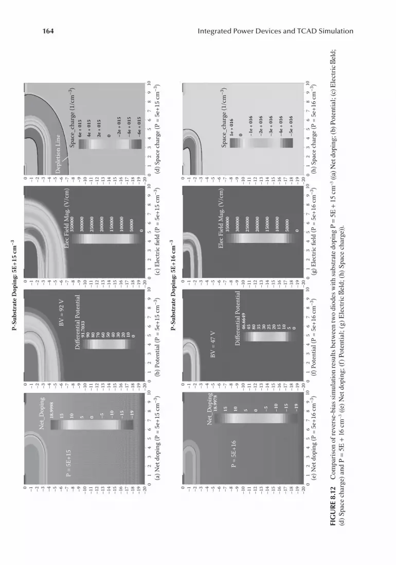
164 Integrated Power Devices and TCAD Simulation
P-Su
bstr
ate
Dop
ing:
5E+
15 cm
–3
P-Su
bstr
ate
Dop
ing:
5E+
16 cm
–3
Net
_Dop
ing
18.9
998
15 10 5 0 –5 –10
–15
–19
91.7
033
Diff
eren
tial P
oten
tial
Elec
Fie
ld M
ag. (
V/cm
)Sp
ace_
char
ge (1
/cm
–3)
6e +
015
4e +
015
2e +
015
0 –2e
+ 01
5
–4e
+ 01
5
–6e
+ 01
5
Dep
letio
n Li
ne
3500
00
3000
00
2500
00
2000
00
1500
00
1000
00
5000
0
0
BV =
92
VP
= 5E
+15
0
–20
01
23
45
67
89
100
12
34
56
78
910
01
23
45
67
89
100
12
34
56
78
910
01
23
45
67
89
100
12
34
56
78
910
01
23
45
67
89
100
12
34
56
78
910
–19
–18
–17
–16
–15
–14
–13
–12
–11
–10–9–8–7–6–5–4–3–2–1
0
–20
–19
–18
–17
–16
–15
–14
–13
–12
–11
–10–9–8–7–6–5–4–3–2–1
0
–20
–19
–18
–17
–16
–15
–14
–13
–12
–11
–10–9–8–7–6–5–4–3–2–1
0
–20
–19
–18
–17
–16
–15
–14
–13
–12
–11
–10–9–8–7–6–5–4–3–2–1
–20
–19
–18
–17
–16
–15
–14
–13
–12
–11
–10–9–8–7–6–5–4–3–2–1
00
–20
–20
–19
–18
–17
–16
–15
–14
–13
–12
–11
–10–9–8–7–6–5–4–3–2–1
0
–19
–18
–17
–16
–15
–14
–13
–12
–11
–10–9–8–7–6–5–4–3–2–1
0
–20
–19
–18
–17
–16
–15
–14
–13
–12
–11
–10–9–8–7–6–5–4–3–2–1
90 80 70 60 50 40 30 20 10 0
Net
_Dop
ing
18.9
978
15 10 5 0 –5 –10
–15
–19
46.6
649
Diff
eren
tial P
oten
tial
Elec
Fie
ld M
ag. (
V/cm
)Sp
ace_
char
ge (1
/cm
–3)
(h) S
pace
char
ge (P
= 5
e+16
cm–3
)(g
) Ele
ctric
fiel
d (P
= 5
e+16
cm–3
)(f)
Pot
entia
l (P
= 5e
+16
cm–3
)(e
) Net
dop
ing
(P =
5e+
16 cm
–3)
(d) S
pace
char
ge (P
= 5
e+15
cm–3
)(c
) Ele
ctric
fiel
d (P
= 5
e+15
cm–3
)(b
) Pot
entia
l (P
= 5e
+15
cm–3
)(a
) Net
dop
ing
(P =
5e+
15 cm
–3)
1e +
016
0 –1e
+ 01
6
–2e
+ 01
6
–3e
+ 01
6
–4e
+ 01
6
–5e
+ 01
6
3500
00
3000
00
2500
00
2000
00
1500
00
1000
00
5000
0
0
BV =
47
V
P =
5E+1
6
45 80 35 30 25 20 15 10 5 0
FIG
UR
E 8.
12
Com
pari
son
of re
vers
e-bi
as s
imul
atio
n re
sults
bet
wee
n tw
o di
odes
wit
h su
bstr
ate
dopi
ng P
= 5
E +
15
cm−3
((a)
Net
dop
ing;
(b)
Pot
enti
al; (
c) E
lect
ric
field
; (d
) Sp
ace
char
ge)
and
P =
5E +
16
cm–3
((e)
Net
dop
ing;
(f)
Pote
ntia
l; (g
) E
lect
ric
field
; (h)
Spa
ce c
harg
e)).

165Integrated Power Semiconductor Devices with TCAD Simulation
Figure 8.14, one can observe that in the higher-doping case the field is confined in the upper left corner, whereas the field in the low-doping case is more uniform. Just as we previously showed in our 1D model, the breakdown voltage is proportional to the integrated electric field ( ∫ EdS ), so having a more uniform field allows the region with a high electric field to contribute over a larger area, which tends to increase the breakdown voltage.
8.1.6.3 Breakdown Enhancement for Diode with NBLAs we have discussed before, without NBL and if the substrate is grounded, forward biasing the diode will instantly cause a high leakage current due to an internal short between the anode P-region
102
Diode Breakdown Voltage vs. P-Doping
P-Substrate Doping Concentration (cm–3)
Brea
kdow
n Vo
ltage
(V)
1E+14 1E+15 1E+16 1E+17
112
92
72
47
120
110
100
90
80
70
60
50
40
30
20
FIGURE 8.13 Breakdown voltage versus P-substrate doping concentration plot for PN junction diodes with-out NBL.
350000
Elec Field Mag. (V/cm)
y(micron)
P = 5E+16 cm–3
Elec Field Mag. (V/cm)
Surface Plots of Electric Field
300000 300000
250000
200000
150000
Anode
100000
50000
0
250000200000
150000100000
50000
0
–5
–10
–15
24
68
10
350000
Elec Field Mag. (V/cm)
y(micron)
P = 5E+15 cm–3
Elec Field Mag. (V/cm)300000 300000
250000
200000
150000
Anode
100000
50000
0
250000200000
150000
10000050000
0
–5
–10
–15
2
(b) Surface plot of electric eld (P = 5E+15 cm–3)(a) Surface plot of electric eld (P = 5E+16 cm–3)
46
810
FIGURE 8.14 Comparison of electric field 3D surface plots between two P-substrate doping concentrations at breakdown.
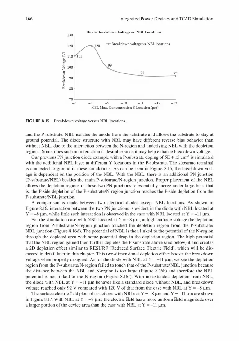
166 Integrated Power Devices and TCAD Simulation
and the P-substrate. NBL isolates the anode from the substrate and allows the substrate to stay at ground potential. The diode structure with NBL may have different reverse bias behavior than without NBL, due to the interaction between the N-region and underlying NBL with the depletion regions. Sometimes such an interaction is desirable since it may help enhance breakdown voltage.
Our previous PN junction diode example with a P-substrate doping of 5E + 15 cm−3 is simulated with the additional NBL layer at different Y locations in the P-substrate. The substrate terminal is connected to ground in these simulations. As can be seen in Figure 8.15, the breakdown volt-age is dependent on the position of the NBL. With the NBL, there is an additional PN junction (P-substrate/NBL) besides the main P-substrate/N-region junction. Proper placement of the NBL allows the depletion regions of these two PN junctions to essentially merge under large bias: that is, the P-side depletion of the P-substrate/N-region junction reaches the P-side depletion from the P-substrate/NBL junction.
A comparison is made between two identical diodes except NBL locations. As shown in Figure 8.16, interaction between the two PN junctions is evident in the diode with NBL located at Y = −8 µm, while little such interaction is observed in the case with NBL located at Y = −11 µm.
For the simulation case with NBL located at Y = −8 µm, at high cathode voltage the depletion region from P-substrate/N-region junction touched the depletion region from the P-substrate/NBL junction (Figure 8.16d). The potential of NBL is then linked to the potential of the N-region through the depleted area with some potential drop in the depletion region. The high potential that the NBL region gained then further depletes the P-substrate above (and below) it and creates a 2D depletion effect similar to RESURF (Reduced Surface Electric Field), which will be dis-cussed in detail later in this chapter. This two-dimensional depletion effect boosts the breakdown voltage when properly designed. As for the diode with NBL at Y = −11 µm, we see the depletion region from the P-substrate/N-region failed to touch that of the P-substrate/NBL junction because the distance between the NBL and N-region is too large (Figure 8.16h) and therefore the NBL potential is not linked to the N-region (Figure 8.16f). With no extended depletion from NBL, the diode with NBL at Y = −11 µm behaves like a standard diode without NBL, and breakdown voltage reached only 92 V compared with 120 V of that from the case with NBL at Y = −8 µm.
The surface electric field plots of structures with NBLs at Y = −8 µm and Y = −11 µm are shown in Figure 8.17. With NBL at Y = −8 µm, the electric field has a more uniform field magnitude over a larger portion of the device area than the case with NBL at Y = −11 µm.
120
Diode Breakdown Voltage vs. NBL Locations
Breakdown voltage vs. NBL locations
NBL Max. Concentration Y Location (µm)
Brea
kdow
n Vo
ltage
(V)
–7 –9–8 –10 –12–11 –13
111
99
92 92
130
120
110
100
90
80
70
FIGURE 8.15 Breakdown voltage versus NBL locations.

167Integrated Power Semiconductor Devices with TCAD SimulationN
BL L
ocat
ed a
t Y =
–8
um
NBL
Loc
ated
at Y
= –
11 u
m
Net
_Dop
ing
18.9
998
15 10 5 0 –5 –10
–15
–19
120.
362
120.
100.
Diff
eren
tial P
oten
tial
Elec
Fie
ld M
ag. (
V/cm
)
Spac
e_ch
arge
(1/c
m–3
)4e
+ 0
155e
+ 0
15
2e +
015
3e +
015
1e +
015
0 –1e
+ 01
5–2
e +
015
–4e
+ 01
5–3
e +
015
Spac
e_ch
arge
(1/c
m–3
)4e
+ 0
155e
+ 0
15
2e +
015
3e +
015
1e +
015
–1e
+ 01
50 –2
e +
015
–4e
+ 01
5–3
e +
015
Dep
letio
n Ed
ge
3500
00
3000
00
2500
00
2000
00
1500
00
1000
00
5000
0
0
BV =
120
V
NBL
(Y =
–8
um)
P =
5E+1
5
NBL
(Y =
–11
um
)
P =
5E+1
5
0
–20
01
23
45
67
89
100
12
34
56
78
910
01
23
45
67
89
100
12
34
56
78
910
01
23
45
67
89
100
12
34
56
78
910
01
23
45
67
89
100
12
34
56
78
910
–19
–18
–17
–16
–15
–14
–13
–12
–11
–10–9–8–7–6–5–4–3–2–1
0
–20
–19
–18
–17
–16
–15
–14
–13
–12
–11
–10–9–8–7–6–5–4–3–2–1
0
–20
–19
–18
–17
–16
–15
–14
–13
–12
–11
–10–9–8–7–6–5–4–3–2–1
0
–20
–19
–18
–17
–16
–15
–14
–13
–12
–11
–10–9–8–7–6–5–4–3–2–1
–20
–19
–18
–17
–16
–15
–14
–13
–12
–11
–10–9–8–7–6–5–4–3–2–10
0
–20
–19
–18
–17
–16
–15
–14
–13
–12
–11
–10–9–8–7–6–5–4–3–2–1
0
–19
–18
–17
–16
–15
–14
–13
–12
–11
–10–9–8–7–6–5–4–3–2–1
0
–20
–20
–19
–18
–17
–16
–15
–14
–13
–12
–11
–10–9–8–7–6–5–4–3–2–1
80 60 40 20 0
Net
_Dop
ing
18.9
998
15 10 5 0 –5 –10
–15
–19
91.6
517
Diff
eren
tial P
oten
tial
Elec
Fie
ld M
ag. (
V/cm
)
(h) S
pace
char
ge (N
BL Y
= –
11 u
m)
(g) E
lect
ric fi
eld
(NBL
Y =
–11
um
)(f
) Pot
entia
l (N
BL Y
= –
11 u
m)
(e) N
et d
opin
g (N
BL Y
= –
11 u
m)
(d) S
pace
char
ge (N
BL Y
= –
8 um
)(c
) Ele
ctric
fiel
d (N
BL Y
= –
8 um
)(b
) Pot
entia
l (N
BL Y
= –
8 um
)(a
) Net
dop
ing
(NBL
Y =
–8
um)
3500
00
3000
00
2500
00
2000
00
1500
00
1000
00
5000
0
0
BV =
92
V
90 80 70 60 50 40 30 20 10 0
FIG
UR
E 8.
16
(See
col
or in
sert
) C
ompa
riso
n pl
ots
of d
iffe
rent
NB
L lo
cati
ons
wit
h (a
) to
(d)
loca
ted
at Y
= −
8 µm
and
(e)
to (
h) lo
cate
d at
Y =
−11
µm
.
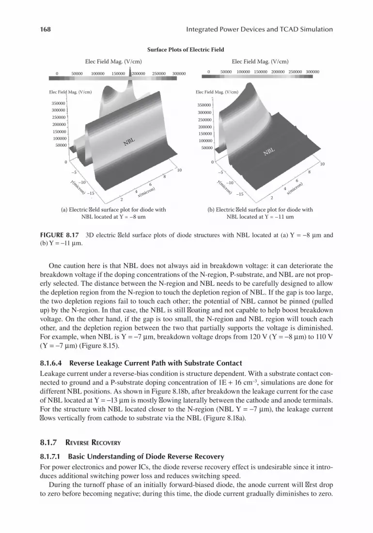
168 Integrated Power Devices and TCAD Simulation
One caution here is that NBL does not always aid in breakdown voltage: it can deteriorate the breakdown voltage if the doping concentrations of the N-region, P-substrate, and NBL are not prop-erly selected. The distance between the N-region and NBL needs to be carefully designed to allow the depletion region from the N-region to touch the depletion region of NBL. If the gap is too large, the two depletion regions fail to touch each other; the potential of NBL cannot be pinned (pulled up) by the N-region. In that case, the NBL is still floating and not capable to help boost breakdown voltage. On the other hand, if the gap is too small, the N-region and NBL region will touch each other, and the depletion region between the two that partially supports the voltage is diminished. For example, when NBL is Y = −7 µm, breakdown voltage drops from 120 V (Y = −8 µm) to 110 V (Y = −7 µm) (Figure 8.15).
8.1.6.4 Reverse Leakage Current Path with Substrate ContactLeakage current under a reverse-bias condition is structure dependent. With a substrate contact con-nected to ground and a P-substrate doping concentration of 1E + 16 cm−3, simulations are done for different NBL positions. As shown in Figure 8.18b, after breakdown the leakage current for the case of NBL located at Y = −13 µm is mostly flowing laterally between the cathode and anode terminals. For the structure with NBL located closer to the N-region (NBL Y = −7 µm), the leakage current flows vertically from cathode to substrate via the NBL (Figure 8.18a).
8.1.7 reverse recovery
8.1.7.1 Basic Understanding of Diode Reverse RecoveryFor power electronics and power ICs, the diode reverse recovery effect is undesirable since it intro-duces additional switching power loss and reduces switching speed.
During the turnoff phase of an initially forward-biased diode, the anode current will first drop to zero before becoming negative; during this time, the diode current gradually diminishes to zero.
Surface Plots of Electric Field
(a) Electric eld surface plot for diode withNBL located at Y = –8 um
(b) Electric eld surface plot for diode withNBL located at Y = –11 um
Elec Field Mag. (V/cm)
0 50000 100000 150000 200000 250000 300000 0
350000300000250000200000150000100000
50000
0
–5
–10
–152
4x(micron)
y(micron)
6
8
10
NBL
50000 100000 150000 200000 250000 300000
Elec Field Mag. (V/cm)
Elec Field Mag. (V/cm)
350000300000250000200000150000100000
50000
0
–5
–10
–152
4x(micron)
y(micron)
6
810
NBL
Elec Field Mag. (V/cm)
FIGURE 8.17 3D electric field surface plots of diode structures with NBL located at (a) Y = −8 µm and (b) Y = −11 µm.
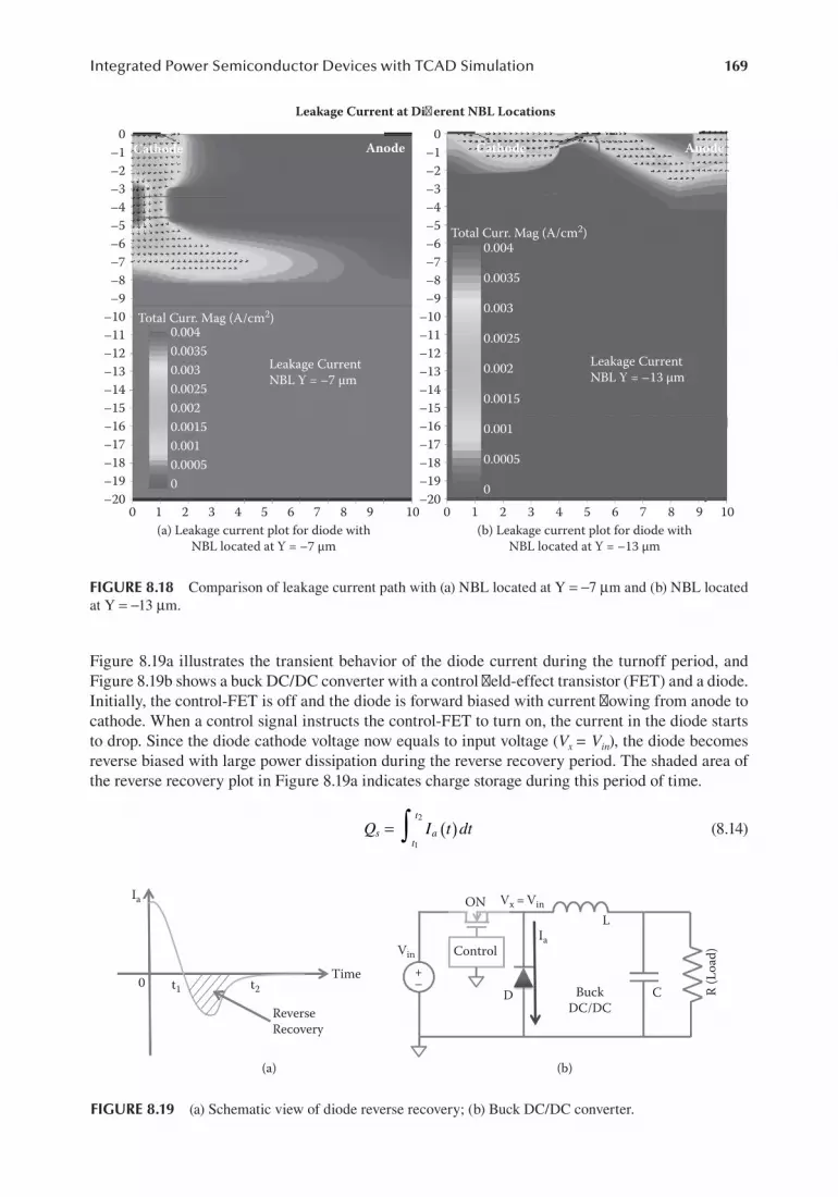
169Integrated Power Semiconductor Devices with TCAD Simulation
Figure 8.19a illustrates the transient behavior of the diode current during the turnoff period, and Figure 8.19b shows a buck DC/DC converter with a control field-effect transistor (FET) and a diode. Initially, the control-FET is off and the diode is forward biased with current flowing from anode to cathode. When a control signal instructs the control-FET to turn on, the current in the diode starts to drop. Since the diode cathode voltage now equals to input voltage (Vx = Vin), the diode becomes reverse biased with large power dissipation during the reverse recovery period. The shaded area of the reverse recovery plot in Figure 8.19a indicates charge storage during this period of time.
Q I t dts at
t∫ ( )=1
2
(8.14)
Leakage Current at Dierent NBL Locations
Total Curr. Mag (A/cm2)
Leakage CurrentNBL Y = –13 µm
AnodeCathode AnodeCathode
0.004
0.0035
0.003
0.0025
0.002
0.0015
0.001
0.0005
0
Total Curr. Mag (A/cm2)
Leakage CurrentNBL Y = –7 µm
0.0040.00350.0030.00250.0020.00150.0010.00050
0–1–2–3–4–5–6–7–8–9
–10–11–12–13–14–15–16–17–18–19–20
0 1 2 3 4 5(a) Leakage current plot for diode with
NBL located at Y = –7 µm(b) Leakage current plot for diode with
NBL located at Y = –13 µm
6 7 8 9 10 0 1 2 3 4 5 6 7 8 9 10
0–1–2–3–4–5–6–7–8–9
–10–11–12–13–14–15–16–17–18–19–20
FIGURE 8.18 Comparison of leakage current path with (a) NBL located at Y = −7 µm and (b) NBL located at Y = −13 µm.
Ia
t10 t2
ReverseRecovery
Time
(a) (b)
Vin Control
ON Vx = VinL
D CBuckDC/DC
R (L
oad)
Ia
+–
FIGURE 8.19 (a) Schematic view of diode reverse recovery; (b) Buck DC/DC converter.

170 Integrated Power Devices and TCAD Simulation
8.1.7.2 Diode Reverse Recovery TCAD SimulationFor power electronics engineers, the effects of diode reverse recovery on the circuit can be simu-lated with IC simulators (IC CAD tools) that solve compact device models. However, this kind of tool does not reveal the physics within the device. TCAD simulation is necessary for an in-depth understanding of what is going on during diode reverse recovery.
When the diode is forward biased (on-state), both electrons and holes contribute to the diode current. Electrons are injected into the P-side and holes injected into the N-side where they become minority carriers. When the diode is reverse biased (turned off), the minority carriers have finite time to be recombined or removed from either the N- or P-region. This finite time is called carrier lifetime (recombination lifetime). Minority carrier storage effect is more pronounced with lightly doped side.
In this simulation example, the P-substrate doping is 1E + 16 cm−3. The diode is first forward biased to Va = 1.5 V over a period of 1 ns and then reverse biased to Va = −5 V over a period of 5 ns, allowing sufficient time for the electrons to be removed. As can be seen from the simulation results in Figure 8.20, initially the diode is forward biased with anode voltage of 1.5 V from 0 to 1 ns. Starting from time 1 ns, a reverse bias is applied to the anode, and within another 1 ns, the anode current drops to zero and then reversely increases before finally decreases to reverse saturation leakage current.
Electron concentration plots under forward (Va = 1.5 V, time = 1 ns) and reverse (Va = −5 V, time = 6 ns) bias are shown in in Figure 8.21. Under forward bias right before turning off, there is a large electron concentration in the P-substrate (see PN junction line on the plot); under reverse bias and after the leakage current has stabilized to reverse saturation current, the electrons have been removed.
8.1.7.3 TCAD Simulations for Carrier Lifetime EngineeringAs we know, the diode reverse recovery is undesirable and should be minimized. One of the meth-ods of reducing the stored minority carriers is to reduce carrier lifetime. The most commonly used approach is to diffuse gold or platinum or to use electron irradiation to create recombination centers.
In a TCAD simulation, we can simulate this effect by simply modifying the minority carrier life-times and observing the results as seen in Figure 8.22. A shorter lifetime reduces the stored charges and allows lower switching power loss for power electronic systems.
8.1.8 scHottky diode
PN junction diode is a bipolar device in which both electrons and holes contribute to current flow. This bipolar action inevitably brings the problem of minority carrier storage and large reverse recov-ery power loss. Unlike the PN junction diode, a Schottky diode employs a metal-semiconductor junction, and only one type of carrier contributes to the total diode current: a unipolar device. Most
Anode Current Reverse Recovery
Anode Current
1000
80
60
40
20
0
–20
–40
–60
2000 3000 4000 5000 6000
Time (ps)Ano
de C
urre
nt (A
/m)
FIGURE 8.20 Transient simulation of diode reverse recovery.

171Integrated Power Semiconductor Devices with TCAD Simulation
of the time, a metal-to-N-type-semiconductor connection is used to construct the Schottky diode for power electronics and power IC applications.
For sufficiently low doping in the silicon, we neglect tunneling effects and from thermionic emis-sion theory, the I-V relation for the Schottky diode can be derived as
I I es
V
Va
t= −
1 (8.15)
Electron Concentration Plots during Reverse Recovery
Elec_Conc (E18/cm3)
P-Substrate(P = 1E+16)
ElectronConcentration@ Reverse Bias(Va = –5 V Vc = 0)
P-Substrate(P = 1E+16)
ElectronConcentration@ Forward Bias(Va = 1.5 V Vc = 0)
AnodeCathodeJunction Line *Electrons
Removed*
AnodeCathodeJunction Line
*InjectedElectrons*
0.001
0.0008
0.0006
0.0004
0.0002
0
Elec_Conc (E18/cm3)0.001
0.0008
0.0006
0.0004
0.0002
0
0–1–2–3–4–5–6–7–8–9
–10–11–12–13–14–15–16–17–18–19–20
0 1 2 3 4 5(a) Electron concentration plot at forward-
bias condition (Va = 1.5 V and Vc = 0V)(b) Electron concentration at reverse-bias
condition (Va = –5 V and Vc = 0V)
6 7 8 9 10 0 1 2 3 4 5 6 7 8 9 10
0–1–2–3–4–5–6–7–8–9
–10–11–12–13–14–15–16–17–18–19–20
FIGURE 8.21 Electron concentration plots at (a) forward and (b) reverse bias after the balance is established.
Reverse Recovery and Carrier Lifetime
Time (ps)
80
60
40
20
01,000 1,500 2,000 2,500 3,000 3,500 4,000 4,500 5,000 5,500 6,000
–20
–40
–60
Ano
de C
urre
nt (A
/m)
Default carrier lifetime
Carrier lifetime = 1E–10 sCarrier lifetime = 1E–9 sCarrier lifetime = 1E–8 s
FIGURE 8.22 Reverse recovery by using various carrier lifetimes.

172 Integrated Power Devices and TCAD Simulation
2I AKT es
V
Vbi
t=−
(8.16)
≈
K Acm
K100
2
2 (8.17)
where IS is the reverse saturation current, K is the Richardson constant, and Va is the applied voltage on the metal. Compared with the saturation current from the PN junction diode
= +
I AqnD
L N
D
L Ns PN i
p
p d
n
n a,
2 (8.18)
The reverse leakage current for a Schottky diode is almost always higher.One of the most important merits for a Schottky diode is the possibility of reducing the on-state
voltage drop. From our previous plots, we know there is always an approximate 0.7−0.8 V voltage drop for a PN junction diode (built-in potential for silicon). This drop can result in a large power loss for a power electronic system if the diode carries a large forward current. However, depending on the metal work function and the resulting barrier height, a Schottky diode may have a significantly lower turn-on voltage than a PN junction diode.
A Schottky diode is simulated with an N-type doping concentration of 5E + 16 cm−3 and vari-ous metal work functions. The schematic view of the structure is illustrated in Figure 8.23, and the simulation parameters are given in Table 8.3.
The simulated forward bias I-V curves are shown in Figure 8.24. For metals like Mg and Ti, the work functions are too small, whereas Pt has a turn-on voltage almost equal to the PN junction. The metals (Cr and W) in between provide a good balance between turn-on voltage and leakage current for this case.
As an example, two band diagrams, one for Gold (Au) and one for Tungsten (W), are plotted in Figure 8.25 at the Schottky junctions, with the cutline located between points of (X = 0.1 Y = 0) and (X = 0.1 Y = −0.25).
AnodeCathode
Schottky Diode Schematic and Simulated Net Doping
Anode Cathode
Contact work functionmodified to representdifferent metals
Net_Doping
N+N+ Contact
(a) Schottky diode schematic structure (b) Schottky diode simulated net doping
+Y
0
–1
–2
–3
–4
–5
–6
–7
–8
–9
–100 1 2 3 4 5 6 7 8 9 10
20
15
10
5
0
Metal
N-Substrate(5E+16 cm–3)
FIGURE 8.23 Schottky diode schematic and simulation structures.

173Integrated Power Semiconductor Devices with TCAD Simulation
TABLE 8.3Simulation Parameters for a Schottky Diode
Parameters for Simulation Value
X range 0 to 10 µm
Y range 0 to −10 µm
P-substrate (P-base constant doping) 5E + 16 cm−3
Metal Schottky contact anode (x1, x2) (0, 1)
Ohmic contact cathode (x1, x2) (9, 10)
Comparison of Forward-Biased Schottky JunctionDiodes with Different Metal Anodes
Mg 3.7 VTi 4.3 VCr 4.5 VW 4.6 VAu 5.1 VPt 5.7 VPN junction
400
350
300
250
200
150
100
50
00.0 0.2 0.4 0.6
Anode Voltage (V)
Colle
ctor
Cur
rent
(A/m
)
0.8 1.0 1.2
FIGURE 8.24 Forward-biased Schottky diode with various metal work functions.
AuWork Function = 5.1
(a) Schottky junction band diagram for Au
Band Diagram of Schottky Diodes with Dierent Metal Work Functions
Ener
gy (e
v)
Ener
gy (e
v)
(b) Schottky junction band diagram for WDistance (um) Distance (um)
WWork Function = 4.6
Band DiagramBand Diagram
E_vE_fE_c
E_vE_fE_c
0.250.20.150.10.0500.250.20.150.10.050–0.9–0.8–0.7–0.6–0.5–0.4–0.3–0.2–0.1
00.10.20.30.40.5
–0.9–0.8–0.7–0.6–0.5–0.4–0.3–0.2–0.1
00.10.20.30.40.50.60.70.80.9
1
FIGURE 8.25 Schottky junction band diagrams plotted for Au and W.

174 Integrated Power Devices and TCAD Simulation
8.1.9 zener diode
When doping concentrations on both sides of the PN junctions are high, another type of break-down called Zener breakdown occurs. Different from avalanche breakdown, which is due to impact ionization, Zener breakdown happens at low voltages by direct interband (conduction ↔ valence) tunneling of carriers. Zener diodes are useful in many applications for analog and power IC, espe-cially for clamping the gate voltage of a power DMOS. Figure 8.26a shows the schematic view, and Figure 8.26b is the net doping plot of the Zener diode simulated structure. For a successful simula-tion of a Zener diode, the mesh surrounding the P+/N+ junction should be extra dense to correctly model the tunneling. The simulation parameters are given in Table 8.4.
Shown in Figure 8.27 are linear and log scale of breakdown curves for different doping concen-trations. We can see that the Zener breakdown curve is quite “soft,” without a sharp corner or steep current increase: this is typical of a tunneling effect. In practice, Zener diodes with breakdown ranges from 3 V to 6 V are available. Zener diodes with a breakdown larger than 6 V are usually not considered a “pure” Zener since they also have significant impact ionization. In real fabrication, junctions formed by very high doping concentrations usually come with large damage and disloca-tions. This is especially true if both high-dose and high-energy implants are performed.
The band diagrams of Zener diodes with two doping concentration levels (Na = Nd = 5E + 19 cm−3 and Na = Nd = 5E + 18 cm−3) at breakdown are shown in Figure 8.28. At larger doping values, the
Anode Cathode
Schottky Diode Schematic and Simulated Structure Views
(a) Schottky diode schematic structure (b) Schottky diode simulated structure
0
–1
–2
–3
–4
–5
–6
–7
–8
–9
–100 1 2 3 4 5 6 7 8 9 10
Net_Doping20
1015
05
–10–5
–15–20
P+ N+Cathode Anode
N+ P+
P-Substrate(5E+16 cm–3)
Extra fine mesh shouldbe placed at P/N junction
area for Zener diodesimulation
FIGURE 8.26 Zener diode schematic view and net doping plot of the simulated structure.
TABLE 8.4Simulation Parameters List for Zener Diode
Parameters for Simulation Value
X range 0 to 10 µm
Y range 0 to −10 µm
P-substrate (P-base constant doping) 5E + 16 cm−3
N+ region max concentration 5E + 19 cm−3
N+ region location (x1, x2, dx1, dx2) Gaussian X = (0, 5, 0, 0); Y = (−0.5, 0, 0, 0)
P+ region max concentration 5E + 19 cm−3
P+ region location (x1, x2, dx1, dx2) Gaussian X = (5, 10, 0, 0); Y = (−0.5, 0, 0, 0)

175Integrated Power Semiconductor Devices with TCAD Simulation
proximity of empty states on the other side of the junction makes it very easy for carriers to tunnel from band to band.
8.1.10 smAll signAl model For pn Junction diode
I-V curves of semiconductor devices are generally nonlinear. For example, the forward I-V curve of a diode is nonlinear if we look at a large voltage span. However, if we take an infini-tesimal portion of this nonlinear curve, as shown in Figure 8.29, we can linearize the nonlinear device. A small signal model is based on such a linearization around a bias point Q, which is the DC voltage/current level when no signal is applied. Small signal models are very useful tools for analog and power IC design.
Figure 8.30 is the small signal representation of a diode, which can be viewed as a capaci-tor and resistor connected in parallel: the resistor is the parasitic resistance of the PN junction diode, while the capacitor represents a combination of junction capacitance and diffusion capacitance [167].
0.014
0.012
0.010
0.008
0.006
0.004
0.002
0.0000 1 2
Cathode Voltage (V)(a) I-V curves of Zener diode in linear scale (b) I-V curves of Zener diode in log scale
Cath
ode C
urre
nt (A
/m)
Cath
ode C
urre
nt (A
/m)
Cathode Voltage (V)3 4 5 0 1 2 3 4 5
0.1 Log Scale
Na = Nd = 5E+19Na = Nd = 1E+19Na = Nd = 5E+18
Na = Nd = 5E+19Na = Nd = 1E+19Na = Nd = 5E+18 0.01
1E–31E–4
1E–71E–61E–5
1E–91E–8
1E–101E–11
FIGURE 8.27 Zener breakdown comparison with different doping concentrations.
Band Diagrams of Zener Diodes at Breakdown
Band Diagram
Ener
gy (e
v)
1
0 Na = Nd = 5E+18 cm–3Na = Nd = 5E+19 cm–3
–1
–2
–3
–4
–5
E_vE_fE_c
Band Diagram
Ener
gy (e
v)
1
0.5
0
–0.5
–1
–1.5
–2
0.02 0.04 0.06 0.08 0.1Distance (um) Distance (um)
(a) Band diagram of Zener diode with Na = Nd = 5e+19 cm–3 at breakdown
(b) Band diagram of Zener diode with Na = Nd = 5e+18 cm–3 at breakdown
0.12 0.14 0.16 0.18 0.02 0.04 0.06 0.08 0.1 0.12 0.14 0.16 0.18
E_vE_fE_c
FIGURE 8.28 Band diagram of Zener diode at the PN junction at breakdown with (a) Na = Nd = 5E + 19 cm−3 and (b) Na = Nd = 5E + 18 cm−3.

176 Integrated Power Devices and TCAD Simulation
The small signal conductance and resistance can be calculated as
gdIdV
dIdV
dI edV
dI edV
qkT
I eq
kTI
IV
a
a
s
qV
kT
a
s
qV
kT
as
qV
kTa
a
t
a aa
= = = ⋅ −
≈ ⋅ = ⋅ = =
1
(8.19)
1
Rg
VI
t
a
= = (8.20)
There are two capacitance components for a diode. The first one is the junction capacitance, which dominates the reverse bias and small forward-bias region. The other component is called dif-fusion capacitance and is caused by charge storage effects during the diffusion process; it dominates the large forward-bias region. The total capacitance from both effects can be calculated as
C C CAW
dIdV
A
V Vq N N
IV
junction diffusions
sa
a
s
s bi a
a d
sa
t
= + = ε + τ = εε − +
+ τ2 ( ) 1 1
(8.21)
This equation should be used with caution because the equation for the junction capacitance is valid only when V Va bi< . If the applied voltage is higher, the total capacitance is dominated by the
I
V
A very smallportion of anonlinearcurve can beviewed aslinear
Q (DC Bias Point)
FIGURE 8.29 Small signal analysis.
D
I
C R
+
V
–
FIGURE 8.30 Small signal representation of a PN junction diode.

177Integrated Power Semiconductor Devices with TCAD Simulation
diffusion capacitance, and the junction capacitance should diminish rather than going to infinity as predicted by the equation. The diode capacitance is simulated with TCAD, and the result is shown in Figure 8.31. Junction capacitance dominates when the applied anode voltage is smaller than the built-in potential; after the built-in potential is reached, the junction capacitance drops, and the dif-fusion capacitance picks up rapidly with applied anode voltage.
8.2 BIPOLAR JUNCTION TRANSISTORS
The BJT was first invented in 1948 at Bell Labs. Bipolar refers to the fact that both electrons and holes participate in the transistor operation, contrary to unipolar devices like MOSFETs and Schottky diodes. Before the wide acceptance of CMOS technologies, BJT dominated the semiconductor industry; CMOS gradually replaced BJTs in digital ICs thanks to the latter’s advantages in high density, scaling capabil-ity, and low power gate drive. BJTs are still preferred in many high-frequency and analog applications for their merits of high speed, low noise, good matching, and high output power.
Two types of BJTs are available: NPN and PNP. NPN BJTs have N+ emitter, P-type base, and N-type collector; PNP BJTs have P+ emitter, N-type base, and P-type collector. Due to the higher mobility of electrons, NPNs are generally preferred over PNPs, so this section discusses only NPN transistors. A simplified NPN BJT structure can be visualized (Figure 8.32) as two back-to-back diodes with a P-region sandwiched between two N-regions.
1600
1400
1200
1000
800
600
400
200
00 0.1 0.2
Junction capacitance dominates until Vareaches built-in potential
PN Junction Diode Parasitic Capacitance
Anode Voltage Va (V)
Capa
cita
nce (
nF/m
)
Diffusioncapacitancedominates
at higher Varegion
0.3 0.4 0.5 0.6 0.7 0.8 0.9
FIGURE 8.31 TCAD simulation of PN junction diode capacitance.
NCollector
PBase
N+Emitter
FIGURE 8.32 Basic structure of an NPN BJT.

178 Integrated Power Devices and TCAD Simulation
8.2.1 BAsic operAtion oF npn BJts
8.2.1.1 Simulation StructureThe schematic structure of an NPN transistor is shown in Figure 8.33a. Since this structure is symmetrical, it can be truncated for simulation purposes. By simulating only half of the struc-ture, as seen in Figure 8.33b, results can be obtained faster by using less computer memory and processing power.
In this simulation example, a lateral NPN BJT is created with an NBL connected to the N col-lector through an N link implant, which can be created by an implant chain of high- and low-energy ion implants. The base P-region can be created either with P-substrate, P-epi layer, or an implanted P-well. For the sake of simplicity, in the simulation a P-substrate is used. The simulation parameters for this NPN BJT are listed in Table 8.5 (N+ and P+ contacts are omitted).
The simulated NPN BJT net doping plot is illustrated in Figure 8.34a with a 3D surface plot of net doping in Figure 8.34b. The surface plot eliminated the substrate below y = −10 µm, since the most important device information is located above y = −10 µm.
Band diagrams at equilibrium are illustrated in Figure 8.35. Since the BJT has N-P-N structures in both horizontal and vertical directions, a horizontal band diagram is shown with a cutline located from (x = 0, y = −1) to (x = 10, y = −1), and a vertical band diagram is shown with a cutline located from (x = 9, y = 0) to (x = 9 y = −10).
(a) Schematic representation of NPN BJT with full structure (b) Half structure for simulation
P-Substrate
NBL/Collector
P-Substrate
NBL/Collector
N LinkN LinkN Link
Base EmitterCollector
Base EmitterCollectorBaseBase Emitter CollectorCollector
BaseBase Emitter CollectorCollector
FIGURE 8.33 Schematic representation of NPN BJT with (a) full structure and (b) half structure for simulation.
TABLE 8.5NPN BJT Simulation Parameters List
Parameters for Simulation Value
X range 0 to 10 µm
Y range 0 to −20 µm
P-substrate 1E + 15 cm−3
P-base doping 1E + 17 cm−3
NBL max concentration 1E + 16 cm−3
NBL location (x1, x2, dx1, dx2) Gaussian x = (0, 10, 1, 1); y = (−7, −7, 1, 1)
N-link max concentration 1E + 16 cm−3
N-link location (x1, x2, dx1, dx2) Gaussian x = (0, 4, 0.25, 0.25); y = (−6, 0, 0.25, 0.25)
Emitter N-well max 1E + 19 cm−3
Emitter N-well location (x1, x2, dx1, dx2) Gaussian x = (6.5, 10, 0.25, 0.25); y = (−0.5, −0.5, 0.5, 0.5)

179Integrated Power Semiconductor Devices with TCAD Simulation
NPN BJT Net Doping Plots
NBL
Emitter
Log10 (Net_Doping)Log10 (Net_Doping)
20
15
10
5
010
1816141210
8642
0–2
–4–6
–8
y(micron)
8
64
x(micron)
Collector
(1E+16 cm–3 )
Base
(1E+17 cm–3 )
Emitter
(1E+19 cm–3 )
2
Collector Base
Net_Doping20
15
10
5
0
–10
–5
–20
–15
0–1–2–3–4–5–6–7–8–9
–10–11–12–13–14–15–16–17–18–19–20
0 1 2 3 4 5(a) Net doping plot of NPN BJT
(b) Surface plot of net doping plot of NPN BJT
6 7 8 9 10
FIGURE 8.34 (a) Simulated net doping plot and (b) 3D net doping surface plot of an NPN BJT.
Band Diagram Plots
Equilibrium Condition
Cutline (9,0) to (9,–10)
Cut l
ine (
0,–1
) to
(10,
–1)
Dist
ance
(um
)
Energy (eV)
Ener
gy (e
V)
Band
Dia
gram
Base
Colle
ctor
Emitt
erBaseCollector Emitter
BaseCollector
0.5
0
–0.5
–1
–1
–2
–3
–4
–5
–6
–7
–8
–9
–10
0
0 2 4 6 8 10
0.5 0 –0.5 –10
2
4
6
8
10
Emitter
E_v
E_f
E_c
Band Diagram
Conduction Band
Valence Band
Distance (um)
E_vE_fE_c
FIGURE 8.35 Band diagram plot of NPN BJT at equilibrium.

180 Integrated Power Devices and TCAD Simulation
8.2.1.2 Collector and Base CurrentIf a small positive voltage is applied to the collector with all other terminals grounded, the base/collector PN junction is reverse biased, and no current flows except leakage current. When the base/emitter PN junction is forward biased by applying a positive voltage at the base terminal with respect to emitter terminal, holes are injected into the N+ emitter, and electrons are injected into the P-base. Unlike a PN junction diode where electrons enter the P-region and are extracted by the anode terminal, electrons that injected into the base are swept to the collector by the electric field in the depletion region created by the reverse-biased base/collector PN junction. After electrons reach the collector region they will be attracted and collected by the positively biased collector contact. This electron current contributes to collector current Ic, which is independent of the collector bias as long as the base/collector junction is reverse biased.
The collector current is dominated by the diffusion of electrons from emitter to base. Assuming low-level injection (injected minority carrier level is much less than a majority carrier doping con-centration) and constant base doping, the collector current Ic can be expressed as [167].
= ⋅ −
= −
I I e A q
D
W
n
Nec s
V
VE
B
B
i
B
V
VBE
t
BE
t1 12
(8.22)
where IS is the saturation current, VBE is base to emitter voltage, AE is the emitter area, ni is the intrin-sic carrier concentration Vt is the thermal voltage, WB is the base width, and DB is the minority carrier diffusion coefficient in the base region. At high VBE, the injected minority carrier (electrons in the base region of the NPN transistor) density becomes equal or even larger than majority carrier density (holes in the NPN base region), so the collector current needs some modifications:
2I n ec i
V
VBE
t∝
(8.23)
The base current Ib is created by holes injected into the emitter region. Similar to Ic, Ib, is diffuse dominated and can be expressed as
I A qDW
nN
eb EE
E
i
E
V
VBE
t= −
12
(8.24)
where DE is the diffusion coefficient of minority carriers (holes in NPN) in the emitter, WE is emitter width, and NE is the constant doping concentration in the emitter. Since the emitter is usually heavily doped, it is not easy to reach a high injection level in the emitter.
8.2.1.3 Transistor Gain and Gummel PlotOne of the most important design parameters for BJTs is the DC current gain β, which is defined as
II
D W ND W N
c
b
B E E
E B B
β = = (8.25)
In TCAD simulation, to obtain the current gain a positive bias of 1.0 V is applied to the collector, and then base voltage is scanned from 0 to 1.2 V. The emitter terminal is always grounded. Using the NPN simulation structure described earlier in this chapter, Ic and Ib plots versus VBE are plotted on

181Integrated Power Semiconductor Devices with TCAD Simulation
log(Y)-linear(X) scale (Gummel plot) on Figure 8.36a; the resulting DC current gain β is also included (Figure 8.36b).
8.2.2 npn BJt BreAkdown
Since a BJT is a three-terminal device, breakdown can happen between any of the reverse-biased PN junctions or any combination. The four most useful breakdown analyses are BVCBO, BVEBO, BVCEO, and BVCES.
8.2.2.1 BVCBO
Here, BV is short for breakdown voltage, and CBO means breakdown between collector (N-type) and base (P-type) with emitter (N-type) terminal open (floating): BVCBO is the breakdown voltage of the base/collector PN junction with no influence from the emitter, so it is similar to a regular PN junction diode breakdown. Figure 8.37a is the potential plot of BVCBO, we see the break-down voltage between collector and base with emitter open is 64 V. Figure 8.37b–f plot the electric field, space charge, impact ionization, electron current magnitude, and hole current magnitude. The impact ionization takes place at the collector/base junction close to the surface.
8.2.2.2 BVEBO
EBO means breakdown between emitter (N-type) and base (P-type) with collector terminal open (floating). Similar to BVCBO, BVEBO is just the breakdown voltage of base/emitter PN junction with no influence from the collector. Figure 8.38a is the potential plot of BVEBO, with a simulated break-down voltage of only 21 V. The low breakdown voltage between emitter and base with collector open is easily understandable since the emitter is a heavily doped region (at about 1E + 19 cm−3) and the base doping is about 1E + 17 cm−3. Figure 8.38b–f are plots of electric field, space charge, impact ionization, electron current magnitude, and hole current magnitude. We see the impact ionization happens at the base/emitter junction close to the silicon surface.
8.2.2.3 BVCEO
CEO means breakdown between collector (N-type) and emitter (N-type) with base open (floating). Unlike BVCBO and BVEBO, BVCEO involves two PN junctions. BVCEO may be the most important
BJT Gummel Plot and DC Current Gain
Gummel Plot of an NPN BJT BJT DC Current Gain600
500
400
300
200
100
0
1.00E–11
1.00E–09
1.00E–07
1.00E–05
1.00E–03
1.00E–01
1.00E+01
1.00E+03
1E+04
1E+021E+03
1E–051E–041E–031E–021E–011E+001E+01
1E–061E–07
1E–101E–091E–08
1E–121E–11
Collector Current Ic (A/m)
0.00 0.20 0.40 0.60 0.80 1.00 1.20
(b) BJT DC current gain
BJT
DC
Curr
ent G
ain
I c an
d I b
(A/m
) with
Log
Sca
le
Base to Emitter Voltage VBE (V)(a) Gummel plot
FIGURE 8.36 Gummel plot and DC current gain plot.

182 Integrated Power Devices and TCAD Simulation
breakdown voltage in BJTs: it usually has a low breakdown voltage value due to the BJT current amplification effect. When a positive bias is applied to the collector and the emitter is grounded, the collector/base junction is always reverse biased. The potential of the emitter is pinned to zero by grounding the emitter contact. Since the base contact is floating, the base potential is linked to the collector potential minus the voltage drop across the depletion region. If somehow the base potential is higher than the built-in potential of the base/emitter PN junction, the base to emitter junction is then forward biased. Due to the current amplification effect of a BJT transistor, the device operates with current gain that increases with increasing collector current. This positive feedback mechanism produces a collapse in the voltage that can be supported by the transistor and leads to a lower break-down voltage [158]. Figure 8.39a shows the potential plot of BVCEO with a simulated breakdown voltage of 29 V. Figures 8.39b–f plot the electric field, space charge, impact ionization, electron current magnitude, and hole current magnitude. We note that the impact ionization takes place at the
NPN BJT at BVcbo Breakdown
BaseCollector Emitter BaseCollector Emitter
BaseCollector Emitter BaseCollector Emitter
BaseCollector Emitter BaseCollector Emitter
–1–2–3–4–5–6–7–8–9
–10
0–1–2–3–4–5–6–7–8–9
–10
0
–1–2–3–4–5–6–7–8–9
–10
0–1–2–3–4–5–6–7–8–9
–10
0
–1–2–3–4–5–6–7–8–9
–10
0–1–2–3–4–5–6–7–8–9
–10
0
0 1 2 3
Elec Field Mag. (V/cm)
BVcbo = 64 V300000
400000
350000
250000
200000
150000
50000
100000
0
1e+025
Impact_Ionization(1/cm3/s)
8e+024
6e+024
4e+024
2e+024
0
1e+015
Space_Charge(1/cm–3)
5e+014
0
–5e+014
–1e+015
200
Hole Curr. Mag(A/cm2)
150
100
50
0
200
Elec. Curr. Mag(A/cm2)
150
100
50
0
4(a) Potential plot (b) Electric field plot
(c) Space charge plot (d) Impact ionization plot
(e) Electron current magnitude plot (f ) Hole current magnitude plot
5 6 7 8 109
0 1 2 3 4 5 6 7 8 109
0 1 2 3 4 5 6 7 8 109
0 1 2 3 4 5 6 7 8 109
0 1 2 3 4 5 6 7 8 109
0 1 2 3 4 5 6 7 8 109
Differential Potential63.9501
60
50
40
30
20
10
0
–0.0144825
FIGURE 8.37 Simulation plots at BVCBO breakdown.
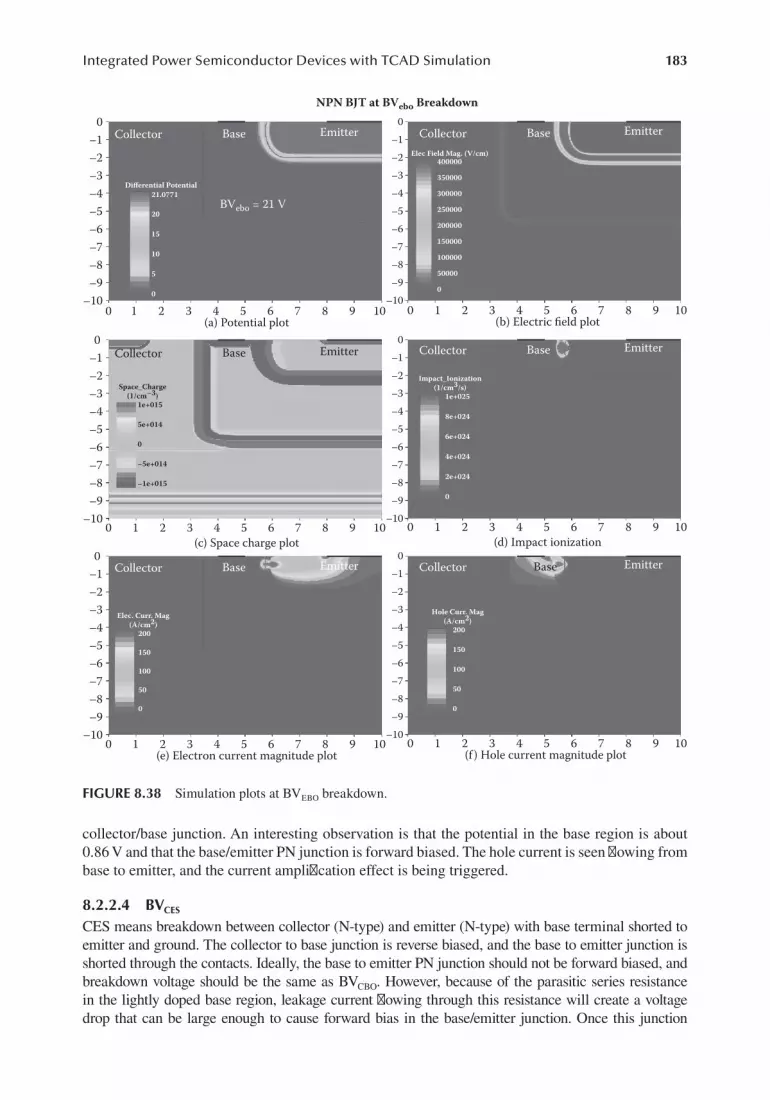
183Integrated Power Semiconductor Devices with TCAD Simulation
collector/base junction. An interesting observation is that the potential in the base region is about 0.86 V and that the base/emitter PN junction is forward biased. The hole current is seen flowing from base to emitter, and the current amplification effect is being triggered.
8.2.2.4 BVCES
CES means breakdown between collector (N-type) and emitter (N-type) with base terminal shorted to emitter and ground. The collector to base junction is reverse biased, and the base to emitter junction is shorted through the contacts. Ideally, the base to emitter PN junction should not be forward biased, and breakdown voltage should be the same as BVCBO. However, because of the parasitic series resistance in the lightly doped base region, leakage current flowing through this resistance will create a voltage drop that can be large enough to cause forward bias in the base/emitter junction. Once this junction
NPN BJT at BVebo Breakdown
BaseCollector Emitter BaseCollector Emitter
BaseCollector Emitter BaseCollector Emitter
BaseCollector Emitter BaseCollector Emitter
–1–2–3–4–5–6–7–8–9
–10
0–1–2–3–4–5–6–7–8–9
–10
0
–1–2–3–4–5–6–7–8–9
–10
0–1–2–3–4–5–6–7–8–9
–10
0
–1–2–3–4–5–6–7–8–9
–10
0–1–2–3–4–5–6–7–8–9
–10
0
0 1 2 3
Differential Potential
Elec Field Mag. (V/cm)
21.0771BVebo = 21 V
20
15
10
5
0
300000
400000
350000
250000
200000
150000
50000
100000
0
1e+025
Impact_Ionization(1/cm3/s)
8e+024
6e+024
4e+024
2e+024
0
1e+015
Space_Charge(1/cm–3)
5e+014
0
–5e+014
–1e+015
200
Hole Curr. Mag(A/cm2)
150
100
50
0
200
Elec. Curr. Mag(A/cm2)
150
100
50
0
4(a) Potential plot (b) Electric field plot
(c) Space charge plot (d) Impact ionization
(e) Electron current magnitude plot (f ) Hole current magnitude plot
5 6 7 8 109
0 1 2 3 4 5 6 7 8 109
0 1 2 3 4 5 6 7 8 109
0 1 2 3 4 5 6 7 8 109
0 1 2 3 4 5 6 7 8 109
0 1 2 3 4 5 6 7 8 109
FIGURE 8.38 Simulation plots at BVEBO breakdown.

184 Integrated Power Devices and TCAD Simulation
is forward biased, the leakage current gets amplified, just like the case of BVCEO. However, a properly designed P-type base with sufficiently high doping will reduce the resistance and minimize this effect. Figure 8.40a is the potential plot with a breakdown voltage of 64 V, the same as BVCBO because the breakdown occurs once again between the collector and grounded (shorted) base. Figures 8.40b–f plot the electric field, space charge, impact ionization, electron current magnitude, and hole current magni-tude. These plots are very similar to the plots found in Figure 8.37 for BVCBO. Compared with BVCES, the base potential is at 0 V, which means that thanks to the high doping in the P-base region the base/emitter parasitic diode is not turned on. The hole current flow is induced by impact ionization only and is not flowing from base to emitter.
8.2.2.5 Comparison of the Four Types of NPN BreakdownThe simulation result for BVCES is similar to BVCBO because with high P-base doping (about 1E + 17 cm−3), the base to emitter PN junction is not turned on by the leakage current flowing through the collector to
NPN BJT at BVceo Breakdown
BaseCollector Emitter BaseCollector Emitter
BaseCollector Emitter BaseCollector Emitter
BaseCollector Emitter BaseCollector Emitter
–1–2–3–4–5–6–7–8–9
–10
0–1–2–3–4–5–6–7–8–9
–10
0
–1–2–3–4–5–6–7–8–9
–10
0–1–2–3–4–5–6–7–8–9
–10
0
–1–2–3–4–5–6–7–8–9
–10
0–1–2–3–4–5–6–7–8–9
–10
0
0 1 2 3
Dierential Potential Elec Field Mag. (V/cm)28.7953
BVceo = 29 V25
15
20
10
5
0
300000
400000
350000
250000
200000
150000
50000
100000
0
1e+023
Impact_Ionization(1/cm3/s)
8e+022
6e+022
4e+022
2e+022
0
1e+015
Space_Charge(1/cm–3)
5e+014
0
–5e+014
–1e+015
1.6
Hole Curr. Mag(A/cm2)
1.4
1.2
1
0.8
0.6
0.4
0.2
0
200
Elec. Curr. Mag(A/cm2)
150
100
50
0
4(a) Potential plot (b) Electric eld plot
(c) Space charge plot (d) Impact ionization plot
(e) Electron current magnitude plot (f ) Hole current magnitude plot
5 6 7 8 109
0 1 2 3 4 5 6 7 8 109
0 1 2 3 4 5 6 7 8 109
0 1 2 3 4 5 6 7 8 109
0 1 2 3 4 5 6 7 8 109
0 1 2 3 4 5 6 7 8 109
FIGURE 8.39 Simulation plots at BVCEO breakdown.

185Integrated Power Semiconductor Devices with TCAD Simulation
the base. BVCEO simulation yields a 29 V breakdown voltage, which is due to the aforementioned current amplification effect. The BVEBO in our simulation case has the lowest breakdown voltage of only 21 V. This is caused by the highly doped and abrupt emitter/base PN junction: if the emitter doping concentration were more graded, the BVEBO breakdown voltage would be higher. A comparison of breakdown voltages for our NPN BJT is given in Figure 8.41.
8.2.3 BJt i-v FAmily oF curves
Unlike MOSFETs that are turned on by applying a constant gate voltage, BJTs are driven by constant base current. The IC-VCE curves with different base bias current (IB) are shown in Figure 8.42. For simu-lation purposes, the base current is first scanned to a certain value, and then the collector voltage is ramped up while the base current held constant. Incremental base current (IB) generates a series of I-V curves. We can see these curves are not exactly flat and they are dependent on collector voltage (VCE); this dependence is called the Early effect, named after Dr. James Early. Put simply, a higher voltage on
NPN BJT at BVces Breakdown
BaseCollector Emitter BaseCollector Emitter
BaseCollector Emitter BaseCollector Emitter
BaseCollector Emitter BaseCollector Emitter
–1–2–3–4–5–6–7–8–9
–10
0–1–2–3–4–5–6–7–8–9
–10
0
–1–2–3–4–5–6–7–8–9
–10
0–1–2–3–4–5–6–7–8–9
–10
0
–1–2–3–4–5–6–7–8–9
–10
0–1–2–3–4–5–6–7–8–9
–10
0
0 1 2 3
Differential PotentialElec Field Mag. (V/cm)70
BVces = 64 V
60
50
40
0
10
20
30
300000
400000
350000
250000
200000
150000
50000
100000
0
1e+025
Impact_Ionization(1/cm3)
8e+024
6e+024
4e+024
2e+024
0
1e+015
Space_Charge(1/cm3)
5e+014
0
–5e+014
–1e+015
200
Hole Curr. Mag(A/cm2)
150
100
50
0
200
Elec. Curr. Mag(A/cm2)
150
100
50
0
4(a) Potential plot (b) Electric field plot
(c) Space charge plot (d) Impact ionization plot
(e) Electron current magnitude plot (f) Hole current magnitude plot
5 6 7 8 109
0 1 2 3 4 5 6 7 8 109
0 1 2 3 4 5 6 7 8 109
0 1 2 3 4 5 6 7 8 109
0 1 2 3 4 5 6 7 8 109
0 1 2 3 4 5 6 7 8 109
FIGURE 8.40 Simulation plots at BVCES breakdown.

186 Integrated Power Devices and TCAD Simulation
the collector causes the depletion region in collector/base PN junction to widen, which squeezes the base width (calculated using the base metallurgical width minus base depletion width). This decrease of base width gives rise to extra collector current. The Early effect is not desirable and should be kept as small as possible; however, modern technology requires a small base width to boost the current gain, which invari-ably means that the devices suffer from a more severe Early effect unless proper precautions are taken. As seen in Figure 8.43, with a high P-base doping concentration the depletion region spreads mostly in the collector region: only a very small space charge width increase can be observed in the base, which explains why the simulated IC-VCE curves are almost flat.
8.2.4 kirk eFFect
To explain the Kirk effect (base push-out effect), let us first look at the relationship between current density and doping concentration. The maximum current density under certain doping concentra-tion in the collector is expressed as
J qnvc sat= (8.26)
0
Breakdown
Brea
kdow
n Vo
ltage
(V)
10
20
30
40
50
60
70NPN BJT Breakdown Comparison
BVCEO29
BVEBO21
BVCEO64
BVCBO64
FIGURE 8.41 NPN BJT breakdown comparison chart.
14
Ic – Vce Family of Curves
Collector to Emitter Voltage Vce (V)
Col
lect
or C
urre
nt I c
(A/m
)
0 1 2 3 4 5
Ib = 0.01 A/mIb = 0.02 A/mIb = 0.03 A/mIb = 0.04 A/mIb = 0.05 A/m
12
10
8
6
4
2
0
FIGURE 8.42 Simulated BJT I-V family of curves with Ib from 0.01 A/m to 0.05 A/m.

187Integrated Power Semiconductor Devices with TCAD Simulation
where Jc is the collector current density, vsat is the saturation velocity, and n is the carrier (electrons in this case) density. As previously discussed, the charge density in the vicinity of a PN junction is calculated as
qN qn qNJv
c cc
sat
ρ = − = − (8.27)
and from Poisson’s equation
dEdx s
= ρε
(8.28)
With high current density Jc, dE/dx may get a negative slope, as shown in Figure 8.44 [167]. When the collector current is small, dE/dx > 0 and the depletion region in the collector has a trian-gular shape that does not touch the collector N+ region (Figure 8.44a). With increasing collector current, the electric field begins to flatten out, and when dE/dx = 0 the ionized dopants and electrons cancel each other: the electric field is now flat in the depletion region until it reaches the N+ collec-tor as shown in Figure 8.44b. Further increases of collector current flip the sign of dE/dx, and now minority carriers outnumber the ionized dopants in the collector as shown in Figure 8.44c. With a large enough collector current, the depletion region in the collector moves away from the base-collector metallurgical junction and the effective base width is “widened” as shown in Figure 8.44d: this base push-out effect is also known as the Kirk effect. The electric field and depletion region in the base and collector N+ regions are omitted, for the sake of simplicity.
The Kirk effect is an important effect for power BJTs since these devices typically operate at high col-lector current densities. At such high current densities, the lightly doped collector may fail to support the collector current even if the dopant-induced electrons move at saturation velocity [167]. With too few dopant atoms and too much current, the sign of the charge density in the depletion region is reversed [167], which will degrade the device performance under high current conditions. Figure 8.45 shows the diminishing col-lector depletion region with increasing collector current. From Figure 8.45d, we see a clear reversal of the space charge polarity in the depletion region of the collector (from positive to negative).
8.2.5 BJt tHermAl runAwAy And second BreAkdown simulAtion
BJT has a unique device failure mechanism called second breakdown. Unlike avalanche break-down, the second breakdown is a purely thermal effect.
NPN BJT Space Charge
–1–2–3–4–5–6–7–8–9
–10
0
1e+015
Space_Charge(1/cm–3)
5e+014
0
–5e+014
–1e+015
1e+015
Space_Charge(1/cm–3)
5e+014
–5e+014
0
–1e+015
(a) Space charge plot at equilibrium (b) Space charge plot Vc = 25 V, Ic = 14.7 A/m0 1 2 3 4 5 6 7 8 109
–1–2–3–4–5–6–7–8–9
–10
0
0 1 2 3 4 5 6 7 8 109
FIGURE 8.43 Space charge region width comparison with (a) at equilibrium and (b) at Vc = 25 V and Ic = 14.7 A/m.
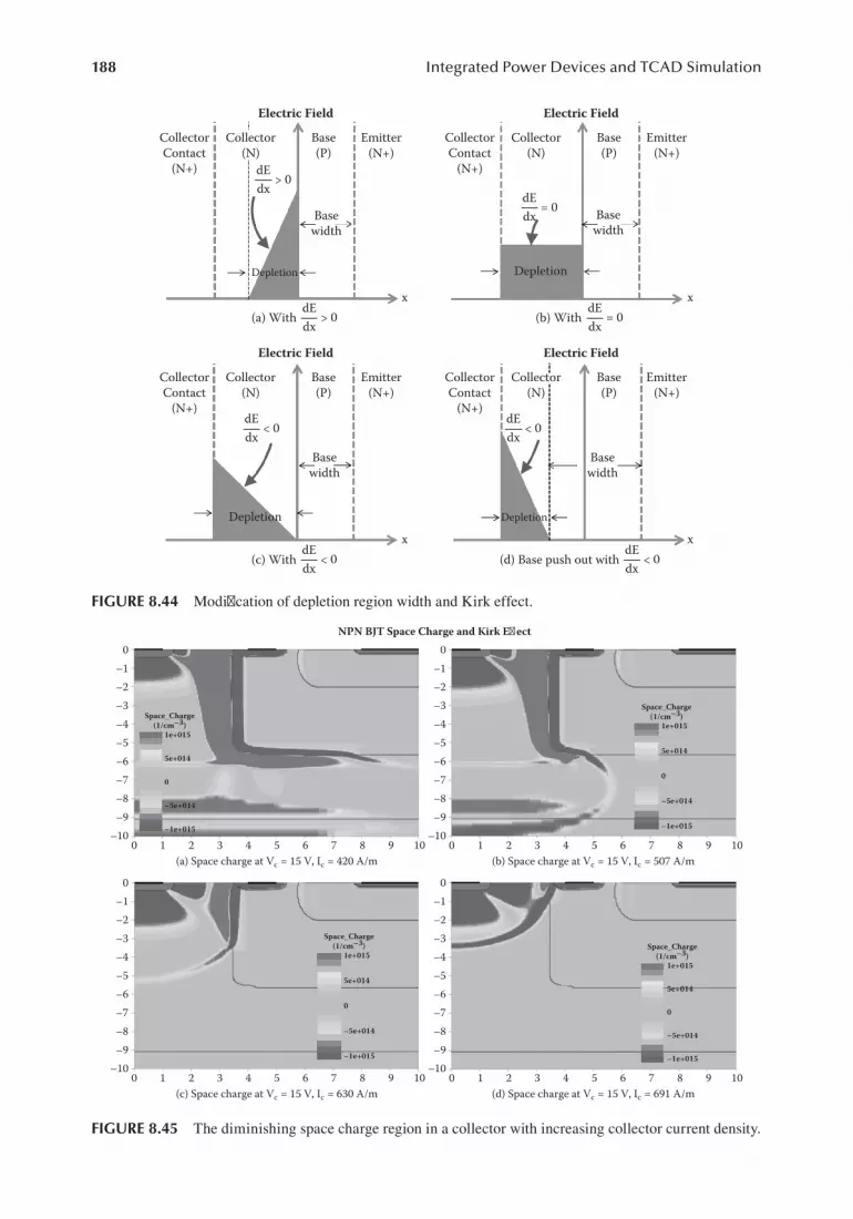
188 Integrated Power Devices and TCAD Simulation
–1–2–3–4–5–6–7–8–9
–10
0
1e+015
Space_Charge(1/cm–3)
5e+014
0
–5e+014
–1e+015
(a) Space charge at Vc = 15 V, Ic = 420 A/m0 1 2 3 4 5 6 7 8 109
–1–2–3–4–5–6–7–8–9
–10
0NPN BJT Space Charge and Kirk Eect
1e+015
Space_Charge(1/cm–3)
5e+014
0
–5e+014
–1e+015
(b) Space charge at Vc = 15 V, Ic = 507 A/m0 1 2 3 4 5 6 7 8 109
–1–2–3–4–5–6–7–8–9
–10
0
1e+015
Space_Charge(1/cm–3)
5e+014
0
–5e+014
–1e+015
(c) Space charge at Vc = 15 V, Ic = 630 A/m0 1 2 3 4 5 6 7 8 109
–1–2–3–4–5–6–7–8–9
–10
0
1e+015
Space_Charge(1/cm–3)
5e+014
0
–5e+014
–1e+015
(d) Space charge at Vc = 15 V, Ic = 691 A/m0 1 2 3 4 5 6 7 8 109
FIGURE 8.45 The diminishing space charge region in a collector with increasing collector current density.
dE(a) With dx
> 0dE
(b) With dx= 0
dE(c) With dx
< 0dE
(d) Base push out with dx< 0
Electric Field
Base(P)
Emitter(N+)
Collector(N)
dEdx
> 0
Basewidth
Depletion
CollectorContact
(N+)
Electric Field
Base(P)
Emitter(N+)
Collector(N)
CollectorContact
(N+)
Electric Field
Base(P)
Emitter(N+)
Collector(N)
CollectorContact
(N+)
Electric Field
Base(P)
Emitter(N+)
Collector(N)
CollectorContact
(N+)
dEdx
= 0 Basewidth
Depletion
dEdx
< 0
Basewidth
Depletion
dEdx
< 0
Basewidth
Depletionx
x
x
x
FIGURE 8.44 Modification of depletion region width and Kirk effect.

189Integrated Power Semiconductor Devices with TCAD Simulation
Suppose a BJT is biased at a forward active region with high collector-emitter current flow. The device is locally heated up by this current. Due to bipolar action, higher temperature causes a higher generation and recombination rate and thus induces an even higher current level, which leads to a positive feedback at some local “hot spots” of the device. This positive temperature and current feedback phenomenon is called thermal runaway and can lead to a catastrophic device failure called second breakdown.
Second breakdown is of course undesirable, and proper design is necessary to minimize this problem. TCAD simulation is done to mimic the thermal runaway and second breakdown and to provide some physical insights during the second breakdown. To be more realistic, heat sink is con-nected to the contacts through thermal resistors (Rth); a schematic of the thermal simulation setup is shown in Figure 8.46.
For this simulation, a 2D simulation is performed so currents are in A/m and power flows are in W/m. Thus, the thermal conductance Rth
−( )1 has units of (W/m)/K rather than W/K. The missing z-depth is omitted. Here, we assume that a thermal conductance of 60 (W/m)/K connects every contacts of the BJT (Figure 8.46) to a heat sink with a constant temperature of 298 K. The BJT base current is first ramped up to 1E-4 A/m, and then the collector voltage is increased to 60 V while the emitter is grounded. Finally, the collector current is ramped up to a high value (about 4200 A/m). From the I-V curve in Figure 8.47, we noticed that breakdown happens at about 65 V but that voltage still increases beyond this point due to internal resistance. After about 75 V is reached, a current snapback takes place: the collector current increases while the voltage decreases. At such high current levels, thermal instability happens, and the device is virtually destroyed. Illustrated in Figure 8.47 are the simulated I-V curves (in linear and log scales) with the self-heating model turned on.
The maximum lattice temperature in the simulated BJT is plotted versus collector voltage and current in Figure 8.48. When the self-heating model is turned off (Figure 8.49), we see a much smaller snapback effect, which highlights the importance of self-heating when simulating high-power devices. With the self-heating model turned on, the temperature rises rapidly after 600 K (327°C): even though the temperature reaches 1400 K in the simulation, a real device would have been destroyed well below this temperature. Readers should also keep in mind that devices are often destroyed by a few hot spots that have been subjected to positive feedback.
This behavior also explains why it is difficult to connect power BJTs in parallel. Since it is almost impossible to make the resistivity of the current paths exactly the same among devices connected in parallel, the one with lowest resistivity will always carry the highest current load and will be more
Base
Heat Sink @ 298 K
NBL/Collector
Rth Rth Rth
Collector Emitter
FIGURE 8.46 Schematic of thermal simulation setup.

190 Integrated Power Devices and TCAD Simulation
1,400.01,200.01,000.0
800.0600.0400.0200.0
0.0
1,600.01,400.01,200.01,000.0
800.0600.0400.0200.0
0.0
1,600.0
Collector Voltage (V) Collector Current (A/m)(a) Temperature vs. collector voltage
Tem
pera
ture
(K)
Tem
pera
ture
(K)Temperature vs. collector voltage
Temperature vs. collector current
(b) Temperature vs. collector current
Temperature vs. Collector CurrentTemperature vs. Collector Voltage
0 10 20 30 40 50 60 80 1E–3 1E–2 1E–1 1E+0 1E+1 1E+2 1E+3 1E+470
FIGURE 8.48 BJT maximum lattice temperature is plotted against (a) collector voltage and (b) collector current.
1000
100
10
1
0.1
0.01
1E–30 10 20 30 40
Collector Voltage Vc (V)
With lattice self-heating modelWith constant temperature (300K)
Colle
ctor
Cur
rent
(A/m
)
50 60 70 80
FIGURE 8.49 With lattice self-heating model turned on, snapback effect is more pronounced than with constant temperature.
3500
3000
2500
2000
1500
1000
500
0
4000
4500
1000
100
10
1
0.01
0.1
0.001
0.0001
10000
Collector Voltage (V) Collector Voltage (V)(a) ermal runaway I-V curve for BJT in linear scale
Colle
ctor
Cur
rent
(A/m
)
Colle
ctor
Cur
rent
(A/m
)
Collector current with self-heatingCollector current with self-heating
(b) ermal runaway I-V curve for BJT in log scale
ermal Runaway I-V Curve Log Scaleermal Runaway I-V Curve Linear Scale
0 10 20 30 40 50 60 8070 0 10 20 30 40 50 60 8070
FIGURE 8.47 I-V curves (a) linear scale and (b) log scale of thermal runaway simulation.

191Integrated Power Semiconductor Devices with TCAD Simulation
likely to suffer thermal runaway as it is subject to higher temperatures. For this reason, unipolar devices such as an LDMOS are preferred when connecting power devices in parallel since carrier mobility degradation at elevated temperatures causes a negative temperature-current feedback loop instead of a positive one.
Figure 8.50 is a collection of plots showing the lattice temperature and current magnitude at dif-ferent points of the I-V curve in Figure 8.47a. Figures 8.50a and 8.50b plot the lattice temperature
Collector Base Emitter
Lattice Temperture (K)298.023298.023298.022298.021298.02298.019298.018298.017298.016298.015298.014
Total Curr. Mag (A/cm2)5
4
3
2
1
0
Total Curr. Mag (A/cm2)50000450004000035000300002500020000150001000050000
Total Curr. Mag (A/cm2)300000
250000
200000
150000
100000
50000
0
1098765432109876543210
1098765432109876543210
1098765432109876543210
0
–1
–2
–3
–4
–5
–6
–7
–8
–9
–10
0
–1
–2
–3
–4
–5
–6
–7
–8
–9
–10
0
–1
–2
–3
–4
–5
–6
–7
–8
–9
–10
0
–1
–2
–3
–4
–5
–6
–7
–8
–9
–10
0
–1
–2
–3
–4
–5
–6
–7
–8
–9
–10
0
–1
–2
–3
–4
–5
–6
–7
–8
–9
–10
Lattice Temperature (K)553.516540520500480460440420419.773
Lattice Temperature (K)1300
1200
1100
1000
900
800
700
NPN BJT ermal Runaway and 2nd Breakdown
Collector Base Emitter
Collector Base Emitter Collector Base Emitter
Collector Base Emitter Collector Base Emitter
(e) Lattice temperature (after thermal runaway) (f ) Total current (after thermal runaway)
(c) Lattice temperature (after 1st snapback) (d) Total current (after 1st snapback)
(a) Lattice temperature (before 1st snapback) (b) Total current (before 1st snapback)
FIGURE 8.50 Lattice temperature and current magnitude plots under different collector voltage, collector current, and temperatures.

192 Integrated Power Devices and TCAD Simulation
and total current before the first snapback (60 V), at room temperature (298 K), and with low cur-rent magnitude. Figures 8.50c and 8.50d are at the location after first snapback (Vc = 36 V), with elevated maximum temperature (550 K) and current magnitude. Figures 8.50e and 8.50f are located after the device’s second breakdown and thermal runaway. At a very high simulated temperature (1400 K), this device should already have been destroyed; the current magnitude is also very high with relatively low collector voltage (22 V).
8.2.6 BJt smAll signAl model And cutoFF FreQuency simulAtion
A small signal model is useful for analog and power IC design. Unlike a power BJT that works in switching mode (saturation and off region), an analog BJT usually works as an amplifier (active region) and is used to amplify small AC signals. If we regard the NPN BJT as a two-port network with a grounded emitter, the base as the input, and the collector as the output, we can draw a simple small signal model for a BJT, as seen in Figure 8.51.
I I e I ec s
V
Vs
V
VBE
t
BE
t= ⋅ −
≈ ⋅
1 when VBE is not close to 0 (8.29)
When a small AC signal VBE is applied to base emitter junction, a collector current gmVBE is cre-ated where gm is called the transconductance and can be expressed as [167]:
gdI
dVd
dVI e
I eV
IV
ImV K
mc
BE BEs
V
V s
V
V
t
c
t
cBE
t
BE
t
= = ⋅
= ⋅ = =
26 (@300 ) (8.30)
This is a simple and yet very useful equation. The input resistance is calculated using
1 1r
dIdV
dIdV
gB
BE
c
BE
m= =β
=βπ
(8.31)
and the input capacitance is expressed as
CdQdV
ddV
I gF
BE BEF c F m= = τ = τπ (8.32)
where τF is the forward transit time that can be viewed as the delay created as carriers travel from collector to emitter. To complete the model, a junction capacitance CJBE needs to be added in paral-lel with the diffusion capacitance previously defined.
C g CF m JBE= τ +π (8.33)
Base (B)
Emitter (E)
Ib
+
–
VBE
+
–
VCE
Collector (C)
Emitter (E)
Ic
Cπ rπ
FIGURE 8.51 Simple small signal model for BJT.

193Integrated Power Semiconductor Devices with TCAD Simulation
A forward-biased base-emitter junction usually has a very small junction capacitance. So it is safe to omit the junction capacitance at this time.
8.2.6.1 Cutoff FrequencyThe cutoff frequency is defined as the frequency at which the AC current gain i iac c bβ = ( / ) falls to unity. It is related to τF as [167]:
1
2 ( )
12
f C VI
t
FJBE t
c
F
=π τ +
≈πτ
(8.34)
Since for a forward-biased base-emitter PN junction, the junction capacitance is quite small, the cutoff frequency expression can be simplified and is approximately inversely proportional to forward transit time τF. Since τF can be measured only in experiment, ft provides a useful way to calculate τF.
The cutoff frequency ft and AC current gain are simulated under different collector current Ic levels, as shown in Figure 8.52. With a fixed collector to emitter voltage 1 VVCE = , VBE is increased from 0.6 V to 1.0 V, and Ic varies accordingly. Intuitively, we may think that with increasing Ic, forward transit time will be smaller and ft will increase. In fact, this relationship is valid only for smaller Ic values. With high collector current, the base width is increased due to the Kirk effect, which increases the base transit time and thus the total forward transit time τF. ft is observed to drop after reaching a maximum value. Designers tend to bias BJT at the peak of ft to achieve better high-frequency results.
8.3 LDMOS
An LDMOS transistor is one of the most important power devices in power ICs. Most of the design efforts in power IC technology are concentrated on how to improve the performance of LDMOS devices. Like a vertical double-diffused MOS (VDMOS) transistor, the channel region is created by the difference between diffusions of body and source N+ (or P+) implants. This is a self-aligned process so that large lithographic feature sizes can be tolerated. Unlike a VDMOS where the silicon epi-layer is used as drain-drift region and a heavily doped substrate is used as drain contact, an
Vce = 1 V, Vbe = 0.6 V, Ic = 0.01 A/m
Vce = 1 V, Vbe = 0.9 V, Ic = 180 A/mVce = 1 V, Vbe = 1.0 V, Ic = 592 A/m
Vce = 1 V, Vbe = 0.8 V, Ic = 18 A/mVce = 1 V, Vbe = 0.7 V, Ic = 0.46 A/m
1.E+3
1.E+2
1.E+1
1.E+01.0 2.0 3.0 4.0
Frequency (Log)
AC
Curr
ent R
atio
(ic/
ib)
5.0 6.0 7.0 8.0
FIGURE 8.52 AC current gain and cutoff frequency comparison under a different collector current.

194 Integrated Power Devices and TCAD Simulation
LDMOS drain contact is at the silicon surface (same side as source and body). For DMOS, lateral or vertical indicates whether current flows laterally or vertically from drain contact to source/body contact.
A well-designed LDMOS should have a high breakdown voltage, low on-state resistance, and a small gate to drain capacitance. This section focuses mostly on how to use a TCAD tool to improve the device breakdown voltage without jeopardizing the on-resistance.
For 0.35 µm technology or above, LOCOS (LOCal Oxidation of Silicon) is usually the isola-tion technology of choice. As power ICs move toward smaller feature sizes, STI is also becoming popular. In this section, we limit ourselves to LDMOS using STI technology to reflect this trend.
Eight examples of LDMOS (I to VIII), with slightly different structures, are first discussed. The section examines in detail electric field distribution and how to optimize various doping concentra-tions to improve the breakdown voltage and reduce on-resistance. For power IC applications, the breakdown voltage requirements for LDMOS range from 20 to 1000 V; power ICs that can sustain over 300 V are generally referred to as high-voltage IC (HVIC). They are usually used in applica-tions that require high voltage but low current. In this section, LDMOS with breakdown voltage less than 150 V is discussed.
8.3.1 BreAkdown voltAge improvement
This section presents the LDMOS in a step-by-step fashion. Eight different LDMOS structures are introduced, with a focus on how to use TCAD tools to improve the breakdown voltage and reduce the on-state resistance.
8.3.1.1 Basic LDMOS Structure with N-Type Epitaxial Layer (LDMOS I)LDMOS with a breakdown voltage less than 150 V are popular for power ICs in consumer elec-tronics and transportation applications. A standard LDMOS structure without STI in the drain-drift region is introduced first. A schematic representation of an LDMOS with an N-type epitaxial layer (or an N-well) is illustrated in Figure 8.53a. The simulation cell pitch for this LDMOS is set to be 10 µm with a depth of 20 µm. (To get a larger view, the depth of plotted structures is truncated to 10 µm, but the simulation size is 20 µm deep.) The source and body terminals are connected together for enhanced breakdown capability. The poly gate is 0.4 µm thick by 2 µm long, is phosphorus-doped at 1E + 19 cm−3, extends over the P-body region, and covers part of the drain-drift region. Since electrons accumulate underneath the gate when a positive voltage is applied to that electrode, this extension may help reduce the on-resistance. The gate oxide thick-ness is chosen to be 200 Å to reach an appropriate threshold voltage while maintaining oxide robustness under high gate voltages. The channel length is about 0.8 µm. The total drain length (measured from P-body edge to device right edge) is about 7.5 µm. The P-body has a depth of about 2.75 µm. The N+ and P+ regions (NSD and PSD) each have a width of 0.75 µm; no substrate contact is included in this structure.
Figure 8.53 also illustrates some results from TCAD simulation. Figure 8.53b is the material plot. Three materials—silicon, polysilicon, and oxide—are included in this simulation. Please note that in the simulation contacts are simply boundary conditions and not a type of material; thus, they are plotted for illustration purposes only. The net doping is shown in Figure 8.53c, and Figure 8.53d is the surface plot (with absolute value) of the net doping.
For this simple LDMOS structure, we use N-epi with constant doping as the drain. Suppose we want to design an LDMOS with breakdown voltage greater than 100 V. We can start by checking the single-sided parallel plane breakdown voltage listed in Table 6.6. As a starting point, an N-epi layer doping concentration of 5E + 15 cm−3 may be appropriate, since it has a P+/N breakdown volt-age close to 100 V. The N-epi layer will act as the drain-drift region, which will support most of the breakdown voltage. (Part of the breakdown voltage is supported within P-body due to graded junction.) The simulation parameters are listed in Table 8.6.

195Integrated Power Semiconductor Devices with TCAD Simulation
The breakdown simulation is performed with source/body contact and gate contact grounded while the potential at the drain contact is increased until leakage current increases rapidly (ava-lanche breakdown). The substrate contact is not included in this simulation. The simulation results after device breakdown are shown in Figure 8.54. From Figure 8.54a we see the equipotential lines after breakdown extend primarily within the N-epi region, which means that the N-epi supports most of the voltage applied to the drain. Unfortunately, the simulated breakdown voltage is found
Source/Body
Source/Body
Source/Body
GateGateDrain
Drain
DrainNet_Doping19
15
10
5
0
–5
–10
–15
–18.9998
Net_Doping19
1816141210
8642
–1–2–3
18.5
18
17.5
17
16.5
16
15.5
15
N+N+P+
P-body
P-body
P-body Junction LineContact
Boundary
FEM_StructurePolySiO2Si
109876543210–10
–9
–8
–7
–6
–5
–4
–3
–2
–1
0
–10
–9
–8
–7
–6
–5
–4
–3
–2
–1
0
109876543210
Poly Gate
Gate
N-epi or N-well
(a) Schematic view
LDMOS with N-epi (LDMOS I)
(b) Material plot
(c) Net doping plot (d) Surface plot of net doping
N-epi
Net_Doping
N-epi
N-epi
DrainSource/body
FIGURE 8.53 Schematic reprentation of an LDMOS with N-epi.
TABLE 8.6Simulation Parameters for LDMOS I
Parameters for Simulation Value
X range 0 to 10 µm
Y range 0 to −20 µm
N-epi 5E + 15 cm−3
P-body max concentration 2E + 17 cm−3
P-body location (x1, x2, dx1, dx2) Gaussian X = (0, 1.5, 0.35, 0.35); y = (−0.6, −0.6, 0.8, 0.8)
Oxide thickness 200 Å
Poly gate thickness 0.4 µm
Poly gate length 2 µm
Poly gate doping Phosphorus, 1E + 19 cm−3
Channel length 0.8 µm (approx.)
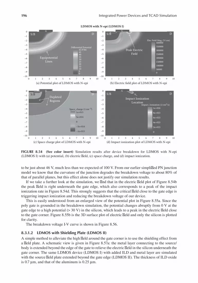
196 Integrated Power Devices and TCAD Simulation
to be just about 46 V, much less than we expected of 100 V. From our earlier simplified PN junction model we know that the curvature of the junction degrades the breakdown voltage to about 80% of that of parallel planes, but this effect alone does not justify our simulation results.
If we take a further look at the simulation, we find that in the electric field plot of Figure 8.54b the peak field is right underneath the gate edge, which also corresponds to a peak of the impact ionization rate in Figure 8.54d. This strongly suggests that the critical field close to the gate edge is triggering impact ionization and reducing the breakdown voltage of our device.
This is easily understood from an enlarged view of the potential plot in Figure 8.55a. Since the poly gate is grounded in the breakdown simulation, the potential changes abruptly from 0 V at the gate edge to a high potential (> 30 V) in the silicon, which leads to a peak in the electric field close to the gate corner. Figure 8.55b is the 3D surface plot of electric field and only the silicon is plotted for clarity.
The breakdown voltage I-V curve is shown in Figure 8.56.
8.3.1.2 LDMOS with Shielding Plate (LDMOS II)A simple method to alleviate the high field around the gate corner is to use the shielding effect from a field plate. A schematic view is given in Figure 8.57a: the metal layer connecting to the source/body is extended beyond the edge of the gate to relieve the electric field in the silicon underneath the gate corner. The same LDMOS device (LDMOS I) with added ILD and metal layer are simulated with the source field plate extended beyond the gate edge (LDMOS II). The thickness of ILD oxide is 0.7 µm, and that of the aluminum is 0.25 µm.
LDMOS with N-epi (LDMOS I)
(a) Potential plot of LDMOS with N-epi (b) Electric field plot of LDMOS with N-epi
(c) Space charge plot of LDMOS with N-epi (d) Impact ionization plot of LDMOS with N-epi
DD
Peak ElectricField
EquipotentialLines
DepletedRegions
GS/B
DImpact Ionization
LocationImpact_Ionization (1/cm3/s)
Space_charge (1/cm–3) 1e+024
8e+023
6e+023
4e+023
2e+023
0
Elec Field Mag. (V/cm)400000350000300000250000200000
100000150000
500000
Differential Potential45.978445
3540
302520
1015
50
1e+015
5e+014
0
–5e+014
–1e+015
GS/B
GS/B
DG
S/B
109876543210
0
–1
–2
–3
–4
–5
–6
–7
–8
–9
–10
109876543210
0
–1
–2
–3
–4
–5
–6
–7
–8
–9
–10
109876543210
0
–1
–2
–3
–4
–5
–6
–7
–8
–9
–10
109876543210
0
–1
–2
–3
–4
–5
–6
–7
–8
–9
–10
FIGURE 8.54 (See color insert) Simulation results after device breakdown for LDMOS with N-epi (LDMOS I) with (a) potential, (b) electric field, (c) space charge, and (d) impact ionization.

197Integrated Power Semiconductor Devices with TCAD Simulation
Figure 8.57b shows the simulated result of a material plot. Four materials are used—silicon, poly-silicon (poly), SiO2 (oxide), and aluminum (al)—with aluminum metal plate extending over the gate. The length of the metal gate will affect the breakdown voltage, which is discussed later. A field plate length of 6 µm (measured from the simulation edge) was chosen as a starting point. Figures 8.57c and 8.57d are an the net doping plots. The simulation parameters are listed in Table 8.7.
A breakdown simulation is performed by applying a high voltage on the drain while keeping the source/body and gate contacts grounded. Figure 8.58 shows the simulation results after device breakdown. (Silicon area below Y = −10 µm is truncated for enlarged view, since that area has little information of interest.) The equipotential lines illustrated in Figure 8.58a show a dramatic improvement compared with those of LDMOS I in Figure 8.54a: the field plate has successfully extended the equipotential lines (Figure 8.58b), and we also see evidence of an increased depletion width in Figure 8.58c. With the field plate, the peak electric field has been successfully shifted away from the gate edge and into the oxide ILD; oxide has a much higher (> 10x) critical electric field than silicon, so it is unlikely to provoke the avalanche effect. Additionally, the impact ionization (Figure 8.58d) now mostly takes place at the PN junction in the bulk rather than at the surface. With
Elec Field Mag. (V/cm)
Elec
Fie
ld M
ag. (
V/cm
)High Potential in Silicon 350000300000250000200000150000100000
50000
–1–2–3
–6–5–4
–7–8
–9 1 23 4
5x(micron)6
7 8 9 10
Drain
N-epi
P-body
S/B
0 Volt at the gate edge
Differential Potential45.9784454035302520151050
0.5–4.5
–4–3.5
–3–2.5
–2–1.5
–1–0.5
0
1 1.5 2 2.5 3 3.5 4 4.5
400000
350000
300000
250000
200000
150000
100000
50000
0
(b) 3D surface plot of electric field(a) Enlarged potential plot at the gate edge
LDMOS with N-epi (LDMOS I)
y(micron)
FIGURE 8.55 (a) Enlarged potential plot and (b) 3D electric field surface plot of LDMOS with N-epi (LDMOS I).
1E+11E+01E–11E–21E–31E–41E–51E–61E–71E–81E–9
1E–101E–111E–12
Breakdown Voltage of LDMOS I
0 5 10 15 20 25Drain Voltage (V)
Dra
in C
urre
nt (A
/m)
30 35 40 45 50
FIGURE 8.56 Breakdown voltage I-V plot of the simple LDMOS (LDMOS I).

198 Integrated Power Devices and TCAD Simulation
the addition of the field plate, the breakdown voltage has been increased from 47 V to 89 V, but we are still shy of our design goal of 100 V.
The surface plot of an electric field for LDMOS II is shown in Figure 8.59 compared with LDMOS I. With a field plate, a second peak is observed at the PN junction in the silicon bulk. As in previous surface plots for LDMOS I, the electric field is shown only in the silicon material, and Y range is from −10 µm to 0 µm.
Source/Body
Source/body
Source/body Source/body
Field PlateGate
Drain
Drain Drain
DrainNet_Doping
19
15
10
5
0
–5
–10
–15
–18.9998
Net_Doping19
1816141210
8642
–1–2–3
18.5
18
17.5
17
16.5
16
15.5
15
N+N+P+
P-body
P-body
P-body
Junction Line
ContactBoundaryField Plate
FEM_Structure
Polyal(xlam = 0.55)SiO2
Si
109876543210–10
–9
–8
–7
–6
–5
–4
–3
–2
–1
0
–10
–9
–8
–7
–6
–5
–4
–3
–2
–1
0
109876543210
Poly Gate ILD
N-epi or N-well
(a) Schematic view
LDMOS with Field Plate (LDMOS II)
(b) Material plot
(c) Net doping plot (d) Surface plot of net doping
N-epi
Net_Doping
N-epi
N-epi
DrainSource/body
FIGURE 8.57 LDMOS structure with field plate (LDMOS II).
TABLE 8.7Simulation Parameters for LDMOS with Field Plate
Parameters for Simulation Value
X range 0 to 10 µm
Y range 0 to −20 µm
N-epi 5E + 15 cm−3
P-body max concentration 2E + 17 cm−3
P-body location (x1, x2, dx1, dx2) Gaussian X = (0, 1.5, 0.35, 0.35); y = (−0.6, −0.6, 0.8, 0.8)
Oxide thickness 200 Å
Poly gate thickness 0.4 µm
Poly gate length 2 µm
Channel length 0.8 µm (approx.)
Interlayer dielectric thickness 0.7 µm
Source metal shield plate length 6 µm (from source) or 2.5 µm (from gate edge)

199Integrated Power Semiconductor Devices with TCAD Simulation
LDMOS with Field Plate (LDMOS II)
(a) Potential plot of LDMOS II (b) Electric field plot of LDMOS II
(c) Space charge plot of LDMOS II (d) Impact ionization plot of LDMOS II
DD
High ElectricField
EquipotentialLines
Field PlateField Plate
DepletedRegions
G
S/B
DImpact Ionization
Location
Impact_Ionization (1/cm3/s)Space_charge (1/cm–3) 1e+024
8e+0236e+0234e+0232e+0230
Elec Field Mag.(V/cm)
400000350000300000250000200000
100000150000
500000
Differential Potential88.671180
6070
504030
1020
0
1e+0155e+0140–5e+014–1e+015
G
S/B
GS/B
DG
S/B
109876543210
0
–1
–2
–3
–4
–5
–6
–7
–8
–9
–10
109876543210
0
–1
–2
–3
–4
–5
–6
–7
–8
–9
–10
109876543210
0
–1
–2
–3
–4
–5
–6
–7
–8
–9
–10
109876543210
0
–1
–2
–3
–4
–5
–6
–7
–8
–9
–10
FIGURE 8.58 (See color insert) Simulation results after device breakdown for LDMOS with N-epi and field plate (LDMOS II) with (a) potential, (b) electric field, (c) space charge, and (d) impact ionization.
Elec Field Mag. (V/cm)
Elec
Fie
ld M
ag. (
V/cm
)
350000400000
300000250000200000150000100000
50000
–1–2
–3
–6–5
–4
–7–8
–9 12
34
5x(micron)
67
89
10
Drain
N-epi
P-body
S/B
400000
350000
300000
250000
200000
150000
100000
50000
0
y(micron)
FIGURE 8.59 Surface plot of electric field of LDMOS II.

200 Integrated Power Devices and TCAD Simulation
Different field plate lengths will change the breakdown voltage, so a proper design is necessary to ensure optimal results. The breakdown voltage variation with different field plate lengths is simu-lated and shown in Figure 8.60. When the field plate is short (e.g., 3 µm measured from the source edge), breakdown voltage is only 61 V; a sharp increase of breakdown voltage is seen when the field shielding plate length is longer than 4 µm because the field plate extends beyond the gate edge, which diverts the peak field into the ILD oxide. With a field plate length of 6 µm, the breakdown voltage increases to 89 V and then saturates; no further increase of breakdown voltage is observed with longer field plates.
Another possible approach for the field plate is to connect it from the drain side (going left) instead of the source side. This is investigated in Figure 8.61, which shows that longer drain field plates are detrimental to the breakdown voltage.
This unusual behavior can be explained by noting that when the field plate is connected to the grounded source, its potential is zero, which flattens out the equipotential lines underneath the plate. However, when the field plate is connected to the drain side, it acquires a high voltage from the drain, which tends to push back the equipotential lines underneath it and makes them more crowded. A comparison of the equipotential lines spacing for source/drain field plates of differ-ent lengths is shown in Figure 8.62. The longer field plate from the source side yields the highest
70
60
65
40
50
55
45
Field Plate Length (from drain) Effect on BV
61 6058
5148
3 4Field Plane Length (from drain in µm)
Brea
kdow
n Vo
ltage
(V)
5 6 7
FIGURE 8.61 Breakdown voltage variation with different field plate lengths from the drain side.
100
90
80
70
60
50
Field Plate Length (from source) Eect on BV
61 61 66
83
89 89
2 3 4Field Plane Length (from source in um)
Brea
kdow
n Vo
ltage
(V)
5 6 7
FIGURE 8.60 Breakdown voltage variation with different field plate lengths from the source side.

201Integrated Power Semiconductor Devices with TCAD Simulation
breakdown value (89 V), while the same plate from the drain side dramatically lowers the break-down voltage to 48 V. Short field plates on either side yield a similar breakdown voltage of 61 V, as shown in Figures 8.62a and 8.62d.
8.3.1.3 LDMOS with STI in the Drain-Drift Region (LDMOS III)A common way to improve breakdown voltage is to divert the peak electric field into the oxide; depending on process technology, either LOCOS or STI is used for this purpose. Since the growing trend is to use STI to replace LOCOS in most process technology below 0.25 µm, we discuss only STI in this section.
The STI trench is located in the drain-drift region but should also have a certain overlap with poly gate. A schematic of our sample structure is shown in Figure 8.63a (LDMOS III) with a mate-rial plot in Figure 8.63b. The oxide trench (STI) is within the drain-drift region with a small overlap with the gate (0.5 µm); an edge slope (3 degree angle) is also used to mimic the real manufactured shape. Net doping plots are given in Figures 8.63c and 8.63d. For a 3D surface plot, Y ranges from −10 µm to 0 µm (the simulated device has a total depth of 20 µm and poly gate is located above 0 µm). The simulation parameters for this LDMOS are listed in Table 8.8.
The simulated equipotential lines at breakdown are shown in Figure 8.64a. The breakdown volt-age of the LDMOS with STI is about 87 V, which is close to the value achieved for LDMOS II
LDMOS with Field Plate (LDMOS II)
(a) Potential plot of LDMOS II with eld plate length = 3 µm from source and BV = 61 V
(b) Potential plot of LDMOS II with eld plate length = 7 µm from source and BV = 89 V
(c) Potential plot of LDMOS II with eld plate length = 7 µm from drain and BV = 48 V
(d) Potential plot of LDMOS II with eld plate length = 3 µm from drain and BV = 61 V
DD
Field plate from right: 7 µmBreakdown voltage: 48 V
Field plate from right: 3 µmBreakdown voltage: 61 V
Field plate from left: 3 µmBreakdown voltage: 61 V
Field plate from left: 7 µmBreakdown voltage: 89 V
G
S/B
D
Dierential Potential60.5599
60
50
40
30
10
20
0
Dierential Potential60.549
60
50
40
30
10
20
0
Dierential Potential47.7741
4045
3035
1015
5
2025
0
Dierential Potential
708090
60504030
1020
0
G
S/B
GS/B
DG
S/B
109876543210
0
–1
–2
–3
–4
–5
–6
–7
–8
–9
–10
109876543210
0
–1
–2
–3
–4
–5
–6
–7
–8
–9
–10
109876543210
0
–1
–2
–3
–4
–5
–6
–7
–8
–9
–10
109876543210
0
–1
–2
–3
–4
–5
–6
–7
–8
–9
–10
FIGURE 8.62 Comparison of equipotential lines for field plates connected from the source side and drain side: (a) 3 µm from the source (left) side; (b) 7 µm from the source (left) side; (c) 7 µm from the drain (right) side; (d) 3 µm from the drain (right) side.
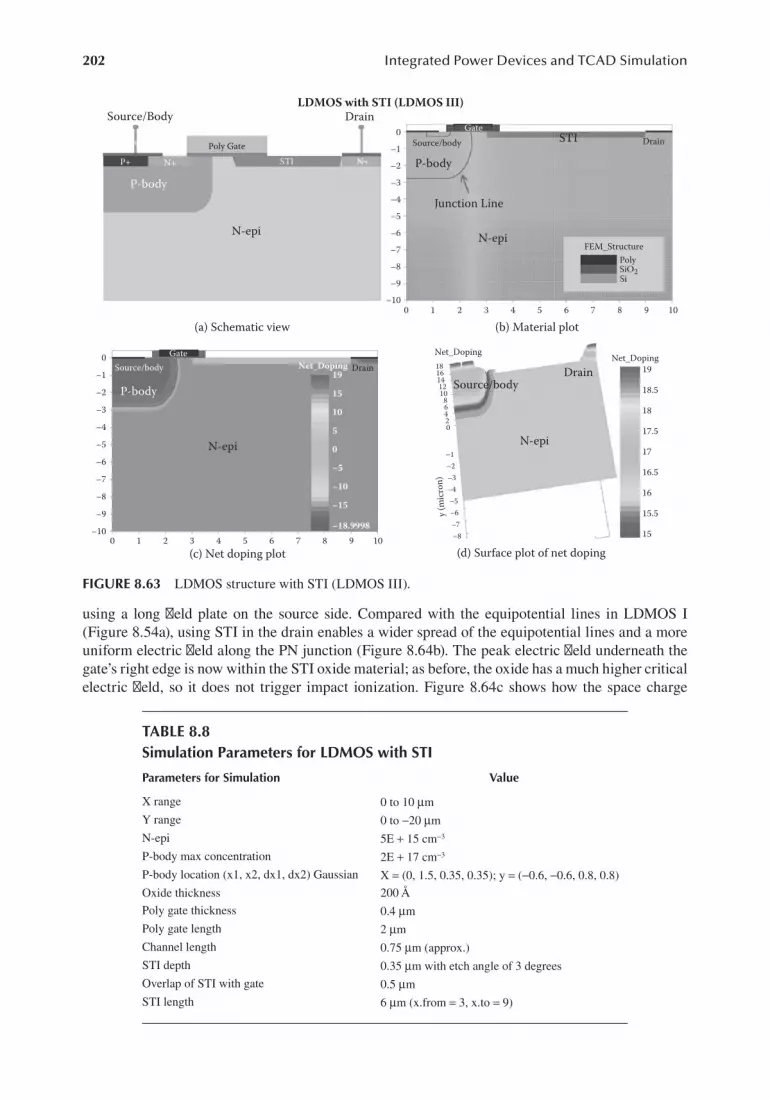
202 Integrated Power Devices and TCAD Simulation
using a long field plate on the source side. Compared with the equipotential lines in LDMOS I (Figure 8.54a), using STI in the drain enables a wider spread of the equipotential lines and a more uniform electric field along the PN junction (Figure 8.64b). The peak electric field underneath the gate’s right edge is now within the STI oxide material; as before, the oxide has a much higher critical electric field, so it does not trigger impact ionization. Figure 8.64c shows how the space charge
Source/Body
Source/bodyGate
Source/body Source/bodyGate
Drain
Drain Drain
DrainNet_Doping19
15
10
5
0
–5
–10
–15
–18.9998
Net_Doping1918
16141210
86420
–1–2–3–4–5–6–7–8
18.5
18
17.5
17
16.5
16
15.5
15
N+N+P+
P-body
P-body
P-body
Junction Line
STI
FEM_StructurePolySiO2Si
109876543210–10
–9
–8
–7
–6
–5
–4
–3
–2
–1
0
–10
–9
–8
–7
–6
–5
–4
–3
–2
–1
0
109876543210
Poly GateSTI
N-epi
(a) Schematic view
LDMOS with STI (LDMOS III)
(b) Material plot
(c) Net doping plot (d) Surface plot of net doping
y (m
icro
n)N-epi
Net_Doping
N-epi
N-epi
DrainSource/body
FIGURE 8.63 LDMOS structure with STI (LDMOS III).
TABLE 8.8Simulation Parameters for LDMOS with STI
Parameters for Simulation Value
X range 0 to 10 µm
Y range 0 to −20 µm
N-epi 5E + 15 cm−3
P-body max concentration 2E + 17 cm−3
P-body location (x1, x2, dx1, dx2) Gaussian X = (0, 1.5, 0.35, 0.35); y = (−0.6, −0.6, 0.8, 0.8)
Oxide thickness 200 Å
Poly gate thickness 0.4 µm
Poly gate length 2 µm
Channel length 0.75 µm (approx.)
STI depth 0.35 µm with etch angle of 3 degrees
Overlap of STI with gate 0.5 µm
STI length 6 µm (x.from = 3, x.to = 9)

203Integrated Power Semiconductor Devices with TCAD Simulation
extends into the drift region. As seen in Figure 8.64d, the region of maximum impact ionization for this structure has been shifted away from the silicon surface and into the bulk of the device.
For a better view of the electric field distribution within the device, a 3D surface plot is shown in Figure 8.65. Compared with the LDMOS I case (Figure 8.55b), the added STI region has increased the electric field in the bulk of the device and the PN junction, making the electric field more uni-form and enabling a higher breakdown voltage.
8.3.1.4 LDMOS with Both STI Oxide and Field Plate (LDMOS IV)The next step of our design is to combine the concepts of LDMOS II (source field plate) and LDMOS III (STI); both seem to increase the breakdown voltage, but neither method on its own has met our design target value of 100 V.
A schematic view of this structure (LDMOS IV) is shown in Figure 8.66a, along with the material plot in Figure 8.66b. The field plate length is 6 µm just as in LDMOS II, while the oxide trench (STI) has the same physical parameters as in LDMOS III. Figures 8.66c and 8.66d illus-trate the net doping plot of LDMOS IV. As with our previous LDMOS structures, the substrate contact is not included. The simulation parameters for our LDMOS IV structure are listed in Table 8.9.
The equipotential lines for this structure are plotted in Figure 8.67a; the breakdown voltage is only 88 V, and no significant improvement is seen over either LDMOS II or III. In fact, both field plate and STI oxide methods employ the same idea of diverting the peak electric field away from silicon at the gate edge and into an oxide layer (either STI oxide or ILD oxide). There seems to be
LDMOS with STI (LDMOS III) at Breakdown
(a) Potential plot of LDMOS with STI (LDMOS III) (b) Electric field of LDMOS with STI (LDMOS III)
(c) Space charge plot of LDMOS III (d) Impact ionization plot of LDMOS III
DD
High ElectricField
EquipotentialLines
DepletedRegions
G
S/B
DImpact Ionization
Location
STISTI
STISTI
BV = 87 V
Impact_Ionization (1/cm3/s)Space_charge (1/cm–3) 1e+024
8e+023
6e+023
4e+023
2e+023
0
Elec Field Mag. (V/cm)400000
350000
300000
250000
200000
100000
150000
50000
0
Differential Potential87.293780
6070
504030
1020
0
1e+015
5e+014
0
–5e+014
–1e+015
G
S/B
G
S/B
DG
S/B
109876543210
0
–1
–2
–3
–4
–5
–6
–7
–8
–9
–10
109876543210
0
–1
–2
–3
–4
–5
–6
–7
–8
–9
–10
109876543210
0
–1
–2
–3
–4
–5
–6
–7
–8
–9
–10
109876543210
0
–1
–2
–3
–4
–5
–6
–7
–8
–9
–10
FIGURE 8.64 (See color insert) Simulation results at device breakdown for LDMOS with N-epi and STI (LDMOS III) with (a) potential, (b) electric field, (c) space charge, and (d) impact ionization.

204 Integrated Power Devices and TCAD Simulation
Elec
Fie
ld M
ag. (
V/cm
)
Elec
Fie
ld M
ag. (
V/cm
)
700000800000
600000500000400000300000200000100000
–1–2
–3
–6–5
–4
–7–8
–9 12
34
5x(m
icron)67
89
10
Drain
N-epi
P-body
S/B
400000
350000
300000
250000
200000
150000
100000
50000
0
y(micron)
FIGURE 8.65 Surface plot of electric field of LDMOS with STI (LDMOS III).
Source/Body
Source/body
Source/body
Source/bodyGate
Gate
Drain
Drain
Drain
DrainNet_Doping
19151050–5–10–15
–18.9998
Net_Doping19
1816141210
86420
–1–2
–3
–4
18.5
18
17.5
17
16.5
16
15.5
15
N+N+P+
P-body
P-body
P-body
Junction Line
STI
FEM_StructurePolySiO2
SiAl(xlam = 0.55)
109876543210–10
–9
–8
–7
–6
–5
–4
–3
–2
–1
0
–10
–9
–8
–7
–6
–5
–4
–3
–2
–1
0
109876543210
Poly GateSTI
ILD
N-epi
(a) Schematic view
LDMOS with STI and Field Plate (LDMOS IV)
(b) Material plot
(c) Net doping plot (d) Surface plot of net doping
N-epi
Net_Doping
N-epi
N-epi
Drain
Source/body
FIGURE 8.66 LDMOS structure with STI and field plate (LDMOS IV).

205Integrated Power Semiconductor Devices with TCAD Simulation
TABLE 8.9Simulation Parameters for LDMOS with STI and Field Plate (LDMOS IV)
Parameters for Simulation Value
X range 0 to 10 µm
Y range 0 to −20 µm
N-epi 5E + 15 cm−3
P-body max concentration 2E + 17 cm−3
P-body location (x1, x2, dx1, dx2) Gaussian X = (0, 1.5, 0.35, 0.35); y = (−0.6, −0.6, 0.8, 0.8)
Oxide thickness 200 Å
Poly gate thickness 0.4 µm
Poly gate length 2 µm
Channel length 0.8 µm (approx.)
STI depth 0.35 µm with etch angle of 3 degrees
Overlap of STI with gate 0.5 µm
STI length 6 µm (x.from = 3, x.to = 9)
Interlayer dielectric thickness 0.7 µm
Source metal shield plate length 6 µm (from source) or 2.5 µm (from gate edge)
LDMOS with STI and Field Plate (LDMOS IV) at Breakdown
(a) Potential plot of LDMOS IV (b) Electric field plot of LDMOS IV
(c) Space charge plot of LDMOS IV (d) Impact ionization plot of LDMOS IV
DD
High ElectricField
Field Plate
EquipotentialLines
DepletedRegions
G
S/B
D
Impact IonizationLocation
STISTI
STISTI
Impact_Ionization (1/cm3/s)Space_charge (1/cm–3) 1e+024
8e+023
6e+023
4e+023
2e+023
0
Elec Field Mag. (V/cm)400000350000300000250000200000
100000150000
500000
Differential Potential88.235280
6070
504030
1020
0
1e+015
5e+014
0
–5e+014
–1e+015
G
S/B
G
S/B
DG
S/B
109876543210
0
–1
–2
–3
–4
–5
–6
–7
–8
–9
–10
109876543210
0
–1
–2
–3
–4
–5
–6
–7
–8
–9
–10
109876543210
0
–1
–2
–3
–4
–5
–6
–7
–8
–9
–10
109876543210
0
–1
–2
–3
–4
–5
–6
–7
–8
–9
–10
FIGURE 8.67 (See color insert) Simulation results after device breakdown for LDMOS with STI and field plate (LDMOS IV) with (a) potential, (b) electric field, (c) space charge, and (d) impact ionization.

206 Integrated Power Devices and TCAD Simulation
a limit to this idea, so thinking outside the box is required to get further improvements. As usual, Figure 8.67b shows the electric field distribution, which is similar to that of LDMOS II and LDMOS III: electric field peaks in the oxide; and increased electric field levels in the silicon bulk at the PN junction. Figure 8.67c is the space charge plot, and Figure 8.67d is the impact ionization plot. The latter happens at the same location as LDMOS II and LDMOS III: as before, moving the impact ionization away from the surface has the added benefit of lowering the gate oxide stress and improv-ing the long-term reliability of the oxide.
The surface plot of the electric field for LDMOS IV is shown in Figure 8.68. We note the simi-larities between LDMOS II, III, and IV in terms of the electric field distribution within the device.
8.3.1.5 LDMOS with RESURF from P-epi Layer (LDMOS V)We previously observed that diverting the peak electric field from the silicon to the oxide is effec-tive in improving the breakdown voltage. Unfortunately, the breakdown voltage we achieved is still below our target value of 100 V. In fact, a basic rule of thumb in the power semiconductor industry is to design with a 20 to 30% safety margin in breakdown voltage to account for device fabrication tolerance and long-term degradation. So for a 100 V design we actually need at least 120 to 130 V of breakdown voltage.
If we take a look at the 3D electric field surface plots of all the LDMOS that we have discussed so far, they all feature a triangular-shaped field close to the source/body region, so a large portion of silicon that can support the drain voltage is wasted. From Poisson’s equation, we can associate the breakdown voltage with the volume under the 3D surface plots of the electric field: a larger volume leads to higher breakdown voltage. Unfortunately, a critical electric field limits how high the electric field level can go. Therefore, the only way to increase the breakdown voltage is to make the surface electric field as uniform as possible so that this peak value can contribute to the integral over a wider range.
To achieve this, we can employ the concept we explored for the PN junction diode with NBL. In that device, the breakdown voltage was greatly improved when merging the depleted regions of the N-region with that of the NBL; the potential gained by of the NBL further depletes the silicon
Elec
Fie
ld M
ag. (
V/cm
)
Elec
Fie
ld M
ag. (
V/cm
)
500000
600000
400000
300000
200000
100000
–1–2
–3
–6–5
–4
–7–8
–9 12
34
5x(micron)6
78
910
Drain
N-Epi
P-body
S/B
700000
600000
500000
400000
200000
300000
100000
0y(micron)
FIGURE 8.68 Surface plot of electric field of LDMOS IV.

207Integrated Power Semiconductor Devices with TCAD Simulation
area above and below, creating a more uniform distribution of electric field. If we take a look at our LDMOS, we find that we can create a similar effect: since we are using an N-epi (or N-well) rather than P-epi (or P-well), a PBL (P-type buried layer) could be used under the P-body so that the interac-tion of the P-body and PBL depletion regions creates a similar effect as a PN junction diode with NBL.
However, in real manufacturing P-epi is more prevalent than N-epi, and the drain-drift region is created by implantation and diffusion of an N-well. The P-body is typically connected with P-epi in many LDMOS designs: this means the P-epi region under the N-well can gain a low potential from either a grounded substrate or the P-body. We now choose to adjust our design; instead of using PBL, P-epi is used to further deplete an N-well located above it. Our new structure will be called an LDMOS with P-epi (LDMOS V), a schematic of which is given in Figure 8.69a.
Figure 8.69b is the material plot of LDMOS V with added junction lines. For this device struc-ture, we include the same field plate in the simulation as that of LDMOS II (6 µm from the source side), but we do not include the STI from LDMOS III. From the net doping plot of Figures 8.69c and 8.69d we can see the connection between P-body and P-epi.
Table 8.10 lists the simulation parameters of LDMOS V. In this design, doping concentration in the P-epi is chosen to be 1E + 15 cm−3, and the N-well has a doping concentration of 5E + 15 cm−3, the same doping concentration as the N-epi we previously used; all other parameters are kept the same.
The simulation is performed with source/body and gate contacts grounded, while the drain volt-age increased until breakdown. With the same N-well doping of 5E + 15 cm−3 as before, the break-down voltage now increases by more than 50% to a value of 147 V. Figure 8.70a is the potential plot, which shows good spacing of the equipotential lines, while the electric field plot is given in
Source/Body
Source/body
Source/body Source/bodyGate
Gate
Drain
DrainDrain
DrainNet_Doping
19
15
10
5
0
–5
–10
–15
–19
Net_Doping19
1816141210
86420
–1–2–3–4–5
18
17
16
14
15
N+N+P+P-body
P-body
P-body
Junction Line
FEM_StructureSiO2Al(xlam = 0.55)PolySi
109876543210–10
–9
–8
–7
–6
–5
–4
–3
–2
–1
0
–10
–9
–8
–7
–6
–5
–4
–3
–2
–1
0
109876543210
Poly Gate ILD
P-epi
(a) Schematic view
LDMOS with RESURF from P-epi (LDMOS V)
(b) Material plot
(c) Net doping plot (d) Surface plot of net doping
y (micron)
P-epi
Net_Doping
P-epi
P-epi
N-well
N-well
N-well
N-well
Drain
Source/body
FIGURE 8.69 LDMOS structure with P-epi (LDMOS V).

208 Integrated Power Devices and TCAD Simulation
TABLE 8.10Simulation Parameters for LDMOS with Field Plate and P-epi RESURF (LDMOS V)
Parameters for Simulation Value
X range 0 to 10 µm
Y range 0 to −20 µm
P-epi 1E + 15 cm−3
P-body max concentration 2E + 17 cm−3
P-body location (x1, x2, dx1, dx2) Gaussian x = (0, 1.5, 0.35, 0.35); y = (−0.6, −0.6, 0.8, 0.8)
N-well max concentration 5E + 15 cm−3
N-well location (x1, x2, dx1, dx2) Gaussian x = (2, 10, 0.25, 0.25); y = (−6, 0, 0.25, 0.25)
Oxide thickness 200 Å
Poly gate thickness 0.4 µm
Poly gate length 2 µm
Channel length 0.8 µm (approx.)
Interlayer dielectric thickness 0.7 µm
Source metal shield plate length 6 µm (from source) or 2.5 µm (from gate edge)
LDMOS with RESURF from P-epi (LDMOS V) at Breakdown
(a) Potential plot of LDMOS V (b) Electric field plot of LDMOS V
(c) Space charge plot of LDMOS V (d) Impact ionization plot of LDMOS V
DD
High Electric Field
Field Plate
Equipotential Lines
BV = 147 V
DepletedRegions
G
S/B
D
Impact IonizationLocation
P-epiP-epi
P-epi P-epi
N-well
N-well
N-well
N-well
Impact_Ionization (1/cm3/s)Space_charge (1/cm–3)5e+018
4e+0184.5e+018
3e+0183.5e+018
2.5e+0182e+0181.5e+018
5e+0171e+018
0
Elec Field Mag. (V/cm)400000350000300000250000200000
100000150000
500000
Differential Potential147.674
80100120140
6040200
1e+015
5e+014
0
–5e+014
–1e+015
G
S/B
G
S/B
DG
S/B
109876543210
0
–1
–2
–3
–4
–5
–6
–7
–8
–9
–10
109876543210
0
–1
–2
–3
–4
–5
–6
–7
–8
–9
–10
109876543210
0
–1
–2
–3
–4
–5
–6
–7
–8
–9
–10
109876543210
0
–1
–2
–3
–4
–5
–6
–7
–8
–9
–10
FIGURE 8.70 (See color insert) Simulation results at device breakdown for LDMOS with P-epi RESURF (LDMOS V) with (a) potential, (b) electric field, (c) space charge, and (d) impact ionization.

209Integrated Power Semiconductor Devices with TCAD Simulation
Figure 8.70b. A more uniform electric field within the N-well is established, and an additional deple-tion region is formed in the P-epi layer, as is illustrated by the space charge chart of Figure 8.70c. The impact ionization location has been shifted to the drain side, as seen in Figure 8.70d.
The depletion action from the P-epi is regarded as a RESURF effect; research in this field dates back to at least 1979 [181]. Here, the horizontal depletion from the P-body/N-well junction is cou-pled with a vertical depletion from the P-epi/N-well junction to provide a two-dimensional deple-tion effect, which allows the electric field to be more uniformly distributed across the drain-drift region. If we take a close look at the 3D surface plot of the electric field (Figure 8.71) and compare it with previous ones with N-epi only, LDMOS V shows a much wider and more uniform electric field distribution.
From the space charge plot in Figure 8.70c, we know that the N-well region is completely depleted by the combined effect of the vertical and horizontal depletions. From the electric field plot in Figure 8.70b and impact ionization plot in Figure 8.70d, we also note that peak field is close to the silicon surface.
8.3.1.6 LDMOS with P-epi RESURF and STI (LDMOS VI)Our previous design shows a marked improvement but suffers from a flaw similar to that of LDMOS I in that the peak electric field is close to the silicon surface. However, we also know from our earlier LDMOS III design that we can use STI to shunt the peak field away from the silicon and into the oxide to further increase the breakdown voltage. This concept will be the key in the next iteration of our design, LDMOS VI, a schematic view of which is shown in Figure 8.72a.
Figure 8.72b is the material plot for this structure. It is the same as LDMOS V except for an extra STI region (identical to that of LDMOS III) in the drain. Figures 8.72c and 8.72d show the net doping plots.
The list of simulation parameters is given in Table 8.11 and is consistent with our previous designs.As illustrated in Figure 8.73a, the breakdown voltage has again improved dramatically from 147 V
to almost 180 V thanks to the diversion of the peak electric field into the oxide layer (Figures 8.73b). The N-well is fully depleted, and the impact ionization takes place near the STI edges at the drain side (Figures 8.73c and 8.73d). A 3D surface plot of the electric field is given in Figure 8.74.
Elec
Fie
ld M
ag. (
V/cm
)
Elec
Fie
ld M
ag. (
V/cm
) 350000400000
300000
25000020000015000010000050000
–1–2 –3
–6–5–4
–7–8–9 1 23
4 5x(micron)6 7 8 9 10
400000
350000
300000
250000
200000
150000
100000
50000
0
y(micron)
FIGURE 8.71 Surface plot of electric field of LDMOS V.

210 Integrated Power Devices and TCAD Simulation
Source/Body
Source/body
Source/body Source/bodyGate
Gate
Drain
Drain Drain
Net_Doping19151050–5–10–15–19
Net_Doping19
1816141210
86420
–1–2–3–4
18
17
16
14
15
N+N+P+P-body
P-body
Junction Line
FEM_Structure
Poly
SiO2
Si
Al(xlam = 0.55)
109876543210–10
–9
–8
–7
–6
–5
–4
–3
–2
–1
0
–10
–9
–8
–7
–6
–5
–4
–3
–2
–1
0
109876543210
Poly Gate ILD
P-epi
(a) Schematic view
LDMOS with RESURF from P-epi and STI (LDMOS VI)
(b) Material plot
(c) Net doping plot (d) Surface plot of net doping
P-epi
STI
STI
STI
STI
Net_Doping
P-epi
P-epi
N-well
N-well
N-well
Drain
Source/body
FIGURE 8.72 LDMOS structure with P-epi and STI (LDMOS VI).
TABLE 8.11Simulation Parameters for LDMOS with P-epi RESURF and STI (LDMOS VI)
Parameters for Simulation Value
X range 0 to 10 µm
Y range 0 to −20 µm
P-epi 1E + 15 cm−3
P-body max concentration 2E + 17 cm−3
P-body location (x1, x2, dx1, dx2) Gaussian x = (0, 1.5, 0.35, 0.35); y = (−0.6, −0.6, 0.8, 0.8)
N-well max concentration 5E + 15 cm−3
N-well location (x1, x2, dx1, dx2) Gaussian x = (2, 10, 0.25, 0.25); y = (−6, 0, 0.25, 0.25)
Oxide thickness 200 Å
Poly gate thickness 0.4 µm
Poly gate length 2 µm
Channel length 0.8 µm (approx.)
STI depth 0.35 µm with etch angle of 3 degrees
Overlap of STI with gate 0.5 µm
STI length 6 µm (x.from = 3, x.to = 9)
Interlayer dielectric thickness 0.7 µm
Source metal shield plate length 6 µm (from source) or 2.5 µm (from gate edge)
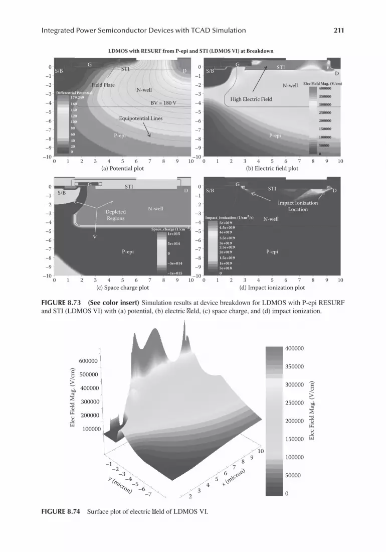
211Integrated Power Semiconductor Devices with TCAD Simulation
0
0–1–2–3–4–5–6–7–8–9
–101 2 3 4 5
(c) Space charge plot
P-epi P-epi
P-epiP-epi
N-well
N-well
N-well
High Electric Field
S/B
S/BS/B
S/BG
GG
GSTISTI
STI STI
D
DD
Field PlateN-well
BV = 180 V
Equipotential Lines
D
DepletedRegions
Impact IonizationLocation
6 7 8 9 10 0
0–1–2–3–4–5–6–7–8–9
–10 0
0
5e+0181e+019
1e+015
–1e+015
1.5e+0192e+0192.5e+0193e+0193.5e+0194e+0194.5e+0195e+019
020406080100120140160179.249
Differential Potential
5e+014
Space_charge (1/cm–3)
–5e+014
Impact_ionization (1/cm3/s)
1 2 3 4 5(d) Impact ionization plot
6 7 8 9 10
0
0–1–2–3–4–5–6–7–8–9
–101 2 3 4 5
(a) Potential plot
LDMOS with RESURF from P-epi and STI (LDMOS VI) at Breakdown
6 7 8 9 10 0
0–1–2–3–4–5
–9–8–7–6
–101 2 3 4 5
(b) Electric field plot6 7
0
50000
100000
150000
200000
250000
300000
350000
400000Elec Field Mag. (V/cm)
8 9 10
FIGURE 8.73 (See color insert) Simulation results at device breakdown for LDMOS with P-epi RESURF and STI (LDMOS VI) with (a) potential, (b) electric field, (c) space charge, and (d) impact ionization.
23
45
67
–7–6
–5–4
–3–2
–1
100000
200000
300000
400000
500000
600000
400000
350000
300000
250000
200000
150000
100000
50000
0
Elec
Fie
ld M
ag. (
V/cm
)
Elec
Fie
ld M
ag. (
V/cm
)
8 910
x (micron)
y (micron)
FIGURE 8.74 Surface plot of electric field of LDMOS VI.

212 Integrated Power Devices and TCAD Simulation
The high breakdown voltage (180 V) seems like overkill for a device designed to handle only 100 V (130 V with safety margin). However, decreasing the on-resistance to achieve better power efficiency often comes at the expense of a lower breakdown voltage, so the large value we achieved gives us a lot of breathing room to make adjustments. To reduce the on-resistance, we need to increase the doping concentration in the N-well; unfortunately, increasing the N-well doping from 5E + 15 cm−3 to 1E + 16 cm−3 while keeping all other parameters the same brings down the break-down voltage to 97 V.
Shown in Figure 8.75 are the simulation results of LDMOS VI with increased N-well doping concentration (1E + 16 cm−3). We note from Figure 8.75a that the equipotential lines are not spread-ing fully inside the N-well. From Figure 8.75b we see that the electric field is crowded at the source side rather than at the drain side. From the space charge plot of Figure 8.75c, a large portion of the N-well region is not depleted, and the impact ionization also seems to take place close to the source side. The reason behind the degradation in breakdown voltage now seems straightforward: the doping concentration in the N-well is too high to be fully depleted by the combined action of the P-body and P-epi regions.
8.3.1.7 LDMOS with Double RESURF (LDMOS VII)By increasing the N-well doping, we are able to reduce the on-resistance, but the breakdown voltage is degraded and drops below our requirements. We need to think of ways to improve the breakdown voltage with the increase in N-well doping.
0 S/BG
Field Plate
STI
N-well
LDMOS with RESURF from P-epi and STI (LDMOS VI) (N-well:1E+16 cm3)
Equipotential Lines
Differential Potential97.05499080706050403020100
P-epi
D
BV = 97 V
–1–2–3–4–5–6–7–8–9
–100 1 2 3 4 5
(a) Potential plot6 7 8 9 10
0 S/BG
High Electric Field
STI
N-well
P-epi
D
400000Elec Field Mag. (V/cm)
350000
300000
250000
200000
150000
100000
50000
1e+015
5e+0204.5e+0204e+0203.5e+0203e+0202.5e+0202e+0201.5e+0201e+0205e+0190
Space_charge (1/cm–3)
5e+014
0
–5e+014
–1e+015
0
–1–2–3–4–5–6–7–8–9
–100 1 2 3 4 5
(b) Electric field plot6 7 8 9 10
0S/B
G
DepletedRegions
STI
N-well UndepletedRegion
P-epi
D–1–2–3–4–5–6–7–8–9
–100 1 2 3 4 5
(c) Space charge plot6 7 8 9 10
0 S/BG
impact_ionization (1/cm3/s
STI
N-well
Impact IonizationLocation
P-epi
D–1–2–3–4–5–6–7–8–9
–100 1 2 3 4 5
(d) Electric field plot6 7 8 9 10
FIGURE 8.75 Simulation results at device breakdown for LDMOS VI with increased N-well doping (1E + 16 cm-3) with (a) potential, (b) electric field, (c) space charge, and (d) impact ionization.

213Integrated Power Semiconductor Devices with TCAD Simulation
The improvements we achieved in LDMOS V were due to the RESURF effect to deplete the N-well from below. Since this is no longer sufficient to fully deplete the region once the N-well doping is increased, a natural development of this idea is to use an additional RESURF region to deplete the N-well from above. This concept is called double RESURF, and its origins can be traced back to 1982 [182]. In this book, we call this additional P-region P-RESURF, and it is left floating (not connected to any contacts or the source/body region). A schematic view of this structure is shown in Figure 8.76a, material plot is shown in Figure 8.76b, while Figures 8.76c and d illustrate the net doping.
Note that in this structure (LDMOS VII) we get rid of the STI region introduced in LDMOS VI for two reasons. First, in real practice the STI process may not be compatible with the double-RESURF P implant step; second, the STI in the drain will increase the total on-resistance. The main differ-ences between this structure and LDMOS V are the doping concentration of the N-well (increased to 1E + 16 cm−3) and the additional P-RESURF region; the channel length is also reduced to 0.7 µm due to the increased doping in the N-well. The simulation parameters are listed in Table 8.12.
The equipotential lines are shown in Figure 8.77a. With double RESURF, the breakdown volt-age increases from 97 V to 157 V with an N-well doping concentration of 1E + 16 cm−3. From the electric field plot of Figure 8.77b, we see multiple high field locations within the device, which is desirable so that the electric field does not concentrate too much in one location. The N-well and P-RESURF regions are fully depleted, as seen from the space charge plot in Figure 8.77c. Impact ionization takes place at the gate edge and at the drain side, as shown in Figure 8.77d.
P+ N+ N+
Source/BodyLMOS with Double RESURF (LDMOS VII)
Drain
Source/Body
Source/BodyGate
Gate
FEM_StructureSiO2
PolySi
Al(xlam=0.55)
P-body
Source/Body Drain
Poly Gate
P-body
P-epi
(a) Schematic view (b) Material plot
P-epi
P-epi
N-well
N-well
N-well
Net_Doping
Log10(Net_Doping)
Log10(Net_Doping)
18161412108642
–1–2–3–4–5–6
y(micron)
8 9 10 15
15.5
16
16.5
17
17.5
18
18.5
19
19
15
10
5
0
–5
–10
–15
–19
Junction LineP-RESURF
0–1–2–3–4–5–6–7–8–9
–100 1 2 3 4 5 6 7 8 9 10
(c) Net doping plot (d) Surface plot of net doping
0–1–2–3–4–5–6–7–8–9
–100 1 2 3 4 5 6 7 8 9 10
P-RESURF
P-RESURF P-RESURF
N-wellSource/
body
P-epi
Drain
DrainDrain
ILD
FIGURE 8.76 LDMOS with double RESURF structure and net doping plot. (a) Schematic view (b) Material plot (c) Net doping plot (d) Surface plot of net doping.

214 Integrated Power Devices and TCAD Simulation
TABLE 8.12Simulation Parameters for LDMOS with Double RESURF (LDMOS VII)
Parameters for Simulation Value
X range 0 to 10 µm
Y range 0 to −20 µm
P-epi 1E + 15 cm−3
P-body max concentration 2E + 17 cm−3
P-body location (x1, x2, dx1, dx2) Gaussian x = (0, 1.5, 0.35, 0.35); y = (−0.6, −0.6, 0.8, 0.8)
N-well max concentration 1E + 16 cm−3
N-well location (x1, x2, dx1, dx2) Gaussian x = (2, 10, 0.25, 0.25); y = (−6, 0, 0.25, 0.25)
P-well double RESURF 1.5E + 16 cm−3
P-well location (x1, x2, dx1, dx2) Gaussian X = (4, 8, 0.25, 0.25); y = (−1, −0.35, 0.25, 0.25)
Oxide thickness 200 Å
Poly gate thickness 0.4 µm
Poly gate length 2 µm
Channel length 0.7 µm (approx.)
Interlayer dielectric thickness 0.7 µm
Source metal shield plate length 6 µm (from source) or 2.5 µm (from gate edge)
(a) Potential plot
0–1–2–3–4–5–6–7–8–9
–100 1 2 3 4 5 6 7 8 9 10
(b) Electric field plot
0–1–2–3–4–5–6–7–8–9
–100 1 2 3 4 5 6 7 8 9 10
(c) Space charge plot
0–1–2–3–4–5–6–7–8–9
–100 1 2 3 4 5 6 7 8 9 10
(d) Imapact ionization plot
0–1–2–3–4–5–6–7–8–9
–100 1 2 3 4 5 6 7 8 9 10
S/B157.444
Differential Potential
Field Plate
N-wellN-well
N-wellN-well
P-epiP-epi
Equipotential Lines
High Electric Field
P-epi P-epi
BV = 157 V
LDMOS with Double RESURF (LDMOS VII) at Breakdown
P-RESURF P-RESURF
P-RESURFP-RESURF
DepletedRegions
Impact Ionization Location
5e+019
1e+015Space_charge (1/cm–3)
5e+014
–5e+014
–1e+015
0
4.5e+0194e+0193.5e+0193e+0192.5e+0192e+0191.5e+0191e+0195e+0180
GGDD S/BS/B
DG G D
S/B
Elec Field Mag. (V/cm)
impact_ionization (1/cm3/s)
400000
350000
300000
250000
200000
150000
100000
50000
0
140
120
100
80
60
40
20
0
FIGURE 8.77 (See color insert) Simulation results after device breakdown for LDMOS VII with increased N-well doping (1E + 16 cm−3) and double RESURF: (a) Potential; (b) Electric field, (c) Space charge; (d) Impact ionization.

215Integrated Power Semiconductor Devices with TCAD Simulation
The key to design the right P-RESURF region is to achieve dose balance in both the P and N-regions: both regions should be completely depleted to achieve optimal results. It is often difficult to make calculations by hand to achieve the right dose balance since the N-well is depleted by a total of three regions: P-body; P-epi; and P-RESURF. TCAD simulation with design of experiments (DoE) is an easy method to achieve the right dose and doping concentrations. In this LDMOS struc-ture, it has been found that for a P-RESURF maximum doping of 1.5E + 16 cm−3, a dose balance can be achieved.
The downside of this double RESURF technology is the addition of the P-RESURF, which will increase the on-resistance and introduce process complexity. In real manufacturing, even a slight process variation may lead to large degradation of breakdown voltage. Also, in practice, the P-RESURF layer is most likely a special purpose layer not shared with other process steps, so an additional mask is required.
A 3D surface plot of electric field is shown in Figure 8.78. We see multiple electric field peaks in the silicon region, which is beneficial for high breakdown voltage.
If we try to get a further reduction of the on-resistance to account for the presence of this addi-tional P-RESURF region, we again encounter the problem of an undepleted N-region. For exam-ple, if we merely increase the N-well doping from 1E + 16 cm−3 to 1.5E + 16 cm−3 while keeping all other parameters the same, the breakdown voltage will drop to 79 V, as illustrated in Figure 8.79.
In Figure 8.79a the equipotential lines are crowded close to the P-body; Figure 8.79b shows the peak electric field locations; from the space charge plot of Figure 8.79c we can easily see that a large portion of the N-well is not depleted. The undepleted area is not able to support the drain voltage, which causes the breakdown voltage to drop. Figure 8.79d shows the location of impact ionization.
As we previously observed, the key to double RESURF is that the N-well is simultaneously being depleted from three sides: the P-body; P-epi; and P-RESURF. With higher N-well doping, the unde-pleted area is close to the drain, which means the depletion regions from P-epi and P-RESURF are not able to meet each other. If the higher N-well doping is a necessity, then the obvious solution that allows these shallower depletion regions to meet is to reduce the N-well depth.
350000
300000
250000
200000
150000
100000
50000
–1–2
–3–4
–5–6
–7 34
56
78
910
0
50000
100000
150000
200000
250000
300000
350000
400000
Elec
Fie
ld M
ag. (
V/cm
)
Elec
Fie
ld M
ag. (
V/cm
)
y (micron)
FIGURE 8.78 Electric field surface plot of LDMOS with double RESURF (LDMOS VII).

216 Integrated Power Devices and TCAD Simulation
If we reduce the N-well depth from about 4.5 µm to 3.35 µm, we can get the breakdown voltage back to 144 V, as illustrated in Figure 8.80. The N-well is almost fully depleted except the top right corner of the drain region: this small pocket area explains why this design is still a few volts lower than the breakdown voltage of our original LDMOS VII design.
Previously when we increased the doping concentration of the N-well from 1E + 16 cm−3 to 1.5E + 16 cm−3, we broke the dose balance between the N-well and P-regions (P-body, P-epi, and P-RESURF), which caused undepleted regions and lowered the breakdown voltage. By reducing the N-well depth, we are also lowering the total dose of the N-well, which creates a more balanced dose in the device. Unfortunately, the on-resistance is dependent on the total dose of the N-well (rather than doping concentration). A simple explanation of this relationship is given as
1 1 1
RLt q N
Lt N t
Lq D
Lqn d d n n
= ρ =µ
=µ
=µ
(8.35)
D N td= (8.36)
where R is the drift region resistance in 2D, ρ is the N-well resistivity, µn is the electron mobility, Nd is the doping concentration in the N-well, L is the N-well length, t is the N-well thickness, and D is the total dose of the N-well. From this equation, we find the resistance in the drain-drift region is inversely proportional to the total dose in the N-well.
(a) Potential plot
0 S/B
S/B S/B
S/B
BV = 79 V
P-RESURF
LDMOS with Double RESURF (LDMOS VII with N-well 1.5E+16 cm–3)
P-RESURF P-RESURF
P-RESURF
Equipotential Lines
High Electric Field
P-epi
Differential Potential Elec field Mag. V/cm)78.6788
1e+015Space_charge (1/cm–3)
impact_ionization (1/cm3/s)5e+0194.5e+019
3.5e+0194e+019
3e+0192.5e+0192e+0191.5e+0191e+0195e+0180–1e+015
5e+014
–5e+014
0
70400000
350000
300000
250000
200000
150000
100000
50000
0
60
50
40
30
20
10
0
N-well
N-wellN-well
N-well
D
D D
DG
G G
–1–2–3–4–5–6–7–8–9
–100 1 2 3 4
P-epi
P-epi P-epi
DepletedRegions
Impact IonizationLocation
UndepletedRegions
5 6 7 8 9 10(b) Electric field plot
0–1–2–3–4–5–6–7–8–9
–100 1 2 3 4 5 6 7 8 9 10
(c) Space charge plot
0–1–2–3–4–5–6–7–8–9
–100 1 2 3 4 5 6 7 8 9 10
(d) Impact ionization plot
0–1–2–3–4–5–6–7–8–9
–100 1 2 3 4 5 6 7 8 9 10
Field Plate
FIGURE 8.79 LDMOS VII with N-well doping concentration increased to 1.5E + 16 cm–3: (a) Potential; (b) Electric field; (c) Space charge; (d) Impact ionization.

217Integrated Power Semiconductor Devices with TCAD Simulation
By reducing the depth of the N-well, we lowered the total dose in the N-well, which leads to a higher on-resistance. This increase can easily offset the benefits we get from increasing the dop-ing concentration in the N-well; thus, once again, improving the breakdown voltage comes at the expense of the on-resistance.
Since the reduction of the N-well depth can backfire, we need to think of other ways to improve the design. Our goal is to keep the increased N-well dose (doping = 1.5E + 16 cm−3) and default thickness (4.5 µm) to maintain a low on-resistance while achieving a breakdown voltage that can meet our specifications (100 V + 30% margin = 130 V). One possibility is to increase the dose of P-RESURF so that it can balance the dose increase in the N-well. Modifying the doping concentra-tions in the P-body and P-epi might also be possible, but this is more difficult in practice since it will inevitably affect other devices on the same chip that share the same process.
To get a rough idea of the P-RESURF dose required to achieve dose balance, we take N-well doping concentration multiplied by N-well depth, so increasing the doping concentration from 1E + 16 cm−3 to 1.5E + 16 cm−3 with the same N-well depth of 4.5 µm results in an dose increase of 2.25E + 12 cm−2. So for a P-RESURF depth of 1 µm, the doping concentration of the P-RESURF should increase by 2.25E + 16 cm−3 from 1.5E + 16 cm−3 to 3.75E + 16 cm−3.
We will use this new P-RESURF dose for the next iteration of our design. As we can see, the simulated breakdown voltage for this structure is only 64 V (Figure 8.81a), which is even worse than for our previous case with a P-RESURF doping of 1.5E + 16 cm−3. The reason behind this degrada-tion is that the depletion region in the N-well from the P-RESURF side fails to reach the depletion region from the P-epi side, as seen in the space charge plot in Figure 8.81c. The high doping of the
(a) Potential plot
0S/BP-RESURF P-RESURF
LDMOS with Double RESURF (LDMOS VII) N-well Depth = 3.35 um
Equipotential Lines
Differential Potential143.647
140
120
100
80
60
40
20
0
N-wellHigh Electric Field N-well
Elec Field Mag. (V/cm)400000
350000
300000
250000
200000
150000
100000
50000
0
BV = 144 V
DG
DG
–1–2–3–4–5–6–7–8–9
–100 1 2 3 4
P-epiP-epi
5 6 7 8 9 10(b) Electric field plot
0–1–2–3–4–5–6–7–8–9
–100 1 2 3 4 5 6 7 8 9 10
Depth = 3.35 um
(c) Space charge plot
0S/BP-RESURF P-RESURF
A smallundepleted pocket
Impact IonizationLocation
N-wellimpact_ionization (1/cm3/s)
5e+0194.5e+0194e+0193.5e+0193e+0192.5e+0192e+0191.5e+0191e+0195e+0180
Space_charge (1/cm–3)1e+015
–1e+015
5e+014
–5e+014
0
DG
DG
S/B–1–2–3–4–5–6–7–8–9
–100 1 2 3 4
P-epi P-epi
5 6 7 8 9 10(d) Impact ionization plot
0–1–2–3–4–5–6–7–8–9
–100 1 2 3 4 5 6 7 8 9 10
DepletedRegions
FIGURE 8.80 LDMOS VII with N-well doping concentration increased to 1.5E + 16 cm–3 and N-well depth reduced to 3.35 µm: (a) Potential; (b) Electric field; (c) Space charge; (d) Impact ionization.

218 Integrated Power Devices and TCAD Simulation
P-RESURF also prevents this floating island from being fully depleted. Due to high doping concen-trations in both the P-RESURF and N-well, a high electric field is present at this junction (Figure 8.81b) which causes impact ionization as shown in Figure 8.81d.
8.3.1.8 LDMOS Multiple RESURF (LDMOS VIII)From our previous design (LDMOS VII), we have learned that the N-well in a double RESURF structure cannot be fully depleted if we want a high N-well doping (e.g., 1.5E + 16 cm−3), unless we reduce the N-well depth. But this is not useful because the total dose in the N-well is also reduced and the on-resistance depends on the total N-well dose rather than the N-well doping concentration.
An ingenious idea to work around this problem was proposed by engineers (circa 2000): the P-RESURF does not necessarily have to reside on top of the N-well [183], [184], [185]. This floating region can instead stay floating in the middle of the N-well as a RESURF island. The idea is that the island of P-RESURF now separates the N-well into upper and lower portions. This, in effect, reduces the required depletion thickness so that it is easier to deplete the entire N-well.
We call this implementation of RESURF multiple RESURF, as it has multiple RESURF junc-tions in the N-well and is more effective in mutual depletions than double RESURF or single RESURF. A schematic of this structure is given in Figure 8.82a.
Figure 8.82b shows the material plot, while Figures 8.82c and 8.82d plot the net doping in the device. The P-RESURF is now floating somewhere in the middle of the N-well but not at the exact center; we will discuss this a little bit later. The doping concentration of the N-well is 1.5E + 16 cm−3, while the maximum doping in the P-RESURF is chosen as 4.5E + 16 cm−3. The location and doping
(a) Potential plot
0 S/BP-RESURF (3.75E+16 cm–3) P-RESURF (3.75E+16 cm–3)
LDMOS with Double-RESURF (LDMOS VII P-RESURF 3.75+16 cm–3)
Equipotential Lines
Differential Potential64.4154
60
50
40
30
20
10
0
N-wellHigh Electric Field
N-well
BV = 64 V
DG
DG
–1–2–3–4–5–6–7–8–9
–100 1 2 3 4
P-epiP-epi
5 6 7 8 9 10(b) Electric field plot
0–1–2–3–4–5–6–7–8–9
–100 1 2 3 4 5 6 7 8 9 10
(c) Space charge plot
0S/B
1e+015space_charge (1/cm–3)
5e+014
0
–5e+014
–1e+015
DepletedRegions Impact Ionization Location
P RESURF
impact_ionization (1/cm3/s)1e+020
8e+019
6e+019
4e+019
2e+019
0
Undepleted
DG
S/B DG
–1–2–3–4–5–6–7–8–9
–100 1 2 3 4
P-epi P-epi
5 6 7 8 9 10(d) Impact ionization plot
0–1–2–3–4–5–6–7–8–9
–100 1 2 3 4 5 6 7 8 9 10
Elec Field Mag. (V/cm)400000
350000
300000
250000
200000
150000
100000
50000
0
FIGURE 8.81 LDMOS VII with N-well doping concentration increased to 1.5E + 16 cm–3 and P-RESURF changed to 3.75E + 16 cm−3: (a) Potential; (b) Electric field; (c) Space charge; (d) Impact ionization.
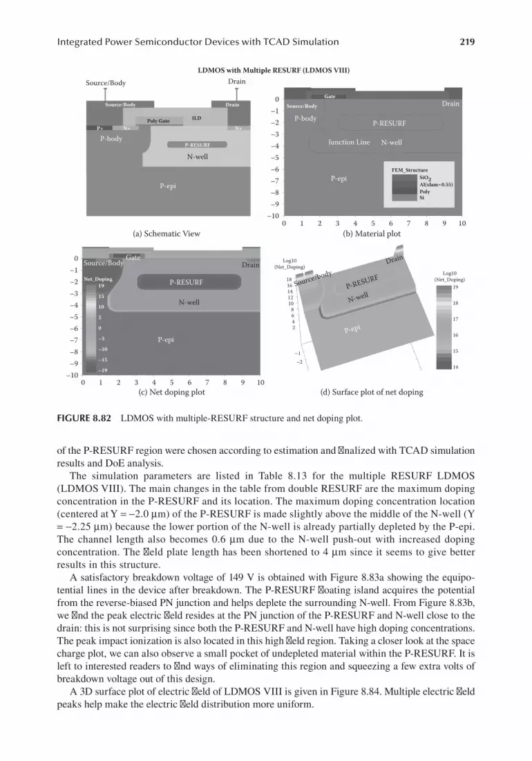
219Integrated Power Semiconductor Devices with TCAD Simulation
of the P-RESURF region were chosen according to estimation and finalized with TCAD simulation results and DoE analysis.
The simulation parameters are listed in Table 8.13 for the multiple RESURF LDMOS (LDMOS VIII). The main changes in the table from double RESURF are the maximum doping concentration in the P-RESURF and its location. The maximum doping concentration location (centered at Y = −2.0 µm) of the P-RESURF is made slightly above the middle of the N-well (Y = −2.25 µm) because the lower portion of the N-well is already partially depleted by the P-epi. The channel length also becomes 0.6 µm due to the N-well push-out with increased doping concentration. The field plate length has been shortened to 4 µm since it seems to give better results in this structure.
A satisfactory breakdown voltage of 149 V is obtained with Figure 8.83a showing the equipo-tential lines in the device after breakdown. The P-RESURF floating island acquires the potential from the reverse-biased PN junction and helps deplete the surrounding N-well. From Figure 8.83b, we find the peak electric field resides at the PN junction of the P-RESURF and N-well close to the drain: this is not surprising since both the P-RESURF and N-well have high doping concentrations. The peak impact ionization is also located in this high field region. Taking a closer look at the space charge plot, we can also observe a small pocket of undepleted material within the P-RESURF. It is left to interested readers to find ways of eliminating this region and squeezing a few extra volts of breakdown voltage out of this design.
A 3D surface plot of electric field of LDMOS VIII is given in Figure 8.84. Multiple electric field peaks help make the electric field distribution more uniform.
P+ N+ N+
Source/BodyLDMOS with Multiple RESURF (LDMOS VIII)
Drain
Source/Body
Source/BodyGate
Gate
FEM_StructureSiO2
PolySi
Al(xlam=0.55)
P-body
Source/Body Drain
Poly Gate
P-body
P-epi
(a) Schematic View (b) Material plot
P-epi
P-epi
N-well
N-well
N-well
Net_Doping
Log10(Net_Doping)
Log10(Net_Doping)18
16141210
8642
–1–2
14
15
16
17
18
1919
15
10
5
0
–5
–10
–15
–19
Junction LineP-RESURF
0–1–2–3–4–5–6–7–8–9
–100 1 2 3 4 5 6 7 8 9 10
(c) Net doping plot (d) Surface plot of net doping
0–1–2–3–4–5–6–7–8–9
–100 1 2 3 4 5 6 7 8 9 10
P-RESURF
P-RESURF P-RESURF
N-wellSource/body
P-epi
Drain
Drain Drain
ILD
FIGURE 8.82 LDMOS with multiple-RESURF structure and net doping plot.
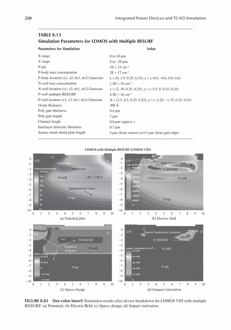
220 Integrated Power Devices and TCAD Simulation
TABLE 8.13Simulation Parameters for LDMOS with Multiple RESURF
Parameters for Simulation Value
X range 0 to 10 µm
Y range 0 to −20 µm
P-epi 1E + 15 cm−3
P-body max concentration 2E + 17 cm−3
P-body location (x1, x2, dx1, dx2) Gaussian x = (0, 1.5, 0.35, 0.35); y = (−0.6, −0.6, 0.8, 0.8)
N-well max concentration 1.5E + 16 cm−3
N-well location (x1, x2, dx1, dx2) Gaussian x = (2, 10, 0.25, 0.25); y = (−5.5, 0, 0.25, 0.25)
P-well multiple-RESURF 4.5E + 16 cm−3
P-well location (x1, x2, dx1, dx2) Gaussian X = (3.5, 8.5, 0.25, 0.25); y = (−2.25, −1.75, 0.25, 0.25)
Oxide thickness 200 Å
Poly gate thickness 0.4 µm
Poly gate length 2 µm
Channel length 0.6 µm (approx.)
Interlayer dielectric thickness 0.7 µm
Source metal shield plate length 4 µm (from source) or 0.5 µm (from gate edge)
(a) Potential plot
0
P-RESURF
LDMOS with Multiple RESURF (LDMOS VIII)
Equipotential Lines
Differential Potential149.163
140
120
100
80
60
40
20
0
N-well BV = 149 V
DG
S/B–1–2–3–4–5–6–7–8–9
–100 1 2 3 4
P-epi
5 6 7 8 9 10
Field Plate
(b) Electric field
0–1–2–3–4–5–6–7–8–9
–100 1 2 3 4 5 6 7 8 9 10
N-well
High Electric Field
P-epi
P-RESURF
S/BG
Elec Field Mag. (V/cm)400000
350000
300000
250000
200000
150000
100000
50000
0
(d) Imapact ionization
0–1–2–3–4–5–6–7–8–9
–100 1 2 3 4 5 6 7 8 9 10
(c) Space charge
0–1–2–3–4–5–6–7–8–9
–100 1 2 3 4 5 6 7 8 9 10
N-well
P-epi
P-RESURF
Impact Ionization Location
1e+021
8e+020
6e+020
4e+020
2e+020
0
GDS/B
impact_ionization (1/cm3/sN-well
P-epi
P-RESURF
DepletedRegions
1e+015Space_charge (1/cm–3)
5e+014
–5e+014
–1e+015
0
GDS/B
FIGURE 8.83 (See color insert) Simulation results after device breakdown for LDMOS VIII with multiple RESURF: (a) Potential; (b) Electric field; (c) Space charge; (d) Impact ionization.

221Integrated Power Semiconductor Devices with TCAD Simulation
8.3.1.9 Comparison of 3D Surface Plot of Electric FieldA grand comparison is made among the eight LDMOS structures, as shown in Figure 8.85. LDMOS structures with N-epi (LDMOS I to IV) have considerably inferior breakdown voltages than LDMOS structures with P-epi RESURF (LDMOS V to VIII). LDMOS structures with N-epi have a triangle-shaped electric field compared with the more uniform and multiple peaked electric field distribution exhibited by LDMOS with P-epi RESURF. A well-designed LDMOS with double RESURF or mul-tiple RESURF can handle high breakdown voltage with low on-resistance, thanks to the increased N-well doping that is made possible by the RESURF effect.
LDMOS designs have evolved over the past decades: many structures including multiple RESURF have been developed, and several are covered by patents. New ideas and novel structures continue to be published, and designers are wise to keep up to date with the latest concepts as this book cannot cover the entirety of this topic. Useful academic conferences and journals for this topic include the IEEE International Symposiums on Power Semiconductor Devices and ICs and the International Electron Devices Meeting.
8.3.2 pArAsitic npn BJts in ldmos
Unlike a digital or analog MOSFET, a power LDMOS has the source/body shorted to form a simple PN junction diode between drain and source/body. One of the reasons for doing this is because there is a parasitic N (drain-drift) − P (P-body) − N (N+ source) BJT, as shown in Figure 8.86. A floating body region (body P+ contact removed) might cause a BVCEO type of breakdown if a large voltage drop within the P-body region were to trigger forward biasing of the P-body/N+ source junction (base-emitter junction of the parasitic NPN).
As an example, the LDMOS with STI (LDMOS III) is used with body contact removed (contact covers only the N+ source). Shown in Figure 8.87b, the floating body leads to a BVCEO type of break-down and greatly reduces the breakdown voltage from 87 to 35 V, and a large leakage current flows from the drain (collector in the parasitic NPN BJT) through the P-body (base of the parasitic NPN BJT) to the source (emitter of the parasitic NPN BJT). Figure 8.87a is a comparison of the same
40000035000030000025000020000015000010000050000
–1–2
–3–4
–5–6 4
56
78
910
0
50000
100000
150000
200000
250000
300000
350000
400000
Elec
Fie
ld M
ag. (
V/cm
)
Elec
Fie
ld M
ag. (
V/cm
)
FIGURE 8.84 Electric field surface plot of LDMOS with multiple RESURF (LDMOS VIII).

222 Integrated Power Devices and TCAD Simulation
3500
00
Elec
Fie
ld M
ag.
(V/c
m)
Elec
Fie
ld M
ag.
(V/c
m)
Elec
Fie
ld M
ag.
(V/c
m)
Elec
Fie
ld M
ag.
(V/c
m)
Elec
Fie
ld M
ag.
(V/c
m)
Elec
Fie
ld M
ag.
(V/c
m)
3000
0025
0000
2000
0015
0000
1000
0050
000
3500
00
4000
00
3000
00
2500
00
2000
00
1500
00
1000
00
5000
0
0
Elec
Fie
ld M
ag.
(V/c
m)
Elec
Fie
ld M
ag.
(V/c
m)
3500
0040
0000
8000
0070
0000
6000
0050
0000
4000
0030
0000
2000
0010
0000
6000
0050
0000
4000
0030
0000
2000
0010
0000
3000
0025
0000
2000
0015
0000
1000
0050
000
0
3500
00
4000
00
3000
00
2500
00
2000
00
1500
00
1000
00
5000
0
0
5000
00
6000
00
7000
00
4000
00
3000
00
2000
00
1000
00
0
–1–2 –3
–4 –5–6 –7
y(micr
on)
y(micr
on)
y(micr
on)
y(micr
on)
(a) N
-epi
(LD
MO
S I),
BV
= 46
V an
dN
= 5
E15
cm–3
(b) N
-epi
and
field
pla
te (L
DM
OS
II),
BV =
89
V an
d N
= 5
E15
cm–3
LDM
OS
I to
IV w
ith N
-epi
LDM
OS
V to
VII
I with
P-e
pi R
ESU
RF
(c) N
-epi
and
STI (
LDM
OS
III),
BV =
87
V an
d N
= 5
E15
cm–3
(d) N
-epi
, fiel
d pl
ate a
nd S
TI (L
DM
OS
IV),
BV =
88
V an
d N
= 5
E15
cm–3
x(micr
on)
x(micr
on)
x(micr
on)
x(micr
on)
N-epi
Drain
P-bo
dy
S/B
–8–9
12
34
56
78
910
4000
0035
0000
Elec
Fie
ld M
ag.
(V/c
m)
Elec
Fie
ld M
ag.
(V/c
m)
3000
0025
0000
2000
0015
0000
1000
0050
000
3500
00
4000
00
3000
00
2500
00
2000
00
1500
00
1000
00
5000
0
0
–1–2
–3–4
–5–6
–7y(m
icron
)
y(micr
on)
y(micr
on)
y(micr
on)
(e) P
-epi
RES
URF
(LD
MO
S V
),BV
= 1
48 V
and
N =
5E1
5 cm
–3(f
) P-e
pi R
ESU
RF an
d ST
I (LD
MO
S VI
),BV
= 1
80 V
and
N =
5E1
5 cm
–3(g
) P-e
pi d
oubl
e RES
URF
(LD
MO
S VI
I),BV
= 1
57 V
and
N =
1E1
6 cm
–3(h
) P-e
pi m
ultip
le R
ESU
RF (L
DM
OS
VIII)
,BV
= 1
49 V
and
N =
1.5
E16
cm–3
x(m
icron
)
x(micr
on)
–8–9
–10
12
34
56
78
910
6000
0060
0000
Elec
Fie
ld M
ag.
(V/c
m)
Elec
Fie
ld M
ag.
(V/c
m)
Elec
Fie
ld M
ag.
(V/c
m)
Elec
Fie
ld M
ag.
(V/c
m)
Elec
Fie
ld M
ag.
(V/c
m)
4000
0030
0000
2000
0010
0000
3500
00
4000
00
3000
00
2500
00
2000
00
1500
00
1000
00
5000
0
3500
0030
0000
2500
0020
0000
1500
0010
0000
5000
0
3500
0040
0000
3000
0025
0000
2000
0015
0000
1000
0050
000
0
3500
00
4000
00
3000
00
2500
00
2000
00
1500
00
1000
00
5000
0
0
Elec
Fie
ld M
ag.
(V/c
m) 35
0000
4000
00
3000
00
2500
00
2000
00
1500
00
1000
00
5000
0
0
–1–2
–3–4
–5–6
–7
–1 –2 –3 –4 –5 –6 –7
–1 –2–3 –4
–5–6
23
45
67
8910
34
56
78
910
45
67
8910
3500
0040
0000
3000
0025
0000
2000
0015
0000
1000
0050
000 –1
–2 –3–4 –5
–6–7
N-epi
Drain
P-bo
dy
S/B
N-epi
Drain
P-body
S/B
N-epi
Drain
P-bod
y
S/B
–8–9
12
34
56
78
910
–1 –2–3
–4–5
–6–7
–8–9
12
34
56
78
910
12
34
56
78
910
–1–2
–3–4
–5–6
–7–8
–9
FIG
UR
E 8.
85
(See
col
or in
sert
) C
ompa
riso
n of
ele
ctri
c fie
ld s
urfa
ce p
lots
of
all L
DM
OS
stru
ctur
es d
iscu
ssed
.

223Integrated Power Semiconductor Devices with TCAD Simulation
LDMOS (LDMOS III) with the body contact connected to the source (standard). The drain voltage is biased to 35 V, and no noticeable leakage current exists.
In fact, even with the body connected to the source, the parasitic BJT may still be turned on when carrying a large leakage current flow (BVCES type of breakdown), since the voltage drop in the body region may be higher than the built-in potential of the body (base) to source (emitter) PN junction. Forward biasing of the base-emitter of the parasitic NPN BJT may cause permanent damage to the device with a second breakdown (thermal runaway): this phenomenon will be dis-cussed later.
8.3.3 ldmos on-stAte resistAnce
Most of the time power LDMOS are working in either on- or off-states. During the on-state, the gate is biased so that the device is fully turned on: current flows from drain terminal, through the drain-drift region, and into the channel region before finally reaching the source/body terminal.
Rbody
P-body
N+ N+P+
Drain-Drift Region
N N-epi
Gate
Gate
Source/Body Drain
FIGURE 8.86 Parasitic NPN BJT in LDMOS.
(a) LDMOS III leakage current plot at 35 V (b) LDMOS III leakage current plot at 35 V (withonly source contact and body floating)
0
Leakage current withbody contact
Standard Source/bodycontact
LDMOS III simulated @ 35 VBreakdown voltage is 87 V
Leakage Current Comparison with/without Body Contact
Total Curr. Mag (A/cm2)0.001
0.0008
0.0006
0.0004
0.0002
0
DG
S/B–1–2–3–4–5–6–7–8–9
–100 1 2 3 4 5 6 7 8 9 10
0
Leakage currentwithout body contact
P-body contactremoved
LDMOS III with bodycontact removed after
breakdown @ 35 V
Total Curr. Mag (A/cm2)500450400350300250
150200
100500
DG
S/B–1–2–3–4–5–6–7–8–9
–100 1 2 3 4 5 6 7 8 9 10
FIGURE 8.87 If body is left floating, BVCEO type of breakdown occurs, resulting in large current flowing through the parasitic BJT.

224 Integrated Power Devices and TCAD Simulation
The on-resistance of the LDMOS can be analyzed with several contributing resistances connected in series. We will use the simple LDMOS with N-epi (LDMOS I) as an example. Figure 8.88 shows the resistance components of an LDMOS. The total on-resistance is thus the sum of these components:
R R R R R Ron cs ch acc drift cd= + + + + (8.37)
where Rcs and Rcd are the contact resistances of source and drain, which are generally quite small and will be omitted in this book. Rch is the channel resistance, which can be calculated using the standard equation that is also used for digital and analog MOSFETs:
2 ( )
RL
C V Vch
i ox G th
=µ − (8.38)
where µi is the inversion layer mobility for electrons (n-LDMOS) and holes (p-LDMOS), VG is the gate voltage, Vth is the threshold voltage, and L is the channel length. Cox is the gate capacitance and is calculated in 2D by
Ct
oxox= ε
(8.39)
where εox is the dielectric constant of oxide, t is the gate oxide thickness.The accumulation resistance Racc is unique for DMOS (LDMOS and VDMOS). It represents the
resistance in the silicon area that is overlapped by gate and drain. The word accumulation means that the overlapped area is in accumulation mode when the gate is turned on. For an n-LDMOS device during on-state, this happens when a sufficiently high positive voltage is applied to the gate: the positive voltage attracts electrons to the overlapped area and lowers the resistance for drain cur-rent flow. The accumulation resistance can be calculated by [186].
4 ( )
RL
C V Vacc
acc
a ox G th
=µ −
(8.40)
Rcs Rch Racc Rdrift
LdriftLaccLch
GateSource/Body
Rcd
Drain
FIGURE 8.88 LDMOS on-resistance.

225Integrated Power Semiconductor Devices with TCAD Simulation
where Lacc is the accumulation region length, which is from the body/drain PN junction to the gate edge in the drain, and µa is the electron or hole mobility in the accumulation layer. Because of the local field, electrons generally have a higher mobility in the accumulation layer than in the inversion layer.
The drift region resistance Rdrift is calculated using
RL
d
L
q N d
L
q Ddrift
drift
eff
drift
n d eff
drift
n eff
= ρ =µ
=µ
(8.41)
D N deff d eff= (8.42)
where Ldrift is the drift length, deff is the effective N-well thickness due to unequal distribution of cur-rent flow, Nd is the doping concentration in the drain, µn is the electron mobility in the drift region, and Deff is the effective total dose in the drain, with n-LDMOS assumed.
8.3.3.1 Specific On-ResistanceTo compare resistance of LDMOS with different technology or vendors, it is convenient to use specific on-resistance, Ron, sp or Rsp, instead of pure resistance; the difference is that specific on-resistance takes device pitch size into consideration. The pitch size is calculated from body contact edge to drain edge. Note that in real devices body and drain are shared with neighboring devices: in that case, the middle point of the body and drain contacts should be used. As an example, most simulated LDMOS in this book use a pitch size of 10 µm. The unit used in this book for specific resistance is m cmΩ 2⋅ .
8.3.3.2 On-Resistance ContributionTo find out how much contribution the channel region and drift region have for the total resistance, we can simulate a truncated area of the LDMOS. For example, since accumulation resistance is rela-tively small compared with drift resistance, we can combine them into a simple channel resistance. Figure 8.89 is the test structure for on-resistance simulation from channel and accumulation regions only: a test contact is added under the edge of the gate in the drain-drift region to inject carriers in the simulation. The drain region is very short, so it is ignored and small amounts of N+ doping are
0
–1
–2
–3
–4
–5
–6
–7
–8
–9
–100 025
–18.9998
–15
–10
N-epi–5
0
5
10
15
19
(donor_conc/acceptor_conc/)Signed_Log10
Source/Body
P-body
Test
Con
tact
Gate
0.5 0.75 1 1.25 1.5 1.75 2 2.25 2.5 2.75
FIGURE 8.89 Test structure for LDMOS on-resistance.

226 Integrated Power Devices and TCAD Simulation
added to create an Ohmic boundary for our test contact. The total length of this test structure is 2.75 µm, including the drain region, which is only 0.25 µm.
For the simple LDMOS with an N-epi doping concentration of 5E + 15 cm−3 (LDMOS I), a pitch size of 10 µm, and a gate voltage bias of 5 V, the simulation result shows the channel resistance is only 0.2 ⋅mΩ cm2 (pitch size of 10 µm is used in calculation of specific on-resistance for comparison), while the total resistance for the LDMOS I with standard drain-drift length is 2.78 ⋅mΩ cm2. Therefore, we can conclude that the majority of the on-resistance comes from the drain-drift region. However, for low breakdown voltage LDMOS (< 25 V), the drain length is much shorter and the doping concentration is much heavier; therefore, the on-resistance from the channel can be greater than that from the drain.
8.3.3.3 Comparison of Breakdown Voltage and On-ResistanceA comparison is made among the LDMOS discussed before, as illustrated in Table 8.14. The simple N-epi LDMOS (LDMOS I) has the lowest breakdown voltage of 46 V and a relatively low specific on-resistance of 2.78 ⋅mΩ cm2. With the addition of field plate (LDMOS II), the breakdown volt-age increases significantly to 89 V while on-resistance stays the same. With added STI (LDMOS III), the breakdown is similar to LDMOS with a field plate (LDMOS II), but the on-resistance of LDMOS III increases by 40% over LDMOS I: this is caused by the presence of oxide in the drain-drift region, which reduces the accumulation length and makes part of the silicon surface unavail-able for current flow. When the field plate and STI are combined (LDMOS IV), the breakdown voltage stays the same, while the on-resistance is similar to that of LDMOS III. In fact, further optimizing the field plate or STI will only show small changes of breakdown voltage.
With P-epi RESURF (LDMOS V), breakdown voltage increases significantly for the same N-well doping concentration (5E + 15 cm−3) and specific on-resistance is similar to LDMOS I at 2.79 ⋅mΩ cm2. The added STI combined with increased N-well doping (1E + 16 m−3) in LDMOS VI causes the breakdown voltage to drop back down to the level of LDMOS IV while the on-resistance is reduced to 2.09 ⋅mΩ cm2. To further increase breakdown voltage to satisfy the design spec, double RESURF (LDMOS VII) is used: a much higher breakdown voltage (157 V) is obtained with N-well doping concentration of 1E + 16 cm−3, but the on-resistance rises to 3.07 ⋅mΩ cm2 due to the reduced total dose in the N-well and the presence of the P-RESURF layer. (P-RESURF has a depth of about 1 µm, while the depth of STI is only 0.35 µm.) Finally, the multiple RESURF method is applied (LDMOS VIII) to create a floating P-RESURF island to help deplete the entire N-well region. Even with a higher doping concentration of 1.5E + 16 cm−3, the breakdown voltage is increased to 149 V and the on-resistance drops to 1.66 ⋅mΩ cm2, the lowest value among all our designs.
Figure of merits (FOM), which is defined by BV2/Ron, sp, is included in Table 8.14. This FOM allows us to compare LDMOS structures in a more straightforward way. We see LDMOS I has the
TABLE 8.14Comparison of Breakdown Voltage and Specific On-Resistance
LDMOS Structures (Types)N-well doping
(cm–3)Breakdown
(V)Ron,sp
(mΩ cm2)FOM
(BV2/Ron,sp)
N-epi (LDMOS I) 5E + 15 46 2.78 762
N-epi + field plate (LDMOS II) 5E + 15 89 2.64 3000
N-epi + STI (LDMOS III) 5E + 15 87 3.94 1920
N-epi + field plate + STI (LDMOS IV) 5E + 15 88 3.91 1980
P-epi + field plate + single RESURF (LDMOS V) 5E + 15 146 2.79 7630
P-epi + field plate + STI + single RESURF (LDMOS VI) 1E + 16 97 2.09 4500
P-epi + field plate + double RESURF (LDMOS VII) 1E + 16 158 3.07 8140
P-epi + field plate + multiple RESURF (LDMOS VIII) 1.5E + 16 149 1.66 13400

227Integrated Power Semiconductor Devices with TCAD Simulation
lowest FOM (762) while LDMOS VIII has the highest (13400). For LDMOS with N-epi, LDMOS II is a better choice with higher FOM than that of LDMOS III or IV.
8.3.4 ldmos tHresHold voltAge
For LDMOS, the threshold voltage design is similar to analog or digital MOSFET. However, unlike analog or digital MOSFET, an LDMOS P-body region is created by diffusion of an implant under-neath the gate, which means that a doping concentration gradient exists in the channel region. Since higher P-body doping concentration yields higher threshold voltage, the threshold voltage is determined by the peak P-body doping concentration in the channel, near the source side.
For the gate oxide design, a thicker oxide yields a higher threshold voltage. For power devices with high gate voltage supplies, a thicker oxide is necessary to reduce gate leakage current and improve long-term oxide reliability (e.g., TDDB). A properly designed threshold voltage is always important for IC designers (neither too low nor too high). Oftentimes, multiple levels of threshold voltages are necessary for digital, analog, and power MOSFETs, and multiple oxide thicknesses in the same process flow is desired.
The LDMOS I with N-epi is simulated, and the threshold voltage is found to be close to 0.83 V. The threshold voltage is extracted using the peak transconductance (Gm) method [39]:
1. Plot ID-VG at low VD value (e.g. VD = 0.1 V). 2. Plot the slope of ID-VG to get the transconductance curve. 3. Select VG at maximum transconductance and use the VG value to find the (VG,Gm.max, ID,Gm.max)
point on the ID-VG curve. 4. Draw a tangent line through the (VG,Gm.max, ID,Gm.max) point and let it intercept the voltage
axis of the ID-VG plot. This intercept is defined as Vth.
The threshold voltage is plotted in Figure 8.90, with the transconductance Gm-VG curve and tan-gent line to extract threshold voltage. For analytical calculations, threshold voltage is calculated using
2VQC
QC
T msi
i
d
if= φ − − + φ (8.43)
2.82.62.42.2
21.81.61.41.2
10.80.60.40.2
Dra
in C
urre
nt (A
/m)
Tran
scon
duct
ance
(Gm
) (A
/Vm
)
0
9.745679
8
7
6
5
4
3
2
1
6.46266e–0080 0.1 0.2 0.3 0.4 0.5 0.6 0.7
Gate Voltage (V)
(VG, Gm.max ID,Gm.max)
Gm.max
0.8 0.9 1 1.1 1.2 1.3 1.4
Vth = 0.83 V
Gm
Id
FIGURE 8.90 Threshold voltage plot of simple LDMOS (LDMOS I).

228 Integrated Power Devices and TCAD Simulation
where Qi is the interface charge, Qd is the depletion charge, and ϕms is the work function potential difference between the gate and semiconductor:
ms m sφ = φ −φ (8.44)
ϕf is the Fermi level:
kTq
Nn
fA
i
lnφ =
(8.45)
In the power device and power IC industry, sometimes it is more convenient to define threshold voltage using a certain drain current value.
Plots of Id-Vg curves at different temperatures are illustrated in Figure 8.91. It has been observed that beyond a certain gate voltage range the drain current decreases with increasing temperature due to reduced mobility at elevated temperatures. This negative temperature coefficient is desirable for power devices to reduce the risk of thermal runaway. Unfortunately, below certain gate voltage range, the current increases with higher temperature: this small region of positive temperature coef-ficient is caused by lower threshold voltage at elevated temperatures. This means there is a small region where positive feedback loops similar to those of BJT are possible, and it is recommended to avoid operating devices in this region.
8.3.5 ldmos witH rAdiAtion HArdening design
For applications involving outer space, high-altitude flights, or operations around nuclear reactors, power devices should be designed to withstand ionizing radiation such as high-energy protons, alpha particles, x-rays, and gamma rays. Most semiconductor devices are susceptible to radiation damage,
2.50
300 K350 K400 K450 K
2.25
2.00
1.75
1.50
1.25
1.00
0.75Dra
in C
urre
nt (A
/m)
0.50
0.25
0.00
Gate Voltage (V)
Id-Vg Curves at Different Temperatures (LDMOS I)
0.2 0.3 0.4 0.5 0.6 0.7 0.8 0.9 1.0 1.1 1.2 1.3
Negative TemperatureCoefficient Region
Positive TemperatureCoefficient Region
FIGURE 8.91 Id-Vd curves with different temperatures (LDMOS I).

229Integrated Power Semiconductor Devices with TCAD Simulation
and radiation hardening design refers to designs that reduce the susceptibility of semiconductor devices to radiation damage.
Radiation damage comes in many forms and the exact details of the defects created by a radia-tion source depend on the particle’s mass and energy; experimental measurements through deliber-ate irradiation or Monte Carlo simulation with tools such as GEANT [187] are needed to get this kind of information. However, one commonly observed consequence of ionizing radiation is the creation of positive fixed sheet charges and acceptor-like deep level traps at the oxide/silicon inter-face. The effect of deep-level acceptors near the silicon channel is similar to an increase of channel P-doping, which would shift the threshold voltage of an n-LDMOS upward. On the other hand, add-ing a positive fixed charge to the channel interface has an effect similar to n-doping, which shifts the threshold voltage downward [39].
Radiation hardening simulation is carried out using the basic LDMOS (LDMOS I), as seen in Figure 8.92. For the purposes of simulation, we assume additional positive fixed charges with a sur-face density of 8E + 11 cm−2 and deep acceptor traps of 2E + 11 cm−2 located at 0.4, 0.6, and 0.8 eV, respectively, below the conduction band. The net effect of the radiation is a downward shift of the threshold voltage from 0.83 to 0.55 V.
8.3.6 ldmos i-v FAmily oF curves
The I-V family of curves is a set of drain voltage-current curves at various applied gate voltages: these curves are especially important for analog amplification applications. We will use LDMOS with N-epi (LDMOS I; see net doping plot in Figure 8.93a) as a test structure. The I-V curves under various gate voltages (1.5 V, 2.0 V, 2.5 V, 3.0 V, 3.5 V, 4.0 V, and 4.5 V) are given in Figure 8.93b.
From Figure 8.93b, we notice the I-V curves for gate voltages above 3.5 V exhibit a significant drain current saturation effect. This current saturation (or the so-called quasi-saturation) is differ-ent from the channel current saturation, which is caused by the pinch-off of the channel. Quasi-saturation is instead caused by carrier velocity saturation in the drain-drift region.
A modified LDMOS (Figure 8.93c) is used for comparison purposes. It is the same LDMOS except that the N+ drain is moved to the gate side to reduce the drain-drift region length. With a very short drain-drift region, we see no quasi-saturation effect in the I-V curves, as shown in Figure 8.93d.
3.5
3
2.5
2
1.5
1
0.5
Dra
in C
urre
nt (A
/m)
00 0.25 0.5 0.75 1
Gate Voltage (V)1.25 1.5 1.75 2
Normal LDMOS Id – Vg
Radiation Hardening vs. Standard (Id – Vg curve)
With radiation simulation
FIGURE 8.92 Radiation hardening simulation compared with normal LDMOS Id-Vg curve.

230 Integrated Power Devices and TCAD Simulation
For LDMOS to sustain a high breakdown voltage, the drain-drift region is usually lightly doped. The drain current density JD can be expressed as
J qn E qnvD n n= µ = (8.46)
v En n=µ (8.47)
where n is the electron carrier density, µn is the mobility of electron, = × −q C1.602 10 , 19 is the electron charge, vn is the electron velocity, and E is the electric field in the drift region.
For a given current density JD and field value E, if the carrier density/doping concentration is sufficiently high (i.e., > 1E + 18 cm−3), then vn does not set a constraint and the desired current value can be attained. However, if we have a lightly doped drain-drift region, then the maximum value of vn, the saturation velocity, fixes a limit beyond that the current cannot increase any more: this causes the quasi-saturation of JD.
8.3.7 ldmos selF-HeAting
When a large current passes through the transistor, the lattice temperature goes up with self-heating. This self-heating can be localized. Unlike bipolar devices, where localized self-heating causes a
N-epi
Net_Doping19
15
10
5
0
–5
–10
–15
–18.9998
DrainGate
S/B
N-epi
Net_Doping19
15
10
5
0
–5
–10
–15
–18.9998
GateSource/Body
Vg = 3.5 V
LDMOS with N-epi (LDMOS I)
Modified LDMOS I with Short Drain-Drift Region
(a) Net doping plot of LDMOS I
0
Dra
in C
urre
nt (A
/m)
–1–2–3–4–5–6–7–8–9
–10
225
200
175
150
125
100
75
50
25
0 1 2 3 4 5 6 7 8 9 10 Drain Voltage (V)(b) I-V curves of LDMOS I
1 2 3 4 5 6 7 8 9 10 11 12 13 14 15
(c) LDMOS with short drain-drift region (modifiedLDMOS I)
0Drain
Dra
in C
urre
nt (A
/m)
–1–2–3–4–5–6–7–8–9
–10
500550
450400350300250200150100
50
0 0.50.25 0.75 1.251 1.5 1.75 2 2.25 2.5 2.75 3 3.25 3.5 3.75Drain Voltage (V)
(d) I-V curves of modified LDMOS I with shortdrain-drift region
1 2 3 4 5 6 7 8 9
Vg = 1.5 VVg = 2.0 VVg = 2.5 V
Vg = 3.0 V
Vg = 3.5 V
Vg = 4.0 V
Vg = 4.5 V
Vg = 4.0 V
10 11 12 13 14 15
Vg = 2.5 V
Vg = 3.0 V
Vg = 4.5 V
Vg = 2.0 V
Vg = 1.5 V
FIGURE 8.93 LDMOS net doping and I-V curves with (a) standard LDMOS I net doping plot, (b) I-V curves of standard LDMOS I, (c) modified LDMOS with short drain region, and (d) I-V curves of modified LDMOS.

231Integrated Power Semiconductor Devices with TCAD Simulation
positive feedback, allowing more current passes through and eventually hot spots to be created until the device fails, unipolar devices like LDMOS have better immunization. The carrier mobility is reduced when the device heats up, a negative feedback mechanism that stabilizes the device. This is especially beneficial for parallel configurations, where current flows can be more uniform across the cells connected in parallel. However, this does not mean that LDMOS will not suffer the same ther-mal failure as BJTs, since there is always a parasitic BJT within LDMOS, as shown in Figure 8.94.
For n-LDMOS, the drain-drift region acts as the collector, P-body as the base, and N+ source as the emitter. Normally, the P-body (base) is shorted to the source (emitter) with source contact. If a large body current exists and there is a large body resistance Rbody, then the voltage drop within the P-body region may forward bias the base-emitter junction and turn on the parasitic BJT. When this happens, LDMOS can no longer support the high voltage drop between drain and source. It can even trigger thermal runaway by positive feedback mechanisms of current and lattice temperature.
A simulation example of LDMOS (LDMOS I with N-epi layer is used here) self-heating is shown in Figure 8.95. Snapbacks are observed with Vg = 1 V, 2 V, and 3 V. Due to the existence of multiple current solutions at the same voltage, it is necessary to use current as a control variable in TCAD simulations to observe the correct snapback effect. However, it is recommended for numerical sta-bility reasons to use voltage in the low-bias range.
P-body
N-epi
Drain-Drift Region
Source/BodyGate
Gate
Rbody
P+ N+
N
N+
Drain
FIGURE 8.94 Parasitic BJT of an LDMOS.
00
50
100
150
Dra
in C
urre
nt (A
/m)
200
Vg = 3 V with self-heating
LDMOS I-V Curve with Self-Heating
Vg = 2 V with self-heatingVg = 1 V with self-heating
250
300
5 10 15 20 25Drain Voltage (V)
30 35 40 45 50
FIGURE 8.95 LDMOS I-V curves with self-heating.

232 Integrated Power Devices and TCAD Simulation
The heat sink is connected to all the contacts with a thermal conductance of 80 (W/m)/K, as illustrated in Figure 8.96a. Figure 8.96b is the lattice temperature plot of LDMOS (LDMOS I) with self-heating at Vg = 3 V, Vd = 30 V (before snapback).
8.3.8 ldmos pArAsitic cApAcitAnces
Power LDMOS are switched on and off during different phases of operation, and the switching speed is limited by the parasitic capacitances. This section examines the simulation of four capaci-tances: gate to source (CGS); gate to body (CGB); gate to drain (CGD); and drain to source (CDS). CGD is also known as reverse transfer capacitance. CGS and CGB are in parallel and are usually summed up to form the input capacitance (Cin). Figure 8.97a shows the various capacitances in an LDMOS, and a schematic plot of the parasitic capacitances is provided in Figure 8.97b.
Rbody
RthRth Rth
Pbody
N N-epi
Drain-Drift Region
Gate
Heat Sink @ 298K
GateSource/Body
Source/Body
DrainLattice Temperature (K)
340.661340338336334332330328326324322320.891
Drain
N+ N+P+
(b) Lattice temperature plot of LDMOS self-heating at Vg = 3V, Vd = 30V(a) Schematic of heat sink connection
with Rth = 80 (W/m)/K
0–1–2–3–4–5–6–7–8–9
–100 1 2 3 4 5 6 7 8 9 10
FIGURE 8.96 (a) LDMOS heat sink connection; (b) Lattice temperature plot.
(a) LDMOS parasitic capacitors (b) Schematic of LDMOS andits parasitic capacitors
CIN
N-epi
CGD Drain-Drift RegionCGBCGS
CGBCGB
Source/Body Drain
Source/Body Drain
P-body
P+ N+ N+
ILD
CDS
CGD
LDMOS
FIGURE 8.97 Capacitances in an LDMOS.

233Integrated Power Semiconductor Devices with TCAD Simulation
The LDMOS capacitance simulations are performed by superimposing the small AC signal to the DC drain bias voltage. In TCAD simulation, this is often a postprocessing step done after the main DC simulation is completed. The LDMOS II design with N-epi and field plate is simulated with source/body and drain contacts grounded. The voltage on the gate contact is scanned in the DC analysis and is superimposed with an AC signal to extract the capacitance. At frequency of 1 MHz, the simulated input capacitance and simulation setup schematic are shown in Figure 8.98.
The reverse transfer capacitance is simulated with source/body and gate contacts shorted to ground. Voltage on the drain is increased in DC with an AC signal superimposed to extract the capacitance and once again, the frequency is set at 1 MHz. The reverse transfer capacitor is drain-bias dependent, with lower values at high drain bias. Note that this reverse transfer capaci-tance is smaller, partly due to light doping concentration of the drain-drift region (5E + 15 cm−3). Figure 8.99 shows the simulation result of reverse transfer capacitance.
0.00.0
0.5
1.0
1.5
2.0
2.5
3.0
3.5
4.0
Inpu
t Cap
acita
nce (
nF/m
)
4.5
1.0 2.0 3.0 4.0 5.0
Vs = Vb = 0Vd = 0, scan Vg
Scan Vg
CIN
LDMOS
LDMOS input capacitance (Cin)
LDMOS Input Capacitance (Cin=Cgb+Cgs)
Gate Voltage (V)6.0 7.0 8.0 9.0 10.0
FIGURE 8.98 Input capacitance (Cin) simualtion result of LDMOS with N-epi (LDMOS II).
1.0
0.9Reverse transfer capacitance (Cgd)
Vs = Vb = 0Vg = 0, Scan Vd
Scan Vd
CGD
LDMOS
0.8
0.7
0.5
0.6
C gd (
nF/m
)
0.4
0.3
0.2
0.1
0.00.0 1.0 2.0 3.0 4.0 5.0
Drain Voltage (V)
LDMOS Reverse Transfer Capacitance (Cgd)
6.0 7.0 8.0 9.0 10.0
FIGURE 8.99 Reverse transfer capacitance (Cgd) simualtion result of LDMOS with N-epi (LDMOS II).

234 Integrated Power Devices and TCAD Simulation
Yet another important capacitance is the drain to source capacitance, Cds. The Cds is simulated with the gate open and source/body grounded. The voltage on the drain is increased in DC with a 1 MHz AC signal superimposed to extract the capacitance. Figure 8.100 is the simulation result of Cds.
8.3.9 ldmos gAte cHArge
The gate charge plot is a standard industry practice to test the switching behavior of LDMOS. A constant current is applied to the gate terminal while turning on the LDMOS from the off-state. The basic simulation setup is illustrated in Figure 8.101, with parasitic capacitances shown. Since a load resistance is included, mixed-mode TCAD simulation is necessary. Here mixed-mode means resistors, capacitors, inductors, or even MOSFET and BJT compact models are added in addition to the physical (meshed) TCAD simulation.
The simulation steps are provided in Table 8.15 on how to use TCAD to simulate the LDMOS gate charge.
The gate charge simulation results are shown in Figure 8.102a with Figure 8.102b as a zoomed-in view for the period from 50 to 70 µs. The bump in the drain current plot in Figure 8.102a between 0
1.0
0.9Drain to source capacitance
Vs = Vb = 0Vg = open, Scan Vd
Scan Vd
Cds
LDMOS0.8
0.7
0.6
C ds (
nF/m
)
0.5
0.4
0.3
0.20.0 1.0 2.0 3.0 4.0 5.0
Drain Voltage (V)
LDMOS Drain to Source Capacitance (Cds)
6.0 7.0 8.0 9.0 10.0
FIGURE 8.100 Drain to source capacitance (Cds) simulation result of LDMOS with N-epi (LDMOS II).
Node #2
Node #3
Node #1
CGD
CGB
CDS
+–
M1Gate
RL
FIGURE 8.101 Simulation setup of LDMOS gate charge.

235Integrated Power Semiconductor Devices with TCAD Simulation
25.0
20.0
Drain voltage Drain voltage
Drain current
Gate voltage
15.0
10.0
5.0Dra
in V
olta
ge (V
)
0.0
25.0
20.0
15.0
10.0
5.0Dra
in V
olta
ge (V
)
0.0
6.0
5.0
4.0
3.0
2.0
Gat
e Vol
tage
(V)
1.0
0.0
6.0
5.0
4.0
3.0
2.0
1.0
Gat
e Vol
tage
(V)
0.0
0 5 1510 20 25 30 35 40 45 50Time (µs) Time (µs)
Time (µs)
Drain Voltage Plot of LDMOS Gate Charge Simulation Drain Voltage Plot of LDMOS Gate Charge Simulation
Drain Current Plot of LDMOS Gate Charge Simulation
Gate Voltage Plot of LDMOS Gate Charge Simulation
55 60 65 70 75 80 85 90 95100 50 55 60 65 70 75
50 51 52 53 54 55 56 57 58 59 60 61 62 63 64 65 66 67 68 69 70 71 72 73 74 75
Time (µs)
t1 t2 t3
50 51 52 53 54 55 56 57 58 59 60 61 62 63 64 65 66 67 68 69 70 71 72 73 74 75
4.5E-3
3.5E-33.0E-3
4.0E-3Drain current
2.5E-32.0E-31.5E-31.0E-35.0E-4
Dra
in V
olta
ge (A
/m)
0.0E+0
4.5E-3
3.5E-33.0E-3
4.0E-3
2.5E-32.0E-31.5E-31.0E-35.0E-4
Dra
in V
olta
ge (A
/m)
0.0E+00 5 1510 20 25 30 35 40 45 50
Time (µs)
Drain Current Plot of LDMOS Gate Charge Simulation
Gate Voltage Plot of LDMOS Gate Charge Simulation
55 60 65 70 75 80 85 90 95100
0 5 1510 20 25 30 35 40 45 50Time (µs)
(a) Gate charge simulation plots (b) Gate charge simulation plots withzoomed-in views between 50 to 70 µs
55 60 65 70 75 80 85 90 95100
Gate voltage
FIGURE 8.102 (a) Gate charge simulation plots; (b) Zoom-in view between 50 and 75 µs of the same plot.
TABLE 8.15Simulation Steps for LDMOS Gate Charge
Time Simulation Steps for LDMOS Gate Charge
0 to 20 µs Scan the voltage at node #3 (in Figure 8.101) from 0 V to 20 V over a period of 20 µs. During this simulation step, the parasitic reverse transfer capacitance (CGD) and drain to source capacitance (CDS) of the LDMOS are being charged and a charging current goes through the load resistor.
20 to 50 µs The simulation time reference is increased from 20 µs to 50 µs to allow for complete charging of the parasitic capacitance; at this point, the drain current should decrease to almost zero.
50 to 70 µs The gate current (at node #2) is increased from 0 to 500 µA/m over a 20 µs window (50 to 70 µs). During this period, the LDMOS gate capacitance (CGB) is charged to about threshold voltage, and then the gate voltage is held at a plateau, due to the discharging of LDMOS reverse transfer capacitance (CGD).
70 to 100 µs The gate current (at node #2) is held constant at 500 µA/m for 30 µs. After the discharging of the LDMOS reverse transfer capacitance (CGD) is completed, the gate voltage continues to increase to 6 V once the simulation time reference reaches 100 µs.

236 Integrated Power Devices and TCAD Simulation
and 25 µs is caused by charging and discharging of the LDMOS parasitic capacitance (CGD + CDS). There is also a plateau region in the gate voltage plot, which is caused by charging of the LDMOS reverse transfer capacitance CGD.
8.3.10 ldmos unclAmped inductive switcHing (uis)
Power LDMOS are designed to work at high switching speeds. During the device turnoff period, small parasitic inductances or an inductive load can cause large transient voltage overshoots as seen in Figure 8.103.
A mixed mode (TCAD + lumped elements) simulation is performed based on the circuit configu-ration of Figure 8.103. LDMOS I with N-epi is chosen, with inductor L = 500 µH and gate resistor R = 0.05 Ω. The simulation is carried out with the following steps (Table 8.16).
The simulation result is illustrated in Figure 8.104. A large voltage overshoot is observed when the gate is turned off. If this is not properly clamped, then a much higher breakdown voltage will be required during the design of the LDMOS and a larger on-state resistance would be an unavoidable trade-off.
Voltage on theLDMOS drain
VDD
VDD
LDMOSR
Over-voltageTransient
Node #1
Node #2
L
+–
Node #3Gate Driver
FIGURE 8.103 Test circuit for unclamped inductive switching.
TABLE 8.16LDMOS Unclamped Inductive Switching Simulation Steps
Time (ms) TCAD Simulation Steps
0 to 1 Scan voltage at node #1 to 10 V within 1 ms (set 10 V to VDD)
1 to 2 Scan voltage at node #3 to 2.5 V within another 1 ms (turn on LDMOS by applying 2.5 V to the gate)
2 to 5 Wait for 3 ms
5 to 6 Scan voltage at node #3 to 0 V within 1 ms (turn off the LDMOS)
6 to 7 Wait for 1 ms
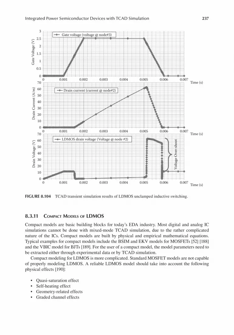
237Integrated Power Semiconductor Devices with TCAD Simulation
8.3.11 compAct models oF ldmos
Compact models are basic building blocks for today’s EDA industry. Most digital and analog IC simulations cannot be done with mixed-mode TCAD simulation, due to the rather complicated nature of the ICs. Compact models are built by physical and empirical mathematical equations. Typical examples for compact models include the BSIM and EKV models for MOSFETs [52] [188] and the VBIC model for BJTs [189]. For the user of a compact model, the model parameters need to be extracted either through experimental data or by TCAD simulation.
Compact modeling for LDMOS is more complicated. Standard MOSFET models are not capable of properly modeling LDMOS. A reliable LDMOS model should take into account the following physical effects [190]:
• Quasi-saturation effect• Self-heating effect• Geometry-related effects• Graded channel effects
3
2.5Gate voltage (voltage @ node#3)
LDMOS drain voltage (Voltage @ node #2)
2
1.5
Time (s)
Dra
in V
olta
ge (V
)D
rain
Cur
rent
(A/m
)G
ate V
olta
ge (V
)
Time (s)
Time (s)
1
0.5
0 0.001 0.002 0.003 0.004 0.005 0.006 0.007
0 0.001 0.002 0.003 0.004 0.005 0.006 0.007
0 0.001 0.002 0.003 0.004 0.005 0.006 0.007Vo
ltage
Ove
r-sh
oot
0
70605040302010
0
70605040302010
0
Drain current (current @ node#2)
FIGURE 8.104 TCAD transient simulation results of LDMOS unclamped inductive switching.

238 Integrated Power Devices and TCAD Simulation
• Bulk current• Impact ionization in the drift region• High-side switch effect• Parasitic BJT effect
Unlike digital and analog MOSFETs, numerous subcircuit models that include MOSFET plus resistors, diodes, capacitors, inductors, and even junction gate field effect transistor (JFETs) are developed for LDMOS [190]. A typical example of such models is shown in Figure 8.105 [191].
Source/Body
D
DrainRD
CGD
J1
M1
CGB
RS
RG
Gate
FIGURE 8.105 A typical subcircuit model for LDMOS.

239
9 Integrated Power Semiconductor Devices with 3D TCAD Simulations
This chapter provides a few 3D technology computer-aided design (TCAD) simulation examples for power semiconductor devices. Since the structure of power devices is getting more and more complex, traditional 2D simulations often fail to reveal important three-dimensional effects. Typical device examples with pronounced three-dimensional effects include Super Junction LDMOS, segmented anode lateral insulated gate bipolar transistor (LIGBT), and complicated interconnect structures.
9.1 3D DEVICE LAYOUT EFFECT
For power devices design, one of the most important considerations is the breakdown voltage. To enhance this value, we need to know how the electric field is distributed in the device: a uniformly distributed electric field is always preferred, but in a real design electric field crowding is unavoidable.
If we take a look at the power LDMOS layout, two of the most frequently used layout structures are given in Figure 9.1. Figure 9.1a has a racetrack layout structure, and Figure 9.1b has a rectangle shaped layout.
When a positive voltage is applied to the N+ drain contact while keeping gate and source/body terminals grounded, the device is reverse biased. For illustration purpose, if we plot the electric field lines, we can see a “flat” portion on both racetrack and square/rectangle shaped structures. The electric field in the flat regions (highlighted in dotted rectangles) resembles the ideal parallel-plane electric field in a power device. The curved regions in the racetrack structure and the corner points in the rectangle shaped structure will modify the electric field distribution and cause crowding of the electric field lines, as seen in Figure 9.2. This field crowding is a 3D effect and will degrade breakdown voltage.
To analyze this 3D field crowding effect, we can use 3D TCAD to simulate simplified structures and observe the distribution of the electric field. We first compare a square shaped structure and a circular shaped structure, with simulation parameters shown in Figure 9.3.
3D net doping plots for both structures are shown in Figures 9.4a and 9.4b; the differential poten-tial is also illustrated in Figures 9.4c and 9.4d. For both devices, 40 V is applied to the cathode, and the anode is grounded.
Comparison plots of electric field magnitude are given in Figure 9.5. Figures 9.5a and 9.5b are 3D electric field plots for the square and circular structures; Figures 9.5c and 9.5d are 3D surface plots (XZ plane at Y = 0) to better visualize the same data. We can see from Figures 9.5c and 9.5d that the square-shaped structure has a higher average electric field than the circular structure. The electric field also peaks at the corners of the device, indicating high electric field crowding.
Further breakdown simulations using the same model parameters are performed for both struc-tures, and the results are shown in Table 9.1. As expected, the higher field values in the square structure correlate with a much lower breakdown voltage than that of the circular structure. We also observe that while the 2D result is consistent with the ideal parallel-plane breakdown result given in (Table 6.6) both 3D structures show a significant deviation from this value. This clearly shows the importance of three-dimensional TCAD simulations.

240 Integrated Power Devices and TCAD Simulation
Regions withparallel-plane
field
(a) Electric field lines in LDMOSwith racetrack shaped layout
(b) Electric field lines in LDMOSwith rectangle shaped layout
FIGURE 9.2 Electric field lines plots for (a) racetrack-shaped layout and (b) rectangle-shaped layout LDMOS.
(b) LDMOS with rectangleshaped layout
Source/Body
Poly Gate
Drain
P+n+Poly
STI
n+
P+n+Poly
STI
n+
(a) LDMOS with racetrackshaped layout
FIGURE 9.1 Two layout structures of LDMOS with (a) racetrack and (b) rectangle.
(b) Square PN junction top down view(a) Circular PN junction top down view
Silicon with borondoping concentration
of 1E+20 cm–3
Silicon with borondoping concentration
of 1E+20 cm–3
Phosphorous (1E+20 cm–3)
D = 16 µm
r = 2 µm
R = 8 µm
d = 5 µm
Phosphorous (1E+20 cm–3)Phosphorous(1E+20)
(1E+20)Phosphorous
(1E+20)Phosphorous
Phosphorous(1E+20)
Z Si
ze =
20
µm
Z Si
ze =
20
µm
X Size = 20 µmX Size = 20 µm
Silicon withphosphorous doping
concentration of5E+15 cm–3
Silicon withphosphorous doping
concentration of5E+15 cm–3
FIGURE 9.3 Simulation structures and parameters for 3D field crowding effect with (a) circular and (b) square.

241Integrated Power Semiconductor Devices with 3D TCAD Simulations
(d) Potential plot of the circular shaped structure(c) Potential plot of the square shaped structure
(a) Net doping plot of the square shaped structure
3D Net Doping and Potential (40 V) Plot: Circular and Square Shapes
(b) Net doping plot of the circular shaped structure
FIGURE 9.4 3D simulation results with net doping plots of (a) square and (b) circular structures and poten-tial plots of (c) square and (d) circular structures.
300000
500000
Elec Field Mag.(V/cm)
Elec Field Mag.(V/cm)
Elec Field Mag.(V/cm)
Elec Field Mag.(V/cm)
Elec Field Mag.(V/cm)
3D Electric Field Comparison: Circular and Square Shapes
Elec Field Mag.(V/cm)
450000400000350000300000300000
250000
200000
150000
100000
50000
0
250000200000150000100000
500000
450000400000350000300000250000200000150000100000500000
1520+X
+X10 5 0 0
1015
40000035000030000025000020000015000010000050000 20 15 10 5
0 05
1015
20+Z
+Z
0
500000450000400000350000300000250000200000150000100000
500000
2015
105
0 05
1015
20
x(micron)y(micron)
2015
10
5
0 05
1015
20y(micron)
x(micron)
250000
200000
150000
100000
50000
(d) Surface plot of electric field of circularshaped structure (XZ plane at Y = 0)
(c) Surface plot of electric field of squareshaped structure (XZ plane at Y = 0)
(a) Electric field plot of the squareshaped structure
(b) Surface plot of electric field of circularshaped structure (XZ plane at Y = 0)
0
FIGURE 9.5 3D simulation results with electric field plots of (a) square and (b) circular structures and sur-face plot of electric field of (c) square and (d) circular structures.

242 Integrated Power Devices and TCAD Simulation
The potential plots at breakdown for all three structures are given in Figure 9.6 for (a) the circular structure and (b) square-shaped structure. A 2D XY cut at Z = 10 µm (center) of the square-shaped structure is also shown in Figure 9.6c.
9.2 3D SIMULATION OF LIGBT
9.2.1 ABout ligBt
As we already know, the on-resistance of an LDMOS increases with higher breakdown voltage due to conflicting requirements regarding low doping in the drift region. For breakdown voltages higher than 600 V, an LDMOS, even a Super Junction LDMOS, exhibits a very high on-resistance. The insulated gate bipolar transistor (IGBT) structure was invented in the 1980s for high-voltage and high-current applications; its lateral version, LIGBT, was created by engineers for power integrated circuit applications (as discussed in Chapter 4). The merit of LIGBT over LDMOS is the signifi-cantly lower on-state resistance for high voltage designs, thanks to the plasma injection of minority carriers when the LIGBT is turned on.
In terms of device structure, LIGBT is very similar to an LDMOS with a gate-controlled MOS structure and a long lightly doped drift region to support high voltages. However, LIGBT has an extra P+/N junction at the anode (or collector) side, which differentiates it from an LDMOS. Figure 9.7 illustrates a comparison between LDMOS (Figure 9.7a) and LIGBT (Figure 9.7b). In the
TABLE 9.1Comparison of Breakdown Simulation Results
Simulated StructuresSimulated
Breakdown VoltageDeviation from 2D Breakdown Voltage
3D circular shape 67 V –26%
3D square shape 50 V –45%
2D cut from square shape 91 V 0%
(c) Potential plot at breakdown of 2D simulation(2D XY plane at Z = 10 um from the square shaped structure)
(a) Potential plot at breakdownof circular shaped structure
Potential Plots at Breakdown: Circular, Square and 2D Structure
Differential Potential
Differential Potential
Differential Potential67.1147605040302010 20
+X
15 10 5 0
0
91.55469080706050403020100
5 10
BV = 91 V
15 20
05
10BV = 67 VBV = 50 V
1520
50.122750403020
20+X
1510 5 0 0
510
1520+Z
100
+Z
0
(b) Potential plot at breakdownof square shaped structure
FIGURE 9.6 The potential plots at breakdown of (a) circular shape, (b) square shape, and (c) 2D plane (XY plane at Z = 10 µm of the square-shaped structure).

243Integrated Power Semiconductor Devices with 3D TCAD Simulations
LIGBT structure, a P+ anode replaces the N+ drain of the LDMOS, and the identical source/body in the LDMOS is now called the cathode.
9.2.2 segmented Anode ligBt
LIGBT is promising for high-power applications in smart power ICs, thanks to the much lower on-resistance resulting from conductivity modulation of the high-resistivity drift region by injection of minority carriers. Unfortunately, this minority carrier injection also causes minority carrier storage effects, which substantially degrade the device switching speed. A shorted anode N+ device was pro-posed to alleviate this problem by providing an electron extraction path incorporated at the anode to extract electrons during device turnoff, the structure of which is illustrated in Figure 9.8. With access to the electrons, the electron–hole plasma in the drift region can be extracted, and a significant improve-ment in switching speed with only moderate decrease in current handling capability compared to the P+ anode [105]. This improvement is due to the incorporation of the N+ diffusion at the anode, which helps in removing the plasma during device turnoff. However, the continued forward bias of the anode dur-ing device turnoff, which causes unnecessary minority-carrier injection, retains the turnoff time of the
(a) LDMOS structure (b) LIGBT structure
P-substrateP-substrate
N-epi N-epi
LOCOSLOCOS
AnodeCathodeSource/Body Drain
P-chanP-chan
P-isoP-iso
P+ P+N+P+ N+ N+GateGate
FIGURE 9.7 Comparison between the LDMOS structure and LIGBT structure.
Cathode
Gate
Anode
P+ N+N-epi
LOCOS
P-substrate
P-chan
PBLP-iso
P+ N+
FIGURE 9.8 Schematic view of LIGBT with PBL and shorted anode N+ region.

244 Integrated Power Devices and TCAD Simulation
device in the order of hundreds of nanoseconds [192]. Also, the additional area required for implement-ing the anode N+ diffusion makes the device less area-efficient.
For the shorted anode structure, the injection efficiency of the P+/N+ anode depends on the P+ length for a constant N+ length. For good injection efficiency, a large P+ length is needed; however, this will slow down the switching speed due to the overinjection during on-state and excessive injec-tion during device turnoff. Furthermore, the device size will be increased due to the large anode size. On the other hand, a faster device can be achieved by reducing the P+ length. The maximum speed of the device is limited by the practical minimum of the P+ length [192].
A smart structure called segmented anode LIGBT was proposed in [193]. A simplified 3D sche-matic view of this segmented anode LIGBT is shown in Figure 9.9. This design eliminates the problems of long anode length and excessive hole injection during device turnoff. In this structure, the electron conduction path at the anode is implemented along the device width by periodically eliminating part of the P+ diffusion and replacing it with an N+ diffusion. Since the anode is imple-mented using segments of P+ and N+ diffusions, it is named as segmented anode LIGBT. At low forward bias, electrons that flow from the channel through the drift region are collected by the anode N+ diffusion in a way identical to that of the LDMOS. At high forward bias, the P+ portion of the anode, which is situated in parallel with the N+ diffusion, is turned on. The turn-on is caused by the voltage developed in the drift region due to the electron flow from the channel to the anode. Turning on of the P+ injector injects minority carriers into the drift region. These minority carriers modulate the drift region resistivity and provide a low on-resistance.
During the on-state, the electron and hole current flow paths are similar to that of the shorted anode LIGBT. However, during the turnoff transient, most electrons in the segmented anode structure flow directly from the drift region and the substrate to the N+ region without flowing underneath the P+ diffusion as different from the case of the shorted anode device. Therefore, no continued turn-on of the anode exists during the turnoff transient. The electrons present in this structure are extracted through the anode N+ diffusion and the holes are extracted through the P+ cathode for fast device turnoff.
The segmented anode design provides the following advantages. First, this device requires a smaller anode area compared to that of the shorted anode LIGBT. This is because the N+ diffu-sion, which is located behind the P+ anode diffusion in the shorted anode LIGBT, is not needed, and the area needed by the N+ diffusion at the anode of the segmented anode LIGBT is relatively small. The smaller anode area makes the device more area-efficient despite the fact that part of the P+ anode area is used for implementing the N+ diffusion. Second, faster switching speed can be achieved compared to the shorted anode device for the same current handling capability. This is because the N+ diffusion in the segmented anode design is located in parallel with the P+ diffusion instead of behind the P+ diffusion as in the case of the shorted anode design. Most of
P-Substrate
N-epiGate
N+P+
P+
N+
FIGURE 9.9 3D schematic view of segmented LIGBT.

245Integrated Power Semiconductor Devices with 3D TCAD Simulations
the electrons that are extracted from the drift region can flow to the anode N+ diffusion without flowing underneath the P+ diffusion. Only a small amount of electrons that flow near the two ends of the P+ injector will cause that part of the injector to turn on. This minimizes the forward bias of the P+ injector caused by electron extraction during device turnoff, resulting in faster switching speed compared with the shorted anode design. Finally, the trade-off between the on-resistance and the turnoff time can be achieved simply by adjusting the ratio of the P+ to N+ diffusion width along the device width. The wider the P+ diffusion, the lower the on-resistance and the longer the device turnoff time will be for a constant N+ diffusion width. Whereas in the case of the shorted anode LIGBT, increasing the P+ anode length for lower on-resistance may have to increase the device area as the P+ anode length is made longer [105].
9.2.3 3d process simulAtion oF segmented Anode ligBt
Since the segmented anode LIGBT can be revealed only with 3D simulations, both 3D process simulation and device simulation are performed for better understanding of the device physics. Nine masks are used to create the LIGBT structure: P-type buried layer (PBL); local oxidation of silicon (LOCOS); P-iso; P-body; gate, N-plus; P-plus; contact; and Metal1. The device width is 25 µm: P+ anode occupies 20 µm, and N+ anode takes 5 µm. The total cell pitch of the device is 45 µm. The layout views of the nine masking steps are provided in Figure 9.10.
The simplified process steps of the segmented anode LIGBT are shown in Figure 9.11, with detailed information given in Table 9.2. In this process, LOCOS is used instead of STI. N-epi is grown on P-substrate, with a thickness of 6.5 µm. PBL mask and implant are utilized. The RESURF (Reduced Surface Electric Field) implant is a blanket implant to adjust the doping concentration in the N-epi layer. The P-ISO and drive-in step is applied so that a deep and heavily doped P+ region connects the P-body to the P-substrate. P+ and N+ sections coexist in the anode region and are self-aligned to the LOCOS. In this particular simulation example, P+ has a width of 20 µm, while N+
PBLLOCOSP-ISOP-bodyGateN-plusP-plusContactMetal1
PBLLOCOSP-ISOP-bodyGateN-plusP-plusContactMetal1
PBLLOCOSP-ISOP-bodyGateN-plusP-plusContactMetal1
PBLLOCOSP-ISOP-bodyGateN-plusP-plusContactMetal1
(d) PBL+LOCOS+P-ISO+P-body+Gate+N-plus+P-plus+Contact+Metal1
(c) PBL+LOCOS+P-ISO+P-body+Gate+N-plus+P-plus
(a) PBL+LOCOS (b) PBL+LOCOS+P-ISO+P-body
FIGURE 9.10 Layout views of the segmented anode LIGBT.

246 Integrated Power Devices and TCAD Simulation
TABLE 9.2Simplified Process Steps of 3D TCAD Simulation of a Segmented Anode LIGBTProcess Steps Description1. P-sub Boron concentration of 3E+14 cm-3, orientation = (100)
2. PBL mask Apply PBL photomask (negative mask, photoresist is removed where the patterns are drawn)
3. PBL implant Boron implant with dose = 2E+12 cm-2, energy = 120 keV
4. PBL anneal 1 minute thermal anneal at temperature of 1000°C
5. N-epi layer N-type epitaxial layer with thickness of 6.5 µm is deposited. The phosphorus doping concentration is 5E+14 cm-3
6. RESURF implant Phosphorus blanket implant with dose = 1.5E+12 cm-2, energy = 150 keV
7. RESURF anneal 1 minute thermal anneal at temperature of 1000°C
8. Pad oxide Pad oxide of 0.02 µm
9. Nitride deposit Silicon Nitride (Si3N4) deposition with thickness of 0.3 µm
10. LOCOS mask Apply LOCOS photomask (negative mask, photoresist is removed where the patterns are drawn)
11. Nitride etch Nitride is etched where unmasked
12. LOCOS growth 60 minutes wet oxide at temperature of 1000°C
13. Etch nitride Excessive nitride is etched away (thick = 0.3 µm)
14. Oxide etch Excessive oxide is etched away (thick = 0.02 µm)
15. P-iso mask Apply P-iso photomask (negative mask, photoresist is removed where pattern is drawn)
16. P-iso implant Boron implant with dose = 1.5E+16 cm-2 and energy = 150 keV
17. P-iso drive-in 100 minute thermal drive-in at temperature of 1150°C
18. P-body mask Apply P-body photomask (negative mask, photoresist is removed where the patterns are drawn)
19. P-body implant Boron implant with dose = 3E+13 cm-2, energy = 50 keV
20. P-body drive-in 120 minute thermal drive-in at temperature of 1150°C
21. Gate oxide Gate oxide growth to yield oxide thickness of 600 Å
22. Poly deposition Polysilicon deposition of 0.4 µm with phosphorus concentration of 1E+20 cm-3
23. Gate mask Apply gate photomask (positive mask, photoresist is preserved where the patterns are drawn)
24. Gate etch Polysilicon and oxide are subsequently dry-etched
25. Gate anneal Poly gate anneal at 1150°C for 1 minute
26. N-plus mask Apply N-plus photomask (negative mask, photoresist is removed where the patterns are drawn)
27. N-plus implant Phosphorus implant with dose = 2E+16 cm-3 and energy = 20 keV
28. N-plus anneal Thermal anneal for 10 seconds at 900°C
29. P-plus mask Apply P-plus photomask (negative mask, photoresist is removed where the patterns are drawn)
30. P-plus implant Boron implant with dose = 1E+16 cm-3 and energy = 15 keV
Metal1ContactsP-plusN-plus
Gate
P-sub PBL N-epi RESURF
P-body P-iso LOCOS
FIGURE 9.11 Simplified process steps of 3D TCAD simulation of a segmented anode LIGBT.

247Integrated Power Semiconductor Devices with 3D TCAD Simulations
has a width of 5 µm. We will make a comparison between different P+ to N+ ratios later in terms of forward and turnoff transit characteristics.
The process simulation results are given in Figure 9.12 with material plot and net doping plots. For a better view of net doping in silicon, all other materials except silicon are ripped off in Figure 9.12c to expose silicon only. A 2D cut of XY plane at Z = 0 (with P+ anode) is also shown in Figure 9.12d.
TABLE 9.2 (CONTINUED)Simplified Process Steps of 3D TCAD Simulation of a Segmented Anode LIGBT
Process Steps Description31. P-plus anneal Thermal anneal for 10 seconds at 900°C
32. Oxide deposition
Deposit oxide with thickness of 0.5 µm
33. Contact mask Apply contact photomask (negative mask, photoresist is removed where the patterns are drawn)
34. Contact etch Etch oxide to expose contact locations
35. Metal deposition Deposit metal with thickness of 0.7 µm
36. Metal mask Apply metal photomask (positive mask, photoresist is preserved where the patterns are drawn)
37. Metal etch Etch metal to leave cathode, gate, and anode contacts
(d) 2D net doping plot of segmented LIGBTshowing P+ anode
(c) Net doping plot of segmented LIGBTwith silicon material only
(a) Material plot of segmented LIGBT
Material Number
4045+X
+X
35 30 25 20 15 10 5 0
404535 30 25 20 15 10 5 0 0
5 1015
2025+Z
0 5 1015
20 354045+X
30 25 20 15 10 5 0 0 5 1015
2025
+Z
–20–15–10–505
101520
Net_Doping
–20–15–10–505
101520
Net_Doping
25
+ZAl
Si
SiO2Poly
Segmented LIGBT
(b) Net doping plot of segmented LIGBT
FIGURE 9.12 Simulation results of segmented anode LIGBT with (a) material plot, (b) net doping plot, (c) net doping plot with silicon material only, and (d) 2D net doping plot showing a P+ anode.

248 Integrated Power Devices and TCAD Simulation
9.2.4 3d device simulAtion oF segmented Anode ligBt
9.2.4.1 Forward Characteristic SimulationSince the breakdown characteristic of the segmented anode LIGBT is similar to LDMOS, the break-down analysis will not be repeated here. Forward characteristics of segmented anode LIGBT are analyzed at different P+ anode to N+ anode section ratios, with the following simulation conditions:
1. Gate voltage is first biased to 5 V to ensure the device is fully turned on. 2. Anode voltage is scanned to 1.5 V followed by a current scan till the anode current reaches
0.004 A. (With 45 µm by 25 µm device size, this current density is about 360 A/cm2.)
The simulation results of different P+ anode to N+ anode ratios are compared in Figure 9.13. N+ only structure (LDMOS) has the highest on-resistance and no minority carrier injection effect. With higher ratio of P+ section over N+ section in the anode, higher current handling capability is obtained with the same anode voltage. P+ only (pure LIGBT) has the highest current handling capability and the lowest on-resistance.
In comparison with pure P+ anode LIGBT, which has an onset voltage (P+/N– junction turn-on voltage) of less than 1 V, for segmented anode LIGBT there is a voltage clamping effect at the P+/N+ anode. The N+ region clamps the voltage near the anode such that the P+/N– diode does not turn on at a low forward bias; it behaves like a resistor with electrons flowing from the cathode through the N- region to the N+ anode. Before the injector turns on, electrons accumulate at the P+/N– junction situated away from the anode N+ region, which reduces the potential at the N– region and increases the bias across that part of the junction. At a higher forward bias, voltage developed across the P+/N– junction eventually turns on the junction. In other words, lateral flow (in the third dimension) of electrons under the P+ anode diffusion to the N+ anode diffusion, producing lateral Ohmic drops, is the mechanism by which the P+/N– junction in the segmented anode LIGBT structure becomes forward biased. After the junction is forward biased, minority carriers are injected into the N– region to conductivity-modulate the drift region resistance. Thus, holes are injected from the P+ anode into the N– region. Many fewer holes are observed in the N– region underneath the N+ anode due to the voltage clamping effect at the P+ injector near the N+ diffusion. Since the conductivity modulation effect reduces the drift region
5.04.0 4.5
N+ onlyP+ onlyP+=12.5 um & N+=12.5 umP+=15 um & N+=10 umP+=20 um & N+=5 umP+=22.5 um & N+=2.5 umP+=24 um & N+=1 um
3.53.02.5Anode Voltage (V)
Ano
de C
urre
nt (A
)
1.51.00.50.00.0000
0.0005
0.0010
0.0015
0.0020
0.0025
0.0030
0.0035
0.0040
2.0
FIGURE 9.13 Forward I-V curves of different anode P+/N+ ratios.

249Integrated Power Semiconductor Devices with 3D TCAD Simulations
resistance, forward voltage of the device after the injector turns on is actually lower than the forward voltage before the injector turns on and at a much higher forward current.
The simulated I-V characteristics of the segmented anode LIGBT with different anode P+ to N+ ratio are illustrated in Figure 9.13. Except anode cases with P+ only (pure LIGBT) and N+ only (LDMOS), the segmented anode LIGBTs exhibit bistable I-V characteristics with two conduction regimes. The bistable characteristic, as will be described shortly, is due to the conductivity modula-tion effect coupled with an Ohmic voltage drop developed at the electron conduction path imple-mented by the anode N+ diffusion. The first conduction regime represents the LDMOS conduction regime, in which the forward bias is so low that the P+/N– diode at the anode is not active, and the current flow is taking place at the anode N+ diffusion. At a high forward bias, the voltage developed across the diode causes the diode to turn on and conductivity-modulates the drift region shunting resistance, which shunts the current flowing into the P+/N– junction. Since the shunting resistance drops after the P+/N– diode turns on, the forward voltage drops correspondingly, even at a higher current density. This causes the I-V characteristic to snap back. As the conductivity modulation effect is saturated, further increase in current level causes the forward voltage to increase, and the I-V characteristic reaches the bipolar regime. The voltage at which the snapback starts to occur is defined as the onset voltage, Vonset. The Vonset is adjustable and is a function of the shunting resistance. The lower the shunting resistance, the higher the Vonset. Since the shunting resistance is partially determined by the anode P+ to N+ ratio, the onset voltage and the level of conductivity modulation can then be determined by adjusting the P+ to N+ ratio. The smaller P+ to N+ ratio rep-resents a smaller shunting resistance, which allows more current to flow through before the diode turns on and therefore results in a higher onset voltage. This higher onset voltage translates into a higher forward voltage and gives rise to a lower current handling capability compared with a larger P+ to N+ ratio. Thus, by adjusting the P+ to N+ ratio, a different injection efficiency can be achieved and segmented anode LIGBTs can be designed to have different current handling capability [193].
Except the N+ structure (LDMOS), with anode voltage passes some onset voltage (Vonset), elec-tron–hole plasma is formed in the drift region, which modulates the conductivity of the drift region and lowers the on-resistance of the transistor, as mentioned before. Figure 9.14 is the 3D TCAD simulation results of a segmented anode LIGBT with P+ (20 µm) and N+ (5 µm). We can see the electron–hole plasma in 3D from Figure 9.14 and in 2D cut planes from Figure 9.15. At a forward voltage of 1.75 V and a forward current of 0.002 A (after snapback), it is evident that very high electron and hole concentrations are located at the anode side of the drift region and that relatively
25+Z
2015
105
005
0 0.005
Hole_Conc (E18/cm3)Elec_Conc (E18/cm3)
0.01 0.015 0.02 0.030.025 0.035 0.04 0.050.0450 0.005 0.01 0.015 0.02 0.030.025 0.035 0.04 0.050.045
101520
(b) Hole Concentration @ Ia = 0.002A(a) Electron Concentration @ Ia = 0.002A
30354045
Segmented LIGBT Electron and Hole Concentrations @ Ia = 0.002 A
+X
25
25+Z
2015
105
00510152030354045
+X
25
FIGURE 9.14 3D simulation results of electron and hole plasma injection of segmented anode LIGBT at Ia = 0.002 A (P+ = 20 µm and N+ = 5 µm).

250 Integrated Power Devices and TCAD Simulation
lower concentrations are located at the cathode side of the drift region. Ideally, we would like to see a more uniform plasma concentration in the entire drift region for a low on-state resistance. Figures 9.14 and 9.15 show that the current design of the device does not have an optimized plasma distribution profile as far as conductivity modulation of the drift resistivity is concerned. A more optimum design of the plasma profile should have the amount of holes injected by the anode to be reduced (for faster switching as will be discussed in the next section) and the amount of electrons injected by the cathode to be increased (for attracting more holes to flow to the cathode side of the drift region for further conductivity modulation).
As described already, hole injection can be reduced by adjusting the P+/N+ ratio at the anode or by implementing the anode using a Schottky contact, which was first introduced to minimize the anode hole injection in the LIGBT. This device was called the Schottky injection field effect transistor (SINFET) [194]. A lightly doped P anode was also used later on to reduce the hole injection in the IGBT [195]. This structure also allows a lighter N-buffer region to be used to produce a field stop IGBT (FS IGBT) for a more optimum switching loss performance. Electron injection enhancement can be done by increasing the resistive path for holes flow to the cathode using a narrow mesa trench gate structure [196]. With a pair of deep trenches and a narrow N-mesa, accumulation of holes at the narrow mesa raises the elec-trostatic potential at the P-body/N-drift junction for enhancement of electron injection from the channel. This much increased electron–hole plasma concentration at the cathode side of the N-drift is responsible
4502468
101214161820222425
02468
101214161820222425
02468
10 Anode
LOCOS Region
P-bo
dy/
P-iso
Chan
el
N+
LOCOS Region
Net dopingXZ plane cut @ Y = 6.5 µm(Silicon surface)
Electron Concentration@ Ia = 0.002AXZ plane cut @ Y = 6 µm(0.5 µm below silicon surface)
Hole Concentration@ Ia = 0.002AXZ plane cut @ Y = 6 µm(0.5 µm below silicon surface)
P+
N+
Segmented LIGBT Electron and Hole Concentrations at Forward Bias
1214161820222425
43 41 39 37 35 33 31 29 27 25 23 21 19 17 15 13 11 9 8 7 6 5 4 3 2 1 0
45 43 41 39 37 35 33 31 29 27 25 23 21 19 17 15 13 11 9 8 7 6 5 4 3 2 1 0
45 43 41 39 37 35 33 31 29 27 25 23 21 19 17 15 13 11 9 8 7 6 5 4 3 2 1 0
Net_Doping
XZ plane Y=6.5 um20
15
10
5
0
–5
–10
–15
–20
Accu
mul
atio
n
Plot location onthe I-V curve
Plot location onthe I-V curve
+X+Z
0.05
3.21899e-0151234567899.16449
Hole_Conc (E18/cm3)
Elec_Conc (E18/cm3)
0.0450.040.0350.030.0250.020.015
0.0050
0.01
FIGURE 9.15 XZ plane at Y = 6 µm plots with net doping, hole concentration, and electron concentration of segmented anode LIGBT at Ia = 0.002 A (P+ = 20 µm and N+ = 5 µm).

251Integrated Power Semiconductor Devices with 3D TCAD Simulations
for the further reduction of the on-resistance in the structure. With this increase in plasma, the entire drift region is now conductivity modulated for the optimum on-state performance.
9.2.4.2 LIGBT Turnoff Transient SimulationThe turnoff transient of the segmented anode LIGBT can be simulated with a resistive load; the simulation setup is illustrated in Figure 9.16. A resistor of 50 KΩ is connected in series to the anode of the LIGBT. The simulation procedure is as following:
1. Equilibrium is first established. 2. Gate voltage is scanned to 5 V in 10 μs. 3. Anode voltage is scanned to 1 V in 10 μs. 4. Anode current is scanned to 0.002 A in 10 μs (178 A/cm2 in anode current density, the
voltage on Node #1 of Figure 9.16 should reach approximately 100 V). 5. Turn off the LIGBT by rapidly ramping down the gate voltage from 5 V to 0 V in 7 ns. 6. Scan the time till the anode current decreases to a negligible level.
The transient simulation results of the LIGBT turnoff are illustrated in Figure 9.17. Note that compared with the N+ only and other segmented anode LIGBTs, the P+ only configuration takes too long for the current to drop to a negligible level; therefore, it is drawn in a separate curve in Figure 9.18. The long turnoff time of the P+ only LIGBT is expected, since the minority carriers injected when the anode is forward biased is not possible to be extracted with a P+ only anode. Removal of the electron–hole plasma for device turnoff can be relied only on electron–hole recombination, which is mainly a function of the minority carrier lifetime. The stored minority carriers prevent the transistor to switch fast. With even a small N+ region, the switching time decreases significantly. The switching time can be adjusted by modifying the P+/N+ ratio: the smaller the ratio, the shorter the turnoff time, with the N+ only (LDMOS) being the extreme case.
Unfortunately, as we have observed in Figure 9.13, under the forward bias condition, a smaller P+/N+ ratio means lower current handling capability (higher on-resistance). A trade-off has to be made between fast switching and current handling capability (on-resistance).
The electron and hole plasma distributions in the segmented anode LIGBT structure (P+ = 20 µm and N+ = 5 µm) during turnoff transient are shown in Figures 9.19 and 9.20, respectively. In
LIGBT
Gate Control:5 V -> 0 V in 7 ns
Node #2(Anode)
R = 50 KΩ
Node #1Initial
Ia = 0.002 A
VDD = 100 V
+–
FIGURE 9.16 Circuit setup of LIGBT turnoff transient simulation.

252 Integrated Power Devices and TCAD Simulation
Figure 9.19, one can see that electrons at the cathode region are removed almost instantly after the removal of the MOS channel in approximately the first 10 ns into turnoff. This causes the sudden drop of the anode current in the first 10 ns, as shown in the I-V curve in Figure 9.17. As the device gets deeper into turnoff, the electron plasma was removed through electron–hole recombination in the drift region as well as electron extraction through the anode (at time = ~35 ns), in which the
P+ only LIGBT turnoff transient
Time (nS)
Ano
de C
urre
nt (A
)
4000 8000 12000 16000 20000 24000 28000 32000 36000 400000
0.0002
0.0000
0.0004
0.0006
0.0008
0.0010
0.0012
0.0014
0.0016
0.0018
0.0020
LIGBT Turnoff with Switch Voltage = 100 V and Current = 178 A/cm2
(Gate switch off time = 7 ns)
FIGURE 9.18 Turnoff transient simulation results of LIGBT with P+ only anode.
320
P+=24 um & N+ = 1 umP+=22.5 um & N+ = 2.5 umP+=20 um & N+ = 5 umP+=15 um & N+ = 10 umP+=12.5 um & N+ = 12.5 um
N+ onlyP+ only
300280260240220200180160Time (nS)
Ano
de C
urre
nt (A
)
140120100806040200
0.0002
0.0004
0.0006
0.0008
0.0010
0.0012
0.0014
0.0016
0.0018
0.0020
LIGBT Turnoff with Switch Voltage = 100 V and Current Density = 178 A/cm2
(Gate switch off time = 7 ns)
FIGURE 9.17 Turnoff transient simulation results of segmented anode LIGBTs.
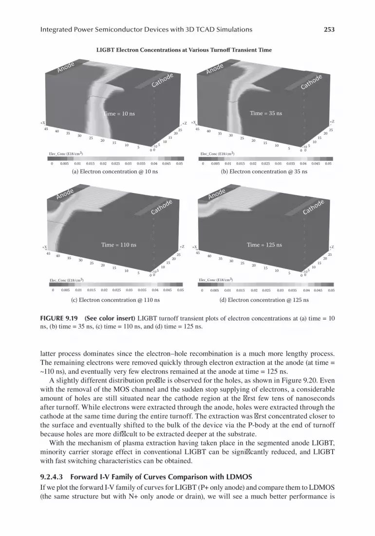
253Integrated Power Semiconductor Devices with 3D TCAD Simulations
latter process dominates since the electron–hole recombination is a much more lengthy process. The remaining electrons were removed quickly through electron extraction at the anode (at time = ~110 ns), and eventually very few electrons remained at the anode at time = 125 ns.
A slightly different distribution profile is observed for the holes, as shown in Figure 9.20. Even with the removal of the MOS channel and the sudden stop supplying of electrons, a considerable amount of holes are still situated near the cathode region at the first few tens of nanoseconds after turnoff. While electrons were extracted through the anode, holes were extracted through the cathode at the same time during the entire turnoff. The extraction was first concentrated closer to the surface and eventually shifted to the bulk of the device via the P-body at the end of turnoff because holes are more difficult to be extracted deeper at the substrate.
With the mechanism of plasma extraction having taken place in the segmented anode LIGBT, minority carrier storage effect in conventional LIGBT can be significantly reduced, and LIGBT with fast switching characteristics can be obtained.
9.2.4.3 Forward I-V Family of Curves Comparison with LDMOSIf we plot the forward I-V family of curves for LIGBT (P+ only anode) and compare them to LDMOS (the same structure but with N+ only anode or drain), we will see a much better performance is
(d) Electron concentration @ 125 ns
(b) Electron concentration @ 35 ns
Time = 35 nsTime = 10 ns
(c) Electron concentration @ 110 ns
(a) Electron concentration @ 10 ns
LIGBT Electron Concentrations at Various Turnoff Transient Time
0.050.0450.0350.030.0250.0150.005
Elec_Conc (E18/cm3)Elec_Conc (E18/cm3)
Elec_Conc (E18/cm3) Elec_Conc (E18/cm3)
0 0.020.01
303540
4525
+Z +X
2015
105
0
2520
1510
500
051015
2025
Time = 110 ns Time = 125 ns
30354045
51015202530354045
+X
+X
25 2015 10 5 0 0
510
1520
25
+Z
30354045
+X+Z
25 20 15 105 0 0
510
1520
25
+Z
0.040.050.0450.0350.030.0250.0150.0050 0.020.01 0.04
0.050.0450.0350.030.0250.0150.0050 0.020.01 0.04 0.050.0450.0350.030.0250.0150.0050 0.020.01 0.04
FIGURE 9.19 (See color insert) LIGBT turnoff transient plots of electron concentrations at (a) time = 10 ns, (b) time = 35 ns, (c) time = 110 ns, and (d) time = 125 ns.

254 Integrated Power Devices and TCAD Simulation
obtained with the LIGBT structure, except for a tiny region before the onset of injection at low anode (or drain) voltage, as shown in Figure 9.21.
9.3 SUPER JUNCTION LDMOS
9.3.1 BAsic concept
Like RESURF, which employs a charge coupling effect, a Super Junction LDMOS uses alternating N- and P-regions to mutually deplete each other so that a higher doping concentration and lower on-resistance can be achieved. It also means that for the same doping concentration in the drain-drift region, a higher breakdown voltage can be obtained.
To explain the Super Junction concept, we start with a simple 2D simulation. In Figure 9.22, a simple 2D structure with alternating N- and P-pillars is shown. These are used to mimic the N- and P-stripes in the drain-drift region of a Super Junction LDMOS. (In this chapter, we do not distinguish between N/P pillars, N/P stripes, and N/P wells as long as they have alternating N- and P-regions to mutually deplete each other to support high breakdown voltages). Assuming the width of N-pillars equals P-pillars ( ),W WN P= L is the length of N/P pillars. This 2D structure has a
(d) Hole concentration @ 125 ns
(b) Hole concentration @ 35 ns
Time = 35 nsTime = 10 ns
(c) Hole concentration @ 110 ns
(a) Hole concentration @ 10 ns
LIGBT Hole Concentrations at Various Turnoff Transient Time
0.050.0450.0350.030.0250.0150.005
Hole_Conc (E18/cm3)Hole_Conc (E18/cm3)
Hole_Conc (E18/cm3) Hole_Conc (E18/cm3)
0 0.020.01
3035404525
+Z +X
2015
105
0
2520
1510
500
0510152025
Time = 110 ns Time = 125 ns
30354045
51015
2025303540
45
+X
+X
2520 15 10 5 0 0
510
1520
25
+Z
30354045
+X+Z
25 20 1510 5 0 0
510
1520
25
+Z
0.040.050.0450.0350.030.0250.0150.0050 0.020.01 0.04
0.050.0450.0350.030.0250.0150.0050 0.020.01 0.04 0.050.0450.0350.030.0250.0150.0050 0.020.01 0.04
FIGURE 9.20 (See color insert) LIGBT turnoff transient plots of hole concentrations at (a) time = 10 ns, (b) time = 35 ns, (c) time = 110 ns, and (d) time = 125 ns.

255Integrated Power Semiconductor Devices with 3D TCAD Simulations
heavily doped N+ cathode (to mimic the N+ drain contact in Super Junction LDMOS) and a heavily doped P+ anode (to mimic the P-body and the source/body contact).
For this kind of alternating N/P structure, it has been found that the maximum breakdown voltage takes place with maximum (critical) electric field EC at the optimum charge Qopt in the N- and P-regions [158]:
Q qN W qN W Eopt D N P P s C= = = ε (9.1)
where εs = 11.68 is the dielectric constant of silicon, q = 1.602E-19 C is the electron charge, and ND and NP are the doping concentrations of the N- and P-regions, respectively. If we assume EC = 3E + 5 V/cm, the optimum charge Qopt is found to be 3.1E-7 C/cm2. It is often more convenient to use optimum dopant density per unit area (dose = NDWN, which is calculated to be 1.94E + 12 cm-2) than an optimum charge, but this should not be confused with the device implant dose. Following the axis convention used throughout this book, the unit area for the dopant density is defined on the XY plane (along the N/P boundary in this case), while the implant dose is defined on the XZ plane (the wafer surface, perpendicular to XY plane). This optimum charge/dose is often oversimplified and not suitable for cases where depletion is from multiple sources (like double RESURF or multiple RESURF).
9.3.1.1 How to Choose the Pillar Width WN
The N/P pillars widths WN and WP are often designed to be equal to each other, with their values critical for a successful design of Super Junction LDMOS. 2D simulations with different doping concentrations and pillar widths for the simple structure of Figure 9.22 were performed. Different pillar widths were chosen (WN = 0.1, 0.2, 0.3, and 0.4 µm), coupled with different doping concen-trations. Note that during every simulation, WN = WP and doping concentration in N-pillars always equals P-pillars to keep dose balanced. Figure 9.23 shows the simulation results.
For each pillar width, there is an optimum doping concentration, beyond which the breakdown voltage drops dramatically. In general, narrower pillars yield a higher optimum doping concentration,
Anode (Drain) Voltage (V)
IV Curves: LIGBT (P+ Anode) vs. LDMOS (N+ Drain)
00.000
0.001
0.002
0.003
0.004
0.005
0.006
Ano
de (D
rain
) Cur
rent
(A)
0.007
0.008
0.009
0.010LIGBT (P+ anode) Vg = 1LIGBT (P+ anode) Vg = 2LIGBT (P+ anode) Vg = 3LIGBT (P+ anode) Vg = 4LIGBT (P+ anode) Vg = 5LDMOS (N+ drain) Vg = 1LDMOS (N+ drain) Vg = 2LDMOS (N+ drain) Vg = 3LDMOS (N+ drain) Vg = 4LDMOS (N+ drain) Vg = 5
1 2 3 4 5 6 7 8 9 10 11 12 13 14 15 16 17 18 19 20
FIGURE 9.21 The I-V curve comparison between LIGBT (P+ anode) and LDMOS (N+ drain) with the same structure except anode (drain) dopant type.

256 Integrated Power Devices and TCAD Simulation
as predicted by the theory. However, depending on process technology, narrow pillars, like the one with a width of only 0.1 µm, is difficult to obtain with current smart power IC technology. In the near future, with smart power IC feature sizes below 90 nm node, this layout width should be realized.
To better understand how the Super Junction concept works, two simulations are compared. Both structures have N/P pillars doping concentration of 1E + 17 cm-3 but have different pillar widths: as illustrated in Figure 9.24, one device has WN = WP = 0.1 µm, while the other has WN = WP = 0.4 µm. Voltage is applied to the cathode terminals while keeping anode terminals grounded.
The breakdown simulation results for the 0.1 µm device are shown in Figure 9.25. The breakdown voltage for this structure reaches 104 V (Figure 9.25a) and both N- and P-pillars are fully depleted as can be seen from the space charge plot in Figure 9.25b. The electric field is very uniform across the device as shown in Figures 9.25c and 9.25d. The heavily doped N+ cathode and P+ anode regions are excluded in the 3D surface electric field plot of Figure 9.25d.
The breakdown simulation results for the 0.4 µm structure are shown in Figure 9.26. The break-down voltage is limited to 36 V (Figure 9.26a), and the N/P pillars are not fully depleted, as can be
1E1610203040506070
Brea
kdow
n Vo
ltage
(V)
8090
100110120
2D Test Structure Simulation for Super Junction eory
1E17
Wn = Wp = 0.4 umWn = Wp = 0.3 umWn = Wp = 0.2 umWn = Wp = 0.1 um
N/P Pillars Doping Concentration (cm–3)1E18
FIGURE 9.23 2D test structure simulation results for Super Junction theory.
Anode
L
P+ (boron, conc. = 1e20 cm–3)
N+ (phos., conc. = 1e20 cm–3)
Cathode
N-Pillar P-Pillar P-PillarN-Pillar
WP WPWNWN
FIGURE 9.22 Simple 2D structure view of alternating N- and P-pillars to reflect charge coupled drain-drift region of a Super Junction LDMOS.

257Integrated Power Semiconductor Devices with 3D TCAD Simulations
(b) Net doping plot (WN = WP = 0.4 µm anddoping of 1E+17 cm–3)
(a) Net doping plot (WN = WP = 0.1 µm anddoping of 1E+17 cm–3)
WN = 0.1 µm
N Pillar(1E+17)
P Pillar(1E+17)
N Pillar(1E+17)
N+ (1E+20)
P+ (1E+20) P+ (1E+20)
N+ (1E+20)
P Pillar(1E+17)
N Pillar(1E+17)
P Pillar(1E+17)
N Pillar(1E+17)
P Pillar(1E+17)
WP = 0.1 µm WN = 0.1 µm WP = 0.1 µm WN = 0.4 µm WN = 0.4 µmWP = 0.4 µm WP = 0.4 µm
Net Doping Plot of 2D Structures with WN = 0.1 µm and WN = 0.4 µm
1.61.41.20.80.60.40.200 0.05 0.15 0.2 0.25 0.3 0.35 0.40.1
(donor_conc/acceptor_conc/)Signed_Log 10 Net_DopingNet_Doping
–4.5–20
–15
–10
–5
0
5
10
15
20
(donor_conc/acceptor_conc/)Signed_Log 10
–3.5
–2.5
–1.5
–1
–0.5
0
–3
–2
–4
–4.5
–20
–15
–10
–5
0
5
10
15
20
–3.5
–2.5
–1.5
–1
–0.5
0
–3
–2
–4
1
FIGURE 9.24 Net doping plots of the two simulation structures.
0
2D Simulation Results with WN = WP = 0.1 µm, N = P = 1E+17 cm–3
–0.5
–1
–1.5
–2.5
–3.5
–4.50 0.05 0.1 0.15
(a) Potential plot
(c) Electric field plot (d) Surface electric field plot
N Pillar(1E+17)
N Pillar(1E+17)
P Pillar(1E+17)
P Pillar(1E+17)
N Pillar(1E+17)
P Pillar(1E+17)
N+ Cathode
N+ Cathode
P+ Anode P+ Anode
P+ Anode
N+ Cathode
N Pillar(1E+17)
BV = 104 V Fully Depleted
P Pillar(1E+17)
N Pillar(1E+17)
P Pillar(1E+17)
N Pillar(1E+17)
P Pillar(1E+17)
N+ Cathode side
P+ Anode side
(b) Space charge plot
0.2 0.25 0.3 0.35 0.4
0 0.05 0.1 0.15 0.2 0.25 0.3 0.35 0.4
0 0.05 0.1 0.15 0.2 0.25 0.3
Elec Field Mag. (V/cm)
0.35
300000
250000
200000
150000
100000
50000
0.05
–0.5
200000
250000
300000
350000
Elec Field Mag. (V/cm)
–1–1.5–2
–2.5–3–3.5
–4 00.1
0.15 0.2 0.25 0.3 0.35 0.4
0x (micron)
y (micron)
0.4
–4
–3
–2
0
–0.5
–1
–1.5
–2.5
–3.5
–4.5
–4
–3
–2
0
–0.5
–1
–1.5
–2.5
–3.5
–4.5
–4
–3
–2
FIGURE 9.25 Simulation results of structure with Wn = Wp = 0.1 µm and doping concentration of 1E+17 cm–3.

258 Integrated Power Devices and TCAD Simulation
seen in Figure 9.26b. We also note that the electric field is not very uniform in Figures 9.26c and 9.26d. If we want to keep WN = WP = 0.4 µm and achieve a high breakdown voltage (over 100 V), we have to reduce the doping concentration simultaneously in both the N- and P-regions (to below 5E + 16 cm-3, see Figure 9.23) so that the optimum total dose is achieved.
Generally speaking, for an optimized design (pillar width WN/WP is narrow enough to be fully depleted); we will notice a relatively flat surface from the 3D surface plot (cf. Figure 9.25d). For an improperly designed case, such as that shown in Figure 9.26, we will get distinctive peaks and val-leys from the 3D surface plot (refer to Figure 9.26d).
9.3.1.2 About Dose BalanceA key design consideration of a Super Junction device is to keep a dose balanced so that the N- and P-regions mutually deplete each other. Even a slight dose imbalance will lead to significant reduc-tion of breakdown voltage. This places a great challenge on Super Junction device manufacturing and may lower the yield due to fabrication variations.
To illustrate the dose imbalance problem, we modify the previous simulation case with WN = WP = 0.1 µm, N = P = 1E + 17 cm-3 to WN = WP = 0.1 µm, N = 1E + 17 cm-3, P = 5E + 16 cm-3, as shown in Figure 9.27.
The breakdown simulation results are given in Figure 9.28. The breakdown voltage is dramatically reduced for the unbalanced case (only 34 V vs. 104 V), see Figure 9.28a. With a higher dose in the N-region compared with the P-region, part of the N-region is not depleted, as seen in Figure 9.28b. We also note crowding of the electric field close to the anode (P+) region as shown in Figures 9.28c and 9.28d.
0
2D Simulation Results with WN = WP = 0.4 µm, N = P = 1E+17 cm–3
–0.5
–1
–1.5
–2.5
–3.5
–4.5
(a) Potential Plot
(c) Electric Field Plot (d) Surface Electric Field Plot
N Pillar(1E+17)
P Pillar(1E+17)
P Pillar(1E+17)
N Pillar(1E+17)
N+ Cathode
N+ Cathode
P+ Anode P+ Anode
P+ Anode
N+ Cathode
UndepletedArea
UndepletedArea
N+ Cathode side
P+ Anode side
(b) Space Charge Plot
0 0.2 0.4 0.6 0.8 1 1.2 1.4 1.6
0 0.2 0.4 0.6 0.8 1 1.2 1.4 1.6 0 0.2 0.4 0.6 0.8 1 1.2 1.4 1.6
Elec Field Mag. (V/cm)300000
250000
200000
150000
100000
50000
0.2
–0.5
600000
500000
400000
300000
200000
100000
Elec Field Mag. (V/cm)
–1.5–2.5
–3.50 0.4 0.6 0.8 1 1.2 1.4 1.6 0
x (micron)
y (micron)
–4
–3
–2
0
–0.5
–1
–1.5
–2.5
–3.5
–4.5
–4
–3
–2
0
–0.5
–1
–1.5
–2.5
–3.5
–4.5
–4
–3
–2
FIGURE 9.26 Simulation results of structure with Wn = Wp = 0.4 µm and doping concentration of N = P = 1E + 17 cm–3.

259Integrated Power Semiconductor Devices with 3D TCAD Simulations
Anode
Cathode
P+ (boron, conc. = 1e20 cm–3)
N+ (phos., conc. = 1e20 cm–3)
WN = 0.1 µm
N Pillar
N = 1E+17 cm–3 P = 5E+16 cm–3 N = 1E+17 cm–3 P = 5E+16 cm–3
P Pillar N Pillar P Pillar
WN = 0.1 µmWP = 0.1 µm WP = 0.1 µm
FIGURE 9.27 Schematic net doping plot of a dose imbalanced structure (WN = WP = 0.1 μm, N = 1E + 17 cm–3, P = 5E + 16 cm-3).
0
A Dose Imbalanced Case with WN = WP = 0.1 µm and N = 1E+17 cm–3 P = 5E+16 cm–3
–0.5
–1
–1.5
–2.5
–3.5
–4.50 0.05 0.1 0.15
(a) Potential plot
(c) Electric field plot (d) Surface plot of electric field
N Pillar(1E+17)
N Pillar(1E+17)
P Pillar(5E+16)
N Pillar(1E+17)
P Pillar(5E+16)
N+ Cathode
N+ Cathode
P+ Anode P+ Anode
P+ Anode
N+ Cathode
N Pillar(1E+17)
BV = 34 V
P Pillar(5E+16)
N Pillar(1E+17)
P Pillar(5E+16)
N Pillar(1E+17)
P Pillar(5E+16)
N+ Cathode side
P+ Anode side
(b) Space charge plot
0.2 0.25 0.3 0.35 0.4
0 0.05 0.1 0.15 0.2 0.25 0.3 0.35 0.4
0 0.05 0.1 0.15 0.2 0.25 0.3
Elec Field Mag.(V/cm)
0.35
300000
250000
200000
150000
100000
50000
0.05
–0.5
200000
100000
300000
400000
500000
Elec Field Mag.(V/cm)
–1–2
–3–4 0.1 0.15
0.2 0.25 0.3 0.35 0.4
0
x (micron)y (micron)
0.4
–4
–3
–2
0
–0.5
–1
–1.5
–2.5
–3.5
–4.5
–4
–3
–2
0
–0.5
–1
–1.5
–2.5
–3.5
–4.5
–4
–3
–2
FIGURE 9.28 Simulation results of a dose imbalanced structure (WN = WP = 0.1 μm, N = 1E + 17 cm–3, P = 5E + 16 cm–3).

260 Integrated Power Devices and TCAD Simulation
As we have demonstrated, a higher dose in the N-region results in a degraded breakdown voltage, so it is only natural to wonder if the opposite is true. At first glance, we would guess that since the N-region (where the drain-drift region in a Super Junction LDMOS is located) would now be fully depleted and the breakdown voltage would be unaffected because the P-region’s role is to “help” deplete the N-region. However, more detailed simulations with a second unbalanced structure shown in Figure 9.29 show that is not true. The simulation results for this case are given in Figure 9.30; similar to the previous unbalanced case, the breakdown voltage is again reduced to 36 V (Figure 9.30a). From the space charge plot, we see it is now the P-regions that are partially depleted (Figure 9.30b). The higher dose in the P-region now causes electric field crowding close to the cathode (N+) region (Figures 9.30c and 9.30d).
We learned that it is not the depletion of a particular pillar that matters; it is the uniformity of the electric field that governs the optimized design. To get a uniformed electric field, all N/P pillars must be fully depleted. Only by balancing the dose and making pillar width smaller than a critical value can we achieve this goal. The critical pillar width can be obtained from experiments or TCAD simulations.
In a Super Junction LDMOS, the dose balance is much harder to achieve than in our simplified 2D case with constant N/P regions. Many different regions are involved including the depletion from the P-epi layer at the bottom and P-body region from the source/body side; sometimes an N buffer layer close to the drain is also used in the design. Fortunately, we can tell whether the dose is balanced by looking at the electric field peaks: a well-designed Super Junction device should have a nearly uni-form electric field throughout the device. A significantly higher peak at the P+ (or body/source side for N-LDMOS) side indicates that the N-region dose is too high (as in Figure 9.28d), while a significant higher peak at the N+ (or drain) side indicates that the P-region dose is too high (as in Figure 9.30d).
9.3.1.3 On-ResistanceThe primary reason for designing a Super Junction LDMOS is to reduce the on-resistance without jeopardizing the breakdown voltage. According to references [158] [186], it has been found that for a standard LDMOS, on-resistance is proportional to the square of breakdown voltage:
2R BVD ∝ (9.2)
while for Super Junction the relationship is linear:
,R BVD sj ∝ (9.3)
Anode
Cathode
P+ (boron, conc. = 1e20 cm–3)
N+ (phos., conc. = 1e20 cm–3)
WN = 0.1 µm
N = 5E+16 cm–3 N = 5E+16 cm–3P = 1E+17 cm–3 P = 1E+17 cm–3
N Pillar P Pillar P PillarN Pillar
WP = 0.1 µm WN = 0.1 µm WP = 0.1 µm
FIGURE 9.29 Schematic net doping plot of a dose imbalanced structure (WN = WP = 0.1 μm, N = 5E + 16 cm–3, P = 1E + 17 cm-3).

261Integrated Power Semiconductor Devices with 3D TCAD Simulations
Qualitatively, the square-power increase of breakdown voltage for a standard LDMOS results in a much higher on-resistance than for a Super Junction LDMOS. Please note that this relationship is valid only for resistance coming from the drain-drift region; the channel resistance is not included in this relationship.
For lower voltage ratings (< 80 V), a Super Junction does not have too much advantage since channel resistance is the same for both devices and accounts for a large percentage of the total resis-tance. The costs of a more complex design (more mask layers and lower yield) versus the benefits it provides must also be considered. Super Junction LDMOS are therefore mostly used in applications where breakdown voltages greater than 300 V are required.
9.3.2 super Junction ldmos structure
With the basic understanding given in the previous section, we now introduce a 3D TCAD simulation of a Super Junction LDMOS, a schematic of which is illustrated in Figure 9.31. Instead of the uniform N-drift region found in a standard LDMOS, alternating N-regions and P-regions are introduced along the z-axis (depth) to create a Super Junction LDMOS structure. If we take a top-down view of the drain-drift region, the alternating N and P-regions structure is just like the 2D structure we previously discussed.
The simulation includes both process and device simulations. For the process simulation, the mask design is shown in Figure 9.32. Two N-wells (N-drifts) and two P-wells (P-drifts) with a width of 0.25 µm are used; we recall from previous sections and 2D simulations that this width is critical
0
A Dose Imbalanced Case with WN = WP = 0.1 µm and N = 5E+16 cm–3 P = 1E+17 cm–3
–0.5
–1
–1.5
–2.5
–3.5
–4.50 0.05 0.1 0.15
(a) Potential plot
(c) Electric field plot (d) Surface of electric plot
N Pillar(5E+16)
N Pillar(5E+16)
N Pillar(5E+16)
P Pillar(1E+17)
P Pillar(1E+17)
P Pillar(1E+17)
P Pillar(1E+17)
N+ Cathode
N+ Cathode
P+ Anode P+ Anode
P+ Anode
N+ Cathode
BV = 36 V
N Pillar(1E+16)
P Pillar(1E+17)
N Pillar(1E+16)
P Pillar(1E+17)
N+ Cathode side
P+ Anode side
(b) Space charge plot0.2 0.25 0.3 0.35 0.4
0 0.05 0.1 0.15 0.2 0.25 0.3 0.35 0.4
0 0.05 0.1 0.15 0.2 0.25 0.3
Elec Field Mag.(V/cm)
0.35
300000
250000
200000
150000
100000
50000
0.05
–0.5
200000
100000
300000
400000
500000
Elec Field Mag.(V/cm)
–1.5–2.5
–3.5–4.5 0
0.10.15 0.2 0.25 0.3 0.350.4
0
x (micron)
y (micron)
0.4
–4
–3
–2
0
–0.5
–1
–1.5
–2.5
–3.5
–4.5
–4
–3
–2
0
–0.5
–1
–1.5
–2.5
–3.5
–4.5
–4
–3
–2
FIGURE 9.30 Simulation results of a dose imbalanced structure (WN = WP = 0.1 μm, N = 5E + 16 cm–3, P = 1E + 17 cm–3).

262 Integrated Power Devices and TCAD Simulation
P-Epi/Substrate
P+ N+ N+Gate N
NP
P
FIGURE 9.31 Schematic representation of a Super Junction LDMOS.
n-drift
p-drift
p-body
gate
n-plus
p-plus
n-drift
p-drift
p-body
gate
n-plus
p-plus
n-drift
p-drift
p-body
gate
n-plus
p-plus
n-drift
p-drift
p-body
gate
n-plus
p-plus
n-drift
p-drift
p-body
gate
n-plus
p-plus
n-drift
p-drift
p-body
gate
n-plus
p-plus
(a) N-drift only (b) N-drift + p-drift
(c) N-drift + p-drift + p-body (d) N-drift + p-drift + p-body + gate
(e) N-drift + p-drift + p-body + gate + n-plus (f ) N-drift + p-drift + p-body + gate + n-plus + p-plus
FIGURE 9.32 Layout of a Super Junction LDMOS for 3D TCAD simulation.

263Integrated Power Semiconductor Devices with 3D TCAD Simulations
for the breakdown voltage and on-resistance improvements. The device pitch size is chosen to be 5 µm, with a gate length of 1.25 µm.
9.3.3 3d process simulAtion oF super Junction ldmos
Figure 9.32 shows the layout of the Super Junction LDMOS for 3D TCAD simulation. Mask files can be created by various software tools and saved in GDSII format. In this simplified 3D simulation, six masks are used. The gate mask is for the polysilicon gate; the P-plus mask is used to create P+ contact for P-body; and the N-plus mask is for the source/drain N+ implant. N-drift and P-drift masks are used for the alternating N/P wells with an additional N-region (which shares the mask with N-drift for simplicity) placed close to the drain to balance the depletion effect from substrate [197]. The final P-body mask is for the P-type body implant.
The simplified process simulation steps of this Super Junction LDMOS structure are given in Figure 9.33, while Table 9.3 gives a more complete description of the process steps. All the process
GateN-plusP-plus
P-epi N-drift P-drift P-body
Spacer
FIGURE 9.33 Simplified process flow of 3D TCAD simulation of a Super Junction LDMOS.
TABLE 9.3Simplified Process Steps of 3D TCAD Simulation of a Super Junction LDMOS
Process Steps Description1. P-epi Boron concentration of 1E + 14 cm-3, orientation = 100
2. N-drift mask Apply N-drift photomask (negative mask, photoresist is removed where the patterns are drawn)
3. N-drift implant Phosphorus implant with dose = 8E + 12 cm-2, energy = 450 keV
4. N-drift anneal 10 seconds thermal anneal at temperature of 1000°C
5. P-drift mask Apply P-drift photomask (negative mask, photoresist is removed where the patterns are drawn)
6. P-drift implant Boron implant with dose = 8E + 12 cm-2, energy = 300 keV
7. P-drift anneal 10 seconds thermal anneal at temperature of 1000°C
8. P-body mask Apply P-body photomask (negative mask, photoresist is removed where the patterns are drawn)
9. P-body implant Chain implant of boron with dose = 9E + 12 cm-2 and energy = 20, 50, 120 and 200 keV
10. P-body anneal 10 seconds thermal anneal at temperature of 1000°C
11. Gate oxide Gate oxide of 150 Å
12. Poly deposit In-situ phosphorus doped poly is deposited (thickness = 0.25 µm, doping concentration = 1E + 20 cm-3)
13. Gate mask Apply gate photomask (positive mask, photoresist is preserved where pattern is drawn)
14. Gate etch Polysilicon and oxide are subsequently etched away
15. N-plus mask Apply N-plus photomask (negative mask, photoresist is removed where the patterns are drawn)
16. N-plus implant Arsenic implant with dose = 3E + 15 cm-3 and energy = 20 keV
17. N-plus anneal Thermal anneal for 30 seconds at 1050°C
18. Spacer Silicon Nitride (Si3N4) is deposited (0.15 µm) and then etched away leaving spacers at gate corners
19. P-plus mask Apply P-plus photomask (negative mask, photoresist is removed where the patterns are drawn)
20. P-plus implant Boron implant with dose = 2E + 15 cm-3 and energy = 5 keV
21. P-plus anneal Thermal anneal for 10 seconds at 1100°C
22. Export Export to device simulator

264 Integrated Power Devices and TCAD Simulation
steps and parameters used here are arbitrary since real process steps are usually proprietary know-how of foundries and IDMS. The purpose of this simulation is to give the reader a template for designing and simulating a Super Junction LDMOS.
The 3D process simulation results (material and net doping plots) of this Super Junction LDMOS are given in Figure 9.34.
9.3.4 3d device simulAtion oF super Junction ldmos
The next step is to use the exported files from 3D process simulation to perform a 3D device simulation and estimate the breakdown voltage of this device. We stress again that the simulation examples listed in this book are not optimized, nor are they calibrated to any specific process, foundry, or fab. Readers should use their own sense when designing a device and choosing relevant material parameters.
Three contacts are defined for this device: drain, source, and gate. The device simulation shows a high breakdown voltage of 82 V, as shown in Figure 9.35. The device pitch size is only 5 µm. From Figure 9.35c, we notice that the electric field is fairly flat in the z direction, and relatively uniform in the x direction, as further revealed in Figure 9.35d, which is a 3D surface plot of electric field on the XZ plane at Y = –0.25 µm (just below N+/P+ source/drain/body diffusions). However, there is still room for further optimization: as we can see from Figure 9.35d, there are two electric field peaks: one close to the drain side; and the other close to the source/body side. The drain side peak is higher than the source/body side peak, which indicates a slight dose imbalance in the N/P pillars. From our 2D simulations discussed previously, in the 3D electric field surface plot, if the electric field peak at the N+ drain side is higher than the peak at the source/body (P+) side, it suggests that we might have a higher P-drift dose than N-drift dose. In this particular case, we are using the same dose for both N-drift and P-drift. The higher P-dose may stem from the P-epi (or P-substrate in some device structures) under-neath the N/P drift regions that increases the total P-dose. Although we have placed an additional N-region at the drain side, the dose and energy of this N-type implant are the same as N-drift, since we are sharing the same mask with N-drift. An N-well at the drain side with a dedicated mask layer and optimized implant recipe may help further improve the breakdown voltage and create an even more uniform electric field throughout the N/P drift regions; the exercise is left to interested readers.
9.3.5 3d simulAtion oF A stAndArd ldmos witH tHe sAme n-driFt doping
If we do a slight modification on the device structure, by removing all P-drifts and replace them with N-drifts to make a uniform N-drift region in the Z direction, the device becomes a standard LDMOS as shown in Figure 9.36.
Net_Doping20.50072015105
–5–10–15–20–20.2239
+Z1
0.80.6
0.40.20
+Z
10.8
0.60.4
0.20 01234
5+X
01234
5+X
MaterialNumber
Gate GateN-drift
P-drift
P-driftN-drift
Source/body
Source/bodyDrain Drain
(b) Net doping plot of super junction LDMOS
Process Simulation Results of Super Junction LDMOS
(a) Material plot of super junction LDMOS
Si
PolySiO2SiNi 0
FIGURE 9.34 3D process simulation results of Super Junction LDMOS with (a) material plot and (b) net doping plot.
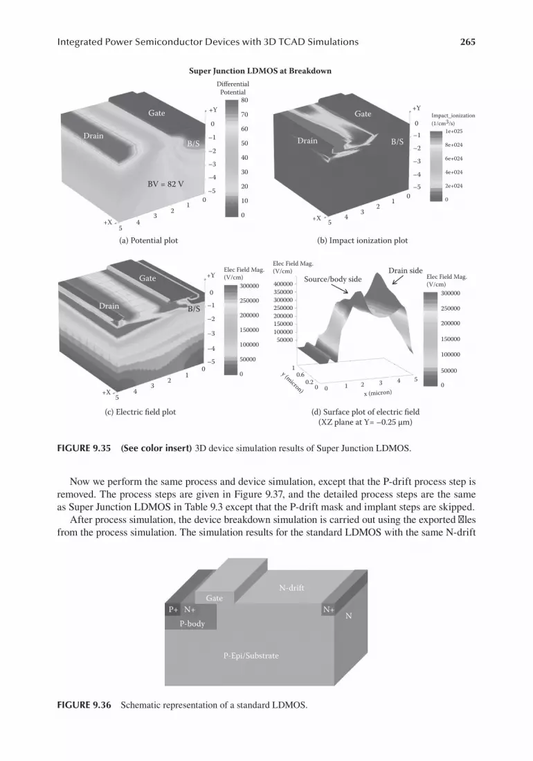
265Integrated Power Semiconductor Devices with 3D TCAD Simulations
Now we perform the same process and device simulation, except that the P-drift process step is removed. The process steps are given in Figure 9.37, and the detailed process steps are the same as Super Junction LDMOS in Table 9.3 except that the P-drift mask and implant steps are skipped.
After process simulation, the device breakdown simulation is carried out using the exported files from the process simulation. The simulation results for the standard LDMOS with the same N-drift
(d) Surface plot of electric field(XZ plane at Y= –0.25 µm)
(c) Electric field plot
(a) Potential plot
Gate
GateGate
Drain
DrainDrain
BV = 82 V
B/S
B/SB/S
Super Junction LDMOS at Breakdown
(b) Impact ionization plot
Drain sideSource/body side Elec Field Mag.
(V/cm)300000
1e+0250
–1
–2
–3
–4
–5
5
DifferentialPotential
80
70
60
50
40
30
20
10–5
–4
–3
–2
–1
0
0 43
21
0
+X5
43
21
0
+X
Impact_ionization(1/cm3/s)
8e+024
6e+024
4e+024
2e+024
0
250000
200000
150000
100000
50000
250000200000150000100000
50000
300000350000400000
Elec Field Mag.(V/cm)
0
Elec Field Mag.(V/cm)
300000
2500000
+Y
+Y+Y
–1
–2
–3
–4
–5
200000
150000
100000
50000
00
12
34
5+X
2 3 4 5100
10.6
0.2
x (micron)
y (micron)
FIGURE 9.35 (See color insert) 3D device simulation results of Super Junction LDMOS.
P-Epi/Substrate
P-bodyN+ N+
N
GateN-drift
P+
FIGURE 9.36 Schematic representation of a standard LDMOS.

266 Integrated Power Devices and TCAD Simulation
doping are shown in Figure 9.38. We show in Figure 9.38a that the breakdown voltage has dropped from 82 to 26 V. Figures 9.38b and c are impact ionization and electric field plots. From the 3D surface plot of electric field of Figure 9.38d, only one electric field peak is observed. This peak is close to the source/body side, which suggests the doping concentration in the N-drift region is too high.
9.3.6 3d simulAtion oF A stAndArd ldmos witH reduced n-driFt doping
To make a fair comparison between the two structures, we deliberately reduce the N-drift doping concentration by modifying the N-drift process step so that the breakdown voltage is on par with the Super Junction LDMOS. The process step that has been modified is shown in Table 9.4.
GateN-plusSpacerP-plus
P-epi N-drift P-bodyP-drift
FIGURE 9.37 Simplified process steps of 3D TCAD simulation of a standard LDMOS.
(d) Surface plot of electric field(XZ plane at Y = –0.25 µm)
(c) Electric field plot
(a) Potential plot
Gate
GateGate
Drain
DrainDrain
BV = 26 V
B/S
B/SB/S
Standard LDMOS at Breakdown
(b) Impact ionization plot
Drain side
Source/body side
Elec Field Mag.(V/cm)
300000
1e+0220
–1
–2
–3
–4
–5
5
DifferentialPotential
25.9027
25
20
15
10
5
0–5
–4
–3
–2
–1
0
–3.81069e-0114
32
10
+X5
43
21
0
+X
Impact_ionization(1/cm3/s)
8e+021
6e+021
4e+021
2e+021
0
250000200000
150000
10000050000
250000200000150000100000
50000
300000350000400000450000
Elec Field Mag.(V/cm)
0
Elec Field Mag.(V/cm)
300000
250000
0
+Y
+Y+Y
–1
–2
–3
–4
–5
200000
150000
100000
50000
00
12
34
5+X2 3 4 5
100
1
0.60.8
0.20.4
x (micron)
y (micron)
FIGURE 9.38 3D device simulation results of standard LDMOS.

267Integrated Power Semiconductor Devices with 3D TCAD Simulations
Figure 9.39 illustrates the device breakdown simulation results after modifications. The break-down voltage is now at 80 V (Figure 9.39a), slightly lower than the Super Junction device of 82 V (Figures 9.39b and c are impact ionization and electric field plots). If we take a look at the electric field surface plot (Figure 9.39d) of the XZ plane at the same location (Y = –0.25 µm), we will see that the electric field distribution is much improved compared with the standard LDMOS (Figure 9.38) with an unmodified N-well by introducing another peak near the drain end.
9.3.7 compArison oF super Junction ldmos And stAndArd ldmos
The LDMOS with a modified N-drift doping condition is compared with the Super Junction LDMOS in terms of breakdown voltage and on-resistance in Figure 9.40. The Super Junction LDMOS is clearly superior in terms of breakdown voltage and on-resistance.
TABLE 9.4Modified Process Step of 3D TCAD Simulation of a Standard LDMOS
Process Step Description3. N-drift implant implant dose = 1e11 energy = 150 phosphorus
implant dose = 3e11 energy = 400 phosphorus
(d) Surface plot of electric field(XZ plane at Y = –0.25 µm)
(c) Electric field plot
(a) Potential plot
Gate
GateGate
Drain
DrainDrain
BV = 80 V
B/S
B/SB/S
Standard LDMOS with Modified N-Drift at Breakdown
(b) Impact ionization plot
Drain side
Source/body side
Elec Field Mag.(V/cm)
300000
1e+0220–1
–2
–3
–4
–5
5
Potential (volt)80.174980706050403020100–1.01203
–5
–4
–3
–2
–1
0
43
21
0
+X54
32
10
+X
Impact_ionization(1/cm3/s)
8e+021
6e+021
4e+021
2e+021
0
25000020000015000010000050000
200000
100000
300000
400000
500000
Elec Field Mag.(V/cm)
0
Elec Field Mag.(V/cm)
300000
250000
0+Y
+Y
+Y
–1
–2
–3
–4
–5
200000
150000
100000
50000
001
23
45+X 2 3 4
5
100
1
0.60.8
0.20.4
x (micron)
y (micron)
FIGURE 9.39 3D device simulation results of standard LDMOS with modified N-drift.

268 Integrated Power Devices and TCAD Simulation
9.4 SUPER JUNCTION POWER FinFET
For low-voltage applications (BV < 100 V), conventional Super Junction structure is not very attractive because the channel resistance is comparable to the drift region resistance. To improve the channel resistance, one novel idea is to make use of the popular FinFET structure [198].
As we know, the FinFET structure has been widely accepted in today’s deep submicron CMOS technologies, partly because the 3D surrounding gate increases the total channel width and effectively reduces the channel resistance. A group of researchers from the University of Toronto and Hong Kong University of Science and Technology have recently demonstrated the interesting idea of integrating a FinFET structure to the Super Junction LDMOS and have successfully reduced the total on-resistance by 30% compared with the conventional Super Junction LDMOS [198].
The basic idea of FinFET + LDMOS is illustrated in Figure 9.41. A 3D corrugated trench MOS gate on the sidewalls and the top surface is used to increase the total channel width (i.e., Wtop + Wside) and to provide a more effective conduction path to the drift region. The deep trench source/drain contact regions also offer a more uniform current flow [198]. A more detailed device structure is given in Figure 9.42.
SOI substrateSOI substrate
Source
Gate
Drain Fill trench with P-pillarto form SJ device
Z YX
n-driftregion
FIGURE 9.41 Basic idea schematics of Super Junction FinFET. (From Abraham Yoo, Jacky C. W. Ng, Johnny K. O. Sin, and Wai Tung Ng, University of Toronto and Hong Kong University of Science and Technology. With permission.)
0.100.090.080.070.060.05Drain Voltage (V)Drain Voltage (V)
(b) On-resistance comparison(a) Breakdown voltage comparison
0.040.030.020.010.0001E–12
1E–11
1E–10
1E–9
1E–8
I-V Curve for Breakdown Voltage (Vg = Vs = 0)
5 10 15 20 25 30 35 40 45 50 55 60 65 70 75 80 850.000000
0.000001
0.000002
0.000003
Dra
in C
urre
nt (A
)
Dra
in C
urre
nt (l
og) (
A)
0.000004
Super Junction LDMOSStandard LDMOS with modifieddrift doping
Super Junction LDMOS
Breakdown and On-Resistance Comparison
LDMOS with modified N-drift doping
On-resistance Simulation (Vg = 5 V)
0.000005
0.000006
FIGURE 9.40 Comparison of breakdown voltage and on-resistance between Super Junction LDMOS and standard LDMOS with modified N-drift doping concentration.

269Integrated Power Semiconductor Devices with 3D TCAD Simulations
9.4.1 process Flow oF tHe super Junction power FinFet
The device is fabricated on a silicon on insulator (SOI) substrate with CMOS compatible technol-ogy. Nine masks are used in fabricating this device. The starting wafer has an N-epi layer on BOX (Buried OXide). A deep trench is etched first to expose the sidewall for the P-body implant. The P-body is formed by ion implantation of the sidewall with an implant tilt of 45 degrees (Figure 9.43a). A deep trench isolation (DTI) process is then carried out to form a thick layer of oxide followed by active lithography and nitride hard-mask etching to define the device active area. The sidewall
Detailed Device Structure and Cross-Sectional Views
(a) Detailed device structure view (b) Cross-sectional views
SJ unit-cellp-substrate
BOXSJ u
nit-cell
SJ unit-cell SJ unit-cell SJ unit-cell
BOX
0.0350.50.5
2.5
0.3 0.30.30.30.30.30.6
Drain
WnWp
(Sn)
Wside
WsideWtop
Wn
Wtop
Wp2.Wn
Wtop
(Sp)TGox
BOX
1.0
2.5
Poly-Si
n-drift
p-drift
DTI
p-body
Cross-section: A-A´B´A´
C´
B
GateZ
Y
X
Source
A
n+n+
n+
C
p+
n+n
p
pDTI
n
Wside Ldrift
Tepip-body
Lch
Cross-section: B-B´
FIGURE 9.42 A more detailed view of the device structure with cross sections. (From Abraham Yoo, Jacky C. W. Ng, Johnny K. O. Sin, and Wai Tung Ng, University of Toronto and Hong Kong University of Science and Technology. With permission.)
(h) Metallization(g) P+ contact opening(f ) N+ source implant(e) N-doped poly gate
(a) P-body implant
P/R
P/RDTIGoxp-
p-body p-body
p-sub p-sub p-sub p-sub
AlSource
Drain
Gate
Poly-Gate
DTI BOX BOX
n-n- n-
P/R
θn–
BOX
Si3N4
p-sub p-sub p-sub p-sub
p-body
p-body p-body
n-n- p-
pp- n-
n- n-
n+ n+
n+n+
p+
n-
p-body p-bodyDTI
P/R
DTI
BOX
BOX
pDTI
θ2
θ
θ1
BOX
BOX BOXLTO
DTI
(b) SJ-drift trench and implant
Breakdown and On-Resistance Comparison
(c) P-pillar diffusion (d) Gate trench
FIGURE 9.43 Simplified process steps for Super Junction FinFET. (From Abraham Yoo, Jacky C. W. Ng, Johnny K. O. Sin, and Wai Tung Ng, University of Toronto and Hong Kong University of Science and Technology. With permission.)
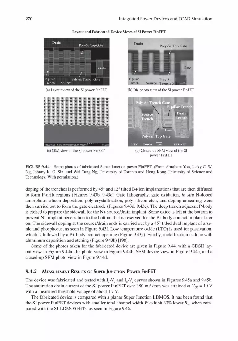
270 Integrated Power Devices and TCAD Simulation
doping of the trenches is performed by 45° and 12° tilted B+ ion implantations that are then diffused to form P-drift regions (Figures 9.43b, 9.43c). Gate lithography, gate oxidation, in situ N-doped amorphous silicon deposition, poly-crystallization, poly-silicon etch, and doping annealing were then carried out to form the gate electrode (Figures 9.43d, 9.43e). The deep trench adjacent P-body is etched to prepare the sidewall for the N+ source/drain implant. Some oxide is left at the bottom to prevent N+ implant penetration to the bottom that is reserved for the P+ body contact implant later on. The sidewall doping at the source/drain ends is carried out by a 45° titled dual implant of arse-nic and phosphorus, as seen in Figure 9.43f. Low temperature oxide (LTO) is used for passivation, which is followed by a P+ body contact opening (Figure 9.43g). Finally, metallization is done with aluminum deposition and etching (Figure 9.43h) [198].
Some of the photos taken for the fabricated device are given in Figure 9.44, with a GDSII lay-out view in Figure 9.44a, die photo view in Figure 9.44b, SEM device view in Figure 9.44c, and a closed-up SEM photo view in Figure 9.44d.
9.4.2 meAsurement results oF super Junction power FinFet
The device was fabricated and tested with Id-Vd and Id-Vg curves shown in Figures 9.45a and 9.45b. The saturation drain current of the SJ power FinFET over 380 mA/mm was attained at VGS = 10 V with a measured threshold voltage of about 1.7 V.
The fabricated device is compared with a planar Super Junction LDMOS. It has been found that the SJ power FinFET devices with smaller total channel width W exhibit 33% lower Ron when com-pared with the SJ-LDMOSFETs, as seen in Figure 9.46.
(c) SEM view of the SJ power FinFET (d) Closed up SEM view of the SJpower FinFET
(b) Die photo view of the SJ power FinFET(a) Layout view of the SJ power FinFET
P-pillarTrench
P-pillarTrench
Poly-Si: Trench Gate Poly-Si:Trench Gate
Poly-Si: Top Gate
20kV X6,000 2 µm UST-NFF
Ldrift
DrainTrench
P-pillar Trench
SourceTrench
Poly-Si: Trench Gate
Poly-Si: Top Gate Poly-Si: Top Gate
Source Source
Drain Drain
Gate Gate
Layout and Fabricated Device Views of SJ Power FinFET
FIGURE 9.44 Some photos of fabricated Super Junction power FinFET. (From Abraham Yoo, Jacky C. W. Ng, Johnny K. O. Sin, and Wai Tung Ng, University of Toronto and Hong Kong University of Science and Technology. With permission.)
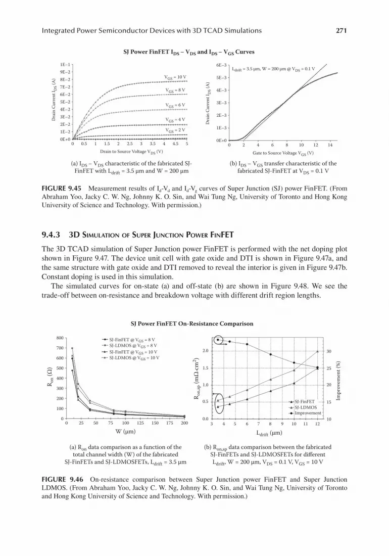
271Integrated Power Semiconductor Devices with 3D TCAD Simulations
9.4.3 3d simulAtion oF super Junction power FinFet
The 3D TCAD simulation of Super Junction power FinFET is performed with the net doping plot shown in Figure 9.47. The device unit cell with gate oxide and DTI is shown in Figure 9.47a, and the same structure with gate oxide and DTI removed to reveal the interior is given in Figure 9.47b. Constant doping is used in this simulation.
The simulated curves for on-state (a) and off-state (b) are shown in Figure 9.48. We see the trade-off between on-resistance and breakdown voltage with different drift region lengths.
(a) IDS – VDS characteristic of the fabricated SJ-FinFET with Ldrift = 3.5 µm and W = 200 µm
SJ Power FinFET IDS – VDS and IDS – VGS Curves
(b) IDS – VGS transfer characteristic of thefabricated SJ-FinFET at VDS = 0.1 V
5 00E+0
1E–3
2E–3
3E–3
4E–3
5E–3
6E–3
2 4 6
Ldrift = 3.5 µm, W = 200 µm @ VDS = 0.1 V
8 10 12 144.53.52.5Drain to Source Voltage VDS (V) Gate to Source Voltage VGS (V)
Dra
in C
urre
nt I D
S (A
)
VGS = 10 V
VGS = 8 V
VGS = 6 V
VGS = 4 V
VGS = 2 V
Dra
in C
urre
nt I D
S (A
)
1.50.500E+01E–22E–23E–24E–25E–26E–27E–28E–29E–21E–1
1 2 3 4
FIGURE 9.45 Measurement results of Id-Vd and Id-Vg curves of Super Junction (SJ) power FinFET. (From Abraham Yoo, Jacky C. W. Ng, Johnny K. O. Sin, and Wai Tung Ng, University of Toronto and Hong Kong University of Science and Technology. With permission.)
(b) Ron,sp data comparison between the fabricatedSJ-FinFETs and SJ-LDMOSFETs for differentLdrift, W = 200 µm, VDS = 0.1 V, VGS = 10 V
SJ Power FinFET On-Resistance Comparison
(a) Ron data comparison as a function of thetotal channel width (W) of the fabricated
SJ-FinFETs and SJ-LDMOSFETs, Ldrift = 3.5 µm
R on (
Ω)
R on,
sp (m
Ω. cm
2 )
W (µm)200
0.03 4 5 6 7 8 9 10 11 12
SJ-FinFETSJ-LDMOSImprovement
Ldrift (µm)
10
Impr
ovem
ent (
%)
15
20
25
30
0.5
1.0
1.5
2.0
175150125100
SJ-FinFET @ VGS = 8 VSJ-LDMOS @ VGS = 8 VSJ-FinFET @ VGS = 10 VSJ-LDMOS @ VGS = 10 V
75502500
100
200
300
400
500
600
700
800
FIGURE 9.46 On-resistance comparison between Super Junction power FinFET and Super Junction LDMOS. (From Abraham Yoo, Jacky C. W. Ng, Johnny K. O. Sin, and Wai Tung Ng, University of Toronto and Hong Kong University of Science and Technology. With permission.)

272 Integrated Power Devices and TCAD Simulation
From Figure 9.49a, we see the simulated impact of gate sidewall width and drain-drift region length on the breakdown voltage. This kind of information is normally not easy to obtain from experiments since a lot of design variations need to be performed and one cannot always tell whether the difference comes from fabrication or real device physics. A benchmark comparison among published data for SJ-LDMOS and SJ power FinFET is shown in Figure 9.49b: the SJ power FinFET is approaching or exceeding the silicon limit.
More simulation results are given in Figure 9.50. On-resistance with respect to distance (a) and electric field with respect to distance (b) are plotted. One of the important merits of TCAD simu-lation is that it can give the engineers an idea of the important physics inside the device, such as electric field distribution, which are difficult to access using pure measurements.
Drain to Source Voltage (V)Drain to Source Voltage (V)
Breakdown and On-Resistance Comparison
On-state @ VG = 10 V Off-state @ VG = 0 V
(b) Simulated off-state curves(a) Simulated on-state curves
2001501005001E–9
I ds (
A)
I ds (
A/c
m2 )
1E–8
1E–7
3 µm
3 µm 3.
5 µm 4
µm4.
5 µm
5 µm
6 µm
8 µm
12 µ
m
3.5 µm
4.5 µm4 µm
5 µm
6 µm 8 µm12 µm
1E–6
1E–5
1E–4400
300
200
100
0 0.02 0.04 0.06 0.08 0.10
FIGURE 9.48 Simulated on-state (a) and off-state (b) curves. (From Abraham Yoo, Jacky C. W. Ng, Johnny K. O. Sin, and Wai Tung Ng, University of Toronto and Hong Kong University of Science and Technology. With permission.)
(b) Net doping plot of the 3D Super JunctionFinFET unit cell with gate oxide and DTI removed
(a) Net doping plot of the 3D Super JunctionFinFET unit cell with gate oxide and DTI
GateChannel
3D TCAD Simulation: Net Doping Plots
N-drift
P-drift
N-drift
P-subP-body P-sub
P-body
FIGURE 9.47 3D TCAD simulation results of Super Junction FinFET unit cell. (From Abraham Yoo, Jacky C. W. Ng, Johnny K. O. Sin, and Wai Tung Ng, University of Toronto and Hong Kong University of Science and Technology. With permission.)

273Integrated Power Semiconductor Devices with 3D TCAD Simulations
(b) Benchmark comparison of on-resistancevs. breakdown voltage for various devices
BV(V)
165 V90 V100
(a) Simulated impact of side wall width(Wside) and drain-drift length (Ldrift)
on breakdown voltage
120
100
80
60
40–30 –25 –20
(Nn – Np)/Np (%)
BV (V
)
R on,
sp (m
Ω. cm
2 )
–15 –100.1
1
Other published data
Simulatedconventional SJ
LDMOS
SimulatedSJ-FinFET
αBV1.9–2.0
(O: 2 µm, ∆: 3 µm)Si-limit
10–5 0
Wside/Ldrift = 2 µm/3 µm
Wside/Ldrift = 3 µm/6 µm
Wside/Ldrift = 2 µm/6 µm
Wside/Ldrift = 3 µm/3 µm
Simulation Analysis of SJ Power FinFET Breakdown Voltage
FIGURE 9.49 Simulated impact of sidewall width (Wside) and drain-drift length (Ldrift) on (a) breakdown voltage and (b) benchmark comparison of on-resistance versus breakdown voltage for various devices. (From Abraham Yoo, Jacky C. W. Ng, Johnny K. O. Sin, and Wai Tung Ng, University of Toronto and Hong Kong University of Science and Technology. With permission.)
Distance (µm)
E fiel
d (×1
05 V/cm
)
Wside = 2 µm
Wside = 3 µm
Distance (µm)00
0.1
0.2
0.3
0.4
0.5
0.6
@ LG = 1 µm, Lch = 0.5 µm, Ld = 3 µm Relaxing the E-field Higher BV
Drainn-drift
Gate
GateSourceRsource Rch Rdrift
Gate
Simulation Analysis of SJ Power FinFET On-Resistance and E-field
Rdrain
SJ SOI-LDMOS
SJ-FinFET
1 2 3 4 5 00
0.5
1.5
2.5
3.5
4.54
2
3
1
1 2 3 4 5
(b) Electric field vs. distance(a) Simulation results of on-resistance vs. distance
R on,
sp (m
Ω. cm
2 )
FIGURE 9.50 Simulation results of (a) on-resistance versus distance and (b) electric field versus distance. (From Abraham Yoo, Jacky C. W. Ng, Johnny K. O. Sin, and Wai Tung Ng, University of Toronto and Hong Kong University of Science and Technology. With permission.)

274 Integrated Power Devices and TCAD Simulation
9.5 LARGE INTERCONNECT SIMULATION
For power devices, the device size is usually fairly large to handle high current and high power. Figure 9.51 is an example of an LDMOS layout showing the source/body and drain contacts, gate, and active area (silicon area without STI or DTI). The device cross section is illustrated underneath the layout. The configuration of this layout features a source (S)–drain (D)–drain (D)–source (S) arrangement, which is typical for an LDMOS with extended drain region.
If the LDMOS is required to handle high current, the device width has to be designed large enough to reduce the total on-resistance and, thus, the power dissipation. With larger device sizes, the on-resistance coming from the device itself drops, but unfortunately the total measured resistance does not drop accordingly. This is because with high current levels and large device sizes the voltage drop on the metal interconnects is no longer negligible: the resistance contribution of metal interconnects can be even greater than that from the device itself, a phenomenon frequently referred to as metal debiasing.
TCAD is used to simulate the large interconnect resistance and see the current/temperature dis-tributions. Our goal in this section is to build an interconnect structure with three metal layers that resides on a highly conductive silicon substrate. To make simulation easier, we neglected the active device part and focus only on the interconnect structure. The highly doped silicon substrate is used to eliminate the resistance contribution from the device so that the majority of the resistance comes from the interconnect itself.
Figure 9.52 shows the layout view of contacts that touch the highly doped silicon surface, with a cross-section view. We see a symmetrical (S–D–S–D) configuration with a small voltage (0.1 V) applied to all the drain contacts while keeping source contacts grounded. Current flows in silicon substrate are depicted in the cross-section view of Figure 9.52. The resistance between source and drain is made very small by laying out all the S–D pairs in parallel; the width is large enough to neglect the small resistance from source to drain in the highly doped substrate. In the following sections, we will present a detailed simulation demonstration of a complicated interconnect structure.
P-Epi/P-Sub
Active Area
Active Area Active AreaPoly Gate Poly Gate
DrainContacts
SourceContacts
S
S
S
S
S
S
S
S
S S S
S
S
S
S
S
S
S
S
S
S
S
S
S
S
S
S
S
S
S
S
S
S
S
S
D
D
D
D
D
D
D
D
D
D
D
D
D
D
D
D
D
D
D
D
D
D
D
D
D
D
D
D
D
D
D
D
D D SN DrainSTISTISTI
Gate Gate Gate GateN PNNN PPP N DrainN DrainN Drain
PbodyPbodyPbodyPbody
D D
GatePoly GateGateActive Area
FIGURE 9.51 Layout example of a large LDMOS.

275Integrated Power Semiconductor Devices with 3D TCAD Simulations
9.5.1 3d process simulAtion oF tHe lArge interconnect
The simulation starts with a heavily doped N-type silicon substrate (with phosphorus) to mimic the active device when the gate is fully on. With a doping concentration of 1E + 19 cm-3, the resistance from the substrate is kept at a minimum. A total of three metal layers are simulated with simulation size of 100 µm by 100 µm. The metal layers are arranged so that metal1 corresponds to the stripes, metal2 the buses (wider than metal1), and metal3 the blocks (wider than metal2); a schematic view of the metal scheme is given in Figure 9.53. Metal1 stripes are connected to source or drain by the contacts, and they are patterned in a S–D–S–D configuration. Via1 connects metal1 and metal2, and they are placed so that metal1 for the source is connected to metal2 for the source. Metal2 regions are typically thicker and wider than metal1, but for the purpose of a simulation demonstra-tion the thicknesses of all the metals are set to be 0.5 µm. This, of course, is not the case in real
Via2SS
S
S
S
S D
D
D
D D
Via1
Metal1
Metal2
Metal3
FIGURE 9.53 Metal layout scheme with metal1 in stripes, metal2 in buses, and metal3 in blocks.
Current flow
S D D DS S
S D D DS S
S D D DS S
S D D DS S
S D D DS S
S D D DS S
S D D DS S
S D D DS S
S D D DS S
0 V 0.1 V 0.1 V 0.1 V0 V 0 V
Current flow Current flow
N+ doped (1E+19 cm–3) substrate
FIGURE 9.52 The simplified layout for large interconnect simulation.

276 Integrated Power Devices and TCAD Simulation
manufacturing where metal3 is substantially thicker than metal1 and metal2. From Figure 9.53, we see that metal2 buses are placed horizontally, with S–D–S–D in the vertical direction. Metal3 regions are designed to be in large blocks: two blocks are used in this simulation, with the source on the left and the drain on the right. Metal3 blocks are connected by via2 from metal2.
The simplified process steps are shown in Figure 9.54, whereas the complete layout of the inter-connect structure is illustrated in Figure 9.55. Six mask layers (contact, metal1, via1, metal2, via2, and metal3) are used in this design, and aluminum is used for all layers (including contacts and vias) for the sake of simplicity.
9.5.1.1 SubstrateSince the purpose of this 3D example is to simulate a complicated interconnect, if we use the standard procedure to build an LDMOS or an analog MOS, the simulation will be much more complicated and time-consuming. Instead, we just use an N+ doped silicon substrate with phosphorus concentration of 1E + 19 cm-3 so that only the back-end is simulated. The simulation result is shown in Figure 9.56.
9.5.1.2 ContactsThe ILD1 layer is deposited, and contact holes are etched. Aluminum is used in the simulation to fill those contact holes. After filling, a CMP step is performed to prepare the surface for the metal1 layer.
Contacts
Metal1
Metal2
Metal3
Via2
Via1
FIGURE 9.55 Layout of the large interconnect structure.
Metal3
Metal1ContactsN-sub
Metal2Via2
Via1
FIGURE 9.54 Simplified process steps of 3D TCAD simulation of a complicated interconnect.

277Integrated Power Semiconductor Devices with 3D TCAD Simulations
The height of the contacts is 0.5 µm with a size of 2 µm by 2 µm. There are totally 25 × 25 = 625 contacts in this simulation, as shown in Figure 9.57.
9.5.1.3 Metal1Aluminum metal stripes are used to connect the contacts in the vertical direction. After deposi-tion, aluminum is etched with the metal1 photomask. The thickness of the metal1 layer is 0.5 µm. The metal stripe has a width of 2 µm, length of 100 µm and runs in the z direction, as shown in Figure 9.58. A total of 25 metal1 stripes are simulated. Please note that in real practice design rules may require the dimension of a metal1 width larger than the width of square contacts and via1s.
9.5.1.4 Via1The next step is to place via1 on top of metal1. Since metal1 connects the underlying contacts in S–D–S–D fashion, via1 are used to connect metal1 (source) to metal2 (source) and metal1 (drain) to metal2 (drain). Each via1 row is placed onto the metal1 stripes on either an odd number or even number of the metal1 columns, as shown in Figure 9.59. Like the contacts, oxide is first deposited to create ILD2 before via1 holes are etched and filled. Chemical mechanical polishing is performed to flatten the surface and prepare for the metal2 step.
9.5.1.5 Metal2The process step of metal2 is similar to metal1, with a thickness of 0.5 µm. Metal2 lines are drawn in wider buses and are placed in a horizontal direction as shown in Figure 9.60. 10 metal2 buses are simulated, each with a width of 8 µm and a length of 100 µm.
100+Z
8060
4020
0020406080100
+X
Net_Doping19
FIGURE 9.56 Substrate net doping plot.
Metal3 40 20 0 020
4060
80100
+Z
6080100
SiO2AlSi
+X
Material Number
(b) Simulation result after contacts etch, fill, and polish(a) Mask layout of contacts
Metal2
Metal1
Contacts
Via2
Via1
FIGURE 9.57 3D process simulation of large interconnect: (a) Mask; (b) After contacts CMP.

278 Integrated Power Devices and TCAD Simulation
Metal3 40 20 0 020
4060
80100
+Z
6080100
SiO2AlSi
+X
Material Number
(b) Simulation result after metal2 deposit and etch(a) Mask layout of contacts + metal1 + via1 + metal2
Metal2
Metal1
Contacts
Via2
Via1
FIGURE 9.60 3D process simulation of large interconnect: (a) Mask; (b) After metal2 step.
Metal340 20 0 0
2040
6080
100
+Z
6080100
SiO2AlSi
+X
Material Number
(b) Simulation result after metal1 deposit and etch(a) Mask layout of contact + metal1
Metal2
Metal1
Contacts
Via2
Via1
FIGURE 9.58 3D process simulation of large interconnect: (a) Mask; (b) After metal1 etch.
Metal340 20 0 0
2040
6080
100
+Z
6080100
SiO2AlSi
+X
Material Number
(b) Simulation result after via1 etch, fill and polish(a) Mask layout of contact + metal1 + via1
Metal2
Metal1
Contacts
Via2
Via1
FIGURE 9.59 3D process simulation of large interconnect: (a) Mask; (b) After via1 step.

279Integrated Power Semiconductor Devices with 3D TCAD Simulations
9.5.1.6 Via2Via2 are placed on top of metal2 to connect metal2 and metal3. Like via1 and contacts, each via2 region is a 2 µm by 2 µm square. They are placed so that metal2 buses for the source are connected to the metal3 block for the source, and metal2 buses for drain are connected to the metal3 block for the drain, as shown in Figure 9.61.
9.5.1.7 Metal3The final step is to deposit and etch metal3. Two metal3 blocks are drawn for the source and drain, respectively. Each metal3 block is 48 µm wide and 100 µm long, as shown in Figure 9.62. The oxide ILDs are deliberately removed to show the inside.
Metal3 40 20 0 020
4060
80100
+Z
6080
100
SiO2AlSi
+X
Material Number
(b) Simulation result after via2 etch, fill, and polish(a) Mask layout of contacts + metal1 + via1 +metal2 + via2
Metal2
Metal1
Contacts
Via2
Via1
FIGURE 9.61 3D process simulation of large interconnect: (a) Mask; (b) After via2 step.
Metal3 40 20 0 020
4060
80100
+Z
6080100
AlSi
+X
Material Number
(b) Simulation result after metal3 deposition and etch(a) Mask layout of contacts + metal1 + via1 +metal2 + via2 + metal3
Metal2
Metal1
Contacts
Via2
Via1
FIGURE 9.62 3D process simulation of large interconnect: (a) Mask; (b) After metal3 step.

280 Integrated Power Devices and TCAD Simulation
9.5.2 3d device simulAtion oF tHe lArge interconnect
Before we can do device simulation, we need to place contacts (i.e., equipotential boundary conditions) on the metal3 blocks. In this simulation, the contacts have a square shape with a size of 10 µm by 10 µm. Since the metal3 blocks are very large, the location of contacts will influence the device simulation result. We arbitrarily placed the contacts at the locations shown in Figure 9.63a. A small voltage bias of 0.1 V is applied to the drain (right contact on the metal3 block) with the self-heating model turned on. We can view the differential potential, total current magnitude, and lattice temperature plots in Figure 9.63b–d. The thermal boundary for the contacts consists of a heat sink with a constant temperature of 300 K connected via a thermal conductance of 100 W/K.
(d) Lattice temperature plot
(b) Differential potential plot
Simulation Results of the Large Interconnect
(c) Total current magnitude plot
(a) Contacts placement
100–X
FEM_StructureAl(xlam–0.55)Si
80 60 40 20 0 020
4060
80100
0.1
0.08
0.06
0.04
0.02 100 80 60 40 20 0 020
4080
100
10080
6040
200020406080100100
5e+0064.5e+0064e+0063.5e+0063e+0062.5e+0062e+0061.5e+0061e+0065000000
80 60 40 20 0 020
4060
80100
–Z
–X –X
–Z
480460440420400380360340320300
60
0
–X
–Z–Z
Differential Potential
Lattice Temperature (K)Total Curr. Mag (A/cm2)
FIGURE 9.63 (See color insert) 3D device simulation results of the large interconnect with (a) contacts placement, (b) differential potential, (c) total current magnitude, and (d) lattice temperature.

281
10 GaN Devices, an Introduction
Strictly speaking, GaN power devices are not considered integrated power devices even though high electron mobility transistors (HEMTs) have a lateral current flow path similar to that of LDMOS. However, researchers [199] [200] have already started exploring the possibility of using gallium nitride (GaN) for smart power IC. It is therefore useful to give readers an introduction to this topic, especially since many people in the field are familiar only with silicon.
10.1 COMPOUND MATERIALS VERSUS SILICON
Silicon has been the dominant material for power semiconductor devices for many years. Given the economies of scale due to existing infrastructure, mature technology, and innovative structures and devices like RESURF, Super Junction, and IGBT, silicon devices are still predicted to be the domi-nant material in the foreseeable future. However, ever-increasing demands for higher efficiency and better performance are beginning to approach the silicon limit, and this technology is expected to saturate in a few years’ time. Recently, compound materials such as 4H silicon carbine (4H-SiC) and GaN are drawing the attention of semiconductor companies. In fact, if we define figures of merits (FOMs) such as Rdson, Rdson x QSW or efficiency × density/cost [201], as shown in Figure 10.1 we see that as silicon-based power device technology reaches maturation GaN-based power devices appear ready to continue to provide the rapid and dramatic improvement in performance that the electron-ics industry enjoyed over the past 30 years.
A comparison is made between silicon, 4H-SiC, and GaN [202] [203] in Table 10.1. Both 4H-SiC and GaN have large bandgaps and can support a 10x higher critical electric field. SiC also has a better thermal conductivity, which makes thermal design of power devices more convenient. Unfortunately, SiC is too expensive a material for most power electronics system providers. As we mentioned earlier, power electronics and especially power supplies are very price-sensitive. On the other hand, GaN is less expensive, since there is already an installed base for high-brightness light-emitting diode (HB LED) applications.
The higher FOMs in Table 10.1 indicate the capability of these materials of operating at higher switching frequencies and at higher voltages with faster reverse recovery [203]. GaN also benefits from a particularity of its crystal structure (polarization), which can be harnessed to create a 2DEG (2-Dimensional Electron Gas); this will be discussed later in this chapter. The remainder of this chapter focuses solely on GaN devices; interested readers can refer to books such as [158] for a detailed analysis of SiC power devices.
This chapter gives the reader a step-by-step introduction to GaN devices by TCAD simula-tion. Starting from a single layer of GaN, we will explore the unique characteristics of the device that are associated with the polarization effect. This is followed by a stack of AlGaN layers to examine the band diagram around the 2DEG channel. A gate contact is then introduced to see how the 2DEG channel is pinched off by applying a gate potential. Finally, the source and drain are added to make a complete HEMT device. More complicated devices are introduced at the end of this chapter.

282 Integrated Power Devices and TCAD Simulation
10.2 SUBSTRATE MATERIALS FOR GaN DEVICES
GaN devices can be grown on various substrates. The most commonly used substrates include silicon, silicon carbine (SiC), and GaN. It has been found that, in terms of defect density, lattice mismatch, reliability and yield, as well as off-state leakage, GaN substrate outperforms Si or SiC counterparts [204], [205], as listed in Table 10.2. (The Al2O3 substrate is omitted here due to very low thermal conductivity and a relatively high cost that limits its usefulness for power applications.)
Unfortunately, a relatively modest 2-inch GaN substrate can cost as much as $1900 in 2012 [206], compared with as little as $25 for a 6-inch silicon wafer. Since power electronics and power management systems are often cost-sensitive, the reasons for the push toward GaN-on-silicon are obvious. Besides much lower wafer cost, GaN-on-silicon can also leverage existing infrastruc-ture, despite the fact that it has a large lattice mismatch and difference in thermal expansion coef-ficients. In the meantime, it is expected that cheaper GaN and SiC wafers will become available as the technology matures. This chapter focuses on simulations of GaN devices with Si or SiC substrates.
TABLE 10.1Material Property Comparison between Silicon, 4H-SiC and GaN
Material Property Silicon 4H-SiC GaN
Bandgap (eV) 1.1 3.2 3.4
Critical field (1E+6V/cm) 0.3 3 3.5
Electron mobility (cm2/V-Sec.) 1450 900 2000
Electron saturation velocity (1E+6 cm/Sec.)
10 22 25
Thermal conductivity (W/cm2K) 1.5 5 1.3
Baliga FOM = ε µEs c3 1 675 3000
TABLE 10.2GaN Device Properties on Different Substrates [204] [205]
Attributes Si Substrate SiC Substrate GaN Substrate
Defect density (cm–2) 1E+9 5E+8 1E+3 to 1E+5
Lattice mismatch (%) 17 3.5 0
Thermal conductivity (W/cm-k at 25 °C) 1.5 3.0~3.8 1.5
Coefficients of thermal expansions (%) 54 25 0
Breakdown voltage (V) 200 600 1700
Off-state leakage High High Low
Reliability and yield Low Low High
Lateral or vertical device Lateral Lateral Lateral or vertical
Integration possibility Very high Moderate —
Substrate size (mm) (as of 2012) 400 150 50
Substrate cost (relative) Low Very high Very high

283GaN Devices, an Introduction
10.3 POLARIZATION PROPERTIES OF III-NITRIDE WURTZITE
10.3.1 microscopic dipoles And polArizAtion vector
It is well-known that III-Nitride materials (GaN, InN, AlN, and their alloys) exhibit polarization charge behavior that must be accounted for in designing GaN power devices. Without getting into theoretical details, we use a simplistic view to explain the origin and underlying physics of polariza-tion in this section.
By polarization behavior, we mean that microscopic dipoles form within the bulk of the material (see Figure 10.2a). A microscopic dipole can be denoted by the charge (e) and the separation between the negative and positive charges (d):
ed (unit m-Coulomb). If the density
of dipoles is defined as ρd , we can express the quantity of interest as the polarization vector p :
= ρp edd (10.1)
where the polarization is given in units of Coulomb/m2.
2009 Year
Silicon Maturation
Next Gen Si
Super Junction
TrenchFET
HEXFETVFETBipolar
FOM
GaN HEMT
20031978
Si
GaN
Figu
re o
f Mer
it (F
OM
)
FIGURE 10.1 Trend of FOM for silicon and GaN devices over the years.
(b) Schematic diagram indicatingsurface charge reduction by rough
surfaces
(a) Schematics showing how macroscopicsurface charge layers are formed by bulk
polarization or microscopic dipoles
Positive Surface Charge
Negative Surface Charge
Microscopic dipole
ed
+
–
Reduced Negative Surface Charge
Reduced Positive Surface Charge
FIGURE 10.2 (a) Schematics showing how macroscopic surface charge layers are formed by bulk polariza-tion or microscopic dipoles; (b) Schematic diagram indicating surface charge reduction by rough surfaces.

284 Integrated Power Devices and TCAD Simulation
In an infinite homogeneous nitride material with uniform polarization density, the positive and negative charges of the dipoles would cancel each other within the bulk, and net charges appear only on a flat surface that is perpendicular to the vector of the polarization (pointing from the negative charge to the positive charge) dipole vector (see Figure 10.2a). Please note that net surface charges do not appear on surfaces that are parallel to the dipole vector, and the amount of charges would be reduced if the surface makes an angle with the dipole vector. In a rough surface or rough interface, nonflat regions would form angles with the dipole vector; thus, the net surface charges would be reduced compared with a flat surface or interface (see Figure 10.2b). Such a geometric charge reduc-tion effect explains why surface and interface quality affects the amount of net surface charges.
10.3.2 crystAl structure And polArizAtion
Similar to how silicon atoms connect to four neighbors in a lattice, in GaN each Ga atom connects to four N-atoms; alloys in the III-nitride family are the same with In or Al substituting for Ga. However, unlike the diamond cubic configuration found in silicon, the most common and stable crystal con-figuration for III-nitrides is a hexagonal close packed (hcp) Wurtzite structure (Figure 10.3).
We note that N has a high electronegativity (3.04) compared with Ga (1.81), so the GaN bonds are strongly ionic. This means that the hexagonal crystal structure is responsible for the microscopic polar-ization observed in GaN: if the dipoles do not cancel each other out because of how the atoms are placed in the lattice, then a net polarization vector forms in the direction in which the atoms stack (c-axis).
Two arrangements are possible depending on how the bonds are aligned with respect to the substrate surface. By convention, the Ga-to-N bond along the c-axis is defined as the [0001] direction, and substrates with this bond on the outer surface are called Ga-face. Substrates grown in the other direction [0001] are called N-face and exhibit a polarization vector direction opposite to that of Ga-face substrates.
The formation of Ga-face or N-face structures is almost entirely the result of the process and growth conditions; if one is not careful, different N-face and Ga-face regions can even form on the same substrate (domain reversal). In general, MOCVD processes tend to produce Ga-faced substrates, whereas N-faced substrates are favored in MBE. With the technology currently avail-able, Ga-face crystals also tend to be of a higher quality and are cheaper and faster to grow. Since MOCVD is also the favored growth method for the industry, Ga-faced crystals are commonly used, and we will therefore limit ourselves to this configuration.
10.3.3 ideAl c0/a0 rAtio For zero net polArizAtion
Close examination of the structure in Figure 10.3 indicates that the GaN microscopic dipoles vector projected along the c-axis have different signs and tend to cancel each other. Defining the lattice
SubstrateSubstrate
Ga-face N-face
Ga
GaN
N
[000
1]
[000
1]_
FIGURE 10.3 Atomic arrangement in Ga-face (a) and N-face (b) GaN crystals. The arrows show the direc-tion of microscopic dipoles.

285GaN Devices, an Introduction
constant of Wurtzite in the stacking direction as c and in the hexagonal plane as a, we will show that for a specific c/a ratio the net dipole will be zero and the crystal will have no net polarization. A zero subscript is added to the lattice constant of a relaxed and bulk material since strained lattice constants are often used.
Projecting the microscopic dipoles along the c-axis is the same as projecting the bond length (d) onto the c-axis (dz). The dipoles will therefore cancel each other out if
=d dz3 (10.2)
Examining the structure, we find the lattice constants can be defined using the bond length and its projections:
= +c d dz2 2 (10.3)
=a dx2 (10.4)
Some basic vector analysis using the previous equations leads to the ideal c/a ratio for zero polarization:
= =c
a
83
1.6330 (10.5)
Since all of the III-N compounds (Ga-faced) have c a/0 0 ratios (1.6010 for AlN; 1.6259 for GaN; 1.6116 for InN) smaller than the aforementioned ideal ratio, the three Ga-N bonds have shorter dz and thus all exhibit a negative spontaneous polarization with the polarization vector pointing toward the substrate. This kind of polarization due to crystal asymmetry is termed spontaneous polarization.
10.3.3.1 Strain-Induced PolarizationIf the c0/a0 ratio of the III-N lattice is forced to deviate from the above ideal ratio of 8/3, the polariza-tion of the crystal is affected. One way to change the c0/a0 ratio is through strain, such as in pseudo-morphic epitaxial growth on a different III-N material. During pseudomorphic epitaxy, the material expands or contracts to match the in-plane lattice constants of the underlying layer. When in-plane lat-tice constant a changes in one way, the c must change in the other way to preserve the total bulk volume.
As a result of the in-plane lattice constant change, the c0/a0 ratio changes, which in turn changes the polarization strength. The additional polarization in strained III-N layers is termed piezoelectric polarization.
Let us consider the case of InGaN and AlGaN growing on GaN and the overall lattice spacing is that of the GaN substrate. The lattice constants (a0) are 3.189, 3.544, and 3.111 Å for GaN, InN, and AlN, respectively. Therefore, InGaN would experience biaxial compressive strain in the plane parallel to the substrate and the c0/a0 ratio would be increased toward the ideal ratio, which in turn reduces the polarization strength. In another word, the sign of piezoelectric polarization for InGaN is positive.
On the other hand, AlGaN would experience biaxial tensile strain in the plane parallel to the sub-strate and the c0/a0 ratio would be reduced from the ideal ratio, which in turn increases the polarization strength. In other words, the sign of piezoelectric polarization for AlGaN is negative. Please note that AlGaN enhancing the polarization charges is especially significant since a strong polarization induces the triangle quantum well for formation of 2D electron gas in a power GaN HEMT structure.
We therefore note the importance for TCAD modeling of GaN devices to know the reference lattice of the crystal and any external stress terms to properly calculate the strain and polarization in the device. This is especially challenging for GaN-on-silicon where the difference in thermal expansion coefficients leads to external stress or cracks when the structure cools down to room

286 Integrated Power Devices and TCAD Simulation
temperature. In practice, one or more thick layers of GaN is usually grown and allowed to relax to ensure that all subsequent epi layers will follow the GaN lattice.
10.3.3.2 Empirical Approach to Modeling PolarizationThe previous subsections use a simplistic explanation to account for the origin of spontaneous and piezoelectric polarizations in III-N materials. A rigorous calculation is rather involved, and a com-mon approach is to express the total polarization as an empirical function of material composition (see, e.g., [207]).
Usually, the polarization is given for binaries of GaN, InN, and AlN and for arbitrary compo-sition; a linear combination is taken with a second-order correction term (bowing). We take one example of AlxGa1−xN from reference [207] here. The spontaneous polarization psp in units of e/m2 can be expressed as
= − − − + −P x x x xsp 0.09 0.034(1 ) 0.019 (1 ) (10.6)
For computation of piezoelectric polarization, we need to calculate the strain ε as
ε = −a a aGaN AlGaN AlGaN( )/0, 0, 0, (10.7)
Then, the piezoelectric polarization Ppz AlN, for AlN can be written as
= − ε + ε ε <P forpz AlN 1.808 5.624 ; ( 0),
2
(10.8)
= − ε − ε ε >P forpz AlN 1.808 7.888 ; ( 0),
2
(10.9)
Similarly, for GaN
= − ε + εPpz GaN 0.918 9.541,2
(10.10)
Piezoelectric polarization for the compound is obtained by linear combination:
= + −P P x P xpz pz AlN pz GaN (1 ), , (10.11)
The total polarization for AlGaN can be finally expressed as
= +P P PAlGaN sp pz (10.12)
Please note that the empirical formula (10.12) is the full amount of polarization charges that can be measured. In real devices, rough surfaces and interface defects may introduce a screening factor, and usually some fraction (say 30 to 70 percent) of the previous full polarization is used in TCAD simulation.
As an example, the polarization is simulated with a TCAD device simulator (APSYS) accord-ing to the formula found in [208] with a screen factor of 0.7 (70 percent); a factor of unity means 100 percent of the theoretical interface charge is used. This screening factor is used to account for deviations from the theory such as screening by charged fixed defects and partial relaxation. As seen Figure 10.4a, polarization charges in the TCAD simulator are represented by fixed charges. The top has negative fixed charges, while the bottom has positive charges. Unlike silicon, which has no polarization effect, a tilted band diagram is obtained if we draw a 1D cutline from top to bottom, as shown in Figure 10.4b. Note that for the moment we ignore the compensation and passivation of charges on the exposed surface that would occur in a real device.

287GaN Devices, an Introduction
10.4 AlGaN/GaN HETEROJUNCTION
By adding an AlGaN layer on top of a GaN layer, we create a heterojunction: the AlxGa(1-x)N/GaN heterojunction is widely used in devices such as HEMTs. Here, x is the mole fraction of aluminum in the AlGaN material. With AlGaN grown on top of GaN, the band diagram near the interface is altered due to the polarization mismatch of the two materials and the resulting interface charges. As an example, the band diagram for x = 0.3 (Al0.3Ga0.7N/GaN) is plotted side by side with x = 1 (AlN/GaN) on Figure 10.5. The AlxGa(1–x)N layer is 30 nm thick in both cases, but only a 10 nm window near the material boundary is shown.
From Figure 10.5, we note the formation of a triangular well in the conduction band at the inter-face. This region is very thin and will serve to confine carriers on a two-dimensional plane (i.e., a quantum well) leading to the formation of a two-dimensional electron gas (2DEG). We note that as the Al fraction in AlGaN increases, the bandgap of AlGaN increases as does the polarization mismatch; as a result, the triangular electron well becomes deeper and deeper. As the bottom of the well dips below the Fermi level, a high carrier sheet density is formed that provides for a large
(b) Band diagram plot of GaN material(cutline from top to bottom)
(a) Simulated GaN material polarization effect
Polarization Charge (positive)
Distance (um)0.002
0.010.0080.0060.0040.00200
0.002
0.004
0.006
0.008
0.01
–3
–2
–1
0
121.421Net_Fix_Charge
20151050
–5–10–15–20–21.421
Ener
gy (e
V)
2
3
0.004 0.006 0.008
Band DiagramE_vE_fE_c
0.01
Polarization Charge (negative)
GaN Material
Single GaN Layer Simulation with Polarization and Band Diagram Plots
FIGURE 10.4 Simulated GaN material polarization effect.
(b) Band diagram plot of AlN/GaN structurewith AlN layer thickness of 30 nm
(a) Band diagram plot of Al0.3 Ga0.7N/GaNstructure with Al0.3 Ga0.7N thickness of 30 nm
Distance (um)
0 0.002–4
–3.5–3
–2.5
–1.5
Ener
gy (e
V)
Ener
gy (e
V)
–0.5
0.50
–1
–1
–2
–3
–4
–5
–6
–7
–8
0
–2
0.004 0.006 0.008 0.01 0 0.002 0.004 0.006 0.008 0.01
Band DiagramE_vE_fE_c
Band DiagramE_vE_fE_c
2DEG Region
2DEG Region
AlN GaNGaN
Distance (um)
Band Diagram Plots of Al0.3 Ga0.7N/GaN and AlN/GaN Structures
Al0.3 Ga0.7N
FIGURE 10.5 Band diagram plots of AlxGa(1–x)N/GaN heterojunction with (a) Al0.3Ga0.7N/GaN and (b) AlN/GaN.

288 Integrated Power Devices and TCAD Simulation
number of carriers in the channel without relying on doping. This means that the channel mobility is increased (with less scattering) and the on-resistance is reduced.
For readers with a silicon background, we can correlate the AlGaN/GaN with SiO2/Silicon in a MOSFET. AlGaN is a material with a much larger (4 eV for 30% Al, 6 eV for AlN) bandgap than GaN (3.4 eV), so it serves the same role as the oxide (which has a much larger bandgap than silicon). It is also known that for N-type MOSFETs under strong inversion a thin layer of highly concentrated electrons appears close to the SiO2/Si interface: this thin layer of electrons analogous to the 2DEG formed in our AlGaN/GaN heterojunction.
The most important difference compared with a silicon MOSFET is that it is not necessary to create a strong inversion or use doping to form a 2DEG in a GaN HEMT; instead, the built-in polarization mismatch at the interface does all of the work and the 2DEG is present even under equilibrium conditions. We therefore need to study the influence of the Al mole fraction x and the thickness of the AlGaN layer on our 2DEG.
10.4.1 BAnd diAgrAm plots witH A Fixed Al mole FrAction
If we arbitrarily select a fixed x value, for example, x = 0.3, we can vary the thickness of the AlxGa(1–x)N layer to see the how the layer thickness affects the 2DEG. In Figure 10.6, simulated band diagrams at equilibrium for Al0.3Ga0.7N layer thicknesses of 15 nm, 20 nm, 35 nm, and 45 nm are plotted. No metal contacts or surface passivation are used in these simulations. We note that
Band Diagram at Equilibrium of GaN-AlGaN Structure with Various AlGaN Layer ickness
(d) Band diagram plot of GaN-AlGaN structurewith Al0.3 Ga0.7N layer thickness of 45 nm
(b) Band diagram plot of GaN-AlGaN structurewith Al0.3 Ga0.7N layer thickness of 20 nm
(c) Band diagram plot of GaN-AlGaN structurewith Al0.3 Ga0.7N layer thickness of 35 nm
(a) Band diagram plot of GaN-AlGaN structurewith Al0.3 Ga0.7N layer thickness of 15 nm
0.01
Band DiagramE_v
E_cE_f
Band DiagramE_v
E_cE_f
Band DiagramE_v
E_cE_f
Band DiagramE_v
E_cE_f
0.0080.006Distance (um)
0 0.002 0.004 0.006 0.008 0.01Distance (um)
Al0.3 Ga0.7N35 nm
Al0.3 Ga0.7N15 nm
Al0.3 Ga0.7N45 nm
Al0.3 Ga0.7N20 nm
0.0040.0020 0.010.0080.006Distance (um)
0.0040.0020
0.010.0080.006Distance (um)
0.0040.0020
–4
–3
–3
–2
–2
–1
–1
Ener
gy (e
V)
Ener
gy (e
V)
Ener
gy (e
V)
Ener
gy (e
V)
0
0
1
2
0
0
1
–0.5
–1.5
–2.5
–3.5–4
–4
–1
–1
–2
–2
–3
–3
FIGURE 10.6 Band diagram plots of Al0.3Ga0.7N/GaN heterojunction with different layer thickness of (a) 15 nm, (b) 20 nm, (c) 35 nm, and (d) 45 nm.

289GaN Devices, an Introduction
the 2DEG region gets larger with a thicker Al0.3Ga0.7N layer thickness; at 15 nm, the triangular well is so shallow that no 2DEG region can be found. The band diagrams give us a clue on how high the electron concentration can be near the interface: thicker AlGaN layers result in a higher sheet charge and thus a lower resistivity during the on-state. This layer thickness-2DEG relation-ship applies to all x values.
This band diagram dependence on the Al0.3Ga0.7N layer thickness can be clarified by superposing the conduction bands in Figure 10.7. Different layer thickness yields different 2DEG sizes, and for any given Al fraction there is a critical thickness below which the 2DEG ceases to exist.
In addition to this minimum thickness, in real manufacturing processes there is also a maximum thickness that can be used. Readers familiar with compound semiconductor growth will surely know about the concept of critical film thickness [209]: beyond this thickness, thin films under stress start to relax and take on their natural bulk lattice constant rather than that of the substrate. In addition to the cracking such relaxation would induce, the 2DEG would also be affected since relaxation reduces strain in the layer and therefore affects the polarization mismatch [210] [211]. According to published data [205], the most commonly used AlGaN layer thicknesses are around 15 nm to 30 nm.
10.4.2 BAnd diAgrAm plots witH A Fixed Algan tHickness
For a fixed AlGaN layer thickness to 30 nm, we can observe the effects of the Al mole fraction in Figure 10.8. For small Al content, the 2DEG is also not found for this thickness, which suggests that a thicker layer would be needed. At larger concentrations, the well is deeper, which leads to a larger 2DEG concentration and lower on-resistance in the channel. A more detailed comparison is also made in Figure 10.9.
Again, real device processes limit what can be accomplished, and it is not always possible to sim-ply use a larger Al fraction. Cracks may appear if the Al mole fraction is too large [211]. According to published data [205], the most commonly used Al mole fractions are from x = 0.15 to x = 0.3.
10.4.3 Algan/gan structure witH doped Algan or gan lAyer.
It has been found that adding dopants in the AlGaN layer can modify the 2DEG sheet charge. For example, for the case of Al0.25Ga0.75N/GaN with an AlGaN layer thickness of 25 nm, a heavier
0.0400.035
Fermi potential at equilibrium
0.0300.0250.020Distance (um)
0.0150.0100.005–1.0
–0.5
0.0
0.5
1.0
2.0
1.5
2.5
3.0
3.5
4.0
4.5
Conduction Band Diagrams of Al0.3Ga0.7N with Various Layer ickness
Al0.3Ga0.7N layer thickness = 50 nmAl0.3Ga0.7N layer thickness = 45 nmAl0.3Ga0.7N layer thickness = 40 nmAl0.3Ga0.7N layer thickness = 35 nmAl0.3Ga0.7N layer thickness = 30 nmAl0.3Ga0.7N layer thickness = 25 nmAl0.3Ga0.7N layer thickness = 20 nmAl0.3Ga0.7N layer thickness = 15 nm
Ener
gy (e
V)
FIGURE 10.7 Conduction bands plot of Al0.3Ga0.7N/GaN with different Al0.3Ga0.7N layer thickness.

290 Integrated Power Devices and TCAD Simulation
(d) Band diagram plot of GaN-AlGaN structurewith Al0.45Ga0.55N layer thickness of 30 nm
Al0.45Ga0.55NAl0.35Ga0.65N
Al0.15Ga0.85NAl0.25Ga0.75N
(c) Band diagram plot of GaN-AlGaN structurewith Al0.45Ga0.55N layer thickness of 30 nm
(a) Band diagram plot of GaN-AlGaN structurewith Al0.15Ga0.85N layer thickness of 30 nm
Band Diagram at Equilibrium of GaN-AlGaN Structure with Various Al Mole Fraction
(b) Band diagram plot of GaN-AlGaN structurewith Al0.25Ga0.75N layer thickness of 30 nm
0.010.0080.0060.004Distance (um)
0.002
Band Diagram
00.010.0080.0060.004Distance (um)
0.0020
0.010.0080.0060.004Distance (um)
0.00200.010.0080.0060.004Distance (um)
0.0020
–5
–4
Ener
gy (e
V)
Ener
gy (e
V)
–3
–2
–1
0
–4
Ener
gy (e
V)
–3
–3–2.5
–1.5
–0.50
0.51
–1
–2
Ener
gy (e
V)
–3–3.5
–4
–2.5
–1.5
–0.5
0.50
–1
–2
–2
–1
0
E_v
E_cE_f
Band DiagramE_v
E_cE_f
Band DiagramE_v
E_cE_f
Band DiagramE_v
E_cE_f
FIGURE 10.8 Band diagram plots of AlxGa(1–x)N/GaN structure with fixed layer thicknesses and different Al mole fractions: (a) Al0.15Ga0.85N; (b) Al0.25Ga0.75N; (c) Al0.35Ga0.65N; (d) Al0.45Ga0.55N.
0.0450.0400.035
Al0.50Ga0.50NFermi Potential @ Equilibrium
Al0.45Ga0.55NAl0.40Ga0.60NAl0.35Ga0.65NAl0.30Ga0.70NAl0.25Ga0.75NAl0.20Ga0.80NAl0.15Ga0.85N
0.0300.0250.020Distance (um)
Ener
gy (e
V)
0.0150.0100.0050.000
–1.0
–0.5
0.0
0.5
1.0
1.5
2.0
2.5
3.0
Conduction Band Diagrams of AlGaN Layers with the Sameickness of 30 nm and Different Al Mole Fraction
FIGURE 10.9 Conduction bands plot for AlxGa(1–x)N/GaN structure with fixed layer thickness (of 30 nm) and different Al mole fractions.

291GaN Devices, an Introduction
N-type doping in the AlGaN layer creates a larger 2DEG sheet charge than a lightly doped AlGaN layer, as shown in Figure 10.10.
N-type doping in the GaN layer, on the other hand, has much less impact on the 2DEG sheet charge density, as seen in the band diagram plots in Figure 10.11.
10.4.4 Algan/gan structure witH metAl contActs
The 2DEG channel formed by the AlGaN/GaN heterojunction is filled with a high concentration of electrons (>1E+19 cm–3). When no external vertical field exists, it is a good conducting channel, and with a vertical electric field it is possible to fully deplete this conducting channel to achieve gate control.
We now add a metal contact on top of an AlGaN layer and another metal contact to the GaN. A Schottky contact is applied to the AlGaN with a metal work function of 5.1 eV to represent Au; for the GaN contact, we use an Ohmic contact. In this simulation, x = 0.2 (Al0.2Ga0.8N), and Al0.2Ga0.8N layer thickness is 30 nm.
(b) N-type doping of 1E+18 cm–3 in AlGaN
ickness = 25 nm@ Equilibrium
ickness = 25 nm@ Equilibrium
N = 1E+18 cm–3 in AlGaNN = 1E+16 cm–3 in AlGaN Al0.25Ga0.75NAl0.25Ga0.75N
Distance (um)0.010.008
Band DiagramE_vE_fE_c
Band DiagramE_vE_fE_c
0.0060.0040.0020Distance (um)
0.010.0080.0060.0040.0020–4
–3
–2
–1
0
Ener
gy (e
V)
1
–3
–2
–1
0
Ener
gy (e
V)
1
(a) N-type doping of 1E+16 cm–3 in AlGaN
Band Diagram at Equilibrium with Different AlGaN Doping Conditions
FIGURE 10.10 Band diagram plot of doping effect in AlGaN layer with (a) N-type doping of 1E+16 cm–3 and (b) N-type doping of 1E+18 cm–3.
(b) N-type doping of 1E+18 cm–3 in GaN
Band Diagram at Equilibrium with Different GaN Doping Conditions
(a) N-type doping of 1E+16 cm–3 in GaNDistance (um)
0.010.0080.0060.0040.002Distance (um)
0.010.0080.0060.0040 0.002 0
–3
–2
–1
0
Ener
gy (e
V)
1
–3
–2
–1
0
Ener
gy (e
V)
1
ickness = 25 nm@ Equilibrium ickness = 25 nm
@ Equilibrium
N = 1E+16 cm–3 in GaNN = 1E+18 cm–3 in GaN
Al0.25Ga0.75N Al0.25Ga0.75N
Band DiagramE_vE_fE_c
Band DiagramE_vE_fE_c
FIGURE 10.11 Band diagram plot of doping effect in GaN layer with (a) N-type doping of 1E+16 cm–3 and (b) N-type doping of 1E+18 cm–3.

292 Integrated Power Devices and TCAD Simulation
If we keep the bottom metal contact (GaN) grounded and apply a negative voltage bias (–5 V) on the top metal contact (AlGaN contact, called a gate contact in this section), we see a diminishing 2DEG and electron concentration at the AlGaN/GaN material boundary.
Figure 10.12a shows the band diagram plot at equilibrium (Vg = 0 V). A 2DEG region exists at equilibrium, and this is also verified by the electron concentration plot of Figure 10.12c. For a gate contact voltage of –5 V, the band diagram is plotted again in Figure 10.12b; the 2DEG region no longer exists, and the high electron concentration at the material boundary has vanished, as shown in Figure 10.12d. This phenomenon is caused by the electric field exerted from the gate contact that pinches off the 2DEG channel.
In fact, HEMT devices use this gate control effect to deplete or enhance the 2DEG channel so that the device can be controlled like a field-effect transistor (FET).
10.5 TRAPS IN AlGaN/GaN STRUCTURE
Traps are recombination centers associated with crystal defects and primarily form near the sub-strate during crystal growth; there is a period during the growth when the GaN’s lattices adapt to that of the substrate (e.g., Si, SiC, GaN). Traps can also be introduced at interfaces depending on surface passivation technologies. We will discuss how traps can affect device performance in this section. We will simulate a 30 nm thick Al0.3Ga0.7N layer on top of a GaN layer. The GaN layer has a thickness of 500 nm and will be simulated with and without traps. Please refer to Section 6.5 in Chapter 6 for detailed information on the trap models.
Band Diagram and Electron Concentration Plots at Equilibrium and at Vg = –5 V
Al0.2Ga0.8Nickness = 30 nm@ Equilibrium
Al0.2Ga0.8N with thickness of 30 nm@ Equilibrium
Al0.2Ga0.8N
Vg = –5 V
Band DiagramE_vE_fE_c
Band DiagramE_vE_fE_c
Ener
gy (e
V)
Ener
gy (e
V)
1
0
–1
–2
–3
–3–2–1
0123456
–40.01 0.02 0.03
Distance (um)(a) Band diagram plot at equilibrium (b) Band diagram plot at gate voltage of –5 V
(d) Electron concentration at gate voltage of –5 V(c) Electron concentration at equilibrium
GaN2DEG at Equilibrium
GaN
0.04 0.05 0.06 0.01 0.02 0.03Distance (um)
0.04 0.05 0.06
Elec_Conc (E18/cm3)1
0.8
0.6
0.4
0.2
0
1
0.8
0.6
0.4
0.2
0
Elec_Conc (E18/cm3)
0.53
0.52
0.51
0.5
0.49
0.48
0.47
0.46
0.53
0.52
0.51
0.5
0.49
0.48
0.47
0.460 0.05 0.1 0.15 0.2 0.25 0.3 0.35 0.4 0.45 0.5 0 0.05 0.1 0.15 0.2 0.25 0.3 0.35 0.4 0.45 0.5
FIGURE 10.12 Band diagram and electron concentration plots at equilibrium (Vg = 0 V) and at Vg = –5 V.

293GaN Devices, an Introduction
As seen in Figure 10.13a, if no traps are placed (intrinsic material), then the Fermi level in GaN is very close to the conduction band, which means the GaN has a very low resistance that can cause problems during simulations. For example, for HEMTs, we expect that during the on-state only the 2DEG channel is conducting. During the off-state when the 2DEG channel is pinched-off, no cur-rent is conducting except a very small leakage current. If the GaN material below 2DEG has low resistance, then current will flow in this region even if we apply a bias on the gate to fully deplete the 2DEG. We know that in real fabricated devices the GaN-substrate (not the 2DEG layer) is a semi-insulating material with high resistance. This discrepancy between the simulated case and a real device is because of the presence of traps, which are often ignored in simulation.
To solve this problem, traps need to be placed within the GaN for the TCAD simulation to turn it into a semi-insulating material. Since in our case, the GaN is acting like an N-doped material (as seen in our previous band diagrams), we need to add P-type traps to move the Fermi level away from the conduction band.
In this simulation, we will place acceptor-type traps so that we can create a semi-insulating GaN material. Figure 10.13a is the simulation result without traps. The GaN material behaves like an N-doped semiconductor with a conduction band very close to the Fermi level. Figures 10.13b–d illustrate simulation results with different trap concentrations in the GaN layer, with band diagrams showing the deviation of the conduction band from the Fermi level. The traps are located at 1.5 eV below the conduction band and have a capture cross section of 1E-13 cm2.
(d) With acceptor type traps: P = 3E+17 cm–3
(b) With acceptor type traps: P = 1E+16 cm–3(a) Without traps (Al0.3Ga0.7N layer: 30 nm thick)
Band Diagram at Equilibrium of GaN-AlGaN Structure with Different Trap Placement
(c) With acceptor type traps: P = 3E+16 cm–3
Traps:P = 3E+16 cm–3
Traps:P = 3E+17 cm–3
Traps:P = 1E+16 cm–3
Distance (um)0.3 0.4 0.50.20.10
Distance (um)0.3 0.4 0.50.20.10
Distance (um)0.3 0.4 0.50.20.10
Distance (um)0.3 0.4 0.50.20.10
–4
–3
–2
–1
0
1
2
3
Ener
gy (e
V)
–4
–3
–2
–1
0
1
2
3
Ener
gy (e
V)
–4
–3
–2
–1
0
1
2
3
Ener
gy (e
V)
–4
–3
–2
–1
0
1
2
3
Ener
gy (e
V)
Band DiagramE_vE_fE_c
Band DiagramE_vE_fE_c
Band DiagramE_vE_fE_c
Band DiagramE_vE_fE_c
Al0.3Ga0.7Nickness = 30 nmNo Traps
FIGURE 10.13 Band diagram plots of different trap placement in the GaN layer.

294 Integrated Power Devices and TCAD Simulation
10.6 A SIMPLE AlGaN/GaN HEMT
10.6.1 device structure
In previous sections, we discussed a single GaN layer, an AlGaN/GaN heterojunction with 2DEG, AlGaN/GaN with a gate contact and the placement of traps in the GaN layer. We can now move to a simple HEMT by adding the source, drain, and substrate.
Figure 10.14 is a schematic view of a simple HEMT. We choose Al0.3Ga0.7N as the barrier layer with thickness of 30 nm. Besides the AlGaN/GaN layer, we added the source/drain, a GaN cap layer, a GaN buffer layer, and a silicon substrate. The GaN cap layer is used to fix the surface inho-mogeneity that may be present in the AlGaN layer to get a more uniform device performance across the wafer [205]. A thick GaN buffer layer is grown on the silicon substrate to relieve stress caused by lattice mismatch. Layers marked as active are where quantum mechanical models are applied, and the Schrodinger equation is solved in addition to the classical drift-diffusion model [156]. To model the confinement of the 2DEG, quantum well models are used, with the channel region as the “well” and surrounding layers as the “barriers.”
The work function for the gate metal’s Schottky contact is chosen to be 5.1 eV (Au). N+ doped GaN are used in the source and drain to create Ohmic contacts. Acceptor-like traps are placed in GaN buffer and GaN active regions to suppress the drain to source leakage current beneath the 2DEG channel and make the substrate semi-insulating. Polarization is set at all interfaces in this case, with a screening factor of 0.7 to reflect the polarization level in a real device. The simulation parameters for GaN HEMT are listed in Table 10.3, and trap placement parameters are listed in Table 10.4.
10.6.2 id-vg curves For gan Hemt
For the HEMT device we are simulating, at equilibrium a 2DEG channel is formed at the Al0.3Ga0.7N/GaN heterojunction. The channel is not intentionally doped, and a high sheet charge density of elec-trons is generated from both piezoelectric and spontaneous polarization. If a small bias is applied to the drain, current will flow so the channel is always on. We call this type of device a depletion mode device, because to turn off the device the gate has to be biased at a negative potential to deplete the channel. This is in contrast with enhancement mode devices, which are normally off, and a gate bias is used to turn on and modulate the channel conductivity.
5 um
1 um
1 um
10 um5.5 um10 um
DrainAu
1 um1 um1 um1 um1 um
Source Gate
N+DopedGaN
Al0.3Ga0.7N Barrier (Active)N+DopedGaN
Au Au
Silicon Substrate
GaN Buffer
GaN (Active)
GaN Protective
FIGURE 10.14 HEMT device structure illustration.

295GaN Devices, an Introduction
For depletion mode devices, the threshold voltage is defined as the gate voltage that turns off the 2DEG channel. (The device is on when the gate is floating or grounded.) To simulate the threshold voltage, the drain terminal is first biased at +5 V, and then the gate voltage is scanned from 0 to –5 V to completely pinch off the channel, with the source grounded. Unlike enhancement mode MOSFET, whose threshold voltage is usually defined at the linear region (i.e., a small positive volt-age on the drain), a depletion mode HEMT needs to be biased in the saturation region because we need to see when the channel is completely pinched off from normal operation under a high drain bias and high current level. However for MOSFET, we need to know when the channel can be turned on with the lowest possible drain voltage and drain current.
A comparison of Id-Vg curves is made at a different AlGaN layer thickness with the same alumi-num mole fraction of 0.3 (Al0.3Ga0.7N), as seen in Figure 10.15. The simulations are performed with a drain bias to +5 V and gate scanned from 0 to –5 V.
From the Id-Vg curves, we noticed that a thicker AlGaN layer brings higher on-state current level (with Vd = 5 V, Vg = Vs = 0 V) and higher threshold voltage. This is because a thicker AlGaN layer will generate a higher 2DEG sheet charge and thus lower on-resistance and higher on-state current levels. However, the thicker AlGaN layer also increases threshold voltage and makes it harder to turn off the device.
10.6.3 summAry
So far in this chapter, we presented the GaN material in a step-by-step approach. We started with an explanation of substrate materials, polarization effect, and 2DEG of a single GaN layer and then moved on to add a AlGaN layer on top of GaN so that a heterojunction is formed.
TABLE 10.3Simulation Parameters for GaN HEMT
Simulation Parameters Value
Gate length 1 μm
Gate to source distance 1 µm
Gate to drain distance 1 µm
GaN cap layer thickness 10 nm
AlxGa(1–x)N composition 0.3
AlxGa(1–x)N layer thickness 30 nm
GaN active layer thickness 10 nm
GaN buffer active layer thickness 1 µm
Substrate material Silicon
Substrate thickness 1 µm
Source/drain doping 1E+19 cm–3
Polarization screening 0.7
TABLE 10.4Trap Parameters for GaN HEMT
Traps Placement in GaN Layers Value
Acceptor (P)-type traps concentration 3E+17 cm–3
Cross section for traps 1E-13 cm2
Trap location in the band diagram 1.5 eV below conduction band

296 Integrated Power Devices and TCAD Simulation
We then studied several parameters that affect the 2DEG density, including the AlGaN layer thickness, Al composition, and doping effect in AlGaN. From previous simulations, we have observed that higher Al composition and thicker AlGaN layers yield higher 2DEG density. However, there are limits for these parameters, as shown in Table 10.5, according to reference [205]. In practice, the most commonly used Al mole fraction is in the range of x = 0.15 to x = 0.3, and the AlGaN layer thickness will be in the 15 nm to 30 nm range. With proper design, the 2DEG will have a sheet charge density on the order of 0.8 ~ 1.1 E+13 cm–2 with a mobility of 1300 to 2000 cm2/Vs [205].
Traps are placed in the GaN buffer layer under the 2DEG channel to create a semi-insulating layer and suppress the leakage current. We also demonstrated the field effect from the gate to pinch off the 2DEG channel so that the device can be controlled like other FETs. Finally, a simple HEMT device was simulated with added source/drain regions. Id-Vg curves were simulated under a different AlGaN thickness. It has been found that a thicker AlGaN makes it harder to pinch off the 2DEG channel and causes higher threshold voltage (in absolute value) for HEMT (see Figure 10.15). This is similar to the influence of gate oxide thickness to MOSFET threshold voltage where a thicker gate oxide yields higher threshold voltage. The next section introduces some more complicated examples.
Gate Voltage (V)
Dra
in C
urre
nt (A
/m)
0.0–0.5–1.5–2.0–2.5–3.0–3.5–4.0
AlGaN layer thickness = 40 nmAlGaN layer thickness = 35 nmAlGaN layer thickness = 30 nmAlGaN layer thickness = 25 nmAlGaN layer thickness = 20 nm
Comparison of Id-Vg Curves for Different AlGaN Layer ickness
–4.5–5.00
100
200
300
400
500
600
700
800
–1.0
FIGURE 10.15 A comparison between of Id-Vg curves between different AlGaN layer thickness with the same Al mole fraction of 0.3 (Al0.3Ga0.7N).
TABLE 10.5Limits of Al Mole Fraction and AlGaN Thickness Engineering
Design Parameters Benefit Issues
High Al composition (x>0.3) Higher 2DEG density Device leakage and crystal quality degradation
Low Al composition (x<0.1) — No 2DEG
Thick AlGaN layer (thickness > 30 nm) Higher 2DEG density The lattice mismatch between AlGaN/GaN exceeds the maximum yield strength will cause the AlGaN to relax through the formation of cracks
Harder to pinch off the 2DEG channel
Thin AlGaN layer (thickness < 10 nm) — No 2DEG

297GaN Devices, an Introduction
10.7 GaN POWER HEMT EXAMPLE I
This section gives a simulation example of a GaN power HEMT with a device structure based on the research paper (Gang Xie et al. ISPSD’10) [212] with some modifications. The simulated HEMT device achieved a breakdown voltage of about 575 V.
10.7.1 device structure
The device structure is given in Figure 10.16. The source and drain have Ohmic contacts; each has a width of 2 µm. The distance between gate and source is 2 µm, while gate-to-drain distance is 10 μm. Like silicon LDMOS, the gate-to-drain distance is important because breakdown voltage needs to be supported along the region between gate and drain. The source, gate, and drain contacts are sepa-rated with 400 nm thick SiO2. The simulated structure and enlarged views are given in Figure 10.17.
A fixed charge density of 1.1E+13 cm-2 caused by the piezoelectric and polarization dipole was modeled along the upper side of the AlGaN/GaN interface to determine the 2DEG sheet carrier concentration. Donor traps with a maximum concentration of 1E+15 cm–3 and acceptor traps with a concentration of 3E+16 cm–3 are used to make the substrate semi-insulating; these traps are located 1.5 eV away from the conduction band and use a capture cross section of 1E-13 cm2. The semi-insulating traps are effective in suppressing parasitic conduction underneath the 2DEG channel [212]. The simulation parameters are listed in Table 10.6.
10.7.2 impAct ionizAtion coeFFicient oF gan mAteriAl
Before we move on to simulate the breakdown characteristics of the GaN power HEMT, we need to have a discussion about the impact ionization. In silicon, impact ionization has been extensively studied, and the relevant models have been described in Section 6.3.5. GaN is a more recent mate-rial that is not as well understood, and published parameters vary from source to source [213], [214], [215]. In general, the Chynoweth model is widely used to define impact ionization in GaN. In this section, we will briefly survey some of the suggested GaN impact ionization coefficients for the Chynoweth model.
Chynoweth’s Law [159] is repeated here. For electrons, the impact ionization coefficient an(E) can be expressed as
α = ⋅
E a en n
b
En
( )–
(10.13)
10 µm 2 µm
Drain400 nm SiO2SiO2 GateSource
2DEG3 µm GaN Layer
33 nm Al0.25Ga0.75N
Substrate (SiC)
1 µm2 µm2 µm
FIGURE 10.16 Schematic plot of the GaN power HEMT.

298 Integrated Power Devices and TCAD Simulation
where an and bn are fitting parameters for electrons, and E is the electric field strength. Similarly, for holes, the impact ionization coefficient α Ep ( ) can be expressed as
α = ⋅−
E a ep p
b
Ep
( ) (10.14)
where ap and bp are fitting parameters for holes. Table 10.7 shows the Chynoweth impact ionization coefficients from various sources.
Note that a sapphire substrate is assumed for the coefficients value from Ozbek [215].
(d) Enlarged view of the HEMT structure aroundthe AlGaN/GaN layer boundary at source side
(b) Enlarged view of the HEMT structurearound the gate region
(a) Structure plot of AlGaN/GaN HEMT
Simulation Structure Views of AlGaN/GaN HEMT
Gate
Au
Drain
SiO2SiO2
SiO2AuGate
Source8
8.15
8.1
8.05
7.95
7.85
7.83 3.5 4 4.5 5.5 65
7.9
8
7
6
5
4
3
2
1
00 1 2 3 4 5 6 7 8 9 10 11 12 13 14 15 16 17 +x
GaN
GaN
GaNGaN(active)
GaN(b)
(c)
(d)
Regions to beenlarged
SiC Substrate
GaN
SiC
Source Contact
Al0.25Ga0.75N
Al0.25Ga0.75N
SiO2
2.35 2.42.252.152.051.951.851.751.651.615.051514.9514.914.854.98
4.985
4.99
4.995
5.005
5.01
5.015
5.02
5.025
5.03
5
7.9
7.92
7.94
7.96
7.98
8.02
8.04
8.06
8.08
8.1
8
1.7 1.8 1.9 2.32.22.12
(c) Enlarged view of the HEMT structure aroundthe substrate/GaN layer boundary at drain side
FIGURE 10.17 Enlarged views of the GaN HEMT structure.
TABLE 10.6Simulation Parameters for GaN Power HEMT
Simulation Parameters Value
Gate length 1 μm
Gate-to-source distance 2 μm
Gate-to-drain distance 10 μm
Substrate SiC
GaN layer thickness 3 μm
Al0.25Ga0.75N barrier layer 33 nm

299GaN Devices, an Introduction
10.7.3 BreAkdown simulAtion oF gan Hemt
Unlike normally off devices such as LDMOS and LIGBT, to simulate the reverse characteristics of power HEMT, one needs to apply a negative voltage on the gate so that the 2DEG channel region is pinched off by the electric field from the metal gate. Figure 10.18a shows the potential plot. The simulated device has a breakdown voltage of 575 V at Vg = –5 V. Figure 10.18b is the electric field plot, which indicates the electric field peaks are located at gate and drain edges; note that a much
(d) Electric field 3D surface plotof the power HEMT
(b) Electric field plot of the power HEMT(a) Potential plot of the power HEMT
(c) Impact ionization plot of the power HEMT
SiC Substrate
SiC Substrate
Impact Ionization
Breakdown Voltage: 575 V Electric Field Plot
SiC Substrate
Source
Source Source
Drain
Drain Drain
GaN
Gate
GaN GaN
Peak Field
Simulation Results Views of Power GaN HEMT
Gate Gate
16
8
5000001e+006
1.5e+0062e+006
2.5e+0063e+006
2e+006
1.5e+006
500000
0
1e+006
Elec Field Mag. (V/cm)
Elec Field Mag. (V/cm)
7654321
2 4 6 8 10
x (mircron)
y (mircron) 12 14 16
1400
1
2
3
4
5
6
7
8
+Y
0
1
2
3
4
5
6
7
8+Y
0
1
2
3
4
5
6
7
8
+Y
2 4 6 8 10 12
16140 2 4 6 8 10 1216140 2 4 6 8 10 12
FIGURE 10.18 Simulation results of the power GaN HEMT at breakdown with (a) potential plot, (b) electric field plot, (c) impact ionization plot, and (d) 3D surface plot.
TABLE 10.7Chynoweth Impact Ionization Coefficients from Various Sources
ParametersTurin and
Balandin [213] Xie et al. [214] Ozbek [215]
an for electrons 2.90E+8 cm–1 2.6E+8 cm–1 9.17E+5 cm–1
bn for electrons 3.40E+7 V/cm 3.40E+7 V/cm 1.72E+7 V/cm
ap for holes 1.34E+8 cm–1 4.98E+6 cm–1 8.7E+5 cm–1
bp for holes 2.03E+7 V/cm 2.03E+7 V/cm 1.46E+7 V/cm

300 Integrated Power Devices and TCAD Simulation
higher critical field is observed for GaN than silicon. Figure 10.18c illustrates the impact ionization plot, with impact ionization locations corresponding to electric field peaks. Finally, a 3D surface plot of the electric field is shown in Figure 10.18d. In this simulation, the impact ionization coef-ficients are taken from reference [213].
10.8 GaN POWER HEMT EXAMPLE II
This section briefly discusses a slightly more complicated GaN power HEMT example accord-ing to reference (Gang Xie et al. EDL 2012) [214]. A GaN power HEMT was fabricated on a 3-inch RF GaN-on-SiC process with a novel air bridge field plate (AFP). Traditionally, field plate (FP) structures have been effective in achieving high breakdown voltages and can also improve device reliability and suppress current collapse from occurring in GaN HEMTs. However, in most existing GaN processes, only limited breakdown voltage improvements can be obtained with conventional FP structures due to the undesirably thin Si3N4 passivation layer (e.g., 150 nm). To deal with this issue, a novel structure called AFP was proposed by Gang Xie et al. [214]. The AFP is a metal field plate that jumps from the source over the gate region and lands between the gate and drain. The proposed structure yields a high breakdown voltage even with a very thin Si3N4 passivation layer.
The novel AFP structure is compared side by side with a conventional field plate, as shown in Figure 10.19. The AFP structure has an air gap between the gate and the field plate. The device has a SiC substrate with a 20 nm AlN nucleation layer to alleviate the stress from the lattice mismatch. The 2 μm C-doped insulating GaN layer is followed by a 20 nm i-GaN channel layer. The 1 nm i-AlN spacing layer is deposited before a 20 nm unintentionally doped Al0.28 Ga0.72N barrier layer. The thickness of the SiN passivation layer is 150 nm. The settings of polarization-induced fixed charges, traps, and impact ionization coefficients are the same as in Section 10.7.
Results show that thanks to a reduced field near the gate corner, the device with the AFP has a breakdown voltage of 375 V compared with 125 V for a conventional FP and 37 V for the structure without FP. The leakage current for the AFP device is also an order of magnitude lower than that of FP, indicating a great advantage of using the AFP structure under reverse bias in the off-state. In terms of input capacitance, the air-bridge HEMT exhibits a much lower Cgs compared with the conventional FP case, but the device structure without AFP or FP has an even lower input capacitance. Please refer to reference [214] for more detailed fabrication, measurement, and simulation results.
(b) Simulation material plot of the novel Air bridgeField Plate (AFP) GaN power HEMT
(a) Schematic illustration of conventionalField Plate (FP) GaN power HEMT
Substrate (SiC) Substrate (SiC)
20 nm AlN Nucleation 20 nm AlN Nucleation
2 µm C: GaN Buffer Layer 2 µm C: GaN Buffer Layer20 nm Undoped GaN Channel 20 nm Undoped GaN Channel
20 nm AlGaN barrier 20 nm AlGaN barrier
Air bridge Field Plate (AFP)
150 nm SiN 150 nm SiN
1 nm AlN Spacer 1 nm AlN SpacerSource Drain
Field Plate and Air Bridge Plate GaN HEMT Structures
Gate GateSource
FP Cgs LFP LM LGD
LGSDrain
LG LGF
FIGURE 10.19 Schematic plots of GaN HEMT with (a) conventional FP and (b) AFP.

301GaN Devices, an Introduction
10.9 GATE LEAKAGE SIMULATION OF GaN HEMT
One design headache that often plagues GaN HEMT design engineers is the gate leakage current that was thought to be associated with the traps found in the insulating materials. This section will use TCAD simulation to reveal the physics related to the gate leakage current in GaN HEMT [216].
10.9.1 device structure
A slightly more complicated GaN HEMT structure is built based on the literature (Tongde Huang et. al, EDL 2012) [217] and shown in Figure 10.20; a silicon substrate with orientation of (111) is used. The epi-layers include a thin layer of AlN of 40 nm, an 800 nm GaN buffer layer, and a 300 nm AlN (6 nm)/Al0.19Ga0.81N (28 nm) superlattice. The GaN (1 nm)/AlN (3 nm)/GaN heterojunction is grown by MOCVD, and a 1 nm GaN layer is used as a passivation cap. Ti/Al/Ni/Au metal sys-tem was deposited for gate source and drain contact. Here, the nucleation layer acts like a template to accommodate the lattice mismatch between the substrate and GaN [205]. For detailed process information, please refer to [217]. The simulation parameters are listed in Table 10.8. Note that the polarization model is based on the reference [207].
10.9.2 models And simulAtion setup
To better focus on the gate leakage mechanism, we use the traditional drift-diffusion model for gen-eral carrier transport with some modification based on quantum mechanical considerations. First, the Schrodinger equation is solved in the 2DEG region to account for quantum confinement effects, and the resulting carrier density is used in the drift-diffusion equation solver. Quantum mechanical tunneling theory is also applied to the AlN barrier to enhance the drift-diffusion current.
Polarization charges were defined on most interfaces except for the top surface of the cap layer, where passivation was done and polarization effects are assumed to be zero. The tunneling prob-ability is calculated only between two points, so a tunneling region (shown in the highlighted region on Figure 10.20) is defined. The dotted square on this figure around the G(Au)/GaN layer is the Schottky contact region, which uses standard thermionic emission theory: quantum tunneling was not enabled in the Schottky junction model due to the small tunneling transparency associated with the undoped barrier. Please refer to Section 6.6 for detailed explanations on how to set up a quantum tunneling simulation.
Length: 5 um
Silicon Substrate 2 um (111)AlN nucleation 40 nm (MOCVD)
GaN Buffer 800 nm (MOCVD)
GaN(N+ doped)
GaN(N+ doped)
GaN 1 nm (MOCVD) protective cap
1 um 1 um 1 um 1 um 1 um
D (Au)G (Au)S (Au)
AlN (6 nm)/Al0.19Ga0.81N (28 nm) Superlattice 300 nm (MOCVD) for strain relaxation
2DEGGaN 1um (MOCVD)
AlN 3 nm (MOCVD) barrier
Tunneling model is turnedon in the barrier layer
Tunneling model is notturned on in the Schottkyjunction/cap layer, due tolow tunneling transparencyin the undoped GaN caplayer
FIGURE 10.20 A more complicated GaN HEMT structure for gate leakage analysis.

302 Integrated Power Devices and TCAD Simulation
Both donor and acceptor types of traps are placed within the GaN buffer layer and AlN (6 nm)/Al0.19Ga0.81N (28 nm) superlattice. The trap concentration is set to be 1E+16 cm–3 in the GaN buffer layer with a capture cross-section area of 1E-13 cm2 for both the acceptor and donor traps. For the superlattice layer, the trap concentration is set to be 1E+16 cm-3 for the donors, whereas 3E+17 cm–3 is used for the acceptors; the capture cross section is the same as the GaN layer. A deep trap level of 1.5 eV is chosen for both layers [217]. The simulation parameters for deep level traps within the super-lattice layer are listed in Table 10.9, and those within the GaN buffer layer are listed in Table 10.10.
The simulation structure is illustrated in Figure 10.21. Layers marked as active are where the quantum mechanical models are applied in addition to the classical drift-diffusion. Layers with a star sign have polarization charges considered; charges on other layers are assumed to be either passiv-ated and canceled by various effects or simply neglected for simplicity.
10.9.3 gAte leAkAge simulAtion
10.9.3.1 Pure TCAD SimulationThe Ig-Vg gate leakage current is simulated and compared with experimental data found in refer-ence [217]. It has been found that, with pure TCAD simulation, gate leakage current is well below the experimental leakage current level, no matter how many traps are placed within the device or where they are used, as shown in Figure 10.22 line(a). The reason behind the much lower leakage
TABLE 10.8Simulation Parameters for GaN HEMT Gate Leakage Current Analysis
Simulation Parameters Value
Gate length 1 μm
Gate-to-source distance 1 μm
Gate-to-drain distance 1 μm
Substrate Silicon
AlN nucleation layer thickness 40 nm
GaN buffer layer thickness 800 nm
AlN (6 nm)/Al0.19Ga0.81N (28 nm) superlattice thickness 300 nm
GaN layer thickness 1 μm
AlN layer thickness 3 nm
GaN cap layer 1 nm
Metal work function 4.37 eV
Polarization screening 0.35
TABLE 10.9Simulation Parameters for Traps Placed within the Superlattice Layer
Simulation Parameters (Superlattice) Value
Donor type trap concentration 1E+16 cm–3
Acceptor type trap concentration 3E+17 cm–3
Capture cross section for both types of traps 1E-13 cm2
Traps location (from conduction band) 1.5 eV

303GaN Devices, an Introduction
Silicon Substrate (2 um)
GaN Buffer Layer (800 nm)
AlN (6 nm)/Al0.19Ga0.81N (28 nm) Superlattice 300 nm
AlN Nucleation (40 nm)
GaN (0.01 um)(Active)
GaN (0.99 um)(Active)
GaN(Non-Active)
SiNGaN Cap (1 nm)(Nonactive)Au
AlN (3 nm)(Active)
GaN (N+ doped)(Nonactive) GaN
(Non-Active)
FIGURE 10.21 Simulation structure view of GaN HEMT for gate analysis.
TABLE 10.10Simulation Parameters for Traps Placed within the GaN Buffer Layer
Simulation Parameters (GaN Buffer Layer) Value
Donor type trap concentration 1E+16 cm–3
Acceptor type trap concentration 1E+16 cm–3
Capture cross section for both types of traps 1E-13 cm2
Traps location (from conduction band) 1.5 eV
210–1–2–3–4–5–6–14
–12
–10
–8
–6
–4
–2
0
2Gate Leakage Simulations vs. Experiment
Gate Voltage
Log1
0 [G
ate C
urre
nt (A
/m)]
Original leakage simulation (a)
Simulation with slow transientand 1 volt shift (b)
With lumped elements mixed modesimulation and 1 volt shift (c)
Experimental data (d)
Without Eq. Circuit
Without Eq. Circuit (no transient)Experiment
With Eq. Circuit
FIGURE 10.22 Comparison of gate leakage simulations (a–c) and experimental results from [217] (d).

304 Integrated Power Devices and TCAD Simulation
level from simulation is that we assume the HEMT device and measurement technology are in ideal condition.
10.9.3.2 TCAD Simulation with Slow TransientIn fact, in real-world measurement, there is always a delay time for the voltage bias to ramp up, no matter how fast the equipment can be. We may consider this time delay to reach the desired volt-age as a slow transient, which causes charging of the parasitic capacitance of device so that a larger background leakage current is present. In simulation, slow transient means that time is added as a second scan variable besides a voltage scan to mimic the real measurement environment. As plotted in Figure 10.22 line(b), with an arbitrary voltage ramp-up rate of 7 V/ms, we see a plateau at the bottom of the curve. This is similar to connecting a simple capacitor in parallel with the simulated device. Traps can be regarded as small capacitors because they are recombination centers that trap and release electrons after some time delay. Traps will create a background leakage current with a shape that has a plateau at the bottom, similar to what is seen in the slow transient simulation. Unfortunately, even with the inclusion of this effect, the leakage level is still well below the expected value.
10.9.3.3 TCAD Simulation with Equivalent CircuitsIf we take a look at the experimental data, we can see that the leakage current has no plateau at the bottom, which suggests that the majority of the leakage current has a resistive path (or a combina-tion of resistive and capacitive paths) rather than a pure capacitive path. The resistive leakage path may be caused by defects in the barrier region, like voids, that form high resistive leakage paths.
As we know, it is very difficult to accurately simulate the defects in the barrier with a TCAD simulator. A novel method, which combines the lumped elements like resistors and capacitors with a TCAD simulator, is proposed. Shown in Figure 10.23 is the setup view of mixed mode TCAD simulation with lumped elements. Three lumped elements are used. One series resistor connected to the gate and reflects the metal-semiconductor contact resistance (an indicator of metal contact quality). The parallel resistor between gate and source terminals represents the defects in the barrier
Silicon Substrate 2 um (111)AlN nucleation 40 nm (MOCVD)
GaN Buffer 800 nm (MOCVD)
GaN 1 nm (MOCVD) protective cap
AlN 3 nm (MOCVD) barrier
GaN 1um (MOCVD)2DEG
GaN(N+
doped)
GaN(N+
doped)
D (Au)
Parallel CapacitorParallel ResistorSeries ResistorParameters Values
0.14 nF/m25 Ω.m0.05 Ω.m
G (Au)
R
R
S (Au)
Parallel resistor betweengate and source,representing defects inthe barrier and surfacethat form a resistive path
Series resistor to thegate, representingmetal contact qualityParallel capacitorbetween gate andsource, representingtraps
AlN (6 nm)/Al0.19Ga0.81N (28 nm) Superlattice 300 nm (MOCVD)for strain relaxation
FIGURE 10.23 Mixed mode TCAD simulation setup with equivalent parasitics and their corresponding values used in the simulation.

305GaN Devices, an Introduction
that form a resistive path. Finally, the parallel connected capacitor between gate and source termi-nals is used to simulate the traps. The values of these lumped elements are given in Figure 10.23 as well [216].
As a result, the mixed-mode TCAD simulation (see Figure 10.22 line(c)) agrees quite well with experimental data (Figure 10.22 line(d)). Please note that the leakage current minima from original experimental data has a 1 V shift from 0, but the reason for this is not clear. Except the original TCAD simulation (Figure 10.22 line(a)), the simulation results are shifted by 1 V to fit the experi-mental data.
10.10 MARKET PROSPECT OF COMPOUND SEMICONDUCTORS FOR POWER APPLICATIONS
Just like we mentioned in Chapter 3, the power electronics industry is very cost-sensitive. Customers would prefer to have an old (silicon) technology at a lower cost than to accept a better and more advanced technology. Even though the expected efficiency improvement of GaN and SiC devices is impressive for DC/DC, AC/DC, and DC/AC converters, for GaN and SiC vendors, they must prove their product’s reliability, reach competitive costs, and educate the industry on how to best exploit their advantages [218]. SiC and GaN are both good candidates for future power technology, each with its own merits and drawbacks. SiC is more suitable for breakdown voltage above 600 V, with its vertical current flow path similar to that of a VDMOS. GaN is currently offering breakdown ratings equal or lower than 600 V [218]. GaN HEMTs are lateral devices similar to LDMOS, which limits their current handling capability. This is one of the reasons that we include a discussion of GaN in this book rather than SiC devices: a GaN HEMT is considered as a lateral rather than vertical device, as are all the other devices we have talked about in this book.
In terms of market size, it has been estimated that the global market value for SiC power devices in 2012 was about US$76 million with photovoltaic inverters as the major application. If the elec-tric vehicle and hybrid electric vehicles use SiC devices instead of silicon, then by the year 2020 the market value can reach US$200 million [219]. At the time of the writing, GaN power devices market value is estimated at less than US$10 million [220]. However, GaN devices are much less expensive than SiC devices to produce: the slogan of GaN devices is to deliver SiC performance at silicon costs.
This optimism comes from the existing GaN LED industry, which is becoming quite mature. It is thought that since the LED industry has been able to grow by overcoming reliability challenges, then so can GaN power devices. In fact, products such as a 600 V normally off HEMTs from Transphorm, Inc., are already in the market [221]. The high-voltage GaN products may pick up the momentum and eventually win the favor of the power electronics industry.


307
Appendix A: Carrier StatisticsThe electron and hole concentrations in semiconductors are defined by Fermi–Dirac distributions and a parabolic density of states that, when integrated, yield [138]
=
−
n N F
E E
kTc
fn c1/2 (A.1)
=
−
p N F
E E
kTv
v fp1/2 (A.2)
where F1/2 is the Fermi integral of order one-half. For the convenience of numerical evaluation, the approximation proposed by Bednarczyk and Bednarczyk is used [222]:
≈ + ξ− −F x e xx( ) ( ( ))1/21 (A.3)
ξ = πx v x( )
34
[ ( )]3
8 (A.4)
= + + − − +v x x x x( ) 50 33.6 1 0.68exp[ 0.17( 1) ]4 2 (A.5)
This expression is accurate to within 0.4% of error in all ranges. In the limit of low carrier con-centration, the previous equations are reduced to the familiar Boltzmann statistics:
=
−
n N exp
E E
kTc
fn c (A.6)
=
−
p N exp
E E
kTv
v fp (A.7)
For TCAD numerical simulations, the more general Fermi–Dirac statistics is used by default.


309
Appendix B: Process Simulation Source CodeThe Suprem source code for a mock-up smart power IC process simulation flow
#— — — — — — — — — — — — — — — — — — — — — — — — — — — — — — — — — — — —
# This is a mock up BCD technology flow for 0.35 ~ 0.18 µm
#— — — — — — — — — — — — — — — — — — — — — — — — — — — — — — — — — — — —
include file = geo1.in
#— — — — — — — — — — — — — — — — — — — — — — — — — — — — — —
# Wafer Start
#— — — — — — — — — — — — — — — — — — — — — — — — — — — — — —
initialize boron orient = 100 conc = 1e17
struct outfile = 00_sub.str
#— — — — — — — — — — — — — — — — — — — — — — — — — — — — — —
# NBL screen oxide
#— — — — — — — — — — — — — — — — — — — — — — — — — — — — — —
diffuse time = 15 temp = 1000 dryo2
struct outfile = 01a_NBL_screen.str
#— — — — — — — — — — — — — — — — — — — — — — — — — — — — — —
# NBL PHOTO
#— — — — — — — — — — — — — — — — — — — — — — — — — — — — — —
include file = testflow1.msk
struct outfile = 01a_NBL_mask.str
implant arsenic dose = 1e14 energy = 15 angle = 0 rotation = 0
etch photoresist all
struct outfile = 01b_NBL_implant.str
etch oxide all
#— — — — — — — — — — — — — — — — — — — — — — — — — — — — — —
# NBL diff
#— — — — — — — — — — — — — — — — — — — — — — — — — — — — — —

310 Appendix B: Process Simulation Source Code
# = = = = = = = Temp Ramp Up = = = = = = =
diffuse time = 30 temp = 800 final_temp = 1000 nitrogen
struct outf = 01c_NBL_ramp_up.str
# = = = = = = = STABLE = = = = = = =
diffuse time = 50 temp = 1000 nitrogen
struct outf = 01d_NBL_stable.str
# = = = = = = = Temp Ramp Down = = = = = = =
diffuse time = 30 temp = 1000 final_temp = 800 nitrogen
struct outf = 01e_NBL_ramp_down.str
#— — — — — — — — — — — — — — — — — — — — — — — — — — — — — —
# Epi growth #1
#— — — — — — — — — — — — — — — — — — — — — — — — — — — — — —
deposit silicon thick = 3 boron conc = 1e16 meshlayer = 30
structure outfile = 02a_epi_1.str
#— — — — — — — — — — — — — — — — — — — — — — — — — — — — — —
# Deep N+ sink #1
#— — — — — — — — — — — — — — — — — — — — — — — — — — — — — —
include file = testflow12.msk
structure outfile = 02b_nplus_sink_mask.str
implant phosphorus dose = 3e12 energy = 100 angle = 0 rotation = 0
implant phosphorus dose = 3e12 energy = 375 angle = 0 rotation = 0
implant phosphorus dose = 3e12 energy = 675 angle = 0 rotation = 0
implant phosphorus dose = 3e12 energy = 900 angle = 0 rotation = 0
etch photoresist all
structure outfile = 02b_nplus_sink_1.str
#— — — — — — — — — — — — — — — — — — — — — — — — — — — — — —
# Epi growth #2
#— — — — — — — — — — — — — — — — — — — — — — — — — — — — — —
deposit silicon thick = 1 boron conc = 1e16 meshlayer = 20
deposit silicon thick = 0.8 boron conc = 1e16 meshlayer = 30
deposit silicon thick = 0.2 boron conc = 1e16 meshlayer = 15
structure outfile = 02c_epi_2.str

311Appendix B: Process Simulation Source Code
#— — — — — — — — — — — — — — — — — — — — — — — — — — — — — —
# Deep N+ sink #2
#— — — — — — — — — — — — — — — — — — — — — — — — — — — — — —
include file = testflow12.msk
structure outfile = 02d_nplus_mask.str
implant phos dose = 2e12 energy = 150 angle = 0 rotation = 0
implant phos dose = 1e12 energy = 400 angle = 0 rotation = 0
implant phos dose = 1e12 energy = 550 angle = 0 rotation = 0
implant phos dose = 5e12 energy = 700 angle = 0 rotation = 0
etch photoresist all
structure outfile = 02d_nplus_sink_2.str
diffuse time = 120 temp = 1100
structure outfile = 02f_nplus_sink_3.str
#— — — — — — — — — — — — — — — — — — — — — — — — — — — — — —
# Pad oxide for HVNW and HVPW
#— — — — — — — — — — — — — — — — — — — — — — — — — — — — — —
deposit oxide thick = 0.01
struct outf = 03a_Pad_hvnw.str
#— — — — — — — — — — — — — — — — — — — — — — — — — — — — — —
# n-drift PHOTO
#— — — — — — — — — — — — — — — — — — — — — — — — — — — — — —
include file = testflow3.msk
structure outfile = 03b_hvnw_mask.str
#— — — — — — — — — — — — — — — — — — — — — — — — — — — — — —
# HVNW Implant
#— — — — — — — — — — — — — — — — — — — — — — — — — — — — — —
implant phosphor dose = 1e12 energy = 150 angle = 0 rotation = 0
implant phosphor dose = 1e12 energy = 350 angle = 0 rotation = 0
implant phosphor dose = 1e12 energy = 550 angle = 0 rotation = 0
implant phosphor dose = 1e12 energy = 750 angle = 0 rotation = 0
etch photoresis all
structure outfile = 03c_hvnw_imp.str

312 Appendix B: Process Simulation Source Code
#— — — — — — — — — — — — — — — — — — — — — — — — — — — — — —
# HVPW PHOTO
#— — — — — — — — — — — — — — — — — — — — — — — — — — — — — —
#— — — — — — — — — — — — — — — — — — — — — — — — — — — — — —
# HVPW Implant
#— — — — — — — — — — — — — — — — — — — — — — — — — — — — — —
#— — — — — — — — — — — — — — — — — — — — — — — — — — — — — —
# Etch Pad oxide
#— — — — — — — — — — — — — — — — — — — — — — — — — — — — — —
etch oxide all
structure outfile = 03d_pad_hvnw_etch.str
#— — — — — — — — — — — — — — — — — — — — — — — — — — — — — —
# HV twin-well DRIVE-IN
#— — — — — — — — — — — — — — — — — — — — — — — — — — — — — —
diffuse time = 120 temp = 1100 nitrogen
structure outfile = 03e_hvw_drive_in.str
#— — — — — — — — — — — — — — — — — — — — — — — — — — — — — —
# Pbody for nLDMOS mask
#— — — — — — — — — — — — — — — — — — — — — — — — — — — — — —
include file = testflow6.msk
structure outfile = 04a_Pbody_mask.str
#— — — — — — — — — — — — — — — — — — — — — — — — — — — — — —
# Pbody implant
#— — — — — — — — — — — — — — — — — — — — — — — — — — — — — —
implant boron dose = 5e13 energy = 100 angle = 0 rotation = 0
etch photoresist all
structure outfile = 04b_Pbody_implant.str
#— — — — — — — — — — — — — — — — — — — — — — — — — — — — — —
# Pbody anneal
#— — — — — — — — — — — — — — — — — — — — — — — — — — — — — —
diffuse time = 30 temp = 1000 nitrogen
struct outf = 04c_Pbody_anneal.str

313Appendix B: Process Simulation Source Code
#— — — — — — — — — — — — — — — — — — — — — — — — — — — — — —
# Pad oxide for Shallow Trench Isoltion
#— — — — — — — — — — — — — — — — — — — — — — — — — — — — — —
# = = = = = = = Wet Oxide pad = = = = = = =
diffuse temp = 900 time = 15 weto2
struct outf = 05a_oxide_pad_STI.str
# = = = = = = = SiNi pad = = = = = = =
deposit nitride thick = 0.08 temp = 800 meshlayer = 2
struct outf = 05b_nitride_pad_STI.str
# = = = = = = = Etch silicon = = = = = = =
include file = testflow2.msk
etch photoresist all
struct outf = 05c_STI_etch.str
# = = = = = = = STI liner oxide = = = = = = =
diffuse temp = 1000 time = 10 dryo2
struct outf = 05d_STI_liner.str
# = = = = = = = STI High Density Plasma fill = = = = = = =
deposit oxide thick = 0.5 meshlayer = 5 space = 0.01
struct outf = 05e_STI_fill.str
# = = = = = = = CMP stops at nitride = = = = = = =
etch start x = 0 y = -20
etch continue x = 0 y = -4.95
etch continue x = 34 y = -4.95
etch done x = 34 y = -20
structure outf = 05f_STI_CMP.str
# = = = = = = = oxide and nitride strip = = = = = = =
etch nitride all
structure outf = 05g_ON_strip.str
#— — — — — — — — — — — — — — — — — — — — — — — — — — — — — —
# NWELL PHOTO
#— — — — — — — — — — — — — — — — — — — — — — — — — — — — — —

314 Appendix B: Process Simulation Source Code
include file = testflow13.msk
structure outfile = 06a_Nwell_mask.str
#— — — — — — — — — — — — — — — — — — — — — — — — — — — — — —
# NWELL implant
#— — — — — — — — — — — — — — — — — — — — — — — — — — — — — —
implant phosphor dose = 1e13 energy = 50 angle = 0 rotation = 0
etch photoresist all
structure outfile = 06b_Nwell_implant.str
#— — — — — — — — — — — — — — — — — — — — — — — — — — — — — —
# PWELL mask
#— — — — — — — — — — — — — — — — — — — — — — — — — — — — — —
include file = testflow10.msk
structure outfile = 06c_Pwell_mask.str
#— — — — — — — — — — — — — — — — — — — — — — — — — — — — — —
# PWELL implant
#— — — — — — — — — — — — — — — — — — — — — — — — — — — — — —
implant boron dose = 1e13 energy = 30 angle = 0 rotation = 0
etch photoresist all
structure outfile = 06d_Pwell_implant.str
#— — — — — — — — — — — — — — — — — — — — — — — — — — — — — —
# Nwell and Pwell Drive in
#— — — — — — — — — — — — — — — — — — — — — — — — — — — — — —
# = = = = = = = Remove OXIDE = = = = = = =
etch oxide dry thick = 0.03
structure outf = 06e_oxide_strip.str
# = = = = = = = Temp Ramp Up = = = = = = =
diffuse time = 10 temp = 900 final_temp = 1000 nitrogen
struct outf = 06f_NW_ramp_up.str
# = = = = = = = STABLE = = = = = = =
diffuse time = 20 temp = 1000 nitrogen
struct outf = 06g_NW_stable.str
# = = = = = = = Temp Ramp Down = = = = = = =

315Appendix B: Process Simulation Source Code
diffuse time = 10 temp = 1000 final_temp = 900 nitrogen
struct outf = 06h_NW_ramp_down.str
#— — — — — — — — — — — — — — — — — — — — — — — — — — — — — —
# LVNW for NPN emitter
#— — — — — — — — — — — — — — — — — — — — — — — — — — — — — —
include file = testflow14.msk
structure outfile = 07a_LVNW_mask.str
#— — — — — — — — — — — — — — — — — — — — — — — — — — — — — —
# LVNW implant
#— — — — — — — — — — — — — — — — — — — — — — — — — — — — — —
implant phosphor dose = 5e14 energy = 20 angle = 0 rotation = 0
etch photoresist all
structure outfile = 07b_LVNW_implant.str
#— — — — — — — — — — — — — — — — — — — — — — — — — — — — — —
# LVNW drive-in
#— — — — — — — — — — — — — — — — — — — — — — — — — — — — — —
diffuse time = 10 temp = 1000 nitrogen
struct outf = 07c_LVNW_drive.str
#— — — — — — — — — — — — — — — — — — — — — — — — — — — — — —
# Thick Gate Oxidation TGO 250A
#— — — — — — — — — — — — — — — — — — — — — — — — — — — — — —
etch start x = 0 y = –20
etch continue x = 0 y = -4.95
etch continue x = 34 y = -4.95
etch done x = 34 y = -20
structure outfile = 08a_pre_TGO.str
diffuse time = 20 temp = 1000 dryo2
structure outfile = 08b_TGO.str
#— — — — — — — — — — — — — — — — — — — — — — — — — — — — — —
# Low Voltage Gate Oxidation, LGO 10A
#— — — — — — — — — — — — — — — — — — — — — — — — — — — — — —
include file = testflow11.msk
structure outfile = 08c_LGO_oxide_mask.str
etch oxide dry thick = 0.03

316 Appendix B: Process Simulation Source Code
etch photoresist all
structure outfile = 08c_LGO_oxide_etch.str
diffuse time = 5 temp = 900 dryo2
structure outfile = 08d_LGO.str
#— — — — — — — — — — — — — — — — — — — — — — — — — — — — — —
# Poly
#— — — — — — — — — — — — — — — — — — — — — — — — — — — — — —
deposit poly thick = 0.25 meshlayer = 4 phosphorus conc = 1e20 space = 0.02
structure outfile = 09a_Poly_deposit.str
include file = testflow7.msk
structure outfile = 09b_Poly.str
# = = = = = = = Poly anneal = = = = = = =
diffuse time = 1 temp = 850 final_temp = 1000
diffuse time = 1 temp = 1000
diffuse time = 1 temp = 1000 final_temp = 850
structure outfile = 09c_Poly_anneal.str
#— — — — — — — — — — — — — — — — — — — — — — — — — — — — — —
# NLDD and PLDD for logic devices
#— — — — — — — — — — — — — — — — — — — — — — — — — — — — — —
include file = testflow16.msk
structure outf = 10a_nldd_mask.str
implant phosphorus dose = 9e12 energy = 20
etch photoresist all
diffuse time = 20/60 temp = 1000 nitrogen
etch oxide dry thick = 0.02
structure outf = 10b_nldd.str
# = = = = = = = PLDD implant = = = = = = =
include file = testflow15.msk
structure outf = 10c_pldd_mask.str
implant bf2 dose = 2e13 energy = 40
etch photoresist all
diffuse time = 30/60 temp = 1000 nitrogen
structure outf = 10d_pldd.str
#— — — — — — — — — — — — — — — — — — — — — — — — — — — — — —
# nitride spacer

317Appendix B: Process Simulation Source Code
#— — — — — — — — — — — — — — — — — — — — — — — — — — — — — —
deposit nitride thick = 0.25 meshlayer = 2 space = 0.05
structure outf = 11a_spacer_deposit.str
etch nitride dry thick = 0.255
structure outf = 11b_spacer.str
#— — — — — — — — — — — — — — — — — — — — — — — — — — — — — —
# NSD
#— — — — — — — — — — — — — — — — — — — — — — — — — — — — — —
include file = testflow5.msk
structure outf = 12a_nsd_mask.str
implant phos dose = 1e14 energy = 25
etch photoresist all
diffuse time = 15/60 temp = 950 nitrogen
etch oxide dry thick = 0.01
structure outf = 12b_nsd.str
#— — — — — — — — — — — — — — — — — — — — — — — — — — — — — —
# PSD
#— — — — — — — — — — — — — — — — — — — — — — — — — — — — — —
include file = testflow4.msk
structure outf = 12c_psd_mask.str
implant boron dose = 1e14 energy = 15
etch photoresist all
diffuse time = 5/60 temp = 950 nitrogen
structure outf = 12d_psd.str
#— — — — — — — — — — — — — — — — — — — — — — — — — — — — — —
# Dual-Damascene BPSG flow ILD1a with etch stop omitted
#— — — — — — — — — — — — — — — — — — — — — — — — — — — — — —
deposit oxide thick = 0.5 meshlayer = 5 space = 0.2
structure outfile = 13a_bpsg.str
#— — — — — — — — — — — — — — — — — — — — — — — — — — — — — —
# Dual-Damascene BPSG flow ILD1b with etch stop omitted
#— — — — — — — — — — — — — — — — — — — — — — — — — — — — — —
deposit oxide thick = 0.3 meshlayer = 2
structure outfile = 13b_bpsg_1b.str
#— — — — — — — — — — — — — — — — — — — — — — — — — — — — — —

318 Appendix B: Process Simulation Source Code
# BPSG CMP
#— — — — — — — — — — — — — — — — — — — — — — — — — — — — — —
etch start x = 0 y = -20
etch continue x = 0 y = -5.65
etch continue x = 34 y = -5.65
etch done x = 34 y = -20
structure outfile = 13c_bpsg_CMP.str
#— — — — — — — — — — — — — — — — — — — — — — — — — — — — — —
# Metal1 Etch
#— — — — — — — — — — — — — — — — — — — — — — — — — — — — — —
include file = testflow8.msk
structure outfile = 14a_Metal1_mask.str
etch oxide avoidmask depth = 0.3
etch photoresist all
structure outfile = 14a_Metal1_etch.str
#— — — — — — — — — — — — — — — — — — — — — — — — — — — — — —
# Contact Etch
#— — — — — — — — — — — — — — — — — — — — — — — — — — — — — —
include file = testflow9.msk
structure outfile = 14b_contacts_mask.str
etch oxide avoidmask depth = 1
etch photoresist all
structure outfile = 14b_contacts_etch.str
#— — — — — — — — — — — — — — — — — — — — — — — — — — — — — —
# Copper Electroplating
#— — — — — — — — — — — — — — — — — — — — — — — — — — — — — —
deposit cu thick = 1.2 meshlayer = 4
structure outfile = 14c_copper_depo.str
etch start x = 0 y = -15
etch continue x = 0 y = -5.55
etch continue x = 34 y = -5.55

319Appendix B: Process Simulation Source Code
etch done x = 34 y = -15
structure outfile = 14c_BEOL.str
#— — — — — — — — — — — — — — — — — — — — — — — — — — — — — —
# Export to device simulator
#— — — — — — — — — — — — — — — — — — — — — — — — — — — — — —
export outf = LDMOS.aps xpsize = 0.001


321
Appendix C: Trap Dynamics and AC AnalysisWe start with the basic trap dynamic equation as follows
= −N
df
dtR Rt
tn p (C.1)
= − −R c nN f c n N fn n t t n t t(1 ) 1 (C.2)
= − −R c pN f c p N fp p t t p t t(1 )1 (C.3)
Consider a simple case that current is related to the trap rates by
= −I qV R Rtp n p( ) (C.4)
where Vtp is the volume of interests containing the traps. To solve the trap dynamic equations, we give details of the recombination rate as
= − −R
Nc n f c n fn
tn t n t(1 ) 1 (C.5)
= − −
R
Nc pf c p fp
tp t p t(1 )1 (C.6)
In most situations, the carrier injection into the system is such that >>n n 1 and >>p p 1 so that the second terms above can be ignored. The simplified equation becomes
= − −df
dtc n f c pft
n t p t(1 ) (C.7)
To study how the trap dynamic equation affects frequency response, we consider the system is under sinusoidal perturbation and all quantities vary with a factor exp( jωt)
= + ωf f f j tt t texp( )0 (C.8)
= + ωn n n j texp( )0 (C.9)
= + ωp n p j texp( )0 (C.10)
The trap dynamic equation becomes
ω = − −f j c n c nf c pft n n t p t( ) ( ) ( ) ( ) (C.11)

322 Appendix C: Trap Dynamics and AC Analysis
We make the expansion in the first order:
= +c nf c n f c n fn t n t n t( ) ( ) ( )0 0 (C.12)
= +c pf c p f c p fp t p t p t( ) ( ) ( )0 0 (C.13)
We combine Equations (C.11) to (C.13) to solve for (Δft)
ω = − −f j c c n f c p ft i n t p t( ) ( ) ( )0 0 (C.14)
where Δci is a parameter depending on carrier injection condition and trap occupancy and is expressed as
= − −c c n c n f c p fi n n t p t( ) ( ) ( )0 0 (C.15)
Simple algebra leads to the following solution for the trap AC response:
= ω + +f c j c n c pt i n p( ) /( )0 0 (C.16)
We rearrange to separate the real and imaginary parts:
= − ω
ω + ++
+ω + +
f jc
c n c p
c c n c p
c n c pt
i
n p
i n p
n p
( )( )
( )
( )20 0
20 0
20 0
2 (C.17)
We combine Equations (C.1), (C.4), and (C.16) to obtain
=
ω + ω +ω + +
IV N c V N j c c n c p
c n c ptp t i tp t i n p
n p
( )( )
( )
20 0
20 0
2 (C.18)
The injection parameter Δci is a function of bias voltage V:
=c
dc
dVVi
i (C.19)
and we are able to obtain the AC capacitance and conductance as
= + ωI G V j C Vtp tp (C.20)
where the trap related conductance Gtp is given by
=
ω
ω + +G
V Ndc
dVc n c p
tp
tp ti
n p( )
2
20 0
2 (C.21)
and the trap related capacitance is obtained as
=
+
ω + +C
V Ndc
dVc n c p
c n c ptp
tp ti
n p
n p
( )
( )
0 0
20 0
2 (C.22)
323
Bibliography
[1] Ned Mohan, Power Electronics, A First Course. John Wiley & Sons, Inc., 2012. [2] Argonne National Laboratory. [Online]. http//www.anl.gov/. [3] Bimal K. Bose, Power Electronics and Motor Drives, Advances and Trends. Elsevier, 2006. [4] Dragan Maksimovic, Regan Zane, and Robert Erickson, “Impact of digital control in power electronics,”
in International Symposium on Power Semiconductor Devices and ICs, Kitakyushu, 2004. [5] Switched-mode power supply Wikipedia. [Online]. http://en.wikipedia.org/wiki/Switched-mode_power_supply. [6] Marc Thompson, Introduction to power electronics. [Online]. http://www.thomp sonrd.com/NOTE
S%2001%20INTRODUCTION%20TO% 20POWER%20ELECTRONICS.pdf. [7] Rudy Severns, “History of soft switching,” Switching Power Magazine by Ridley Engineering, Inc., 2001. [8] Linear versus switch-mode power supplies. [Online]. http://digital.ni.com /public.nsf/ad0f28 2819902a1986256
f79005462b1/7438 e77138bddf1b862 56f660008e9cc/$FI LE/linear_versus_switching.pdf. [9] Micheal Day, Understanding low drop out (LDO) regulators. [Online]. http://focus.ti.com/download/
trng/docs/seminar/Topic%209%20-%20Understanding%20LDO%20dropout.pdf. [10] National Semiconductor. [Online]. https://www.national.com/ds/LM/LM340.pdf. [11] Linear Technology LT3026. [Online]. http://www.linear.com/product/LTC3026. [12] EE times Product How-To: Charge pumps can handle the Volts! [Online]. http://www.eetimes.com/
design/smart-energy-design/4394820/No-magnetics-required—charge-pumps-can-handle-the-Volts-. [13] Vincent Wai-Shan Ng and Seth R. Sanders, August 2011. Switched capacitor DC-DC converter: superior
where the buck converter has dominated. [Online]. http://www.eecs.berkeley.edu/Pubs/TechRpts/2011/EECS-2011-94.pdf.
[14] Wikipedia: charge pump. [Online]. http://en.wikipedia.org/wiki/Charge_pump. [15] Slobodan Ćuk and R. D. Middlebrook, “A general unified approach to modelling switching-converter
power stages,” in Proc. IEEE Power Elec. Spec. Conf. 1976, Cleveland, OH, 1976. [16] ST Application Note. [Online]. http://www.st.com/internet/com/TECHNICAL_RESOURCES/ TECHNICAL_
LITERATURE/APPLICATION_NOTE/CD00003910.pdf. [17] Robert W. Erickson, “DC-DC power converters,” Wiley Encyclopedia of Electrical and Electronics
Engineering, 2007, John Wiley & Sons. [18] Full-bridge quarter brick DC/DC converter reference design using a dsPIC DSC. [Online]. http://ww1.
microchip. com/downloads/en/AppNotes/01369A.pdf?from=rss. [19] Bob Bell and Ajay Hari. February 2011. Topology key to power density in isolated DC-DC converters. [Online].
http://powerelectronics.com/power_systems/dc_dc_converters/topologies-used-high-power-applications-201102/index.html.
[20] Cadence PSPICE. [Online]. http://www.cadence.com/products/orcad/pspice_simulation/pages/default.aspx. [21] Jeff Falin. November 2004. Cell phone power management needs specialized ICs. [Online]. http://
www.eetimes.com/design/power-management-design/4009520/Cell-phone-power-management-needs- specialized-ICs. [22] Texas Instruments. 2008. Power Management Guide 3Q 2008 slvt145h.pdf. [Online]. http://www.ti.com/. [23] Nazzareno Rossetti, Managing Power Electronics, VLSl and DSP-Driven Computer Systems, John Wiley
& Sons, Inc., 2006. [24] T. D. Burd, T. A. Pering, A. J. Stratakos, and R. W. Brodersen, “A dynamic voltage scaled microprocessor
system,” IEEE J. Solid-St. Circ., vol. 35, no. 11, pp. 1571–1580, 2000. [25] R. Gonzalez, B. M. Gordon, and A. Horowitz, “Supply and threshold voltage scaling for low power
CMOS,” IEEE J. Solid-St. Circ., vol. 32, no. 8, pp. 1210–1216, 1997. [26] R. Williams, W. Grabowski, A. Cowell, M. Darwish, and J. Berwick, “The dual-gate W-switched power
MOSFET: A new concept for improving light load efficiency in DC–DC converters,” in Proc. IEEE Int. Symp. Power Semicond. Devices ICs, Weimar, Germany, 1997.
[27] O. Trescases, A. Prodić, and W. T. Ng, “Digitally controlled current-mode DC-DC converter IC,” IEEE Trans. Circ. and Sys., vol. 58, no. 1, pp. 219–231, 2011.

324 Bibliography
[28] O. Trescases, W. T. Ng, H. Nishio, M. Edo, and T. Kawashima, “A digitally controlled DC-DC con-verter module with a segmented output stage for optimized efficiency,” in 18th Int. Sym. on Power Semiconductor Devices and ICs (ISPSD ‘06), Naples, Italy, 2006.
[29] A. Yoo, M. Chang, O. Trescases, and W. T. Ng, “High performance low-voltage power MOSFETs with hybrid waffle layout structure in 0.25µm standard CMOS process,” in 20th Int. Sym. on Power Semiconductor Devices and ICs (ISPSD ‘08), Orlando, Florida, 2008.
[30] Z. Zhao and A. Prodić, “Limit-cycle oscillations based auto-tuning system for digitally controlled DC-DC power supplies,” IEEE Trans. Power Electron., vol. 24, no. 6, pp. 2211–2222, 2007.
[31] O. Trescases, W. T. Ng, M. Edo, H. Nishio, and T. Kawashima, “A digitally controlled DC-DC con-verter module with a segmented output stage for optimized efficiency,” in Proc. Int. Symp. Power Semiconductor Devices and ICs, Naples, Italy, 2006.
[32] A. Zhao, A. A. Fomani, and W.T. Ng, “One-step digital dead-time correction for DC-DC converters,” in Proc. Applied Power Electronics Conf., Palm Springs, CA, USA, 2010.
[33] A. Radic, Z. Lukic, A. Prodic, and R. de Nie, “Minimum deviation digital controller IC for single and two phase DC-DC switch-mode power supplies,” in Proc. Applied Power Electronics Conf., Palm Springs, CA, USA, 2010.
[34] E. Meyer, Z. Zhang, and Y. F. Liu, “An optimal control method for buck converters using a practical capacitor charge balance technique,” IEEE Trans. Power Electron., vol. 23, no. 4, pp. 1802–1812, 2008.
[35] J. Wang et al., “A digitally controlled integrated DC-DC converter with transient suppression,” in 2010 22nd International Symposium on Power Semiconductor Devices & IC’s (ISPSD), Hiroshima, Japan, 2010.
[36] J. Wang et al., “Integrated DC-DC converter with an auxiliary output stage for transient suppression,” in Proc. Elec. Device and Solid State Circuits, Xi’an, China, 2009, pp. 380–383.
[37] Bo Lojek, History of Semiconductor Engineering, Springer, 2006. [38] Semiconductor Industry Association. [Online]. http://www.sia-online.org/. [39] Simon Li and Yue Fu, 3D TCAD Simulation for Semiconductor Processes, Devices and Optoelectronics,
Springer, 2011. [40] Xiao Hong. History of Semiconductor. [Online]. http://www.austincc.edu/HongXiao/overview/
history-semi/. [41] Traitorous eight, Wikipedia. [Online]. http://en.wikipedia.org/wiki/Traitorous_eight. [42] M. Fischetti. 2009. A (partial, biased?) history of the MOSFET from a physicist’s perspective.
[Online]. www.ecs.umass.edu/ece/ece344/MOSFET_talk.ppt. [43] Intel Corporation. 3-D, 22nm: new technology delivers an unprecedented combination of performance
and power efficiency. [Online]. http://www.intel.com/content/www/us/en/silicon-innovations/intel-22nm-technology.html.
[44] Intel Corporation. Fun facts: exactly how small (cool) is 22 nanometers? [Online]. http://www.intel.com /con-tent/dam/www/ public/us/en/documents/corporate-information/history-moores-law-fun-facts-factsheet.pdf.
[45] IC knowledge LLC. A simulation study of 450 mm wafer fabrication costs. [Online]. http://www.icknowledge.com/news/A%20Simulation%20Study%20of%20450mm%20Wafer%20Fabrication%20Costs%20revision%201.pdf.
[46] Texas Instruments. [Online]. http://www.ti.com/corp/docs/manufacturing/manufacturing.shtml. [47] Soitec. [Online]. http://www.soitec.com/en/products-and-services/microelectronics/smart-power-soi/. [48] Compound semiconductor. Turning 6-inch GaN LED manufacturing into reality. [Online]. http://www.
compoundsemiconductor.net/csc/features-details/19733048/Turning-6-inch-GaN-LED-manufacturing-into-realit.html.
[49] Compound semiconductor. Cree’s 150mm N-Type SiC wafers on the market. [Online]. http://www.com-poundsemiconductor.net/csc/news-details/id/19735434/name/Cree’s-150mm-n-type-SiC-wafers-on-the-marke.html.
[50] Peter Clarke. January 2, 2013. EDA market keeps growing. [Online]. http://www.eetimes.com/design/eda-design/4404248/EDA-market-growth.
[51] Electronic design automation. [Online]. http://en.wikipedia.org/wiki/Electronic_design_automation. [52] BSIM Group. [Online]. http://www-device.eecs. berkeley .edu/bsim/. [53] PSP. [Online]. http://pspmodel.asu.edu/. [54] Professor Mitiko Miura. A Hiroshima University Model International Standard~HiSIM-LDMOS: A next
generation, high-accuracy transistor model for semi-conductor development. [Online]. http://www.hiro-shima-u.ac.jp/en/top/research_HU/researchnow/no2/index.html.
[55] NXP. [Online]. http://www.nxp.com/mode ls/high-voltage-models.html. [56] Freescale RF high power models. [Online]. http://www.freescale.com/webapp/sps/site/overview.
jsp?nodeId=0106B97520NFng.

325Bibliography
[57] IC-CAP device modeling software—measurement control and parameter extraction. [Online]. http://www.home.agile nt.com/agilent/product .jspx?cc=CA&lc=en g&ckey=12 97149&nid=-34268.0.00&id=1297149.
[58] Jacek Korec, Low Voltage Power MOSFETs, Springer, 2011. [59] Alireza Servati and Anthony R. Simon, Introduction to Semiconductor Marketing, Simon Publications, 2003. [60] Rakesh Kumar, Fabless Semiconductor Implementation, McGraw-Hill, 2008. [61] Peter Clarke, Qualcomm pits CMOS against GaAs for cellphone front ends. [Online]. http://www.
eetimes.com/design/microwave -rf-design/4410008/Qualcomm-expected-to-ignite-CMOS-PA-market. [62] Yole Development. June 2007. Semiconductor today, SiC power devices: if only we had a switch.
[Online]. http://www.semiconductor-today.com /features/Semiconductor%20Today%20-%20SiC%20power%20devices.pdf.
[63] Semiconductor sales leaders by year. [Online]. http://en.wikipedia.org/w iki/Semiconductor_sales_le aders_ by_year#Ranking_for_year_1987.
[64] Gartner, Inc. [Online]. http://www.gartner.com/technology/home.jsp. [65] iSuppli. [Online]. http://www.isuppli.com/About/Pages/Contact.aspx. [66] IC Insights. [Online]. http://www.icinsights.com/news/bulletins/PurePlay-Foundries-And-Fabless-
Suppliers-Are-Star-Performers-In-Top-25-2012-Semiconductor-Supplier-Ranking/. [67] EE times—Intel exec says fabless model ‘collapsing’. [Online]. http://www.eetimes.com/
electronics-news/4371617/Intel-exec-says-fabless-model— collapsing-. [68] Achronix semiconductor. [Online]. http://www.achronix.com/. [69] EEtimes. [Online]. http://www.eetimes.com. [70] IC Insights. Eleven companies move up in 1Q13 top 20 semi supplier ranking. [Online]. http://www.ic
insights.com/news/bulletins/Eleven-Companies-Move-Up-In-1Q13-Top-20-Semi-Supplier-Ranking/. [71] G. Roosmalen, Q. Zhang, and A. J. van Moore, Creating High Value Micro/Nanoelectronics Systems,
Springer, 2009. [72] Transistor count—Wikipedia. [Online]. http://en.wikipedia.org/wiki/Transistor_count. [73] Wikipedia more than Moore. [Online]. http://en.wikipedia.org/wiki/Moore’s_law. [74] International Technology Roadmap for Semiconductors. [Online]. http://www.itrs.net/. [75] The International Technology Roadmap for Semiconductors. 2011. [Online]. http://www.itrs.net/Links/2
011ITRS/2011Chapters/2011ExecSum.pdf. [76] DC-DC converter ICs: power system in package, worldwide technology trends, forecasts and competitive
environment, first edition. [Online]. http://www.reportlinker.com/p0685628-summary/DC-DC-Converter-ICs-Power-System-in-Package-Worldwide-Technology-Trends-Forecasts-and-Competitive-Environment-First-Edition.html.
[77] Jian Lu, Hongwei Jia, Andres Arias, Xun Gong, and Z. John Shen, “On-chip bondwire magnetics with ferrite-epoxy glob coating for power systems on chip,” International Journal of Power Management Electronics, vol. 2008.
[78] Rongxiang Wu and J. K. O. Sin, “A novel silicon-embedded coreless inductor for high-frequency power management applications,” IEEE Electron Dev. Lett., vol. 32, no. 1, pp. 60–62, January 2011.
[79] R. Wu, J. K. O. Sin, and S. Y. (Ron) Hui, “A novel silicon-embedded coreless transformer for isolated DC-DC converter applications,” in 23rd IEEE Int. Symp. on Power Semiconductor Devices & ICs, San Diego, CA, USA, 2011.
[80] X. Fang, R. Wu, L. Peng, and J. K. O. Sin, “A novel silicon-embedded toroidal power inductor with magnetic core,” IEEE Electron Dev. Lett., vol. 34, no. 2, pp. 292–294, 2013.
[81] S. Gupta, J. C. Beckman, and S. L. Kosier, “Improved latch-up immunity in junction-isolated smart power ICs with unbiased guard ring,” IEEE Electron Dev. Lett., vol. 22, no. 12, pp. 600–602, December 2001.
[82] Bruno Murari. Smart Power Technology Evolves to Higher Levels of Complexity. [Online]. http://www.datasheetcatalog.org/datasheet/SGSThomsonMicroelectronics/mXxztx.pdf.
[83] Bruno Murari, Franco Bertotti, and Giovanni A. Vignola, Smart Power ICs: Technologies and Applications, Springer, 1995.
[84] Claudio Contiero, Antonio Andreini, and Paola Galbiati, Roadmap differentiation and emerging trends in BCD technology. [Online]. http://www.imec.be/essderc/ESSDERC2002/PDFs/D12_1.pdf.
[85] SMARTMOS Power Technology Brochure. [Online]. http://www.freescale.com/files/analog/doc/bro-chure/BR1567.pdf.
[86] Yong Liu, Power Electronic Packaging, Springer, 2012. [87] Intel. [Online]. http://www.intel.com/technology/mooreslaw/. [88] Wikipedia. [Online]. http://en.wikipedia.org/wiki/Tape-out#cite_note-1. [89] (2006) Electronic Design. [Online]. http://electronicdesign.com/article/digital/ follow-heuristic-guide-
lines-to-make-surface-mount-.aspx.

326 Bibliography
[90] JMP (statistical software)—Wikipedia. [Online]. https://en.wikipedia.org/wiki/JMP_(application_software). [91] J. W. McPherson, R. B. Khamankar, and A. Shanware, “Complementary model for intrinsic time-
dependent dielectric breakdown in SiO2 dielectrics,” J. Appl. Phy., vol. 88, no. 9, pp. 5351–5359, November 2000.
[92] S. Oussalah and B. Djezzar, “Field acceleration model for TDDB: still a valid tool to study the reliability of thick SiO2-based dielectric layers?,” IEEE Trans. Electron. Dev., vol. 54, no. 7, pp. 1713–1717, July 2007.
[93] Yee-Chia Yeo, Qiang Lu, and Chenming Hu, “MOSFET gate oxide reliability: anode hole injection model and its applications,” Int. J. High Speed Electron. and Sys., vol. 11, no. 3, pp. 849–886, 2001.
[94] Hot-carrier injection. [Online]. https://en.wikipedia.org/wiki/Hot-carrier_injection. [95] Jone F. Chen, Kuen-Shiuan Tian, Shiang-Yu Chen, Kuo-Ming Wu, and C. M. Liu, “On-resistance deg-
radation induced by hot-carrier injection in LDMOS transistors with STI in the drift region,” IEEE Electron. Dev. Lett., vol. 29, no. 9, pp. 1071–1073, September 2008.
[96] Electromigration. [Online]. http://en.wikipedia.org/wiki/Electromigration. [97] J. R. Lloyd and J. J. Clement, “Electromigration in copper conductors,” Thin Solid Films, vol. 262, no.
1–2, pp. 135–141, June 1995. [98] C. Cismaru and V. Ramanathan, “Plasma induced damage testing methodology for the 0.13 μm CMOS
technology,” in 6th International Symposium on Plasma- and Process-Induced Damage, Monterey, CA, 2001, pp. 48–51.
[99] TSMC. Power IC. [Online]. http://www.tsmc.com/english/dedicatedFoundry/technology/power_ic.htm. [100] UMC. Power Management IC. [Online]. http://www.umc.com/chinese/pdf/PMIC_DM.pdf. [101] Global foundries. (2011) BCDlite™—The Ideal Green Power Management Platform. [Online]. http://
www.globalfoundries.com/newsletter/2011/ 2/bcdlite.aspx. [102] SMIC. Analog/Power. [Online]. http://www.smics.com/eng/foundry/technology/analog_power.php. [103] M. Darwish and K. Board, “Lateral resurfed COMFET,” Electron. Lett., vol. 20, no. 12, pp. 519–520,
June 1984. [104] Johnny K. O. Sin and C. A. T. Salama, “The SINFET: A new high conductance, hing switching speed
mos-gated transistor,” Electron. Lett., vol. 21, no. 24, pp. 1134–1136, November 1985. [105] M. R. Simpson, P. A. Gough, F. I. Hshieh, and V. Rumennik, “Analysis of the lateral insulated gate tran-
sistor,” in International Electron Devices Meeting, Washington DC, December 1985. [106] Deva N. Pattanayak et al., “n-Channel lateral insulated gate trasistors: part I—steady-state characteris-
tics,” IEEE Trans. Electron. Dev., vol. 33, no. 12, pp. 1956–1963, 1986. [107] T. P. Chow et al., “Interaction between monolithic, junction-isolated lateral insulated-gate bipolar transis-
tors,” IEEE Trans. Electron. Dev., vol. 38, no. 2, pp. 310–315, 1991. [108] W. W. T. Chan, J. K. O. Sin, P. K. T. Mok, and S. S. Wong, “CMOS latchup characterization for LDMOS/
LIGBT power integrated circuits,” in IEEE International Conference on Semiconductor Electronics, Malaysia, 1996.
[109] I. Wacyk, R. Jayaraman, L. Casey, and J. K. O. Sin, “Fast LIGBT switching due to plasma confinement through pulse width control,” in 3rd International Symposium on Power Semiconductor Devices & ICs, Baltimore, 1991.
[110] W. W. T. Chan, J. K. O. Sin, and S. S. Wong, “A novel cross-talk isolation structure for bulk CMOS power ICs,” IEEE Trans. Electron. Dev., vol. 45, no. 7, pp. 1580–1586, 1998.
[111] Zener diode—Wikipedia. [Online]. http://en.wikipedia.org/wiki/Zener_diode. [112] Donald T. Comer, “Zener Zap Anti-Fuse Trim in VLSI circuits,” VLSI Design, vol. 5, no. 1, pp. 89–100, 1996. [113] SmartMOS technology. [Online]. http://www.freescale.com/webapp/sps/site/overview.jsp?code=TM_
SMARTMOS. [114] L. Clavelier, B. Charlet, B. Giffard, and M. Roy, “Deep trench isolation for 600V SOI power devices,” in
33rd European Solid-State Circuits Conference, Estoril, Portugal, 2003. [115] R. Bashir S. Lee, “Modeling and characterization of deep trench isolation structures,” Microelectron. J.,
vol. 32, pp. 295–300, 2001. [116] Crosslight Software, CSuprem Manual, Burnaby, BC, Canada, 2009. [117] P. Helmut, “Advanced process modeling for VLSI technology,” Ph.D. thesis, Technical University of
Wien, 1996. [118] M. Radi, “Three-dimensional simulation of thermal oxidation,” Ph.D. thesis, Technical University of
Wien, 1998.

327Bibliography
[119] W. Bohmayr, G. Schrom, and S. Selberherr, “Investigation of channeling in field oxide corners by three-dimensional Monte Carlo simulation of ion implantation,” in 4th Int. Conf. on Solid-State and Integrated-Circuits Technology, Beijing, China, 1995.
[120] H. Puchner, “A transient activation model for phosphorus after sub-amorphizing channeling implants,” in Proc. 26th Euro. Solid State Device Res. Conf., Bologna, Italy, 1996, pp. 157–160.
[121] Robert W. Dutton and Zhiping Yu, Technology CAD Computer Simulation of IC Processes and Devices, Kluwer Academic Publishers, 1993.
[122] Axcelis 2D Implant Simulator. [Online]. http://www.axcelis.com/2d-implant-simulator. [123] S. E. Hansen and M. D. Deal, Suprem-IV.GS, Two-Dimensional Process Simulation for Silicon and
Galium Arsenide, Stanford University, 1993. [124] D. Chin, S. Y. Oh, S. M. Hu, R. W. Dutton, and J. L. Moll, “Two-dimensional oxidation,” IEEE Trans.
Electron. Dev., vol. 30, no. 7, pp. 744–749, 1983. [125] J. P. Peng, D. Chidambarrao, and G. R. Srinivasan, “Viscoelestic modeling of thermal oxidation,” in
177th Electrochem Society Meeting, 1990. [126] M. Radi, “Three-dimensional simulation of thermal oxidation,” Ph.D. thesis, University of Wien, 1998. [127] S. R. Vinay, On the Numerical Modeling of Thermal Oxidation in Silicon, Stanford University, 1997. [128] C. Stephan, “Multidimensional viscoelestic model modeling of silicon oxidation and titanium silicida-
tion,” Ph.D. thesis, University of Florida, 1996. [129] J. Lorenz, 3-Dimensional Process Simulation, Springer, 1995. [130] W. A. Tiler, “On the kinetics of thermal oxidation of silicon I. A theoretical perspective,” J. Electrochem.
Soc., vol. 127, no. 3, pp. 619–624, 1980. [131] M. E. Law, “Grid adaptation near moving boundaries in two dimensions for IC process simulation,” IEEE
Trans. CAD, vol. 14, no. 10, pp. 1223–1230, 1995. [132] H. Takato et al., “Impact of surrounding gate transistor (SGT) for Ultra-High-Density LS’s,” IEEE Trans.
on Electron. Dev., vol. 38, no. 3, pp. 573–578, 1991. [133] B. E. Deal and A. S. Grove, “General relationship for the thermal oxidation of silicon,” J. Appli. Phys.,
vol. 36, no. 12, May 1965. [134] S. Selberherr, Analysis and Simulation of Semiconductor Devices, Springer-Verlag, 1984. [135] James D. Plummer, Michael D. Deal, and Peter B. Griffin, Silicon VLSI Technology, Fundamentals,
Practice and Modeling, Prentice Hall, 2000. [136] H. Mastumoto and M. Fukuma, “Numerical modeling of nonuniform Si thermal oxidation,” IEEE Trans.
Electron. Dev., vol. 32, no. 2, pp. 132–140, 1985. [137] A. Poncet, “Finite-Element simulation of local oxidation of silicon,” IEEE Trans. CAD, vol. 4, no. 1, pp.
41–53, 1985. [138] S. M. Sze, Physics of Semiconductor Devices, 2nd edition, John Wiley & Sons, 1981. [139] P. M. Fahey, P. B. Griffin, and J. D. Plummer, “Point defects and dopant diffusion in silicon,” Rev. Mod.
Phys., vol. 61, no. 2, pp. 289–384, 1989. [140] W. Taylor, U. Gosele, and T. Y. Tan, “Present understanding of point defect parameters and diffusion in
silicon: An overview,” in Pro. Phy. and Model. in Semi. Tech., the Electrochemical Society. Proceedings, Vol. 93-6. Honolulu, HI., 1993.
[141] C. F. Machala et al., “A strategy for enabling predictive TCAD in development of sub-100nm CMOS technologies,” in IEEE Int. Conf. on Simu. of Semi. Proc. and Dev. (SISPAD), Kobe, Japan, 2002.
[142] M. A. Ismail et al., “Calibration parameters in TCAD for predictive MOSFET device simulations,” in IEEE Int. Conf. Semi. Elec. (ICSE), Kuala Lumpur, Malaysia, 2012.
[143] M. Lorenzini et al., “Simulation of 0.35um/0.25um CMOS Technology Doping Profiles,” VLSI Design, vol. 13, pp. 459–463, 2001.
[144] H. Park et al., “Systematic calibration of process simulators for predictive TCAD,” in IEEE Int. Conf. Simul. of Semi. Proc. and Dev. (SISPAD), Cambridge, MA, USA, 1997.
[145] J.-H. Lee et al., “Systematic global calibration of a process simulator,” in International Conference on Modeling and Simulation of Microsystems, Cambridge, MA, USA, 2000.
[146] Synopsys Inc., Taurus TSUPREM-4 User Guide, 2005. [147] Yue Fu and Simon Li, “3D simulation for power semiconductor devices,” in CMOS ET 2012,
Vancouver, 2012. [148] HEXFET, International Rectifier. [Online]. http://www.irf.com/technical-info/guide/device.html. [149] Nvidia. CUDA. [Online]. http://www.nvidia.ca/object/cuda_home_new.html.

328 Bibliography
[150] Central processing unit—Wikipedia. [Online]. https://en.wikipedia.org/wiki/Central_processing_unit. [151] Graphic processing unit—Wikipedia. [Online]. http://en.wikipedia.org/wiki/Graphics_processing_unit. [152] Florin Manolache. Introduction to Parallel Computing and Scientific Computation. [Online]. http://www.
math.cmu.edu/~florin/M21-765 /slides/35/index.html. [153] Amdahl’s law—Wikipedia. [Online]. http://en.wikipedia.org/wiki/Amdahl’s_law. [154] Nvidia. What Is GPU Computing? [Online]. http://www.nvidia.ca/object/what-is-gpu-computing.html. [155] R.S. Varga, Matrix Iterative Analysis, Prentice-Hall, 1962. [156] Crosslight Software, APSYS Manual. Burnaby, BC, Canada, 2006. [157] E. F. Schubert, “Chapter 16—High doping effects,” in Physical Foundations of Solid-State Devices,
Rensselaer Polytechnic Institute, 2009. [158] B. Jayant Baliga, Fundamentals of Power Semiconductor Devices, Springer, 2010. [159] A. G. Chynoweth, “Ionization rates for electrons and holes in silicon,” Phys. Rev., vol. 109, no. 5, pp.
1537–1540, 1958. [160] Josef Lutz, Heinrich Schlangenotto, Uwe Scheuermann, and Rik De Doncker, Semiconductor Power
Devices Physics, Characteristics, Reliability, Springer, 2011. [161] C. A. Lee, R. A. Logan, R. L. Batdorf, J. J. Kleimack, and W. Wiegmann, “Ionization rates of holes and
electrons in silicon,” Phys. Rev., vol. 134, pp. A761–A773, 1964. [162] T. Ogawa, “Avalanche breakdown and multiplication in silicon pin junctions,” Japanese J. Applied
Physics, vol. 4, pp. 473–484, 1965. [163] R. Van Overstraeten and H. De Man, “Measurement of the ionization rates in diffused silicon p-n junc-
tions,” Solid-St. Electron., vol. 13, no. 5, pp. 583–608, May 1970. [164] C. R. Crowell and S. M. Sze, “Temperature dependence of avalanche multiplication in semiconductors,”
Appl. Phys. Lett., vol. 9, no. 6, pp. 242–244, 1966. [165] Y. Okuto and C. R. Crowell, “Threshold energy effects on avalanche breakdown voltage in semiconduc-
tor junctions,” Solid-St. Electron., vol. 18, pp. 161–168, 1975. [166] S. M. Sze and K. Ng, Physics of Semiconductor Devices, Third edition, John Wiley & Sons, Inc., 2007. [167] Calvin Hu Chenming, Modern Semiconductor Devices for Integrated Circuits, Pearson, 2012. [168] Valentin O. Turin, “A modified transferred-electron high-field mobility model,” Solid-St. Electron. vol. 49,
no. 10, 2005, pp. 1678–1682. [169] Software and Manuals. [Online]. http://www-tcad.stanford.edu/tcad/programs/oldftpable.html. [170] C. Lombardi, S. Manzini, A. Saporito, and M. Vanzi, “A physically based mobility model for numeri-
cal simulation of non-planar devices,” IEEE Trans. Comp. Aided Des. Int. Circ. Sys. vol. 7, no. 11, pp. 1164–1171, November 1988.
[171] M. Farahmand et al., “Monte Carlo simulation of electron transport in the III-nitride wurtzite phase mate-rial system: binaries and ternaries,” IEEE Trans. Electron. Dev., vol 48, no.3, 2001, pp. 535–542.
[172] A. Reklaitis and L. Reggiani, “Monte Carlo study of hot-carrier transport in bulk wurtzite GaN and modeling of a near-terahertz impact avalanche transit time diode,” J. Appl. Phy., vol. 95, no. 12, pp. 7925–7935, June 2004.
[173] S. E. Laux, “Techniques for small-signal analysis of semiconductor devices,” IEEE Trans. Electron Dev., vol. ED-32, p. 2028, 1985.
[174] Q. Li and R. W. Dutton, “Numerical small-signal AC modeling of deep-level-trap related frequency-dependent output conductance and capacitance for GaAs MESFET’s on semi-insulating substrates,” IEEE Trans. Electron. Dev., vol. 38, pp. 1285–1288, 1991.
[175] A. A. Grinberg, M. S. Shur, R. J. Fischer, and H. Morkoc, “An investigation of the effect of graded lay-ers and tunneling on the performance of AlGaAs/GaAs heterojunction bipolar transistors,” IEEE Trans. Electron. Dev., vol. ED-31, pp. 1758–1765, 1984.
[176] Sysnosys Inc., Taurus Medici User Guide, 2003. [177] J. H. Lee et al., “Circuit model parameter generation with TCAD simulation,” in IEEE Int. Conf. Solid-
State Int. Circ. Tech. (ICSICT), 2004. [178] Il-Yong Park et al., “BD180—a new 0.18 um BCD (Bipolar-CMOS-DMOS) Technology from 7V to
60V,” in Proc. 20th Int. Sym. on Power Semi. Dev. & ICs, Orlando, FL, 2008. [179] Seok-Woo Lee et al., “Gate oxide thinning effects at the edge of shallow trench isolation in the dual gate
oxide process,” in 6th International Conference on VLSI and CAD, 1999. ICVC ‘99, Seoul, 1999. [180] Guizhong Pan, MOS Int. Circ. Pro. and Manu. Tech. (in Chinese). Shanghai: Shanghai Scientific &
Technical Publishers, 2012. [181] J. A. Appels and H. M. J. Vaes, “High Voltage Thin Layer Devices,” in Proc. IEDM, Washington, DC, 1979.

329Bibliography
[182] A. W. Ludikhuize, “High-Voltage DMOS and PMOS in Analog IC’s,” in Proc. IEDM, San Francisco, CA, 1982.
[183] Vladimir Rumennik, Donald R. Disney, and Janardhanan S. Ajit, “High-voltage transistor with multi-layer conduction region,” US patent. US 6,207,994 B1, March 27, 2001.
[184] A. W. Ludikhuize, “A Review of RESURF Technology,” in IEEE ISPSD, Toulouse, France, 2000. [185] D. R. Disney, A. K. Paul, M. Darwish, R. Basecki, and V. Rumennik, “A new 800 V lateral MOSFET with
dual conduction paths,” in IEEE ISPSD, Osaka, Japan, 2001. [186] B. Jayant Baliga, Advanced Power MOSFET Concepts, Springer, 2010. [187] Geant4—Wikipedia. [Online]. http://en.wikipedia.org/wiki/Geant4. [188] EKV MOSFET Model. [Online]. http://ekv.epfl.ch/. [189] VBIC. [Online]. http://www.designers-guide.org/VBIC/. [190] Gennady Gildenblat, Compact Modeling—Principles, Techniques and Applications, Springer, 2010. [191] E. C. Griffith et al., “Capacitance modelling of LDMOS transistors,” in IEEE Solid-State Dev. Res.
Conf., 2000. [192] P. A. Gough, M. R. Simpson, and V. Rumennik, “Fast switching lateral insulated gate transistor,” IEDM
Tech. Dig., pp. 218–221, 1986. [193] Johnny K. O. Sin and Satyen Mukherjee, “Analysis and characterization of the segmented anode LIGBT,”
IEEE Trans. on Electron. Dev., vol. 40, no. 7, 1993. [194] J. K. O. Sin, C. A. T. Salama, and L. Z. Hou, “The SINFET—A Schottky injection MOS-gated power
transistor,” IEEE Trans. Electron. Dev., vol. 33, no. 12, pp. 1940–1947, December 1986. [195] T. Laska, M. Munzer, F. Pfirsch, C. Schaeffer, and T. Schmidt, “The field stop IGBT (FS IGBT)—a new
power device concept with a great improvement potential,” in IEEE ISPSD, Toulouse, France, 2000. [196] M. Kitagawa, I. Omura, S. Hasegawa, T. Inoue, and A. Nakagawa, “A 4500V injection enhanced
insulated gate bipolar transistor (IEGT) operating in a mode similar to a thyristor,” in IEEE IEDM, Washington, DC, 1993.
[197] S. G. Nassif-Khalil, Li Zhang Hou, and C. Andre T. Salama, “SJ/RESURF LDMOST,” IEEE Trans. Electron. Dev., vol. 51, no. 7, pp. 1185–1191, June 2004.
[198] Abraham Yoo, Jacky C. W. Ng, Johnny K. O. Sin, and Wai Tung Ng, “High performance CMOS-compatible Super Junction FinFETs for Sub-100V applications,” in Inter. Ele. Dev. Meet. (IEDM’10), San Francisco, CA, USA, 2010.
[199] Kevin Jing Chen, “GaN smart power chip technology,” in IEEE International Conference of Electron Devices and Solid-State Circuits, EDSSC 2009, Xi’an, 2009.
[200] King-Yuen Wong, Wanjun Chen, Xiaosen Liu, Chunhua Zhou, and Kevin J. Chen, “GaN smart power IC technology,” Phy. Stat. Solidi (B), vol. 247, no. 7, pp. 1732–1734, 2010.
[201] Michael A. Briere, December 2008, GaN-based power devices offer game-changing potential in power-conversion electronics. [Online]. http://www.eetimes.com/design/power-management-design /4010344/GaN-based-power-devices-offer-game-changing-potential-in-power-conversion-electronics.
[202] DigiKey. [Online]. http://www.digikey.com/Web%20Export/Supplier%20Content/Microsemi_278/PDF/Microsemi_GalliumNitride_VS_Silicon Carbide.pdf?redirected=1.
[203] Avogy. Semiconductor Materials for Power Devices. [Online]. http://www.avogy.com/index.php/semiconductor-materials-for-power-devices.
[204] Avogy, Inc. GaN on GaN Compared to GaN on Si/SiC or Sapphire. [Online]. http://www.avogy.com/index.php/gan-and-gan-compared-to-gan-on-si-sic-or-sapphire.
[205] S. J. Pearton, GaN and ZnO-Based Materials and Devices, Springer, 2012. [206] Compound Semiconductor. GaN substrates to challenge silicon. [Online]. http://www.compoundsemi-
conductor.net/ csc/indepth-details/19735741/GaN-substrat es-to-challenge-silico.html. [207] Vincenzo Fiorentini, Fabio Bernardini, and Oliver Ambacher, “Evidence for nonlinear macroscopic
polarization in IIIV nitride alloy heterostructures,” Appl. Phys. Lett., vol. 80, no. 7, p. 1204, 2002. [208] V. Fiorentini, F. Bernardini, and O. Ambacher, “Ambacher. Evidence for nonlinear macroscopic polariza-
tion in iii-v nitride alloy heterostructures,” Appl. Phys. Lett., vol. 80, no. 7, pp. 1204–1206, 2002. [209] K. Burak Üçer. Epitaxy—Wake Forest University. [Online]. http://users.wfu.edu/ucerkb/Nan242/L12-
Epitaxy.pdf. [210] Weiwei Kuang, TCAD Simulation and Modeling of AlGaN/GaN HFETs, North Carolina State
University, 2008. [211] Hadis Morko, Handbook of Nitride Semiconductors and Devices, Materials Properties, Physics and
Growth, Wiley-VCH, 2008.

330 Bibliography
[212] Gang Xie, Bo Zhang, Fred Y. Fu, and W. T. Ng, “Breakdown voltage enhancement for GaN high electron mobility transistors,” in Proc. 22nd Int. Symp. Power Semi. Dev. & ICs, Hiroshima, Japan, 2010.
[213] V. O. Turin and A. A. Balandin, “Performance degradation of GaN field-effect transistors due to thermal boundary resistance at GaN = substrate interface,” Electron. Lett., vol. 40, no. 1, pp. 81–83, January 2004.
[214] Gang Xie et al., “Breakdown voltage enhancement for power AlGaN/GaN HEMTs with air-bridge field plate,” IEEE Electron. Dev. Lett., vol. 33, no. 5, pp. 670–672, 2012.
[215] Ayse Merve Ozbek, “Measurement of impact ionization coefficients in GaN,” Ph.D. thesis, North Carolina State University, 2012.
[216] Simon Li and Yue Fu, “Gate leakage current analysis of high electron mobility transistors,” in IEEE Int. Conf. Ele. Dev. S. S. Cir. (EDSSC 2012), Bangkok, Thailand, 2012.
[217] Tongde Huang, Xueliang Zhu, Ka Ming Wong, and Kei May Lau, “Low-leakage-current AlN/GaN MOSHFETs using Al2O3 for increased 2DEG,” IEEE Electron. Dev. Lett., vol. 33, no. 2, pp. 212–214, February 2012.
[218] Industry review: SiC and GaN power devices jostle to grow their role, April 2013. [Online]. http://www.bluetoad.com/publicatio n/repo30/16981/157700/9ed9015ea3adbd2919e2aa605de5271663fcce5a.pdf.
[219] Brain Coppa. SiC Power Inversion Chips for PV & EVs. [Online]. http://www.planetanalog.com/author.asp?section_id=3056&doc_id=559910.
[220] Yole Development. March 2012. Power Gan Report 2012. [Online]. http://www.researchandmarkets.com/reports/2115657/power_gan_report_2012.
[221] Transphorm. Products. [Online]. https://www.transphormusa.com/products. [222] D. Bednarczyk and J. Bednarczyk, “The approximation of the fermi–dirac integral F1/2(η),” Phys. Lett.
A, vol. 64, no. 4, pp. 409–410, January 1978.

NBL
Loc
ated
at Y
= –
8 um
NBL
Loc
ated
at Y
= –
11 u
m
Net
_Dop
ing
18.9
998
15 10 5 0 –5 –10
–15
–19
120.
362
120
100
Diff
eren
tial P
oten
tial
Elec
Fie
ld M
ag. (
V/cm
)
Spac
e_ch
arge
(1/c
m–3
)4e
+ 0
155e
+ 0
15
2e +
015
3e +
015
1e +
015
0 –1e
+ 01
5–2
e +
015
–4e
+ 01
5–3
e +
015
Spac
e_ch
arge
(1/c
m–3
)4e
+ 0
155e
+ 0
15
2e +
015
3e +
015
1e +
015
–1e
+ 01
50 –2
e +
015
–4e
+ 01
5–3
e +
015
Dep
letio
n Ed
ge
3500
00
3000
00
2500
00
2000
00
1500
00
1000
00
5000
0
0
BV =
120
V
NBL
(Y =
–8
um)
P =
5E+1
5
NBL
(Y =
–11
um
)
P =
5E+1
5
0
–20
01
23
45
67
89
100
12
34
56
78
910
01
23
45
67
89
100
12
34
56
78
910
01
23
45
67
89
100
12
34
56
78
910
01
23
45
67
89
100
12
34
56
78
910
–19
–18
–17
–16
–15
–14
–13
–12
–11
–10–9–8–7–6–5–4–3–2–1
0
–20
–19
–18
–17
–16
–15
–14
–13
–12
–11
–10–9–8–7–6–5–4–3–2–1
0
–20
–19
–18
–17
–16
–15
–14
–13
–12
–11
–10–9–8–7–6–5–4–3–2–1
0
–20
–19
–18
–17
–16
–15
–14
–13
–12
–11
–10–9–8–7–6–5–4–3–2–1
–20
–19
–18
–17
–16
–15
–14
–13
–12
–11
–10–9–8–7–6–5–4–3–2–10
0
–20
–19
–18
–17
–16
–15
–14
–13
–12
–11
–10–9–8–7–6–5–4–3–2–1
0
–19
–18
–17
–16
–15
–14
–13
–12
–11
–10–9–8–7–6–5–4–3–2–1
0
–20
–20
–19
–18
–17
–16
–15
–14
–13
–12
–11
–10–9–8–7–6–5–4–3–2–1
80 60 40 20 0
Net
_Dop
ing
18.9
998
15 10 5 0 –5 –10
–15
–19
91.6
517
Diff
eren
tial P
oten
tial
Elec
Fie
ld M
ag. (
V/cm
)
(h) S
pace
char
ge (N
BL Y
= –
11 u
m)
(g) E
lect
ric fi
eld
(NBL
Y =
–11
um
)(f
) Pot
entia
l (N
BL Y
= –
11 u
m)
(e) N
et d
opin
g (N
BL Y
= –
11 u
m)
(d) S
pace
char
ge (N
BL Y
= –
8 um
)(c
) Ele
ctric
fiel
d (N
BL Y
= –
8 um
)(b
) Pot
entia
l (N
BL Y
= –
8 um
)(a
) Net
dop
ing
(NBL
Y =
–8
um)
3500
00
3000
00
2500
00
2000
00
1500
00
1000
00
5000
0
0
BV =
92
V
90 80 70 60 50 40 30 20 10 0
CO
LOR
FIG
UR
E 8.
16
Com
pari
son
plot
s of
dif
fere
nt N
BL
loca
tion
s w
ith
(a)
to (d
) lo
cate
d at
Y =
−8
µm a
nd (e
) to
(h)
loca
ted
at Y
= −
11 µ
m.

(a) Potential plot of LDMOS with N-epi (b) Electric field plot of LDMOS with N-epi
(c) Space charge plot of LDMOS with N-epi (d) Impact ionization plot of LDMOS with N-epi
DD
Peak ElectricField
EquipotentialLines
DepletedRegions
GS/B
DImpact Ionization
LocationImpact_Ionization (1/cm3/s)
Space_charge (1/cm–3) 1e+024
8e+023
6e+023
4e+023
2e+023
0
Elec Field Mag. (V/cm)400000350000300000250000200000
100000150000
500000
Differential Potential45.978445
3540
302520
1015
50
1e+015
5e+014
0
–5e+014
–1e+015
G
S/B
GS/B
DG
S/B
109876543210
0
–1
–2
–3
–4
–5
–6
–7
–8
–9
–10
109876543210
0
–1
–2
–3
–4
–5
–6
–7
–8
–9
–10
109876543210
0
–1
–2
–3
–4
–5
–6
–7
–8
–9
–10
109876543210
0
–1
–2
–3
–4
–5
–6
–7
–8
–9
–10
LDMOS with N-epi (LDMOS I)
COLOR FIGURE 8.54 Simulation results after device breakdown for LDMOS with N-epi (LDMOS I) with (a) potential, (b) electric field, (c) space charge, and (d) impact ionization.
Field PlateField Plate
LDMOS with Field Plate (LDMOS II)
(a) Potential plot of LDMOS II (b) Electric field plot of LDMOS II
(c) Space charge plot of LDMOS II (d) Impact ionization plot of LDMOS II
DD
High ElectricField
EquipotentialLines
DepletedRegions
G
S/B
DImpact Ionization
Location
Impact_Ionization (1/cm3/s)Space_charge (1/cm–3) 1e+024
8e+0236e+0234e+0232e+0230
Elec Field Mag.(V/cm)
400000350000300000250000200000
100000150000
500000
Differential Potential88.671180
6070
504030
1020
0
1e+0155e+0140–5e+014–1e+015
G
S/B
GS/B
DG
S/B
109876543210
0
–1
–2
–3
–4
–5
–6
–7
–8
–9
–10
109876543210
0
–1
–2
–3
–4
–5
–6
–7
–8
–9
–10
109876543210
0
–1
–2
–3
–4
–5
–6
–7
–8
–9
–10
109876543210
0
–1
–2
–3
–4
–5
–6
–7
–8
–9
–10
COLOR FIGURE 8.58 Simulation results after device breakdown for LDMOS with N-epi and field plate (LDMOS II) with (a) potential, (b) electric field, (c) space charge, and (d) impact ionization.

LDMOS with STI (LDMOS III) at Breakdown
(a) Potential plot of LDMOS with STI (LDMOS III) (b) Electric field of LDMOS with STI (LDMOS III)
(c) Space charge plot of LDMOS III (d) Impact ionization plot of LDMOS III
DD
High ElectricField
EquipotentialLines
DepletedRegions
G
S/B
DImpact Ionization
Location
STISTI
STISTI
BV = 87 V
Impact_Ionization (1/cm3/s)Space_charge (1/cm–3) 1e+024
8e+023
6e+023
4e+023
2e+023
0
Elec Field Mag. (V/cm)400000
350000
300000
250000
200000
100000
150000
50000
0
Differential Potential87.293780
6070
504030
1020
0
1e+015
5e+014
0
–5e+014
–1e+015
G
S/B
G
S/B
DG
S/B
109876543210
0
–1
–2
–3
–4
–5
–6
–7
–8
–9
–10
109876543210
0
–1
–2
–3
–4
–5
–6
–7
–8
–9
–10
109876543210
0
–1
–2
–3
–4
–5
–6
–7
–8
–9
–10
109876543210
0
–1
–2
–3
–4
–5
–6
–7
–8
–9
–10
COLOR FIGURE 8.64 Simulation results at device breakdown for LDMOS with N-epi and STI (LDMOS III) with (a) potential, (b) electric field, (c) space charge, and (d) impact ionization.
LDMOS with STI and Field Plate (LDMOS IV) at Breakdown
(a) Potential plot of LDMOS IV (b) Electric field plot of LDMOS IV
(c) Space charge plot of LDMOS IV (d) Impact ionization plot of LDMOS IV
DD
High ElectricField
Field Plate
EquipotentialLines
DepletedRegions
G
S/B
D
Impact IonizationLocation
STISTI
STISTI
Impact_Ionization (1/cm3/s)Space_charge (1/cm–3) 1e+024
8e+023
6e+023
4e+023
2e+023
0
Elec Field Mag. (V/cm)400000350000300000250000200000
100000150000
500000
Differential Potential88.235280
6070
504030
1020
0
1e+015
5e+014
0
–5e+014
–1e+015
G
S/B
G
S/B
DG
S/B
109876543210
0
–1
–2
–3
–4
–5
–6
–7
–8
–9
–10
109876543210
0
–1
–2
–3
–4
–5
–6
–7
–8
–9
–10
109876543210
0
–1
–2
–3
–4
–5
–6
–7
–8
–9
–10
109876543210
0
–1
–2
–3
–4
–5
–6
–7
–8
–9
–10
COLOR FIGURE 8.67 Simulation results after device breakdown for LDMOS with STI and field plate (LDMOS IV) with (a) potential, (b) electric field, (c) space charge, and (d) impact ionization.

Field Plate
LDMOS with RESURF from P-epi (LDMOS V) at Breakdown
(a) Potential plot of LDMOS V (b) Electric field plot of LDMOS V
(c) Space charge plot of LDMOS V (d) Impact ionization plot of LDMOS V
DD
High Electric Field
Equipotential Lines
BV = 147 V
DepletedRegions
G
S/B
D
Impact IonizationLocation
P-epiP-epi
P-epi P-epi
N-well
N-well
N-well
N-well
Impact_Ionization (1/cm3/s)Space_charge (1/cm–3)5e+018
4e+0184.5e+018
3e+0183.5e+018
2.5e+0182e+0181.5e+018
5e+0171e+018
0
Elec Field Mag. (V/cm)400000350000300000250000200000
100000150000
500000
Differential Potential147.674
80100120140
6040200
1e+015
5e+014
0
–5e+014
–1e+015
G
S/B
G
S/B
DG
S/B
109876543210
0
–1
–2
–3
–4
–5
–6
–7
–8
–9
–10
109876543210
0
–1
–2
–3
–4
–5
–6
–7
–8
–9
–10
109876543210
0
–1
–2
–3
–4
–5
–6
–7
–8
–9
–10
109876543210
0
–1
–2
–3
–4
–5
–6
–7
–8
–9
–10
COLOR FIGURE 8.70 Simulation results at device breakdown for LDMOS with P-epi RESURF (LDMOS V) with (a) potential, (b) electric field, (c) space charge, and (d) impact ionization.
0
0–1–2–3–4–5–6–7–8–9
–101 2 3 4 5
(c) Space charge plot
P-epi P-epi
P-epiP-epi
N-well
N-well
N-well
High Electric Field
S/B
S/B
S/BG
GS/B
G
GSTISTI
STI
D
DD
Field PlateN-well
STI
BV = 180 V
Equipotential Lines
D
DepletedRegions
Impact IonizationLocation
6 7 8 9 10 0
0
–1–2–3–4–5–6–7–8–9
–10 0
0
5e+0181e+019
1e+015
–1e+015
1.5e+0192e+0192.5e+0193e+0193.5e+0194e+0194.5e+0195e+019
020406080100120140160179.249
5e+014
Space_charge (1/cm–3)
–5e+014
Impact_ionization (1/cm3/s)
1 2 3 4 5(d) Impact ionization plot
6 7 8 9 10
0
0–1–2–3–4–5–6–7–8–9
–101 2 3 4 5
(a) Potential plot
LDMOS with RESURF from P-epi and STI (LDMOS VI) at Breakdown
6 7 8 9 10 0
0–1–2–3–4–5
–9–8–7–6
–101 2 3 4 5
(b) Electric field plot6 7
0
50000
100000
150000
200000
250000
300000
350000
400000Elec Field Mag. (V/cm)
Differential Potential
8 9 10
COLOR FIGURE 8.73 Simulation results at device breakdown for LDMOS with P-epi RESURF and STI (LDMOS VI) with (a) potential, (b) electric field, (c) space charge, and (d) impact ionization.

(a) Potential plot
0–1–2–3–4–5–6–7–8–9
–100 1 2 3 4 5 6 7 8 9 10
(b) Electric field plot
0–1–2–3–4–5–6–7–8–9
–100 1 2 3 4 5 6 7 8 9 10
(c) Space charge plot
0–1–2–3–4–5–6–7–8–9
–100 1 2 3 4 5 6 7 8 9 10
(d) Imapact ionization plot
0–1–2–3–4–5–6–7–8–9
–100 1 2 3 4 5 6 7 8 9 10
S/B157.444
Differential Potential
Field Plate
N-wellN-well
N-wellN-well
P-epiP-epi
Equipotential Lines
High Electric Field
P-epi P-epi
BV = 157 V
LDMOS with Double RESURF (LDMOS VII) at Breakdown
P-RESURF P-RESURF
P-RESURFP-RESURF
DepletedRegions
Impact Ionization Location
5e+019
1e+015Space_charge (1/cm–3)
5e+014
–5e+014
–1e+015
0
4.5e+0194e+0193.5e+0193e+0192.5e+0192e+0191.5e+0191e+0195e+0180
GGDD S/BS/B
DDG G
S/B
Elec Field Mag. (V/cm)
impact_ionization (1/cm3/s)
400000
350000
300000
250000
200000
150000
100000
50000
0
140
120
100
80
60
40
20
0
COLOR FIGURE 8.77 Simulation results after device breakdown for LDMOS VII with increased N-well dop-ing (1E + 16 cm−3) and double RESURF: (a) Potential; (b) Electric field, (c) Space charge; (d) Impact ionization.
(a) Potential plot
0
P-RESURF
LDMOS with Multiple RESURF (LDMOS VIII)
Equipotential Lines
Differential Potential149.163
140
120
100
80
60
40
20
0
N-well BV = 149 V
DG
S/B–1–2–3–4–5–6–7–8–9
–100 1 2 3 4
P-epi
5 6 7 8 9 10
Field Plate
(b) Electric field
0–1–2–3–4–5–6–7–8–9
–100 1 2 3 4 5 6 7 8 9 10
N-well
High Electric Field
P-epi
P-RESURF
S/BG
Elec Field Mag. (V/cm)400000
350000
300000
250000
200000
150000
100000
50000
0
(d) Imapact ionization
0–1–2–3–4–5–6–7–8–9
–100 1 2 3 4 5 6 7 8 9 10
(c) Space charge
0–1–2–3–4–5–6–7–8–9
–100 1 2 3 4 5 6 7 8 9 10
N-well
P-epi
P-RESURF
Impact Ionization Location
1e+021
8e+020
6e+020
4e+020
2e+020
0
GDS/B
impact_ionization (1/cm3/sN-well
P-epi
P-RESURF
DepletedRegions
1e+015Space_charge (1/cm–3)
5e+014
–5e+014
–1e+015
0
GDS/B
COLOR FIGURE 8.83 Simulation results after device breakdown for LDMOS VIII with multiple RESURF: (a) Potential; (b) Electric field; (c) Space charge; (d) Impact ionization.

3500
00
Elec
Fie
ld M
ag.
(V/c
m)
Elec
Fie
ld M
ag.
(V/c
m)
Elec
Fie
ld M
ag.
(V/c
m)
Elec
Fie
ld M
ag.
(V/c
m)
Elec
Fie
ld M
ag.
(V/c
m)
Elec
Fie
ld M
ag.
(V/c
m)
3000
0025
0000
2000
0015
0000
1000
0050
000
3500
00
4000
00
3000
00
2500
00
2000
00
1500
00
1000
00
5000
0
0
Elec
Fie
ld M
ag.
(V/c
m)
Elec
Fie
ld M
ag.
(V/c
m)
3500
0040
0000
8000
0070
0000
6000
0050
0000
4000
0030
0000
2000
0010
0000
6000
0050
0000
4000
0030
0000
2000
0010
0000
3000
0025
0000
2000
0015
0000
1000
0050
000
0
3500
00
4000
00
3000
00
2500
00
2000
00
1500
00
1000
00
5000
0
0
5000
00
6000
00
7000
00
4000
00
3000
00
2000
00
1000
00
0
–1–2 –3
–4 –5–6 –7
y(micr
on)
y(micr
on)
y(micr
on)
y(micr
on)
(a) N
-epi
(LD
MO
S I),
BV
= 46
V an
dN
= 5
E15
cm–3
(b) N
-epi
and
field
pla
te (L
DM
OS
II),
BV =
89
V an
d N
= 5
E15
cm–3
LDM
OS
I to
IV w
ith N
-epi
LDM
OS
V to
VII
I with
P-e
pi R
ESU
RF
(c) N
-epi
and
STI (
LDM
OS
III),
BV =
87
V an
d N
= 5
E15
cm–3
(d) N
-epi
, fiel
d pl
ate a
nd S
TI (L
DM
OS
IV),
BV =
88
V an
d N
= 5
E15
cm–3
x(micr
on)
x(micr
on)
x(micr
on)
x(micr
on)
N-epi
Drain
P-bo
dy
S/B
–8–9
12
34
56
78
910
4000
0035
0000
Elec
Fie
ld M
ag.
(V/c
m)
Elec
Fie
ld M
ag.
(V/c
m)
3000
0025
0000
2000
0015
0000
1000
0050
000
3500
00
4000
00
3000
00
2500
00
2000
00
1500
00
1000
00
5000
0
0
–1–2
–3–4
–5–6
–7y(m
icron
)
y(micr
on)
y(micr
on)
y(micr
on)
(e) P
-epi
RES
URF
(LD
MO
S V
),BV
= 1
48 V
and
N =
5E1
5 cm
–3(f
) P-e
pi R
ESU
RF an
d ST
I (LD
MO
S VI
),BV
= 1
80 V
and
N =
5E1
5 cm
–3(g
) P-e
pi d
oubl
e RES
URF
(LD
MO
S VI
I),BV
= 1
57 V
and
N =
1E1
6 cm
–3(h
) P-e
pi m
ultip
le R
ESU
RF (L
DM
OS
VIII)
,BV
= 1
49 V
and
N =
1.5
E16
cm–3
x(m
icron
)
x(micr
on)
–8–9
–10
12
34
56
78
910
6000
0060
0000
Elec
Fie
ld M
ag.
(V/c
m)
Elec
Fie
ld M
ag.
(V/c
m)
Elec
Fie
ld M
ag.
(V/c
m)
Elec
Fie
ld M
ag.
(V/c
m)
Elec
Fie
ld M
ag.
(V/c
m)
4000
0030
0000
2000
0010
0000
3500
00
4000
00
3000
00
2500
00
2000
00
1500
00
1000
00
5000
0
3500
0030
0000
2500
0020
0000
1500
0010
0000
5000
0
3500
0040
0000
3000
0025
0000
2000
0015
0000
1000
0050
000
0
3500
00
4000
00
3000
00
2500
00
2000
00
1500
00
1000
00
5000
0
0
Elec
Fie
ld M
ag.
(V/c
m) 35
0000
4000
00
3000
00
2500
00
2000
00
1500
00
1000
00
5000
0
0
–1–2
–3–4
–5–6
–7
–1 –2 –3 –4 –5 –6 –7
–1 –2–3 –4
–5–6
23
45
67
8910
34
56
78
910
45
67
8910
3500
0040
0000
3000
0025
0000
2000
0015
0000
1000
0050
000 –1
–2 –3–4 –5
–6–7
N-epi
Drain
P-bo
dy
S/B
N-epi
Drain
P-body
S/B
N-epi
Drain
P-bod
y
S/B
–8–9
12
34
56
78
910
–1 –2–3
–4–5
–6–7
–8–9
12
34
56
78
910
12
34
56
78
910
–1–2
–3–4
–5–6
–7–8
–9
CO
LOR
FIG
UR
E 8.
85
Com
pari
son
of e
lect
ric
field
sur
face
plo
ts o
f al
l LD
MO
S st
ruct
ures
dis
cuss
ed.

(d) Electron concentration @ 125 ns
(b) Electron concentration @ 35 ns
Time = 35 nsTime = 10 ns
(c) Electron concentration @ 110 ns
(a) Electron concentration @ 10 ns
LIGBT Electron Concentrations at Various Turnoff Transient Time
0.050.0450.0350.030.0250.0150.005
Elec_Conc (E18/cm3)Elec_Conc (E18/cm3)
Elec_Conc (E18/cm3) Elec_Conc (E18/cm3)
0 0.020.01
303540
4525
+Z +X
2015
105
0
2520
1510
500
051015
2025
Time = 110 ns Time = 125 ns
30354045
51015202530354045
+X
+X
25 2015 10 5 0 0
510
1520
25
+Z
30354045
+X+Z
25 20 15 105 0 0
510
1520
25
+Z
0.040.050.0450.0350.030.0250.0150.0050 0.020.01 0.04
0.050.0450.0350.030.0250.0150.0050 0.020.01 0.04 0.050.0450.0350.030.0250.0150.0050 0.020.01 0.04
COLOR FIGURE 9.19 LIGBT turnoff transient plots of electron concentrations at (a) time = 10 ns, (b) time = 35 ns, (c) time = 110 ns, and (d) time = 125 ns.
(d) Hole concentration @ 125 ns
(b) Hole concentration @ 35 ns
Time = 35 nsTime = 10 ns
(c) Hole concentration @ 110 ns
(a) Hole concentration @ 10 ns
LIGBT Hole Concentrations at Various Turnoff Transient Time
0.050.0450.0350.030.0250.0150.005
Hole_Conc (E18/cm3)Hole_Conc (E18/cm3)
Hole_Conc (E18/cm3) Hole_Conc (E18/cm3)
0 0.020.01
3035404525
+Z +X
2015
105
0
2520
1510
500
0510152025
Time = 110 ns Time = 125 ns
30354045
51015
2025303540
45
+X
+X
2520 15 10 5 0 0
510
1520
25
+Z
30354045
+X+Z
25 20 1510 5 0 0
510
1520
25
+Z
0.040.050.0450.0350.030.0250.0150.0050 0.020.01 0.04
0.050.0450.0350.030.0250.0150.0050 0.020.01 0.04 0.050.0450.0350.030.0250.0150.0050 0.020.01 0.04
COLOR FIGURE 9.20 LIGBT turnoff transient plots of hole concentrations at (a) time = 10 ns, (b) time = 35 ns, (c) time = 110 ns, and (d) time = 125 ns.

(d) Surface plot of electric field(XZ plane at Y= –0.25 µm)
(c) Electric field plot
(a) Potential plot
Gate
GateGate
Drain
DrainDrain
BV = 82 V
B/S
B/SB/S
Super Junction LDMOS at Breakdown
(b) Impact ionization plot
Drain sideSource/body side Elec Field Mag.
(V/cm)300000
1e+0250
–1
–2
–3
–4
–5
5
DifferentialPotential
80
70
60
50
40
30
20
10–5
–4
–3
–2
–1
0
0 43
21
0
+X5
43
21
0
+X
Impact_ionization(1/cm3/s)
8e+024
6e+024
4e+024
2e+024
0
250000
200000
150000
100000
50000
250000200000150000100000
50000
300000350000400000
Elec Field Mag.(V/cm)
0
Elec Field Mag.(V/cm)
300000
2500000
+Y
+Y+Y
–1
–2
–3
–4
–5
200000
150000
100000
50000
00
12
34
5+X
2 3 4 5100
10.6
0.2
x (micron)
y (micron)
COLOR FIGURE 9.35 3D device simulation results of Super Junction LDMOS.
(d) Lattice temperature plot
(b) Differential potential plot
Simulation Results of the Large Interconnect
(c) Total current magnitude plot
(a) Contacts placement
100–X
FEM_StructureAl(xlam–0.55)Si
80 60 40 20 0 020
4060
80100
0.1
0.08
0.06
0.04
0.02 100 80 60 40 20 0 020
4080
100
10080
6040
200020406080100100
5e+0064.5e+0064e+0063.5e+0063e+0062.5e+0062e+0061.5e+0061e+0065000000
80 60 40 20 0 020
4060
80100
–Z
–X –X
–Z
480460440420400380360340320300
60
0
–X
–Z–Z
Differential Potential
Lattice Temperature (K)Total Curr. Mag (A/cm2)
COLOR FIGURE 9.63 3D device simulation results of the large interconnect with (a) contacts placement, (b) differential potential, (c) total current magnitude, and (d) lattice temperature.

K19007
From power electronics to power integrated circuits (PICs), smart power technologies, devices, and beyond, Integrated Power Devices and TCAD Simulation provides a complete picture of the power management and semiconductor industry. An essential reference for power device engineering students and professionals, the book not only describes the physics inside integrated power semiconductor devices such lateral double-diffused metal oxide semiconductor field-effect transistors (LDMOSFETs), lateral insulated-gate bipolar transistors (LIGBTs), and super junction LDMOSFETs but also delivers a simple introduction to power management systems. Instead of abstract theoretical treatments and daunting equations, the text uses technology computer-aided design (TCAD) simulation examples to explain the design of integrated power semiconductor devices. It also explores next generation power devices such as gallium nitride power high electron mobility transistors (GaN power HEMTs).
Including a typical process flow for smart PIC technology as well as a hard-to-find technology development organization chart, Integrated Power Devices and TCAD Simulation gives students and junior engineers a head start in the field of power semiconduc-tor devices while helping to fill the gap between power device engineering and power management systems.
Electrical Engineering
Y u e F u • Z h a n m i n g L iW a i Tu n g N g • J o h n n y K . O . S i n
Integrated PowerDevices and TCAD
Simulation
Fu • Li
Ng • Sin
Integrated Power Devicesand TCAD Simulation
Integrated Power Devices and TCAD Sim
ulation


