Embed Size (px)
Citation preview

materials
Article
ZnO Nanostructure Templates as a Cost-EfficientMass-Producible Route for the Development ofCellular NetworksEleni Makarona 1,*, Beatrix Peter 2,3, Inna Szekacs 2, Christos Tsamis 1 and Robert Horvath 2
1 Institute of Nanoscience and Nanotechnology, NCSR “Demokritos”, Aghia Paraskevi, Athens 153 10, Greece;[email protected]
2 Nanobiosensorics Momentum Group, Institute of Technical Physics and Materials Science, Centre for EnergyResearch, Budapest 1121, Hungary; [email protected] (B.P.); [email protected] (I.S.);[email protected] (R.H.)
3 Doctoral School of Molecular- and Nanotechnologies, University of Pannonia, Veszprém 8200, Hungary* Correspondence: [email protected]; Tel.: +30-210-6503662
Academic Editor: Xiaodong HuangReceived: 26 February 2016; Accepted: 18 March 2016; Published: 31 March 2016
Abstract: The development of artificial surfaces which can regulate or trigger specific functions ofliving cells, and which are capable of inducing in vivo-like cell behaviors under in vitro conditionshas been a long-sought goal over the past twenty years. In this work, an alternative, facileand cost-efficient method for mass-producible cellular templates is presented. The proposedmethodology consists of a cost-efficient, two-step, all-wet technique capable of producing ZnO-basednanostructures on predefined patterns on a variety of substrates. ZnO—apart from the fact that it is abiocompatible material—was chosen because of its multifunctional nature which has rendered it aversatile material employed in a wide range of applications. Si, Si3N4, emulated microelectrode arraysand conventional glass cover slips were patterned at the micrometer scale and the patterns were filledwith ZnO nanostructures. Using HeLa cells, we demonstrated that the fabricated nanotopographicalfeatures could promote guided cellular adhesion on the pre-defined micron-scale patterns onlythrough nanomechanical cues without the need for further surface activation or modification.The basic steps of the micro/nanofabrication are presented and the results from the cell adhesionexperiments are discussed, showing the potential of the suggested methodology for creating low-costtemplates for engineered cellular networks.
Keywords: ZnO nanostructures; HeLa cells; selective adhesion; engineered cellularnetworks; nanotopography
1. Introduction
In vitro cellular studies and analysis have become powerful tools in the hands of biology, drugdiscovery and our understanding of disease prevention, prognosis, and diagnosis. Nonetheless,standard culturing procedures in culture flasks, petri dishes or microwell plates cannot fully replicatethe in vivo conditions occurring around living cells. In addition, observing cells within piecesof tissues, or even primary and secondary cell cultures does not allow to fully comprehend theunderlying mechanisms of cellular network formation, connectivity, signaling pathways, and cellinter-dependencies to be elucidated. Over the past twenty years, intense research efforts have focusedon the development of man-made, artificial surfaces which can regulate or trigger specific functionsof living cells, and which are capable of inducing in vivo-like cell behaviors under in vitro conditions.One major goal of this cumulative research effort was to produce templates or scaffolds wherecells would be “manipulated” to occupy specific locations and then be guided to form connections
Materials 2016, 9, 256; doi:10.3390/ma9040256 www.mdpi.com/journal/materials

Materials 2016, 9, 256 2 of 23
over predefined pathways. Such templates would enhance several biomedical fields coveringthe entire spectrum from fundamental cellular biology studies to cell-based biosensors for drugdevelopment [1,2], tissue engineering, and regenerative medicine [3]. Some characteristic exampleswhich show the vast potential of cellular templates and scaffolds are the following: improvingneurophysiological studies through the use of microelectrode arrays (MEAs), where each neuronalcell would be guided on top of a recording/stimulating electrode, while at the same time connectedwith other neuronal cells sitting on top of a matrix of electrodes, and their interconnectivity could berecorded (this is still an open issue) [4–6]; pharmacological studies via cellular networks of controlledtopography and interconnectivity [7], and/or co-cultures [8]; cell-based biosensors and cell-on-chipapplications, where the cells either play the role of the transducer itself [9,10] or remain the object underinvestigation [11,12]; cellular self-repair [13] or artificial generation of organs, bone tendons, ligaments,cartilage or even intervertebral discs to replace damaged parts without the need for transplants or incases where transplants are not possible.
At the same time, micro- and-nanotechnology emerged as a valuable ally towards therealization of the above-mentioned goals. Micro- and- nanofabrication techniques routinely used forMOEMS/NOEMS started to be employed as new platforms for biological studies, and it soon becameapparent that electronic devices may as well serve as bioanalytical tools and not just as building blocksof electronic circuitry. Initially, the problem was approached from a chemistry point-of-view, becauseenvironmental sensing by cells involves specific binding between cellular receptors and extra-cellularmatrix (ECM) ligands. During the late 1990s and early 2000s, several approaches were suggested,mainly involving photolithographic patterning and modification of surfaces—some characteristic, butnot exhaustive examples can be found in [8,14–16]—or microcontact printing and stencil techniques asin e.g. [17,18].
However, later studies began to reveal that not only surface chemistry and surface modificationschemes, but also the micro/nanotopographical features of the substrates used for cell culturing,play a pivotal role in cell viability, proliferation, migration, and functionality (characteristic examplescan be found in the literature [19–22]). The reason behind such a regulatory behavior mediated bypurely mechanical cues (such as roughness, rigidity/elasticity, anisotropy etc.) is that nanometer-scaleobjects are physiologically relevant to the focal adhesions and the ECM matrix (5–200 nm) [23,24].As suggested in [23] there exists a critical length between 58 nm and 73 nm for the separation ofintegrins crucial for focal contact formation, therefore the particular morphological characteristicsof nanostructured substrates may seem to play a critical role on cellular attachment and behaviorirrespective of any chemical surface modification. This of course does not exclude combinedphysicochemical effects on cell attachment, e.g. [25] or [26], but may offer a new means for simplifyingsubstrate preparation for cellular cultures.
In this work, an alternative methodology for the realization of cost-efficient templates isintroduced. The fabricated substrates for cell seeding are comprised of µm-size patterns containingZnO nanostructures. We will show that the fabricated purely nanotopographical cues can promoteselective cellular adhesion on predefined patterns. The proposed methodology is fully compatible withmainstream microfabrication techniques, and has thus the potential for fast laboratory-to-market timesand easy transfer to mass-production. It has at its core the hydrothermal growth of ZnO nanostructures,which is a very versatile method allowing the control of the morphological characteristics of thenanostructures through tuning of simple key environmental parameters [27–29]. In addition, thismethod is facile, rapid, of extremely low cost and can be applied to a variety of substrates ranging fromconventional Si wafers to flexible substrates such as Kapton [30], PDMS (poly(dimethylsiloxane)) [31],and PET (polyethylene terephthalate) [32]) as well as less conventional materials such as wood [33],paper [34], and textiles [35].
Apart from the ease-of-use of the method itself, the choice of material is based on the fact that ZnOis a multi-faceted semiconductor donned with a unique combination of physical properties [36] thatrender it a versatile material employed in a plethora of industrial branches [37,38]. In particular, ZnO

Materials 2016, 9, 256 3 of 23
nanostructures that can be produced via several methods [37,39–43] and whose morphology playsa crucial role in their functionality, have found applications in a wide variety of devices. This widespectrum of ZnO nanostructure-applications spans to include UV sensors [44], gas sensors [45],photovoltaics (dye sensitized solar cells) [46,47], inverted bulk-heterojunction solar cells [48,49],thin-film solar cells [50], optoelectronic devices [40,51] as well as energy harvesting devices, suchas piezoelectric [52] or triboelectric [53] energy harvesters, or even energy storage systems, such aselectrochemical supercapacitors [54] or Li-ion batteries [55]. Recently, it was established that ZnOnanostructures can support mammalian cellular growth and promote selective cellular adhesion forspecific cell lines [56–58], while at the same time exhibiting prophylactic and therapeutic effects againstviruses without affecting the viability of mammalian cells [59,60] . Therefore, it seems that ZnOnanostructure templates may offer a suitable route to promote selective cellular adhesion and serveas suitable templates for cellular networks. Given the fact that ZnO nanostructures can also becomethe functional part of optoelectronic devices, one could envisage that the nanostructures may playa dual role guiding the cells to specific locations via nanotopographical cues and be themselves thefunctioning electrode or light-emitting device probing the adhered cells.
This work focused on developing ZnO nanostructure-based templates of various patterns onSi, Si3N4, metallic (Al and Pt) substrates as well as on conventional glass cover slips routinely usedin optical microscopy to explore the potential of the proposed methodology for cellular templates.The applications of the fabricated structures could expand to electronic devices, optical biosensors,microelectrode arrays, or transparent templates for real-time observations of live cell status andbehavior. As a study case, HeLa cell line was chosen, because it is the most commonly used adherenthuman carcinoma cell line in research and development for understanding many fundamentalbiological processes. The cells were cultured on all templates up to 4 days and were observedwith optical and scanning electron microscopy (SEM, JEOL JSM -7401f, Tokyo, Japan) after 2 days and4 days in culture in an effort to elucidate whether the nanotopographical features can promote guidedcellular adhesion on pre-defined patterns.
2. Results
2.1. HeLa Cultures on Patterned Si Wafers with ZnO Nanostructures
The HeLa cells were cultured on Si wafers with photolithographically defined patterns containingZnO nanorods (see Section 4 for details) over the course of 4 days in order to explore whether thiscell line can adhere preferentially onto the predefined patterns. Half of the cultures were observedwith SEM and optical microscopy on day 2 and the remaining ones on day 4. Bare Si substratesand conventional cover slips were used as references. The patterned Si wafers were identical to thetemplates described in detail in [57] which had already been tested with another cell line, namelyNeuro2A, in order to establish whether the same nanotopography has the same effect on different celllines. Briefly, in [57] it was observed that Neuro2A cells tend to preferentially adhere onto the areascontaining nanorods and only a small fraction of the population remains on the flat areas. The highestproliferation rates were observed on patterns containing densely packed vertically-aligned nanorods,while the lowest proliferation rates were observed on patterns were the nanorods were grown at largerangles despite the fact that the average nanorod diameter was the same. This decrease was attributedto the fact that larger angles result in larger spacings between the nanorods and a decreased totaleffective area where the neuronal cells could form stable adhesion focal points. Note, these findings arein agreement with the observations of Spatz and co-workers [23] who showed that the focal adhesionassembly requires the spacing between ligand integrins to be less than 70 nm. Spacing larger than73 nm between ligated integrins limits attachment, spreading, and actin stress fiber formation.
Results from the HeLa cultures are shown in Figure 1, while the main observations are thefollowing: (a) The cells that adhered on the ZnO nanostructures were smaller in size and more roundcompared to the cells on bare silicon and on the cover slips (controls); (b) the HeLa cells had the
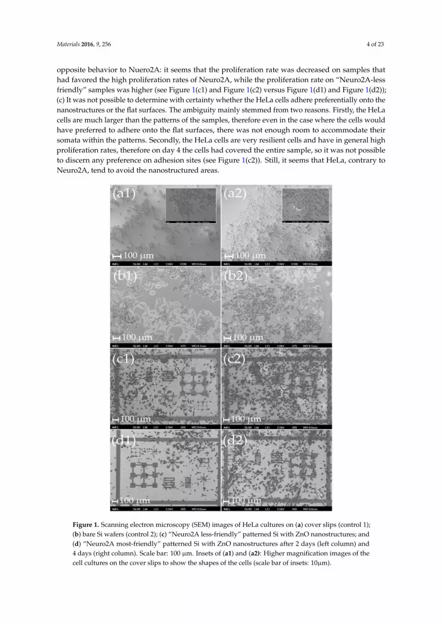
Materials 2016, 9, 256 4 of 23
opposite behavior to Nuero2A: it seems that the proliferation rate was decreased on samples thathad favored the high proliferation rates of Neuro2A, while the proliferation rate on “Neuro2A-lessfriendly” samples was higher (see Figure 1(c1) and Figure 1(c2) versus Figure 1(d1) and Figure 1(d2));(c) It was not possible to determine with certainty whether the HeLa cells adhere preferentially onto thenanostructures or the flat surfaces. The ambiguity mainly stemmed from two reasons. Firstly, the HeLacells are much larger than the patterns of the samples, therefore even in the case where the cells wouldhave preferred to adhere onto the flat surfaces, there was not enough room to accommodate theirsomata within the patterns. Secondly, the HeLa cells are very resilient cells and have in general highproliferation rates, therefore on day 4 the cells had covered the entire sample, so it was not possibleto discern any preference on adhesion sites (see Figure 1(c2)). Still, it seems that HeLa, contrary toNeuro2A, tend to avoid the nanostructured areas.
Materials 2016, 9, 256 4 of 24
(c) It was not possible to determine with certainty whether the HeLa cells adhere preferentially onto
the nanostructures or the flat surfaces. The ambiguity mainly stemmed from two reasons. Firstly, the
HeLa cells are much larger than the patterns of the samples, therefore even in the case where the
cells would have preferred to adhere onto the flat surfaces, there was not enough room to
accommodate their somata within the patterns. Secondly, the HeLa cells are very resilient cells and
have in general high proliferation rates, therefore on day 4 the cells had covered the entire sample, so
it was not possible to discern any preference on adhesion sites (see Figure 1(c2)). Still, it seems that
HeLa, contrary to Neuro2A, tend to avoid the nanostructured areas.
For that reason, the experiments were repeated with other types of patterns, which were not
only larger, but had larger flat surfaces compared to the samples used for the Neuro2A cultures and
in the first part of this work (hereafter referred to as samples “L” to distinguish them from the
samples of smaller patterns hereafter referred to as samples “S”). As seen in Figure 2, when larger
patterns were employed, the HeLa cells tended to move towards the flat surfaces and avoided the
nanostructures as evidenced by their somata that conformed to the shapes of the patterns.
Figure 1. Scanning electron microscopy (SEM) images of HeLa cultures on (a) cover slips (control 1);
(b) bare Si wafers (control 2); (c) “Neuro2A less-friendly” patterned Si with ZnO nanostructures; and
(d) “Neuro2A most-friendly” patterned Si with ZnO nanostructures after 2 days (left column) and 4
days (right column). Scale bar: 100 μm. Insets of (a1) and (a2): Higher magnification images of the cell
cultures on the cover slips to show the shapes of the cells (scale bar of insets: 10μm).
Figure 1. Scanning electron microscopy (SEM) images of HeLa cultures on (a) cover slips (control 1);(b) bare Si wafers (control 2); (c) “Neuro2A less-friendly” patterned Si with ZnO nanostructures; and(d) “Neuro2A most-friendly” patterned Si with ZnO nanostructures after 2 days (left column) and4 days (right column). Scale bar: 100 µm. Insets of (a1) and (a2): Higher magnification images of thecell cultures on the cover slips to show the shapes of the cells (scale bar of insets: 10µm).

Materials 2016, 9, 256 5 of 23
For that reason, the experiments were repeated with other types of patterns, which were not onlylarger, but had larger flat surfaces compared to the samples used for the Neuro2A cultures and in thefirst part of this work (hereafter referred to as samples “L” to distinguish them from the samples ofsmaller patterns hereafter referred to as samples “S”). As seen in Figure 2, when larger patterns wereemployed, the HeLa cells tended to move towards the flat surfaces and avoided the nanostructures asevidenced by their somata that conformed to the shapes of the patterns.Materials 2016, 9, 256 5 of 24
Figure 2. SEM images of (a) of the patterned Si wafer with larger patterns and larger flat areas (the
darker areas contain the ZnO nanorods shown in the zoom-in inset image; scale bar: 100 nm); (b) the
same samples with HeLa cells after 4 days in culture, where one can see that the cells mostly adhere
onto the flat areas (the white areas are the nanorods that have been covered by salts from the nutrient
medium that was not fully removed after washing). Scale bar: 100 μm.
2.2. HeLa Cultures on Si3N4
Within this work, effort was also put in to create cellular networks on materials that are
commonly used for optical biosensing applications and more specifically in label-free optical
biosensors. One of the most common materials used for waveguides is silicon nitride (Si3N4).
Towards that purpose Si3N4 layers were deposited onto conventional 3”- and 4”-Si wafers and
subsequently were patterned and modified with ZnO nanostructures in a similar way to the one
employed for Si wafers (for details please refer to Section 4). The cultures followed the same
protocols as the ones used for the Si substrates. Both types of patterns, smaller and larger ones were
used in an analogous way to the Si substrates.
As seen in Figure 3, the HeLa cells preferentially adhered onto the flat nitride surfaces as soon
as day 2. They appeared to conform to the shape of the patterns and to adhere onto the borderlines.
Even in the case of samples “S” of limited free areas, the cells seem to try to squeeze inside the
patterns so as to avoid the nanostructured surfaces. In addition, on day 4 the cells that were forced to
sit on the nanostructured areas because of the fast proliferation rates, obtained a more spherical
shape than their usual elongated one (see Figure 3(b2) and Figure 3(c2)).
When type “L” samples (large patterns and large flat areas) were employed as substrates, the
preferential adhesion of the HeLa cells onto the flat areas was evident even from day 2 (Figure 4). On
day 4, because of the very large cell population, numerous cells seem to be “forcibly” located onto
the nanostructures, but they were fewer in number and their shape more spherical as was the case
with type “S” templates. Again, after 4 days the cells appear rounder and do not have the usual
oblong shape observed when cultured on flat surfaces (like conventional petri dishes or cover slips).
It was very interesting to note that the cells that adhered onto the flat areas had a very large number
of extended filopodia and were flat in shape (Figure 5). It seems that the flat areas provide a more
favorable ground for the HeLa cells to create focal adhesions than the nanostructures.
Figure 2. SEM images of (a) of the patterned Si wafer with larger patterns and larger flat areas (thedarker areas contain the ZnO nanorods shown in the zoom-in inset image; scale bar: 100 nm); (b) thesame samples with HeLa cells after 4 days in culture, where one can see that the cells mostly adhereonto the flat areas (the white areas are the nanorods that have been covered by salts from the nutrientmedium that was not fully removed after washing). Scale bar: 100 µm.
2.2. HeLa Cultures on Si3N4
Within this work, effort was also put in to create cellular networks on materials that are commonlyused for optical biosensing applications and more specifically in label-free optical biosensors. Oneof the most common materials used for waveguides is silicon nitride (Si3N4). Towards that purposeSi3N4 layers were deposited onto conventional 3”- and 4”-Si wafers and subsequently were patternedand modified with ZnO nanostructures in a similar way to the one employed for Si wafers (for detailsplease refer to Section 4). The cultures followed the same protocols as the ones used for the Si substrates.Both types of patterns, smaller and larger ones were used in an analogous way to the Si substrates.
As seen in Figure 3, the HeLa cells preferentially adhered onto the flat nitride surfaces as soon asday 2. They appeared to conform to the shape of the patterns and to adhere onto the borderlines. Evenin the case of samples “S” of limited free areas, the cells seem to try to squeeze inside the patterns soas to avoid the nanostructured surfaces. In addition, on day 4 the cells that were forced to sit on thenanostructured areas because of the fast proliferation rates, obtained a more spherical shape than theirusual elongated one (see Figure 3(b2) and Figure 3(c2)).
When type “L” samples (large patterns and large flat areas) were employed as substrates, thepreferential adhesion of the HeLa cells onto the flat areas was evident even from day 2 (Figure 4).On day 4, because of the very large cell population, numerous cells seem to be “forcibly” locatedonto the nanostructures, but they were fewer in number and their shape more spherical as was thecase with type “S” templates. Again, after 4 days the cells appear rounder and do not have the usualoblong shape observed when cultured on flat surfaces (like conventional petri dishes or cover slips).It was very interesting to note that the cells that adhered onto the flat areas had a very large numberof extended filopodia and were flat in shape (Figure 5). It seems that the flat areas provide a morefavorable ground for the HeLa cells to create focal adhesions than the nanostructures.

Materials 2016, 9, 256 6 of 23
Materials 2016, 9, 256 6 of 24
Figure 3. (a); (b) SEM images at two different magnifications (scale bars: 100 μm and 10 μm,
respectively) and (c) optical microscope images of HeLa cells after 2 days (left column), and 4 days
(right column) in culture on modified nitride samples “S” with small free patterns, where it can be
seen that despite the limited flat surface the cells tend to avoid the nanostructured areas and try to
“squeeze” inside the patterns. On day 4, the cells that adhered onto the nanostructures were no
longer elongated and obtained a more spherical shape. (a1); (b1); and (c1) were obtained after 2 days
in culture, while (a2); (b2); and (c2) were obtained after 4 days in culture.
Figure 3. (a); (b) SEM images at two different magnifications (scale bars: 100 µm and 10 µm,respectively) and (c) optical microscope images of HeLa cells after 2 days (left column), and 4 days(right column) in culture on modified nitride samples “S” with small free patterns, where it can be seenthat despite the limited flat surface the cells tend to avoid the nanostructured areas and try to “squeeze”inside the patterns. On day 4, the cells that adhered onto the nanostructures were no longer elongatedand obtained a more spherical shape. (a1); (b1); and (c1) were obtained after 2 days in culture, while(a2); (b2); and (c2) were obtained after 4 days in culture.
As a conclusion, the HeLa cells tend to adhere preferentially onto flat areas when nitridelayers are modified with ZnO nanostructures. In a recent publication by Migliorini et al. [61], itis suggested that the controlling factor in cellular adhesion might not be the nanostructuring itself butthe mechanical properties of the substrata. This point is further analyzed in Section 3. Nonetheless,even in the case of modified nitride layers, the method seems to be very promising for culturing cellson predefined patterns.
2.3. HeLa Cultures on Emulated MEAs
Third types of sample realized with the proposed methodology were emulated microelectrodearrays (MEAs). In essence, Si 3”- and 4”-wafers were patterned with Al and Pt layers on top of whichZnO nanostructures were grown via the hydrothermal method (see Section 3 for fabrication details)emulating electrodes that could be locally modified with nanoarchitectures. Again, HeLa cells werecultured for up to 4 days and observed on day 2 and day 4, under exactly the same conditions as inSections 2.1 and 2.2. The results are summarized in Figures 6 and 7.

Materials 2016, 9, 256 7 of 23Materials 2016, 9, 256 7 of 24
Figure 4. Optical microscope images of HeLa cells on various patterns after (a) 2 days; and (b) 4 days
in culture on modified nitride samples “L” with large patterns and large flat areas showing the
preference of the cells to adhere onto the flat surfaces avoiding the nanostructures. (a1); (a2); and (a3)
were obtained at several locations of the template after 2 days in culture. (b1); (b2); and (b3) were
obtained at several locations of the template after 4 days in culture.
Figure 5. High magnification (×100) optical microscope images in dark field of HeLa cells after 4 days
in culture on modified nitride samples that have adhered (a) on the nitride surface; and (b) onto the
nanostructures. In (a), one can see the extensive filopodia network, while in (b) the more spherical
shape of the cells can be discerned. The colorful specs are the tips of the ZnO nanostructures as seen
in dark field.
Figure 4. Optical microscope images of HeLa cells on various patterns after (a) 2 days; and (b) 4 days inculture on modified nitride samples “L” with large patterns and large flat areas showing the preferenceof the cells to adhere onto the flat surfaces avoiding the nanostructures. (a1); (a2); and (a3) wereobtained at several locations of the template after 2 days in culture. (b1); (b2); and (b3) were obtainedat several locations of the template after 4 days in culture.
Materials 2016, 9, 256 7 of 24
Figure 4. Optical microscope images of HeLa cells on various patterns after (a) 2 days; and (b) 4 days
in culture on modified nitride samples “L” with large patterns and large flat areas showing the
preference of the cells to adhere onto the flat surfaces avoiding the nanostructures. (a1); (a2); and (a3)
were obtained at several locations of the template after 2 days in culture. (b1); (b2); and (b3) were
obtained at several locations of the template after 4 days in culture.
Figure 5. High magnification (×100) optical microscope images in dark field of HeLa cells after 4 days
in culture on modified nitride samples that have adhered (a) on the nitride surface; and (b) onto the
nanostructures. In (a), one can see the extensive filopodia network, while in (b) the more spherical
shape of the cells can be discerned. The colorful specs are the tips of the ZnO nanostructures as seen
in dark field.
Figure 5. High magnification (ˆ100) optical microscope images in dark field of HeLa cells after 4 daysin culture on modified nitride samples that have adhered (a) on the nitride surface; and (b) onto thenanostructures. In (a), one can see the extensive filopodia network, while in (b) the more sphericalshape of the cells can be discerned. The colorful specs are the tips of the ZnO nanostructures as seen indark field.

Materials 2016, 9, 256 8 of 23
Materials 2016, 9, 256 8 of 24
As a conclusion, the HeLa cells tend to adhere preferentially onto flat areas when nitride layers
are modified with ZnO nanostructures. In a recent publication by Migliorini et al. [61], it is suggested
that the controlling factor in cellular adhesion might not be the nanostructuring itself but the
mechanical properties of the substrata. This point is further analyzed in Section 3. Nonetheless, even
in the case of modified nitride layers, the method seems to be very promising for culturing cells on
predefined patterns.
2.3. HeLa Cultures on Emulated MEAs
Third types of sample realized with the proposed methodology were emulated microelectrode
arrays (MEAs). In essence, Si 3”- and 4”-wafers were patterned with Al and Pt layers on top of which
ZnO nanostructures were grown via the hydrothermal method (see Section 3 for fabrication details)
emulating electrodes that could be locally modified with nanoarchitectures. Again, HeLa cells were
cultured for up to 4 days and observed on day 2 and day 4, under exactly the same conditions as in
Section 2.1 and Section 2.2. The results are summarized in Figures 6 and 7.
Figure 6. SEM images of HeLa cells on various patterns cultured on Al-MEAs after (a) 2 days; and
(b) 4 days in culture where it can be seen that after day 2 the cells move preferentially to the
nanostructured metallic patterns. Scale bar: 100 μm. (a1); (a2); and (a3) were obtained at several
locations of the template after 2 days in culture. (b1); (b2); and (b3) were obtained at several locations
of the template after 4 days in culture.
Figure 6. SEM images of HeLa cells on various patterns cultured on Al-MEAs after (a) 2 days;and (b) 4 days in culture where it can be seen that after day 2 the cells move preferentially to thenanostructured metallic patterns. Scale bar: 100 µm. (a1); (a2); and (a3) were obtained at severallocations of the template after 2 days in culture. (b1); (b2); and (b3) were obtained at several locationsof the template after 4 days in culture.
On these templates, the HeLa cells—in stark contrast to modified Si and Si3N4 substrates—clearlyformed networks on the predefined patterns seemingly guided by nanomechanical cues from thenanostructures. It was striking that until day 2 the cells just proliferated and adhered non-preferentiallyonto the flat surfaces and the nanostructured metallic patterns. However, between day 2 and 4,they migrated onto the nanostructured areas conforming totally to the patterns, as can be seen inFigures 6 and 7 for the Al-MEAs and Pt-MEAs, respectively. It was also very interesting to notice thatwhen there were lithographic imperfections the cells would still conform to the patterns and wouldnot adhere to the flat surfaces (see for example Figure 6(b3)).
The results in the case of HeLa support the great potential of the method to be applied or controlledcellular cultures for HeLa cells. The cells are guided through the nanomechanical cues to specifiedpatterns and a plethora of applications (ranging from single-cell observations and electrophysiologyexperiments to pharmacological studies) can be envisaged.

Materials 2016, 9, 256 9 of 23
Materials 2016, 9, 256 9 of 24
On these templates, the HeLa cells—in stark contrast to modified Si and Si3N4 substrates—clearly
formed networks on the predefined patterns seemingly guided by nanomechanical cues from the
nanostructures. It was striking that until day 2 the cells just proliferated and adhered
non-preferentially onto the flat surfaces and the nanostructured metallic patterns. However,
between day 2 and 4, they migrated onto the nanostructured areas conforming totally to the
patterns, as can be seen in Figures 6 and 7 for the Al-MEAs and Pt-MEAs, respectively. It was also
very interesting to notice that when there were lithographic imperfections the cells would still
conform to the patterns and would not adhere to the flat surfaces (see for example Figure 6(b3)).
The results in the case of HeLa support the great potential of the method to be applied or
controlled cellular cultures for HeLa cells. The cells are guided through the nanomechanical cues to
specified patterns and a plethora of applications (ranging from single-cell observations and
electrophysiology experiments to pharmacological studies) can be envisaged.
Figure 7. SEM and optical microscope images of HeLa cells cultured on Pt-MEAs after (a) 2 days
(image a2: dark field, magnification 10/ image a3: dark field, magnification 50); and (b) 4 days in
culture where it can be seen that after day 2 the cells move preferentially to the nanostructured
metallic patterns. (a1); (a2); and (a3) were obtained at several locations of the template after 2 days in
culture. (b1); (b2); and (b3) were obtained at several locations of the template after 4 days in culture.
2.4. HeLa Cultures on Conventional Cover Slips
As a final type of substrate with hydrothermally-grown ZnO nanostructures, conventional
cover slips were also chosen. The reason behind this option was that cover slips are commonly used
Figure 7. SEM and optical microscope images of HeLa cells cultured on Pt-MEAs after (a) 2 days(image a2: dark field, magnification ˆ 10/ image a3: dark field, magnification ˆ 50); and (b) 4 days inculture where it can be seen that after day 2 the cells move preferentially to the nanostructured metallicpatterns. (a1); (a2); and (a3) were obtained at several locations of the template after 2 days in culture.(b1); (b2); and (b3) were obtained at several locations of the template after 4 days in culture.
2.4. HeLa Cultures on Conventional Cover Slips
As a final type of substrate with hydrothermally-grown ZnO nanostructures, conventional coverslips were also chosen. The reason behind this option was that cover slips are commonly used inseveral optical methods for real-time recording of cells (like OWLS and in general video microscopy).Patterning of glass proved to be more challenging than anticipated and is analyzed in detail in Section 4.As a first step, cover slips uniformly covered with ZnO nanostructures were studied and compared tobare cover slips and Si wafers that were used as controls, since the results of Sections 2.1 and 2.2 hadshown that the ZnO nanostructures are not favorable to cell attachment. The initial cell populationwas 125 k/sample and the cells were examined after 1 and 2 days.
Already at day 1, it was obvious that the HeLa cells could not easily adhere onto the ZnOnanostructures as evidenced by the decreased population compared to the controls as well as theirspherical shape (Figure 8). On day 2, while the control samples were fully covered with cells, themodified cover slips had cells that seemed to have undergone necrosis. It was also observed that deadcells were floating on the culture medium in the petri dish.

Materials 2016, 9, 256 10 of 23
Materials 2016, 9, 256 10 of 24
in several optical methods for real-time recording of cells (like OWLS and in general video
microscopy). Patterning of glass proved to be more challenging than anticipated and is analyzed in
detail in Section 4. As a first step, cover slips uniformly covered with ZnO nanostructures were
studied and compared to bare cover slips and Si wafers that were used as controls, since the results
of Section 2.1 and Section 2.2 had shown that the ZnO nanostructures are not favorable to cell
attachment. The initial cell population was 125 k/sample and the cells were examined after 1 and 2 days.
Already at day 1, it was obvious that the HeLa cells could not easily adhere onto the ZnO
nanostructures as evidenced by the decreased population compared to the controls as well as their
spherical shape (Figure 8). On day 2, while the control samples were fully covered with cells, the
modified cover slips had cells that seemed to have undergone necrosis. It was also observed that
dead cells were floating on the culture medium in the petri dish.
Figure 8. Optical microscope images (phase contrast images) of HeLa cells on (a1) control cover slips;
(b1) bare Si; and (c1) cover slips covered with ZnO nanostructures after 24 h in culture; and (a2)
control cover slips; (b2) bare Si; and (c2) cover slips covered with ZnO nanostructures after 48 h in
culture. It is evident that the cells cannot adhere onto the ZnO nanostructures and undergo necrosis
even from day 1.
As a next step, patterned cover slips were employed. Two types of patterning were used, one in
which the cover slips were coated with ZnO nanostructures with only small flat patterns in between,
and the exact negative i.e. bare cover slip with small patterns containing the nanorods (see Figure 13a
and 13b in Section 4). The cells were cultured for 48 h in total, but were checked under an optical
microscope at 24 h, and then the culture was continued until 48 h, when the cells were fixed. At 24 h
there was no evidence of preferred adhesion and the cells could be seen everywhere on both samples
(Figure 9(a1,b1)). At 48 h though, as expected, the cells on the sample which in the most part was
covered with ZnO, underwent necrosis (Figure 9(a2)), while the cells on the “negatively-patterned”
cover slips migrated and conformed to the patterns (Figure 9(b2)).
Figure 8. Optical microscope images (phase contrast images) of HeLa cells on (a1) control cover slips;(b1) bare Si; and (c1) cover slips covered with ZnO nanostructures after 24 h in culture; and (a2) controlcover slips; (b2) bare Si; and (c2) cover slips covered with ZnO nanostructures after 48 h in culture.It is evident that the cells cannot adhere onto the ZnO nanostructures and undergo necrosis evenfrom day 1.
As a next step, patterned cover slips were employed. Two types of patterning were used,one in which the cover slips were coated with ZnO nanostructures with only small flat patternsin between, and the exact negative i.e. bare cover slip with small patterns containing the nanorods(see Figures 13a and 13b in Section 4). The cells were cultured for 48 h in total, but were checked underan optical microscope at 24 h, and then the culture was continued until 48 h, when the cells were fixed.At 24 h there was no evidence of preferred adhesion and the cells could be seen everywhere on bothsamples (Figure 9(a1,b1)). At 48 h though, as expected, the cells on the sample which in the most partwas covered with ZnO, underwent necrosis (Figure 9(a2)), while the cells on the “negatively-patterned”cover slips migrated and conformed to the patterns (Figure 9(b2)).
These results show the great potential of nanopatterned cover slips for engineered cellularstructures. The extremely low cost of the substrates and the equally low cost of the method make it avery promising route for a viable commercial product.

Materials 2016, 9, 256 11 of 23
Materials 2016, 9, 256 11 of 24
These results show the great potential of nanopatterned cover slips for engineered cellular
structures. The extremely low cost of the substrates and the equally low cost of the method make it a
very promising route for a viable commercial product.
Figure 9. Optical microscope images (phase contrast images) of HeLa cells on (a1) a cover slip
covered with ZnO nanostructures with small free (flat) patterns; and (b1) cover slip with ZnO
nanostructures only on top of the small square lattice patterns after 24 h in culture; (a2) a cover slip
covered with ZnO nanostructures with small free (flat) patterns; and (b2) cover slip with ZnO
nanostructures only on top of the small square lattice patterns, after 48 h in culture. It is evident that
the cells undergo necrosis after 24 h on the coverslips with the large patterns a1), while when the
patterns are small (b2) there is total conformation of the cell somata to the borders of the patterns
between day 1 and day 2.
3. Discussion
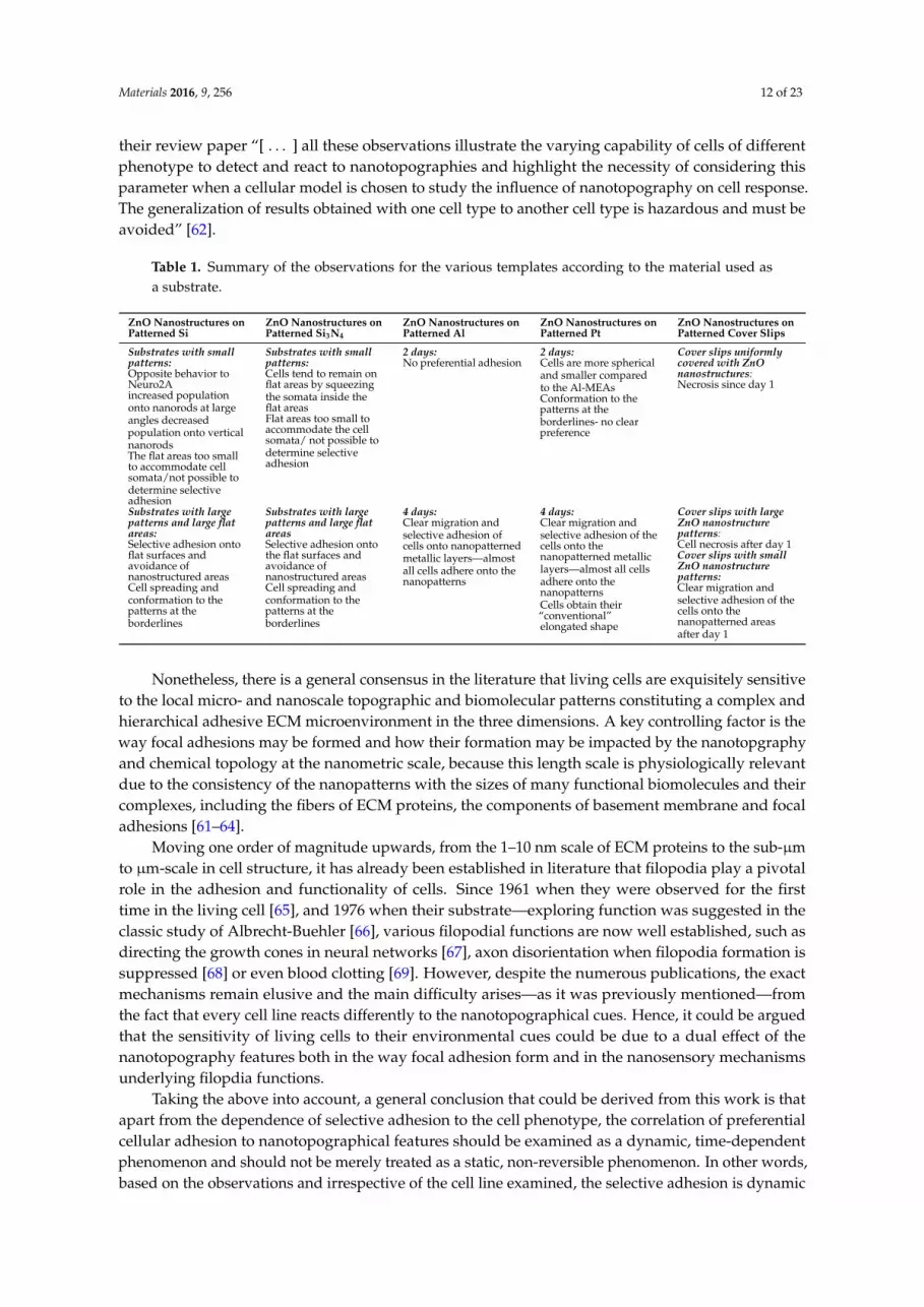
For clarity reasons, and to facilitate the analysis and comparison of the results, the main
observations have been summarized in Table 1. As a general conclusion, the proposed methodology
seems very promising for the realization of cost-efficient templates for engineered cellular networks
through the use of nanomechanical and nanotopographical cues onto a variety of substrates that can
be applied to MEAs as well as optical biosensors. Still, one important parameter is the cell phenotype
and it should be taken into account—as also seen in literature—that there is no universal
nanotopographical feature that can regulate in a unique way the behavior of any cell type. Under
this light, it is important to note beforehand that the results of this work may conflict with other
reports in the literature or could potentially be entirely different if the templates were employed
with other cell types.
Figure 9. Optical microscope images (phase contrast images) of HeLa cells on (a1) a cover slip coveredwith ZnO nanostructures with small free (flat) patterns; and (b1) cover slip with ZnO nanostructuresonly on top of the small square lattice patterns after 24 h in culture; (a2) a cover slip covered with ZnOnanostructures with small free (flat) patterns; and (b2) cover slip with ZnO nanostructures only on topof the small square lattice patterns, after 48 h in culture. It is evident that the cells undergo necrosisafter 24 h on the coverslips with the large patterns a1), while when the patterns are small (b2) there istotal conformation of the cell somata to the borders of the patterns between day 1 and day 2.
3. Discussion
For clarity reasons, and to facilitate the analysis and comparison of the results, the mainobservations have been summarized in Table 1. As a general conclusion, the proposed methodologyseems very promising for the realization of cost-efficient templates for engineered cellular networksthrough the use of nanomechanical and nanotopographical cues onto a variety of substrates that can beapplied to MEAs as well as optical biosensors. Still, one important parameter is the cell phenotype andit should be taken into account—as also seen in literature—that there is no universal nanotopographicalfeature that can regulate in a unique way the behavior of any cell type. Under this light, it is importantto note beforehand that the results of this work may conflict with other reports in the literature orcould potentially be entirely different if the templates were employed with other cell types.
Despite the fact that the cellular networks were not realized in all types of templates, there werestrong indications that ZnO nanostructures can induce selective cellular adhesion and can guide HeLacells onto predefined patterns and induce their adhesion on selected topographies. Given the low costand the CMOS-compatibility of the method, the proposed methodology has a great potential to beused for viable products spanning from microelectrode arrays to modified optical sensors and reallylow-cost modified cover slips for real-time monitoring applications.
Coming to interpret the results per fabricated template, one should take into account that thecell guidance through nanomechanical cues is still an open issue in the literature, despite the largenumber of publications and studies. One difficulty in defining the controlling factors is that everypublication employs different types of substrates, various micro/nanotopographical features, and mostimportantly different cell lines. In several cases, the findings of researchers may be contradictory, aswas also the case in this work compared to [57] or from type of substrate to substrate within this work(e.g. modified Si and Si3N4 versus the emulated MEAs). Moreover, different cell lines react differentlyto the nanotopography and may have exactly the opposite responses. As Anselme et al. pointed out in
Materials 2016, 9, 256 12 of 23
their review paper “[ . . . ] all these observations illustrate the varying capability of cells of differentphenotype to detect and react to nanotopographies and highlight the necessity of considering thisparameter when a cellular model is chosen to study the influence of nanotopography on cell response.The generalization of results obtained with one cell type to another cell type is hazardous and must beavoided” [62].
Table 1. Summary of the observations for the various templates according to the material used asa substrate.
ZnO Nanostructures onPatterned Si
ZnO Nanostructures onPatterned Si3N4
ZnO Nanostructures onPatterned Al
ZnO Nanostructures onPatterned Pt
ZnO Nanostructures onPatterned Cover Slips
Substrates with smallpatterns:Opposite behavior toNeuro2Aincreased populationonto nanorods at largeangles decreasedpopulation onto verticalnanorodsThe flat areas too smallto accommodate cellsomata/not possible todetermine selectiveadhesion
Substrates with smallpatterns:Cells tend to remain onflat areas by squeezingthe somata inside theflat areasFlat areas too small toaccommodate the cellsomata/ not possible todetermine selectiveadhesion
2 days:No preferential adhesion
2 days:Cells are more sphericaland smaller comparedto the Al-MEAsConformation to thepatterns at theborderlines- no clearpreference
Cover slips uniformlycovered with ZnOnanostructures:Necrosis since day 1
Substrates with largepatterns and large flatareas:Selective adhesion ontoflat surfaces andavoidance ofnanostructured areasCell spreading andconformation to thepatterns at theborderlines
Substrates with largepatterns and large flatareasSelective adhesion ontothe flat surfaces andavoidance ofnanostructured areasCell spreading andconformation to thepatterns at theborderlines
4 days:Clear migration andselective adhesion ofcells onto nanopatternedmetallic layers—almostall cells adhere onto thenanopatterns
4 days:Clear migration andselective adhesion of thecells onto thenanopatterned metalliclayers—almost all cellsadhere onto thenanopatternsCells obtain their“conventional”elongated shape
Cover slips with largeZnO nanostructurepatterns:Cell necrosis after day 1Cover slips with smallZnO nanostructurepatterns:Clear migration andselective adhesion of thecells onto thenanopatterned areasafter day 1
Nonetheless, there is a general consensus in the literature that living cells are exquisitely sensitiveto the local micro- and nanoscale topographic and biomolecular patterns constituting a complex andhierarchical adhesive ECM microenvironment in the three dimensions. A key controlling factor is theway focal adhesions may be formed and how their formation may be impacted by the nanotopgraphyand chemical topology at the nanometric scale, because this length scale is physiologically relevantdue to the consistency of the nanopatterns with the sizes of many functional biomolecules and theircomplexes, including the fibers of ECM proteins, the components of basement membrane and focaladhesions [61–64].
Moving one order of magnitude upwards, from the 1–10 nm scale of ECM proteins to the sub-µmto µm-scale in cell structure, it has already been established in literature that filopodia play a pivotalrole in the adhesion and functionality of cells. Since 1961 when they were observed for the firsttime in the living cell [65], and 1976 when their substrate—exploring function was suggested in theclassic study of Albrecht-Buehler [66], various filopodial functions are now well established, such asdirecting the growth cones in neural networks [67], axon disorientation when filopodia formation issuppressed [68] or even blood clotting [69]. However, despite the numerous publications, the exactmechanisms remain elusive and the main difficulty arises—as it was previously mentioned—fromthe fact that every cell line reacts differently to the nanotopographical cues. Hence, it could be arguedthat the sensitivity of living cells to their environmental cues could be due to a dual effect of thenanotopography features both in the way focal adhesion form and in the nanosensory mechanismsunderlying filopdia functions.
Taking the above into account, a general conclusion that could be derived from this work is thatapart from the dependence of selective adhesion to the cell phenotype, the correlation of preferentialcellular adhesion to nanotopographical features should be examined as a dynamic, time-dependentphenomenon and should not be merely treated as a static, non-reversible phenomenon. In other words,based on the observations and irrespective of the cell line examined, the selective adhesion is dynamic

Materials 2016, 9, 256 13 of 23
and the cells—which are in essence living organisms—continually react and adapt to their externalmicro/nano-environment. Hence, even though specific patterns and nanostructures were identified assubstrates that can lead to selective adhesion and cellular network formation, time is a very importantparameter and apart from the optimum geometry per cell line, the optimum culturing time must beidentified as well.
This conclusion seems to be in agreement with the recent publication of Albuschies and Vogel [70].Based on their study, the authors have developed a model describing the way the filopodia explorethe topography of their environment and can adhere or not onto the substrates. Filopodia anchorageis a dynamic phenomenon and depends on the dynamics of contact angle formed towards flexibleobjects. It is this angle that defines whether the contact can be mechanically stabilized or peeled off.According to this zipping mechanism—as termed by the authors—topographical preference is notjust an intrinsic and cell specific attribute. Instead, topographical preferences can change with time.Contact guidance might be a filopodia traction force-mediated peeling process. The cell is guided onlyin the direction where the geometrical constraints allow the filopodial contacts to mature by forminga maximum number of adhesive bonds. The contact angle formed between a filopodium and anyobject determines whether the contact can be stabilized or broken. Any synthetic of biological fiberfree to swing around and align with filopodia will evoke a greatly different mechanosensation thanbulk materials or interconnected fiber networks.
These conclusions are also in agreement with reference [71], where the time-dependence ofselective adhesion was reported. The authors observed that cells that were initially adhered on specificnanotopographies migrated to “less-friendly” nanotopographies after a few days. It was also observedthat the closer the “less-friendly” areas were to the preferred ones the faster they would fill with cells.In addition, a large number of cells would sit on the borderlines between the two areas early on in thecultures. The authors established that the cells that had selectively adhered onto the nanotopographiest enhanced anchorage synthesized ECM proteins, i.e. acted as “ECM sources”. ECM spreading, startingat the borderline between the two nanoscale topographies, increasingly masked the “unfavorable”nanotopography and enhanced cell adhesion. In other words, the initial cell adhesion and spreadingwere predominantly dependent on the nanotopography and the less-favorable areas could be “rescued”at least partially by ECM spread out of the adhered cells, which could then migrate in a step-by-stepmanner with the support of the ECM produced previously on the friendly nanotopography.
The behavior of both Neuro2A cells in [57] and HeLa cells reported in this work wereanalogous. Irrespective of which topography the cells preferentially adhere to (Neuro2A favorvertical nanorods, while HeLa prefer the flat surfaces or the nanostructured metallic layers) there isa clear time-dependence of the phenomenon. In particular, in the case of HeLa cells, the adhesion ispreferential towards the flat surfaces (when the substrate is Si or Si3N4) and it seems that the cellstend to avoid the nanostructures. Noticeably enough, the more “Neuro2A-friendlier” a surface is, theless “HeLa-friendly” it becomes: the vertical nanorods are the areas that HeLa cells tend to avoid themost, while on the large-angled nanorods they have an “intermediate” behavior. Intense filopodiaextension was observed only on the flat surfaces (Figure 5a). After day 2, the cells that have sat onthe nanostructures lose their elongated shape and become rounder, indicative of necrosis (Figure 5b).This observation was further substantiated by the necrosis of HeLa cells cultured on the modifiedcover slips. Therefore, the particular nanotopography offered by ZnO nanorods does not promote thecreation of focal adhesions for this cell line. In contrast, the HeLa behavior was exactly the oppositewhen cultured on the emulated MEAs. In this case, the HeLa cells adhered selectively onto thenanopatterned metallic layers conforming totally to the shape of the patterns. It must be underlinedthat the selective adhesion required 4 days to be realized as fully supporting the scenario of the celldynamical behavior and rendering the culture duration as one of the controlling factors.
Of course, although the trends of adhesion selectivity are clearly visible, more work is requiredto reveal the underlying biological and biophysical mechanisms. Details such as the effects of ZnOsurface nanostructuring, structure thickness and geometry on contact angle, and protein adsorption

Materials 2016, 9, 256 14 of 23
should be systematically investigated. These experiments are outside the scope of the present work,but using the developed methodologies could be carried out in a straightforward way, even usinghigh throughput measuring formats. Further improvement of the performance and specificity couldbe obtained by combining the developed structures with cost-effective polymer or protein coatingscontaining one or more cell adhesion motifs.
In summary, the suggested methodology is extremely promising for the creation of engineeredcellular networks through purely nanomechanical cues. One of the most important results of this studywas a better understanding of the dynamics of selective cellular adhesion and the implication of timeas a controlling factor that must be combined with nanomechanosensation. Future studies that areenvisaged are the real-time monitoring of cell adhesion in order to further elucidate the phenomenon,and the application of the proposed templates to other cell lines and the realization of co-cultures.Finally, further studies are foreseen for the evolvement of the method into a technology that can bereadily transferred to mass-production and the development of real-life viable products.
4. Materials and Methods
4.1. Short Description of Sol-Gel/Hydrothermal Methodology
The suggested methodology has been widely used over the past ten years and was opted notonly because of its versatility, but also for the following competitive advantages that it possessesover other fabrication methods: (a) it is facile, time-efficient and of very low cost, (b) clean-roomconditions are not necessary, (c) it allows the control of the nanostructure morphology through simplekey parameters (e.g. composition of the sol-gel, annealing temperature and duration, the nutrientsolution concentration, pH and temperature, the growth duration etc.), (d) it is CMOS-compatibleand can be integrated with standard microfabrication techniques, (e) it can be applied to a plethora ofsubstrates, (f) it is non-hazardous and environmentally-friendly.
In essence, the method consists of two steps:
1. the deposition of a thin seeding (nucleation) layer that provides the necessary nucleation sitesfor the nanocrystal formation to commence. The deposition of the seeding layer is achievedvia simple centrifugation of an appropriately selected sol-gel formed by the dissolution ofzinc acetate dihydrate into an alcohol (ethanol or propanol), which may contain ethanolamineor triethylamine that promotes the formation of ZnO nanoparticles. It has been establishedthat the seeding layer has a direct and critical effect on the structural properties of the ZnOnanostructures that are subsequently grown on top of it controlling the alignment, density, andmorphological characteristics of the resulting structures. In other words, the seeding layerpreparation conditions have a direct impact on the resulting structures and one can tailorthem according to the targeted applications through several parameters like the number ofspin-coatings, the annealing temperature and duration [29,72,73].
2. the hydrothermal growth step per se, during which the substrates are either immersed or floatingin the nutrient solution most commonly constituted of (as in our case) zinc nitrate hexahydrate(ZnNO3.6H2O) and hexamethylentetramine (C6H12N4, HMTA) [28]. The nutrient solution isheated and the formation of the ZnO nanostructures is achieved through the following reactionstaking place over the nucleation sites of the seeding layer:
C6H12N4 ` 6H2OÑ 6HCHO ` 4NH3 (1)
NH3 ` H2OÑNH4+ ` OH- (2)
Zn2+ ` 4OH-ÑrZnpOHq4s2+ (3)
rZnpOHq4s2+ÑZnO22- ` 2H2O (4)
Zn2+surface ` ZnO2
2-solutionÑ 2ZnO (5)

Materials 2016, 9, 256 15 of 23
O2-surface ` ZnO2
2-solution ` H2OÑZnO ` 4OH- (6)
The role of HMTA has still not been fully elucidated. It is generally believed that it acts as anonionic cyclic tertiary amine and thus serves as a Lewis acid base to metal ions and as a bidentateligand capable of bridging two zinc ions in solution. The OH´ from the slow hydrolysis of HMTAassists the formation of the zinc hydroxide intermediate, which acts as a growth unit as shown inFormulas (2)–(4). The slow release of the hydroxyl groups may control the formation of the growingunits, thereby exerting a profound effect on controlling the growth process of ZnO NRs. Coordinationto the zinc of HMTA can also kinetically control the concentration of free zinc ion in solution andmaintain the warmth of the reaction environment. Ammonia is provided by slowly decomposingHMTA with gradually increasing temperature. Zn2+ is known to coordinate in tetrahedral complexes.Zn2+ ions are stored by forming complex zinc [Zn(OH)4]2+. When the reaction temperature rapidlyincreases, HMTA is quickly hydrolyzed and produces a large amount of OH´ in a short period. Largeamounts of ZnO nuclei form in the solution and aggregate together, thereby hindering the growthof ZnO NRs. Apart from the inherent rapid growth along the direction of the polar surfaces of thewurtzite ZnO crystal, the attachment of HMTA to the non-polar side facets also facilitate anisotropicgrowth in the [0001] direction. Thus, once the ZnO seeds are formed, the environment composed ofZn2+ and HMTA restrains the crosswise growth and guides the seeds to grow along the c-axis direction.
For each type of template fabricated in this work, appropriate sol-gels were selected and thevarious deposition conditions were tuned according to the substrate in order to achieve the desiredZnO nanostructure morphology. The hydrothermal growth step was kept the same for all templatesand it was a 2-h growth at 87 ˝C in a 40 mM equimolar solution of ZnNO3¨6H2O and HMTA.
4.2. Fabrication of Si and Si3N4 Templates with Patterns of ZnO Nanostructures
The process steps followed for the realization of Si and Si3N4 templates with patterns of ZnOnanostructures were identical and are schematically shown in Figure 10. Briefly, either bare Si or Siwafers covered with 100 nm-thick LP-CVD Si3N4 layer were cleaned with organic solvents and thenspin-coated with a sol-gel for the formation of the seeding layer. The sol-gel consisted of 40 mM zincacetate dihydrate (Zn(CH3COO)2.2H2O, Merck) dissolved in ethanol (C2H6O, Carlo Erba Reagents).The sol was prepared by vigorous stirring at 60 ˝C for 30 min and was employed after cooling atroom temperature. The solution was spin-coated onto the substrates several times with 10 min dryingsteps in air in between. Subsequently, the samples were annealed at 500 ˝C in an oven in the presenceof atmospheric air. Annealing for 1 h resulted in Si-templates with ZnO nanorods grown at largeangles (Neuro2A-unfriendly templates), while annealing for 2 h resulted in vertical densely-packedZnO nanorods (Neuro2a-friendly templates). The Si3N4 templates were all annealed for 2 h, sincethe scope of the study was to determine the effect of large versus small areas of nanostructures(see Section 2.2). After the seeding layer formation, optical lithography was performed in order todefine the patterns over which the ZnO nanostructures were to be grown. The lithographic step wasfollowed by the growth of the NWs at 87 ˝C in a 40 mM equimolar aqueous solution consisting of zincnitrate hexahydrate (N2O6Zn.6H2O, Sigma-Aldrich) and hexamethylenetetramine-HMTA ((CH2)6N4,Panreac) for 2 h. The samples were finally cleaned with DI water in an ultra-sonic bath for 30 min.Typical images of the prepared templates are shown in Figure 11a–c.
4.3. Fabrication of Templates with Metallic Patterns Modified with ZnO Nanostructures (Emulated MEAs)
The fabrication process of the emulated MEAs was identical to the process used for the Si andSi3N4 templates with three additional steps before the formation of the seeding layer. After cleaning ofthe substrates, a first lithographic step was performed in order to define the patterns of the metalliclayers, followed by e-beam evaporation of 1000 Å of Al or thermal evaporation of 500 Å of Pt and thena lift-off step. After the definition of the metallic patterns, the seeding layer was formed as describedin Section 4.2. The second lithographic step employed the same mask with care taken to align the

Materials 2016, 9, 256 16 of 23
patterns on top of each other. As in the previous case, after the lithography, the hydrothermal growthwas realized followed by a final lift-off step and cleaning with DI water. The hydrothermal growthconditions were kept the same. Typical images of the emulated MEAS are shown in Figure 11d–e. It isworth noting that ZnO nanostructures grown on Al layers do not assume the “conventional” rod-likeshape, but instead obtain a quite distinct form of nanoleaves or nanosheets (see Figure 11d).
Materials 2016, 9, 256 16 of 24
drying steps in air in between. Subsequently, the samples were annealed at 500 °C in an oven in the
presence of atmospheric air. Annealing for 1 h resulted in Si-templates with ZnO nanorods grown at
large angles (Neuro2A-unfriendly templates), while annealing for 2 h resulted in vertical
densely-packed ZnO nanorods (Neuro2a-friendly templates). The Si3N4 templates were all annealed
for 2 h, since the scope of the study was to determine the effect of large versus small areas of
nanostructures (see Section 2.2). After the seeding layer formation, optical lithography was
performed in order to define the patterns over which the ZnO nanostructures were to be grown. The
lithographic step was followed by the growth of the NWs at 87 °C in a 40 mM equimolar aqueous
solution consisting of zinc nitrate hexahydrate (N2O6Zn.6H2O, Sigma-Aldrich) and
hexamethylenetetramine-HMTA ((CH2)6N4, Panreac) for 2 h. The samples were finally cleaned with
DI water in an ultra-sonic bath for 30 min. Typical images of the prepared templates are shown in
Figure 11a–c.
Figure 10. Schematic diagram of the process used to fabricate the patterned Si and Si3N4 templates (a)
cleaning of substrates with organic solvents; (b) deposition of seeding layer; (c) optical lithography
for the definition of patterns; (d) hydrothermal growth of ZnO nanostructures; (e) lift-off; (f) optical
and SEM images of the templates.
4.3. Fabrication of Templates with Metallic Patterns Modified with ZnO Nanostructures (Emulated MEAs)
The fabrication process of the emulated MEAs was identical to the process used for the Si and
Si3N4 templates with three additional steps before the formation of the seeding layer. After cleaning
of the substrates, a first lithographic step was performed in order to define the patterns of the
metallic layers, followed by e-beam evaporation of 1000 Å of Al or thermal evaporation of 500 Å of
Pt and then a lift-off step. After the definition of the metallic patterns, the seeding layer was formed
as described in Section 4.2. The second lithographic step employed the same mask with care taken to
align the patterns on top of each other. As in the previous case, after the lithography, the
hydrothermal growth was realized followed by a final lift-off step and cleaning with DI water. The
hydrothermal growth conditions were kept the same. Typical images of the emulated MEAS are
shown in Figure 11d–e. It is worth noting that ZnO nanostructures grown on Al layers do not
assume the “conventional” rod-like shape, but instead obtain a quite distinct form of nanoleaves or
nanosheets (see Figure 11d).
Figure 10. Schematic diagram of the process used to fabricate the patterned Si and Si3N4 templates(a) cleaning of substrates with organic solvents; (b) deposition of seeding layer; (c) optical lithographyfor the definition of patterns; (d) hydrothermal growth of ZnO nanostructures; (e) lift-off; (f) opticaland SEM images of the templates.
Materials 2016, 9, 256 17 of 24
Figure 11. Typical SEM images of the templates used in this work for HeLa cell cultures: (a) Si
templates with large angle ZnO nanorods; (b) Si templates with vertically-aligned, closed-packed
ZnO nanorods; (c) Si3N4 template with vertically-aligned ZnO nanorods; (d) emulated MEA with Al
patterns and ZnO nanoleaves; and (e) emulated MEA with Pt patterns and ZnO vertically-aligned
nanorods. Insets: higher magnification images to exhibit in more detail the morphological
characteristics of the ZnO nanostructures.
4.4. Fabrication of Cover Slip Templates with Patterns of ZnO Nanostructures
As far as the modification of conventional cover slips is concerned, the process proved to be
more complicated than anticipated. On the one hand, it was challenging to pinpoint the exact
conditions that could lead to uniform seeding layer formation, and on the other hand it was equally
challenging to find the exact conditions in which the seeding layer would withstand the
lithographic step.
After extensive trials, it became obvious that the most suitable sol-gel for glass substrates is a
500 mM zinc acetate dihydrate solution in propanol with the addition of ethanolamine. In detail,
zinc acetate dihydrate is dissolved under vigorous stirring at 60 °C over a hot plate. After
homogenization of the solution, which is milky in color since the solution is supersaturated,
ethanolamine is added. Upon addition of ethanolamine, the solution becomes clear. Stirring is
continued for another 30 min and then the sol-gel is left to cool to room temperature and may be
used after 12 h.
Moreover, it was established that the strategies for spin-coating and annealing employed for Si
and Si3N4 substrates could not be successfully applied to glass. For example annealing at 500 °C is
not feasible, because glass cannot withstand such temperatures. Therefore, the annealing
temperatures should range between 120 °C (minimum temperature for the decomposition of the
acetic radical from zinc acetate and the uptake of atmospheric oxygen for ZnO formation) and 350 °C
so as the glass substrates do not crack Finally, it was proven that HMDS (promoter) must be used
prior to sol-gel spin-coating to enhance adhesion. Therefore, the seeding layer preparation for the
Figure 11. Typical SEM images of the templates used in this work for HeLa cell cultures: (a) Sitemplates with large angle ZnO nanorods; (b) Si templates with vertically-aligned, closed-packed ZnOnanorods; (c) Si3N4 template with vertically-aligned ZnO nanorods; (d) emulated MEA with Al patternsand ZnO nanoleaves; and (e) emulated MEA with Pt patterns and ZnO vertically-aligned nanorods.Insets: higher magnification images to exhibit in more detail the morphological characteristics of theZnO nanostructures.

Materials 2016, 9, 256 17 of 23
4.4. Fabrication of Cover Slip Templates with Patterns of ZnO Nanostructures
As far as the modification of conventional cover slips is concerned, the process proved to be morecomplicated than anticipated. On the one hand, it was challenging to pinpoint the exact conditionsthat could lead to uniform seeding layer formation, and on the other hand it was equally challengingto find the exact conditions in which the seeding layer would withstand the lithographic step.
After extensive trials, it became obvious that the most suitable sol-gel for glass substrates is a500 mM zinc acetate dihydrate solution in propanol with the addition of ethanolamine. In detail, zincacetate dihydrate is dissolved under vigorous stirring at 60 ˝C over a hot plate. After homogenizationof the solution, which is milky in color since the solution is supersaturated, ethanolamine is added.Upon addition of ethanolamine, the solution becomes clear. Stirring is continued for another 30 minand then the sol-gel is left to cool to room temperature and may be used after 12 h.
Moreover, it was established that the strategies for spin-coating and annealing employed for Siand Si3N4 substrates could not be successfully applied to glass. For example annealing at 500 ˝C is notfeasible, because glass cannot withstand such temperatures. Therefore, the annealing temperaturesshould range between 120 ˝C (minimum temperature for the decomposition of the acetic radical fromzinc acetate and the uptake of atmospheric oxygen for ZnO formation) and 350 ˝C so as the glasssubstrates do not crack Finally, it was proven that HMDS (promoter) must be used prior to sol-gelspin-coating to enhance adhesion. Therefore, the seeding layer preparation for the cover slips wastransformed as follows: first HMDS is spin-coated onto the samples followed by a short soft bake at90 ˝C for 30 s. Then the sol-gel is spin coated at low revolutions followed by a new coating at highervelocities. Finally, the samples are annealed at 350 ˝C for 2 h on a hot plate in ambient conditions.
After defining the proper condition for the seeding layer formation on blank samples, the next stepincluded the lithographic patterning of the cover slips. However, when standard optical lithographywas applied, the patterns were degraded and in the majority of cases the seeding layer was totallyremoved (see Figure 12). The degradation and removal of the seeding layer is most probably due tothe degradation of the layer during the exposure step, since both glass and ZnO absorb in the UV. Italso became clear after several combinations of under/over-exposure and under/over-developmentsteps that the developer acts as an etchant for the seeding layer as shown in Figure 12. The fact thatthe lithographic step destroys the seeding layer was used in an alternative way to modify the coverslips. Instead of the conventional lift-off step, the lithographic step itself was employed to define thepatterns: after removing the seeding layer with the lithographic step, the photoresist was strippedoff and the samples were immersed into the growth solution, since ZnO cannot grow onto bare glass.Typical images can be seen in Figure 13, where both negative and positive patterns of the same maskwere fabricated.
4.5. Solubility Studies on ZnO Nanostructures
Several studies have raised concern about possible cytotoxicity of Zn ions or ZnO nanoparticles(e.g. [74,75]). Therefore, in order to eliminate the dissolution of ZnO nanostructures as a factor for theobserved cell necrosis or difficulty to adhere onto the nanopatterns, solubility studies of the templateswere conducted prior to cell culturing. We investigated their solubility in solutions with acidic, basic,and neutral pH. The plates were soaked in hydrogen chloride (pH = 2), in potassium hydroxide(pH = 12), and in Milli-Q “ultrapure”water (pH is around 6) for one hour. Images were taken beforeand after the treatment by scanning electron microsopy (SEM).
As shown in Figure 14, alkaline and neutral (pH = 12 and 6) liquids and solutions do not affectthe nanoscale morphologies of the structures (Figure 14a,b, respectively). The nanowires remainedon the surface and they were intact. However, the acidic solution (pH = 2) strongly affected thenanostructures by totally dissolving the nanowires (Figure 14c). Therefore, it was established that theZnO nanostructures do not disintegrate in the cell-culture medium and the limited cell adhesion andviability are mostly related to the nanotopographical cues.

Materials 2016, 9, 256 18 of 23
Materials 2016, 9, 256 18 of 24
cover slips was transformed as follows: first HMDS is spin-coated onto the samples followed by a
short soft bake at 90 °C for 30 s. Then the sol-gel is spin coated at low revolutions followed by a new
coating at higher velocities. Finally, the samples are annealed at 350 °C for 2 h on a hot plate in
ambient conditions.
After defining the proper condition for the seeding layer formation on blank samples, the next
step included the lithographic patterning of the cover slips. However, when standard optical
lithography was applied, the patterns were degraded and in the majority of cases the seeding layer
was totally removed (see Figure 12). The degradation and removal of the seeding layer is most
probably due to the degradation of the layer during the exposure step, since both glass and ZnO
absorb in the UV. It also became clear after several combinations of under/over-exposure and
under/over-development steps that the developer acts as an etchant for the seeding layer as shown
in Figure 12. The fact that the lithographic step destroys the seeding layer was used in an alternative
way to modify the cover slips. Instead of the conventional lift-off step, the lithographic step itself
was employed to define the patterns: after removing the seeding layer with the lithographic step, the
photoresist was stripped off and the samples were immersed into the growth solution, since ZnO
cannot grow onto bare glass. Typical images can be seen in Figure 13, where both negative and
positive patterns of the same mask were fabricated.
Figure 12. SEM images of cover slips after lithography under various conditions where the removal
of the seeding layer and the degradation of the patterns can be seen. The intention was to grow ZnO
nanorods only within the square patterns. (a) slight overexposure and overdevelopment were used;
the seeding layer is completely removed after being degraded by the UV exposure and the developer
which acts as an etchant has sipped under the photoresist in a way similar to creating undercuts in
wet etching techniques (b) optimum exposure time and underdevelopment (the seeding layer
“survives” only under the borderlines of the photoresist where the photoresist is slightly thicker,
while the developer which acts as an etchant does not have the time to sip through. As a result ZnO
nanorods grew only at the circumference of the pattern).
Figure 12. SEM images of cover slips after lithography under various conditions where the removalof the seeding layer and the degradation of the patterns can be seen. The intention was to grow ZnOnanorods only within the square patterns. (a) slight overexposure and overdevelopment were used; theseeding layer is completely removed after being degraded by the UV exposure and the developer whichacts as an etchant has sipped under the photoresist in a way similar to creating undercuts in wet etchingtechniques (b) optimum exposure time and underdevelopment (the seeding layer “survives” onlyunder the borderlines of the photoresist where the photoresist is slightly thicker, while the developerwhich acts as an etchant does not have the time to sip through. As a result ZnO nanorods grew only atthe circumference of the pattern).
Materials 2016, 9, 256 19 of 24
Figure 13. (a)–(c) Typical optical microscope images (dark field) of cover slips modified with ZnO
nanostructures. Sample in (b) is the negative of sample in (a) showing the versatility of the method.
(d) SEM image that shows the morphology of the ZnO nanorods. [Magnification in (a) and (b): ×10;
Magnification in (d): ×50; Scale bar of inset in (d): 1 μm].
4.5. Solubility Studies on ZnO Nanostructures
Several studies have raised concern about possible cytotoxicity of Zn ions or ZnO nanoparticles
(e.g. [74,75]). Therefore, in order to eliminate the dissolution of ZnO nanostructures as a factor for
the observed cell necrosis or difficulty to adhere onto the nanopatterns, solubility studies of the
templates were conducted prior to cell culturing. We investigated their solubility in solutions with
acidic, basic, and neutral pH. The plates were soaked in hydrogen chloride (pH = 2), in potassium
hydroxide (pH = 12), and in Milli-Q “ultrapure”water (pH is around 6) for one hour. Images were
taken before and after the treatment by scanning electron microsopy (SEM).
As shown in Figure 14, alkaline and neutral (pH = 12 and 6) liquids and solutions do not affect
the nanoscale morphologies of the structures (Figure 14a,b, respectively). The nanowires remained
on the surface and they were intact. However, the acidic solution (pH = 2) strongly affected the
nanostructures by totally dissolving the nanowires (Figure 14c). Therefore, it was established that
the ZnO nanostructures do not disintegrate in the cell-culture medium and the limited cell adhesion
and viability are mostly related to the nanotopographical cues.
4.6. HeLa Cell Cultures
Human cervix carcinoma HeLa cells were obtained from the European Collection of Cell
Cultures (ECACC). The cells were maintained in Dulbecco’s Modified Eagle’s Medium (DMEM,
Sigma-Aldrich, Budapest, Hungary), supplemented with 10% fetal bovine serum (Biowest, Nuaillé
France), 4 mM L-glutamine (Sigma-Aldrich, Hungary), 100 U/mL penicillin, 100 µg/mL
streptomycin solution (Sigma-Aldrich, Budapest, Hungary) and 0.25 µg/mL amphotericin B
(Sigma-Aldrich, Budapest , Hungary) in a humidified atmosphere containing 5% CO2 at 37 °C. On
reaching 80% confluence, cells were detached every 2–4 days using 0.05% (w/v) trypsin, 0.02% (w/v)
EDTA solution and not used beyond passage 20.
Figure 13. (a)–(c) Typical optical microscope images (dark field) of cover slips modified with ZnOnanostructures. Sample in (b) is the negative of sample in (a) showing the versatility of the method.(d) SEM image that shows the morphology of the ZnO nanorods. [Magnification in (a) and (b): ˆ10;Magnification in (d): ˆ50; Scale bar of inset in (d): 1 µm].
4.6. HeLa Cell Cultures
Human cervix carcinoma HeLa cells were obtained from the European Collection of Cell Cultures(ECACC). The cells were maintained in Dulbecco’s Modified Eagle’s Medium (DMEM, Sigma-Aldrich,

Materials 2016, 9, 256 19 of 23
Budapest, Hungary), supplemented with 10% fetal bovine serum (Biowest, Nuaillé France), 4 mML-glutamine (Sigma-Aldrich, Hungary), 100 U/mL penicillin, 100 µg/mL streptomycin solution(Sigma-Aldrich, Budapest, Hungary) and 0.25 µg/mL amphotericin B (Sigma-Aldrich, Budapest ,Hungary) in a humidified atmosphere containing 5% CO2 at 37 ˝C. On reaching 80% confluence, cellswere detached every 2–4 days using 0.05% (w/v) trypsin, 0.02% (w/v) EDTA solution and not usedbeyond passage 20.Materials 2016, 9, 256 20 of 24
Figure 14. SEM images of the ZnO nanostructures before (left column) and after being immersed for
1 h (right column) in (a) an alkaline solution with pH = 12, (b) neutral solution with pH 6, and (c) an
acidic solution with pH = 2. Images (a1); (b1); and (c1) were obtained before immersion in the
solutions; (a2); (b2); and (c2) were obtained after 1 h in the solutions.
Acknowledgments: This work was partly supported by the Hellenic General Secretary for Research and
Development, the European Regional Development Fund (ERDF) under the Hellenic National Strategic Reference
Framework (NSRF) 2007-2013, according to Contract no. HUN53 (Hungarian-Greek Intergovernmental S&T
Cooperation Programme), and by the Momentum (“Lendület”) Program of the Hungarian Academy of
Sciences. We thank Dr. Janos Volk for his support in initiating the collaboration leading to these results.
Author Contributions: Eleni Makarona and Robert Horvath conceived and designed the experiments;
Beatrix Peter, Inna Szekacs. performed the experiments; Eleni Makarona, Christos Tsamis and Robert Horvath
analyzed the data; Eleni Makarona wrote the paper, while all authors contributed with corrections and figures.
Conflicts of Interest: The authors declare no conflict of interest.
References
1. Fang, Y.; Ferrie, A.M.; Fontaine, N.H.; Mauro, J.; Balakrishnan, J. Resonant waveguide grating biosensor
for living cell sensing. Biophys. J. 2006, 91, 1925–1940.
2. Falconnet, D.; Csucs, G.; Michelle Grandin, H.; Textor, M. Surface engineering approaches to micropattern
surfaces for cell-based assays. Biomaterials 2006, 27, 3044–3063.
3. Khademhosseini, A.; Langer, R.; Borenstein, J.T.; Vacanti, J.P. Microscale technologies for tissue
engineering and biology. Proc. Natl. Acad. Sci. USA 2006, 103, 2480–2487.
Figure 14. SEM images of the ZnO nanostructures before (left column) and after being immersed for1 h (right column) in (a) an alkaline solution with pH = 12, (b) neutral solution with pH 6, and (c) anacidic solution with pH = 2. Images (a1); (b1); and (c1) were obtained before immersion in the solutions;(a2); (b2); and (c2) were obtained after 1 h in the solutions.
Acknowledgments: This work was partly supported by the Hellenic General Secretary for Research andDevelopment, the European Regional Development Fund (ERDF) under the Hellenic National Strategic ReferenceFramework (NSRF) 2007-2013, according to Contract no. HUN53 (Hungarian-Greek Intergovernmental S&TCooperation Programme), and by the Momentum (“Lendület”) Program of the Hungarian Academy of Sciences.We thank Dr. Janos Volk for his support in initiating the collaboration leading to these results.
Author Contributions: Eleni Makarona and Robert Horvath conceived and designed the experiments;Beatrix Peter, Inna Szekacs. performed the experiments; Eleni Makarona, Christos Tsamis and Robert Horvathanalyzed the data; Eleni Makarona wrote the paper, while all authors contributed with corrections and figures.
Conflicts of Interest: The authors declare no conflict of interest.

Materials 2016, 9, 256 20 of 23
References
1. Fang, Y.; Ferrie, A.M.; Fontaine, N.H.; Mauro, J.; Balakrishnan, J. Resonant waveguide grating biosensor forliving cell sensing. Biophys. J. 2006, 91, 1925–1940. [CrossRef] [PubMed]
2. Falconnet, D.; Csucs, G.; Michelle Grandin, H.; Textor, M. Surface engineering approaches to micropatternsurfaces for cell-based assays. Biomaterials 2006, 27, 3044–3063. [CrossRef] [PubMed]
3. Khademhosseini, A.; Langer, R.; Borenstein, J.T.; Vacanti, J.P. Microscale technologies for tissue engineeringand biology. Proc. Natl. Acad. Sci. USA 2006, 103, 2480–2487. [CrossRef] [PubMed]
4. Morin, F.; Nishimura, N.; Griscom, L.; LePioufle, B.; Fujita, H.; Takamura, Y.; Tamiya, E. Constraining theconnectivity of neuronal networks cultured on microelectrode arrays with microfluidic techniques: A steptowards neuron-based functional chips. Biosens. Bioelectron. 2006, 21, 1093–1100. [CrossRef] [PubMed]
5. Merz, M.; Fromherz, P. Silicon chip interfaced with a geometrically defined net of snail neurons. Adv. Funct.Mater. 2005, 15, 739–743. [CrossRef]
6. Krause, G.; Lehman, S.; Lehman, M.; Freund, I.; Schreiber, E.; Baumann, W. Measurement of electrical activityof long-term mammalian neuronal networks on semiconductor neurosensor chips and comparison withconventional microelectrode arrays. Biosens. Bioelectron. 2006, 21, 1272–1282. [CrossRef] [PubMed]
7. Xiang, G.; Pan, L.; Huang, L.; Yu, Z.; Song, X.; Cheng, J.; Xing, W.; Zhou, Y. Microelectrode array-basedsystem for neuropharmacological applications with cortical neurons cultured in vitro. Biosens. Bioelectron.2007, 22, 2478–2484. [CrossRef] [PubMed]
8. Bhatia, S.N.; Yarmush, M.L.; Toner, M. Controlling cell interactions by micropatterning in co-cultures:Hepatocytes and 3T3 fibroblasts. J. Biomed. Mater. Res. 1997, 34, 189–199. [CrossRef]
9. Preston, R.R.; McFadden, P.N. A two-cell biosensor that couples neuronal cells to optically monitored fishchromatophores. Biosens. Bioelectron. 2001, 16, 447–455. [CrossRef]
10. Gilchrist, K.H.; Giovangrandi, L.; Whittington, R.H.; Kovacs, G.T.A. Sensitivity of cell-based biosensor toenvironmental variables. Biosens. Bioelectron. 2005, 20, 1397–1406. [CrossRef] [PubMed]
11. Wrobel, G.; Seifert, R.; Ingebrandt, S.; Enderlein, J.; Ecken, H.; Baumann, A.; Kaupp, U.B.; Offenhausser, O.Cell-transistor coupling: Investigation of potassium currents recorded with p- and n-channel FETs.Biophys. J. 2005, 89, 3628–3638. [CrossRef] [PubMed]
12. Lambacher, A.; Jenkner, M.; Merz, M.; Eversmann, B.; Kaul, R.A.; Hofmann, F.; Thewes, R.; Fromherz, P.Electrical imaging of neuronal activity by multi-transistor-arra (MTA) recording at 7.8 µm resolution.Appl. Phys. A 2004, 79, 1607–1611. [CrossRef]
13. Stupp, S.I. Self-assembly and biomaterials. Nano Lett. 2010, 10, 4783–4786. [CrossRef] [PubMed]14. Kane, R.S.; Takayana, S.; Ostuni, E.; Ingber, D.E.; Whitesides, G.M. Patterning proteins and cells using soft
lithography. Bioamterials 1999, 20, 2363–2376. [CrossRef]15. Wyart, C.; Ybert, C.; Bourdieu, L.; Herr, C.; Prinz, C.; Chatenay, D. Constrained synaptic connectivity in
functional mammalian neuronal networks grown on patterned surfaces. J. Neurosci. Methods 2002, 117,123–131. [CrossRef]
16. Hynd, M.R.; Frampton, J.P.; Dowell-Mesfin, N.; Turner, J.N.; Shain, W. Directed cell growth onprotein-functionalized hydrogel surfaces. J. Neurosci. Methods 2007, 162, 255–263. [CrossRef] [PubMed]
17. James, C.D.; Davis, R.C.; Kam, L.; Craighead, H.G.; Isaacson, M.; Turner, J.N.; Shain, W. Patterned proteinlayers on solid substrates by thin stamp microcontact printing. Langmuir 1998, 14, 741–744. [CrossRef]
18. Folch, A.; Byung-Ho, J.; Hurtado, O.; Beebe, D.J.; Toner, M. Microfabricated elastomeric stencils formicropatterning cell cultures. J. Biomed. Mater. Res. 2000, 52, 346–353. [CrossRef]
19. Kenar, H.; Kocabas, A.; Aydinly, A.; Hasirci, V. Chemical and topographical modification of PHBV surfaceto promote osteoblast alignment and confinement. J. Biomed. Mater. Res. A 2008, 85, 1001–1010. [CrossRef][PubMed]
20. Zorlutuba, P.; Rong, Z.; Vadgama, P.; Sasirci, V. Influence of nanopatterns on endothelial cell adhesion:Enhanced cell retention under shear stress. Acta Biomater. 2009, 5, 2451–2459. [CrossRef] [PubMed]
21. Khademhosseini, A.; Ferreira, L.; Blumling, J., III; Yeh, J.; Karp, J.M.; Fukuda, J.; Langer, R. Co-cultureof human embryonic stem cells with murine embryonic fibroblasts on microwell-patterned substrates.Biomaterials 2006, 27, 5968–5977. [CrossRef] [PubMed]
22. Kunzler, T.P.; Drobek, T.; Schuler, M.; Spencer, N.D. Systematic study of osteoblast and fibroblast response toroughness by means of surface-morphology gradients. Biomaterials 2007, 28, 2175–2182. [CrossRef] [PubMed]

Materials 2016, 9, 256 21 of 23
23. Arnold, M.; Cavalcanti-Adam, E.A.; Glass, R.; Blummel, J.; Eck, W.; Kantlehner, M.; Kessler, H.; Spatz, J.P.Activation of integrin function by nanopatterned adhesive interfaces. Chem. Phys. Chem. 2004, 5, 383–388.[CrossRef] [PubMed]
24. Orgovan, N.; Peter, B.; Bosze, S.; Ramsden, J.J.; Szabó, B.; Horvath, R. Dependence of cancer cell adhesionkinetics on integrin ligand surface density measured by a high-throughput label-free resonant waveguidegrating biosensor. Sci. Rep. 2014, 4, 4034. [CrossRef] [PubMed]
25. Nijdam, A.J.; Cheng, M.M.C.; Geho, D.H.; Fedele, R.; Herrmann, P.; Killian, K.; Espina, V.; Petricoin, E.F., III;Liotta, L.A.; Ferrari, M. Physicochemically modified silicon as a substrate for protein microarrays. Biomaterials2007, 28, 550–558. [CrossRef] [PubMed]
26. Patel, S.; Thakar, R.G.; Wong, J.; McLeod, S.D.; Li, S. Control of cell adhesion on poly(methyl methacrylate).Biomaterials 2006, 27, 2890–2897. [CrossRef] [PubMed]
27. Niarchos, G.; Makarona, E.; Tsamis, C. Growth of ZnO nanorods on patterned templates for efficient,large-area energy scavengers. Microsys. Technol. 2010, 16, 669–675. [CrossRef]
28. Xu, S.; Wang, Z.L. One-dimensional ZnO nanostructures: Solution growth and functional properties.Nano Res. 2011, 4, 1013–1098. [CrossRef]
29. Makarona, E.; Athanasiou, B.; Prionistis, C.; Tegou, E.; Tsamis, C. A cost-efficient solution-based process forthe development of ZnO nanostructures: a comprehensive study of the role of the seeding layer formationconditions. Procedia Eng. 2015, 120, 447–450. [CrossRef]
30. Gao, P.X.; Song, J.; Liu, J.; Wang, Z.L. Nanowire piezoelectric nanogenerators on plastic substrates as flexiblepower sources for nanodevices. Adv. Mater. 2007, 19, 67–72. [CrossRef]
31. Chen, Y.; Chang, J. Growth of ZnO nanorod arrays on flexible PDMS substrates. posted on-line byProducts Finishing. 2012. Available online: http://www.pfonline.com/articles/growth-of-zno-nanorod-arrays-on-flexible-pdms-substrates (accessed on 15 February 2012).
32. Lee, C.Y.; Li, S.Y.; Lin, P.; Tseng, T.Y. ZnO nanowires hydrothermally grown on PET polymer substrates andtheir characteristics. J. Nanosci. Nanotechnol. 2005, 5, 1088–1094. [CrossRef] [PubMed]
33. Yu, Y.; Jiang, Z.; Wang, G.; Tian, G.L.; Wang, H.K.; Song, Y. Surface functionalization of bamboo withnanostructured ZnO. Wood Sci. Technol. 2012, 46, 781–790. [CrossRef]
34. Ko, H.U.; Mun, S.; Min, S.K.; Kim, G.W.; Kim, J. Fabrication of cellulose ZnO hybrid nanocomposite and itsstrain sensing behavior. Materials 2014, 7, 7000–7009. [CrossRef]
35. Park, H.; Tong, F.; Sujan, A.; Chung, Y.; Park, M.; Tatarchuk, B.J.; Koo, H.; Ahn, H.; Yoon, Y.S.; Kim, D.J.Growth of nanostructured ZnO on wearable fabrics for functional garment. Mater. Letters 2014, 118, 47–50.[CrossRef]
36. Morkoc, H.; Ozgur, U. Zinc Oxide: Fundamentals, Materials and Device Technologies; Wiley-VCH: Hoboken, NJ,USA, 2009.
37. Kołodziejczak-Radzimska, A.; Jesionowski, T. Zinc Oxide—From Synthesis to Application: A Review.Materials 2014, 7, 2833–2881. [CrossRef]
38. Mishra, Y.K.; Modi, G.; Cretu, V.; Postica, V.; Lupan, O.; Reimer, T.; Paulowicz, I.; Hrkac, V.; Benecke, W.;Kienle, L.; et al. Direct growth of freestanding ZnO tetrapod networks for multifunctional applicationsin photocatalysis, UV photodetection and gas sensing. ACS Appl. Mater. Interfaces 2015, 7, 14303–14316.[CrossRef] [PubMed]
39. Mishra, Y.K.; Kaps, S.; Schuchardt, A.; Paulowicz, I.; Jin, X.; Gedamu, D.; Freitag, S.; Claus, M.; Wille, S.;Kovalev, A.; et al. Fabrication of Macroscopically Flexible and Highly Porous 3D Semiconductor Networksfrom Interpenetrating Nanostructures by a Simple Flame Transport Approach. Part. Part. Syst. Charact. 2013,30, 775–783. [CrossRef]
40. Lee, C.T. Fabrication methods and luminescent properties of ZnO materials for light-emitting diodes.Materials 2010, 3, 2218–2259. [CrossRef]
41. Ibupoto, Z.H.; Khun, K.; Eriksson, M.; AlSalhi, M.; Atif, M.; Ansari, A.; Willander, M. Hydrothermal growthof vertically aligned ZnO nanorods using a biocomposite seed layer of ZnO nanoparticles. Materials 2013, 6,3584–3597. [CrossRef]
42. Li, Z.; Liu, X. Temperature-dependent photoluminescence property of self-assembly ZnO nanowiresvia chemical vapor deposition combined with hydrothermal pretreatment. Materials 2015, 8, 7598–7603.[CrossRef]

Materials 2016, 9, 256 22 of 23
43. Jung, S.H.; Oh, E.; Lee, K.H.; Yang, Y.; Park, C.G.; Park, W.; Jeong, S.H. Sonochemical preparation ofshape-selective ZnO nanostructures. Cryst. Growth Des. 2008, 8, 265–269. [CrossRef]
44. Gedamu, D.; Paulowicz, I.; Kaps, S.; Lupan, O.; Wille, S.; Haidarschin, G.; Mishra, Y.K.; Adelung, R.Nanonetworks: Rapid fabrication technique for interpenetrated ZnO nanotetrapod networks for fast UVsensors. Adv. Mater. 2014, 10, 1541–1550. [CrossRef] [PubMed]
45. Shouli, B.; Liangyuan, C.; Dianqing, L.; Wensheng, Y.; Pengcheng, Y.; Zhiyong, L.; Aifan, C.; Liu, C.C.Different morphologies of ZnO nanorods and their sensing property. Sens. Act. B 2010, 146, 129–137.[CrossRef]
46. Kim, K.H.; Utashiro, K.; Abe, Y.; Kawamura, M. Structural properties of zinc oxide nanorods grownon Al-doped zinc oxide seed layer and their applications in dye-sensitized solar cells. Materials 2014, 7,2522–2533. [CrossRef]
47. Lamberti, A.; Gazia, R.; Sacco, A.; Bianco, S.; Quaglio, M.; Chiodoni, A.; Tresso, E.; Pirri, C.F. Coral-shapedZnO nanostructures for dye-sensitized solar cell photoanodes. Prog. Photovolt: Res. Appl. 2014, 22, 189–197.[CrossRef]
48. Kyaw, A.K.K.; Sun, X.W.; Jiang, C.Y.; Lo, G.Q.; Zhao, D.W.; Kwong, D.L. An inverted organic solar cellemploying a sol-gel derived ZnO electron selective layer and thermal evaporated MoO3 hole selective layer.Appl. Phys. Lett. 2008, 93, 221107.
49. Polydorou, E.; Makarona, E.; Soultati, A.; Georgiadou, D.; Kyrasta, T.; Speliotis, T.; Tsamis, C.;Papanikolaou, N.; Argitis, P.; Kostis, I.; et al. Solution-processed nanostructured zinc oxide cathode interfaciallayers for efficient inverted organic photovoltaics. Microel. Engin. 2014, 119, 100–104. [CrossRef]
50. Ramanathan, K.; Contreras, M.A.; Perkins, C.L.; Asher, S.; Hasoon, F.S.; Keane, J.; Young, D.; Romero, M.;Metzger, W.; Noufi, R.; et al. Properties of 19.2% efficiency ZnO/CdS/CuInGaSe2 thin-film solar cells.Prog. Photovolt: Res. Appl. 2003, 11, 225–230. [CrossRef]
51. Abbasi, M.A.; Ibupoto, Z.H.; Hussain, M.; Pozina, G.; Lu, J.; Hultman, L.; Nur, O.; Willander, M. Decorationof ZnO nanorods with coral reefs like NiO nanostructures by the hydrothermal growth method and theirluminescence study. Materials 2014, 7, 430–440. [CrossRef]
52. Wang, Z.L. From nanogenerators to piezotronics—A decade-long study of ZnO nanostructures. MRS Bulletin2012, 37, 814–827. [CrossRef]
53. Ko, Y.H.; Nagaraju, G.; Lee, S.H.; Yu, J.S. PDMS-based triboelectric and transparent nanogenerators withZnO nanorod arrays. ACS Appl. Mater. Inter. 2014, 6, 6631–6637. [CrossRef] [PubMed]
54. Yang, P.; Xiao, X.; Li, Y.; Ding, Y.; Qiang, P.; Tan, X.; Mai, W.; Lin, Z.; Wu, W.; Li, T.; et al. Hydrogenated ZnOCore–Shell Nanocables for Flexible Supercapacitors and Self-Powered Systems. ACS Nano 2013, 7, 2617–2626.[CrossRef] [PubMed]
55. Garinoa, N.; Lamberti, A.; Gazia, R.; Chiodonia, A.; Gerbaldia, C. Cycling behaviour of sponge-likenanostructured ZnO as thin-film Li-ion battery anodes. J. Alloys Compd. 2014, 615, S454–S458. [CrossRef]
56. Chu, B.H.; Lee, J.; Chang, C.Y.; Jiang, P.; Tseng, Y.; Pearton, S.J.; Gupte, A.; Lele, T.; Ren, F. The study oflow temperature hydrothermal growth of ZnO nanorods on stents and its applications of cell adhesion andviability. Appl. Surf. Sci. 2009, 255, 8309–8312. [CrossRef]
57. Kritharidou, A.; Georgoussi, Z.; Tsamis, C.; Makarona, E. Zinc oxide nanostructures as low-cost templatesfor neuronal circuit. In Proceedings of SPIE 8765- Progress in Biomedical Optics and Imaging, Grenoble,France, 25–26 April 2013; pp. 87650G-1–87650G-7.
58. Lee, J.; Kang, B.S.; Hicks, B.; Chancellor, T.F.J.; Chu, B.H.; Wang, H.T.; Keselowksy, B.G.; Ren, F.; Lele, T.P. Thecontrol of cell adhesion and viability by zinc oxide nanorods. Biomaterials 2008, 29, 3743–3749. [CrossRef][PubMed]
59. Mishra, Y.K.; Adelung, R.; Roehl, C.; Shukla, D.; Spors, F.; Tiwari, V. Virostatic potential of micro-nanofilopodia-like ZnO structures against herpes simplex virus-1. Antiviral Res. 2011, 92, 305–312. [CrossRef][PubMed]
60. Antoine, T.E.; Mishra, Y.K.; Trigilio, J.; Tiwari, V.; Adelung, R.; Shukla, D. Prophylactic, therapeuticand neutralizing effects of zinc oxide tetrapod structures against herpes simplex virus type-2 infection.Antiviral Res. 2012, 96, 363–375. [CrossRef] [PubMed]
61. Migliorini, E.; Ban, J.; Grenci, G.; Andolfi, L.; Pozzato, A.; Tormen, M.; Torre, V.; Lazzarino, M. Nanomechanicscontrols neuronal precursors adhesion and differentiation. Biotechnol. Bioeng. 2013, 110, 2301–2310.[CrossRef] [PubMed]

Materials 2016, 9, 256 23 of 23
62. Anselme, K.; Davidson, P.; Popa, A.M.; Giazzon, M.; Liley, M.; Ploux, L. The interaction of cells and bacteriawith surfaces structured at the nanometer scale. Acta Biomater. 2010, 6, 3824–3846. [CrossRef] [PubMed]
63. Kim, D.H.; Lee, H.; Lee, Y.K.; Nam, J.M.; Levchenko, A. Biomimetic nanopatterns as enabling tools foranalysis and control of live cell. Adv. Mater. 2010, 22, 4551–4566. [CrossRef] [PubMed]
64. Seo, C.H.; Jeong, H.; Furukawa, K.S.; Suzuki, Y.; Ushida, T. The switching of focal adhesion maturation sitesand actin filament activation for MSCs by topography of well-defined micropatterned surfaces. Biomaterials2013, 34, 1764–1771. [CrossRef] [PubMed]
65. Gustafson, T.; Wolpwert, L. Cellular mechanisms in the morphogenesis of the sea urchin larva. The formationof arms. Exp. Cell Res. 1961, 22, 509–520. [CrossRef]
66. Albrecht-Bueheler, G. Filopodia of spreading 3T3 cells. Do they have a substrate-exploring function? J. CellBiol. 1976, 69, 275–286. [CrossRef]
67. Davenport, R.W.; Dou, P.; Rehder, V.; Kater, S.B. A sensory role for neuronal growth cone filopodia. Nature1993, 361, 721–724. [CrossRef] [PubMed]
68. Bentley, D.; Toroian-Raymond, A. Disoriented pathfinding by pioneer neurone growth cones deprived offilopodia by cytochalasin treatment. Nature 1986, 323, 712–715. [CrossRef] [PubMed]
69. Pula, G.; Schuh, K.; Nakayama, K.; Nakayama, K.I.; Walter, U.; Poole, A. PKCdelta regulates collagen-inducedplatelet aggregation through inhibition of VASP-mediated filopodia formation. Blood 2006, 108, 4035–4044.[CrossRef] [PubMed]
70. Albuschies, J.; Vogel, V. The role of filopodia in the recognition of nanotopogrphie. Sci. Rep. 2013, 3, 1–9.[CrossRef] [PubMed]
71. Pitroff, A.; Park, J.; Bauer, S.; Schmuki, P. ECM spreading behavior on micropatterned TiO2 nanotube surfaces.Acta Biomater. 2012, 8, 2639–2647. [CrossRef] [PubMed]
72. Kim, K.H.; Utashiro, K.; Abe, Y.; Kawamura, M. Growth of Zinc oxide nanorods using various seed layerannealing temperatures and substrate materials. Int. J. Electrochem. Sci. 2014, 9, 2080–2089.
73. Greene, L.E.; Law, M.; Tan, D.H.; Montano, M.; Goldberger, J.; Somorjai, G.; Yang, P. General route to verticalZnO nanowire arrays using textured ZnO seeds. Nano Letters 2005, 5, 1231–1236. [CrossRef] [PubMed]
74. Reddy, K.M.; Feris, K.; Bell, J.; Wingett, D.G.; Hanley, C.; Punnoose, A. Selective toxicity of zinc oxidenanoparticles to prokaryoitc and eukaryotic systems. Appl. Phys. Lett. 2007, 90, 2139021–2139023. [CrossRef][PubMed]
75. Papavlassopoulos, H.; Mishra, Y.K.; Kaps, S.; Paulowicz, I.; Abdelaziz, R.; Elbahri, M.; Maser, E.; Adelung, R.;Rohl, C. Toxicity of functional nano-micro zinc oxide tetrapods: Impact of cell culture conditions, cellularage and material properties. PLoS ONE 2014, 9, e84983. [CrossRef] [PubMed]
© 2016 by the authors; licensee MDPI, Basel, Switzerland. This article is an open accessarticle distributed under the terms and conditions of the Creative Commons by Attribution(CC-BY) license (http://creativecommons.org/licenses/by/4.0/).


