Embed Size (px)
Citation preview
Confidential - Pacific MicroCHIP Corp. 1
Contact information:
Dalius Baranauskas, PhD
President and CEO
Pacific MicroCHIP Corp.
3916 Sepulveda Blvd. #108
Culver City, CA 90230
Ph: (310) 683 2628 X10
Cell: (310) 940 3083
Fax: (310) 564 7793
http://www.pacificmicrochip.com
Confidential - Pacific MicroCHIP Corp. 2
Overview
Pacific MicroCHIP Corp. is an IC/ASIC design house
incorporated in 2006.
Current customers include:
• Teradyne, Inc.
• NASA (SBIR funded)
• Olympus
• Inphi Inc.
Confidential - Pacific MicroCHIP Corp. 3
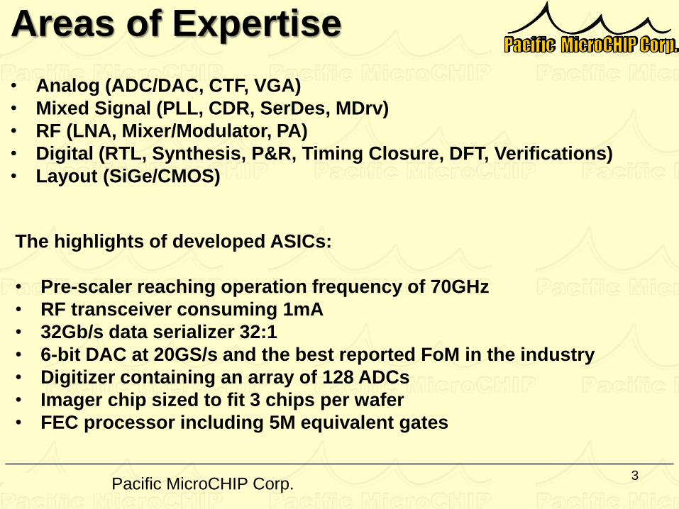
Areas of Expertise
• Analog (ADC/DAC, CTF, VGA)
• Mixed Signal (PLL, CDR, SerDes, MDrv)
• RF (LNA, Mixer/Modulator, PA)
• Digital (RTL, Synthesis, P&R, Timing Closure, DFT, Verifications)
• Layout (SiGe/CMOS)
The highlights of developed ASICs:
• Pre-scaler reaching operation frequency of 70GHz
• RF transceiver consuming 1mA
• 32Gb/s data serializer 32:1
• 6-bit DAC at 20GS/s and the best reported FoM in the industry
• Digitizer containing an array of 128 ADCs
• Imager chip sized to fit 3 chips per wafer
• FEC processor including 5M equivalent gates
Confidential - Pacific MicroCHIP Corp.
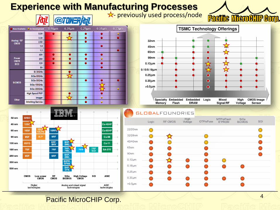
Experience with Manufacturing Processes
4
- previously used process/node
Confidential - Pacific MicroCHIP Corp.
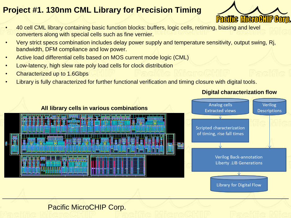
Project #1. 130nm CML Library for Precision Timing
• 40 cell CML library containing basic function blocks: buffers, logic cells, retiming, biasing and level
converters along with special cells such as fine vernier.
• Very strict specs combination includes delay power supply and temperature sensitivity, output swing, Rj,
bandwidth, DFM compliance and low power.
• Active load differential cells based on MOS current mode logic (CML)
• Low-latency, high slew rate poly load cells for clock distribution
• Characterized up to 1.6Gbps
• Library is fully characterized for further functional verification and timing closure with digital tools.
All library cells in various combinations
Digital characterization flow
Confidential - Pacific MicroCHIP Corp.
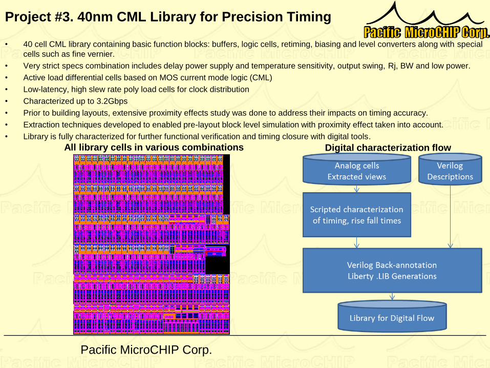
Project #3. 40nm CML Library for Precision Timing
• 40 cell CML library containing basic function blocks: buffers, logic cells, retiming, biasing and level converters along with special
cells such as fine vernier.
• Very strict specs combination includes delay power supply and temperature sensitivity, output swing, Rj, BW and low power.
• Active load differential cells based on MOS current mode logic (CML)
• Low-latency, high slew rate poly load cells for clock distribution
• Characterized up to 3.2Gbps
• Prior to building layouts, extensive proximity effects study was done to address their impacts on timing accuracy.
• Extraction techniques developed to enabled pre-layout block level simulation with proximity effect taken into account.
• Library is fully characterized for further functional verification and timing closure with digital tools.
All library cells in various combinations Digital characterization flow
Confidential - Pacific MicroCHIP Corp.
Commercial ASIC Examples
7
Confidential - Pacific MicroCHIP Corp. 8
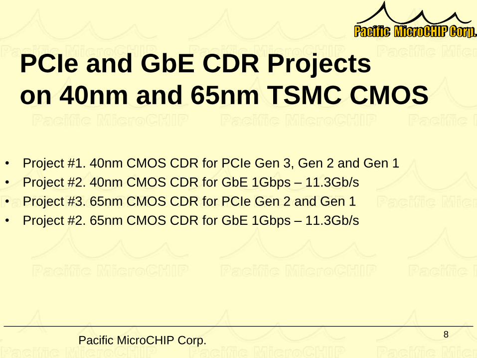
• Project #1. 40nm CMOS CDR for PCIe Gen 3, Gen 2 and Gen 1
• Project #2. 40nm CMOS CDR for GbE 1Gbps – 11.3Gb/s
• Project #3. 65nm CMOS CDR for PCIe Gen 2 and Gen 1
• Project #2. 65nm CMOS CDR for GbE 1Gbps – 11.3Gb/s
PCIe and GbE CDR Projects
on 40nm and 65nm TSMC CMOS
Confidential - Pacific MicroCHIP Corp. 9
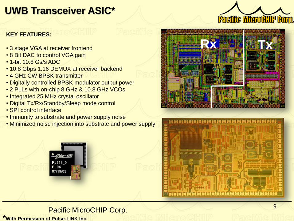
UWB Transceiver ASIC*
Rx Tx
*With Permission of Pulse-LINK Inc.
KEY FEATURES:
• 3 stage VGA at receiver frontend
• 8 Bit DAC to control VGA gain
• 1-bit 10.8 Gs/s ADC
• 10.8 Gbps 1:16 DEMUX at receiver backend
• 4 GHz CW BPSK transmitter
• Digitally controlled BPSK modulator output power
• 2 PLLs with on-chip 8 GHz & 10.8 GHz VCOs
• Integrated 25 MHz crystal oscillator
• Digital Tx/Rx/Standby/Sleep mode control
• SPI control interface
• Immunity to substrate and power supply noise
• Minimized noise injection into substrate and power supply
Confidential - Pacific MicroCHIP Corp. 10
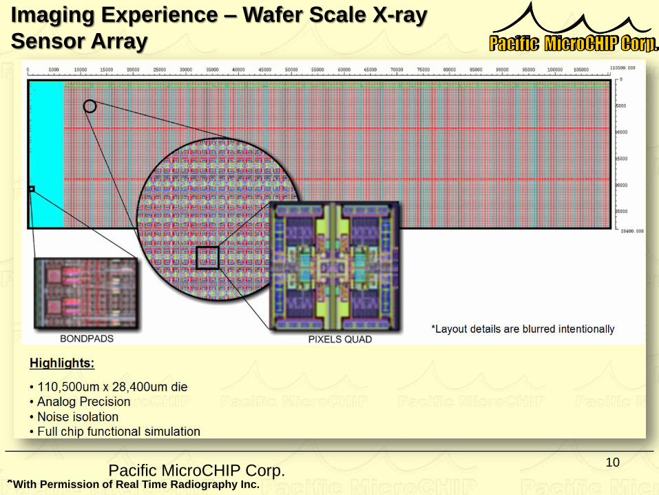
Imaging Experience – Wafer Scale X-ray
Sensor Array
*With Permission of Real Time Radiography Inc.
Confidential - Pacific MicroCHIP Corp.
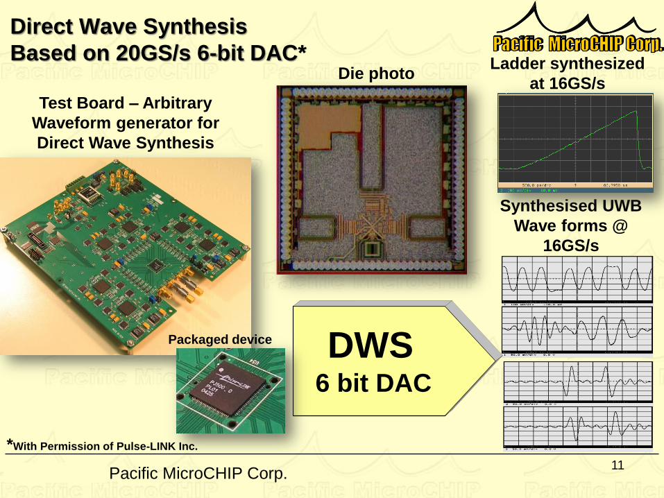
Direct Wave Synthesis
Based on 20GS/s 6-bit DAC*
11
Synthesised UWB
Wave forms @
16GS/s
DWS 6 bit DAC
Ladder synthesized
at 16GS/s
Test Board – Arbitrary
Waveform generator for
Direct Wave Synthesis
Die photo
Packaged device
*With Permission of Pulse-LINK Inc.
Confidential - Pacific MicroCHIP Corp. 12
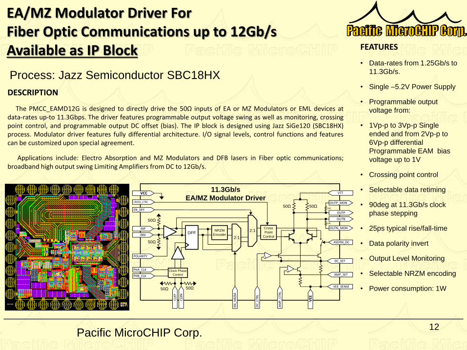
EA/MZ Modulator Driver For Fiber Optic Communications up to 12Gb/s Available as IP Block
Process: Jazz Semiconductor SBC18HX
DESCRIPTION
The PMCC_EAMD12G is designed to directly drive the 50Ω inputs of EA or MZ Modulators or EML devices at data-rates up-to 11.3Gbps. The driver features programmable output voltage swing as well as monitoring, crossing point control, and programmable output DC offset (bias). The IP block is designed using Jazz SiGe120 (SBC18HX) process. Modulator driver features fully differential architecture. I/O signal levels, control functions and features can be customized upon special agreement.
Applications include: Electro Absorption and MZ Modulators and DFB lasers in Fiber optic communications; broadband high output swing Limiting Amplifiers from DC to 12Gb/s.
FEATURES
• Data-rates from 1.25Gb/s to
11.3Gb/s.
• Single –5.2V Power Supply
• Programmable output
voltage from:
• 1Vp-p to 3Vp-p Single
ended and from 2Vp-p to
6Vp-p differential
Programmable EAM bias
voltage up to 1V
• Crossing point control
• Selectable data retiming
• 90deg at 11.3Gb/s clock
phase stepping
• 25ps typical rise/fall-time
• Data polarity invert
• Output Level Monitoring
• Selectable NRZM encoding
• Power consumption: 1W
OUTP
OUTN
11.3Gb/s
EA/MZ Modulator Driver
INNEN
_NR
ZM
INP
CLK
N
CLK
P
Clock Phase
Control
DFF
EN_DFF
PHA_CLK
PHB_CLK AMP_SET
OUTP_MON
OUTN_MON
10K
10K
ASSYM_DC
VEE
VCC
POLARITY
NRZM
Encoder2:1
2:1
DC_SET
VTT
50Ω
VEE_SENSE
Cross
Point
Control
CROSS_CTRL
50Ω
50Ω
50Ω
50Ω 50Ω
AM
P_C
TRL
DC
_CTR
L
Confidential - Pacific MicroCHIP Corp.
SBIR Funded ASICs
13
Confidential - Pacific MicroCHIP Corp.
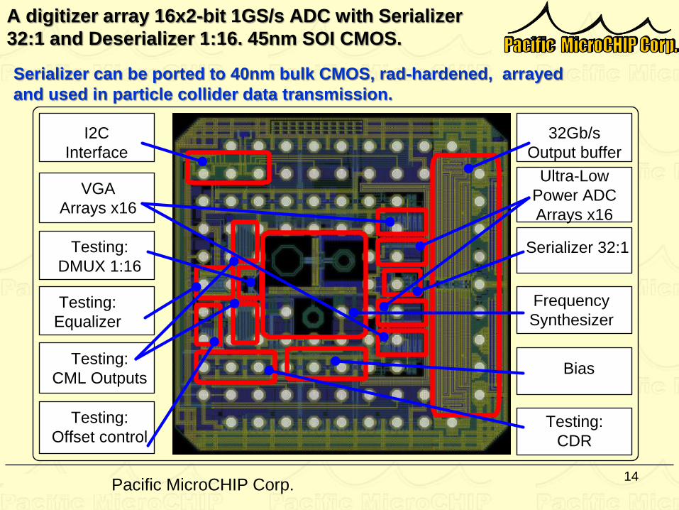
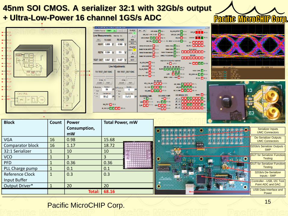
A digitizer array 16x2-bit 1GS/s ADC with Serializer
32:1 and Deserializer 1:16. 45nm SOI CMOS.
14
I2C
Interface
32Gb/s
Output buffer
VGA
Arrays x16
Ultra-Low
Power ADC
Arrays x16
Testing:
DMUX 1:16
Testing:
Equalizer
Serializer 32:1
Testing:
CDR
Frequency
Synthesizer
BiasTesting:
CML Outputs
Testing:
Offset control
Serializer can be ported to 40nm bulk CMOS, rad-hardened, arrayed
and used in particle collider data transmission.
Confidential - Pacific MicroCHIP Corp.
Block Count Power Consumption, mW
Total Power, mW
VGA 16 0.98 15.68 Comparator block 16 1.17 18.72 32:1 Serializer 1 10 10 VCO 1 3 3 PFD 1 0.36 0.36 PLL Charge pump 1 0.1 0.1 Reference Clock Input Buffer
1 0.3 0.3
Output Driver* 1 20 20 Total: 68.16
45nm SOI CMOS. A serializer 32:1 with 32Gb/s output
+ Ultra-Low-Power 16 channel 1GS/s ADC
15
DUT for Serializer Function
Testing
DUT for Serializer Function
Testing
De-Serializer Outputs
UMC Connectors
Serializer Inputs
UMC Connectors
32Gb/s De-Serializer
Inputs - SMP
Controller - USB, I2C Test
Point ADC and DAC
32Gb/s Serializer Outputs -
SMP
USB Data Interface and
Power
Confidential - Pacific MicroCHIP Corp.
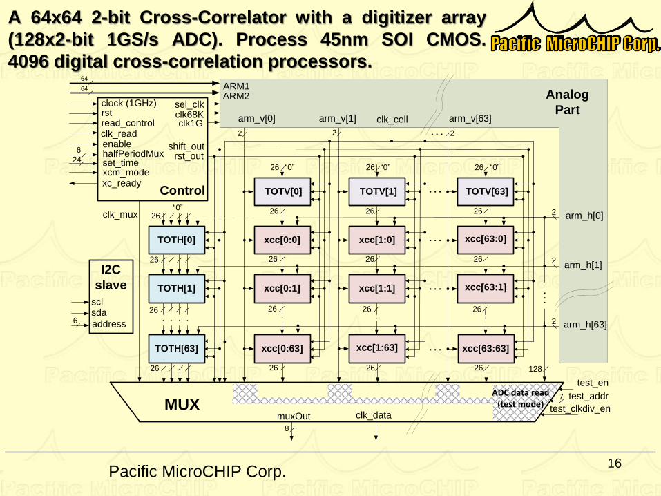
A 64x64 2-bit Cross-Correlator with a digitizer array
(128x2-bit 1GS/s ADC). Process 45nm SOI CMOS.
4096 digital cross-correlation processors.
16
2
MUX
xcc[0:63]
xcc[0:1]
xcc[0:0]
xcc[1:63]
xcc[1:1]
xcc[1:0]
xcc[63:63]
xcc[63:1]
xcc[63:0]
TOTH[63]
TOTH[1]
TOTH[0]
26
. . .
26“0”
Control
2 2
2
rst_outshift_out
rstclock (1GHz)
clk_mux
xcm_modeset_time24
xc_ready
clk_readread_control
muxOut
8
clk_data
enablehalfPeriodMux6
TOTV[0]
64
64
7 test_addr
test_en
test_clkdiv_en
TOTV[1] TOTV[63]
arm_v[63]arm_v[1]arm_v[0]
26
sel_clkclk68Kclk1G
26 “0”
clk_cell
26
2
26 “0” 26 “0”
26 26
26 26
. . .
. . .
. . .
26
. . . .
26 26 26. . .
2
arm_h[0]
arm_h[63]
arm_h[1]
ARM1ARM2
26 26 2626
. . .
. . .
Analog
Part
128
ADC data read(test mode)
I2C
slave
sclsda
address6
Confidential - Pacific MicroCHIP Corp.
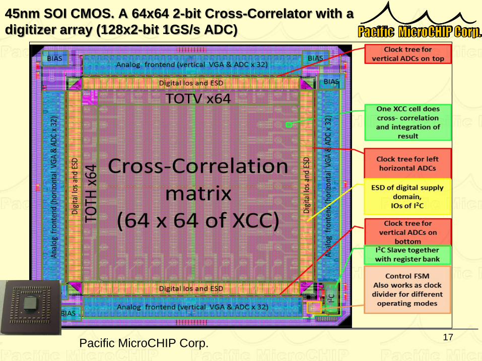
45nm SOI CMOS. A 64x64 2-bit Cross-Correlator with a
digitizer array (128x2-bit 1GS/s ADC)
17
Confidential - Pacific MicroCHIP Corp.
IP Blocks
18
Confidential - Pacific MicroCHIP Corp.
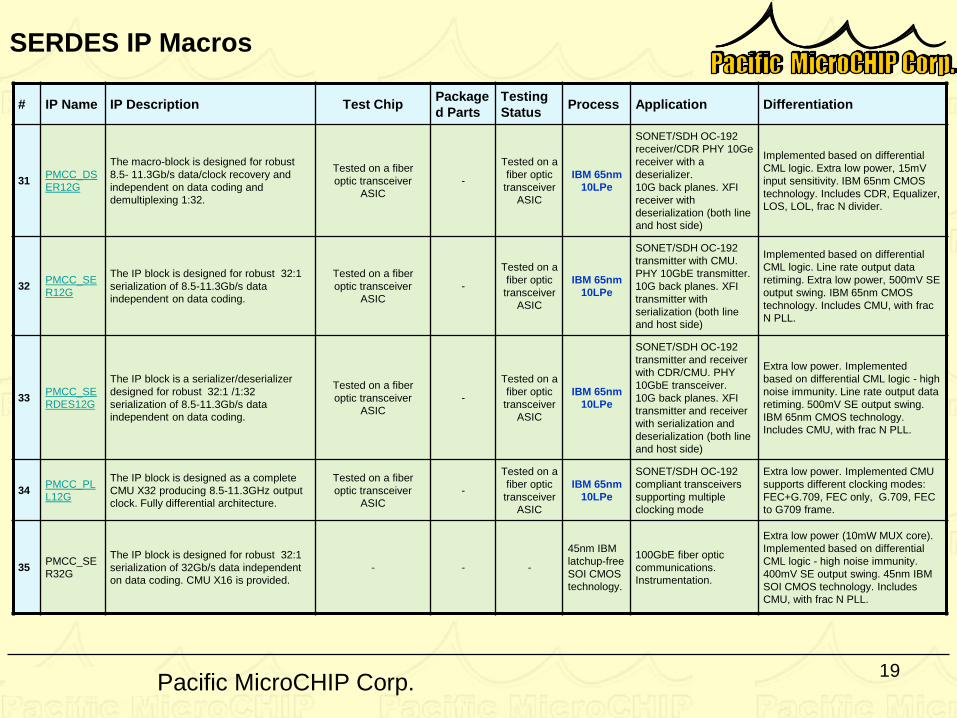
SERDES IP Macros
19
# IP Name IP Description Test Chip Package
d Parts
Testing
Status Process Application Differentiation
31 PMCC_DS
ER12G
The macro-block is designed for robust
8.5- 11.3Gb/s data/clock recovery and
independent on data coding and
demultiplexing 1:32.
Tested on a fiber
optic transceiver
ASIC
-
Tested on a
fiber optic
transceiver
ASIC
IBM 65nm
10LPe
SONET/SDH OC-192
receiver/CDR PHY 10Ge
receiver with a
deserializer.
10G back planes. XFI
receiver with
deserialization (both line
and host side)
Implemented based on differential
CML logic. Extra low power, 15mV
input sensitivity. IBM 65nm CMOS
technology. Includes CDR, Equalizer,
LOS, LOL, frac N divider.
32 PMCC_SE
R12G
The IP block is designed for robust 32:1
serialization of 8.5-11.3Gb/s data
independent on data coding.
Tested on a fiber
optic transceiver
ASIC
-
Tested on a
fiber optic
transceiver
ASIC
IBM 65nm
10LPe
SONET/SDH OC-192
transmitter with CMU.
PHY 10GbE transmitter.
10G back planes. XFI
transmitter with
serialization (both line
and host side)
Implemented based on differential
CML logic. Line rate output data
retiming. Extra low power, 500mV SE
output swing. IBM 65nm CMOS
technology. Includes CMU, with frac
N PLL.
33 PMCC_SE
RDES12G
The IP block is a serializer/deserializer
designed for robust 32:1 /1:32
serialization of 8.5-11.3Gb/s data
independent on data coding.
Tested on a fiber
optic transceiver
ASIC
-
Tested on a
fiber optic
transceiver
ASIC
IBM 65nm
10LPe
SONET/SDH OC-192
transmitter and receiver
with CDR/CMU. PHY
10GbE transceiver.
10G back planes. XFI
transmitter and receiver
with serialization and
deserialization (both line
and host side)
Extra low power. Implemented
based on differential CML logic - high
noise immunity. Line rate output data
retiming. 500mV SE output swing.
IBM 65nm CMOS technology.
Includes CMU, with frac N PLL.
34 PMCC_PL
L12G
The IP block is designed as a complete
CMU X32 producing 8.5-11.3GHz output
clock. Fully differential architecture.
Tested on a fiber
optic transceiver
ASIC
-
Tested on a
fiber optic
transceiver
ASIC
IBM 65nm
10LPe
SONET/SDH OC-192
compliant transceivers
supporting multiple
clocking mode
Extra low power. Implemented CMU
supports different clocking modes:
FEC+G.709, FEC only, G.709, FEC
to G709 frame.
35 PMCC_SE
R32G
The IP block is designed for robust 32:1
serialization of 32Gb/s data independent
on data coding. CMU X16 is provided.
- - -
45nm IBM
latchup-free
SOI CMOS
technology.
100GbE fiber optic
communications.
Instrumentation.
Extra low power (10mW MUX core).
Implemented based on differential
CML logic - high noise immunity.
400mV SE output swing. 45nm IBM
SOI CMOS technology. Includes
CMU, with frac N PLL.
Confidential - Pacific MicroCHIP Corp.
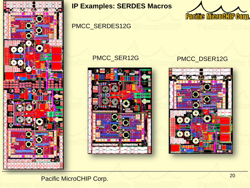
IP Examples: SERDES Macros
20
PMCC_SER12G
PMCC_SERDES12G
PMCC_DSER12G
Confidential - Pacific MicroCHIP Corp. 21
Digital Design Experience
RTL Design
Synthesis (including SRAM)
Place & Route
Static Timing Analysis
Power Analysis
Equivalency Check
Functionality Verification
Confidential - Pacific MicroCHIP Corp. 22
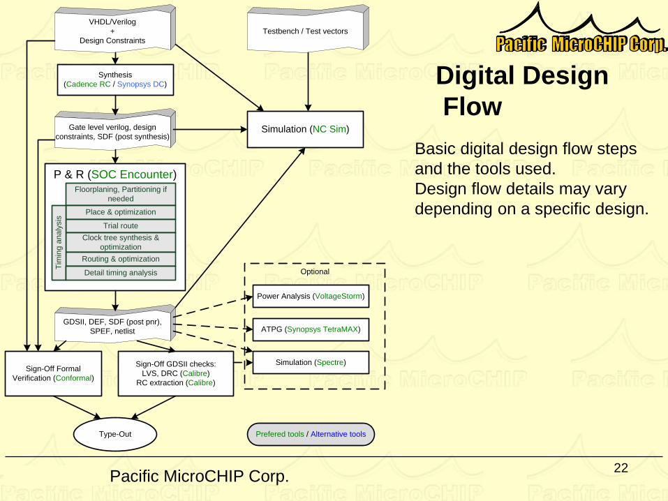
Digital Design
Flow
Basic digital design flow steps
and the tools used.
Design flow details may vary
depending on a specific design.
Optional
VHDL/Verilog
+
Design Constraints
Synthesis
(Cadence RC / Synopsys DC)
Sign-Off Formal
Verification (Conformal)
Gate level verilog, design
constraints, SDF (post synthesis)
P & R (SOC Encounter)Floorplaning, Partitioning if
needed
Place & optimization
Trial route
Clock tree synthesis &
optimization
Routing & optimization
Tim
ing
an
aly
sis
Detail timing analysis
GDSII, DEF, SDF (post pnr),
SPEF, netlist
Power Analysis (VoltageStorm)
Simulation (Spectre)
ATPG (Synopsys TetraMAX)
Sign-Off GDSII checks:
LVS, DRC (Calibre)
RC extraction (Calibre)
Testbench / Test vectors
Type-Out
Simulation (NC Sim)
Prefered tools / Alternative tools
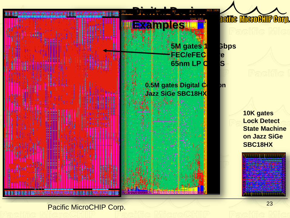
Confidential - Pacific MicroCHIP Corp. 23
0.5M gates Digital Core on
Jazz SiGe SBC18HX
10K gates
Lock Detect
State Machine
on Jazz SiGe
SBC18HX
Digital Design
Examples
5M gates 11.3Gbps
FEC/eFEC Core
65nm LP CMOS
Confidential - Pacific MicroCHIP Corp.
Potential Proposals for DoE
SBIR Program
24
Confidential - Pacific MicroCHIP Corp. 25
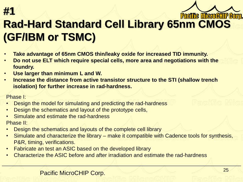
#1
Rad-Hard Standard Cell Library 65nm CMOS
(GF/IBM or TSMC)
• Take advantage of 65nm CMOS thin/leaky oxide for increased TID immunity.
• Do not use ELT which require special cells, more area and negotiations with the
foundry.
• Use larger than minimum L and W.
• Increase the distance from active transistor structure to the STI (shallow trench
isolation) for further increase in rad-hardness.
Phase I:
• Design the model for simulating and predicting the rad-hardness
• Design the schematics and layout of the prototype cells,
• Simulate and estimate the rad-hardness
Phase II:
• Design the schematics and layouts of the complete cell library
• Simulate and characterize the library – make it compatible with Cadence tools for synthesis,
P&R, timing, verifications.
• Fabricate an test an ASIC based on the developed library
• Characterize the ASIC before and after irradiation and estimate the rad-hardness
Confidential - Pacific MicroCHIP Corp. 26
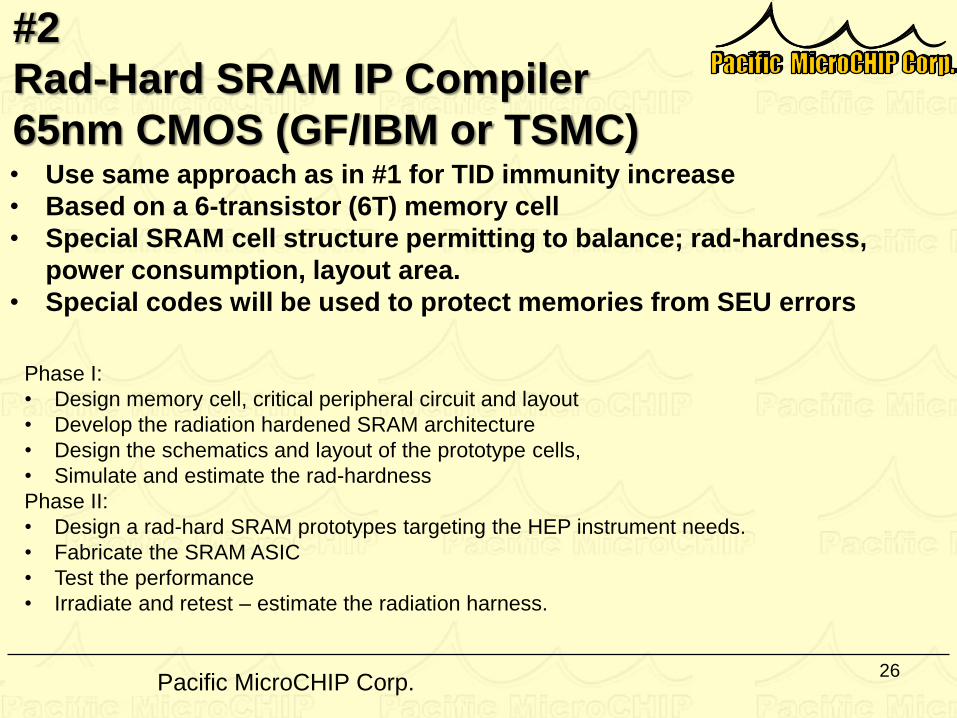
#2
Rad-Hard SRAM IP Compiler
65nm CMOS (GF/IBM or TSMC) • Use same approach as in #1 for TID immunity increase
• Based on a 6-transistor (6T) memory cell
• Special SRAM cell structure permitting to balance; rad-hardness,
power consumption, layout area.
• Special codes will be used to protect memories from SEU errors
Phase I:
• Design memory cell, critical peripheral circuit and layout
• Develop the radiation hardened SRAM architecture
• Design the schematics and layout of the prototype cells,
• Simulate and estimate the rad-hardness
Phase II:
• Design a rad-hard SRAM prototypes targeting the HEP instrument needs.
• Fabricate the SRAM ASIC
• Test the performance
• Irradiate and retest – estimate the radiation harness.
Confidential - Pacific MicroCHIP Corp. 27
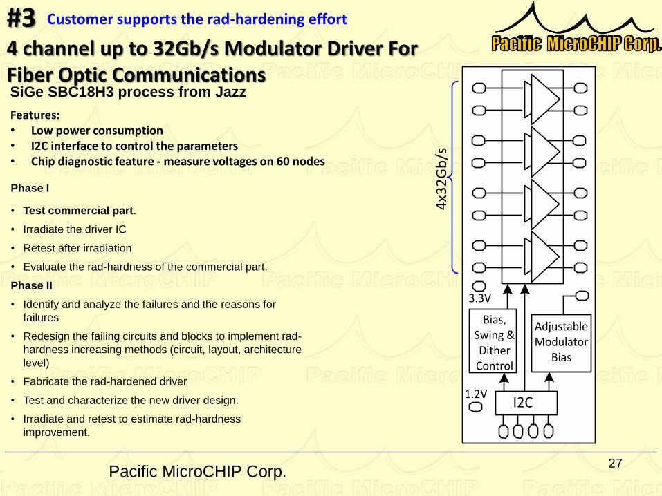
#3 4 channel up to 32Gb/s Modulator Driver For Fiber Optic Communications SiGe SBC18H3 process from Jazz
Phase I
• Test commercial part.
• Irradiate the driver IC
• Retest after irradiation
• Evaluate the rad-hardness of the commercial part.
Phase II
• Identify and analyze the failures and the reasons for
failures
• Redesign the failing circuits and blocks to implement rad-
hardness increasing methods (circuit, layout, architecture
level)
• Fabricate the rad-hardened driver
• Test and characterize the new driver design.
• Irradiate and retest to estimate rad-hardness
improvement.
I2C
Bias, Swing &Dither
Control
Adjustable Modulator
Bias
1.2V
3.3V
4x3
2G
b/s
Customer supports the rad-hardening effort
Features: • Low power consumption • I2C interface to control the parameters • Chip diagnostic feature - measure voltages on 60 nodes
Confidential - Pacific MicroCHIP Corp. 28
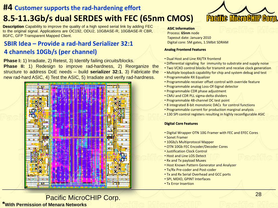
Description Capability to improve the quality of a high speed serial link by adding FEC
to the original signal. Applications are OC192, ODU2, 10GBASE-R, 10GBASE-R CBR,
8GFC, GFP Transparent Mapped Client.
Analog Frontend Features • Dual Host and Line RX/TX frontend • Differential signaling for immunity to substrate and supply noise • Two VCXO control blocks for transmit and receive clock generation • Multiple loopback capability for chip and system debug and test • Programmable RX Equalizer • Programmable receiver offset control with override feature • Programmable analog Loss-Of-Signal detector • Programmable CDR phase adjustment • CMU and CDR PLL sigma-delta dividers • Programmable 48-channel DC test point • 8 integrated 8-bit monotonic DACs for control functions • Programmable current for production marginal analysis • 130 SPI control registers resulting in highly reconfigurable ASIC Digital Core Features • Digital Wrapper OTN 10G Framer with FEC and EFEC Cores • Sonet Framer • 10Gb/s Multiprotocol Mapper • OTN 10Gb FEC Encoder/Decoder Cores • Justification Clock Control • Host and Line LOS Detect • Rx and Tx payload Muxes • Host Known Pattern Generator and Analyzer • Tx/Rx Pre-coder and Post-coder • Tx and Rx Serial Overhead and GCC ports • SPI, MDIO, GPINT Interfaces • Tx Error Insertion
ASIC Information Process: 65nm node Tapeout date: January 2010 Digital core: 5M gates, 1.5Mbit SDRAM
*With Permission of Menara Networks
#4 Customer supports the rad-hardening effort
8.5-11.3Gb/s dual SERDES with FEC (65nm CMOS)
Phase I: 1) Irradiate, 2) Retest, 3) Identify failing circuits/blocks.
Phase II: 1) Redesign to improve rad-hardness, 2) Reorganize the
structure to address DoE needs – build serializer 32:1, 3) Fabricate the
new rad-hard ASIC, 4) Test the ASIC, 5) Irradiate and verify rad-hardness.
SBIR Idea – Provide a rad-hard Serializer 32:1
4 channels 10Gb/s (per channel)
Confidential - Pacific MicroCHIP Corp. 29
#5 Low-Power/Short-Range Transceiver
Rx:
Fc= 13.56MHz,
Pin= -100dBm
Iee=2mA
Tx:
Fc=433.8MHz,
Data rate 13.5 Mbps,
Iee=1mA
Project goal – provide a rad-hard low power wireless transceiver for diagnostic and command data transmission to/from inside of highly packed detectors
Phase I: 1) Design critical blocks on 65nm CMOS in order to increase the radiation hardness. Implement
other hardening means such as increase minimum channel W and L, increase active area distance to the
STI.
Phase II: 1) Integrate the transceiver with BB block, 2) Fabricate the rad-hard transceiver, 3) Test the ASIC,
4) Irradiate and verify rad-hardness, 5) Produce the complete transceiver module ready for application inside
particle detectors.

Confidential - Pacific MicroCHIP Corp.
Suggestions, Comments, Any
Feed-Back is Greatly Appreciated !
Thank You
30