Embed Size (px)
Citation preview
– 3 – 60050-521 CEI:2002
3 Termes et définitions
3 Terms and definitions
PARTIE 521 : DISPOSITIFS À SEMICONDUCTEURSET CIRCUITS INTÉGRÉS
PART 521: SEMICONDUCTOR DEVICESAND INTEGRATED CIRCUITS
Section 521-01 – Notions de physique atomiqueSection 521-01 – Introduction to atomic physics
521-01-01système non quantifié (de particules), m
système de particules dont on suppose que les énergies sont susceptibles de varier demanière continue. Le nombre des états microscopiques, défini par les positions et les vitessesdes particules à un instant donné, est alors non limité
non-quantized system (of particles)
system of particles whose energies are assumed to be capable of varying in a continuousmanner and in which the number of microscopic states defined by the positions and velocitiesof the particles at a given instant is therefore unlimited
cn 非量子化系统非量子化系统非量子化系统非量子化系统(粒子的)de nichtquantisiertes System (von Teilchen), nes sistema no cualificado (de partículas)ja (粒子の)非量子化系(粒子の)非量子化系(粒子の)非量子化系(粒子の)非量子化系pl układ niekwantowany (cząstek)pt sistema não quantificado (de partículas)sv okvantiserat system
521-01-02système quantifié (de particules), m
système de particules dont les énergies ne peuvent prendre que des valeurs discrètes
quantized system (of particles)
system of particles the energies of which can have discrete values only
cn 量子化系统量子化系统量子化系统量子化系统(粒子的)de quantisiertes System (von Teilchen), nes sistema cuantificado (de partículas)ja (粒子の)量子化系(粒子の)量子化系(粒子の)量子化系(粒子の)量子化系pl układ kwantowany (cząstek)pt sistema quantificado (de partículas)sv kvantiserat system
60050-521 IEC:2002 – 4 –
521-01-03statistique de Maxwell-Boltzmann, f
ensemble de probabilités des états macroscopiques d'un système non quantifié de particulesdéterminé par les valeurs moyennes des coordonnées de positions, des vitesses ou del'énergie, dans un volume très petit, mais non nul du système
Maxwell-Boltzmann statisticsprobability distribution of the macroscopic states of a non-quantized system of particles,defined by the average values of the position, velocity or energy co-ordinates, in a very small,but finite, volume of the system
cn 麦克斯韦麦克斯韦麦克斯韦麦克斯韦----玻尔兹曼统计玻尔兹曼统计玻尔兹曼统计玻尔兹曼统计de Maxwell-Boltzmann-Statistik, fes estadística de Maxwell-Boltzmannja マックスウェル‐ボルツマン統計マックスウェル‐ボルツマン統計マックスウェル‐ボルツマン統計マックスウェル‐ボルツマン統計pl rozkład Maxwella-Boltzmannapt estatística de Maxwell-Boltzmannsv Maxwell-Boltzmann-fördelning
521-01-04relation de Boltzmann, f
relation exprimant que, à une constante additive près, l'entropie d'un système de particulesest égale au produit du logarithme népérien de la probabilité de son état macroscopique parla constante de Boltzmann
Boltzmann relationequation stating that, apart from an additive constant, the entropy of a system of particles isequal to the product of the Napierian (natural) logarithm of the probability of its macroscopicstate and the Boltzmann constant
cn 玻尔兹曼关系玻尔兹曼关系玻尔兹曼关系玻尔兹曼关系de Boltzmann-Beziehung, fes relación de Boltzmannja ボルツマン関係ボルツマン関係ボルツマン関係ボルツマン関係pl zależność Boltzmannapt relação de Boltzmannsv Boltzmanns ekvation
– 5 – 60050-521 CEI:2002
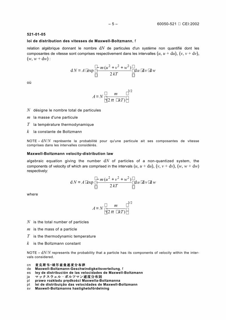
521-01-05loi de distribution des vitesses de Maxwell-Boltzmann, f
relation algébrique donnant le nombre dN de particules d'un système non quantifié dont lescomposantes de vitesse sont comprises respectivement dans les intervalles (u, u + du), (v, v + dv),(w, w + dw) :
wvukT
wvumAN d d d 2
) ( exp d222
⋅⋅
++−⋅=
où
) (2
3/2
⋅
=kT
mNAπ
N désigne le nombre total de particules
m la masse d'une particule
T la température thermodynamique
k la constante de Boltzmann
NOTE – dN/N représente la probabilité pour qu'une particule ait ses composantes de vitessecomprises dans les intervalles considérés.
Maxwell-Boltzmann velocity-distribution law
algebraic equation giving the number dN of particles of a non-quantized system, thecomponents of velocity of which are comprised in the intervals (u, u + du), (v, v + dv), (w, w + dw)respectively:
wvukT
wvumAN d d d 2
) ( exp d222
⋅⋅
++−⋅=
where
) (2
3/2
⋅
=kT
mNAπ
N is the total number of particles
m is the mass of a particle
T is the thermodynamic temperature
k is the Boltzmann constant
NOTE – dN/N represents the probability that a particle has its components of velocity within the inter-vals considered.
cn 麦克斯韦麦克斯韦麦克斯韦麦克斯韦----玻尔兹曼速度分布律玻尔兹曼速度分布律玻尔兹曼速度分布律玻尔兹曼速度分布律de Maxwell-Boltzmann-Geschwindigkeitsverteilung, fes ley de distribución de las velocidades de Maxwell-Boltzmannja マックスウェル‐ボルツマン速度分布則マックスウェル‐ボルツマン速度分布則マックスウェル‐ボルツマン速度分布則マックスウェル‐ボルツマン速度分布則pl prawo rozkładu prędkości Maxwella-Boltzmannapt lei de distribuição das velocidades de Maxwell-Boltzmannsv Maxwell-Boltzmanns hastighetsfördelning
60050-521 IEC:2002 – 6 –
521-01-06atome de Bohr, m
modèle de l'atome fondé sur les conceptions de Bohr et de Sommerfeld, d'après lesquellesles électrons d'un atome décriraient autour du noyau des orbites circulaires ou elliptiquesdiscrètesNOTE – A chacun des degrés de liberté de l'atome correspond une série d'états énergétiques quidéterminent les séries spectrales susceptibles d'être émises par l'atome.
Bohr atommodel of the atom based on the conception of Bohr and Sommerfeld, according to which theelectrons of an atom move around the nucleus in discrete circular or elliptical orbitsNOTE – To each of the degrees of freedom of the atom there corresponds a series of energy stateswhich determine the spectral series that may be emitted by the atom.
cn 玻尔原子玻尔原子玻尔原子玻尔原子de Bohr-Atommodell, nes átomo de Bohrja ボーア原子ボーア原子ボーア原子ボーア原子pl atom Bohrapt átomo de Bohrsv Bohrs atommodell
521-01-07nombre quantique (d'un électron dans un atome donné), m
chacun des nombres caractérisant les degrés de liberté d'un électron dans un atome donné :
– le nombre quantique principal n– le nombre quantique secondaire l– le nombre quantique de spin s– le nombre quantique interne j
quantum number (of an electron in a given atom)
each of the numbers characterizing the degree of freedom of an electron in a given atom:
– the principal quantum number n– the orbital quantum number l– the spin quantum number s– the total angular momentum quantum number j
cn 量子数量子数量子数量子数(给定原子中电子的)de Quantenzahl (eines Elektrons in einem gegebenen Atom), fes número cuántico (de un electrón de un átomo dado)ja (与えられた原子内の電子の)量子数(与えられた原子内の電子の)量子数(与えられた原子内の電子の)量子数(与えられた原子内の電子の)量子数pl liczba kwantowa (elektronu w danym atomie)pt número quântico (de um electrão num átomo dado)sv kvanttal
– 7 – 60050-521 CEI:2002
521-01-08
symb. : nnombre quantique principal, mnombre quantique entier positif qui caractérise les variations importantes du niveau d'énergiedes électrons dans un atomeNOTE – Selon le modèle de l'atome de Bohr, le nombre quantique principal peut être considéré commecaractérisant le grandeur de l'orbite d'un électron.
principal quantum numberfirst quantum numberpositive integer number characterizing the important changes of energy level of the electronsin an atomNOTE – According to the Bohr atom model, the main quantum number may be considered ascharacterizing the size of an electron orbit.
cn 主量子数主量子数主量子数主量子数de Hauptquantenzahl, fes número cuántico principalja 主量子数;第主量子数;第主量子数;第主量子数;第1量子数量子数量子数量子数pl liczba kwantowa główna; liczba kwantowa pierwszapt número quântico principalsv huvudkvanttal
521-01-09
symb. : lnombre quantique secondaire, mnombre quantique orbital, m
nombre quantique qui peut prendre toutes les valeurs entières de zéro à n–1, n désignant lenombre quantique principalNOTE – Selon le modèle de l'atome de Bohr, le nombre quantique secondaire peut être considérécomme caractérisant le moment cinétique de l'électron dans son mouvement orbital.
orbital quantum numbersecond quantum number
quantum number which can have all whole values from zero to n–1, n designating the mainquantum numberNOTE – According to the Bohr atom model, the orbital quantum number may be considered ascharacterizing the angular momentum of the electron in its orbital motion round the nucleus.
cn 轨道量子数轨道量子数轨道量子数轨道量子数de Bahndrehimpulsquantenzahl, fes número cuántico secundarioja 軌道量子数;第軌道量子数;第軌道量子数;第軌道量子数;第2量子数量子数量子数量子数pl liczba kwantowa orbitalna; liczba kwantowa drugapt número quântico orbital; número quântico secundáriosv bikvanttal
60050-521 IEC:2002 – 8 –
521-01-10
symb. : s(nombre quantique de) spin, m
nombre quantique qui caractérise le moment cinétique de l'électron considéré comme unepetite sphère chargée en rotation autour de son axeNOTE – Le spin peut prendre deux valeurs : +1/2 et –1/2.
spin (quantum number)quantum number which gives the angular momentum of the electron considered as a smallcharged sphere revolving rotating around its axisNOTE – The spin may have two values: +1/2 or –1/2.
cn 自旋自旋自旋自旋((((量子数量子数量子数量子数))))de Spinquantenzahl, f; Spin, mes espínja スピン(量子数)スピン(量子数)スピン(量子数)スピン(量子数)pl liczba spinowa; spinpt (número quântico de) spinsv spinnkvanttal
521-01-11
symb. : jnombre quantique interne, m
nombre quantique qui caractérise la résultante des champs magnétiques engendrés parl'électron, d'une part dans son mouvement orbital et d'autre part dans son mouvement de rotation
NOTE – Les valeurs de ce nombre j forment une suite de nombres semi-entiers et entiers.
total angular momentum quantum numberquantum number which gives the resultant of the magnetic field engendered by the electrondue to its orbital movement and due to its revolving on its own axis
NOTE – The values of this number j form a set of integral and semi-integral values.
cn 总角动量量子数总角动量量子数总角动量量子数总角动量量子数de Gesamtdrehimpulsquantenzahl, fes número cuántico internoja 総角運動量量子数総角運動量量子数総角運動量量子数総角運動量量子数pl liczba kwantowa całkowitego momentu kątowegopt (número quântico de) momento angular totalsv kvanttal för totalt rörelsemängdsmoment
521-01-12niveau d'énergie, m
énergie correspondant à un état quantifié d'un système physique
energy level (of a particle)
energy associated with a quantum state of a physical system
cn 能级能级能级能级(粒子的)de Energieniveau (eines Teilchens), nes nivel de energía (de una partícula); nivel energético (de una partícula)ja ((((粒子の)エネルギー準位粒子の)エネルギー準位粒子の)エネルギー準位粒子の)エネルギー準位pl poziom energetyczny (cząstki)pt nível de energiasv energinivå
– 9 – 60050-521 CEI:2002
521-01-13diagramme énergétique, m
diagramme représentant les niveaux d'énergie des particules d'un système quantifié par desdroites horizontales, ayant pour ordonnées l'énergie de ces particules
energy-level diagramdiagram representing the energy levels of the particles of a quantized system by horizontallines, having for ordinates the energy of these particles
cn 能级图能级图能级图能级图de Energieniveau-Diagramm, nes diagrama energéticoja エネルギー準位図エネルギー準位図エネルギー準位図エネルギー準位図pl wykres poziomów energetycznych (cząstek)pt diagrama de níveis de energia; diagrama energéticosv energinivådiagram
521-01-14principe d'exclusion de Pauli-Fermi, mprincipe suivant lequel chaque niveau d'énergie d'un système quantifié ne peut contenir quezéro, une ou deux particulesNOTE – Dans le cas de deux électrons, les spins sont de signes contraires.
Pauli-Fermi exclusion principlePauli principleprinciple stating that each energy level of a quantized system can include only none, one ortwo particlesNOTE – In the case of two electrons, the spins are of opposite sign.
cn 泡利泡利泡利泡利----费米不相容原理;泡利原理费米不相容原理;泡利原理费米不相容原理;泡利原理费米不相容原理;泡利原理de Pauli-Prinzip, nes principio de exclusión de Pauli-Fermija パウリ‐フェルミの排他律;パウリの原理パウリ‐フェルミの排他律;パウリの原理パウリ‐フェルミの排他律;パウリの原理パウリ‐フェルミの排他律;パウリの原理pl zasada Pauliego-Fermiego; zakaz Pauliegopt princípio de exclusão de Pauli-Fermisv Pauli-Fermis princip
521-01-15statistique de Fermi-Dirac, fstatistique de Fermi, fensemble de probabilités des états macroscopiques d'un système quantifié de particules,satisfaisant au principe d'exclusion de Pauli-Fermi
Fermi-Dirac statisticsFermi statisticsset of probabilities of the macroscopic states of a quantized system of particles, with onlydiscrete energy levels, obeying the Pauli-Fermi exclusion principle
cn 费米费米费米费米----狄拉克统计;费米统计狄拉克统计;费米统计狄拉克统计;费米统计狄拉克统计;费米统计de Fermi-Dirac-Statistik, f; Fermi-Statistik, fes estadística de Fermi-Dirac; estadística de Fermija フェルミ‐ディラック統計;フェルミ統計フェルミ‐ディラック統計;フェルミ統計フェルミ‐ディラック統計;フェルミ統計フェルミ‐ディラック統計;フェルミ統計pl rozkład Fermiego-Diracapt estatística de Fermi-Dirac; estatística de Fermisv fermistatistik
60050-521 IEC:2002 – 10 –
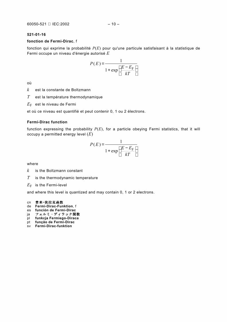
521-01-16fonction de Fermi-Dirac, f
fonction qui exprime la probabilité P(E) pour qu'une particule satisfaisant à la statistique deFermi occupe un niveau d'énergie autorisé E
−+
=
kTE E
EPF exp 1
1 )(
où
k est la constante de Boltzmann
T est la température thermodynamique
EF est le niveau de Fermi
et où ce niveau est quantifié et peut contenir 0, 1 ou 2 électrons.
Fermi-Dirac function
function expressing the probability P(E), for a particle obeying Fermi statistics, that it willoccupy a permitted energy level (E)
−+
=
kTE E
EPF exp 1
1 )(
where
k is the Boltzmann constant
T is the thermodynamic temperature
EF is the Fermi-level
and where this level is quantized and may contain 0, 1 or 2 electrons.
cn 费米费米费米费米----狄拉克函数狄拉克函数狄拉克函数狄拉克函数de Fermi-Dirac-Funktion, fes función de Fermi-Diracja フェルミ‐ディラック関数フェルミ‐ディラック関数フェルミ‐ディラック関数フェルミ‐ディラック関数pl funkcja Fermiego-Diracapt função de Fermi-Diracsv Fermi-Dirac-funktion
– 11 – 60050-521 CEI:2002
521-01-17niveau de Fermi, mdans un solide, niveau d'énergie qui sépare les états occupés des états inoccupés à latempérature de zéro kelvinNOTE – Quand une bande interdite sépare les états occupés des états inoccupés, le niveau de Fermiest assigné au milieu de la bande interdite.
Fermi levelin a solid, energy level separating the occupied states from the unoccupied states at atemperature of zero kelvinNOTE – When a forbidden band separates the occupied and unoccupied states, the Fermi-level isassigned to the centre of the forbidden band.
cn 费米能级费米能级费米能级费米能级de Fermi-Niveau, nes nivel de Fermija フェルミ準位フェルミ準位フェルミ準位フェルミ準位pl poziom Fermiegopt nível de Fermisv ferminivå
521-01-18électron célibataire, m
électron qui se trouve seul sur un niveau d'énergie
lone electronelectron which is alone on an energy level
cn 孤电子孤电子孤电子孤电子de Einzelelektron, nes electrón sueltoja 孤立電子孤立電子孤立電子孤立電子pl elektron samotnypt electrão solitáriosv ensam elektron
60050-521 IEC:2002 – 12 –
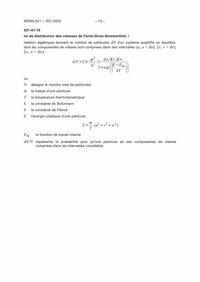
521-01-19loi de distribution des vitesses de Fermi-Dirac-Sommerfeld, f
relation algébrique donnant le nombre de particules dN d'un système quantifié en équilibre,dont les composantes de vitesse sont comprises dans des intervalles (u, u + du), (v, v + dv),(w, w + dw) :
−+
⋅⋅⋅⋅=
kTE Ewvu
hmNN
M3
3
exp 1
d d d 2 d
où
N désigne le nombre total de particules
m la masse d'une particule
T la température thermodynamique
k la constante de Boltzmann
h la constante de Planck
E l'énergie cinétique d'une particule,
) ( 2
222 wvumE ++=
EM la fonction de travail interne
dN/N représente la probabilité pour qu'une particule ait ses composantes de vitessecomprises dans les intervalles considérés.
– 13 – 60050-521 CEI:2002
521-01-19Fermi-Dirac-Sommerfeld velocity distribution law
algebraic equation giving the number dN of particles of a quantized system in equilibrium, thevelocity components of which are included in the intervals (u, u + du), (v, v + dv), (w, w + dw):respectively:
−+
⋅⋅⋅⋅=
kTE Ewvu
hmNN
M3
3
exp 1
d d d 2 d
where
N is the total number of particles
m is the mass of the particle
T is the thermodynamic temperature
k is the Boltzmann constant
h is the Planck constant
E is the kinetic energy of a particle,
) ( 2
222 wvumE ++=
EM is the inner work function
dN/N represents the probability that a particle has its components within the intervalsconsidered.
cn 费米费米费米费米----狄拉克狄拉克狄拉克狄拉克----索末菲速度分布律索末菲速度分布律索末菲速度分布律索末菲速度分布律de Fermi-Dirac-Sommerfeld-Geschwindigkeitsverteilung, fes ley de distribución de las velocidades de Fermi-Dirac-Sommerfeldja フェルミ‐ディラック‐ゾンマーフェルト速度分布則フェルミ‐ディラック‐ゾンマーフェルト速度分布則フェルミ‐ディラック‐ゾンマーフェルト速度分布則フェルミ‐ディラック‐ゾンマーフェルト速度分布則pl prawo rozkładu prędkości Fermiego-Diraca-Sommerfeldapt lei de distribuição das velocidades de Fermi-Dirac-Sommerfeldsv fermifördelning
521-01-20effet photoélectrique, m
phénomène électrique produit par l'absorption de photons
photoelectric effectelectrical phenomena produced by absorption of photons
cn 光电效应光电效应光电效应光电效应de photoelektrischer Effekt, m; Photoeffekt, mes efecto fotoeléctricoja 光電効果光電効果光電効果光電効果pl zjawisko fotoelektrycznept efeito fotoeléctricosv fotoelektrisk effekt
60050-521 IEC:2002 – 14 –
521-01-21effet photovoltaïque, m
effet photoélectrique dans lequel l'absorption de photons produit une force électromotrice
photovoltaic effectphotoelectric effect in which an e.m.f. is produced by the absorption of photons
cn 光生伏打效应;光伏效应光生伏打效应;光伏效应光生伏打效应;光伏效应光生伏打效应;光伏效应de Sperrschicht-Photoeffekt, m; photovoltaischer Effekt, mes efecto fotovoltaicoja 光起電力効果光起電力効果光起電力効果光起電力効果pl zjawisko fotowoltaicznept efeito fotovoltaicosv fotoelektromotorisk effekt
521-01-22effet photoconductif, meffet photoélectrique caractérisé par une variation de conductivité électrique
photoconductive effectphotoelectric effect characterized by the variation of electric conductivity
cn 光电导效应光电导效应光电导效应光电导效应de Photoleiteffekt, mes efecto fotoconductivoja 光導電効果光導電効果光導電効果光導電効果pl zjawisko fotokonduktywnept efeito fotocondutivosv fotokonduktiv effekt
521-01-23effet photoélectromagnétique, m
dans un semiconducteur soumis à un champ magnétique et à un rayonnement électro-magnétique, apparition d'un champ électrique perpendiculaire au champ magnétique et auflux des porteurs de charge engendrés par effet photoélectrique et diffusant dans lesemiconducteur
photoelectromagnetic effectin a semiconductor subjected to a magnetic field and electromagnetic radiation, the develo-pment of an electric field perpendicular to the magnetic field and to the flow of charge carriersgenerated by the photoelectric effect and diffusing in the semiconductor
cn 光磁电效应光磁电效应光磁电效应光磁电效应de photoelektromagnetischer Effekt, mes efecto fotoelectromagnéticoja 光電磁効果光電磁効果光電磁効果光電磁効果pl zjawisko fotomagnetoelektrycznept efeito fotoelectromagnéticosv fotoelektromagnetisk effekt
– 15 – 60050-521 CEI:2002
Section 521-02 – Propriétés des matériaux semiconducteursSection 521-02 – Properties of semiconductor materials
521-02-01semiconducteur, m
substance dont la conductivité totale due aux porteurs de charge des deux signes estnormalement comprise entre celle des conducteurs et celle des isolants, et dont la densitédes porteurs de charge peut être modifiée par des excitations extérieures
semiconductorsubstance whose total conductivity due to charge carriers of both signs is normally in therange between that of conductors and insulants, and in which the charge carrier density canbe changed by external means
cn 半导体半导体半导体半导体de Halbleiter, mes semiconductorja 半導体半導体半導体半導体pl półprzewodnikpt semicondutorsv halvledare
521-02-02semiconducteur élémentaire, m
semiconducteur constitué à l'état pur d'un seul élément
single-element semiconductorsemiconductor which in the pure state consists of a single element
cn 单元素半导体单元素半导体单元素半导体单元素半导体de Einzelelement-Halbleiter, mes semiconductor elementalja 単元素半導体単元素半導体単元素半導体単元素半導体pl półprzewodnik pierwiastkowypt semicondutor elementarsv ettelementshalvledare
521-02-03semiconducteur composé, m
semiconducteur constitué à l'état pur de plusieurs éléments dans des proportions proches deleur composition stoechiométrique
compound semiconductorsemiconductor which in the pure state consists of several elements in proportions close to thestochiometric composition
cn 化合物半导体化合物半导体化合物半导体化合物半导体de Verbindungshalbleiter, mes semiconductor compuestoja 化合物半導体化合物半導体化合物半導体化合物半導体pl półprzewodnik złożonypt semicondutor compostosv sammansatt halvledare
60050-521 IEC:2002 – 16 –
521-02-04impureté, f
atomes étrangers dans un semiconducteur élémentaireatomes étrangers ou atomes en excédent ou déficit par rapport à la composition stoechio-métrique d'un semiconducteur composé
impurityforeign atoms in a single-element semiconductorforeign atoms or either an excess or a deficiency of atoms with respect to the stochiometriccomposition of a compound semiconductor
cn 杂质杂质杂质杂质de Störstelle, fes impurezasja 不純物不純物不純物不純物pl domieszka; zanieczyszczeniept impurezasv störämne
521-02-05énergie d'activation des impuretés, f
écart entre un niveau d'énergie intermédiaire dû à une impureté et la bande énergétiquevoisine
impurity activation energygap between an intermediate energy level due to an impurity and the adjacent energy band
cn 杂质激活能杂质激活能杂质激活能杂质激活能de Störstellen-Aktivierungsenergie, fes energía de activación de impurezasja 不純物活性化エネルギー不純物活性化エネルギー不純物活性化エネルギー不純物活性化エネルギーpl energia aktywacji domieszekpt energia de activação das impurezassv aktiveringsenergi för störatom
521-02-06semiconducteur ionique, m
semiconducteur dans lequel la conductivité électrique due au mouvement des ions estprédominante par rapport à celle due au mouvement des électrons et des trous
ionic semiconductorsemiconductor in which the conductivity due to the flow of ions predominates over that due tothe motion of electrons and holes
cn 离子半导体离子半导体离子半导体离子半导体de Ionenhalbleiter, mes semiconductor iónicoja イオン性半導体イオン性半導体イオン性半導体イオン性半導体pl półprzewodnik jonowypt semicondutor iónicosv jonhalvledare
– 17 – 60050-521 CEI:2002
521-02-07semiconducteur intrinsèque, m
semiconducteur presque pur et idéal dans lequel les concentrations d'électrons de conductionet de trous sont à peu près égales dans des conditions d'équilibre thermique
intrinsic semiconductornearly pure and ideal semiconductor in which the conduction electron and hole densities arenearly equal under conditions of thermal equilibrium
cn 本征半导体本征半导体本征半导体本征半导体de Eigenhalbleiter, mes semiconductor intrínsecoja 真性半導体真性半導体真性半導体真性半導体pl półprzewodnik samoistnypt semicondutor intrínsecosv egen(halv)ledare; I-ledare
521-02-08semiconducteur extrinsèque, m
semiconducteur dans lequel la concentration de porteurs de charge dépend des impuretés oudes autres imperfections
extrinsic semiconductorsemiconductor in which charge carrier concentration depends upon impurities or otherimperfections
cn 非本征半导体非本征半导体非本征半导体非本征半导体de Störstellen-Halbleiter, mes semiconductor extrínsecoja 外因性半導体外因性半導体外因性半導体外因性半導体pl półprzewodnik niesamoistnypt semicondutor extrínsecosv stör(halv)ledare
521-02-09semiconducteur type N, m
semiconducteur extrinsèque dans lequel la concentration des électrons de conduction estsupérieure à la concentration des trous
N-type semiconductorextrinsic semiconductor in which the conduction electron density exceeds the hole density
cn N型半导体型半导体型半导体型半导体de N-Halbleiter, mes semiconductor tipo Nja N形半導体形半導体形半導体形半導体pl półprzewodnik typu Npt semicondutor de tipo Nsv N-ledare
60050-521 IEC:2002 – 18 –
521-02-10semiconducteur type P, m
semiconducteur extrinsèque dans lequel la concentration des trous est supérieure à la con-centration des électrons de conduction
P-type semiconductorextrinsic semiconductor in which the hole density exceeds the conduction electron density
cn P型半导体型半导体型半导体型半导体de P-Halbleiter, mes semiconductor tipo Pja P形半導体形半導体形半導体形半導体pl półprzewodnik typu Ppt semicondutor de tipo Psv P-ledare
521-02-11semiconducteur compensé, m
semiconducteur dans lequel les effets des impuretés d'un type donné sur le nombrevolumique des porteurs de charge sont partiellement ou totalement annulés par les effets desimpuretés de type opposé
compensated semiconductorsemiconductor in which the effects of the impurities of a given type on the charge carrierdensity partially or completely cancel those of the other type
cn 补偿半导体补偿半导体补偿半导体补偿半导体de Kompensations-Halbleiter, mes semiconductor compensadoja 補償形半導体補償形半導体補償形半導体補償形半導体pl półprzewodnik skompensowanypt semicondutor compensadosv kompenserad halvledare
521-02-12semiconducteur non dégénéré, m
semiconducteur dans lequel le niveau de Fermi est situé dans la bande interdite, loin de seslimites, à une distance au moins égale à deux fois le produit de la constante de Boltzmannpar la température thermodynamiqueNOTE – Les porteurs de charge d'un semiconducteur non dégénéré sont régis par la statistique deMaxwell-Boltzmann.
non-degenerate semiconductorsemiconductor in which the Fermi level is situated in the energy gap away from theboundaries at a distance at least twice as great as the product of Boltzmann's constant andthe thermodynamic temperatureNOTE – The charge carriers in a non-degenerate semiconductor are governed by Maxwell-Boltzmannstatistics.
cn 非简并半导体非简并半导体非简并半导体非简并半导体de nichtentarteter Halbleiter, mes semiconductor no degeneradoja 非縮退形半導体非縮退形半導体非縮退形半導体非縮退形半導体pl półprzewodnik niezdegenerowanypt semicondutor não degeneradosv icke-degenererad halvledare
– 19 – 60050-521 CEI:2002
521-02-13semiconducteur dégénéré, m
semiconducteur dans lequel le niveau de Fermi est situé dans la bande de conduction oudans la bande de valence, ou à une distance de ces deux bandes inférieure à deux fois leproduit de la constante de Boltzmann par la température absolueNOTE – Les porteurs de charge d'un semiconducteur dégénéré sont régis par les lois statistiques deFermi-Dirac.
degenerate semiconductorsemiconductor in which the Fermi level is situated in the conduction band, or in the valenceband or is closer than twice the product of Boltzmann's constant and the thermodynamictemperature to either bandNOTE – The charge carriers of a degenerate semiconductor are governed by Fermi-Dirac statistics.
cn 简并半导体简并半导体简并半导体简并半导体de entarteter Halbleiter, mes semiconductor degeneradoja 縮退形半導体縮退形半導体縮退形半導体縮退形半導体pl półprzewodnik zdegenerowanypt semicondutor degeneradosv degenererad halvledare
521-02-14électron de conduction, m
électron dans la bande de conduction d'un semiconducteur, qui peut se déplacer sous l'actiond'un champ électrique
conduction electronelectron in the conduction band of a semiconductor, which is free to flow under the action ofan electric field
cn 传导电子传导电子传导电子传导电子de Leitungselektron, nes electrones de conducciónja 伝導電子伝導電子伝導電子伝導電子pl elektron przewodzeniapt electrões de conduçãosv ledningselektron
521-02-15courant de conduction, m
transport de porteurs de charge libres dans un corps, provoqué par un champ électrique
conduction currentdirected movement of free charge carriers in a medium under the influence of an electric field
cn 传导电流传导电流传导电流传导电流de Leitungsstrom, mes corriente de conduccíonja 伝導電流伝導電流伝導電流伝導電流pl prąd przewodzeniapt corrente de conduçãosv ledningsström
60050-521 IEC:2002 – 20 –
521-02-16conducteur, m
substance dans laquelle des porteurs de charge libres peuvent se déplacer sous l'action d'unchamp électrique
conductorsubstance having free charge carriers which can be moved by an electric field
cn 导体导体导体导体de Leiter (in der Halbleitertechnik), mes conductorja 導体導体導体導体pl przewodnikpt condutorsv ledare
521-02-17trou, m
lacune qui apparaît dans une bande d'énergie normalement pleine et qui peut être déplacéepar un champ électrique en tant que charge électrique élémentaire
holevacancy appearing in a normally filled energy band, which can be moved by an electric fieldas an elementary positive charge
cn 空穴空穴空穴空穴de Loch, n; Defektelektron, nes huecoja 正孔正孔正孔正孔pl dziurapt buracosv hål
521-02-18conduction par trous, f
conduction dans un semiconducteur due au déplacement de trous du réseau cristallin sousl'action d'un champ électrique
hole conductionconduction in a semiconductor, in which holes in a crystal lattice are propagated through thelattice under the influence of an electric field
cn 空穴导电空穴导电空穴导电空穴导电de Löcherleitung, fes conducción por huecosja ホール伝導ホール伝導ホール伝導ホール伝導pl przewodzenie dziurowept condução por buracossv hålledning
– 21 – 60050-521 CEI:2002
521-02-19conduction par électrons, f
conduction dans un semiconducteur due au déplacement d'électrons du réseau cristallin sousl'action d'un champ électrique
electron conductionconduction in a semiconductor in which conduction electrons in a crystal lattice are propa-gated through the lattice under the influence of an electric field
cn 电子导电电子导电电子导电电子导电de Elektronenleitung, fes conducción por electronesja 電子伝導電子伝導電子伝導電子伝導pl przewodzenie elektronowept condução por electrõessv elektronledning
521-02-20conduction intrinsèque, f
conduction dans un semiconducteur, due au déplacement de trous et d'électrons de conduc-tion, ceux-ci provenant de la production de paires de porteurs de charge
intrinsic conductionconduction in a semiconductor caused by the movement of holes and conduction electronsformed due to the thermal generation of pairs of charge carriers
cn 本征导电本征导电本征导电本征导电de Eigenleitung, fes conducción intrínsecaja 真性伝導真性伝導真性伝導真性伝導pl przewodzenie samoistnept condução intrínsecasv egenledning; I-ledning
521-02-21conduction ionique, f
conduction dans un semiconducteur, due au déplacement continu d'ions provoqué par unapport permanent d'énergie extérieure
ionic conductionconduction caused by the directed movement of charges due to the displacement of ions, themovement being maintained by a continuous contribution of external energy
cn 离子导电离子导电离子导电离子导电de Ionenleitung, fes conducción iónicaja イオン伝導イオン伝導イオン伝導イオン伝導pl przewodzenie jonowept condução iónicasv jonledning
60050-521 IEC:2002 – 22 –
521-02-22bande de conduction, f
bande permise partiellement occupée par des électrons libres de se mouvoir sous l'influenced'un champ électrique
conduction bandpermitted energy band partially occupied by electrons that are free to move under theinfluence of an external electric field
cn 导带导带导带导带de Leitungsband, nes banda de conducciónja 伝導帯伝導帯伝導帯伝導帯pl pasmo przewodzeniapt banda de conduçãosv ledningsband
521-02-23bande de valence, f
bande permise occupée par les électrons de valenceNOTE 1 – Dans un cristal, la bande de valence est une bande pleine au zéro kelvin.
NOTE 2 – Un manque d'électrons dans la bande de valence donne naissance à des trous dans labande de valence et à des électrons de conduction dans la bande de conduction.
valence bandpermitted band occupied by the valence electronsNOTE 1 – The valence band in an ideal crystal is completely occupied at the temperature of zerokelvin.
NOTE 2 – Electrons missing from the valence band give rise to conduction holes in the valence bandand conduction electrons in the conduction band.
cn 价带价带价带价带de Valenzband, nes banda de valenciaja 価電子帯価電子帯価電子帯価電子帯pl pasmo walencyjnept banda de valênciasv valensband
521-02-24écart énergétique, m
écart entre le niveau d'énergie le plus bas de la bande de conduction et le niveau d'énergie leplus haut de la bande de valence
energy gapgap between the lower energy boundary of the conduction band and the upper energyboundary of the valence band
cn 能隙能隙能隙能隙de Energielücke, fes separación energéticaja エネルギーギャップエネルギーギャップエネルギーギャップエネルギーギャップpl odstęp energetycznypt separação energéticasv energigap
– 23 – 60050-521 CEI:2002
521-02-25bande d'énergie (1), fbande de Bloch, f
ensemble pratiquement continu de niveaux d'énergie dans une substance
energy bandBloch bandvirtually continuous set of energy levels in a substance
cn 能带;布洛赫带能带;布洛赫带能带;布洛赫带能带;布洛赫带de Bloch-Energieband, nes banda de energía; banda de Blochja エネルギー帯;ブロッホ帯エネルギー帯;ブロッホ帯エネルギー帯;ブロッホ帯エネルギー帯;ブロッホ帯pl pasmo energetyczne; pasmo Blochapt banda de energia; banda de Blochsv energiband
521-02-26bande d'énergie (dans un semiconducteur) (2), f
ensemble des niveaux d'énergie des électrons dans un semiconducteur, limité par les valeursminimale et maximale des énergies
energy band (in a semiconductor)
range of energy levels of electrons in a semiconductor, limited by the minimum and maximumvalues of the energies
cn 能带能带能带能带(半导体中)de Energieband (in einem Halbleiter), nes banda de energía (en un semiconductor)ja (半導体中の)エネルギー帯(半導体中の)エネルギー帯(半導体中の)エネルギー帯(半導体中の)エネルギー帯pl pasmo energetyczne (w półprzewodniku)pt banda de energia (num semicondutor)sv energiband (i halvledare)
521-02-27bande partiellement occupée, f
bande d'énergie dont tous les niveaux ne sont pas occupés par deux électrons de spinsopposés
partially occupied bandenergy band not all the levels of which correspond to the energy of each of two electrons withopposite spins
cn 部分占据带部分占据带部分占据带部分占据带de teilweise besetztes Band, nes banda parcialmente ocupadaja 部分占有帯部分占有帯部分占有帯部分占有帯pl pasmo zapełnione częściowopt banda parcialmente ocupadasv delvis besatt band
60050-521 IEC:2002 – 24 –
521-02-28bande d'excitation, f
bande d'énergie ayant un ensemble de niveaux d'énergie voisins qui correspondent à desétats possibles d'excitation des électrons d'une substance
excitation bandenergy band having a range of neighbouring energy levels which correspond to possibleexcited states of the electrons of a substance
cn 激发带激发带激发带激发带de Anregungsband, nes banda de excitaciónja 励起帯励起帯励起帯励起帯pl pasmo pobudzeniapt banda de excitaçãosv excitationsband
521-02-29bande permise, f
bande d'énergie dont chaque niveau peut être occupé par des électrons
permitted bandenergy band each level of which may be occupied by electrons
cn 允带允带允带允带de erlaubtes Band, nes banda permitidaja 許容帯許容帯許容帯許容帯pl pasmo dozwolonept banda permitidasv tillåtet band
521-02-30bande interdite, f
bande d'énergie qui ne peut être occupée par aucun électron
forbidden bandenergy band that cannot be occupied by electrons
cn 禁带禁带禁带禁带de verbotenes Band, nes banda reservadaja 禁制帯禁制帯禁制帯禁制帯pl pasmo zabronionept banda proibidasv förbjudet band
– 25 – 60050-521 CEI:2002
521-02-31isolant, msubstance dans lequelle la bande de valence est une bande pleine séparée de la premièrebande d'excitation par une bande interdite d'une largeur telle que, pour faire passer dansla bande de conduction des électrons de la bande de valence, il faut une énergie assezgrande pour entraîner une décharge disruptive
insulantsubstance in which the valence band is a filled band separated from the first excitation bandby a forbidden band of such width that the energy needed to excite electrons from the valenceband to the conduction band is so large as to disrupt the substance
cn 绝缘物绝缘物绝缘物绝缘物de isolierendes Medium (in der Halbleitertechnik), nes aislanteja 絶縁体絶縁体絶縁体絶縁体pl izolatorpt isolantesv isolator
521-02-32bande pleine, f
bande permise dans laquelle, à la température de zéro kelvin, tous les niveaux d'énergie sontoccupés par des électrons
filled bandpermitted band in which, at a temperature of zero kelvin, all the energy levels are occupied byelectrons
cn 满带满带满带满带de gefülltes Band, nes banda Ilenaja 充満帯充満帯充満帯充満帯pl pasmo zapełnionept banda cheiasv fyllt band
521-02-33bande vide, f
bande permise dans laquelle, à la température de zéro kelvin, aucun niveau d'énergie n'estoccupé par des électrons
empty bandpermitted band in which, at a temperature of zero kelvin, no energy level is occupied byelectrons
cn 空带空带空带空带de leeres Band, nes banda vacíaja 空帯空帯空帯空帯pl pasmo pustept banda vaziasv tomt band
60050-521 IEC:2002 – 26 –
521-02-34bande de surface, f
bande d'énergie permise constituée par les niveaux de surface d'un cristal
surface bandpermitted band formed by the surface levels of a crystal
cn 表面带表面带表面带表面带de Oberflächenband, nes banda de superficieja 表面帯表面帯表面帯表面帯pl pasmo powierzchniowept banda de superfíciesv ytband
521-02-35niveau local, mniveau situé dans une bande interdite et dû à une imperfection du réseau cristallin, dans lecas d'une faible concentration de défauts
local levelenergy level in a forbidden band caused by a lattice imperfection in the case of a lowconcentration of defects
cn 局部能级局部能级局部能级局部能级de örtliches Niveau, n; lokales Niveau, nes nivel localja 局在準位局在準位局在準位局在準位pl poziom lokalnypt nível localsv lokal nivå
521-02-36niveau d'impureté, m
niveau local dû à une impureté
impurity levellocal level due to the impurity
cn 杂质能级杂质能级杂质能级杂质能级de Störstellenniveau, nes nivel de impurezasja 不純物準位不純物準位不純物準位不純物準位pl poziom domieszkowypt nível de impurezasv störämnesnivå
– 27 – 60050-521 CEI:2002
521-02-37bande d'impureté, f
bande d'énergie constituée par l'ensemble des niveaux d'impureté d'un type donné et situéeen totalité, ou en partie, dans une bande interdite
impurity bandenergy band formed by the combination of impurity levels of one type and entirely or partiallylocated in the forbidden band
cn 杂质带杂质带杂质带杂质带de Störstellenband, nes banda de impurezasja 不純物帯不純物帯不純物帯不純物帯pl pasmo domieszkowept banda de impurezasv störämnesband
521-02-38donneur, m
imperfection d'un réseau cristallin qui, lorsqu'elle est dominante, a pour conséquence laconduction par électrons, par suite de la libération d'électrons
donorimperfection in a crystal lattice which, when it is predominant, permits electron conduction bythe donation of electrons
cn 施主施主施主施主de Donator, mes donadorja ドナードナードナードナーpl donorpt dadorsv donator
521-02-39accepteur, m
imperfection d'un réseau cristallin qui, lorsqu'elle est dominante, a pour conséquence laconduction par trous par suite de la capture d'électrons
acceptorimperfection in a crystal lattice which, when it is predominant, permits hole conduction by theacceptance of electrons
cn 受主受主受主受主de Akzeptor, mes aceptadorja アクセプターアクセプターアクセプターアクセプターpl akceptorpt aceitadorsv acceptor
60050-521 IEC:2002 – 28 –
521-02-40niveau donneur, m
niveau d'impureté intermédiaire voisin de la bande de conduction dans un semiconducteurextrinsèqueNOTE – Le niveau donneur est plein à la température du zéro kelvin ; à toute autre température, il peutfournir des électrons à la bande de conduction. Les niveaux donneurs peuvent former des bandesd'impureté étroites.
donor levelintermediate impurity level close to the conduction band in an extrinsic semiconductorNOTE – The donor level is filled at the temperature of zero kelvin; at any other temperature it cansupply electrons to the conduction band. The donor levels can form narrow impurity bands.
cn 施主能级施主能级施主能级施主能级de Donatorniveau, nes nivel donadorja ドナー準位ドナー準位ドナー準位ドナー準位pl poziom donorowypt nível dadorsv donatornivå
521-02-41niveau accepteur, m
niveau d'impureté intermédiaire voisin de la bande de valence, dans un semiconducteurextrinsèqueNOTE – Le niveau accepteur est vide à la température de zéro kelvin ; à toute autre température,il peut recevoir des électrons provenant de la bande de valence. Les niveaux accepteurs peuventformer des bandes d'impureté étroites.
acceptor levelintermediate impurity level close to the valence band in extrinsic semiconductorNOTE – The acceptor level is empty at the temperature of zero kelvin; at any other temperature it canreceive electrons from the valence band. The acceptor levels can form narrow impurity bands.
cn 受主能级受主能级受主能级受主能级de Akzeptorniveau, nes nivel aceptadorja アクセプター準位アクセプター準位アクセプター準位アクセプター準位pl poziom akceptorowypt nível aceitadorsv acceptornivå
521-02-42niveau de surface, m
niveau local dû à la présence d'une impureté ou d'une autre imperfection à la surface du cristal
surface levellocal level caused by the presence of an impurity or other imperfection at the surface of the crystal
cn 表面能级表面能级表面能级表面能级de Oberflächenniveau, nes nivel de superficieja 表面準位表面準位表面準位表面準位pl poziom powierzchniowypt nível de superfíciesv ytnivå
– 29 – 60050-521 CEI:2002
521-02-43énergie d'ionisation d'un donneur, f
énergie minimale à fournir à un électron situé au niveau donneur pour le transférer à la bandede conduction
ionizing energy of donorminimum energy to be applied to an electron located at the donor level in order to transfer itto the conduction band
cn 施主电离能施主电离能施主电离能施主电离能de Donator-Ionisierungsenergie, fes energía de ionización de un donadorja ドナーのイオン化エネルギードナーのイオン化エネルギードナーのイオン化エネルギードナーのイオン化エネルギーpl energia jonizacji donorapt energia de ionização de um dadorsv joniseringsenergi för donator
521-02-44énergie d'ionisation d'un accepteur, f
énergie minimale à fournir à un électron de la bande de valence pour le transférer au niveauaccepteur
ionizing energy of acceptorminimum energy to be applied to a valence band electron in order to transfer it to the acceptorlevel
cn 受主电离能受主电离能受主电离能受主电离能de Akzeptor-Ionisierungsenergie, fes energía de ionización de un aceptadorja アクセプターのイオン化エネルギーアクセプターのイオン化エネルギーアクセプターのイオン化エネルギーアクセプターのイオン化エネルギーpl energia jonizacji akceptorapt energia de ionização de um aceitadorsv joniseringsenergi för acceptor
521-02-45cristal idéal, mcristal à structure parfaitement périodique, qui ne contient donc ni impuretés ni autresimperfections
ideal crystalcrystal which is perfectly periodic in structure, and accordingly contains no impurities or otherimperfections
cn 理想晶体理想晶体理想晶体理想晶体de Idealkristall, mes cristal idealja 完全結晶完全結晶完全結晶完全結晶pl kryształ idealnypt cristal idealsv ideal kristall
60050-521 IEC:2002 – 30 –
521-02-46composition stœchiométrique, f
composition chimique d’un corps dans lequel les éléments chimiques existent dans lesproportions précises représentées par sa formule chimique
stochiometric compositionchemical composition of a compound in which the elements exist in the precise proportionsrepresented by its chemical formula
cn 理想配比成份理想配比成份理想配比成份理想配比成份de stöchiometrische Zusammensetzung, fes composición estequiométricaja 化学量論組成化学量論組成化学量論組成化学量論組成pl skład stechiometrycznypt composição estequiométricasv stökiometrisk sammansättning
521-02-47imperfection (d’un réseau cristallin), f
écart de structure par rapport à celle d’un cristal idéal
imperfection (of a crystal lattice)
deviation in structure from that of an ideal crystal
cn 缺陷(缺陷(缺陷(缺陷(晶格的))))de Gitterstörstelle, fes imperfección (de un sólido cristalino)ja (結晶格子の)不完全性(結晶格子の)不完全性(結晶格子の)不完全性(結晶格子の)不完全性pl defekt (sieci krystalicznej)pt imperfeição (de uma rede cristalina)sv störning (i kristallgitter)
521-02-48conductivité intrinsèque, f
conductivité d’un semiconducteur intrinsèque
intrinsic conductivityconductivity of an intrinsic semicondutor
cn 本征电导率本征电导率本征电导率本征电导率de Eigenleitfähigkeit, fes conductividad intrínsecaja 真性伝導度真性伝導度真性伝導度真性伝導度pl przewodnictwo samoistnept condutividade intrínsecasv egenkonduktivitet
– 31 – 60050-521 CEI:2002
521-02-49conductivité de type N, f
conductivité dans un semiconducteur due au mouvement des électrons d’un donneur
N-type conductivityconductivity caused by flow of electrons from a donor
cn N型电导率型电导率型电导率型电导率de N-Leitfähigkeit, fes conductividad tipo Nja N形伝導度形伝導度形伝導度形伝導度pl przewodnictwo typu Npt condutividade de tipo Nsv elektronkonduktivitet
521-02-50conductivité de type P, f
conductivité dans un semiconducteur due au mouvement des trous d’un accepteur
P-type conductivityconductivity caused by a flow of holes from an acceptor
cn P型电导率型电导率型电导率型电导率de P-Leitfähigkeit, fes conductividad tipo Pja P形伝導度形伝導度形伝導度形伝導度pl przewodnictwo typu Ppt condutividade de tipo Psv hålkonduktivitet
521-02-51porteur (de charge) (dans un semiconducteur), m
dans un semiconducteur, électron de conduction, trou ou ion
(charge) carrier (in a semiconductor)
in a semiconductor, conduction electron or hole or ion
cn 载流子载流子载流子载流子(半导体中)de Ladungsträger (in einem Halbleiter), m; Träger (in einem Halbleiter), mes portador (de carga) (en un semiconductor); portadorja (半導体中の)電荷キャリア;キャリア(半導体中の)電荷キャリア;キャリア(半導体中の)電荷キャリア;キャリア(半導体中の)電荷キャリア;キャリアpl nośnik ładunku (w półprzewodniku)pt portador de carga; portadorsv laddningsbärare
60050-521 IEC:2002 – 32 –
521-02-52porteur majoritaire (dans une région semiconductrice), m
type de porteur de charge constituant plus de la moitié de la concentration totale des porteursde charge
majority carrier (in a semiconductor region)
type of charge carrier constituting more than half of the total charge carrier density
cn 多(数载流)子多(数载流)子多(数载流)子多(数载流)子(半导体中)de Majoritätsträger (in einer Halbleiterzone), mes portador mayoritario (en una región semiconductora)ja (半導体領域中の)多数キャリア(半導体領域中の)多数キャリア(半導体領域中の)多数キャリア(半導体領域中の)多数キャリアpl nośnik większościowy (w obszarze półprzewodnika)pt portador maioritáriosv majoritets(laddnings)bärare
521-02-53porteur minoritaire (dans une région semiconductrice), m
type de porteur de charge constituant moins de la moitié de la concentration totale desporteurs de charge
minority carrier (in a semiconductor region)
type of charge carrier constituting less than half of the total charge carrier density
cn 少(数载流)子少(数载流)子少(数载流)子少(数载流)子(半导体中)de Minoritätsträger (in einer Halbleiterzone), mes portador minoritario (en una región semiconductora)ja (半導体領域中の)少数キャリア(半導体領域中の)少数キャリア(半導体領域中の)少数キャリア(半導体領域中の)少数キャリアpl nośnik mniejszościowy (w obszarze półprzewodnika)pt portador minoritáriosv minoritets(laddnings)bärare
521-02-54porteur en excès, m
électron de conduction ou trou en excédent sur le nombre déterminé par les conditionsd’équilibre thermodynamique
excess carrierconduction electron or hole in excess of the number determined by means of the thermo-dynamic equilibrium
cn 过剩载流子过剩载流子过剩载流子过剩载流子de Überschussladungsträger, m; Überschussträger, mes portador en excesoja 過剰キャリア過剰キャリア過剰キャリア過剰キャリアpl nośnik nadmiarowypt portador em excessosv överskotts(laddnings)bärare
– 33 – 60050-521 CEI:2002
521-02-55modulation de la conductivité (d’un semiconducteur), f
variation de la conductivité due à l’injection de porteurs en excès ou à l’extraction de porteursde charge
conductivity modulation (of a semiconductor)
variation of the conductivity as a result of the injection of excess carriers or the removal ofcharge carriers
cn 电导率调制电导率调制电导率调制电导率调制(半导体的)de Leitfähigkeitsmodulation (eines Halbleiters), fes modulación de la conductividad (de un semiconductor)ja (半導体の)伝導度変調(半導体の)伝導度変調(半導体の)伝導度変調(半導体の)伝導度変調pl modulacja przewodnictwa (półprzewodnika)pt modulação da condutividade (de um semicondutor)sv konduktivitetsmodulering
521-02-56vitesse de recombinaison en surface, f
vitesse à laquelle les électrons et les trous devraient diffuser vers la surface d’un semi-conducteur pour obtenir le taux de recombinaison conduisant à leur disparition en surfaceNOTE – La vitesse de recombinaison en surface est égale au quotient :a) du nombre de recombinaisons qui ont lieu à la surface par unités de temps et de surface ;
b) par la concentration en porteurs minoritaires en excès immédiatement sous la surface.
surface recombination velocityvelocity with which minority carriers would have to drift to the surface of the semiconductor inorder to account for the rate at which they tend to combine there and are thus lostNOTE – The surface recombination velocity is equal to the quotient of:a) the number of recombinations taking place at the surface per unit time and area;
b) by the excess minority carrier concentration directly below the surface.
cn 表面复合速度表面复合速度表面复合速度表面复合速度de Oberflächen-Rekombinationsgeschwindigkeit, fes velocidad de recombinación en superficieja 表面再結合速度表面再結合速度表面再結合速度表面再結合速度pl prędkość rekombinacji powierzchniowejpt velocidade de recombinação em superfíciesv ytrekombineringshastighet
60050-521 IEC:2002 – 34 –
521-02-57durée de vie dans le matériau (des porteurs minoritaires), f
intervalle de temps pendant lequel une densité donnée de porteurs minoritaires en excèsdans la masse d’un semiconducteur homogène décroît par recombinaison jusqu'à atteindre1/e de sa valeur d’origine
bulk lifetime (of minority carriers)
time interval in which a given density of excess minority carriers in the bulk of a homogeneoussemiconductor decays by recombination to the fraction 1/e of its original value
cn 体寿命(体寿命(体寿命(体寿命(少数载流子的))))de Volumenlebensdauer (von Minoritätsträgern), fes vida media en el material (de portadores minoritarios)ja (少数キャリアの)バルク寿命(少数キャリアの)バルク寿命(少数キャリアの)バルク寿命(少数キャリアの)バルク寿命pl czas życia objętościowy (nośnika mniejszościowego)pt duração de vida no material (de portadores minoritários);
tempo de vida no material (de portadores minoritários)sv volymlivslängd
521-02-58mobilité (d’un porteur de charge), f
grandeur égale au quotient du module de la vitesse moyenne d’un porteur de charge dansla direction d’un champ électrique par le module de ce champ
(drift) mobility (of a charge carrier)
quantity equal to the quotient of the modulus of the mean velocity of a charge carrier in thedirection of an electric field by the modulus of the field strength
cn (漂移)迁移率(漂移)迁移率(漂移)迁移率(漂移)迁移率(载流子的)de Driftbeweglichkeit (eines Ladungsträgers), fes movilidad (de un portador de carga)ja (電荷の)(ドリフト)移動度(電荷の)(ドリフト)移動度(電荷の)(ドリフト)移動度(電荷の)(ドリフト)移動度pl ruchliwość (nośnika ładunku)pt mobilidade (de um portador de carga)sv driftrörlighet
521-02-59diffusion (dans un semiconducteur), f
mouvement de particules dû seulement à un gradient de concentration
diffusion (in a semiconductor)
movement of particles caused only by a concentration gradient
cn 扩散(扩散(扩散(扩散(半导体中))))de Diffusion, fes difusión (en un semiconductor)ja (半導体中の)拡散(半導体中の)拡散(半導体中の)拡散(半導体中の)拡散pl dyfuzja (w półprzewodniku)pt difusão (num semicondutor)sv diffusion
– 35 – 60050-521 CEI:2002
521-02-60largeur de diffusion (des porteurs minoritaires), f
distance pour laquelle la densité des porteurs minoritaires décroît, pendant leur diffusion dansun semiconducteur homogène jusqu’à atteindre 1/e de la densité d’origine
diffusion length (of minority carriers)
distance in which the density of minority carriers decays to the fraction 1/e of the originaldensity, during their diffusion in a homogeneous semiconductor
cn 扩散长度扩散长度扩散长度扩散长度(少数载流子的)de Diffusionslänge (von Minoritätsträgern), fes longitud de difusión (de portadores minoritarios)ja (少数キャリアの)拡散長(少数キャリアの)拡散長(少数キャリアの)拡散長(少数キャリアの)拡散長pl długość dyfuzji (nośników mniejszościowych)pt comprimento de difusão (dos portadores minoritários)sv diffusionsväglängd
521-02-61constante de diffusion (des porteurs de charge), f
quotient de la densité du courant de diffusion par le gradient de la concentration de porteursde charge
diffusion constant (of charge carriers)
quotient of diffusion current density by the charge carrier concentration gradient
cn 扩散常数扩散常数扩散常数扩散常数(载流子的)de Diffusionskoeffizient (von Ladungsträgern), mes constante de difusión (de portadores de carga)ja (電荷の)拡散定数(電荷の)拡散定数(電荷の)拡散定数(電荷の)拡散定数pl stała dyfuzji (nośników ładunku)pt constante de difusão (dos portadores de carga)sv diffusionskonstant
521-02-62accumulation de porteurs de charge (dans un semiconducteur), f
augmentation locale de la concentration des porteurs de charge par rapport à celle quiexisterait à l’état d’équilibre pour une polarisation nulle
charge carrier storage (in a semiconductor)
local increase in the concentration of charge carriers with respect to that which would existunder equilibrium in zero-bias state
cn 载流子贮存载流子贮存载流子贮存载流子贮存(半导体中)de Ladungsträgerspeicherung (in einem Halbleiter), fes acumulación de portadores de carga (en un semiconductor)ja (半導体中の)電荷蓄積(半導体中の)電荷蓄積(半導体中の)電荷蓄積(半導体中の)電荷蓄積pl akumulacja nośników ładunku (w półprzewodniku)pt acumulação de portadores de carga (num semicondutor)sv laddningsbärarlagring
60050-521 IEC:2002 – 36 –
521-02-63piège, m
imperfection ou impureté dans un réseau cristallin dont le niveau d’énergie est situé dansla bande interdite du semiconducteur et qui agit comme centre pour la capture des électronsou des trous
trapcrystal lattice imperfection or impurity whose energy level is situated in the forbidden band ofthe semiconductor and which acts as a centre for the capture of electrons or holes
cn 陷阱陷阱陷阱陷阱de Störstellen-Haftstelle, f; Haftstelle, fes trampaja トラップトラップトラップトラップpl pułapkapt armadilhasv (störämnes)fälla
521-02-64centre de recombinaison, m
imperfection ou impureté dans un réseau cristallin dont le niveau d’énergie est situé dansla bande interdite du semiconducteur et qui permet la recombinaison des électrons de con-duction et des trous
recombination centrecrystal lattice imperfection or impurity whose energy level is situated in the forbidden band ofthe semiconductor and which enables conduction electrons and holes to recombine
cn 复合中心复合中心复合中心复合中心de Rekombinationszentrum, nes centro de recombinaciónja 再結合中心再結合中心再結合中心再結合中心pl centrum rekombinacjipt centro de recombinaçãosv rekombinationscenter
521-02-65limite PN, f
interface dans la région de transition entre les matériaux de type P et de type N, pour laquelleles concentrations en donneurs et en accepteurs sont égales
PN boundaryinterface in the transition region between P-type and N-type material at which the donor andacceptor concentrations are equal
cn PN界面界面界面界面de PN-Grenzfläche, fes límite PNja PN境界境界境界境界pl granica PNpt limite PNsv PN-gräns
– 37 – 60050-521 CEI:2002
521-02-66région de transition, f
région comprise entre deux régions semiconductrices homogènes dans laquelle les propriétésélectriques changentNOTE – Les deux régions homogènes n’appartiennent pas nécessairement au même matériausemiconducteur.
transition regionregion between two homogeneous semiconducting regions, in which the electric propertieschangeNOTE – The two homogeneous regions are not necessarily of the same semiconductor material.
cn 过渡区过渡区过渡区过渡区de Übergangszone, fes región de transiciónja 遷移領域遷移領域遷移領域遷移領域pl obszar przejściapt região de transiçãosv övergångsområde
521-02-67zone de transition de la concentration des impuretés, f
zone dans laquelle la concentration d’impuretés passe d’une valeur à une autre
impurity concentration transition zonezone in which the impurity concentration changes from one value to another
cn 杂质浓度过渡区杂质浓度过渡区杂质浓度过渡区杂质浓度过渡区de Übergangszone der Störstellendichte, fes zona de transición de la concentración de impurezasja 不純物濃度遷移領域不純物濃度遷移領域不純物濃度遷移領域不純物濃度遷移領域pl obszar zmiany koncentracji domieszekpt zona de transição da concentração das impurezassv övergångszon för störämneskoncentration
521-02-68région neutre, f
région dans laquelle il y a pratiquement neutralité électrique, les charges négatives desélectrons et des atomes accepteurs ionisés équilibrant les charges positives des trous et desatomes donneurs ionisés
neutral regionregion which is virtually electrically neutral, the negative charges of the electrons and of theionized acceptor atoms balancing the positive charges of the holes and of the ionized donoratoms
cn 中性区中性区中性区中性区de neutrale Zone, fes región neutraja 中性領域中性領域中性領域中性領域pl obszar neutralnypt região neutrasv neutralt område
60050-521 IEC:2002 – 38 –
521-02-69barrière de potentiel (1), f
différence de potentiel entre deux substances en contact ou entre deux régions homogènesde propriétés électriques différentes, due à la diffusion des porteurs de charge provenant dechacune des parties et à la création d’une charge d’espace
potential barrierpotential difference between two substances in contact or between two homogeneous regionshaving different electrical properties, due to the diffusion of charge carriers from each partand the creation of a space charge region
cn 势垒势垒势垒势垒de Potentialschwelle, fes barrera de potencialja ポテンシャル障壁ポテンシャル障壁ポテンシャル障壁ポテンシャル障壁pl bariera potencjałupt barreira de potencialsv potentialbarriär
521-02-70barrière de potentiel (d’une jonction PN) (2), f
barrière de potentiel existant entre deux points situés respectivement dans la région neutredu type P et dans la région neutre du type N
potential barrier (of a PN junction)
potential barrier between two points respectively located in the P-type neutral region and theN-type neutral region
cn 势垒势垒势垒势垒(PN结的)de Potentialschwelle eines PN-Übergangs, fes barrera de potencial (de una unión PN)ja ((((PN接合の)ポテンシャル障壁接合の)ポテンシャル障壁接合の)ポテンシャル障壁接合の)ポテンシャル障壁pl bariera potencjału (złącza PN)pt barreira de potencial (de uma junção PN)sv potentialbarriär (i PN-övergång)
521-02-71barrière de Schottky, f
jonction entre un métal et un semiconducteur dans laquelle une région de transition, formée àla surface du semiconducteur, se comporte comme une barrière redresseuse
Schottky barrierjunction between a metal and a semiconductor in which a transition region, formed at thesurface of the semiconductor, acts as a rectifying barrier
cn 肖特基势垒肖特基势垒肖特基势垒肖特基势垒de Schottky-Barriere, fes barrera de Schottkyja ショットキー障壁ショットキー障壁ショットキー障壁ショットキー障壁pl bariera Schottky’egopt barreira de Schottkysv Schottky-barriär
– 39 – 60050-521 CEI:2002
521-02-72jonction, f
zone de transition entre des régions semiconductrices de propriétés électriques différentes ouentre un semiconducteur et une couche de type différent, caractérisée par l’existence d’unebarrière de potentiel qui s’oppose au passage des porteurs de charge entre les deux régions
junctiontransition layer between semiconductor regions of different electrical properties, or between asemiconductor and a layer of different type, being characterized by a potential barrierimpeding the movement of charge carriers from one region to the other
cn 结结结结de Übergang, mes uniónja 接合接合接合接合pl złączept junçãosv övergång
521-02-73jonction abrupte, f
jonction dont la largeur, dans la direction du gradient de concentration d’impuretés, est trèspetite par rapport à celle de la région de charge d’espace
abrupt junctionjunction the width of which in the direction of the impurity-concentration gradient is much lessthan the width of the space charge region
cn 突变结突变结突变结突变结de abrupter Übergang, mes unión abruptaja 階段接合階段接合階段接合階段接合pl złącze skokowept junção abruptasv abrupt övergång
521-02-74jonction progressive, f
jonction dont la largeur, dans la direction du gradient de concentration d’impuretés, est com-parable à celle de la région de charge d’espace
progressive junctionjunction the width of which in the direction of the impurity-concentration gradient iscomparable with the width of the space charge region
cn 缓变结缓变结缓变结缓变结de allmählicher Übergang, mes unión gradualja 傾斜接合傾斜接合傾斜接合傾斜接合pl złącze przejściowe stopniowanept junção progressivasv gradvis övergång
60050-521 IEC:2002 – 40 –
521-02-75jonction par alliage, f
jonction formée en alliant un ou plusieurs matériaux à un cristal semiconducteur
alloyed junctionjunction formed by alloying one or more materials to a semiconductor crystal
cn 合金结合金结合金结合金结de legierter Übergang, mes unión por aleaciónja 合金接合合金接合合金接合合金接合pl złącze stopowept junção por ligasv legerad övergång
521-02-76jonction par diffusion, f
jonction formée par la diffusion d'une impureté à l'intérieur d'un cristal semiconducteur
diffused junctionjunction formed by the diffusion of an impurity within a semiconductor crystal
cn 扩散结扩散结扩散结扩散结de diffundierter Übergang, mes unión por difusiónja 拡散接合拡散接合拡散接合拡散接合pl złącze dyfuzyjnept junção por difusãosv diffunderad övergång
521-02-77jonction par tirage, f
jonction produite durant la croissance d'un cristal semiconducteur à partir d'un bain de fusion
grown junctionjunction produced during the growth of a semiconductor crystal from a melt
cn 生长结生长结生长结生长结de gezogener Übergang, mes unión por extracciónja 成長接合成長接合成長接合成長接合pl złącze wyciąganept junção por estiramentosv odlad övergång
– 41 – 60050-521 CEI:2002
521-02-78jonction PN, f
jonction entre des matériaux semiconducteurs de type P et N
PN junctionjunction between P and N type semiconductor materials
cn PN结结结结de PN-Übergang, mes unión PNja PN接合接合接合接合pl złącze PNpt junção PNsv PN-övergång
521-02-79région de charge d’espace, f
région dans laquelle la charge électrique volumique résultante est différente de zéroNOTE – La charge électrique résultante est due aux électrons, aux trous, aux accepteurs et auxdonneurs.
space-charge regionregion in which the net charge density is not zeroNOTE – The net charge is caused by electrons, holes, ionized acceptors and donors.
cn 空间电荷区空间电荷区空间电荷区空间电荷区de Raumladungszone, fes región de carga de espacioja 空間電荷領域空間電荷領域空間電荷領域空間電荷領域pl obszar ładunku przestrzennegopt região de carga espacialsv rymdladdningsområde
521-02-80région de charge spatiale (d’une jonction PN), f
région de charge spatiale comprise entre les deux régions neutres respectivement de type Pet de type N
space-charge region (of a PN junction)
space-charge region contained between two neutral regions of types P and N respectively
cn 空间电荷区空间电荷区空间电荷区空间电荷区(PN结的)de Raumladungszone eines PN-Übergangs, fes región de carga de espacio (de una unión PN)ja ((((PN接合の)空間電荷領域接合の)空間電荷領域接合の)空間電荷領域接合の)空間電荷領域pl obszar ładunku przestrzennego (złącza PN)pt região de carga espacial (de uma junção PN)sv rymdladdningsområde (i PN-övergång)
60050-521 IEC:2002 – 42 –
521-02-81champ électrique interne, m
champ électrique dû à la présence de charges d’espace à l’intérieur d’un semiconducteur
internal electric fieldelectric field due to the presence of space charges inside a semiconductor
cn 内建电场内建电场内建电场内建电场de inneres elektrisches Feld, nes campo eléctrico internoja 内部電界内部電界内部電界内部電界pl pole elektryczne wewnętrznept campo eléctrico internosv inre elektriskt fält
521-02-82couche d’appauvrissement (d’un semiconducteur), fcouche de déplétion, f
région dans laquelle la concentration des charges dues aux porteurs mobiles est insuffisantepour neutraliser la densité des charges fixes résultant des donneurs et des accepteurs
depletion layer (of a semiconductor)
region in which the mobile charge carrier concentration is insufficient to neutralize the netfixed charge density of ionized donors and acceptors
cn 耗尽层耗尽层耗尽层耗尽层(半导体的)de Verarmungsschicht (eines Halbleiters), fes capa de agotamiento (de un semiconductor)ja (半導体の)空乏層(半導体の)空乏層(半導体の)空乏層(半導体の)空乏層pl warstwa zubożona (w półprzewodniku)pt camada de depleção (de um semicondutor)sv utarmningsområde
521-02-83effet tunnel (dans une jonction PN), m
processus par lequel une conduction s’établit à travers la barrière de potentiel d’une jonctionPN et dans lequel les électrons circulent dans chaque direction entre la bande de conductiondans la région N et la bande de valence dans la région PNOTE – L’effet tunnel, à la différence de la diffusion des porteurs de charge, entraîne seulement desélectrons. Le temps de transit est pratiquement négligeable.
tunnel effect (in a PN junction)
process whereby conduction occurs through the potential barrier of a PN junction and inwhich electrons pass in either direction between the conduction band in the N-region and thevalence band in the P-regionNOTE – Tunnel action, unlike the diffusion of charge carriers, involves electrons only. The transit timeis practically negligible.
cn 隧道效应隧道效应隧道效应隧道效应(PN结中)de Tunneleffekt (in einem PN-Übergang), mes efecto túnel (en una unión PN)ja ((((PN接合中の)トンネル効果接合中の)トンネル効果接合中の)トンネル効果接合中の)トンネル効果pl zjawisko tunelowe (w złączu PN)pt efeito túnel (numa junção PN)sv tunneleffekt (i PN-övergång)
– 43 – 60050-521 CEI:2002
521-02-84effet magnétorésistant, mvariation de la résistance électrique d’un semiconducteur sous l’action d’un champmagnétique
magnetoresistive effectchange of the electrical resistance of a semiconductor or conductor due to a magnetic field
cn 磁(电)阻效应磁(电)阻效应磁(电)阻效应磁(电)阻效应de Magnetowiderstandseffekt, mes efecto magnetorresistenteja 磁気抵抗効果磁気抵抗効果磁気抵抗効果磁気抵抗効果pl zjawisko magnetorezystywnept efeito magneto-resistivosv magnetoresistiv effekt
521-02-85effet piézorésistant, meffet tensorésistant, mvariation de la résistance électrique d’un semiconducteur sous l’action d’une contraintemécanique
piezoresistive effecttensoresistive effectchange of the electrical resistance of a semiconductor or conductor due to mechanical stress
cn 压阻效应压阻效应压阻效应压阻效应de Piezowiderstandseffekt, m; Spannungswiderstandseffekt, mes efecto piezorresistente; efecto tensorresistenteja 圧抵抗効果圧抵抗効果圧抵抗効果圧抵抗効果pl zjawisko piezorezystywne; zjawisko tensorezystywnept efeito piezo-resistivo; efeito tenso-resistivosv piezoresistiv effekt
60050-521 IEC:2002 – 44 –
Section 521-03 – Traitement des matériaux semiconducteursSection 521-03 – Processing semiconductor materials
521-03-01croissance par tirage (d’un monocristal), fcroissance par la méthode de Czochralski, fproduction d’un monocristal en tirant progressivement du bain de fusion le cristal en cours deformation
growing by pulling (of a single crystal)growing by Czochralski’s methodproduction of a single crystal by gradually withdrawing the developing crystal from the melt
cn 直拉生长直拉生长直拉生长直拉生长(单晶的);切克劳斯基法生长切克劳斯基法生长切克劳斯基法生长切克劳斯基法生长de Einkristallziehen nach Czochralski, nes crecimiento por extracción (de un monocristal); crecimiento por el método de Czochralskipl metoda monokrystalizacji Czochralskiegopt crescimento por extracção (de um monocristal); crescimento pelo método de Czochralskisv kristalldragning
521-03-02croissance d’un monocristal par fusion de zone, f
production d’un monocristal à l’aide d’un germe monocristallin, en faisant traverser une zonefondue d’abord par une partie du germe monocristallin, puis par le semiconducteurpolycristallin accolé au germe
growing by zone melting (of a single crystal)
production of a single crystal with the aid of a monocrystalline seed by passing a molton zonefirst through a portion of the monocrystalline seed and then through the polycrystallinesemiconductor material closely abutted to the seed
cn 区熔生长区熔生长区熔生长区熔生长(单晶的)de Einkristallziehen durch Zonenschmelzen, nes crecimiento de un monocristal por fusión de zonaja (単結晶の)帯域溶融成長(単結晶の)帯域溶融成長(単結晶の)帯域溶融成長(単結晶の)帯域溶融成長pl metoda monokrystalizacji strefowejpt crescimento de um monocristal por fusão de zonasv kristallodling med zonsmältning
– 45 – 60050-521 CEI:2002
521-03-03purification par zone, f
passage d’une ou de plusieurs zones fondues le long d’un cristal semiconducteur, afin dediminuer la concentration en impuretés dans le cristal
zone refiningpassing of one or more molton zones along a semiconductor crystal for the purpose ofreducing the impurity concentration in the crystal
cn 区熔提纯区熔提纯区熔提纯区熔提纯de Zonenreinigen, nes purificación por zonaja 帯域精製帯域精製帯域精製帯域精製pl oczyszczanie strefowept purificação por zonasv zonrening
521-03-04nivellement par zone, m
passage d’une ou de plusieurs zones fondues à travers un cristal semiconducteur, afin d’uni-formiser la concentration en impuretés dans le cristal
zone levellingpassing of one or more molten zones through a semiconductor crystal for the purpose ofuniformly distributing impurities in the crystal
cn 区熔夷平区熔夷平区熔夷平区熔夷平de Zonennivellieren, nes nivelación por zonaja 帯域均質化帯域均質化帯域均質化帯域均質化pl wyrównywanie strefowept nivelamento por zonasv zonutjämning
521-03-05dopage (d’un semiconducteur), m
addition d’impuretés à un semiconducteur pour obtenir la conductivité désirée de type N oude type P
doping (of a semiconductor)
addition of impurities to a semiconductor to achieve a desired N-type conductivity or P-typeconductivity
cn 掺杂掺杂掺杂掺杂de dotieren (eines Halbleiters) (Verb)es dopado (de un semiconductor)ja (半導体の)ドーピング(半導体の)ドーピング(半導体の)ドーピング(半導体の)ドーピングpl domieszkowanie (półprzewodnika)pt dopagem (de um semicondutor)sv dopning
60050-521 IEC:2002 – 46 –
521-03-06compensation au moyen d’impuretés, f
addition d’impuretés de type donneur à un semiconducteur de type P, ou d’impuretés de typeaccepteur à un semiconducteur de type N, conduisant à une compensation partielle équilibréeou excédentaire
impurity compensationaddition of donor impurities to a P-type semiconductor or of acceptor impurities to an N-typesemiconductor, leading to partial, balanced or over-compensation
cn 杂质补偿杂质补偿杂质补偿杂质补偿de Störstellenkompensation, fes compensación por impurezasja 不純物補償不純物補償不純物補償不純物補償pl kompensacja domieszkowapt compensação por impurezassv störämneskompensering
521-03-07procédé par alliage, m
formation d’une jonction PN par fusion d’une substance donneuse ou accepteuse à la surfaced’un cristal semiconducteurNOTE 1 – La région recristallisée formée lors du refroidissement contient des atomes d’impuretés quidonnent naissance à une conductivité de type N (ou de type P) qui diffère de celle du cristal primitif.
NOTE 2 – On obtient généralement les jonctions PNP ou NPN par alliage sur les deux faces opposéesdu cristal primitif.
alloy techniqueformation of a PN junction by fusing a donor or acceptor substance into the surface of a semi-conductor crystalNOTE 1 – The re-crystallized region formed on cooling contains impurity atoms which give rise to N-type,or P-type conductivity, which differs from that of the host crystal.
NOTE 2 – PNP or NPN junctions are usually formed by alloying from opposite sides of the host crystal.
cn 合金工艺合金工艺合金工艺合金工艺de Legierungstechnik, fes técnica de aleaciónja 合金技術合金技術合金技術合金技術pl technika stopowapt técnica de ligasv legeringsteknik
– 47 – 60050-521 CEI:2002
521-03-08procédé par diffusion, m
formation d’une région à conductivité de type P ou de type N dans un cristal semiconducteur,obtenue par diffusion d’atomes d’impuretés dans le cristal
diffusion techniqueformation of the region of P-type or N-type conductivity in a semiconductor crystal by diffusingimpurity atoms into the crystal
cn 扩散工艺扩散工艺扩散工艺扩散工艺de Diffusionstechnik, fes técnica de difusiónja 拡散技術拡散技術拡散技術拡散技術pl technika dyfuzyjnapt técnica de difusãosv diffusionsteknik
521-03-09procédé planaire, m
formation de régions de type P ou de type N ou des deux types dans un cristalsemiconducteur, par diffusion d’atomes d’impuretés dans le cristal à travers des ouverturespratiquées dans une couche de protection du cristal
planar techniqueformation of P-type or N-type regions or both in a semiconductor crystal by diffusiontechnique through apertures in a protective surface layer on the crystal
cn 平面工艺平面工艺平面工艺平面工艺de Planartechnik, fes técnica planarja プレーナ技術プレーナ技術プレーナ技術プレーナ技術pl technika planarnapt técnica planarsv planarteknik
521-03-10procédé par microalliage, m
formation de petites jonctions PN par alliage, après dépôt électrolytique des donneurs ou desaccepteurs dans de petites alvéoles
micro-alloy techniqueformation of small PN junction by alloying after depositing the acceptor or donor materials insmall pits by a process of electroplatting
cn 微合金工艺微合金工艺微合金工艺微合金工艺de Mikrolegierungstechnik, fes técnica de microaleaciónja 微小合金技術微小合金技術微小合金技術微小合金技術pl technika mikrostopupt técnica de microligasv mikrolegeringsteknik
60050-521 IEC:2002 – 48 –
521-03-11procédé mesa, m
formation d’une jonction ayant la forme d’un plateau surélevé obtenu par attaque de lasurface d’un semiconducteur dans les régions entourant le plateau qu’on désire former,réalisée par des diffusions ou des alliages successifs d’impuretés
mesa techniqueformation of a junction in the shape of a raised plateau by successive impurity diffusions oralloying and then etching away material in the regions surrounding the plateau
cn 台面工艺台面工艺台面工艺台面工艺de Mesatechnik, fes técnica mesaja メサ技術メサ技術メサ技術メサ技術pl technika "mesa"pt técnica mesasv mesateknik
521-03-12épitaxie, f
dépôt d’une couche de matériau semiconducteur sur un substrat, cette couche ayant la mêmeorientation cristalline que le substrat
epitaxydisposition of a layer of semiconductor material onto a substrate, this layer having the samecrystal orientation as the substrate
cn 外延外延外延外延de Epitaxie, fes epítaxisja エピタキシーエピタキシーエピタキシーエピタキシーpl epitaksjapt epitaxiasv epitaxi
521-03-13passivation de surface, f
application ou croissance de couches protectrices à la surface d’un semiconducteur, aprèsformation de régions de type P ou de type N, ou des deux types
surface passivationapplication or growth of a protective layer on the surface of a semiconductor after theformation of regions of P-type, N-type or both
cn 表面钝化表面钝化表面钝化表面钝化de Oberflächenpassivierung, fes pasivación de superficieja 表面保護表面保護表面保護表面保護pl pasywacja powierzchniowapt passivação de superfíciesv ytpassivering
– 49 – 60050-521 CEI:2002
521-03-14implantation ionique, f
formation d’une région de conductivité de type N, de type P ou intrinsèque dans un cristalsemiconducteur par implantation d’ions accélérés
ion implantationformation of a region of P-type, N-type or intrinsic conductivity in semiconductor crystal byimplanting accelerated ions
cn 离子注入离子注入离子注入离子注入de Ionenimplantation, fes implantación iónicaja イオン注入イオン注入イオン注入イオン注入pl implantacja jonówpt implantação iónicasv jonimplantering
521-03-15dépôt en phase vapeur, m
dépôt de couches métalliques, isolantes ou semiconductrices sur des substrats solides àpartir d'une source de matériau en phase vapeur par dépôt physique ou par réaction chimique
vapour-phase deposition techniquedeposition of conducting, insulating or semiconducting films on to solid substrates from asource material in the vapour phase by physical deposition or chemical reaction
cn 汽相淀积工艺汽相淀积工艺汽相淀积工艺汽相淀积工艺de Abscheidung aus der Gasphase, fes deposición en fase vaporja 気相成長技術気相成長技術気相成長技術気相成長技術pl osadzanie z fazy lotnejpt depósito em fase vaporsv ångfasdeponering
521-03-16sérigraphie, f
dépôt de couches métalliques, isolantes ou semiconductrices sur des substrats solides parpression de pâtes à travers des écrans
screen-printing techniquedeposition of conducting, insulating or semiconducting films on to solid substrates by pressingpastes through screens
cn 丝网印刷工艺丝网印刷工艺丝网印刷工艺丝网印刷工艺de Siebdrucktechnik, fes serigrafíaja スクリーン印刷技術スクリーン印刷技術スクリーン印刷技術スクリーン印刷技術pl technika sitodrukupt serigrafiasv screentryckning
60050-521 IEC:2002 – 50 –
521-03-17pulvérisation sous vide, f
procédé de formation de couches minces par lequel un bombardement d'ions ou une autreénergie est utilisé pour libérer des particules d'une source solide qui se déposent ensuite surune surface proche
sputteringprocess for forming films in which ion bombardment or other application of energy is used tofree particles from a solid source that become deposited on a nearby surface
cn 溅射溅射溅射溅射de Zerstäubung, fes pulverización en vacíoja スパッタリングスパッタリングスパッタリングスパッタリングpl napylaniept pulverização sob vácuosv partikeldeponering
Section 521-04 – Types de dispositifs à semiconducteursSection 521-04 – Types of semiconductor devices
521-04-01dispositif à semiconducteurs, m
dispositif dont les caractéristiques essentielles sont dues au flux de porteurs de charges àl'intérieur d'un semiconducteurNOTE – Cette définition comprend les dispositifs dont les caractéristiques essentielles sont dues enpartie seulement au flux de porteurs de charges dans un semiconducteur mais qui sont considéréscomme des dispositifs à semiconducteurs pour la spécification.
semiconductor devicedevice whose essential characteristics are due to the flow of charge carriers within a semi-conductorNOTE – The definition includes devices whose essential characteristics are only in part due to the flowof charge carriers in a semiconductor but that are considered as semiconductor devices for the purposeof specification.
cn 半导体器件半导体器件半导体器件半导体器件de Halbleiterbauelement, nes dispositivo semiconductorja 半導体デバイス半導体デバイス半導体デバイス半導体デバイスpl przyrząd półprzewodnikowypt dispositivo semicondutorsv halvledarkomponent
– 51 – 60050-521 CEI:2002
521-04-02dispositif discret (à semiconducteurs), mdispositif à semiconducteurs qui est spécifié pour accomplir une fonction élémentaire et quin'est pas divisible en composants séparés fonctionnels par eux-mêmesNOTE – Il n'existe pas de délimitation claire entre dispositifs discrets et circuits intégrés. En principe,un dispositif discret comporte un seul élément de circuit. Cependant, un dispositif vendu et spécifié entant que dispositif discret peut comporter plusieurs éléments internes de circuit.
discrete (semiconductor) devicesemiconductor device that is specified to perform an elementary function and that is notdivisible into separate components functional in themselvesNOTE – There is no clear delimitation possible between discrete devices and integrated circuits.In principle, a discrete device consists of a single circuit element only. However, a device sold andspecified as a discrete device may internally consist of more than one circuit element.
cn (半导体)分立器件(半导体)分立器件(半导体)分立器件(半导体)分立器件de Einzelhalbleiterbauelement, n; Einzelbauelement, nes dispositivo semiconductor discreto; dispositivo discretoja 個別半導体デバイス;個別デバイス個別半導体デバイス;個別デバイス個別半導体デバイス;個別デバイス個別半導体デバイス;個別デバイスpl przyrząd (półprzewodnikowy) dyskretnypt dispositivo semicondutor discreto; dispositivo discretosv diskret halvledarkomponent
521-04-03diode (à semiconducteurs), fdispositif à semiconducteurs à deux bornes possédant une caractéristique tension-courantasymétriqueNOTE – Sauf spécification contraire, ce terme s'applique normalement à un dispositif dont lacaractéristique tension-courant est celle d'une seule jonction PN.
(semiconductor) diodetwo-terminal semiconductor device having an asymmetrical voltage-current characteristicNOTE – Unless otherwise qualified, this term usually means a device with the voltage-currentcharacteristic typical of a single PN junction.
cn (半导体)二极管(半导体)二极管(半导体)二极管(半导体)二极管de Halbleiterdiode, f; Diode, fes diodo (semiconductor); diodoja 半導体ダイオード;ダイオード半導体ダイオード;ダイオード半導体ダイオード;ダイオード半導体ダイオード;ダイオードpl dioda (półprzewodnikowa)pt díodo semicondutor; díodosv halvledardiod
60050-521 IEC:2002 – 52 –
521-04-04diode de signal, fdiode à semiconducteurs utilisée pour extraire ou acheminer des informations contenues dansun signal électrique qui varie avec le temps et peut être de nature numérique ou analogique
signal diodesemiconductor diode used for the purpose of extracting or processing information contained inan electronic signal which varies with time and may be either analogue or digital in nature
cn 信号二极管信号二极管信号二极管信号二极管de Signaldiode, fes diodo de señalja シグナルダイオードシグナルダイオードシグナルダイオードシグナルダイオードpl dioda sygnałowapt díodo de sinalsv signaldiod
521-04-05diode tunnel, fdiode à semiconducteurs ayant une jonction PN dans laquelle une action tunnel se produit,créant une conductance différentielle négative dans une certaine partie de la caractéristiquecourant-tension dans le sens direct
tunnel diodesemiconductor diode having a PN junction in which tunnel action occurs giving rise tonegative differential conductance in a certain range of the forward direction of the current-voltage characteristic
cn 隧道二极管隧道二极管隧道二极管隧道二极管de Tunneldiode, fes diodo túnelja トンネルダイオードトンネルダイオードトンネルダイオードトンネルダイオードpl dioda tunelowapt díodo túnelsv tunneldiod
521-04-06diode unitunnel, fdiode tunnel dont les courants de pic et de vallée sont approximativement égaux
unitunnel diodebackward diodetunnel diode whose peak and valley point currents are approximately equal
cn 反向二极管反向二极管反向二极管反向二极管de Unitunneldiode, fes diodo unitúnelja ユニトンネルダイオード;バックワードダイオードユニトンネルダイオード;バックワードダイオードユニトンネルダイオード;バックワードダイオードユニトンネルダイオード;バックワードダイオードpl dioda wsteczna; dioda odwrotnapt díodo unitúnelsv backdiod
– 53 – 60050-521 CEI:2002
521-04-07diode à capacité variable, f
diode à semiconducteurs dont la capacité aux bornes varie de manière définie en fonction dela tension appliquée, lorsque la diode est polarisée en inverse, et qui est destinée à desapplications spécifiques de la variation de la capacité en fonction de la tension
variable-capacitance diodesemiconductor diode, the terminal capacitance of which varies in a defined manner as afunction of applied voltage when biased in the reverse direction, and that is intended forspecific applications of this capacitance-voltage relationship
cn 变容二极管变容二极管变容二极管变容二极管de Kapazitätsdiode, f; Kapazitätsvariationsdiode, fes diodo de capacidad variableja 可変容量ダイオード可変容量ダイオード可変容量ダイオード可変容量ダイオードpl dioda o zmiennej pojemności; dioda parametryczna; warikappt díodo de capacidade variávelsv kapacitansdiod
521-04-08diode mélangeuse, f
diode à semiconducteurs conçue pour la conversion en fréquence de signaux à l’aide d’uneoscillation locale
mixer diodesemiconductor diode designed for frequency conversion of signals by means of a localoscillator
cn 混频二极管混频二极管混频二极管混频二极管de Mischerdiode, fes diodo mezcladorja ミクサーダイオードミクサーダイオードミクサーダイオードミクサーダイオードpl dioda mieszającapt díodo misturadorsv blandardiod
521-04-09diode pour multiplication de fréquence, f
diode à semiconducteurs conçue pour la multiplication de la fréquence d’un signal
frequency-multiplication diodesemiconductor diode designed for multiplying the frequency of a signal
cn 倍频二极管倍频二极管倍频二极管倍频二极管de Frequenzvervielfacherdiode, fes diodo para multiplicación de frecuenciaja 周波数逓倍ダイオード周波数逓倍ダイオード周波数逓倍ダイオード周波数逓倍ダイオードpl dioda mnożnika częstotliwościpt díodo para multiplicação de frequênciasv frekvensmultipliceringsdiod
60050-521 IEC:2002 – 54 –
521-04-10diode modulatrice, f
diode à semiconducteurs destinée à la modulation
modulator diodesemiconductor diode designed for modulation
cn 调制二极管调制二极管调制二极管调制二极管de Halbleiter-Modulationsdiode, f; Modulationsdiode, fes diodo moduladorja 変調ダイオード変調ダイオード変調ダイオード変調ダイオードpl dioda modulacyjnapt díodo moduladorsv moduleringsdiod
521-04-11diode détectrice, f
diode à semiconducteurs destinée à la démodulation
detector diodesemiconductor diode designed for demodulation
cn 检波二极管检波二极管检波二极管检波二极管de Halbleiter-Detektordiode, f; Detektordiode, fes diodo detectorja 検波ダイオード検波ダイオード検波ダイオード検波ダイオードpl dioda detekcyjnapt díodo detectorsv detektordiod
521-04-12diode à retour rapide, f
diode à semiconducteurs qui emmagasine une charge électrique lorsqu'elle est polarisée endirect et qui la restitue brusquement lors de la conduction qui suit I'établissement de la polari-sation inverse, provoquant ainsi une variation brusque de l'impédance qu'elle présente
snap-off diodestep recovery diodesemiconductor diode that stores electric charge under forward bias and recovers fromsubsequent reverse-bias conduction in an abrupt fashion, thereby causing an abrupt transitionof its terminal impedance
cn 阶跃恢复二极管阶跃恢复二极管阶跃恢复二极管阶跃恢复二极管de Speicherschaltdiode, fes diodo de retorno rápidoja スナップオフダイオード;ステップリカバリダイオードスナップオフダイオード;ステップリカバリダイオードスナップオフダイオード;ステップリカバリダイオードスナップオフダイオード;ステップリカバリダイオードpl dioda ładunkowapt díodo de retorno rápidosv diod med snabb återhämtning
– 55 – 60050-521 CEI:2002
521-04-13diode de commutation, f
diode à semiconducteurs conçue pour présenter une transition rapide d’un état à hauteimpédance à un état à basse impédance et réciproquement, suivant la polarité de la tensionappliquée
switching diodesemiconductor diode designed for a fast transition from a high-impedance state to a low-impedance state and vice versa, depending on the polarity of the applied voltage
cn 开关二极管开关二极管开关二极管开关二极管de Schaltdiode, fes diodo de conmutaciónja スイッチングダイオードスイッチングダイオードスイッチングダイオードスイッチングダイオードpl dioda przełączająca; dioda komutacyjnapt díodo de comutaçãosv switchdiod
521-04-14diode de commutation hyperfréquence, f
diode à semiconducteurs qui présente une transition brusque de l’état à haute impédance àcelui à faible résistance et vice versa, selon la tension de polarisation continue ou le courantappliqué à la diode, et qui présente en hyperfréquence respectivement une forte ou une faibleimpédance, ce qui permet à la diode de laisser passer ou d'interrompre des signauxhyperfréquence
microwave switching diodesemiconductor diode that exhibits a fast transition from a high-impedance state to a low-resistance state and vice versa, depending on the d.c. bias voltage or current applied to thediode, thus representing at microwave frequencies a high or low impedance, respectively,which enables it to pass or interrupt microwave signals
cn 微波开关二极管微波开关二极管微波开关二极管微波开关二极管de Mikrowellen-Schaltdiode, fes diodo de conmutación de microondasja マイクロ波スイッチングダイオードマイクロ波スイッチングダイオードマイクロ波スイッチングダイオードマイクロ波スイッチングダイオードpl dioda przełączająca mikrofalowapt díodo de comutação hiperfrequênciasv switchdiod för högfrekvens
60050-521 IEC:2002 – 56 –
521-04-15diode de limitation hyperfréquence, f
diode à semiconducteurs qui présente une transition brusque de l'état à haute impédanceà celui à faible résistance et vice versa, selon le niveau de puissance radiofréquence appliquéà la diode, et qui présente en hyperfréquence, respectivement une forte ou une faibleimpédance, ce qui permet à la diode de limiter ou de supprimer une énergie en hyper-fréquence indésirable
microwave limiting diodesemiconductor diode that exhibits a fast transition from a high-impedance state to a low-resistance state and vice versa, depending on the r.f. power level delivered to the diode, thusrepresenting at microwave frequencies a high or a low impedance, respectively, whichenables it to limit or suppress unwanted microwave energy
cn 微波限幅二极管微波限幅二极管微波限幅二极管微波限幅二极管de Mikrowellen-Begrenzerdiode, fes diodo de limitación de microondasja マイクロ波制限ダイオードマイクロ波制限ダイオードマイクロ波制限ダイオードマイクロ波制限ダイオードpl dioda ograniczająca mikrofalowapt díodo de limitação hiperfrequênciasv begränsningsdiod för högfrekvens
521-04-16diode de tension de référence, f
diode à semiconducteurs qui développe entre ses bornes une tension de référence deprécision spécifiée quand elle est polarisée pour fonctionner dans une gamme de courantsspécifiée
voltage-reference diodesemiconductor diode which develops across its terminals a reference voltage of specifiedaccuracy, when biased to operate within a specified current range
cn 电压基准二极管电压基准二极管电压基准二极管电压基准二极管de Spannungsreferenzdiode, f; Bezugsdiode, fes diodo de tensión de referenciaja 基準電圧ダイオード基準電圧ダイオード基準電圧ダイオード基準電圧ダイオードpl dioda odniesienia; dioda stabilizacyjnapt díodo de tensão de referênciasv (spännings)referensdiod
521-04-17diode régulatrice de tension, f
diode à semiconducteurs qui développe entre ses bornes une tension essentiellementconstante pour une gamme de courants spécifiée
voltage-regulator diodesemiconductor diode which develops across its terminals an essentially constant voltagethroughout specified current range
cn 电压调整二极管电压调整二极管电压调整二极管电压调整二极管de Spannungsstabilisatordiode, fes diodo regulador de tensiónja 定電圧ダイオード定電圧ダイオード定電圧ダイオード定電圧ダイオードpl dioda stabilizująca napięcie; dioda Zenerapt díodo regulador de tensãosv spänningsreglerdiod
– 57 – 60050-521 CEI:2002
521-04-18diode régulatrice de courant, fdiode à semiconducteurs qui limite le courant à une valeur pratiquement constante dans unegamme spécifiée de tensions
current-regulator diodesemiconductor diode that limits current to an essentially constant value over a specifiedvoltage range
cn 电流调整二极管电流调整二极管电流调整二极管电流调整二极管de Stromstabilisatordiode, fes diodo regulador de corrienteja 定電流ダイオード定電流ダイオード定電流ダイオード定電流ダイオードpl dioda stabilizująca prądpt díodo regulador de correntesv strömreglerdiod
521-04-19diode de redressement (à semiconducteurs), fdiode à semiconducteurs conçue pour le redressement et comprenant ses propresaccessoires de refroidissement et de montage s'ils forment un tout avec elle
(semiconductor) rectifier diodesemiconductor diode designed for rectification and including its associated mounting andcooling attachments if integral with it
cn (半导体)整流二极管(半导体)整流二极管(半导体)整流二极管(半导体)整流二极管de Halbleiter-Gleichrichterdiode, fes diodo semiconductor rectificador; diodo rectificadorja 半導体整流ダイオード;整流ダイオード半導体整流ダイオード;整流ダイオード半導体整流ダイオード;整流ダイオード半導体整流ダイオード;整流ダイオードpl dioda prostownicza (półprzewodnikowa)pt díodo rectificador (semicondutor)sv likriktardiod
521-04-20diode de redressement à avalanche, f
diode de redressement à semiconducteurs qui a des caractéristiques données relatives à latension de claquage minimale et qui est prévue pour dissiper de la puissance en surchargeaccidentelle dans la région de claquage de sa caractéristique inverse
avalanche rectifier diodesemiconductor rectifier diode which has stated minimum breakdown voltage characteristicsand is rated to dissipate power surges for a limited time in the breakdown region of its reversecharacteristic
cn 雪崩整流二极管雪崩整流二极管雪崩整流二极管雪崩整流二极管de Lawinen-Gleichrichterdiode, fes diodo rectificador de avalanchaja アバランシェ形整流ダイオードアバランシェ形整流ダイオードアバランシェ形整流ダイオードアバランシェ形整流ダイオードpl dioda prostownicza lawinowapt díodo rectificador de avalanchesv lavindiod
60050-521 IEC:2002 – 58 –
521-04-21bloc de redressement (à semiconducteurs), mcombinaison en un groupe unique d'une ou de plusieurs diodes de redressement à semi-conducteurs avec éventuellement leurs accessoires de refroidissement et de montage et avecleurs connexions électriques ou mécaniques
(semiconductor) rectifier stacksingle structure of several semiconductor rectifier diodes with their associated mountings,cooling attachments, if any, and connections whether electrical or mechanical
cn 半导体整流堆半导体整流堆半导体整流堆半导体整流堆de Halbleiter-Gleichrichterbaugruppe, fes bloque semiconductor rectificadorja 半導体整流スタック半導体整流スタック半導体整流スタック半導体整流スタックpl stos prostowniczy (półprzewodnikowy)pt bloco rectificador semicondutorsv likriktarstapel
521-04-22thermistance, f
résistance possédant un coefficient élevé et non linéaire et généralement négatif, de variationde la résistance avec la température
thermistorresistor having a large non-linear (generally negative) temperature coefficient of resistance
cn 热敏电阻器热敏电阻器热敏电阻器热敏电阻器de Thermistor, mes termistanciaja サーミスタサーミスタサーミスタサーミスタpl termistorpt termistorsv termistor
521-04-23thermoélément à semiconducteurs, m
dispositif à semiconducteurs basé sur l’effet Peltier ou Seebeck et conçu pour la conversiondirecte de la chaleur en énergie électrique ou réciproquement
semiconductor thermoelementsemiconductor device based on the Seebeck or Peltier effect and designed for directconversion of heat into electric energy or vice versa
cn 半导体温差电器件半导体温差电器件半导体温差电器件半导体温差电器件de Halbleiter-Thermoelement, nes termoelemento semiconductorja 半導体熱変換素子半導体熱変換素子半導体熱変換素子半導体熱変換素子pl termoelement półprzewodnikowypt termoelemento semicondutorsv halvledartermoelement
– 59 – 60050-521 CEI:2002
521-04-24dispositif à effet Hall, mdispositif à semiconducteurs conçu pour utiliser l’effet Hall
Hall effect devicesemiconductor device in which the Hall effect is utilized
cn 霍尔效应器件霍尔效应器件霍尔效应器件霍尔效应器件de Halleffekt-Bauelement, nes dispositivo de efecto Hallja ホール効果デバイスホール効果デバイスホール効果デバイスホール効果デバイスpl hallotronpt dispositivo de efeito Hallsv hallkomponent
521-04-25modulateur à effet Hall, mdispositif à effet Hall conçu spécialement pour la modulation
Hall modulatorHall effect device which is specially designed for modulation purposes
cn 霍尔调制器霍尔调制器霍尔调制器霍尔调制器de Hallmodulator, mes modulador Hallja ホール変調器ホール変調器ホール変調器ホール変調器pl modulator hallotronowypt modulador de efeito Hallsv hallmodulator
521-04-26générateur de Hall, mplaque de Hall munie de connexions et, éventuellement, d’un boîtier et de plaques enmatériaux ferreux ou non ferreux
Hall generatorHall plate, together with leads and, where used, encapsulation and ferrous or non-ferrousplates
cn 霍尔发生器霍尔发生器霍尔发生器霍尔发生器de Hallgenerator, mes generador Hallja ホール発電器ホール発電器ホール発電器ホール発電器pl generator Hallapt gerador de Hallsv hallgenerator
60050-521 IEC:2002 – 60 –
521-04-27multiplicateur de Hall, mdispositif à effet Hall qui contient un générateur de Hall et une source d’induction magnétiqueet tel que la grandeur de sortie est proportionnelle au produit du courant de commande parle courant produisant l’induction magnétique
Hall multiplierHall effect device which contains a Hall generator and a coil as source of magnetic flux, suchthat the output quantity is proportional to the product of the control current and the currentproducing the magnetic flux
cn 霍尔乘法器霍尔乘法器霍尔乘法器霍尔乘法器de Hallmultiplikator, mes multiplicador Hallja ホール逓倍器ホール逓倍器ホール逓倍器ホール逓倍器pl mnożnik hallotronowypt multiplicador de Hallsv hallmultiplikator
521-04-28sonde de Hall, fmagnétomètre à effet Hall, mdispositif à effet Hall spécifiquement conçu pour la mesure de l’induction magnétique
Hall probeHall effect magnetometerHall effect device specifically designed for the measurement of magnetic flux density
cn 霍尔探头;霍尔效应磁强计霍尔探头;霍尔效应磁强计霍尔探头;霍尔效应磁强计霍尔探头;霍尔效应磁强计de Hallsonde, f; Halleffekt-Magnetometer, mes sonda de Hall; magnetómetro de efecto Hallja ホール探針;ホール効果磁力計ホール探針;ホール効果磁力計ホール探針;ホール効果磁力計ホール探針;ホール効果磁力計pl sonda Halla; magnetometr hallotronowypt sonda de Hall; magnetómetro de efeito Hallsv hallsond
521-04-29magnétorésistance, f
dispositif à semiconducteurs dans lequel on utilise la variation de la résistance électrique enfonction de l’induction magnétique
magnetoresistorsemiconductor or conductor device in which the dependence of electric resistance onmagnetic flux density is used
cn 磁(电)阻器磁(电)阻器磁(电)阻器磁(电)阻器de Magnetowiderstand, mes magnetorresistenciaja 磁気抵抗器磁気抵抗器磁気抵抗器磁気抵抗器pl magnetorezystorpt magnetorresistorsv magnetoresistor
– 61 – 60050-521 CEI:2002
521-04-30disque de Corbino, m
magnétorésistance en forme de disque ; l’une des électrodes est une région conductrice aucentre du disque, l’autre, une bande conductrice concentrique à la périphérie
Corbino discdisc-shaped magnetoresistor whose two electrodes are a conductive region in the geometriccentre of the disc and a conductive concentric strip around the outer perimeter of the disc
cn 科尔比诺圆盘科尔比诺圆盘科尔比诺圆盘科尔比诺圆盘de Corbino-Scheibe, fes disco de Corbinoja コルビーノディスクコルビーノディスクコルビーノディスクコルビーノディスクpl magnetorezystor tarczowypt disco de Corbinosv corbinoskiva
521-04-31dispositif optoélectronique, m
dispositif à semiconducteurs qui émet un rayonnement optique, qui est sensible à un rayon-nement optique ou l'utilise pour son fonctionnement interne, ou qui effectue une combinaisonde ces fonctions
optoelectronic devicesemiconductor device that emits or is responsive to optical radiation, or that utilises opticalradiation for its internal purpose, or performs a combination of these functions
cn 光电子器件光电子器件光电子器件光电子器件de optoelektronisches Halbleiterbauelement, nes dispositivo optoelectrónicoja 光電子デバイス光電子デバイス光電子デバイス光電子デバイスpl przyrząd optoelektronicznypt dispositivo optoelectrónicosv optoelektronisk komponent
521-04-32photodiode, f
dispositif photoélectrique dans lequel l’absorption d’un rayonnement électromagnétique dansla jonction et à son voisinage, ou à la surface de contact d’un semiconducteur et d’un métal,produit une modification de résistance qui dépend de la direction du courant
photodiodephotoelectric device in which absorption of electomagnetic radiation in the junction and itsneighbourhood or at a contact between a semiconductor and a metal, produces a change ofresistance or a change of voltage
cn 光电二极管光电二极管光电二极管光电二极管de Photodiode, fes fotodiodoja フォトダイオードフォトダイオードフォトダイオードフォトダイオードpl fotodiodapt fotodíodosv fotodiod
60050-521 IEC:2002 – 62 –
521-04-33cellule photoconductrice, f
dispositif dans lequel l’effet photoconductif est utilisé
photoconductive celldevice in which the photoconductive effect is utilized
cn 光电导电池光电导电池光电导电池光电导电池de photoelektrische Zelle, fes célula fotoconductoraja 光導電セル光導電セル光導電セル光導電セルpl komórka fotoprzewodząca; fotokomórkapt célula fotocondutivasv fotokonductiv cell
521-04-34cellule à effet photovoltaïque, f
dispositif dans lequel l’effet photovoltaïque est utilisé
photovoltaic celldevice in which the photovoltaic effect is utilized
cn 光生伏打电池;光伏电池光生伏打电池;光伏电池光生伏打电池;光伏电池光生伏打电池;光伏电池de Photoelement, n; photovoltaische Zelle, fes célula fotovoltaicaja 光電池光電池光電池光電池pl komórka fotowoltaiczna; fotoogniwopt célula fotovoltaicasv fotoelektromotorisk cell
521-04-35photoémetteur, m
dispositif optoélectronique qui convertit directement l'énergie électrique en énergie optiquerayonnante
photoemitteroptoelectronic device that directly converts electric energy into optical radiant energy
cn 光发射器件光发射器件光发射器件光发射器件de strahlungsemittierendes Halbleiterbauelement, nes fotoemisorja フォトエミッタフォトエミッタフォトエミッタフォトエミッタpl przyrząd elektroluminescencyjnypt fotoemissorsv fotoemitter
– 63 – 60050-521 CEI:2002
521-04-36afficheur optoélectronique, m
photoémetteur à semiconducteurs conçu pour la présentation d'informations visuelles
optoelectronic displaysemiconductor photoemitter designed for the presentation of visual information
cn 光电子显示器件光电子显示器件光电子显示器件光电子显示器件de optoelektronische Anzeige, fes pantalla optoelectrónicaja 光電子ディスプレイ光電子ディスプレイ光電子ディスプレイ光電子ディスプレイpl wyświetlacz optoelektronicznypt visualizador optoelectrónicosv optoelektronisk teckentablå
521-04-37diode laser, f
diode à semiconducteurs qui émet un rayonnement optique cohérent par une émissionstimulée résultant de la recombinaison d'électrons de conduction et de trous lorsqu'elle estexcitée par un courant électrique de valeur supérieure au courant de seuil de la diodeNOTE – La diode laser est montée sur une embase ou dans un boîtier avec ou sans moyen decouplage (par exemple, lentille, fibre amorce).
laser diodesemiconductor diode that emits coherent optical radiation through stimulated emissionresulting from the recombination of conduction electrons and holes when excited by anelectric current that exceeds the threshold current of the diodeNOTE – The laser diode is mounted on a submount or in a package with or without coupling means(e.g. lens, pigtail).
cn 激光二极管激光二极管激光二极管激光二极管de Laserdiode, fes diodo láserja レーザダイオードレーザダイオードレーザダイオードレーザダイオードpl dioda laserowapt díodo lasersv laserdiod
521-04-38module à diode laser, m
module qui comprend une diode laser et des moyens pour la stabilisation optique outhermique automatique du flux énergétique
laser-diode modulemodule containing, together with the laser diode, means for an automatic optical and/orthermal stabilization of the radiant output power
cn 激光二极管模块激光二极管模块激光二极管模块激光二极管模块de Laserdiodenmodul, nes módulo de diodo láserja レーザダイオードモジュールレーザダイオードモジュールレーザダイオードモジュールレーザダイオードモジュールpl moduł diody laserowejpt módulo de díodo lasersv laserdiodmodul
60050-521 IEC:2002 – 64 –
521-04-39diode électroluminescente, fDEL (abréviation)
diode à semiconducteurs qui émet un rayonnement optique non cohérent par une émissionstimulée résultant de la recombinaison d'électrons de conduction et de trous lorsqu'elle estexcitée par un courant électrique
light-emitting diodeLED (abbreviation)
semiconductor diode that emits non coherent optical radiation through stimulated emissionresulting from the recombination of conduction electrons and photons, when excited by anelectric current
cn 发光二极管;发光二极管;发光二极管;发光二极管;LED(缩写词)de lichtemittierende Diode, f; LED (Abkürzung)es diodo electroluminiscenteja 発光ダイオード;発光ダイオード;発光ダイオード;発光ダイオード;LEDpl dioda elektroluminescencyjna; dioda świecąca; LED (akronim)pt díodo emissor de luz; LED (abreviatura)sv lysdiod
521-04-40diode infrarouge, f
diode électroluminescente qui émet un rayonnement infrarouge
infrared-emitting diodelight-emitting diode that emits infrared radiation
cn 红外发光二极管红外发光二极管红外发光二极管红外发光二极管de infrarotemittierende Diode, f; IRED (Abkürzung)es diodo infrarrojoja 赤外線発光ダイオード赤外線発光ダイオード赤外線発光ダイオード赤外線発光ダイオードpl dioda emitująca w (zakresie) podczerwieni; dioda na podczerwieńpt díodo emissor de infravermelhosv infrarödstrålande diod
521-04-41dispositif photosensible (à semiconducteurs), mdispositif optoélectronique sensible à un rayonnement optique
(semiconductor) photosensitive deviceoptoelectronic device responsive to optical radiation
cn ((((半导体半导体半导体半导体))))光敏器件光敏器件光敏器件光敏器件de lichtempfindliches Halbleiterbauelement, n; photoempfindliches Halbleiterbauelement, nes dispositivo semiconductor fotosensible; dispositivo fotosensibleja 半導体感光性デバイス;感光性デバイス半導体感光性デバイス;感光性デバイス半導体感光性デバイス;感光性デバイス半導体感光性デバイス;感光性デバイスpl przyrząd fotoelektryczny (półprzewodnikowy); fotoelement (półprzewodnikowy)pt dispositivo semicondutor foto-sensívelsv ljuskänslig halvledarkomponent
– 65 – 60050-521 CEI:2002
521-04-42récepteur photoélectrique (à semiconducteurs), mdispositif photosensible à semiconducteurs qui utilise l'effet photoélectrique pour la réceptiond'un rayonnement optique
(semiconductor) photoelectric detectorsemiconductor photosensitive device that utilizes the photoelectric effect for detection ofoptical radiation
cn ((((半导体半导体半导体半导体))))光电探测器光电探测器光电探测器光电探测器de photoelektrischer Halbleiterempfänger, mes receptor semiconductor fotoeléctrico; receptor fotoeléctricoja 半導体光電ディテクタ;光電ディテクタ半導体光電ディテクタ;光電ディテクタ半導体光電ディテクタ;光電ディテクタ半導体光電ディテクタ;光電ディテクタpl detektor fotoelektryczny (półprzewodnikowy)pt receptor semicondutor fotoeléctricosv fotoelektrisk detektor
521-04-43photorésistance, f
dispositif photosensible à semiconducteurs qui utilise l'effet photoélectrique pour la réceptiond'un rayonnement optique
photoresistorsemiconductor photosensitive device that utilizes the change of electric conductivity producedby the absorption of optical radiation
cn 光敏电阻器光敏电阻器光敏电阻器光敏电阻器de Photowiderstand, m; photoleitfähige Halbleiterzelle, fes fotorresistenciaja フォトレジスタフォトレジスタフォトレジスタフォトレジスタpl fotorezystorpt fotorresistorsv fotomotstånd
521-04-44photodiode à avalanche, f
photodiode fonctionnant avec une polarisation en inverse telle que le courant photoélectriqueprimaire subit une amplification dans la diode
avalanche photodiodephotodiode operating with a reverse bias such that the primary photocurrent undergoesamplification within the diode
cn 雪崩光电二极管雪崩光电二极管雪崩光电二极管雪崩光电二极管de Lawinen-Photodiode, fes fotodiodo de avalanchaja アバランシェフォトダイオードアバランシェフォトダイオードアバランシェフォトダイオードアバランシェフォトダイオードpl fotodioda lawinowapt fotodíodo de avalanchesv lavinfotodiod
60050-521 IEC:2002 – 66 –
521-04-45photocoupleur, moptocoupleur, m
dispositif optoélectronique conçu pour le transfert de signaux électriques par l'intermédiaired'un rayonnement optique, afin d'assurer un couplage garantissant l’isolement de la sortie parrapport à l’entrée
photocoupleroptocoupleroptoelectronic device designed for the transfer of electrical signals by utilizing opticalradiation to provide coupling while the output is isolated from the input
cn 光电耦合器光电耦合器光电耦合器光电耦合器de Optokoppler, mes fotoacoplador; optoacopladorja フォトカプラ;オプトカプラフォトカプラ;オプトカプラフォトカプラ;オプトカプラフォトカプラ;オプトカプラpl sprzęgacz fotonowy; transoptorpt fotoacoplador; optoacopladorsv optokopplare
521-04-46transistor, m
dispositif à semiconducteurs susceptible de fournir une amplification de puissance électriqueet possédant trois électrodes ou plus
transistorsemiconductor device capable of providing amplification of electric power and having three ormore electrodes
cn 晶体管晶体管晶体管晶体管de Transistor, mes transistorja トランジスタトランジスタトランジスタトランジスタpl tranzystorpt transistorsv transistor
521-04-47transistor bipolaire à jonctions, m
transistor possédant au moins deux jonctions et dont le fonctionnement dépend à la fois desporteurs majoritaires et des porteurs minoritaires
bipolar junction transistortransistor having at least two junctions and whose functioning depends on both majoritycarriers and minority carriers
cn 双极(结型)晶体管双极(结型)晶体管双极(结型)晶体管双极(结型)晶体管de Bipolartransistor, m; Sperrschichttransistor, mes transistor bipolar de uniónja バイポーラトランジスタ;接合形トランジスタバイポーラトランジスタ;接合形トランジスタバイポーラトランジスタ;接合形トランジスタバイポーラトランジスタ;接合形トランジスタpl tranzystor bipolarny złączowypt transistor bipolar; transistor de junçãosv bipolär skikttransistor
– 67 – 60050-521 CEI:2002
521-04-48transistor unipolaire, m
transistor dont le fonctionnement dépend de manière prépondérante de porteurs de charged’une seule polarité
unipolar transistortransistor whose functionning depends predominantly on charge carriers of one polarity
cn 单极晶体管单极晶体管单极晶体管单极晶体管de Unipolartransistor, mes transistor unipolarja ユニポーラトランジスタユニポーラトランジスタユニポーラトランジスタユニポーラトランジスタpl tranzystor unipolarnypt transistor unipolarsv unipolärtransistor
521-04-49transistor bidirectionnel, mtransistor qui a sensiblement les mêmes caractéristiques électriques lorsque les bornesnormalement désignées comme émetteur et collecteur sont interchangées
bidirectional transistortransistor which has substantially the same electrical characteristics when the terminalsnormally designated as emitter and collector are interchanged
cn 双向晶体管双向晶体管双向晶体管双向晶体管de Zweirichtungstransistor, m; bidirektionaler Transistor, mes transistor bidireccionalja 双方向トランジスタ双方向トランジスタ双方向トランジスタ双方向トランジスタpl tranzystor dwukierunkowypt transistor bidireccionalsv dubbelriktad transistor
521-04-50transistor tétrode, m
transistor à quatre électrodes, généralement transistor ordinaire à jonctions, ayant deux élec-trodes de base séparées et deux bornes de base
tetrode transistorfour-electrode transistor, usually a conventional junction transistor having two separate baseelectrodes and two base terminals
cn 四极晶体管四极晶体管四极晶体管四极晶体管de Transistortetrode, fes transistor tetrodoja 4極管動作トランジスタ極管動作トランジスタ極管動作トランジスタ極管動作トランジスタpl tranzystor tetrodowypt transistor tétrodosv tetrodtransistor
60050-521 IEC:2002 – 68 –
521-04-51phototransistor, m
transistor dans lequel le courant produit par l'effet photoélectrique au voisinage de la jonctionémetteur-base joue le rôle de courant de base qui est amplifié
phototransistortransistor in which the current produced by the photoelectric effect in the neighbourhood ofthe emitter-base junction acts as base current which is amplified
cn 光电晶体管光电晶体管光电晶体管光电晶体管de Phototransistor, mes fototransistorja フォトトランジスタフォトトランジスタフォトトランジスタフォトトランジスタpl fototranzystorpt fototransistorsv fototransistor
521-04-52transistor à effet de champ, m
transistor dans lequel le courant circulant dans un canal conducteur est commandé par unchamp électrique dû à une tension appliquée entre les bornes de grille et de source
field-effect transistortransistor in which the current flowing through a conduction channel is controlled by an elec-tric field arising from a voltage applied between the gate and source terminals
cn 场效应晶体管场效应晶体管场效应晶体管场效应晶体管de Feldeffekttransistor, mes transistor de efecto de campoja 電界効果トランジスタ電界効果トランジスタ電界効果トランジスタ電界効果トランジスタpl tranzystor polowypt transistor de efeito de camposv fälteffekttransistor
521-04-53transistor à effet de champ à jonction de grille, m
transistor à effet de champ ayant une ou plusieurs régions de grille qui forment une ouplusieurs jonctions PN avec le canal
junction-gate field-effect transistorfield-effect transistor having one or more gate regions which form PN junctions with thechannel
cn 结栅场效应晶体管结栅场效应晶体管结栅场效应晶体管结栅场效应晶体管de Sperrschicht-Feldeffekttransistor, mes transistor de efecto de campo de unión de rejillaja 接合ゲート電界効果トランジスタ接合ゲート電界効果トランジスタ接合ゲート電界効果トランジスタ接合ゲート電界効果トランジスタpl tranzystor polowy z bramką złączowąpt transistor de efeito de campo de junção de portasv fälteffekttransistor med PN-styre
– 69 – 60050-521 CEI:2002
521-04-54transistor à effet de champ à grille isolé, m
transistor à effet de champ ayant une ou plusieurs électrodes de grille isolées électriquementdu canal
insulated-gate field-effect transistorfield-effect transistor having one or more gate electrodes wich are electrically insulated fromthe channel
cn 绝缘栅场效应晶体管绝缘栅场效应晶体管绝缘栅场效应晶体管绝缘栅场效应晶体管de Isolierschicht-Feldeffekttransistor, m; IGFET (Abkürzung)es transistor de efecto de campo de rejilla aisladaja 絶縁ゲート電界効果トランジスタ絶縁ゲート電界効果トランジスタ絶縁ゲート電界効果トランジスタ絶縁ゲート電界効果トランジスタpl tranzystor polowy z bramką izolowanąpt transistor de efeito de campo de porta isoladasv fälteffekttransistor med isolerat styre
521-04-55transistor à effet de champ métal-oxyde-semiconducteurs, m
transistor à effet de champ à grille isolée dans lequel la couche isolante entre chaqueélectrode de grille et le canal est un oxyde
metal-oxide-semiconductor field-effect transistorMOSFET (abbreviation)
insulated-gate field-effect transistor in which the insulating layer between each gate electrodeand the channel is oxide material
cn 金属氧化物半导体场效应晶体管;金属氧化物半导体场效应晶体管;金属氧化物半导体场效应晶体管;金属氧化物半导体场效应晶体管;MOSFET(缩写词)de Feldeffekttransistor mit Metalloxid-Halbleiter, m; MOSFET (Abkürzung)es transistor de efecto de campo de metal-óxido-semiconductorja 金属金属金属金属----酸化物酸化物酸化物酸化物----半導体電界効果トランジスタ;半導体電界効果トランジスタ;半導体電界効果トランジスタ;半導体電界効果トランジスタ;MOSFETpl tranzystor polowy tlenkowy; tranzystor (polowy) MOSpt transistor de efeito de campo (metal-óxido-semicondutor)sv fälteffekttransistor med oxidisolerat styre; MOS-transistor
521-04-56transistor à effet de champ à canal N, m
transistor à effet de champ ayant un canal conducteur de type N
N-channel field-effect transistorfield-effect transistor which has an N-type conduction channel
cn N沟道场效应晶体管沟道场效应晶体管沟道场效应晶体管沟道场效应晶体管de N-Kanal-Feldeffekttransistor, mes transistor de efecto de campo de canal Nja Nチャネル電界効果トランジスタチャネル電界効果トランジスタチャネル電界効果トランジスタチャネル電界効果トランジスタpl tranzystor polowy z kanałem Npt transistor de efeito de campo de canal Nsv N-kanal (fälteffekt)transistor
60050-521 IEC:2002 – 70 –
521-04-57transistor à effet de champ à canal P, m
transistor à effet de champ ayant un canal conducteur de type P
P-channel field-effect transistorfield-effect transistor which has a P-type conduction channel
cn P沟道场效应晶体管沟道场效应晶体管沟道场效应晶体管沟道场效应晶体管de P-Kanal-Feldeffekttransistor, mes transistor de efecto de campo de canal Pja Pチャネル電界効果トランジスタチャネル電界効果トランジスタチャネル電界効果トランジスタチャネル電界効果トランジスタpl tranzystor polowy z kanałem Ppt transistor de efeito de campo de canal Psv P-kanal (fälteffekt)transistor
521-04-58transistor à effet de champ à déplétion, mtransistor à effet de champ à appauvrissement, mtransistor à effet de champ ayant une conduction appréciable du canal pour une tension grille-source nulle, cette conduction du canal pouvant être augmentée ou diminuée suivant la pola-rité de la tension grille-source appliquée
depletion type field-effect transistorfield-effect transistor having appreciable channel conductivity for zero gate-source voltagewhere the channel conductivity may be increased or decreased according to the polarity ofthe applied gate-source voltage
cn 耗尽型场效应晶体管耗尽型场效应晶体管耗尽型场效应晶体管耗尽型场效应晶体管de Feldeffekttransistor vom Verarmungstyp, mes transistor de efecto de campo de agotamientoja デプレッション形電界効果トランジスタデプレッション形電界効果トランジスタデプレッション形電界効果トランジスタデプレッション形電界効果トランジスタpl tranzystor polowy z kanałem zubożonympt transistor de efeito de campo de depleção;
transistor de efeito de campo por empobrecimentosv fälteffekttransistor av utarmningstyp
521-04-59transistor à effet de champ à enrichissement, mtransistor à effet de champ qui a essentiellement une conduction nulle du canal pour unetension grille-source nulle, cette conduction du canal pouvant être augmentée par l'applicationd'une tension grille-source de polarité convenable
enhancement type field-effect transistorfield-effect transistor having substantially zero channel conductivity for zero gate-sourcevoltage where the channel conductivity may be increased by the application of a gate-sourcevoltage of appropriate polarity
cn 增强型场效应晶体管增强型场效应晶体管增强型场效应晶体管增强型场效应晶体管de Feldeffekttransistor vom Anreicherungstyp, mes transistor de efecto de campo de enriquecimientoja エンハンスメント形電界効果トランジスタエンハンスメント形電界効果トランジスタエンハンスメント形電界効果トランジスタエンハンスメント形電界効果トランジスタpl tranzystor polowy z kanałem wzbogaconympt transistor de efeito de campo por enriquecimentosv fälteffekttransistor av anrikningstyp
– 71 – 60050-521 CEI:2002
521-04-60transistor à effet de champ métal-semiconducteur, m
transistor à effet de champ ayant une ou plusieurs électrodes de grille qui forment desbarrières de Schottky avec le canal
metal-semiconductor-field-effect transistorMESFET (abbreviation)
field-effect transistor having one or more gate electrodes that form Schottky barriers with thechannel
cn 金属金属金属金属----半导体场效应晶体管;半导体场效应晶体管;半导体场效应晶体管;半导体场效应晶体管;MESFET(缩写词)de Feldeffekttransistor mit Metall-Halbleiter, m; MESFET (Abkürzung)es transistor de efecto de campo de metal-semiconductorja 金属半導体電界効果トランジスタ;金属半導体電界効果トランジスタ;金属半導体電界効果トランジスタ;金属半導体電界効果トランジスタ;MESFETpl tranzystor polowy złączowy z bramką metalową; MESFET (akronim)pt transistor de efeito de campo metal-semicondutorsv fälteffektransistor med metallstyre
521-04-61thyristor, m
dispositif à semiconducteurs bistable, comprenant trois jonctions ou plus, qui peut êtrecommuté de l'état bloqué à l'état passant ou vice versaNOTE – Les dispositifs ayant seulement trois couches mais possédant des caractéristiques decommutation similaires à celles des thyristors à quatre couches peuvent aussi être appelés thyristors.
thyristorbi-stable semiconductor device comprising three or more junctions which can be switchedfrom the off-state to the on-state or vice versaNOTE – Devices having only three layers but having switching characteristics similar to those of four-layer thyristors may also be called thyristors.
cn 闸流晶体管;晶闸管闸流晶体管;晶闸管闸流晶体管;晶闸管闸流晶体管;晶闸管de Thyristor, mes tiristorja サイリスタサイリスタサイリスタサイリスタpl tyrystorpt tiristorsv tyristor
521-04-62thyristor diode bloqué en inverse, m
thyristor à deux bornes qui pour une tension d'anode négative ne commute pas, mais pré-sente un état bloqué en inverse
reverse blocking diode thyristortwo-terminal thyristor which for negative anode voltage does not switch, but exhibits reverseblocking state
cn 反向阻断二极闸流晶体管;反向阻断二极晶闸管反向阻断二极闸流晶体管;反向阻断二极晶闸管反向阻断二极闸流晶体管;反向阻断二极晶闸管反向阻断二极闸流晶体管;反向阻断二极晶闸管de rückwärts sperrende Thyristordiode, fes tiristor diodo bloqueado en inversaja 逆阻止逆阻止逆阻止逆阻止2端子サイリスタ端子サイリスタ端子サイリスタ端子サイリスタpl tyrystor diodowy blokujący wsteczniept tiristor díodo bloqueado em sentido inversosv diodtyristor med spärrförmåga
60050-521 IEC:2002 – 72 –
521-04-63thyristor triode bloqué en inverse, m
thyristor à trois bornes qui pour une tension d'anode négative ne commute pas, mais présenteun état bloqué en inverse
reverse blocking triode thyristorthree-terminal thyristor which for negative anode voltage does not switch, but exhibits areverse blocking state
cn 反向阻断三极闸流晶体管;反向阻断三极晶闸管反向阻断三极闸流晶体管;反向阻断三极晶闸管反向阻断三极闸流晶体管;反向阻断三极晶闸管反向阻断三极闸流晶体管;反向阻断三极晶闸管de rückwärts sperrende Thyristortriode, fes tiristor triodo bloqueado en inversaja 逆阻止逆阻止逆阻止逆阻止3端子サイリスタ端子サイリスタ端子サイリスタ端子サイリスタpl tyrystor triodowy blokujący wsteczniept tiristor tríodo bloqueado em sentido inversosv triodtyristor med spärrförmåga
521-04-64thyristor diode passant en inverse, m
thyristor à deux bornes qui pour une tension d'anode négative ne commute pas et conduit deforts courants à des tensions d'amplitude comparable à celle de la tension directe à l'étatpassant
reverse conducting diode thyristortwo-terminal thyristor which for negative anode voltage does not switch and conducts largecurrents at voltages comparable in magnitude to the forward on-state voltage
cn 逆导二极闸流晶体管;逆导二极晶闸管逆导二极闸流晶体管;逆导二极晶闸管逆导二极闸流晶体管;逆导二极晶闸管逆导二极闸流晶体管;逆导二极晶闸管de rückwärts leitende Thyristordiode, fes tiristor diodo conductor en inversaja 逆導通逆導通逆導通逆導通2端子サイリスタ端子サイリスタ端子サイリスタ端子サイリスタpl tyrystor diodowy przewodzący wsteczniept tiristor díodo conduzindo em sentido inversosv diodtyristor utan spärrförmåga
521-04-65thyristor triode passant en inverse, m
thyristor à trois bornes qui pour une tension d'anode négative ne commute pas et conduit deforts courants à des tensions d'amplitude comparable à celle de la tension directe à l'étatpassant
reverse conducting triode thyristorthree-terminal thyristor which for negative anode voltage does not switch and conducts largecurrents at voltages comparable in magnitude to the forward on-state voltage
cn 逆导三极闸流晶体管;逆导三极晶闸管逆导三极闸流晶体管;逆导三极晶闸管逆导三极闸流晶体管;逆导三极晶闸管逆导三极闸流晶体管;逆导三极晶闸管de rückwärts leitende Thyristortriode, fes tiristor triodo conductor en inversaja 逆導通逆導通逆導通逆導通3端子サイリスタ端子サイリスタ端子サイリスタ端子サイリスタpl tyrystor triodowy przewodzący wsteczniept tiristor tríodo conduzindo em sentido inversosv triodtyristor utan spärrförmåga
– 73 – 60050-521 CEI:2002
521-04-66thyristor diode bidirectionnel, mdiac (abréviation)
thyristor à deux bornes présentant sensiblement le même comportement en commutationdans le premier et le troisième quadrants de la caractéristique principale
bidirectional diode thyristordiac (abbreviation)
two-terminal thyristor having substantially the same switching behaviour in the first and thirdquadrants of the current-voltage characteristic
cn 双向二极闸流晶体管;双向二极晶闸管;双向二极闸流晶体管;双向二极晶闸管;双向二极闸流晶体管;双向二极晶闸管;双向二极闸流晶体管;双向二极晶闸管;diac(缩写词)de Zweirichtungs-Thyristordiode, f; doppeltgerichtete Thyristordiode, f; Diac (Abkürzung)es tiristor diodo bidireccional; diac (en abreviatura)ja 双方向双方向双方向双方向2端子サイリスタ;ダイアック端子サイリスタ;ダイアック端子サイリスタ;ダイアック端子サイリスタ;ダイアックpl tyrystor diodowy dwukierunkowy; diakpt tiristor díodo bidireccional; diac (abreviatura)sv dubbelriktad diodtyristor; diac
521-04-67thyristor triode bidirectionnel, mtriac (abréviation)
thyristor à trois bornes présentant sensiblement le même comportement en commutation dansle premier et le troisième quadrants de la caractéristique principale
bidirectional triode thyristortriac (abbreviation)
three-terminal thyristor having substantially the same switching behaviour in the first and thirdquadrants of the current-voltage characteristic
cn 双向三极闸流晶体管;双向三极晶闸管;双向三极闸流晶体管;双向三极晶闸管;双向三极闸流晶体管;双向三极晶闸管;双向三极闸流晶体管;双向三极晶闸管;triac(缩写词)de Zweirichtungs-Thyristortriode, f; doppeltgerichtete Thyristortriode, f; Triac (Abkürzung)es tiristor triodo bidireccional; triac (en abreviatura)ja 双方向双方向双方向双方向3端子サイリスタ;トライアック端子サイリスタ;トライアック端子サイリスタ;トライアック端子サイリスタ;トライアックpl tyrystor triodowy dwukierunkowy; triakpt tiristor tríodo bidireccional; triac (abreviatura)sv dubbelriktad triodtyristor; triac
521-04-68thyristor blocable, m
thyristor qui peut être commuté de l’état passant à l'état bloqué et vice versa en appliquantdes signaux de commande, de polarité appropriée, à la borne de gâchette
turn-off thyristorthyristor which can be switched from the on-state to the off-state and vice versa by applyingcontrol signals of appropriate polarity to the gate terminal
cn 可关断闸流晶体管;可关断晶闸管可关断闸流晶体管;可关断晶闸管可关断闸流晶体管;可关断晶闸管可关断闸流晶体管;可关断晶闸管de Ausschaltthyristor, m; GTO-Thyristor, mes tiristor bloqueableja ターンオフサイリスタターンオフサイリスタターンオフサイリスタターンオフサイリスタpl tyrystor wyłączającypt tiristor bloqueávelsv släckbar tyristor
60050-521 IEC:2002 – 74 –
521-04-69thyristor P, m
thyristor dans lequel la borne de gâchette est connectée à la région P la plus proche de lacathode et qui est normalement commuté à l'état passant en appliquant un signal positif à laborne de gâchette par rapport à la borne de cathode
P-gate thyristorthyristor in which the gate terminal is connected to the P-region nearest the cathode andwhich is normally switched to the on-state by applying a positive signal to the gate terminalwith respect to the cathode terminal
cn P栅闸流晶体管;栅闸流晶体管;栅闸流晶体管;栅闸流晶体管;P门极晶闸管门极晶闸管门极晶闸管门极晶闸管de kathodenseitig steuerbarer Thyristor, mes tiristor Pja Pゲートサイリスタゲートサイリスタゲートサイリスタゲートサイリスタpl tyrystor z bramką typu Ppt tiristor de porta Psv tyristor med P-styre
521-04-70thyristor N, m
thyristor dans lequel la borne de gâchette est connectée à la région N la plus proche del’anode et qui est normalement commuté à l'état passant en appliquant un signal négatif àla borne de gâchette par rapport à la borne d'anode
N-gate thyristorthyristor in which the gate terminal is connected to the N-region nearest the anode and whichis normally switched to the on-state by applying a negative signal to the gate terminal withrespect to the anode terminal
cn N栅闸流晶体管;栅闸流晶体管;栅闸流晶体管;栅闸流晶体管;N门极晶闸管门极晶闸管门极晶闸管门极晶闸管de anodenseitig steuerbarer Thyristor, mes tiristor Nja Nゲートサイリスタゲートサイリスタゲートサイリスタゲートサイリスタpl tyrystor z bramką typu Npt tiristor de porta Nsv tyristor med N-styre
521-04-71thyristor asymétrique, m
thyristor triode bloqué en inverse dont la tension inverse a une valeur limite nettementinférieure à celle de la tension à l’état bloqué
asymmetrical thyristorreverse blocking triode thyristor whose rated reverse voltage is significantly lower than itsrated off-state voltage
cn 非对称闸流晶体管;非对称晶闸管非对称闸流晶体管;非对称晶闸管非对称闸流晶体管;非对称晶闸管非对称闸流晶体管;非对称晶闸管de asymmetrischer Thyristor, mes tiristor asimétricoja 非対称サイリスタ非対称サイリスタ非対称サイリスタ非対称サイリスタpl tyrystor asymetrycznypt tiristor assimétricosv asymmetrisk tyristor
– 75 – 60050-521 CEI:2002
521-04-72photothyristor, m
thyristor qui est conçu pour être déclenché par un rayonnement optique
photothyristorthyristor that is designed to be triggered by optical radiation
cn 光敏闸流晶体管;光控晶闸管光敏闸流晶体管;光控晶闸管光敏闸流晶体管;光控晶闸管光敏闸流晶体管;光控晶闸管de Photothyristor, mes fototiristorja フォトサイリスタフォトサイリスタフォトサイリスタフォトサイリスタpl fototyrystorpt fototiristorsv fototyristor
Section 521-05 – Termes généraux pour dispositifs à semiconducteursSection 521-05 – General terms for semiconductor devices
521-05-01électrode (d’un dispositif à semiconducteurs), f
élément conducteur en contact avec un semiconducteur et destiné à remplir une ou plusieursdes fonctions suivantes : émettre ou collecter des électrons ou des trous, ou agir sur leurmouvement
electrode (of a semiconductor device)
conductive element in electric contact with a semiconductor that performs one or more of thefunctions of emitting or collecting electrons or holes, or of controlling their movements
cn 电极电极电极电极(半导体器件的)de Elektrode (eines Halbleiterbauelements), fes electrodo (de un dispositivo semiconductor)ja (半導体デバイスの)電極(半導体デバイスの)電極(半導体デバイスの)電極(半導体デバイスの)電極pl elektroda (przyrządu półprzewodnikowego)pt eléctrodo (de um dispositivo semicondutor)sv elektrod
521-05-02borne (d'un dispositif à semiconducteurs), f
élément conducteur destiné à assurer une connexion extérieure
terminal (of a semiconductor device)
conductive element provided for external connection
cn 引出端引出端引出端引出端(半导体器件的)de Anschluss, m; Anschlusspunkt, mes borne (de un dispositivo semiconductor)ja (半導体デバイスの)端子(半導体デバイスの)端子(半導体デバイスの)端子(半導体デバイスの)端子pl końcówka (przyrządu półprzewodnikowego); wyprowadzenie (przyrządu półprzewodnikowego)pt terminal (de um dispositivo semicondutor)sv pol
60050-521 IEC:2002 – 76 –
521-05-03sens direct (d’une jonction PN), m
sens du courant qui circule lorsque la région de type P du semiconducteur est à une tensionpositive par rapport à la région de type N
forward direction (of a PN junction)
direction of current that results when the P-type semiconductor region is at a positive voltagerelative to the N-type region
cn 正向正向正向正向(PN结的)de Vorwärtsrichtung (eines PN-Übergangs), f; Durchlassrichtung (eines PN-Übergangs), fes sentido directo (de una unión PN)ja ((((PN接合の)順方向接合の)順方向接合の)順方向接合の)順方向pl kierunek przewodzenia (złącza PN)pt sentido directo (de uma junção PN)sv framriktning
521-05-04sens inverse (d’une jonction PN), m
sens du courant qui circule lorsque la région de type N du semiconducteur est à une tensionpositive par rapport à la région de type P
reverse direction (of a PN junction)
direction of current that results when the N-type semiconductor region is at a positive voltagerelative to the P-type region
cn 反向反向反向反向(PN结的)de Rückwärtsrichtung (eines PN-Übergangs), f; Sperrrichtung (eines PN-Übergangs), fes sentido inverso (de una unión PN)ja ((((PN接合の)逆方向接合の)逆方向接合の)逆方向接合の)逆方向pl kierunek zaporowy (złącza PN)pt sentido inverso (de uma junção PN)sv backriktning
521-05-05région de résistance différentielle négative, f
toute partie de la caractéristique principale où la résistance différentielle est négative
negative differential resistance regionany portion of the voltage-current characteristic within which the differential resistance isnegative
cn 负微分电阻区负微分电阻区负微分电阻区负微分电阻区de negativer differentieller Widerstandsbereich, mes región de resistencia diferencial negativaja 負性微分抵抗領域負性微分抵抗領域負性微分抵抗領域負性微分抵抗領域pl obszar ujemnej rezystancji różniczkowejpt região de resistência diferencial negativasv område med negativ differentiell resistans
– 77 – 60050-521 CEI:2002
521-05-06claquage (d'une jonction PN polarisée en inverse), m
phénomène qui se manifeste par l'apparition d'une transition d'un état de haute résistancedynamique vers un état de résistance dynamique sensiblement plus faible, lorsque lagrandeur du courant inverse augmente
breakdown (of a reverse-biased PN junction)
phenomenon, the initiation of which is observed as a transition from a state of high dynamicresistance to a state of substantially lower dynamic resistance for increasing magnitude ofreverse current
cn 击穿击穿击穿击穿(反向偏置PN结的)de Durchbruch (eines in Sperrrichtung vorgespannten PN-Übergangs), mes perforación (de una unión PN polarizada en inversa)ja (逆バイアスされた(逆バイアスされた(逆バイアスされた(逆バイアスされたPN接合の)降伏接合の)降伏接合の)降伏接合の)降伏pl przebicie (złącza PN spolaryzowanego wstecznie)pt perfuração (de uma junção PN polarizada inversamente)sv genombrott
521-05-07claquage par avalanche (d'une jonction PN), m
claquage provoqué par la multiplication cumulative des porteurs de charge dans un semi-conducteur sous l'action d'un champ électrique intense et certains porteurs gagnant alorsassez d'énergie pour libérer par ionisation de nouvelles paires électron-trou
avalanche breakdown (of a PN junction)
breakdown that is caused by the cumulative multiplication of charge carriers in a semi-conductor under the action of a strong electric field which causes some carriers to gainenough energy to liberate new hole-electron pairs by ionization
cn 雪崩击穿雪崩击穿雪崩击穿雪崩击穿(半导体PN结的)de Lawinendurchbruch (eines PN-Übergangs), mes perforación por avalancha (de una unión PN)ja (半導体の(半導体の(半導体の(半導体のPN接合の)アバランシェ降伏接合の)アバランシェ降伏接合の)アバランシェ降伏接合の)アバランシェ降伏pl przebicie lawinowe (złącza półprzewodnikowego PN)pt perfuração por avalanche (de uma junção PN semicondutora)sv lavingenombrott
521-05-08tension d'avalanche, f
tension appliquée à laquelle le claquage par avalanche se produit
avalanche voltageapplied voltage at which avalanche breakdown occurs
cn 雪崩电压雪崩电压雪崩电压雪崩电压de Lawinendurchbruchspannung, fes tensión de avalanchaja アバランシェ電圧アバランシェ電圧アバランシェ電圧アバランシェ電圧pl napięcie przebicia lawinowegopt tensão de avalanchesv lavinspänning
60050-521 IEC:2002 – 78 –
521-05-09claquage par effet Zener (d'une jonction PN), m
claquage provoqué par la transition des électrons de la bande de valence à la bande deconduction ; cette transition est due à une action tunnel sous l'influence d'un champélectrique intense dans la jonction PN
Zener breakdown (of a PN junction)
breakdown caused by the transition of electrons from the valence band to the conductionband due to tunnel action under the influence of a strong electric field in a PN junction
cn 齐纳击穿齐纳击穿齐纳击穿齐纳击穿(PN结的)de Zener-Durchbruch (eines PN-Übergangs), mes perforación por efecto Zener (de una unión PN)ja ((((PN接合の)ツェナー降伏接合の)ツェナー降伏接合の)ツェナー降伏接合の)ツェナー降伏pl przebicie Zenera (złącza PN)pt perfuração por efeito Zener (de uma junção PN);
perfuração por efeito túnel (de uma junção PN)sv zenergenombrott
521-05-10tension de Zener, f
tension minimale à travers une jonction PN à laquelle le claquage par effet Zener se produit
Zener voltageminimum voltage across a PN junction at which Zener breakdown occurs
cn 齐纳电压齐纳电压齐纳电压齐纳电压de Zener-Spannung, fes tensión de Zenerja ツェナー電圧ツェナー電圧ツェナー電圧ツェナー電圧pl napięcie Zenerapt tensão de Zenersv zenerspänning
521-05-11claquage par effet thermique (d’une jonction PN), m
claquage provoqué par la génération de porteurs de charge libres, due aux effets cumulatifsde l’interaction de l’augmentation de la dissipation de puissance et de l’augmentation de latempérature de la jonction
thermal breakdown (of a PN junction)
breakdown caused by generation of free charge carriers owing to the cumulative interactionbetween increasing power dissipation and increasing junction temperatureNOTE – The English term "thermal runaway" is also used in some countries.
cn 热击穿热击穿热击穿热击穿(PN结的)de thermischer Durchbruch (eines PN-Übergangs), mes perforación por efecto térmico (de una unión PN)ja ((((PN接合の)熱破壊接合の)熱破壊接合の)熱破壊接合の)熱破壊pl przebicie cieplne (złącza PN)pt perfuração por efeito térmico (de uma junção PN)sv termiskt genombrott
– 79 – 60050-521 CEI:2002
521-05-12pénétration (entre deux jonctions PN), f
contact entre les régions de charge d’espace de deux jonctions PN par suite de l’extension del’une d’elles ou des deux
punch-through (between two PN junctions)
contact between the space charge regions of two PN junctions as a result of widening of oneor both of them
cn 穿通(穿通(穿通(穿通(两个PN结间的))))de Durchgriff (zwischen zwei PN-Übergängen), mes penetración (entre dos uniones PN)ja ((((2つのつのつのつのPN接合間の)パンチスルー接合間の)パンチスルー接合間の)パンチスルー接合間の)パンチスルーpl zwarcie skrośne (między dwoma złączami PN)pt penetração (entre duas junções PN)sv penetration
521-05-13résistance thermique (d’un dispositif à semiconducteurs), f
quotient de la différence entre la température virtuelle du dispositif et la température d’unpoint de référence extérieur spécifié, par la puissance dissipée, en régime permanent, par ledispositif
thermal resistancequotient of the difference between the virtual temperature of the device and the temperatureof a stated external reference point, by the steady-state power dissipation in the device
cn 热阻热阻热阻热阻de Wärmewiderstand, m; thermischer Widerstand, mes resistencia térmica (de un dispositivo semiconductor)ja 熱抵抗熱抵抗熱抵抗熱抵抗pl rezystancja cieplna (przyrządu półprzewodnikowego)pt resistência térmica (de um dispositivo semicondutor)sv termisk resistans
60050-521 IEC:2002 – 80 –
521-05-14température virtuelle (d’un dispositif à semiconducteurs), ftempérature équivalente interne (d’un dispositif à semiconducteurs), f
température théorique basée sur une représentation simplifiée du comportement thermique etélectrique d’un dispositif à semiconducteursNOTE 1 – La température virtuelle n’est pas nécessairement la température la plus élevée du dispositif.
NOTE 2 – Basée sur la puissance dissipée et sur la résistance ou impédance thermique qui correspondà ce mode de fonctionnement, la température virtuelle peut être calculée à l’aide de la relation :
thboîtierj R
PTT += outh
ambj RPTT +=
virtual temperatureinternal equivalent temperature (of a semiconductor device)
theoretical temperature which is based on a simplified representation of the thermal andelectrical behaviour of the semiconductor deviceNOTE 1 – The virtual temperature is not necessarily the highest temperature in the device.
NOTE 2 – Based on the power dissipation and the thermal resistance or impedance that corresponds tothe mode of operation, the virtual junction temperature can be calculated from the formula:
thcasej R
PTT += orth
ambj RPTT +=
cn 有效温度;内部等效温度有效温度;内部等效温度有效温度;内部等效温度有效温度;内部等效温度(半导体器件的)de Ersatztemperatur (eines Halbleiterbauelements), fes temperatura virtual (de un dispositivo semiconductor);
temperatura equivalente interna (de un dispositivo semiconductor)ja 仮想温度;(半導体デバイスの)内部等価温度仮想温度;(半導体デバイスの)内部等価温度仮想温度;(半導体デバイスの)内部等価温度仮想温度;(半導体デバイスの)内部等価温度pl temperatura pozorna (przyrządu półprzewodnikowego)pt temperatura virtual (de um dispositivo semicondutor);
temperatura equivalente interna (de um dispositivo semicondutor)sv virtuell temperatur
521-05-15température virtuelle (équivalente) de jonction, f
température virtuelle de la jonction d’un dispositif à semiconducteurs
virtual (equivalent) junction temperaturevirtual temperature of the junction of a semiconductor device
cn 有效结温;等效结温有效结温;等效结温有效结温;等效结温有效结温;等效结温de Ersatz-Sperrschichttemperatur, fes temperatura virtual (equivalente) de uniónja 仮想(等価)接合温度仮想(等価)接合温度仮想(等価)接合温度仮想(等価)接合温度pl temperatura pozorna złączapt temperatura virtual (equivalente) de junçãosv virtuell skikttemperatur
– 81 – 60050-521 CEI:2002
521-05-16capacité thermique, f
quotient de l’énergie accumulée sous forme de chaleur dans le dispositif par la différenceentre la température virtuelle du dispositif et la température d’un point de référence
thermal capacitancequotient of the thermal energy stored in the device by the difference between the virtualtemperature of the device and that of specified external reference point
cn 热容热容热容热容de Wärmekapazität, fes capacidad térmicaja 熱容量熱容量熱容量熱容量pl pojemność cieplnapt capacidade térmicasv termisk kapacitans
521-05-17tension flottante, f
tension qui existe entre une borne en circuit ouvert et un point de référence lorsqu’onapplique des tensions spécifiées à toutes les autres bornes
floating voltagevoltage between an open-circuited terminal and a reference point when specified voltages areapplied to all other terminals
cn 浮置电压浮置电压浮置电压浮置电压de Schwebespannung, fes tensión flotanteja 浮遊電圧浮遊電圧浮遊電圧浮遊電圧pl napięcie płynącept tensão flutuantesv frispänning
521-05-18charge récupérée (d’une diode ou d’un thyristor), f
charge totale récupérée dans une diode ou dans un thyristor après commutation d’un étatpassant spécifié vers un état bloqué spécifiéNOTE – Cette charge est composée de celle des porteurs de charges stockés et de celle due à lacapacité de la couche d’appauvrissement.
recovered charge (of a diode or thyristor)
total charge recovered from a diode or thyristor after switching from a specified forward (on-state)current condition to a specified reverse conditionNOTE – This charge includes components due to both charge carrier storage and depletion layercapacitance.
cn 恢复电荷恢复电荷恢复电荷恢复电荷(二极管或闸流晶体管的)de Sperrverzögerungsladung (einer Diode oder eines Thyristors), fes carga recuperada (de un diodo o tiristor)ja (ダイオードやサイリスタの)回復電荷(ダイオードやサイリスタの)回復電荷(ダイオードやサイリスタの)回復電荷(ダイオードやサイリスタの)回復電荷pl ładunek odzyskiwany (diody lub tyrystora)pt carga recuperada (de um díodo ou de um tiristor)sv återhämtad laddning
60050-521 IEC:2002 – 82 –
521-05-19tension de seuil (d’une diode ou d’un thyristor), f
valeur de la tension à l’intersection de la droite représentant approximativement la caracté-ristique courant-tension dans le sens direct avec l’axe des tensions
threshold voltage (of a diode or thyristor)
value of the voltage at the intersection of the straight line approximation of the forward (on-state)current-voltage characteristic and the voltage axis
cn 阈值电压阈值电压阈值电压阈值电压(二极管或闸流晶体管的)de Schwellenspannung (einer Diode oder eines Thyristors), fes tensión de umbral (de un diodo o tiristor)ja (ダイオードやサイリスタの)しきい値電圧(ダイオードやサイリスタの)しきい値電圧(ダイオードやサイリスタの)しきい値電圧(ダイオードやサイリスタの)しきい値電圧pl napięcie progowe (diody lub tyrystora)pt tensão de limiar (de um díodo ou de um tiristor)sv tröskelspänning (för diod eller transistor)
521-05-20fréquence de coupure, f
fréquence pour laquelle le module d’une grandeur caractéristique mesurée a décru jusqu’àune fraction spécifiée de sa valeur aux basses fréquencesNOTE – Pour un transistor, la fréquence de coupure s’applique en général au rapport de transfert directdu courant en petits signaux, avec sortie en court-circuit en base commune ou en émetteur commun.
cut-off frequencyfrequency at which the magnitude of a measured characteristic quantity has decreased to aspecified fraction of its low-frequency valueNOTE – For a transistor, the cut-off frequency usually applies to the small-signal short-circuit forwardcurrent transfer ratio for either the common-base or common-emitter configuration.
cn 截止频率截止频率截止频率截止频率de Grenzfrequenz, fes frecuencia de corteja 遮断周波数遮断周波数遮断周波数遮断周波数pl częstotliwość odcięciapt frequência de cortesv gränsfrekvens
521-05-21retard à la croissance, mretard à la montée, m
temps écoulé entre l’application aux bornes d’entrée d’une impulsion qui commute un dis-positif à semiconducteurs d’un état non conducteur vers un état conducteur et l’apparition,aux bornes de sortie, d’une impulsion de la valeur spécifiée
delay-timetime interval between a stepfunction change of the input signal level and the instant at which themagnitude of the output signal passes through a specified value which is close to its initial value
cn 延迟时间延迟时间延迟时间延迟时间de Verzögerungszeit, fes retardo de subidaja 遅延時間遅延時間遅延時間遅延時間pl czas opóźnieniapt tempo de atrasosv fördröjningstid
– 83 – 60050-521 CEI:2002
521-05-22temps de croissance, mtemps de montée, m
temps écoulé enre les instants où la grandeur de l’impulsion aux bornes de sortie atteint deslimites respectivement inférieure et supérieure spécifiées quand le dispositif à semi-conducteurs est commuté de son état non conducteur à son état conducteurNOTE – Les limites inférieure et supérieure sont habituellement respectivement 10 % et 90 % del’amplitude finale de l’impulsion de sortie.
rise timetime interval between the instants at which the magnitude of the pulse at the output terminalsreaches specified lower and upper limits respectively when the semiconductor device is beingswitched from its non-conducting to its conducting stateNOTE – The lower and upper limits are usually 10 % and 90 % respectively of the final amplitude ofthe output pulse.
cn 上升时间上升时间上升时间上升时间de Anstiegszeit, fes tiempo de subidaja 立ち上がり時間立ち上がり時間立ち上がり時間立ち上がり時間pl czas narastaniapt tempo de subidasv stigtid
521-05-23retard à la décroissance, mretard à la descente, m
temps écoulé entre le début de la décroissance de l’impulsion appliquée aux bornes d’entréed’un dispositif à semiconducteurs et le début de la décroissance de l’impulsion engendrée parles porteurs de charge aux bornes de sortie
carrier storage timetime interval between the beginning of the fall of the pulse applied to the input terminals of asemiconductor device and the beginning of the fall of the pulse generated by charge carriersat the output terminals
cn 载流子贮存时间载流子贮存时间载流子贮存时间载流子贮存时间de Speicherzeit, f; Entladeverzug, mes retardo de caídaja 電荷蓄積時間電荷蓄積時間電荷蓄積時間電荷蓄積時間pl czas gromadzenia ładunkupt tempo de armazenamento (dos portadores)sv efterledningstid
60050-521 IEC:2002 – 84 –
521-05-24temps de décroissance, m
temps écoulé entre les instants où la grandeur de l’impulsion aux bornes de sortie atteint deslimites respectivement supérieure et inférieure spécifiées quand un dispositif à semi-conducteurs est commuté de son état conducteur à son état non conducteurNOTE – Les limites supérieure et inférieure sont habituellement respectivement 90 % et 10 % del’amplitude initiale de l’impulsion de sortie.
fall timetime interval between the instants at which the magnitude of the pulse at the output terminalsreaches specified upper and lower limits respectively when a semiconductor device is beingswitched from its conducting to its non-conducting stateNOTE – The upper and lower limits are usually 90 % and 10 % respectively of the initial amplitude ofthe output pulse.
cn 下降时间下降时间下降时间下降时间de Abfallzeit, fes tiempo de caídaja 立ち下がり時間立ち下がり時間立ち下がり時間立ち下がり時間pl czas opadaniapt tempo de descidasv falltid
521-05-25temps de recouvrement direct, mdurée nécessaire au courant ou à la tension pour prendre une valeur spécifiée, aprèscommutation instantanée à partir de zéro ou d'une tension inverse spécifiée jusqu’à unecondition de polarisation directe spécifiée
forward recovery timeduration required for the current or voltage to recover to a specified value after instantaneousswitching from zero or a specified reverse voltage to a specified forward bias condition
cn 正向恢复时间正向恢复时间正向恢复时间正向恢复时间de Durchlassverzögerungszeit, fes tiempo de recuperación directaja 順方向回復時間順方向回復時間順方向回復時間順方向回復時間pl czas ustalania się stanu przewodzeniapt tempo de recuperação directosv återhämtningstid i framriktning
– 85 – 60050-521 CEI:2002
521-05-26temps de récupération inverse, m
temps nécessaire au courant ou à la tension pour reprendre une valeur spécifiée, aprèscommutation instantanée à partir d’un courant direct spécifié jusqu’à un état de polarisationinverse spécifié
reverse recovery timetime required for the current or voltage to recover to a specified value after instantaneousswitching from a specified forward (on-state) current condition to a specified reverse biascondition
cn 反向恢复时间反向恢复时间反向恢复时间反向恢复时间de Sperrverzögerungszeit, fes tiempo de recuperación inversaja 逆方向回復時間逆方向回復時間逆方向回復時間逆方向回復時間pl czas odzyskania blokowaniapt tempo de recuperação inversosv återhämtningstid i backriktning
521-05-27dispositif sensible aux décharges électrostatiques, m
dispositif discret ou circuit intégré qui peut être endommagé de façon irréversible par despotentiels électrostatiques qui apparaissent au cours d'opérations courantes de manipulation,d'essais et d'expédition
electrostatic-discharge-sensitive devicediscrete device or integrated circuit that may be permanently damaged by electrostaticpotentials encountered in routine handling, testing and shipping
cn 静电放电敏感器件静电放电敏感器件静电放电敏感器件静电放电敏感器件de elektrostatisch gefährdetes Bauelement, nes dispositivo sensible a las descargas electrostáticasja 静電気放電に敏感なデバイス静電気放電に敏感なデバイス静電気放電に敏感なデバイス静電気放電に敏感なデバイスpl przyrząd wrażliwy na wyładowania elektrostatycznept dispositivo sensível às descargas electrostáticassv elektrostatiskt känslig komponent
521-05-28substrat, mmatériau sur lequel ou dans lequel sont fabriqués les éléments du dispositif ou du circuit àsemiconducteurs
substratematerial upon or within which the semiconductor device or circuit elements are fabricated
cn 衬底;基片衬底;基片衬底;基片衬底;基片de Substrat, nes substratoja 基板基板基板基板pl podłożept substratosv substrat
60050-521 IEC:2002 – 86 –
521-05-29tranche, fplaquette, f
disque de faible épaisseur constitué d'un matériau semiconducteur ou d'un tel matériaudéposé sur un substrat, dans lequel un ou plusieurs circuits ou dispositifs peuvent êtreréalisés
waferslice or a flat disc, either of semiconductor material or of such a material deposited on asubstrate, in which one or more circuits or devices can be processed
cn 晶(圆)片晶(圆)片晶(圆)片晶(圆)片de Wafer, mes oblea; plaquetaja ウェーハウェーハウェーハウェーハpl płytkapt bolachasv skiva
521-05-30puce, fpastille, f
composant découpé dans une tranche (ou tranche entière) et qui est destiné à accomplir uneou plusieurs fonctions dans un dispositif
chipdieseparated part (or whole) of a wafer intended to perform a function or functions in a device
cn 芯片;管芯芯片;管芯芯片;管芯芯片;管芯de Chip, mes chip; pastillaja チップ;ダイチップ;ダイチップ;ダイチップ;ダイpl strukturapt chipesv chip
521-05-31boîtier, m
enveloppe pour une ou plusieurs puces, éléments à couches ou autres composants, qui per-met la connexion électrique et fournit une protection mécanique et une protection contrel’environnement
packageenclosure for one or more chips, film elements or other components, that allows electricalconnection and provides mechanical and environmental protection
cn 封装;外壳封装;外壳封装;外壳封装;外壳de Gehäuse, nes envaseja パッケージパッケージパッケージパッケージpl obudowapt invólucrosv kapsel
– 87 – 60050-521 CEI:2002
521-05-32grille de connexion (d'un boîtier), f
grille métallique possédant des bornes et un support mécanique destiné à les aligner
lead frame (of a package)
metal frame providing terminals and mechanical support to align them
cn 引线框架引线框架引线框架引线框架(封装的)de Gehäuserahmen, mes rejilla de conexión (de un envase)ja (パッケージの)リードフレーム(パッケージの)リードフレーム(パッケージの)リードフレーム(パッケージの)リードフレームpl pasek montażowy; ażurpt grelha de conexão (de um invólucro)sv tilledarram
521-05-33radiateur, m
élément séparable du boîtier ou faisant corps avec lui, qui contribue à la dissipation de lachaleur produite à l'intérieur du boîtier
heat sinkseparable element or integral part of the package that contributes to the dissipation of theheat produced within the package
cn 热沉热沉热沉热沉de Kühlkörper, mes radiadorja ヒートシンクヒートシンクヒートシンクヒートシンクpl radiatorpt dissipador (de calor)sv kylare
521-05-34paramètre de circuit, mvaleur d'une grandeur physique qui caractérise un élément de circuit ou un circuit
circuit parametervalue of a physical quantity that characterizes a circuit element or a circuit
cn 电路参数电路参数电路参数电路参数de Schaltungsparameter, mes parámetro de circuitoja 回路パラメータ回路パラメータ回路パラメータ回路パラメータpl parametry układupt parâmetros de circuitosv kretsparameter
60050-521 IEC:2002 – 88 –
521-05-35circuit équivalent, marrangement d’éléments de circuit idéaux qui possède des paramètres de circuit, dans unegamme considérée, équivalents électriquement à ceux d'un circuit ou d'un dispositif particulierNOTE – Pour les besoins de l'analyse le circuit équivalent remplace un circuit ou un dispositif pluscompliqué.
equivalent circuitarrangement of ideal circuit elements that has circuit parameters, over a range of interest,electrically equivalent to those of a particular circuit or deviceNOTE – For analysis the equivalent circuit replaces a more complicated circuit or device.
cn 等效电路等效电路等效电路等效电路de Ersatzschaltung, fes circuito equivalenteja 等価回路等価回路等価回路等価回路pl układ zastępczypt circuito equivalentesv ekvivalent strömkrets
521-05-36élément de circuit parasite, m
élément de circuit non voulu qui vient inévitablement s'ajouter à un ou plusieurs éléments decircuit voulus
parasitic circuit elementunwanted circuit element that is an unavoidable adjunct of one or more wanted circuitelements
cn 寄生电路元件寄生电路元件寄生电路元件寄生电路元件de parasitäres Schaltungselement, nes elemento de circuito parásitoja 寄生回路素子寄生回路素子寄生回路素子寄生回路素子pl element pasożytniczy układupt elemento de circuito parasitasv parasitiskt kretselement
– 89 – 60050-521 CEI:2002
Section 521-06 – Termes particuliers aux diodesSection 521-06 – Specific terms for diodes
521-06-01point de pic (d’une diode tunnel), m
point de la caractéristique tension-courant d’une diode tunnel correspondant à la plus petitetension dans le sens direct pour laquelle la conductance différentielle est nulle
peak point (of a tunnel diode)
point on the current-voltage characteristic of a tunnel diode corresponding to the lowestvoltage in the forward direction, for which the differential conductance is zero
cn 峰点峰点峰点峰点(隧道二极管的)de Gipfelpunkt (einer Tunneldiode), m; Höckerpunkt (einer Tunneldiode), mes punta de pico (de un diodo túnel)ja (トンネルダイオードの)ピーク点(トンネルダイオードの)ピーク点(トンネルダイオードの)ピーク点(トンネルダイオードの)ピーク点pl punkt szczytowy (diody tunelowej); szczyt (diody tunelowej)pt ponto de pico (de um díodo túnel)sv toppunkt
521-06-02point de vallée (d’une diode tunnel), m
point de la caractéristique tension-courant d’une diode tunnel correspondant à la plus petite tensionsupérieure à la tension du point de pic, pour laquelle la conductance différentielle est nulle
valley point (of a tunnel diode)
point on the current-voltage characteristic of a tunnel diode corresponding to the lowestvoltage greater than the peak point voltage, for which the differential conductance is zero
cn 谷点谷点谷点谷点(隧道二极管的)de Talpunkt (einer Tunneldiode), mes punta de valle (de un diodo túnel)ja (トンネルダイオードの)谷点(トンネルダイオードの)谷点(トンネルダイオードの)谷点(トンネルダイオードの)谷点pl punkt dolinowy (diody tunelowej); dolina (diody tunelowej)pt ponto de vale (de um díodo túnel)sv dalpunkt
521-06-03point isohypse (d’une diode tunnel), m
point de la caractéristique tension-courant d’une diode tunnel où le courant est égal aucourant du point de pic, mais où la tension est supérieure à la tension du point de vallée
projected peak point (of a tunnel diode)
point on the current-voltage characteristic of a tunnel diode where the current is equal to thepeak point current, but where the voltage is greater than the valley point voltage
cn 投影峰点投影峰点投影峰点投影峰点(隧道二极管的)de projizierter Gipfelpunkt (einer Tunneldiode), m;
projizierter Höckerpunkt (einer Tunneldiode), mes punta de pico proyectada (de un diodo túnel)ja (トンネルダイオードの)投影ピーク点(トンネルダイオードの)投影ピーク点(トンネルダイオードの)投影ピーク点(トンネルダイオードの)投影ピーク点pl punkt szczytowy przesunięty (diody tunelowej)pt ponto de pico projectado (de um díodo túnel)sv projicerad toppunkt
60050-521 IEC:2002 – 90 –
521-06-04fréquence de coupure résistive, f
fréquence à laquelle la partie réelle de l’admittance de la diode est nulle, pour un point depolarisation spécifié
resistive cut-off frequencyfreqeuncy at which the real part of the diode admittance at its terminals is zero, at a specifiedbias point
cn 电阻性截止频率电阻性截止频率电阻性截止频率电阻性截止频率de Entdämpfungsfrequenz, fes frecuencia de corte resistivaja 抵抗遮断周波数抵抗遮断周波数抵抗遮断周波数抵抗遮断周波数pl częstotliwość graniczna rezystywnościowapt frequência de corte resistivasv resistiv gränsfrekvens
521-06-05résistance apparente directe, f
valeur de la résistance définie par la pente de la droite représentant approximativement lacaractéristique courant-tension dans le sens direct
forward slope resistancevalue of the resistance calculated from the slope of the straight line approximation of theforward current-voltage characteristic
cn 正向斜率电阻正向斜率电阻正向斜率电阻正向斜率电阻de Vorwärts-Ersatzwiderstand, mes resistencia aparente directaja 順方向勾配抵抗順方向勾配抵抗順方向勾配抵抗順方向勾配抵抗pl rezystancja nachyleni(ow)apt resistência dinâmica directa; resistência aparente directasv differentiell framresistans
– 91 – 60050-521 CEI:2002
Section 521-07 – Termes particuliers aux transistorsSection 521-07 – Specific terms for transistors
521-07-01jonction émetteur, f
jonction entre les régions de base et d’émetteur normalement polarisée dans le sens direct,et que les porteurs de charge provenant d’une région où ils sont majoritaires traversent pourarriver dans une région où ils sont minoritaires
emitter junctionjunction between the base and emitter regions, normally biased in the forward direction, andthrough which the charge carriers flow from a region in which they are majority carriers to onein which they are minority carriers
cn 发射结发射结发射结发射结de Emitterübergang, m; Emitter-Basis-Zonenübergang, mes unión emisorja エミッタ接合エミッタ接合エミッタ接合エミッタ接合pl złącze emiterapt junção emissorasv emitterövergång
521-07-02jonction collecteur, f
jonction entre les régions de base et de collecteur normalement polarisée dans le sensinverse et que les porteurs de charge provenant d’une région où ils sont minoritairestraversent pour arriver dans une région où ils sont majoritaires
collector junctionjunction between the base and collector regions, normally biased in the reverse direction, andthrough which the charge carriers flow from a region in which they are minority carriers to onein which they are majority carriers
cn 集电结集电结集电结集电结de Kollektorübergang, m; Kollektor-Basis-Zonenübergang, mes unión colectorja コレクタ接合コレクタ接合コレクタ接合コレクタ接合pl złącze kolektorapt junção colectorasv kollektorövergång
521-07-03base, f
région située entre les jonctions émetteur et collecteur d’un dispositif à semiconducteursbipolaire
baseregion between the emitter and collector junctions of a bipolar semiconductor device
cn 基区基区基区基区de Basis, f; Basiszone, fes baseja ベースベースベースベースpl bazapt basesv bas
60050-521 IEC:2002 – 92 –
521-07-04émetteur, m
région située entre la jonction émetteur et l’électrode émetteur
emitterregion between the emitter junction and the emitter electrode
cn 发射区发射区发射区发射区de Emitter, m; Emitterzone, fes emisorja エミッタエミッタエミッタエミッタpl emiterpt emissorsv emitter
521-07-05collecteur, m
région située entre la jonction collecteur et l’électrode collecteur
collectorregion between the collector junction and the collector electrode
cn 集电区集电区集电区集电区de Kollektor, m; Kollektorzone, fes colectorja コレクタコレクタコレクタコレクタpl kolektorpt colectorsv kollektor
521-07-06canal (d’un transistor à effet de champ), m
mince couche de semiconducteur entre la région de source et celle de drain, et dans laquellecircule un courant commandé par la différence de potentiel entre la grille et la source
channel (of a field-effect transistor)
thin semiconductor layer between the source region and the drain region, in which the currentflow is controlled by the gate potential
cn 沟道沟道沟道沟道(场效应晶体管的)de Kanal (eines Feldeffekttransistors), mes canal (de un transistor de efecto de campo)ja (電界効果トランジスタの)チャネル(電界効果トランジスタの)チャネル(電界効果トランジスタの)チャネル(電界効果トランジスタの)チャネルpl kanał (tranzystora polowego)pt canal (de um transistor de efeito de campo)sv kanal
– 93 – 60050-521 CEI:2002
521-07-07source (d’un transistor à effet de champ), f
région à partir de laquelle les porteurs majoritaires circulent vers le canal
source (of a field-effect transistor)
region from which the majority carriers flow into the channel
cn 源区源区源区源区(场效应晶体管的)de Source (eines Feldeffekttransistors), f; Sourcezone (eines Feldeffekttransistors), mes fuente (de un transistor de efecto de campo)ja (電界効果トランジスタの)ソース(電界効果トランジスタの)ソース(電界効果トランジスタの)ソース(電界効果トランジスタの)ソースpl źródło (tranzystora polowego)pt fonte (de um transistor de efeito de campo)sv emitter (hos fälteffekttransistor)
521-07-08drain (d’un transistor à effet de champ), m
région vers laquelle les porteurs majoritaires circulent en provenance du canal
drain (of a field-effect transistor)
region into which majority carriers flow from the channel
cn 漏区漏区漏区漏区(场效应晶体管的)de Drain (eines Feldeffekttransistors), m; Drainzone (eines Feldeffekttransistors), mes sumidero (de un transistor de efecto de campo)ja (電界効果トランジスタの)ドレイン(電界効果トランジスタの)ドレイン(電界効果トランジスタの)ドレイン(電界効果トランジスタの)ドレインpl dren (tranzystora polowego); ujście (tranzystora polowego)pt dreno (de um transistor de efeito de campo)sv kollektor (hos fälteffekttransistor)
521-07-09grille (d’un transistor à effet de champ), f
région dans laquelle s’exerce l’effet du champ électrique dû à la tension de grille de commande
gate (of a field-effect transistor)
region in which the electric field due to a control gate voltage is effective
cn 栅区栅区栅区栅区(场效应晶体管的)de Gate (eines Feldeffekttransistors), n; Gatezone (eines Feldeffekttransistors), mes rejilla (de un transistor de efecto de campo)ja (電界効果トランジスタの)ゲート(電界効果トランジスタの)ゲート(電界効果トランジスタの)ゲート(電界効果トランジスタの)ゲートpl bramka (tranzystora polowego)pt porta (de um transistor de efeito de campo); grelha (de um transistor de efeito de campo)sv styre (hos fälteffekttransistor)
60050-521 IEC:2002 – 94 –
521-07-10fonctionnement en mode de déplétion, mfonctionnement en mode d'appauvrissement, mfonctionnement d'un transistor à effet de champ, tel que la modification de la tension grille-source de zéro à une valeur finie diminue la valeur absolue du courant de drain
depletion mode operationoperation of a field-effect transistor such that changing the gate-source voltage from zero to afinite value decreases the magnitude of the drain current
cn 耗尽工作模式耗尽工作模式耗尽工作模式耗尽工作模式de Verarmungsbetrieb, mes funcionamiento en modo de agotamientoja デプレッションモード動作デプレッションモード動作デプレッションモード動作デプレッションモード動作pl tryb pracy ze zubożeniempt funcionamento em modo de depleção; funcionamento em modo de empobrecimentosv utarmningsdrift
521-07-11fonctionnement en mode d’enrichissement, mfonctionnement d'un transistor à effet de champ, tel que la modification de la tension grille-source de zéro à une valeur finie augmente la valeur absolue du courant de drain
enhancement mode operationoperation of a field-effect transistor such that changing the gate-source voltage from zero to afinite value increases the magnitude of the drain current
cn 增强工作模式增强工作模式增强工作模式增强工作模式de Anreicherungsbetrieb, mes funcionamiento en modo de enriquecimientoja エンハンスメントモード動作エンハンスメントモード動作エンハンスメントモード動作エンハンスメントモード動作pl tryb pracy ze wzbogaceniempt funcionamento em modo de enriquecimentosv anrikningsdrift
521-07-12sens inverse de fonctionnement, mmode de fonctionnement d’un transistor bipolaire à jonctions dans lequel le collecteurfonctionne comme émetteur et dans lequel le flux de porteurs minoritaires circule du collec-teur vers la base
inverse direction of operationmode of operating a bipolar junction transistor in which the collector acts as an emitter and inwhich the net flow of minority carriers is from the collector region to the base region
cn 反向工作反向工作反向工作反向工作de inverser Betrieb, mes sentido inverso de funcionamientoja 逆方向動作逆方向動作逆方向動作逆方向動作pl kierunek działania wstecznypt sentido inverso de funcionamentosv inverterad arbetsriktning
– 95 – 60050-521 CEI:2002
521-07-13base commune, f
montage de circuit dans lequel la borne de base est commune au circuit d'entrée et au circuitde sortie et dans lequel la borne d'entrée est celle de l'émetteur et la borne de sortie, celle ducollecteur
common basecircuit configuration in which the base terminal is common to the input circuit and to the outputcircuit and in which the input terminal is the emitter terminal and the output terminal isthe collector terminal
cn 共基极共基极共基极共基极de Basisschaltung, fes base comúnja ベース接地ベース接地ベース接地ベース接地pl baza wspólnapt (montagem de) base comumsv gemensam bas
521-07-14collecteur commun, m
montage de circuit dans lequel la borne du collecteur est commune au circuit d'entrée et aucircuit de sortie et dans lequel la borne d'entrée est celle de la base et la borne de sortie,celle de l'émetteur
common collectorcircuit configuration in which the collector terminal is common to the input circuit and to theoutput circuit and in which the input terminal is the base terminal and the output terminalis the emitter terminal
cn 共集电极共集电极共集电极共集电极de Kollektorschaltung, fes colector comúnja コレクタ接地コレクタ接地コレクタ接地コレクタ接地pl kolektor wspólnypt (montagem de) colector comumsv gemensam kollektor
521-07-15émetteur commun, m
montage de circuit dans lequel la borne de l'émetteur est commune au circuit d'entrée et aucircuit de sortie et dans lequel la borne d'entrée est celle de la base et la borne de sortie,celle du collecteur
common emittercircuit configuration in which the emitter terminal is common to the input circuit and to theoutput circuit and in which the input terminal is the base terminal and the output terminalis the collector terminal
cn 共发射极共发射极共发射极共发射极de Emitterschaltung, fes emisor comúnja エミッタ接地エミッタ接地エミッタ接地エミッタ接地pl emiter wspólnypt (montagem de) emissor comumsv gemensam emitter
60050-521 IEC:2002 – 96 –
521-07-16base commune inverse, f
montage de circuit dans lequel la borne de base est commune au circuit d'entrée et au circuitde sortie et dans lequel la borne d'entrée est celle du collecteur et la borne de sortie, celle del'émetteur
inverse common basecircuit configuration in which the base terminal is common to the input circuit and to the outputcircuit and in which the input terminal is the collector terminal and the output terminal isthe emitter terminal
cn 反向共基极反向共基极反向共基极反向共基极de inverse Basisschaltung, fes base común inversaja 逆方向ベース接地逆方向ベース接地逆方向ベース接地逆方向ベース接地pl baza wspólna odwróconapt (montagem de) base comum inversasv inverterad gemensam bas
521-07-17collecteur commun inverse, m
montage de circuit dans lequel la borne du collecteur est commune au circuit d'entrée et aucircuit de sortie et dans lequel la borne d'entrée est celle de l'émetteur et la borne de sortie,celle de la base
inverse common collectorcircuit configuration in which the collector terminal is common to the input circuit and to theoutput circuit and in which the input terminal is the emitter terminal and the output terminalis the base terminal
cn 反向共集电极反向共集电极反向共集电极反向共集电极de inverse Kollektorschaltung, fes colector común inversoja 逆方向コレクタ接地逆方向コレクタ接地逆方向コレクタ接地逆方向コレクタ接地pl kolektor wspólny odwróconypt (montagem de) colector comum inversosv inverterad gemensam kollektor
521-07-18émetteur commun inverse, m
montage de circuit dans lequel la borne de l'émetteur est commune au circuit d'entrée et aucircuit de sortie et dans lequel la borne d'entrée est celle du collecteur et la borne de sortie,celle de la base
inverse common emittercircuit configuration in which the emitter terminal is common to the input circuit and to theoutput circuit and in which the input terminal is the collector terminal and the output terminalis the base terminal
cn 反向共发射极反向共发射极反向共发射极反向共发射极de inverse Emitterschaltung, fes emisor común inversoja 逆方向エミッタ接地逆方向エミッタ接地逆方向エミッタ接地逆方向エミッタ接地pl emiter wspólny odwróconypt (montagem de) emissor comum inversosv inverterad gemensam emitter
– 97 – 60050-521 CEI:2002
521-07-19rapport de transfert direct du courant en petits signaux, avec sortie en court-circuit, mrapport du courant alternatif de sortie au courant sinusoïdal d’entrée qui le produit en régimede petits signaux, la sortie étant court-circuitée pour le courant alternatif
small-signal short-circuit forward current transfer ratioratio of the alternating output current to the sinusoidal input current producing it under small-signal conditions, the output being short-circuited to alternating current
cn 小信号短路正向电流传输比小信号短路正向电流传输比小信号短路正向电流传输比小信号短路正向电流传输比de Kurzschluss-Stromübersetzung (bei kleiner Ansteuerung), f;
Stromverstärkungsfaktor (bei kleiner Ansteuerung), mes relación de transferencia directa de corriente en pequeñas señales,
con salida en cortocircuitoja 小信号短絡回路順方向電流伝達比小信号短絡回路順方向電流伝達比小信号短絡回路順方向電流伝達比小信号短絡回路順方向電流伝達比pl współczynnik zwarciowy małosygnałowy przenoszenia prądowegopt relação de transferência directa da corrente para pequenos sinais,
com saída em curtocircuitosv (småsignal)strömförstärkningsfaktor
521-07-20valeur statique du rapport de transfert direct du courant, frapport du courant continu de sortie au courant continu d’entrée, la tension de sortie étantmaintenue constante
static forward current transfer ratioratio of the direct output current to the direct input current, the output voltage being heldconstant
cn 静态正向电流传输比静态正向电流传输比静态正向电流传输比静态正向电流传输比de Gleichstromverhältnis, nes valor estático de la relación de transferencia directa de corrienteja 静的順方向電流伝達比静的順方向電流伝達比静的順方向電流伝達比静的順方向電流伝達比pl współczynnik statyczny przenoszenia prądowegopt valor estático da relação de transferência directa da correntesv total strömförstärkningsfaktor
60050-521 IEC:2002 – 98 –
521-07-21
symb. : Tffréquence de transition , fproduit du module du rapport de transfert direct du courant, sortie en court-circuit, pour depetits signaux, en montage émetteur commun eh 21 par la fréquence de mesure, cette
fréquence étant choisie de telle façon que eh21 décroisse sensiblement à raison de 6 dB par
octave
transition frequencyproduct of the modulus of the common emitter small-signal short-circuit forward current
transfer ratio eh21 and the frequency of the measurement, this frequency being so chosen
that eh21 is decreasing at a slope of approximately 6 dB per octave
cn 特征频率特征频率特征频率特征频率de Transitfrequenz, fes frecuencia de transiciónja 遷移周波数遷移周波数遷移周波数遷移周波数pl częstotliwość przejściapt frequência de transiçãosv extrapolerad enhetsgränsfrekvens
521-07-22
symb. : 1ffréquence du rapport de transfert unité de courant , ffréquence unité, f
fréquence à laquelle le module du rapport de transfert direct du courant, sortie en court-
circuit, pour de petits signaux, en montage émetteur commun eh21 a été ramené à l’unité
frequency of unity current transfer ratiofrequency at which the modulus of the common-emitter small-signal short-circuit forward
current transfer ratio eh21 has decreased to unity
cn 单位电流传输比频率单位电流传输比频率单位电流传输比频率单位电流传输比频率de Einsfrequenz, fes frecuencia de relación de transferencia unidad de corrienteja 単位電流伝達比周波数単位電流伝達比周波数単位電流伝達比周波数単位電流伝達比周波数pl częstotliwość graniczna (jednostkowej wartości współczynnika przenoszenia prądowego)pt frequência da relação de transferência unitária de correntesv enhetsgränsfrekvens
– 99 – 60050-521 CEI:2002
521-07-23tension de blocage (d’un transistor à effet de champ à déplétion), f
tension grille-source pour laquelle l’amplitude du courant de drain atteint une valeur spécifiée,faible
cut-off voltage (of a depletion type field-effect transistor)
gate-source voltage at which the magnitude of the drain current reaches a specified low value
cn 截止电压截止电压截止电压截止电压(耗尽型场效应晶体管的)de Abschnürspannung (eines Feldeffekttransistors vom Verarmungstyp), fes tensión de bloqueo (de un transistor de efecto de campo de agotamiento)ja (デプレッション形電界効果トランジスタの)遮断電圧(デプレッション形電界効果トランジスタの)遮断電圧(デプレッション形電界効果トランジスタの)遮断電圧(デプレッション形電界効果トランジスタの)遮断電圧pl napięcie odcięcia (tranzystora polowego z kanałem zubożonym)pt tensão de corte (de um transistor de efeito de campo de depleção)sv strypspänning
521-07-24tension de seuil (d’un transistor à effet de champ à enrichissement), f
tension grille-source pour laquelle l’amplitude du courant de drain atteint une valeur spécifiée,faible
threshold voltage (of an enhancement type field-effect transistor)
gate-source voltage at which the magnitude of the drain current reaches a specified low value
cn 阈值电压阈值电压阈值电压阈值电压(增强型场效应晶体管的)de Schwellenspannung (eines Feldeffekttransistors vom Anreicherungstyp), fes tensión de umbral (de un transistor de efecto de campo de enriquecimiento)ja (エンハンスメント形電界効果トランジスタの)しきい値電圧(エンハンスメント形電界効果トランジスタの)しきい値電圧(エンハンスメント形電界効果トランジスタの)しきい値電圧(エンハンスメント形電界効果トランジスタの)しきい値電圧pl napięcie progowe (tranzystora polowego z kanałem wzbogaconym)pt tensão de limiar (de um transistor de efeito de campo por enriquecimento)sv tröskelspänning (för fälteffekttransistor av anrikningstyp)
521-07-25transconductance (d’un transistor à effet de champ), f
rapport de l’accroissement du courant de drain à l’accroissement correspondant de la tensiongrille-source, la tension drain-source étant maintenue constante
transconductance (of a field-effect transistor)
ratio of the increment in the drain current to a corresponding incremental change of the gate-source voltage with the drain-source voltage held constant
cn 跨导跨导跨导跨导(场效应晶体管的)de Steilheit (eines Feldeffekttransistors), fes transconductancia (de un transistor de efecto de campo)ja (電界効果トランジスタの)相互コンダクタンス(電界効果トランジスタの)相互コンダクタンス(電界効果トランジスタの)相互コンダクタンス(電界効果トランジスタの)相互コンダクタンスpl transkonduktancja (tranzystora polowego)pt transcondutância (de um transistor de efeito de campo)sv branthet
60050-521 IEC:2002 – 100 –
Section 521-08 – Termes particuliers aux thyristorsSection 521-08 – Specific terms for thyristors
521-08-01gâchette, f
borne auxiliaire servant à commander la commutation d’un thyristor
gateauxiliary terminal which controls the switching action of a thyristor
cn 栅极;门极栅极;门极栅极;门极栅极;门极de Steueranschluss, mes puertaja ゲートゲートゲートゲートpl bramka (tyrystora)pt portasv styre
521-08-02courant principal, mcourant qui circule à travers le dispositif excepté le courant de gâchette
principal currentcurrent which flows through the device excluding gate current
cn 主电流主电流主电流主电流de Hauptstrom, mes corriente principalja 主電流主電流主電流主電流pl prąd głównypt corrente principalsv huvudström
521-08-03borne maîtresse, f
borne à travers laquelle le courant principal circule
main terminalterminal through which the main current flows
cn 主端子主端子主端子主端子de Hauptanschluss, mes bornes principalesja 主端子主端子主端子主端子pl końcówka głównapt terminais principaissv huvud(ströms)uttag
– 101 – 60050-521 CEI:2002
521-08-04tension principale, f
tension entre les bornes maîtresses
principal voltagevoltage between the main terminals
cn 主电压主电压主电压主电压de Hauptspannung, fes tensión principalja 主電圧主電圧主電圧主電圧pl napięcie głównept tensão principalsv huvudspänning
521-08-05caractéristique (courant-tension) principale, f
relation, généralement représentée graphiquement, entre la tension principale et le courantprincipal, avec s’il y a lieu, le courant de gâchette comme paramètre
principal (voltage-current) characteristicfunction, usually represented graphically, relating the principal voltage to the principal current,with the gate current, where applicable, as a parameter
cn 主(电压主(电压主(电压主(电压----电流)特性电流)特性电流)特性电流)特性de Hauptkennlinie, f; Haupt-Strom-Spannungs-Charakteristik, fes característica (corriente-tensión) principalja 主(電圧主(電圧主(電圧主(電圧----電流)特性電流)特性電流)特性電流)特性pl charakterystyka główna (napięciowo-prądowa)pt característica (corrente-tensão) principalsv huvudkarakteristik
521-08-06caractéristique (courant-tension) d’anode-cathode, fcaractéristique d’anode, f
relation, généralement représentée graphiquement, entre la tension d’anode et le courantprincipal, avec, s’il y a lieu, le courant de gâchette comme paramètre
anode-to-cathode (voltage-current) characteristicanode characteristicfunction, usually represented graphically, relating the anode voltage to the principal current,with the gate current, where applicable, as a parameter
cn 阳极阳极阳极阳极----阴极(电压阴极(电压阴极(电压阴极(电压----电流)特性;阳极特性电流)特性;阳极特性电流)特性;阳极特性电流)特性;阳极特性de Anoden-Kathoden-Kennlinie, f; Anoden-Kathoden-Spannungs-Strom-Charakteristik, f
Anodenkennlinie, fes característica (corriente-tensión) de ánodo-cátodo; caractéristica de ánodoja (電圧(電圧(電圧(電圧----電流)アノード電流)アノード電流)アノード電流)アノード----カソード特性;アノード特性カソード特性;アノード特性カソード特性;アノード特性カソード特性;アノード特性pl charakterystyka anodowapt característica (corrente-tensão) de ânodo-cátodosv anodkarakteristik
60050-521 IEC:2002 – 102 –
521-08-07état passant, métat d'un thyristor correspondant à la partie faible résistance, faible tension de la carac-téristique principaleNOTE – Pour les dispositifs passant en inverse, cette définition est applicable seulement pour lestensions d'anode positives.
on-statecondition of a thyristor corresponding to the low-resistance low-voltage portion of the principalcharacteristicNOTE – In the case of reverse conducting devices, this definition is applicable only for positive anodevoltages.
cn 通态通态通态通态de Durchlasszustand, mes estado conductorja オン状態オン状態オン状態オン状態pl stan włączenia; stan przewodzeniapt estado condutorsv ledtillstånd
521-08-08état bloqué, m
état d'un thyristor correspondant à la partie de la caractéristique principale entre l'origine etle point ou les points de retournement
off-statecondition of a thyristor corresponding to the portion of the principal characteristic between theorigin and the breakover point or points
cn 断态断态断态断态de Vorwärts-Sperrzustand, mes estado bloqueadoja オフ状態オフ状態オフ状態オフ状態pl stan wyłączenia; stan blokowaniapt estado cortadosv blocktillstånd
521-08-09état bloqué en inverse (d’un thyristor bloqué en inverse), m
état d’un thyristor bloqué en sens inverse et conduisant un courant inférieur à celui existantpour la tension de claquage inverse
reverse blocking state (of a reverse blocking thyristor)
condition of a reverse blocking thyristor corresponding to reverse currents of lower magnitudethan the current at the reverse breakdown voltage
cn 反向阻断态反向阻断态反向阻断态反向阻断态(反向阻断闸流晶体管的)de Rückwärts-Sperrzustand (eines rückwärts sperrenden Thyristors), mes estado bloqueado en sentido inverso (de un tiristor bloqueado en sentido inverso)ja (逆阻止サイリスタの)逆阻止状態(逆阻止サイリスタの)逆阻止状態(逆阻止サイリスタの)逆阻止状態(逆阻止サイリスタの)逆阻止状態pl stan zaworowy (tyrystora blokującego wstecznie)pt estado cortado em sentido inverso (de um tiristor cortado em sentido inverso)sv spärrtillstånd
– 103 – 60050-521 CEI:2002
521-08-10courant hypostatique, mcourant de maintien, m
courant principal minimal nécessaire pour maintenir un thyristor à l’état passant
holding currentminimum principal current required to maintain a thyristor in the on-state
cn 维持电流维持电流维持电流维持电流de Haltestrom, m; Haltestromstärke, fes corriente de mantenimientoja 保持電流保持電流保持電流保持電流pl prąd podtrzymywaniapt corrente de manutençãosv hållström
521-08-11courant d’accrochage, m
courant principal minimal nécessaire pour maintenir un thyristor à l’état passant aussitôt aprèscommutation de l’état bloqué vers l’état passant et après la fin du signal de déclenchement
latching currentminimum principal current required to maintain a thyristor in the on-state immediately afterswitching from the off-state to the on-state has occurred and the triggering signal has beenremoved
cn 擎住电流擎住电流擎住电流擎住电流de Einraststrom, m; Einraststromstärke, fes corriente de retenciónja ラッチング電流ラッチング電流ラッチング電流ラッチング電流pl prąd zatrzaskiwaniapt corrente de retençãosv låsström
521-08-12point de retournement, mtout point de la caractéristique principale pour lequel la résistance différentielle est nulle,et où la tension principale atteint une valeur maximale
breakover pointany point on the principal characteristic for which the differential resistance is zero and wherethe principal voltage reaches a maximum value
cn 转折点转折点转折点转折点de Kipppunkt, mes punto de retornoja ブレークオーバー点ブレークオーバー点ブレークオーバー点ブレークオーバー点pl punkt przełączaniapt ponto de retornosv vippunkt
60050-521 IEC:2002 – 104 –
521-08-13résistance apparente à l’état passant, frésistance égale à la pente de la droite utilisée pour la détermination de la tension de seuil,sur une caractéristique courant-tension
on-state slope resistanceresistance equal to the slope of the straight line used when determining the treshold voltagefrom the current-voltage characteristic
cn 通态斜率电阻通态斜率电阻通态斜率电阻通态斜率电阻de Ersatzwiderstand, mes resistencia aparente en estado conductorja オン状態勾配抵抗オン状態勾配抵抗オン状態勾配抵抗オン状態勾配抵抗pl rezystancja dynamiczna przewodzeniapt resistência dinâmica no estado condutor; resistência aparente no estado condutorsv differentiell ledresistans
521-08-14courant d’amorçage par la gâchette, m
le plus petit courant de gâchette nécessaire pour commuter un thyristor de l’état bloqué àl’état passant
gate trigger currentlowest gate current required to switch a thyristor from the off-state to the on-state
cn 栅极触发电流;门极触发电流栅极触发电流;门极触发电流栅极触发电流;门极触发电流栅极触发电流;门极触发电流de Zündstrom, mes corriente de disparo de puertaja ゲートトリガ電流ゲートトリガ電流ゲートトリガ電流ゲートトリガ電流pl prąd przełączający bramkipt corrente de disparo de portasv tänd(styr)ström
521-08-15tension d’amorçage par la gâchette, f
tension de gâchette nécessaire pour produire le courant d’amorçage par la gâchette
gate trigger voltagegate voltage required to produce the gate trigger current
cn 栅极触发电压;门极触发电压栅极触发电压;门极触发电压栅极触发电压;门极触发电压栅极触发电压;门极触发电压de Zündspannung, fes tensión de disparo de puertaja ゲートトリガ電圧ゲートトリガ電圧ゲートトリガ電圧ゲートトリガ電圧pl napięcie przełączające bramkipt tensão de disparo de portasv tänd(styr)spänning
– 105 – 60050-521 CEI:2002
521-08-16tension de non-amorçage par la gâchette, f
tension de gâchette la plus élevée qui ne commute pas le thyristor de l’état bloqué à l’étatpassant
gate non-trigger voltagehighest gate voltage which will not cause the thyristor to switch from the off-state to the on-state
cn 栅极不触发电压;门极不触发电压栅极不触发电压;门极不触发电压栅极不触发电压;门极不触发电压栅极不触发电压;门极不触发电压de höchste nichtzündende Steuerspannung, fes tensión de no disparo de puertaja ゲート非トリガ電圧ゲート非トリガ電圧ゲート非トリガ電圧ゲート非トリガ電圧pl napięcie nieprzełączające bramkipt tensão de não-disparo de portasv icke-tändande styrspänning
521-08-17courant de non-amorçage par la gâchette, m
courant de gâchette correspondant à la tension de non-amorçage par la gâchette
gate non-trigger currentgate current corresponding to the gate non-trigger voltage
cn 栅极不触发电流;门极不触发电流栅极不触发电流;门极不触发电流栅极不触发电流;门极不触发电流栅极不触发电流;门极不触发电流de höchster nichtzündender Steuerstrom, mes corriente de no disparo de puertaja ゲート非トリガ電流ゲート非トリガ電流ゲート非トリガ電流ゲート非トリガ電流pl prąd nieprzełączający bramkipt corrente de não-disparo de portasv icke-tändande styrström
521-08-18vitesse critique de croissance de la tension à l’état bloqué, f
la plus petite valeur de la vitesse de croissance de la tension principale qui entraîne la com-mutation de l’état bloqué à l’état passant dans des conditions spécifiées
critical rate of rise of off-state voltagelowest value of the rate of rise of principal voltage that will cause switching from the off-stateto the on-state under specified conditions
cn 断态电压临界上升率断态电压临界上升率断态电压临界上升率断态电压临界上升率de kritische Spannungssteilheit, fes velocidad crítica de crecimiento de la tensión de estado bloqueadoja 臨界オフ電圧上昇率臨界オフ電圧上昇率臨界オフ電圧上昇率臨界オフ電圧上昇率pl prędkość krytyczna wzrostu napięcia blokowaniapt velocidade crítica de crescimento da tensão no estado cortadosv kritisk blockspänningsderivata
60050-521 IEC:2002 – 106 –
521-08-19vitesse critique de croissance du courant à l’état passant, fvaleur la plus élevée de la vitesse de croissance du courant à l’état passant qu’un thyristorpeut supporter sans détérioration
critical rate of rise of on-state currenthighest value of the rate of rise of on-state current which a thyristor can withstand withoutdeleterious effect
cn 通态电流临界上升率通态电流临界上升率通态电流临界上升率通态电流临界上升率de kritische Stromsteilheit, fes velocidad crítica de crecimiento de la corriente de estado conductorja 臨界オン電流上昇率臨界オン電流上昇率臨界オン電流上昇率臨界オン電流上昇率pl prędkość krytyczna wzrostu napięcia przewodzeniapt velocidade crítica de crescimento da tensão no estado condutorsv kritisk ledströmsderivata
Section 521-09 – Termes particuliers aux dispositifs à effet hallet aux magnétoresistances
Section 521-09 – Specific terms for hall-effect devicesand magnetoresistors
521-09-01effet Hall, mproduction dans un conducteur ou dans un semiconducteur d’un champ électriqueproportionnel au produit vectoriel de la densité de courant par l’inductance magnétique
Hall effectproduction in a conductor or in a semiconductor of an electric field strength proportional tothe vector product of the current density and the magnetic flux density
cn 霍尔效应霍尔效应霍尔效应霍尔效应de Halleffekt, mes efecto Hallja ホール効果ホール効果ホール効果ホール効果pl zjawisko Hallapt efeito Hallsv halleffekt
– 107 – 60050-521 CEI:2002
521-09-02
symb. : RHcoefficient de Hall, m
coefficient de proportionnalité RH dans la relation quantitative de l’effet Hall :
) ( HH BJRE ×=
où
HE est le champ électrique transversal résultant
J est la densité de courant
B est l'inductance magnétique
NOTE – Le type de porteurs majoritaires peut généralement être déduit du signe du coefficient de Hall.
Hall coefficient
coefficient of proportionality RH in the Hall effect quantitative relation:
) ( HH BJRE ×=
where
HE is the resulting transverse electric field strength
J is the current density
B is the magnetic flux density
NOTE – The sign of the majority carrier charge can usually be inferred from the sign of the Hallcoefficient.
cn 霍尔系数霍尔系数霍尔系数霍尔系数de Hallkoeffizient, mes coeficiente de Hallja ホール係数ホール係数ホール係数ホール係数pl współczynnik Hallapt coeficiente de Hallsv hallkonstant
521-09-03angle de Hall, mangle existant, en présence d'effet Hall, entre le champ électrique résultant et la densité decourant
Hall angleangle which exists, in the presence of Hall effect, between the resulting electric field strengthand the current density
cn 霍尔角霍尔角霍尔角霍尔角de Hallwinkel, mes ángulo de Hallja ホール角ホール角ホール角ホール角pl kąt Hallapt ângulo de Hallsv hallvinkel
60050-521 IEC:2002 – 108 –
521-09-04
symb. : µHmobilité de Hall, fproduit du coefficient de Hall par la conductivité électrique
Hall mobilityproduct of the Hall coefficient and the electric conductivity
cn 霍尔迁移率霍尔迁移率霍尔迁移率霍尔迁移率de Hallbeweglichkeit, fes movilidad de Hallja ホール移動度ホール移動度ホール移動度ホール移動度pl ruchliwość Hallapt mobilidade de Hallsv hallmobilitet
521-09-05tension de Hall, ftension engendrée par effet Hall
Hall voltagevoltage generated by the Hall effect
cn 霍尔电压霍尔电压霍尔电压霍尔电压de Hallspannung, fes tensión de Hallja ホール電圧ホール電圧ホール電圧ホール電圧pl napięcie Hallapt tensão de Hallsv hallspänning
521-09-06bornes Hall, f, pl
bornes d'un générateur de Hall entre lesquelles apparaît la tension de Hall
Hall terminalsterminals of a Hall generator between which the Hall voltage appears
cn 霍尔端霍尔端霍尔端霍尔端de Hallanschlüsse, m, ples bornes de Hallja ホール端子ホール端子ホール端子ホール端子pl końcówki hallotronupt terminais Hallsv hall(spännings)uttag
– 109 – 60050-521 CEI:2002
521-09-07borne de commande (d'un générateur de Hall), f
borne d'un générateur de Hall traversée par le courant de commande
control current terminal (of a Hall generator)
terminal of a Hall generator through which the control current flows
cn 控制电流端(控制电流端(控制电流端(控制电流端(霍尔发生器的))))de Steueranschluss (eines Hallgenerators), mes bornes de control de corriente (de un generator de Hall)ja (ホール発電器の)制御電流端子(ホール発電器の)制御電流端子(ホール発電器の)制御電流端子(ホール発電器の)制御電流端子pl końcówka prądu sterującego hallotronupt terminais de comando (de um gerador de Hall)sv styr(ströms)uttag
521-09-08surface effective d'induction de la boucle de sortie, f
surface effective de la boucle délimitée par les conducteurs arrivant aux bornes de Hall et parle trajet conducteur approprié traversant le dispositif à effet Hall
effective induction area of the output loopeffective area of the loop enclosed by the leads to the Hall terminals and the relevantconductive path through the Hall effect device
cn 输出回路有效感应面积输出回路有效感应面积输出回路有效感应面积输出回路有效感应面积de induktive Restfläche des Hallstromkreises, fes superficie efectiva de inducción del bucle de salidaja 出力ループの実効誘導面積出力ループの実効誘導面積出力ループの実効誘導面積出力ループの実効誘導面積pl powierzchnia skuteczna pętli wyjściowej hallotronupt superfície efectiva de indução do anel de saída;
superfície efectiva de indução da malha de saídasv effektiv area
521-09-09surface effective d'inductance de la boucle du courant de commande, f
surface effective de la boucle délimitée par les conducteurs du courant de commande et parle trajet conducteur approprié traversant une plaque de Hall par effet Hall
effective induction area of the control current loopeffective area of the loop enclosed by the control current leads and the relevant conductivepath through a Hall plate by the Hall effect
cn 控制电流回路有效感应面积控制电流回路有效感应面积控制电流回路有效感应面积控制电流回路有效感应面积de induktive Restfläche des Steuerstromkreises, fes superficie efectiva de inducción del bucle de la corriente de controlja 制御電流ループの実効誘導面積制御電流ループの実効誘導面積制御電流ループの実効誘導面積制御電流ループの実効誘導面積pl powierzchnia skuteczna pętli prądu sterującegopt superfície efectiva de indução do anel da corrente de comandosv styrströmsslingans effektiva area
60050-521 IEC:2002 – 110 –
521-09-10champ induit (d'un générateur de Hall), m
champ magnétique produit par la circulation du courant de commande dans la boucle forméepar les conducteurs du courant de commande et par le trajet conducteur approprié traversantun dispositif à effet Hall
self field (of a Hall generator)
magnetic field caused by the flow of control current through the loop formed by the controlcurrent leads and the relevant path through a Hall-effect device
cn 自建场(自建场(自建场(自建场(霍尔发生器的))))de Eigenfeld (eines Hallgeräts), nes campo inducido (de un generador de Hall)ja (ホール発電器の)自己磁界(ホール発電器の)自己磁界(ホール発電器の)自己磁界(ホール発電器の)自己磁界pl pole indukowane (generatora Halla)pt campo induzido (de um gerador de Hall)sv egenfält
521-09-11courant de commande (d'un générateur de Hall), m
courant qui, en traversant une plaque Hall, donne naissance à la tension de Hall sous l'actiond'un champ magnétique
control current (of a Hall generator)
current through a Hall plate which generates the Hall voltage by interaction with a magneticfield
cn 控制电流控制电流控制电流控制电流(霍尔发生器的)de Steuerstrom (eines Hallgenerators), mes corriente de control (de un generator de Hall)ja (ホール発電器の)制御電流(ホール発電器の)制御電流(ホール発電器の)制御電流(ホール発電器の)制御電流pl prąd sterujący (generatora Halla)pt corrente de comando (de um gerador de Hall)sv styrström
521-09-12sensibilité magnétique (d'une sonde de Hall), f
quotient de la tension de Hall par l'inductance magnétique, dans la zone de fonctionnementlinéaire d'une sonde de Hall
magnetic sensitivity (of a Hall probe)
quotient of the Hall voltage by the magnetic flux density in the linear operating range of a Hallprobe
cn 磁灵敏度磁灵敏度磁灵敏度磁灵敏度(霍尔探头的)de magnetische Empfindlichkeit (einer Hallsonde), fes sensibilidad magnética (de una sonda de Hall)ja (ホール探針の)磁気感度(ホール探針の)磁気感度(ホール探針の)磁気感度(ホール探針の)磁気感度pl czułość magnetyczna (sondy Halla)pt sensibilidade magnética (de uma sonda de Hall)sv magnetisk känslighet
– 111 – 60050-521 CEI:2002
521-09-13sensibilité au courant de commande (d'une sonde de Hall), f
quotient de la tension de Hall par le courant de commande, dans la zone de fonctionnementlinéaire d'une sonde de Hall
control current sensitivity (of a Hall probe)
quotient of the Hall voltage by the control current in the linear operating range of a Hall probe
cn 控制电流灵敏度控制电流灵敏度控制电流灵敏度控制电流灵敏度(霍尔探头的)de Steuerstromempfindlichkeit (einer Hallsonde), fes sensibilidad a la corriente de control (de una sonda de Hall)ja (ホール発電器の)制御電流感度(ホール発電器の)制御電流感度(ホール発電器の)制御電流感度(ホール発電器の)制御電流感度pl czułość prądowa (sondy Halla)pt sensibilidade à corrente de comando (de uma sonda de Hall)sv styrströmskänslighet
521-09-14tension résiduelle pour un courant de commande nul (d'un dispositif à effet Hall), f
tension de Hall due à un champ magnétique variant avec le temps lorsque le courant decommande est nul
residual voltage for zero current control (of a Hall-effect probe)
voltage which exists at the Hall terminals when a time varying magnetic field is present andthe control current zero
cn 零控制电流剩余电压零控制电流剩余电压零控制电流剩余电压零控制电流剩余电压(霍尔探头的)de Restspannung bei Steuerstrom null (einer Hallsonde), fes tensión residual para una corriente de control nula (de un dispositivo de efecto Hall)ja (ホール効果探針の)ゼロ電流制御の残留電圧(ホール効果探針の)ゼロ電流制御の残留電圧(ホール効果探針の)ゼロ電流制御の残留電圧(ホール効果探針の)ゼロ電流制御の残留電圧pl napięcie szczątkowe przy prądzie sterującym zerowym (sondy Halla)pt tensão residual para uma corrente de comando nula (de um dispositivo de efeito Hall)sv restspänning för nollstyrström
521-09-15tension résiduelle pour un champ magnétique nul (d'un dispositif à effet Hall), f
tension de Hall existant lorsqu'un courant de commande circule mais que le champ magné-tique appliqué est nul
residual voltage for zero magnetic field (of a Hall-effect device)
voltage which exists at the Hall terminals when control current flows under the conditions ofno applied magnetic field
cn 零磁场剩余电压零磁场剩余电压零磁场剩余电压零磁场剩余电压(霍尔探头的)de Restspannung bei Magnetfeld null (eines Halleffekt-Bauelements), fes tensión residual para un campo magnético nulo (de un dispositivo de efecto Hall)ja (ホール効果デバイスの)ゼロ磁場の残留電圧(ホール効果デバイスの)ゼロ磁場の残留電圧(ホール効果デバイスの)ゼロ磁場の残留電圧(ホール効果デバイスの)ゼロ磁場の残留電圧pl napięcie szczątkowe przy polu magnetycznym zerowym (hallotronu)pt tensão residual para um campo magnético nulo (de um dispositivo de efeito Hall)sv restspänning för nollmagnetfält
60050-521 IEC:2002 – 112 –
521-09-16tension de commande induite (d'un dispositif à effet Hall), f
force électromotrice induite dans la boucle formée par les conducteurs du courant de com-mande et par le trajet conducteur dans une plaque de Hall, due à une variation de l'inductionmagnétique
induced control voltage (of a Hall-effect device)
voltage induced in the loop formed by the control current leads and the current path through aHall plate caused by a varying magnetic flux density
cn 感应控制电压感应控制电压感应控制电压感应控制电压(霍尔效应器件的)de induzierte Steuerspannung (eines Halleffekt-Bauelements), fes tensión de control inducida (de un dispositivo de efecto Hall)ja (ホール効果デバイスの)誘導制御電圧(ホール効果デバイスの)誘導制御電圧(ホール効果デバイスの)誘導制御電圧(ホール効果デバイスの)誘導制御電圧pl napięcie sterujące indukowane (hallotronu)pt tensão de comando induzida (de um dispositivo de efeito Hall)sv inducerad styrspänning
521-09-17courbe caractéristique d'une magnétorésistance, f
courbe représentant les variations de la résistance d'une magnétorésistance en fonction del'induction magnétique
magnetoresistive characteristic curvecurve of resistance of a magnetoresistor versus magnetic flux density
cn 磁电阻特性曲线磁电阻特性曲线磁电阻特性曲线磁电阻特性曲线de Kennlinie eines Magnetowiderstands, fes curva característica de una magnetorresistenciaja 磁気抵抗特性曲線磁気抵抗特性曲線磁気抵抗特性曲線磁気抵抗特性曲線pl charakterystyka magnetorezystorapt curva característica magneto-resistivasv magnetoresistiv R/B-kurva
521-09-18coefficient de magnétorésistance, m
pour une induction magnétique spécifiée, quotient du taux de variation de la résistance d'unemagnétorésistance avec l'induction magnétique par la résistance
magnetoresistive coefficientat a specified magnetic flux density, quotient of the variation of the resistance with magneticinduction of a magnetoresistor by the resistance at that specified magnetic flux density
cn 磁电阻系数磁电阻系数磁电阻系数磁电阻系数de Widerstandskoeffizient eines Magnetowiderstands, mes coeficiente de magnetorresistenciaja 磁気抵抗係数磁気抵抗係数磁気抵抗係数磁気抵抗係数pl współczynnik magnetorezystancjipt coeficiente de magneto-resistênciasv magnetoresistiv koefficient
– 113 – 60050-521 CEI:2002
521-09-19rapport de magnétorésistance, m
rapport de la résistance d'une magnétorésistance correspondant à une induction magnétiquespécifiée, à la résistance correspondant à une induction magnétique nulle
magnetoresistive ratioratio of the resistance of a magnetoresistor at a specified magnetic flux density to theresistance at zero magnetic flux density
cn 磁电阻比磁电阻比磁电阻比磁电阻比de Widerstandsverhältnis eines Magnetowiderstands, nes relación de magnetorresistenciaja 磁気抵抗比磁気抵抗比磁気抵抗比磁気抵抗比pl wskaźnik rezystancji magnetorezystorapt relação de magneto-resistênciasv magnetoresistiv kvot
521-09-20sensibilité de magnétorésistance, f
taux de variation de la résistance d'une magnétorésistance avec l'induction magnétique pourune induction magnétique spécifiée
magnetoresistive sensitivityrate of change of the resistance of a magnetoresistor with magnetic flux density at a specifiedmagnetic flux density
cn 磁电阻灵敏度磁电阻灵敏度磁电阻灵敏度磁电阻灵敏度de Empfindlichkeit eines Magnetowiderstands, fes sensibilidad de magnetorresistenciaja 磁気抵抗感度磁気抵抗感度磁気抵抗感度磁気抵抗感度pl czułość rezystancyjna magnetorezystorapt sensibilidade de magneto-resistênciasv magnetoresistiv känslighet
Section 521-10 – Termes particuliers aux circuits intégrésSection 521-10 – Specific terms for integrated circuits
521-10-01microélectronique, f
domaine de la science et de l'ingénierie qui traite des circuits électroniques fortementminiaturisés et de leur utilisation
microelectronicsfield of science and engineering that deals with highly miniaturized electronic circuits and theiruse
cn 微电子学微电子学微电子学微电子学de Mikroelektronik, fes microelectrónicaja マイクロエレクトロニクスマイクロエレクトロニクスマイクロエレクトロニクスマイクロエレクトロニクスpl mikroelektronikapt microelectrónicasv mikroelektronik
60050-521 IEC:2002 – 114 –
521-10-02microstructure, f
dispositif électronique qui a une forte densité d'éléments de circuit et qui est considérécomme une seule unité
microcircuitelectronic device that has a high circuit-element density and that is considered to be a singleunit
cn 微电路微电路微电路微电路de Mikroschaltung, fes microcircuitoja 超小形回路超小形回路超小形回路超小形回路pl mikroukładpt microcircuitosv mikrokrets
521-10-03circuit intégré, m
microstructure dans laquelle tous les éléments de circuit ou certains d'entre eux sont associésde façon inséparable et interconnectés électriquement de façon qu’elle soit considéréecomme indivisible pour la construction et le commerce
integrated circuitmicrocircuit in which all or some of the circuit elements are inseparably associated andelectrically interconnected so that it is considered to be indivisible for the purpose of con-struction and commerce
cn 集成电路集成电路集成电路集成电路de integrierte Schaltung, fes circuito integradoja 集積回路;集積回路;集積回路;集積回路; ICpl układ scalonypt circuito integradosv integrerad krets
521-10-04microassemblage, m
microstructure constituée de divers composants construits séparément et que l'on peut testerséparément avant de les rassembler et de les encapsuler
microassemblymicrostructure consisting of various components which are constructed separately and can betested separately before being assembled and sealed
cn 微组件微组件微组件微组件de zusammengesetzte Mikroschaltung, fes microconjuntoja マイクロアセンブリマイクロアセンブリマイクロアセンブリマイクロアセンブリpl mikrozespółpt micromontagem; microconjuntosv komponentblock
– 115 – 60050-521 CEI:2002
521-10-05circuit intégré à semiconducteurs, m
dispositif à semiconducteurs conçu comme un circuit intégré
semiconductor integrated circuitsemiconductor device designed as an integrated circuit
cn 半导体集成电路半导体集成电路半导体集成电路半导体集成电路de integrierte Halbleiterschaltung, fes circuito integrado semiconductorja 半導体集積回路;半導体半導体集積回路;半導体半導体集積回路;半導体半導体集積回路;半導体 ICpl układ scalony półprzewodnikowypt circuito integrado semicondutorsv integrerad halvledarkrets
521-10-06circuit intégré à couches, m
circuit intégré dont les éléments de circuit, y compris les interconnexions, sont des élémentsà couches formés à la surface d'un substrat isolantNOTE – Les éléments à couches peuvent être actifs ou passifs.
film integrated circuitintegrated circuit whose circuit elements, including the interconnections, are film elementsformed on the surface of an insulating substrateNOTE – The film elements may be active or passive.
cn 膜集成电路膜集成电路膜集成电路膜集成电路de integrierte Schichtschaltung, fes circuito integrado de películaja 膜集積回路膜集積回路膜集積回路膜集積回路pl układ scalony warstwowypt circuito integrado em películassv integrerad filmkrets
521-10-07couche (d'un circuit intégré à couches), f
couche de matériau solide formée par tout procédé de dépôt sur un substrat ou sur d'autrescouches déposées sur un substrat
film (of a film integrated circuit)
layer of solid material formed by any deposition process upon a substrate or upon other filmsdeposited on a substrate
cn 膜膜膜膜(膜集成电路的)de Schicht (einer integrierten Schichtschaltung), fes película (de un circuito integrado de película)ja (膜集積回路の)膜(膜集積回路の)膜(膜集積回路の)膜(膜集積回路の)膜pl warstwa (układu scalonego warstwowego)pt película (de um circuito integrado em películas)sv film
60050-521 IEC:2002 – 116 –
521-10-08couche mince (d'un circuit intégré à couches), f
couche générée par un procédé d'accrétion tel que le dépôt en phase vapeur ou la pulvéri-sation sous vide
thin film (of a film integrated circuit)
film produced by an accretion process such as vapour phase deposition or vacuum sputtering
cn 薄膜薄膜薄膜薄膜(膜集成电路的)de Dünnschicht (einer integrierten Schichtschaltung), fes película delgada (de un circuito integrado de película)ja (膜集積回路の)薄膜(膜集積回路の)薄膜(膜集積回路の)薄膜(膜集積回路の)薄膜pl warstwa cienka (układu scalonego warstwowego)pt película fina (de um circuito integrado em películas)sv tunnfilm
521-10-09couche épaisse (d'un circuit intégré à couches), f
couche générée par un procédé d'impression ou d'autres techniques similaires
thick film (of a film integrated circuit)
film produced by a printing process or other related techniques
cn 厚膜厚膜厚膜厚膜(膜集成电路的)de Dickschicht (einer integrierten Schichtschaltung), fes película gruesa (de un circuito integrado de película)ja (膜集積回路の)厚膜(膜集積回路の)厚膜(膜集積回路の)厚膜(膜集積回路の)厚膜pl warstwa gruba (układu scalonego warstwowego)pt película espessa (de um circuito integrado em películas)sv tjockfilm
521-10-10circuit intégré multipuce, m
circuit intégré à semiconducteurs contenant au moins deux puces
multi-chip integrated circuitsemiconductor integrated circuit containing two or more chips
cn 多片集成电路多片集成电路多片集成电路多片集成电路de integrierte Mehrchipschaltung, fes circuito integrado multichipja マルチチップ集積回路マルチチップ集積回路マルチチップ集積回路マルチチップ集積回路pl układ scalony wielostrukturowypt circuito integrado multichipesv multikrets
– 117 – 60050-521 CEI:2002
521-10-11état de verrouillage, m
état réversible caractérisé par un chemin conducteur persistant de faible impédance,et résultant du déclenchement d'une structure bipolaire à quatre couches consécutif aucourant résultant d'une surtension à l'entrée, à la sortie ou sur l'alimentation
latch-up statereversible state in which a low-impedance path has resulted from and persists followingthe current resulting from an input, output or supply overvoltage that triggers a parasitic four-layer bipolar structure
cn 锁定态锁定态锁定态锁定态de Einrastzustand, m; Latch-up-Zustand, mes estado de bloqueoja ラッチアップ状態ラッチアップ状態ラッチアップ状態ラッチアップ状態pl stan zatrzaśnięciapt estado trancadosv låsningsläge
Section 521-11 – Termes particuliers aux circuits intégrés numériquesSection 521-11 – Specific terms for digital integrated circuits
521-11-01réseau logique programmable, m
circuit intégré formé d'éléments fonctionnels logiques préfabriqués et d'éléments d'inter-connexion programmables par l'utilisateur
programmable logic devicePLD (abbreviation)
integrated circuit that consists of logic elements with an interconnection pattern, parts ofwhich are user programmable
cn 可编程逻辑器件;可编程逻辑器件;可编程逻辑器件;可编程逻辑器件;PLD(缩写词)de programmierbare Logik-Schaltung, fes red lógica programableja プログラマブルロジックデバイスプログラマブルロジックデバイスプログラマブルロジックデバイスプログラマブルロジックデバイスpl przyrząd logiczny programowalny; PLD (akronim)pt dispositivo lógico programávelsv programmerbar logikkrets
521-11-02matrice logique programmable, f
réseau logique programmable dont les éléments fonctionnels sont principalement des réseauxde portes ET et des réseaux de portes OU
programmable logic arrayprogrammable logic device in which the logic elements consist mainly of arrays of AND gatesand arrays of OR gates
cn 可编程逻辑阵列可编程逻辑阵列可编程逻辑阵列可编程逻辑阵列de programmierbare Logik-Anordnung, f; PLA (Abkürzung)es matriz lógica programableja プログラマブルロジックアレイ;プログラマブルロジックアレイ;プログラマブルロジックアレイ;プログラマブルロジックアレイ;PLApl matryca logiczna programowalnapt matriz lógica programávelsv programmerbar logikmatris
60050-521 IEC:2002 – 118 –
521-11-03matrice prédiffusée programmable, f
réseau logique programmable dont les éléments fonctionnels comprennent des interrupteurset des éléments de mémoire qui se comportent comme des groupes de portes
programmable gate arrayprogrammable logic device in which the logic elements include switches and memoryelements that behave as groups of gates
cn 可编程门阵列可编程门阵列可编程门阵列可编程门阵列de programmierbares Gatterfeld, nes matriz de puerta programableja プログラマブルゲートアレイプログラマブルゲートアレイプログラマブルゲートアレイプログラマブルゲートアレイpl układ matrycowy programowalny; matryca bramek programowalnapt matriz pré-difundida programávelsv programmerbar grindmatris
521-11-04cellule-mémoire, f
plus petite subdivision d'une mémoire dans laquelle un élément de données a été ou peut êtreintroduit, dans laquelle il est ou peut être conservé, et de laquelle il peut être extrait
memory cellmemory elementsmallest subdivision of a memory into which a unit of data has been or can be entered,in which it is or can be stored, and from which it can be retrieved
cn 存储单元存储单元存储单元存储单元de Speicherelement, nes célula de memoriaja メモリセル;メモリ素子メモリセル;メモリ素子メモリセル;メモリ素子メモリセル;メモリ素子pl komórka pamięci; element pamięcipt célula de memóriasv minnescell
521-11-05mémoire à circuit intégré, f
circuit intégré constitué par un assemblage de cellules-mémoire et comprenant généralementdes circuits associés : sélecteur d'adresse, amplificateurs, etc.
integrated circuit memoryintegrated circuit consisting of memory cells and usually including associated circuits such asthose for address selection, amplifiers, etc.
cn 集成电路存储器集成电路存储器集成电路存储器集成电路存储器de integrierte Speicherschaltung, fes memoria de circuito integradoja 集積回路メモリ;集積回路メモリ;集積回路メモリ;集積回路メモリ; ICメモリメモリメモリメモリpl pamięć półprzewodnikowa scalona; układ pamięci(owy) scalonypt memória de circuito integradosv halvledarminne
– 119 – 60050-521 CEI:2002
521-11-06mémoire morte, f
mémoire dont le contenu est destiné à être lu seulement et non à être modifié en fonction-nement normal
read-only memoryROM (abbreviation)
memory in which the contents are intended to be read only and not to be altered duringnormal operation
cn 只读存储器;只读存储器;只读存储器;只读存储器;ROM(缩写词)de Festwertspeicher, m; Festspeicher, m; ROM (Abkürzung)es memoria de sólo lecturaja 読み出し専用メモリ;読み出し専用メモリ;読み出し専用メモリ;読み出し専用メモリ;ROMpl pamięć stała; ROM (akronim)pt memória de leitura; ROM (abreviatura)sv läsminne
521-11-07mémoire vive, f
mémoire dont le contenu est destiné à être lu et modifié en fonctionnement normal
read/write memorymemory in which the contents are intended to be both read and altered during normaloperation
cn 读写存储器读写存储器读写存储器读写存储器de Schreib-Lese-Speicher, mes memoria de lectura/escrituraja リード/ライトメモリリード/ライトメモリリード/ライトメモリリード/ライトメモリpl pamięć o zmiennej zawartościpt memória de leitura e escritasv läs- och skrivminne
521-11-08mémoire à accès direct, fmémoire qui permet d'accéder à n'importe quel emplacement adressable quel que soit l'ordredésiréNOTE – Usuellement, ce terme est appliqué à une mémoire vive mais pourrait aussi s'appliquer à unemémoire morte.
random-access memoryRAM (abbreviation)
memory that permits access to any of its address locations in any desired sequenceNOTE – By common usage, this term usually denotes a "read/write" memory; but it could also apply toa "read-only" memory.
cn 随机存取存储器;随机存取存储器;随机存取存储器;随机存取存储器;RAM(缩写词)de Speicher mit wahlfreiem Zugriff, m; RAM (Abkürzung)es memoria de acceso directoja 随時アクセス可能なメモリ;随時アクセス可能なメモリ;随時アクセス可能なメモリ;随時アクセス可能なメモリ;RAMpl pamięć o dostępie swobodnym; pamięć o dostępie bezpośrednim; RAM (akronim)pt memória de acesso directo; RAM (abreviatura)sv RAM-minne; direktminne
60050-521 IEC:2002 – 120 –
521-11-09mémoire vive statique, f
mémoire dans laquelle les données sont conservées en l'absence de signaux de commande
static (read/write) memorymemory in which the data content is retained in the absence of control signals
cn 静态静态静态静态((((读写读写读写读写))))存储器存储器存储器存储器de statischer Schreib-Lese-Speicher, m; statischer Speicher, mes memoria de lectura/escritura estáticaja スタティックリード/ライトメモリ;スタティックメモリスタティックリード/ライトメモリ;スタティックメモリスタティックリード/ライトメモリ;スタティックメモリスタティックリード/ライトメモリ;スタティックメモリpl pamięć statyczna (o zmiennej zawartości)pt memória estática de leitura e escritasv statiskt minne
521-11-10mémoire vive dynamique, f
mémoire vive dont les cellules exigent l'application répétitive de signaux de commande, afinde conserver les données
dynamic (read/write) memorymemory in which the cells require the repetitive application of control signals in order to retainthe data stored
cn 动态动态动态动态((((读写读写读写读写))))存储器存储器存储器存储器de dynamischer Schreib-Lese-Speicher, m; dynamischer Speicher, mes memoria de lectura/escritura dinámicaja ダイナミックリード/ライトメモリ;ダイナミックメモリダイナミックリード/ライトメモリ;ダイナミックメモリダイナミックリード/ライトメモリ;ダイナミックメモリダイナミックリード/ライトメモリ;ダイナミックメモリpl pamięć dynamiczna (o zmiennej zawartości)pt memória dinâmica de leitura e escritasv dynamiskt minne
521-11-11mémoire volatile, f
mémoire dans laquelle les données stockées sont perdues lorsque les tensions d'alimentationne lui sont plus appliquées
volatile memorymemory in which the data content is lost when power is no longer supplied to it
cn 易失性存储器易失性存储器易失性存储器易失性存储器de flüchtiger Speicher, mes memoria volátilja 揮発性メモリ揮発性メモリ揮発性メモリ揮発性メモリpl pamięć ulotna; pamięć nietrwałapt memória volátilsv flyktigt minne
– 121 – 60050-521 CEI:2002
521-11-12mémoire à accès séquentiel, fmémoire dans laquelle les zones de stockage ne peuvent être atteintes que dans un ordreprédéterminé
serial access memorymemory in which storage zones can only be accessed in a predetermined sequence
cn 串行存取存储器串行存取存储器串行存取存储器串行存取存储器de Speicher mit seriellem Zugriff, mes memoria de acceso secuencialja シリアルアクセスメモリシリアルアクセスメモリシリアルアクセスメモリシリアルアクセスメモリpl pamięć o dostępie szeregowympt memória de acesso sequencialsv seriellt minne
521-11-13mémoire adressable par le contenu, fmémoire associative, f
mémoire qui délivre l'ensemble des données d’une zone de stockage lorsqu'il y a correspon-dance entre une partie de ces données et les données présentées à l'entrée de la mémoire
content addressable memoryassociative memorymemory that responds with all the data in a storage zone if a portion of that data matchesthe data input of the memory
cn 按内容访问存储器;关联存储器按内容访问存储器;关联存储器按内容访问存储器;关联存储器按内容访问存储器;关联存储器de inhaltsadressierbarer Speicher, m; Assoziativspeicher, m; CAM (Abkürzung)es memoria direccionable por el contenido; memoria asociativaja 連想メモリ;アソシエイティブメモリ連想メモリ;アソシエイティブメモリ連想メモリ;アソシエイティブメモリ連想メモリ;アソシエイティブメモリpl pamięć skojarzeniowapt memória endereçável pelo conteúdo; memória associativasv associativt minne
521-11-14dispositif à transfert de charge, m
dispositif à semiconducteurs dont le fonctionnement dépend du déplacement effectif depaquets discrets de charges électriques à la surface ou dans le volume du semiconducteur,ou entre les interconnexions à la surface du semiconducteur
charge-transfer devicesemiconductor device in which the operation depends on the effective movement of discretepackets of electric charge along or beneath the semiconductor surface, or through the inter-connections on the semiconductor surface
cn 电荷转移器件电荷转移器件电荷转移器件电荷转移器件de Ladungsverschiebeschaltung, f; CTD (Abkürzung)es dispositivo de transferencia de cargaja 電荷転送デバイス電荷転送デバイス電荷転送デバイス電荷転送デバイスpl przyrząd z przenoszeniem ładunkupt dispositivo de transferência de cargasv laddningsöverförande krets
60050-521 IEC:2002 – 122 –
521-11-15dispositif en chapelet, mdispositif à transfert de charge qui emmagasine des charges électriques dans des régionsdiscrètes d'un semiconducteur et qui les transfère comme des paquets par l'intermédiaired'une série de dispositifs de commutation qui interconnectent ces régions
bucket-brigade devicecharge-transfer device that stores electric charge in discrete regions in a semiconductor andtransfers this charge as a packet through a series of switching devices that interconnect theseregions
cn 戽链器件戽链器件戽链器件戽链器件de Eimerkettenschaltung, f; BBD (Abkürzung)es dispositivo en serieja バケットブリゲードデバイスバケットブリゲードデバイスバケットブリゲードデバイスバケットブリゲードデバイスpl przyrząd łańcuchowy; BBD (akronim)pt dispositivo em colarsv paketöverförande krets
521-11-16dispositif à couplage de charge, m
dispositif à transfert de charge qui stocke des charges électriques dans des puits de potentielet transfère la quasi-totalité de ces charges électriques comme des paquets par déplacementdes puits de potentiel
charge-coupled deviceCCD (abbreviation)
charge-transfer device that stores electric charge in potential wells and transfers this electriccharge almost completely as a packet by moving the potential wells
cn 电荷耦合器件;电荷耦合器件;电荷耦合器件;电荷耦合器件;CCD(缩写词)de ladungsgekoppelte Schaltung, f; CCD (Abkürzung)es dispositivo de acoplamiento de cargaja 電荷結合デバイス;電荷結合デバイス;電荷結合デバイス;電荷結合デバイス;CCDpl przyrząd ze sprzężeniem ładunkowym; CCD (akronim)pt dispositivo de acoplamento de carga; CCD (abreviatura)sv laddningskopplad krets; CCD
521-11-17capteur d'image à transfert de charge, m
dispositif à transfert de charge dans lequel une image est convertie en paquets de chargesélectriques qui peuvent être transférés et qui constituent une représentation électrique del'image
charge-transfer image sensorcharge-transfer device in which an image is converted into packets of electric charge that canbe transferred as the electrical representation of the image
cn 电荷转移图像传感器电荷转移图像传感器电荷转移图像传感器电荷转移图像传感器de Ladungsverschiebe-Bildabtaster, mes sensor de imagen de transferencia de cargaja 電荷転送形イメージセンサ電荷転送形イメージセンサ電荷転送形イメージセンサ電荷転送形イメージセンサpl analizator obrazu z przenoszeniem ładunkupt sensor de imagem por transferência de cargasv laddningsöverförande bildsensor
– 123 – 60050-521 CEI:2002
521-11-18circuit intégré spécifique, m
circuit intégré conçu pour des applications spécifiques
application specific integrated circuitASIC (abbreviation)
integrated circuit designed for specific applications
cn 专用集成电路;专用集成电路;专用集成电路;专用集成电路;ASIC(缩写词)de ASIC-Schaltung, f; ASIC (Abkürzung)es circuito integrado de aplicación específicaja 特定用途向け特定用途向け特定用途向け特定用途向け IC;;;;ASICpl układ scalony specjalizowany; układ scalony na zamówienie; ASIC (akronim)pt circuito integrado de aplicação específica; ASIC (abreviatura)sv applikationsspecifik krets; ASIC
521-11-19circuit intégré semi-personnalisé, m
circuit intégré composé de circuits, cellules et macrocellules conçus préalablement et que l'onpeut utiliser dans un procédé automatisé d'implantation de puces pour réaliser un circuitdestiné à une application spécifique
semicustom integrated circuitintegrated circuit consisting of pre-designed circuits, cells and macro cells that can be usedin an automated chip-layout process to produce a circuit for a specific application
cn 半定制集成电路半定制集成电路半定制集成电路半定制集成电路de integrierte Kundenschaltung mit Standardelementen, fes circuito integrado semipersonalizadoja セミカスタムセミカスタムセミカスタムセミカスタム ICpl układ scalony projektowany z udziałem użytkownikapt circuito integrado semipersonalizadosv utgångsämne för ASIC
521-11-20circuit intégré prédiffusé, m
circuit intégré contenant un assemblage déterminé d'éléments de circuit utilisés pour formerdes macrocellules et des macrofonctions qui sont, ou peuvent être, interconnectés pourréaliser une fonction logique
gate arrayintegrated circuit containing a fixed topology of circuit elements used to form macro cells andmacro functions that are or may be, interconnected to implement a logic function
cn 门阵列门阵列门阵列门阵列de Gatterfeld, nes matriz de puertaja ゲートアレイゲートアレイゲートアレイゲートアレイpl układ matrycowy; matryca bramekpt circuito integrado pré-difundidosv grindmatris
60050-521 IEC:2002 – 124 –
521-11-21cellule (dans un semiconducteur), f
assemblage préalablement conçu d'éléments de circuit dont le schéma et les bornesd'interconnexion sont prévus pour réaliser une fonction dans un circuit intégré
cell (in a semiconductor)
predesigned combination of circuit elements with specific layout and interconnection terminalsthat implements a function in an integrated circuit
cn 单元单元单元单元(半导体中)de Zelle (in einem Halbleiter), fes célulaja セルセルセルセルpl komórka (układu scalonego)pt célulasv funktionscell
521-11-22macrocellule, f
ensemble de cellules interconnectées de manière spécifique
macro cellcollection of cells with specific interconnections
cn 宏单元宏单元宏单元宏单元de Makrozelle, fes macrocélulaja マクロセルマクロセルマクロセルマクロセルpl makrokomórkapt macrocélula macrocélulasv makrocell


![IEC 60050 - International Electrotechnical Vocabularystd.iec.ch/iev/iev.nsf/254947334b446a43c1257adb0031a5af...IEC 60050 - International Electrotechnical Vocabulary 13:48:01]](https://img.pdfslide.net/doc/110x75/5f622ecbd8c80411f37f90fd/iec-60050-international-electrotechnical-iec-60050-international-electrotechnical.jpg)
![5 Semiconducteurs Cargèse 2013 [Mode de compatibilité] Semiconducteurs... · Beaucoup d’extraits de l’ancien cours de DEA CPM de Sylvie Dagoret-Campagne (LPNHE maintenant au](https://img.pdfslide.net/doc/110x75/5a72e9647f8b9a93538e45f1/5-semiconducteurs-cargese-2013-mode-de-compatibilite-semiconducteurs.jpg)


![5 Semiconducteurs Cargèse 2013 [Mode de compatibilité]](https://img.pdfslide.net/doc/110x75/61a2fe89af70120d6769052c/5-semiconducteurs-cargse-2013-mode-de-compatibilit.jpg)