Embed Size (px)
Citation preview

SLLS173F − JANUARY 1994 − REVISED APRIL 2006
1POST OFFICE BOX 655303 • DALLAS, TEXAS 75265
Designed for High-Speed Multipoint DataTransmission Over Long Cables
Operates With Pulse Widths as Lowas 30 ns
Low Supply Current . . . 5 mA Max
Meets or Exceeds the StandardRequirements of ANSI RS-485 andISO 8482:1987(E)
Common-Mode Voltage Range of −7 Vto 12 V
Positive- and Negative-Output CurrentLimiting
Driver Thermal Shutdown Protection
Pin Compatible With the SN75179B
description
The SN65LBC179, SN65LBC179Q, andSN75LBC179 differential driver and receiver pairsare monolithic integrated circuits designed forbidirectional data communication over longcables that take on the characteristics oftransmission lines. They are balanced, ordifferential, voltage mode devices that meet orexceed the requirements of industry standardsANSI RS-485 and ISO 8482:1987(E). Bothdevices are designed using TI’s proprietaryLinBiCMOS with the low power consumption ofCMOS and the precision and robustness ofbipolar transistors in the same circuit.
The SN65LBC179, SN65LBC179Q, andSN75LBC179 combine a differential line driverand differential line receiver and operate from asingle 5-V supply. The driver differential outputsand the receiver differential inputs are connectedto separate terminals for full-duplex operation andare designed to present minimum loading to thebus when powered off (VCC = 0). These partsfeature a wide common-mode voltage rangemaking them suitable for point-to-point ormultipoint data bus applications. The devices alsoprovide positive- and negative-current limitingand thermal shutdown for protection from line faultconditions. The line driver shuts down at a junctiontemperature of approximately 172°C.
Copyright 1994 − 2006, Texas Instruments Incorporated !"# $ %&'# "$ (&)*%"# +"#',+&%#$ %! # $('%%"#$ (' #-' #'!$ '."$ $#&!'#$$#"+"+ /""#0, +&%# (%'$$1 +'$ # '%'$$"*0 %*&+'#'$#1 "** (""!'#'$,
Please be aware that an important notice concerning availability, standard warranty, and use in critical applications ofTexas Instruments semiconductor products and disclaimers thereto appears at the end of this data sheet.
LinBiCMOS is a trademark of Texas Instruments.
logic symbol †
logic diagram (positive logic)
Y
Z
B
AR
D 5
6
7
82
3
R
D
B
A
Z
Y
7
8
6
5
2
3
† This symbol is in accordance with ANSI/IEEE Std 91-1984and IEC Publication 617-12.
INPUTD
OUTPUTSY Z
DRIVER
DIFFERENTIAL INPUTSA−B
VID ≥ 0.2 V−0.2 V < VID < 0.2 V
VID ≤ − 0.2 VOpen circuit
OUTPUTRH?LH
RECEIVER
H = high level, L = low level,? = indeterminate
Function Tables
1
2
3
4
8
7
6
5
VCCRD
GND
ABZY
D OR P PACKAGE(TOP VIEW)
HL
HL
LH

SLLS173F − JANUARY 1994 − REVISED APRIL 2006
2 POST OFFICE BOX 655303 • DALLAS, TEXAS 75265
description (continued)
The SN65LBC179, SN65LBC179Q, and SN75LBC179 are available in the 8-pin dual-in-line and small-outlinepackages. The SN75LBC179 is characterized for operation over the commercial temperature range of 0°C to70°C. The SN65LBC179 is characterized over the industrial temperature range of −40°C to 85°C. TheSN65LBC179Q is characterized over the extended industrial or automotive temperature range of −40°C to125°C.
schematics of inputs and outputs
RECEIVER A INPUTEQUIVALENT OF DRIVER INPUT RECEIVER B INPUT
DRIVER OUTPUT TYPICAL OF RECEIVER OUTPUT
Output
VCC
VCC
100 kΩNOM
3 kΩNOM
Input
18 kΩNOM
1.1 kΩNOM
1.1 kΩNOM
3 kΩNOM
18 kΩNOM
100 kΩNOM
Input
VCC
Input
VCC
22 kΩ
VCC
R Output
12 kΩ 12 kΩ

SLLS173F − JANUARY 1994 − REVISED APRIL 2006
3POST OFFICE BOX 655303 • DALLAS, TEXAS 75265
absolute maximum ratings †
Supply voltage range, VCC −0.3 V to 7 V. . . . . . . . . . . . . . . . . . . . . . . . . . . . . . . . . . . . . . . . . . . . . . . . . . . . . . . . . . Voltage range at A, B, Y, or Z (see Note 1) −10 V to 15 V. . . . . . . . . . . . . . . . . . . . . . . . . . . . . . . . . . . . . . . . . . . . Voltage range at D or R (see Note 1) −0.3 V to VCC + 0.5 V. . . . . . . . . . . . . . . . . . . . . . . . . . . . . . . . . . . . . . . . . Receiver output current, IO ±10 mA. . . . . . . . . . . . . . . . . . . . . . . . . . . . . . . . . . . . . . . . . . . . . . . . . . . . . . . . . . . . . . . Continuous total power dissipation (see Note 2) Internally limited. . . . . . . . . . . . . . . . . . . . . . . . . . . . . . . . . . . . . . Total power dissipation See Dissipation Rating Table. . . . . . . . . . . . . . . . . . . . . . . . . . . . . . . . . . . . . . . . . . . . . . .
† Stresses beyond those listed under “absolute maximum ratings” may cause permanent damage to the device. These are stress ratings only, andfunctional operation of the device at these or any other conditions beyond those indicated under “recommended operating conditions” is notimplied. Exposure to absolute-maximum-rated conditions for extended periods may affect device reliability.
NOTES: 1. All voltage values are with respect to GND.2. The maximum operating junction temperature is internally limited. Uses the dissipation rating table to operate below this
temperature.
recommended operating conditions
MIN NOM MAX UNIT
Supply voltage, VCC 4.75 5 5.25 V
High-level input voltage, VIH D 2 V
Low-level input voltage, VIL D 0.8 V
Differential input voltage, VID −6‡ 6 V
Voltage at any bus terminal (separately or common-mode), VO, VI, or VIC A, B, Y, or Z −7 12 V
High-level output current, IOHY or Z −60
mAHigh-level output current, IOH R −8mA
Low-level output current, IOLY or Z 60
mALow-level output current, IOL R 8mA
Junction temperature, TJ 140 °C
SN65LBC179 −40 85
Operating free-air temperature, TA SN65LBC179Q −40 125 °COperating free-air temperature, TASN75LBC179 0 70
C
‡ The algebraic convention, in which the least positive (most negative) limit is designated as minimum, is used in this data sheet for differentialinput voltage, voltage at any bus terminal (separately or common mode), operating temperature, input threshold voltage, and common-modeoutput voltage.
DISSIPATION RATING TABLE
PACKAGETHERMAL
MODELTA < 25°C
POWER RATINGDERATING FACTORABOVE TA = 25°C
TA = 70°CPOWER RATING
TA = 85°CPOWER RATING
DLow K† 526 mW 5.0 mW/°C 301 mW 226 mW
DHigh K‡ 882 mW 8.4 mW/°C 504 mW 378 mW
P 840 mW 8.0 mW/°C 480 mW 360 mW† In accordance with the low effective thermal conductivity metric definitions of EIA/JESD 51−3.‡ In accordance with the high effective thermal conductivity metric definitions of EIA/JESD 51−7.
SLLS173F − JANUARY 1994 − REVISED APRIL 2006
4 POST OFFICE BOX 655303 • DALLAS, TEXAS 75265
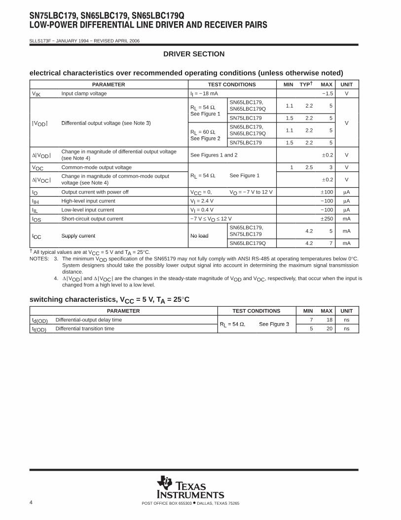
DRIVER SECTION
electrical characteristics over recommended operating conditions (unless otherwise noted)
PARAMETER TEST CONDITIONS MIN TYP† MAX UNIT
VIK Input clamp voltage II = −18 mA −1.5 V
RL = 54 Ω,See Figure 1
SN65LBC179,SN65LBC179Q
1.1 2.2 5
|VOD| Differential output voltage (see Note 3)
LSee Figure 1
SN75LBC179 1.5 2.2 5V|VOD| Differential output voltage (see Note 3)
RL = 60 Ω,See Figure 2
SN65LBC179,SN65LBC179Q
1.1 2.2 5V
LSee Figure 2
SN75LBC179 1.5 2.2 5
∆|VOD|Change in magnitude of differential output voltage(see Note 4)
See Figures 1 and 2 ±0.2 V
VOC Common-mode output voltage 1 2.5 3 V
∆|VOC|Change in magnitude of common-mode outputvoltage (see Note 4)
RL = 54 Ω, See Figure 1±0.2 V
IO Output current with power off VCC = 0, VO = −7 V to 12 V ±100 µA
IIH High-level input current VI = 2.4 V −100 µA
IIL Low-level input current VI = 0.4 V −100 µA
IOS Short-circuit output current −7 V ≤ VO ≤ 12 V ±250 mA
ICC Supply current No load
SN65LBC179,SN75LBC179
4.2 5 mAICC Supply current No load
SN65LBC179Q 4.2 7 mA† All typical values are at VCC = 5 V and TA = 25°C.NOTES: 3. The minimum VOD specification of the SN65179 may not fully comply with ANSI RS-485 at operating temperatures below 0°C.
System designers should take the possibly lower output signal into account in determining the maximum signal transmissiondistance.
4. ∆ |VOD| and ∆ |VOC| are the changes in the steady-state magnitude of VOD and VOC, respectively, that occur when the input ischanged from a high level to a low level.
switching characteristics, V CC = 5 V, TA = 25°CPARAMETER TEST CONDITIONS MIN MAX UNIT
td(OD) Differential-output delay timeRL = 54 Ω See Figure 3
7 18 ns
tt(OD) Differential transition timeRL = 54 Ω, See Figure 3
5 20 ns

SLLS173F − JANUARY 1994 − REVISED APRIL 2006
5POST OFFICE BOX 655303 • DALLAS, TEXAS 75265
RECEIVER SECTION
electrical characteristics over recommended operating conditions (unless otherwise noted)
PARAMETER TEST CONDITIONS MIN TYP MAX UNIT
VIT+ Positive-going input threshold voltage IO = −8 mA 0.2 V
VIT− Negative-going input threshold voltage IO = 8 mA −0.2 V
Vhys Hysteresis voltage (VIT+ − VIT−) 45 mV
VOH High-level output voltage VID = 200 mV, IOH = −8 mA 3.5 4.5 V
VOL Low-level output voltage VID = −200 mV, IOL = 8 mA 0.3 0.5 V
VI = 12 V,Other inputs at 0 V,
SN65LBC179,SN75LBC179
0.7 1 mAOther inputs at 0 V,VCC = 5 V SN65LBC179Q 0.7 1.2 mA
VI = 12 V,Other inputs at 0 V,
SN65LBC179,SN75LBC179
0.8 1 mA
II Bus input current
Other inputs at 0 V,VCC = 0 V SN65LBC179Q 0.8 1 .2 mA
II Bus input currentVI = −7 V,Other inputs at 0 V,
SN65LBC179,SN75LBC179
−0.5 −0.8 mAOther inputs at 0 V,VCC = 5 V SN65LBC179Q −0.5 −1.0 mA
VI = −7 V,Other inputs at 0 V,
SN65LBC179,SN75LBC179
−0.5 −0.8 mAOther inputs at 0 V,VCC = 0 V SN65LBC179Q −0.5 −1.0 mA
switching characteristics, V CC = 5 V, TA = 25°CPARAMETER TEST CONDITIONS MIN TYP MAX UNIT
tPHL Propagation delay time, high- to low-level outputVID = −1.5 V to 1.5 V, See Figure 4
15 30 ns
tPLH Propagation delay time, low- to high-level outputVID = −1.5 V to 1.5 V, See Figure 4
15 30 ns
tsk(p) Pulse skew ( tPHL − tPLH )See Figure 4
3 6 ns
tt Transition timeSee Figure 4
3 5 ns
PARAMETER MEASUREMENT INFORMATION
VOD
RL2
0 V or 3 V
Z
D
Y
RL2 VOC
Figure 1. Differential and Common-Mode Output Voltage Test Circuit

SLLS173F − JANUARY 1994 − REVISED APRIL 2006
6 POST OFFICE BOX 655303 • DALLAS, TEXAS 75265
PARAMETER MEASUREMENT INFORMATION
VOD
Vtest
R1375 Ω
0 V or 3 V
Z
D
R2375 Ω
Vtest
Y
RL = 60 Ω
−7 V < Vtest < 12 V
Figure 2. Differential Output Voltage Test Circuit
0 V
3 V
tt(OD)tt(OD)
1.5 V
td(ODH)
50%Output
Input
TEST CIRCUIT VOLTAGE WAVEFORMS
td(ODL)
RL = 54 ΩOutput
Generator(see Note A) 50 Ω
1.5 V
50%≈ 2.5 V
≈ − 2.5 V
CL = 50 pF(see Note B)
1.5 V
NOTES: A. The input pulse is supplied by a generator having the following characteristics: PRR ≤ 1 MHz, 50% duty cycle, tr ≤ 6 ns, tf ≤ 6 ns,ZO = 50 Ω.
B. CL includes probe and jig capacitance.
Figure 3. Driver Test Circuits and Differential Output Delay and Transition Time Voltage Waveforms
TEST CIRCUIT VOLTAGE WAVEFORMS
VOL
VOH
3 V
0 V
tPHLtPLH
Output
Input
1.3 V
1.5 V
1.3 V
50 Ω Output
1.5 V
Generator(see Note A)
A
B
tt
90%
10%10%
90%
tt
CL = 15 pF(see Note B)
1.5 V
NOTES: A. The input pulse is supplied by a generator having the following characteristics: PRR ≤ 1 MHz, 50% duty cycle, tr ≤ 6 ns, tf ≤ 6 ns,ZO = 50 Ω.
B. CL includes probe and jig capacitance.
Figure 4. Receiver Test Circuit and Propagation Delay and Transition Time Voltage Waveforms

SLLS173F − JANUARY 1994 − REVISED APRIL 2006
7POST OFFICE BOX 655303 • DALLAS, TEXAS 75265
TYPICAL CHARACTERISTICS
2.5
1.5
1
00 10 20 30
− H
igh-
Leve
l Out
put V
olta
ge −
V
3.5
4
DRIVERHIGH-LEVEL OUTPUT VOLTAGE
vsHIGH-LEVEL OUTPUT CURRENT
5
40 50 60
V OH
IOH − High-Level Output Current − mA
4.5
3
2
0.5
VCC = 5 VTA = 25°C
2.5
1.5
1
00 20 40 60
− Lo
w-L
evel
Out
put V
olta
ge −
V
3.5
4
DRIVERLOW-LEVEL OUTPUT VOLTAGE
vsLOW-LEVEL OUTPUT CURRENT
5
80 100 120V O
L
IOL − Low-Level Output Current − mA
4.5
3
2
0.5
VCC = 5 VTA = 25°C
70 80 90 100
Figure 5 Figure 6
2
1.5
0.5
00 10 20 30 40 50 60
− D
iffer
entia
l Out
put V
olta
ge −
V
2.5
3.5
DRIVERDIFFERENTIAL OUTPUT VOLTAGE
vsOUTPUT CURRENT
4
70 80 90 100
1
3
VCC = 5 VTA = 25°C
V OD
IO − Output Current − mA
2
1.5
0.5
0− 50 − 25 0 25
2.5
DRIVERDIFFERENTIAL OUTPUT VOLTAGE
vsFREE-AIR TEMPERATURE
50 75
1
3VCC = 5 VLoad = 54 ΩVIH = 2 V
TA − Free-Air Temperature − °C100 125
− D
iffer
entia
l Out
put V
olta
ge −
VV O
D
Figure 7 Figure 8

SLLS173F − JANUARY 1994 − REVISED APRIL 2006
8 POST OFFICE BOX 655303 • DALLAS, TEXAS 75265
TYPICAL CHARACTERISTICS
2
1
00 −10 − 20 − 30
− H
igh-
Leve
l Out
put V
olta
ge −
V
3
4
RECEIVERHIGH-LEVEL OUTPUT VOLTAGE
vsHIGH-LEVEL OUTPUT CURRENT
5
− 40 − 50IOH − High-Level Output Current − mA
V OH
20
15
5
0− 50 − 25 0 25
− D
iffer
entia
l Del
ay T
imes
− n
s
DRIVERDIFFERENTIAL DELAY TIME
vsFREE-AIR TEMPERATURE
50 75
10
VCC = 5 VLoad = 54 Ω
TA − Free-Air Temperature − °C100 125
td(ODH)
td(ODL)
6VID = 200 mV
t d(O
D)
Figure 9 Figure 10
0.3
0.2
0.1
00 5 10
− Lo
w-L
evel
Out
put V
olta
ge −
V
0.4
0.5
RECEIVERLOW-LEVEL OUTPUT VOLTAGE
vsLOW-LEVEL OUTPUT CURRENT
0.6
15 20 25 30IOL − Low-Level Output Current − mA
VO
L
VCC = 5 VTA = 25°CVID = − 200 mV
0.7
0.8
0.9
1
35 40
2
1
0
− O
utpu
t Vol
tage
− V
3
4
RECEIVEROUTPUT VOLTAGE
vsDIFFERENTIAL INPUT VOLTAGE
5
VID − Differential Input Voltage − mV
VO
− 80 − 60 − 40 − 20 0 20 40 60 80
6
VIC = 12 V
VIC = 0 V
VIC = −7 V
Figure 11 Figure 12

SLLS173F − JANUARY 1994 − REVISED APRIL 2006
9POST OFFICE BOX 655303 • DALLAS, TEXAS 75265
TYPICAL CHARACTERISTICS
40
5
25
15
0
50
30
10 K 100 K 1 M 10 M 100 M
45
10
20
AVERAGE SUPPLY CURRENTvs
FREQUENCY
35
60
55
− A
vera
ge S
uppl
y C
urre
nt −
mA
I CC
f − Frequency − Hz
ÎÎÎÎÎÎÎÎÎÎÎÎÎÎÎÎÎÎÎÎÎÎÎÎÎÎÎÎÎÎÎÎÎÎÎÎÎÎÎÎÎÎÎÎÎÎÎÎÎÎÎÎÎÎÎÎÎÎÎÎÎÎÎÎÎÎÎÎÎÎÎÎÎÎÎÎÎÎÎÎÎÎÎÎÎÎÎÎÎÎÎÎÎÎÎÎÎÎÎÎÎÎÎÎÎÎÎÎÎÎÎÎÎÎÎÎÎÎÎÎÎÎÎÎÎÎÎÎÎÎÎÎÎÎÎÎÎÎÎÎÎÎÎÎÎÎÎÎÎÎÎÎÎÎÎÎÎÎÎÎÎÎÎÎÎÎÎÎÎÎÎÎÎÎÎÎÎÎÎÎÎÎ
− 0.4
− 0.6
− 0.8
− 1− 8 − 6 − 4 − 2 0 2
− In
put C
urre
nt −
mA
− 0.2
0
RECEIVERINPUT CURRENT
vsINPUT VOLTAGE
(COMPLEMENTARY INPUT AT 0 V)
0.2
4 6 8 10 12
0.4
0.6
0.8
I I
VI − Input Voltage − V
1TA = 25°CVCC = 5 V
The shaded region of this graph representsmore than 1 unit load per RS-485.
Receiver Load = 50 pFDriver Load = Receiver Inputs
Figure 13 Figure 14
23.5
23
22.5
22− 40 − 20 0 20 40 60
− P
ropa
gatio
n D
elay
Tim
e −
ns
24
24.5
RECEIVERPROPAGATION DELAY TIME
vsFREE-AIR TEMPERATURE
80 100
TA − Free-Air Temperature − °C
tPHL
tPLH
VCC = 5 VCL = 15 pFVIO = ±1.5 V
t pd
Figure 15

SLLS173F − JANUARY 1994 − REVISED APRIL 2006
10 POST OFFICE BOX 655303 • DALLAS, TEXAS 75265
THERMAL CHARACTERISTICS − D PACKAGE
PARAMETER TEST CONDITIONS MIN TYP MAX UNIT
Junction−to−ambient thermal reisistance, θJA†Low-K board, no air flow 199.4
Junction−to−ambient thermal reisistance, θJA†High-K board, no air flow 119
°C/WJunction−to−board thermal reisistance, θJB High-K board, no air flow 67
°C/W
Junction−to−case thermal reisistance, θJC 46.6
Average power dissipation, P(AVG)
RL = 54 Ω, input to D is 10 Mbps 50% dutycycle square wave, VCC = 5.25 V, TJ = 130°C.
330 mW
Thermal shutdown junction temperature, TSD 165 °C† See TI application note literature number SZZA003, Package Thermal Characterization Methodologies, for an explanation of this parameter.

SLLS173F − JANUARY 1994 − REVISED APRIL 2006
11POST OFFICE BOX 655303 • DALLAS, TEXAS 75265
THERMAL CHARACTERISTICS OF IC PACKAGES
ΘJA (Junction-to-Ambient Thermal Resistance) is defined as the difference in junction temperature to ambient temperaturedivided by the operating power
ΘJA is NOT a constant and is a strong function of
the PCB design (50% variation)
altitude (20% variation)
device power (5% variation)
ΘJA can be used to compare the thermal performance of packages if the specific test conditions are defined and used.Standardized testing includes specification of PCB construction, test chamber volume, sensor locations, and the thermalcharacteristics of holding fixtures. ΘJA is often misused when it is used to calculate junction temperatures for otherinstallations.
TI uses two test PCBs as defined by JEDEC specifications. The low-k board gives average in-use condition thermalperformance and consists of a single trace layer 25 mm long and 2-oz thick copper. The high-k board gives best case in−usecondition and consists of two 1-oz buried power planes with a single trace layer 25 mm long with 2-oz thick copper. A 4%to 50% difference in ΘJA can be measured between these two test cards
ΘJC (Junction-to-Case Thermal Resistance) is defined as difference in junction temperature to case divided by theoperating power. It is measured by putting the mounted package up against a copper block cold plate to force heat to flowfrom die, through the mold compound into the copper block.
ΘJC is a useful thermal characteristic when a heatsink is applied to package. It is NOT a useful characteristic to predictjunction temperature as it provides pessimistic numbers if the case temperature is measured in a non-standard system andjunction temperatures are backed out. It can be used with ΘJB in 1-dimensional thermal simulation of a package system.
ΘJB (Junction-to-Board Thermal Resistance) is defined to be the difference in the junction temperature and the PCBtemperature at the center of the package (closest to the die) when the PCB is clamped in a cold−plate structure. ΘJB is onlydefined for the high-k test card.
ΘJB provides an overall thermal resistance between the die and the PCB. It includes a bit of the PCB thermal resistance(especially for BGA’s with thermal balls) and can be used for simple 1-dimensional network analysis of package system(see Figure 16).
Surface Node
JC Calculated/Measured
Junction
JB Calculated/Measured
PC Board
CA Calculated
Ambient Node
Figure 16. Thermal Resistance
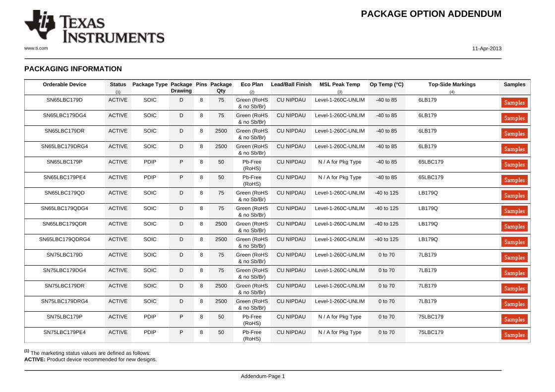
PACKAGE OPTION ADDENDUM
www.ti.com 11-Apr-2013
Addendum-Page 1
PACKAGING INFORMATION
Orderable Device Status(1)
Package Type PackageDrawing
Pins PackageQty
Eco Plan(2)
Lead/Ball Finish MSL Peak Temp(3)
Op Temp (°C) Top-Side Markings(4)
Samples
SN65LBC179D ACTIVE SOIC D 8 75 Green (RoHS& no Sb/Br)
CU NIPDAU Level-1-260C-UNLIM -40 to 85 6LB179
SN65LBC179DG4 ACTIVE SOIC D 8 75 Green (RoHS& no Sb/Br)
CU NIPDAU Level-1-260C-UNLIM -40 to 85 6LB179
SN65LBC179DR ACTIVE SOIC D 8 2500 Green (RoHS& no Sb/Br)
CU NIPDAU Level-1-260C-UNLIM -40 to 85 6LB179
SN65LBC179DRG4 ACTIVE SOIC D 8 2500 Green (RoHS& no Sb/Br)
CU NIPDAU Level-1-260C-UNLIM -40 to 85 6LB179
SN65LBC179P ACTIVE PDIP P 8 50 Pb-Free(RoHS)
CU NIPDAU N / A for Pkg Type -40 to 85 65LBC179
SN65LBC179PE4 ACTIVE PDIP P 8 50 Pb-Free(RoHS)
CU NIPDAU N / A for Pkg Type -40 to 85 65LBC179
SN65LBC179QD ACTIVE SOIC D 8 75 Green (RoHS& no Sb/Br)
CU NIPDAU Level-1-260C-UNLIM -40 to 125 LB179Q
SN65LBC179QDG4 ACTIVE SOIC D 8 75 Green (RoHS& no Sb/Br)
CU NIPDAU Level-1-260C-UNLIM -40 to 125 LB179Q
SN65LBC179QDR ACTIVE SOIC D 8 2500 Green (RoHS& no Sb/Br)
CU NIPDAU Level-1-260C-UNLIM -40 to 125 LB179Q
SN65LBC179QDRG4 ACTIVE SOIC D 8 2500 Green (RoHS& no Sb/Br)
CU NIPDAU Level-1-260C-UNLIM -40 to 125 LB179Q
SN75LBC179D ACTIVE SOIC D 8 75 Green (RoHS& no Sb/Br)
CU NIPDAU Level-1-260C-UNLIM 0 to 70 7LB179
SN75LBC179DG4 ACTIVE SOIC D 8 75 Green (RoHS& no Sb/Br)
CU NIPDAU Level-1-260C-UNLIM 0 to 70 7LB179
SN75LBC179DR ACTIVE SOIC D 8 2500 Green (RoHS& no Sb/Br)
CU NIPDAU Level-1-260C-UNLIM 0 to 70 7LB179
SN75LBC179DRG4 ACTIVE SOIC D 8 2500 Green (RoHS& no Sb/Br)
CU NIPDAU Level-1-260C-UNLIM 0 to 70 7LB179
SN75LBC179P ACTIVE PDIP P 8 50 Pb-Free(RoHS)
CU NIPDAU N / A for Pkg Type 0 to 70 75LBC179
SN75LBC179PE4 ACTIVE PDIP P 8 50 Pb-Free(RoHS)
CU NIPDAU N / A for Pkg Type 0 to 70 75LBC179
(1) The marketing status values are defined as follows:ACTIVE: Product device recommended for new designs.

PACKAGE OPTION ADDENDUM
www.ti.com 11-Apr-2013
Addendum-Page 2
LIFEBUY: TI has announced that the device will be discontinued, and a lifetime-buy period is in effect.NRND: Not recommended for new designs. Device is in production to support existing customers, but TI does not recommend using this part in a new design.PREVIEW: Device has been announced but is not in production. Samples may or may not be available.OBSOLETE: TI has discontinued the production of the device.
(2) Eco Plan - The planned eco-friendly classification: Pb-Free (RoHS), Pb-Free (RoHS Exempt), or Green (RoHS & no Sb/Br) - please check http://www.ti.com/productcontent for the latest availabilityinformation and additional product content details.TBD: The Pb-Free/Green conversion plan has not been defined.Pb-Free (RoHS): TI's terms "Lead-Free" or "Pb-Free" mean semiconductor products that are compatible with the current RoHS requirements for all 6 substances, including the requirement thatlead not exceed 0.1% by weight in homogeneous materials. Where designed to be soldered at high temperatures, TI Pb-Free products are suitable for use in specified lead-free processes.Pb-Free (RoHS Exempt): This component has a RoHS exemption for either 1) lead-based flip-chip solder bumps used between the die and package, or 2) lead-based die adhesive used betweenthe die and leadframe. The component is otherwise considered Pb-Free (RoHS compatible) as defined above.Green (RoHS & no Sb/Br): TI defines "Green" to mean Pb-Free (RoHS compatible), and free of Bromine (Br) and Antimony (Sb) based flame retardants (Br or Sb do not exceed 0.1% by weightin homogeneous material)
(3) MSL, Peak Temp. -- The Moisture Sensitivity Level rating according to the JEDEC industry standard classifications, and peak solder temperature.
(4) Multiple Top-Side Markings will be inside parentheses. Only one Top-Side Marking contained in parentheses and separated by a "~" will appear on a device. If a line is indented then it is acontinuation of the previous line and the two combined represent the entire Top-Side Marking for that device.
Important Information and Disclaimer:The information provided on this page represents TI's knowledge and belief as of the date that it is provided. TI bases its knowledge and belief on informationprovided by third parties, and makes no representation or warranty as to the accuracy of such information. Efforts are underway to better integrate information from third parties. TI has taken andcontinues to take reasonable steps to provide representative and accurate information but may not have conducted destructive testing or chemical analysis on incoming materials and chemicals.TI and TI suppliers consider certain information to be proprietary, and thus CAS numbers and other limited information may not be available for release.
In no event shall TI's liability arising out of such information exceed the total purchase price of the TI part(s) at issue in this document sold by TI to Customer on an annual basis.
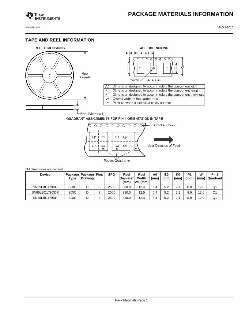
TAPE AND REEL INFORMATION
*All dimensions are nominal
Device PackageType
PackageDrawing
Pins SPQ ReelDiameter
(mm)
ReelWidth
W1 (mm)
A0(mm)
B0(mm)
K0(mm)
P1(mm)
W(mm)
Pin1Quadrant
SN65LBC179DR SOIC D 8 2500 330.0 12.4 6.4 5.2 2.1 8.0 12.0 Q1
SN65LBC179QDR SOIC D 8 2500 330.0 12.5 6.4 5.2 2.1 8.0 12.0 Q1
SN75LBC179DR SOIC D 8 2500 330.0 12.4 6.4 5.2 2.1 8.0 12.0 Q1
PACKAGE MATERIALS INFORMATION
www.ti.com 18-Oct-2016
Pack Materials-Page 1

*All dimensions are nominal
Device Package Type Package Drawing Pins SPQ Length (mm) Width (mm) Height (mm)
SN65LBC179DR SOIC D 8 2500 340.5 338.1 20.6
SN65LBC179QDR SOIC D 8 2500 340.5 338.1 20.6
SN75LBC179DR SOIC D 8 2500 340.5 338.1 20.6
PACKAGE MATERIALS INFORMATION
www.ti.com 18-Oct-2016
Pack Materials-Page 2


IMPORTANT NOTICE
Texas Instruments Incorporated and its subsidiaries (TI) reserve the right to make corrections, enhancements, improvements and otherchanges to its semiconductor products and services per JESD46, latest issue, and to discontinue any product or service per JESD48, latestissue. Buyers should obtain the latest relevant information before placing orders and should verify that such information is current andcomplete. All semiconductor products (also referred to herein as “components”) are sold subject to TI’s terms and conditions of salesupplied at the time of order acknowledgment.TI warrants performance of its components to the specifications applicable at the time of sale, in accordance with the warranty in TI’s termsand conditions of sale of semiconductor products. Testing and other quality control techniques are used to the extent TI deems necessaryto support this warranty. Except where mandated by applicable law, testing of all parameters of each component is not necessarilyperformed.TI assumes no liability for applications assistance or the design of Buyers’ products. Buyers are responsible for their products andapplications using TI components. To minimize the risks associated with Buyers’ products and applications, Buyers should provideadequate design and operating safeguards.TI does not warrant or represent that any license, either express or implied, is granted under any patent right, copyright, mask work right, orother intellectual property right relating to any combination, machine, or process in which TI components or services are used. Informationpublished by TI regarding third-party products or services does not constitute a license to use such products or services or a warranty orendorsement thereof. Use of such information may require a license from a third party under the patents or other intellectual property of thethird party, or a license from TI under the patents or other intellectual property of TI.Reproduction of significant portions of TI information in TI data books or data sheets is permissible only if reproduction is without alterationand is accompanied by all associated warranties, conditions, limitations, and notices. TI is not responsible or liable for such altereddocumentation. Information of third parties may be subject to additional restrictions.Resale of TI components or services with statements different from or beyond the parameters stated by TI for that component or servicevoids all express and any implied warranties for the associated TI component or service and is an unfair and deceptive business practice.TI is not responsible or liable for any such statements.Buyer acknowledges and agrees that it is solely responsible for compliance with all legal, regulatory and safety-related requirementsconcerning its products, and any use of TI components in its applications, notwithstanding any applications-related information or supportthat may be provided by TI. Buyer represents and agrees that it has all the necessary expertise to create and implement safeguards whichanticipate dangerous consequences of failures, monitor failures and their consequences, lessen the likelihood of failures that might causeharm and take appropriate remedial actions. Buyer will fully indemnify TI and its representatives against any damages arising out of the useof any TI components in safety-critical applications.In some cases, TI components may be promoted specifically to facilitate safety-related applications. With such components, TI’s goal is tohelp enable customers to design and create their own end-product solutions that meet applicable functional safety standards andrequirements. Nonetheless, such components are subject to these terms.No TI components are authorized for use in FDA Class III (or similar life-critical medical equipment) unless authorized officers of the partieshave executed a special agreement specifically governing such use.Only those TI components which TI has specifically designated as military grade or “enhanced plastic” are designed and intended for use inmilitary/aerospace applications or environments. Buyer acknowledges and agrees that any military or aerospace use of TI componentswhich have not been so designated is solely at the Buyer's risk, and that Buyer is solely responsible for compliance with all legal andregulatory requirements in connection with such use.TI has specifically designated certain components as meeting ISO/TS16949 requirements, mainly for automotive use. In any case of use ofnon-designated products, TI will not be responsible for any failure to meet ISO/TS16949.
Products ApplicationsAudio www.ti.com/audio Automotive and Transportation www.ti.com/automotiveAmplifiers amplifier.ti.com Communications and Telecom www.ti.com/communicationsData Converters dataconverter.ti.com Computers and Peripherals www.ti.com/computersDLP® Products www.dlp.com Consumer Electronics www.ti.com/consumer-appsDSP dsp.ti.com Energy and Lighting www.ti.com/energyClocks and Timers www.ti.com/clocks Industrial www.ti.com/industrialInterface interface.ti.com Medical www.ti.com/medicalLogic logic.ti.com Security www.ti.com/securityPower Mgmt power.ti.com Space, Avionics and Defense www.ti.com/space-avionics-defenseMicrocontrollers microcontroller.ti.com Video and Imaging www.ti.com/videoRFID www.ti-rfid.comOMAP Applications Processors www.ti.com/omap TI E2E Community e2e.ti.comWireless Connectivity www.ti.com/wirelessconnectivity
Mailing Address: Texas Instruments, Post Office Box 655303, Dallas, Texas 75265Copyright © 2016, Texas Instruments Incorporated