Embed Size (px)
Citation preview

Japan Advanced Institute of Science and Technology
JAIST Repositoryhttps://dspace.jaist.ac.jp/
Title
Low Temperature Heteroepitaxial Growth of a New
Phase Lead Zirconate Titanate Film on Si
Substrate with an Epitaxial (ZrO_2)_<1-
x>(Y_2O_3)_x Buffer Layer
Author(s) Horita, Susumu; Aikawa, Mami; Naruse, Tetsuya
CitationJapanese Journal of Applied Physics, 39: 4860-
4868
Issue Date 2000
Type Journal Article
Text version author
URL http://hdl.handle.net/10119/9600
Rights
This is the author's version of the work. It is
posted here by permission of The Japan Society of
Applied Physics. Copyright (C) 2000 The Japan
Society of Applied Physics.
Description

Low Temperature Heteroepitaxial Growth of a New Phase Lead Zirconate
Titanate Film on Si Substrate with an Epitaxial (Zr02hサ (Y203)x Buffer Layer
Susumu HORIτ吋MamiAIKAWA and Tetsuya NARUSE
School of Mater・ialsScieηce, Japαn Advαnced Institute of Sc白nceαndTechnology, Hokurik叫 Tatsunokuchi,Ishikαωα923世
1292, Japαn
(Received date; revised manuscript received date; accepted for publication date These dates will be written in by the editor, hence please let these lines remain unchanged even though your preprint looks a bit ugly.)
We investigated the crystalline and eledrica1 properties of heteroepitaxia1 1ead zirconate titanate (PZT)五1ms
grown on Si covered with epitaxia1 (100) (Zr02hーバY203)x(YSZ)buffer 1ayers. The PZT fi1ms were prepared by
reactive sputtering. When the substrate temperature was between 400 and 4850C, we obtained a heteroepitaxia1
(110) oriented monocli山 PZT(m“PZT)五1mwhich was metastab1e. The 1attice parameters were as follows:
α b 0.379 nm, c 0.521 nm and γ= 81.30• The m-PZT五1mhad a 1arger oxygen composition ratio
0/ (Zr+ Ti) of 3.2 to 3.8 than the perovskite phase. Although the resistivity of the 邸側grownm田 PZT五1mw部
much 10wer than that of the norma1 perovskite phase, it was increased by two to五veorders of magnitude by a
step-annealing process of 3000C for 120 min, 3250C for 120 min and 3500C for 180 min in sequence. From the c -V characteristics of the step.噸輔叫耐剛向
to be about 45.
KEYWORDS: PZT, YSZ, Si, heteroepitaxy, sputtering, monoclinic
l
Low Temperature Heteroepitaxial Growth of a New Phase Lead Zirconate Titanate Film on Si Substrate with an Epitaxial (Zr02h-x(Y203)x Buffer Layer
Susumu HORITA,* Mami AIKAWA and Tetsuya NARUSE
School of Materials Science, Japan Advanced Institute of Science and Technology, Hokuriku, Tatsunokuchi, Ishikawa 923-1292, Japan
(Received date; revised manuscript received date; accepted for publication date These dates will be written in by the editor, hence please let these lines remain unchanged even though your preprint looks a bit ugly.)
We investigated the crystalline and electrical properties of heteroepitaxial lead zirconate titanate (PZT) films grown on Si covered with epitaxial (100) (Zr02h-x(Y2 03)x(YSZ) buffer layers. The PZT films were prepared by reactive sputtering. When the substrate temperature was between 400 and 485°C, we obtained a heteroepitaxial (110) oriented monoclinic PZT (m-PZT) film which was metastable. The lattice parameters were as follows: a = b = 0.379 nm, C = 0.521 nm and ,. = 81.3°. The m-PZT film had a larger oxygen composition ratio O/(Zr+Ti) of 3.2 to 3.8 than the perovskite phase. Although the resistivity of the as-grown m-PZT film was much lower than that of the normal perovskite phase, it was increased by two to five orders of magnitude by a step-annealing process of 300°C for 120 min, 325°C for 120 min and 350°C for 180 min in sequence. From the C- V characteristics ofthe step-annealed m-PZT/YSZ/Si structure, the relative dielectric constant was estimated to be about 45.
KEYWORDS: PZT, YSZ, Si, heteroepitaxy, sputtering, monoclinic
1

1. In土roduction
Lead zirconate titanate Pb(Zra Th-a)03(PZT) has re-cently been studied as a promising material for capaci-tors in ferroelectric rando世 accessmemories (F武A地)and for gate dielectric i叩 llatorsin metal/ferroelectric/ semiconductor field四 effecttransistors (MFS-FETs ).1,2)
MFS-FETs, in which the gate is controlled by sponta-neous polarization of ferroelectric materials, have the features of high switching speed, nonvolatility, radiation tolerance and high density. To realize MFS-FETs, it is necessary to fabricate PZT films directly on semicon-ductor substrates, in particular, on Si. However, this is very di由cu1tbecause Pb reacts with Si and eωily dif-fuses into the Si substrate.3) 1n order to overcome this di缶culty,several researchers attempted to use several dielectric materials, e. 9・, Ce02,2) MgO,4, 5) SrTi03,6) CeaZr1-a02,7)Y2038) and Zr029) as a buffer layer in-serted between the PZT film and the Si substrate. On the other hand, a single crystal film is expected to ex-hibit high stability, uniformity of material properties and high performance of electron device.10,11) 1n order to obtain an epitaxial single crystal PZT film, the buffer layer should be a single crystal film. Thus, we have pro-posed the use of a heteroepitaxial yttriaωstabilized zirco-nia [YSZ;(Zr02h-a(Y203)a] film as a buffer layer.叫 同
YSZ is a very attractive electrical insulator because it has high chemical stability, high resistivity and a large relative dielectric constant of about 30, and can be het-eroepit砿 iallygrown on Si.14)宜iraiet al. used a YSZ layer as a buffer layer for PbTi03 on Si.
15) Also, we have reported that an epitaxial PZT film on Si can be obtained with a 10-nm-thick epitaxial YSZ layer.12) 1n order to op-erate MF1S-FET at a lower voltage in future 1Cs, it is necessary to make the YSZ buffer layer as thin as pos-sible. However, because decre邸 ingthe thickness of the YSZ buffer layer leads to a reduction in its ability to pre“
vent the diffusion of Pb into the Si substrate, the growth temperature of the PZT film has to be lowered. Also, the low temperature growth technique has the advan-tage of controlling the Pb content of the film more .easily than the high temperature growth because it suppresses the re但 evaporationof Pb and Pb oxides from the deposi“
tion surface.16,17) Thus, we attempted the low tempera-ture deposition of PZT film on an epitaxial YSZ layer by rf magnetron sputtering and obtained an epitaxial PZT
2. Experimental
YSZ buffer layers were deposited on n-type (100) Si substrates by dc magnetron reactive sputtering with Ar十O2gas and a metallic target. The resistivity of the substrate was 0.005-0.01 Qcm. Generally, the heteroepi句
*E-mail address: horita@jaist・すjp
1. Introduction
Lead zirconate titanate Pb(Zra: Th-a:)03(PZT) has recently been studied as a promising material for capacitors in ferroelectric random-access memories (FRAMs) and for gate dielectric insulators in metal/ferroelectric/ semiconductor field-effect transistors (MFS- FETs ).1,2) MFS-FETs, in which the gate is controlled by spontaneous polarization of ferroelectric materials, have the features of high switching speed, nonvolatility, radiation tolerance and high density. To realize MFS-FETs, it is necessary to fabricate PZT films directly on semiconductor substrates, in particular, on Si. However, this is very difficult because Pb reacts with Si and easily diffuses into the Si substrate.3) In order to overcome this difficulty, several researchers attempted to use several dielectric materials, e.g., Ce02,2) MgO,4,5) SrTi03,6) Cea:Zr1-a:02,7)Y2038) and Zr029) as a buffer layer inserted between the PZT film and the Si substrate. On the other hand, a single crystal film is expected to exhibit high stability, uniformity of material properties and high performance of electron device. 10, 11) In order to obtain an epitaxial single crystal PZT film, the buffer layer should be a single crystal film. Thus, we have proposed the use of a heteroepitaxial yttria- stabilized zirconia [YSZ;(Zr02h-a:(Y203)a:] film as a buffer layer.12, 13) YSZ is a very attractive electrical insulator because it has high chemical stability, high resistivity and a large relative dielectric constant of about 30, and can be heteroepitaxially grown on Si.14) Hirai et al. used a YSZ layer as a buffer layer for PbTi03 on Si.15) Also, we have reported that an epitaxial PZT film on Si can be obtained with a 10-nm-thick epitaxial YSZ layer.12) In order to operate MFIS-FET at a lower voltage in future ICs, it is necessary to make the YSZ buffer layer as thin as possible. However, because decreasing the thickness of the YSZ buffer layer leads to a reduction in its ability to prevent the diffusion of Pb into the Si substrate, the growth temperature of the PZT film has to be lowered. Also, the low temperature growth technique has the advantage of controlling the Pb content of the film more .easily than the high temperature growth because it suppresses the re-evaporation of Pb and Pb oxides from the deposition surface. 16, 17) Thus, we attempted the low temperature deposition of PZT film on an epitaxial YSZ layer by rf magnetron sputtering and obtained an epitaxial PZT film at substrate temperatures as low as 435°C. However, this epitaxial PZT film showed material properties different from those of a perovskite PZT film. In order to improve electrical insulation, we annealed the deposited PZT films. In this paper, we report the crystalline properties, electrical properties and chemical composition of as-grown and annealed PZT films, and discuss the experimental results.
2. Experimental
YSZ buffer layers were deposited on n-type (100) Si substrates by dc magnetron reactive sputtering with Ar+02 gas and a metallic target. The resistivity of the substrate was 0.005-0.01 ncm. Generally, the heteroepi-
*E-mail address:[email protected] 2

taxial growth of a YSZ layer on Si by reactive sput-tering is difficult because the bare Si surface is easily oxidized by plωma radiation or excited oxygen atoms prior to the deposition of the YSZ layer. As a solution
to this problem, we used the following process: the Si surface is weakly oxidized, followed by deposition of a
very thin metallic Zrl-m Y m film prior to the deposition of a YSZ layer. The details of this process are shown elsewhere.18) The thickness of the YSZ layer was about
10 or 100 nm and the yttria content wωestimated to be about 14 mol% by X-ray photoelectron spectroscopy (XPS) measurement with a山 ndardsample. The PZT film was deposited on the YSZ/Si structure by rf mag-netron reactive sputtering. We used aιinch-diameter
stoichiometric Pb(ZrO.52Tio.48)03 disc as a sputtering target. Since the substrate temperature was relatively low, 435同 5200C,it was expected that the re-evaporation of Pb and PbO from the deposition surface was sup-pressed so that the composition of the deposited film became nearly equal to that of the target.19) The sub-strate was heated by fl.owing electric curren t through the tantalum electrodes attached to the substrate. The typ-ical sputtering conditions were as follows: the discharge
pressure of Ar+02 gas was 2 Pa, the O2/ Ar fl.ow rate r仕tio was 1/10 and the rf power was 100 W. The thickness of the PZT film was 100 or 200 nm. In order to improve the electrical properties of the as-grown PZT films, some ofthem were 出 mealedat a temperature of 300 to 4000C in O2 atmosphere.
The crystallographic properties of the PZT films were investigated by X司 raydiffraction (XRD) analysis and Ruthe巾 rdbackscatteri時 (RBS)spectrometry with 1.6 MeV 4He+ ions. The chemical composition of the sample was also obtained by RBS measurement. Mi-cros坑tructl山1汀ralcharacterization of the samples was carried out using a tr玲&釘叩nsrLeakage current density-voltage (J -V) characteristics were measured with step voltages and the time interval of each step was 2 s. Top and bottom electrodes were formed by depositing 0.2-mm-diameter Au and Al films on the PZT film and on the back of the substrate, re-spectively.
3. Experimental Results
Figure 1 shows the substrate temperature九 deperトdence of XRD patterns of 100-or 200-nm-thick PZT films on Si with YSZ buffer layers. The thicknesses of the YSZ layers are 10 nm at Ts = 460 and 4700C, and 100 nm at Ts口 435and 4950C. The peaks due to YSZ (200) are hardly
trucial growth of a YSZ layer on Si by reactive sputtering is difficult because the bare Si surface is easily oxidized by plasma radiation or excited oxygen atoms prior to the deposition of the YSZ layer. As a solution to this problem, we used the following process: the Si surface is weakly oxidized, followed by deposition of a very thin metallic ZrI-m Y m film prior to the deposition of a YSZ layer. The details of this process are shown elsewhere. I8) The thickness of the YSZ layer was about 10 or 100 nm and the yttria content was estimated to be about 14 mol% by X-ray photoelectron spectroscopy (XPS) measurement with a standard sample. The PZT film was deposited on the YSZ/Si structure by rf magnetron reactive sputtering. We used a 4-inch-diameter stoichiometric Pb(Zro.52Tio.48)03 disc as a sputtering target. Since the substrate temperature was relatively low, 435-520°C, it was expected that the re-evaporation of Pb and PbO from the deposition surface was suppressed so that the composition of the deposited film became nearly equal to that of the target. I9) The substrate was heated by flowing electric current through the tantalum electrodes attached to the substrate. The typical sputtering conditions were as follows: the discharge pressure of Ar+02 gas was 2 Pa, the O2/ Ar flow rate ratio was 1/10 and the rf power was 100 W. The thickness of the PZT film was 100 or 200 nm. In order to improve the electrical properties of the as-grown PZT films, some of them were annealed at a temperature of 300 to 400°C in O2 atmosphere.
The crystallographic properties of the PZT films were investigated by X-ray diffraction (XRD) analysis and Rutherford backscattering (RBS) spectrometry with 1.6 MeV 4He+ ions. The chemical composition of the sample was also obtained by RBS measurement. Microstructural characterization of the samples was carried out using a transmission electron microscope (TEM). Leakage current density-voltage (J - V) characteristics were measured with step voltages and the time interval of each step was 2 s. Top and bottom electrodes were formed by depositing 0.2-mm-diameter Au and Al films on the PZT film and on the back of the substrate, respectively.
3. Experimental Results
Figure 1 shows the substrate temperature Ts dependence of XRD patterns of 100- or 200-nm-thick PZT films on Si with YSZ buffer layers. The thicknesses of the YSZ layers are 10 nm at Ts = 460 and 470°C, and 100 nm at Ts = 435 and 495°C. The peaks due to YSZ (200) are hardly observed at Ts = 460 and 470°C because they overlap with the large pyrochlore (400) peaks. We can see from this figure that strong peaks near the diffraction angle of the perovskite PZT (110) around 31 ° appear with small peaks around 34.3° due to pyrochlore (400) and 36.2°, when Ts is equal or less than 470°C. The peaks around 36.2° are not due to YSZ, PZT and PbO. On the other hand, at the higher substrate temperature Ts ;::: 495°C, the diffraction peak due to the pyrochlore (400) phase becomes strong and the peak around 31° disappears. The peak angle of this pyrochlore phase is slightly smaller than those at Ts = 460 and 470°C. This
3

phenomenon probably results from the influence of the
underlying YSZ layer and is discussed further based on the results in Fig.6. Figure 2 shows theゆsc出 1patterns
of the PZT film grown at Ts = 4350C in Fig.l. From
each pattern, we can observe peaks of four fold symmetry clearly. These patterns are very similar to those of the
perovskite (110) PZT film with a heteroepitaxial double domain structure. A similar crystallographic orientation
relation on heteroepitaxial growth has been reported for (110)Y203j(100)Si20) and (110)Ce02j(100)Si.21) How-
ever, it was found that the values of () for the measured
lattice planes were different from those of the perovskite PZT. This difference can not be explained by measure-
ment error and simple lattice deformation due to hetω eroepitaxial growth. This essentially results from the formation of an unknown PZT phase, which is explained
more clearly by means of cross-sectional TEM observa-tion as shown in Fig.6. Hereafter, this unknown PZT
phase is abbreviated to m-PZT and its structure will be discussed in greater detaillater.
Next, we estimated the chemical composition of the deposited PZT film by RBS measurement. Figure 3 shows the dependence of the composition ratio of the
deposited PZT film on the substrate temperature. The measurement error is about土5%. The substrate tem-peratures are divided into the three regions with respect to the crystallinity of the deposited PZT film. The tem-perature of the first (1) region is between room temper-ature and 4000C, where the film is almost amorphous because of the absence of XRD peaks except those of Si
and YSZ. The temperatures of the second (II) and third (II1) regions are between 400 and 4800C, and higher than 4800C, respectively. 1n the II and II1 regions, the PZT films consist of mainly unknown and pyrochlore phases, respecti vely. From this figureぅitcan be seen that the Pb ratios range from 0.9 to 1.0 and are almost stoichiometric for all three temperature regions. Also, the Ti and Zr ra-tios are roughly constant over the substrate temperature range investigated, although they approach target values with a gradual increase in substrate temperature. Some researchers have reported the same results regarding the Ti and Zr composition ratios of PZT films prepared by sputtering. 22,23) 1n contrast, the oxygen composition ra-
tio shows marked variation with substrate temperature: It is much higher in the II region than in the othe
4
巨司
Eヨ
phenomenon probably results from the influence of the underlying YSZ layer and is discussed further based on the results in Fig.5. Figure 2 shows the ¢ scan patterns of the PZT film grown at Ts = 435°C in Fig.I. From each pattern, we can observe peaks of four fold symmetry clearly. These patterns are very similar to those of the perovskite (110) PZT film with a heteroepitaxial double domain structure. A similar crystallographic orientation relation on heteroepitaxial growth has been reported for (110)Y203/(100)Si20) and (110)Ce02/(100)Si.21) However, it was found that the values of () for the measured lattice planes were different from those of the perovskite PZT. This difference can not be explained by measurement error and simple lattice deformation due to heteroepitaxial growth. This essentially results from the formation of an unknown PZT phase, which is explained more clearly by means of cross-sectional TEM observation as shown in Fig.5. Hereafter, this unknown PZT phase is abbreviated to m-PZT and its structure will be discussed in greater detail later.
Next, we estimated the chemical composition of the deposited PZT film by RBS measurement. Figure 3 shows the dependence of the composition ratio of the deposited PZT film on the substrate temperature. The measurement error is about ±5%. The substrate temperatures are divided into the three regions with respect to the crystallinity of the deposited PZT film. The temperature of the first (I) region is between room temperature and 400°C, where the film is almost amorphous because of the absence of XRD peaks except those of Si and YSZ. The temperatures of the second (II) and third (III) regions are between 400 and 480°C, and higher than 480°C, respectively. In the II and III regions, the PZT films consist of mainly unknown and pyrochlore phases, respectively. From this figure, it can be seen that the Pb ratios range from 0.9 to 1.0 and are almost stoichiometric for all three temperature regions. Also, the Ti and Zr ratios are roughly constant over the substrate temperature range investigated, although they approach target values with a gradual increase in substrate temperature. Some researchers have reported the same results regarding the Ti and Zr composition ratios of PZT films prepared by sputtering. 22,23) In contrast, the oxygen composition ratio shows marked variation with substrate temperature: It is much higher in the II region than in the other temperature regions. Also, in the III region, it is smaller than the stoichiometric ratio of the perovskite phase, which means that the deposited film contains oxygen-deficient pyrochlore phase.
In order to improve the electrical insulation of the mPZT film, we annealed the as-grown samples. When the annealing temperature and time were set at 350°C and 90 min, respectively, the (110) m-PZT peak in the XRD pattern decreased in intensity and the crystalline quality of the m-PZT film deteriorated. Although the sample annealed at 300°C for 30 min retained the m-PZT phase, electrical insulation was not sufficiently improved. Then, the sample annealed at 300°C for 30 min was annealed again at 400°C for 30 min. However, the crystalline quality of the m-PZT film degraded, accompanied by the formation of a small amount of pyrochlore phase, as
4
shown in Fig.4(a), where the 貯 PZTfilm was grown at Ts =コ 43500.From these results, we consider that the m-PZT phase is metastable叩 dmore unstable than the pyrochlore phase. In order to avoid the phase change of the m凶 PZT五1mdue to high temperature annealing, we attempted to use a step-annealing process which involves the three annealing conditions of 30000 for 120 min, 32500 for 120 min and 35000 for 180 min in sequence. Figure 4(b) shows the XRD pattern of the step-annealed sample with the PZT film grown at Ts = 46000. From this figure, it can be seen that the XRD pattern of the step明 annealedsample did not vary markedly from that of the as-grown one except for the small increase in inten-
sity of the pyrochlore (400) peak. Figures 5( a) and 5(b) show the RBS spectra of the as-grown sample (Fig.1, 九 =46000) and the step-annealed sample (Fig.4 (b)), respectively. From these figures, it can be seen that the channeling minimum yields,χmin, in the Pb band near the surface are about 60 and 90% for the as-grown and the step-annealed samples, respectively. The increase in χmin due to the step-annealing process is likewise ob“
served in the Ti and Zr bands of the PZT film. This means that the crystalline quality of the PZT五1mwas deteriorated slightly by the step-annealing process, in agreement with the XRD measurement resu1t of Fig.4. However, the inter-diffusion between the PZT film and the YSZ layer and the composition change due to the stepωannealing process are hardly observed in the r出ト
dom RBS spectra. Since the step-annealing process with the temperature higher than 35000 might induce phase change, it was not performed.
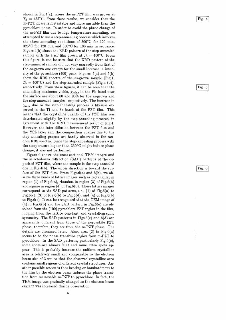
Figure 6 shows the cross世 sectionalTEM images and the selected-area diffraction (SAD) patterns of the de-posited PZT film, where the sample is the step-annealed one in Fig.4(b). The upper direction is toward the sur-face of the PZT film. From Figs.6(a) and 6(b), we ob-serve three kinds of lattice images such as rectangular in region (1) of Fig.6( a), rhombus in region (3) of Fig.6(b) and square in region (4) ofFig.6(b). These lattice images correspo註dto the SAD patterns, i. e・, (1) of Fig.6( a) to Fig.6( c), (3) of Fig.6(b) to Fig.6( d), and (4) of Fig.6(b) to Fig.6( e). It can be recognized that the TEM image of (4) in Fig.6(b) and the SAD pattern in Fig.6(e) are ob-tained from the (100) pyrochlore PZT region in the film, judging from the lattice constant and crystallographic symmetry. The SAD patterns in Figs.6(
5
巨司
I Fig. 51
医三百
shown in FigA(a), where the m-PZT film was grown at Ts = 435°0. From these results, we consider that the m-PZT phase is metastable and more unstable than the pyrochlore phase. In order to avoid the phase change of the m-PZT film due to high temperature annealing, we attempted to use a step-annealing process which involves the three annealing conditions of 300°0 for 120 min, 325°0 for 120 min and 350°0 for 180 min in sequence. Figure 4(b) shows the XRD pattern of the step-annealed sample with the PZT film grown at Ts = 460°0. From this figure, it can be seen that the XRD pattern of the step-annealed sample did not vary markedly from that of the as-grown one except for the small increase in intensity of the pyrochlore (400) peak. Figures 5( a) and 5(b) show the RBS spectra of the as-grown sample (Fig.1, Ts = 460°0) and the step-annealed sample (FigA (b)), respectively. From these figures, it can be seen that the channeling minimum yields, Xmin' in the Pb band near the surface are about 60 and 90% for the as-grown and the step-annealed samples, respectively. The increase in Xmin due to the step-annealing process is likewise observed in the Ti and Zr bands of the PZT film. This means that the crystalline quality of the PZT film was deteriorated slightly by the step-annealing process, in agreement with the XRD measurement result of FigA. However, the inter-diffusion between the PZT film and the YSZ layer and the composition change due to the step-annealing process are hardly observed in the random RBS spectra. Since the step-annealing process with the temperature higher than 350°0 might induce phase change, it was not performed.
Figure 6 shows the cross-sectional TEM images and the selected-area diffraction (SAD) patterns of the deposited PZT film, where the sample is the step-annealed one in FigA(b). The upper direction is toward the surface of the PZT film. From Figs.6(a) and 6(b), we observe three kinds of lattice images such as rectangular in region (1) of Fig.6( a), rhombus in region (3) of Fig.6(b) and square in region (4) ofFig.6(b). These lattice images correspond to the SAD patterns, i.e., (1) of Fig.6(a) to Fig.6( c), (3) of Fig.6(b) to Fig.6( d), and (4) of Fig.6(b) to Fig.6( e). It can be recognized that the TEM image of (4) in Fig.6(b) and the SAD pattern in Fig.6(e) are obtained from the (100) pyrochlore PZT region in the film, judging from the lattice constant and crystallographic symmetry. The SAD patterns in Figs.6( c) and 6( d) are apparently different from those of the perovskite PZT phase; therefore, they are from the m-PZT phase. The details are discussed later. Also, area (2) in Fig.6(a) seems to be the phase transition region from m-PZT to pyrochlore. In the SAD patterns, particularly Fig.6( c), some spots are almost faint and some extra spots appear. This is probably because the uniform crystalline area is relatively small and comparable to the electron beam size of 3 nm so that the observed crystalline area contains small regions of differ.ent crystal structures. Another possible reason is that heating or bombardment to the film by the electron beam induces the phase transition from metastable m-PZT to pyrochlore. In fact, the TEM image was gradually changed as the electron beam current was increased during observation.
5
I Fig. 51
On the other hand, the cross-sectional TEM image also shows that most of an about 20-nm-thick interfa-ciallayer from the YSZ layer is pyrochlore phase. If this pyrochlore layer grew from the YSZ film, the phase of the growing film would not change from pyrochlore to m-PZT and all of the film would have the pyrochlore phase. This is because the pyrochlore phase is stabler than the m-PZT phase as mentioned above. Thus, it can be con-sidered that this pyrochlore interfaciallayer was formed due to the phase transition of the rrトPZTphase film. It is also supposed that this transition occurred not during the step司 annealingprocess but during the deposition or the cooling process after the deposition since the region
comprisi時 thislayer is as large as about 1/5 of the en-tire PZT film and the pyrochlore peak intensity in the XRD pattern was not so increased by the step司 annealingprocess as shown in Fig.4(b). As a candidate force that induces the phase transition, we have film stress due to the differences in the lattice constant and the thermal expansion coe龍cientbetween YSZ and PZT. ]ヨasedon this consideration, we can explain the small difference in pyrochlore peak angle between the XRD patterns ob-tained at 4950C and 460 or 4700C, as shown in Fig.1, as follows: It can be deduced from the above discussion that the pyrochlore peaks at 460 and 4700C are mainly due to the pyrochlore interfacial layer. This thin interfacial layer is so strongly influenced by the YSZ layer that it may be slightly deformed. However, since the PZT film grown at 4950C is entirely pyrochlore with a thickness of 200 nm, the deformed structure in the interface is negli-gible compared with the entire average crystal structure. Therefore, the XRD peak angle due to the pyrochlore phase at 4950C is slightly di官'erentfrom those at 460 and 4700C.
Figure 7 shows the leakage current characteristics of the as-grown sample with a 10悶 nm-thickYSZ buffer layer at Ts口 4600Cand the step-annealed sample shown in Fig.4(b). We can see that the leakage current of the as-grown sample is much higher than that of a normal per向
。vskite五1m.This leakage current was as high as that of the as-grown m-PZT五1meven with a 100-nm-thick YSZ buffer layer. Also, the leakage current of a 10-nm-thick YSZ/Si structure was lower than 10-7 A/cm2 at 0.5 V. These results suggest that the resistivity of the as-grown m-PZT film should be sufficiently low that the leakage current of the
巨司
On the other hand, the cross-sectional TEM image also shows that most of an about 20-nm-thick interfaciallayer from the YSZ layer is pyrochlore phase. If this pyrochlore layer grew from the YSZ film, the phase of the growing film would not change from pyrochlore to mPZT and all of the film would have the pyrochlore phase. This is because the pyrochlore phase is stabler than the m-PZT phase as mentioned above. Thus, it can be considered that this pyrochlore interfacial layer was formed due to the phase transition of the m-PZT phase film. It is also supposed that this transition occurred not during the step-annealing process but during the deposition or the cooling process after the deposition since the region comprising this layer is as large as about 1/5 of the entire PZT film and the pyrochlore peak intensity in the XRD pattern was not so increased by the step-annealing process as shown in Fig.4(b). As a candidate force that induces the phase transition, we have film stress due to the differences in the lattice constant and the thermal expansion coefficient between YSZ and PZT. Based on this consideration, we can explain the small difference in pyrochlore peak angle between the XRD patterns obtained at 495°C and 460 or 470°C, as shown in Fig.l, as follows: It can be deduced from the above discussion that the pyrochlore peaks at 460 and 470°C are mainly due to the pyrochlore interfacial layer. This thin interfacial layer is so strongly influenced by the YSZ layer that it may be slightly deformed. However, since the PZT film grown at 495°C is entirely pyrochlore with a thickness of 200 nm, the deformed structure in the interface is negligible compared with the entire average crystal structure. Therefore, the XRD peak angle due to the pyrochlore phase at 495°C is slightly different from those at 460 and 470°C.
Figure 7 shows the leakage current characteristics of the as-grown sample with a 10-nm-thick YSZ buffer layer at Ts = 460°C and the step- annealed sample shown in Fig.4(b). We can see that the leakage current of the asgrown sample is much higher than that of a normal perovskite film. This leakage current was as high as that of the as-grown m-PZT film even with a 100-nm-thick YSZ buffer layer. Also, the leakage current of a 10-nm-thick YSZ/Si structure was lower than 10-7 A/cm2 at 0.5 V. These results suggest that the resistivity of the as-grown m-PZT film should be sufficiently low that the leakage current of the as-grown film flows not through the YSZ layer but parallel to the surface of the m-PZT film to its edges which are in contact with the bare Si surface without the YSZ layer. However, the leakage current was markedly reduced by the step-annealing process by two to five orders of magnitude as shown in Fig.7. When the applied voltage is lower than 3 V, the leakage current of the step-annealed sample is lower than 1 x 10⁻⁷ A/cm2 .
We can conclude from this result that the step-annealing process is very useful for improving the electrical insulation of the m-PZT film.
In order to investigate the high electric conduction mechanism of the as- grown m-PZT film, we measured the temperature T dependence of electrical current I (A) at 3 V of the m-PZT film grown at Ts = 460° C as shown in Fig.8, where the data are plotted as log (I) versus T
6

(closed circles) and l/T (open circles). In this ca民 mea-
surement was performed between the two top electrodes with 0.5 mm diameter and the distance from the center between them was about 2.3 mm. The current-voltage
characteristics showed perfect ohmic behavior between 0
to 5 V. Therefore, Fig.8 indicates only film characteris“
tics without the effect of the interface contact. It is clear
that the current does not obey the Arrhenius law; rather, log(I)-T is a good description of the data. A similar tem-
perature dependence of current hωbeen reported for the
conductivity of Fe304 and this phenomenon can be ex-plained by the incoherent tunneling of electrons between neighboring sites.24,25)
Figure 9 shows the C -V characteristics of the 1仏nm-
thick YSZ/Si structure where the sweep rate is 0.1 V /s. The relative dielectric constant of the YSZ layer is esti-
mated to be about 6 from the accumulation region ca-pacitance of 530 nF / cm2 and is much smaller than the bulk value. This means that a silicon oxide SiOa trarトsition layer was formed between the YSZ layer and the silicon substrate because the accumulation region capac-itance is a series combination of YSZ layer and transition layer capacitances. This transition layer was formed by the diffusion of oxygen from the YSZ layer surface to the interface during YSZ layer deposition.26) We can see
from Fig.9 that the C -V characteristics have a litt1e hysteresis with a counterclockwise trace as indicated by the arrows probably because of the drift of mobile ions in the YSZ layer. We have reported that the hystere目
sis can be reduced by avoiding plasma radiation to the substrate during YSZ layer deposition.27) Then, this hys-teresis phenomenon is not an essential problem affecting the properties of the interface between the YSZ layer and the Si substrate and may be suppressed by optimiz-ing the deposition conditions of the YSZ layer. Also, a kink behavior is observed around 1 V. One of the causes of this phenomenon is considered to be the high den-
sity of the interface near the conduction band edge of the Si due to crystalline defects. However, we are still investigating the origin of this kink behavior and will de-scribe the details of the mechanism and the suppression method elsewhere. Although the C -V characteristics of the YSZ/Si structure show slight hysteresis and the kink behavior near the fl.at-band state, they can be ignored from the viewpoint of the f
7
1 Fig. 91
(closed circles) and liT (open circles). In this case, measurement was performed between the two top electrodes with 0.5 mm diameter and the distance from the center between them was about 2.3 mm. The current-voltage characteristics showed perfect ohmic behavior between 0 to 5 V. Therefore, Fig.S indicates only film characteristics without the effect of the interface contact. It is clear that the current does not obey the Arrhenius law; rather, 10g(I)-T is a good description of the data. A similar temperature dependence of current has been reported for the conductivity of Fe304 and this phenomenon can be explained by the incoherent tunneling of electrons between neighboring sites.24,25)
Figure 9 shows the C - V characteristics of the 10-nmthick YSZ/Si structure where the sweep rate is 0.1 V Is. The relative dielectric constant of the YSZ layer is estimated to be about 6 from the accumulation region capacitance of 530 nF I cm2 and is much smaller than the bulk value. This means that a silicon oxide SiO x transition layer was formed between the YSZ layer and the silicon substrate because the accumulation region capacitance is a series combination of YSZ layer and transition layer capacitances. This transition layer was formed by the diffusion of oxygen from the YSZ layer surface to the interface during YSZ layer deposition. 26) We can see from Fig.9 that the C - V characteristics have a little hysteresis with a counterclockwise trace as indicated by the arrows probably because of the drift of mobile ions in the YSZ layer. We have reported that the hysteresis can be reduced by avoiding plasma radiation to the substrate during YSZ layer deposition. 27) Then, this hysteresis phenomenon is not an essential problem affecting the properties of the interface between the YSZ layer and the Si substrate and may be suppressed by optimizing the deposition conditions of the YSZ layer. Also, a kink behavior is observed around 1 V. One of the causes of this phenomenon is considered to be the high density of the interface near the conduction band edge of the Si due to crystalline defects. However, we are still investigating the origin of this kink behavior and will describe the details of the mechanism and the suppression method elsewhere. Although the C - V characteristics of the YSZ/Si structure show slight hysteresis and the kink behavior near the flat-band state, they can be ignored from the viewpoint of the fundamental investigation of the C - V characteristics of the m-PZT film deposited on the YSZ/Si structure.
Figure 10 shows the C - V characteristics of the stepannealed sample shown in Fig.4(b), where the sweep rates are 0.1, 0.5 and 1.0 V Is and the YSZ layer thickness is 10 nm. The hysteresis loops show counterclockwise traces and their shapes are almost the same regardless of the sweep rate. Generally, the C - V hysteresis width of the metal-insulator-silicon (MIS) structure with mobile ions increases with decreasing sweep rate. In fact, we observed the sweep rate dependence of the hysteresis loop for the YSZ film deposited under strong plasma radiation. Decreasing the sweep rate increases bias duration to the YSZ film so that the drift distance of the mobile ions in the YSZ film increases and the difference in threshold voltage increases in the dual C - V
7
1 Fig. SI
1 Fig. 91
1 Fig. 10 I

curves. Therefore, we can say that the C -V hystere-sis loop in Fig.10 is not derived mainly from ion drift. At present, however, we do not know whether this hys-teresis loop arises from ferroelectric polarization or from chむ geinjection into the m-PZT film from the top elec同
trode. If charge is injected into the m悶 PZTfilm, it may
be trapped in the film and at the interface. Further, if the trapped charge induces charge in Si and detrapping of this trapped charge does not follow with the variation of the applied voltage, a counterclockwise hysteresis loop may occur. According to the cross-sectional TEM image of the sample of Fig.10, an about 4.ふnm壮lIcksilicon ox-ide layer was formed between the 10-nm-thick YSZ layer and the Si substrate. Assuming that the relative dielec-tric constant of the YSZ layer is 2717,28) and that the
transition layer is silicon dioxide (SiU2) with a relative dielectric constant of 3.9う theaccumulation capacitance of the YSZ/SiU2/Si structure per unit area is calculated to be about 580 nF / cm2. Since this calculated accumula-tion capacitance is almost equal to the experimental one of abo凶 530nF /cm2 (Fig.9), this assumption is valid in our case and we can say that the YSZ/Siua layer ca-pacitance was hardly changed by depositing the m-PZT
長lr孔 Usingthe calculated and experimental YSZ/SiU2 capacitances of 580 and 530 nF / cm2, respectively:ぅ therelative dielectric constants of the m-PZT film are esti-mated to be 43 and 46, respectively, from the accumula-tion region capacitance of 230 nF / cm2 in Fig.10. These values are much smaller than the reported values of the perovskite PZT film. In t出hiおscαalcl叫lla抗tiぬon,う weassumed that the dielectric constant of the pyrochlore interfacial layer waωs e 弓u陪凶altωot出ha抗tof the m.♂幽
&拭ccαu凶叩ml
nm YSZ/S臼 s計tructur陀ewa部salmost the s剖 neas that in Fig.10.
4. Discussion
First, we discuss the crystal structure of the m-PZT 長1mand make a rough estimation of its lattice param-eters. Based on the TEM images and the SAD pat-terns in Fig.6, we assume that the crystal structure of the PZT film grown at Ts 三4700Cis monoclinic with α= s = 900 as shown in Fig.11. According to this as叩
sumption, in the 2(}-(} diffraction pattern ofthe PZT film grown at 4600C, the peaks at 2(}=30.97, 107.2, 36.22 and 77.170 are regarded as the reflections from (110), (330), (110) and (220)ぅrespectively.The re丑ectionangle of m-PZT(220) overlaps with the tail of the Si( 400) peak so that it is not used. These angles depend on the lattice constantsα = b and the lattice angle γ. Also, the peak at 2(} = 79.380 in theゆscanmeasurement is regarded as the reflection from (131) and this angle depends on all the lattice parameters. U sing these measurement val-ues, calculation gives 0.379 nm for α= b, 0.521 nm for c and 81.30 for the lattice angle i・Inthis calculation, the plane distances d of (110) and (110) were obtained from the intercept of the line extrapolated to the d axis in the plots of d vs cos2(} jsin(} in order to reduce measurement
error制 Byusing these calculated lattice parameters, the plane distances of (120) and (230) are estimated to
8
|Fig. 111
curves. Therefore, we can say that the C - V hysteresis loop in Fig.10 is not derived mainly from ion drift. At present, however, we do not know whether this hysteresis loop arises from ferroelectric polarization or from charge injection into the m-PZT film from the top electrode. If charge is injected into the m-PZT film, it may be trapped in the film and at the interface. Further, if the trapped charge induces charge in Si and detrapping of this trapped charge does not follow with the variation of the applied voltage, a counterclockwise hysteresis loop may occur. According to the cross-sectional TEM image of the sample of Fig.10, an about 4.5-nm-thick silicon oxide layer was formed between the 10-nm-thick YSZ layer and the Si substrate. Assuming that the relative dielectric constant of the YSZ layer is 2717,28) and that the transition layer is silicon dioxide (Si02 ) with a relative dielectric constant of 3.9, the accumulation capacitance of the YSZ/Si02 /Si structure per unit area is calculated to be about 580 nF / cm2 • Since this calculated accumulation capacitance is almost equal to the experimental one of about 530 nF /cm2 (Fig.9), this assumption is valid in our case and we can say that the YSZ/SiOa: layer capacitance was hardly changed by depositing the m-PZT film. Using the calculated and experimental YSZ/Si02
capacitances of 580 and 530 nF / cm2 , respectively, the relative dielectric constants of the m-PZT film are estimated to be 43 and 46, respectively, from the accumulation region capacitance of 230 nF / cm2 in Fig.10. These values are much smaller than the reported values of the perovskite PZT film. In this calculation, we assumed that the dielectric constant of the pyrochlore interfacial layer was equal to that of the m-PZT film because the accumulation capacitance of the 100-nm pyrochlore/10-nm YSZ/Si structure was almost the same as that in Fig.10.
4. Discussion
First, we discuss the crystal structure of the m-PZT film and make a rough estimation of its lattice parameters. Based on the TEM images and the SAD patterns in Fig.6, we assume that the crystal structure of the PZT film grown at Ts :::; 470°C is monoclinic with a = f3 = 90° as shown in Fig.1l. According to this assumption, in the 2()-() diffraction pattern of the PZT film grown at 460°C, the peaks at 2(}=30.97, 107.2, 36.22 and 77.17° are regarded as the reflections from (110), (330), (110) and (220), respectively. The reflection angle of mPZT(220) overlaps with the tail of the Si( 400) peak so that it is not used. These angles depend on the lattice constants a = b and the lattice angle 'Y. Also, the peak at 2() = 79.38° in the ¢ scan measurement is regarded as the reflection from (131) and this angle depends on all the lattice parameters. Using these measurement values, calculation gives 0.379 nm for a = b, 0.521 nm for c and 81.3° for the lattice angle 'Y. In this calculation, the plane distances d of (110) and (110) were obtained from the intercept of the line extrapolated to the d axis in the plots of d vs cos2(} /sin(} in order to reduce measurement error. 29) By using these calculated lattice parameters, the plane distances of (120) and (230) are estimated to
8
I Fig. 111

be 0.176 and 0.111 nm, respectively. They are roughly equal to the experimental values of 0.179 and 0.112 nm obtained fromゆscanmeasurement. Also, these lattice parameters almost coincide with those estimated from the SAD patterns within a 1 % error. Based on these lat-tice parameters, the schematic SAD patterns of Figs.6( c)
and 6(d) are shown in Figs.12(a) and 12(b), respectively, with the def:l.ection indices. The def:l.ection indices can be labeled without contradiction. Hence, it can be said that these lattice parameters and the assumed mono-clinic crystal structure are valid in our experimental re-sults. Recently, Noheda et al. discovered a new mono凶
clinic ferroelectric phase in the Pb(Z九 52Ti0.48 )03 solid solution and reported that the lattice parameters are α m 口 0.5717nm, bm ロ 0.5703nm, Cm 0.4143 nm and s口 90.530 at 20 K.30) This new phωe appears below 210 K and is transformed into the normal per-ovskite phase at the room temperature. This phase transformation is very different from our case in which the m目 PZTphase appears at the room temperature but is changed to the pyrochlore phase irreversibly by an叩
nealing at temperatures above 3500C. Also, the TEM images and SAD patterns in Fig.6 can not be explained by the lattice parameters assigned to Noheda et al.'s monoclinic PZT phase. Therefore, our m句 PZTfilm is an unreported phase as far as we know. Further, the epitaxial temperature of the m♂ZT film of 4350 C is lower than many of those reported for epitaxial per-ovskite PZT films. 6,7,31-33) The unit size of世 PZT(110)
is about 0.494 x 0.521 nm2 and is nearly equal to "that of YSZ(100)(0.514 x 0.514 nm2) as shown in Fig.11. This smalllattice mismatch of 1.4 to 3.9% suggests that the crystal information of the YSZ buffer layer strongly in-f:l.uences the crystal growth of the m-PZT film. Also, the epitaxial double domain of the m叩 PZTfilm is a mixture
of m-PZT[I10]j jYSZ[010] and m-PZT[OOl]j jYSZ[010]. This means that the heteroepitaxial m-(110) PZT film on the (100) YSZ layer is formed by the competitive growth of single 叶 (110)PZT domains because the crystallographic relationship of m-PZT[I10]j jYSZ[010] is equivalent to that of 貯 PZT[OOl]jjYSZ[010] on cubic (100) YSZ. Next, we will discuss the low resistivity ofthe as-grown
m-PZT film. U sing a N omarski optical microscope, we observed that the surface of the m向 PZTfilm was fairly smooth. Although the step-annealing process degrades crystalline quality slightly a
|Fig叫
be 0.176 and 0.111 nm, respectively. They are roughly equal to the experimental values of 0.179 and 0.112 nm obtained from ¢ scan measurement. Also, these lattice parameters almost coincide with those estimated from the SAD patterns within a 1 % error. Based on these lattice parameters, the schematic SAD patterns of Figs.6( c) and 6(d) are shown in Figs.12(a) and 12(b), respectively, with the deflection indices. The deflection indices can be labeled without contradiction. Hence, it can be said that these lattice parameters and the assumed monoclinic crystal structure are valid in our experimental results. Recently, Noheda et al. discovered a new monoclinic ferroelectric phase in the Pb(Zro.52 Ti0.48 )03 solid solution and reported that the lattice parameters are am = 0.5717 nm, bm = 0.5703 nm, em = 0.4143 nm and j3 = 90.53° at 20 K.30) This new phase appears below 210 K and is transformed into the normal perovskite phase at the room temperature. This phase transformation is very different from our case in which the m-PZT phase appears at the room temperature but is changed to the pyrochlore phase irreversibly by annealing at temperatures above 350°C. Also, the TEM images and SAD patterns in Fig.6 can not be explained by the lattice parameters assigned to Noheda et al.'s monoclinic PZT phase. Therefore, our m-PZT film is an unreported phase as far as we know. Further, the epitaxial temperature of the m-PZT film of 435°C is lower than many of those reported for epitaxial perovskite PZT films. 6,7,31-33) The unit size of m-PZT(110) is about 0.494 x 0.521 nm2 and is nearly equal to "that of YSZ(100)(0.514 x 0.514 nm2) as shown in Fig.1I. This small lattice mismatch of 1.4 to 3.9% suggests that the crystal information of the YSZ buffer layer strongly influences the crystal growth of the m-PZT film. Also, the epitaxial double domain of the m-PZT film is a mixture of m-PZT[I10]j /YSZ[010] and m-PZT[OOl]j /YSZ[010]. This means that the heteroepitaxial m-(110) PZT film on the (100) YSZ layer is formed by the competitive growth of single m-(110) PZT domains because the crystallographic relationship of m-PZT[I10]j /YSZ[010] is equivalent to that of m-PZT[OOl]j /YSZ[010] on cubic (100) YSZ.
Next, we will discuss the low resistivity of the as-grown m-PZT film. U sing a N omarski optical microscope, we observed that the surface of the m-PZT film was fairly smooth. Although the step-annealing process degrades crystalline quality slightly as shown in Figs.4(b) and 5, the leakage current of the annealed sample is further reduced. Therefore, we can say that surface roughness and crystalline defects are not responsible for the low resistivity of the m-PZT film. From the result in Fig.3, it is inferred that the high content of oxygen is related to the low resistivity of the m-PZT film. Zr02 and Ti02 are much stabler than PbO because the free energies of formation of Zr02 and Ti02 are much lower than that of PbO. 34) Also, there are some reports that the PZT film contains lead oxide with an oxygen-rich phase, e.g., Pb01.44, Pb20 3, Pb30 4 and Pb02, under growth or annealing temperature lower than 700°C.35-37) The Pb oxidation state of Pb2+ is stabler than that of Pb4+ , and PbO:!) except PbO and Pb02 is a mixed valence
9
1 Fig. 121

compound of Pb2十 andPb4十. Therefore, it is possi-ble that most of the excess oxygen in the as-grown m問
PZT五1mform a chemical bond with Pb. In the case of Fe304 which exhibits the same linear relationship be-tween log(I) and T as shown in Fig.8,九州 electrontun-neling occurs between degenerate levels on adjacent ions such as Fe2+→Fe3+. Hence, for the case of as-grown m-PZT, it is possible that electron tunneling between Pb2+ and Pb4十 leadsto the relatively low resistivity as shown
in Figs.7 and 8. On the other hand, the resistivity of the m時 PZTfilm is
increased by step-annealing as shown in Fig. 7. We 0 b-tained the following experimental results from the step叩
annealed samples. (1) From RBS and XRD measure-ments, it was found that the chemical composition and the crystal structure of the m“PZT film were hardly changed by the step-anneali時 process. (2) The etdトing time of the asωgrown 100-nm-thick m-PZT film with
1 % HF solution required more than one hour, which was much longer than that of the perovskite PZT film pre-pared at 6500C, i.e.う lessthan 15 s. However, the etching time of the step-annealed m-PZT film was much shorter, 30 to 120 s. The second experimental result implies that the chemical bonding state of the m-PZT film, in partic-ular, the Pb-O bonding state, was changed by the step-annealing process because the etching rate depends on the state of the chemical bonds or the oxidation st抗 e.Since the Pb4十 stateis more unstable than the Pb2十
state so that PbU2 dissolves i弘ntωoPbO 忽バ(伊x< 2幻)a抗,tt悦emper悶atures> 3000C,38め)we speculate that the 4+ s坑tat悦e
i均nthea邸S悶 g伊row工n m但 PZT f五剖1担1m工nwas gradually changed tω O
the 2 十 S抗ta抗teby the s坑tep-幽也&剖nnealingprocess. As a r ゃ
su1t, electron tunneling between the 4+ and 2+ states is reduced and the resistivity of the m♂ZT film is in伺
creased. Accordi時 tothe experimental result (1)ぅ weconsider that excess oxygen whose bond with Pb4+ has been broken by the step-annealing process remains in the sample and keeps the monoclinic crystal structure. As the lattice constant C of m“ PZT is much larger than that of normal perovskite PZT, the excess oxygen maybe occupy an interstitial site in the crystal to expand the lattice. This speculation is su pported by the following experimental results. RBS measurement of the phase-transformed and pyrochlore PZT五1min Fig.4(a) showed that the oxygen ratio was decreased to 2.9-3.0 and that other chem
10
compound of Pb2+ and Pb4+. Therefore, it is possible that most of the excess oxygen in the as-grown mPZT film form a chemical bond with Pb. In the case of Fe304 which exhibits the same linear relationship between log (I) and T as shown in Fig.8,24,25) electron tunneling occurs between degenerate levels on adjacent ions such as Fe2+ -+ Fe3+. Hence, for the case of as-grown mPZT, it is possible that electron tunneling between Pb2+ and Pb4+ leads to the relatively low resistivity as shown in Figs.7 and 8.
On the other hand, the resistivity of the m-PZT film is increased by step- annealing as shown in Fig. 7. We 0 btained the following experimental results from the stepannealed samples. (1) From RBS and XRD measurements, it was found that the chemical composition and the crystal structure of the m-PZT film were hardly changed by the step-annealing process. (2) The etching time of the as-grown 100-nm-thick m-PZT film with 1 % HF solution required more than one hour, which was much longer than that of the perovskite PZT film prepared at 650°C, i.e., less than 15 s. However, the etching time of the step-annealed m-PZT film was much shorter, 30 to 120 s. The second experimental result implies that the chemical bonding state of the m-PZT film, in particular, the Pb-O bonding state, was changed by the stepannealing process because the etching rate depends on the state of the chemical bonds or the oxidation state. Since the Pb4+ state is more unstable than the Pb2+ state so that Pb02 dissolves into PbO:e(x < 2) at temperatures > 300°C,38) we speculate that the 4+ state in theas-grown m-PZT film was gradually changed to the 2+ state by the step-annealing process. As a result, electron tunneling between the 4+ and 2+ states is reduced and the resistivity of the m-PZT film is increased. According to the experimental result (1), we consider that excess oxygen whose bond with Pb4+ has been broken by the step-annealing process remains in the sample and keeps the monoclinic crystal structure. As the lattice constant c of m-PZT is much larger than that of normal perovskite PZT, the excess oxygen maybe occupy an interstitial site in the crystal to expand the lattice. This speculation is supported by the following experimental results. RBS measurement of the phasetransformed and pyrochlore PZT film in Fig.4(a) showed that the oxygen ratio was decreased to 2.9-3.0 and that other chemical composition ratios were almost the same as those of the as-grown film. Furthermore, the thickness of the phase-transformed PZT film was found to be decreased by about 10% compared with the as-grown one, which means that the density of the pyrochlore phase is higher than that of m-PZT phase. These results can be explained by the release of excess oxygen from the asgrown film during phase transformation. After the release of excess oxygen, the m-PZT film hardly retains its crystal structure due to elastic strain so that it deforms into the stabler pyrochlore structure.
We still have one question, that is, why the m-PZT phase is transformed into the pyrochlore phase as shown in Fig.4(a) by the annealing process whose temperature is lower than the temperature for deposition. In other words, why can the m-PZT film retain its phase during
10

deposition at a higher substrate temperature than that of the annealing process? We found that the phase trans-formation occurred upon annealing in N2 atmosphere at 4000C for 30 min but not upon annealing at a pressure of about 3 X 10⁻⁵ Pa at 4850C for 30 min. Thus, it can be inferred that regardless of the kind of gas, a higher gas pressure may play the role of assisting the transformation from the low density m-PZT phase to the high density pyrochlore phase. Also, it is known th抗 Pb02can be produced from PbO by a photochemical reaction in O2
gas atmosphere.39) Therefore, we can speculate that the
optical irradiation from the plasma and low Ar十O2gas pressure d uring sputtering deposition retain the mono-
clinic phase of the PZT film even at temperatures higher than 4000C. Also, the phase transformation may occur easily under the annealing conditions of high pressure and little optical irradiation except infrared from the an-nealing furnace.
5. Conclusions
We investigated the crystalline and electrical proper-ties of epitaxial PZT films grown on Si covered with epitaxial (100) YSZ buffer layers. PZT films were pre明
pared by reactive sputtering at substrate temper叫 ureTs ::; 5200C. When the substrate temperature was be-tween 400 and 4850C, we obtained a heteroepitaxial (110)-oriented monoclinic PZT film that did not have the normal perovskite phase. The lattice parameters were as follows:α = b = 0.379 nm, C = 0.521 nm and γ81.30 • The lattice mismatch was small, i.e・, less than 4%, between the unit area of m-PZT (110) and YSZ (100). Th叫 itis possible that the lattice of the epit砿 ial(100) YSZ layer induced the formation of this new PZT phase. However, the pyrochlore phase grew at 九三 4950Cand the mヂ ZTfilm was transformed into the pyrochlore phase by the normal conventional anneal-ing process at temperatures higher than 3500C. There-fore, the m-PZT phase is considered to be metastable and has the following features. The as-grown film has a larger oxygen composition ratio Oj(Zr+Ti) of 3 .2 to 3.8 than the pyrochlore and perovskite phases. Although the resistivity of the as “ grown m-PZT 五剖1mis much lower than t凶ha叫t0ぱfthe normal p戸erovskit胎ephase, i比ti臼sincreased by two to five orders of magnitude by the s詰tep-開也.剛.anneali出ngprocess without changing the chemical composition and the crystal structure. This resistivity behavior can be ex-plained by the chemical bond between excess oxygen and Pb. In the as-grown臼m,electron tunneling between the Pb oxidation states of 4+ and 2十occurs,but in the post-annealed film, the 4+ state is changed to the 2十 stateso that electron conduction is reduced. The C -V char-acteristics of thestep-annealed m-PZT jYSZjSi structure
showed counterclockwisehysteresis loops. These loops are probably due to the ferroelectricity of the m-PZT film or the charge injection into the m司 PZTfilm from the top electrode. To clarify this point, further inves悶
tigation is necessary. Since the m-PZT film has a low
relative dielectric constant of about 45 and can be preω pared at low deposition temperatures, it is supposed to be a good candidate for the gate material of MFIS-FET.
11
deposition at a higher substrate temperature than that of the annealing process? We found that the phase transformation occurred upon annealing in N2 atmosphere at 400°C for 30 min but not upon annealing at a pressure of about 3 x 10⁻⁵ Pa at 485°C for 30 min. Thus, it can be inferred that regardless of the kind of gas, a higher gas pressure may play the role of assisting the transformation from the low density m-PZT phase to the high density pyrochlore phase. Also, it is known that Pb02 can be produced from PbO by a photochemical reaction in O2 gas atmosphere. 39) Therefore, we can speculate that the optical irradiation from the plasma and low Ar+02 gas pressure during sputtering deposition retain the monoclinic phase of the PZT film even at temperatures higher than 400°C. Also, the phase transformation may occur easily under the annealing conditions of high pressure and little optical irradiation except infrared from the annealing furnace.
5. Conclusions
We investigated the crystalline and electrical properties of epitaxial PZT films grown on Si covered with epitaxial (100) YSZ buffer layers. PZT films were prepared by reactive sputtering at substrate temperature Ts ::; 520°C. When the substrate temperature was between 400 and 485°C, we obtained a heteroepitaxial (110)-oriented monoclinic PZT film that did not have the normal perovskite phase. The lattice parameters were as follows: a = b = 0.379 nm, C = 0.521 nm and , = 81.3°. The lattice mismatch was small, i.e., less than 4%, between the unit area of m- PZT (110) and YSZ (100). Thus, it is possible that the lattice of the epitaxial (100) YSZ layer induced the formation of this new PZT phase. However, the pyrochlore phase grew at Ts 2:: 495°C and the m-PZT film was transformed into the pyrochlore phase by the normal conventional annealing process at temperatures higher than 350°C. Therefore, the m-PZT phase is considered to be metastable and has the following features. The as-grown film has a larger oxygen composition ratio O/(Zr+Ti) of 3 .2 to 3.8 than the pyrochlore and perovskite phases. Although the resistivity of the as-grown m- PZT film is much lower than that of the normal perovskite phase, it is increased by two to five orders of magnitude by the step-annealing process without changing the chemical composition and the crystal structure. This resistivity behavior can be explained by the chemical bond between excess oxygen and Pb. In the as-grown film, electron tunneling between the Pb oxidation states of 4+ and 2+ occurs, but in the postannealed film, the 4+ state is changed to the 2+ state so that electron conduction is reduced. The C - V characteristics of thestep-annealed m-PZT /YSZ/Si structure showed counterclockwisehysteresis loops. These loops are probably due to the ferroelectricity of the m-PZT film or the charge injection into the m-PZT film from the top electrode. To clarify this point, further investigation is necessary. Since the m-PZT film has a low relative dielectric constant of about 45 and can be prepared at low deposition temperatures, it is supposed to be a good candidate for the gate material of MFIS-FET.
11

Acknowledgements
We thank Mr. K.Yamamoto of Kobelco Research In-stitute Inc. for TEM observation and useful comments This work was partially supported by the Murata Science Foundation.
12
Acknowledgements
We thank Mr. K.Yamamoto of Kobelco Research Institute Inc. for TEM observation and useful comments. This work was partially supported by the Murata Science Foundation.
12

References
1) J.L.Moll and Y.Tarui: IEEE Trans.Electron Devices 10(1963) 338.
2) T.Hirai, K.T,世間叫0,K.Nagashima, H.Koike and Y.Tarui: Jpn.J .Appl.Phys. 34(1995)4163.
3) Y.Shichi, S.Ta出叩n山1
Jpn.J.Appl.P目hys.33(1994)5172.
4) A.Masuda, Y.Yamanaka, M.Tazoe, Y.Yonezawa, A.Morimoto and T.Shimizu: Jpn.J.Appl.Phys. 34(1995)5154.
5) J .Senzaki, K.Kurihara, N.N om凶 a,O.Mistunaga, Y.lwasaki, and T.Ueno: Jpn.J.Appl.Phys.37(1998)5150.
6叫)E.Tok叩 凶s叫 K.Ita副z泊lI, B
Appl.Phys. 34(1995)5202.
7) T.Hirai, K.Nag回 hima,H.Koike, S.Matsuno and Y.Tarui: Jpn.J .Appl.Phys. 35(1996)5150.
8叫)B.-E.Park, S.ShOl
Appl.Phys. 37(1998)5145.
9) T.Maruyama, M.Saitoh, I.Sakai, T.Hidaka, Y.Yano and T.Noguchi: Appl.Phys.Lett. 73(1998)3524.
10) M.de Keijser, J.F.M.Cillessen, R.B.F.Janssen, A.E.M.De Veirman and D.M.de Leeuw: J.Appl.Phys.γ9(1996)393.
11) C.M.Foster, G.-R.召ai,R.Csencsits, J.VetroI同 R.Jammy,L.A.Wills, E.Carr and J.Amano: J.Appl.Phys.81(1997)2349.
12) S.Horita, T.Kawada and Y.Abe: Jpn.J.Appl.Phys. 35(1996) L1357.
13) S.Ho目ri抗ta弘, T.Naruse町, M.Wa抗.ta叫nabe,A.M邸 ud仇a,T.Kawad仇aa叩n
Y.Abe臼: Appμl.Su町rf.Sci.11γ/118(1997)μ429.
14) P.Legagnel民 G.Garry,D.Dieumegard, C.Schwebel, C.Pellet, G.Gautherin and J.Siejka: Appl.Phys.Lett. 53(1988)1506.
15) T.Hirai, K.Teramoto, K.Nag剖 hima,H.Koike, S.Matsuno, S.Tanimoto and Y.Tarui: Jpn.J.Appl.Phys. 35(1996)4016.
16) S.Yamauchi, H.Tamura, M.Yoshimaru and M.lno: Jpn.J. Appl.Phys. 32(1993)4118.
17) S.Yama恥 hiand M.Yoshimaru: Jpn.J.Appl.Phys. 35(1996) 1553.
18) S.Horita, M.Murakawa and T.Fujiyama: Jpn.J.Appl.Phys.
34(1995)1942.
19) J.-D.Kim, S.Kawagoe, K.Sasaki and T.Hata: Jpn.J.Appl.Phys. 38( 1999 )6882.
20) Th.Matthee, J.Wecker, H.Behner, G.Friedl, O.Eibl and K.Samwer: Appl.Phys.Lett. 61(1995)1240.
2幻1)T.lnOl叫 T、.0ωh削sT.Nozawa, E.Sasak記i,Y.Yama町mo叫toand Y.Sakurai: Jpn.J.
Appl.P到hys.31(1992)L1736.
22) S.-T.Kim, H.-H.Kim, Y.-I.Kim, M.-Y.Lee and W.-J.Lee: J pn.J .Appl.Phys. 36( 1997)5663.
23) S.Fujii, I.Kanno, T.Kamada and R.Takayama: Jpn.J.
Appl.Phys. 36(1997)6065.
24) W.R.McKinnon, C.M.Hurd and I.Shiozaki: J.Phys.C 14(1981)L877.
25) M.Pai and J.M.Honig: J.Phys.C 16(1983)L35.
26) D.B.Fenner, A.M.Viano, D.K.Fork, G.A.N .Connell, J .B.Boyce, F.A.Ponce and J.C.Tramontana: J.Appl.Phys.69(1991)2176.
27) S.Horita, M.Watanabe, S.Umemoto
13
References
1) J.L.Moll and Y.Tarui: IEEE Trans.Electron Devices 10(1963) 338.
2) T.Hirai, K.Teramoto, K.Nagashima, H.Koike and Y.Tarui: Jpn.J .Appl.Phys. 34(1995)4163.
3) Y.Shichi, S.Tanimoto, T.Goto, K.Kuroiwa and Y.Tarui: Jpn.J .Appl.Phys. 33(1994)5172.
4) A.Masuda, Y.Yamanaka, M.Tazoe, Y.Yonezawa, A.Morimoto and T.Shimizu: Jpn.J.Appl.Phys. 34(1995)5154.
5) J.Senzaki, K.Kurihara, N.Nomura, O.Mistunaga, Y.Iwasaki, and T.Ueno: Jpn.J.Appl.Phys.37(1998)5150.
6) E.Tokumitsu, K.Itani, B.-K.Moon and H.Ishiwara: Jpn.J. Appl.Phys. 34(1995)5202.
7) T.Hirai, K.Nagashima, H.Koike, S.Matsuno and Y.Tarui: Jpn.J .Appl.Phys. 35(1996)5150.
8) B.-E.Park, S.Shouriki, E.Tokumitsu and H.Ishiwara: Jpn.J. Appl.Phys. 37(1998)5145.
9) T.Maruyama, M.Saitoh, I. Sakai, T.Hidaka, Y.Yano and T.Noguchi: Appl.Phys.Lett. 73(1998)3524.
10) M.de Keijser, J.F.M.Cillessen, R.B.F.Janssen, A.E.M.De Veirman and D.M.de Leeuw: J.Appl.Phys. 79(1996)393.
11) C.M.Foster, G.-R.Bai, R.Csencsits, J.Vetrone, R.Jammy, L.A.Wills, E.Carr and J.Amano: J.Appl.Phys.81(1997)2349.
12) S.Horita, T.Kawada and Y.Abe: Jpn.J.Appl.Phys. 35(1996) L1357.
13) S.Horita, T.Naruse, M.Watanabe, A.Masuda, T.Kawada and Y.Abe: Appl.Surf.Sci. 117/118(1997)429.
14) P.Legagneux, G.Garry, D.Dieumegard, C.Schwebel, C.Pellet, G.Gautherin and J.Siejka: Appl.Phys.Lett. 53(1988)1506.
15) T.Hirai, K.Teramoto, K.Nagashima, H.Koike, S.Matsuno, S.Tanimoto and Y.Tarui: Jpn.J.Appl.Phys. 35(1996)4016.
16) S.Yamauchi, H.Tamura, M.Yoshimaru and M.Ino: Jpn.J. Appl.Phys. 32(1993)4118.
17) S.Yamauchi and M.Yoshimaru: Jpn.J.Appl.Phys. 35(1996) 1553.
18) S.Horita, M.Murakawa and T.Fujiyama: Jpn.J.Appl.Phys. 34(1995)1942.
19) J.-D.Kim, S.Kawagoe, K.Sasaki and T.Hata: Jpn.J.Appl.Phys. 38( 1999 )6882.
20) Th.Matthee, J.Wecker, H.Behner, G.Friedl, O.Eibl and K.Samwer: Appl.Phys.Lett. 61(1995)1240.
21) T.Inoue, T.Ohsuna, Y.Yamada, K.Wakamatsu, Y.Itoh, T.Nozawa, E.Sasaki, Y.Yamamoto and Y.Sakurai: Jpn.J. Appl.Phys. 31(1992)L1736.
22) S.-T.Kim, H.-H.Kim, Y.-I.Kim, M.-Y.Lee and W.-J.Lee: J pn.J .Appl.Phys. 36{ 1997)5663.
23) S.Fujii, I.Kanno, T.Kamada and R.Takayama: Jpn.J. Appl.Phys. 36(1997)6065.
24) W.R.McKinnon, C.M.Hurd and I.Shiozaki: J.Phys.C 14(1981)L877.
25) M.Pai and J.M.Honig: J.Phys.C 16(1983)L35. 26) D.B.Fenner, A.M.Viano, D.K.Fork, G.A.N .Connell, J .B.Boyce,
F.A.Ponce and J.C.Tramontana: J.Appl.Phys.69(1991)2176. 27) S.Horita, M.Watanabe, S.Umemoto and A.Masuda: Vacuum
51(1998)609. 28) M.T.Lanagan, J.K.Yamamoto, A.Bhalla and S.G.Sankar:
Mater.Lett. 7(1989)437. 29) B.D.Cullity: Elements of X-Ray Diffraction (Addison
Wesley, London, 1978) 2nd ed., p.359. 30) B.Noheda, D.E.Cox, G.Shirane, J.A.Gonzalo, L.E.Cross and
S-E.Park: Appl.Phys.Lett. 74(1999)2059. 31) Y.-M.Kim, W.-J.Lee and H.-G.Kim: Thin Solid Films
279{ 1996) 140. 32) W.Zhang, K.Sasaki and T.Hata: Jpn.J.Appl.Phys.35(1996)
5084. 33) J.-S.Shin, K.-S.No and W.-J.Lee: Jpn.J.Appl.Phys.36(1997)
L223. 34) J.F.M.Cillessen, M.W.J.Prins and R.M.Wolf: J.Appl.Phys.
81(1997)2777. 35) C.V.R.V.Kumar, R.Pascual and M.Sayer: J.Appl.Phys.
71(1992)864.
13

36) V.Chikarmane, C.Sudhama, J.Ki凧 J.Lee,A.Ta
S.Nova北k:J.Vac.Sci. & Te目chnol.A10(1992)1562.
37) J.Schafer, W.Sigmund, S.Roy and F.Aldinger: J.Mater.Res. 12(1997)2518.
38) A.P.Thompson: Encyclopediαof Chemical Technology, eds. R.E.Kirk and D.F .Othmer (The Interscience Encyclopedia, New York, 1952) Vo1.8, p.272.
39) K.Saito: Kαgα仇 Daiziteπ(KyoritsuShuppan, Tokyo, 1993) Vo1.3, p.928 [in Japanese].
14
36) V.Chikarmane, C.Sudhama, J.Kim, J.Lee, A.Tasch and S.Novak: J.Vac.Sci. & Technol.A 10(1992)1562.
37) J.Schafer, W.Sigmund, S.Roy and F.Aldinger: J.Mater.Res. 12(1997)2518.
38) A.P.Thompson: Encyclopedia of Chemical Technology, eds. R.E.Kirk and D.F .Othmer (The Interscience Encyclopedia, New York, 1952) Vo1.8, p.272.
39) K.Saito: Kagaku Daiziten (Kyoritsu Shuppan, Tokyo, 1993) Vol. 3 , p.928 [in Japanese].
14
Figure captions
Fig. 1. Substrate temperature dependence of XRD patterns of
PZT films on Si covered with YSZ buffer layers. Thicknesses of
the YSZ layers are 10 nm at Ts = 460 and 4700C, and 100 nm at
Ts = 435 and 4950C. Thicknesses of the PZT films are 100 nm
at Ts = 460 and 4700C, and 200 nm at Ts = 435 and 4950C.
Re丑ectionindices of the peak around 31and 36.20 are labeled, based on a monoclinic structure which is mentioned in
cates the peak due to kβm♂ ZT(110).
Fig. 2. <t scan patterns of m-PZT五1mgrown at Ts 4350 C
in Fig.1. Reflection indices are labeled, based on a monoclinic
structure which is mentioned in g4.
Fig. 3. Dependence of composition ratio of as-grown PZT五1m
on substrate temperature. Composition was estimated by RBS
measurement. It is noted that the O/(Zr十Ti)ratio in region II
is much larger than those in other regions.
Fig. 4. Typical X豆Dpatterns of samples with m剛 PZTfilms pre-
pared at (a) Ts = 435 and (b) 4600C, where the samples had the 10∞O 嗣引叩.n叩n町叩1I貯I
ple (a) was annealed at 3000C for 30 min + 4000C for 30 min
剖 ldsample (b) w回 step輔 annealedat 3000 C for 120 min十 3250C
for 120 min十 3500Cfor 180 min.
Fig. 5. RBS spectra of samples with (a) as惇 own and (b)
step-annealed 100-nm-thick PZT五lmson 10-nm YSZ/(100)Si
substrates.
Fig. 6. Cross-sectional TEM images[(a) and (b)] and SAD pat-
terns [(c),(d) and (e)]of the step-annealed m-PZT五1m,where the PZT film was grown at Ts 4600C. The upper direction is
toward the surface of the PZT film and the electron beam direc-
tion is Si < 100 >. Areas with nur凶 ers(1) to (4) show typical
crystal structures.
Fig. 7. Leakage cuロentdensity綱 voltagecharacteristics of as-grown
and step-annealed samples with PZT film prepared at
Ts口 4600C.
Fig. 8. ~Temperature dependence of electrical current 1 (A)抗
3 V ofas個 grownm嗣 PZT五1mdeposited at Ts = 4600 C. Data are
plotted部 log(I)versus T(closed circles) and l/T(open circles).
Fig. 9. C -V characteristics of 10-n貯 thickYSZ/Si s山 strate
structure where sweep rate is 0.1 V /s and measurement fre-
quency is 1 MHz.
Fig. 10. C …V cha町racte白riおst“ic凶sof s叫tep-annealedsample shown i注n
Figムwheresweep rates are 0.1, 0.5 and 1.0 V /s. The hysteresis
width is almost independent of the sweep rate.
Fig. 11. Schematic drawing of the m-PZT unit structure with the
unit YSZ lattice plane.
Fig. 12. Schematic SAD patterns (a) and (b) of Figs.6( c) and
6(d), respectively, with deflection indices. (a) is for 貯 PZT[liO]
and (b) is for 貯 PZT[001]. The crystal structure is monoclinic
as shown in Fig.ll.
15
Figure captions
Fig. 1. Substrate temperature dependence of XRD patterns of PZT films on Si covered with YSZ buffer layers. Thicknesses of the YSZ layers are 10 nm at Ts = 460 and 470°C, and 100 nm at Ts = 435 and 495°C. Thicknesses of the PZT films are 100 nm at Ts = 460 and 470°C, and 200 nm at Ts = 435 and 495°C. Reflection indices of the peak around 31and 36.2° are labeled, based on a monoclinic structure which is mentioned in cates the peak due to k,8 m-PZT(llO).
Fig. 2. </> scan patterns of m-PZT film grown at Ts = 435°C in Fig.1. Reflection indices are labeled, based on a monoclinic structure which is mentioned in §4.
Fig. 3. Dependence of composition ratio of as-grown PZT film on substrate temperature. Composition was estimated by RBS measurement. It is noted that the O/(Zr+Ti) ratio in region II is much larger than those in other regions.
Fig. 4. Typical XRD patterns of samples with m-PZT films prepared at (a) Ts = 435 and (b) 460°C, where the samples had the 100-nm-thick m-PZT /10-nm-thick YSZ lSi structure. Sample (a) was annealed at 300°C for 30 min + 400°C for 30 min and sample (b) was step-annealed at 300°C for 120 min + 325°C for 120 min + 350°C for 180 min.
Fig. 5. RBS spectra of samples with (a) as-grown and (b) step-annealed 100-nm-thick PZT films on 10-nm YSZ/(100)Si substrates.
Fig. 6. Cross-sectional TEM images[(a) and (b)] and SAD patterns [(c),(d) and (e)]of the step-annealed m-PZT film, where the PZT film was grown at Ts 460°C. The upper direction is toward the surface of the PZT film and the electron beam direction is Si < 100 >. Areas with numbers (1) to (4) show typical crystal structures.
Fig. 7. Leakage current density-voltage characteristics of as-grown and step-annealed samples with PZT film prepared at Ts 460°C.
Fig. 8. ~Temperature dependence of electrical current I (A) at 3 V of as-grown m-PZT film deposited at Ts = 460°C. Data are plotteqas log(I) versus T(closed circles) and l/T(open circles).
Fig. 9. C - V characteristics of 10-nm-thick YSZ/Si substrate structure where sweep rate is 0.1 V /s and measurement frequency is 1 MHz.
Fig. 10. C V characteristics of step-annealed sample shown in Fig.4, where sweep rates are 0.1, 0.5 and 1.0 V Is. The hysteresis width is almost independent of the sweep rate.
Fig. 11. Schematic drawing of the m-PZT unit structure with the unit YSZ lattice plane.
Fig. 12. Schematic SAD patterns (a) and (b) of Figs.6( c) and 6(d), respectively, with deflection indices. (a) is for m-PZT [110] and (b) is for m-PZT [001]. The crystal structure is monoclinic as shown in Fig.ll.
15

(ωtcコ嗣Da--
お。。、同J
htωcω
一vc
Ts出 4950C
20 45 50 25 30 35 40
2 8 (deg)
庁
,,-.... (J) +-' . -t:: ::J . ..c L. ro en o
~ +-' (J) C (J) +-' C
............ ............ a a a a v N '-'" '-'" . N o f\ (/) ~f\l\ >-0-/ \
. ~. \ ., .. ,. ; .... _~ .... , ..... ~......
:r~I~J\.."lli~ ••• ' • 0\1. f • "r:'~.... I." • • :.. • • .~.J-r~'.!'v.;.'.:1r'.& •••• _iA"":.F. I ............ ."'A'.i:.lTJiI-.:.':':....!.._·.,,·A: ... ": •• ,.'T. ••• 'IoI.I.-.'''':.:..:I''· ::.:._ .": .. -:":".':" ...... ::. _.. ....... o· '--::.'::':::'--::--::.:::'::-"= ... :==::::-:'::.-=:::=::'::':=.
.. ",........, a;.:::: .... --.... -.--.----.--~ 8~ 0 _ o. r-. -. .. .- _. __ MOO. - .. - ..
........" N 0 I r-I- '- '-'" N r, ~ ~ I- T5=470 °C
~~~~~N·i:_~~~'j ~~~~~~~~~~~~~ ",........, 0.. ... - .-. - .. _ ........ - ... _._ ..... -_ .. _. o ............ V ............ - a~ 0 - 0 0 r-i= ~~ Ir-
N 1\ . - 0- t:::: 9-f\ (/) N
.~~~~;) ~f\J'Y.., .. , ............. :. _ .. _-_._----_.- ....-., .. - ---_ .. __ .. _ ... - --...... _-a -. -------------_ ..... -----. ·· .. ···0 0
- ....-., N 8 ..... ..._.... .... ~ f\ N8 :;>-N I :::-
N : \ '-'" '-'" 9- i \ U5!\ j::j E" !\ 0-
... j \ a. j \ !\ E /. 'II-W ',J\ • tc.: .~.p: . . ". l
~~:.iJ..~i:~:&ai.:.iiTI':I: ~:-. -- . __ .... _._-_... . _._ .. _ .. _.... --_ ..
20 25 30 35 2 8 (deg)
T5=435°C
40 45 50

Ts出 4350C m山 PZT{1 20}
(β
一Cコ・ハセmw)
m叩 PZT{230}
¥ハμ
・一ωco一
戸
C
m開 PZT{131 }
間 150-100四 50 0 50 1 00 1 50 φ(deg)
............. (J) ..f-J
C ::::J
Ts=435°C m-PZT{ 1 20}
. .-...........A, it.A I A,,, 11 m-PZT{230}
~ . ___ A",--~I\",""---___ I\ A "-"" ~
..f-J (J) C (J) ..f-J C
m-PZT{ 131 }
-1 50-1 00 -50 0 50 1 00 1 50 cP (deg)

00ω
oom
ω」コ一vmw」
ωaF--とω↑
oom…
OOF
(υ。〉
00寸
ωU---mw」一戸
ω心コ
ω
OON
。。守岡田N
コ!ωOlVσ3
O~le~
寸 N
o o lO
o o Lf")
(J)
o1\l o!.... Nt;
..c ::J V)
o o
o o

(ωピC
コ.2
」句。。、...,;
¥ハピ
ωco一vc
(a) Annealed
Ts=4350
C (OO寸)・0」
ha
(OON)
一ω
Step-Annealed
Ts国 4600C
20 25 30 35 40 2 e (deg)
45 50
~ .f-J --en c CJ) .f-J C
20
(a)
25 30 35 40 2 e (deg)
Annealed Ts=435°C
45 50

ZU3 8000
《ZPb
コ、仁0J J
酬ト
(100)Si YSZ PZT 1.6MeV, He
ち 6000 えO • • ω 〉
。4000c
ーL圃4ち O
U←←8ω 3 J ' 2000
ZrofYSZ 面 • Si ↓ • li
O 100 200 300 400 500
Channel Number
100 nm PZT /1 0 nm YSZ/Si ,....-..
Ts=460°C, (/) As-Grown ~ 8000 ::J ~ 0
U (100)Si YSZ PZT 1 .6MeV, He+ """-'" • : Pb
-c 6000 • Cl) ;\:
>= 0') 4000
0 , •
c 0
·c ~ ~ 0
Cl) +-oJ
ZrofYSZ +-oJ
~ • ro 2000 ~ U
Ii
U)
0 100 200 300 500
Channel Number

Pb
-oh掛け。
-O
-O
ー
ーき
100 nm PZT /10 nm YSZ/Si
Ts=4600C, Step四 Annealed
10000
ー• • •
Zr of YSZ ↓ Zr
1.6MeV,He+
nu
ハu
n
u
n
u
nu
ハU
Q
U
F
O
(ω
一Eコoυ)万一
ω一〉
ハun
u
n
u
n
u
ハU
ハU
A斗
今
/
』。c一」ω一戸ωυω
O 500 400 300
Number
200
Cha打nel
3
100
10000
100 nm PZT /10 nm YSZ/Si • ,-.. Ts=460°C, Step-Annealed 0 (/)
~ 8000 ~ :::s Pb 0
U (100)Si YSZ PZT 1 .6MeV, He+ o. """-" ., ~
6000 0 • ""0 • 0
0
OJ • >= ~ 0
• C) 4000 • 0
c ·c ~ OJ • .I-J Zr of YSZ .I-J co 2000 ~ i ~
U c./)
0 100 200 300 400 500
Channel Number
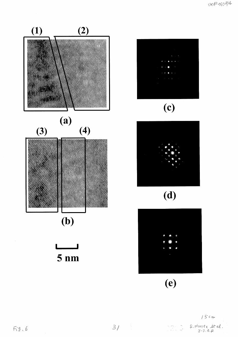
。
(c)
、‘,ノ4守/a置、
、‘,ノa
/aE‘、
、‘,ノ句
3/a
・、
(d)
、‘,ノLU
/aE‘、
5nm
(e)
ミ;イ
(c) (a)
(3) (4)
(d)
(b)
I I
5nm
(e)

10-1
N g 10田 3、、〈
〉、+-'
~ 1 O-.J
ω 。+-' c ω 吋
~ 10 ・ ιJ 。0) m よ~聞 Qg 1O d
J
10幽 11
100 nm PZT /10 nm YSZ/Si
γs出 4600C
As叩 Grown
Step叩 Annealed
-4 -2 0 2 4
Voltage (V)
3
C o
As-Grown
Step-Annealed
-4 - 2 0 2 4
Voltage (V)

12
(1/K)
810
1000庁
2 4 6 10・41
ト As-Grown 剛
幽ト
幽Applied Voltage口 3Vい
副ト
剛• • • ト O
O
O
ト
. • • • • O
O
O
ド(〈)
.
削
圃
剛
0
0
0
0
0
0
0
0
0
0
0
0
.。{・
0.。O
・C
・-
0
4
ト
さむとコO
ト
. ド
. ド
書4 置. E
500 400
(K)
300
Temperature T
200 100
1000/T
246 10-4 .. · I • • • 1 T T
~ As-Grown
(11K)
8 10 T T T • I • •
· Applied Voltage = 3V ·
• 0 • •
• •
o • o •
o • o •
12 · · · ·
·
·
·
-0000 •
· ·
· · I • I • I • I •
100 200 300 400 500
Temperature T (K)

600 '0 nm YSZ/Si , MHz
0.' V /s 500
400
300
(NEυ¥LC)
ωυcωμ
一υ向丘∞
υ
4 3 2
(V) 。しV
門ud
2u
+L o
v
O 四 2-3 -4 200
600 '0 nm YSZ/Si
, MHz .......-. 0.' V Is N
E 500 u
" W-e:
""-"
OJ 400 u e: ro +-' u ro a. 300 ro
U
200 ~~~~~~~~~~~~~~~~~~~~~~ -4 -3 - 2 - , 0 , 2 3 4
Voltage (V)

100 nm PZT /1 0 nm YSZ/Si
Ts=4600C, Step四 Annealed
1 MHz
+ 0.1V/s o 0.5V/s
1.0V/s
250
200
150
〈
Nευ¥LC)む
υcctυω立問ハ)
100 -4 6 4
(V)
O
Voltage
よ
四 2
.......... N
5 200 ""u... c
'-'"
OJ U C co
.t: 150 u co 0.. co
U
Ts=460°C, Step-Annealed 1 MHz
+ 0.1V/s o 0.5V/s
1.0V/s
100~~~~~~~~~~~~~~~~~~~~--~
-4 - 2
3
o 2
Voltage (V) 4 6

c ,-0.521 nm
0.514 nm
aggEzze
jttF
色、
m圃 PZT
YSZ
m-PZT
c '-0.521 nm
YSZ
0.514 nm
l I

• • • 001 000 001
• • • 111 110 111
• • • (a). m・1聞
1 1 0
• 100 010
• • 一 一1 1 0 000 1 1 0
• • • 一 一010 100
• • 1 1 0
• (b) m欄 PZT[001 ]
ヘイJ
-111 110 111
• • • -
001 000 001
• • • 111 110 111
• • • -
(a)· m-PZT [ 110 ]
1 1 0 • 100 010
• • - -
1 1 0 000 1 1 0 • • • - -010 100 • •
1 1 0
• (b) m-PZT [ 001 ]


![dspace.jaist.ac.jp...Japan Advanced Institute of Science and Technology JAIST Repository Title Assessment and Improvement of Security Awareness Training Methodologies [Project Paper]](https://img.pdfslide.net/doc/110x75/60e9ff58c117771a262f2d33/-japan-advanced-institute-of-science-and-technology-jaist-repository-title-assessment.jpg)