Embed Size (px)
Citation preview

SCLS315O − MARCH 1996 − REVISED JUNE 2005
1POST OFFICE BOX 655303 • DALLAS, TEXAS 75265
Operating Range of 4.5 V to 5.5 V
Max tpd of 7.1 ns at 5 V
Low Power Consumption, 10- µA Max ICC ±8-mA Output Drive at 5 V
Inputs Are TTL-Voltage Compatible
Latch-Up Performance Exceeds 250 mA PerJESD 17
3
2
4
51A VCC
Y
B
GND
DBV PACKAGE(TOP VIEW) DCK PACKAGE
(TOP VIEW)
3
2
4
51A VCC
Y
B
GND
3
2
4
51A VCC
Y
B
GND
DRL PACKAGE(TOP VIEW)
See mechanical drawings for dimensions.
description/ordering information
The SN74AHCT1G08 is a single 2-input positive-AND gate. The device performs the Boolean function
Y A • B or Y A B in positive logic.
ORDERING INFORMATION
TA PACKAGE † ORDERABLEPART NUMBER
TOP-SIDEMARKING‡
SOT (SOT-23) − DBVReel of 3000 SN74AHCT1G08DBVR
B08_SOT (SOT-23) − DBVReel of 250 SN74AHCT1G08DBVT
B08_
−40°C to 85°CSOT (SC-70) − DCK
Reel of 3000 SN74AHCT1G08DCKRBE_
−40 C to 85 CSOT (SC-70) − DCK
Reel of 250 SN74AHCT1G08DCKTBE_
SOT (SOT-553) − DRL Reel of 4000 SN74AHCT1G08DRLR BE_
† Package drawings, standard packing quantities, thermal data, symbolization, and PCB design guidelines areavailable at www.ti.com/sc/package.
‡ The actual top-side marking has one additional character that designates the assembly/test site.
FUNCTION TABLE
INPUTS OUTPUTA B
OUTPUTY
H H H
L X L
X L L
logic diagram (positive logic)
1
24A
BY
! "#$ ! %#&'" ($)(#"! " !%$""! %$ *$ $! $+! !#$!!(( ,-) (#" %"$!!. ($! $"$!!'- "'#($$!. '' %$$!)
Copyright 2005, Texas Instruments Incorporated
Please be aware that an important notice concerning availability, standard warranty, and use in critical applications ofTexas Instruments semiconductor products and disclaimers thereto appears at the end of this data sheet.
SCLS315O − MARCH 1996 − REVISED JUNE 2005
2 POST OFFICE BOX 655303 • DALLAS, TEXAS 75265
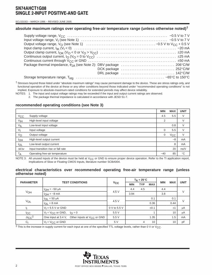
absolute maximum ratings over operating free-air temperature range (unless otherwise noted) †
Supply voltage range, VCC −0.5 V to 7 V. . . . . . . . . . . . . . . . . . . . . . . . . . . . . . . . . . . . . . . . . . . . . . . . . . . . . . . . . . Input voltage range, VI (see Note 1) −0.5 V to 7 V. . . . . . . . . . . . . . . . . . . . . . . . . . . . . . . . . . . . . . . . . . . . . . . . . . Output voltage range, VO (see Note 1) −0.5 V to VCC + 0.5 V. . . . . . . . . . . . . . . . . . . . . . . . . . . . . . . . . . . . . . . . Input clamp current, IIK (VI < 0) −20 mA. . . . . . . . . . . . . . . . . . . . . . . . . . . . . . . . . . . . . . . . . . . . . . . . . . . . . . . . . . . Output clamp current, IOK (VO < 0 or VO > VCC) ±20 mA. . . . . . . . . . . . . . . . . . . . . . . . . . . . . . . . . . . . . . . . . . . . Continuous output current, IO (VO = 0 to VCC) ±25 mA. . . . . . . . . . . . . . . . . . . . . . . . . . . . . . . . . . . . . . . . . . . . . . Continuous current through VCC or GND ±50 mA. . . . . . . . . . . . . . . . . . . . . . . . . . . . . . . . . . . . . . . . . . . . . . . . . . . Package thermal impedance, θJA (see Note 2): DBV package 206°C/W. . . . . . . . . . . . . . . . . . . . . . . . . . . . . . .
DCK package 252°C/W. . . . . . . . . . . . . . . . . . . . . . . . . . . . . . . DRL package 142°C/W. . . . . . . . . . . . . . . . . . . . . . . . . . . . . . .
Storage temperature range, Tstg −65°C to 150°C. . . . . . . . . . . . . . . . . . . . . . . . . . . . . . . . . . . . . . . . . . . . . . . . . . .
† Stresses beyond those listed under “absolute maximum ratings” may cause permanent damage to the device. These are stress ratings only, andfunctional operation of the device at these or any other conditions beyond those indicated under “recommended operating conditions” is notimplied. Exposure to absolute-maximum-rated conditions for extended periods may affect device reliability.
NOTES: 1. The input and output voltage ratings may be exceeded if the input and output current ratings are observed.2. The package thermal impedance is calculated in accordance with JESD 51-7.
recommended operating conditions (see Note 3)
MIN MAX UNIT
VCC Supply voltage 4.5 5.5 V
VIH High-level input voltage 2 V
VIL Low-level input voltage 0.8 V
VI Input voltage 0 5.5 V
VO Output voltage 0 VCC V
IOH High-level output current −8 mA
IOL Low-level output current 8 mA
∆t/∆v Input transition rise or fall rate 20 ns/V
TA Operating free-air temperature −40 85 °C
NOTE 3: All unused inputs of the device must be held at VCC or GND to ensure proper device operation. Refer to the TI application report,Implications of Slow or Floating CMOS Inputs, literature number SCBA004.
electrical characteristics over recommended operating free-air temperature range (unlessotherwise noted)
PARAMETER TEST CONDITIONS VCCTA = 25°C
MIN MAX UNITPARAMETER TEST CONDITIONS VCC MIN TYP MAXMIN MAX UNIT
VOHIOH = −50 A
4.5 V4.4 4.5 4.4
VVOH IOH = −8 mA4.5 V
3.94 3.8V
VOLIOL = 50 A
4.5 V0.1 0.1
VVOL IOL = 8 mA4.5 V
0.36 0.44V
II VI = 5.5 V or GND 0 V to 5.5 V ±0.1 ±1 A
ICC VI = VCC or GND, IO = 0 5.5 V 1 10 A
∆ICC‡ One input at 3.4 V, Other inputs at VCC or GND 5.5 V 1.35 1.5 mA
Ci VI = VCC or GND 5 V 4 10 10 pF
‡ This is the increase in supply current for each input at one of the specified TTL voltage levels, rather than 0 V or VCC.
SCLS315O − MARCH 1996 − REVISED JUNE 2005
3POST OFFICE BOX 655303 • DALLAS, TEXAS 75265
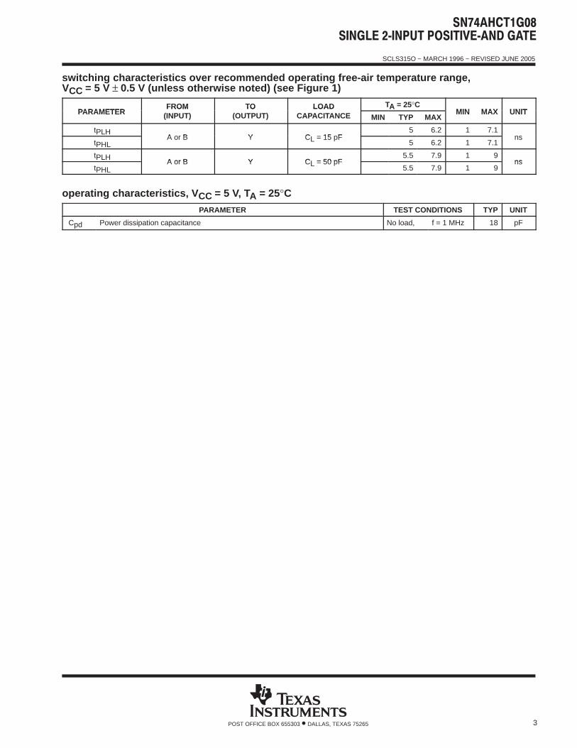
switching characteristics over recommended operating free-air temperature range, VCC = 5 V ± 0.5 V (unless otherwise noted) (see Figure 1)
PARAMETERFROM TO LOAD TA = 25°C
MIN MAX UNITPARAMETERFROM
(INPUT)TO
(OUTPUT)LOAD
CAPACITANCE MIN TYP MAXMIN MAX UNIT
tPLHA or B Y CL = 15 pF
5 6.2 1 7.1ns
tPHLA or B Y CL = 15 pF
5 6.2 1 7.1ns
tPLHA or B Y CL = 50 pF
5.5 7.9 1 9ns
tPHLA or B Y CL = 50 pF
5.5 7.9 1 9ns
operating characteristics, V CC = 5 V, TA = 25°CPARAMETER TEST CONDITIONS TYP UNIT
Cpd Power dissipation capacitance No load, f = 1 MHz 18 pF

SCLS315O − MARCH 1996 − REVISED JUNE 2005
4 POST OFFICE BOX 655303 • DALLAS, TEXAS 75265
PARAMETER MEASUREMENT INFORMATION
50% VCC
3 V
3 V
0 V
0 V
thtsu
VOLTAGE WAVEFORMSSETUP AND HOLD TIMES
Data Input
tPLH
tPHL
tPHL
tPLH
VOH
VOH
VOL
VOL
3 V
0 V
50% VCC50% VCC
Input
Out-of-PhaseOutput
In-PhaseOutput
Timing Input
50% VCC
VOLTAGE WAVEFORMSPROPAGATION DELAY TIMES
INVERTING AND NONINVERTING OUTPUTS
OutputControl
OutputWaveform 1
S1 at VCC(see Note B)
OutputWaveform 2
S1 at GND(see Note B)
VOL
VOH
tPZL
tPZH
tPLZ
tPHZ
≈VCC
0 V
50% VCC VOL + 0.3 V
50% VCC≈0 V
3 V
VOLTAGE WAVEFORMSENABLE AND DISABLE TIMES
LOW- AND HIGH-LEVEL ENABLING
tPLH/tPHLtPLZ/tPZLtPHZ/tPZHOpen Drain
OpenVCCGNDVCC
TEST S1
3 V
0 V
tw
VOLTAGE WAVEFORMSPULSE DURATION
Input
NOTES: A. CL includes probe and jig capacitance.B. Waveform 1 is for an output with internal conditions such that the output is low, except when disabled by the output control.
Waveform 2 is for an output with internal conditions such that the output is high, except when disabled by the output control.C. All input pulses are supplied by generators having the following characteristics: PRR ≤ 1 MHz, ZO = 50 Ω, tr ≤ 3 ns, tf ≤ 3 ns.D. The outputs are measured one at a time, with one input transition per measurement.E. All parameters and waveforms are not applicable to all devices.
From OutputUnder Test
CL(see Note A)
LOAD CIRCUIT FOR3-STATE AND OPEN-DRAIN OUTPUTS
S1VCC
RL = 1 kΩGND
From OutputUnder Test
CL(see Note A)
TestPoint
LOAD CIRCUIT FORTOTEM-POLE OUTPUTS
Open
VOH − 0.3 V
1.5 V 1.5 V
1.5 V
1.5 V 1.5 V
1.5 V 1.5 V1.5 V 1.5 V
Figure 1. Load Circuit and Voltage Waveforms
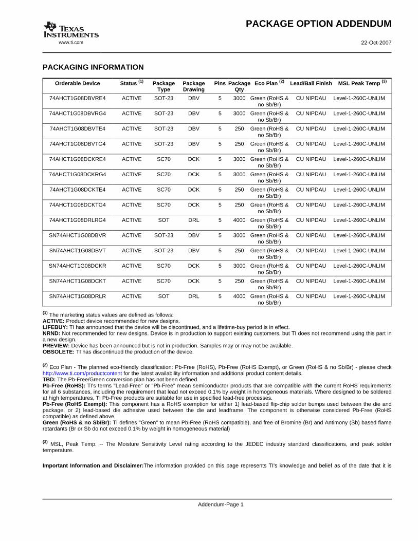
PACKAGING INFORMATION
Orderable Device Status (1) PackageType
PackageDrawing
Pins PackageQty
Eco Plan (2) Lead/Ball Finish MSL Peak Temp (3)
74AHCT1G08DBVRE4 ACTIVE SOT-23 DBV 5 3000 Green (RoHS &no Sb/Br)
CU NIPDAU Level-1-260C-UNLIM
74AHCT1G08DBVRG4 ACTIVE SOT-23 DBV 5 3000 Green (RoHS &no Sb/Br)
CU NIPDAU Level-1-260C-UNLIM
74AHCT1G08DBVTE4 ACTIVE SOT-23 DBV 5 250 Green (RoHS &no Sb/Br)
CU NIPDAU Level-1-260C-UNLIM
74AHCT1G08DBVTG4 ACTIVE SOT-23 DBV 5 250 Green (RoHS &no Sb/Br)
CU NIPDAU Level-1-260C-UNLIM
74AHCT1G08DCKRE4 ACTIVE SC70 DCK 5 3000 Green (RoHS &no Sb/Br)
CU NIPDAU Level-1-260C-UNLIM
74AHCT1G08DCKRG4 ACTIVE SC70 DCK 5 3000 Green (RoHS &no Sb/Br)
CU NIPDAU Level-1-260C-UNLIM
74AHCT1G08DCKTE4 ACTIVE SC70 DCK 5 250 Green (RoHS &no Sb/Br)
CU NIPDAU Level-1-260C-UNLIM
74AHCT1G08DCKTG4 ACTIVE SC70 DCK 5 250 Green (RoHS &no Sb/Br)
CU NIPDAU Level-1-260C-UNLIM
74AHCT1G08DRLRG4 ACTIVE SOT DRL 5 4000 Green (RoHS &no Sb/Br)
CU NIPDAU Level-1-260C-UNLIM
SN74AHCT1G08DBVR ACTIVE SOT-23 DBV 5 3000 Green (RoHS &no Sb/Br)
CU NIPDAU Level-1-260C-UNLIM
SN74AHCT1G08DBVT ACTIVE SOT-23 DBV 5 250 Green (RoHS &no Sb/Br)
CU NIPDAU Level-1-260C-UNLIM
SN74AHCT1G08DCKR ACTIVE SC70 DCK 5 3000 Green (RoHS &no Sb/Br)
CU NIPDAU Level-1-260C-UNLIM
SN74AHCT1G08DCKT ACTIVE SC70 DCK 5 250 Green (RoHS &no Sb/Br)
CU NIPDAU Level-1-260C-UNLIM
SN74AHCT1G08DRLR ACTIVE SOT DRL 5 4000 Green (RoHS &no Sb/Br)
CU NIPDAU Level-1-260C-UNLIM
(1) The marketing status values are defined as follows:ACTIVE: Product device recommended for new designs.LIFEBUY: TI has announced that the device will be discontinued, and a lifetime-buy period is in effect.NRND: Not recommended for new designs. Device is in production to support existing customers, but TI does not recommend using this part ina new design.PREVIEW: Device has been announced but is not in production. Samples may or may not be available.OBSOLETE: TI has discontinued the production of the device.
(2) Eco Plan - The planned eco-friendly classification: Pb-Free (RoHS), Pb-Free (RoHS Exempt), or Green (RoHS & no Sb/Br) - please checkhttp://www.ti.com/productcontent for the latest availability information and additional product content details.TBD: The Pb-Free/Green conversion plan has not been defined.Pb-Free (RoHS): TI's terms "Lead-Free" or "Pb-Free" mean semiconductor products that are compatible with the current RoHS requirementsfor all 6 substances, including the requirement that lead not exceed 0.1% by weight in homogeneous materials. Where designed to be solderedat high temperatures, TI Pb-Free products are suitable for use in specified lead-free processes.Pb-Free (RoHS Exempt): This component has a RoHS exemption for either 1) lead-based flip-chip solder bumps used between the die andpackage, or 2) lead-based die adhesive used between the die and leadframe. The component is otherwise considered Pb-Free (RoHScompatible) as defined above.Green (RoHS & no Sb/Br): TI defines "Green" to mean Pb-Free (RoHS compatible), and free of Bromine (Br) and Antimony (Sb) based flameretardants (Br or Sb do not exceed 0.1% by weight in homogeneous material)
(3) MSL, Peak Temp. -- The Moisture Sensitivity Level rating according to the JEDEC industry standard classifications, and peak soldertemperature.
Important Information and Disclaimer:The information provided on this page represents TI's knowledge and belief as of the date that it is
PACKAGE OPTION ADDENDUM
www.ti.com 22-Oct-2007
Addendum-Page 1

provided. TI bases its knowledge and belief on information provided by third parties, and makes no representation or warranty as to theaccuracy of such information. Efforts are underway to better integrate information from third parties. TI has taken and continues to takereasonable steps to provide representative and accurate information but may not have conducted destructive testing or chemical analysis onincoming materials and chemicals. TI and TI suppliers consider certain information to be proprietary, and thus CAS numbers and other limitedinformation may not be available for release.
In no event shall TI's liability arising out of such information exceed the total purchase price of the TI part(s) at issue in this document sold by TIto Customer on an annual basis.
PACKAGE OPTION ADDENDUM
www.ti.com 22-Oct-2007
Addendum-Page 2

TAPE AND REEL INFORMATION
*All dimensions are nominal
Device PackageType
PackageDrawing
Pins SPQ ReelDiameter
(mm)
ReelWidth
W1 (mm)
A0(mm)
B0(mm)
K0(mm)
P1(mm)
W(mm)
Pin1Quadrant
SN74AHCT1G08DBVR SOT-23 DBV 5 3000 178.0 9.2 3.3 3.2 1.55 4.0 8.0 Q3
SN74AHCT1G08DBVR SOT-23 DBV 5 3000 178.0 9.0 3.23 3.17 1.37 4.0 8.0 Q3
SN74AHCT1G08DBVR SOT-23 DBV 5 3000 180.0 9.2 3.17 3.23 1.37 4.0 8.0 Q3
SN74AHCT1G08DBVT SOT-23 DBV 5 250 178.0 9.0 3.23 3.17 1.37 4.0 8.0 Q3
SN74AHCT1G08DBVT SOT-23 DBV 5 250 180.0 9.2 3.17 3.23 1.37 4.0 8.0 Q3
SN74AHCT1G08DCKR SC70 DCK 5 3000 178.0 9.0 2.4 2.5 1.2 4.0 8.0 Q3
SN74AHCT1G08DCKR SC70 DCK 5 3000 180.0 9.2 2.3 2.55 1.2 4.0 8.0 Q3
SN74AHCT1G08DCKT SC70 DCK 5 250 178.0 9.0 2.4 2.5 1.2 4.0 8.0 Q3
SN74AHCT1G08DCKT SC70 DCK 5 250 180.0 9.2 2.3 2.55 1.2 4.0 8.0 Q3
SN74AHCT1G08DCKT SC70 DCK 5 250 178.0 9.2 2.4 2.4 1.22 4.0 8.0 Q3
SN74AHCT1G08DRLR SOT DRL 5 4000 180.0 8.4 1.98 1.78 0.69 4.0 8.0 Q3
SN74AHCT1G08DRLR SOT DRL 5 4000 180.0 9.5 1.78 1.78 0.69 4.0 8.0 Q3
PACKAGE MATERIALS INFORMATION
www.ti.com 29-Jun-2012
Pack Materials-Page 1

*All dimensions are nominal
Device Package Type Package Drawing Pins SPQ Length (mm) Width (mm) Height (mm)
SN74AHCT1G08DBVR SOT-23 DBV 5 3000 180.0 180.0 18.0
SN74AHCT1G08DBVR SOT-23 DBV 5 3000 180.0 180.0 18.0
SN74AHCT1G08DBVR SOT-23 DBV 5 3000 205.0 200.0 33.0
SN74AHCT1G08DBVT SOT-23 DBV 5 250 180.0 180.0 18.0
SN74AHCT1G08DBVT SOT-23 DBV 5 250 205.0 200.0 33.0
SN74AHCT1G08DCKR SC70 DCK 5 3000 180.0 180.0 18.0
SN74AHCT1G08DCKR SC70 DCK 5 3000 205.0 200.0 33.0
SN74AHCT1G08DCKT SC70 DCK 5 250 180.0 180.0 18.0
SN74AHCT1G08DCKT SC70 DCK 5 250 205.0 200.0 33.0
SN74AHCT1G08DCKT SC70 DCK 5 250 180.0 180.0 18.0
SN74AHCT1G08DRLR SOT DRL 5 4000 202.0 201.0 28.0
SN74AHCT1G08DRLR SOT DRL 5 4000 180.0 180.0 30.0
PACKAGE MATERIALS INFORMATION
www.ti.com 29-Jun-2012
Pack Materials-Page 2


IMPORTANT NOTICE
Texas Instruments and its subsidiaries (TI) reserve the right to make changes to their products or to discontinueany product or service without notice, and advise customers to obtain the latest version of relevant informationto verify, before placing orders, that information being relied on is current and complete. All products are soldsubject to the terms and conditions of sale supplied at the time of order acknowledgement, including thosepertaining to warranty, patent infringement, and limitation of liability.
TI warrants performance of its semiconductor products to the specifications applicable at the time of sale inaccordance with TI’s standard warranty. Testing and other quality control techniques are utilized to the extentTI deems necessary to support this warranty. Specific testing of all parameters of each device is not necessarilyperformed, except those mandated by government requirements.
CERTAIN APPLICATIONS USING SEMICONDUCTOR PRODUCTS MAY INVOLVE POTENTIAL RISKS OFDEATH, PERSONAL INJURY, OR SEVERE PROPERTY OR ENVIRONMENTAL DAMAGE (“CRITICALAPPLICATIONS”). TI SEMICONDUCTOR PRODUCTS ARE NOT DESIGNED, AUTHORIZED, ORWARRANTED TO BE SUITABLE FOR USE IN LIFE-SUPPORT DEVICES OR SYSTEMS OR OTHERCRITICAL APPLICATIONS. INCLUSION OF TI PRODUCTS IN SUCH APPLICATIONS IS UNDERSTOOD TOBE FULLY AT THE CUSTOMER’S RISK.
In order to minimize risks associated with the customer’s applications, adequate design and operatingsafeguards must be provided by the customer to minimize inherent or procedural hazards.
TI assumes no liability for applications assistance or customer product design. TI does not warrant or representthat any license, either express or implied, is granted under any patent right, copyright, mask work right, or otherintellectual property right of TI covering or relating to any combination, machine, or process in which suchsemiconductor products or services might be or are used. TI’s publication of information regarding any thirdparty’s products or services does not constitute TI’s approval, warranty or endorsement thereof.
Copyright © 1998, Texas Instruments Incorporated