Embed Size (px)
Citation preview
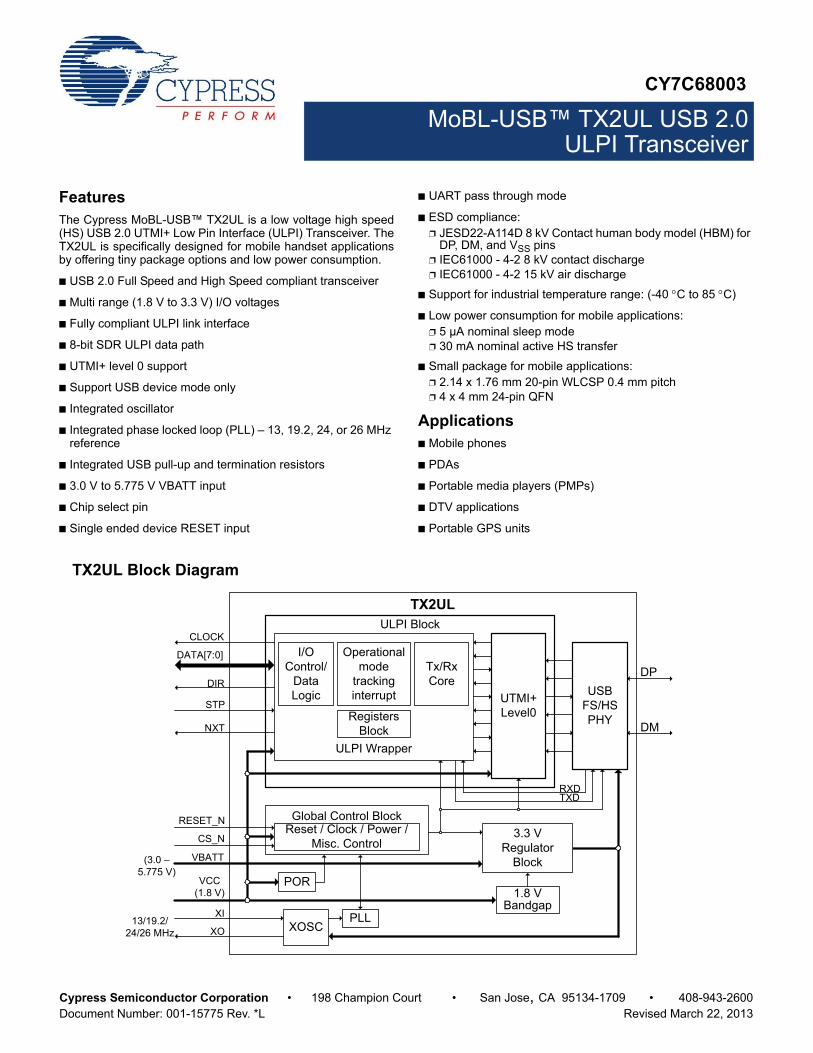
CY7C68003
MoBL-USB™ TX2UL USB 2.0ULPI Transceiver
Cypress Semiconductor Corporation • 198 Champion Court • San Jose, CA 95134-1709 • 408-943-2600Document Number: 001-15775 Rev. *L Revised March 22, 2013
FeaturesThe Cypress MoBL-USB™ TX2UL is a low voltage high speed(HS) USB 2.0 UTMI+ Low Pin Interface (ULPI) Transceiver. TheTX2UL is specifically designed for mobile handset applicationsby offering tiny package options and low power consumption.
■ USB 2.0 Full Speed and High Speed compliant transceiver
■ Multi range (1.8 V to 3.3 V) I/O voltages
■ Fully compliant ULPI link interface
■ 8-bit SDR ULPI data path
■ UTMI+ level 0 support
■ Support USB device mode only
■ Integrated oscillator
■ Integrated phase locked loop (PLL) – 13, 19.2, 24, or 26 MHz reference
■ Integrated USB pull-up and termination resistors
■ 3.0 V to 5.775 V VBATT input
■ Chip select pin
■ Single ended device RESET input
■ UART pass through mode
■ ESD compliance:❐ JESD22-A114D 8 kV Contact human body model (HBM) for
DP, DM, and VSS pins❐ IEC61000 - 4-2 8 kV contact discharge❐ IEC61000 - 4-2 15 kV air discharge
■ Support for industrial temperature range: (-40 C to 85 C)
■ Low power consumption for mobile applications:❐ 5 µA nominal sleep mode❐ 30 mA nominal active HS transfer
■ Small package for mobile applications:❐ 2.14 x 1.76 mm 20-pin WLCSP 0.4 mm pitch❐ 4 x 4 mm 24-pin QFN
Applications■ Mobile phones
■ PDAs
■ Portable media players (PMPs)
■ DTV applications
■ Portable GPS units
TX2ULULPI Block
XOSC
ULPI Wrapper
UTMI+ Level0
DATA[7:0]
CLOCK
DIR
STP
NXT
XI
XO
VBATT
13/19.2/24/26 MHz
RESET_N
DP
DM
I/O Control/
Data Logic
Operational mode
tracking interrupt
Tx/Rx Core
RegistersBlock
Global Control BlockReset / Clock / Power /
Misc. Control
POR
PLL
1.8 V Bandgap
USB FS/HS PHY
CS_N 3.3 V Regulator
Block(3.0 – 5.775 V)
VCC (1.8 V)
RXDTXD
TX2UL Block Diagram
CY7C68003
Document Number: 001-15775 Rev. *L Page 2 of 30
Contents
Functional Overview ........................................................ 3UTMI+ Low Pin Interface (ULPI) ................................. 3Oscillator (OSC) .......................................................... 3Phase Locked Loop (PLL) ........................................... 3Power On Reset (POR) ............................................... 3Reset (RESET_N) ....................................................... 3DP and DM pins .......................................................... 3Chip Select (CS_N) ..................................................... 3USB2 Transceiver Macrocell Interface (UTMI+) .......... 3Global Control ............................................................. 3Full Speed and
High Speed USB Transceivers (FS/HS) ............................. 3USB Pull up and Intr Detect,
Termination Resistors (Pull up/TERM) ............................... 3UART Pass Through Mode ......................................... 3Clocking .......................................................................4Power Domains ........................................................... 4Operation Modes .........................................................5VID and PID ................................................................ 6
Pinouts .............................................................................. 7Synchronous Operation Modes ...................................... 9
ULPI Transmit Command Byte (TX CMD) .................. 9ULPI Receive Command Byte (RX CMD) ................... 9USB Data Transmit (NOPID) ..................................... 10USB Data Transmit (PID) .......................................... 11USB Packet Receive ................................................. 11Immediate Register Read and Write ......................... 12Immediate Register Read
and Write Aborted by USB Receive ................................. 13Back to Back Immediate Register Read
and Write and USB Receive ............................................. 14
Configuration Mode ........................................................ 16Configuration Mode in 20-Pin CSP package ............. 16Configuration Mode in 24-Pin QFN package ............. 16Power On Reset (POR) ............................................. 16Register ..................................................................... 16Register Map ............................................................. 16Immediate Register Set ............................................. 17Function Control Register .......................................... 17Interface Control Register ......................................... 18Debug Register ......................................................... 18Scratch Register ........................................................ 18Carkit Control Register .............................................. 18Drive Strength and
Slew Rate Configuration Register .................................... 19USB Interface Control Register ................................. 19
Absolute Maximum Ratings .......................................... 20Operating Conditions ..................................................... 20DC Characteristics ......................................................... 21AC Characteristics ......................................................... 21Ordering Information ...................................................... 24
Ordering Code Definitions ......................................... 24Package Diagram ............................................................ 25Acronyms ........................................................................ 27Document Conventions ................................................. 27Document History Page ................................................. 28Sales, Solutions, and Legal Information ...................... 30
Worldwide Sales and Design Support ....................... 30Products .................................................................... 30PSoC Solutions ......................................................... 30
CY7C68003
Document Number: 001-15775 Rev. *L Page 3 of 30
Functional OverviewUTMI+ Low Pin Interface (ULPI)
This block conforms to the ULPI specification. It supports the8-bit wide SDR data path. The primary I/Os of this block supportmulti-range LVCMOS signaling from 1.8 V to 3.3 V (±5%). Thelevel used is automatically selected by the voltage applied toVCCIO and is set at any voltage between 1.8 V and 3.3 V.
Oscillator (OSC)
This block meets the requirements of both the on-chip PLL andthe USB-IF requirements for clock parameters. It is afundamental mode parallel resonant oscillator with a maximumESR of 60 . It supports the following:
■ Integrated Crystal Oscillator – 13, 19.2, 24, or 26 MHz crystal
■ 13, 19.2, 24, or 26 MHz LVCMOS single ended input clock on XI
Phase Locked Loop (PLL)
The PLL meets all clock stability requirements imposed by thisdevice and the USB standard. It supports all requirements tomake the device compliant to the USB 2.0 specifications. It alsohas a fractional multiplier that enables it to supply the correctfrequency to the device when it is presented with a 13, 19.2, 24,or 26 MHz reference clock.
Power On Reset (POR)
This block provides a POR signal (internal) based on the inputsupply. An internal POR is generated when VCC input risesabove VPOR(trip).
Reset (RESET_N)
The three major functions of RESET_N pin are as follows:
■ Reset TX2UL
■ Place TX2UL into Sleep Mode
■ Place TX2UL into Configuration Mode
When the RESET_N pin is asserted (low) for tSTATE (tSTATE isspecified in Table 21 on page 21), the TX2UL enters either SleepMode or Configuration Mode depending on the CS_N state.When RESET_N is asserted while CS_N is asserted, TX2ULenters Sleep Mode. When RESET_N is asserted for tSTATEwhile CS_N is deasserted, TX2UL enters Configuration Mode. Inthese modes, all the pins in the ULPI interface are tristated. If theRESET_N pin is not used, it must be pulled high. For informationabout different modes of configuration, see Table 5 on page 5.
DP and DM pins
The DP and DM pins are the differential pins for the USB. Theymust be connected to the corresponding DP and DM pins of theUSB receptacle.
Chip Select (CS_N)
This signal pin is available only in 24-pin QFN package. The twomajor functions of CS_N are as follows:
■ Tristate the ULPI bus output pins
■ Associate with RESET_N to place TX2UL in the Sleep mode
When the CS_N pin is deasserted (high), all the pins in the ULPIinterface are tristated.
USB2 Transceiver Macrocell Interface (UTMI+)
This block conforms to the UTMI+ Level 0 standard. It performsall the UTMI to USB translation.
Global Control
This block is the digital control logic that ties the blocks of thedevice together. Its functions include pull up control, over currentprotect control, and more.
Full Speed and High Speed USB Transceivers (FS/HS)
The FS and HS Transceivers comply fully with the USB 2.0specifications.
USB Pull up and Intr Detect, Termination Resistors (Pull up/TERM)
These blocks contain the USB pull-up and termination resistorsas specified by the USB 2.0 specification.
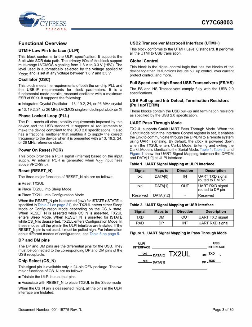
UART Pass Through Mode
TX2UL supports Carkit UART Pass Through Mode. When theCarkit Mode bit in the Interface Control register is set, it enablesthe Link to communicate through the DP/DM to a remote systemusing UART signaling. By default, the clock is powered downwhen the TX2UL enters Carkit Mode. Entering and exiting theCarkit Mode is identical to the Serial Mode. Table 1, Table 2, andFigure 1 show the UART Signal Mapping between the DP/DMand DATA[1:0] at ULPI interface.
Figure 1. UART Signal Mapping in Pass Through Mode
Table 1. UART Signal Mapping at ULPI Interface
Signal Maps to Direction Description
txd DATA[0] IN UART TXD signal routed to DM pin
rxd DATA[1] OUT UART RXD signal routed to DP pin
Reserved DATA[7:2] - Reserved
Table 2. UART Signal Mapping at USB Interface
Signal Maps to Direction Description
TXD DM OUT UART TXD signal
RXD DP INT UART RXD signal
TX2ULtxd
DP
DMDATA[0]
DATA[1]rxd
TXD
RXD
USB INTERFACE
ULPI INTERFACE
CY7C68003
Document Number: 001-15775 Rev. *L Page 4 of 30
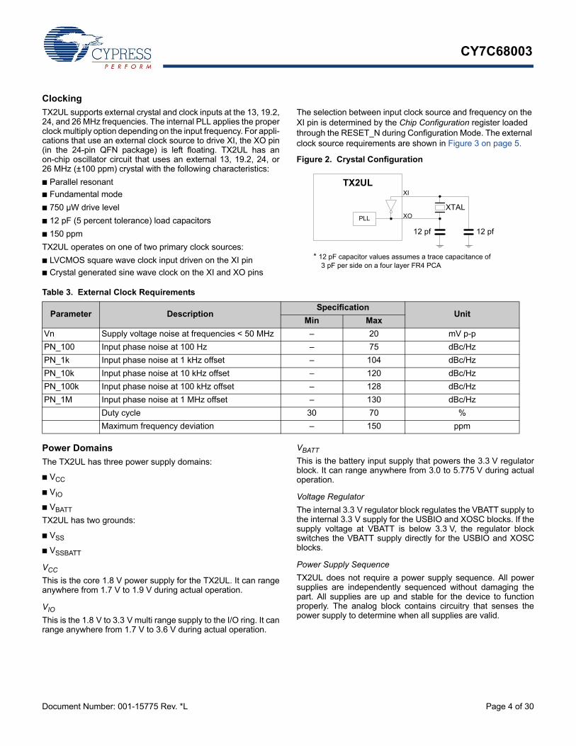
Clocking
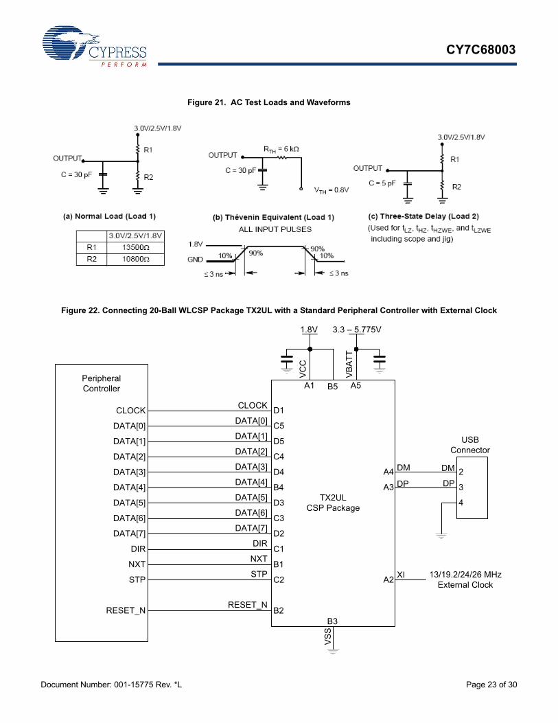
TX2UL supports external crystal and clock inputs at the 13, 19.2,24, and 26 MHz frequencies. The internal PLL applies the properclock multiply option depending on the input frequency. For appli-cations that use an external clock source to drive XI, the XO pin(in the 24-pin QFN package) is left floating. TX2UL has anon-chip oscillator circuit that uses an external 13, 19.2, 24, or26 MHz (±100 ppm) crystal with the following characteristics:
■ Parallel resonant
■ Fundamental mode
■ 750 µW drive level
■ 12 pF (5 percent tolerance) load capacitors
■ 150 ppm
TX2UL operates on one of two primary clock sources:
■ LVCMOS square wave clock input driven on the XI pin
■ Crystal generated sine wave clock on the XI and XO pins
The selection between input clock source and frequency on the XI pin is determined by the Chip Configuration register loaded through the RESET_N during Configuration Mode. The external clock source requirements are shown in Figure 3 on page 5.
Figure 2. Crystal Configuration
Power Domains
The TX2UL has three power supply domains:
■ VCC
■ VIO
■ VBATT
TX2UL has two grounds:
■ VSS
■ VSSBATT
VCC
This is the core 1.8 V power supply for the TX2UL. It can rangeanywhere from 1.7 V to 1.9 V during actual operation.
VIO
This is the 1.8 V to 3.3 V multi range supply to the I/O ring. It canrange anywhere from 1.7 V to 3.6 V during actual operation.
VBATT
This is the battery input supply that powers the 3.3 V regulatorblock. It can range anywhere from 3.0 to 5.775 V during actualoperation.
Voltage Regulator
The internal 3.3 V regulator block regulates the VBATT supply tothe internal 3.3 V supply for the USBIO and XOSC blocks. If thesupply voltage at VBATT is below 3.3 V, the regulator blockswitches the VBATT supply directly for the USBIO and XOSCblocks.
Power Supply Sequence
TX2UL does not require a power supply sequence. All powersupplies are independently sequenced without damaging thepart. All supplies are up and stable for the device to functionproperly. The analog block contains circuitry that senses thepower supply to determine when all supplies are valid.
TX2ULXI
XOPLL
12 pf 12 pf
XTAL
* 12 pF capacitor values assumes a trace capacitance of 3 pF per side on a four layer FR4 PCA
Table 3. External Clock Requirements
Parameter DescriptionSpecification
UnitMin Max
Vn Supply voltage noise at frequencies < 50 MHz – 20 mV p-p
PN_100 Input phase noise at 100 Hz – 75 dBc/Hz
PN_1k Input phase noise at 1 kHz offset – 104 dBc/Hz
PN_10k Input phase noise at 10 kHz offset – 120 dBc/Hz
PN_100k Input phase noise at 100 kHz offset – 128 dBc/Hz
PN_1M Input phase noise at 1 MHz offset – 130 dBc/Hz
Duty cycle 30 70 %
Maximum frequency deviation – 150 ppm
CY7C68003
Document Number: 001-15775 Rev. *L Page 5 of 30
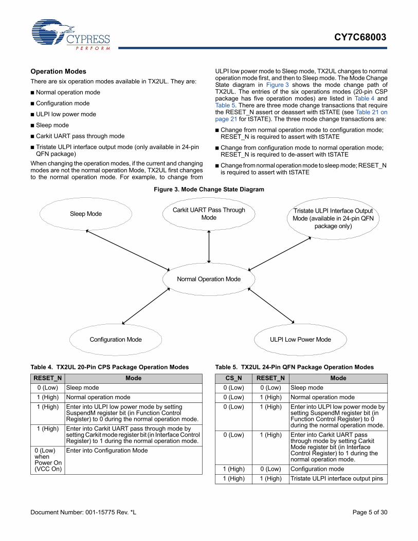
Operation Modes
There are six operation modes available in TX2UL. They are:
■ Normal operation mode
■ Configuration mode
■ ULPI low power mode
■ Sleep mode
■ Carkit UART pass through mode
■ Tristate ULPI interface output mode (only available in 24-pin QFN package)
When changing the operation modes, if the current and changingmodes are not the normal operation Mode, TX2UL first changesto the normal operation mode. For example, to change from
ULPI low power mode to Sleep mode, TX2UL changes to normaloperation mode first, and then to Sleep mode. The Mode ChangeState diagram in Figure 3 shows the mode change path ofTX2UL. The entries of the six operations modes (20-pin CSPpackage has five operation modes) are listed in Table 4 andTable 5. There are three mode change transactions that requirethe RESET_N assert or deassert with tSTATE (see Table 21 onpage 21 for tSTATE). The three mode change transactions are:
■ Change from normal operation mode to configuration mode; RESET_N is required to assert with tSTATE
■ Change from configuration mode to normal operation mode; RESET_N is required to de-assert with tSTATE
■ Change from normal operation mode to sleep mode; RESET_N is required to assert with tSTATE
Figure 3. Mode Change State Diagram
Normal Operation Mode
Tristate ULPI Interface OutputMode (available in 24-pin QFN
package only)
Sleep Mode
ULPI Low Power ModeConfiguration Mode
Carkit UART Pass Through Mode
Table 4. TX2UL 20-Pin CPS Package Operation Modes
RESET_N Mode
0 (Low) Sleep mode
1 (High) Normal operation mode
1 (High) Enter into ULPI low power mode by setting SuspendM register bit (in Function Control Register) to 0 during the normal operation mode.
1 (High) Enter into Carkit UART pass through mode by setting Carkit mode register bit (in Interface Control Register) to 1 during the normal operation mode.
0 (Low) when Power On (VCC On)
Enter into Configuration Mode
Table 5. TX2UL 24-Pin QFN Package Operation Modes
CS_N RESET_N Mode
0 (Low) 0 (Low) Sleep mode
0 (Low) 1 (High) Normal operation mode
0 (Low) 1 (High) Enter into ULPI low power mode by setting SuspendM register bit (in Function Control Register) to 0 during the normal operation mode.
0 (Low) 1 (High) Enter into Carkit UART pass through mode by setting Carkit Mode register bit (in Interface Control Register) to 1 during thenormal operation mode.
1 (High) 0 (Low) Configuration mode
1 (High) 1 (High) Tristate ULPI interface output pins
CY7C68003
Document Number: 001-15775 Rev. *L Page 6 of 30
The operation and configuration modes are described in thesections Operation Modes on page 5 and Configuration Mode onpage 16 respectively. The ULPI low power mode and Sleepmode are described in the following sections.
ULPI Low Power Mode
In this mode, the link optionally places the TX2UL in low powermode when the USB is suspended. TX2UL powers down all thecircuitry except for the interface pins and full speed receiver. Toenter low power mode, the link must set SuspendM in theFunction Control register to 0b. The TX2UL clock is stopped fora minimum of five cycles after TX2UL accepts the register write.To exit low power mode, the link signals TX2UL to exit the modeby asynchronously asserting a signal, STP. The TX2UL wakesup its internal circuitry and when it meets the ULPI timing require-ments, it deasserts DIR. The SuspendM register is set to 1b.
Sleep Mode
Sleep mode is entered by asserting RESET_N during the NormalOperation Mode. When RESET_N is driven low for tSTATE (seeTable 21 on page 21 for tSTATE requirement) while CS_N is low,TX2UL enters Sleep Mode. VCC must remain supplied (ON)during the sleep mode. This mode powers down all internalcircuitry except the RESET_N pin and the chip_config register.The ULPI interface bus is tristated.
During the Sleep Mode ensure that:
■ The ULPI interface I/Os are either floating or driven high by the link
■ DP and DM are either floating or pull to 0 V
■ Deassert RESET_N to exit the Sleep Mode
VID and PID
The VID and PID are hard coded into Product ID and Vendor ID registers (read only) as shown in Table 6.
Table 6. Immediate Register Values for VID and PID
Field Name Size (bit)Address (6 bits)
ValueRd Wr Set Clr
Vendor ID (VID) Low 8 00h - - - B4h
Vendor ID (VID) High 8 01h - - - 04h
Product ID (PID) Low 8 02h - - - 03h
Product ID (PID) High 8 03h - - - 68h
CY7C68003
Document Number: 001-15775 Rev. *L Page 7 of 30
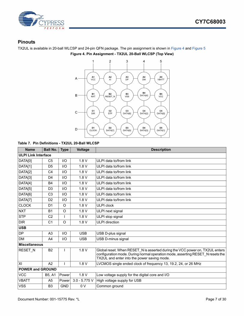
PinoutsTX2UL is available in 20-ball WLCSP and 24-pin QFN package. The pin assignment is shown in Figure 4 and Figure 5
Figure 4. Pin Assignment - TX2UL 20-Ball WLCSP (Top View)
A5VBATT
A4DM
A3DP
B2RESET_N
A2XI
C5DATA[0]
B5VCC
C3DATA[6]
B1NXT
C2STP
D5DATA[1]
D4DATA[3]
A1VCC
B3VSS
C1DIR
C4DATA[2]
B4DATA[4]
D3DATA[5]
D2DATA[7]
D1CLOCK
A
B
C
D
1 2 3 4 5
Table 7. Pin Definitions - TX2UL 20-Ball WLCSP
Name Ball No. Type Voltage Description
ULPI Link Interface
DATA[0] C5 I/O 1.8 V ULPI data to/from link
DATA[1] D5 I/O 1.8 V ULPI data to/from link
DATA[2] C4 I/O 1.8 V ULPI data to/from link
DATA[3] D4 I/O 1.8 V ULPI data to/from link
DATA[4] B4 I/O 1.8 V ULPI data to/from link
DATA[5] D3 I/O 1.8 V ULPI data to/from link
DATA[6] C3 I/O 1.8 V ULPI data to/from link
DATA[7] D2 I/O 1.8 V ULPI data to/from link
CLOCK D1 O 1.8 V ULPI clock
NXT B1 O 1.8 V ULPI next signal
STP C2 I 1.8 V ULPI stop signal
DIR C1 O 1.8 V ULPI direction
USB
DP A3 I/O USB USB D-plus signal
DM A4 I/O USB USB D-minus signal
Miscellaneous
RESET_N B2 I 1.8 V Global reset. When RESET_N is asserted during the VCC power on, TX2UL enters configuration mode. During normal operation mode, asserting RESET_N resets the TX2UL and enter into the power saving mode.
XI A2 I 1.8 V LVCMOS single ended clock of frequency 13, 19.2, 24, or 26 MHz
POWER and GROUND
VCC B5, A1 Power 1.8 V Low voltage supply for the digital core and I/O
VBATT A5 Power 3.0 - 5.775 V High voltage supply for USB
VSS B3 GND 0 V Common ground
CY7C68003
Document Number: 001-15775 Rev. *L Page 8 of 30
Figure 5. Pin Assignment - TX2UL 24-Pin QFN (Top View)
1
6
2
3
4
5
8 9 10
11
12
13
14
15
16
17
18
19
2021222324
DATA[0]
DATA[1]
DATA[2]
DA
TA
[3]
DA
TA
[4]
DA
TA
[5]
DA
TA
[6]
DATA[7]
CLOCK
DIR
STP
DP
DM
VB
AT
T
XI
XO
VC
C
RESET_N
NXT
VSSBATT
NC
VCC
VIO
CS
_N
7
TX2UL
VSS (GND)Exposed die pad
Table 8. Pin Definitions - TX2UL 24-Pin QFN
Name Pin No. Type Voltage Description
ULPI Link Interface
DATA[0] 4 I/O 1.8 - 3.3 V ULPI data to/from link
DATA[1] 5 I/O 1.8 - 3.3 V ULPI data to/from link
DATA[2] 6 I/O 1.8 - 3.3 V ULPI data to/from link
DATA[3] 8 I/O 1.8 - 3.3 V ULPI data to/from link
DATA[4] 9 I/O 1.8 - 3.3 V ULPI data to/from link
DATA[5] 11 I/O 1.8 - 3.3 V ULPI data to/from link
DATA[6] 12 I/O 1.8 - 3.3 V ULPI data to/from link
DATA[7] 13 I/O 1.8 - 3.3 V ULPI data to/from link
CLOCK 14 O 1.8 - 3.3 V ULPI clock
NXT 17 O 1.8 - 3.3 V ULPI next signal
STP 16 I 1.8 - 3.3 V ULPI stop signal
DIR 15 O 1.8 - 3.3 V ULPI direction
USB
DP 22 I/O USB USB D-plus signal
DM 23 I/O USB USB D-minus signal
Misc
CS_N 7 I 1.8 - 3.3 V When CS_N is de-asserted, all pins at ULPI interface are tristated
RESET_N 18 I 1.8 - 3.3 V Device chip global reset. When RESET_N is asserted, TX2UL is in reset and enters into the power saving mode.
XI 21 I 1.8 V Crystal or LVCMOS single ended clock of frequency 13, 19.2, 24, or 26 MHz
XO 20 O 1.8 - 3.3 V Crystal
NC 2 - - No connect
POWER and GROUND
VCC 3, 19 Power 1.8 V Low voltage supply for the digital core
VIO 10 Power 1.8 - 3.3 V Power for multi-range I/Os
VBATT 24 Power 3.0 - 5.775 V High voltage supply for USB
VSSBATT 1 GND 0 USB ground
VSS Die Paddle GND 0 Digital ground (core and I/O)
CY7C68003
Document Number: 001-15775 Rev. *L Page 9 of 30
Synchronous Operation Modes
This section describes the synchronous mode of TX2UL ULPI interface protocol.
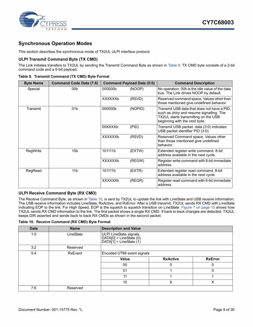
ULPI Transmit Command Byte (TX CMD)
The Link initiates transfers to TX2UL by sending the Transmit Command Byte as shown in Table 9. TX CMD byte consists of a 2-bitcommand code and a 6-bit payload.
ULPI Receive Command Byte (RX CMD)
The Receive Command Byte, as shown in Table 10, is sent by TX2UL to update the link with LineState and USB receive information.The USB receive information includes LineState, RxActive, and RxError. After a USB transmit, TX2UL sends RX CMD with LineStateindicating EOP to the link. For High Speed, EOP is the squelch to squelch transition on LineState. Figure 7 on page 10 shows howTX2UL sends RX CMD information to the link. The first packet shows a single RX CMD. If back to back changes are detected, TX2ULkeeps DIR asserted and sends back to back RX CMDs as shown in the second packet.
Table 9. Transmit Command (TX CMD) Byte Format
Byte Name Command Code Data (7:6) Command Payload Data (5:0) Command Description
Special 00b 000000b (NOOP) No operation. 00h is the idle value of the data bus. The Link drives NOOP by default.
XXXXXXb (RSVD) Reserved command space. Values other than those mentioned give undefined behavior.
Transmit 01b 000000b (NOPID) Transmit USB data that does not have a PID, such as chirp and resume signalling. The TX2UL starts transmitting on the USB beginning with the next byte.
00XXXXb (PID) Transmit USB packet. data (3:0) indicates USB packet identifier PID (3:0)
XXXXXXb (RSVD) Reserved Command space. Values other than those mentioned give undefined behavior.
RegWrite 10b 101111b (EXTW) Extended register write command. 8-bit address available in the next cycle.
XXXXXXb (REGW) Register write command with 6-bit immediate address.
RegRead 11b 101111b (EXTR) Extended register read command. 8-bit address available in the next cycle.
XXXXXXb (REGR) Register read command with 6-bit immediate address.
Table 10. Receive Command (RX CMD) Byte Format
Data Name Description and Value
1:0 LineState ULPI LineState signals.DATA[0] = LineState (0)DATA[1] = LineState (1)
3:2 Reserved
5:4 RxEvent Encoded UTMI event signals
Value RxActive RxError
00 0 0
01 1 0
11 1 1
10 X X
7:6 Reserved
CY7C68003
Document Number: 001-15775 Rev. *L Page 10 of 30
Figure 6. Sending RX CMD
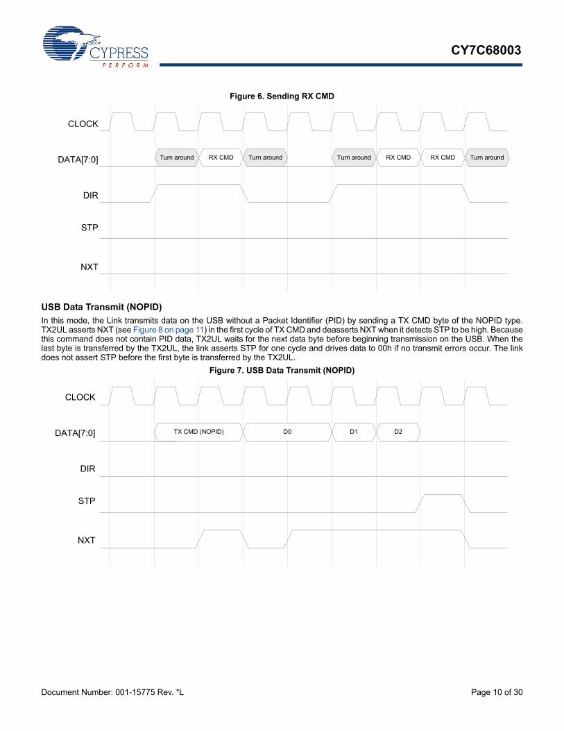
USB Data Transmit (NOPID)
In this mode, the Link transmits data on the USB without a Packet Identifier (PID) by sending a TX CMD byte of the NOPID type.TX2UL asserts NXT (see Figure 8 on page 11) in the first cycle of TX CMD and deasserts NXT when it detects STP to be high. Becausethis command does not contain PID data, TX2UL waits for the next data byte before beginning transmission on the USB. When thelast byte is transferred by the TX2UL, the link asserts STP for one cycle and drives data to 00h if no transmit errors occur. The linkdoes not assert STP before the first byte is transferred by the TX2UL.
Figure 7. USB Data Transmit (NOPID)
CLOCK
DATA[7:0]
DIR
STP
NXT
Turn around RX CMD Turn around Turn around RX CMD RX CMD Turn around
D1
CLOCK
DATA[7:0]
DIR
STP
NXT
D0TX CMD (NOPID) D2
CY7C68003
Document Number: 001-15775 Rev. *L Page 11 of 30
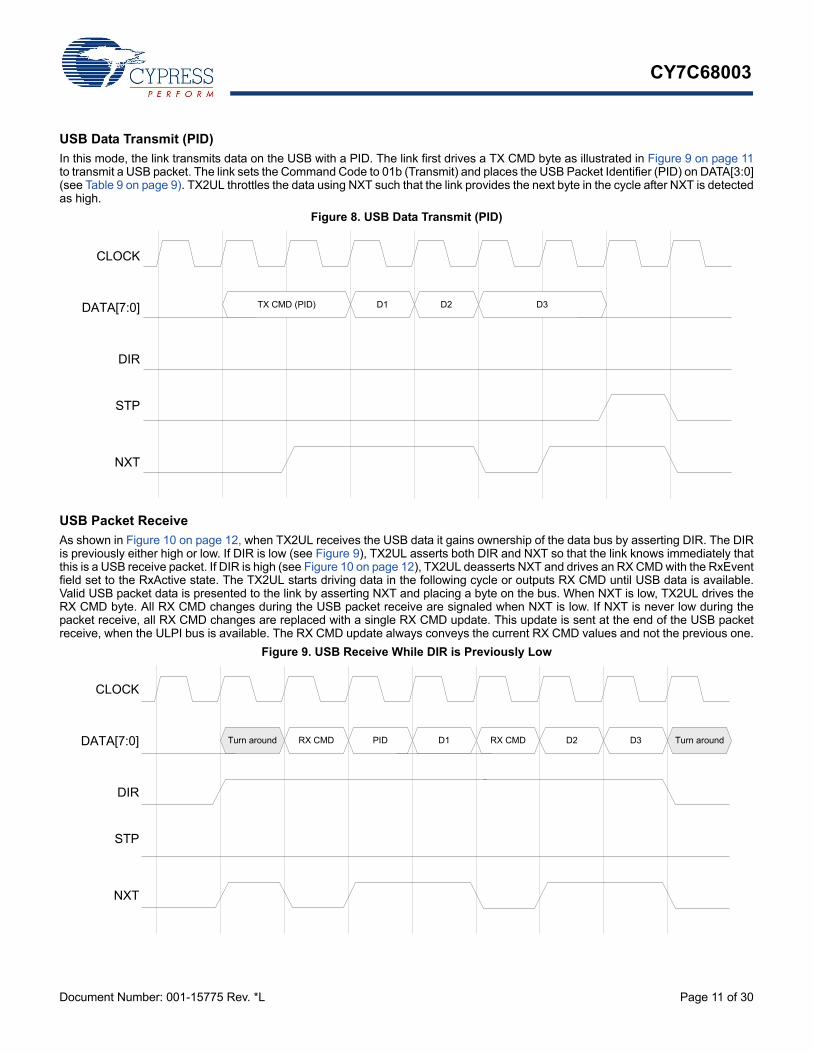
USB Data Transmit (PID)
In this mode, the link transmits data on the USB with a PID. The link first drives a TX CMD byte as illustrated in Figure 9 on page 11to transmit a USB packet. The link sets the Command Code to 01b (Transmit) and places the USB Packet Identifier (PID) on DATA[3:0](see Table 9 on page 9). TX2UL throttles the data using NXT such that the link provides the next byte in the cycle after NXT is detectedas high.
Figure 8. USB Data Transmit (PID)
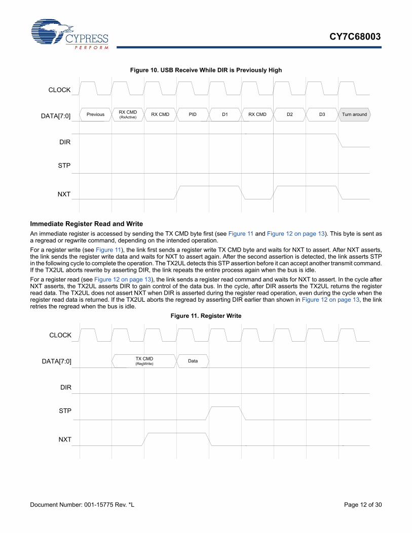
USB Packet Receive
As shown in Figure 10 on page 12, when TX2UL receives the USB data it gains ownership of the data bus by asserting DIR. The DIRis previously either high or low. If DIR is low (see Figure 9), TX2UL asserts both DIR and NXT so that the link knows immediately thatthis is a USB receive packet. If DIR is high (see Figure 10 on page 12), TX2UL deasserts NXT and drives an RX CMD with the RxEventfield set to the RxActive state. The TX2UL starts driving data in the following cycle or outputs RX CMD until USB data is available.Valid USB packet data is presented to the link by asserting NXT and placing a byte on the bus. When NXT is low, TX2UL drives theRX CMD byte. All RX CMD changes during the USB packet receive are signaled when NXT is low. If NXT is never low during thepacket receive, all RX CMD changes are replaced with a single RX CMD update. This update is sent at the end of the USB packetreceive, when the ULPI bus is available. The RX CMD update always conveys the current RX CMD values and not the previous one.
Figure 9. USB Receive While DIR is Previously Low
CLOCK
DATA[7:0]
DIR
STP
NXT
D1TX CMD (PID) D2 D3
CLOCK
DATA[7:0]
DIR
STP
NXT
Turn around RX CMD PID D1 RX CMD D2 D3 Turn around
CY7C68003
Document Number: 001-15775 Rev. *L Page 12 of 30
Figure 10. USB Receive While DIR is Previously High
Immediate Register Read and Write
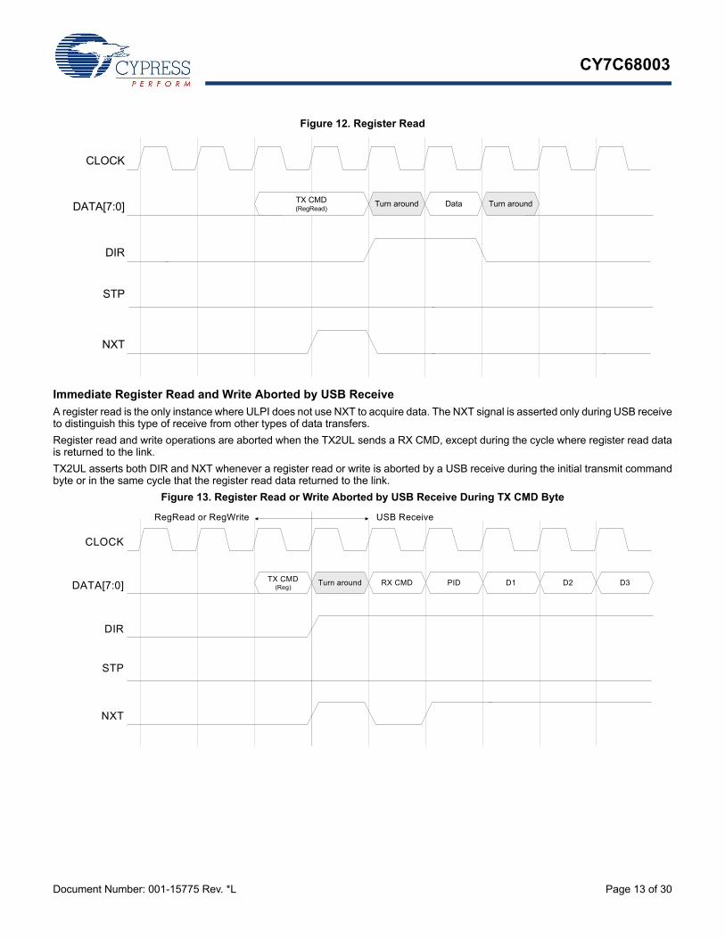
An immediate register is accessed by sending the TX CMD byte first (see Figure 11 and Figure 12 on page 13). This byte is sent asa regread or regwrite command, depending on the intended operation.
For a register write (see Figure 11), the link first sends a register write TX CMD byte and waits for NXT to assert. After NXT asserts,the link sends the register write data and waits for NXT to assert again. After the second assertion is detected, the link asserts STPin the following cycle to complete the operation. The TX2UL detects this STP assertion before it can accept another transmit command.If the TX2UL aborts rewrite by asserting DIR, the link repeats the entire process again when the bus is idle.
For a register read (see Figure 12 on page 13), the link sends a register read command and waits for NXT to assert. In the cycle afterNXT asserts, the TX2UL asserts DIR to gain control of the data bus. In the cycle, after DIR asserts the TX2UL returns the registerread data. The TX2UL does not assert NXT when DIR is asserted during the register read operation, even during the cycle when theregister read data is returned. If the TX2UL aborts the regread by asserting DIR earlier than shown in Figure 12 on page 13, the linkretries the regread when the bus is idle.
Figure 11. Register Write
CLOCK
DATA[7:0]
DIR
STP
NXT
RX CMD PIDPrevious RX CMD(RxActive)
D1 RX CMD D2 D3 Turn around
CLOCK
DATA[7:0]
DIR
STP
NXT
DataTX CMD(RegWrite)
CY7C68003
Document Number: 001-15775 Rev. *L Page 13 of 30
Figure 12. Register Read
Immediate Register Read and Write Aborted by USB Receive
A register read is the only instance where ULPI does not use NXT to acquire data. The NXT signal is asserted only during USB receiveto distinguish this type of receive from other types of data transfers.
Register read and write operations are aborted when the TX2UL sends a RX CMD, except during the cycle where register read datais returned to the link.
TX2UL asserts both DIR and NXT whenever a register read or write is aborted by a USB receive during the initial transmit commandbyte or in the same cycle that the register read data returned to the link.
Figure 13. Register Read or Write Aborted by USB Receive During TX CMD Byte
CLOCK
DATA[7:0]
DIR
STP
NXT
Turn aroundTX CMD(RegRead)
Data Turn around
CLOCK
DATA[7:0]
DIR
STP
NXT
RegRead or RegWrite USB Receive
TX CMD(Reg)
Turn around RX CMD PID D1 D2 D3
CY7C68003
Document Number: 001-15775 Rev. *L Page 14 of 30
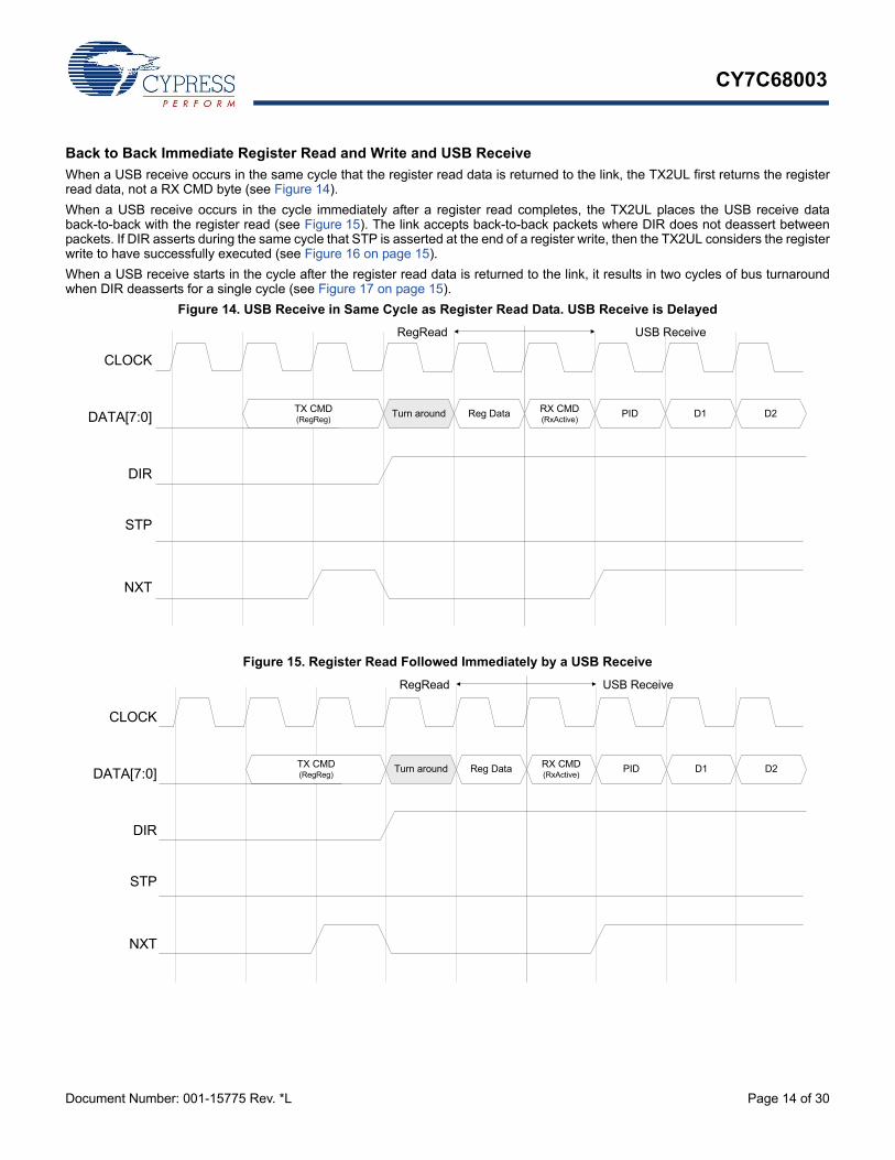
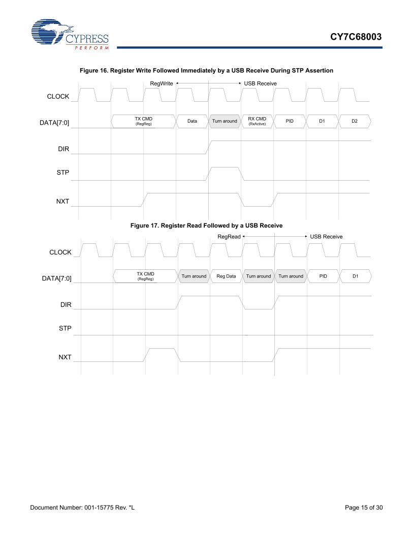
Back to Back Immediate Register Read and Write and USB Receive
When a USB receive occurs in the same cycle that the register read data is returned to the link, the TX2UL first returns the registerread data, not a RX CMD byte (see Figure 14).
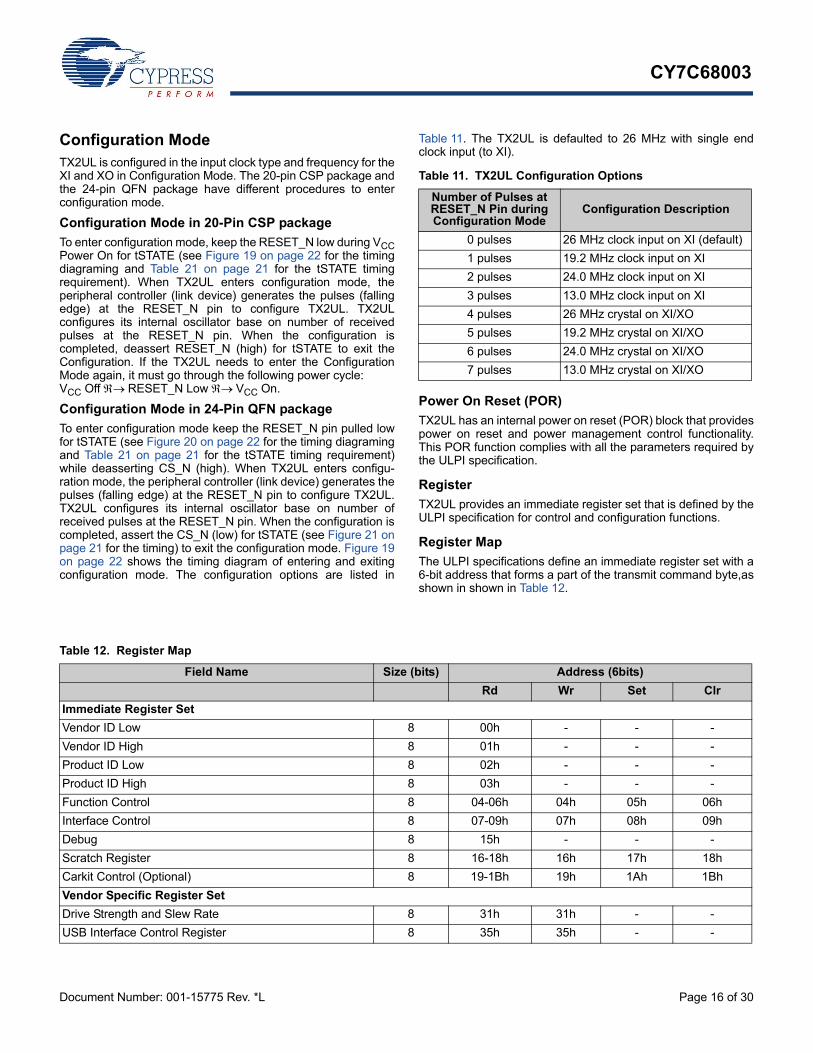
When a USB receive occurs in the cycle immediately after a register read completes, the TX2UL places the USB receive databack-to-back with the register read (see Figure 15). The link accepts back-to-back packets where DIR does not deassert betweenpackets. If DIR asserts during the same cycle that STP is asserted at the end of a register write, then the TX2UL considers the registerwrite to have successfully executed (see Figure 16 on page 15).
When a USB receive starts in the cycle after the register read data is returned to the link, it results in two cycles of bus turnaroundwhen DIR deasserts for a single cycle (see Figure 17 on page 15).
Figure 14. USB Receive in Same Cycle as Register Read Data. USB Receive is Delayed
Figure 15. Register Read Followed Immediately by a USB Receive
CLOCK
DATA[7:0]
DIR
STP
NXT
RegRead USB Receive
Turn aroundTX CMD(RegReg)
Reg Data RX CMD(RxActive)
PID D1 D2
Turn aroundTX CMD(RegReg)
Reg Data RX CMD(RxActive)
PID D1 D2
CLOCK
DATA[7:0]
DIR
STP
NXT
RegRead USB Receive
CY7C68003
Document Number: 001-15775 Rev. *L Page 15 of 30
Figure 16. Register Write Followed Immediately by a USB Receive During STP Assertion
Figure 17. Register Read Followed by a USB Receive
CLOCK
DATA[7:0]
DIR
STP
NXT
RegWrite USB Receive
Turn aroundTX CMD(RegReg)
Data RX CMD(RxActive)
PID D1 D2
Turn aroundTX CMD(RegReg)
Reg Data PID D1
CLOCK
DATA[7:0]
DIR
STP
NXT
RegRead USB Receive
Turn around Turn around
CY7C68003
Document Number: 001-15775 Rev. *L Page 16 of 30
Configuration ModeTX2UL is configured in the input clock type and frequency for theXI and XO in Configuration Mode. The 20-pin CSP package andthe 24-pin QFN package have different procedures to enterconfiguration mode.
Configuration Mode in 20-Pin CSP package
To enter configuration mode, keep the RESET_N low during VCCPower On for tSTATE (see Figure 19 on page 22 for the timingdiagraming and Table 21 on page 21 for the tSTATE timingrequirement). When TX2UL enters configuration mode, theperipheral controller (link device) generates the pulses (fallingedge) at the RESET_N pin to configure TX2UL. TX2ULconfigures its internal oscillator base on number of receivedpulses at the RESET_N pin. When the configuration iscompleted, deassert RESET_N (high) for tSTATE to exit theConfiguration. If the TX2UL needs to enter the ConfigurationMode again, it must go through the following power cycle:VCC Off RESET_N Low VCC On.
Configuration Mode in 24-Pin QFN package
To enter configuration mode keep the RESET_N pin pulled lowfor tSTATE (see Figure 20 on page 22 for the timing diagramingand Table 21 on page 21 for the tSTATE timing requirement)while deasserting CS_N (high). When TX2UL enters configu-ration mode, the peripheral controller (link device) generates thepulses (falling edge) at the RESET_N pin to configure TX2UL.TX2UL configures its internal oscillator base on number ofreceived pulses at the RESET_N pin. When the configuration iscompleted, assert the CS_N (low) for tSTATE (see Figure 21 onpage 21 for the timing) to exit the configuration mode. Figure 19on page 22 shows the timing diagram of entering and exitingconfiguration mode. The configuration options are listed in
Table 11. The TX2UL is defaulted to 26 MHz with single endclock input (to XI).
Power On Reset (POR)
TX2UL has an internal power on reset (POR) block that providespower on reset and power management control functionality.This POR function complies with all the parameters required bythe ULPI specification.
Register
TX2UL provides an immediate register set that is defined by theULPI specification for control and configuration functions.
Register Map
The ULPI specifications define an immediate register set with a6-bit address that forms a part of the transmit command byte,asshown in shown in Table 12.
Table 11. TX2UL Configuration Options
Number of Pulses at RESET_N Pin during Configuration Mode
Configuration Description
0 pulses 26 MHz clock input on XI (default)
1 pulses 19.2 MHz clock input on XI
2 pulses 24.0 MHz clock input on XI
3 pulses 13.0 MHz clock input on XI
4 pulses 26 MHz crystal on XI/XO
5 pulses 19.2 MHz crystal on XI/XO
6 pulses 24.0 MHz crystal on XI/XO
7 pulses 13.0 MHz crystal on XI/XO
Table 12. Register Map
Field Name Size (bits) Address (6bits)
Rd Wr Set Clr
Immediate Register Set
Vendor ID Low 8 00h - - -
Vendor ID High 8 01h - - -
Product ID Low 8 02h - - -
Product ID High 8 03h - - -
Function Control 8 04-06h 04h 05h 06h
Interface Control 8 07-09h 07h 08h 09h
Debug 8 15h - - -
Scratch Register 8 16-18h 16h 17h 18h
Carkit Control (Optional) 8 19-1Bh 19h 1Ah 1Bh
Vendor Specific Register Set
Drive Strength and Slew Rate 8 31h 31h - -
USB Interface Control Register 8 35h 35h - -
CY7C68003
Document Number: 001-15775 Rev. *L Page 17 of 30
Table 13 to Table 17 on page 18 define the read, write, set, and clear register options. The following are the conventions:
■ Rd or rd = Read
■ Wr or wr = Write
■ Set or s = Set
■ Clr or c = Clear
Immediate Register Set
The details of all immediate registers of TX2UL are shown in Table 6 on page 6, Table 18 on page 19, and Table 20 on page 21.
Function Control Register
Control ULPI Function Setting of TX2UL
Table 13. Function Control Register (Address: 04h - 06h [read], 04h [write], 05h [set], 06h [clear])
Bit Field Name Description Access Reset Value
1:0 XcvrSelect Selects the required transceiver speed.00b: Enable HS transceiver01b: Enable FS transceiver10b: Reserved11b: Enable FS transceiver for LS packets.
rd/wr/s/c 01b
2 TermSelect Controls the internal 1.5 K pull up resistor and 45 HS terminations. rd/wr/s/c 0b
4:3 OpMode Selects the required bit encording style during transmit.00b: Normal operation01b: Non-driving10b: Disable bit stuff and NRZI encoding11b: Do not automatically add SYNC and EOP when transmitting. It is used only for HS packets.
rd/wr/s/c 00b
5 Reset Active high transceiver reset. After the link sets this bit, TX2UL asserts DIR and resets ULPI core. When the reset is completed, DIR is de-asserted and automatically clears this bit. After de-asserting DIR, TX2UL re-asserts DIR and sends and RX CMD update to the link. The link waits for DIR to de-assert before using ULPI bus. It does not reset the ULPI interface or ULPI register set.
rd/wr/s/c 0b
6 SuspendM Active low. Put TX2UL into Low Power Mode. TX2UL powers down all blocks except the full speed receiver and ULPI interface pins. TX2UL sets this bit to ‘1’ when it exits from low power mode.0b: Enter into low power mode1b: Normal operation mode
rd/wr/s/c 1b
7 Reserved rd x
CY7C68003
Document Number: 001-15775 Rev. *L Page 18 of 30
Interface Control Register
This register enables alternative interface and TX2UL features.
Debug Register
This register indicates the current value of various signals useful for debugging.
Scratch Register
This register is for testing purpose only. The link can read, write, set and clear this register.
Carkit Control Register
This register controls the TXD and RXD in carkit UART pass through mode. It has no control function if the CarkitMode bit in InterfaceControl Register is not set.
Table 14. Interface Control Register (Address: 07h - 09h [read], 07h [write], 08h [set], 09h [clear])
Bit Field Name Description Access Reset Value
1:0 Reserved rd xxb
2 CarkitMode Changes the ULPI interface to carkit interface that support UART pass through mode. This bit is cleared when it exits from carkit UART pass through mode.0b: Disable serial carkit mode1b: Enable serial carkit mode
rd/wr/s/c 0b
6:3 Reserved rd xxxxb
7 Interface Protect Disable
Controls circuitry built into TX2UL for protecting the ULPI interface when the link tristates STP and DATA[7:0]. Any pull ups or pull downs employed by this feature are disabled0b: Enable the interface Protect Circuit1b: Disable the Interface Protect Circuit
rd/wr/s/c 0b
Table 15. Debug Register (Address: 15h [read only])
Bit Field Name Description Access Reset Value
0 LineState0 Contains the current value of LineState(0) rd 0b
1 LineState1 Contains the current value of LineState(1) rd 0b
7:2 Reserved rd 000000b
Table 16. Scratch Register (Address: 16h - 18h [read], 16h [write], 17h [set], 18h [clear])
Bit Field Name Description Access Reset Value
7:0 Scratch Empty register byte for testing purposes. The link software reads, writes, sets, and clears this register.
rd/wr/s/c 00000000b
Table 17. Carkit Control Register (Address: 19h - 1Bh [read], 19h [write], 1Ah [set], 1Bh [clear])
Bit Field Name Description Access Reset Value
1:0 Reserved rd xxb
2 TxdEn Routes TXD signal from DATA[0] pin to DM pin rd/wr/s/c 0b
3 RxdEn Routes RXD signal from DP pin to DATA[1] pin rd/wr/s/c 0b
7:4 Reserved rd xxxxb
CY7C68003
Document Number: 001-15775 Rev. *L Page 19 of 30
Drive Strength and Slew Rate Configuration Register
This register is mapped to the vendor specific registers address. This register configures the drive strength and slew rate of the outputs.
USB Interface Control Register
This register is mapped to the vendor specific registers address. This register enables or disables the USB interface.
Table 18. Drive Strength and Slew Rate Configuration Register (Address: 31h [read], 31h [write])
Bit Field Name Description Access Reset Value
1:0 DriveStrength Configure the drive strength on the output pins00b: Full drive strength01b: Three quarter drive strength10b: half drive strength11b: Quarter drive strength
rd/wr 00b
2 SlewRate Configure the slew rate on the output pins0b: slow slew rate1b: fast slew rate
rd/wr 0b
7:3 Reserved rd 00000b
Table 19. USB Interface Control Register (Address: 35h [read], 35h [write])
Bit Field Name Description Access Reset Value
1:0 Reserved When write to this register, this field must be filled in 0s rd 00b
2 UsbEnable USB interface control0b: Disable USB interface1b: Enable USB interface
rd/wr 0b
7:3 Reserved When write to this register, this field must be filled in 0s rd 00000b
CY7C68003
Document Number: 001-15775 Rev. *L Page 20 of 30
Absolute Maximum Ratings
Exceeding maximum ratings may shorten the useful life of thedevice. User guidelines are not tested.
Storage temperature................................. –65 C to +150 C
Ambient temperature with power supplied (Industrial) ......................... –40 C to +85 C
Supply voltage to ground potential
VCC ...............................................................–0.5 V to +2.0 V
VIO ................................................................–0.5 V to +4.0 V
VBATT ........................................................–0.5 V to +5.775 V
DC input voltage to any input pin....................1.89 V to 3.6 V
Depends on I/O supply voltage. Inputs are not over voltagetolerant.
DC voltage applied to outputs in high Z state ........................ –0.5 V to VCC + 0.5 V
Static discharge voltage (ESD) from JESD22-A114.................................................. > 2000 V
Latch up current...................................................... > 200 mA
Maximum output short circuit current for all I/O configurations. (Vout = 0 V) ..................... –100 mA
Operating Conditions
Ambient temperature under bias (TA) Industrial ..................................................... –40 C to +85 C
VCC supply voltage ...........................................1.7 V to 1.9 V
VIO supply voltage ............................................1.7 V to 3.6 V
VBATT supply voltage ....................................3.0 V to 5.775 V
CY7C68003
Document Number: 001-15775 Rev. *L Page 21 of 30
DC Characteristics
AC Characteristics
Table 20. DC Specifications for All Voltage Supplies
Parameter Description Conditions Min Typ Max Unit
VCC Core voltage supply 1.7 1.8 1.9 V
VIO ULPI interface I/O voltage supply (this I/O supply is not available on 20-Ball WLCSP package)
1.7 1.8, 2.5, 3.3
3.6 V
VBATT Crystal voltage supply 3.0 – 5.775 V
VPOR(trip) Power on reset trip voltage 1.0 – 1.5 V
VIH1 Input HIGH voltage 1 All ports except USB, 2.0 V < VIO < 3.6 V
0.625 × VIO – VIO + 0.3 V
VIH2 Input HIGH voltage 2 All ports except USB,1.7 V < VIO < 2.0 V
VIO‚ 0.4 – VIO + 0.3 V
VIL Input LOW voltage –0.3 – 0.25 × VIO V
VOH Output HIGH voltage IOH(MAX) = 0.1 mA 0.9 × VIO – – V
VOL Output LOW voltage IOL(MIN) = 0.1 mA – – 0.1 × VIO V
IIX Input leakage current All I/O signals held at VDDQ 1 – 1 A
IOZ Output leakage current All I/O signals held at VDDQ 1 – 1 A
ICC Supply current Continuous Receive – 30 65 mA
Continuous Transmit – 30 65 mA
ULPI Low Power Mode (Suspend)VCC = 1.8 V
– 300 750 A
Sleep Mode- ULPI interface bus is either Hz or drive High- DP and DM must be Hz or pull low
– 5 40 A
IPU Pull up current Interface protect enabled;STP pin only; VI = 0 V
–13 – –80 A
IPD Pull down current Interface protect enabled;DATA[7:0] only;VI = VIO
16 – 90 A
Table 21. ULPI Timing Parameters
Parameter Description Min Max Unit
tCS Setup time for control input 5.8 – ns
tDS Setup time for data input 5.8 – ns
tCH Hold time for control input 0 – ns
tDH Hold time for data input 0 – ns
tCD Output delay time for control output 7.6 9.0 ns
tDD Output delay time for data output 7.6 9.0 ns
tSTATE Mode state change time 500 – s
tPW Pulse width 200 10000 ns
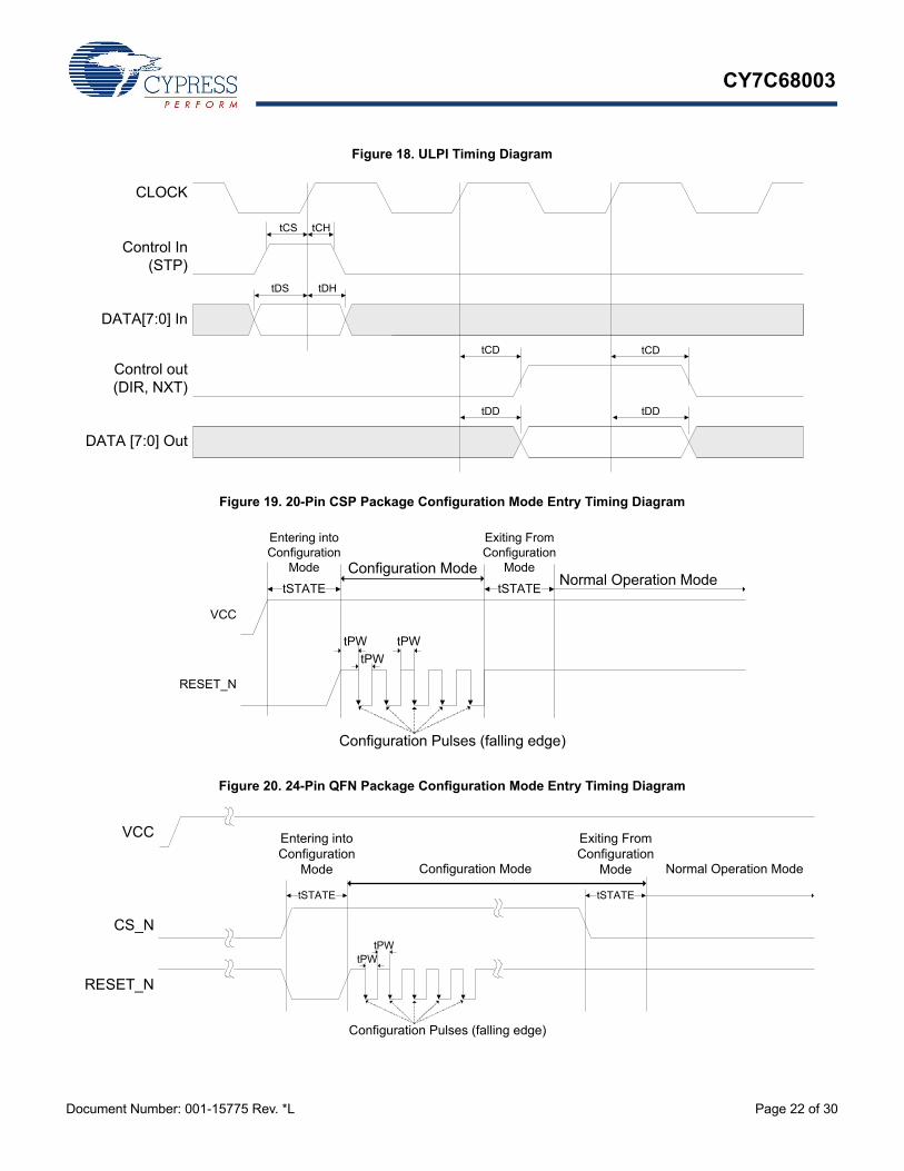
CY7C68003
Document Number: 001-15775 Rev. *L Page 22 of 30
Figure 18. ULPI Timing Diagram
Figure 19. 20-Pin CSP Package Configuration Mode Entry Timing Diagram
Figure 20. 24-Pin QFN Package Configuration Mode Entry Timing Diagram
CLOCK
Control In (STP)
DATA[7:0] In
tCS tCH
Control out (DIR, NXT)
tDS tDH
tCD tCD
DATA [7:0] Out
tDD tDD
VCC
RESET_N
Normal Operation ModetSTATE
Configuration Mode
Entering into Configuration
Mode
tSTATE
Exiting From Configuration
Mode
Configuration Pulses (falling edge)
tPW
tPW
tPW
VCC
CS_N
RESET_N
Normal Operation Mode
tSTATE
Configuration Mode
Entering into Configuration
Mode
tSTATE
Exiting From Configuration
Mode
Configuration Pulses (falling edge)
tPWtPW
CY7C68003
Document Number: 001-15775 Rev. *L Page 23 of 30
Figure 22. Connecting 20-Ball WLCSP Package TX2UL with a Standard Peripheral Controller with External Clock
Figure 21. AC Test Loads and Waveforms
DATA[0]
DATA[1]
DATA[2]
DATA[3]
DATA[4]
DATA[5]
DATA[6]
DATA[7]
DATA[0]
DATA[1]
DATA[2]
DATA[3]
DATA[4]
DATA[5]
DATA[6]
DATA[7]
CLOCKCLOCK
DIR
NXT
STP
RESET_N
VS
S
DM
DP
DM
DP
DIR
NXT
STP
RESET_N
VB
AT
T
VC
C
1.8V 3.3 – 5.775V
2
3
4
USB Connector
B3
A5
C5
D5
C4
A4D4
B4 A3
C3
A1
D3
B2
B1
D2
A2C2
C1
D1
XI 13/19.2/24/26 MHzExternal Clock
TX2ULCSP Package
Peripheral Controller B5
CY7C68003
Document Number: 001-15775 Rev. *L Page 24 of 30
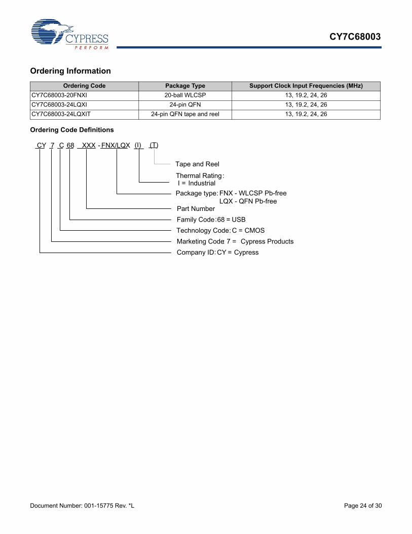
Ordering Information
Ordering Code Definitions
Ordering Code Package Type Support Clock Input Frequencies (MHz)
CY7C68003-20FNXI 20-ball WLCSP 13, 19.2, 24, 26
CY7C68003-24LQXI 24-pin QFN 13, 19.2, 24, 26
CY7C68003-24LQXIT 24-pin QFN tape and reel 13, 19.2, 24, 26
CY
Marketing Code: 7 = Cypress Products
7 C 68
Technology Code: C = CMOS
Company ID: CY = Cypress
XXX
Family Code: 68 = USB
Part Number
- FNX/LQX
Package type: FNX - WLCSP Pb-freeLQX - QFN Pb-free
(I)
Thermal Rating:I = Industrial
(T)
Tape and Reel
CY7C68003
Document Number: 001-15775 Rev. *L Page 25 of 30
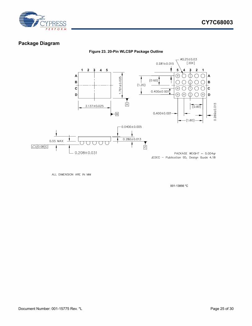
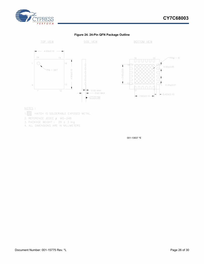
Package Diagram
Figure 23. 20-Pin WLCSP Package Outline
001-13856 *C
CY7C68003
Document Number: 001-15775 Rev. *L Page 26 of 30
Figure 24. 24-Pin QFN Package Outline
001-13937 *E
CY7C68003
Document Number: 001-15775 Rev. *L Page 27 of 30
Acronyms Document Conventions
Units of MeasureTable 22. Acronyms Used in this Document
Acronym Description
ASIC application specific integrated circuit
CPU central processing unit
DID device identifier
DSP digital signal processor
EEPROM electrically erasable programmable read only memory
EPP enhanced parallel port
ECC error correction code
FIFO first in first out
GPIF general programmable interface
GPIO general purpose input / output
HBM human body model
I/O input output
PDA personal digital assistant
PLL phase lock loop
PID product identifier
SIE serial interface engine
SOF start of frame
USB universal serial bus
VID vendor identifier
WLCSP wafer level chip scale package
ULPI UTMI+ low pin interface
Table 23. Units of Measure
Symbol Unit of Measure
KHz kilohertz
Mbytes megabytes
MHz megahertz
µA microampere
µs microseconds
µW microwatts
mA milliampere
mW milliwatts
ns nanoseconds
ppm parts per million
pF picofarads
V volts
CY7C68003
Document Number: 001-15775 Rev. *L Page 28 of 30
Document History Page
Document Title: CY7C68003 MoBL-USB™ TX2UL USB 2.0 ULPI TransceiverDocument Number: 001-15775
Revision ECN Orig. of Change Submission Date Description of Change
** 1094246 VSO, XVA See ECN Initial Release
*A 1188703 VSO See ECN Update the tSTATE min requirement (from 200 us to 500us) in Table 21Section Sleep Mode add (see Table 21 for tSTATE requirement)Section of Operating Conditions (page 19), the second VCC corrected to VIO.Table 19, the reference voltage for the VIH1, VIH2, VIL, VOH, and VOL has corrected from VCC to VIO.
*B 1505863 VSO/AESA See ECN Change in Ordering Information.
*C 2081867 VSO/AESA See ECN Update the ESD description in the features list.Updated the description of section “Power Supply Sequence”Updated the section of Chip Section (CS_N)Updated the section of Operation Modes - tri-state mode only available in 24-pin QFN packageUpdated Figure 3.Added Table 4.Updated Figure 4 and Table 7 (CSP pin assignment has been changed)Updated the section of Configuration ModeCorrect the hyper link section of Immediate Register SetCorrect the word of “Reserved” in Table 14Updated ULPI Timing Parameters table (table-21)Updated ULPI Timing Diagram (figure 18)Added Figure 19.Removed USB Interface Control Register section and table in page 19Updated Figure 22.
*D 2552066 VSO 08/13/2008 In the first page, feature list, update the CSP dimension from “2.2 x 1.8 mm” to “2.14 x 1.76 mm”.Updated Table 12Add USB Interface Control Register section
*E 2597682 VSO/AESA 10/28/2008 Removed PRELIMINARY in master pages (turn into Final data sheet).Updated data sheet template.Updated Ordering Information table.In the Clocking section, added a bullet ‘150 ppm’.Table 3:
❐ changed PN_DC to PN_100❐ changed DC to 100❐ change the unit of dB to dBc/Hz❐ added a row of ‚ÄúMaximum Frequency Devia-
tion”
*F 2671871 VSO/PYRS 03/13/2009 Updated Suspend current in Table 20 (clarified VCC = 1.8 V).Changed all TX3, TX3LP18 to TX2UL
*G 2765711 TIK/RADH 09/18/2009 Posting to external web.
*H 2920278 VSO/AESA 04/21/2010 Added “Suport USB Device Mode only” in the Feature section. Added table of conetnts.Updated links in Sales, Solutions, and Legal Information.
CY7C68003
Document Number: 001-15775 Rev. *L Page 29 of 30
*I 3035786 HBM 09/22/2010 Post to external web.
*J 3305013 ODC 07/07/2011 Corrected crystal drive level requirement.Corrected VIL min value.Format updates based on the template and style guide.Added ordering code definition diagram.Added acronyms and units of measure tables.
*K 3493857 VSO 01/17/2012 No change.
*L 3941477 KHIG 03/22/2013 Updated Absolute Maximum Ratings.
Updated Package Diagram:spec 001-13856 – Changed revision from *B to *C.spec 001-13937 – Changed revision from *C to *E.
Document History Page (continued)
Document Title: CY7C68003 MoBL-USB™ TX2UL USB 2.0 ULPI TransceiverDocument Number: 001-15775
Revision ECN Orig. of Change Submission Date Description of Change
Document Number: 001-15775 Rev. *L Revised March 22, 2013 Page 30 of 30
MoBL-USB is a trademark of Cypress Semiconductor. All other products and company names mentioned in this document may be the trademarks of their respective holders.
CY7C68003
© Cypress Semiconductor Corporation, 2007-2013. The information contained herein is subject to change without notice. Cypress Semiconductor Corporation assumes no responsibility for the use ofany circuitry other than circuitry embodied in a Cypress product. Nor does it convey or imply any license under patent or other rights. Cypress products are not warranted nor intended to be used formedical, life support, life saving, critical control or safety applications, unless pursuant to an express written agreement with Cypress. Furthermore, Cypress does not authorize its products for use ascritical components in life-support systems where a malfunction or failure may reasonably be expected to result in significant injury to the user. The inclusion of Cypress products in life-support systemsapplication implies that the manufacturer assumes all risk of such use and in doing so indemnifies Cypress against all charges.
Any Source Code (software and/or firmware) is owned by Cypress Semiconductor Corporation (Cypress) and is protected by and subject to worldwide patent protection (United States and foreign),United States copyright laws and international treaty provisions. Cypress hereby grants to licensee a personal, non-exclusive, non-transferable license to copy, use, modify, create derivative works of,and compile the Cypress Source Code and derivative works for the sole purpose of creating custom software and or firmware in support of licensee product to be used only in conjunction with a Cypressintegrated circuit as specified in the applicable agreement. Any reproduction, modification, translation, compilation, or representation of this Source Code except as specified above is prohibited withoutthe express written permission of Cypress.
Disclaimer: CYPRESS MAKES NO WARRANTY OF ANY KIND, EXPRESS OR IMPLIED, WITH REGARD TO THIS MATERIAL, INCLUDING, BUT NOT LIMITED TO, THE IMPLIED WARRANTIESOF MERCHANTABILITY AND FITNESS FOR A PARTICULAR PURPOSE. Cypress reserves the right to make changes without further notice to the materials described herein. Cypress does notassume any liability arising out of the application or use of any product or circuit described herein. Cypress does not authorize its products for use as critical components in life-support systems wherea malfunction or failure may reasonably be expected to result in significant injury to the user. The inclusion of Cypress’ product in a life-support systems application implies that the manufacturerassumes all risk of such use and in doing so indemnifies Cypress against all charges.
Use may be limited by and subject to the applicable Cypress software license agreement.
Sales, Solutions, and Legal Information
Worldwide Sales and Design Support
Cypress maintains a worldwide network of offices, solution centers, manufacturer’s representatives, and distributors. To find the officeclosest to you, visit us at Cypress Locations.
Products
Automotive cypress.com/go/automotive
Clocks & Buffers cypress.com/go/clocks
Interface cypress.com/go/interface
Lighting & Power Control cypress.com/go/powerpsoc
cypress.com/go/plc
Memory cypress.com/go/memory
Optical & Image Sensing cypress.com/go/image
PSoC cypress.com/go/psoc
Touch Sensing cypress.com/go/touch
USB Controllers cypress.com/go/USB
Wireless/RF cypress.com/go/wireless
PSoC Solutions
psoc.cypress.com/solutions
PSoC 1 | PSoC 3 | PSoC 5