Embed Size (px)
Citation preview

www.murata-ps.com
www.murata-ps.com/support
For full details go towww.murata-ps.com/rohs
FEATURES
Advanced Bus Converter industry standard quarter-brick with digital PMBus interface
Optional standard fi ve pin quarter-brick
High effi ciency, 95.2% (typ)
Superior thermal performance
Fast dynamic response
± 2% Vout setting accuracy
2250Vdc input to output isolation voltage (functional)
Optional baseplate (B option)
PMBus™ Revision 1.2 compliant
Voltage droop load sharing for parallel operation
Certifi ed to UL/EN/IEC 60950-1, CAN/CSA-C22.2 No. 60950-1, 2nd Edition, safety approvals and EN55022/CISPR22 standards
Power Management (PMBus Options)
Confi gurable soft-start/stop
Confi gurable output voltage (Vout) and voltage margins (Margin low and Margin high)
Confi gurable protection limits for OVP, input over voltage, input under voltage, over current, on/off, and temperature.
Module Status monitor Vout, Iout, Vin, Temp, Power good, and On/Off.
System status monitor (Vout, Iout, Vin and Temp over time)
Applications
Distributed power architectures
Intermediate bus voltage applications
Servers and storage applications
Network equipment
PRODUCT OVERVIEW
Murata Power Solutions is introducing the fi rst in a series of digitally controlled DC-DC converters that are based on a 32-bit ARM processor. The DBQ series provides a fully regulated, digitally controlled DC output in a ¼-brick format that will support the evolving Advanced Bus Converter (ABC) industry standard footprint for isolated board mounted power modules. The DBQ series supports advances in power conversion technology including a digital interface supporting the PMBus protocol for com-munications to power modules.
The DBQ series also incorporates a “droop” load sharing option that allows connecting two or more
units together in parallel for demanding power-hungry applications or to provide redundancy in high reliability applications. The converter also offers high input to output isolation of 2250 VDC as required for Power over Ethernet (PoE) applications.
The DBQ series is suitable for applications cov-ering MicroTCA, servers and storage applications, networking equipment, telecommunications equip-ment, Power over Ethernet (PoE), fan trays, wireless networks, wireless pre-amplifi ers, and industrial and test equipment, along with other applications requiring a regulated 12V.
Typical units
Output (V) Current (A) Input (Vdc)
3.3 60
36-755 60
12 35
FEATURES PRODUCT O
Typical units
O
DBQ/DVQ Series420W Digital Fully Regulated Intermediate
DC-DC Bus Converter
MDC_DBQ Series.B02Δ Page 1 of 31

www.murata-ps.com/support
PERFORMANCE SPECIFICATIONS SUMMARY AND ORDERING GUIDE ➀
Root Model
Output Input
Efficiency Dimensions (open frame, max.)VOUT
(V)
IOUT
(A, max)
Total
Power
(W)
Ripple & Noise
(mVp-p) Regulation (max.) VIN Nom.
(V)
Range
(V)
IIN, min.
load
(mA)
IIN, full
load
(A)Typ. Max. Line (mV) Load (mV) Min. Typ. (inches) (mm)
DBQ0360V2 3.3 60 198 40 150 20 15 48 36-75 50 4.43 92.0% 93.2% 2.3x1.45x0.48 max. 58.4x36.83x12.19
DBQ0260V2 5 60 300 50 150 30 25 48 36-75 50 6.59 93.0% 94.8% 2.3x1.45x0.48 max. 58.4x36.83x12.19
DBQ0135V2 12 35 420 100 150 75 45 48 36-75 75 9.19 94% 95.2% 2.3x1.45x0.48 max. 58.4x36.83x12.19
DVQ0360V2 ➁ 3.3 60 198 40 150 20 15 48 36-75 50 4.43 92.0% 93.2% 2.3x1.45x0.48 max. 58.4x36.83x12.19
DVQ0260V2 ➁ 5 60 300 50 150 30 25 48 36-75 50 6.59 93.0% 94.8% 2.3x1.45x0.48 max. 58.4x36.83x12.19
DVQ0135V2 ➁ 12 35 420 100 150 75 45 48 36-75 75 9.19 94% 95.2% 2.3x1.45x0.48 max. 58.4x36.83x12.19
➀ Typical at TA = +25°C under nominal line voltage and full-load conditions. All models are speci-fi ed with external 1μF and 10μF capacitors in parallel across their output pins.
➁ DVQ models do not have the PMBus feature.
DIGITAL CONTROL BRICK PART NUMBER FORMAT
Part Number Example
DBQ0135V2NBSC = Full Featured Digital 1/4 Brick, 12Vout, 35A, 36-75Vin, Negative logic, Baseplate, Load Sharing, RoHS 6/6 compliant
➀ PMBus Confi gurable
➁ Minimum order quantity is required. Samples available with standard pin length only.Note: Some model number combinations may not be available. See website or contact your local Murata sales representative.
Contact your local Murata sales representative for ordering details.
Description Part Number Structure Definition and Options
Product Family D X DB = Full Featured Digital Bus converter, DV = NO PMBus, NO Sense & Trim Pins
Form Factor Q Q = Quarter Brick
Vout ➀ 0 1 01 = 12Vout, 02 = 5Vout, 03 = 3.3Vout (Without PMBus Vout cannot be changed)
Output Current 3 5 Max Iout in Amps
Vin Range V 2 V2 = 36-75V
Logic ➀ N N = Negative, P = Positive
Pin Length ➁ X 1 = 0.110" (cut), 2 = 0.145"(cut), Omit for standard shown in the mechanical drawings
Mechanical Confi guration B B = Baseplate, Omit for Open Frame (Standard Confi guration)
Load Sharing S S = Load Sharing, Omit for Standard (Standard Confi guration)
Specifi c Customer Confi guration X X Customer Code, Omit for Standard
RoHS C RoHS 6/6 Compliant
EVALUATION BOARD AVAILABLE FROM MURATA POWER SOLUTIONS
Part Number Application Note USB Adaptor Part Number GUI Software Application Note
MPS-TD001 www.murata-ps.com/data/apnotes/dcan-63.pdf MPS-AD001 www.murata-ps.com/data/apnotes/dcan-63.pdf
DBQ/DVQ Series420W Digital Fully Regulated Intermediate
DC-DC Bus Converter
MDC_DBQ Series.B02Δ Page 2 of 31
www.murata-ps.com/support
PRELIMINARY
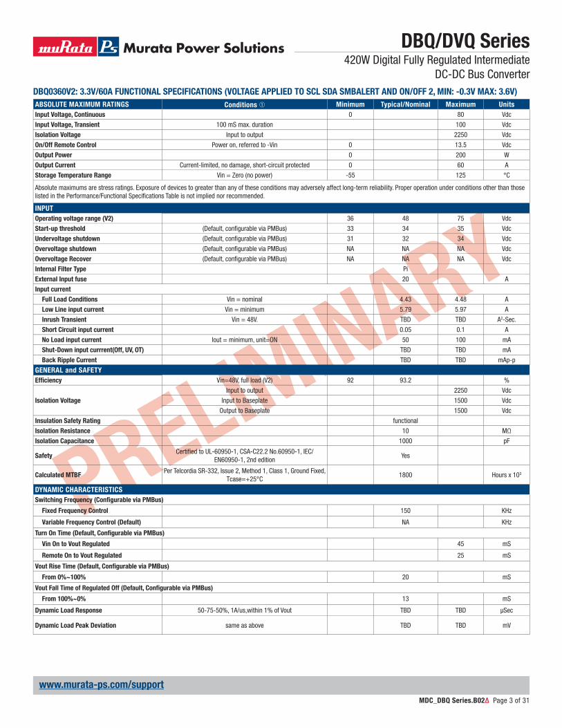
ABSOLUTE MAXIMUM RATINGS Conditions ➀ Minimum Typical/Nominal Maximum Units
Input Voltage, Continuous 0 80 Vdc
Input Voltage, Transient 100 mS max. duration 100 Vdc
Isolation Voltage Input to output 2250 Vdc
On/Off Remote Control Power on, referred to -Vin 0 13.5 Vdc
Output Power 0 200 W
Output Current Current-limited, no damage, short-circuit protected 0 60 A
Storage Temperature Range Vin = Zero (no power) -55 125 °C
Absolute maximums are stress ratings. Exposure of devices to greater than any of these conditions may adversely affect long-term reliability. Proper operation under conditions other than those listed in the Performance/Functional Specifi cations Table is not implied nor recommended.
INPUT
Operating voltage range (V2) 36 48 75 Vdc
Start-up threshold (Default, confi gurable via PMBus) 33 34 35 Vdc
Undervoltage shutdown (Default, confi gurable via PMBus) 31 32 34 Vdc
Overvoltage shutdown (Default, confi gurable via PMBus) NA NA NA Vdc
Overvoltage Recover (Default, confi gurable via PMBus) NA NA NA Vdc
Internal Filter Type Pi
External Input fuse 20 A
Input current
Full Load Conditions Vin = nominal 4.43 4.48 A
Low Line input current Vin = minimum 5.79 5.97 A
Inrush Transient Vin = 48V. TBD TBD A2-Sec.
Short Circuit input current 0.05 0.1 A
No Load input current Iout = minimum, unit=ON 50 100 mA
Shut-Down input currrent(Off, UV, OT) TBD TBD mA
Back Ripple Current TBD TBD mAp-p
GENERAL and SAFETY
Effi ciency Vin=48V, full load (V2) 92 93.2 %
Isolation Voltage
Input to output 2250 Vdc
Input to Baseplate 1500 Vdc
Output to Baseplate 1500 Vdc
Insulation Safety Rating functional
Isolation Resistance 10 MΩ
Isolation Capacitance 1000 pF
SafetyCertifi ed to UL-60950-1, CSA-C22.2 No.60950-1, IEC/
EN60950-1, 2nd edition Yes
Calculated MTBFPer Telcordia SR-332, Issue 2, Method 1, Class 1, Ground Fixed,
Tcase=+25°C 1800 Hours x 103
DYNAMIC CHARACTERISTICS
Switching Frequency (Confi gurable via PMBus)
Fixed Frequency Control 150 KHz
Variable Frequency Control (Default) NA KHz
Turn On Time (Default, Confi gurable via PMBus)
Vin On to Vout Regulated 45 mS
Remote On to Vout Regulated 25 mS
Vout Rise Time (Default, Confi gurable via PMBus)
From 0%~100% 20 mS
Vout Fall Time of Regulated Off (Default, Confi gurable via PMBus)
From 100%~0% 13 mS
Dynamic Load Response 50-75-50%, 1A/us,within 1% of Vout TBD TBD μSec
Dynamic Load Peak Deviation same as above TBD TBD mV
DBQ0360V2: 3.3V/60A FUNCTIONAL SPECIFICATIONS (VOLTAGE APPLIED TO SCL SDA SMBALERT AND ON/OFF 2, MIN: -0.3V MAX: 3.6V)
DBQ/DVQ Series420W Digital Fully Regulated Intermediate
DC-DC Bus Converter
MDC_DBQ Series.B02Δ Page 3 of 31

www.murata-ps.com/support
PRELIMINARY
FEATURES and OPTIONS Conditions ➀ Minimum Typical/Nominal Maximum Units
Remote On/Off Control
Primary On/Off control (designed to be driving with an open collector logic, Voltages referenced to -Vin)
“P” suffi x:
Positive Logic, ON state ON = pin open or external voltage 3.5 13.5 V
Positive Logic, OFF state OFF = ground pin or external voltage 0 0.8 V
Control Current open collector/drain 0.1 0.2 mA
“N” suffi x:
Negative Logic, ON state ON = ground pin or external voltage -0.1 0.8 V
Negative Logic, OFF state OFF = pin open or external voltage 3.5 13.5 V
Control Current open collector/drain 0.1 0.2 mA
OUTPUT
Total Output Power 0 198 200 W
Voltage
Setting Accuracy At 100% load, no trim, all conditions 3.27 3.3 3.33 Vdc
Output Adjust Range Confi gurable via PMBus 2.2 3.6 Vdc
Overvoltage Protection Confi gurable via PMBus 4 Vdc
Voltage Droop Default, confi gurable via PMBus 0 mΩ
Current
Output Current Range 0 60 60 A
Minimum Load No minimum load Current Limit Inception ➁ 98% of Vnom., after warmup, Confi gurable via PMBus 70 A
Short Circuit
Short Circuit Current Hiccup technique, autorecovery within 1% of Vout 0.4 1 A
Short Circuit Duration
(remove short for recovery)Output shorted to ground, no damage Continuous
Short circuit protection method, default
response, confi gurable via PMBusHiccup current limiting Non-latching
Regulation ➂
Line Regulation (V2) Vin = 36-75, Vout = nom., full load 20 mV
Load Regulation (V2) Iout = min. to max., Vin = nom. 15 mV
Ripple and Noise5 Hz- 20 MHz BW, Cout = 1μF 40 150 mV pk-pk
paralleled with 10μF
Temperature Coeffi cient At all outputs 0.01 0.02 % of Vnom./°C
Maximum Output Capacitance Low ESR 10,000 μF
Power Good—Negative logic (Confi gurable via PMBus)
Power good high stage voltage 2.4 3.6 Vdc
Power good low stage voltage 0 0.4 Vdc
Out voltage for power good off triggering Confi gurable via PMBus 2 2.3 2.5 Vdc
Out Voltage for power good on triggering Confi gurable via PMBus 2.6 2.8 3 Vdc
DBQ0360V2 FUNCTIONAL SPECIFICATIONS (CONT.)
DBQ/DVQ Series420W Digital Fully Regulated Intermediate
DC-DC Bus Converter
MDC_DBQ Series.B02Δ Page 4 of 31

www.murata-ps.com/support
PRELIMINARY
DBQ0360V2 FUNCTIONAL SPECIFICATIONS (CONT.)
PMBus Conditions ➀ Minimum Typical/Nominal Maximum Units
PMBus GENERAL
PMBus REV. 1.2. SMBALERT# is supported. PEC is supported. Linear data format used.
Bus speed 400 kHz
Logic high input 2 3.3 Vdc
Logic low input 0 0.8 Vdc
Logic high output 2.4 Vdc
Logic low output 0.4 Vdc
PMBus ADDRESSING
If the calculated PMBus address is 0d, 11d or 12d, SA0 or SA1 lefts open, default PMBus address 119d is assigned instead. PMBus address = 8x(SA0 value) + (SA1 value). SA0, SA1 value VS resistor connected to GND.
0 10 kΩ
1 22 kΩ
2 33 kΩ
3 47 kΩ
4 68 kΩ
5 100 kΩ
6 150 kΩ
7 220 kΩ
PMBus MONITORING ACCURACY
VIN_READ -2 2 %
VOUT_READ -1 1 %
IOUT_READ (> = 10A) -5 5 %
IOUT_READ (<10A) -1 1 A
TEMP_READ 5 5 °C
DIGITAL INTERFACE SPECIFICATIONS (PMBUS MONITORING & FUNCTIONAL DESCRIPTION)Fault Protection Specifi cations
Output Voltage, Over Voltage protection, OVP Factory default 4 V
VOUT_OV_FAULT_LIMIT, Confi gurable via
PMBus>VOUT_OV_WARM_LIMIT 3 4 V
Restart delay (default, Confi gurable via PMBus) 500 ms
Input Voltage, Input Over Voltage Protection Factory default NA V
Setpoint accuracy %
VIN_OV_FAULT_LIMIT (Confi gurable via
PMBus) ➃>VIN_OV_WARM_LIMIT NA V
Restart delay (default, Confi gurable via PMBus) ms
Input Voltage, Input Under Voltage Protection,
UVLOFactory default 32 V
Setpoint accuracy -2 2 %
VIN_UV_FAULT_LIMIT (Confi gurable via
PMBus) ➃<VIN_UV_WARM_LIMIT <VIN_OV_FAULT_LIMIT 32 75 V
Restart delay (default, Confi gurable via PMBus) 100 ms
Over Current Protection, OCP Setpoint accuracy (Io) -2.5 2.5 %
(factory default) 70 A
IOUT_OC_FAULT_LIMIT (Confi gurable via
PMBus) ➃>IOUT_OC_WARN_LIMT 0 75 A
Restart delay (default, Confi gurable via PMBus) 100 ms
Over Temperature Protection, OTP OT_FAULT_LIMIT (factory default) 120 °C
OT_FAULT_LIMIT (Confi gurable via PMBus) ➃ >OT_WARM_LIMIT 0 30 150 °C
OTP accuracy (factory default) 5 5 °C
Restart delay (default, Confi gurable via PMBus) 500 ms
DBQ/DVQ Series420W Digital Fully Regulated Intermediate
DC-DC Bus Converter
MDC_DBQ Series.B02Δ Page 5 of 31

www.murata-ps.com/support
PRELIMINARY
DBQ0360V2 FUNCTIONAL SPECIFICATIONS (CONT.)
MECHANICAL Conditions ➀ Minimum Typical/Nominal Maximum Units
Outline Dimensions (open frame) 2.3 x 1.45 x 0.48 Inches
(Please refer to outline drawing) L x W x H 58.4 x 36.83 x 12.19 mm
Outline Dimensions (with baseplate) 2.3 x 1.45 x 0.50 Inches
58.4 x 36.80 x 12.7 mm
Weight (open frame) TBD Ounces
Grams
Weight (with baseplate) TBD Ounces
Grams
Through Hole Pin Diameter 0.04 & 0.062 Inches
1.016 & 1.575 mm
Digital Interface Pin Diameter 0.02 0.5 Through Hole Pin Material Copper alloy TH Pin Plating Metal and Thickness Nickel subplate 98.4-299 μ-inches
Gold overplate 4.7-19.6 μ-inches
ENVIRONMENTAL
Operating Ambient Temperature Range with derating -40 85 °C
Operating Baseplate Temperature -40 110 °C
Storage Temperature Vin = Zero (no power) -55 125 °C
Thermal Protection/Shutdown (with “B” Suffi x,
default value, Confi gurable via PMBUS)Confi gurable Via PMBus 120 °C
Electromagnetic Interference External fi lter required; see B Class
Conducted, EN55022/CISPR22 emissions performance test.
RoHS rating RoHS-6
Notes➀ Typical at TA = +25°C under nominal line voltage and full-load conditions. All models are speci-
fi ed with external 1μF and 10μF capacitors in parallel across their output pins. All values are default, unless otherwise noted.
➁ Over-current protection is non-latching with auto recovery (hiccup).
➂ Regulation specifi cations describe the output voltage changes as the line voltage or load current is varied from its nominal or midpoint value to either extreme.
➃ See Operating information section.
DBQ/DVQ Series420W Digital Fully Regulated Intermediate
DC-DC Bus Converter
MDC_DBQ Series.B02Δ Page 6 of 31

www.murata-ps.com/support
PRELIMINARY
PERFORMANCE DATA
Effi ciency vs. Line Voltage and Load Current @ +25°C
70
80
75
85
90
95
100
5 10 15 20 25 30 35 40 45 50 6055
Load Current (A)
Effi
cie
ncy
(%
) VIN = 36VVIN = 48VVIN = 75V
DBQ/DVQ Series420W Digital Fully Regulated Intermediate
DC-DC Bus Converter
MDC_DBQ Series.B02Δ Page 7 of 31
Maximum Current Temperature Derating with baseplate(Vin = 48V, airfl ow from Vin- to Vin+)
Maximum Current Temperature Derating with baseplate(Vin = 48V, airfl ow from Vin to Vout)
0
10
20
30
40
50
60
70
30 40 50 60 70 80 85
0.5 m/s (100 LFM)1.0 m/s (200 LFM)1.5 m/s (300 LFM)2.0 m/s (400 LFM)2.5 m/s (500 LFM)3.0 m/s (600 LFM)
Ou
tpu
t C
urr
en
t (A
mp
s)
Ambient Temperature (°C)
0
10
20
30
40
50
60
70
30 40 50 60 70 80 85
0.5 m/s (100 LFM)1.0 m/s (200 LFM)1.5 m/s (300 LFM)2.0 m/s (400 LFM)2.5 m/s (500 LFM)3.0 m/s (600 LFM)
Ou
tpu
t C
urr
en
t (A
mp
s)
Ambient Temperature (°C)

www.murata-ps.com/support
PRELIMINARY
DBQ0260V2: 5V/60A FUNCTIONAL SPECIFICATIONS (VOLTAGE APPLIED TO SCL SDA SMBALERT AND ON/OFF 2, MIN: -0.3V MAX: 3.6V)
ABSOLUTE MAXIMUM RATINGS Conditions ➀ Minimum Typical/Nominal Maximum Units
Input Voltage, Continuous 0 80 Vdc
Input Voltage, Transient 100 mS max. duration 100 Vdc
Isolation Voltage Input to output 2250 Vdc
On/Off Remote Control Power on, referred to -Vin 0 13.5 Vdc
Output Power 0 303 W
Output Current Current-limited, no damage, short-circuit protected 0 60 A
Storage Temperature Range Vin = Zero (no power) -55 125 °C
Absolute maximums are stress ratings. Exposure of devices to greater than any of these conditions may adversely affect long-term reliability. Proper operation under conditions other than those listed in the Performance/Functional Specifi cations Table is not implied nor recommended.
INPUT
Operating voltage range (V2) 36 48 75 Vdc
Start-up threshold (Default, confi gurable via PMBus) 33 34 35 Vdc
Undervoltage shutdown (Default, confi gurable via PMBus) 31 32 34 Vdc
Overvoltage shutdown (Default, confi gurable via PMBus) NA NA NA Vdc
Overvoltage Recover (Default, confi gurable via PMBus) NA NA NA Vdc
Internal Filter Type Pi External Input fuse 20 A
Input current
Full Load Conditions Vin = nominal 6.59 6.72 A
Low Line input current Vin = minimum 8.77 8.86 A
Inrush Transient Vin = 48V. TBD TBD A2-Sec.
Short Circuit input current 0.05 0.1 A
No Load input current Iout = minimum, unit=ON 50 100 mA
Shut-Down input currrent(Off, UV, OT) TBD TBD mA
Back Ripple Current TBD TBD mAp-p
GENERAL and SAFETY
Effi ciency Vin=48V, full load (V2) 93 94.8 %
Isolation Voltage
Input to output 2250 Vdc
Input to Baseplate 1500 Vdc
Output to Baseplate 1500 Vdc
Insulation Safety Rating functional Isolation Resistance 10 MΩ
Isolation Capacitance 1000 pF
SafetyCertifi ed to UL-60950-1, CSA-C22.2 No.60950-1, IEC/
EN60950-1, 2nd edition Yes
Calculated MTBFPer Telcordia SR-332, Issue 2, Method 1, Class 1, Ground Fixed,
Tcase=+25°C 1800 Hours x 103
DYNAMIC CHARACTERISTICS
Switching Frequency (Confi gurable via PMBus)
Fixed Frequency Control 150 KHz
Variable Frequency Control (Default) NA KHz
Turn On Time (Default, Confi gurable via PMBus)
Vin On to Vout Regulated 45 mS
Remote On to Vout Regulated 25 mS
Vout Rise Time (Default, Confi gurable via PMBus)
From 0%~100% 20 mS
Vout Fall Time of Regulated Off (Default, Confi gurable via PMBus)
From 100%~0% 13 mS
Dynamic Load Response 50-75-50%, 1A/us,within 1% of Vout TBD TBD μSec
Dynamic Load Peak Deviation same as above TBD TBD mV
DBQ/DVQ Series420W Digital Fully Regulated Intermediate
DC-DC Bus Converter
MDC_DBQ Series.B02Δ Page 8 of 31

www.murata-ps.com/support
PRELIMINARY
DBQ0260V2 FUNCTIONAL SPECIFICATIONS (CONT.)
FEATURES and OPTIONS Conditions ➀ Minimum Typical/Nominal Maximum Units
Remote On/Off Control
Primary On/Off control (designed to be driving with an open collector logic, Voltages referenced to -Vin)
“P” suffi x:
Positive Logic, ON state ON = pin open or external voltage 3.5 13.5 V
Positive Logic, OFF state OFF = ground pin or external voltage 0 0.8 V
Control Current open collector/drain 0.1 0.2 mA
“N” suffi x:
Negative Logic, ON state ON = ground pin or external voltage -0.1 0.8 V
Negative Logic, OFF state OFF = pin open or external voltage 3.5 13.5 V
Control Current open collector/drain 0.1 0.2 mA
OUTPUT
Total Output Power 0 300 303 W
Voltage
Setting Accuracy At 100% load, no trim, all conditions 4.95 5 5.05 Vdc
Output Adjust Range Confi gurable via PMBus 3 5.5 Vdc
Overvoltage Protection Confi gurable via PMBus 6 Vdc
Voltage Droop Default, confi gurable via PMBus 0 mΩ
Current
Output Current Range 0 60 60 A
Minimum Load No minimum load Current Limit Inception ➁ 98% of Vnom., after warmup, Confi gurable via PMBus 70 A
Short Circuit
Short Circuit Current Hiccup technique, autorecovery within 1% of Vout 0.4 1 A
Short Circuit DurationOutput shorted to ground, no damage Continuous
(remove short for recovery)
Short circuit protection method, default
response, confi gurable via PMBusHiccup current limiting Non-latching
Regulation ➂
Line Regulation (V2) Vin = 36-75, Vout = nom., full load 30 mV
Load Regulation (V2) Iout = min. to max., Vin = nom. 25 mV
Ripple and Noise5 Hz- 20 MHz BW, Cout = 1μF 50 150 mV pk-pk
paralleled with 10μF
Temperature Coeffi cient At all outputs 0.01 0.02 % of Vnom./°C
Maximum Output Capacitance Low ESR 10,000 μF
Power Good—Negative logic (Confi gurable via PMBus)
Power good high stage voltage 2.4 3.6 Vdc
Power good low stage voltage 0 0.4 Vdc
Out voltage for power good off triggering Confi gurable via PMBus 3 3.5 4 Vdc
Out Voltage for power good on triggering Confi gurable via PMBus 3.75 4.25 4.75 Vdc
DBQ/DVQ Series420W Digital Fully Regulated Intermediate
DC-DC Bus Converter
MDC_DBQ Series.B02Δ Page 9 of 31

www.murata-ps.com/support
PRELIMINARY
DBQ0260V2 FUNCTIONAL SPECIFICATIONS (CONT.)
PMBus Conditions ➀ Minimum Typical/Nominal Maximum Units
PMBus GENERAL
PMBus REV. 1.2. SMBALERT# is supported. PEC is supported. Linear data format used.
Bus speed 400 kHz
Logic high input 2 3.3 Vdc
Logic low input 0 0.8 Vdc
Logic high output 2.4 Vdc
Logic low output 0.4 Vdc
PMBus ADDRESSING
If the calculated PMBus address is 0d, 11d or 12d, SA0 or SA1 lefts open, default PMBus address 119d is assigned instead. PMBus address = 8x(SA0 value) + (SA1 value). SA0, SA1 value VS resistor connected to GND.
0 10 kΩ
1 22 kΩ
2 33 kΩ
3 47 kΩ
4 68 kΩ
5 100 kΩ
6 150 kΩ
7 220 kΩ
PMBus MONITORING ACCURACY
VIN_READ -2 2 %
VOUT_READ -1 1 %
IOUT_READ (> = 10A) -5 5 %
IOUT_READ (<10A) -1 1 A
TEMP_READ 5 5 °C
DIGITAL INTERFACE SPECIFICATIONS (PMBUS MONITORING & FUNCTIONAL DESCRIPTION)Fault Protection Specifi cations
Output Voltage, Over Voltage protection, OVP Factory default 6 VVOUT_OV_FAULT_LIMIT, Confi gurable via
PMBus>VOUT_OV_WARM_LIMIT 3 6 V
Restart delay (default, Confi gurable via PMBus) 500 μS
Input Voltage, Input Over Voltage Protection Factory default NA V
Setpoint accuracy %
VIN_OV_FAULT_LIMIT (Confi gurable via
PMBus) ➃>VIN_OV_WARM_LIMIT NA V
Restart delay (default, Confi gurable via PMBus) μS
Input Voltage, Input Under Voltage Protection,
UVLOFactory default 32 V
Setpoint accuracy -2 2 %
VIN_UV_FAULT_LIMIT (Confi gurable via
PMBus) ➃<VIN_UV_WARM_LIMIT <VIN_OV_FAULT_LIMIT 32 75 V
Restart delay (default, Confi gurable via PMBus) 100 μS
Over Current Protection, OCP Setpoint accuracy (Io) -2.5 2.5 %
(factory default) 70 A
IOUT_OC_FAULT_LIMIT (Confi gurable via
PMBus) ➃>IOUT_OC_WARN_LIMT 0 75 A
Restart delay (default, Confi gurable via PMBus) 100 μS
Over Temperature Protection, OTP OT_FAULT_LIMIT (factory default) 120 °C
OT_FAULT_LIMIT (Confi gurable via PMBus) ➃ >OT_WARM_LIMIT 0 30 150 °C
OTP accuracy (factory default) 5 5 °C
Restart delay (default, Confi gurable via PMBus) 500 μS
DBQ/DVQ Series420W Digital Fully Regulated Intermediate
DC-DC Bus Converter
MDC_DBQ Series.B02Δ Page 10 of 31

www.murata-ps.com/support
PRELIMINARY
DBQ0260V2 FUNCTIONAL SPECIFICATIONS (CONT.)
Notes➀ Typical at TA = +25°C under nominal line voltage and full-load conditions. All models are speci-
fi ed with external 1μF and 10μF capacitors in parallel across their output pins. All values are default, unless otherwise noted.
➁ Over-current protection is non-latching with auto recovery (hiccup).
➂ Regulation specifi cations describe the output voltage changes as the line voltage or load current is varied from its nominal or midpoint value to either extreme.
➃ See Operating information section.
MECHANICAL Conditions ➀ Minimum Typical/Nominal Maximum Units
Outline Dimensions (open frame) 2.3 x 1.45 x 0.48 Inches
(Please refer to outline drawing) L x W x H 58.4 x 36.83 x 12.19 mm
Outline Dimensions (with baseplate) 2.3 x 1.45 x 0.50 Inches
58.4 x 36.80 x 12.7 mm
Weight (open frame) TBD Ounces
Grams
Weight (with baseplate) TBD Ounces
Grams
Through Hole Pin Diameter 0.04 & 0.062 Inches
1.016 & 1.575 mm
Digital Interface Pin Diameter 0.02
0.5
Through Hole Pin Material Copper alloy
TH Pin Plating Metal and Thickness Nickel subplate 98.4-299 μ-inches
Gold overplate 4.7-19.6 μ-inches
ENVIRONMENTAL
Operating Ambient Temperature Range with derating -40 85 °C
Operating Baseplate Temperature -40 110 °C
Storage Temperature Vin = Zero (no power) -55 125 °C
Thermal Protection/Shutdown (with “B” Suffi x,
default value, Confi gurable via PMBUS)Confi gurable Via PMBus 120 °C
Electromagnetic Interference External fi lter required; see B Class
Conducted, EN55022/CISPR22 emissions performance test.
RoHS rating RoHS-6
DBQ/DVQ Series420W Digital Fully Regulated Intermediate
DC-DC Bus Converter
MDC_DBQ Series.B02Δ Page 11 of 31

www.murata-ps.com/support
DBQ0135V2: 12V/35A FUNCTIONAL SPECIFICATIONS (VOLTAGE APPLIED TO SCL SDA SMBALERT AND ON/OFF 2, MIN: -0.3V MAX: 3.6V)
ABSOLUTE MAXIMUM RATINGS Conditions ➀ Minimum Typical/Nominal Maximum Units
Input Voltage, Continuous 0 80 Vdc
Input Voltage, Transient 100 mS max. duration 100 Vdc
Isolation Voltage Input to output 2250 Vdc
On/Off Remote Control Power on, referred to -Vin 0 13.5 Vdc
Output Power 0 428.4 W
Output Current Current-limited, no damage, short-circuit protected 0 35 A
SCL / SDA / SMBALERT / ON/OFF 2 -0.3 3.6 Vdc
Storage Temperature Range Vin = Zero (no power) -55 125 °CAbsolute maximums are stress ratings. Exposure of devices to greater than any of these conditions may adversely affect long-term reliability. Proper operation under conditions other than those listed in the Performance/Functional Specifi cations Table is not implied or recommended.INPUT
Operating voltage range (V2) 36 48 75 Vdc
Start-up threshold (Default, confi gurable via PMBus) 33 34 35 Vdc
Undervoltage shutdown (Default, confi gurable via PMBus) 31 32 34 Vdc
Internal Filter Type Pi
External Input fuse 20 A
Input current
Full Load Conditions Vin = nominal 9.19 9.44 A
Low Line input current Vin = minimum 12.25 12.59 A
Inrush Transient Vin = 48V. 1.3 2.6 A2-Sec.
Short Circuit input current 0.05 0.1 A
No Load input current Iout = minimum, unit=ON 75 112 mA
Shut-Down input currrent(Off, UV, OT) 20 30 mA
Back Ripple Current 20 40 mAp-p
GENERAL and SAFETY
Isolation Voltage
Input to output 2250 Vdc
Input to Baseplate 1500 Vdc
Output to Baseplate 1500 Vdc
Insulation Safety Rating functional
Isolation Resistance 10 MΩ
Isolation Capacitance 1500 pF
SafetyCertifi ed to UL-60950-1, CSA-C22.2 No.60950-1, IEC/
EN60950-1, 2nd edition Yes
Calculated MTBFPer Telcordia SR-332, Issue 2, Method 1, Class 1, Ground Fixed,
Tcase=+25°C1800 Hours x 103
DYNAMIC CHARACTERISTICS
Switching Frequency (Confi gurable via PMBus)
Fixed Frequency Control 175 KHz
Turn On Time (Default, Confi gurable via PMBus)
Vin On to Vout Regulated 60 mS
Remote On to Vout Regulated 25 mS
Vout Rise Time (Default, Confi gurable via PMBus)
From 0%~100% 20 mS
Vout Fall Time of Regulated Off (Default, Confi gurable via PMBus)
From 100%~0% 20 mS
Dynamic Load Response 50-75-50%, 0.1A/us,within 1% of Vout 200 300 μSec
Dynamic Load Peak Deviation same as above ±300 ±500 mV
DBQ/DVQ Series420W Digital Fully Regulated Intermediate
DC-DC Bus Converter
MDC_DBQ Series.B02Δ Page 12 of 31

www.murata-ps.com/support
DBQ0135V2 FUNCTIONAL SPECIFICATIONS (CONT.)
FEATURES and OPTIONS Conditions ➀ Minimum Typical/Nominal Maximum Units
Remote On/Off Control
Primary On/Off control (designed to be driving with an open collector logic, Voltages referenced to -Vin)
“P” suffi x:
Positive Logic, ON state ON = pin open or external voltage 3.5 13.5 V
Positive Logic, OFF state OFF = ground pin or external voltage 0 0.8 V
Control Current open collector/drain 0.1 0.2 mA
“N” suffi x:
Negative Logic, ON state ON = ground pin or external voltage -0.1 0.8 V
Negative Logic, OFF state OFF = pin open or external voltage 3.5 13.5 V
Control Current open collector/drain 0.1 0.2 mA
Secondary On/Off control (Pull up to 3.3V internally; ignored by default confi guration; see technical notes section) Voltages referenced to -Vout)
“P” suffi x:
Positive Logic, ON state ON = pin open or external voltage 1.5 3.3 V
Positive Logic, OFF state OFF = ground pin or external voltage 0 0.8 V
Control Current open collector/drain 0.03 0.06 mA
“N” suffi x:
Negative Logic, ON state ON = ground pin or external voltage 0 0.8 V
Negative Logic, OFF state OFF = pin open or external voltage 1.5 3.3 V
Control Current open collector/drain 0.03 0.06 mA
Remote Sense Compliance Sense pins connected externally to respective Vout pins
OUTPUT
Total Output Power 0 420 428.4 W
Voltage
Initial Output Voltage
(Default, Confi gurable via PMBus)@VIN = 48V Iout = 0A temp = 25C, both with/without "S" suffi x 11.990 12.030 Vdc
Output Voltage
(Default, Confi gurable via PMBus)@All condtions, without "S" suffi x, VOUT_DROOP = 0Ω 11.760 12.000 12.240 Vdc
Output Voltage
(Default, Confi gurable via PMBus)@All condtions , with"S" suffi x, VOUT_DROOP = 10mΩ
(12.000-Iout*0.01)*0.98
12.000-Iout*0.01(12.000-
Iout*0.01)*1.02Vdc
Over-Voltage Protection
(Default, Confi gurable via PMBus)
Direct feedbackFault response is confi gurable via PMBus
13.80 14.40 15.60 Vdc
Voltage Droop Default, Confi gurable via PMBus
Without "S" suffi x 0 mΩ
With "S" suffi x 10 mΩ
Current
Output Current Range 0 35 A
Minimum Load No minimum load
Current Limit Inception ➁ 90% of Vnom., after warmup, Confi gurable via PMBus 42 A
Short Circuit
Short Circuit Current Hiccup technique, autorecovery within 1% of Vout 0.4 1 AShort Circuit Duration
(remove short for recovery)Output shorted to ground, no damage Continuous
Short circuit protection method, default
response, confi gurable via PMBusHiccup current limiting Non-latching
Regulation ➂
Line Regulation (V2) Vin = 36-75, Vout = nom., full load 75 mV
Load Regulation (V2)
Vin=nom.Without S suffi x: Vout@min_load-Vout@max_load
With S suffi x: Vout@min_load-Vout@max_load-Iout*VOUT_DROOP45 mV
Ripple and Noise5 Hz- 20 MHz BW, Cout = 1μF
paralleled with 10μF100 150 mV pk-pk
Temperature Coeffi cient At all outputs 0.01 0.02 % of Vnom./°C
Maximum Output Capacitance Low ESR 10,000 μF
Power Good—Negative logic (Confi gurable via PMBus)
Power good high stage voltage 2.4 3.6 Vdc
Power good low stage voltage 0 0.4 Vdc
Out voltage for power good off triggering Confi gurable via PMBus 8.64 9.6 10.56 Vdc
Out Voltage for power good on triggering Confi gurable via PMBus 9.72 10.8 11.88 Vdc
DBQ/DVQ Series420W Digital Fully Regulated Intermediate
DC-DC Bus Converter
MDC_DBQ Series.B02Δ Page 13 of 31

www.murata-ps.com/support
DBQ0135V2 FUNCTIONAL SPECIFICATIONS (CONT.)
PMBus Conditions ➀ Minimum Typical/Nominal Maximum Units
PMBus GENERAL
PMBus REV. 1.2. SMBALERT# is supported. PEC is supported. Linear data format used.
Bus speed 400 kHz
Logic high input 2 3.3 Vdc
Logic low input 0 0.8 Vdc
Logic high output 2.4 3.6 Vdc
Logic low output -0.1 0.4 Vdc
PMBus ADDRESSING
If the calculated PMBus address is 0d, 11d or 12d, SA0 or SA1 lefts open, default PMBus address 119d is assigned instead. PMBus address = 8x(SA0 value) + (SA1 value). SA0,
SA1 value VS resistor connected to GND.
0 10 kΩ
1 22 kΩ
2 33 kΩ
3 47 kΩ
4 68 kΩ
5 100 kΩ
6 150 kΩ
7 220 kΩ
PMBus MONITORING ACCURACY
VIN_READ -2.5 2.5 %
VOUT_READ -1 1 %
IOUT_READ -1 1 A
TEMP_READ -5 5 °C
DIGITAL INTERFACE SPECIFICATIONS (PMBUS MONITORING & FUNCTIONAL DESCRIPTION)Fault Protection Specifi cations
Output Voltage, Over Voltage protection, OVP Factory default 14.4 V
VOUT_OV_FAULT_LIMIT, Confi gurable via PMBus >VOUT_OV_WARM_LIMIT 8.1 15.6 V
Restart delay (default, Confi gurable via PMBus) 500 mSVIN_OV_FAULT_LIMIT (Confi gurable via
PMBus) ➃>VIN_OV_WARM_LIMIT 34 110 V
Restart delay (default, Confi gurable via PMBus) 200 mSInput Voltage, Input Under Voltage Protec-
tion, UVLOFactory default 32 V
Setpoint accuracy -2 2 % VIN_UV_FAULT_LIMIT (Confi gurable via
PMBus) ➃<VIN_UV_WARM_LIMIT <VIN_OV_FAULT_LIMIT 32 75 V
Restart delay (default, Confi gurable via PMBus) 200 mS
Over Current Protection, OCP Setpoint accuracy (Io) -3 3 %
(factory default) 42 AIOUT_OC_FAULT_LIMIT (Confi gurable via
PMBus) ➃>IOUT_OC_WARN_LIMT 0 50 A
Restart delay (default, Confi gurable via PMBus) 500 mS
Over Temperature Protection, OTP OT_FAULT_LIMIT (factory default) 120 °C
OT_FAULT_LIMIT (Confi gurable via PMBus) ➃ >OT_WARM_LIMIT 0 30 150 °C
OTP accuracy (factory default) 5 5 °C
Restart delay (default, Confi gurable via PMBus) 500 mS
DBQ/DVQ Series420W Digital Fully Regulated Intermediate
DC-DC Bus Converter
MDC_DBQ Series.B02Δ Page 14 of 31

www.murata-ps.com/support
Notes➀ Typical at TA = +25°C under nominal line voltage and full-load conditions. All models are speci-
fi ed with external 1μF and 10μF capacitors in parallel across their output pins. All values are default, unless otherwise noted.
➁ Over-current protection is non-latching with auto recovery (hiccup).
➂ Regulation specifi cations describe the output voltage changes as the line voltage or load current is varied from its nominal or midpoint value to either extreme.
➃ See Operating information section.
MECHANICAL Conditions ➀ Minimum Typical/Nominal Maximum Units
Outline Dimensions (open frame) 2.3 x 1.45 x 0.48 Inches
(Please refer to outline drawing) L x W x H 58.4 x 36.83 x 12.19 mm
Outline Dimensions (with baseplate) 2.3 x 1.45 x 0.52 Inches
58.4 x 36.80 x 13.21 mm
Weight (open frame) 1.85 Ounces
52.5 Grams
Weight (with baseplate) 2.35 Ounces
66.8 Grams
Through Hole Pin Diameter 0.04 & 0.062 Inches
1.016 & 1.575 mm
Digital Interface Pin Diameter 0.020
0.5
Through Hole Pin Material Copper alloy
TH Pin Plating Metal and Thickness Nickel subplate 98.4-299 μ-inches
Gold overplate 4.7-19.6 μ-inches
ENVIRONMENTAL
Operating Ambient Temperature Range with derating -40 85 °C
Operating Baseplate Temperature -40 110 °C
Storage Temperature Vin = Zero (no power) -55 125 °CThermal Protection/Shutdown (with "B" Suffi x,
default value, Confi gurable via PMBus)Confi gurable Via PMBus 125 °C
Electromagnetic Interference
Conducted, EN55022/CISPR22
External fi lter required; see emissions performance test.
B Class
RoHS rating RoHS-6
DBQ0135V2 FUNCTIONAL SPECIFICATIONS (CONT.)
DBQ/DVQ Series420W Digital Fully Regulated Intermediate
DC-DC Bus Converter
MDC_DBQ Series.B02Δ Page 15 of 31

www.murata-ps.com/support
PERFORMANCE DATA
Effi ciency vs. Line Voltage and Load Current @ +25°C
Thermal image at 35A current with 48V input voltage, 30°C ambient temperature, and 100LFM air fl ow. Identifi able and recommended maximum value to be verifi ed in application.
70
80
75
85
90
95
100
0 100 200 300 400
Power Out (Watts)
Effi
cie
ncy
(%
)
VIN = 36VVIN = 48VVIN = 75V
DBQ/DVQ Series420W Digital Fully Regulated Intermediate
DC-DC Bus Converter
MDC_DBQ Series.B02Δ Page 16 of 31

www.murata-ps.com/support
PERFORMANCE DATA: TEMPERATURE DERATING
Open Frame With Baseplate
0
3
6
9
12
15
18
21
24
27
30
33
30 35 40 45 50 55 60 65 70 75 80 85
0.5 m/s (100 LFM)1.0 m/s (200 LFM)1.5 m/s (300 LFM)2.0 m/s (400 LFM)
Ou
tpu
t C
urr
en
t (A
mp
s)
Ambient Temperature (°C)
33
30
27
24
21
18
15
12
9
6
3
030 35 40 45 50 55 60 65 70 75 80 85
0.5 m/s (100 LFM)1.0 m/s (200 LFM)1.5 m/s (300 LFM)2.0 m/s (400 LFM)
Ou
tpu
t C
urr
en
t (A
mp
s)
Ambient Temperature (°C)
0
3
6
9
12
15
18
21
24
27
30
33
30 35 40 45 50 55 60 65 70 75 80 85
0.5 m/s (100 LFM)1.0 m/s (200 LFM)1.5 m/s (300 LFM)2.0 m/s (400 LFM)
Ou
tpu
t C
urr
en
t (A
mp
s)
Ambient Temperature (°C)
39
36
33
30
27
24
21
18
15
12
9
6
3
030 35 40 45 50 55 60 65 70 75 80 85
0.5 m/s (100 LFM)1.0 m/s (200 LFM)1.5 m/s (300 LFM)2.0 m/s (400 LFM)
Ou
tpu
t C
urr
en
t (A
mp
s)
Ambient Temperature (°C)
39
36
33
30
27
24
21
18
15
12
9
6
3
030 35 40 45 50 55 60 65 70 75 80 85
0.5 m/s (100 LFM)1.0 m/s (200 LFM)1.5 m/s (300 LFM)2.0 m/s (400 LFM)
Ou
tpu
t C
urr
en
t (A
mp
s)
Ambient Temperature (°C)
39
36
33
30
27
24
21
18
15
12
9
6
3
030 35 40 45 50 55 60 65 70 75 80 85
0.5 m/s (100 LFM)1.0 m/s (200 LFM)1.5 m/s (300 LFM)2.0 m/s (400 LFM)
Ou
tpu
t C
urr
en
t (A
mp
s)
Ambient Temperature (°C)
Maximum Current Temperature Derating at sea level(Vin = 36V, airfl ow from Vin to Vout)
Maximum Current Temperature Derating at sea level(Vin = 48V, airfl ow from Vin to Vout)
Maximum Current Temperature Derating at sea level(Vin = 75V, airfl ow from Vin to Vout)
Maximum Current Temperature Derating at sea level(Vin = 36V, airfl ow from Vin to Vout)
Maximum Current Temperature Derating at sea level(Vin = 48V, airfl ow from Vin to Vout)
Maximum Current Temperature Derating at sea level(Vin = 75V, airfl ow from Vin to Vout)
DBQ/DVQ Series420W Digital Fully Regulated Intermediate
DC-DC Bus Converter
MDC_DBQ Series.B02Δ Page 17 of 31

www.murata-ps.com/support
PERFORMANCE DATA
Startup Delay (Vin = 48V, Iout = 35A, Cout = 1000uF, Ta = +25°C)Ch1 = Vin, Ch2 = Vout
Output Ripple & Noise (Vin = 48V, Iout = 35A, Cout = 1uF || 10uF, Ta = +25°C)
Stepload Transient Response (Vin = 48V, Iout = 50-75-50% of Iout, Cload = 1uF || 10uF, slew rate: 0.1A/us, Ta = +25°C)
Enable Startup Delay (Vin = 48V, Iout = 35A, Cout = 1000uF, Ta = +25°C) Ch2 = Vout Ch4 = Enable
Output Ripple & Noise (Vin = 48V, Iout = 0A, Cout = 1uF || 10uF, Ta = +25°C)
DBQ/DVQ Series420W Digital Fully Regulated Intermediate
DC-DC Bus Converter
MDC_DBQ Series.B02Δ Page 18 of 31

www.murata-ps.com/support
MECHANICAL SPECIFICATIONS
Third Angle Projection
Dimensions are in inches (mm shown for ref. only).
Components are shown for reference onlyand may vary between units.
Tolerances (unless otherwise specified):.XX ± 0.02 (0.5).XXX ± 0.010 (0.25)Angles ± 2˚
INPUT/OUTPUT CONNECTIONS
Pin Designation Function
1 +VIN Positive Input
2 On/Off 1 Control Primary On/Off Control
3 No Pin No Pin
4 –VIN Negative Input
5 –VOUT Negative Output
6 +S Positive Remote Sense
7 –S Negative Remote Sense
8 SA0 Address Pin 0
9 SA1 Address Pin 1
10 SCL PMBus Clock
11 SDA PMBus Data
12 PG Power Good Output
13 DGND PMBus Ground
14 SMBALERT PMBus Alert Signal
15 On/Off 2 Control Secondary On/Off Control
16 +VOUT Positive Output
0.3
15
0.0
79
0.079
1013
1
2
586
16
SQ.0.02
highest component
SEE NOTE 6
between standoffs and 0.010 minimum clearance
0.4
8 M
ax
PIN SIDE VIEW
between standoffs and highest component
PINS 1,2,4:0.040±0.0015(1.016±0.038)
Shoulder: 0.076±0.005(1.93±0.13)PINS 5,16:0.062±0.0015(1.575±0.038)
Shoulder: 0.098±0.005(2.49±0.13)
0.010 minimum clearance
0.5
2 M
ax
M3 THREAD TYP 4PL
0.2
10
0.220
PINS 1,2,4,:0.040±0.0015(1.016±0.038)
Shoulder: 0.076±0.005(1.93±0.13)PINS 5,16:0.062±0.0015(1.575±0.038)
Shoulder: 0.098±0.005(2.49±0.13)
4
WITH BASEPLATE OPTION
97
111214
NOTES:
15
UNLESS OTHERWISE SPECIFIED;1:M3 SCREW USED TO BOLT UNIT'S BASEPLATE TO OTHER SURFACES(SUCH AS HEATSINK) MUST NOT EXCEED 0.100''(2.54mm) DEPTH BELOW THE SURFACE OF BASEPLATE2:APPLIED TORQUE PER SCREW SHOULD NOT EXCEED 5.3In-lb(0.6Nm);3:ALL DIMENSION ARE IN INCHES[MILIMETER];4:ALL TOLERANCES: ×.××in ,±0.02in(×.×mm,±0.5mm) ×.×××in ,±0.01in(×.××mm,±0.25mm)5:COMPONENT WILL VARY BETWEEN MODELS6:STANDARD PIN LENGTH: 0.180 Inch
PIN SIDE VIEW
OPEN FRAME
FOR L1 PIN LENGTH OPTION IN MODEL NAME, THE L LENGTH SHOULD BE 0.110 INCH FOR L2 PIN LENGTH OPTION IN MODEL NAME., USE STANDARD L2 PIN WITH PIN LENGTH TO 0.145 Inch
0.60
0 (1
5.24
)
2.30 (58.4)
2.30 (58.4)
2.000 (50.8)
2.000 (50.8)
0.60
0(1
5.24
)
1.0
30 (2
6.16
)
1.860 (47.24)
1.4
5 (3
6.83
)
1.4
5 (3
6.83
)
DBQ/DVQ Series420W Digital Fully Regulated Intermediate
DC-DC Bus Converter
MDC_DBQ Series.B02Δ Page 19 of 31

www.murata-ps.com/support
Each static dissipative polyethylene foam tray accommodates 15 converters in a 3 x 5 array.
9.92(251.97)
REF
9.92(251.97)
REF
0.88 (22.35)REF
Carton accommodates two (2) trays yielding 30 converters per carton
10.50 (266.7) ±.2511.00 (279.4) ±.25
2.75 (69.85) ±.25closed height
STANDARD PACKAGING
Third Angle Projection
Dimensions are in inches (mm) shown for ref. only.
Tolerances (unless otherwise specified):.XX ± 0.02 (0.5).XXX ± 0.010 (0.25)Angles ± 2˚
DBQ/DVQ Series420W Digital Fully Regulated Intermediate
DC-DC Bus Converter
MDC_DBQ Series.B02Δ Page 20 of 31

www.murata-ps.com/support
Power Management Overview
The module includes a wide range of readable and confi gurable power management features that are easy to implement with a minimum of external components. Furthermore, the module includes protection features that continuously protect the load from damage due to unexpected system faults. The SMBALERT pin alerts the host if there is a fault in the module. The follow-ing product parameters can continuously be monitored by a host: Vout, Iout, Vin, Temperature, and Power Good. The module is distributed with a default confi guration suitable for a wide range operation in terms of Vin, Vout, and load. All power management functions can be reconfi gured using the PMBus interface. The product provides a PMBus digital interface that enables the user to confi gure many aspects of the device operation as well as monitor the input and output parameters. Please contact our FAE for special confi gurations.
Soft-start Power Up
The default rise time of the ramp up is 20 ms. When starting by applying input voltage the control circuit boot-up time adds an additional 10 ms delay. The soft-start power up of the module can be reconfi gured using the PMBus interface.
Over Voltage Protection (OVP)
The module includes over voltage limiting circuitry for protection of the load. The default OVP limit is 20% above the nominal output voltage. If the output voltage surpasses the OVP limit, the module can respond in different ways. The default response from an over voltage fault is to immediately shut down. The device will continuously check for the presence of the fault condition, and when the fault condition no longer exists the device will be re-enabled. The OVP fault level and fault response can be reconfi gured using the PMBus interface.
Over Current Protection (OCP, Current limit)
The module includes current limiting circuitry for protection at continuous over load. The default setting for the product is hicup mode. The current limit could be confi gured by simply setting the IOUT_OC_FAULT_LIMIT to be greater than the IOUT_OC_WARN_LIMIT. The maximum value that the current limit could be set is 50A.
TECHNICAL NOTES
Power Good
The module provides Power Good (PG) fl ag in the Status Word register that indicates the output voltage is within a specifi ed tolerance of its target level and no fault condition exists. The Power Good pin default logic is negative and it can be confi gured by MFR_PGOOD_POLARITY.
PMBus Interface
This module offers a PMBus digital interface that enables the user to confi gure many characteristics of the device operation as well as to monitor the input and output voltages, output current and device temperature. The module can be used with any standard two-wire I2C or SMBus host device. In addition, the module is compatible with PMBus version 1.2 and includes an SMBALERT line to help alleviate bandwidth limitations related to continuous fault monitoring. The module supports 100 kHz and 400 kHz bus clock frequency only.
Monitoring via PMBus
A system controller (host device) can monitor a wide variety of parameters through the PMBus interface. The controller can monitor fault conditions by monitoring the SMBALERT pin, which will be asserted when any number of pre-confi gured fault or warning conditions occur. The system controller can also continuously monitor any number of power conversion parameters includ-ing but not limited to the following:
• Input voltage• Output voltage• Output current• Module temperature
Software Tools for Design and Production
For these modules, Murata-PS provides software for confi guring and monitor-ing via the PMBus interface. For more information please contact your local Murata-PS representative.
Click here for Application Note AN-63, Digital DC-DC Evaluation Board
User Guide.
Click here for Application Note AN-64, Murata Power Brick GUI User Manual.
DBQ/DVQ Series420W Digital Fully Regulated Intermediate
DC-DC Bus Converter
MDC_DBQ Series.B02Δ Page 21 of 31

www.murata-ps.com/support
PMBus Addressing
Figure 1 and the accompanying table display the recommended resistor values for hard-wiring PMBus addresses (1% tolerance resistors recommended): The address is set in the form of two octal (0 to 7) digits, with each pin setting one digit. The resistor values for each digit is shown below.
The SA0 and SA1 pins can be confi gured with a resistor to GND according to the following equation.
PMBus Address = 8 x (SA0value) + (SA1 value) C0 and C1 are 4.7nF capacitors, which are recommended for correct
addressing. If the calculated PMBus address is 0d, 11d or 12d, PMBus address 119d is assigned instead. From a system point of view, the user shall also be aware of further limitations of the addresses as stated in the PMBus Specifi ca-tion. It is not recommended to keep the SA0 and SA1 pins left open.
PMBus Commands
The products are designed to be PMBus compliant. The following tables list the implemented PMBus read commands. For more detailed information see “PMBus Power System Management Protocol Specifi cation, Part I – General Requirements, Transport and Electrical Interface” and “PMBus Power System Management Protocol, Part II – Command Language.”
Figure 1. Schematic of Connection of Address Resistors
SA0
SA1R1
C1
C0R0
Digit (SA0, SA1 index) Resistor Value [kΩ]
0 101 222 333 474 685 1006 1507 220
OVERALL
DBQ/DVQ Series420W Digital Fully Regulated Intermediate
DC-DC Bus Converter
MDC_DBQ Series.B02Δ Page 22 of 31
CMD Command Name1
SMBus
Transaction Type:
Writing Data
SMBus
Transaction Type:
Reading Data
Number
Of Data
Bytes
01h OPERATION2 Write Byte Read Byte 102h ON_OFF_CONFIG3 Write Byte Read Byte 103h CLEAR_FAULTS Send byte N/A 010h WRITE_PROTECT Write Byte Read Byte 111h STORE_DEFAULT_ALL4 Send byte N/A 012h RESTORE_DEFAULT_ALL4 Send byte N/A 015h STORE_USER_ALL4 Send byte N/A 016h RESTORE_USER_ALL4 Send byte N/A 019h CAPABILITY N/A Read Byte 120h VOUT_MODE N/A Read Byte 121h VOUT_COMMAND Write Word Read Word 222h VOUT_TRIM Write Word Read Word 225h VOUT_MARGIN_HIGH Write Word Read Word 226h VOUT_MARGIN_LOW Write Word Read Word 228h VOUT_DROOP Write Word16 Read Word 240h VOUT_OV_FAULT_LIMIT Write Word Read Word 241h VOUT_OV_FAULT_RESPONSE5 Write Byte Read Byte 142h VOUT_OV_WARN_LIMIT Write Word Read Word 246h IOUT_OC_FAULT_LIMIT Write Word Read Word 247h IOUT_OC_FAULT_RESPONSE6 Write Byte Read Byte 14Ah IOUT_OC_WARN_LIMIT Write Word Read Word 24Fh OT_FAULT_LIMIT Write Word Read Word 250h OT_FAULT_RESPONSE5 Write Byte Read Byte 151h OT_WARN_LIMIT Write Word Read Word 255h VIN_OV_FAULT_LIMIT Write Word Read Word 256h VIN_OV_FAULT_RESPONSE7 Write Byte Read Byte 157h VIN_OV_WARN_LIMIT Write Word Read Word 258h VIN_UV_WARN_LIMIT Write Word Read Word 259h VIN_UV_FAULT_LIMIT Write Word Read Word 25Ah VIN_UV_FAULT_RESPONSE7 Write Byte Read Byte 15Eh POWER_GOOD_ON Write Word Read Word 25Fh POWER_GOOD_OFF Write Word Read Word 2

www.murata-ps.com/support
DBQ/DVQ Series420W Digital Fully Regulated Intermediate
DC-DC Bus Converter
MDC_DBQ Series.B02Δ Page 23 of 31
CMD Command Name1
SMBus
Transaction Type:
Writing Data
SMBus
Transaction Type:
Reading Data
Number
Of Data
Bytes
60h TON_DELAY Write Word16 Read Word 261h TON_RISE14 Write Word16 Read Word 264h TOFF_DELAY Write Word16 Read Word 265h TOFF_FALL14 Write Word16 Read Word 278h STATUS_BYTE Write Byte Read Byte 179h STATUS_WORD Write Word Read Word 27Ah STATUS_VOUT Write Byte Read Byte 17Bh STATUS_IOUT Write Byte Read Byte 17Ch STATUS_INPUT Write Byte Read Byte 17Dh STATUS_TEMPERATURE Write Byte Read Byte 17Eh STATUS_CML Write Byte Read Byte 188h READ_VIN N/A Read Word 28Bh READ_VOUT N/A Read Word 28Ch READ_IOUT N/A Read Word 28Dh READ_TEMPERATURE_18 N/A Read Word 294h READ_DUTY_CYCLE N/A Read Word 295h READ_FREQUENCY N/A Read Word 296h READ_POUT N/A Read Word 298h PMBus_REVISION N/A Read Byte 199h MFR_ID N/A Block Read 229Ah MFR_MODEL9 N/A Block Read <=209Bh MFR_REVISION9 N/A Block Read <=109Dh MFR_DATE9 N/A Block Read <=109Eh MFR_SERIAL9 N/A Block Read <=10A0h MFR_VIN_MIN N/A Read Word 2A1h MFR_VIN_MAX N/A Read Word 2A2h MFR_IIN_MAX N/A Read Word 2A3h MFR_PIN_MAX N/A Read Word 2A4h MFR_VOUT_MIN N/A Read Word 2A5h MFR_VOUT_MAX N/A Read Word 2A6h MFR_IOUT_MAX N/A Read Word 2A7h MFR_POUT_MAX N/A Read Word 2A8h MFR_TAMBIENT_MAX N/A Read Word 2A9h MFR_TAMBIENT_MIN N/A Read Word 2B0h USER_DATA_00 Block Write Block Read <=20B1h USER_DATA_01 Block Write Block Read <=20C0h MFR_MAX_TEMP_1 N/A Read Word 2DBh MFR_CURRENT_SHARE_CONFIG N/A Read Byte 1DDh MFR_PRIMARY_ON_OFF_CONFIG Write Byte Read Byte 1DEh MFR_PGOOD_POLARITY Write Byte Read Byte 1E8h MFR_VIN_OV_FAULT_HYS Write Word Read Word 2E9h MFR_VIN_UV_FAULT_HYS Write Word Read Word 2EAh MFR_OT_FAULT_HYS Write Word Read Word 2
OVERALL (CONT.)

www.murata-ps.com/support
MURATA-PS DEFINED COMMANDS (01-CFH REFER TO PMBUS 1.2 SPEC)
DBh: MFR_CURRENT_SHARE_CONFIG
Bits Purpose Value Meaning
7:1 0000000 Reserved
0Droop Current Share Control
0 Current share disabled1 Droop current share mode enabled
DDh: MFR_PRIMARY_ON_OFF_CONFIG
Bits Purpose Value Meaning
7:3 00000 Reserved
2Controls how the unit responds to the CONTROL pin
0 Unit ignores the primary ON/OFF pin
1Unit requires the primary ON/OFF pin to be asserted to start the unit.
1Polarity of primary ON/OFF logic
0 Active low (Pull pin low to start the unit)1 Active high (Pull high or open to start the unit)
0 0 ReservedDEh: MFR_ PGOOD_POLARITY
Bits Purpose Value Meaning
7:1 0000000 Reserved
0Power good polarity of pin 12
0Negative logic, output low if Vout rises to specifi c value
1Positive logic, output high if Vout rises to specifi c value
Notes:1. a) Unit restores the entire contents of the non-volatile User Store memory when power up b) PEC is supported c) Max bus speed: 400kHZ d) SMBALERT# is supported e) Linear data format used f) addressing: If the calculated PMBus address is 0d, 11d or 12d, SA0 or SA1 lefts open, default
PMBus address 119d is assigned instead.2. Not supported items: 100101XXb Margin Low(Ignore Fault), 101001XXb On Margin High(Ignore Fault)3. Restart delay of turned off by OPEATION or CONTROL or primary on/off is 200ms4. Unit will shutdown 1 second for protection , then recover automatically.5. Restart delay unit: 500ms, lower limit: 500ms. Turn off delay unit: 0ms, lower limit: 0ms if bits 7:6=11b, restart delay is 500ms6. Restart delay unit and Turn off delay unit are same as note 5 Bits 7:6: 00b,01b,10b are not supported
7. Restart delay unit: 200ms, lower limit: 200ms. Turn off delay unit:0ms, lower limit: 0ms if bits 7:6=11b, restart delay is 200ms8. Temperature of baseplate side9. Unit's actual information10. Default value of DROOP CURRENT SHARE ENABLED mode: 0x01 Default value of DROOP CURRENT SHARE DISABLED mode: 0x0011. Locked to 10mΩ in DROOP CURRENT SHARE mode; confi gurable and default value is 0mΩ in
CURRENT SHARE DISABLED mode12. Default value of negative logic: 0x04 Default value of positive logic: 0x0613. Unit can receive any value for VOUT_TRIM command, but Vout is limited to 8.1~13.2V, if calcu-
lated Vout exceeds limit, then equal to limit.14. Value of 0 is acceptable, which is the same as lower limit to unit.15. Default value of without "B" suffi x: 120°C Default value of with "B" suffi x: 125°C 16. Confi gurable while without "S" suffi x locked while with "S" suffi x
On/Off 2 pin VOUT_DROOP TON_DELAY TOFF_DELAY TON_RISE TOFF_FALL
-- -- -- -- -- --On/Off 2 confi gurable confi gurable confi gurable confi gurable confi gurableOn/Off 2 locked to 0x000A locked to 0x0001 locked to 0x0000 locked to 0x0000 locked to 0x0000
DBQ/DVQ Series420W Digital Fully Regulated Intermediate
DC-DC Bus Converter
MDC_DBQ Series.B02Δ Page 24 of 31
OVERALL (CONT.)

www.murata-ps.com/support
STATUS WORD AND BYTE (GREEN = SUPPORTED)
STATUS_VOUT
7 VOUT_OV_FAULT6 VOUT_OV_WARNING5 VOUT_UV_WARNING4 VOUT_UV_FAULT3 VOUT_MAX Warning2 TON_MAX_FAULT1 TOFF_MAX_WARNING0 VOUT Tracking Error
STATUS_IOUT
7 IOUT_OC_FAULT6 IOUT_OC_LV_FAULT5 IOUT_OC_WARNING4 IOUT_UC_FAULT3 Current Share Fault2 In Power Limiting Mode1 POUT_OP_FAULT0 POUT_OP_WARNING
STATUS_TEMPERATURE
7 OT_FAULT6 OT_WARNING5 UT_WARNING4 UT_FAULT3 Reserved2 Reserved1 Reserved0 Reserved
STATUS_CML
7 Invalid/Unsupported Command6 Invalid/Unsupported Data5 Packet Error Check Failed4 Memory Fault Detected3 Processor Fault Detected2 Reserved1 Other Communication Fault0 Other Memory Or Logic Fault
STATUS_WORD
7 VOUT6 IOUT/POUT5 INPUT4 MFR_SPECIFIC3 POWER_GOOD#2 FANS1 OTHER0 UNKNOWN7 BUSY6 OFF5 VOUT_OV_FAULT4 IOUT_OC_FAULT3 VIN_UV_FAULT2 TEMPERATURE1 CML0 NONE OF THE ABOVE
STATUS_OTHER
7 Reserved6 Reserved5 Input A Fuse/Breaker Fault4 Input B Fuse/Breaker Fault3 Input A OR-ing Device Fault2 Input B OR-ing Device Fault1 Output OR-ing Device Fault0 Reserved
STATUS_INPUT
7 VIN_OV_FAULT6 VIN_OV_WARNING5 VIN_UV_WARNING4 VIN_UV_FAULT2 IIN_OC_FAULT1 IIN_OC_WARNING0 PIN_OP_WARNING
STATUS_MFR_SPECIFIC
Manufacturer Defi nedManufacturer Defi nedManufacturer Defi nedManufacturer Defi nedManufacturer Defi nedManufacturer Defi nedManufacturer Defi nedManufacturer Defi ned
STATUS_FANS_1_2
7 Fan 1 Fault6 Fan 2 Fault5 Fan 1 Warning4 Fan 2 Warning3 Fan 1 Speed Override2 Fan 2 Speed Override1 Air Flow Fault0 Air Flow Warning
STATUS_FANS_3_4
7 Fan 3 Fault6 Fan 4 Fault5 Fan 3 Warning4 Fan 4 Warning3 Fan 3 Speed Override2 Fan 4 Speed Override1 Reserved0 Reserved
DBQ/DVQ Series420W Digital Fully Regulated Intermediate
DC-DC Bus Converter
MDC_DBQ Series.B02Δ Page 25 of 31

www.murata-ps.com/support
TECHNICAL NOTES (CONT.)
DBQ/DVQ Series420W Digital Fully Regulated Intermediate
DC-DC Bus Converter
MDC_DBQ Series.B02Δ Page 26 of 31
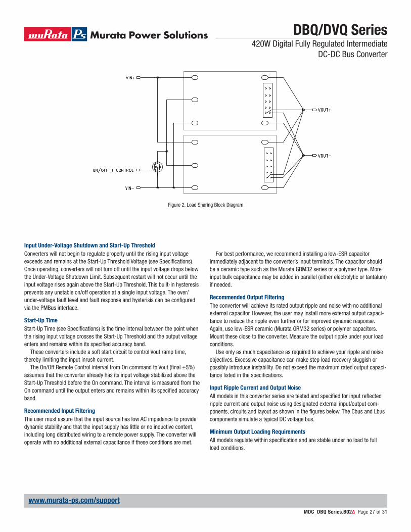
Parallel Load Sharing (S Option, Droop Load Sharing)
Two or more converters may be connected in parallel at both the input and output terminals to support higher output current (total power, see fi gure 2) or to improve reliability due to the reduced stress that results when the modules are operating below their rated limits. For applications requiring current share, followed the guidelines below. The products have a pre-confi gured voltage droop. The stated output voltage set point is at no load. The output voltage will decrease when the load current is increased. The voltage will drop 0.35V while load reaches max load. Our goal is to have each converter contribute nearly identical current into the output load under all input, environmental and load conditions.
Using Parallel Connections – Load Sharing (Power Boost)
Direct Connection Parallel Guidelines Use a common input power source. The input voltage must be between 36V and 75V.
+Vout and –Vout of all parallel units should be connected with a balance output impedance; +Sense and –Sense should be connected together (see fi gure 2).
Turn all units off before confi guring the output voltage via PMBus com-mands; all units must have the same output voltage confi guration.
It is recommended to turn on one unit fi rst and then turn other unit (s) on after the output for the fi rst one has settled. Turn on the next unit (s) after the previous unit reaches its regulated output voltage for at least 10mS. Users can use a different control signal to turn each unit on.
Users have the option to use a common primary or secondary Remote On/Off logic control signal to turn on modules at the same time after the input voltage rises above 36V.
If using PMBus to control units ON/OFF in parallel operation, we suggest to control one unit on fi rst. After the output voltage is stable, then make other units' output on.
First power up the parallel system (all converters) with a load not exceeding the rated load of 60%*35A*UNITS_QUANTITY and allow converters to settle (typically 20mS) before applying full load (90% load is recommended).
When converters are connected in parallel, allow for a safety factor of at least 10%. Up to 90% of max output current can be used from each module.
It is critical that the PCB layout incorporates identical connections from each module to the load; use the same trace rating and airfl ow/thermal environ-ments. If you add output fi lter components, use identical components and layout.
For Power-down, do not soft-off (GUI) while in parallel operation. Power down units by primary or secondary On/Off signal. Turn units off at the same time or one by one to avoid the OCP being triggered.
CAUTION: This converter is not internally fused. To avoid danger to persons or equipment and to retain safety certifi cation, the user must connect an external fast-blow input fuse as listed in the specifi cations. Be sure that the PC board pad area and etch size are adequate to provide enough current so that the fuse will blow with an overload.
Using Parallel Connections – Redundancy (N+1)
The redundancy connections require external user supplied “OR”ing diodes or “OR”ing MOSFETs for reliability purposes. The diodes allow for an uninterrupt-able power system operation in case of a catastrophic failure (shorted output) by one of the converters.
The diodes should be identical part numbers to enhance balance between the converters. The default factory nominal voltage should be suffi ciently matched between converters. The OR’ing diode system is the responsibility of the user. Be aware of the power levels applied to the diodes and possible heat sink requirements.
Schottky power diodes with approximately 0.3V drops or “OR”ing MOSFETs may be suitable in the loop whereas 0.7 V silicon power diodes may not be advisable. In the event of an internal device fault or failure of the mains power modules on the primary side, the other devices automatically take over the entire supply of the loads. In the basic N+1 power system, the “N” equals the number of modules required to fully power the system and “+1” equals one back-up module that will take over for a failed module. If the system consists of two power modules, each providing 50% of the total load power under normal operation and one module fails, another one delivers full power to the load. This means you can use smaller and less expensive power converters as the redundant elements, while achieving the goal of increased availability.
Thermal Shutdown
Extended operation at excessive temperature will initiate overtemperature shutdown triggered by a temperature sensor outside the PWM controller. This operates similarly to overcurrent and short circuit mode. The inception point of the overtemperature condition depends on the average power delivered, the ambient temperature and the extent of forced cooling airfl ow. Thermal shutdown uses only the hiccup mode (autorestart) and PMBus confi gurable hysteresis.
Start Up Considerations
When power is fi rst applied to the DC-DC converter, there is some risk of start up diffi culties if you do not have both low AC and DC impedance and adequate regulation of the input source. Make sure that your source supply does not allow the instantaneous input voltage to go below the minimum voltage at all times.
Use a moderate size capacitor very close to the input terminals. You may need two or more parallel capacitors. A larger electrolytic or ceramic cap sup-plies the surge current and a smaller parallel low-ESR ceramic cap gives low AC impedance.
Remember that the input current is carried both by the wiring and the ground plane return. Make sure the ground plane uses adequate thickness copper. Run additional bus wire if necessary.
Input Fusing
Certain applications and/or safety agencies may require fuses at the inputs of power conversion components. Fuses should also be used when there is the possibility of sustained input voltage reversal which is not current-limited. For greatest safety, we recommend a fast blow fuse installed in the ungrounded input supply line.
www.murata-ps.com/support
Input Under-Voltage Shutdown and Start-Up Threshold
Converters will not begin to regulate properly until the rising input voltage exceeds and remains at the Start-Up Threshold Voltage (see Specifi cations). Once operating, converters will not turn off until the input voltage drops below the Under-Voltage Shutdown Limit. Subsequent restart will not occur until the input voltage rises again above the Start-Up Threshold. This built-in hysteresis prevents any unstable on/off operation at a single input voltage. The over/under-voltage fault level and fault response and hysterisis can be confi gured via the PMBus interface.
Start-Up Time
Start-Up Time (see Specifi cations) is the time interval between the point when the rising input voltage crosses the Start-Up Threshold and the output voltage enters and remains within its specifi ed accuracy band.
These converters include a soft start circuit to control Vout ramp time, thereby limiting the input inrush current.
The On/Off Remote Control interval from On command to Vout (fi nal ±5%) assumes that the converter already has its input voltage stabilized above the Start-Up Threshold before the On command. The interval is measured from the On command until the output enters and remains within its specifi ed accuracy band.
Recommended Input Filtering
The user must assure that the input source has low AC impedance to provide dynamic stability and that the input supply has little or no inductive content, including long distributed wiring to a remote power supply. The converter will operate with no additional external capacitance if these conditions are met.
For best performance, we recommend installing a low-ESR capacitor immediately adjacent to the converter’s input terminals. The capacitor should be a ceramic type such as the Murata GRM32 series or a polymer type. More input bulk capacitance may be added in parallel (either electrolytic or tantalum) if needed.
Recommended Output Filtering
The converter will achieve its rated output ripple and noise with no additional external capacitor. However, the user may install more external output capaci-tance to reduce the ripple even further or for improved dynamic response. Again, use low-ESR ceramic (Murata GRM32 series) or polymer capacitors. Mount these close to the converter. Measure the output ripple under your load conditions.
Use only as much capacitance as required to achieve your ripple and noise objectives. Excessive capacitance can make step load recovery sluggish or possibly introduce instability. Do not exceed the maximum rated output capaci-tance listed in the specifi cations.
Input Ripple Current and Output Noise
All models in this converter series are tested and specifi ed for input refl ected ripple current and output noise using designated external input/output com-ponents, circuits and layout as shown in the fi gures below. The Cbus and Lbus components simulate a typical DC voltage bus.
Minimum Output Loading Requirements
All models regulate within specifi cation and are stable under no load to full load conditions.
DBQ/DVQ Series420W Digital Fully Regulated Intermediate
DC-DC Bus Converter
MDC_DBQ Series.B02Δ Page 27 of 31
Figure 2. Load Sharing Block Diagram

www.murata-ps.com/support
CINVIN CBUS
LBUS
CIN = 220μF, ESR < 700mΩ @ 100kHz
CBUS = 220μF, ESR < 100mΩ @ 100kHz
LBUS = 12μH
+Vin
-Vin
CURRENTPROBE
TO OSCILLOSCOPE
+–+–
Figure 3. Measuring Input Ripple Current
Thermal Shutdown (OTP, UTP)
To prevent many over temperature problems and damage, these converters include thermal shutdown circuitry. If environmental conditions cause the temperature of the DC-DCs to rise above the Operating Temperature Range up to the shutdown temperature, an on-board electronic temperature sensor will power down the unit. When the temperature decreases below the turn-on threshold set in the command recover temp is (OT_FAULT_LIMIT-MFR_OT_FAULT_HYS), the hysteresis is defi ned in general electrical specifi cation section. The OTP and hysteresis of the module can be reconfi gured using the PMBus. The OTP and UTP fault limit and fault response can be confi gured via the PMBus.
CAUTION: If you operate too close to the thermal limits, the converter may shut down suddenly without warning. Be sure to thoroughly test your applica-tion to avoid unplanned thermal shutdown.
Temperature Derating Curves
The graphs in this data sheet illustrate typical operation under a variety of conditions. The Derating curves show the maximum continuous ambient air temperature and decreasing maximum output current which is acceptable under increasing forced airfl ow measured in Linear Feet per Minute (“LFM”). Note that these are AVERAGE measurements. The converter will accept brief increases in current or reduced airfl ow as long as the average is not exceeded.
Note that the temperatures are of the ambient airfl ow, not the converter itself which is obviously running at higher temperature than the outside air. Also note that “natural convection” is defi ned as very fl ow rates which are not using fan-forced airfl ow. Depending on the application, “natural convection” is usually about 30-65 LFM but is not equal to still air (0 LFM).
Murata Power Solutions makes Characterization measurements in a closed cycle wind tunnel with calibrated airfl ow. We use both thermocouples and an infrared camera system to observe thermal performance. As a practical matter, it is quite diffi cult to insert an anemometer to precisely measure airfl ow in most applications. Sometimes it is possible to estimate the effective airfl ow if you thoroughly understand the enclosure geometry, entry/exit orifi ce areas and the fan fl owrate specifi cations.
CAUTION: If you exceed these Derating guidelines, the converter may have an unplanned Over Temperature shut down. Also, these graphs are all collected near Sea Level altitude. Be sure to reduce the derating for higher altitude.
Output Short Circuit Condition
The short circuit condition is an extension of the “Current Limiting” condition. When the monitored peak current signal reaches a certain range, the PWM controller’s outputs are shut off thereby turning the converter “off.” This is followed by an extended time out period. This period can vary depending on other conditions such as the input voltage level. Following this time out period, the PWM controller will attempt to re-start the converter by initiating a “normal start cycle” which includes softstart. If the “fault condition” persists, another “hiccup” cycle is initiated. This “cycle” can and will continue indefi nitely until such time as the “fault condition” is removed, at which time the converter will resume “normal operation.” Operating in the “hiccup” mode during a fault condition is advantageous in that average input and output power levels are held low preventing excessive internal increases in temperature.
Remote On/Off Control
The DBQ series modules are equipped with both primary (On/Off 1, enabled, pull up internal) and secondary (On/Off 2, disabled, pull up internal) control pins for increased system fl exibility. Both are confi gurable via PMBus. The On/Off pins are TTL open-collector and/or CMOS open-drain compatible. (See general specifi cations for threshold voltage levels. See also MFR_PRIMARY_ON_OFF_CONFIG section.)
Negative-logic models are on (enabled) when the On/Off is grounded or brought to within a low voltage (see specifi cations) with respect to –Vin. The device is off (disabled) when the On/Off is left open or is pulled high to +13.5Vdc with respect to –Vin. The On/Off function allows the module to be turned on/off by an external device switch.
Positive-logic models are enabled when the On/Off pin is left open or is pulled high to +13.5V with respect to –Vin. Positive-logic devices are disabled when the On/Off is grounded or brought to within a low voltage (see specifi ca-tions) with respect to –Vin. For voltage levels for On/Off 2 signal see functional specifi cations.
The restart delay for this module to turn On/Off by the On/Off control pin is 200ms.
C1 = 1μF; C2 = 10μF
LOAD 2-3 INCHES (51-76mm) FROM MODULE
RLOADC1 C2
SCOPE
+Vout
-Vout
Figure 4. Measuring Output Ripple and Noise (PARD)
On/Off 1 or 2 Control status
Not ignored Ignored
On/Off 1 or 2 pin P LOGIC N LOGIC P LOGIC N LOGICOPEN ON OFF ON ON
PULL HIGH ON OFF ON ONPULL LOW OFF ON ON ON
DBQ/DVQ Series420W Digital Fully Regulated Intermediate
DC-DC Bus Converter
MDC_DBQ Series.B02Δ Page 28 of 31
www.murata-ps.com/support
On/Off 1 can be confi gured by PMBus command MFR_PRIMARY_ON_OFF_CONFIG (DDh); default confi guration is not ignored; required On/Off 1 control pin to be asserted to start the unit.
On/Off 2 can be confi gured by PMBus command ON_OFF_CONFIG (02h); default confi guration is ignored; treat it as always ON.
DBQ's On/Off status is dependent on On/Off 1 control, On/Off 2 control, and OPERATION (PMBus command) status; all three must be ON to turn DBQ on; if one of them is OFF, unit will be turned off.
Output Capacitive Load
These converters do not require external capacitance added to achieve rated specifi cations. Users should only consider adding capacitance to reduce switching noise and/or to handle spike current load steps. Install only enough capacitance to achieve noise objectives. Excess external capacitance may cause degraded transient response and possible oscillation or instability.
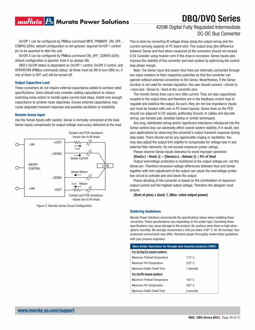
Remote Sense Input
Use the Sense inputs with caution. Sense is normally connected at the load. Sense inputs compensate for output voltage inaccuracy delivered at the load.
Figure 5. Remote Sense Circuit Confi guration
LOAD
Contact and PCB resistance losses due to IR drops
Contact and PCB resistance losses due to IR drops
+VOUT
+SENSE
−SENSE
-VOUT
−VIN
ON/OFFCONTROL
+VIN
Sense Current
I OUT
Sense Return
I OUT Return
Soldering Guidelines
Murata Power Solutions recommends the specifi cations below when installing these converters. These specifi cations vary depending on the solder type. Exceeding these specifi cations may cause damage to the product. Be cautious when there is high atmo-spheric humidity. We strongly recommend a mild pre-bake (100° C. for 30 minutes). Your production environment may differ; therefore please thoroughly review these guidelines
with your process engineers.
Wave Solder Operations for through-hole mounted products (THMT)
For Sn/Ag/Cu based solders:
Maximum Preheat Temperature 115° C.
Maximum Pot Temperature 270° C.
Maximum Solder Dwell Time 7 seconds
For Sn/Pb based solders:
Maximum Preheat Temperature 105° C.
Maximum Pot Temperature 250° C.
Maximum Solder Dwell Time 6 seconds
This is done by correcting IR voltage drops along the output wiring and the current carrying capacity of PC board etch. This output drop (the difference between Sense and Vout when measured at the converter) should not exceed 0.5V. Consider using heavier wire if this drop is excessive. Sense inputs also improve the stability of the converter and load system by optimizing the control loop phase margin.
Note: The Sense input and power Vout lines are internally connected through low value resistors to their respective polarities so that the converter can operate without external connection to the Sense. Nevertheless, if the Sense function is not used for remote regulation, the user should connect +Sense to +Vout and –Sense to –Vout at the converter pins.
The remote Sense lines carry very little current. They are also capacitively coupled to the output lines and therefore are in the feedback control loop to regulate and stabilize the output. As such, they are not low impedance inputs and must be treated with care in PC board layouts. Sense lines on the PCB should run adjacent to DC signals, preferably Ground. In cables and discrete wiring, use twisted pair, shielded tubing or similar techniques.
Any long, distributed wiring and/or signifi cant inductance introduced into the Sense control loop can adversely affect overall system stability. If in doubt, test your applications by observing the converter’s output transient response during step loads. There should not be any appreciable ringing or oscillation. You may also adjust the output trim slightly to compensate for voltage loss in any external fi lter elements. Do not exceed maximum power ratings.
Please observe Sense inputs tolerance to avoid improper operation:[Vout(+) −Vout(-)] − [Sense(+) −Sense(-)] ≤ 5% of Vout
Output overvoltage protection is monitored at the output voltage pin, not the Sense pin. Therefore excessive voltage differences between Vout and Sense together with trim adjustment of the output can cause the overvoltage protec-tion circuit to activate and shut down the output.
Power derating of the converter is based on the combination of maximum output current and the highest output voltage. Therefore the designer must ensure:
(Vout at pins) x (Iout) ≤ (Max. rated output power)
DBQ/DVQ Series420W Digital Fully Regulated Intermediate
DC-DC Bus Converter
MDC_DBQ Series.B02Δ Page 29 of 31

www.murata-ps.com/support
Emissions Performance
Murata Power Solutions measures its products for conducted emissions against the EN 55022 and CISPR 22 standards. Passive resistance loads are employed and the output is set to the maximum voltage. If you set up your own emissions testing, make sure the output load is rated at continuous power while doing the tests.
The recommended external input and output capacitors (if required) are included. Please refer to the fundamental switching frequency. All of this information is listed in the Product Specifi cations. An external discrete fi lter is installed and the circuit diagram is shown below.
[1] Conducted Emissions Parts List
[2] Conducted Emissions Test Equipment Used
Hewlett Packard HP8594L Spectrum Analyzer – S/N 3827A001532Line V-networks LS1-15V 50Ω/50Uh Line Impedance Stabilization Network
[3] Conducted Emissions Test Results
[4] Layout Recommendations
Most applications can use the fi ltering which is already installed inside the converter or with the addition of the recommended external capacitors. For greater emissions suppression, consider additional fi lter components and/or shielding. Emissions performance will depend on the user’s PC board layout, the chassis shielding environment and choice of external components. Please refer to Application Note GEAN-02 for further discussion.
Since many factors affect both the amplitude and spectra of emissions, we recommend using an engineer who is experienced at emissions suppression.
Reference Part Number Description Vendor
C1, C2, C3, C4, C5 GRM32ER72A105KA01LSMD CERAMIC-100V-
1000nF-X7R-1210Murata
C6 GRM319R72A104KA01DSMD CERAMIC100V-100nF-
±10%-X7R-1206Murata
L1, L2 PG0060TCOMMON MODE-473uH-
±25%-14A Pulse
C8, C9, C10, C11 GRM55DR72J224KW01LSMD CERAMIC630V-0.22uF-
±10%-X7R-2220Murata
C7 UHE2A221MHD Aluminum100V-220Uf-
±10%-long leadNichicon
C12 NA
LOADC2
L1
C6 C7DC/DC
C12
+ +
VCCRTN
-48V
GND
GND
C3C1L2
C5C4
C8 C9 C10 C11
Figure 6. Conducted Emissions Test Circuit
Graph 1. Conducted emissions performance, Positive Line, CISPR 22, Class B, full load
Graph 2. Conducted emissions performance, Negative Line, CISPR 22, Class B, full load
DBQ/DVQ Series420W Digital Fully Regulated Intermediate
DC-DC Bus Converter
MDC_DBQ Series.B02Δ Page 30 of 31

www.murata-ps.com/support
Murata Power Solutions, Inc. 11 Cabot Boulevard, Mansfi eld, MA 02048-1151 U.S.A.ISO 9001 and 14001 REGISTERED
This product is subject to the following operating requirements
and the Life and Safety Critical Application Sales Policy:
Refer to: http://www.murata-ps.com/requirements/Murata Power Solutions, Inc. makes no representation that the use of its products in the circuits described herein, or the use of other technical information contained herein, will not infringe upon existing or future patent rights. The descriptions contained herein do not imply the granting of licenses to make, use, or sell equipment constructed in accordance therewith. Specifi cations are subject to change without notice. © 2016 Murata Power Solutions, Inc.
DBQ/DVQ Series420W Digital Fully Regulated Intermediate
DC-DC Bus Converter
MDC_DBQ Series.B02Δ Page 31 of 31
Figure 7. Vertical Wind Tunnel
IR Video Camera
IR Transparentoptical window Variable
speed fan
Heating element
Ambient temperature
sensor
Airflowcollimator
Precisionlow-rate
anemometer3” below UUT
Unit undertest (UUT)
Vertical Wind Tunnel
Murata Power Solutions employs a computer controlled custom-designed closed loop vertical wind tunnel, infrared video camera system, and test instrumentation for accurate airfl ow and heat dissipation analysis of power products. The system includes a precision low fl ow-rate anemometer, variable speed fan, power supply input and load controls, temperature gauges, and adjustable heating element.
The IR camera monitors the thermal performance of the Unit Under Test (UUT) under static steady-state conditions. A special optical port is used which is transparent to infrared wavelengths.
Both through-hole and surface mount converters are soldered down to a 10" x 10" host carrier board for realistic heat absorption and spreading. Both longitudinal and trans-verse airfl ow studies are possible by rotation of this carrier board since there are often signifi cant differences in the heat dissipation in the two airfl ow directions. The combination of adjustable airfl ow, adjustable ambient heat, and adjustable Input/Output currents and voltages mean that a very wide range of measurement conditions can be studied.
The collimator reduces the amount of turbulence adjacent to the UUT by minimizing airfl ow turbulence. Such turbu-lence infl uences the effective heat transfer characteristics and gives false readings. Excess turbulence removes more heat from some surfaces and less heat from others, possibly causing uneven overheating.
Both sides of the UUT are studied since there are differ-ent thermal gradients on each side. The adjustable heating
element and fan, built-in temperature gauges, and no-contact IR camera mean that power supplies are tested in real-world
conditions.