Embed Size (px)
Citation preview

HiSIM2 1
シルバコ・ジャパン ワークショップ17.April, 2007
トランジスタの物理原理に基づく回路モデルHiSIMとその応用
広島大学先端物質科学研究科三浦道子

HiSIM2 2
0.はじめに
1.HiSIMの物理原理
2.CMOSのモデリング
3.SOI-MOSFETのモデリング
4.LDMOSのモデリング
5.イメージセンサのモデリング
6.MOS-Varactorのモデリング
7.研究開発とサポート環境について
目次

HiSIM2 3
HiSIM: Hiroshima-university STARC IGFET Model
1990 JJAP Sub-1μm MOSFETs short-channel effect model 1991 SISPAD “ 1st surface-potential-based model
parameter extraction strategy1994 ICCAD “ simulation time & stability verification1995 Siemens Flash-EEPROM concurrent device/circuit development1998 STARC 100-nm MOSFET collaboration start
Release Activity2001 Oct. release to vendors HiSIM1.0.0 source code and manual2002 Jan. release to public “ “
June “ HiSIM1.1.0 “Oct. “ HiSIM1.1.1 “
2003 Oct. Test release to STARC clients HiSIM2.0.0 source code and manual2005 May release to CMC members HiSIM2.0.0 “
July “ + Verilog-A codeOct. “ HiSIM2.2.0 “
2006 Jan. release to vendors HiSIM2.3.0 2006 Dec. “ HiSIM2.3.12007 March HiSIM2.4.0

HiSIM2 4
回路モデル
Compact Model: Meyer Model (1971)
Drain Current: Sah’s Equation
(drift近似)
2ds ox gs th ds ds
1( ) - 2
-μ ⎡ ⎤⎢ ⎥⎣ ⎦
WI = C V V V VL

HiSIM2 5
Vout
Vin
VDD
( ( ))( ) ( ( )) d Q V tI t I V td t
= +
過渡解析
Inverter:
conductivedisplacement
time
回路シミュレーターが解く式
モデルが回路シミュレーターに渡す情報
電流:Ι電荷:Q + 微分

HiSIM2 6
物理原理に基づく高精度高速計算
既存の回路モデル
Vth-Based Model (BSIM4)Surface-Potential-Based Model (HiSIM, PSP)Inversion-Charge-Based Model (ACM, EKV, BSIM5)
Nanotech’05

HiSIM2 7
基本デバイス方程式
SPICE )
s

HiSIM2 8
Vth-Based Model
Inversion-Charge-Based Model
linearization
2ds ox gs th ds ds
1( ) - 2
-μ ⎡ ⎤⎢ ⎥⎣ ⎦
WI = C V V V VL
drift近似

HiSIM2 9
Surface-Potential
(analytical)
(exact)
Vth-Based
Charge-Based
Models Year 9896 02 0400
BSIM(UC Barkeley)
Model11(Philips)
EKV(Swiss IT)
SP2000(Penn.SU)
HiSIM
CMC最終候補
決定
CMCによる標準化
PSP

HiSIM2 10
• Normalized run time based on HiSIM2.2.0/C: 2005年10月
– Through circuit-1-3, HiSIM/C runs faster than BSIM4.3.0. – In case of circuit-2, HiSIM/C is 30% faster than BSIM4.3.0.– In case of circuit-3, HiSIM/Verilog-A is 55% faster than PSP.– In case of circuit-4, Runtime comparison between HiSIM vs PSP is 1:25.
Circuit Source code Simulator BSIM4.3.0 HiSIM2.2.0 PSPC spice3f5 116 100 -
Verilog-A HSPICE 741 391 564C spice3f5 143 100 -
Verilog-A HSPICE no conv. 553 616C spice3f5 128 100 -
Verilog-A HSPICE 627 545 1227C spice3f5 no conv. 100 -
Verilog-A HSPICE no conv. no conv. 2549C spice3f5 no conv. 100 -
Verilog-A HSPICE 5136 no conv. 48005
4
3
2
1
STARChttp://www.eigroup.org/cmc/next_gen_cmos/phase3/phase3.html
計算時間の比較

HiSIM2 11HiSIM2.4.0はHiSIM2.3.1より約20%高速
Eval
uatio
n Ti
me
Vgs
HiSIM2.3.1BSIM4.5.0HiSIM2.4.0
評価法: default model-parameter values10000 nMOSFETs connected in parallelwith junction models, w/o leakage currents
L=W=1μmVds=1V, Vbs=0
計算スピードの比較

HiSIM2 12
0.はじめに
1.HiSIMの物理原理
2.CMOSのモデリング
3.SOI-MOSFETのモデリング
4.LDMOSのモデリング
5.イメージセンサのモデリング
6.MOS-Varactorのモデリング
7.研究開発とサポート環境について
目次

HiSIM2 13
HiSIMのモデリング法
HiSIM: 反復法
PSP: 解析式で近似
Poisson方程式を解く
計算スピード:
BSIM3<HiSIM231=BSIM4<PSP理由:
式の関数が単純モデルパラメタが少ない
長所:
様々のデバイスに容易に拡張可能

HiSIM2 14
表面ポテンシャルの比較
コンパクトモデルの精度の鍵

HiSIM2 15
Measurement
HiSIM
Wg/Lg=2μm/40nm
微分値の再現性

HiSIM2 16
45nmノードにおける電流の再現性
Measurement
HiSIM
Wg/Lg=2μm/200nm Wg/Lg=2μm/40nm

HiSIM2 17
Gummel Symmetry Test

HiSIM2 18
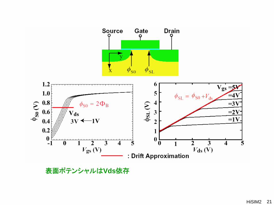
表面ポテンシャル
φSLは飽和する

HiSIM2 19
Pinch-off点以降の寄与
PSP: Vfb treated as channel length dependentHiSIM: inclusion of the lateral electric field
Inversion-Layer Thickness ~ 0Gradual-Channel Approximation Valid for long channel
近似:
短チャネル効果のモデル
ドレイン端でポテンシャルの急激な増加短チャネルで顕著

HiSIM2 20
(approximating a quadratic potential distribution)
短チャネル効果のモデル
M. Miura-Mattausch et al., IEEE TED, 48, p. 2449, 2001.
HiSIM2 21
表面ポテンシャルはVds依存

HiSIM2 22
ポケット注入モデル
高濃度注入によるポケットのテール
H. Ueno et al., IEEE T ED, 49, p. 1783, 2002.
V th
(V)

HiSIM2 23
: 2D-device simulation
Pocket Implantationwith NSUBP
ポケット濃度の予測性
デバイスばらつき予測に耐え得る

HiSIM2 24
極限動作で問題になる現象
高調波ひずみノイズNon-Quasi-Static効果デバイスばらつき

HiSIM2 25
Microscopicな特性
S. Laux et a., IBM J. Res. Develop., 34, p. 466, 1990.
Car
rier E
nerg
y
Position in the Channel
Macroscopicな特性
どこまで流体近似が有効か?
キャリア挙動
2ds ox gs th ds ds
1( ) - 2
-μ ⎡ ⎤⎢ ⎥⎣ ⎦
WI = C V V V VL

HiSIM2 26
Non-linearity
V(t)=Vgs+sin(2πf0t)
Higher-order derivatives of I-V characteristics are important.
高調波ひずみ
Good Surface-Potential Calculation

HiSIM2 27
Vds=0.1V
移動度との比較
Mobility determines the harmonic distortion characteristics.D. Navarro et al., Proc. SISPAD, p. 259, 2004.

HiSIM2 28
ノイズ特性
1/f NoiseThermal NoiseInduced Gate NoiseCross-Correlation Noise
Shot NoiseJunction Noise
d
dsi
Δ=
Noise Spectral Density
2i
Sf

HiSIM2 29
Different Origins
1/f Noise:
Thermal Noise:
Induced Gate Noise:Cross-Correlation Noise:

HiSIM2 30
1/f ノイズの起源

HiSIM2 31
1/fからのずれ

HiSIM2 32
Trap Densityの不均一性

HiSIM2 33
Wafer上の統計
Homogeneous Distribution on a Wafer

HiSIM2 34
モデル式

HiSIM2 35
Ntrap is fitted to measurements.If technology is mature, Ntrap is nearly universal.
測定値との比較
I-V characteristics determine 1/f noise characteristics.1/f noise is predictable.
S. Matsumoto et al., IEIEC T E, E88-C, p. 247, 2005.

HiSIM2 36
22 ds
eff ds
ds0
id4 ( )
4
kTS g yL IkTg γ
=
=
∫ dy gds0: at Vds=0
van der Ziel Equation based on Nyquist Theorem:
gds(y): Channel Conductance
γ : Noise Coefficient
Thermal Noiseの起源

HiSIM2 37
測定値との比較
Lg=0.17μmLg=0.3μmLg=0.5μmLg=1.0μm
Lines: HiSIMSymbols: Measurements
No Additional Model Parameters

HiSIM2 38
• Knoblinger et al. (2001): Hot Electron Contribution• Jamal Deen et al. (2002): Channel Length Modulation• Scholten et al. (2002): Velocity Saturation
短チャネルにおけるノイズ係数, γ
Different Explanations

HiSIM2 39
First γ Reduction and Increase in the Saturation RegionNo Drastic Increase of γ γ Minimum Increase from 2/3
Lines: Simulation (HiSIM) Symbols: Measurements
Potential Increase Mobility ReductionOrigin of γ IncreaseS. Hosokawa et al., Appl. Phys. Lett., vol. 87, p. 092104, 2005.
測定値との比較:Excess Noise

HiSIM2 40
Universal Relationship
Vth Shiftとの比較
Grad. γ
Grad. ΔVth

HiSIM2 41
T. Warabino et al., Proc. SISPAD, p. 158, 2006.
Induced Gate Noise と Cross-Correlation Noise

HiSIM2 42
g ch th0
0
0
( ) ( )
( ) ( ) ( )
( ) ( )
V x V V x V
V x V x v x
I x I I x
= − −
= − Δ⎧⎪⎨ = − Δ⎪⎩
{ }( )( )
( ) ( ) ( )
i x Wj v x
x d
dV x V x I x
x W
εω
εμ
⎧⎪
∂⎪ = −⎪⎪ ∂⎨⎪⎪ ∂⎪ = −
∂⎪⎩
Continuity eq.
Current Density eq.
( )( ) ( )
g
g d
i
i i
g
g d
22
1 2
1 2 2
2
2**
i I I
i i I I I
S dx v dx
S dx v dx
′ ′Δ Δ + Δ
′ ′ ′Δ Δ Δ + Δ Δ
∴ = = Δ
= = Δ
∫ ∫
∫ ∫
: cross - correlation
M. Shoji, IEEE TED, pp. 520-524, 1966.
HiSIM2 43
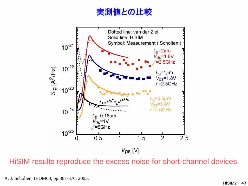
実測値との比較
HiSIM results reproduce the excess noise for short-channel devices.
A. J. Scholten, IEDM03, pp.867-870, 2003.

HiSIM2 44
ノイズ相関計数 c
HiSIM results reproduce the theoretical features of the cross-correlation.
i i
i i
g d
g d
Sc
S S=Correlation Coefficient :

HiSIM2 45
Excess Noiseの比較
Excess noise in Sig starts to saturate for further Vds increase.
Reason: mobility distribution along the channel
iggs
ds0
2
54C
gS kTω
β⎛ ⎞⎜ ⎟⎝ ⎠=

HiSIM2 46
Quasi-Static Approximation: spontaneous carrier response
Non-Quasi-Static Effects
( ( ))( ) ( ( )) d Q V tI t I V td t
= +

HiSIM2 47
キャリアの遅延
Carrier Deficit in the Channel

HiSIM2 48
NQS効果のモデリング
N. Nakayama et al., IEE Electron. Lett., 40, p. 276, 04.
Channel Segmentation

HiSIM2 49
Performance of an Element: PLL
0
0.5
1
1.5
2
0 0.2 0.4 0.6 0.8 1.0
Voltage [V]
TIME[nsec]
Fourier Transform
0
5000
1 104
1.5 104
2 104
2.5 104
3.0 6.0 9.0Spectrum[V2/Hz]
Frequency[GHz]
Time-Domain Analysis Frequency-Domain Analysis

HiSIM2 50
Numerical AC Analysis
Analytical Transformation
Numerical AC Analysis
Analytical Transform
K. Machida et al., SiRF, P. 57, 2006.
Analytical Transformation
Consistent Model both for Time- and Frequency-Domain Analysis

HiSIM2 51
S. Jinbou et al., Ext. Abs. SSDM, P. 26, 2002.
with Rg without Rg
Y-Parameter Analysis
Strong External Contribution

HiSIM2 52
Conventionalな方法
H. Kawano et al., Digest Microwave Symp., P. 2121, 2002.
Equivalent-Circuit Modelwith Substrate Network
パラメタ抽出が困難NQSモデルが本質

HiSIM2 53
高周波における高調波ひずみ
Carrier transit delay dominates the HD characteristics.
D. Navarro et al., IEEE T ED, vol. 53, p. 2025, 2006.

HiSIM2 54
Y. Takeda et al., CICC, p. 827, 2005.D. Navarro et al., IEEE MWC Lett., p. 125, 2006.
f0 = 1kHz
IP3 Prediction

HiSIM2 55
1/f Noise Thermal Noise
No model parameters are required.Features are determined only by I-V characteristics.
Harmonic Distortion
高次特性
Electrostatic effect is still dominating.
Surface potential is important.

HiSIM2 56
[Phenomena] [Subjects]
Short Channel:
Reverse-short Channel: impurity pile-uppocket implant
Poly-Depletion:
Quantum-Mechanical:
Channel-Length Modulation:
Narrow-Channel:
Temperature Dependency: thermal voltagebandgapniphonon scatteringmaximum velocity
Mobility Models: universalhigh Field
Shallow-Trench Isolation: threshold voltagemobilityleakage current
Capacitances: intrinsicoverlaplateral-field inducedfringing
[Phenomena] [Subjects]
Non-Quasi-Static: transient time-domainAC frequency-domein
Noise: 1/f thermal induced gatecross-correlation
Leakage Currents: substrate currentgate currentGIDL current
Source/Drain Resistances:
Junction Diode: currentscapacitances
HiSIM2でモデル化されている現象

HiSIM2 57
Binning OptionUser Required Improvements
DFM SupportBrushed up Source Code
HiSIM2.4.0: release March’07
e. g. STI-Model Improvements
HiSIM2.3.0 HiSIM2.3.1Parameter Extraction Procedure / Tools
Tests with Real Production Circuits
about 1 year
ばらつき予測

HiSIM2 58
0.はじめに
1.HiSIMの物理原理
2.CMOSのモデリング
3.SOI-MOSFETのモデリング
4.LDMOSのモデリング
5.イメージセンサのモデリング
6.MOS-Varactorのモデリング
7.研究開発とサポート環境について
目次

HiSIM2 59
MOSFET SOI-MOSFET DG-MOSFET Fin-FET
production
Motivation for Technology Innovation
高密度化
高性能化
高生産性
Siliconの微細化技術の開発

HiSIM2 60
2D-Device
表面ポテンシャルの計算

HiSIM2 61
HiSIM-SOI
現在History効果の検証:dynamic fully-, partially-depletion change

HiSIM2 62
1/fノイズ特性

HiSIM2 63
Bulk-MOSFETとの比較
HiSIM2 64
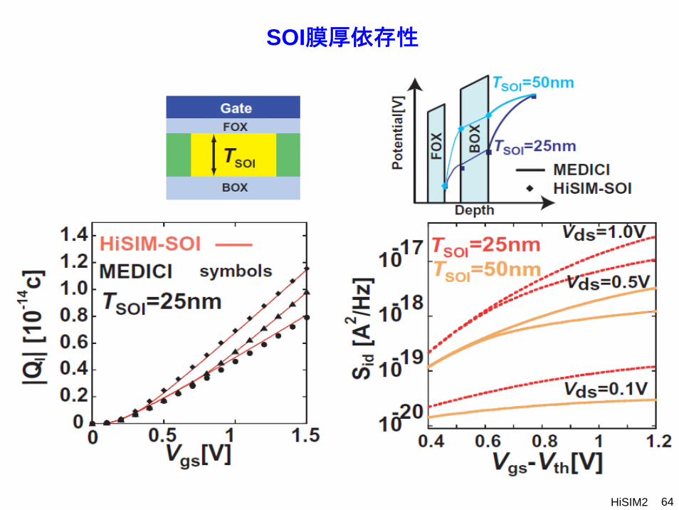
SOI膜厚依存性

HiSIM2 65
0.はじめに
1.HiSIMの物理原理
2.CMOSのモデリング
3.SOI-MOSFETのモデリング
4.LDMOSのモデリング
5.イメージセンサのモデリング
6.MOS-Varactorのモデリング
7.研究開発とサポート環境について
目次

HiSIM2 66
Different LDMOS StructuresCase 1.
Case 2.
Case 3.
Ldrift
Lover
Ldrift
Lover
Ldrift
Small overlap
LDMOS構造
Large overlap
Medium overlap

HiSIM2 67
Channel-Length ModulationOverlap Capacitance
HiSIM for Bulk-MOSFET
Complete Surface-Potential-Based Model
Beyond Gradual-Channel Approximation
φS0 : at source edge
φSL : at the end of the gradual-channel approx.
φS(ΔL) : at drain edge (calculated from φSL)

HiSIM2 68
Ldrift
Ndrift
1. Drift Regionのモデル化
Potential drop in the drift region
All important potential values are known.No sub-circuit for the potential drop is necessary.

HiSIM2 69
Comparison of Key Potential Values
: potential determining LDMOS characteristics
HiSIM reproduces φS(ΔL) calculated by 2D-device simulator.
φS(ΔL)φ S
(ΔL)
[V]
φS(ΔL)
φ S(Δ
L)[V
]
φ S(Δ
L)[V
]φ S
(ΔL)
[V]
Vgs [V] Vds [V]

HiSIM2 70
Comparison of Id-Vgs
: 2D-Device Simulation Results: HiSIM-LDMOS Results
I d[A
]
Vds=20V
Vds=10V
Vds=5V
Vds=0.1V
Good agreement between HiSIM result and 2D-device simulation result is achieved.
g m[S
]

HiSIM2 71
Comparison of Id-Vds
: 2D-Device Simulation Results: HiSIM-LDMOS Results
I d[A
]
Vgs=2.5V
Vgs=5V
Vgs=7.5V
Vgs=10V
Quasi-saturation behavior of LDMOS is reproduced.
g d[S
]

HiSIM2 72
Ldrift = 1.5μm Vds = 10V
invgs
QV
∂∂
driftC
invdrift
gs
Q CV
∂+
∂
Charge in the drift region is modeled explicitly.
Vgs [V] Vgs [V]
Comparison of Key Capacitances

HiSIM2 73
Lover
Ldrift
2.Gate-Drain Overlap領域のモデル化
Overlap領域でのdepletion, accumulation状態を考慮
Effect of GateEffect of Gate--Drain OverlapDrain Overlap

HiSIM2 74
0.はじめに
1.HiSIMの物理原理
2.CMOSのモデリング
3.SOI-MOSFETのモデリング
4.LDMOSのモデリング
5.イメージセンサのモデリング
6.MOS-Varactorのモデリング
7.研究開発とサポート環境について
目次

HiSIM2 75
Commercial use:- Sensor arrays with integrated processingcircuitry (for e. g. digital cameras)
Under R & D:- Opto-electronic integatedcircuits (OEICs)
- Prosthetic health care(e. g. artificial eye)
OEIC concept
HiSIM-PD

HiSIM2 76
Modeling of Lateral Photodiode
Approximations:
- Homogeneous field E inhorizontal (x) direction
- Holes move to p+ regioninstantly
- Negligible recombinationin intrinsic region

HiSIM2 77
Negligible Recombination
Main Justification:
- Low carrierconcentration in i-region
- Fast separation of generated carrierpairs
xy
n x y t J x y t G y tt q x
J x y t q n x y t E y
G y t e t
( , , ) 1 ( , , ) ( , )
( , , ) ( , , ) (: )
( , ) ( ): α
μ
α φ−
∂ ∂− =
∂ ∂=
=
電流連続の式:
電流密度式
キャリア発生確率
μ φα
⎛ ⎞⎜ ⎟⎝ ⎠
: elementary charge, : mobility, : photon flux,: absorption coefficient, : carrier number density, : current density
qn J
HiSIM2 78
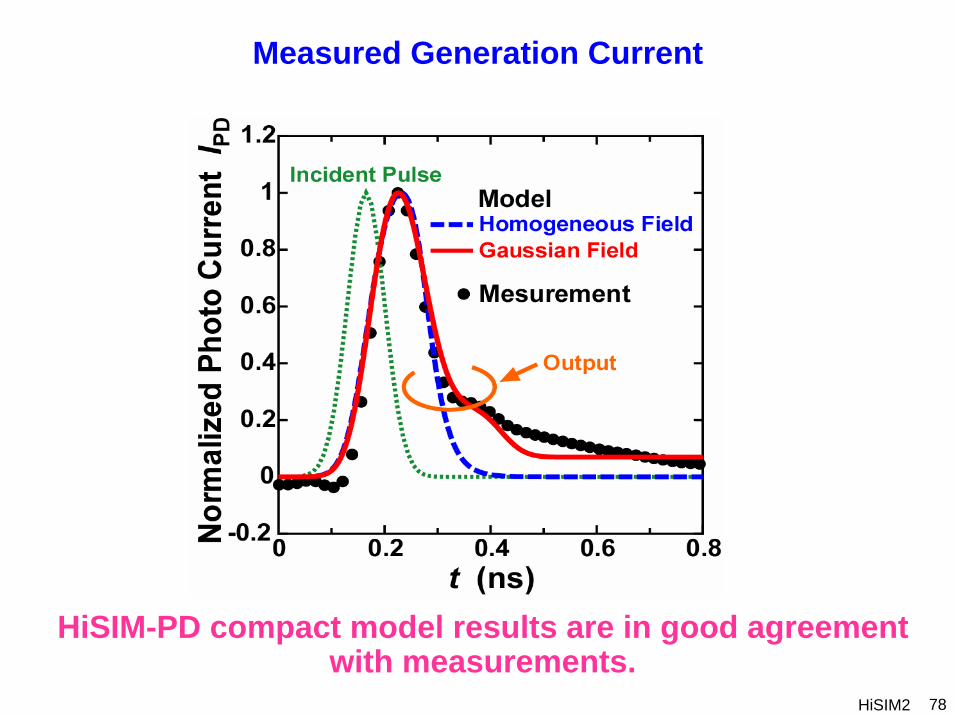
Measured Generation Current
HiSIM-PD compact model results are in good agreement with measurements.

HiSIM2 79
Attenuation-Length Dependence
A small attenuation length results in an extended current tail.

HiSIM2 80
Integration into Circuit Simulator
HiSIM-PD receives terminal voltages and to responds with the respective photocurrents.

HiSIM2 81
Consistent Simulation Necessity
Is a phenomenological current source model already a satisfactory solution ?

HiSIM2 82
Simulated Test Configuration
Tested dependencies:
- Vout (RL)- IPD (RL)
Compared methods:- HiSIM-PD model- Current source model- 2-D device simulation

HiSIM2 83
Comparison with Current Source
HiSIM-PD and current source results are even qualitatively different.

HiSIM2 84
Comparison with Device Simulator
2-D device simulation verifies the correctness of the HiSIM-PD results.

HiSIM2 85
0.はじめに
1.HiSIMの物理原理
2.CMOSのモデリング
3.SOI-MOSFETのモデリング
4.LDMOSのモデリング
5.イメージセンサのモデリング
6.MOS-Varactorのモデリング
7.研究開発とサポート環境について
目次

HiSIM2 86
AccumulationモードMOS Varactor

HiSIM2 87
キャリアの移動遅延: τ
τは電場に反比例する

HiSIM2 88
ΜΟS Varactorの周波数依存性

HiSIM2 89
0.はじめに
1.HiSIMの物理原理
2.CMOSのモデリング
3.SOI-MOSFETのモデリング
4.LDMOSのモデリング
5.イメージセンサのモデリング
6.MOS-Varactorのモデリング
7.研究開発とサポート環境について
目次

HiSIM2 90
ナノデバイス・システム研究センター
HiSIM研究センター
極微細デバイス工学STARC
准教授特認助手客員教授研究員
HiSIM研究センターの役割
A 会社
B 会社広島大学
教授准教授
教授准教授


![オブジェクト指向モデリング [6]](https://img.pdfslide.net/doc/110x75/56813a73550346895da26d15/-656813a73550346895da26d15.jpg)