Embed Size (px)
Citation preview
STUDY ON IN0.53GA0.47As MOS DEVICES WITH
PLASMA-PH3/N2 TREATMENT AND DEVICE
STRUCTURE OPTIMIZATION
SUMARLINA AZZAH BTE SULEIMAN
(B. Eng.(Hons.), NUS)
A Thesis Submitted for the Degree of Doctor of
Philosophy
Department of Electrical and Computer Engineering
National University of Singapore
2013

i

ii
Acknowledgements
I would like to acknowledge my supervisors, Prof. Lee Sungjoo and
Prof. Ganesh Samudra for their knowledge, insightful guidance,
encouragement and sincere concern throughout my graduate course, as well
as giving me the opportunity to research this interesting field. They had
always been there to listen and to give advice, and showed different possible
ways to approach a research problem. Their dedication to research has
touched my heart and motivated me to be persistent to accomplish any goal.
I am also very grateful to Chartered Semiconductor Manufacturing,
Ltd. (now known as GLOBALFOUNDRIES) for the financial support and
to Dr. Chan Lap, Dr. Ng Chee Mang as well as Dr Leong Kam Chew, not
only for their teaching and training but also for their valuable advice on my
future career. In addition, to Ms Li Leng from Spice Modelling team for
allowing me to use the temperature dependent measurement equipment
there.
Special thanks go to Mr. Yong, Mr. O Yan, Patrick, Boon Teck, and
Mr. Sun for their kind help and sharing their invaluable experiences in
frequent collaborations. I would like to thank my SNDL colleagues and
peers, Oh Hoon Jung, Jian Qiang, Weifeng, Wangjian, Yi da, Ram, and
many others for insightful discussion and the friendship shared.
Last, but not the least, I would like to give a sincere big thank you to
my parents, sisters and grandmother who have been always supportive and
encouraging throughout the Ph.D course in NUS. Any words of
acknowledgement are not enough to express my deepest gratitude to them.
Their continuous love, sacrifice, support, encouragement, and prayer have
motivated me to strive even harder.

ii
Table of Contents
Acknowledgements…………………………………………………....i
Table of Contents……………………………..……………………....ii
Summary…………………………………………………….……....….ix
List of Tables…………………………..……………………………....xi
List of Figures………………………………………………………...xii
List of Symbols and Acronyms...…………………………………xx
1. Introduction and Motivation………………………………….1 1.1. Silicon Transistor Scaling: Benefits and Issues……………………...1 1.2. Motivation of III-V Channel Materials for Future CMOS applications
……………………………………………………………………………...3 1.3. Challenges of III-V CMOS Technology………………………….....4
1.3.1. Formation of High Quality and Thermodynamically stable Gate
Stack for In0.53Ga0.47As N-MOSFETs ..…………………………..5
1.3.2. Channel Engineering…………………………………....………...7
1.3.3. Formation of Ultrashallow Junctions With Low S/D
resistance…………………………………………………..……...8
1.4. Thesis Outline.......................................................................................9
2. Literature Review and Fabrication Process…….………........20
2.1. Overview of InxGa1-xAs Passivation Techniques................................20
2.1.1. Overview of the mechanism of plasma-PH3/N2 treatment ……...23
2.2. Overview of Charge Pumping Technique...........................................24
2.3. Overview of Gate Leakage mechanisms.............................................26 2.3.1. Space Charge Limited Conduction……………….……...……..27
2.3.1.1. Trap Free Insulator and Insulator with Shallow Traps …...28
2.3.2. Frenkel Poole (FP) Emission.………………………….……......30
2.4. Overview of Mobility Scattering Mechanisms on high-k/In0.53Ga0.47As
MOS Devices ………..………………………………………............31
2.4.1. Coulombic Scattering and Phonon Scattering………….………..31
2.4.2. Interface Dipole Scattering…………………………….…….......32
2.5. Process Flow of In0.53Ga0.47As MOSFETs Fabricated………….…....33

iii
2.5.1. Long Channel MOSFET Fabrication Process………………....34
2.5.2. Short channel sub-2µm channel length MOSFET Fabrication
Process…………………………………………………………37
3. Thermal stability and Electrical Performance of plasma-
PH3/N2 Passivated HfAlO/In0.53Ga0.47As MOSFET……........43 3.1. Introduction and Motivation.………………………………………..43
3.2. Thermal Stability Analysis of plasma-PH3/N2 Passivated In0.53Ga0.47As
MOSFET………………………………………………………...…..44
3.3. Electrical characterization of plasma-PH3/N2 passivated
HfAlO/In0.53Ga0.47As MOSFET……………..……………………....53
3.4. Benchmarking of In0.53Ga0.47As MOSFETs…………………..............54
3.4.1. Mobility benchmark for high-k/In0.53Ga0.47As interface…….….54
3.4.2. Dit benchmark for high-k/In0.53Ga0.47As interface……………....55
3.4.3. Id,sat benchmark for high-k/In0.53Ga0.47As interface………….….56
3.4.4. Jg benchmark for high-k/In0.53Ga0.47As interface………….……58
3.5. Conclusion…………………………………………………………..59
4. Leakage Current and Carrier Transport Mechanisms
of plasma-PH3/N2 Passivated In0.53Ga0.47As MOSFETs...........64
4.1. Introduction and Motivation………………………………………....64
4.2. Carrier Transport and Leakage Mechanism of In0.53Ga0.47As
MOSFETs ……….……………………………………………...…...65
4.2.1. Carrier Transport and Off-state Leakage Mechanism…………....66
4.2.2. Gate-leakage mechanism ……………………………………….72
4.2.2.1. Jg-Vg Characteristics at 300 K……………………….…..72
4.2.2.2. Temperature Dependence of Jg-Vg Characteristic……….76
4.3. Conclusion…………………………………………………………...80
5. Effects of plasma-PH3/N2 Passivation on Mobility
Degradation Mechanisms of In0.53Ga0.47As MOSFETs…......84
5.1. Introduction and Motivation ………………………………………...84
5.2. Mobility of plasma-PH3/N2 Passivated In0.53Ga0.47As MOSFETs…...85
5.2.1. Mobility Extraction Technique....................................................85
5.2.2. Measurement of Temperature Dependence of Mobility………..86

iv
5.2.3. Factors Causing Improvements in Mobility of plasma-PH3/N2
passivated In0.53Ga0.47As MOSFET……………………………90
5.2.3.1. Effect of Interface states…………………………..………90
5.2.3.2. Effect of Phonon Scattering…………………………….....95
5.2.3.3. Effect of Interface Dipole Scattering……………….….…100 5.3. Conclusion……………………………………………….……........104
6. TCAD Simulation of Non-passivated and plasma-PH3/N2
Passivated In0.53Ga0.47As MOSFET for Scalability
Evaluation…………………………………………………………….110
6.1. Introduction and Motivation………………………………………..110
6.2. Calibration of Simulation Parameters for 95nm Gate Length Fabricated
In0.53Ga0.47As MOSFET with Implanted S/D ….…………………..111
6.3. Effect of Interface Trap Density on Threshold Voltage of Non-
passivated and plasma-PH3/N2 Passivated MOSFET. .………….....117
6.4. Effect of Interface Trap Density on Id-Vg Characteristics of Non-
passivated and plasma-PH3/N2 Passivated MOSFET..……………...121
6.5. Performance Scalability of Implanted S/D In0.53Ga0.47As MOSFET
With and Without plasma-PH3/N2 passivation treatment…………...124
6.6. Conclusion ………………………………………………………….127
7. Optimization Studies of plasma-PH3/N2 Passivated
In0.53Ga0.47As MOSFET for Sub-22nm Device
Performance…………………………………………………………..130
7.1. Introduction and Motivation-Issues and Challenges ……………….130
7.2. Device Optimization of Implanted S/D In0.53Ga0.47As MOSFET…..132
7.3. Raised S/D In0.53Ga0.47As MOSFET………………………………..137
7.3.1. Source starvation and Performance scalability of RSD vs ISD
Devices.......................................................................................141
7.4. Performance Scaling of Raised S/D With In0.53Ga0.47As Thin Channel
MOSFET……………………………………………………..…......146
7.5. Optimization of In0.53Ga0.47As MOSFET Device Structures for
Performance Scalability up till Sub-22nm Technology Node……...153
7.5.1. Effect of Thinner channel……………………………………154
7.5.2. Effect of Spacer Material…………………………………….158

v
7.5.3. Effect of Heterostructure Device…………………………......161
7.5.4. Performance Scalability of Device With and Without
Heterostructure and Benchmarking…………………………164
7.6. Conclusion ……………………………………………………..…..171
8. Conclusions and Future Researches…....................................176
8.1. Conclusion…………………………………………………….……176 8.2. Future Works……………………………………………………….179
List of Publications…………………………………………...….......184
ix
Summary
As the semiconductor industry approaches the limits of traditional silicon
CMOS scaling, introduction of performance boosters like novel materials is
becoming necessary. Nevertheless, several critical problems still need to be
addressed.
First part of the thesis focuses on the issue with high-k/In0.53Ga0.47As gate
stack which is the high interface trap density resulting in gate stacks with low
mobility, low Ion, poor gate stack thermal stability and large gate leakage making it
unsuitable for gate stack scalability. A passivation layer involving plasma-PH3/N2
treatment on HfAlO In0.53Ga0.47As MOSFET has been used to address these issues.
Plasma-PH3/N2 passivated HfAlO/In0.53Ga0.47As gate stack reveals good thermal
stability up till 800°C with much lower gate leakage due to the absence of Frenkel
Poole emission associated with trap energy levels of ~0.95-1.3eV. The
improvements of peak mobility and hence on-state performance of this passivated
device can be attributed to the reduced trap states in the upper half of the bandgap,
possibly due to reduced free As, resulting in reduced Coulombic scattering
compared to non-passivated device. Also the existence of a thicker passivation layer
giving a thickness of ~0.6nm for passivated device compared to the interfacial layer
of ~0.35nm for non-passivated device reduces the soft optical phonon scattering
contributed by the HfAlO. In addition, its robust passivation layer is effective in
preventing the interdiffusion of elements between the oxide and In0.53Ga0.47As
substrate, therefore reducing interface dipole scattering at high E-field and hence
increases the mobility at high E-field compared to non-passivated device.
Further studies through TCAD simulations show that not only the
concentration, but also the nature of the interface traps (acceptor-like vs donor-like)
at upper half of the bandgap of the high-k/In0.53Ga0.47As interface, can contribute to
SS, Vth and hence Ion. It is shown that reduced acceptor-like traps at the interface of

x
high-k/In0.53Ga0.47As plasma-PH3/N2 pasivated device is responsible for reduced Vth
of the passivated device.
Second part of the thesis focuses on the issues with bulk-planar short channel
implanted S/D In0.53Ga0.47As MOSFETs which include the large S/D parasitic series
resistance due to low active carrier doping concentration resulting in source
starvation and poor device electrostatic integrity. Therefore device optimization
through TCAD simulation has been performed through reduced gate-to-S/D spacing
with addition of 15nm wide spacer, halo doping and junction engineering through
raised S/D structure. Raised S/D is effective in improving device performance
relative to implanted S/D due to its ability to reduce source starvation and improve
electrostatic integrity. Further optimization, suitable for 22nm and 14nm gate length
plasma-PH3/N2 passivated In0.53Ga0.47As MOSFETs, have also been predicted with
channel engineering through RSD structure with thin channel of 3nm thickness,
high-k spacers and Rc of 93Ω.µm. This structure, without heterostructure for
Lg=14nm, is effective in achieving SS of 88.4mV/dec, DIBL=147mV/V with
Id,sat=1775µA/µm at Vg-Vt,sat=0.7V, Vd=0.7V. On the other hand device with
heterostructure gives SS of 95.2mV/dec, DIBL=188.8mV/V and Id,sat=2090µA/µm
at Vg-Vt,sat=0.7V, Vd=0.7V.

xi
List of Tables
Table 1.1. Physical parameters of the commonly used semiconductors as
channel materials [12]………………………………………………..…….....4
Table 5.1. Summary of relative intensities of As-As chemical states at the
In0.53Ga0.47As surfaces, obtained from the chemical shifts in As 3d core level
emission. As a reference, the bulk In0.53Ga0.47As sample is prepared by in-situ
Ar sputter etching about 10 Å of the non-treated sample and the XPS spectra
is analyzed [23]………...................................................................................93
Table 6.1. Parameters used in the calibration of the device
models………………...................................................................................114
Table 7.1. The electrical data benchmarked against the simulation work
performed by other groups [24,26] for Lg~15nm. Id,sat is referring to Vg -
Vth=0.7V when comparison is made to Ref [26] and Id,sat is referring to
Vg=0.7V at fixed Ioff of 0.1µA/µm when comparison is made to Ref
[24]……………………………………………………………………...….171

xii
List of Figures
Fig.1.1. Trade-off factors among on-current, power consumption/leakage current and
short channel effects under simple device scaling and possible solutions
[3]………………………………………………………………………………..…...2
Fig.1.2. Schematic illustration showing the technical challenges faced by high
mobility III-V CMOS on Si substrates for future logic applications
[13]…………………………………………………………………………………...5
Fig.1.3. Flowchart of the issues addressed in high-k/In0.53Ga0.47As MOSFETs in the
first part of the thesis found in Chapters 3-6……………..........................................13
Fig.1.4. Flowchart of the issues addressed in high-k/In0.53Ga0.47As MOSFETs in the
second part of the thesis found in Chapter 7………………...……………………...14
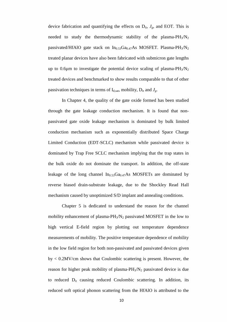
Fig.2.1. Basic experimental set-up for charge pumping measurement [35]……......24
Fig.2.2. Illustration of charge pumping effects by varying the Vg (a) in inversion (b)
in accumulation on a MOSFET [36]…………………..……………………………25
Fig.2.3. Space Charge limited current voltage characteristics for single set of traps
containing trap free and shallow traps [44]……………………………….…….......29
Fig.2.4. Schematic energy band diagrams of Frenkel Poole emission [45]…….......31
Fig.2.5. MBE growth of p-In0.53Ga0.47As on InP with the specifications provided.
In0.53Ga0.47As is 500nm thick, lattice matched with InP…………………………...33
Fig.2.6. Process flow of long channel In0.53Ga0.47As N-MOSFET fabrication….....36
Fig.2.7. Top view of a ring shape In0.53Ga0.47As MOSFET, fabricated using a two-
mask step……………………………….…………………………………………..36
Fig.2.8. Schematic cross section of the self-aligned In0.53Ga0.47As N-MOSFET
integrated with CVD HfAlO gate dielectric and TaN metal gate………………….37
Fig.2.9. Process flow of sub-2µm short channel In0.53Ga0.47As N-MOSFET
fabrication. Words in bold highlight the steps that differ from long channel
In0.53Ga0.47As NMOSFET fabrication process…………………………..................37
Fig.3.1. Cgc curves, generated from split C-V measurement technique, measured at
100kHz of plasma-PH3/N2 passivated devices as a function of temperatures at 600°C
N2 1min, 700°C N2 1min and 800°C N2 5s. Note the 2 order increase in Jg after high
temperature anneal…………………………………………………..………………46
Fig.3.2. TEM images of HfAlO/plasma-PH3/N2 passivated In0.53Ga0.47As gate stack
with (a) no activation anneal but with FGA 400°C (b) 600°C 1min activation anneal
with FGA 400°C and (c) 600°C 1min activation anneal with FGA 400°C followed
by 800°C anneal 5s. (d) Same annealing condition as (c) but showing the good even
HfAlO layer on even In0.53Ga0.47As surface. Note that oxide thickness measured
from TEM is given by ~8nm……………………………..…………………..……48
Fig.3.3. EDX results of HfAlO/PxNy/In0.53Ga0.47As gate stack with 600°C activation
anneal FGA 400°C followed by 800°C anneal at (a) localized rough interface taken

xiii
from Fig.3.2(c) of TEM image and (b) uniform smooth interface taken from
Fig.3.2(d) of TEM image.………..………………………………..………………..49
Fig.3.4. Comparison of the Dit of plasma-PH3/N2 passivated devices which have
undergone annealing conditions at 600°C N2 1min, 700°C N2 1min and 800°C N2 5s.
………………………………………………..…………………….……………....51
Fig.3.5. Maximum transconductance (Gm) which is normalized with gate width of
65μm, for plasma-PH3/N2 passivated and non-passivated devices, which have
undergone annealing conditions at 600°C N2 1min, 700°C N2 1min and 800°C N2
5s (only for plasma-PH3/N2 passivated devices).………………………………..52
Fig.3.6. Subthreshold slope taken at Vd=0.05V which is normalized with gate
width of 65μm, for plasma-PH3/N2 passivated and non-passivated devices, which
have undergone annealing conditions at 600°C N2 1min, 700°C N2 1min and
800°C N2 5s (only for plasma-PH3/N2 passivated devices).…………………….52
Fig.3.7. Id-Vg characteristics of the PxNy-passivated TaN/HfAlO/In0.53Ga0.47As
MOSFET with Lg=600nm, showing maximum Gm of 310mS/mm……………..…..53
Fig.3.8. Id-Vd of 600nm gate length In0.53Ga0.47As MOSFET with plasma-PH3/N2
passivation…………………………………………...…………………………..….53
Fig.3.9. Mobility benchmarking with various passivation techniques including this
work…………………………………………………………………………………54
Fig.3.10. Dit (taken at E-Ei=0.25eV) as a function of EOT for devices with different
passivation or bi-layer gate oxide. …………………………………………….........55
Fig.3.11. Summary of drain current of representative work on In0.53Ga0.47As
MOSFETs, taken at Vd =1V, Vg–Vt,sat =1.5V…………………………….…..…….58
Fig.3.12. Benchmarking of gate leakage current density, Jg, at Vfb+1V for MOSFETs
for this work and other passivation techniques from literature………………..……59
Fig.4.1. Id-Vg characteristics of (a) plasma-PH3/N2 passivated In0.53Ga0.47As N-
MOSFET as a function of temperature. Ideal Vth at 300 K is -0.098 V and (b) non-
passivated In0.53Ga0.47As N-MOSFET as a function of temperature. Ideal Vth at 300 K
is -0.096 V……………………………………………………………………..........65
Fig.4.2. Four-terminal Id-Vg measurements on plasma-PH3/N2 passivated
In0.53Ga0.47As N-MOSFET showing Ioff dominated by Ibulk, known as reverse biased
drain-substrate junction leakage. ……………………………………………..........68
Fig.4.3. Temperature dependence of substrate current (Ibulk) of both plasma-PH3/N2
passivated and non-passivated In0.53Ga0.47As N-MOSFET taken from temperatures
between 300K to 250K. The Ibulk values have been taken at Ioff values at Vg=-0.7V
from Fig.4.1(a) and 4.1(b). An activation energy of Eg/2 extracted in Region (I)
confirms SRH generation-recombination current………………………………....68
Fig.4.4. ln|Id| vs ln|T| plot of both plasma-PH3/N2 passivated and non-passivated
In0.53Ga0.47As N-MOSFET showing a negative temperature dependence of the on-
current……………………………………………………………...…………….....70
xiv
Fig.4.5. (a) HR-TEM image of non-passivated N-MOSFET and (b) HR-TEM image
of plasma-PH3/N2 passivated In0.53Ga0.47As N-MOSFET……………...……………71
Fig.4.6. Jg characteristics of plasma-PH3/N2 passivated and non-passivated
In0.53Ga0.47As N-MOSFET at 300 K. Inset shows the lnǀJgǀ vs lnǀEǀ plot. EOT value of
non-passivated In0.53Ga0.47As N-MOSFET is 1.9 nm and EOT value of passivated
In0.53Ga0.47As N-MOSFET is 1.7 nm. The voltage boundaries and s values of JVs
fits are also shown……………………………………………..............................…73
Fig.4.7. EOT vs physical oxide thickness of both passivated and non-passivated
devices…………………………………………………………………………........74
Fig.4.8. ln|Jg| vs ln|E| plot of non-passivated device at temperatures between 250K
and 420K. Inset shows the Arrhenius plot in the TFL regime……………………...78
Fig.4.9. ln(Jg/E) vs E½ plots (FP fitting) observed in non-passivated In0.53Ga0.47As N-
MOSFET. Inset shows the Arrhenius plot in the FP emission regime………….….78
Fig.4.10. ln|Jg| vs ln|E| plot of plasma-PH3/N2 passivated In0.53Ga0.47As N-MOSFET
at temperatures between 250K and 420K………...………………………………....79
Fig.5.1(a) C–V response at 100kHz with varying temperature of 250K to 420K of
plasma-PH3/N2 passivated HfAlO/In0.53Ga0.47As N-MOSFET. Inset (a) shows
corresponding room-temperature C–V variation between 10kHz to 1MHz in
passivated In0.53Ga0.47As devices and (b) C–V response at 100kHz with varying
temperature of 250K to 420K of non-passivated HfAlO/In0.53Ga0.47As N-MOSFET.
Inset (b) shows corresponding room-temperature C–V variation between 10kHz to
1MHz in non-passivated In0.53Ga0.47As devices………………………………….…88
Fig.5.2. Effective electron mobility in non-passivated and plasma-PH3/N2 passivated
HfAlO/In0.53Ga0.47As N-MOSFET at various temperatures from 250K to 420K, using
the C-V correction method…………………………….……………………...…….90
Fig.5.3. Energy distribution of Dit as determined by the tr and tf dependence of
charge pumping currents. The horizontal lines represent the mean Dit of the entire
bandgap, for non-passivated and plasma-PH3/N2 passivated device………..…..…..92
Fig.5.4. XPS spectra for the In0.53Ga0.47As surfaces with and without plasma-PH3/N2
passivation treatment are shown for (a) As 3d. Typical results of deconvolution
analysis are illustrated with the corresponding chemical bonds indicated [21]…….93
Fig.5.5. Vfb vs EOT plots of passivated and non-passivated In0.53Ga0.47As N-
MOSFETs…………………………………………………………………………...94
Fig.5.6. µeff, µcoul, µph, µsr, for passivated and non-passivated device obtained using
Matthiessen‘s rule………………..……………………………………………….…97
Fig.5.7. Phonon scattering rate vs Temperature for passivated and non-passivated
devices, with difference between both phonon scattering rates being contributed by
the SO phonon scattering caused by HfAlO in the non-passivated
device………………………………………………………………………….…...100
Fig 5.8. Ga 3d and In 4d(a) XPS spectra for the In0.53Ga0.47As surfaces without and
(b) with plasma-PH3/N2 passivation treatment are shown……………..………….102
xv
Fig.5.9. XPS analysis showing P1/P2 ratio as a function of conditions (with and
without PDA) applied to the samples………………………………………..…….103
Fig.6.1(a) Comparison between the experimental and simulated Id-Vg characteristics
of 4µm gate length non-passivated In0.53Ga0.47As MOSFET and (b) Comparison
between the experimental and simulated Id-Vg characteristics of 4µm gate length
plasma-PH3/N2 In0.53Ga0.47As MOSFET…..…………………………………….....113
Fig.6.2. Dit distribution, with trap energy level with respect to the intrinsic Fermi
level, of HfO2/ In0.53Ga0.47As MOSFET with and without plasma-PH3/N2 passivation
simulated for Id-Vg fitting. Only the upper half of the bandgap is shown for fitting
since the simulation results for surface channel architecture MOSFETs are sensitive
to this part of the bandgap only [11]. Note that traps above the CNL are defined as
acceptor-like traps while traps below this level are defined as donor-like
traps……………………………………………….…………………………...…..116
Fig.6.3. Calibration of non-passivated Lg=95nm with 10nm thick HfO2 device
showing matching to the experimental results. Expected performance enhancement
prediction through plasma-PH3/N2 passivation using simulation is also
shown………………………………………………………………...…………….116
Fig.6.4(a) Energy band diagram showing the conduction band energy, Fermi level
energy and valence band of non-passivated and (b)plasma-PH3/N2 passivated device
taken at Vg=-0.5V, Vd=0.05V. The upper and lower black lines correspond to Ec and
Ev respectively while horizontal line between Ec and Ev corresponds to
EF……………………………………......................................................................119
Fig.6.5 (a) Energy band diagram of non-passivated and (b) plasma-PH3/N2
passivated device before reaching strong inversion. Note that Vg is taken at -0.036V
for non-passivated corresponding to Id=0.1µA/µm from Fig.6.1(a) and Vg at taken at
-0.2V for passivated corresponding to Id=0.1µA/µm from
Fig.6.1(b)………......................................................................................................120
Fig.6.6 (a) Energy band diagram of non-passivated and (b) plasma-PH3/N2
passivated device at the respective Vth. Note that Vg is taken at 0.1V for non-
passivated device and Vg is taken at -0.12V for passivated
device..…………..………………………………………………………………...121
Fig.6.7 (a) Distribution of acceptor-like trap density used in three simulations of
Fig.6.7(b). The simulations have been varied such that acceptor-like traps, which
correspond to energy trap levels beyond CNL, are increasing while the donor-like
traps corresponding to energy trap levels below CNL are fixed. ………………....122
Fig.6.7 (b) MEDICI simulation of In0.53Ga0.47As MOSFET with varying acceptor-
like interface traps and fixing donor-like traps, with Dit distribution shown in
Fig.6.7(a). Acceptor-like traps increase Vth and on-current. On current is degraded
from 112 µA/µm to 105µA/µm and 97µA/µm, and Vth increases from 0, 0.02V to
0.1V, for Dit distribution given as simulation 1,2, 3 respectively shown in Fig.6.7(a).
……………………………………………………………………………………..123
Fig.6.7 (c) Distribution of donor-like trap density in three simulations of Fig.6.7(d)
variation. The simulations have been varied such that donor-like traps, which
correspond to energy trap levels below CNL, are increasing while the acceptor-like
traps corresponding to energy trap levels above CNL are fixed.............................123

xvi
Fig.6.7 (d) MEDICI simulation of In0.53Ga0.47As MOSFET with varying donor-like
interface traps and fixing acceptor-like traps with Dit distribution shown in
Fig.6.7(c). Donor-like traps change SS and off current of the device, keeping on-
current unchanged. ……….…………………………………………………........124
Fig 6.8. Comparison of DIBL and subthreshold slope as a function of gate length for
non-passivated vs plasma-PH3/N2 passivated, where EOT of non-passivated device is
3.2nm and passivated device is 3nm taken from the reported data [3]. The SS has
been taken at Vd=1V……………………………………………………………….126
Fig.6.9. Comparison of Vt,sat vs Lg for the two types of devices with scaling metrics
at 1µA/µm…………………………………………………………………..……..126
Fig.6.10. Comparison of Id,sat vs Lg for the two types of devices at Vd=1V, Vg=1V,
where EOT of non-passivated device is 3.2nm and passivated device is 3nm taken
from the reported data [8]..………………………………………………………...127
Fig.7.1. 1D Doping profile for the extension, SD and halo implants by taking a
vertical cut at the S/D.……………………………………………………..………133
Fig.7.2 (a) Id-Vg plot for plasma-PH3/N2 passivated Lg=70nm device with and
without halo implant and (b) Id-Vg plot in linear scale for plasma-PH3/N2 passivated
device with and without halo implant. For devices with halo implant, the peak
concentration is given by 7.2x10¹⁷
cm-3
and 2x10¹⁸
cm-3
……………………..........134
Fig.7.3. 2D potential contours at Vg=0V and Vd=0.7V, for Lg=70nm (a) with halo
implant (7.2x10¹⁷
cm-3
) and (b) with halo implant (2x10¹⁸
cm-3
) and (c) without halo
implant……………………………………………………………………………..135
Fig.7.4. Conduction band energy profile as a function of distance along the channel
taken at 1nm below the PxNy/In0.53Ga0.47Asinterface for Vd=0.7V at Vg=0V.
……………………………………………………………………………………..135
Fig.7.5. Simulation 2D BTBT generation contours at Vg=-0.3V and Vd=0.7V, for
Lg=70nm (a) with halo implant (7.2x10¹⁷
cm-3
) and (b) with halo implant
(2x10¹⁸
cm-3
)…………………………………………………………..…………....136
Fig.7.6. Band diagram in the lateral direction for plasma-PH3/N2 passivated
In0.53Ga0.47As MOSFETs with two different halo implant conditions, taken at
Vg=-0.3V, Vd=0.7V at maximum BTBT generation point. From 1D profile,
maximum BTBT generation occurs at x=3.6µm, y=0.01µm for Fig.7.5(a) and at
x=3.6µm, y=0.004µm for Fig.7.5(b)………………………………………………137
Fig.7.7. 2D plots of the (a) Implanted S/D MOSFET and (b) Raised S/D MOSFET
used in the simulation……………………………………………………..……….138
Fig.7.8. Inversion electron concentration at 1nm below PxNy/In0.53Ga0.47As interface
taken along the channel direction at Vg-Vt,sat=0.5V, Vd=0.7V, for Lg=50nm for
EOT=0.6nm……………………………………………………………….……….140
Fig.7.9. Average electron velocity along the channel of the In0.53Ga0.47As MOSFET
taken at 1nm below PxNy/In0.53Ga0.47As interface and at Vg-Vt,sat=0.5V, Vd=0.7V for
Lg=50nm, EOT=0.6nm…………………………………………………………….140
Fig.7.10. Channel length and EOT dependences of Id,sat and CV/I shows far better
xvii
performance of RSD over conventional ISD. Id,sat taken at Vd=0.7V,Vg-Vt,sat=0.5V
……………………………………………………………………………………..142
Fig.7.11 (a) Comparison of inversion electron concentration between RSD and ISD
MOSFETs, where Lg=50nm, Vg-Vt,sat=0.5V and Vd=0.7V and (b) Comparison of
average electron velocity between RSD and ISD MOSFETs, where Lg=50nm,
Vg-Vt,sat=0.5V and Vd=0.7V………………………………………………...…….143
Fig.7.12. Plot of Vt,sat and DIBL vs Lg for RSD and conventional ISD structures
showing reasonable DIBL for RSD at 50nm…………………………………........144
Fig.7.13. 2D potential contour plot of (a) RSD In0.53Ga0.47As MOSFET and (b) ISD
In0.53Ga0.47As MOSFET for Lg=50nm taken at Vg=0V, Vd=0.7V. ………………..145
Fig.7.14. Conduction band energy profiles for RSD In0.53Ga0.47As MOSFET and ISD
In0.53Ga0.47As MOSFET for Lg=50nm taken at Vg=0V, Vd=0.7V and taken at 1nm
below the interface………………………………………………………………...145
Fig.7.15. Electron flowlines for (a) RSD In0.53Ga0.47As MOSFET and (b) ISD
In0.53Ga0.47As MOSFET for Lg=50nm taken at Vg=0V, Vd=0.7V. Electron flowlines
in (a) do not start from within the spacer at the source unlike in (b)………….......146
Fig.7.16. Plot of SS and Ion /Ioff ratio vs Lg for RSD and ISD N-MOSFETs………146
Fig.7.17. Electron density distribution in the inversion layers for In0.53Ga0.47As bulk
and thin channel MOSFET for Lg=40nm at EOT=0.6nm. Note that 0.03µm
corresponds to the PxNy/In0.53Ga0.47As interface and vertical distance from surface
refers to distance away from PxNy/In0.53Ga0.47As interface. Plot has been taken at the
center of the channel……………………………………………………………….147
Fig.7.18. Channel length and EOT dependences of Id,sat shows better performance of
thin channel In0.53Ga0.47As MOSFET over bulk channel…………………………..148
Fig.7.19 (a) Inversion electron concentration along the channel for thin
channel=10nm structure for Lg=50nm, Vg-Vt,sat=0.5V and Vd=0.7V at EOT=0.6nm
and (b) Inversion electron concentration along the channel for bulk structure for
Lg=50nm, Vg-Vt,sat=0.5V and Vd=0.7V at EOT=0.6nm…………………………..150
Fig.7.20 (a) Average electron velocity along the channel for thin channel=10nm
structure for Lg=50nm, Vg–Vt,sat=0.5V and Vd=0.7V at EOT=0.6nm and (b) Average
electron velocity along the channel for bulk structure for Lg=50nm, Vg-Vt,sat=0.5V
and Vd=0.7V at EOT=0.6nm………………………...………………….…..…….151
Fig.7.21. Plot of Vt,sat and DIBL vs Lg for thin channel and bulk In0.53Ga0.47As
MOSFET………….……………………………………………………………….152
Fig.7.22 Plot of SS and Ion /Ioff ratio vs Lg for RSD bulk and thin channel
MOSFETs………………………………………………………………………….152
Fig.7.23 Device design of the structure simulated…………………..…………….154
Fig.7.24. Id-Vg plot as a function of channel thickness for Vd=0.7V at fixed Ioff of
0.1µA/µm………………………………………………………………………….156
Fig.7.25. Electron density distributions in the inversion layers computed for UTB

xviii
structures as a function of channel thickness at Vd=0.7V, Vg=0.7V. These profiles
have been extracted at the middle of the channel region……………..…………...156
Fig.7.26. SS and DIBL vs Lg characteristics as a function of channel thickness….157
Fig.7.27. Potential contours for Lg=22nm with (a) Tch=12nm and (b) Tch=3nm......157
Fig.7.28. Conduction band energy vs distance along the channel comparing
Tch=12nm and Tch=3nm for Lg=22nm device……………………………………...158
Fig.7.29 Three different spacer material used on the In0.53Ga0.47As MOSFET
structures with Tch=3nm simulated with (a) Si3N4 spacer (b) HfO2 extended to
regions below spacer (c) HfO2 spacer……………………………………………..159
Fig.7.30. Id-Vg characteristics showing DIBL and GIDL with comparison with the 3
types of spacer material……………………………………………………………160
Fig.7.31. 2D electric field plot taken at Vg=-0.3V, Vd=0.7V comparing the structure
with three different spacer materials with (a) Si3N4 spacer (b) HfO2 extended to
regions below spacer (c) HfO2 spacer……………………………………………..160
Fig.7.32. Electric field contours taken at 1nm below the PxNy/In0.53Ga0.47As interface
at the region along the channel with Vg=-0.3V and Vd=0.7V. Here the electric field
taken from Fig.7.31(a), especially at the region of the channel/drain interface, shows
the most focused and abrupt field while the electric field taken from Fig.7.31(c)
shows a laterally spread field which is responsible for its smaller
GIDL…...................................................................................................................161
Fig.7.33. Id–(Vg-Vth) plot for (a) Vd=0.7V and Vd=0.05V, for Lg=22nm devices with
and without heterostructure in log scale and (b) Vd=0.7V and Vd=0.05V, for
Lg=22nm devices with and without heterostructure in linear
scale……………………………………………………………..………………...164
Fig.7.34. Electrostatic integrity as a function of gate length for device with and
without heterostructure. Heterostructure device shows slightly worse SCE compared
to without heterostructure……………………...……………………………….…167
.
Fig.7.35. SS and Ion/Ioff a function of gate length for device with and without
heterostructure……………………………………………………………………..167
Fig.7.36. Id,sat and CV/I plots for device without heterostructure as a function of Lg
with Id,sat taken at Vd=0.7V, Vg-Vt,sat=0.5V………………………………..……....168
Fig.7.37. Plot of Vt,sat and Id,sat as a function of Lg for Vd=0.7V, Vg-Vt,sat=0.5V. Lg
below 50nm shows the region where the electrostatic effect from the drain becomes
significant, resulting in significant roll off as well as causing reduced drive current
with scaling…………………………………………………………………….…..168
Fig.7.38 (a) Id-Vg plot of device without heterostructure for Lg=14nm, 22nm and
28nm taken at Vd=0.7V and (b) Linear scale plot of Id-(Vg-Vt,sat) for device without
heterostructure for Lg=14nm, 22nm and 28nm taken at Vd=0.7V…………………169

xix
Fig.7.39 (a) Id-Vg plot of device with heterostructure for Lg=14nm, 22nm and 28nm
taken at Vd=0.7V and (b) Id-(Vg-Vt,sat) plot of device with heterostructure for
Lg=14nm, 22nm and 28nm taken at Vd=0.7V…………………………..................170

xx
List of Symbols and Acronyms
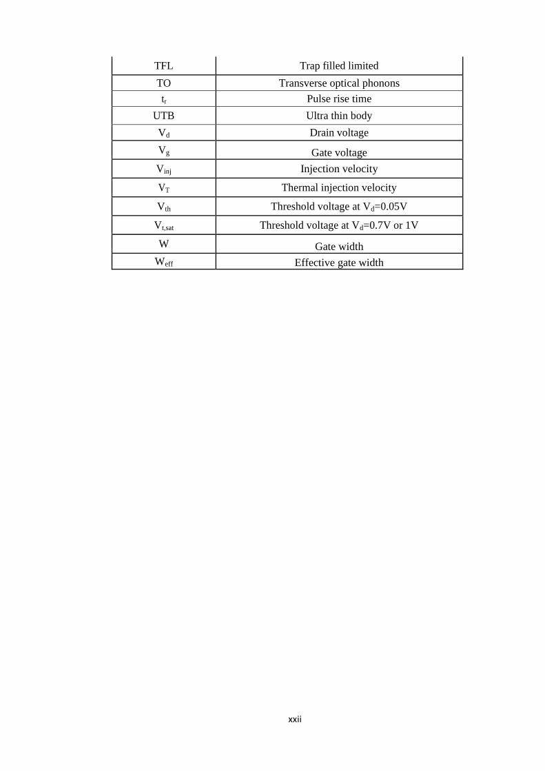
Symbol /Acronym Description
ALD Atomic Layer Deposition
B Ballistic coefficient
BTBT Band to band tunneling
CBM Conduction band minima
CD Depletion capacitance
Cg Gate capacitance
Cgc Gate-to-channel capacitance
Cit Interface trap capacitance
Clf Low frequency capacitance
CNL Charge Neutrality Level
Cox Gate oxide capacitance
CP Charge pumping
Cs Semiconductor capacitance
DIBL Drain Induced Barrier Lowering
Dit Interface trap density
DOS Density of states
Ea Activation energy
r Dynamic dielectric constant
EBL Electron beam lithography
Ec Conduction band minima
EDT SCLC Exponentially distributed trap SCLC
EDX Energy Dispersion X-Ray
EF Fermi energy level
Ei Intrinsic fermi level
EOT Equivalent oxide thickness
Et Trap energy level
FN Fowler-Nordheim
FP Frenkel Poole
GGO Gallium-Gadolinium Oxide
Gm Maximum transconductance
HCl Hydrochloric
Id,sat Saturation drive current
Ion On-current
ISD Implanted Source/Drain

xxi
k Permittivity
Jg Gate leakage current density
λ Correlation length
Lg Gate length
LO Longitudinal optical phonons
m* Effective mass
MBE Molecular beam epitaxy
MLD Mono-layer Doping
MOCVD Metal-Organic-Chemical-Vapor-Deposition
µeff Effective mobility
µcoul Mobility limited by coulombic scattering
µph Mobility limited by phonon scattering
µsr Mobility limited by surface roughness scattering
(NH4)2S Wet sulfide
Ninv Inversion electron concentration
Nt Average trap concentration
PECVD Plasma enhanced chemical vapour deposition
PVD Physical vapour deposition
PxNy Phosphorus nitride
Qinv Inversion charge density
r Backscattering rate
Rc Contact resistance
RMS Root mean square
RSD Raised Source/Drain
Rsh Sheet resistance
SCLC Space Charge Limited Conduction
SCE Short channel effect
S/D Source/Drain
SE Schottky Emission
SO Soft optical
SS Subthreshold Slope
TMA trimethyl aluminum
CV/I Gate delay
τc Carrier transit time
τd Dielectric relaxation time
Tch Channel thickness
tf Pulse fall time
xxii
TFL Trap filled limited
TO Transverse optical phonons
tr Pulse rise time
UTB Ultra thin body
Vd Drain voltage
Vg Gate voltage
Vinj Injection velocity
VT Thermal injection velocity
Vth Threshold voltage at Vd=0.05V
Vt,sat Threshold voltage at Vd=0.7V or 1V
W Gate width
Weff Effective gate width

1
Chapter 1: Introduction and Motivation
1.1. Silicon transistor scaling: Benefits and Issues
Moore‘s Law predicted that the number of transistors placed on an
integrated circuit (IC) would double every two years [1] and has been
known to guide the progress. The device scaling is the key attribute for
planar MOSFET circuitry in order to achieve significantly higher packing
density per unit chip area, reduction of cost per function and improvement
in circuit speed performance.
The key concept of the MOSFET scaling proposed by Dennard in
1974 [2] is that various structure and electrical parameters of MOSFET
should be scaled simultaneously, which guarantees the reduction in device
dimensions without compromising the current-voltage characteristics.
However, as MOSFET continues to scale down to sub-100nm, the
conventional device scaling is confronted with several limitations, which
provide the trade-off relationships among on-current, power consumption
and short channel effects as shown in Fig.1.1. One such example is that to
maintain the on-current scaling with reduced gate length (Lg), oxide
thickness has to be reduced, but this will cause greater power consumption
in terms of high gate leakage current. Also, as Lg is scaled, significant
control of channel by the gate is lost and the drain field begins to influence
the channel formation, resulting in short channel effect (SCE). Hence, new
device engineering methods to overcome these difficulties are much needed
to mitigate the trade-offs.
These new device technologies, shown as possible solutions in Fig.1.1
[3] are known as the technology boosters, and they include technologies or

2
structures such as high-k/metal-gate for gate stack engineering, high carrier
mobility or high carrier velocity channels, ultrathin-body (UTB) structures
and multigate structures for channel engineering and metal source/drain
(S/D) for S/D engineering. The principle of these technology boosters is to
improve the device parameters such as gate leakage current, mobility,
saturation velocity and short channel effects. For instance a 45nm process
technology based on high-k, metal gate, and strained silicon was introduced
in 2000 [4] while scaling of this technology continued to the 32nm
technology node in 2009 [5]. More recently in 2011, FINFET structure was
introduced to enable further scaling to the 22nm technology node [6]. As
technology node progresses towards sub-20nm, fundamental limits of Si
properties and gate pitch will impose limitations to the continuous scaling of
device dimensions in terms of challenges to the conventional techniques and
materials used for CMOS strain engineering. Therefore, future advancement
of CMOS scaling would require novel channel materials, processes and
device architectures.
Fig.1.1. Trade-off factors among on-current, power consumption/leakage
current and short channel effects under simple device scaling and possible
solutions [3].

3
1.2. Motivation of III-V Channel Materials for Future CMOS
applications
When MOSFET is scaled to deep sub-100nm technology node,
carrier transport in the scaled device becomes quasi-ballistic. It has been
shown through simulation and experiments that injection velocity, instead of
saturation velocity, is still a reliable performance indicator for the drive
current [7-10].
Lundstrom’s theory [11] initially pointed out based on scattering
theory that the drain current at the saturation condition is dominated by
thermal injection velocity, VT , at the source side instead of the saturation
velocity, in short channel devices. The saturation current of a short channel
device can be expressed as:
Id,sat=CoxWeffVT((1-r)/(1+r))(Vg-Vth) Equation (1.1)
where Cox is the gate oxide capacitance, Weff is the effective gate width, r is
the backscattering coefficient which indicates the number of carriers
backscattered to the source, Vg is the voltage between the gate and the
source, Vth is the threshold voltage, and VT is the thermal injection velocity.
VT is dependent on low field mobility and r is inversely proportional to low
field mobility [9-10]. For extremely scaled devices operating in the ballistic
regime i.e. r=0, where the ballistic coefficient, B=((1-r)/(1+r))=1, the
maximum current would be controlled by the injection velocity near the
source region of the transistor.
Therefore, by incorporating new channel materials with higher low
field mobility and higher injection velocity near the source region, the
performance of In0.53Ga0.47As in quasi-ballistic regime is expected to be
better than Si. Based on Table 1.1, III-V compound semiconductors have

4
significantly smaller electron effective mass compared to silicon which
leads to high electron mobility that can translate into enhanced device
performance at low supply voltage [12].
Table 1.1. Physical parameters of the commonly used semiconductors as
channel materials [12].
1.3. Challenges of III-V CMOS Technology
In order to reap the advantages of the intrinsic properties of III-V
materials, a lot of challenges still have to be overcome before the
manufacturing of III-V logic transistors becomes viable [12]. Such
challenges include cost effective heterogeneous integration of III-V on Si,
formation of thermally stable gate dielectric with low interface state density
and leakage and realization of S/D with low resistance. Fig.1.2 summarizes
the challenges faced by III-V CMOS [13] and some will be briefly
discussed in the subsequent sections.

5
Fig.1.2. Schematic illustration showing the technical challenges faced by high
mobility III-V CMOS on Si substrates for future logic applications [13].
1.3.1. Formation of High Quality and Thermodynamically Stable
Gate Stack for InxGa1-xAs N-MOSFETs
As disussed in previous sections, significant increase in carrier
injection velocity is crucial in order to maintain the commensurate
performance scaling of MOSFETs to the gate length. Hence, to take
advantage of the electronic transport properties of III-V NMOS, in
particular In0.53Ga0.47As MOSFET in this work, researchers are exploring
for thermodynamically stable gate dielectrics which can form unpinned
Fermi level at the In0.53Ga0.47As oxide interface [14-28] since a decade ago.
In order to realize high performance In0.53Ga0.47As N-MOSFET a
high quality and thermodynamically stable high-k gate stack on
In0.53Ga0.47As is needed. However, when the surface is oxidized during
high-k oxide deposition, a high density of interface states which include
different native surface species caused by oxygen related reaction (Ga–O
bonds, As–O bonds), interfacial lattice defects and stoichiometry
perturbation such as As-As, elemental As, and As and Ga anti-sites can be
formed [29-30]. Unlike SiO2 on Si, the native oxides of In0.53Ga0.47As can
generate high density of interface states which can cause Fermi level

6
pinning, resulting in an increased subthreshold swing, frequency dispersion
of capacitance, electron mobility degradation and creating reliability issues.
In order to reduce interface trap density (Dit) and unpin the
In0.53Ga0.47As interface, various techniques have been studied which include
in-situ molecular beam epitaxy (MBE) growth of gallium-gadolinium oxide
(GGO) [31], metal organic chemical vapour deposition (MOCVD) of
HfAlO and HfO2 with SiH4, NH3 or plasma-PH3/N2 treatment [26-27],
atomic layer deposition (ALD) of Al2O3, HfO2, ZrO2, La(AlOx)/ZrO2 and
TaSiOx [32-39] using silicon or InP capping layer [40-42]. Note that most
methods employed do not involve high-k dielectric forming directly on
In0.53Ga0.47As, which has the disadvantage of high Dit formation between the
high-k dielectric and In0.53Ga0.47As, and thus can result in significant carrier
scattering and mobility degradation. Nevertheless, all the reported Dit values
on various MOS devices are still higher than 1x10¹¹
cm-2
eV-1
[12] resulting
in low electron mobility observed in inversion layer of In0.53Ga0.47As N-
MOSFET. Further reduction of Dit is still desirable.
One technique employed, other than passivation technique, to
improve the mobility and hence device performance of In0.53Ga0.47As
MOSFET is to bury the channel beneath a wide bandgap material (known as
capping layer), thus separating the charged interface states from the channel
causing reduced Coulombic scattering and remote phonon scattering from
oxide phonons. However, one disadvantage of this technique is the electron
spillover from the channel to the capping layer, thus reducing the mobility
in the high E-field. In addition, this technique may not provide good
scalability as device scales due to its larger capacitance equivalent thickness
(CET) caused by the presence of low-k capping layer. Also, the mobility of

7
the device would not only be dependent on the capping layer/InxGa1-xAs
channel interface but also on the high-k/capping layer interface [43] which
requires sufficiently low Dit and hence surface channel MOSFET studies
involving such high-k/capping layer interface are still necessary.
Not only reduced Dit is important, thermally stable high-k dielectric
is also required to ensure that the interface between high-k and
In0.53Ga0.47As maintains its high quality even after subsequent thermal
process steps which include S/D dopant activation anneal of between
600°C-800°C.
1.3.2. Channel Engineering
Due to their significant transport advantage which allows high
performance even at low supply voltage, high mobility materials are being
very actively researched as channel materials for future highly scaled
CMOS. However the device design considerations for In0.53Ga0.47As
MOSFET differ from that of a Si MOSFET. This is due to the fact that most
explored high mobility materials have a significantly smaller bandgap
compared to Si, leading to very high band-to-band tunneling (BTBT)
leakage currents, which may limit their scalability. In addition, since most
high mobility materials also typically have a higher permittivity (k), they
also suffer from worse short channel effects (SCEs). Thus the off-state
leakage and SCE of In0.53Ga0.47As MOSFETs is expected to be of worse
performance compared to Si MOSFETs. In addition, the driving capability
of In0.53Ga0.47As MOSFETs may also be adversely affected because of their
much smaller density of states (DOS) due to its small effective mass

8
compared to silicon. Small DOS affects the device performance in terms of
the loss of inversion capacitance which limits the transconductance and the
reduction in scattering rate in the source of the MOSFET which limits the
ability of the source to sustain a sufficiently large flow of carriers into the
channel. The latter phenomenon is known as source starvation. In addition,
when large gate electric field is applied, electrons filling up the Г valley
would tend to move to the L valley as well where the effective mass
increases and mobility drops [44-45]. Hence, the preferred InxGa1-xAs alloy
is one with larger energy level difference between different Г-L valleys but
also with acceptable conduction band DOS [46-47].
1.3.3. Formation of Ultrashallow Junctions With Low S/D
Resistance
In addition to the gate stack, selection of the best ohmic contact and
junction technology is also important. Implanted junctions that have served
silicon well may not be suitable for compound semiconductors due to the
compound nature of In0.53Ga0.47As which can result in lower maximum
activated doping density, loss of stoichiometry due to preferential group V
evaporation and difficulty in recovering from implant amorphization.
A number of alternatives are being studied to replace implantation as
the junction technology of source. One example of a promising approach is
selective regrowth, where either MBE or MOCVD is used to selectively
regrow very heavily doped S/D regions [48-49]. Advantages of such
approach over implantation include 1) abrupt doping profile 2) reduced
drain junction leakage current, which controls the device off-state leakage,
caused by the absence of implantation damage and 3) high doping density.
9
This can provide low access resistance (in addition to low contact
resistance) and reduces the junction leakage which tends to become
significant due to its smaller bandgap than silicon, hence addressing the
issues related to device scalability as device approaches deep sub-100nm
technology node.
Other techniques pursued to create a potentially defect-free S/D is
the use of silicide like process involving selective epitaxy of GeSi on N+
In0.53Ga0.47As with two step metallization process [50-51] and monolayer
doping (MLD) through the use of sulphur [52].
1.4. Thesis outline
The focus of this thesis would be addressing the three challenges of
InxGa1-xAs MOSFETs described in previous sections. The issues in Sections
1.3.1 is addressed in Chapters 3-6. The issues in Sections 1.3.2-1.3.3 will be
addressed in TCAD simulation Chapter 7. The main technical contributions
would be documented into 6 chapters as shown below.
Chapter 2 consists of an overview of passivation techniques on
In0.53Ga0.47As and description on charge pumping technique for interface
trap characterization. In addition, an overview of the gate leakage
mechanisms used in this work as well as insights on new mobility scattering
mechanisms, more specific to In0.53Ga0.47As MOSFETs obtained from this
work, are summarized. Also, process flows for the long channel and short
channel device fabrication have been included.
In Chapter 3, the robustness of the high-k/In0.53Ga0.47As with
plasma-PH3/N2 treatment with high temperature annealing has been studied
by varying annealing temperature from 600°C to 800°C after completion of
10
device fabrication and quantifying the effects on Dit, Jg, and EOT. This is
needed to study the thermodynamic stability of the plasma-PH3/N2
passivated/HfAlO gate stack on In0.53Ga0.47As MOSFET. Plasma-PH3/N2
treated planar devices have also been fabricated with submicron gate lengths
up to 0.6µm to investigate the potential device scaling of plasma-PH3/N2
treated devices and benchmarked to show results comparable to that of other
passivation techniques in terms of Id,sat, mobility, Dit and Jg.
In Chapter 4, the quality of the gate oxide formed has been studied
through the gate leakage conduction mechanism. It is found that non-
passivated gate oxide leakage mechanism is dominated by bulk limited
conduction mechanism such as exponentially distributed Space Charge
Limited Conduction (EDT-SCLC) mechanism while passivated device is
dominated by Trap Free SCLC mechanism implying that the trap states in
the bulk oxide do not dominate the transport. In addition, the off-state
leakage of the long channel In0.53Ga0.47As MOSFETs are dominated by
reverse biased drain-substrate leakage, due to the Shockley Read Hall
mechanism caused by unoptimized S/D implant and annealing conditions.
Chapter 5 is dedicated to understand the reason for the channel
mobility enhancement of plasma-PH3/N2 passivated MOSFET in the low to
high vertical E-field region by plotting out temperature dependence
measurements of mobility. The positive temperature dependence of mobility
in the low field region for both non-passivated and passivated devices given
by < 0.2MV/cm shows that Coulombic scattering is present. However, the
reason for higher peak mobility of plasma-PH3/N2 passivated device is due
to reduced Dit causing reduced Coulombic scattering. In addition, its
reduced soft optical phonon scattering from the HfAlO is attributed to the

11
thicker ~0.6nm thick and robust passivation layer, known as PxNy layer, of
the passivated device compared to the ~0.35nm thick interfacial layer of
non-passivated device. In addition to reduced surface roughness scattering,
the reduced interface dipole scattering is attributed to the ~0.6nm thick
robust passivation layer which prevents interdiffusion of In/Ga across the
interface resulting in less randomly oriented dipoles. Thus these reduced
soft optical phonon scattering and reduced surface roughness and interface
dipole scattering contributed to the higher mobility in mid to high E-field
region respectively.
Chapter 6 involves TCAD simulation with calibration parameters
being carried out to match data from previous IEDM 2008 published works
from our group. The aim of this TCAD study is to: 1) confirm that the larger
Vth for non- passivated device is caused by larger concentration of acceptor-
like traps as observed from our experimental results in Chapter 4 2) confirm
the reason for larger Ioff is due to its larger concentration of donor-like traps,
as explained from the energy band-diagram and its relation to the Dit which
affect the Id-Vg plots and 3) investigate the performance scalability of
In0.53Ga0.47As MOSFET with and without passivation for Lg up till 60nm for
the current process flow used by our group.
Chapter 7 also involves TCAD simulation, with similar calibration
parameters used in Chapter 6, but with device optimization of plasma-
PH3/N2 passivated In0.53Ga0.47As MOSFET by changing the original process
flow or device dimension. This is done through (a) reduced gate to S/D
contact spacing to 15nm, by adding spacer of width 15nm, from 2µm in the
original process flow (b) reduced contact resistance to 400Ω.µm achievable
in implanted S/D In0.53Ga0.47As MOSFET, compared to 1200Ω.µm in the

12
original process flow (c) Addition of halo implant. To counteract the trade-
off between electrostatic integrity and drive current, performance scalability
of raised S/D (RSD) MOSFET is studied and it is found to be beneficial due
to reduced source starvation effect. In order to sustain low SCE up till 14nm
technology node, thin channel with RSD MOSFET, high-k spacer and
structures both with and without heterostructure, has also been studied and
benchmarked with results from other simulation groups.
Chapter 8 would show the general conclusions and suggestions for
future work.
A flow chart of the outline of the thesis which is divided into two
branches dealing with research issues addressed through experimental work
as well as partly TCAD work as shown in Fig.1.3 and TCAD work
involving optimization of device structures as shown in Fig.1.4.

13
Fig.1.3. Flowchart of the issues addressed in high-k/In0.53Ga0.47As MOSFETs in
the first part of the thesis found in Chapters 3-6.
Problem 1: High-k/In0.53Ga0.47As gate stack issue with:
(a) High Dit and nature of traps affecting the Id-Vg plot
(b) Low mobility and low on-state performance
(c) Large gate leakage
(d) Thermal stability at annealing temperature > 600°C for high S/D
activation
Main idea1: Plasma-PH3/N2 passivation treatment on
HfAlO/In0.53Ga0.47As MOSFET
Addresses issue 1(d):
Thermal stability of
passivated device until
800°C (Chapter 3)
Addresses issues 1(a) and 1(b):
(a) Dit at 0.23eV above the intrinsic Fermi level is 2.5x10¹²
cm-2
eV-1
compared to 9x10¹²
cm-2
eV-1
for non-passivated device
(b) Temperature dependence mobility measurements from 250K to
420K show the cause of mobility improvement of passivated device is
due to reduced Coulombic scattering, attributed to reduced free As
caused by the presence of active hydrogen species through volatile As-
H3 bond formation, reduced contribution of soft optical phonon
scattering from the HfAlO as well as reduced interface dipole scattering
caused by reduced Ga/In elemental interdiffusion across interface
(Chapter 5)
(c) Vth improvement for plasma-PH3/N2 passivated device is due to
lesser acceptor-like traps (Chapter 4 and Chapter 6)
Addresses issue 1(c): Lower Gate
leakage at higher temperatures
with smaller temperature
dependence due to absence of
bulk limited conduction i.e.
absence of Frenkel Poole
emission and lower ohmic
conduction current; thus suitable
for gate stack scalability (Chapter
4)

14
Fig.1.4. Flowchart of the issues addressed in high-k/In0.53Ga0.47As MOSFETs in
the second part of the thesis found in Chapter 7.
Problem 2: Short channel In0.53Ga0.47As MOSFETs
(a) Poor electrostatic integrity
(b) Low on-state performance due to source starvation effects and large
S/D parasitic resistance
(c) Performance scalability – Reduced Id,sat with scaling could be caused
by source starvation effects and poor electrostate integrity
(d) Increased BTBT resulting in worsened GIDL
Addresses issue 1(b) and 1(c) (Chapter
7):
(a) RSD MOSFET to reduce source
starvation through larger active dopant
concentration as high as 6.5x10¹⁹
cm-3
compared to 1x10¹⁹
cm-3
for implanted
S/D MOSFET, resulting in 4X reduction
in Rc from 400Ω.µm to 93 Ω.µm
(b) Improve electron concentration near
source with RSD, thin channel MOSFET
caused by electron confinement which
reduces inversion layer width, and
improves electrostatic integrity
(c) Improvement in Id,sat due to improved
low field peak mobility of
heterostructure device compared to non-
heterostructure device.
Addresses issue 1(a)
(Chapter 7):
(a) RSD MOSFET
improved electrostatic
integrity compared to
implanted S/D MOSFET
due to absence of deep S/D
which causes reduced
dopant concentration near
the gate edge
(b) Thin channel up till
3nm needed for 14nm
gate length
Addresses issue 1(d) (Chapter 7):
(a) High-k spacer reduces the peak electric field and causes a more
spread out E-field profile
15
REFERENCES
[1] G.E. Moore, "Cramming more components onto integrated circuits",
Proceedings of the IEEE, Vol. 86, pp. 82-85, 1998.
[2] R. H. Dennard, F. F. Gaensslen, N.-N. Yu, V. L. Rideout, E. Bassous, and A.
R. LeBlanc, "Design of ion-implanted MOSFETs with very small physical
dimensions", IEEE J. Solid-State Circuits, Vol. 9, pp. 256- 268, 1974.
[3] S. Takagi, T. Irisawa, T. Tezuka, T. Numata, S. Nakaharai, N. Hirashita, Y.
Moriyama, K. Usuda, E. Toyoda, S. Dissanayake, M. Shichijo, R. Nakane, S.
Sugahara, M. Takenaka, and N. Sugiyama, "Carrier-transport-enhanced channel
CMOS for improved power consumption and performance", IEEE Trans.
Elec.Dev., Vol. 55, pp. 21-39, 2008.
[4]K. Mistry, C. Allen, C. Auth, B. Beattie, D. Bergstrom, M. Bost, M. Brazier, M. Buehler, A. Cappellani, R. Chau, “A 45 nm logic technology with high-k plus metal gate transistors, strained silicon, 9 Cu interconnect layers, 193nm dry patterning and 100% Pb-free packaging”, Tech. Dig. – Int. Electron Devices Meet, pp. 247, 2007.
[5]S. Natarajan, M.Armstrong, M. Bost, R. Brain, M. Brazier, C.-H. Chang, V. Chikarmane, and M. Childs, “A 32 nm logic technology featuring 2nd-generation high-k plus metal-gate transistors, enhanced channel strain and 0.171 μm
2 SRAM
cell size in a 291 Mb array”, Tech. Dig. – Int. Electron Devices Meet, pp. 941, 2008.
[6]C. Auth, C. Allen, A. Blattner, D. Bergstrom, M Brazier, M. Bost, M. Buehler,
V. Chikarmane, T. Ghani, and T. Glassman,“A 22 nm high performance and low-
power CMOS technology featuring fully-depleted Tri-gate transistors, self-aligned
contacts and high density MIM capacitors”, Symposium on VLSI Technology, pp.
131, 2012.
[7]M. Lundstrom, “Elementary scattering theory of the Si MOSFET”, IEEE
Elec.Dev.Lett., Vol. 18, No. 7, pp. 361, 1997.
[8]M.S. Lundstrom, “On the mobility versus drain current relation for a nanoscale
MOSFET”, IEEE Elec. Dev. Lett., Vol. 22, No. 6, pp. 293, 2001.
[9]S. Takagi, T. Irisawa, T. Tezuka, T. Numata, S. Nakaharai, N. Hirashita, Y.
Moriyama, K. Usuda, E. Toyoda, S. Dissanayake, M. Shichijo, R. Nakane, S.
Sugahara, M. Takenaka, and N. Sugiyama, “Carrier-transport-enhanced channel
CMOS for improved power consumption and performance”, IEEE Trans.
Elec.Dev., Vol. 55, No. 11, pp. 21-39, 2008.
[10]A. Lochtefeld, I.J. Djomehri, G. Samudra, and D.A. Antoniadis, “New insights
into carrier transport in N-MOSFETs”, IBM J.Research and Development, Vol. 46,
pp. 347, 2002.
[11]M. Lundstrom, “Elementary scattering theory of the Si MOSFET”, IEEE
Ele.Dev. Lett., Vol. 18, pp. 361–363, 1997.
[12]S.Oktyabrsky and P.D.Ye, “Fundamentals of III-V semiconductor MOSFETs”,
Springer, New York, 2009.
16
[13]Zhang Xingui, “Self-aligned Source and Drain Contact Engineering for high
mobility III-V Transistor”, PhD dissertation, National University of Singapore,
2013.
[14]F. Ren, M. Hong, W. S. Hobson, J. M. Kuo, J. R. Lothian, J.P. Mannaerts, J.
Kwo, S.N. G. Chu, Y.K. Chen, and A.Y. Cho, “Demonstration of enhancement
mode p- and n-channel GaAs MOSFETs with Ga2O3(Gd2O3) as gate oxide”, Solid
State Electron., Vol. 41, pp. 1751-1753, 1997.
[15]P.T. Chen, Y. Sun, E. Kim, P.C. McIntyre, W. Tsai, M. Garner, P. Pianetta,
Y.Nishi, and C.O. Chui. “HfO2 gate dielectric on (NH4)2S passivated (100) GaAs
grown byALD”, J. Appl. Phys., Vol. 103, p. 034106, 2008.
[16]R.M. Wallace, P.C. McIntyre, J. Kim, and Y. Nishi, “Atomic layer deposition
of dielectrics on Ge and III–V materials for ultrahigh performance transistors”,
MRS Bull., Vol. 34, pp. 493-503, 2009.
[17]M. Houssa, E. Chagarov, and A. Kummel, “Surface defects and passivation of
Ge and III–V Interfaces”, MRS Bull., Vol. 34, pp. 504-513, 2009.
[18]S.Datta, “III-V field-effect transistors for low power digital logic applications”,
Microelectronic.Eng, vol. 84, pp. 2133, 2007.
[19]R.J.W. Hill, C. Park, J. Barnett, J. Price, J. Goel, W.Y. Loh, J. Oh, C.E. Smith,
P. Kirsch, P. Majhi, and R. Jammy, “Self-aligned III-V MOSFETs heterointegrated
on a 200 mm Si substrate using an industry standard process flow”, Tech. Dig. –
Int. Electron Devices Meet., pp. 130, 2010.
[20]D.-H. Kim and J.A. del Alamo, “Logic-performance of 40 nm InAs HEMTs”,
Tech. Dig. – Int. Electron Devices Meet., pp. 629, 2007.
[21]T.-W.KimD.-H.Kim and J.A.del Alamo, “60nm self-aligned-gate In0.53Ga0.47As
HEMTs with record high-frequency characteristics”, Tech. Dig. – Int. Electron
Devices Meet., pp. 696, 2010.
[22]Y.Q. Wu, M. Xu, R.S. Wang, O. Koybasi, and P.D. Ye, “High performance
deep-submicron inversion-mode In0.53Ga0.47As MOSFETs with maximum Gm
exceeding 1.1 mS/μm: new HBr pretreatment and channel engineering”, Tech. Dig.
– Int. Electron Devices Meet., pp. 323, 2009.
[23]Y. Xuan, T. Shen, Y.Q. Wu, and P.D. Ye, “High performance surface channel
In-rich In0.75Ga0.25As MOSFETs with ALD high-k as gate dielectrics”, in Tech.
Dig. – Int. Electron Devices Meet, pp. 371, 2008.
[24]J. Huang, N. Goel, H. Zhao, C. Y. Kang, K.S. Min, G. Bersuker, S.
Oktyabrsky, C. K. Gaspe, M. B. Santos, P. Majhi, P.D. Kirsch, H.-H. Tseng, J.C.
Lee, and R. Jammy, “InGaAs MOSFET performance and reliability improvement
by simultaneous reduction of oxide and interface charge in ALD (La)AlOx/ZrO2
gate stack”, Tech. Dig. – Int. Electron Devices Meet., pp. 335, 2009.
[25]H.-C. Chin, X. Gong, X. Liu, Z. Lin, and Y.-C. Yeo, “Strained In0.53Ga0.47As
N-MOSFETs: performance boost with in-situ doped lattice-mismatched
source/drain stressors and interface engineering”, Symposium on VLSI Technology-
, pp. 244, 2009.

17
[26]J. Lin, S. Lee, H.-J. Oh, W. Yang, G.Q. Lo, D.L. Kwong and D.Z. Chi,
“Plasma PH3-passivated high mobility inversion InGaAs MOSFET fabricated with
self-aligned gate-first process and HfO2/TaN gate stack”, Tech. Dig. – Int.
Electron Devices Meet., pp. 401, 2008.
[27]H.J. Oh, J.Q. Lin, S.A.B. Suleiman, G.Q. Lo, D.L. Kwong, D.Z. Chi, and S.J.
Lee, “Thermally robust phosphorous nitride interface passivation for InGaAs self-
aligned gate first n-MOSFET integrated with high-k dielectric”, Tech. Dig. – Int.
Electron Devices Meet., pp. 339, 2009.
[28]M. Radosavljevic, B. Chu-Kung, S. Corcoran, G. Dewey, M.K. Hudait, J.M.
Fastenau, J. Kavalieros, W.K. Liu, D. Lubyshev, M. Metz, K. Millard, N.
Mukherjee, W. Rachmady, U. Shah, and R. Chau, “Advanced high-k gate dielectric
for high-performance short-channel In0.7Ga0.3As quantum well field effect
transistors on silicon substrate for low power logic applications”, Tech. Dig. – Int.
Electron Devices Meet., pp. 319, 2009.
[29]F. Ren, M. Hong, W.S. Hobson, J.M. Kuo, J.R. Lothian, J.P. Mannaerts,
J.Kwo, S.N.G. Chu, Y.K. Chen, and A.Y. Cho, “Demonstration of enhancement-
mode p and n-channel GaAs MOSFETs with Ga2O3(Gd2O3) as gate oxide”, Solid
State Electron., Vol. 41, pp. 1751-1753, 1997.
[30]S. Koveshnikov, W. Tsai, I. Ok, J.C. Lee, V. Torkanov and M. Yakimov,
“Metal-oxide-semiconductor capacitors on GaAs with high-k gate oxide and
amorphous silicon interface passivation layer”, Appl Phys Lett, Vol.88, pp.022106,
2006.
[31]M.J. Hale, S.I. Yi, J.Z. Sexton, A.C. Kummel, and M. Passlack, “Scanning
tunneling microscopy and spectroscopy of gallium oxide deposition and oxidation
on GaAs(001)-c(2×8)/ (2×4)”, J. Chemical Physics, Vol.119, pp. 6719, 2003.
[32]M. Radosavljevic, B. Chu-Kung, S. Corcoran, G. Dewey, M.K. Hudai, J.M.
Fastenau, J. Kavalieros, W.K. Liu, D. Lubyshev, and M. Metz, “Advanced high-k
gate dielectric for high-performance short channel In0.7Ga0.3As quantum well field
effect transistors on silicon substrate for low power logic applications”, Tech. Dig.
– Int. Electron Devices Meet., pp. 319, 2009.
[33]Y. Xuan, H.-C. Lin, and P.D. Ye, “Simplified surface preparation for GaAs
passivation using atomic layer-deposited high-kappa dielectric”, IEEE Trans.
Elec.Dev., Vol. 54, pp. 1811, 2007.
[34]A. O’Mahony, S. Monaghan, G. Provenzano, I.M. Povey, M.G. Nolan, E.
O’Connor, K. Cherkaoui, S.B. Newcomb, F. Crupi, and P.K. Hurley, “Passivation
of InGaAs using in situ molecular beam epitaxy Al2O3/HfO2 and HfAlO/HfO2”,
Appl. Phys. Lett., Vol. 97, pp.052904, 2010.
[35]Y.Wang, Y.-T. Chen, H. Zhao, F. Xue, F. Zhou, and J.C. Lee, “Improved
electrical properties of HfO2-based gate dielectrics on InP substrate using
Al2O3/HfO2 and SF6 plasma treatment”, Electrochemical Solid-State Lett., Vol. 14,
No. 7, pp. H291, 2011.
[36]R. Suzuki, N. Taoka, M. Yokoyama, S. Lee, S. H. Kim, T. Hoshii, T. Yasuda,
W. Jevasuwan, T. Maeda, and O. Ichikawa et al., “1-nm-capacitance-equivalent-
thickness HfO2 /Al2O3/ InGaAs metal-oxide-semiconductor structure with low

18
interface trap density and low gate leakage current density”, Appl. Phys. Lett., Vol.
100, pp.132906, 2012.
[37]H. Zhao, J.H. Yum, Y.T. Chen, and J.C. Lee, “In0.53Ga0.47As n-metal-oxide-
semiconductor field effect transistors with atomic layer deposited Al2O3, HfO2, and
LaAlO3 gate dielectrics”, J.Vacuum Science & Technology B, Vol. 27, No. 4, pp.
2024, 2009.
[38]B. Shin, J.R. Weber, R.D. Long, P.K. Hurley, C.G. Van de Walle, and P.C.
Mclntyre, “Origin and passivation of fixed charge in atomic layer deposited
aluminum oxide gate insulators on chemically treated InGaAs substrates”, Appl.
Phys. Lett., Vol. 96, pp.152908, 2010.
[39]E. O’Connor, S. Monaghan, R.D. Long, A. O’Mahony, I.M. Povey, K.
Cherkaoui, M.E. Pemble, G. Brammertz, M. Heyns, and S.B. Newcomb,
“Temperature and frequency dependent electrical characterization of HfO2/InxGa1-
xAs interfaces using capacitance-voltage and conductance methods”, Appl. Phys.
Lett., Vol. 94, 102902, 2009.
[40]Y. Sun, E.W. Kiewra, J.P. de Souza, J.J. Bucchignano, K.E. Fogel, D.K.
Sadana, and G. G. Shahidi, “High-performance In0.7Ga0.3As -channel MOSFETs
with high-k gate dielectrics and α-Si passivation”, IEEE Elec.Dev. Lett., Vol. 30,
No. 1, pp. 5, 2009.
[41]Y. Xuan, Y.Q. Wu, and P.D. Ye, “High-performance inversion-type
enhancement-mode InGaAs MOSFET with maximum drain current exceeding 1
A/mm”, IEEE Elec.Dev. Lett, Vol. 29, pp. 294, 2008.
[42]X. Gong, S. Su, B. Liu, L. Wang, W. Wang, Y. Yang, E. Kong, B. Cheng, G.
Han, and Y.-C. Yeo, “Towards high performance Ge1-xSnx and In0.7Ga0.3As
CMOS: A novel common gate stack featuring sub-400 °C Si2H6 passivation, single
TaN metal gate and sub-1.3 nm EOT”, Symposium on VLSI Technology, pp. 99,
2012.
[43]J. Lee, “Buried channel In0.53Ga0.47As MOSFET for beyond CMOS
applications”, ECS Transactions, Vol. 33, No.3, pp.383, 2010.
[44]S. Takagi and S. Sugahara, “Comparative study on influence of subband
structures on Electrical Characteristics of III-V semiconductor, Ge and Si channel
n-MISFETs”, Solid State Device Materials, pp.1056, 2006.
[45]B. Benbakhti and A. Asenov, “Device simulations of III-V and Ge
MOSFETs”, Deliverable D4.2, Duallogic, 2010.
[46]A. Rahman, G. Klimeck and M. Lundstrom, “Novel Channel Materials for
ballistic nanoscale MOSFETs-bandstructure effects”, Tech. Dig. – Int. Electron
Devices Meet, pp.604, 2005.
[47]K. Kalna, N. Seoane, A.J. García-Loureiro, I.G. Thayne, and A. Asenov,
“Benchmarking of Scaled InGaAs Implant-Free NanoMOSFETs”, IEEE Trans.
Elec.Dev., Vol. 55, No. 9, pp.2297, 2008.
[48]M. Egard, L. Ohlsson, B. M. Borg, F. Lenrick, R. Wallenberg, L.-E.
Wernersson, and E. Lind "High Transconductance Self-Aligned Gate-Last Surface

19
Channel In0.53Ga0.47As MOSFET", Tech. Dig. – Int. Electron Devices Meet,
pp.13.2.1-13.2.4, 2011.
[49]U. Singisetti, M.A. Wistey, G.J. Burek, A.K. Baraskar, B.J. Thibeault, A.C.
Gossard, M. J.W. Rodwell, B. Shin, E.J. Kim, P.C. McIntyre, B. Yu, Y. Yuan, D.
Wang, Y.Taur, P. Asbeck, and Y.J. Lee, “In0.53Ga0.47As Channel MOSFETs With
Self-Aligned InAs Source/Drain Formed by MEE Regrowth”, IEEE
Elec.Dev.Lett., Vol.30., pp.1128, 2009.
[50]X. Zhang, Ivana, H. Guo, X. Gong, Q. Zhou, and Y.-C. Yeo, “A self-aligned
Ni-InGaAs contact technology for InGaAs channel N-MOSFETs”, J.
Electrochemical Society, Vol. 159, No. 5, pp. H511, 2012.
[51]S.H. Kim, “Sub-60 nm Deeply-Scaled Channel Length Extremely-thin Body
InxGa1-xAs-On-Insulator MOSFETs on Si with Ni-InGaAs Metal S/D and MOS
Interface Buffer Engineering”, IEEE Trans. Elec.Dev., Vol.60, pp.2512, 2013.
[52]W.-Y. Loh, W.-E Wang, R. J.W. Hill, J. Barnett, J. H. Yum, P. Lysagth, J.
Price, P. Y. Hung, P.D. Kirsch and R. Jammy, “Sub-10nm junction in InGaAs with
sulfur mono-layer doping”, VLSI-TSA, pp.1-2, 2013.

20
Chapter 2: Literature Review and Fabrication Process
2.1. Overview of InxGa1-xAs Passivation Techniques
Sulfur-passivation by wet chemical treatment has been adopted in
the E-mode MOSFET demonstrations as a practical and effective
passivation of GaAs-based III-V surface after the native oxide removal by
wet etching [1-3]. It is believed that the wet sulfide ((NH4)2S) treatment
leaves the cleaned InxGa1-xAs surface sulfur-terminated with a weak
bonding of chemisorbed sulfur over the surface like in the case of GaAs [4].
Thus, the formation of native oxides of InxGa1-xAs may be much suppressed
during air exposure before loading the samples into the dielectric deposition
chamber. However, the wet chemical treatment alone is not sufficient to
accomplish a well-ordered surface passivation mainly due to the poor
thermal stability of the sulfur bonds on surface [5]. The use of Si interfacial
passivation layer (IPL), through the use of ex-situ amorphous Si deposition
using physical vapor deposition (PVD) or molecular beam epitaxy (MBE)
tools, atomic layer deposition (ALD) technique or plasma enhanced
chemical vapor deposition (PECVD), is found to improve subthreshold
characteristics, drive current and channel mobility of InxGa1-xAs N-
MOSFETs with ALD Al2O3, PVD HfO2 and MBE LaAlO3 gate oxides
[6-7]. With the use of ALD Al2O3/PECVD Si interlayer/InxGa1-xAs, a much
better transport characteristic (higher transconductance (Gm), Id,sat and
mobility) was reported compared to without Si interlayer [8]. The species
mentioned to be responsible for the poor device performance for device
without Si IPL is the higher oxidation state of Ga, Ga2O3 [9], or formation
of undimerized As when Ga2O3 is present [10]. However, one of the
problems associated with this method is that Si IPL is fully or partially

21
oxidized prior to or during high-k oxide deposition, and thus becomes a part
of the gate stack contributing to EOT. In addition, if a portion of Si
deposited to the InxGa1-xAs surface is not oxidized or bonded, the issue of Si
in-diffusion at elevated temperatures may occur. However, this diffusion
can be suppressed with reduced Si IPL thickness and controlling its bonding
status with oxygen and arsenic at the interface [11].
Despite several types of high-k deposited such as ZrO2 [12-13],
Al2O3 [14-15], HfO2 [16-19] and AlLaO3 [20] on N-InxGa1-xAs using ALD,
high Dit exist at lower half part of the bandgap [21]. It has been found that
atomic hydrogen is more effective than molecular hydrogen in passivating
bulk defects of GaAs and much less likely to harm interface of the substrate
unlike those from energetic hydrogen ions of plasma [22]. Papers have
reported the benefits of hydrogen passivation treatment, one of which is that
Dit of GaAs/Ga2O3 interface can be reduced to ~1011
cm−2
eV−1
after the
hydrogen (H2) plasma clean of GaAs surface prior to the e-beam deposition
of Ga2O3 [23]. Brammertz and Lin [24-26] have also shown that using
hydrogen anneal, similar benefits can be obtained for InxGa1-xAs/Al2O3
interface. However, the effectiveness of H2 treatment on Dit distribution is
still unclear. Taken from Ref [25], where studies have been performed on
(NH4)2S treated ALD Al2O3 on p-InxGa1-xAs capacitor, H2 anneal is found
to be effective in reducing Dit in the upper half of bandgap only but less on
the lower half of bandgap. On the other hand, it is found that the combined
use of HCl, (NH4)2S and trimethyl aluminum (TMA) treatment along with
PDA in pure H2 annealing is effective in reducing Dit in the lower half of the
bandgap compared to the results obtained from the use of hydrochloric acid
(HCl) and (NH4)2S treatment together with dry TMA surface treatment for

22
the ALD process with PDA in N2 gas [21]. Hence, based on these
passivation treatments method used, no specific technique has been found to
effectively suppress the Dit throughout the entire bandgap. Thus, further
advances in reducing Dit across the entire bandgap, using H2 or with other
novel methods, are still required before replacing silicon channel with high
indium content InxGa1-xAs.
Note that exposing hydrogen passivated In0.53Ga0.47As to high
temperature anneal can result in breaking of In-H or Ga-H bonds. This is
because breaking of Si-H bonds in Si/SiO2 has been observed at high
temperature anneal or during hot carrier injection caused by high electric
field due to its low Si-H binding energy (3.04eV) and thus reactivate the
interface states. Since Ga-H and In-H bonds have bond strengths given by
2.76eV and 2.52eV respectively [27] which are even lower than Si-H bond,
the likelihood of Ga-H/In-H bond breaking is even more than Si-H bond.
Hence, even though using hydrogen passivation (such as forming gas
anneal) for In0.53Ga0.47As is beneficial in reducing the interface trap density
through removal of occupied dangling bond, it is appealing for process steps
after the final device fabrication step or for those gate first processes which
use low temperature in-situ epitaxially grown raised S/D. This may be one
of the reasons why most work which performed hydrogen anneal on
In0.53Ga0.47As devices are carried out on In0.53Ga0.47As MOSCAPS or
MOSFETs with gate last processes [28-30].
In addition, other passivation techniques like ammonia passivation
and phosphorus passivation has been carried out on In0.53Ga0.47As by several
groups to reduce the Dit [31-32]. Formation of Ga-N from ammonia
passivation has been found to improve Dit and is expected to be more

23
thermally stable than Ga-P due to its larger bond strength of 3.2eV for Ga-N
compared to 2.38eV for Ga-P bond [27]. However, plasma-PH3/N2
treatment used in this work has the additional advantage of the presence of a
PxNy layer on top of the Ga-P bond and with a bond strength which is even
larger at 6.39eV than Ga-N. The significance of this is the higher chemical
stability of PxNy which only disintegrates at 850C onwards allowing
HfAlO/PxNy/In0.53Ga0.47As device to achieve a thermally stable gate stack
suitable for gate-first self-aligned device.
Thus this motivated the study of plasma-PH3/N2 passivation which is
investigated in this work, as well as investigation on whether the Dit within
the whole or part of the bandgap or only part of it that can be effectively
suppressed. As will be shown in Section 5.2.3.1 Fig.5.3, plasma-PH3/N2
passivation is effective in reducing interface trap density in the upper half of
the bandgap, to comparable levels with other passivation techniques as
shown in Fig.3.10 in Section 3.4.2.
2.1.1. Overview of the Mechanism of plasma-PH3/N2 Treatment
Mechanism of plasma-PH3/N2 treatment, which refers to how the
plasma-PH3/N2 reacts with the substrate and form the passivation materials
of PxNy and P-for-As exchange layer, has already been explained and
analysed in thesis reference from a fellow team member from our group
[33]. Hence, to summarize the mechanism, PH3 at over 430°C has been
suggested to react with In0.53Ga0.47As substrate, thus producing P-for-As
exchange layer first. This is then followed by the deposition of a stable
atomically thin PxNy layer on the P-for-As exchange layer through the
reaction mechanism of the activated species of PH3 and N2 in a suitable

24
plasma condition. In addition, hydrogen from the PH3 is also beneficial to
interact with the displaced free As to form volatile As-H3 species that is
easily desorbed through evaporation. The thermal stability of the PxNy
material, in which the atoms are bonded by covalent bonds, might be the
main reason why the gate stack with this passivation shows the improved
electrical characteristics compared to non-passivated gate stack at even high
temperature.
2.2. Overview of Charge Pumping Technique
The charge pumping method, proposed by Brugler and Jespers [34],
requires fully functional MOSFETs as test structures and useful for
determining the interface trap density distributed across the bandgap of the
high-k/semiconductor MOSFET interface. The setup is as shown in Fig.2.1.
The MOSFET source and drain are tied together and reverse biased with
voltage VR. A time varying gate voltage is applied to drive the surface under
the gate into inversion and accumulation. The charge pumping current is
measured at the substrate.
Fig.2.1. Basic experimental set-up for charge pumping measurement [35].
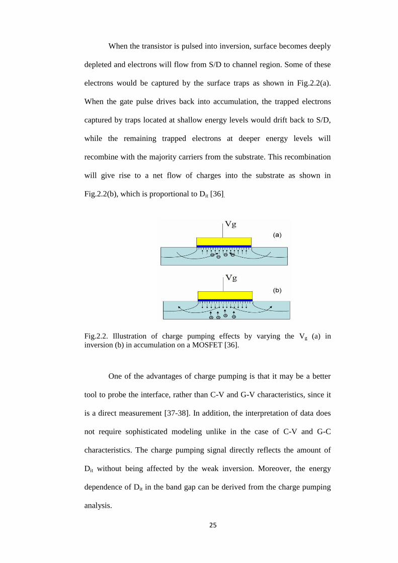
25
When the transistor is pulsed into inversion, surface becomes deeply
depleted and electrons will flow from S/D to channel region. Some of these
electrons would be captured by the surface traps as shown in Fig.2.2(a).
When the gate pulse drives back into accumulation, the trapped electrons
captured by traps located at shallow energy levels would drift back to S/D,
while the remaining trapped electrons at deeper energy levels will
recombine with the majority carriers from the substrate. This recombination
will give rise to a net flow of charges into the substrate as shown in
Fig.2.2(b), which is proportional to Dit [36].
Fig.2.2. Illustration of charge pumping effects by varying the Vg (a) in
inversion (b) in accumulation on a MOSFET [36].
One of the advantages of charge pumping is that it may be a better
tool to probe the interface, rather than C-V and G-V characteristics, since it
is a direct measurement [37-38]. In addition, the interpretation of data does
not require sophisticated modeling unlike in the case of C-V and G-C
characteristics. The charge pumping signal directly reflects the amount of
Dit without being affected by the weak inversion. Moreover, the energy
dependence of Dit in the band gap can be derived from the charge pumping
analysis.

26
One of the disadvantages of this technique is that at 300K, only a
small portion of the traps within the InxGa1-xAs bandgap is scanned and
hence resulting in underestimation of the true value of the Dit. By measuring
at lower temperature, the Dit distribution can be characterized across a wider
portion of the bandgap since the electron and hole emission levels move
closer to the band edges. Thus a monotonous increase in charge pumping
current is expected when lowering the temperature. Another way to
characterize the Dit distribution across a wider portion of the bandgap is to
measure with shorter transition times. According to emission level theory,
lowering the transition times below 100ns at 300K will enable Dit to be
scanned further into the energy band gap.
In this work, as shown in Fig.5.3 in Section 5.2.3.1, we have used
this method to evaluate the trap density across the HfAlO/In0.53Ga0.47As
plasma-PH3/N2 and non-passivated devices. However, due to lack of
equipment for measurement with varying temperature, data from charge
pumping measurement carried out only at room temperature will be studied.
Nevertheless, it is sufficient to show that interface trap density is effectively
reduced at areas near the upper half of the bandgap with plasma-PH3/N2
treatment.
2.3. Overview of Gate Leakage Mechanisms
Several mechanisms contribute to gate leakage current. Conduction
mechanisms can be grouped into electrode limited conduction mechanisms
(injection limited conduction mechanisms) or bulk limited condution
mechanisms, which depend only on the properties of the dielectric itself.
Measuring the temperature dependent conduction currents helps to
27
determine the constitution of the conduction currents. Electrode limited
conduction mechanisms include Schottky emission (SE), Fowler Nordheim
(FN) tunnelling, direct tunnelling and thermionic field emission. Bulk
limited conduction mechanisms include Frenkel Poole emission, hopping
conduction, ohmic conduction and Space Charge limited conduction. In this
section, space charge limited conduction and Frenkel Pool emission would
be explained since these mechanisms are found to exist in our non-
passivated HfAlO/In0.53Ga0.47As MOSFET which could be responsible for
its higher leakage current compared to the plasma-PH3/N2 passivated
HfAlO/In0.53Ga0.47As MOSFET.
2.3.1. Space Charge Limited Conduction
Mott and Gurney stated that under applied bias, the free carrier
concentration can be increased due to the injection of free carriers in the
vicinity of a junction formed by different materials [39]. The space charge
effect is said to occur when the injected free-carrier concentration is larger
than the thermal equilibrium value. The injected carriers influence the space
charge and the electric field profile which drives the current. The current
produced due to the presence of a space charge effect is called the Space-
Charge-Limited (SCL) current [40].
When electrons are thermally excited to energy sufficient to
overcome the barrier, Φ, at the emission surface, electrons would be injected
into the conduction band of the material, in this case gate oxide. The
frequent collisions with the phonons of the oxide and the structural
imperfections in the oxide are the dominant factors of electron flow in the
conduction band of the oxide [41]. Mott and Gurney observed that the

28
presence of localized electron traps located in the forbidden gap could
drastically interfere with the passage of injected current [42]. Rose then
gave a detailed description of the form and magnitude of the reduction in
injected current due to localized trapping of the injected carriers [39].
2.3.1.1 Trap Free Insulator and Insulator with Shallow Traps
A possible source of these electrons leading to gate leakage might be
a set of donor-like traps so shallow that they are not effective as electron
traps Here, once the injected free electron concentration becomes
comparable to the thermally generated electrons, the current voltage
characteristics will depart from Ohm’s law and follow the Trap-Free square
law. The onset of SCL current injection will place at the crossover voltage
Vx (Trap Free) defined in Fig.2.3. This current voltage characteristic is true
for trap-free insulators or when trap states do not dominate the transport. For
such insulators, the J-V characteristics within the Trap-free Square Law
regime in Fig.2.3 is described with slope given by ~2 [43].
On the other hand, insulators containing shallow traps have different
current-voltage characteristics. The current voltage curve follows Ohm’s
law and transitions to the given crossover voltage Vx (shallow traps) is
determined as Equation (2.1):
As long as the Fermi level lies below the trap level Et , the traps are shallow
and the current voltage characteristics follows the “Shallow Trap I-V
Characteristics” regime after it transitions from Ohm’s law. In this regime,
Equation (2.1)

29
the slope would be given by ~3 due to presence of trap states that are
exponentially distributed in energy [43] i.e. known as EDT-SCLC
mechanism. Following this, the Fermi level keeps rising as electrons are
being injected. Thus, at V=VTFL, the Fermi level crosses Et and the current
voltage curve merges with the Trap Filled Limited (TFL) law. After Fermi
level crosses Et, these traps become deep traps and current increases sharply
for small change in voltage at VTFL [39]. A typical current-voltage
characteristic for the case of trap free insulator and insulator with shallow
traps is shown in Fig.2.3 [44].
Fig.2.3. Space Charge limited current voltage characteristics for insulators
containing trap free and shallow traps [44].
Hence, based on the explanation above, the SCLC mechanism is
identified to be present as Trap-Free SCLC mechanism for plasma-PH3/N2
passivated device and EDT-SCLC mechanism for non-passivated device as
shown in Section 4.2.2.2. Despite the Trap-Free Square Law showing larger
gate leakage current than regime “Shallow Trap I-V Characteristics” regime
in Fig.2.3, the experimental results obtained in this work shows non-

30
passivated device giving larger gate leakage current than passivated device
in Fig.4.6 from Section 4.2.2.1. This is due to the larger ohmic conduction
current for non-passivated device compared to plasma-PH3/N2 passivated
device.
2.3.2. Frenkel Poole (FP) Emission
FP emission results from the lowering of Coulombic potential barrier
by an applied electric field. The FP effect is associated with barrier at the
trap well in the bulk of the insulator film i.e. the coulomb potential energy
of the electrons in a trapping center can be reduced by an applied field
across the dielectric film shown in Fig.2.4. Hence, this reduction in potential
energy can increase the probability of an electron being thermally excited
out of the trap into the conduction band of the dielectric. The leakage
current associated with FP emission can be determined by utilizing the
following Equation (2.2).
where Nc is the density of states in the conduction band, µ is the mobility,
qt is the trap energy level, E is the electric field and r is the dynamic
dielectric constant. For FP emission the plot of ln(J/E) vs E1/2
should be
linear with the inverse of the slope corresponding to reported r of the high-k
oxide [45]. Since FP emission is owing to the thermal activation under an
electric field, this conduction mechansim is often observed at high
temperature and high electric field. This mechanism is identified in the high
field region of non-passivated device given in Section 4.2.2.2 in Fig.4.9.
Equation (2.2)

31
Fig.2.4. Schematic energy band diagram of Frenkel Poole emission [45].
2.4. Overview of Mobility Scattering Mechanisms on high-
k/InxGa1-xAs MOS Devices
So far, several scattering mechanisms on high-k/InxGa1-xAs devices
have been observed, and they include mechanisms such as interface
roughness [46], interface dipole scattering [47] and remote Coulombic
scattering due to charges in the oxide and/or at the interface as well as
phonon scattering [48]. These scattering mechanisms would be shown in
this section.
2.4.1. Coulombic Scattering and Phonon Scattering
At low Eeff, Coulombic scattering dominates and the mobility
increases with higher inversion carrier density due to the screening effect.
This is observed in LaAlO3/InxGa1-xAs MOSFET [48]. The Coulombic
scattering at low inversion charge could be attributed to the net positively
charged donor states present at the interface between the InxGa1-xAs channel
and the high-k/LaAlO3 dielectric. The phonon limited mobility, μPhonon,
dominates across a wide range of carrier density as indicated by the strong
temperature dependence, in particular those caused by substrate/bulk
phonons. It is proposed that the phonons could originate remotely from the

32
high-k dielectric or could be associated with the polar nature of the
InxGa1-xAs semiconductor or an interaction between the two [48-49].
Hence, mobility data in Chapter 5 of this work given in Sections
5.2.2 and 5.2.3 will be analysed in the light of this discussion to identify
dominant scattering mechanism and suppression of certain mechanisms due
to passivation.
2.4.2. Interface Dipole Scattering
One of the reasons proposed for the improved mobility of ALD
Al2O3 on InxGa1-xAs (111) A MOSFET compared to InxGa1-xAs (100) A
MOSFET is interface dipole scattering based on the fact that μeff
improvements under high Eeff is associated with Vth shift to the negative
direction [47]. The cause of this Vth shift is due to the interface dipoles at
Al2O3/InxGa1-xAs as deduced from the y intercept of Vfb vs EOT which
indicates a large interface dipole strength for InxGa1-xAs (111) A compared
to InxGa1-xAs (100) A.
Hence in our work, we have made use of similar technique to
identify the presence of larger interface dipole scattering for non-passivated
device compared to passivated device as shown in Fig.5.9 from Section
5.2.3.3.

33
2.5. Process Flow of In0.53Ga0.47As MOSFETs Fabricated
Fig.2.5. MBE growth of p-In0.53Ga0.47As on InP with the specifications
provided. In0.53Ga0.47As is 500nm thick, lattice matched with InP.
The process flow for device fabrication has been performed on the
heterostructure substrate, which has been provided from commercial growth
services, given in Fig.2.5. MBE method was used to grow the 2-inch p+ InP
substrate (doping level is 3x10¹⁸
cm-3
), 200nm p-doped (doping level is
1x10¹⁸
cm-3
) InP buffer and 500nm p-doped In0.53Ga0.47As. The dopants used
for p-type formation is Zn and doping level has been extracted from the
electrochemical capacitance-voltage (ECV) method.
Similar to the fabrication of silicon MOS device, the surface
preparation is an important step before growth or deposition of dielectric.
The In0.53Ga0.47As surface was first cleaned using 1% dilute HF for 2min to
remove the native oxide originating from the surface. HF cleaning for 2min
does not significantly attack the surface resulting in surface roughness to
only increase slightly, measured from the Atomic Force Microscopy (AFM).
Since surface passivation by Chalcogen atoms such as sulphur and selenium
has been widely adopted in In0.53Ga0.47As devices for surface passivation,
InP substrate (Zn p+)
InP buffer (Zn p+)
In0.53Ga0.47As (500nm, Zn doped)
34
(NH4)2S cleaning has been carried out for 5min at room temperature to
prevent oxidation caused by exposure to the ambient. This is followed by
3min de-ionized water rinse, as the standard pre-gate cleaning procedure.
Subsequently, the p-type In0.53Ga0.47As devices needed for plasma-
PH3/N2 passivation were loaded into the holder of the multichamber
chemical vapor deposition system with substrate temperature being
maintained at 430°C and they were treated with plasma-PH3/N2 treatment
for 1min. Thus devices which undergo plasma-PH3/N2 passivation treatment
is termed as passivated device while devices which do not undergo plasma-
PH3/N2 passivation treatment is termed as non-passivated device. Without
breaking vacuum, both passivated and non-passivated devices then
immediately underwent metalorganic CVD (MOCVD) of HfAlO using
[HfAl(MMP)2(OiPr)5] as precursor, at 450°C and post-deposition anneal at
400°C for 30s in N2 ambient. It is comprised of 10% Al2O3 and 90% HfO2.
The advantage of HfAlO over HfO2 is that the crystallization temperature is
higher for HfAlO, causing it to have better thermal stability than HfO2 and
also easier removal by HF to form the S/D contact opening after a high
temperature process. Chapter 3 studies involves 8nm thick high-k HfAlO,
while Chapter 4-Chapter 5 involves 5nm thick HfAlO. For long channel
devices fabricated from both runs, the channel doping concentration of p-
type In0.53Ga0.47As is 1x10¹⁶
cm-3
.
2.5.1. Long Channel MOSFET Fabrication Process
After gate oxide deposition process, device fabrication for the
MOSFETs followed the conventional self-aligned process where a 150nm

35
TaN film was first deposited by sputtering Ta using Ar/N2 gas as a gate
electrode. Next, gate area was defined by Cl2 based reactive ion etching.
Silicon is then implanted through 10nm of sacrificial SiO2, deposited
using e-beam evaporator, into the In0.53Ga0.47As with dose of 1x10¹⁴
cm-2
and
energy of 50keV. This is then followed by a 100nm SiO2 capping layer
deposition before sample undergoes various activation conditions, in this
case 600°C 1min in N2 ambient. The RTA system uses a standard setup for
8-inch silicon wafer, and the In0.53Ga0.47As sample is placed on top of a
dummy 8-inch silicon wafer where temperature is then monitored by a
Pyrometer. After RTA, SiO2 capping layer is then removed. The implant
and annealing condition are chosen since good rectifying junction with
forward and reverse current ratio as 6 orders of magnitude can be achieved,
with low sheet resistance of the Si implanted region being 65-80Ω/sq and
contact resistance determined to be about 600Ω.µm [1].
The ohmic S/D contacts were then made by photolithography and
electron beam evaporation of AuGe 50nm/Ni 25nm /Au 50nm alloy. This is
then followed by lift off process, using acetone/ultrasonic bath and
subsequently IPA and DI rinse. Metal alloying RTA was carried out at
360°C-400°C for 1min in N2. As a back contact, Ti/Pt/Au alloying was
used. Final step involved forming gas anneal (FGA) performed at 10%
H2/90% N2 concentration at 400°C for 10min. Hence, the process flow for
fabrication of In0.53Ga0.47As MOSFET is shown in Fig.2.6.

36
MBE grown In0.53Ga0.47As
HF and (NH4)2S surface treatment
Plasma-PH3/N2 treatment (optional)
HfAlO deposition
In-situ PDA 400°C 30s
Sputter TaN deposition
Gate etch and high-k etching
Si implantation (50keV/1x1014
cm-2
)
S/D activation RTA 600°C 60s
S/D and back contact formation
Forming Gas Anneal (FGA) 10% H2/90% N2 concentration at 400°C for 10min
Fig.2.6. Process flow of long channel In0.53Ga0.47As N-MOSFET fabrication.
Note that the processes described is for the fabrication of long
channel MOSFETs (≥ 2µm devices) fabricated in the form of a ring-shape
gate In0.53Ga0.47As MOSFET as shown in Fig.2.7.
Fig.2.7. Top view of a ring shape In0.53Ga0.47As MOSFET, fabricated using a
two-mask step.
This is known as a two-mask transistor process since one mask is for
ring-shape gate pattern and device isolation. Another mask is for the source
and drain contact pattern. Typical gate lengths fabricated using this process
is 2µm-20µm with the width being 200µm-400µm an additional square area
of 100x100µm2
for probing. Fig.2.8 is the schematic of the MOSFET
formed using above process and is used for Chapter 3-5 long channel
MOSFET studies. However, devices fabricated in Chapter 4-5 does not
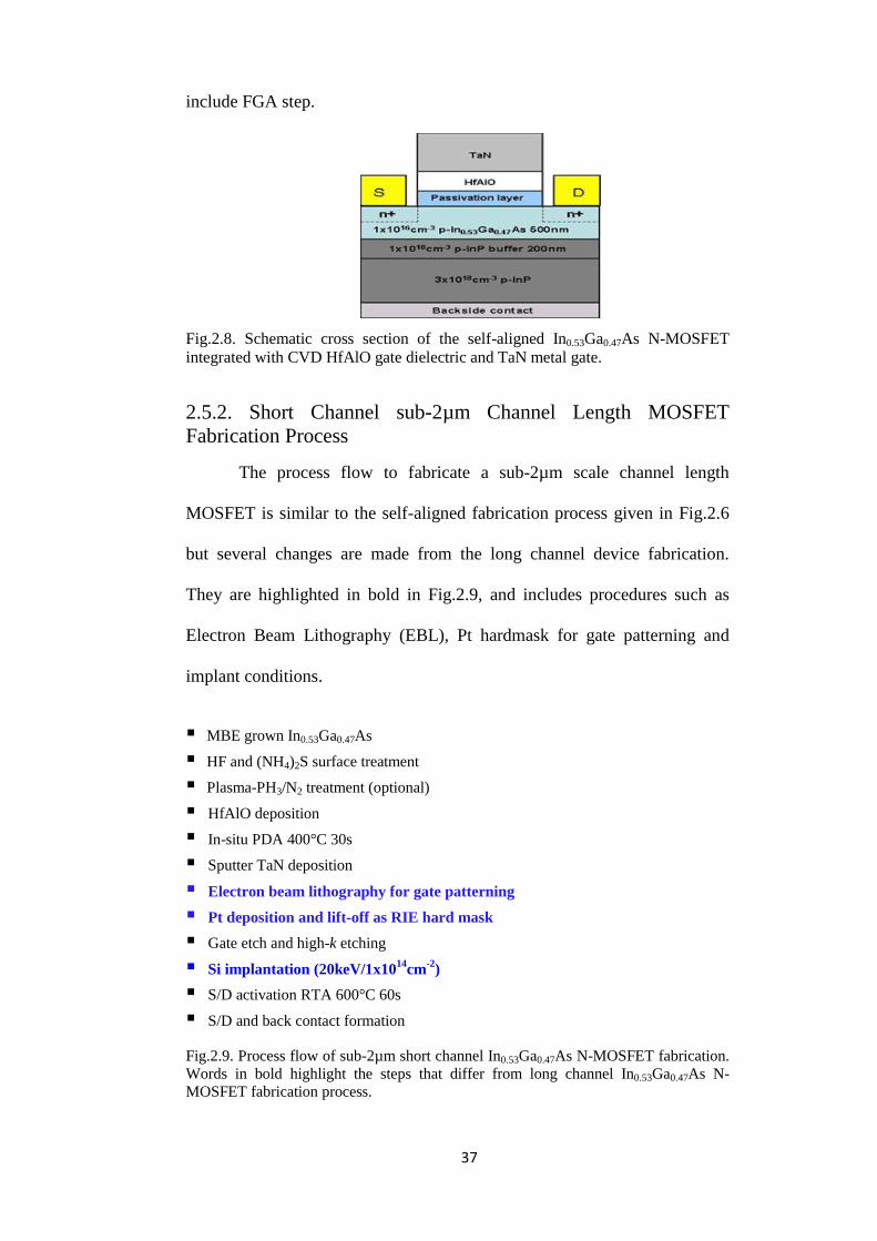
37
include FGA step.
Fig.2.8. Schematic cross section of the self-aligned In0.53Ga0.47As N-MOSFET
integrated with CVD HfAlO gate dielectric and TaN metal gate.
2.5.2. Short Channel sub-2µm Channel Length MOSFET
Fabrication Process
The process flow to fabricate a sub-2µm scale channel length
MOSFET is similar to the self-aligned fabrication process given in Fig.2.6
but several changes are made from the long channel device fabrication.
They are highlighted in bold in Fig.2.9, and includes procedures such as
Electron Beam Lithography (EBL), Pt hardmask for gate patterning and
implant conditions.
MBE grown In0.53Ga0.47As
HF and (NH4)2S surface treatment
Plasma-PH3/N2 treatment (optional)
HfAlO deposition
In-situ PDA 400°C 30s
Sputter TaN deposition
Electron beam lithography for gate patterning
Pt deposition and lift-off as RIE hard mask
Gate etch and high-k etching
Si implantation (20keV/1x1014
cm-2
)
S/D activation RTA 600°C 60s
S/D and back contact formation
Fig.2.9. Process flow of sub-2µm short channel In0.53Ga0.47As N-MOSFET fabrication.
Words in bold highlight the steps that differ from long channel In0.53Ga0.47As N-
MOSFET fabrication process.

38
Sub-2µm HfAlO In0.53Ga0.47As NMOSFET has been fabrication with
plasma-PH3/N2 treatment. Pt is used since it is resistive to RIE etching. After
drawing the gate using electron beam lithography, Pt is deposited followed
by Pt lift-off. This is then followed by positive resist being spin coated onto
the wafer before optical lithography step consisting of exposure and
development is carried out. Next involves the RIE and ashing process for
photoresist removal. Hence, now only gate line region consists of Pt
remaining on top of TaN. The SD contact is then formed after implantation
and RTA activation using a second masking layer for pattern formation and
lift off. Note that the process flow described in this section is used for the
device fabrication of sub-2µm devices in Chapter 3 (Section 3.3-3.4), as
well as device taken from our group’s IEDM 2008 data which is used for
TCAD calibration parameters from Chapter 6. In addition, the p-type doping
concentration for In0.53Ga0.47As channel fabricated for the short channel
devices in this work in Chapter 3 is given by 1x10¹⁶
cm-3
.

39
REFERENCES
[1]J.Q. Lin, S.J. Lee, H.J. Oh, G.Q. Lo, D.L. Kwong, and D.Z. Chi, “Inversion
mode self-aligned In0.53Ga0.47As n-channel metal-oxide-semiconductor field-effect
Characterization and Passivation of III-V/High-k Interfaces transistor with HfAlO
gate dielectric and TaN metal gate”, IEEE Elec.Dev. Lett., Vol. 29, pp. 977-980,
2008.
[2]H.C. Lin, W. -E. Wang, G. Brammertz, M. Meuris, and M. Heyns, “Electrical
study of sulfur passivated In0.53Ga0.47As MOS capacitor and transistor with ALD
Al2O3 as gate insulator”, Microelectronic Eng., Vol. 86, pp. 1554-1557, 2009.
[3]Y. Xuan, Y.Q. Wu, T. Shen, T. Yang, and P.D. Ye, “High performance
submicron inversion-type enhancement-mode InGaAs MOSFETs with ALD Al2O3,
HfO2 and HfAlO as gate dielectrics”, Tech. Dig. – Int. Electron Devices Meet, pp.
637-640, 2007.
[4]M.V. Lebedev, T. Mayer, and W. Jaegermann “Sulfur adsorption at GaAs (100)
from solution: role of the solvent in surface chemistry”, Surf. Sci.,Vol. 547, pp.
171- 183, 2003.
[5]T.Scimeca,Y.Muramatsu,M.Oshima,H.Oigawa, and Y. Nannichi, “Temperature-
dependent changes on the sulfur-passivated GaAs (111)A, (100), and (111)B
surfaces”, Phys. Rev. B., Vol. 44, pp. 12927-12932, 1991.
[6]I. Ok, H.-S. Kim, M. Zhang, C.Y. Kang, S.J. Rhee, C. Choi, S.A. Krishnan, T.
Lee, F. Zhu, G. Thareja, and J.C. Lee, “Metal gate- HfO2 MOS structures on GaAs
substrate with and without Si interlayer”, IEEE Elec.Dev. Lett, Vol.27, pp.145,
2006.
[7]S.J. Koester, E.W. Kiewra, Y. Sun, D.A. Neumayer, J.A. Ott, M. Copel, D.K.
Sadana, D. J. Webb, J. Fompeyrine, J.-P. Locquet, C. Marchiori, M. Sousa, and R.
Germann, “Evidence of electron and hole inversion in GaAs metal-oxide-
semiconductor capacitors with HfO2 gate dielectrics and α-Si/SiO2 interlayers”,
App. Phy. Lett., Vol.89, pp.042104, 2006.
[8]M. Sonnet, C.L. Hinkle, M.N. Jivani, R.A. Chapman, G.P. Pollack, R.M.
Wallace, and E.M. Vogel, “Performance enhancement of n-channel inversion type
InGaAs metal oxide semiconductor field effect transistor using ex-situ deposited
thin film amorphous silicon layer”, Appl.Phys.Lett., Vol.93, pp.122109, 2008.
[9]C.L. Hinkle, A.M. Sonnet, R.A. Chapman, and E.M. Vogel, “Extraction of the
Effective mobility of In0.53Ga0.47As”, IEEE Elec.Dev.Lett., Vol.30, pp.316, 2009.
[10]M.J. Hale, S.I. Yi, J.Z. Sexton, A.C. Kummel, and M. Passlack, “Scanning
tunneling microscopy and spectroscopy of gallium oxide deposition and oxidation
on GaAs(001)-c(2×8)/(2×4)”, J. Chem. Phys., Vol.119, pp.6719, 2003.
[11]R. Kambhampati, S. Koveshnikov, V. Tokranov, M. Yakimov, R. Moore, W.
Tsai, and S. Oktyabrsky, “In-Situ Deposition of high-k Gate Stack on InGaAs and
GaAs for Metal-Oxide- Semiconductor Devices with Low Equivalent Oxide
Thickness”, ECS Transactions, Vol.11, pp.431–439, 2007.
[12]S. Koveshnikov, N. Goel, P. Majhi, H. Wen, M. B. Santos, S. Oktyabrsky,
V.Tokranov, R. Kambhampati, R. Moore, F. Zhu, J. Lee, and W. Tsai,

40
“In0.53Ga0.47As based metal oxide semiconductor capacitors with atomic layer
deposition ZrO2 gate oxide demonstrating low gate leakage current and equivalent
oxide thickness less than 1 nm”, Appl. Phys. Lett., Vol. 92, pp.222904, 2008 .
[13]R. Engel-Herbert, Y. Hwang, J. Cagnon, and S. Stemmer, “Metal-oxide-
semiconductor capacitors with ZrO2 dielectrics grown on In0.53Ga0.47As by
chemical beam deposition”, Appl. Phys.Lett., Vol.95, pp.062908, 2009.
[14]H.-C. Lin,W.-E. Wang, G. Brammertz, M. Meuris, and M. Heyns, “Electrical
study of sulfur passivated In0.53Ga0.47As MOS capacitor and transistor with ALD
Al2O3 as gate insulator”, Microelectron.Eng., Vol.86, pp.1554, 2009.
[15]B. Shin, J. Cagnon, R.D. Long, P.K. Hurley, S. Stemmer, and P.C.McIntyre,
“Unpinned Interface Between Al2O3 Gate Dielectric Layer Grown by Atomic
Layer Deposition and Chemically Treated n-In0.53Ga0.47As (001) Dielectric Science
and Materials”, Electrochem. Solid-State Lett., Vol.12, pp.G40, 2009.
[16]E. O‘Connor, S. Monaghan, R.D. Long, A. O‘Mahony, I.M. Povey, K.
Cherkaoui, M. E. Pemble, G. Brammertz, M. Heyns, S.B. Newcomb, V.V.
Afanas‘ev, and P.K. Hurley, “Temperature and frequency dependent electrical
characterization of HfO2/InxGa1−xAs interfaces using capacitance-voltage and
conductance methods”, Appl. Phys. Lett., Vol.94, pp.102902, 2009.
[17]E. O‘Connor, R.D. Long, K. Cherkaoui, K.K. Thomas, F. Chalvet, I.M. Povey,
M.E. Pemble, P.K. Hurley, B. Brennan, G. Hughes, and S.B. Newcomb, “In situ
H2S passivation of In0.53Ga0.47As /InP metal-oxide-semiconductor capacitors with
atomic-layer deposited HfO2 gate dielectric”, Appl. Phys. Lett.,Vol.92, pp.022902,
2008.
[18]Y.C. Chang, M.L. Huang, K.Y. Lee, Y.J. Lee, T.D. Lin, M. Hong, J. Kwo, T.S.
Lay, C. C. Liao, and K.Y. Cheng, “Atomic-layer-deposited HfO2 on In0.53Ga0.47As:
Passivation and energy-band parameters”, Appl. Phys. Lett., Vol.92, pp.072901,
2008.
[19]R.D. Long, E. O‘Connor, S.B. Newcomb, S. Monaghan, K. Cherkaoui, P.
Casey, G. Hughes, K.K. Thomas, F. Chalvet, I.M. Povey, M.E. Pemble, and P.K.
Hurley, “Structural analysis, elemental profiling, and electrical characterization of
HfO2 thin films deposited on In0.53Ga0.47As surfaces by atomic layer deposition”, J.
Appl. Phys.,Vol.106, pp. 084508, 2009.
[20]N. Goel, P. Majhi, W. Tsai, M. Warusawithana, D. G. Schlom, M. B.Santos, J.
S. Harris, and Y. Nishi, “High-indium-content InGaAs metal-oxide-semiconductor
capacitor with amorphous LaAlO3 gate dielectric”, Appl. Phys. Lett., Vol.91,
pp.093509, 2007.
[21]H.D. Trinh, E.Y. Chang, P.W. Wu, Y.Y. Wong, C.T. Chang, Y.F. Hsieh, C.C.
Yu, H.Q. Nguyen, Y.C. Lin, K.L. Lin, and M.K. Hudait “The influences of surface
treatment and gas annealing conditions on the inversion behaviors of the atomic-
layer-deposition Al2O3/n-In0.53Ga0.47As metal-oxide-semiconductor capacitor”,
Appl.Phys.Lett.,Vol.97, pp.042903, 2010.
[22]H. Zhao, Y. Chen, J. Yum, Y. Wang, and J.C. Lee, “HfO2-based In0.53Ga0.47As
MOSFETs (EOT~10Å) using various interfacial dielectric layers”, IEEE
Dev.Res.Conf., pp.89, 2009.

41
[23]A. Jaouad and V. Aimez, “Passivation of air-exposed AlGaAs using low
frequency plasma-enhanced chemical vapour deposition of silicon nitride”, App.
Phys. Lett.., Vol.89, pp.092125-1-3, 2001.
[24]G. Brammertz, H.C. Lin, K. Martens, A. Alian, C. Merckling, J. Penaud, D.
Kohen, W.-E Wang, S. Sioncke, A. Delabie, M. Meuris, M. Caymax, and M.
Heyns, “Electrical properties of III-V/oxide interfaces”, Electrical Chemical
Society spring meetings, Vol.19, pp.375–383, 2009.
[25]D. Lin, W.-E Wang, G. Brammertz, M. Meuris, and M. Heyns, “Inversion
behavior on n and p type ALD— Al2O3/ In0.53Ga0.47As MOS capacitors”, IEEE
Semiconductor Interface Specialists Conference, 2008.
[26]H.-C. Lin, G. Brammertz , K. Martens, G. de Valicourt, L. Negre, W.-E Wang,
W. Tsai, M. Meuris, and M. Heyns, “Application of Fermi Level Efficiency
Method to the analysis of high interface trap density oxide-semiconductor
interfaces”, App.Phys.Lett.,Vol.94, pp.153508, 2009.
[27]Y.Ran Luo, “Bond dissociation energies”
[28]B.Shin, R.J.Weber, D.R.Long and K.P.Hurley, “Origin and passivation of fixed charge in atomic layer deposited aluminum oxide gate insulators on chemically treated In0.53Ga0.47As substrates”, Appl. Phys.Lett., Vol.96, pp.152908, 2010.
[29]H.D.Trinh, E.Y.Chang, P.W.Wu, Y.Y.Wong, C.T.Chang, Y.F.Hsieh, C.C.Yu,
H.Q.Nguyen, Y.C.Lin, K.L.Lin and M.K.Hudait, “The influences of surface
treatment and gas annealing conditions on the inversion behaviors of the atomic-
layer-deposition Al2O3/n-In0.53Ga0.47As metal-oxide-semiconductor capacitor”,
Appl.Phys.Lett., Vol.97, pp.042903, 2010.
[30]J.Hu and H.S. Philip, “Effect of annealing ambient and temperature on the
electrical characteristics of atomic layer deposition Al2O3/In0.53Ga0.47As metal-oxide-
semiconductor capacitors and MOSFETs “, J.Appl.Phys, Vol.111, pp. 044105, 2012.
[31]T. Hoshii, M. Yokoyama, H. Yamada, M. Hata, T. Yasuda, M. Takenaka, and S.
Takagi, “Impact of InGaAs surface nitridation on interface properties of InGaAs
metal-oxide semiconductor capacitors using electron cyclotron resonance plasma
sputtering SiO2”, Appl.Phys.Lett, 97,132102, 2010.
[32]S.Pal, S.M.Shivaprasad, Y.Aparna and B.R.Chakraborty,“Phosphorous
passivation of In0.53Ga0.47As using MOVPE and characterization of Au–Ga2O3
(Gd2O3)–In0.53Ga0.47As MIS capacitor”, Appl.Surf.Sci., Vol.245, pp.196-201, 2005.
[33]Oh Hoon Jung, “Development of High Mobility Channel Layer Formation
Technology for High Speed CMOS Devices”, PhD Dissertation, National
University of Singapore, 2010.
[34]J.S. Brugler and P.G.A. Jespers, "Charge pumping in MOS devices", IEEE
Trans. Elec.Dev., Vol.16, pp. 297-302, 1969.
[35]G. Groeseneken, H.E. Maes, N. Beltran, and R.F. Dekeersmaecker, "A Reliable
Approach to Charge-pumping Measurements in MOS-Transistors", IEEE Trans.
Elec.Dev., Vol. 31, pp. 42-53, 1984.
[36]XieRuilong,“Development and Characterization of high-k Dielectric/Germanium
Gate Stack”, Ph.D Dissertation, National University of Singapore, 2009.
[37]E.H. Nicollain, MOS physics and Technology, Wiley 2003.

42
[38]K. Martens, C.O. Chui, G. Brammertz, B. De Jaeger, D. Kuzum, M. Meuris, M.
Heyns, T. Krishnamohan, K. Saraswat, H.E. Maes, G. Groeseneken, “On the
correct extraction of interface trap density of MOS devices with high-mobility
semiconductor substrates”, IEEE Trans. Elec. Dev.,Vol.55, pp. 547-555, 2008.
[39]A. Rose “Space Charge limited currents in solids”, Physical Review, Vol.97,
No.6, p.1538-1544, March 1955.
[40]K.K. Ng, “Complete Guide To Semiconductor Devices”, 2nd
Edition, John
Wiley & Sons, New York, 2002.
[41]M.A. Lampert and P. Mark, “Current Injection in Solids”, Academic Press,
New York, 1970.
[42]N. F. Mott, R. W. Gurney, “Electronic Processes in Ionic Crystals”, Oxford
University Press, London and New York, 1940.
[43]D. Joung, A. Chuner, L. Zhai and S.I. Khondaker, “Space charge limited
conduction with exponential trap distribution in reduced graphene oxide sheets”,
Appl.Phys.Lett.,Vol.97, pp.093105, 2010.
[44]Satoshi Takeshita, “Modelling of space charge limited current injection
incorporating an advanced model of the Poole Frenkel effect”, Master of
Science Thesis, Graduate School of Clemson University, 2008.
[45]G. He and Z. Sun, “High-k Gate Dielectrics for CMOS Technology”,
Wiley 2012, from Book Chapter, “Structural and Electrical Characteristics of
Alternative High-k Dielectrics for CMOS Applications”.
[46]W. Wang, J.C. M. Hwang, Y. Xuan, and P.D. Ye, “Analysis of Electron
Mobility in Inversion-Mode Al2O3/InxGa1−xAs MOSFETs”,IEEE
Trans.Ele.Dev.,Vol.58, pp.1972, 2011.
[47]Y. Urabe, N. Miyata, H. Ishii, T. Itatani, T. Maeda, T. Yasuda, H. Yamada,
N. Fukuhara, M. Hata, M.Y okoyama, N. Taoka, M. Takenaka, S. Takagi,
“Correlation between Channel Mobility Improvements and Negative Vth Shifts
in III-V MISFETs: Dipole Fluctuation as New Scattering Mechanism”, Tech.
Dig. – Int. Electron Devices Meet., pp. 142-145, 2010.
[48]A. Ali, H. Madan, S. Koveshnikov and S. Datta, “Small Signal Response of
Inversion Layers in High Mobility In0.53Ga0.47As MOSFETs Made with Thin
high-k Dielectrics”, IEEE Trans. Elec.Dev., Vol. 57, pp. 742-748, 2010.
[49]B. Benbakhti, K. Kalna and A. Asenov, “Device simulations of III-V and
Ge MOSFETs”, DUALLOGIC, Jun. 2009.
43
Chapter 3: Thermal stability and Electrical Performance
of plasma-PH3/N2 Passivated HfAlO/In0.53Ga0.47As
MOSFET
3.1. Introduction and Motivation
Plasma-PH3/N2 passivation treatment has been previously shown to
result in better HfO2/In0.53Ga0.47As interfacial properties as well as device
transfer characteristics compared to the device without the passivation [1-2].
It is shown from XPS and AFM, based on our previous studies [2-3], that a
low pressure plasma-PH3/N2 treatment of In0.53Ga0.47As results in a smooth
and atomically thin PxNy film as the main product, with P-for-As anion
exchange layer found beneath the PxNy layer in a wide range of process
window. This P-for-As exchanged layer together with the PxNy layer
formation is responsible for the prevention of the evolution of undesired As
species such as free As.
However, these studies lack in thermodynamic evaluation. This
chapter thus focuses on thermodynamic stability study of the In0.53Ga0.47As
MOSFET, which is essential for devices fabricated using gate-first technique.
The key issue in demonstrating self-aligned In0.53Ga0.47As MOSFETs is to
maintain the electrical quality of the high-k/In0.53Ga0.47As interface while
achieving high dopant activation in the S/D. Hence, the thermal stability of
the In0.53Ga0.47As MOSFETs passivated with plasma-PH3/N2 treatment is
studied by examining the properties of the high-k/In0.53Ga0.47As interface
using transmission electron microscopy (TEM), energy dispersion X-ray
(EDX), capacitance–voltage (C-V), and charge pumping techniques. It will be
shown that plasma-PH3/N2 passivation treatment has excellent thermal
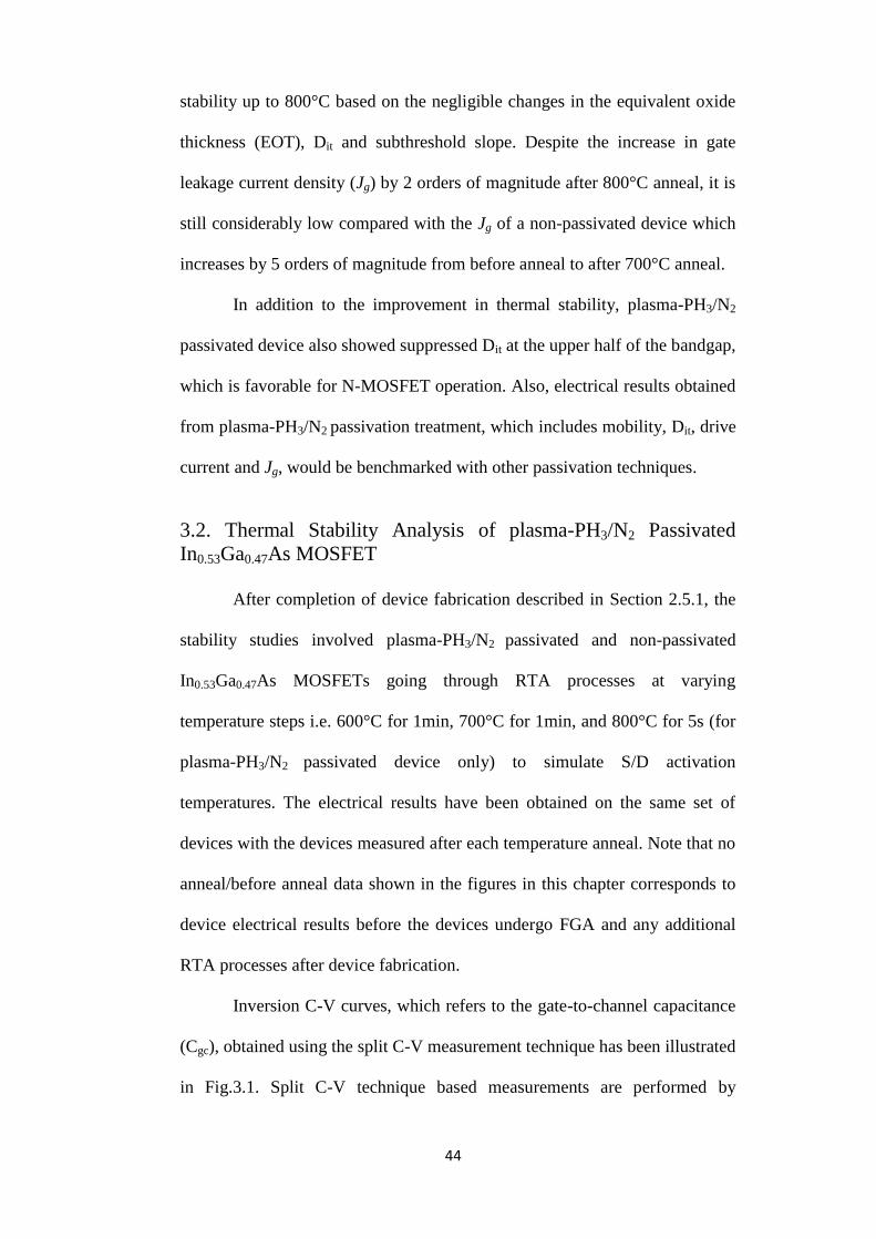
44
stability up to 800°C based on the negligible changes in the equivalent oxide
thickness (EOT), Dit and subthreshold slope. Despite the increase in gate
leakage current density (Jg) by 2 orders of magnitude after 800°C anneal, it is
still considerably low compared with the Jg of a non-passivated device which
increases by 5 orders of magnitude from before anneal to after 700°C anneal.
In addition to the improvement in thermal stability, plasma-PH3/N2
passivated device also showed suppressed Dit at the upper half of the bandgap,
which is favorable for N-MOSFET operation. Also, electrical results obtained
from plasma-PH3/N2 passivation treatment, which includes mobility, Dit, drive
current and Jg, would be benchmarked with other passivation techniques.
3.2. Thermal Stability Analysis of plasma-PH3/N2 Passivated
In0.53Ga0.47As MOSFET
After completion of device fabrication described in Section 2.5.1, the
stability studies involved plasma-PH3/N2 passivated and non-passivated
In0.53Ga0.47As MOSFETs going through RTA processes at varying
temperature steps i.e. 600°C for 1min, 700°C for 1min, and 800°C for 5s (for
plasma-PH3/N2 passivated device only) to simulate S/D activation
temperatures. The electrical results have been obtained on the same set of
devices with the devices measured after each temperature anneal. Note that no
anneal/before anneal data shown in the figures in this chapter corresponds to
device electrical results before the devices undergo FGA and any additional
RTA processes after device fabrication.
Inversion C-V curves, which refers to the gate-to-channel capacitance
(Cgc), obtained using the split C-V measurement technique has been illustrated
in Fig.3.1. Split C-V technique based measurements are performed by

45
grounding the substrate and measuring the capacitance between gate and S/D
connected together. The curves measured at 100kHz show sharp transitions
from accumulation to inversion after annealing the plasma-PH3/N2 passivated
MOSFETs until 800°C in Fig.3.1. As seen in the figure, no presence of kinks
and C-V stretch out at 800°C anneal can be observed. The EOT shows
negligible changes up to 800°C anneal, with EOT~2.7nm before anneal and
EOT~2.8nm after 800°C anneal. This shows the robustness of the PxNy gate
stack and the gate stack/In0.53Ga0.47As heterostructures after RTA, which can
be attributed both to the superior thermal [4-7] and chemical stability [2,4,8]
of the PxNy barrier layer against oxidation caused by the strong P–N bond that
can suppress the formation of a defective low-k interfacial layer. The thermal
stability of PxNy is helpful here since its decomposition temperature is higher
than 850°C [5-6, 9].
The Jg extracted after each annealing step which are plotted in the
inset of Fig.3.1, shows that at 600°C N2 anneal, there are no significant
changes in Jg compared to the result before anneal. However, the leakage
current in these devices increased by 2 orders of magnitude after 800°C 5s
anneal i.e. from 2x10⁻⁷
A/cm2 for no anneal to 1.95x10
−5A/cm
2 at Vg=1V.
Nevertheless, this Jg of ~1.95x10⁻⁵
A/cm2, is still considerably low compared
with the Jg of a non-passivated device, which significantly increases by 5
orders of magnitude from 9.44x10⁻⁷
A/cm2 for no anneal to 5.16x10
−1A/cm
2 at
Vg=1V after 700°C 1min anneal. This low electrical gate leakage
demonstrates that the HfAlO/PxNy gate stack has good thermodynamic
stability and integrity even after high temperature anneal.

46
Fig.3.1. Cgc curves, generated from split C-V measurement technique, measured
at 100kHz of plasma-PH3/N2 passivated devices as a function of temperatures at
600°C N2 1min, 700°C N2 1min and 800°C N2 5s. Note the 2 order increase in Jg
after high temperature anneal.
Fig.3.2(a) to Fig.3.2(d) shows the TEM images of the
HfAlO/PxNy/In0.53Ga0.47As gate stack used in above measurements. Alloying
the HfO2 film with Al2O3, it is known that the crystallization temperature of
HfO2 film will be increased [10] as seen in Figs.3.2(a)-(d) where the HfAlO
remains amorphous up to 800°C anneal. It can be observed that the interface
between In0.53Ga0.47As and the passivation layer is smooth until 600°C anneal.
However, the sharp transition from the crystalline In0.53Ga0.47As substrate to
the PxNy layer can no longer be observed at 800°C in Fig.3.2(c) due to the
structural changes seen at the localized rough In0.53Ga0.47As interface caused

47
by the poor thermal stability of In0.53Ga0.47As that starts to show Ga/As out-
diffusion at 800°C [11]. The localized rough interface in Fig.3.2(c) and the
EDX data (as shown in Fig.3.3(a)) could suggest the migration of Ga/As
upward [12]. The interface roughness is found only in localized regions and
not seen throughout, as shown in Fig.3.3(b) where the EDX data show no
Ga/As outdiffusion. This results in a uniform HfAlO/In0.53Ga0.47As interface
seen from the TEM image in Fig.3.2(d)). However, the relatively unchanged
C-V curves in Fig.3.1, the consistent Dit in Fig.3.4, relatively consistent
transconductance in the linear region in Fig.3.5 and consistent subthreshold
slope in Fig.3.6 suggest that such roughness is confined to a small region of
total width. Nevertheless, the localized interface roughness observed suggests
the need to find the optimum condition for the PH3/N2 passivation process.
The localized thinning of HfAlO and the outdiffusion of Ga/As could be
responsible for the increase in Jg for the plasma-PH3/N2 passivated
In0.53Ga0.47As device due to strong exponential dependence on oxide weak
spots. The frequency dispersion (C10kHz-1MHz/C10kHz) and hysteresis (difference
in flatband voltage for 100kHz C-V curves obtained from forward and reverse
sweeps) in inversion C-V of the plasma-PH3/N2 passivated devices are not
significantly altered. They are ranging between 2.3% and 2.9% and 48mV and
52mV for frequency dispersion and hysteresis, respectively, with varying
annealing temperature before anneal to 800°C.

48
TaN TaN
HfAlO HfAlO
InGaAs InGaAs
(a) (b)
TaN
HfAlO
InGaAs
(c)
Fig.3.2. TEM images of HfAlO/plasma-PH3/N2 passivated In0.53Ga0.47As gate
stack with (a) no activation anneal but with FGA 400°C (b) 600°C 1min
activation anneal with FGA 400°C and (c) 600°C 1min activation anneal with
FGA 400°C followed by 800°C anneal 5s. (d) Same annealing condition as (c)
but showing the good even HfAlO layer on even In0.53Ga0.47As surface. Note that
oxide thickness measured from TEM is given by ~8nm.

49
The Dit at the upper and lower halves of the bandgap of the
In0.53Ga0.47As N-MOSFETs is measured using the variable rise/fall time of the
charge pumping technique [13-14], with constant amplitude gate pulse at a
frequency of 100kHz and gate pulse amplitude of 1.2V. The fall time (rise
Fig.3.3. EDX results of HfAlO/PxNy/In0.53Ga0.47As gate stack with 600°C
activation anneal FGA 400°C followed by 800°C anneal at (a) localized rough
interface taken from Fig.3.2(c) of TEM image and (b) uniform smooth interface
taken from Fig.3.2(d) of TEM image.

50
time) is varied between 100ns and 1000ns while keeping the rise time (fall
time) constant at 100ns to find the electron emission energy level above the
midgap (hole emission energy level below the midgap) of the bandgap. In
Fig.3.4, the Dit above the midgap is smaller than below midgap for plasma-
PH3/N2 passivated device. This means that either donor-like traps or acceptor-
like traps or both in the upper half of the bandgap for passivated device exist
in lesser concentration than in lower half of bandgap. Since subthreshold
slope alone cannot distinguish between acceptor/donor-like traps, the lower
on-current (Ion) and lower transconductance can be used to deduce that there is
greater acceptor-like traps for non-passivated compared to plasma-PH3/N2
passivated N-MOSFET as seen in Fig.3.5. Greater concentration of acceptor-
like traps causes larger amounts of electrons being captured by the acceptor-
like traps when the Fermi level sweeps to the conduction band minima Ec.
Thus, lesser electrons are available for inversion, exhibiting lower on-state
currents and increase in Vth for non-passivated devices compared to plasma-
PH3/N2 passivated devices.
The consistency of the mean Dit about the midgap between
7.6x10¹²
cm−2
eV−1
at 800°C and 9.7x10¹²
cm−2
eV−1
at 600°C implies good
thermal stability of the HfAlO/PxNy/In0.53Ga0.47As withstanding RTA up to
800°C. This is also evidenced from the insignificant change in the
subthreshold slope (105–120mV/dec) with various annealing conditions,
compared to the larger magnitude and greater change in subthreshold slope
(210-250mV/dec) with various annealing conditions for the non-passivated
device as shown in Fig.3.6. This shows the poorer thermal stability of the
HfAlO/In0.53Ga0.47As interface of the non-passivated device. The peak
transconductance of the 3μm gate length device plotted in Fig.3.5 shows that

51
the transconductance for Vd=0.05V at 800°C has slightly improved value due
to lesser Coulombic scattering by the interface states, suggesting a slight
improvement in the interface quality compared to 600°C, thus agreeing with
the subthreshold swing results and the mean Dit about the midgap. On the
other hand, transconductance for non-passivated device does not improve
significantly with increase in annealing temperature, possibly due to worsened
interface quality. In addition, the increment observed in the transconductance
in Vd=1V region is also probably due to the reduction in oxide thickness
deduced from the decrease in EOT after the 800°C anneal, as also observed
for the non-passivated device. However, the magnitude of the
transconductance is smaller for non-passivated device due to the poorer
interface quality.
Fig.3.4. Comparison of the Dit of plasma-PH3/N2 passivated devices which have
undergone annealing conditions at 600°C N2 1min, 700°C N2 1min and 800°C N2
5s.

52
Fig.3.5. Maximum transconductance (Gm) which is normalized with gate width of
65μm, for plasma-PH3/N2 passivated and non-passivated devices, which have
undergone annealing conditions at 600°C N2 1min, 700°C N2 1min and 800°C N2
5s (only for plasma-PH3/N2 passivated devices).
Fig.3.6. Subthreshold slope taken at Vd=0.05V which is normalized with gate
width of 65μm, for plasma-PH3/N2 passivated and non-passivated devices, which
have undergone annealing conditions at 600°C N2 1min, 700°C N2 1min and
800°C N2 5s (only for plasma-PH3/N2 passivated devices).

53
3.3. Electrical characterization of plasma-PH3/N2 Passivated
HfAlO/In0.53Ga0.47As MOSFET
Fig.3.7. Id-Vg characteristics of the PxNy-passivated TaN/HfAlO/In0.53Ga0.47As
MOSFET with Lg=600nm, showing maximum Gm of 310mS/mm.
Fig.3.8. Id-Vd of 600nm gate length In0.53Ga0.47As MOSFET with plasma-PH3/N2
passivation.
Fig.3.7 shows the Id-Vg characteristics of In0.53Ga0.47As/PxNy/HfAlO
MOSFET with Lg=0.6μm at Vd=1 and Vd=0.05 V for device without FGA
and additional RTA processes after device fabrication. The HfAlO has
physical thickness of 8nm. SS at Vd=1V is 221mV/dec with DIBL given by
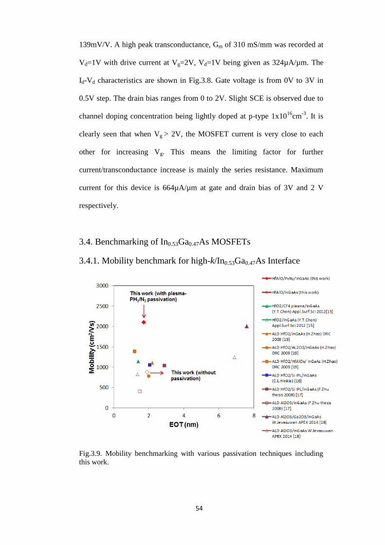
54
139mV/V. A high peak transconductance, Gm of 310 mS/mm was recorded at
Vd=1V with drive current at Vg=2V, Vd=1V being given as 324µA/µm. The
Id-Vd characteristics are shown in Fig.3.8. Gate voltage is from 0V to 3V in
0.5V step. The drain bias ranges from 0 to 2V. Slight SCE is observed due to
channel doping concentration being lightly doped at p-type 1x10¹⁶
cm-3
. It is
clearly seen that when Vg > 2V, the MOSFET current is very close to each
other for increasing Vg. This means the limiting factor for further
current/transconductance increase is mainly the series resistance. Maximum
current for this device is 664µA/µm at gate and drain bias of 3V and 2 V
respectively.
3.4. Benchmarking of In0.53Ga0.47As MOSFETs
3.4.1. Mobility benchmark for high-k/In0.53Ga0.47As Interface
Fig.3.9. Mobility benchmarking with various passivation techniques including
this work.

55
The mobility value obtained for this work has been benchmarked
against several passivation techniques which include CF4 plasma [15], Si [16-
17], Ga2O3 [18] and HfO2/HfAlO bi-layer gate stack [19] shown in Fig.3.9.
Mobility obtained for this work is similar to the best reported surface-channel
mobility, and highest compared to the rest for an aggressively scaled EOT.
This is attributed to better passivation and the smaller channel doping
concentration of 1x10¹⁶
cm-3
for this work, while the rest corresponds to larger
channel doping concentration of 3x10¹⁶
cm-3
[18], 5x10¹⁶
cm-3
[15], 1x10¹⁷
cm-3
[16], 3x10¹⁷
cm-3
[17]. In addition, mobility benchmarking shows that
passivation layers or bi-layer gate oxide would result in larger mobility due to
reduced trap density.
3.4.2. Dit benchmark for high-k/In0.53Ga0.47As Interface
Fig.3.10. Dit (taken at E-Ei=0.25eV) as a function of EOT for devices with
different passivation or bi-layer gate oxide.

56
The benchmark of Dit taken at trap energy levels of 0.25eV away from
intrinsic Fermi level vs EOT, depicted in Fig.3.10, shows that for all
references including this work, bi-layer gate oxide or gate oxide with
interfacial layers are needed for reduced Dit required for device enhancement.
Energy levels close to the conduction band is taken for comparison because
mobility and hence device performance in on-state is mainly attributed to Dit
in this range [21-22]. In addition, figure shows that even at scaled EOT of
1.7nm, small Dit in the low 2.5x10¹²
cm-2
eV-1
is achievable in our work, which
is comparable to those best few reported in literature. Ref [15] and Ref [19]
both gives lower Dit compared to this work due to gate last process being
adopted for their work, in order to protect gate stack from S/D annealing.
Note that for Ref [18], the Dit is significantly smaller but yet in the mobility
results, it is comparable to that obtained as this work. This is likely due to the
Dit measured taken from MOSCAP instead of MOSFET, which excludes the
effect from the high temperature S/D annealing thus underestimating the Dit.
This implies the concept of plasma-PH3/N2 is appealing for future gate-first
self-aligned In0.53Ga0.47As MOS device due to its Dit being of comparable
values to that of gate-last processes.
3.4.3. Id,sat benchmark for high-k/In0.53Ga0.47As Interface
Id,sat for comparison has been taken at gate overdrive of Vg-Vt,sat=1.5V,
Vd=1V to remove the effects of SCE for fair benchmarking as shown in
Fig.3.11. The drain current achieved in our self-aligned gate-first 3µm
plasma-PH3/N2 passivated HfAlO/In0.53Ga0.47As MOSFET is higher than that
of a 1µm ALD Al2O3/In0.53Ga0.47As MOSFET from Ref [23]. This is due to
the smaller channel doping concentration used in our work given by

57
1x10¹⁶
cm-3
compared to 5x10¹⁶
cm-3
used in Ref [23]. In addition, the 0.8µm
and 0.6µm plasma-PH3/N2 passivated devices fabricated in this work also
both show larger Id,sat than the 0.5µm device fabricated in Ref [25], which
makes use of gate-last process in Ref [25]. The fact that this work shows
comparable results with gate last ALD-Al2O3 process further confirms the
good thermal stability of device fabricated with plasma-PH3/N2 passivation
technique.
On the other hand, it is observed that gate first self-aligned process
using in-situ ultrahigh vacuum MBE deposition technique to deposit the
Al2O3/GGO i.e. Ga2O3 (Gd2O3) in Ref [23] gives larger Id,sat than ALD
deposited Al2O3/In0.53Ga0.47As [23] and also our work. This is due to the clean
GGO/In0.53Ga0.47As interface, free of In2O3, In (OH)3, and Ga2O3 but still
observed in the ALD approach [28-29]. For our work, as will be mentioned in
Section 5.2.3.3, due to their smaller binding energy separation between the
peaks and the XPS lines of Ga3d and In4d being strongly overlapped with
Hf4f (since our gate dielectric is HfAlO), it is difficult to deconvolute the
peaks from oxides of Ga and In. However, as shown in Fig.5.9, we compare
the change in Ga/In ratio using angle-resolved XPS (ARXPS), with respect to
with and without RTP to deduce the passivation effect on the chemical
composition disturbance at the oxide/In0.53Ga0.47As interface. Although we
could not indicate what species were formed exactly at the
HfAlO/In0.53Ga0.47As interface, we found that the chemical disturbance in
relative Ga/In ratios of In0.53Ga0.47As by the RTP is still present, though
significantly reduced at the interface with the plasma-PH3/N2 passivation.
Therefore this disturbance of the Ga/In ratio, which signifies a chemical
reaction occurring at the HfAlO/In0.53Ga0.47As interface, explains the reason
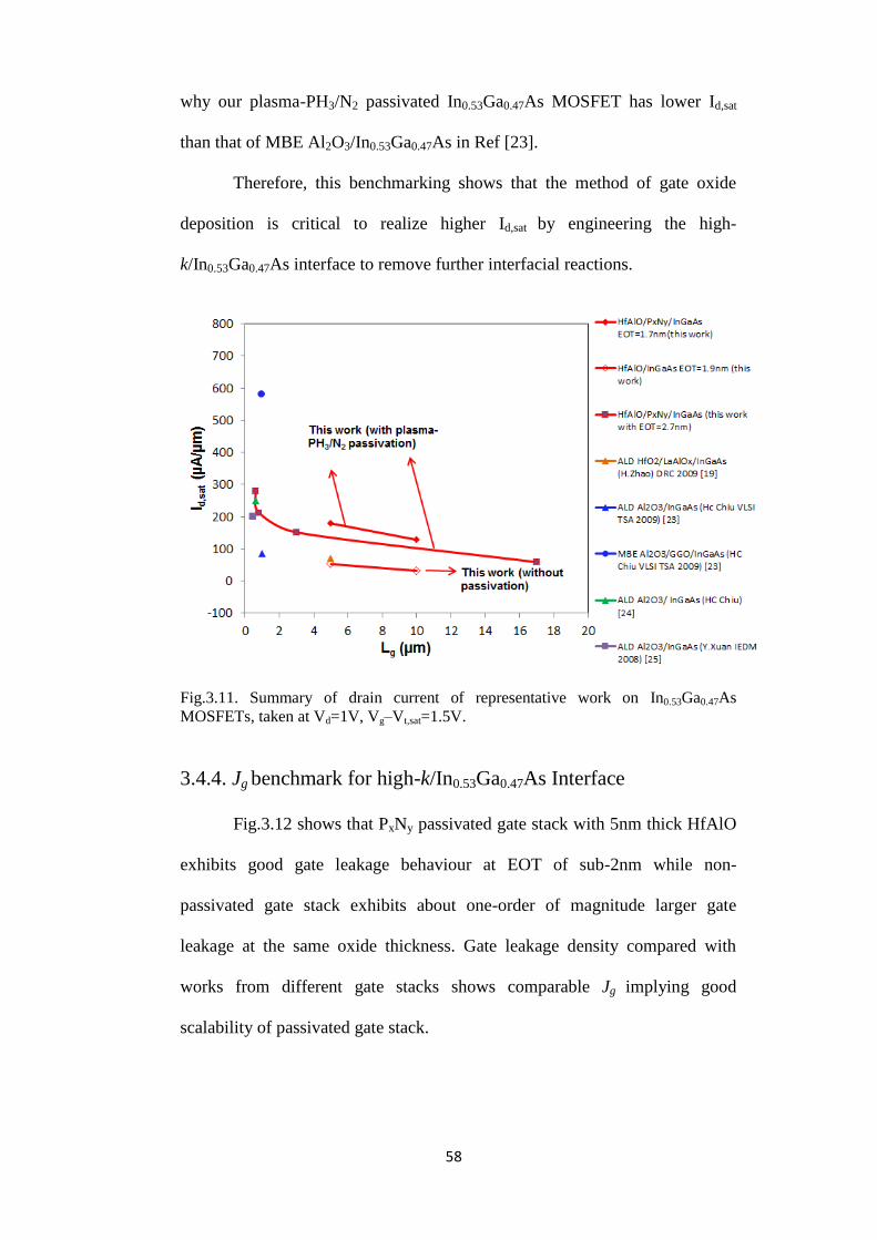
58
why our plasma-PH3/N2 passivated In0.53Ga0.47As MOSFET has lower Id,sat
than that of MBE Al2O3/In0.53Ga0.47As in Ref [23].
Therefore, this benchmarking shows that the method of gate oxide
deposition is critical to realize higher Id,sat by engineering the high-
k/In0.53Ga0.47As interface to remove further interfacial reactions.
Fig.3.11. Summary of drain current of representative work on In0.53Ga0.47As
MOSFETs, taken at Vd=1V, Vg–Vt,sat=1.5V.
3.4.4. Jg benchmark for high-k/In0.53Ga0.47As Interface
Fig.3.12 shows that PxNy passivated gate stack with 5nm thick HfAlO
exhibits good gate leakage behaviour at EOT of sub-2nm while non-
passivated gate stack exhibits about one-order of magnitude larger gate
leakage at the same oxide thickness. Gate leakage density compared with
works from different gate stacks shows comparable Jg implying good
scalability of passivated gate stack.
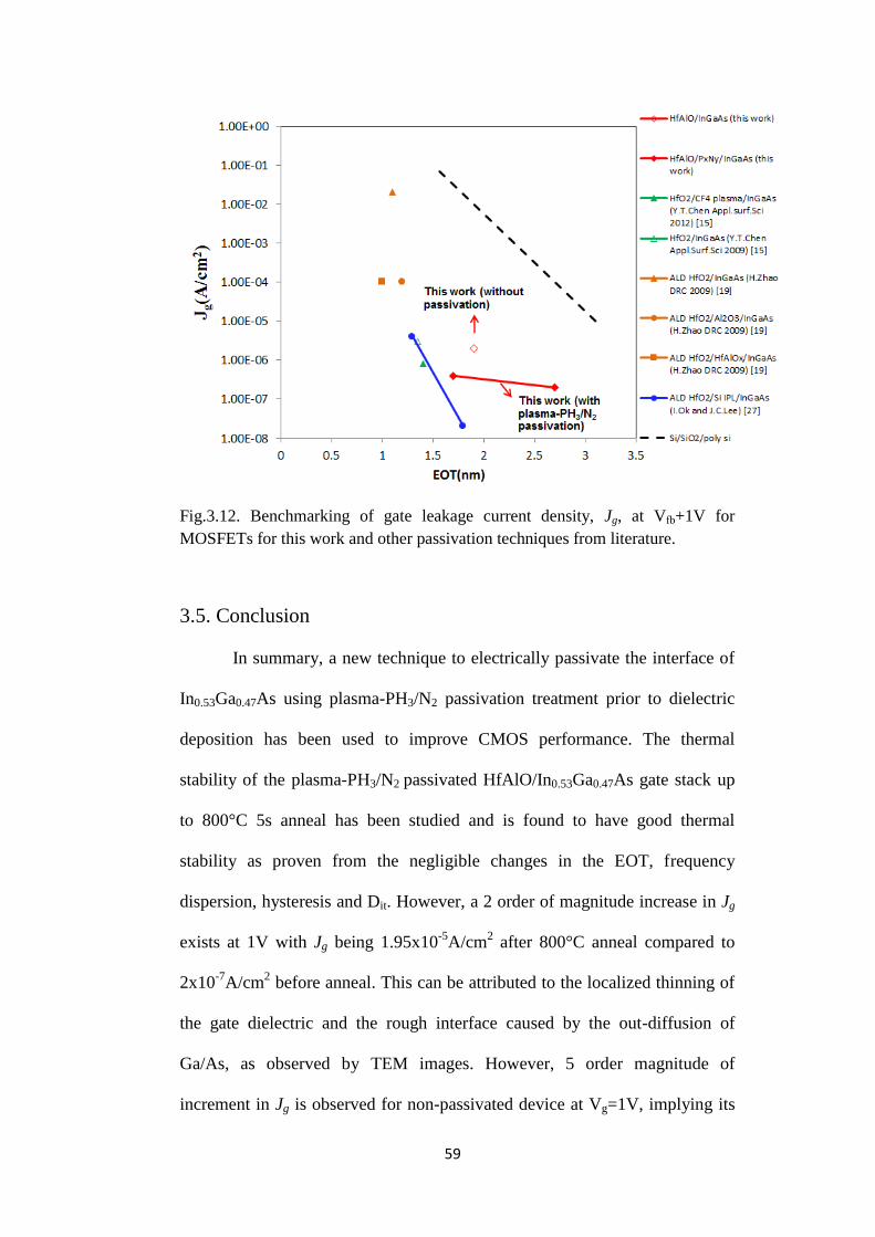
59
Fig.3.12. Benchmarking of gate leakage current density, Jg, at Vfb+1V for
MOSFETs for this work and other passivation techniques from literature.
3.5. Conclusion
In summary, a new technique to electrically passivate the interface of
In0.53Ga0.47As using plasma-PH3/N2 passivation treatment prior to dielectric
deposition has been used to improve CMOS performance. The thermal
stability of the plasma-PH3/N2 passivated HfAlO/In0.53Ga0.47As gate stack up
to 800°C 5s anneal has been studied and is found to have good thermal
stability as proven from the negligible changes in the EOT, frequency
dispersion, hysteresis and Dit. However, a 2 order of magnitude increase in Jg
exists at 1V with Jg being 1.95x10⁻⁵
A/cm2 after 800°C anneal compared to
2x10⁻⁷
A/cm2 before anneal. This can be attributed to the localized thinning of
the gate dielectric and the rough interface caused by the out-diffusion of
Ga/As, as observed by TEM images. However, 5 order magnitude of
increment in Jg is observed for non-passivated device at Vg=1V, implying its

60
worse thermal stability than passivated device. Dit measurement by the
charge-pumping method and SS results revealed consistent values with
increase in temperature for plasma-PH3/N2 passivated devices, implying good
thermal stability. Device characteristics of Lg=600nm for
HfAlO/PxNy/In0.53Ga0.47As MOSFET has been reported, in addition to
benchmarking of Dit, mobility, Id,sat and Jg with respect to other passivation
techniques.
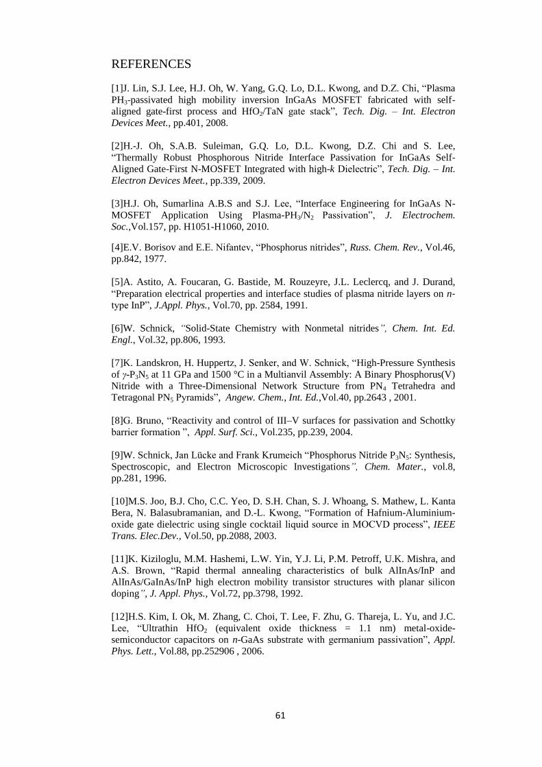
61
REFERENCES
[1]J. Lin, S.J. Lee, H.J. Oh, W. Yang, G.Q. Lo, D.L. Kwong, and D.Z. Chi, “Plasma
PH3-passivated high mobility inversion InGaAs MOSFET fabricated with self-
aligned gate-first process and HfO2/TaN gate stack”, Tech. Dig. – Int. Electron
Devices Meet., pp.401, 2008.
[2]H.-J. Oh, S.A.B. Suleiman, G.Q. Lo, D.L. Kwong, D.Z. Chi and S. Lee,
“Thermally Robust Phosphorous Nitride Interface Passivation for InGaAs Self-
Aligned Gate-First N-MOSFET Integrated with high-k Dielectric”, Tech. Dig. – Int.
Electron Devices Meet., pp.339, 2009.
[3]H.J. Oh, Sumarlina A.B.S and S.J. Lee, “Interface Engineering for InGaAs N-
MOSFET Application Using Plasma-PH3/N2 Passivation”, J. Electrochem.
Soc.,Vol.157, pp. H1051-H1060, 2010.
[4]E.V. Borisov and E.E. Nifantev, “Phosphorus nitrides”, Russ. Chem. Rev., Vol.46,
pp.842, 1977.
[5]A. Astito, A. Foucaran, G. Bastide, M. Rouzeyre, J.L. Leclercq, and J. Durand,
“Preparation electrical properties and interface studies of plasma nitride layers on n‐type InP”, J.Appl. Phys., Vol.70, pp. 2584, 1991.
[6]W. Schnick, “Solid-State Chemistry with Nonmetal nitrides”, Chem. Int. Ed.
Engl., Vol.32, pp.806, 1993.
[7]K. Landskron, H. Huppertz, J. Senker, and W. Schnick, “High-Pressure Synthesis
of γ-P3N5 at 11 GPa and 1500 °C in a Multianvil Assembly: A Binary Phosphorus(V)
Nitride with a Three-Dimensional Network Structure from PN4 Tetrahedra and
Tetragonal PN5 Pyramids”, Angew. Chem., Int. Ed.,Vol.40, pp.2643 , 2001.
[8]G. Bruno, “Reactivity and control of III–V surfaces for passivation and Schottky
barrier formation ”, Appl. Surf. Sci., Vol.235, pp.239, 2004.
[9]W. Schnick, Jan Lücke and Frank Krumeich “Phosphorus Nitride P3N5: Synthesis,
Spectroscopic, and Electron Microscopic Investigations”, Chem. Mater., vol.8,
pp.281, 1996.
[10]M.S. Joo, B.J. Cho, C.C. Yeo, D. S.H. Chan, S. J. Whoang, S. Mathew, L. Kanta
Bera, N. Balasubramanian, and D.-L. Kwong, “Formation of Hafnium-Aluminium-
oxide gate dielectric using single cocktail liquid source in MOCVD process”, IEEE
Trans. Elec.Dev., Vol.50, pp.2088, 2003.
[11]K. Kiziloglu, M.M. Hashemi, L.W. Yin, Y.J. Li, P.M. Petroff, U.K. Mishra, and
A.S. Brown, “Rapid thermal annealing characteristics of bulk AlInAs/InP and
AlInAs/GaInAs/InP high electron mobility transistor structures with planar silicon
doping”, J. Appl. Phys., Vol.72, pp.3798, 1992.
[12]H.S. Kim, I. Ok, M. Zhang, C. Choi, T. Lee, F. Zhu, G. Thareja, L. Yu, and J.C.
Lee, “Ultrathin HfO2 (equivalent oxide thickness = 1.1 nm) metal-oxide-
semiconductor capacitors on n-GaAs substrate with germanium passivation”, Appl.
Phys. Lett., Vol.88, pp.252906 , 2006.

62
[13]G. Groeseneken, H.E. Maes, N. Beltran, and R.F. Dekeersmaecker, "A Reliable
Approach to Charge-pumping Measurements in MOS-Transistors", IEEE Trans.
Elec.Dev., Vol. 31, pp. 42-53, 1984.
[14]R. Xie, N. Wu, C. Shen, and C. Zhu, “Energy distribution of interface traps in
germanium metal-oxide-semiconductor field effect transistors with HfO2 gate
dielectric and its impact on mobility”, Appl. Phys. Lett., Vol.93, pp.083510, 2008.
[15]Y.T. Chen, Y. Wang, F. Xue, F. Zhou and J.C. Lee, “Optimization of Fluorine
Plasma Treatment for Interface Improvement on HfO2/In0.53Ga0.47As MOSFETs”,
App.Sci, Vol.2, pp.233, 2012.
[16]C L. Hinkle, A.M. Sonnet, R.A. Chapman, and E.M. Vogel, “Extraction of the
Effective Mobility of In0.53Ga0.47As MOSFETs”, IEEE Ele.Dev.Lett, Vol.30, No.4,
pp.316, 2009.
[17]F. Zhu, “Investigation of electrical characteristics of III-V MOS devices with
silicon interface passivation layer”, PhD Dissertation, Univ.of Texas at Austin, 2008.
[18]W. Jevasuwan, T. Maeda, N. Miyata, M. Oda, T. Irisawa, T. Tezuka, and T.
Yasuda, “Self-limiting growth of ultrathin Ga2O3 for the passivation of
Al2O3/InGaAs interfaces”, Applied Physics Express, Vol.7,pp. 011201, 2014.
[19]H. Zhao, Y. Chen, J. Yum, Y. Wang and J. C. Lee, “HfO2-Based In0.53Ga0.47As
MOSFETs (EOT~10Å) Using Various Interfacial Dielectric Layers”, IEEE Dev. Res.
Conf., pp.89, 2009.
[20]J. Huang, N. Goel, H. Zhao, C. Y. Kang, K.S. Min, G. Bersuker, S. Oktyabrsky,
C.K. Gaspe, M.B. Santos, P. Majhi, P.D. Kirsch, H.-H. Tseng, J.C. Lee, and R.
Jammy, “InGaAs MOSFET Performance and Reliability Improvement by
Simultaneous Reduction of Oxide and Interface Charge in ALD (La)AlOx/ZrO2 Gate
Stack”, Tech. Dig. – Int. Electron Devices Meet., 2009, pp.338.
[21]A. Ali, H. Madan, S. Koveshnikov and S. Datta, “Small Signal Response of
Inversion Layers in High Mobility In0.53Ga0.47As MOSFETs Made with Thin high-k
Dielectrics”, IEEE Trans. Ele. Dev., Vol. 57, pp. 742-748, 2010.
[22]N. Miyata, H. Ishii, Y.Urabe, T. Itatani, T. Yasuda, H. Yamada, N. Fukuhara,
M.Hata, M. Deura, M. Sugiyama, M. Takenaka, S. Takagi, “Origin of electron
mobility enhancement in (111)-oriented InGaAs channel metal–insulator–
semiconductor field-effect-transistors”, Microelectronic.Eng., Vol.88, pp.3459–3461,
2011.
[23]H.C. Chiu, T.D. Lin, P. Chang, W.C. Lee, C.H. Chiang, J. Kwo, Y.S. Lin, S.H.
Hsu, W. Tsai, and M. Hong , “Self-aligned Inversion Channel In0.53Ga0.47As N-
MOSFETs with ALD- Al2O3 and MBE- Al2O3/ Ga2O3 (Gd2O3) as Gate Dielectrics”,
VLSI-TSA, pp.141, 2009.
[24]H.C. Chiu, P. Chang, M.L. Huang, T.D. Lin, Y.H. Chang, J.C. Huang, S.Z.
Chen, J. Kwo, “High performance self-aligned inversion-channel MOSFETs with
In0.53Ga0.47As channel and ALD- Al2O3 gate dielectric”, IEEE Dev.Res.Conf., pp.83,
2009.
[25]Y. Xuan, Y.Q. Wu, T. Shen, T. Yang, and P.D. Ye, “High performance
submicron inversion-type enhancement-mode InGaAs MOSFETs with ALD Al203,

63
HfO2 and HfAlO as gate dielectrics”, Tech. Dig. – Int. Electron Devices Meet.,
pp.637, 2007.
[26]T.D. Lin, W.H. Chang, R.L. Chu , Y.C. Chang, Y.H. Chang, M.Y. Lee, P.F.
Hong, M.C. Chen, J. Kwo and M. Hong , “High-performance self-aligned inversion-
channel In0.53Ga0.47As metal-oxide-semiconductor field-effect-transistors by in-situ
atomic-layer-deposited HfO2”, Appl.Phys.Lett., Vol.103, pp.253509, 2013.
[27]S. Oktyabrsky and P.D. Ye, “Fundamentals of III-V Semiconductor MOSFETs”
from book Chapter 11, I.Ok and J.C.Lee “Electrical and Material Characteristics of
Hafnium Oxide with Silicon Interface Passivation on III-V Substrate for Future
Scaled CMOS Technology” pp.341.
[28]M.L. Huang, Y.C. Chang, C.H. Chang, Y.J. Lee, P. Chang, J. Kwo, T.B. Wu,
and M. Hong, “Surface passivation of III-V compound semiconductors using atomic-
layer-deposition-grown Al2O3”, Appl.Phys.Lett., Vol. 87, pp. 252104, 2005.
[29]K.H. Shiu, T.H. Chiang, P. Chang, L.T. Tung, M. Hong, J. Kwo and W. Tsai,
“1nm equivalent oxide thickness in Ga2O3(Gd2O3)/In0.2Ga0.8As metal-oxide-
semiconductor capacitors”, Appl. Phys. Lett., Vol.92, pp.172904, 2008

64
Chapter 4: Leakage Current and Carrier Transport
Mechanisms of plasma-PH3/N2 Passivated HfAlO/
In0.53Ga0.47As MOSFET
4.1. Introduction and Motivation
From the previous chapter, we have studied the thermal stability
performance of the HfAlO/In0.53Ga0.47As MOSFET and shown the
improvements made in the device characteristics with plasma-PH3/N2
passivation treatment. However, understanding of how this treatment is
effective in improving the device performance in terms of the various
mechanisms such as gate leakage, off-state leakage and carrier transport
mechanism have yet to be investigated systematically. Detailed knowledge of
gate leakage and carrier transport can give insight to defects that are present in
the high-k oxide or at the high-k/In0.53Ga0.47As interface, and thus allows
targeted improvement to be made to the gate stack.
The aim of this chapter is to investigate the physical origins of the gate
leakage improvement and improvement in off-state leakage and carrier-
transport mechanism in the subthreshold and on-state of plasma-PH3/N2
passivated TaN/HfAlO/In0.53Ga0.47As MOSFETs compared to non-passivated
TaN/HfAlO/In0.53Ga0.47As MOSFETs, for temperatures between 250K and
420K. This is needed in order to investigate material parameters such as
activation energy of the traps and average bulk trap concentration as well
as distinguish the conduction mechanisms that contribute to the conduction
current through the dielectric film. Note that Chapter 4 and Chapter 5 have
results taken from the same device samples. Hence, discussions on them are
inter-related.
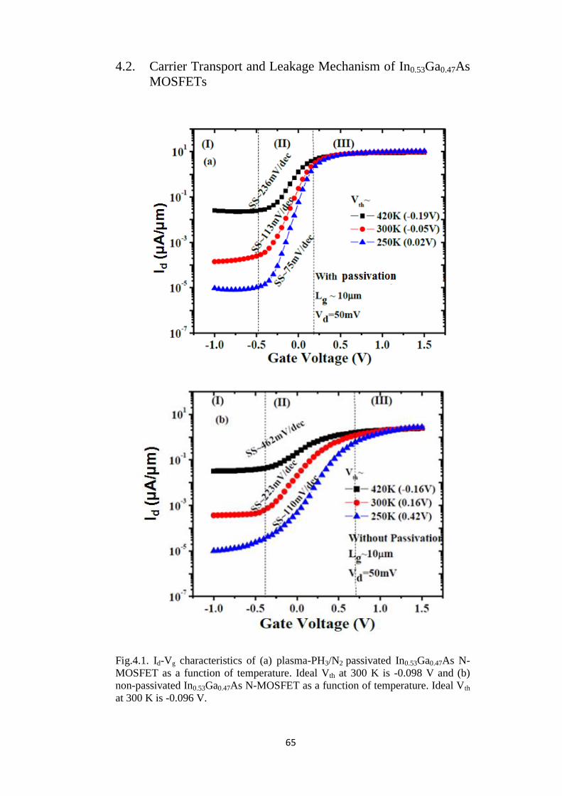
65
4.2. Carrier Transport and Leakage Mechanism of In0.53Ga0.47As
MOSFETs
Fig.4.1. Id-Vg characteristics of (a) plasma-PH3/N2 passivated In0.53Ga0.47As N-
MOSFET as a function of temperature. Ideal Vth at 300 K is -0.098 V and (b)
non-passivated In0.53Ga0.47As N-MOSFET as a function of temperature. Ideal Vth
at 300 K is -0.096 V.
75

66
4.2.1. Carrier Transport and Off-state Leakage Mechanism
In this chapter as well as Chapter 5, after completion of device
fabrication, gate leakage and Id-Vg measurements between 250K and 420K
have been performed on the devices to carry out the temperature dependence
studies. The temperature dependent drain current vs gate voltage (Id-Vg)
characteristics of the device with varying temperature from 250K to 420K
have been plotted out as shown in Fig.4.1(a) and 4.1(b). The temperature
dependence of the transfer characteristics is a strong function of gate bias,
indicating onset of various conduction mechanisms.
Figs.4.1(a)-(b) are divided into three regions. Region (I) will be used
to explain the Ioff contributors in the passivated and non-passivated
MOSFETs. Region (II) which corresponds to the subthreshold characteristics
will be used to analyse the impact of Dit present at the high-k
dielectric/In0.53Ga0.47As interface of passivated and non-passivated
In0.53Ga0.47As N-MOSFETs. Finally Region (III) will be used to explain the
carrier transport mechanism for both non-passivated and passivated devices.
The Ioff contributors in the N-MOSFETs shown from Region (I) in
Figs.4.1(a)-(b) have been evaluated as shown in Fig.4.2. The reverse biased
drain-substrate p-n junction current, Ibulk, is the significant contributor to Ioff
for both passivated and non-passivated devices. This reverse biased junction
leakage current is a summation of the diffusion current, generation current
and band-to-band tunnelling current [1].
To understand the mechanism of this reverse biased p-n junction
leakage which is strongly dependent on temperature, the readings taken at
Vg=-0.7V within Region (I) of Figs.4.1(a)-(b), have been plotted as Ibulk in the
Arrhenius plot of the Ioff shown in Fig.4.3. Only temperatures between 250K
67
and 300K were investigated for this analysis in order to prevent Ig from
dominating Ioff. This figure reveals a thermionic component with an
activation energy barrier Ea of 0.4eV for non-passivated and 0.38eV for
passivated N-MOSFETs, which is consistent with half the bandgap Eg/2 of
In0.53Ga0.47As. This strong temperature dependence indicates that band–to-
band tunneling (BTBT) component is negligible here. This Ea being equal to
Eg/2 indicates that the main contribution to the temperature dependence of
leakage floor is attributed to Shockley Read Hall generation-recombination
which is proportional to exp(-Eg/2kT), where Eg is the bandgap, k is the
Boltzmann constant and T is temperature.
SRH generation-recombination mechanism relies on the presence of
deep levels in the depletion region. It occurs when an electron trapped in a
deep level, gains energy, and climbs out of the Coulombic well. Hence, this
means that the junction leakage could come from the bulk defects caused by
the elements from the relatively volatile V group which is dependent on the
activation and implant condition. This is found to be the limitations of
implanted S/D In0.53Ga0.47As long channel MOSFETs observed by other
groups as well [2-3]. Hence, optimization has to be carried out on the implant
condition and activation anneal in order to further reduce the reverse biased
drain-substrate leakage but this component still has leakage floor
contributions. Thus, it is beneficial to study on non-implanted S/D
In0.53Ga0.47As MOSFET such as epitaxially grown S/D In0.53Ga0.47As
MOSFET or Implant Free MOSFET structures.

68
Fig.4.2. Four-terminal Id-Vg measurements on plasma-PH3/N2 passivated
In0.53Ga0.47As N-MOSFET showing Ioff dominated by Ibulk, known as reverse
biased drain-substrate junction leakage.
Fig.4.3. Temperature dependence of substrate current (Ibulk) of both plasma-
PH3/N2 passivated and non-passivated In0.53Ga0.47As N-MOSFET taken from
temperatures between 300K to 250K. The Ibulk values have been taken at Ioff
values at Vg=-0.7V from Fig.4.1(a) and 4.1(b). An activation energy of Eg/2
extracted in Region (I) confirms SRH generation-recombination current.

69
The impact of Dit present at the high-k dielectric/In0.53Ga0.47As
interface on the subthreshold characteristics [Region (II)] from Figs.4.1(a)-
(b), of passivated and non-passivated In0.53Ga0.47As N-MOSFETs will be
analysed here. It is seen that the average SS increases from 75mV/dec to
236mV/dec for plasma-PH3/N2 passivated device, while it increases from
110mV/dec to 462mV/dec for non-passivated device as temperature
increases. The expression for the SS is given by SS=[2.3kT/q]*[1+
(Cd+Cit)/Cox] where Cox is the oxide capacitance and Cd is the semiconductor
depletion layer capacitance and Cit is the capacitance due to interface states.
The Dit (taken from Cit/q) obtained from experimental SS for 300K is
around 4.3x10¹²
cm-2
eV-1
for plasma-PH3/N2 passivated device and
1.5x10¹³
cm-2
eV-1
for non-passivated device. This means that plasma-PH3/N2
is also effective in improving the midgap Dit as seen from the improvements
in SS. In addition, from Fig.4.1(a), the Vth shift w.r.t. ideal Vth is not as
significant compared to the Vth shift w.r.t. ideal Vth of the non-passivated
device shown in Fig.4.1(b). This means that the passivated device consists of
smaller amounts of acceptor-like traps within the bandgap, while non-
passivated device consists of higher concentration of acceptor-like traps
which increases the Vth due to negative charging of these acceptor states [4].

70
Fig.4.4. ln|Id| vs ln|T| plot of both plasma-PH3/N2 passivated and non-passivated
In0.53Ga0.47As N-MOSFET showing a negative temperature dependence of the
on-current.
In Region (III) of Figs.4.1(a)-4.1(b), Ion is seen to be larger in the
passivated than non-passivated device caused by the lesser contribution from
acceptor-like traps in the upper half of the bandgap which causing lesser
amount of negative trapped charges to be built in when EF sweeps to the Ec
[5] This further confirms the larger concentration of acceptor-like traps in
non-passivated device compared to passivated device.
In addition, discussing the carrier transport mechanism of the non-
passivated and plasma-PH3/N2 passvated device, it is observed that Id
increases as temperature decreases for both passivated and non-passivated
device, with Id having temperature dependence of T-0.37
for passivated device,
which is stronger than that of non-passivated device having temperature
dependence given by T-0.18
as shown in Fig.4.4. The weaker temperature
dependence for non-passivated device implies its mobility degradation
mechanism is being dominated by interface dipole or surface roughness
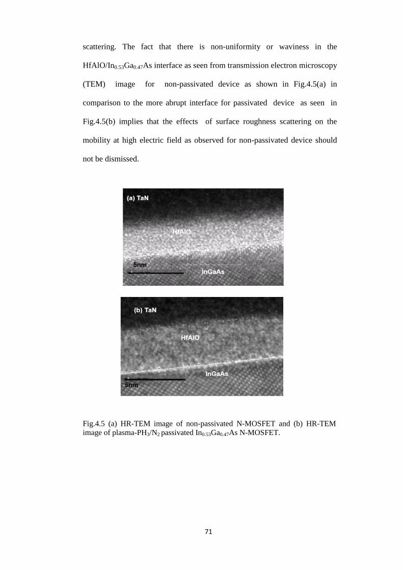
71
scattering. The fact that there is non-uniformity or waviness in the
HfAlO/In0.53Ga0.47As interface as seen from transmission electron microscopy
(TEM) image for non-passivated device as shown in Fig.4.5(a) in
comparison to the more abrupt interface for passivated device as seen in
Fig.4.5(b) implies that the effects of surface roughness scattering on the
mobility at high electric field as observed for non-passivated device should
not be dismissed.
(a) TaN
HfAlO
I
Fig.4.5 (a) HR-TEM image of non-passivated N-MOSFET and (b) HR-TEM
image of plasma-PH3/N2 passivated In0.53Ga0.47As N-MOSFET.

72
4.2.2. Gate-leakage mechanism
4.2.2.1. Jg-Vg Characteristics at 300 K
Fig.4.6 illustrates the Jg of non-passivated and passivated
HfAlO/In0.53Ga0.47As N-MOSFETs described as a function of applied gate
voltage (Vg) in the substrate injection region at 300K. It is seen that
passivated device has lower Jg in the inversion region of N-MOSFET
compared to non-passivated device, especially in the Vg region greater than
1V. This could be due to the lower interface states and bulk traps in the
oxides of the passivated devices. It is seen from intercept of the EOT vs
physical oxide thickness shown in Fig.4.7 and high-resolution TEM (HR-
TEM) images of non-passivated and passivated device as shown in Fig.4.5(a)
and 4.5(b) respectively that the interfacial layer is thicker (~0.6nm) in
passivated than non-passivated (~0.35nm) device. However, the thicker
interfacial layer of passivated device compared to non-passivated device is
believed to be contributed mostly by the passivation layer which consists of
PxNy and P-for-As exchange layer [6]. On the other hand non-passivated
device interfacial layer is made up of the interdiffusion of elemental In/Ga
across the high-k/In0.53Ga0.47As interface and thus has low k values. Hence,
this also explains the larger EOT of 1.9nm for non-passivated compared to
1.7nm for passivated device despite the thicker interfacial layer of passivated
device.
The inset of Fig.4.6, which shows the lnǀJgǀ vs ln ǀEǀ plots for the two
types of device at positive gate bias and where E is the Electric field applied,
are investigated to analyze the conduction mechanism at 300 K. In low
electric field region (in the Ohmic regime i.e. V < VTR), Jg-Vg characteristics
followed the Ohm’s law where both passivated and non-passivated devices

73
show similar trends in leakage current i.e. J V s, where s refers to the slope
of the graph. The curves are linear with s~1 indicating an Ohmic behaviour,
with non-passivated device having s~0.92 while passivated device has
s~0.76. Ohm’s law implies that the density of thermally generated free
carriers inside the films is larger than the injected carriers due to the carrier
transit time (τc) being larger than the dielectric relaxation time (τd). Clearly,
this mechanism dominates behaviour of passivated devices throughout at
room temperature.
Fig.4.6. Jg characteristics of plasma-PH3/N2 passivated and non-passivated
In0.53Ga0.47As N-MOSFET at 300 K. Inset shows the lnǀJgǀ vs lnǀEǀ plot. EOT
value of non-passivated In0.53Ga0.47As N-MOSFET is 1.9 nm and EOT value of
passivated In0.53Ga0.47As N-MOSFET is 1.7 nm. The voltage boundaries and s
values of JVs fits are also shown.

74
Fig.4.7. EOT vs physical oxide thickness of both passivated and non-passivated
devices.
The non-passivated device shows Voltage Square Law and Trap
Filled Limited Regimes (TFL) [7-8] determined by higher s due to space
charge limited conduction (SCLC) mechanism. In the inset of Fig.4.6, the
region between VTR and VTFL is referred to as the Voltage Square Law
regime. The onset voltage VTR can be expressed as Equation (4.1) [7]:
where no is the concentration of free charge carriers in equilibrium, d is the
thickness of the HfAlO film, εr is the dynamic dielectric constant of the
HfAlO film, εo is the permittivity of free space and θ refers to the ratio of
free-carrier density to total carrier (free and trapped) density. In this region
where V > VTR, τc becomes equal or less than τd. This means that the τc is too
short for dielectric relaxation to take place. Hence, the amount of injected
carriers will exceed the thermally generated carriers [9]. Thus, with
increasing Vg, more injected electrons would be supplied and then captured in
Equation (4.1)
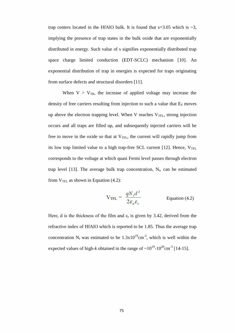
75
trap centers located in the HfAlO bulk. It is found that s=3.05 which is ~3,
implying the presence of trap states in the bulk oxide that are exponentially
distributed in energy. Such value of s signifies exponentially distributed trap
space charge limited conduction (EDT-SCLC) mechanism [10]. An
exponential distribution of trap in energies is expected for traps originating
from surface defects and structural disorders [11].
When V > VTR, the increase of applied voltage may increase the
density of free carriers resulting from injection to such a value that EF moves
up above the electron trapping level. When V reaches VTFL, strong injection
occurs and all traps are filled up, and subsequently injected carriers will be
free to move in the oxide so that at VTFL, the current will rapidly jump from
its low trap limited value to a high trap-free SCL current [12]. Hence, VTFL
corresponds to the voltage at which quasi Fermi level passes through electron
trap level [13]. The average bulk trap concentration, Nt, can be estimated
from VTFL as shown in Equation (4.2):
Here, d is the thickness of the film and εr is given by 3.42, derived from the
refractive index of HfAlO which is reported to be 1.85. Thus the average trap
concentration Nt was estimated to be 1.3x10¹⁹
cm-3
, which is well within the
expected values of high-k obtained in the range of ~1019
-1020
cm-3
[14-15].
Equation (4.2)
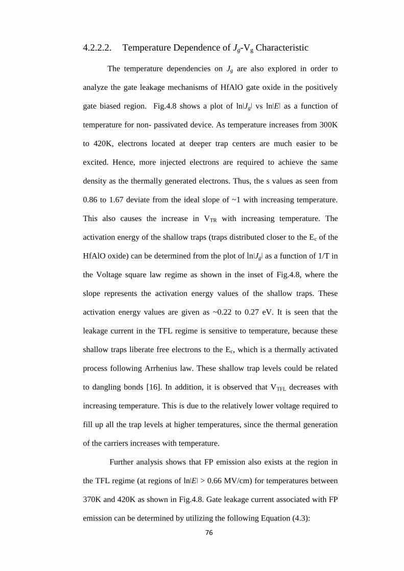
76
4.2.2.2. Temperature Dependence of Jg-Vg Characteristic
The temperature dependencies on Jg are also explored in order to
analyze the gate leakage mechanisms of HfAlO gate oxide in the positively
gate biased region. Fig.4.8 shows a plot of lnǀJgǀ vs lnǀEǀ as a function of
temperature for non- passivated device. As temperature increases from 300K
to 420K, electrons located at deeper trap centers are much easier to be
excited. Hence, more injected electrons are required to achieve the same
density as the thermally generated electrons. Thus, the s values as seen from
0.86 to 1.67 deviate from the ideal slope of ~1 with increasing temperature.
This also causes the increase in VTR with increasing temperature. The
activation energy of the shallow traps (traps distributed closer to the Ec of the
HfAlO oxide) can be determined from the plot of lnǀJgǀ as a function of 1/T in
the Voltage square law regime as shown in the inset of Fig.4.8, where the
slope represents the activation energy values of the shallow traps. These
activation energy values are given as ~0.22 to 0.27 eV. It is seen that the
leakage current in the TFL regime is sensitive to temperature, because these
shallow traps liberate free electrons to the Ec, which is a thermally activated
process following Arrhenius law. These shallow trap levels could be related
to dangling bonds [16]. In addition, it is observed that VTFL decreases with
increasing temperature. This is due to the relatively lower voltage required to
fill up all the trap levels at higher temperatures, since the thermal generation
of the carriers increases with temperature.
Further analysis shows that FP emission also exists at the region in
the TFL regime (at regions of lnǀEǀ > 0.66 MV/cm) for temperatures between
370K and 420K as shown in Fig.4.8. Gate leakage current associated with FP
emission can be determined by utilizing the following Equation (4.3):

77
Where Nc is the density of states in the conduction band, µ is the
mobility, qt is the trap energy level, E is the electric field and r is the
dynamic dielectric constant. For FP emission the plot of ln(Jg/E) vs E1/2
should
be linear, with the slope corresponding to the inverse of the r of the gate
dielectric. From the slopes of the two linear plots in Fig.4.9, the r values at
temperatures of 370K and 420K are found to be 5.2 and 2.4 respectively. These
values correspond to the same order of magnitude of r of HfAlO given by 3.42
reported in literature [17]. Hence, this means that FP emission also exists in
non-passivated device at high temperature and high field region.
The Arrhenius plot of ln (Jg/E) vs 1/T shown in the inset of Fig.4.9
reveals that the ionization energy of the traps (also means the energy barrier of
the traps with respect to Ec) within the HfAlO is given as ~0.95 to 1.3 eV
below Ec. The fact that the activation energy obtained from the Arrhenius plot
of voltage square law regime in the given temperature range is significantly
smaller than the trap energy estimated from FP Arrhenius plot indicates that
the traps responsible for these two mechanisms are different. FP conduction
should originate from the deeper trap levels in the oxide, such as interstitial
defects [18-20] or vacancies. On the other hand, SCLC mechanism is due to
the shallow trap levels, attributed to defects with energy levels close to Ec, such
as dangling bonds. As will be seen in Chapter 5, the existence of these defect
levels can be attributed to the interdiffusion of In/Ga elements across the
HfAlO/In0.53Ga0.47As interface as analyzed from XPS analysis.
Equation (4.3)
78
Fig.4.9. ln(Jg/E) vs E½ plots (FP fitting) observed in non-passivated In0.53Ga0.47As
N-MOSFET. Inset shows the Arrhenius plot in the FP emission regime.
Fig.4.8. ln|Jg| vs ln|E| plot of non-passivated device at temperatures between 250K
and 420K.Inset shows the Arrhenius plot in the TFL regime.
-1.5 -1.0 -0.5 0.0 0.5 1.0 1.5-18
-16
-14
-12
-10
-8
-6
-4
-2
0.0024 0.0026 0.0028 0.0030 0.0032 0.0034-15
-14
-13
-12
-11
-10
ln(J
g)
(A/c
m2
)
1/T (K-1)
ln(E) (MV/cm)
0.26 (Ea~0.22eV)
0.34 (Ea~0.23eV)
0.41 (Ea~0.24eV)
0.47 (Ea~0.24eV)
0.53 (Ea~0.25eV)
0.59 (Ea~0.27eV)
Arrhenius Plot in TFL regime 0.0024 0.0025 0.0026 0.0027-13
-12
-11
-10
-9
-8
-7
-6
-5
-4
-3
-2
-1
0
E1/2
(MV/cm)1/2
1.41
1.48
1.55
1.61
1.66
1.73
1/T (K-1)
ln(J
g/E
) (A
/MV
cm
)
Arrhenius plot for FP emission
Ea ~ 0.95-1.3 eV
s=6.
1
s=2.78
s=2.92
250K
300K
370K
420K
s=7.
6
s=1.67
s=1.34
s=5.
62
s=3.05
s=0.92
s=0.86
ln(J
g)
(A/c
m2)
ln(E) (MV/cm)
Without Passivation

79
On the other hand, Fig.4.10 which shows a plot for the passivated
device, depicts that the s values in the voltage square law regime are given as
~2 for 370K and 420K, suggesting a trap free SCLC mechanism, instead of
EDT-SCLC mechanism. This happens when the trap level is so shallow i.e.
having small ionization energy that they are not effective as electron traps. The
dominance of such mechanism means that there are less bulk oxide defects
present in the passivated device and that injection of carriers may also be
limited by the interface properties of the high-k/In0.53Ga0.47As, further implying
the existence of a well-formed interface between the HfAlO and In0.53Ga0.47As
which is in good agreement with the HRTEM image shown in Fig.4.5(b),
compared to non-passivated device. Also, in contrast to non-passivated device,
passivated device also does not experience TFL regime and FP emission,
further suggesting the advantages that plasma-PH3/N2 passivation has on
reducing these defects caused by interstitial defects or vacancies.
Fig.4.10. ln|Jg| vs ln|E| plot of plasma-PH3/N2 passivated In0.53Ga0.47As N-
MOSFET at temperatures between 250K and 420K.

80
4.3. Conclusion
As a conclusion, in Section 4.2.2, gate leakage mechanism of the
HfAlO plasma-PH3/N2 passivated and non-passivated In0.53Ga0.47As MOSFETs
have been evaluated, in order to correlate the quality of the oxide deposited
with the gate leakage mechanisms observed. It is found that at temperatures
higher than 300K, trap free SCLC mechanism dominates the gate leakage
of passivated device but non-passivated device consists of exponentially
distributed SCLC mechanism as well as Frenkel-Poole emission at high
electric field. This Frenkel-Poole emission is associated with energy trap levels
of ~0.95eV to 1.3eV and is responsible for the increased gate leakage of non-
passivated device. In addition, the electrical properties of the non-passivated
device has also been extracted from the SCLC mechanism, with the average
trap concentration of the shallow traps of 1.3x10¹⁹
cm-3
and their average
activation energy of ~0.22 to 0.27eV. The existence of these defect levels in
non-passivated device can be attributed to the interdiffusion of In/Ga/As
elements across the HfAlO/In0.53Ga0.47As interface, thus also affecting the trap
densities within the HfAlO. On the other hand, passivated device does not
contain Frenkel-Poole emission nor exponentially distributed SCLC
mechanism, indicating the absence of such defects in the bulk of the oxide. In
addition, the temperature dependent characteristics of off-state leakage have
also been evaluated to provide insight into the off-state mechanism shown in
Section 4.2.1. The off-state leakage of both passivated and non-passivated
device is determined by Ibulk where its terminology is described by reverse
biased drain-substrate junction leakage, with Shockley-Read-Hall mechanism
being its main contributor, and has activation energy of 0.38eV for passivated

81
device and 0.4eV for non-passivated device.

82
REFERENCES
[1]S.M. Sze and K.K. Ng, Physics of Semiconductor devices 3
rd ed, Wiley-blackwell
2007.
[2]Y.Q. Wu, M. Xu, R.S. Wang, O. Koybasi and P. D. Ye, “High Performance Deep-
Submicron Inversion-Mode InGaAs MOSFETs with maximum Gm exceeding 1.1
mS/μm: New HBr Pretreatment and Channel Engineering”, Tech. Dig. – Int. Electron
Devices Meet., pp.323, 2009.
[3]N. Goel, D. Heh, S. Koveshnikov, I. Ok ,S. Oktyabrsky, V. Tokranov, R.
Kambhampatic, M. Yakimov, Y. Sun, P. Pianetta, C.K. Gaspe, M.B. Santos, J. Lee, S.
Datta, P. Majhi, W. Tsai, “Addressing the gate stack challenge for high mobility
InxGa1-xAs channels for NFETs”, Tech. Dig. – Int. Electron Devices Meet., pp.1-4,
2008.
[4]D. Varghese, Y. Xuan, Y.Q. Wu, P.D. Ye, and M.A. Alam, “Multi-probe interface
characterization of In0.65Ga0.35As/ Al2O3 MOSFET”, Tech. Dig. – Int. Electron Devices
Meet., pp. 379, 2008.
[5]Y. Xuan, P.D. Ye, and T. Shen, “Substrate engineering for high-performance
surface-channel III-V metal-oxide-semiconductor field-effect transistors”, Appl. Phys.
Lett., Vol.91, pp.232107, 2007.
[6]H.J. Oh, Sumarlina A.B.S and S.J. Lee, “Interface Engineering for InGaAs n-
MOSFET Application Using Plasma PH3–N2 Passivation”, J. Electrochem., Soc., Vol.
157, No. 11, pp. H1051-H1060, 2010.
[7]M.A. Lampert, “Simplified Theory of Space Charge Limited Currents in an
Insulator with Traps”, Phys.Rev., Vol.103, p.1648, 1956.
[8]A. Rose, “Space-Charge-Limited Currents in Solids”, Phys.Rev., Vol.97, pp.1538,
1955.
[9]M.A. Lampert and P. Mark: Current Injection in Solids (Academic Press, New
York, 1970).
[10]P. Mark and W. Helfrich, “Space‐Charge‐Limited Currents in Organic Crystals”,
J. Appl. Phys., Vol.33, pp. 205, 1962.
[11]S. Baidyaroy and P. Mark: “Analytical and experimental investigation of the
effects of oxygen chemisorption on the electrical conductivity of CdS”, Surf. Sci.,
Vol.30, pp.53, 1972.
[12]F.C. Chiu, S. Mondal and T.M. Pan, “High-k dielectrics for CMOS technology”,
Book chapter “Structual and electrical characteristics of alternative high-k dielectric
for CMOS application”, pp.111, 2011.
[13]F.C. Chiu, H.W. Chou, and J.Y.M. Lee, “Electrical conduction mechanisms of
metal/La2O3/Si structure”, J. Appl. Phys., Vol.97, pp.103503, 2005.
[14]H.C. Chiu, L.T. Tung, and M. Hong, “Achieving a low interfacial density of states
in atomic layer deposited Al2O3 on In0.53Ga0.47As”, Appl. Phys. Lett., Vol.93
pp.202903, 2008

83
[15]H.D. Xiong, “Characterization of electrically active defects in high-k gate
dielectrics by using low frequency noise and charge pumping measurements”,
Microelectron. Eng., Vol.84, pp.2230, 2007.
[16]K.B. Jinesh, Y. Lamy, E. Tois, and W.F.A. Besling, “Charge conduction
mechanisms of atomic-layer-deposited Er2O3 thin film”, Appl. Phys. Lett., Vol.94 ,
pp.252906, 2009.
[17]P.S. Das and A. Biswas, “Improved electrical and interfacial properties of RF
sputtered HfAlOx on n-GaAs with effective Si passivation”, Appl.Surf.Sci., Vol.256,
p.6618, 2010.
[18]G. Molas, M. Bocquet, J. Buckley, H. Grampeix, M. Gely, J. P. Colonna, C.
Licitra, N. Rochat, T. Veyront, X. Garros, F. Martin, P. Brianceau, V.Vidal, C.
Bongiorno, S. Lombardo, B. De Salvo, and S. Deleonibus, “Investigation of hafnium-
aluminate alloys in view of integration as interpoly dielectrics of future Flash
memories”, Solid-State Electron., Vol.51, pp.1540, 2007.
[19]K. Tse, D. Liu and J. Robertson, “Oxygen vacancies in high-k oxides”,
Microelectronic. Eng., Vol.84 , pp. 2028, 2007.
[20]K. Xiong, K. Tse, and J. Robertson,“Defect states in the high-dielectric-constant
gate oxide HfSiO4”, J. Appl. Phys. Vol.101, pp.024101, 2007

84
Chapter 5: Effects of plasma-PH3/N2 Passivation on Mobility
Degradation Mechanisms of In0.53Ga0.47As MOSFETs
5.1. Introduction and Motivation
Demonstration of In0.53Ga0.47As based MOSFETs fabricated with
various in-situ and ex-situ deposited high-k dielectrics, with and without
passivation layer, has been reported [1-4]. However, its channel mobility has
still been lower than the expected bulk mobility achievable in In0.53Ga0.47As
which shows research potential of further improvement in device interface to
maximize mobility.
In order to realize mobility enhancement, the scattering mechanisms
responsible for the mobility degradation must be understood. In this chapter,
we will take a closer look at the influence of plasma-PH3/N2 passivation on the
mobility characteristics of In0.53Ga0.47As MOSFETs. Firstly, mobility
extraction and correction technique used would be discussed in Section 5.2.1.
The evaluation of the temperature dependence study of the mobility on the
mobility degradation mechanisms present in plasma-PH3/N2 passivated
In0.53Ga0.47As MOSFETs as well as non-passivated MOSFETs would be
investigated and discussed in Section 5.2.2. Section 5.2.3 would involve
analysis on the factors causing the improvement in the mobility of the plasma-
PH3/N2 passivated In0.53Ga0.47As MOSFETs compared to the non-passivated.

85
5.2. Mobility of plasma-PH3/N2 Passivated In0.53Ga0.47As MOSFETs
5.2.1. Mobility Extraction and Correction Technique
In this work, we extracted the effective mobility from the drain
conductance in the linear regime i.e. Vg-Vth >> Vd. For our case, the effective
mobility (µeff) is extracted using the Equation (5.1):
µeff = Lg*Id / (WQinv*Vd)
where Qinv is the inversion charge density (Ccm-2
). In order to obtain Qinv, C-V
measurements given by Equation (5.2) was used:
Qinv = Cinv .dVg
where Cinv is obtained using split C-V measurement. The effective field is
obtained from Equation (5.3) [5]:
Eeff = (Qdep + η Qinv) / εs
where Qdep is the depletion charge density and η is taken as ½ for electrons [6].
Qdep can also be obtained from split C-V measurement.
For In0.53Ga0.47As MOSFETs, presence of interface traps is an
important issue which needs to be taken into account. The interface trap
induced stretch out can lead to an overestimation of Qinv when integrating the
measured capacitance using the split C-V method resulting in underestimation
of mobility. Hence, in this work, we have made use of the method by Zhu [7],
where a C-V model is used to obtain Qinv by fitting the model to the measured
C-V.
Since one of our objectives in studying the temperature dependence of
the mobility is to confirm the presence of the additional source of phonon
scattering in the non-passivated device, we are interested in the difference
between phonon scattering rates of both passivated and non-passivated device
Equation (5.1)
Equation (5.2)
Equation (5.3)

86
at each temperature. This is very much affected by exponent α from μ Tα.
From Ref [8], even if the method used to obtain the corrected C-V is less
accurate, the C-V stretch out approximately results in the scaling of the
extracted inversion charge density and hence mobility with a constant factor,
which thus should not affect the value of exponent α.
Thus, based on method of extraction, the mobility with interface trap
correction attributed to C-V stretch out, has been plotted in Fig.5.2. However,
it is important to note that Zhu’s method only accounts for the stretch-out in C-
V but assumes that the experimental inversion response of the carriers is free
from frequency dispersion due to interface states, which may not be applicable
for Ge and III–V systems where the interface states are generally high [9].
Hence, to minimize this effect of Dit contributing to this additional capacitance
associated with traps charging (Cit), the split C-V curve used to extract
mobility has been taken at high frequency of 100kHz. Nevertheless, a direct
measurement procedure such as Hall mobility measurements, where impact of
large Dit densities will be excluded [8, 10], will still be desirable. Another
method may include measuring split C-V at temperatures as low as 77K to be
free from dispersion due to Dit [11].
5.2.2. Measurement of Temperature Dependence of Mobility
The μeff curves is extracted from the measured gate-to-channel
capacitance at 100kHz for a range of temperatures between 250K and 420K, as
shown in Fig.5.1(a) and Fig.5.1(b), which corresponds to that of passivated and
non-passivated devices, respectively. In addition, as shown in Fig.5.1(a), there
is little variation in capacitance at Vg=1.2V with either temperature or
frequency (inset). On the other hand, the non-passivated device C-V in
87
Fig.5.1(b) has a much larger capacitance dispersion in the inversion region
with temperature and frequency (inset). This signifies the presence of larger
interface defects in the non-passivated device within the upper half of the band
gap than the passivated device. In addition, the presence of Dit causes a
significant frequency-dependent threshold voltage shift in the C–V
characteristics, as shown in the inset. In addition, such C-V characteristics of
non-passivated device may also be due to a dispersion phenomenon
involving a disordered (stoichometric defects existing within the disordered
surface region) In0.53Ga0.47As layer at the interface between the substrate and
the dielectric [12], which has been proposed as one of causes of interface
dipole scattering in this work as shown in Section 5.2.3.3. This disordered
layer can be seen from the TEM image of Fig.4.5(a) and can also be confirmed
from the XPS analysis which shows greater Ga/In diffusion for non-passivated
device after anneal as shown in Section 5.2.3.3.
Fig.5.2 displays the µeff, with interface trap correction, of
HfAlO/In0.53Ga0.47As passivated and non-passivated devices at various
temperatures from 250K to 420K as a function of transverse electric field
(Eeff). It is seen that the µeff values are much higher than that for Si. Clearly
µeff, in the low field region, defined as region between 0 to ~0.2MV/cm, has
positive temperature dependence for non-passivated and passivated device
where mobility increases with temperature. This implies the presence of
Coulombic scattering due to charges near the HfAlO/In0.53Ga0.47As interface
for both devices.
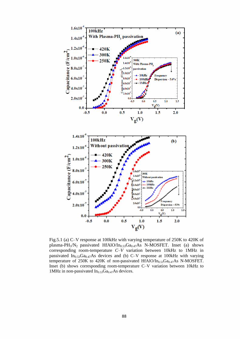
88
Fig.5.1 (a) C–V response at 100kHz with varying temperature of 250K to 420K of
plasma-PH3/N2 passivated HfAlO/In0.53Ga0.47As N-MOSFET. Inset (a) shows
corresponding room-temperature C–V variation between 10kHz to 1MHz in
passivated In0.53Ga0.47As devices and (b) C–V response at 100kHz with varying
temperature of 250K to 420K of non-passivated HfAlO/In0.53Ga0.47As N-MOSFET.
Inset (b) shows corresponding room-temperature C–V variation between 10kHz to
1MHz in non-passivated In0.53Ga0.47As devices.
89
In the mid Eeff region (~0.3 to 0.5MV/cm) of Fig.5.2, µeff of passivated
devices increase with decreasing temperature, implying phonon scattering is
dominant in this region, in particular substrate/bulk phonon scattering. On the
other hand, the temperature dependence of mobility for non-passivated device
is weaker than that of passivated device. This is reasonable because Coulombic
scattering could still play a significant role, such that it partially hides the
effect of phonon scattering or that the weaker temperature dependence of
mobility for non-passivated device may imply dominance of soft optical
phonon scattering (SO) contributed by the HfAlO which has a weak
temperature dependence [13].
In the high Eeff region (~0.6 to 0.7MV/cm), phonon scattering still
persists in passivated device. For non-passivated device, the weak temperature
dependence of mobility suggests the presence of surface roughness scattering
or interface dipole scattering [14]. Similar mechanism has also been reported
from simulation results in Ref [15] where experimental results obtained from
atomic layer deposited Al2O3 on non-passivated In0.53Ga0.47As consists of
Coulombic scattering mechanism dominating at low Eeff and surface roughness
scattering mechanism at high Eeff.

90
Fig.5.2. Effective electron mobility in non-passivated and plasma-PH3/N2
passivated HfAlO/In0.53Ga0.47As N-MOSFET at various temperatures from 250K
to 420K, using the C-V correction method.
5.2.3. Factors Causing Improvement in Mobility of plasma-PH3/N2
Passivated In0.53Ga0.47As MOSFETs 5.2.3.1. Effect of Interface States
In order to understand what contributed to the reduction in Coulombic
scattering in passivated device and hence to explain its higher µeff compared to
non-passivated device in the low to mid-Eeff region, we have investigated the
energy distributions of the Dit shown in Fig.5.3. Dit is strongly reduced in the
upper half of the bandgap for passivated device, due to its ability in reducing
As-As bonds which have their energy states in the upper half of the bandgap
[16-20]. This is expected because based on the plasma-PH3/N2 treatment
mechanism as shown in added Section 2.1.1, hydrogen from the PH3 can
enhance the removal of As element segregation by forming volatile As-H3 that
can be desorbed through evaporation.
91
The lesser amounts of As-As bonds in plasma-PH3/N2 passivated device
relative to non-passivated device can be seen from Table 5.1 which has been
taken from the deconvolution of XPS As3d shown in Fig.5.4 [21]. The
suppression of As-As bonds observed with the use of passivation treatment can
be attributed to the presence of PxNy layer which allows a more bulk-like
In0.53Ga0.47As interface. The existence of this PxNy layer can be evidenced from
the analysis of the XPS peak shifts of N1s and P2p, which matches the XPS
characteristics of P3N5 [22-23]. This suppression of free As is supported by
reported active hydrogen species promoting free As desorption by forming
volatile AsHx species [23]. In addition, the improvement in midgap Dit at
energy levels E-Ei~0.15eV with passivation treatment explains the reduction in
SS, as mentioned in Chapter 4.
The mean Dit for passivated and non-passivated device as shown in
Fig.5.3 is given by 6.02x10¹²
cm-2
eV-1
and 1.24x10¹³
cm-2
eV-1
respectively,
measured from Charge Pumping technique with constant amplitude gate pulse
at frequency of 200kHz and gate pulse amplitude of 1.2V. It is important to
note that fixed charges deduced from the Vfb vs EOT results shown in Fig.5.5
gives values 3.1x10¹¹
cm-2
and 5.1x10¹¹
cm-2
for passivated and non-passivated
device respectively. The density of oxide traps calculated from the C-V
hysteresis for non-passivated (passivated) at 100kHz is given by
8.1x10¹¹
cm-2
(3.4x10¹¹
cm-2
). Since these values of oxide traps and fixed
charges are smaller than Dit, this means that a significant amount of Coulombic
scattering may be attributed to the Dit rather than by fixed charges or the oxide
traps.
Nevertheless, while these results may provide a suggestion as to the
origin of some interface defects responsible for the interface trap density

92
distribution, a definitive statement still cannot be made as to the real
significance of the role of As surface states. This is because the presence of Ga
and In surface states still need to be identified, but due to their smaller binding
energy separation between the peaks, identification of these defect states using
XPS are difficult. Hence more analysis in areas such as electronic spin
resonance would be helpful toward atomic identification of the interface
defects.
In addition, the mean Dit values shown suggest that ideal interface
quality cannot be achieved by simple pre-gate or post-gate treatment alone.
Several groups have shown that with post-gate treatment only, the Dit values of
ALD Al2O3/In0.53Ga0.47As [24-27] are still undesirably high. Hence, further
advances in reducing Dit across the whole bandgap, most likely using both pre-
gate and post-gate treatment, are still required before replacing Si channel by
high indium content InxGa1-xAs. Such methods may include the use of
Fig.5.3. Energy distribution of Dit as determined by the tr and tf dependence of
charge pumping currents. The horizontal lines represent the mean Dit of the entire
bandgap, for non-passivated and plasma-PH3/N2 passivated device.
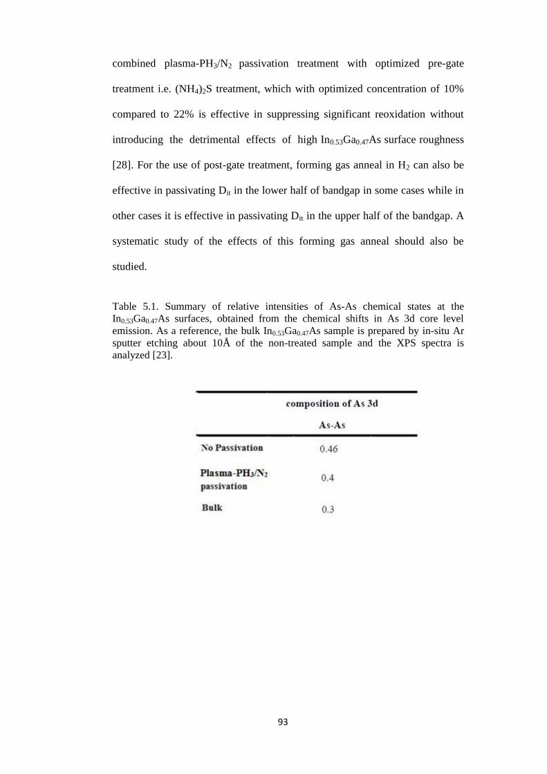
93
combined plasma-PH3/N2 passivation treatment with optimized pre-gate
treatment i.e. (NH4)2S treatment, which with optimized concentration of 10%
compared to 22% is effective in suppressing significant reoxidation without
introducing the detrimental effects of high In0.53Ga0.47As surface roughness
[28]. For the use of post-gate treatment, forming gas anneal in H2 can also be
effective in passivating Dit in the lower half of bandgap in some cases while in
other cases it is effective in passivating Dit in the upper half of the bandgap. A
systematic study of the effects of this forming gas anneal should also be
studied.
Table 5.1. Summary of relative intensities of As-As chemical states at the
In0.53Ga0.47As surfaces, obtained from the chemical shifts in As 3d core level
emission. As a reference, the bulk In0.53Ga0.47As sample is prepared by in-situ Ar
sputter etching about 10Å of the non-treated sample and the XPS spectra is
analyzed [23].

94
Fig.5.4. XPS spectra for the In0.53Ga0.47As surfaces with and without plasma-
PH3/N2 passivation treatment are shown for (a) As 3d. Typical results of
deconvolution analysis are illustrated with the corresponding chemical bonds
indicated [21].
Fig.5.5. Vfb vs EOT plots of passivated and non-passivated In0.53Ga0.47As devices.
Another treatment involved can also be through the use of Fluorine (F)
incorporation into high-k gate dielectric using CF4/O2 plasma treatment. F is
effective in reducing the Dit by 4X at high-k/substrate interface [29]. This is

95
attributed to the termination of oxygen vacancies by the incorporated F atoms
to form stronger Hf-F bonds with higher binding energy. F tends to pile up at
the HfO2/In0.53Ga0.47As interface passivating interface traps, thus resulting in a
better quality interface [29-31]. However, the effect of F incorporation on the
Dit distribution is not investigated yet. One of the disadvantages of plasma-
PH3/N2 passivation technique is the use of plasma which could result in plasma
damage occurring if excessive plasma is applied (such as plasma wattage or
treatment time) as seen in Ref [21]. This plasma damage could result in
disordering, such as dangling bonds and broken bonds, as well as surface
roughening. However, in this work, comparison of the AFM results for sample
after plasma-PH3/N2 passivation treatment shows relatively unchanged values
at 0.15nm compared to 0.16nm for non-passivated sample. This implies that no
plasma damage is observed for this passivation treatment condition. This
shows the importance of optimizing the plasma power and treatment time in
ensuring that plasma damage is minimized.
5.2.3.2. Effect of Phonon Scattering
In addition to Coulombic scattering caused by high densities of Dit,
scattering due to coupling of electrons with the surface optical modes and
substrate longitudinal-optical (LO) phonons, could contribute to the difference
in µeff in both devices [32]. Fig.5.6 shows the µeff, mobility limited by
Coulombic scattering, µcoul, mobility limited by phonon scattering, µph,
and mobility limited by surface roughness scattering, µsr, as a function of
Eeff at 300K for N-MOSFETs with and without passivation. To obtain the µph
values, we made use of the Mathiessen‘s rule: 1/µph = 1/µeff -1/µcoul -1/µsr.,
where µcoul is extracted from the µeff at low fields by linear fitting and
96
extrapolated to high Eeff,. This dependency is linear due to the increasing
carrier screening effects of the electrons with increase in electric field, which
causes the attractive potential of the electrons with the charged centers to
weaken. In order to obtain µsr, it is best to measure the device at temperatures
as low as 77K in order to limit the contribution of phonon scattering to the µeff.
However, we were unable to perform such measurements due to the lack of
resources.
Hence µsr plotted in Fig.5.6 is obtained from the simulated µsr results of
HfO2/In0.53Ga0.47As device with p-type doping concentration of 3x10¹⁷
cm-3
taken from Ref [32]. The µsr have been obtained from Ando’s model, with an
exponential correlation spectrum, as well as degenerate-static-multisubband
screening included.
The µsr simulated [32] is given by RMS asperity height (Δ) ~0.48nm
and correlation length (λ) ~1.2nm. AFM measurements reveal that Δ for our
device is given by ~0.15nm and ~0.16nm for passivated and non-passivated
device respectively, for devices without 600C S/D anneal. However since the
step height for non-passivated device seen from TEM image taken with 600C
S/D anneal in Fig.4.5(a) is small/insignificant and this occurs only in localized
regions, we can assume that Δ is still almost the same as without S/D anneal.
Hence using the µsr obtained from simulation to assume the lower limit for the
expected µsr is reliable.
Similarly for passivated device, the TEM step height seen in Fig.4.5(b)
is negligible and hence no significant deviation from RMS height obtained
from AFM for without S/D anneal is expected. Thus, given that the RMS
height is similar for both non-passivated and passivated devices, the use of the
same µsr values to extract µph of both devices is reliable since the expected

97
increase in µsr for passivated device compared to non-passivated is only 1.14X
due to µsr being proportional to /2
[33].
µsr starts to become a significant factor at Eeff > 0.7MV/cm from
Fig.5.6 but this value of Eeff where µsr starts to play a significant role depends
on the exponent of Eeff. The exponent of Eeff is dependent on the value of
[34]. Following the approach that was used in Ref [33], we also assumed that
is the same for both non-passivated and passivated devices and hence the
exponent of Eeff would be the same [33]. Thus, the µsr would only become a
significant factor at high Eeff of 0.7MV/cm for both non-passivated and
passivated devices which is not within the region where µph is extracted from.
This means the µph extraction is reliable.
Fig.5.6. µeff, µcoul, µph, µsr, for passivated and non-passivated device obtained using
Matthiessen‘s rule.
Fig.5.6 shows that the mobility limited by phonon scattering for the
non-passivated device is significantly lower than the passivated device,

98
indicating a more severe phonon scattering for the non-passivated device.
Assuming no significant difference in bulk In0.53Ga0.47As of both non-
passivated and passivated device, the phonon scattering contribution from the
substrate is expected to be similar for both samples. Thus, this suggests that the
reason for the additional source of phonon scattering in non-passivated device
could be due to the effects from HfAlO gate dielectric. To investigate the
reason for this source of additional phonon scattering, we studied the phonon
scattering rate as a function of temperature as shown in Fig.5.7. Phonon
scattering rate is taken from the equation (q/(µm*)) [13], where m* is the
effective mass of the carrier in In0.53Ga0.47As inversion channel taken as
0.041mo with mo as the free electron mass. By taking the difference between
the two sets of phonon scattering rate curves in Fig.5.7, we can get the
scattering rate caused by this additional phonon source in the HfAlO of the
non-passivated device, and this curve is also plotted in Fig.5.7. From the two
dimensional deformation potential theory of surface phonon scattering, the
scattering rate due to optical phonon may be expressed as [13,35] Equation
(5.4):
1/ op [NR (NR 1) u(E ℏ)]
where NR = (1/(e ℏ/kT
–1)) is the phonon occupation number, E is the carrier
energy, is the phonon frequency, and u(x) is the unit step function,
u(x < 0)=0 and u(x > 0)=1. Assuming that the phonon energy is smaller than
thermal carrier energy i.e. ℏ < E, then Equation (5.5) shows that:
1/ op (2NR 1) ((eχ +1)/(e
χ -1)) where χ=ℏ/kT
Equation (5.5) indicates that when ℏ << kT, (1/op) T, and when
Equation (5.4)
Equation (5.5)

99
ℏ > kT, (1/op) approaches a constant i.e. independent of temperature [13]. In
order to investigate the characteristics of the phonon scattering contributed by
the high-k, its two transverse optical (TO) phonons with energies ℏ would be
used. For HfAlO, the values of TO1 and TO2 for HfAlO are assumed to be
those between HfO2 and Al2O3. TO1 for HfO2 is given as 12.40meV and its
TO2 is 48.35meV, while TO1 for Al2O3 is given as 48.18meV and its TO2 is
71.4meV [36]. Comparison of the above values with kT of 21.5meV-
36meV (for our measurement temperatures of 250K to 420K), a temperature
independent scattering rate for TO2 phonons is expected since ℏ> kT where
ℏis between 48.35meV to 71.4meV and kT is 21.5meV-36meV. On the
other hand, TO1 phonons scattering rate can have a linear temperature
dependence if ℏ< 36meV, where ℏis between 12.4meV to 48.18meV. It
can also have a temperature independent scattering rate if ℏ > 21.5meV.
Thus, from the results where a temperature independent scattering rate for the
TO2 phonons, and a temperature independent to linear temperature dependence
for the TO1 phonons is observed, this explains the weak temperature
dependence of the scattering rate of non-passivated device seen in Fig.5.7.
Weak temperature dependence is a characteristic of SO phonon
scattering, in contrast to phonon scattering contributed by the bulk phonons
from the substrate which has stronger temperature dependence [13]. This
implies the reason for the additional source of phonon scattering rate in non-
passivated device is due to the HfAlO.
The reason for this is likely due to the thinner interfacial layer thickness
given by ~0.35nm for the non-passivated device, while it is given by ~0.6nm
for the passivated device, as deduced from the intercept of the EOT vs physical
oxide thickness in Fig.4.7. Even though the difference in interfacial layer

100
thickness is small, based on high-k/SiO2/Si system, even a slight increment
(~0.1nm) in SiO2 interfacial layer thickness can result in an exponential
improvement in μph [37-38]. This is based on the physical mechanism where
the scattering amplitude matrix element decreases away from the dielectric
interface as e-Qt
, where Q represents the in-plane momentum transfer and t is
the distance from the interface [37]. Thus, this SiO2 interfacial layer between
the channel and the HfO2 reduces the detrimental effect of the soft optical
phonon scattering on the mobility through decoupling between the motion of
electrons in the inversion layer and those SO phonons in the high-k dielectric.
Therefore, similar methodology or reason can be applied to our high-
k/In0.53Ga0.47As system where a ~0.25nm smaller interfacial layer thickness
than the passivation layer of PxNy can result in the significant reduction to μph
of non-passivated device, contributed by the significant SO phonon scattering
in the HfAlO.
Fig.5.7. Phonon scattering rate vs Temperature for passivated and non-passivated
devices, with difference between both phonon scattering rates being contributed by
the SO phonon scattering caused by HfAlO in the non-passivated device.

101
5.2.3.3. Effect of Interface Dipole Scattering
It is seen that the temperature dependences of µeff in the non-passivated
device in the high Eeff regime is weak (from Fig.5.2). Based on the TEM image
in Fig.4.5(a), non-uniform interfacial layer with unclear high-k/In0.53Ga0.47As
interface and some non-uniform transition regions is observed while clear
transitions and atomically sharp and smooth interface between HfAlO and
In0.53Ga0.47As can be observed for passivated device in Fig.4.5(b). Thus the
possibility of surface roughness scattering as one of the causes of weak
temperature dependence of mobility for non-passivated device cannot be
ignored. However, this effect may not be significant due to localized areas of
the non-passivated device where the step height is higher than passivated
device.
Nevertheless, the correlation between the mobility at high E-field and
shift in Vfb in the negative direction (given by difference between y-axis
intercept and Vfb ideal of Fig.5.5 which corresponds to the dipole strength)
shows there is another mechanism that possibly contributes to the weak
temperature dependence of the non-passivated device at high E-field. It is seen
that with stronger interface dipole strength, µeff increases. The stronger
interface dipole strength observed in passivated device could be due to the
ordering of the interface dipoles i.e. more ideally aligned dipoles contributing
to smaller interface dipole scattering. On the other hand, non-passivated device
experience smaller interface dipole strength possibly caused by randomly
oriented dipoles which scatter the carriers i.e. more interface dipole scattering.
This can occur due to the interdiffusion of elements of high-k and
102
In0.53Ga0.47As substrate across the interface which induces dipole fluctuation,
thus contributing to carrier scattering which results in lower µeff [39-40].
Fig.5.8 shows the Ga 3d and In 4d XPS spectra obtained from 2nm
HfAlO deposited on In0.53Ga0.47As at take-off angle (TOA) of 30° and 90° for
both passivated and non-passivated devices with and without PDA. P1/P2 ratio
from Fig.5.9 shows the deconvoluted area ratio of the peaks present in the
Ga3d and In4d spectra taken from Fig.5.8. P1 (spectra at ~19eV) includes the
area of Hf4f5/2 and Ga3d peaks while P2 (spectra at ~17eV) includes the area at
Hf4f7/2 and In4d peaks. Fig.5.9 depicts that non-passivated device has a larger
change in Ga/In ratio than passivated device.
Obtaining accurate values of Ga/In ratio is difficult due to the XPS
lines of Ga and In being strongly overlapped with Hf. Therefore, we are
comparing the change in P1/P2 ratio (comparing P1/P2 ratio for conditions
without and with PDA), to deduce that there is larger intermixing/interdiffusion
of Ga/In near the high-k/In0.53Ga0.47As interface for non-passivated device,
which may be responsible for the existence of larger amounts of randomly
oriented dipoles in non-passivated device.

103
Fig.5.8. Ga 3d and In 4d (a) XPS spectra for the In0.53Ga0.47As surfaces without
and (b) with plasma-PH3/N2 passivation treatment are shown.
Change in P1/P2 ratio can be correlated with change in Ga/In ratio
since the ideal ratio of Hf4f5/2/Hf4f7/2 is found to be ¾, and is not expected to
change regardless of the thickness and the measurement condition. Passivated
device shows smaller change in P1/P2 ratio, which implies that the passivated
device is more robust to interdiffusion of Ga/In elements across the high-
k/In0.53Ga0.47As interface.
Plasma-PH3/N2 passivation results in reduced amount of interdiffusion
of elements within the HfAlO/In0.53Ga0.47Asinterface and hence effective in
reducing the degree of interface dipole scattering. This is because of the
formation of a thin PxNy passivating layer over the P terminated surface,
caused by P-for-As reaction, before high-k deposition. This PxNy interlayer has
strong mechanical properties and is a chemically and thermodynamically stable
material, with the presence of stable and strong covalent bond due to its cross-
linked structure [41-42]. In addition, the presence of P-for-As exchange
reaction, which is also present in our plasma-PH3/N2 passivation treatment
process, causes Ga-P bond to be present in passivated device [23], which is

104
stronger than that of Ga-As bond, due to its larger heat of formation. Hence,
the chances of breaking the Ga-P bonds, to result in interdiffusion of elements
across the interface, at high temperature processing (for instance during PDA
or S/D activation annealing) would be reduced in the passivated device.
However, too excessive In/Ga-P bond formation may result in formation of
artifacts that can further worsen device performance [23].
Hence, as seen from the chemical analysis from XPS data, it is believed
that the small amount of crystalline disorders/defects present in the substrate of
the non-passivated device below the HfAlO/In0.53Ga0.47As interface as shown
in the highlighted box of the high resolution-TEM (HR-TEM) image as seen in
Fig.4.5(a) could possibly be due to the effects of the interdiffusion of the
high-k and In0.53Ga0.47As elements [39-40]. Such defects are not obvious from
the HR-TEM image of the passivated device seen in Fig.4.5(b). Nevertheless, it
is important to note that surface roughness scattering may also play a part in
Fig.5.9. XPS analysis showing P1/P2 ratio as a function of conditions (with and
without PDA) applied to the samples. The P1/P2 ratio has been taken from the
deconvolution of the peaks from XPS Ga 3d and In 4d of Fig 5.8.

105
this regime due to the HR-TEM image seen in Fig.4.5(a) which reveals a slight
waviness at the high-k/In0.53Ga0.47As interface for non-passivated device,
suggesting that its poorer interface roughness could also be responsible for the
lower µeff observed.
5.3. Conclusion
As a conclusion, this chapter investigated the inversion layer scattering
mechanisms of HfAlO/In0.53Ga0.47As N-MOSFETs with plasma-PH3/N2
passivation layer to understand the physical origins of mobility enhancement
compared to non-passivated device. The mobility extraction technique used for
interface trap correction used for this work has been discussed in Section 5.2.1
and followed by the evaluation of a temperature dependence study of the
mobility on the mobility degradation mechanisms present in plasma-PH3/N2
passivated In0.53Ga0.47As MOSFETs as well as non-passivated MOSFETs in
Section 5.2.2. Section 5.2.3 investigated the physical origins of mobility
enhancement of HfAlO/In0.53Ga0.47As N-MOSFETs with plasma-PH3/N2
passivation layer. It is found that the mobility enhancement of plasma-PH3/N2
passivated device is caused by the reduction in Coulombic scattering caused by
the reduced As-As bond formation, as well reduced soft optical phonon
scattering associated with reduced interactions of the surface optical phonons
in the high-k oxide. In the high Eeff, the reduction in the interface dipole
scattering is caused by the decrease in the interdiffusion of elements from
HfAlO and In0.53Ga0.47As substrate, which prevents formation of randomly
oriented dipoles.

106
REFERENCES
[1]S. Koveshnikov, W. Tsai, I. Ok, J.C. Lee, V. Torkanov, M. Yakimov, and S.
Oktyabrsky, “MOSCAP on GaAs with high-k gate oxide and amorphous silicon
interface passivation layer”, Appl. Phys. Lett., Vol. 88, pp. 22106(1)-22106(3), 2006.
[2]Y. Sun, E.W. Kiewra, J.P. de Souza, J.J. Bucchignano, K.E. Fogel, D.K. Sadana
and G. G. Shahidi, “High-Performance In0.7Ga0.3As-Channel MOSFETs With High-
Gate Dielectrics and -Si Passivation”, IEEE Electron Device Lett., Vol. 30, pp. 5-
7, 2009.
[3]D. Shahrjerdi, E. Tutuc and S. K. Banerjee, “Impact of surface chemical treatment
on capacitance-voltage characteristics of GaAs metal-oxide-semiconductor capacitors
with Al2O3 gate dielectric”, Appl. Phys. Lett., Vol. 91, pp. 063501(1)-063501(3),
2007.
[4]H.J. Oh, S.A.B. Suleiman, G.Q. Lo, D.L. Kwong, D.Z. Chi and S. Lee, “Thermally
Robust Phosphorous Nitride Interface Passivation for InGaAs Self-Aligned Gate-First
N-MOSFET Integrated with high-k Dielectric”, Tech. Dig. – Int. Electron Devices
Meet., pp.339-342, 2009.
[5]S. Takagi, A. Toriumi, M. Iwase, and H. Tango. “On the universality in Si MOS-
FETs: Part I - effects of substrate impurity concentration”, IEEE Trans. Elec. Dev.,
Vol.41, pp.2357-2362, 1994.
[6]S. Takagi, A. Toriumi, M. Iwase and H. Tango, “On the Universality of Inversion
Layer Mobility in Si MOSFET's: Part I-Effects of Substrate Impurity Concentration”,
IEEE Trans. Ele. Dev., Vol.41, No.12, pp. 2357, 1994.
[7]W. Zhu, J.P. Han, and T.P. Ma. “Mobility measurement and degradation
mechanisms of MOSFETs made with ultrathin high-k dielectrics”, IEEE Trans. Elec.
Dev., Vol.51, pp.98-105, 2004.
[8]K. Martens, “Electrical characterization and Modeling of Ge/III-V- Dielectric
Interfaces”, PhD Dissertation, IMEC, 2009.
[9]A. Ali, H. Madan, S. Koveshnikov and S. Datta, “Small Signal Response of
Inversion Layers in High Mobility In0.53Ga0.47As MOSFETs Made with Thin high-k
Dielectrics”, IEEE Trans. Elec. Dev., Vol. 57, pp. 742-748, 2010.
[10]D.K. Schroder, "Semiconductor Material and Device Characterization", John
Wiley & Sons, 1998.
[11]C.L. Hinkle, A.M. Sonnet, R.A. Chapman, and E.M. Vogel, “Extraction of the
Effective Mobility of In0.53Ga0.47As MOSFETs”, IEEE Ele. Dev. Lett., Vol. 30, No. 4,
pp.316, 2009.
[12]H. Hasegawa and T. Sawada, “Electrical Modeling of Compound
Semiconductor Interface for FET Device Assessment”, IEEE Trans. Ele. Dev., Vol.27,
pp.1055, 1980.
[13]W.J. Zhu, and T.P. Ma, “Temperature dependence of Channel Mobility in HfO2-
Gated MOSFET”, IEEE Ele. Dev. Lett., Vol. 25, pp. 89-91, 2004.

107
[14]Y. Urabe, N. Miyata, H. Ishii, T. Itatani, T. Maeda, T. Yasuda, H. Yamada, N.
Fukuhara, M. Hata, M. Yokoyama, N. Taoka, M. Takenaka, S. Takagi, “Correlation
between Channel Mobility Improvements and Negative Vth Shifts in III-V MISFETs:
Dipole Fluctuation as New Scattering Mechanism”, Tech. Dig. – Int. Electron Devices
Meet., pp. 142-145, 2010.
[15]T.P. O‘Regan, M.V. Fischetti, B. Soree, S. Jin, W. Magnus and M. Meuris,
“Calculation of the electron mobility in III-V inversion layers high-κ dielectrics”, J.
Appl.Phys., Vol. 108, pp. 103705, 2010.
[16]G. Brammertz , H. C. Lin, K. Martens, D. Mercier, C.Merckling, J. Penaud, C.
Adelmann, S. Sioncke, W. E. Wang, M. Caymax, M. Meuris, and M. Heyn,
“Capacitance–Voltage Characterization of GaAs–Oxide Interfaces”,
J.Electrochem.Soc, Vol.155, pp. H945-H950, 2008.
[17]J. Robertson“Interface states model for III-V oxide interfaces”,Microelectronic
Eng., Vol.86, pp. 1558-1560, 2009.
[18]H.P. Komsa and A. Pasquarello “Identification of defect levels at InxGa1
xAs/oxide interfaces through hybrid functionals”, Microelectronic Eng., Vol.88,
pp.1436-1439, 2011.
[19]J. Robertson, “Model of interface states at III-V oxide interfaces”, Appl.Phys.Lett.
Vol.94, pp.152104, 2009
[20]L. Lin, J. Roberston, “Defect states at III-V semiconductor oxide interfaces”,
Appl.Phys.Lett., Vol.98, pp.082903, 2011.
[21]Oh Hoon Jung, “Development of High mobility channel layer formation
technology for high speed CMOS Devices”, PhD dissertation, National University of
Singapore, 2010
[22]H.J. Oh, S.A.B. Suleiman, G.Q. Lo, D.L. Kwong, D.Z. Chi, and S. Lee,
“Thermally robust phosphorous nitride interface passivation for InGaAs self-aligned
gate-first N-MOSFET integrated with high-k dielectric”, Tech. Dig. – Int. Electron
Devices Meet., pp. 339–342, 2009.
[23]H.J. Oh, Sumarlina A.B.S and S.J. Lee, “Interface Engineering for InGaAs N-
MOSFET Application Using Plasma PH3–N2 Passivation”, J. Electrochem. Soc.,Vol.
157, pp. H1051-H1060, Sep. 2010.
[24]G. Brammertz, H. C. Lin, K. Martens, A. Alian, C. Merckling, J. Penaud, D.
Kohen, W.-E Wang, S. Sioncke, A. Delabie, M. Meuris, M. Caymax, and M. Heyns,
“Electrical Properties of III-V/oxide interfaces”, Electrical Chemical Society spring
meetings, pp. 375–38, 2009.
[25]H.C. Lin, W.E. Wang, G. Brammertz, M. Meuris, and M. Heyns, “Inversion
behavior on n and p type ALD— Al2O3 / In0.53Ga0.437As MOS capacitors”, IEEE
Semiconductor Interface Specialists Conference, 2008.
[26]H.C. Lin, G. Brammertz , K. Martens, G. de Valicourt, L. Negre, W.-E Wang,
W.Tsai, M. Meuris, and M. Heyns, “Application of Fermi Level Efficiency Method to
the analysis of high interface trap density oxide-semiconductor interfaces”,
App.Phys.Lett., Vol.94, pp.153508, 2009.
108
[27]Y. Xuan, Y.Q. Wu, and P.D. Ye, “High-performance inversion-type
enhancement-mode InGaAs MOSFET with maximum drain current exceeding 1
A/mm”, IEEE Ele.Dev.Lett., Vol.29, pp.294–296, 2008.
[28]É.O Connor, B. Brennan, V. Djara, K. Cherkaoui, S. Monaghan, S.B. Newcomb,
R. Contreras, M. Milojevic, G. Hughes, M.E. Pemble, R.M. Wallace, and P.K. Hurley
, “A systematic study of (NH4) 2S passivation 22%, 10%, 5%, or 1%,on the interface
properties of the Al2O3/In53Ga0.47As/InP system for n-type and p-type In53Ga0.47As
epitaxial layers”, J.Appl.Phys., Vol.109,pp. 024101, 2011
[29]Y.T. Chen, Y. Wang, F. Xue, F. Zhou and J.C. Lee, “Optimization of Fluorine
Plasma Treatment for Interface Improvement on HfO2/In0.53Ga0.47As MOSFETs”,
App.Sci., Vol.2, pp.233, 2012.
[30]Y. Chen, H. Zhao, J.H. Yum, Y. Wan and F. Xue, “Improved electrical
characteristics of TaN/Al2O3/In0.53Ga0.47As metal oxide-semiconductor field-effect
transistors by fluorine incorporation”, App. Phys. Lett., Vol.95,pp. 013501, 2009.
[31]H.C. Chin, X. Gong, L.Wang and Y.C. Yeo, “Fluorine Incorporation in HfAlO
Gate Dielectric for Defect”, Electrochem. Solid-State Lett., Vol. 13, pp. H440-H442,
2010.
[32]T. P. O‘Regan, M.V. Fischetti, B. Soree, S. Jin, W. Magnus, and M. Meuris,
“Calculation of the electron mobility in III-V inversion layers high-κ dielectrics”, J.
Appl. Phys., Vol. 108, pp. 103705, 2010.
[33]W.Weike, “Analysis of Electron Mobility in Inversion-Mode Al2O3/InxGa1−xAs
MOSFETs”, IEEE Trans.Ele.Dev,Vol.58, pp.1972, 2011.
[34]G.Mazzoni, A.L.Lacaita, L.M.Perron and A.Pirovano, “On Surface Roughness-
Limited Mobility in Highly Doped n-MOSFET’s”, IEEE Trans.Ele.Dev, Vol.46,
p.1423, 1999.
[35]C.T. Sah, T.H. Ning, and L.L. Tschopp, “The scattering of electrons by surface
oxide charges and by lattice vibrations at the silicon-silicon dioxide interface”, Surf.
Sci.,Vol.32, pp. 561-575, 1972.
[36]M. Fischetti, D. Neumayer and E. Carttier, “Effective electron mobility in Si
inversion layers in metal–oxide–semiconductor systems with a high-k insulator: The
role of remote phonon scattering”, J. Appl.Phys., Vol. 90, pp. 4587, 2001.
[37]J.R. Watling A.R. Brown, G. Ferrari, J.R. Barker, G. Bersuker, P. Zeitzoff, and A.
Asenov, “Impact of high-k Gate Stacks on Transport and Variability in Nano-CMOS
Devices”, J. Comp. Theor. Nanosci., Vol. 5, pp. 1072-1088, 2008.
[38]R. Shah, and M.M. De Souza, “Impact of a Nonideal Metal Gate on Surface
Optical Phonon-Limited Mobility in High-κ Gated MOSFETs”, IEEE Trans. Elec.
Dev., Vol. 54, No. 11, pp. 2991-2997, 2007.
[39]E.J. Kim, E. Chagarov, J. Cagnon, Y. Yuan, A.C. Kummel, P.M. Asbeck, S.
Stemmer, K. C. Saraswat, and P.C. McIntyre, “Atomically abrupt and unpinned
Al2O3/ In0.53Ga0.47As interfaces: Experiment and simulation”, J. Appl.Phys., Vol. 106,
pp.124508, 2009.
[40]L. Lin and J. Robertson, “Atomic mechanism of electric dipole formed at high-k:
SiO2 interface”, J. Appl.Phys., Vol. 109, pp. 094502, 2011.

109
[41]W. Schnick, J. Lücke and F. Krumeich, “Phosphorus Nitride P3N5: Synthesis,
Spectroscopic and Electron Microscopic Investigations”, Chem. Mater., Vol.8,pp.281-
286,1996.
[42]G. Sproul, “Electronegativity and bond type. Evaluation of electronegativity
scales”, J. Phys. Chem., Vol. 98, pp. 6699-6703, 1994.
110
Chapter 6: TCAD Simulation of Non-passivated and
plasma-PH3/N2 Passivated In0.53Ga0.47As MOSFET for
Scalability Evaluation
6.1. Introduction and Motivation
The goal of this chapter is to evaluate effectiveness of plasma-PH3/N2
passivation in achieving and improving scalability in In0.53Ga0.47As MOSFETs
through TCAD simulations. For realistic study on this aspect, TCAD
simulation model parameters must be tuned so that they are able to predict
measured data of reported devices reasonably accurately. Hence it is important
to identify a good measurement results set that can be used for model
parameter tuning purpose. The device performance of the fabricated sub-
100nm plasma-PH3/N2 HfAlO/In0.53Ga0.47As MOSFETs fabricated in this work
has high contact resistance and increased gate to source-drain spacing
compared to another lot fabricated in our group, and hence these data are not
best suited to calibrate model parameters. Hence, the device model calibration
parameters and optimization for scalability studies in this thesis has been based
on our group’s IEDM 2008 long channel (4µm) non-passivated and plasma-
PH3/N2 passivated HfO2/In0.53Ga0.47As MOSFETs as well as the short channel
(95nm) plasma-PH3/N2 passivated HfO2 In0.53Ga0.47As MOSFET electrical data
performance. The device models and the parameters used for calibration to fit
the electrical data from the long channel and short channel gate length
MOSFETs will be described in Section 6.2. This section will also explore,
based on the energy diagram, the effect of Dit at different energy trap location
on the Id-Vg results. In addition, through simulation, it can be further confirmed
that the smaller Vth and SS of plasma-PH3/N2 passivated device is caused by

111
the smaller concentration of acceptor-like traps while its smaller Ioff and SS is
due to its smaller concentration of donor-like traps as also mentioned in
Chapter 4. Using the same device calibration model parameters, Section 6.3
shows the expected performance scalability of non-passivated vs plasma-
PH3/N2 passivated In0.53Ga0.47As MOSFETs using the existing process flow.
6.2. Calibration of Simulation Parameters for 95nm Gate Length
Fabricated In0.53Ga0.47As MOSFET with Implanted S/D
The experimental data for fitting simulation parameters to realistic
values has been taken from the 4µm and 95nm gate length TaN/ 10nm HfO2/
1x10¹⁷
cm-3
p-type In0.53Ga0.47As/ 1x10¹⁸
cm-3
p-type InP buffer/ 3x10¹⁸
cm-3
p-
type substrate MOS devices [1]. Two types of 4µm devices i.e. one with
plasma-PH3/N2 passivation and another one without plasma-PH3/N2
passivation, have been used for the calibration purposes. Good match between
the simulated and the experimental device characteristics have been obtained
by calibrating the simulation parameters as seen in Fig.6.1. The simulations
have been performed using 2D device simulator, MEDICI [2].
First step involved in the fitting of the 4µm non-passivated and
passivated device characteristics to the experimental device characteristics is
by varying the TaN gate work function between 4.44eV to 4.53eV in order to
fit the Vth. Next step is performing a curve fit focused on the subthreshold
region by varying the Dit distribution as well as the HfO2 dielectric constant.
The fitting of the Id-Vg curves for both devices have been pursued by adopting
the Dit distributions as shown in Fig.6.2, which is in agreement with the
interface trap distribution of HfO2/In0.53Ga0.47As MOSFET reported in [3]. The
acceptor-like traps exist at energy levels above the CNL, while donor-like traps
112
exist at energy levels below the CNL. CNL in Fig.6.2 is at 0.24eV above
intrinsic Fermi level (Ei), a value chosen which is between 0.104eV above Ei
[4] and also within Ec [5] reported in literature. HfO2 permittivity values of 13
for passivated device and 12 for non-passivated device has been used,
based on the EOT values given as 3nm and 3.2nm respectively taken from the
published C-V results [1], for which I-V data is shown in Figs.6.1(a)-(b).
Next step involved the fitting of the linear and saturation region currents
of the long channel devices. Mobility models used include Lombardi‘s model
for low lateral field mobility and high-k mobility model (both to model the
mobility degradation at semiconductor-insulator interface due to perpendicular
field and remote phonon scattering prevalent with use of high-k dielectrics) and
the high lateral field GaAs like mobility model with velocity overshoot. These
models were used to reproduce the inversion mobility measured using the split
C-V method. Different mobility input parameters for low field mobility model,
but same high field mobility model input parameters, were used for 4µm non-
passivated and plasma-PH3/N2 passivated devices. The values used for
bandgap and electron affinity have been based on literature which determines
the band alignment [6-7]. In addition, band-to-band tunnelling and quantum
mechanical models were included. Three valley band related models were
turned on in order to capture the effects of intervalley transfer by varying the
electron effective mass at different satellite states which will impact the drive
current. This is important especially at high lateral fields where the possibility
of electron transfer to the upper satellite valley will be higher.

113
Fig.6.1 (a) Comparison between the experimental and simulated Id-Vg
characteristics of 4µm gate length non-passivated In0.53Ga0.47As MOSFET and (b)
Comparison between the experimental and simulated Id-Vg characteristics of 4µm
gate length plasma-PH3/N2 In0.53Ga0.47As MOSFET.
The S/D doping has been modelled by Gaussian profiles with adjustments
to reproduce the S/D sheet resistance taken from the reported transmission line
method (TLM) measurement as 80Ω/sq with junction depth given by 100nm
[8]. The peak carrier concentration 3.5x10¹⁸
cm-3
located at the surface of
semiconductor is used, which is similar to the experimental peak carrier
(b)

114
concentration obtained with the similar implant and annealing conditions given
by 2.3x10¹⁸
cm-3
[9]. The contact resistance 600Ω.µm of the long channel
devices is taken from the reported TLM measurements [8]. The TCAD
calibration parameters including the band alignment parameters have been
included in Table 6.1. The simulation results with calibrated model parameters
for the 4µm non-passivated and passivated devices to the experimental results
are shown in Fig.6.1(a) and Fig.6.1(b) respectively. This set of parameters is
sufficiently accurate for predicting Ion, Ioff, DIBL and SS which are vital for
device performance evaluation for scalability.
Table 6.1. Parameters used in the calibration of the device models.
For the calibration of the simulation parameters of the short channel
(95nm Lg) non-passivated device, similar mobility model input parameters, as
well as other model parameters, to the 4µm non-passivated device have been
used. The only difference is in terms of the higher work function used at
4.81eV, S/D peak doping concentration at 5.5x10¹⁸
cm-3
, junction depth of
32nm due to different implant conditions at 20keV/1x1014
cm-2
resulting in
matched measured sheet resistance of ~250Ω/sq [10]. The S/D contact to gate
has a spacing of 2µm, with contact resistances set at 1200Ω.µm reported from
TLM measurements [8]. The results are shown in Fig.6.3. Id,sat and
subthreshold region of the non-passivated device is fitted well except the on-

115
state current at low Vd. This set of parameters is sufficiently accurate for
predicting Ion, Ioff , DIBL and SS which are vital for device performance
evaluation for scalability. We also show the predicted performance
enhancement, using the same Dit distribution and mobility input parameters for
low field and high field obtained from the long channel 4µm plasma-PH3/N2
passivated device, for the plasma-PH3/N2 passivated 95nm Lg device. Similar
to the long channel device, the expected Id-Vg for passivated device also shows
Vth shifted to the left and reduced DIBL caused by lesser amount of interface
traps. The DIBL is given by 100mV/V for the predicted plasma-PH3/N2
passivated device while non-passivated device has DIBL 127mV/V. The SS for
plasma-PH3/N2 passivated device is 169mV/dec compared to 233mV/dec for
non-passivated device at Vd=1V, corresponding to the increasing contribution
of the SCE to the SS and DIBL of the 95nm Lg device. Id,sat is given by
273µA/µm for plasma-PH3/N2 passivated device, which is more than 2X
increase compared to the Id,sat of non-passivated device at 120µA/µm. This is
attributed to the larger mobility caused by reduced interface scattering at the
HfAlO/In0.53Ga0.47As interface.

116
Fig.6.2. Dit distribution, with trap energy level with respect to the intrinsic Fermi
level, of HfO2/In0.53Ga0.47As MOSFET with and without plasma-PH3/N2
passivation simulated for Id-Vg fitting. Only the upper half of the bandgap is
shown for fitting since the simulation results for surface channel architecture
MOSFETs are sensitive to this part of the bandgap only [11]. Note that traps
above the CNL are defined as acceptor-like traps while traps below this level are
defined as donor-like traps.
Fig.6.3. Calibration of non-passivated Lg=95nm with 10nm thick HfO2 device
showing matching to the experimental results. Expected performance enhancement
prediction through plasma-PH3/N2 passivation using simulation is also shown.

117
6.3. Effect of Interface Trap Density on Threshold Voltage of Non-
passivated and plasma-PH3/N2 Passivated MOSFET
As mentioned in Chapter 4, the smaller concentration of acceptor-like
traps for plasma-PH3/N2 device was identified to be responsible for reduced
Vth. The Dit distribution used in the simulations as a function of energy from
the intrinsic Fermi level Ei is concentrated in the upper half of the bandgap as
seen in Fig.6.2, due to its surface channel architecture [11]. Note that Ei has
been calculated as 0.416eV based on standard Equation (6.1):
It will be shown here which Dit energy location corresponds to which point of
the Id-Vg curves taken from Figs.6.1(a)-(b). Looking at Fig.6.4(a) and
Fig.6.4(b), taken at Vg=-0.5V and Vd=0.05V which corresponds to the off-state
of non-passivated and plasma-PH3/N2 passivated device shown in Fig.6.1(a)
and Fig.6.1(b) respectively, non-passivated device has EF at 0.17eV below Ec
while passivated device has EF at 0.22eV below Ec. Thus Vg for non-passivated
device will sweep at 0.154eV above Ei. Since Ec energy level with respect to
Ev is given as 0.74eV and Ei energy level with respect to Ev is given as
0.416eV, EF at 0.17eV below Ec corresponds to energy level of 0.57eV with
respect to Ev. Hence, 0.57eV-0.416eV=0.154eV would mean EF is 0.154eV
above Ei at off-state. Similarly, passivated device will sweep at 0.104eV above
Ei. At these two locations, which are given by 0.154eV and 0.104eV above Ei
for non-passivated and plasma-PH3/N2 passivated device respectively, the
density of donor-like traps is higher for non-passivated compared to passivated
device as seen from Fig.6.2 Dit distribution. Hence, this explains the larger
subthreshold slope and leakage for non-passivated than passivated case as seen
Equation (6.1)

118
from Fig.6.1(a) and Fig.6.1(b) at Vg=-0.5V, Vd=0.05V.
As Id from Fig.6.1(a) and Fig.6.1(b) continues to increase to 0.1µA/µm,
EF will sweep through much smaller range on magnitude of Dit. Before
achieving strong inversion, Fig.6.5(a) below shows EF at 0.059eV away from
Ec for non-passivated device and 0.0988 away from Ec for passivated device.
This corresponds to 0.265eV away from Ei for non-passivated device and
0.225eV away from Ei for passivated device, based on similar calculations
mentioned earlier. The fact that energy level is currently at 0.265eV away from
Ei for non-passivated device, this means it is beyond the CNL. Hence,
acceptor-like traps residing at this energy level for non-passivated device
would start to play a part in affecting device performance, while plasma-
PH3/N2 treated device which has energy level at 0.225eV away from Ei still has
donor-like traps controlling the device performance. Thus the acceptor-like
traps given by trap concentration of ~2x10¹³
cm-2
eV-1
at energy level of
0.265eV seen in Fig.6.2 would contribute to a positive shift in Vg to the right at
Id=0.1µA/µm in Fig.6.1(a) for non-passivated device. On the other hand, the
donor-like traps given by trap concentration of ~5x10¹²
cm-2
eV-1
at energy level
of 0.225eV away from Ei for passivated device seen in Fig.6.2 would
contribute to Vg shift to the left at Id=0.1µA/µm in Fig.6.1(b). This explains the
Vg shift to the right to Vg=-0.036V for non-passivated and Vg shift to the left to
Vg=-0.2V for passivated device, when taken at Id =0.1µA/µm.
119
The energy band diagram for the respective threshold voltage states
taken at 0.5µA/µm from Fig.6.1(a) and Fig.6.1(b), which corresponds to
Vg=Vth=0.1V for non-passivated and Vg=Vth=-0.12V for passivated devices
respectively, is given in Fig.6.6(a) and Fig.6.6(b). At this state, EF is already
close to the Ec for both devices, implying that the energy states for both
devices are already above the CNL which means there will be contribution of
Fig.6.4 (a) Energy band diagram showing the conduction band energy, Fermi level
energy and valence band of non-passivated and (b) plasma-PH3/N2 passivated
device taken at Vg=-0.5V, Vd=0.05V. The upper and lower black lines correspond
to Ec and Ev respectively while horizontal line between Ec and Ev corresponds to
EF.
In0.53Ga0.47As
HfO2
Eg=5.6
1nm PxNy, Eg=5.2
(a)
(b)
120
acceptor-like traps to the Vth. As seen from Fig.6.2, non-passivated device is
seen to contain more acceptor-like traps than non-passivated device. Hence,
this explains the larger shift in Vth to the right for the non-passivated device
compared to plasma-PH3/N2 passivated device.
Fig.6.5 (a) Energy band diagram of non-passivated and (b) plasma-PH3/N2
passivated device before reaching strong inversion. Note that Vg is taken at -0.036V
for non-passivated corresponding to Id=0.1µA/µm from Fig.6.1(a) and Vg at taken
at -0.2V for passivated corresponding to Id=0.1µA/µm from Fig.6.1(b).
(a)
(b)

121
6.4. Effect of Interface Trap Density on Id-Vg Characteristics of
Non-passivated and plasma-PH3/N2 Passivated MOSFET
Fig.6.7(a) shows the distribution of acceptor-like trap density simulated
and their effects on the Id-Vg characteristics at Vd=0.05V on the 4µm MOSFET
is shown in Fig.6.7(b). Increasing acceptor-like traps will shift the Vth to the
right making inversion operation difficult, resulting in reduced on-state current.
On the other hand, Fig.6.7(c) shows the distribution of donor-like trap density
Fig.6.6 (a) Energy band diagram of non-passivated and (b) plasma-PH3/N2
passivated device at the respective Vth. Note that Vg is taken at 0.1V for
non-passivated device and Vg is taken at -0.12V for passivated device.
(b)
(a)
122
simulated and their effects on the Id-Vg plot of the MOSFET shown in
Fig.6.7(d). Significant contribution of donor-like traps in the semiconductor
bandgap makes it difficult to move the EF towards the valence band edge, thus
making it difficult to turn the transistor off. Therefore, the SS and off currents,
taken at Vg=-0.3V of the device with higher donor-like interface traps are
relatively high. This has also been observed from the data reported by other
groups [12-13].
Fig.6.7 (a) Distribution of acceptor-like trap density used in three simulations of
Fig.6.7(b). The simulations have been varied such that acceptor-like traps, which
correspond to energy trap levels beyond CNL, are increasing while the donor-like
traps corresponding to energy trap levels below CNL are fixed.

123
Fig.6.7 (b) MEDICI simulation of In0.53Ga0.47As MOSFET with varying
acceptor-like interface traps and fixing donor-like traps, with Dit distribution
shown in Fig.6.7(a). Acceptor-like traps increase Vth and on-current. On current is
degraded from 112 µA/µm to 105µA/µm and 97µA/µm, and Vth increases from 0,
0.02V to 0.1V, for Dit distribution given as simulation 1,2,3 respectively shown in
Fig.6.7(a).
Fig.6.7 (c) Distribution of donor-like trap density in three simulations of Fig.6.7(d)
variation. The simulations have been varied such that donor-like traps, which
correspond to energy trap levels below CNL, are increasing while the
acceptor-like traps corresponding to energy trap levels above CNL are fixed.

124
Fig.6.7 (d) MEDICI simulation of In0.53Ga0.47As MOSFET with varying donor-like
interface traps and fixing acceptor-like traps with Dit distribution shown in
Fig.6.7(c). Donor-like traps change SS and off current of the device, keeping
on-current unchanged.
6.5. Performance Scalability of Implanted S/D In0.53Ga0.47As
MOSFET Without and With plasma-PH3/N2 Passivation Treatment
Performance scaling of HfO2 non-passivated vs plasma-PH3/N2
passivated In0.53Ga0.47As MOSFET using the same process flow as the original
fabricated device conditions, and hence same EOT values given as 3nm and
3.2nm for plasma-PH3/N2 and non-passivated devices respectively, is studied
in this section. Fig.6.8 summarizes the improved subthreshold characteristics in
sub-100nm regime with plasma-PH3/N2 passivation. We found that SS, taken at
Vd=1V, and DIBL of passivated devices is better due to multiple effects of
reduced interface trap capacitance, thinner EOT as well as the effect of
different interfacial layer thickness and composition. The results are shown
only until Lg=60nm as the device at 50nm can no longer shut down with the
existing process flow.

125
Fig.6.9 shows the Vt,sat roll off at Vd=1V, showing the plasma-PH3/N2
treated device has better roll off than non-passivated device. The on-state
performance comparison between these two devices with scaling is
summarized in Fig.6.10 below. Plasma-PH3/N2 treated device has a better on-
state performance attributed to the improved gate stack/In0.53Ga0.47As interface
more specifically due to its reduced acceptor-like trap density. Channel length
scaling is an effective way to improve the on-current in long channel devices
since the saturation current is inversely proportional to the channel length.
However, when the channel length is scaled to the sub-100nm regime, it is
observed in this figure that Id,sat scaling saturates. The reasons could be due to
intervalley transfer of electrons from the to the L valley where the effective
mass of electrons is larger which contributes to large density of states but
reduced injection velocity as well as increasing contribution of the parasitic
series resistance. In addition, the increasing SCE from worsened electrostatic
integrity, as shown in later section (Chapter 7 Fig.7.37), can also be the main
reason for Id,sat to saturate and even have reduced performance as device scales
into sub-50nm regime.

126
Fig.6.8. Comparison of DIBL and subthreshold slope as a function of gate length
for non-passivated vs plasma-PH3/N2 passivated, where EOT of non-passivated
device is 3.2nm and passivated device is 3nm taken from the reported data [1].
The SS has been taken at Vd=1V.
Fig.6.9. Comparison of Vt,sat vs Lg for the two types of devices with scaling metrics at 1µA/µm.
Fig.6.9. Comparison of Vt,sat vs
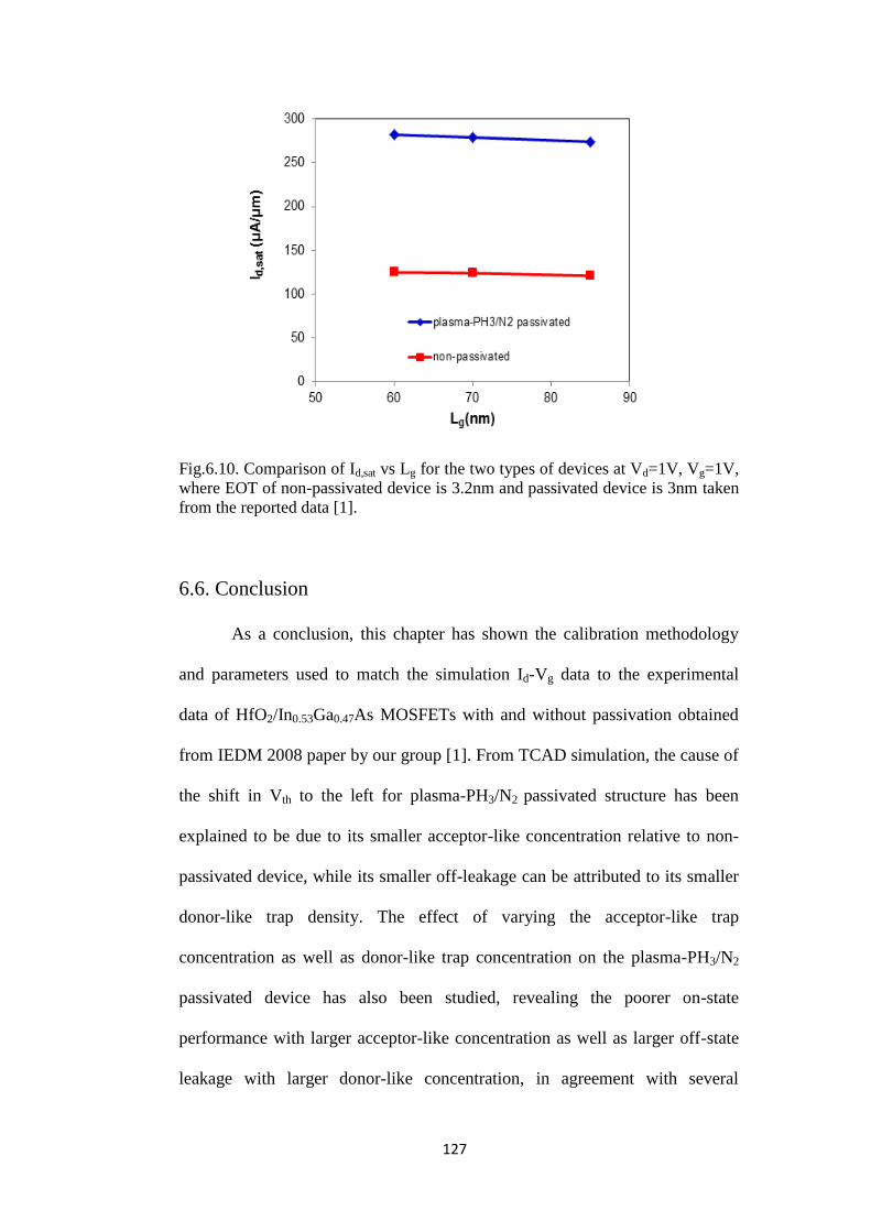
127
Fig.6.10. Comparison of Id,sat vs Lg for the two types of devices at Vd=1V, Vg=1V,
where EOT of non-passivated device is 3.2nm and passivated device is 3nm taken
from the reported data [1].
6.6. Conclusion
As a conclusion, this chapter has shown the calibration methodology
and parameters used to match the simulation Id-Vg data to the experimental
data of HfO2/In0.53Ga0.47As MOSFETs with and without passivation obtained
from IEDM 2008 paper by our group [1]. From TCAD simulation, the cause of
the shift in Vth to the left for plasma-PH3/N2 passivated structure has been
explained to be due to its smaller acceptor-like concentration relative to non-
passivated device, while its smaller off-leakage can be attributed to its smaller
donor-like trap density. The effect of varying the acceptor-like trap
concentration as well as donor-like trap concentration on the plasma-PH3/N2
passivated device has also been studied, revealing the poorer on-state
performance with larger acceptor-like concentration as well as larger off-state
leakage with larger donor-like concentration, in agreement with several

128
reported papers. With the current process flow, the on-state performance
scalability of plasma-PH3/N2 passivated device vs non-passivated device has
been simulated. On-state performance of passivated devices are higher than
corresponding non-passivated devices, with improvements to the SCE
charateristics attributed to reduced EOT and also reduced Dit. Nevertheless,
even at Lg=80nm the DIBL of plasma-PH3/N2 device is already 200mV/V but
with Id,sat of only 275µA/µm at Vg=1V, Vd=1V. This implies further
improvement to the device structure and process flow is necessary for further
improved device performance. These modifications will be explored in Chapter
7 through simulation using calibrated models presented in this chapter.

129
REFERENCES [1]J. Lin, S.J. Lee, H.J. Oh, W. Yang, G.Q. Lo, D.L. Kwong, and D.Z. Chi, “Plasma
PH3-passivated high mobility inversion InGaAs MOSFET fabricated with self-aligned
gate first process and HfO2/TaN gate stack”, Tech. Dig. – Int. Electron Devices Meet.,
pp.401, 2008.
[2]Taurus Medici, Medici User GuideVersion D-2010.03, March 2010.
[3]Y. Hwang, R. Engel-Herbert, N.G. Rudawski and S. Stemmer “Analysis of trap
densities at HfO2/ In0.53Ga0.47As interfaces”, Appl.Phys.Lett., Vol.96,102910, 2010.
[4]P.D. Ye“Main determinants for III–V metal-oxide-semiconductor field-effect
Transistors”, J. Vac. Sci. Technol. A, Vol. 26, No. 4, pp.700, 2008.
[5]G. Brammertz, A. Alian, H.C. Lin, L. Nyns, S. Sioncke, C. Merckling, W.E. Wang,
M. Caymax, T.Y. Hoffmann, “Electrical Quality of III-V/Oxide Interfaces: Good
Enough for MOSFET Devices?”, ECS Trans., Vol.34, No.1, pp.1017, 2011.
[6]Y. Hirota and O. Mikami “Energy barrier height measurements of chemically vapour
deposited P3N5 Films by Internal Photoinjection”, Thin Solid Films, Vol.162, pp.41-47,
1988.
[7]M. Levinshtein,S. Rumyantsev and M.Shur, “Handbook Series on Semiconductor
Parameters”, Vol.2.
[8] Lin Jianqiang, “Novel III-V MOSFET Integrated with High-k dielectric and metal
gate for Future CMOS Technology”, Masters Thesis, National University of Singapore,
2009.
[9]A. Alian, G. Brammertz, N. Waldron, C. Merckling, G. Hellings, H.C. Lin, W.E.
Wang, M. Meuris, E. Simoen, K. De Meyer and M. Heyns “Silicon and selenium
implantation and activation in In0.53Ga0.47As under low thermal budget conditions”,
Microelectronic Eng., Vol.88, pp.155–158, 2011.
[10]Y.Q. Wu, M. Xu, R.S. Wang, O. Koybasi and P.D. Ye, “High Performance Deep-
Submicron Inversion-Mode InGaAs MOSFETs with maximum Gm exceeding 1.1
mS/μm: New HBr Pretreatment and Channel Engineering”, Tech. Dig. – Int. Electron
Devices Meet., pp.323, 2009.
[11]B. Benbakhti, J.S. Ayubi-Moak, K. Kalna, D. Lin and G. Hellings, “Impact of
interface trap density on the performance characteristics of different III-V MOSFET
architecture”, Microelectronics Reliability., Vol.50, No.3, pp.360, 2010.
[12]D. Varghese, Y. Xuan, Y.Q. Wu, P.D. Ye, and M.A. Alam, “Multi-probe interface
characterization of In0.65Ga0.35As/Al2O3 MOSFET”, Tech. Dig. – Int. Electron Devices
Meet., pp. 379, 2008.
[13]Wang Weike, “Characterization of InGaAs Metal-Oxide-Semiconductor Field-
Effect Transistors”, PhD dissertation, Leigh University, 2011.
130
Chapter 7: Optimization Studies of plasma-PH3/N2 Passivated
In0.53Ga0.47As MOSFET for Sub-22nm Device Performance
7.1. Introduction and Motivation-Issues and Challenges
As transistors continue to scale aggressively in accordance with
Moore‘s Law to sub-22-nm dimensions, it is important to explore novel
channel materials and device structures that would lead to high performance
nanoscale MOSFETs that are reasonably energy-efficient. Due to their
significant transport advantage which allows high performance even at low
supply voltage, high mobility materials are being very actively researched as
channel materials for future highly scaled CMOS [1-8]. Thus, the idea of
introducing III-V material, in our work In0.53Ga0.47As, as channel material is
appealing.
However the device design considerations for In0.53Ga0.47As MOSFET
differ from that of a Si MOSFET for reasons explained here. The off-state
leakage and SCE of In0.53Ga0.47As MOSFET is expected to be worse than Si
due to its smaller bandgap, high band-to-band tunnelling leakage, and also
larger permittivity. In addition, the driving capability of In0.53Ga0.47As
MOSFETs may also be adversely affected because of their smaller density of
states (DOS) due to its small effective mass compared to Si. One effect of
small DOS is its reduction in scattering rate through having less final states for
carriers to scatter to, which slows down the replenishment process and leads to
a phenomenon seen in In0.53Ga0.47As MOSFET known as source starvation [9].
This effect can limit the sheet charge density at a given gate bias.
This chapter will make use of the same calibrated plasma-PH3/N2
In0.53Ga0.47As MOSFET presented in Chapter 6 for device optimization studies
using TCAD simulations. Section 7.2 would involve optimizing implanted S/D

131
(ISD) In0.53Ga0.47As MOSFET drive current capability by reducing access
resistance through the use of spacer and best case contact resistance achievable
in ISD In0.53Ga0.47As MOSFET. The device scalability of these ISD would be
further optimized through the use of source drain extension (SDE) as well as
halo doping in order to reduce the SCE. One of the limitations of ISD is the
low activation levels of silicon implanted in S/D (maximum 1x10¹⁹
cm-3
) which
further worsens the source starvation effects. Thus, Section 7.3 aims to reduce
these effects by using epitaxial-grown S/D (known as raised S/D i.e. RSD)
MOSFET which has the ability to incorporate high in-situ active doping
densities (4-10x1019
cm-3
) in In0.53Ga0.47As without high temperature anneals
[10-11]. It will be shown in Section 7.3.1 that by comparison of the RSD with
the optimized ISD, the reduction in source starvation helps in further
improving the drive current performance of the RSD In0.53Ga0.47As MOSFET.
In addition, RSD MOSFET has the benefit of improving the SCE compared to
optimized ISD and thus more potential for device scalability improvement.
From the RSD structure, further improvement to device performance has been
obtained with the use of thin channel (10nm) presented in Section 7.4. This is
due to the reduced inversion layer width caused by increased quantum
confinement which allows more electron carrier concentration to exist at the
channel.
However, for sub-22nm technology node, such RSD thin channel
structure at channel thickness (Tch) of 10nm is insufficient to maintain high
electrostatic integrity. This is based on the rule of thumb based on FDSOI
MOSFETs, that to maintain good SCE the channel thickness should be no
thicker than Lg/3 [12]. Hence, further channel thickness reduction is simulated
with additional simulations performed on heterostructure device and varying

132
spacer materials to enhance device performance with low SCE and low GIDL
shown in Section 7.5 down to Lg=14.nm.
7.2. Device Optimization of Implanted S/D In0.53Ga0.47As MOSFET
Two techniques were used to optimize the drive current capability of
the implanted S/D structure for this section. The first is reducing the Rc from
1200Ω.µm to 400Ω.µm. This value has been chosen based on the best
achievable contact resistance measured on implanted S/D In0.53Ga0.47As
MOSFET [13]. The second is including a spacer of 15nm width, achieved
through self-aligned technique, to reduce series access resistance by reducing
the gate–S/D contact spacing from 2µm in the original process flow. Also,
EOT has been reduced to 2nm for plasma-PH3/N2 device compared to 3nm in
the existing process flow in Chapter 6 to further increase the device
performance. In addition to these changes, ISD structure consists of halo
implant, S/D extension and deep S/D to obtain acceptable electrostatic integrity
with acceptable Id,sat compared to without halo. The halo implant is located
between the deep S/D and SDE as shown from the 1D plot taken at the S/D,
which is shown in Fig.7.1.
The realistic peak deep S/D concentration is chosen as 9x10¹⁸
cm-3
[14-
15]. Improvement in electrostatic integrity with halo implant can be observed
as shown in Fig.7.2(a) for Lg=70nm, giving DIBL of 226mV/V, 164mV/V and
103mV/V for devices without halo, with halo concentration of 7.2x10¹⁷
cm-3
and halo concentration of 2x10¹⁸
cm-3
respectively, implying that implementing
an even higher halo doping concentration of 2x10¹⁸
cm-3
would further improve
the DIBL. However, the drawback is the greater reduction in Ion as shown in
Fig.7.2(b) given as 979µA/µm, 914µA/µm and 643µA/µm at Vd=0.7V, Vg=1V

133
for devices without halo, with halo concentration of 7.2x10¹⁷
cm-3
and halo
concentration of 2x10¹⁸
cm-3
respectively. The improvements in electrostatic
integrity with larger halo implant concentration can be explained from the
potential contours plot (Figs.7.3(a)-(c)) and the conduction band energy plot
taken at 1nm below the PxNy/In0.53Ga0.47As interface (Fig.7.4). There are lesser
potential lines contributed by the S/D into the channel for Fig.7.3(a) and
Fig.7.3(b) compared to Fig.7.3(c), showing that control of S/D over the
channel is effectively improved by halo doping. The conduction band energy
profiles taken at 1nm below the interface show that the potential barrier faced
by source electrons is lower for the device without halo compared to that with
halo shown in Fig.7.4.
Fig.7.1. 1D Doping profile for the extension, SD and halo implants by taking a
vertical cut at the S/D.

134
.
Fig.7.2 (a) Id-Vg plot for plasma-PH3/N2 passivated Lg=70nm device with and
without halo implant and (b) Id-Vg plot in linear scale for plasma-PH3/N2
passivated device with and without halo implant. For devices with halo implant,
the peak concentration is given by 7.2x1017cm-3 and 2x1018cm-3.
(a)
(b)

135
Fig.7.3. 2D potential contours at Vg=0V and Vd=0.7V, for Lg=70nm (a) with halo
implant (7.2x1017cm-3) and (b) with halo implant (2x1018cm-3) and (c) without halo
implant.
Fig.7.4. Conduction band energy profile as a function of distance along the
channel taken at 1nm below the PxNy/In0.53Ga0.47As interface for Vd=0.7V at
Vg=0V.
(b) (a)
(c)

136
However, as halo doping increases, GIDL current increases which can be
clearly seen from the increased generation rate contours from the 2D plot in
Fig.7.5, attributed to higher halo doping concentration near the edge of the
channel. The min to max generation rate is defined as 1x1025
cm3/s to
1x1029
cm3/s with 5 contour lines, with a lateral mesh spacing of 0.2nm at
regions close to the S/D to channel edge so that the energy band diagram
would represent the true effects caused by GIDL. From Fig.7.6 it is found that
the minimum tunnelling width between channel and drain regions for halo
implant of 2x10¹⁸
cm-3
is 22.7nm while it is 29nm for halo implant of
7.2x10¹⁷
cm-3
. The smaller tunnelling width of device with halo implant of
2x10¹⁸
cm-3
initiates more tunnelling of electrons from the valence band of the
channel to the conduction band of the drain, resulting in greater GIDL. Hence,
this shows that despite improvement in electrostatic integrity with higher halo
doping concentration, this increase in drain leakage may present a difficulty for
planar In0.53Ga0.47As.
Fig.7.5. Simulation 2D BTBT generation contours at Vg=-0.3V and Vd=0.7V, for
Lg=70nm (a) with halo implant (7.2x1017cm-3) and (b) with halo implant
(2x1018cm-3).
(a) (b)

137
Fig.7.6. Band diagram in the lateral direction for plasma-PH3/N2 passivated
In0.53Ga0.47As MOSFETs with two different halo implant conditions, taken at
Vg=-0.3V, Vd=0.7V at maximum BTBT generation point. From 1D profile,
maximum BTBT generation occurs at x=3.6µm, y=0.01µm for Fig.7.5(a) and at
x=3.6µm, y=0.004µm for Fig.7.5(b).
7.3. Raised S/D In0.53Ga0.47As MOSFET
High mobility In0.53Ga0.47As N-MOSFETs require shallow, abrupt and
highly doped N+ S/D. Most In0.53Ga0.47As transistors use S/D implantation
through the use of Si as the n-type dopant because of its negligible diffusivity
which allows the realization of very abrupt junctions. However, the maximum
n-type carrier concentration in In0.53Ga0.47As with Si as dopants can only
reach ~1x10¹⁹
cm-3
by direct Si implantation due to the low solid
solubility limitation [14-15]. This doping level is far from the state-of-art
doping concentration (in the order of 1020
cm-3
) achieved for Si and thus
In0.53Ga0.47As transistors will suffer more from S/D series resistance as
compared with Si transistors. Thus, one of the motivations of studying regrown
S/D MOSFET is to reduce the contact resistance through heavy in-situ doping
during the selective epitaxy growth to obtain lower Rc. In addition, the higher

138
source doping concentration, together with its enlarged volume over which
scattering can redirect carriers into longitudinal k-states, is expected to solve
the source starvation issue, which is one of the results of DOS bottleneck
present in In0.53Ga0.47As devices.
The aim of this section is to investigate the effectiveness of RSD
in reducing the source starvation issue through comparison with optimized
halo-ISD MOSFET. In addition, the logic technology figures of merit (SS,
Vt,sat, DIBL, Ion/Ioff ratio, injection velocity (Vinj) and switching delay) would
also be studied to show significant improvement on device scalability with
RSD.
Fig.7.7. 2D plots of the (a) Implanted S/D MOSFET and (b) Raised S/D MOSFET
used in the simulation
The ISD and RSD device structures both use a 15nm wide Si3N4
spacer, with contact resistance of 400Ω.µm [13], as well as halo and SDE.
Also RSD structure here uses 30nm thick 6.5x10¹⁹
cm-3
doped S/D and with
InP material to benefit from its band discontinuity which can result in higher
carrier concentration in the channel [16]. RSD MOSFET does not include the
deep S/D because of the RSD structure already present. Both structures are
shown in Fig.7.7(a) and Fig.7.7(b). SDE is still needed for RSD because
extensions of undoped In0.53Ga0.47As below the sidewall spacers might
(a) (b)

139
introduce extra series resistance to the MOSFET. Comparison with and
without SDE at Vg-Vt,sat=0.5V, Vd=0.7V (recommended by ITRS) at
EOT=0.6nm for Lg=50nm device taken at 1nm below the PxNy/In0.53Ga0.47As
interface showing the amount of carrier concentration along the channel
direction is shown in Fig.7.8. Vd value between 0.5V to 0.8V is acceptable
based on the ITRS 2011 recommendation for III-V devices [17-18] because
high applied voltage (Vd=1.0V) can cause the energy of carriers to be larger
than the energy separation between Γ and L valley (due to the low density of
states in the In0.53Ga0.47As and is given as 0.46eV) which increases the
contribution of L valley‘s electrons in the electron transport. This can reduce
the device performance due to low mobility of the electrons in the L valley
[19].
It is seen from Fig.7.8 that without SDE, electron spill over from the
N+ source layer which provides the necessary carriers under the sidewall
spacer is insufficient to provide sufficiently large on-state performance of the
device. The amount of electron concentration under the spacer is only
1.2x10¹⁸
cm-3
, at the lowest point between the beginning and end of spacer for
without SDE, compared to 3.6x10¹⁸
cm-3
with SDE added, thus resulting in
larger access resistance. The amount of inversion electron concentration (Ninv)
inside the channel is also larger with presence of SDE, implying that source
starvation, can be reduced. This reduction in electron concentration below the
spacer is also not completely compensated by the increase of the velocity
shown in Fig.7.9. The average velocity inside the channel is almost the same
for both SDE and without SDE, possibly due to the enhanced channel field
being offset by a reduction in the injection velocity from the source due to
increased impurity scattering for the structure with SDE [20]. Hence, due
mainly to lesser effect of source starvation in structure with SDE, the drive

140
current with SDE is increased from 177.6µA/µm to 586.8µA/µm for with SDE
over that without SDE.
Other than the use of SDE and reducing the spacer width to increase the
electron concentration below the spacer, the use of pulse doping in the back
barrier or recessed/undercut regrowth of SD below the sidewall can provide
more electrons in this region to reduce the source access resistance [11,21].
Fig.7.8. Inversion electron concentration at 1nm below PxNy/In0.53Ga0.47As
interface taken along the channel direction at Vg-Vt,sat=0.5V, Vd=0.7V for
Lg=50nm for EOT=0.6nm.
Fig.7.9. Average electron velocity along the channel of the In0.53Ga0.47As
MOSFET taken at 1nm below PxNy/In0.53Ga0.47As interface and at Vg-Vt,sat=0.5V,
Vd=0.7V for Lg=50nm, EOT=0.6nm.

141
7.3.1. Source starvation and Performance Scalability of RSD vs ISD Devices
Fig.7.10 plots the performance of both ISD and RSD devices with
scaling, as a function of different EOT to show the improvement to the device
performance brought about by improved gate control. ISD shows smaller drive
current compared to RSD for the same device gate length, reflecting the source
starvation effects more dominant in ISD MOSFETs. RSD has higher potential
of mitigating this source starvation effect and this can be seen from Fig.7.11(a)
which plots Ninv vs distance along channel comparing ISD and RSD for
Lg=50nm at EOT=0.6nm showing that the inversion electron carrier
concentration inside the channel is larger for RSD. This is because RSD has
higher doped source which supplies more carriers which can be scattered and
redistributed into the channel direction [20]. In addition, the geometry of the
RSD structure itself increases the acceptance cone which thus effectively
enlarges the volume over which scattering can redirect carriers into the
longitudinal states [9]. On the other hand, the average velocity inside the
channel is almost unchanged for RSD and ISD devices described in
Fig.7.11(b). Thus, due to the smaller source starvation effect in RSD, the drive
current of RSD MOSFET significantly increased compared to ISD MOSFET.
In addition from Fig.7.10, ISD shows larger drive current degradation with
scaling, reflecting the poorer SCE relative to RSD MOSFET.
Despite the Id,sat degradation with device scaling, the intrinsic gate delay
given as CV/I improves with scaling, where it is calculated using
Cox*L*Vd/Id,sat. However, the values are still considerably larger compared to
ITRS of only 0.13ps for Lg=22nm at Vd=0.7V. Hence, to further improve
driving capability, the use of lower contact resistance achievable in InP RSD

142
[16], compared to ISD, and also thinner channel thus with increased quantum
confinement, will be useful to be studied as shown in the next section.
Fig.7.10. Channel length and EOT dependences of Id,sat and CV/I shows far better
performance of RSD over conventional ISD. Id,sat taken at Vd=0.7V,
Vg-Vt,sat=0.5V.
The improvement in threshold voltage roll off and DIBL (difference in
threshold voltage measured at Vd=0.7V and Vd=0.05V) of RSD is also shown
in Fig.7.12. The addition of RSD prevents the need for the deep S/D, thus
reducing the total donor doping concentration near the channel. The potential
contours plot, seen in Fig.7.13 which is taken at Lg=50nm for Vd=0.7V and
Vg=0V, shows that there are less potential contour lines contributed by the S/D
into channel, hence improving the DIBL. Further analysis of the conduction
band energy plot in Fig.7.14 reveals the larger barrier height that needs to be
overcome by the electrons as it enters the channel, in the RSD MOSFET
compared to the ISD MOSFET, thus explaining the better short channel effect
behaviour of the RSD MOSFET. In addition, due the contribution of deep SD
concentration, the total donor concentration near the edge of the spacer is

143
larger for ISD MOSFET resulting in the electron flow lines to exist at the
region close to the spacer while RSD MOSFET has electron flow lines starting
and ending at the region only beyond the spacer shown in Fig.7.15, hence
further explaining the DIBL improvement. The relationship between Ion and Ioff
was also investigated in Fig.7.16 showing the benefits of RSD structure. SS is
improved by the addition of RSD due to the better gate control on the channel
potential.
Fig.7.11 (a) Comparison of inversion electron concentration between RSD and ISD
MOSFETs, where Lg=50nm, Vg-Vt,sat=0.5V and Vd=0.7V and (b) Comparison of
average electron velocity between RSD and ISD MOSFETs, where Lg=50nm,
Vg-Vt,sat=0.5V and Vd=0.7V.
(a)
(b)
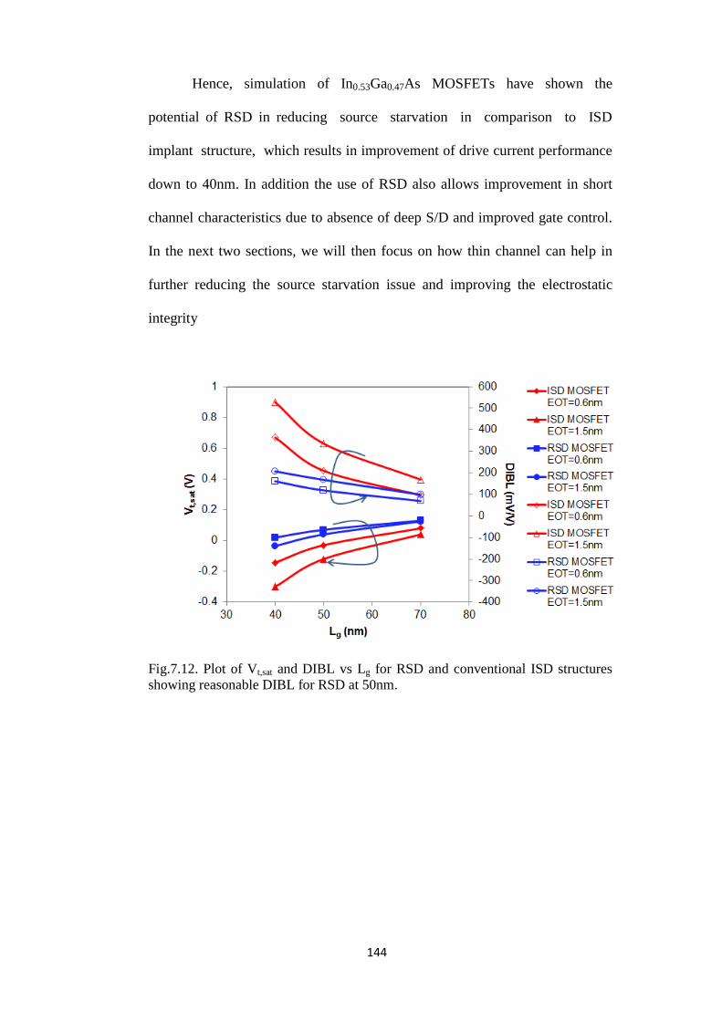
144
Hence, simulation of In0.53Ga0.47As MOSFETs have shown the
potential of RSD in reducing source starvation in comparison to ISD
implant structure, which results in improvement of drive current performance
down to 40nm. In addition the use of RSD also allows improvement in short
channel characteristics due to absence of deep S/D and improved gate control.
In the next two sections, we will then focus on how thin channel can help in
further reducing the source starvation issue and improving the electrostatic
integrity
Fig.7.12. Plot of Vt,sat and DIBL vs Lg for RSD and conventional ISD structures
showing reasonable DIBL for RSD at 50nm.

145
Fig.7.13. 2D potential contour plot of (a) RSD In0.53Ga0.47As MOSFET and (b)
ISD In0.53Ga0.47As MOSFET for Lg=50nm taken at Vg=0V, Vd=0.7V.
Fig.7.14. Conduction band energy profiles for RSD In0.53Ga0.47As MOSFET and
ISD In0.53Ga0.47As MOSFET for Lg=50nm taken at Vg=0V, Vd=0.7V and taken at
1nm below the PxNy/In0.53Ga0.47As interface.
(a) (b)

146
Fig.7.15. Electron flowlines for (a) RSD In0.53Ga0.47As MOSFET and (b) ISD
In0.53Ga0.47As MOSFET for Lg=50nm taken at Vg=0V, Vd=0.7V. Electron
flowlines in (a) do not start from within the spacer at the source unlike in (b).
Fig.7.16. Plot of SS and Ion /Ioff ratio vs Lg for RSD and ISD N-MOSFETs.
7.4. Performance Scaling with Raised S/D and In0.53Ga0.47As Thin
Channel MOSFET
Previous sections have shown that SCE in In0.53Ga0.47As is one of the
most important effects limiting MOSFET scalability, and to achieve sub-50nm
gate length, very high body doping is required. However, high doping in the
channel region is harmful to the device performance in both thick and thin
body substrates due to mobility degradation [22-23]. Besides significant
(a) (b)

147
mobility degradation, the high body doping also leads to the issue of band-to-
band tunneling which is dependent on electric field and also energy bandgap.
Therefore, with the limitations imposed on the doping levels on thin channel
MOSFETs, lightly doped (p-type 5x10¹⁵
cm-3
) In0.53Ga0.47As thin channel
MOSFET with lightly doped buffer layer (p-type 5x10¹⁵
cm-3
) and without halo
doping would be studied.
Fig.7.17. Electron density distribution in the inversion layers for In0.53Ga0.47As bulk and thin channel MOSFET for Lg=40nm at EOT=0.6nm. Note that 0.03µm corresponds to the PxNy/In0.53Ga0.47As interface and vertical distance from surface refers to distance away from PxNy/In0.53Ga0.47As interface. Plot has been taken at the center of the channel.
A 10nm In0.53Ga0.47As thin channel MOSFET up till Lg=40nm has been
studied with contact resistance of 93Ω.µm achievable for raised S/D structure
[2]. Fig.7.17 shows larger peak electron concentration in the inversion layer
with thin channel, due to reduced width of inversion layer caused by larger
quantum confinement, compared to bulk device.
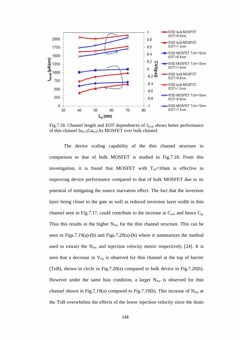
148
Fig.7.18. Channel length and EOT dependences of Id,sat shows better performance of thin channel In0.53Ga0.47As MOSFET over bulk channel.
The device scaling capability of the thin channel structure in
comparison to that of bulk MOSFET is studied in Fig.7.18. From this
investigation, it is found that MOSFET with Tch=10nm is effective in
improving device performance compared to that of bulk MOSFET due to its
potential of mitigating the source starvation effect. The fact that the inversion
layer being closer to the gate as well as reduced inversion layer width in thin
channel seen in Fig.7.17, could contribute to the increase in Cinv and hence Cg.
Thus this results in the higher Ninv for the thin channel structure. This can be
seen in Figs.7.19(a)-(b) and Figs.7.20(a)-(b) where it summarizes the method
used to extract the Ninv and injection velocity metric respectively [24]. It is
seen that a decrease in Vinj is observed for thin channel at the top of barrier
(ToB), shown in circle in Fig.7.20(a) compared to bulk device in Fig.7.20(b).
However under the same bias condition, a larger Ninv is observed for thin
channel shown in Fig.7.19(a) compared to Fig.7.19(b). This increase of Ninv at
the ToB overwhelms the effects of the lower injection velocity since the drain

149
current can be expressed as Id=q*Vinj*Ninv where q is the elementary charge.
Hence, Id,sat performance of thin channel device is still higher despite the
reduction in injection velocity. This reduced Vinj in thin channel may be due to
the increased quantum confinement in the channel layer that increases the
back-scattering rate which further reduces the velocity along the channel [19].
In addition, it is seen that the decrease of Id,sat with device scaling is
significantly reduced with thin channel structures as seen in Fig.7.18. This
implies the importance of increased Ninv near the source in addition to
improved SCE to ensure increase in Id,sat with device scaling.
In addition, the Vt,sat roll off and DIBL characteristics of the thin
channel vs bulk structure as a function of EOT is shown in Fig.7.21.
MOSFETs with thin channel exhibit lower Vt,sat roll off and DIBL compared to
bulk structure, and that EOT scaling is still effective to achieve good
electrostatic characteristics. The reason for the larger Vt,sat for thin channel
compared to bulk is caused by the presence of quantum mechanical
confinement of carriers in the thin channel layer which increases the sub-band
energy level. Also, the lower SS in Fig.7.22 further shows the improvement in
the electrostatic integrity of the thin channel MOSFET compared to bulk
MOSFET. Fig.7.22 also shows the improvement in Ion/Ioff caused by the
improved on-current of thin channel MOSFET.
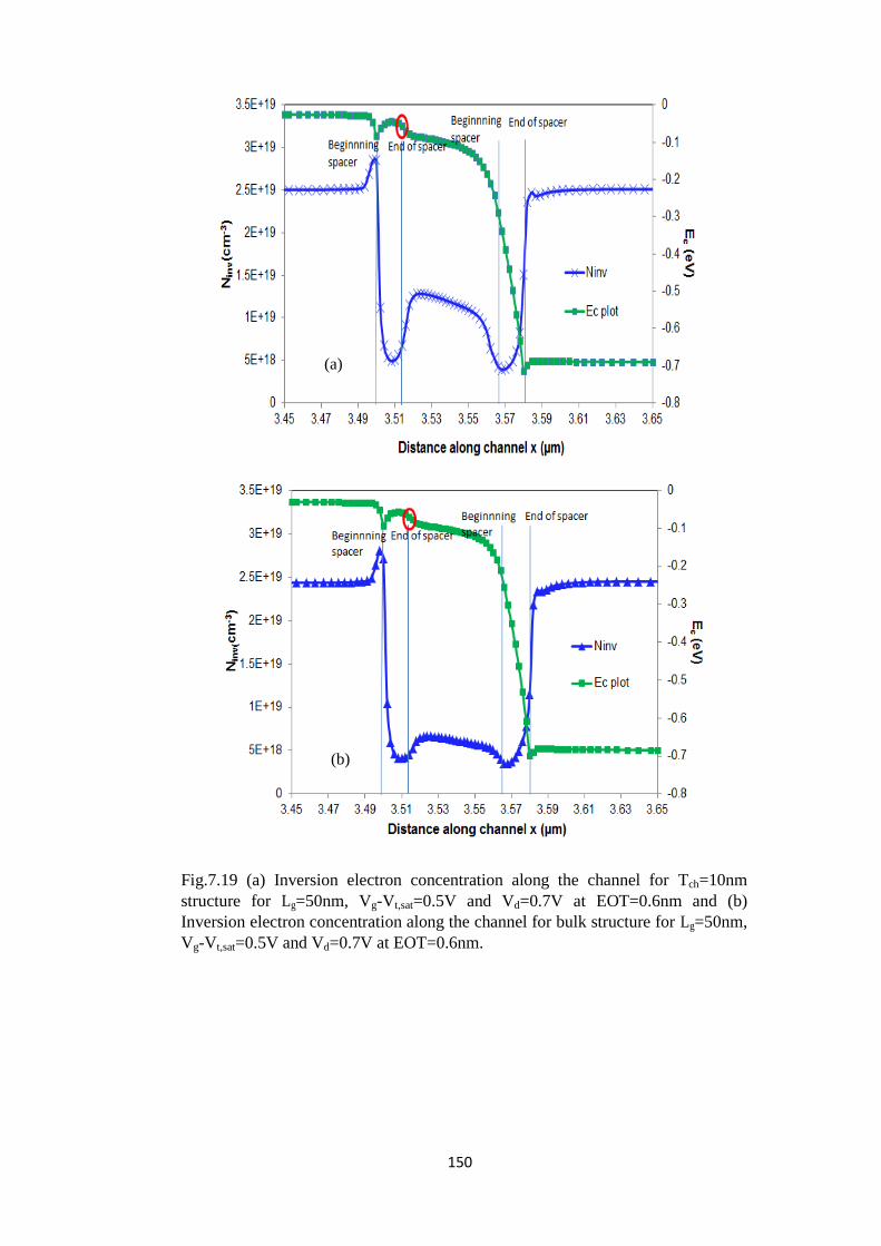
150
Fig.7.19 (a) Inversion electron concentration along the channel for Tch=10nm
structure for Lg=50nm, Vg-Vt,sat=0.5V and Vd=0.7V at EOT=0.6nm and (b)
Inversion electron concentration along the channel for bulk structure for Lg=50nm,
Vg-Vt,sat=0.5V and Vd=0.7V at EOT=0.6nm.
(a)
(b)

151
Fig.7.20 (a) Average electron velocity along the channel for Tch=10nm structure
for Lg=50nm, Vg–Vt,sat=0.5V and Vd=0.7V at EOT=0.6nm and (b) Average
electron velocity along the channel for bulk structure for Lg=50nm, Vg-Vt,sat=0.5V
and Vd=0.7V at EOT=0.6nm.
(a)
(b)

152
Fig.7.21. Plot of Vt,sat and DIBL vs Lg for thin channel and bulk In0.53Ga0.47As
MOSFET.
Fig.7.22. Plot of SS and Ion /Ioff ratio vs Lg for RSD bulk and thin channel MOSFETs.

153
7.5. Optimization of In0.53Ga0.47As MOSFET Device Structures for
Performance Scalability up till Sub-22nm Technology Node
Despite the improvement in electrostatic integrity and device
performance with the use of thin channel=10nm as shown in the previous
section, the DIBL of Lg=40nm is already large at ~95mV/V even with
EOT=0.6nm shown in Fig.7.21. In order for future scaling to sub-22nm to
continue with acceptable electrostatic integrity given by leakage of 0.1µA/µm
at Vg=0V, and Id,sat=2A/mm at Vd=0.7V and Vg-Vt,sat=0.5V as predicted by
ITRS 2011, further device engineering is needed. This includes studies on
further scaling of channel thickness, the addition of heterostructure layer for
acceptable Id,sat as well as spacer material for GIDL reduction. All these
changes are made with the aim of predicting the In0.53Ga0.47As performance of
22nm to 14nm gate length device.
The design of the device needed for sub-22nm is mentioned based on
the device architecture for each part of the device which has been explained in
the first few sections. First, raised S/D is necessary to help alleviate source
starvation effects by increasing the chance of electrons to occupy the
longitudinal k-states near the channel. Second, unintentionally doped thin
channel with unintentionally doped InP buffer layer, is required to improve the
SCE without affecting the mobility and hence Ion of the device. Hence, based
on these, a cross section of the baseline structure is shown in Fig.7.23, with the
gate dielectric chosen as EOT=0.6nm. The top In0.53Ga0.47As channel layer will
be varied from 12nm to 3nm as shown in Section 7.5.1 as well as addition of
top and bottom In0.52Al0.48As capping layer to form heterostructure device as
shown in Section 7.5.3.

154
Fig.7.23. Device design of the structure simulated.
The performance of the device which includes Id,sat, DIBL and SS have
been systematically studied based on the different variations from the baseline
structure. The variations are with 1) Effects of reduced Tch 2) Spacer material
to improve GIDL and 3) Addition of In0.52Al0.48As top and bottom capping
layer (Heterostructure Device). Finally, the structure would be compared and
benchmarked to the structures simulated by other groups. Based on the ITRS
roadmap, III-V technology devices have Vd of between 0.5 to 0.8V and hence,
Vd=0.7V has been studied for this section.
7.5.1. Effect of Thinner channel
As Tch reduces to 3nm, the Id,sat at the same Ioff of 0.1µA/µm increases
as seen in Fig.7.24. The performance enhancement is due to the smaller
inversion layer thickness owing to the physical confinement of the electron
wave function within the quantum channel. To demonstrate this, Fig.7.25
shows the electron distributions in the inversion layers computed for each
device structure with the gate bias voltages given as 0.7V and drain voltage set
at 0.7V. The electrons are seen to be confined in the ultrathin channel region
by the InP buffer layer, thus causing the inversion layer width to decrease

155
leading to increase of inversion layer capacitance and hence gate capacitance.
Therefore the drive current in the thin channel MOSFET increases as Tch
reduces. The improvement of DIBL and SS as a function of Tch is shown in
Fig.7.26. DIBL and SS is smaller as Tch reduces due to minimum electric field
from the drain penetration contributing to reduction of potential contours from
the S/D to the channel shown in Fig.7.27(a) and Fig.7.27(b) and higher
potential barrier from the source to the channel in Fig.7.28 for Tch=3nm
compared to Tch=12nm. The SS improves with reduced Tch due to the stronger
quantum confinement which moves the peak of the inversion layer width
towards the high-k/In0.53Ga0.47As interface which improves the gate control
[25].
The channel thickness of 3nm is chosen because severe SCE is
observed with Tch of 5nm especially at Lg=14nm. The SS and DIBL of
Tch=3nm In0.53Ga0.47As MOSFET does not significantly degrade as the Lg
reduces, while the SS characteristics of Tch=5nm and 12nm start to degrade
significantly when Lg drops below 22nm and 28nm respectively. This is due to
improved SCE control with thinner channel.
However, one expected issue with scaling of channel thickness is the
excessive quantization effect in thinner body (especially less than 5nm) that
can cause carriers to travel in the higher mass L valley, where the %
contribution of electrons in the drive current from the L valley can be as high
as 18% for Tch=3nm for Vd =1V, at gate overdrive=0.7V [26]. This effect can
result in degradation in device performance. However, due to the lower supply
voltage of 0.7V used in this work, it is expected that insignificant contribution
of L valley electrons to the operation of the In0.53Ga0.47As device. In order to
reduce this quantization effect, other device structures that can achieve high Ion

156
and acceptable SCE without using channel thickness below 5nm is needed in
order for In0.53Ga0.47As to be competitive over Si. They include structures like
double gate MOSFET and FINFET.
Fig.7.25. Electron density distributions in the inversion layers computed for thin
channel MOSFETs as a function of channel thickness at Vd=0.7V, Vg=0.7V.
These profiles have been extracted at the middle of the channel region.
Fig.7.24. Id-Vg plot as a function of channel thickness for Vd=0.7V at fixed Ioff of
0.1µA/µm.

157
Fig.7.26. SS and DIBL vs Lg characteristics as a function of channel thickness.
Fig.7.27. Potential contours for Lg=22nm with (a) Tch=12nm and (b) Tch=3nm
taken at Vd=0.7V, Vg=0V.
(a) (b)

158
Fig.7.28. Conduction band energy vs distance along the channel comparing
Tch=12nm and Tch=3nm for Lg=22nm device taken at Vd=0.7V, Vg=0V.
7.5.2. Effect of Spacer Material
Figs.7.29(a)-(c) shows the three different MOSFET structures used for
the analysis of the GIDL characteristics. The structure in Fig.7.29(a) has a
high-k dielectric and Si3N4 spacers used in the simulations studied so far, while
Fig.7.29(b) has high-k gate dielectric extended to the bottom of the spacers and
in Fig.7.29(c) both the gate oxide and spacer are of high-k HfO2 material. In
this section of the simulation work, the physical gate length is fixed at 22nm.
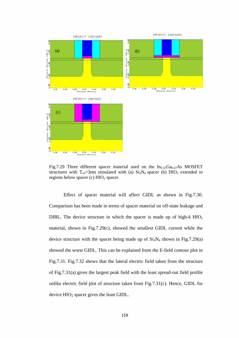
159
Fig.7.29 Three different spacer material used on the In0.53Ga0.47As MOSFET
structures with Tch=3nm simulated with (a) Si3N4 spacer (b) HfO2 extended to
regions below spacer (c) HfO2 spacer.
Effect of spacer material will affect GIDL as shown in Fig.7.30.
Comparison has been made in terms of spacer material on off-state leakage and
DIBL. The device structure in which the spacer is made up of high-k HfO2
material, shown in Fig.7.29(c), showed the smallest GIDL current while the
device structure with the spacer being made up of Si3N4 shown in Fig.7.29(a)
showed the worst GIDL. This can be explained from the E-field contour plot in
Fig.7.31. Fig.7.32 shows that the lateral electric field taken from the structure
of Fig.7.31(a) gives the largest peak field with the least spread-out field profile
unlike electric field plot of structure taken from Fig.7.31(c). Hence, GIDL for
device HfO2 spacer gives the least GIDL.

160
Fig 6.34. Id-Vg plot for the three different spacer materials studied
Fig.7.30. Id-Vg characteristics showing DIBL and GIDL with comparison with the
three types of spacer material.
1.00E-08
1.00E-06
1.00E-04
1.00E-02
1.00E+00
1.00E+02
-0.3 -0.2 -0.1 0 0.1 0.2 0.3 0.4 0.5 0.6 0.7
I d(µ
A/µ
m)
Vg(V)
Lg=22nm with fig (a) Vd=0.7V
Lg=22nm with fig (a) Vd=0.05V
Lg=22nm with fig (b) Vd=0.7V
Lg=22nm with fig (b) Vd=0.05V
Lg=22nm with fig (c ) Vd=0.7V
Lg=22nm with fig (c ) Vd=0.05V
Fig.7.31. 2D electric field plot taken at Vg=-0.3V, Vd=0.7V comparing the
structure with three different spacer materials with (a) Si3N4 spacer (b) HfO2
extended to regions below spacer (c) HfO2 spacer.

161
Fig.7.32. Electric field contours taken at 1nm below the PxNy/In0.53Ga0.47As
interface at the region along the channel with Vg=-0.3V and Vd=0.7V. Here the
electric field taken from Fig.7.31(a), especially at the region of the channel/drain
interface, shows the most focused and abrupt field while the electric field taken
from Fig.7.31(c) shows a laterally spread field which is responsible for its smaller
GIDL.
7.5.3. Effect of Heterostructure Device
In this structure, narrow bandgap In0.53Ga0.47As material is sandwiched
between the two wide-bandgap barrier layers with the channel confined at the
heterostructure interface. The barrier layer used is In0.52Al0.48As which has a
conduction band offset of 0.48eV with the In0.53Ga0.47As. The III-V barrier
layers are needed to provide (i) carrier confinement in the quantum well and
(ii) minimized off-state leakage current. The heterostructure design with
In0.53Ga0.47As channel on wide bandgap In0.52Al0.48As is used to cut down drain
to body leakage to reduce Ioff and to induce strong confinement to result in
higher mobility. The wide bandgap top capping layer i.e. In0.52Al0.48As layer
between channel and dielectric, is used to insulate the channel charge from the
effect of traps and scattering in the dielectric/III-V interface. It was kept

162
intentionally thin for this work at 1nm so as to avoid any spillover of charge
from the channel layer with high mobility into the wide bandgap low mobility
layer. Note that device with heterostructure would consist of top and bottom
In0.52Al0.48As capping layers i.e. layer 1 (a 1nm thick In0.52Al0.48As capping
layer between PxNy and In0.53Ga0.47As channel layer) and layer 2 (1nm thick
In0.52Al0.48As barrier layer between In0.53Ga0.47As channel layer and InP). This
has been based on the design of III-V heterostructure double gate MOSFET
[27] except that a single gate MOSFET has been simulated in this work. In
addition, high-k spacers are used based on Section 7.5.2 where GIDL is
reduced.
Reported from various groups which carried out experiments on
heterostructure InxGa1-xAs MOSFETs, increment in mobility of the structures
with capping layer is between 35% to 60% for 2nm InP/In0.7Ga0.3As [28] and
1nm InP/In0.7Ga0.3As [29] respectively caused by the reduced effect of Dit at
the high-k/InxGa1-xAs interface. Thus we have chosen a 50% higher mobility in
heterostructure than no heterostructure device for this work. This has been
based on the reported 1nm InP/In0.7Ga0.3As with CBO of 0.411eV [30]. Hence,
In0.52Al0.48As/In0.53Ga0.47As used in our work should have CBO of 0.48eV
based on In0.53Ga0.47As affinity of 4.51eV and In0.52Al0.48As affinity of 4.03eV
[30]. Since 1nm InP/In0.7Ga0.3As with CBO of 0.411eV has an increase in
mobility of 60%, our In0.52Al0.48As/In0.53Ga0.47As with CBO of 0.479eV should
have at least similar if not larger increase in mobility. However, this is
assuming that In0.52Al0.48As is not reactive with the high-k oxide, since it has
been reported that InxAl1-xAs usually has the problem of excessive aluminium
oxidation for ex-situ process [30]. Nevertheless, since PxNy capping layer
163
would be used as a barrier layer between high-k oxide and In0.52Al0.48As, this
excessive reaction of In0.52Al0.48As with the high-k oxide may be minimal.
The tradeoff of heterostructure device is that the gate to channel
distance is increased leading to a reduced gate control over the channel,
potentially degrading the short channel device performance. Subthreshold
slope for 22nm device at Vd=0.7V is seen to increase from 78.6mV/dec to
82.7mv/dec while DIBL increases from 89.7mV/V to 115mV/V from
Fig.7.33(a) for no heterostructure and heterostructure device respectively.
However, the Id,sat at Vg-Vth=0.7V seen in Fig.7.33(b) linear scale is
2400µA/µm for heterostructure device and is given by 1950µA/µm for non-
heterostructure device, which represents a 23% increase in Id,sat with the use of
heterostructure.

164
Fig.7.33. Id–(Vg-Vth) plot for (a) Vd=0.7V and Vd=0.05V, for Lg=22nm devices
with and without heterostructure in log scale and (b) Vd=0.7V and Vd=0.05V, for
Lg=22nm devices with and without heterostructure in linear scale.
7.5.4. Performance Scalability of Device With and Without
Heterostructure and Benchmarking
Thus based on the device advantages of optimizing certain parts of the
device architecture discussed in previous sections, this section would make use
of optimized structure with high-k spacer, at EOT=0.6nm, Tch=3nm, with and
without heterostructure for benchmarking with simulation works performed by
other groups. The studies would involve gate lengths between 28nm to 14nm.
Fig.7.33. Id–(Vg-Vth) plot for (a) Vd=0.7V and Vd=0.05V, for Lg=22nm devices
with and without heterostructure in log scale and (b) Vd=0.7V and Vd=0.05V, for
Lg=22nm devices with and without heterostructure in linear scale.
(a)
(b)
165
SCE is significantly suppressed in terms of Vt,sat roll off and DIBL for
devices without heterostructure seen in Fig.7.34. It can be observed for
Lg=14nm, the DIBL of device without heterostructure is 147mV/V while
heterostructure device has DIBL of 188.8mV/V. Fig.7.35 shows an increase of
SS of device with heterostructure from 95.2mV/dec compared to 88.4mV/dec
for device without heterostructure. The worsened electrostatic integrity of the
device with capping layer is likely due to the increased CET caused by the
presence of the lower k value of In0.52Al0.48As capping layer between the PxNy
and In0.53Ga0.47As channel. The Ion/Ioff for no heterostructure device shows a
sufficiently large value of 5.94x10⁵ for Lg=14nm and 9.25x10
5 for Lg=22nm
implying the good electrostatic control with sufficiently large Ion. On the other
hand, Ion/Ioff of heterostructure device is smaller at 1.25x10⁵ for Lg=14nm and
5.18x10⁵ for Lg=22nm due to the worse electrostatic integrity compared to
device without heterostructure.
Fig.7.36 shows Id,sat at Vd=0.7V, Vg-Vt,sat=0.5V is given by 945µA/µm
and 1067µA/µm, and at Vg-Vt,sat=0.7V is given by 1600µA/µm and
1775µA/µm, for Lg=14nm and Lg=22nm respectively of device without
heterostructure. On the other hand, device with heterostructure has Id,sat at
Vd=0.7V, Vg-Vt,sat=0.5V given by 875µA/µm and 1160µA/µm, and at Vg-
Vt,sat=0.7V given by 1670µA/µm and 2090µA/µm, for Lg=14nm and Lg=22nm
respectively. These values are still smaller than ITRS which requires 2,200
µA/µm at supply voltage of 0.7V and gate overdrive of Vg-Vt,sat=0.5V for III-V
NMOSFET. Hence, more improvements are still required such as increasing
Indium concentration and changing device architecture to obtain the
requirements set by ITRS. Despite the reduction in Id,sat with scaling, the CV/I
intrinsic delay improves with scaling. The reduction in Id,sat with scaling is
166
likely contributed by the worsened electrostatic integrity (causing the
significant Vt,sat roll off) as seen in Fig.7.37. Here at longer channels where roll
off is not significant i.e. from 160nm to 50nm, the Id,sat increases with smaller
channel lengths. This shows the increasing need for improved device
architecture to minimize SCE especially as Lg approaches the sub-22nm
technology node in order to ensure continuous improvement in Id,sat with gate
length scaling and hence improve device scalability. Such architectures may
include FINFET, triple gate or double gate structures. Note that the Figs.7.34-
7.37 have been taken from the plots of Figs.7.38(a)-(b) and Figs.7.39(a)-(b).
Table 7.1 benchmarking of this work performed with other simulation
works in Ref [26] shows that this work has poorer electrostatic integrity due to
lower p-type channel doping concentration of 5x10¹⁵
cm-3
compared to
2x10¹⁸
cm-3
in Ref [26] and also larger EOT of 0.6nm compared to 0.44nm in
Ref [26]. Nevertheless, the electrostatic integrity obtained in this work is still
acceptable, with higher Id,sat which has been reduced in Ref [26] caused by its
higher channel doping concentration. This lower Id,sat is despite its larger RSD
doping concentration of 1x10²⁰
cm-3
and idealized contact resistance.
Comparison of this work with single gate In0.75Ga0.25As UTB structure
in Table 7.1 shows that Ref [24] has lower Id,sat despite its higher Indium
concentration. This is likely due to the smaller RSD doping concentration used
at 5x10¹⁹
cm-3
[24] compared to 6.5x10¹⁹
cm-3
in addition to larger spacer width
of 20nm [24] in comparison to 15nm for this work. In addition, poorer
electrostatic integrity is observed due to the higher Indium concentration used
as the channel and slightly smaller Lg of 12nm. Nevertheless, Ref [24] shows
the potential of double gate UTB in improving on-state current and
electrostatic integrity despite increased channel thickness to 5nm compared to

167
3nm for the single gate devices.
Fig.7.35. SS and Ion/Ioff a function of gate length for device with and without
heterostructure.
Fig.7.34. Electrostatic integrity as a function of gate length for device with and
without heterostructure. Heterostructure device shows slightly worse SCE
compared to without heterostructure.

168
Fig.7.36. Id,sat and CV/I plots for device without heterostructure as a function of Lg
with Id,sat taken at Vd=0.7V, Vg-Vt,sat=0.5V.
Fig.7.37. Plot of Vt,sat and Id,sat as a function of Lg for Vd=0.7V, Vg-Vt,sat=0.5V. Lg
below 50nm shows the region where the electrostatic effect from the drain
becomes significant, resulting in significant roll off as well as causing reduced
drive current with scaling.

169
Fig.7.38 (a) Id-Vg plot of device without heterostructure for Lg=14nm, 22nm and
28nm taken at Vd=0.7V and (b) Linear scale plot of Id-(Vg-Vt,sat) for device
without heterostructure for Lg=14nm, 22nm and 28nm taken at Vd=0.7V.
(a)
(b)

170
Fig.7.39 (a) Id-Vg plot of device with heterostructure for Lg=14nm, 22nm and
28nm taken at Vd=0.7V and (b) Id-(Vg-Vt,sat) plot of device with heterostructure for
Lg=14nm, 22nm and 28nm taken at Vd=0.7V.
(a)
(b)

171
Table 7.1 The electrical data benchmarked against the simulation work performed
by other groups [24,26] for Lg~15nm. Id,sat is referring to Vg-Vth=0.7V when
comparison is made to Ref [26] and Id,sat is referring to Vg=0.7V at fixed Ioff of
0.1µA/µm when comparison is made to Ref [24].
7.6. Conclusion
As a conclusion for this chapter, we have optimized the self-aligned
surface channel plasma-PH3/N2 passivated In0.53Ga0.47As-based MOSFETs
with implanted S/D. Further optimization through the use of raised S/D
resulted in improvement to the electrostatic integrity as well as higher ability to
prevent carrier starvation compared to device with implanted S/D. We have
also investigated the effects of reducing the contact resistance, addition of
spacer and reduced channel thickness of 10nm on device performance. It is
found that with thin channel, Id,sat for thin channel is found to be larger than
that of bulk structure, due to its higher carrier concentration brought about by
stronger quantum confinement. Finally further device optimization has been
carried out for prediction of 22nm and 14nm gate length In0.53Ga0.47As
MOSFETs which includes further thinning down of device channel to 3nm,
varying spacer material and implementation of heterostructure device
(compared to without heterostructure device). Results benchmarked with other
groups’ simulation works show results simulated are comparable and further
improvement is expected with improved device architecture and higher Indium

172
concentration. In addition, to ensure continuous current increase with scaling,
it is necessary for non-planar device structures or IF-QWFET capable of
limiting the SCE be implemented.

173
REFERENCES [1]E. Hwang, S. Mookerjea, M.K. Hudait and S. Datta, “Investigation of scalability of
In0.7Ga0.3As quantum well field effect transistor (QWFET) architecture for logic
applications”, Solid State Elec., Vol.62, pp.82-89, 2007.
[2]M. Egard, L. Ohlsson, B.M. Borg, F. Lennck , R. Wallenberg, L.E. Wernersson and
E. Lind, “High Transconductance Self-Aligned Gate-Last Surface Channel
In53Ga0.47As MOSFET”, Tech. Dig. – Int. Electron Devices Meet, pp.13.2.1, 2011.
[3]U. Singisetti, M.A. Wistey, G.J. Burek, A.K. Baraskar, B.J. Thibeault, A.C.
Gossard, M.J. W. Rodwell, B. Shin, E.J. Kim, P.C. McIntyre, B. Yu, Y. Yuan, D.
Wang, Y. Taur, P. Asbeck, and Y.J. Lee, “In0.53Ga0.47As Channel MOSFETs With
Self-Aligned InAs Source/Drain Formed by MEE Regrowth”, IEEE Ele.Dev.Lett,
Vol.30., pp.1128, 2009.
[4]A.D. Carter, J.J.M. Law, E. Lobisser, G.J. Burek, W.J. Mitchell, B.J. Thibeault,
A.C. Gossard, and M.J.W. Rodwell, “60nm gate length Al2O3 / In53Ga0.47As gate-first
MOSFETs using InAs raised source-drain regrowth”, Dev.Res.Conf, pp.19, 2011.
[5]K. Kalna, L. Yang and A. Asenov, “Monte Carlo Simulations of sub-100nm
InGaAs MOSFETs for digital applications”, Proceedings of ESSDERC, pp.169, 2005.
[6]J.J. Gu, Y.Q. Liu, Y.Q. Wu, R. Colby, R.G. Gordon, and P.D. Ye, “First
Experimental Demonstration of Gate-all-around III-V MOSFETs by Top-down
Approach”, Tech. Dig.– Int. Electron Devices Meet, pp.769, 2011.
[7]Y.Q. Wu, R.S. Wang, T. Shen, J.J. Gu and P.D. Ye., “First Experimental
Demonstration of 100 nm Inversion-mode InGaAs FinFET through Damage-free
Sidewall Etching”, Tech. Dig. – Int. Electron Devices Meet., pp.331, 2009.
[8]Y.Q.Wu, M. Xu, R.S. Wang, O. Koybasi and P.D. Ye, “High Performance Deep-
Submicron Inversion-Mode InGaAs MOSFETs with maximum Gm exceeding 1.1
mS/µm: New HBr pretreatment and channel engineering”, Tech. Dig. – Int. Electron
Devices Meet., pp.323, 2009.
[9]M. Fischetti, L. Wang, B. Yu, C. Sachs, P.M. Asbeck, Y. Taur and M. Rodwell,
“Simulation of electron transport in high mobility mosfets: density of states bottleneck
and source starvation”, Tech. Dig. – Int. Electron Devices Mee.t, pp.109, 2007.
[10]Uttam Singisetti, “In0.53Ga0.47As MOSFETs with 5 nm channel and self-aligned
Source/Drain by MBE regrowth”, PhD thesis dissertation, University of California,
Santa Barbara, 2009.
[11]A.K. Baraskar, M.A. Wistey, V. Jain, U. Singisetti, G. Burek, B.J. Thibeault, Y.J.
Lee, A. C. Gossard, and M.J.W. Rodwell, “Ultralow resistance, nonalloyed Ohmic
contacts to n-InGaAs”, J.Vac. Sci. and Tech, B., Vol.27, No.4, pp.2036, 2009.
[12]N. Xu, B. Ho, F. Andrieu, L. Smith, B.-Y. Nguyen, O. Weber, T. Poiroux, O.
Faynot, T.-J. King Liu, “Carrier-mobility enhancement via strain engineering in future
thin-body MOSFETs”, IEEE Elec. Dev. Lett., Vol. 33, pp. 318, 2012.
[13]Y.Q. Wu, W.K. Wang, O. Koybasi, DN. Zakharov, E.A. Stach, S. Nakahara, J.
Hwang, and P.D. Ye., “0.8V Supply Voltage Deep-submicrometer Inversion mode
In0.75Ga0.25As MOSFET”, IEEE Ele.Dev.Lett.,Vol.30, pp.700, 2009.

174
[14]B.J. Seally, M.A. Shahid, M. Anjum, S.S. Gill, J.H. Marsh, “The properties of
annealed Se+-implanted GaInAs”, Nucl. Instrum. Methods Phys. Res., Sect. B Vol.7,
pp.423, 1985.
[15]A. Alian, G. Brammertz, N. Waldron, C. Merckling, G. Hellings, H.C. Lin, W.E.
Wang, M. Meuris, E. Simoen, K. De Meyer and M. Heyns, “Silicon and selenium
implantation and activation in In0.53Ga0.47As under low thermal budget conditions”,
Microelectronic Eng., Vol.88, pp.155–158, 2011.
[16]Y.Yonai, T. Kanazawa, S. Ikeda and Y. Miyamoto.”High drain current (>2A/mm)
InGaAs channel MOSFET at Vd=0.5V with shrinkage of channel length by InP
anisotropic etching”, Tech. Dig. – Int. Electron Devices Meet., pp.307, 2011.
[17]J. Del Alamo, “Nanometre-scale electronics with III–V compound
semiconductors”, Nature, Vol.479, pp.317, 2011.
[18]From website: http://www.itrs.net/Links/2010ITRS/Home2010.htm.
[19]B. Benbakhti, A. Martinez, K. Kalna, G. Hellings, G. Eneman, K. de Meyer, M.
Meuris, “Simulation Study of Performance for a 20-nm Gate Length In0.53Ga0.47As
Implant Free Quantum Well MOSFET”, IEEE Trans.on.Nanotech., Vol. 11, p.808,
2012.
[20H. Tsuchiya, A. Maenaka, T. Mori and Y.Azuma, “Role of Carrier Transport in
Source and Drain electrodes of High Mobility MOSFETS”, IEEE Ele.Dev.Lett.,
Vol.31, pp.365, 2010.
[21]Wang Lingquan, “Design of scaled electronic devices based on III-V materals”,
PhD. Dissertation, University of California, San Diego, 2009.
[22]S.H. Kim, M. Yokoyama, N. Taoka, R. Nakane, T. Yasuda, O. Ichikawa, N.
Fukuhara, M. Hata,M. Takenaka and S. Takagi, “Enhancement Technologies and
Physical Understanding of Electron Mobility in III-V N-MOSFETs with Strain and
MOS Interface Buffer Engineering”, Tech. Dig. – Int. Electron Devices Meet., pp.311,
2011.
[23]S.H. Kim, M. Yokoyama, N. Taoka, R. Iida, S. Lee, R. Nakane, Y. Urabe, N.
Miyata, T. Yasuda, H. Yamada, N. Fukuhara, M. Hata, M. Takaneka and S. Takagi.,
“High performance extremely-thin body III-V-on-insulator MOSFETs on a Si
substrate with Ni-InGaAs metal S/D and MOS interface buffer engineering”, VLSI
symposia., pp. 58-59, 2011.
[24]S.H. Park, Y. Liu, N. Kharche, M.S. Jelodar and G. Klimeck, “Performance
Comparisons of III-V and strained-Si in Planar FETs and Non-planar FinFETs at
Ultrashort Gate Length (12nm)”, IEEE Trans. Ele. Dev., Vol.59, pp.2107, 2012.
[25]C.H.Yu, Y.S.Wu, V.P.Hu and P.Su “Impact of quantum confinement on subthreshold swing and electrostatic integrity of ultra thin body GeOI and InGaAs-OI-
n-MOSFETs”, IEEE Trans. Nanotech., Vol.11, pp. 287, 2012.
[26]B.Benbakhti and A.Asenov,“Dual channel CMOS for sub-22nm high performance
logic”, DUALLOGIC Deliverable D4.2.
175
[27]A. Naini, Z. Yuan, T. Krishnamohan and K. Saraswat, “Optimal Design of III-V
Heterostructure MOSFETs”, SISPAD, 2010.
[28]Gong Xiao, “Extending Si CMOS: InGaAs and GeSn High mobility Channel
Transistors for Future high speed and low power applications”, PhD dissertation,
National University of Singapore, 2013.
[29]Fei Xue , “III-V MOSFETs from Planar to 3D”, PhD dissertation, University of
Texas at Austin, 2013.
[30]Han Zhao, “A Study of Electrical and Material Characteristics of III-V MOSFETs
and TFETs with High-κ Gate Dielectrics”, PhD dissertation, University of Texas at
Austin, 2010.

176
Chapter 8: Conclusion and Future Researches
8.1. Conclusion
This research work looks at III-V materials for MOSFET application,
aims at advancing their device performance through novel plasma-PH3/N2
passivation technique and further device enhancement that can obtained
based on the studies performed on the mobility scattering mechanisms and
gate leakage mechanisms of such surface channel MOSFET.
In the first half of the thesis (Chapter 3 and 4), surface passivation
technique for high-k/In0.53Ga0.47As stack is studied in detail. It was found that
device with plasma-PH3/N2 passivation treatment shows good thermal
stability at high-k/In0.53Ga0.47As interface, as confirmed from the small
variation in the subthreshold slope, Dit, EOT and Jg results comparing before
annealing and after 800°C annealing. This is believed to be due to lesser
elemental Ga/As interdiffusion/intermixing across the high-k/In0.53Ga0.47As
interface, as confirmed by EDX analysis and TEM image, due to the presence
of the thermally stable phosphorus nitride layer as well as the P-for-As
exchanged layer. Gate leakage is also improved with this passivation
technique attributed to the lack of traps given by trap energy levels at 0.95-
1.3eV. The origins of these traps are not confirmed but likely to be due to
defects, attributed to the interdiffusion of the Ga/As or In/Ga elements.
In Chapter 5, the carrier scattering mechanisms were studied through
temperature dependent mobility measurements in order to understand the
mechanisms responsible for improved device performance of device with
plasma-PH3/N2 treatment relative to device without treatment. Larger
Coulombic scattering, presence of soft optical phonon scattering from the

177
HfAlO and the interface dipole scattering present in the high transverse field
were found to be primarily responsible for the lower In0.53Ga0.47As NMOS
mobility for the non-passivated device relative to device with passivation
treatment. The smaller Coulombic scattering for the passivated device is
attributed to the lower Dit in upper half of bandgap relative to the device
without passivation, possibly due to the reduction in As-As bond formation as
observed from XPS analysis. Further improvement to the mobility in the mid
field region can be observed in passivated device relative to non-passivated
device due to the reduction in soft optical phonon scattering dominating the
high-k oxide. This is likely due to the thicker passivation layer present
between the high-k and the substrate, which distances the high-k soft phonons
from the interface, for passivated device. High field mobility is also improved
for passivated device due to reduced interface dipole scattering brought about
by aligned interface dipoles caused by reduced intermixing of Ga/In across
the high-k/In0.53Ga0.47As interface.
In Chapters 6-7, in order to investigate the performance scalability of
implanted S/D In0.53Ga0.47As NMOS with the current process flow, the device
model calibration parameters and optimization for scalability studies in this
thesis has been based on our group’s IEDM 2008 long channel (4µm) non-
passivated and plasma-PH3/N2 passivated HfO2/In0.53Ga0.47As MOSFETs as
well as the short channel (95nm) plasma-PH3/N2 passivated HfO2
In0.53Ga0.47As MOSFET electrical data performance. Through TCAD device
simulations, performance of the current device structure have been optimized
through reduction in contact resistance, addition of spacer and halo
implantations as well as S/D extension. Further optimization involved raised
S/D structure where the results show improvement in device scalability in

178
terms of better electrostatic integrity with improved drive current than
optimized implanted S/D attributed to its ability in reducing source starvation
effects. Even further improvement to device performance and electrostatic
integrity can be achieved with the use of thin channel. Further optimization to
device structure, from Lg=28nm to 14nm, has also been simulated and
benchmarked against simulation works performed on the same structure or
different structure from this work. With raised S/D structures as well as Tch
=3nm and high-k spacers used, Lg=14nm for device without heterostructure
gives SS of 88.4mV/dec, DIBL=147mV/V with Id,sat=1775µA/µm at Vg-
Vt,sat=0.7, Vd=0.7V. On the other hand for device with heterostructure SS is
given by 95.2mV/dec, DIBL=188.8mV/V and Id,sat=2090µA/µm at Vg-
Vt,sat=0.7, Vd=0.7V.
In summary, this thesis has analysed and addressed several key
technical challenges of In0.53Ga0.47As MOSFET for advanced CMOS
applications which include the issue of thermal stability of the high-
k/In0.53Ga0.47As gate stack, interface traps reduction at high-k/In0.53Ga0.47As in
order to reduce Fermi level pinning through the use of plasma-PH3/N2
passivation as well as simulating the device performance of sub-22nm
technology node devices with this passivation treatment. This thesis has
shown that plasma-PH3/N2 treatment is effective as a passivation technique to
improve thermal stability which is essential for gate first self-aligned
In0.53Ga0.47As device (Chapter 3) as well as reducing traps in the gate oxide
which is essential for gate oxide scaling (Chapter 4). It has also been shown
that this technique is not only effective in reducing interface traps but also
reducing soft optical phonon scattering and interface dipole scattering which
are essential to improve device performance operating at low to higher

179
transverse field (Chapter 5). Further studies through TCAD simulation,
studied in Chapter 6, also shows that not only the concentration, but also the
nature of the interface traps (acceptor-like vs donor-like) at upper half of the
bandgap of the high-k/In0.53Ga0.47As interface, can contribute to SS, Vth and
hence Ion. It is shown that reduced acceptor-like traps at the interface of high-
k/In0.53Ga0.47As plasma-PH3/N2 pasivated device is responsible for its reduced
Vth. In addition, the device performance of In0.53Ga0.47As device up till sub-
22nm has been improved through the use of raised S/D structure, thin channel
layer, and implementation of heterostructure (Chapter 7).
8.2. Future Works
Several issues have been opened up in this thesis which deserves
further investigation. Some of the suggestions for future directions in the field
of In0.53Ga0.47As MOSFETs are highlighted in this section.
(i) Further optimization of plasma-PH3/N2 technique to reduce interface
trap density throughout the bandgap and also surface roughness improvement
It has been found that the reduction in As-As bond present in the
upper half of the bandgap is one of the possible reasons responsible for the
improved device performance of the plasma-PH3/N2 passivation treatment.
However, further reduction in As-As is still necessary to further improve the
device performance. Since this As-As bond formation at the high-
k/In0.53Ga0.47As interface is attributed to the interaction between the PxNy
layer formation and P-for-As exchange layer reaction, the effects of how
varying the phosphorus concentration in the P-for-As exchanged layer or how
varying the phosphorus/nitrogen concentration in the PxNy layer can help

180
reduce the As-As bond formation or other types of defects would be useful in
further improving device performance of device with this passivation
treatment. In addition, studies on how the bond formation contribute to
reduction in soft optical phonon scattering from the high-k and also
improvement in surface roughness, which has been found to contribute to
device performance at higher transverse field, is also important for further
device enhancement of plasma-PH3/N2 passivation technique. Further
improvement in trap density can be obtained with pre-gate or post gate
anneal. Post gate anneal include studying the effect of varying forming gas
annealing (FGA) at various temperature or at various gas annealing types
such as N2 or fluorine post-gate treatment (through CF4 plasma-treatment).
These treatments can help to further reduce interface traps in the lower half of
the bandgap.
(ii) Fabrication of Plasma-PH3/N2 with other high-k materials other than
Hf based.
Future improvement would still be required for implementation of
In0.53Ga0.47As surface channel MOSFETs with high mobility. Novel high-k
materials such as LaLuO3 and Gd2O3 might have better passivation of
In0.53Ga0.47As interface and their high-k value (eg. k value of LaLuO3 is 32
[1]) is also good for future EOT scaling. Fabricating surface channel
In0.53Ga0.47As MOSFETs with such high-k materials might be able to provide
both high mobility and extremely small EOT.
(iii) Implementation of plasma-PH3/N2 technique with barrier layer structure
Thin channel for future device is a necessity for further device scaling
as mentioned Chapter 7, but it has the tradeoff of reduced mobility due to

181
increased interactions from channel/high-k and channel/buffer interface. In
order to further reduce the Coulombic scattering effects from the interface traps
as well as reduce the surface roughness scattering, wide bandgap barrier layer
in between the channel and high-k is crucial. Nevertheless, the interface quality
in terms of low Dit and smooth high-k/barrier layer still remains essential to be
of high quality [2] since it will still have an effect on the channel mobility
especially if barrier layer is thin. Thus different passivation techniques on
structures with barrier layer would still give different performance
enhancement. Hence, it would be essential to perform experimental studies on
plasma-PH3/N2 passivation on barrier layer, such as InP or In0.52Al0.48As,
important for device scalability studies of plasma-PH3/N2 passivated with
heterostructure.
(iv) Implementation of double gate heterostructure
It is seen in Chapter 7 that even with 1nm capping layer added, the
DIBL increased quite significantly. In order to further benefit from even larger
mobility which can be obtained from capping layer thicker than 1nm [3],
without observing the tradeoff in the SCE performance, structures with even
greater gate control is essential. Such structures may include double gate
heterostructure where the disadvantage of the heterostructure larger SCE can
be balanced off with the presence of additional gate.
(v) Heterostructure with large Indium concentration channel material
Maintaining the same body thickness given by Tbody=Tch+Tcap, by
reducing the channel thickness and increasing the capping layer thickness,
DIBL can be further reduced. This means the possibility of benefiting from the

182
high mobility of materials with high Indium concentration or even InAs
without sacrificing the electrostatic integrity of the device, if the right
combination of channel thickness and capping layer thickness is used. Even
though mobility degradation is expected with even thinner channel, we expect
the mobility enhancement with the use of higher Indium materials to offset this
effect.

183
REFERENCES
[1]J. Lopes, M. Roeckerath, T. Heeg, E. Rije, J. Schubert, S. Mantl, V. Afannasev,
S.Shamuilia, A. Stesmans, Y. Jia, and D. Schlom, “Amorphous lanthanum lutetium
oxide thin film as an alternative high-κ gate dielectric”, App. Phys. Lett.,Vol 89,
pp.222902, 2006.
[2]J. Lee, “Buried channel In0.53Ga0.47As MOSFET for beyond CMOS applications”,
ECS Transactions,Vol.33, No.3, pp.383, 2010.
[3]Fei Xue, “III-V MOSFETs from Planar to 3D”, PhD dissertation, University of
Texas at Austin, 2013.

184
List of Publications
Authors name is underlined in the list 1. Sumarlina A.B.S, H.J.Oh, A.Du, C.M.Ng, and S.J.Lee, “Study on Thermal
Stability of Plasma-PH3 Passivated HfAlO/In0.53Ga0.47As Gate Stack for
Advanced Metal-Oxide-Semiconductor Field Effect Transistor”,
Electrochem.Solid-State Lett.,Vol.13, pp. H336-H338, 2010.
2. Sumarlina A.B.S. and S.J.Lee, “Gate-Leakage and Carrier-Transport
Mechanisms for Plasma-PH3 Passivated InGaAs N-Channel Metal– Oxide–
Semiconductor Field-Effect Transistors”, Jap.J.App.Phys., Vol.51, pp.
02BF02, 2012
3. Sumarlina A.B.S., H.J.Oh, and S.J.Lee ,“Effects of plasma-PH3 passivation
on Mobility Degradation Mechanisms of In0.53Ga0.47As N-MOSFETs”, IEEE
Trans. Elec. Dev., Vol.59, pp.1377, 2012
4. Sumarlina A.B.S, Oh.H.J, S.J.Lee, “Effects of plasma-PH3 passivation on
Mobility Degradation Mechanisms and Current Conduction Mechanisms of
In0.53Ga0.47As N-MOSFETs”, Solid State Devices and Materials conference,
2011
5. Sumarlina A.B.S, G.S.Samudra, “Performance scalability studies by TCAD
simulation of raised SD vs implanted SD plasma-PH3 passivated InGaAs
MOSFET”, Solid State Devices and Materials conference, 2013
6. H. J. Oh, Sumarlina A.B.S., and S.J.Lee, “Interface enginnering for InGaAs
N-MOSFET application using plasma PH3-N2 passivation”, J. Electrochem.
Soc., Vol.157, pp. H1051-H1060, 2010.
7. H.J.Oh, J.Q.Lin, Sumarlina A.B.S., G.Q.Lo, D.L.Kwong, D.Z.Chi, and S.
J.Lee, “Thermally robust phosphorous nitride interface passivation for
InGaAs selfaligned gate-first N-MOSFET integrated with high-k dielectric”,
Tech. Dig. – Int. Electron Devices Meet, pp.339, 2009


![arXiv:1911.08139v1 [cs.CV] 19 Nov 2019 · MarioNETte: Few-shot Face Reenactment Preserving Identity of Unseen Targets Sungjoo Ha , Martin Kersner , Beomsu Kim , Seokjun Seo , Dongyoung](https://img.pdfslide.net/doc/110x75/5fb3a4482684ba061250c53b/arxiv191108139v1-cscv-19-nov-2019-marionette-few-shot-face-reenactment-preserving.jpg)