Embed Size (px)
Citation preview
0 Hz/DC to 13 GHz, 2.5 kV HBM ESD SP4T, MEMS Switch with Integrated Driver
Data Sheet ADGM1004
Rev. B Document Feedback Information furnished by Analog Devices is believed to be accurate and reliable. However, no responsibility is assumed by Analog Devices for its use, nor for any infringements of patents or other rights of third parties that may result from its use. Specifications subject to change without notice. No license is granted by implication or otherwise under any patent or patent rights of Analog Devices. Trademarks and registered trademarks are the property of their respective owners.
One Technology Way, P.O. Box 9106, Norwood, MA 02062-9106, U.S.A. Tel: 781.329.4700 ©2017–2018 Analog Devices, Inc. All rights reserved. Technical Support www.analog.com
FEATURES Fully operational down to 0 Hz/dc
On resistance: 1.8 Ω (typical) Off leakage: 0.5 nA (maximum)
−3 dB bandwidth 13 GHz (typical) for RF2, RF3 10.8 GHz (typical) for RF1, RF4
RF performance characteristics Insertion loss: 0.45 dB (typical) at 2.5 GHz Isolation: 24 dB (typical) at 2.5 GHz IIP3: 67 dBm (typical) Radio frequency (RF) power: 32 dBm (maximum)
Actuation lifetime: 1 billion cycles (minimum) Hermetically sealed switch contacts On switching time: 30 µs (typical)
Electrostatic discharge (ESD) human body model (HBM) rating 5 kV for RF1 to RF4 and RFC pins 2.5 kV for all other pins
Integrated driver removes the need for an external driver Supply voltage: 3.1 V to 3.3 V CMOS-/LVTTL-compatible Parallel interface and independently controllable switches
Switch is in an open state with no power supply present Requirement to avoid floating nodes on all RF pins, see the
Applications Information section 5 mm × 4 mm × 1.45 mm, 24-lead LFCSP
APPLICATIONS Relay replacements Automatic test equipment (ATE): RF/digital/mixed signals Load/probe boards: RF/digital/mixed signals Radio frequency (RF) test instrumentation Reconfigurable filters/attenuators High performance RF switching
GENERAL DESCRIPTION The ADGM1004 is a wideband, single-pole, four-throw (SP4T) switch, fabricated using Analog Devices, Inc., microelectro-mechanical system (MEMS) switch technology. This technology enables a small form factor, wide RF bandwidth, highly linear, low insertion loss switch that is operational down to 0 Hz/dc, making it an ideal solution for a wide range of RF and precision equipment switching needs.
An integrated control chip generates the high voltage necessary to electrostatically actuate the switch via a complementary metal-oxide semiconductor (CMOS)-/low voltage transistor-transistor logic (LVTTL)-compatible parallel interface. All four switches are independently controllable.
The device is packaged in a 24-lead, 5 mm × 4 mm × 1.45 mm lead frame chip-scale package (LFCSP).
FUNCTIONAL BLOCK DIAGRAM
CHARGEPUMP
CCP
VCP
VCP
VDD
GND
OSCILLATOR
EXTD_EN
REGULATOR REFERENCEAND BIAS
LEVELSHIFTER
LEVELSHIFTER
LEVELSHIFTER
LEVELSHIFTER
RF3RF4
RF1 RF2
ADGM1004
RFC
IN1
IN2
IN3
IN4
NOTES1. LV = LOW VOLTAGE. HV = HIGH VOLTAGE.
HV
HV
LV
LV
LV
LV
1517
3-00
1
HV
HV
Figure 1.
ADGM1004 Data Sheet
Rev. B | Page 2 of 21
TABLE OF CONTENTS Features .............................................................................................. 1 Applications ....................................................................................... 1 General Description ......................................................................... 1 Functional Block Diagram .............................................................. 1 Revision History ............................................................................... 2 Specifications ..................................................................................... 3 Absolute Maximum Ratings ............................................................ 5
Thermal Resistance ...................................................................... 5 ESD Caution .................................................................................. 5
Pin Configuration and Function Descriptions ............................. 6 Typical Performance Characteristics ............................................. 7 Test Circuits ..................................................................................... 10 Terminology .................................................................................... 13 Theory of Operation ...................................................................... 15
Digital Interface .......................................................................... 15
Internal Oscillator/EXTD_EN .................................................. 16 Typical Operating Circuit ......................................................... 16
Applications Information .............................................................. 17 Floating Node Avoidance .......................................................... 17 Continuously on Lifetime ......................................................... 18
Suggested Application Circuits ..................................................... 19 Switchable RF Attenuator .......................................................... 19 Reconfigurable RF Filter ........................................................... 19
Handling Guidelines ...................................................................... 20 Electrical Overstress (EOS) Precautions ................................. 20 DC Voltage Range ...................................................................... 20 Mechanical Shock Precautions ................................................. 20
Outline Dimensions ....................................................................... 21 Ordering Guide .......................................................................... 21
REVISION HISTORY 3/2018—Rev. A to Rev. B Changes to Features Section............................................................ 1 Changes to Table 1 ............................................................................ 3 Added Endnote 5 to Table 1; Renumbered Sequentially ............. 3 Changes to Table 2 ............................................................................ 5 Added Figure 27, Figure 28, and Figure 29; Renumbered Sequentially ..................................................................................... 12 Changes to Floating Node Avoidance Section and Figure 36 .... 17 Updated Outline Dimensions ....................................................... 21
2/2017—Rev. 0 to Rev. A Changes to Features Section ............................................................ 1 Changes to On Resistance Parameter, Table 1 ............................... 3 Change to Table 2 .............................................................................. 5 Changes to Figure 13 and Figure 14................................................ 8 Updated Outline Dimensions ....................................................... 20
1/2017—Revision 0: Initial Version
Data Sheet ADGM1004
Rev. B | Page 3 of 21
SPECIFICATIONS VDD = 3.1 V to 3.3 V, GND = 0 V, all specifications at 25°C, unless otherwise noted.
Table 1. Parameter Symbol Min Typ1 Max Unit Test Conditions/Comments2 DYNAMIC CHARACTERISTICS
−3 dB Bandwidth BW RF1, RF4 9.5 10.8 GHz RF1 to RFC and RF4 to RFC channels RF2, RF3 11.5 13 GHz RF2 to RFC and RF3 to RFC channels
Insertion Loss3 IL 0.45 0.6 dB At 2.5 GHz; RFC to RFx 0.63 0.95 dB At 6.0 GHz; RFC to RFx Isolation3 ISO 22 24 dB At 2.5 GHz; RFC to RFx 16 19 dB At 6.0 GHz; RFC to RFx Crosstalk3 CTK 27 30 dB At 2.5 GHz; RFx to RFx 22 24 dB At 6.0 GHz; RFx to RFx Return Loss3 RL 14 17 dB DC to 6.0 GHz Third-Order Intermodulation Intercept3 IIP3 67 dBm Input: 900 MHz and 901 MHz;
input power = 27 dBm Second-Order Intermodulation
Intercept3 IIP2 95 dBm Input: 900 MHz and 901 MHz;
input power = 27 dBm Second Harmonic3 HD2 −90 dBc Input: 5.4 MHz; input power = 0 dBm −74 dBc Input: 150 MHz and 800 MHz;
input power = 27 dBm Third Harmonic3 HD3 −80 dBc Input: 150 MHz and 800 MHz;
input power = 27 dBm Total Harmonic Distortion3 THD + N −102 dBc RL = 300 Ω, f = 1 kHz, RFx = 2.5 V p-p Maximum RF Power3 32 dBm Switch in the on state and terminated into
50 Ω , 0°C to 85°C DC Voltage Range −6 +6 V On switch dc voltage operation range,
0°C to 85°C On Switching Time tON 30 75 µs 50% INx to 90% RFx, 50 Ω termination,
0°C to 85°C Off Switching Time tOFF 5 30 µs 50% INx to 10% RFx, 50 Ω termination,
0°C to 85°C Settling Time
Rising Edge 40 µs 50% INx to 0.05 dB final IL value, 50 Ω termination
Falling Edge 10 µs 50% INx to 0.05 dB final IL value, 50 Ω termination
Actuation Frequency3 5 kHz All switches toggled simultaneously; 0°C to 85°C
Power-Up Time 0.55 ms CCP = 47 pF; 95% VDD to 90% RFx; 0°C to 85°C
Video Feedthrough3 16 mV peak 1 MΩ termination Internal Oscillator Frequency 6 16 MHz 0°C to 85°C
Internal Oscillator Feedthrough3, 4 −115 dBm Spectrum analyzer resolution bandwidth (RBW) = 200 Hz; one switch in on state, all other switches off with 50 Ω terminations; see Note 5 for measurement setup details5
SWITCH PROPERTIES On Resistance RON 1.8 3.5 Ω IDS
6 = 50 mA, 0 V input bias, at 1 ms after actuation, maximum specification from 0°C to 85°C
On Resistance Variation Over Actuations ∆RON 1.4 Ω 109 actuations; from 0°C to 85°C; 1 kHz
cycling frequency; 220 mA load between toggles
ADGM1004 Data Sheet
Rev. B | Page 4 of 21
Parameter Symbol Min Typ1 Max Unit Test Conditions/Comments2 Between Channels ∆RON CH_CH 0.25 1 Ω Maximum value tested from 0°C to 85°C Over Time ∆RON TIME −0.11 −0.32 Ω RON change from 1 ms to 100 ms after
actuation; maximum value tested from 0°C to 85°C
On Resistance Repeatability ∆RON REP 0.01 Ω 1 on/off/on actuation cycle On Resistance Input Voltage Bias ∆RON VBIAS 0.17 Ω IDS = 50 mA, from −6 V to +6 V input bias RF Port
On Capacitance3 CRF ON 3 pF At 1 MHz Off Capacitance3 CRF OFF 1.5 pF At 1 MHz
On Leakage 5 nA RFx (off channels) = −6 V; RFC/RFx (on channel) = −6 V; maximum specification from 0°C to 85°C
Off Leakage 0.5 nA RFx = 6 V; RFC = −6 V; maximum specification from 0°C to 85°C
Continuously On Lifetime3 7.2 Years Median time before failure7 at 50°C Actuation Lifetime3 109 Cycles Cold switched; load between toggling is
220 mA; tested at 85°C DIGITAL INPUTS Minimum and maximum over 0°C to 85°C
Input High Voltage VINH 2 V Input Low Voltage VINL 0.8 V Input Current IINL/IINH 0.025 1 µA VIN = VINL or VINH
POWER REQUIREMENTS Minimum and maximum over 0°C to 85°C Voltage VDD 3.1 3.3 V Current IDD 3 4 mA VDD = 3.3 V; digital inputs = 0 V or VDD
1 Typical specifications tested at 25°C with VDD = 3.3 V. 2 RFx is RF1, RF2, RF3, and RF4. INx is IN1, IN2, IN3, and IN4. 3 Guaranteed by design, but not subject to production test. 4 Disable the internal oscillator to eliminate feedthrough. 5 The spectrum analyzer setup is as follows: RBW = 200 Hz, video bandwidth (VBW) = 2 Hz, span = 100 kHz, input attenuator = 0 dB, the detector type is peak, and the
maximum hold is off. The fundamental feedthrough noise or harmonic thereof (whichever is higher) is tested. 6 IDS is the drain source current. 7 This value shows the median time it takes for 50% of a sample lot to fail.
Data Sheet ADGM1004
Rev. B | Page 5 of 21
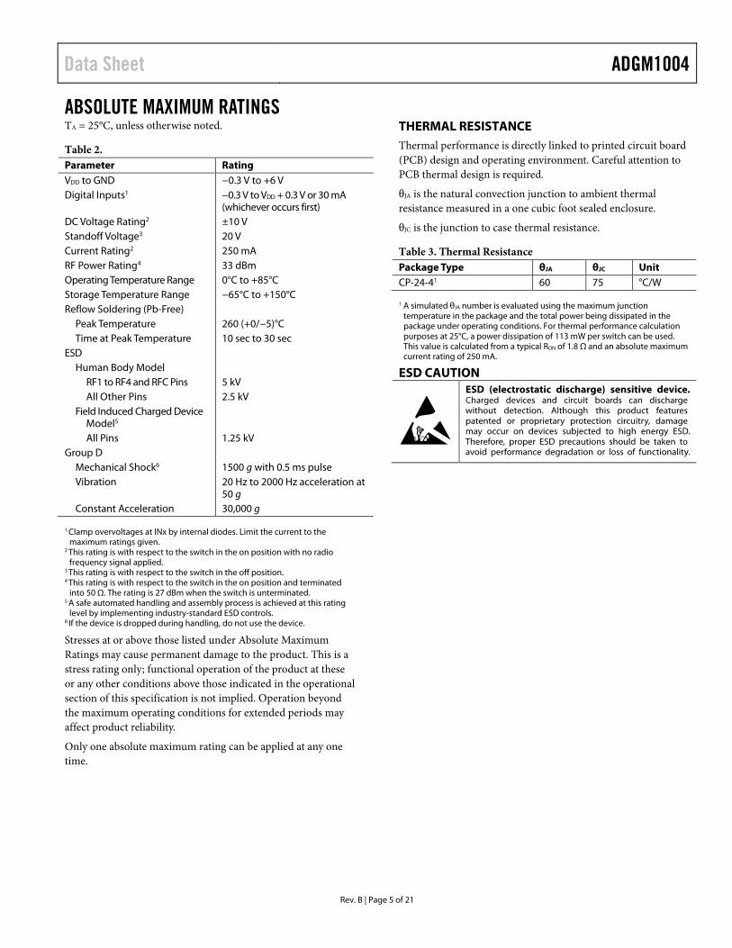
ABSOLUTE MAXIMUM RATINGS TA = 25°C, unless otherwise noted.
Table 2. Parameter Rating VDD to GND −0.3 V to +6 V Digital Inputs1 −0.3 V to VDD + 0.3 V or 30 mA
(whichever occurs first) DC Voltage Rating2 ±10 V Standoff Voltage3 20 V Current Rating2 250 mA RF Power Rating4 33 dBm Operating Temperature Range 0°C to +85°C Storage Temperature Range −65°C to +150°C Reflow Soldering (Pb-Free)
Peak Temperature 260 (+0/−5)°C Time at Peak Temperature 10 sec to 30 sec
ESD Human Body Model
RF1 to RF4 and RFC Pins 5 kV All Other Pins 2.5 kV
Field Induced Charged Device Model5
All Pins 1.25 kV Group D
Mechanical Shock6 1500 g with 0.5 ms pulse Vibration 20 Hz to 2000 Hz acceleration at
50 g Constant Acceleration 30,000 g
1 Clamp overvoltages at INx by internal diodes. Limit the current to the
maximum ratings given. 2 This rating is with respect to the switch in the on position with no radio
frequency signal applied. 3 This rating is with respect to the switch in the off position. 4 This rating is with respect to the switch in the on position and terminated
into 50 Ω. The rating is 27 dBm when the switch is unterminated. 5 A safe automated handling and assembly process is achieved at this rating
level by implementing industry-standard ESD controls. 6 If the device is dropped during handling, do not use the device.
Stresses at or above those listed under Absolute Maximum Ratings may cause permanent damage to the product. This is a stress rating only; functional operation of the product at these or any other conditions above those indicated in the operational section of this specification is not implied. Operation beyond the maximum operating conditions for extended periods may affect product reliability.
Only one absolute maximum rating can be applied at any one time.
THERMAL RESISTANCE Thermal performance is directly linked to printed circuit board (PCB) design and operating environment. Careful attention to PCB thermal design is required.
θJA is the natural convection junction to ambient thermal resistance measured in a one cubic foot sealed enclosure.
θJC is the junction to case thermal resistance.
Table 3. Thermal Resistance Package Type θJA θJC Unit CP-24-41 60 75 °C/W
1 A simulated θJA number is evaluated using the maximum junction temperature in the package and the total power being dissipated in the package under operating conditions. For thermal performance calculation purposes at 25°C, a power dissipation of 113 mW per switch can be used. This value is calculated from a typical RON of 1.8 Ω and an absolute maximum current rating of 250 mA.
ESD CAUTION
ADGM1004 Data Sheet
Rev. B | Page 6 of 21
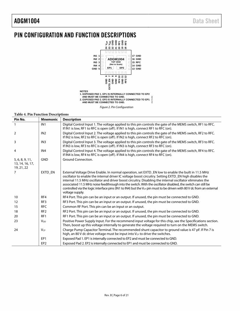
PIN CONFIGURATION AND FUNCTION DESCRIPTIONS
IN1IN2IN3IN4
EP1 EP2GND
NOTES1. EXPOSED PAD 1. EP1 IS INTERNALLY CONNECTED TO EP2
AND MUST BE CONNECTED TO GND.2. EXPOSED PAD 2. EP2 IS INTERNALLY CONNECTED TO EP1
AND MUST BE CONNECTED TO GND.
GNDGNDRFCGNDGND
12345
1716151413
GN
DEX
TD_E
NG
ND
GN
DR
F4
6 7 8 9 10G
ND
11R
F3
V CP
V DD
GN
DG
ND
RF1
GN
DR
F212
24 23 22 21 20 19 18
ADGM1004TOP VIEW
(Not to Scale)
1517
3-00
2
Figure 2. Pin Configuration
Table 4. Pin Function Descriptions Pin No. Mnemonic Description 1 IN1 Digital Control Input 1. The voltage applied to this pin controls the gate of the MEMS switch, RF1 to RFC.
If IN1 is low, RF1 to RFC is open (off ). If IN1 is high, connect RF1 to RFC (on). 2 IN2 Digital Control Input 2. The voltage applied to this pin controls the gate of the MEMS switch, RF2 to RFC.
If IN2 is low, RF2 to RFC is open (off ). If IN2 is high, connect RF2 to RFC (on). 3 IN3 Digital Control Input 3. The voltage applied to this pin controls the gate of the MEMS switch, RF3 to RFC.
If IN3 is low, RF3 to RFC is open (off ). If IN3 is high, connect RF3 to RFC (on). 4 IN4 Digital Control Input 4. The voltage applied to this pin controls the gate of the MEMS switch, RF4 to RFC.
If IN4 is low, RF4 to RFC is open (off ). If IN4 is high, connect RF4 to RFC (on). 5, 6, 8, 9, 11, 13, 14, 16, 17, 19, 21, 22
GND Ground Connection.
7 EXTD_EN External Voltage Drive Enable. In normal operation, set EXTD_EN low to enable the built in 11.5 MHz oscillator to enable the internal driver IC voltage boost circuitry. Setting EXTD_EN high disables the internal 11.5 MHz oscillator and driver boost circuitry. Disabling the internal oscillator eliminates the associated 11.5 MHz noise feedthrough into the switch. With the oscillator disabled, the switch can still be controlled via the logic interface pins (IN1 to IN4) but the VCP pin must to be driven with 80 V dc from an external voltage supply.
10 RF4 RF4 Port. This pin can be an input or an output. If unused, the pin must be connected to GND. 12 RF3 RF3 Port. This pin can be an input or an output. If unused, the pin must be connected to GND. 15 RFC Common RF Port. This pin can be an input or an output. 18 RF2 RF2 Port. This pin can be an input or an output. If unused, the pin must be connected to GND. 20 RF1 RF1 Port. This pin can be an input or an output. If unused, the pin must be connected to GND. 23 VDD Positive Power Supply Input. For the recommend input voltage for this chip, see the Specifications section.
Then, boost up this voltage internally to generate the voltage required to turn on the MEMS switch. 24 VCP Charge Pump Capacitor Terminal. The recommended shunt capacitor to ground value is 47 pF. If Pin 7 is
high, an 80 V dc drive voltage must be input into VCP to drive the switches. EP1 Exposed Pad 1. EP1 is internally connected to EP2 and must be connected to GND. EP2 Exposed Pad 2. EP2 is internally connected to EP1 and must be connected to GND.
Data Sheet ADGM1004
Rev. B | Page 7 of 21
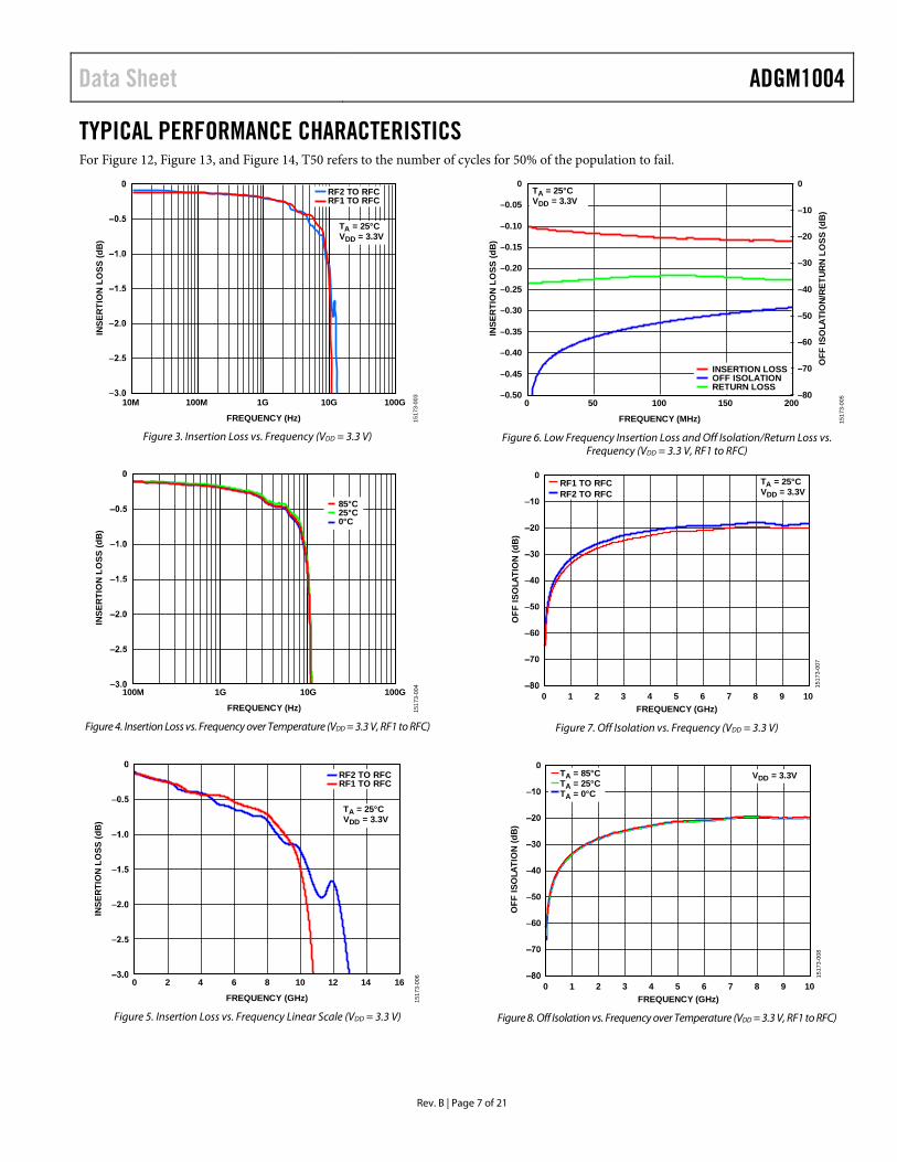
TYPICAL PERFORMANCE CHARACTERISTICS For Figure 12, Figure 13, and Figure 14, T50 refers to the number of cycles for 50% of the population to fail.
10M 100M 1G 10G 100G
INSE
RTI
ON
LO
SS (d
B)
FREQUENCY (Hz)
RF2 TO RFCRF1 TO RFC
TA = 25°CVDD = 3.3V
1517
3-00
3
Figure 3. Insertion Loss vs. Frequency (VDD = 3.3 V)
100M 1G 10G 100G
INSE
RTI
ON
LO
SS (d
B)
FREQUENCY (Hz)
85°C25°C0°C
1517
3-00
4
Figure 4. Insertion Loss vs. Frequency over Temperature (VDD = 3.3 V, RF1 to RFC)
0 2 4 6 8 10 12 14 16
INSE
RTI
ON
LO
SS (d
B)
FREQUENCY (GHz)
RF2 TO RFCRF1 TO RFC
1517
3-00
6
TA = 25°CVDD = 3.3V
Figure 5. Insertion Loss vs. Frequency Linear Scale (VDD = 3.3 V)
–80
–70
–60
–50
–40
–30
–20
–10
0
–0.50
–0.45
–0.40
–0.35
–0.30
–0.25
–0.20
–0.15
–0.10
–0.05
0
0 50 100 150 200
OFF
ISO
LATI
ON
/RET
UR
N L
OSS
(dB
)
INSE
RTI
ON
LO
SS (d
B)
FREQUENCY (MHz)
INSERTION LOSSOFF ISOLATIONRETURN LOSS
TA = 25°CVDD = 3.3V
1517
3-00
5
Figure 6. Low Frequency Insertion Loss and Off Isolation/Return Loss vs.
Frequency (VDD = 3.3 V, RF1 to RFC)
0 1 2 3 4 6 7 8 95 10
OFF
ISO
LATI
ON
(dB
)
FREQUENCY (GHz)
TA = 25°CVDD = 3.3V
RF1 TO RFCRF2 TO RFC
1517
3-00
7
Figure 7. Off Isolation vs. Frequency (VDD = 3.3 V)
OFF
ISO
LATI
ON
(dB
)
0 1 2 3 4 6 7 8 95 10FREQUENCY (GHz)
1517
3-00
8
VDD = 3.3VTA = 85°CTA = 25°CTA = 0°C
Figure 8. Off Isolation vs. Frequency over Temperature (VDD = 3.3 V, RF1 to RFC)
ADGM1004 Data Sheet
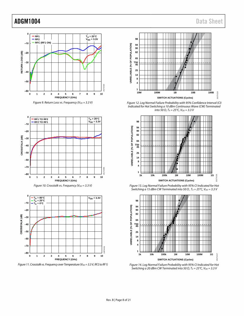
Rev. B | Page 8 of 21
0 1 2 3 4 6 7 8 95 10
RET
UR
N L
OSS
(dB
)
FREQUENCY (GHz)
TA = 25°CVDD = 3.3V
1517
3-01
0
RF1RF2RFC (RF1 ON)
Figure 9. Return Loss vs. Frequency (VDD = 3.3 V)
CR
OSS
TALK
(dB
)
0 1 2 3 4 6 7 8 95 10FREQUENCY (GHz)
1517
3-00
9
TA = 25°CVDD = 3.3V
RF1 TO RF2RF2 TO RF1
Figure 10. Crosstalk vs. Frequency (VDD = 3.3 V)
0 1 2 3 4 6 7 8 95 10FREQUENCY (GHz)
1287
4-01
1
VDD = 3.3VTA = 85°CTA = 25°CTA = 0°C
Figure 11. Crosstalk vs. Frequency over Temperature (VDD = 3.3 V, RF2 to RF1)
10M 100M 1B
SWITCH ACTUATIONS (Cycles)
UN
REL
IAB
LE (%
OF
POPU
LATI
ON
)
10B 100B
98
949082
65T50
45
25
148
4
1
1517
3-21
5
Figure 12. Log Normal Failure Probability with 95% Confidence Interval (CI) Indicated for Hot Switching a 10 dBm Continuous Wave (CW) Terminated
into 50 Ω, TA = 25°C, VDD = 3.3 V
1k 10k 100k 1M 10M
SWITCH ACTUATIONS (Cycles)
UN
REL
IAB
LE (%
OF
POPU
LATI
ON
)
100M 1G
98
949082
65T50
45
25
148
4
1
1517
3-21
6
Figure 13. Log Normal Failure Probability with 95% CI Indicated for Hot
Switching a 15 dBm CW Terminated into 50 Ω , TA = 25°C, VDD = 3.3 V
SWITCH ACTUATIONS (Cycles)
UN
REL
IAB
LE (%
OF
POPU
LATI
ON
)
98
949082
65T50
45
25
148
4
1
1517
3-21
71k 10k 100k 1M 10M 100M 1G
Figure 14. Log Normal Failure Probability with 95% CI Indicated for Hot
Switching a 20 dBm CW Terminated into 50 Ω, TA = 25°C, VDD = 3.3 V
Data Sheet ADGM1004
Rev. B | Page 9 of 21
–120
–100
–80
–60
–40
–20
0
0 2 4 6 8 10 12
THD
+ N
(dB
c)
SIGNAL AMPLITUDE (V p-p)
100Hz1kHz5kHz
1517
3-01
2
Figure 15. Total Harmonic Distortion Plus Noise (THD + N) vs. Signal
Amplitude (VDD = 3.3 V) RLOAD = 300 Ω, TA = 25°C)
–1.0
–0.8
–0.6
–0.4
–0.2
0
0.2
0.4
0.6
0.8
1.0
–0.5
0
0.5
1.0
1.5
2.0
2.5
3.0
3.5
0 10 20 30 40
TEST
SIG
NAL
(V)
DIG
ITA
L C
ON
TRO
L SI
GN
AL
(V)
TIME (µs) 1517
3-01
4
DIGITAL CONTROLtON/tOFF TEST SIGNAL
TA = 25°CVDD = 3.3V
Figure 16. Digital Control Signal and Test Signal vs. Time (VDD = 3.3 V)
–0.20
–0.18
–0.16
–0.14
–0.12
–0.10
–0.08
–0.06
–0.04
–0.02
0
0 0.01 0.02 0.03 0.04 0.05 0.06 0.07 0.08 0.09 0.10
RO
N VA
RIA
TIO
N (Ω
)
TIME (Seconds)
TA = 0°CTA = 25°CTA = 85°C
1517
3-21
8
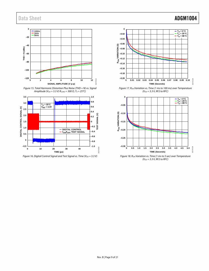
Figure 17. RON Variation vs. Time (1 ms to 100 ms) over Temperature
(VDD = 3.3 V, RF2 to RFC)
–0.30
–0.25
–0.20
–0.15
–0.10
–0.05
0
0 0.5 1.0 1.5 2.0 2.5 3.0 3.5 4.0 4.5 5.0
RO
N V
AR
IATI
ON
(Ω)
TIME (Seconds) 1517
3-21
9
TA = 0°CTA = 25°CTA = 85°C
Figure 18. RON Variation vs. Time (1 ms to 5 sec) over Temperature
(VDD = 3.3 V, RF2 to RFC)
ADGM1004 Data Sheet
Rev. B | Page 10 of 21
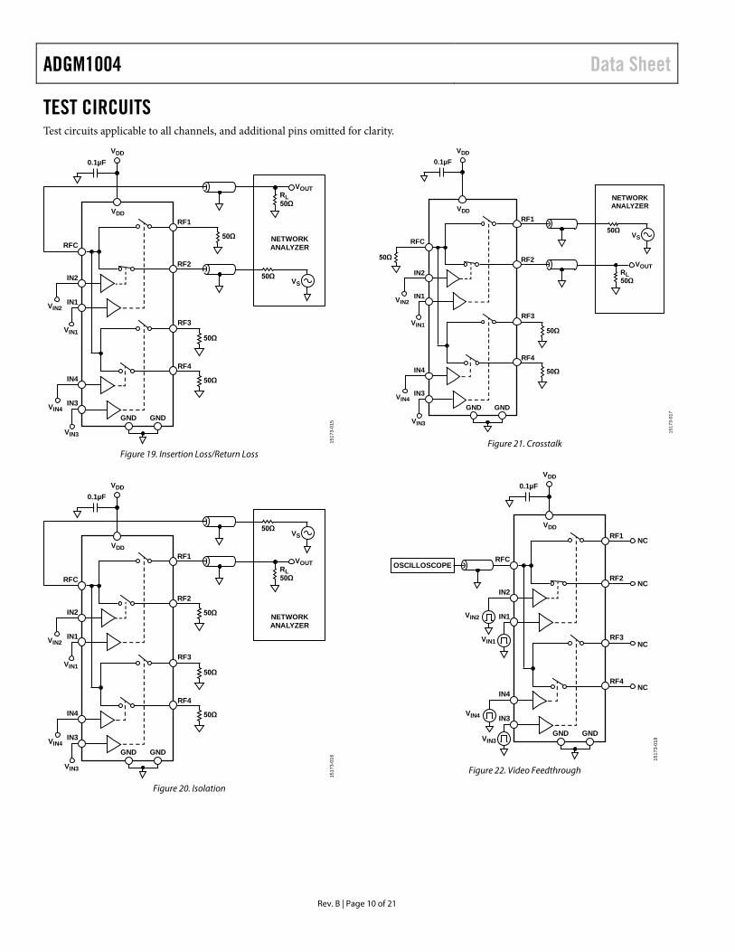
TEST CIRCUITS Test circuits applicable to all channels, and additional pins omitted for clarity.
VS50Ω
VOUTRL50Ω
VIN2
VDD
0.1µFVDD
RF2
RF1
IN2
RFC
VIN1RF3
50Ω
IN1
50Ω
50Ω
RF4
VIN4
IN4
VIN3
IN3
GNDGND
1517
3-01
5
NETWORKANALYZER
Figure 19. Insertion Loss/Return Loss
VS
NETWORKANALYZER
50Ω
VOUTRL50Ω
VIN2
VDD
0.1µFVDD
RF2
RF1
IN2
RFC
VIN1RF3
50Ω
IN1
50Ω
RF4
VIN4
IN4
VIN3
IN3
50Ω
1517
3-01
6GNDGND
Figure 20. Isolation
VIN2
VDD
0.1µFVDD
RF2
RF1
IN2
RFC
VIN1RF3
50Ω
IN1
50Ω
50Ω
RF4
VIN4
IN4
VIN3
IN3
1517
3-01
7
VS
NETWORKANALYZER
50Ω
VOUTRL50Ω
GNDGND
Figure 21. Crosstalk
VIN2
VDD
0.1µFVDD
RF2
RF1
IN2
NC
NC
NC
NC
RFCOSCILLOSCOPE
VIN1 RF3
IN1
RF4
VIN4
IN4
VIN3
IN3
1517
3-01
8
GNDGND
Figure 22. Video Feedthrough
Data Sheet ADGM1004
Rev. B | Page 11 of 21
0.1µF
VIN2
VDD
VDD
RF1
RF2
IN2
RFC
VIN1
RF3
50Ω
IN1
50Ω
50Ω
RF4
VIN4
IN4
VIN3
IN315
173-
019
SPECTRUMANALYZER
COMBINERNETWORK
RFSOURCE
RFSOURCE
GNDGND
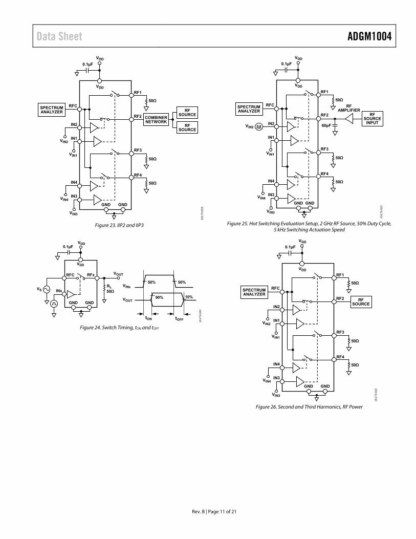
Figure 23. IIP2 and IIP3
tON
50% 50%
90% 10%
VINx
VOUT
tOFF
VDD
VDD
0.1µF
VS INx
RFxRFC
RL50Ω
VOUT
1517
3-02
0
GNDGND
Figure 24. Switch Timing, tON and tOFF
0.1µF
VIN2
VDD
RF1
RF2
60pFIN2
RFC
VIN1
RF3
50Ω
IN1
50Ω
50Ω
RF4
VIN4
IN4
VIN3
IN3
1517
3-02
1
SPECTRUMANALYZER
RFSOURCE
INPUT
RFAMPLIFIER
VDD
GNDGND
Figure 25. Hot Switching Evaluation Setup, 2 GHz RF Source, 50% Duty Cycle, 5 kHz Switching Actuation Speed
0.1µF
VIN2
VDD
VDD
RF1
RF2
IN2
RFC
VIN1
RF3
50Ω
IN1
50Ω
50Ω
RF4
VIN4
IN4
VIN3
IN315
173-
022
SPECTRUMANALYZER
RFSOURCE
GNDGND
Figure 26. Second and Third Harmonics, RF Power
ADGM1004 Data Sheet
Rev. B | Page 12 of 21
VDD
VDD
0.1µF
VINx
INx
RFxRFC
AGNDRFGND
V
1517
3-22
7
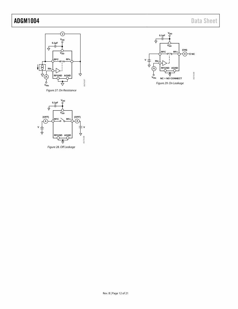
Figure 27. On Resistance
1517
3-22
8
VDD
VDD
0.1µF
V
RFxRFC
AGNDRFGND
AA
V
(OFF) (OFF)
Figure 28. Off Leakage
1517
3-22
9
VDD
NC
VDD
0.1µF
V
VINx
INx
RFxRFC
AGNDRFGND
A(ON)
NC = NO CONNECT Figure 29. On Leakage
Data Sheet ADGM1004
Rev. B | Page 13 of 21
TERMINOLOGY Insertion Loss (IL) IL is the amount of signal attenuation between the input and output ports of the switch when the switch is in the on state. Expressed in decibels, ensure that insertion loss is as small as possible for maximum power transfer.
An example calculation of insertion loss based on the setup in Figure 19 is as follows:
IL (dB) = −20log10|SRF2RFC|
where SRF2RFC is the transmission coefficient measured from RF2 to RFC with RF2 in the on position. All unused switches are in the off position and terminated in a purely resistive load of 50 Ω.
Isolation (ISO) ISO is the amount of signal attenuation between the input and output ports of the switch when the switch is in the off state. Expressed in decibels, ensure that isolation is as large as possible.
An example calculation of isolation based on the setup in Figure 20 is as follows:
ISO (dB) = −20log10|SRFCRF1|
Where SRFCRF1 is the transmission coefficient measured from RFC to RF1 with RF1 in the off position. All unused switches are in the off position and terminated in a purely resistive load of 50 Ω.
Crosstalk (CTK) CTK is a measure of unwanted signals coupled through from one channel to another because of parasitic capacitance.
An example calculation of crosstalk based on the setup in Figure 21 is as follows:
CTK (dB) = −20log10|SRF1RF2|
where SRF1RF2 is the transmission coefficient measured from RF1 to RF2 with RF1 in the off position and RF2 in the on position. All unused switches are in the off position and terminated in a purely resistive load of 50 Ω.
Return Loss (RL) RL is the magnitude of the reflection coefficient expressed in decibels, and the amount of reflected signal relative to the incident signal.
An example calculation of return loss based on the setup in Figure 19 is as follows:
RL (dB) = −20log10|S11|
where S11 is the reflection coefficient of the port under test.
Third-Order Intermodulation Intercept (IIP3) IIP3 is the intersection point of the fundamental POUT vs. PIN extrapolated line and the third-order intermodulation products extrapolated line of a two-tone test. IIP3 is a figure of merit that characterizes the switch linearity.
Second-Order Intermodulation Intercept (IIP2) IIP2 is the intersection point of the fundamental POUT vs. PIN extrapolated line and the second-order intermodulation products extrapolated line of a two-tone test. IIP2 is a figure of merit that characterizes the switch linearity.
Second Harmonic (HD2) HD2 is the amplitude of the second harmonic, where, for a signal whose fundamental frequency is f, the second harmonic has a frequency of 2 f. This measurement is a single-tone test, expressed with reference to the carrier signal (dBc).
Third Harmonic (HD3) HD3 is the amplitude of the third harmonic, where, for a signal whose fundamental frequency is f, the third harmonic has a frequency of 3 f. This measurement is a single tone test, expressed with reference to the carrier signal (dBc).
On Switching Time (tON) tON is the time it takes for the switch to turn on. It is measured from 50% of the control signal (INx) to 90% of the on level. No power was applied through the switch during this test (cold switched). The switch was terminated into a 50 Ω load.
Off Switching Time (tOFF) tOFF is the time it takes for the switch to turn off. It is measured from 50% of the control signal (INx) to 10% of the on level. No power was applied through the switch during this test (cold switched). The switch was terminated into a 50 Ω load.
Settling Time Rising Edge The settling time rising edge is the time it takes for the power of an RF signal to settle within 0.05 dB of its final steady state value. The switch was terminated into a 50 Ω load.
Settling Time Falling Edge The settling time falling edge is the time it takes for the power of an RF signal to settle within 0.05 dB of its final steady state value. The switch was terminated into a 50 Ω load.
Actuation Frequency The actuation frequency refers to the speed at which the ADGM1004 can be switched on and off. Actuation frequency is dependent on both settling times and on/off switching times.
Power-Up Time The power-up time is a measure of the time required for the device to power up and start to pass 90% of an RF input signal after VDD has reached 95%.
Video Feedthrough Video feedthrough is a measure of the spurious signals present at the RFx ports of the switch when the control voltage is switched from high to low or from low to high without an RF signal present.
Internal Oscillator Frequency The internal oscillator frequency is the value of the on-board oscillator that drives the gate control chip of the ADGM1004.
ADGM1004 Data Sheet
Rev. B | Page 14 of 21
Internal Oscillator Feedthrough The internal oscillator feedthrough is the amount of internal oscillator signal that feeds through to the RFx and RFC pins of the switch. This signal appears as a noise spur on the RFx and RFC pins of the switch at the frequency the oscillator is operating at and harmonics thereof.
On Resistance (RON) RON is the resistance of a switch in the closed/on state measured between the package pins. Measure resistance in 4-wire mode to null out any cabling or PCB series resistances.
On Resistance Variation On resistance variation is the variation in the on resistance of the switch over the specified criteria in Table 1.
Continuously On Lifetime The continuously on lifetime parameter measures how long the switch is left in a continuously on state. If the switch is left in the on position for an extended period, it affects the turn off mechanism of the device.
Actuation Lifetime Actuation lifetime is the number of consecutive open/close/ open cycles that can complete without the on resistance exceeding a specified limit and no occurrence of failures to open (FTO) or failures to close (FTC).
Cold Switching Cold switching operates the switch in a mode so that no voltage differential exists between source and drain when the switch is closed and/or no current is flowing source to drain when the switch opens. All switches have longer lives when cold switched.
Hot Switching Hot switching is operating the switch in a mode where a voltage differential exists between source and drain when the switch is closed and/or current is flowing RFx to RFC when the switch is opened. Hot switching results in a reduced switch life, depending on the magnitude of the open circuit voltage between the source and the drain.
Input High Voltage (VINH) VINH is the minimum input voltage for Logic 1.
Input Low Voltage (VINL) VINL is the maximum input voltage for Logic 0.
Data Sheet ADGM1004
Rev. B | Page 15 of 21
THEORY OF OPERATION The ADGM1004 is a wideband SP4T switch fabricated using Analog Devices, Inc., MEMS switch technology. This technology enables high power, low loss, low distortion gigahertz switches to be realized for demanding RF applications.
A key strength of the MEMS switch is that it simultaneously brings together best-in-class high frequency RF performance and 0 Hz/dc precision performance. This combination coupled with superior reliability and a tiny surface mountable form factor make the MEMS switch the ideal switching solution for all RF and precision signal instrumentation needs.
Figure 30 shows a stylized cross section graphic of the switch with dimensions. The switch is an electrostatically actuated cantilever beam connected in a 3-terminal configuration. Functionally, it is analogous to a field effect transistor (FET); the terminals can be used as a source, gate, and drain.
SILICON
SILICON CAP
SOURCE DRAINCANTILEVER BEAM
GATE CONTACT GAPMETAL
1517
3-12
6
Figure 30. Cross Section of the MEMS Switch Design Showing the Cantilever
Switch Beam (Not to Scale)
When a dc actuation voltage is applied between the gate electrode and the source (the switch beam), an electrostatic force is generated, resulting in attracting the beam toward the substrate. A separate on-board charge pump IC generates the bias voltage; 80 V is used for actuation.
When the bias voltage between the gate and the source exceeds the threshold voltage of the switch, VTH, the contacts on the beam touch the drain, which completes the circuit between the source and the drain and turns the switch on. When the bias voltage is removed, that is, 0 V on the gate electrode, the beam acts as a spring generating a sufficient restoring force to open the connection between the source and the drain, thus breaking the circuit and turning the switch off.
The silicon cap covering the switch die is shown in Figure 30. This cap hermetically seals the switch, which improves reliability. The switch contacts do not suffer from dry switching or low power switching lifetime degradation.
DIGITAL INTERFACE The ADGM1004 is controlled via a parallel interface. Standard CMOS/LVTTL signals applied through this interface control the actuation or release of all of the switch channels of the ADGM1004. Gate signals applied are boosted to provide the required voltages needed to actuate the MEMS switch.
Pin 1 to Pin 4 (IN1 to IN4) control the switching functions of the ADGM1004. When a Logic 1 is applied to one of these pins, the gate of the corresponding switch is activated, and the switch turns on. Conversely, when a Logic 0 is applied to any of these pins, the switch turns off. Note that it is possible to connect more than one RFx input to RFC at a time. The truth table for the ADGM1004 is given in Table 5.
Table 5. Truth Table IN1 IN2 IN3 IN4 RF1 to RFC RF2 to RFC RF3 to RFC RF4 to RFC 0 0 0 0 Off Off Off Off 0 0 0 1 Off Off Off On 0 0 1 0 Off Off On Off 0 0 1 1 Off Off On On 0 1 0 0 Off On Off Off 0 1 0 1 Off On Off On 0 1 1 0 Off On On Off 0 1 1 1 Off On On On 1 0 0 0 On Off Off Off 1 0 0 1 On Off Off On 1 0 1 0 On Off On Off 1 0 1 1 On Off On On 1 1 0 0 On On Off Off 1 1 0 1 On On Off On 1 1 1 0 On On On Off 1 1 1 1 On On On On
ADGM1004 Data Sheet
Rev. B | Page 16 of 21
INTERNAL OSCILLATOR/EXTD_EN The ADGM1004 has an internal oscillator running at a nominal 11.5 MHz. This oscillator drives the charge pump circuitry that provides the actuation voltage for each of the switch gate elec-trodes. Although this oscillator is very low power, the 11.5 MHz signal is coupled to the switch and can be considered a noise spur on the switch channels. The magnitude of this feedthrough noise spur is specified in Table 1 and is typically −115 dBm when one switch is on. When all four switches are simultaneously on, the feedthrough goes up to −94 dBm. VDD level and temperature changes affect the frequency of the noise spur. For the maximum and minimum frequency range over temperature and voltage supply range, see Table 1.
Setting the EXTD_EN pin high disables the internal oscillator and driver boost circuitry. With the driver boost circuitry disabled, applying an external 80 V dc to the VCP pin enables the switch to be driven via the digital interface, as outlined in Table 4. Disabling the boost circuitry and driving it with an external 80 V dc source completely eliminates oscillator feedthrough that can be an issue in some applications.
TYPICAL OPERATING CIRCUIT Figure 31 shows the typical operating circuit for the ADGM1004 as used in the EVAL-ADGM1004EBZ evaluation board. A 47 pF external capacitor is required on the VCP pin; this capacitor is a holding capacitor for the 80 V dc gate drive voltage. Because the device incorporates the boost circuitry required to generate the 80 V dc, the boost circuitry results in an overall saving in the number of external components required, and therefore reduces board space needed to use the device.
In the circuit shown in Figure 31, VDD is connected to 3.3 V. EP1 connects to EP2 internally. Typically, one large GND pad on the PCB is used to short together EP1 and EP2. Figure 31 shows the ADGM1004 configured to use the internal oscillator as the reference clock to the driver IC control circuit. Alternatively, set Pin 7 high and apply 80 V dc directly to Pin 24 to disable the internal oscillator and eliminate all oscillator feedthrough. The switches can then be controlled as normal via the logic control interface, Pin 1 to Pin 4.
GND
GND
GND
GND
RFC
24
GN
D
EXTD
_EN
GN
D
RF3
RF2
GN
D
GN
D
RF1
23 22 21 20 19 18
1
2
3
4
5
6 7 8 9 10 11 12
17
16
15
14
13
IN1
IN2
IN3
IN4
GND
GN
D
RF4 GN
D
V CP
V DD
GN
D
IN1
IN2
IN3
IN4
47pF
0.1µF
3.3V
RFOUT
RF2
IN
RF1
INR
F4 IN
RF3
IN
EP1 EP2
TOP VIEW
1517
3-02
3
Figure 31. Typical Operating Circuit
Data Sheet ADGM1004
Rev. B | Page 17 of 21
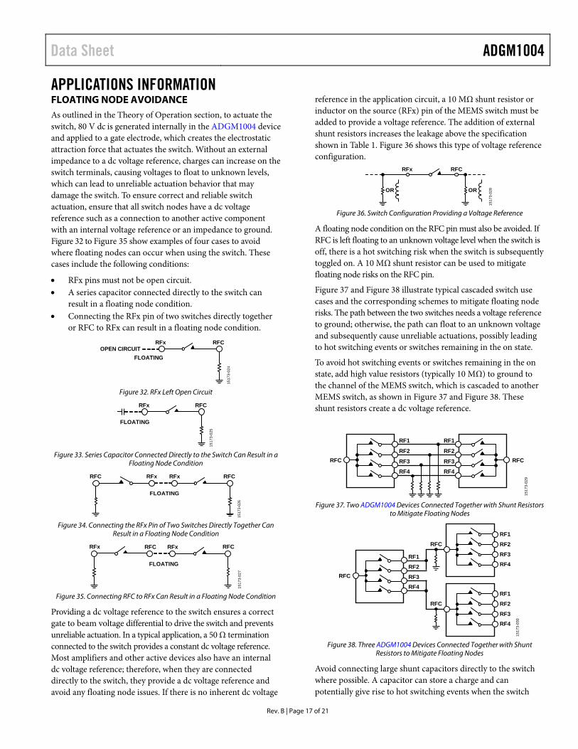
APPLICATIONS INFORMATION FLOATING NODE AVOIDANCE As outlined in the Theory of Operation section, to actuate the switch, 80 V dc is generated internally in the ADGM1004 device and applied to a gate electrode, which creates the electrostatic attraction force that actuates the switch. Without an external impedance to a dc voltage reference, charges can increase on the switch terminals, causing voltages to float to unknown levels, which can lead to unreliable actuation behavior that may damage the switch. To ensure correct and reliable switch actuation, ensure that all switch nodes have a dc voltage reference such as a connection to another active component with an internal voltage reference or an impedance to ground. Figure 32 to Figure 35 show examples of four cases to avoid where floating nodes can occur when using the switch. These cases include the following conditions:
• RFx pins must not be open circuit. • A series capacitor connected directly to the switch can
result in a floating node condition. • Connecting the RFx pin of two switches directly together
or RFC to RFx can result in a floating node condition. RFx RFC
FLOATINGOPEN CIRCUIT
1517
3-02
4
Figure 32. RFx Left Open Circuit
RFx RFC
FLOATING
1517
3-02
5
Figure 33. Series Capacitor Connected Directly to the Switch Can Result in a
Floating Node Condition
RFx RFC
FLOATING
RFxRFC
1517
3-02
6
Figure 34. Connecting the RFx Pin of Two Switches Directly Together Can
Result in a Floating Node Condition
RFx RFC
FLOATING
RFCRFx
1517
3-02
7
Figure 35. Connecting RFC to RFx Can Result in a Floating Node Condition
Providing a dc voltage reference to the switch ensures a correct gate to beam voltage differential to drive the switch and prevents unreliable actuation. In a typical application, a 50 Ω termination connected to the switch provides a constant dc voltage reference. Most amplifiers and other active devices also have an internal dc voltage reference; therefore, when they are connected directly to the switch, they provide a dc voltage reference and avoid any floating node issues. If there is no inherent dc voltage
reference in the application circuit, a 10 MΩ shunt resistor or inductor on the source (RFx) pin of the MEMS switch must be added to provide a voltage reference. The addition of external shunt resistors increases the leakage above the specification shown in Table 1. Figure 36 shows this type of voltage reference configuration.
RFx
OR OR
RFC
1517
3-02
8
Figure 36. Switch Configuration Providing a Voltage Reference
A floating node condition on the RFC pin must also be avoided. If RFC is left floating to an unknown voltage level when the switch is off, there is a hot switching risk when the switch is subsequently toggled on. A 10 MΩ shunt resistor can be used to mitigate floating node risks on the RFC pin.
Figure 37 and Figure 38 illustrate typical cascaded switch use cases and the corresponding schemes to mitigate floating node risks. The path between the two switches needs a voltage reference to ground; otherwise, the path can float to an unknown voltage and subsequently cause unreliable actuations, possibly leading to hot switching events or switches remaining in the on state.
To avoid hot switching events or switches remaining in the on state, add high value resistors (typically 10 MΩ) to ground to the channel of the MEMS switch, which is cascaded to another MEMS switch, as shown in Figure 37 and Figure 38. These shunt resistors create a dc voltage reference.
RFC
RF1
RF2
RF3
RF4
RF1
RF2
RF3
RF4
RFC
1517
3-02
9
Figure 37. Two ADGM1004 Devices Connected Together with Shunt Resistors
to Mitigate Floating Nodes
RFC
RF1
RF2
RF3
RF4
RFC
RF1
RF2
RF3
RF4
RFC
RF1
RF2
RF3
RF4
1517
3-03
0
Figure 38. Three ADGM1004 Devices Connected Together with Shunt
Resistors to Mitigate Floating Nodes
Avoid connecting large shunt capacitors directly to the switch where possible. A capacitor can store a charge and can potentially give rise to hot switching events when the switch
ADGM1004 Data Sheet
Rev. B | Page 18 of 21
opens or closes where there are no alternative discharge paths, which affects the cycle lifetime of the switch.
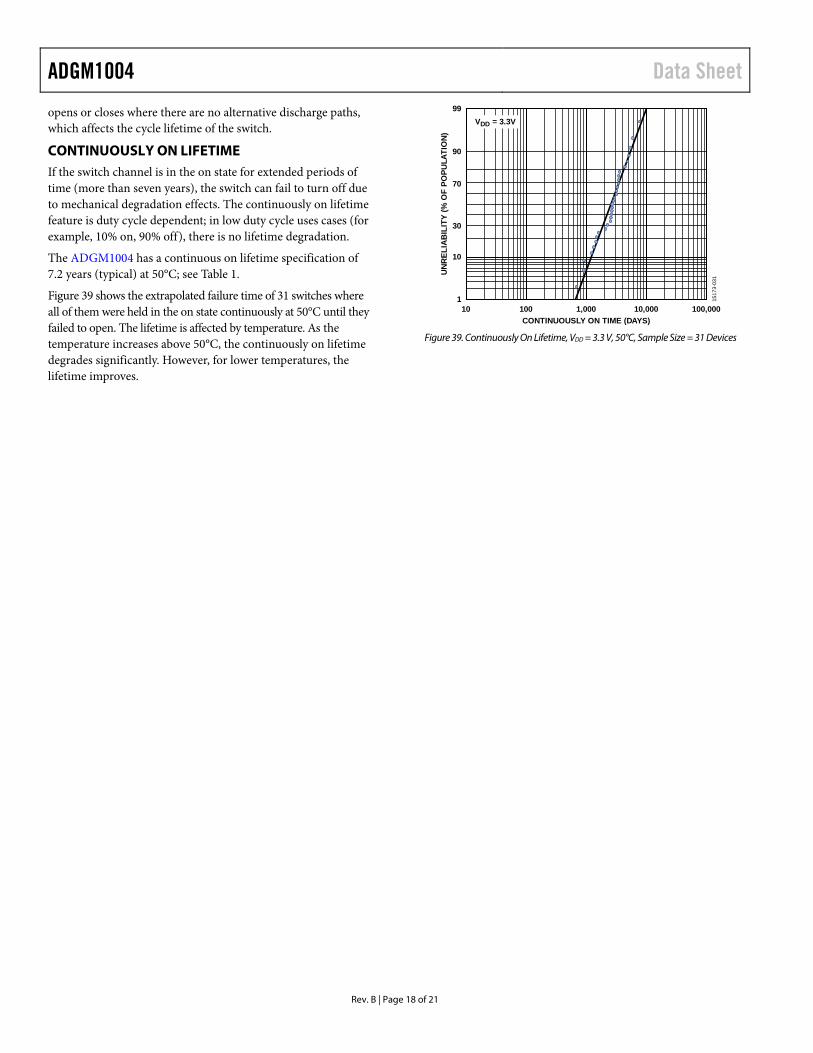
CONTINUOUSLY ON LIFETIME If the switch channel is in the on state for extended periods of time (more than seven years), the switch can fail to turn off due to mechanical degradation effects. The continuously on lifetime feature is duty cycle dependent; in low duty cycle uses cases (for example, 10% on, 90% off), there is no lifetime degradation.
The ADGM1004 has a continuous on lifetime specification of 7.2 years (typical) at 50°C; see Table 1.
Figure 39 shows the extrapolated failure time of 31 switches where all of them were held in the on state continuously at 50°C until they failed to open. The lifetime is affected by temperature. As the temperature increases above 50°C, the continuously on lifetime degrades significantly. However, for lower temperatures, the lifetime improves.
99
90
70
UN
REL
IAB
ILIT
Y (%
OF
POPU
LATI
ON
)
30
10
110 100 1,000
CONTINUOUSLY ON TIME (DAYS)10,000 100,000
1517
3-03
1
VDD = 3.3V
Figure 39. Continuously On Lifetime, VDD = 3.3 V, 50°C, Sample Size = 31 Devices
Data Sheet ADGM1004
Rev. B | Page 19 of 21
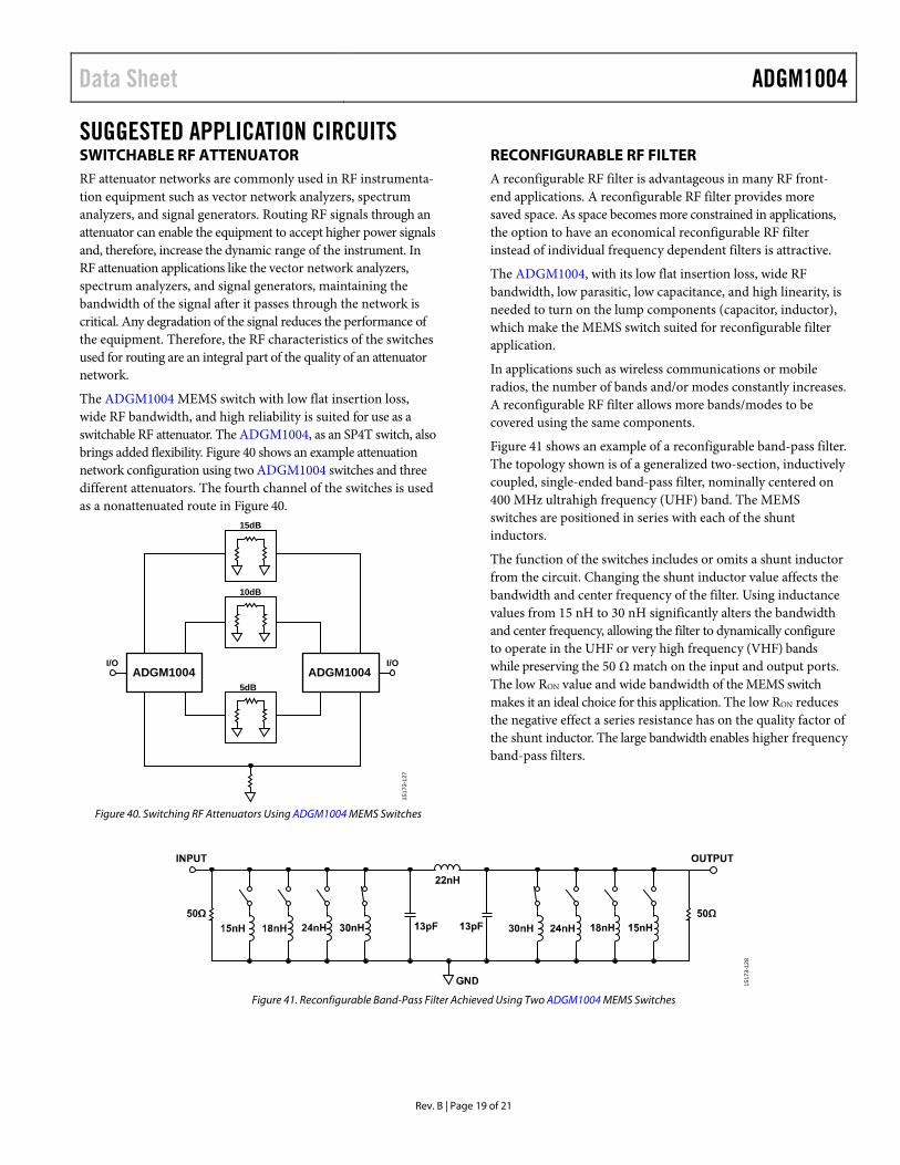
SUGGESTED APPLICATION CIRCUITS SWITCHABLE RF ATTENUATOR RF attenuator networks are commonly used in RF instrumenta-tion equipment such as vector network analyzers, spectrum analyzers, and signal generators. Routing RF signals through an attenuator can enable the equipment to accept higher power signals and, therefore, increase the dynamic range of the instrument. In RF attenuation applications like the vector network analyzers, spectrum analyzers, and signal generators, maintaining the bandwidth of the signal after it passes through the network is critical. Any degradation of the signal reduces the performance of the equipment. Therefore, the RF characteristics of the switches used for routing are an integral part of the quality of an attenuator network.
The ADGM1004 MEMS switch with low flat insertion loss, wide RF bandwidth, and high reliability is suited for use as a switchable RF attenuator. The ADGM1004, as an SP4T switch, also brings added flexibility. Figure 40 shows an example attenuation network configuration using two ADGM1004 switches and three different attenuators. The fourth channel of the switches is used as a nonattenuated route in Figure 40.
15dB
10dB
I/OADGM1004
5dB
I/OADGM1004
1517
3-12
7
Figure 40. Switching RF Attenuators Using ADGM1004 MEMS Switches
RECONFIGURABLE RF FILTER A reconfigurable RF filter is advantageous in many RF front-end applications. A reconfigurable RF filter provides more saved space. As space becomes more constrained in applications, the option to have an economical reconfigurable RF filter instead of individual frequency dependent filters is attractive.
The ADGM1004, with its low flat insertion loss, wide RF bandwidth, low parasitic, low capacitance, and high linearity, is needed to turn on the lump components (capacitor, inductor), which make the MEMS switch suited for reconfigurable filter application.
In applications such as wireless communications or mobile radios, the number of bands and/or modes constantly increases. A reconfigurable RF filter allows more bands/modes to be covered using the same components.
Figure 41 shows an example of a reconfigurable band-pass filter. The topology shown is of a generalized two-section, inductively coupled, single-ended band-pass filter, nominally centered on 400 MHz ultrahigh frequency (UHF) band. The MEMS switches are positioned in series with each of the shunt inductors.
The function of the switches includes or omits a shunt inductor from the circuit. Changing the shunt inductor value affects the bandwidth and center frequency of the filter. Using inductance values from 15 nH to 30 nH significantly alters the bandwidth and center frequency, allowing the filter to dynamically configure to operate in the UHF or very high frequency (VHF) bands while preserving the 50 Ω match on the input and output ports. The low RON value and wide bandwidth of the MEMS switch makes it an ideal choice for this application. The low RON reduces the negative effect a series resistance has on the quality factor of the shunt inductor. The large bandwidth enables higher frequency band-pass filters.
1517
3-12
8
Figure 41. Reconfigurable Band-Pass Filter Achieved Using Two ADGM1004 MEMS Switches
ADGM1004 Data Sheet
Rev. B | Page 20 of 21
HANDLING GUIDELINES ELECTRICAL OVERSTRESS (EOS) PRECAUTIONS A stored charge inadvertently conducted through the switches can result in immediate permanent damage to the ADGM1004. Therefore, observe the following precautions:
Treat the ADGM1004 as a static sensitive device and observe all normal handling precautions, which include, working only on static dissipative surfaces, wearing wrist straps or other ESD control devices, and storing unused devices in conductive foam.
Avoid connecting large capacitive terminations directly to the switch. A shunt capacitor can store a charge that can potentially give rise to hot switching events when the switch opens or closes, affecting the lifetime of the switch. Figure 42 shows where to avoid large capacitive terminations.
RFx RFC
1517
3-03
2
Figure 42. Avoid Connecting Large Capacitive Terminations Directly to the
Switch
DC VOLTAGE RANGE The dc voltage range of the switch, the dc signal range the switch is specified to carry, is ±6 V (see Table 1)
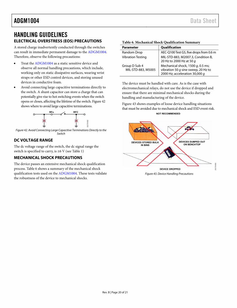
MECHANICAL SHOCK PRECAUTIONS The device passes an extensive mechanical shock qualification process. Table 6 shows a summary of the mechanical shock qualification tests used on the ADGM1004. These tests validate the robustness of the device to mechanical shocks.
Table 6. Mechanical Shock Qualification Summary Parameter Qualification Random Drop AEC-Q100 Test G5, five drops from 0.6 m Vibration Testing MIL-STD-883, M2007.3, Condition B,
20 Hz to 2000 Hz at 50 g Group D Sub 4
MIL-STD-883, M5005 Mechanical shock, 1500 g, 0.5 ms; vibration 50 g sine sweep, 20 Hz to 2000 Hz; acceleration 30,000 g
The device must be handled with care. As is the case with electromechanical relays, do not use the device if dropped and ensure that there are minimal mechanical shocks during the handling and manufacturing of the device.
Figure 43 shows examples of loose device handling situations that must be avoided due to mechanical shock and ESD event risk.
NOT RECOMMENDED
DEVICES STORED BULKIN BINS
DEVICE DROPPED
DEVICES DUMPED OUTON BENCHTOP
1517
3-03
3
Figure 43. Device Handling Precautions
Data Sheet ADGM1004
Rev. B | Page 21 of 21
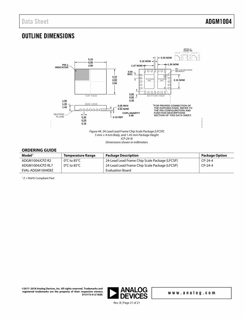
OUTLINE DIMENSIONS
*EXPOSEDPAD
*EXPOSEDPAD
BOTTOM VIEWTOP VIEW
SIDE VIEW
1
5
612
13
17
18 24
2.15 NOM
1.47 NOM
0.16 NOM0.33 NOM
1.30 NOM
1.501.451.40
0.300.250.18
0.05 MAX0.02 NOM
0.15 REFCOPLANARITY
0.08
PIN 1INDICATOR
0.650.550.45
*FOR PROPER CONNECTION OFTHE EXPOSED PADS, REFER TOTHE PIN CONFIGURATION ANDFUNCTION DESCRIPTIONSSECTION OF THIS DATA SHEET.
0.50BSC
02-0
2-20
17-A
5.105.004.90
4.104.003.90
PKG
-005
132
SEATINGPLANE
PIN 1INDIC ATOR AREA OPTIONS(SEE DETAIL A)
DETAIL A(JEDEC 95)
Figure 44. 24-Lead Lead Frame Chip Scale Package [LFCSP]
5 mm × 4 mm Body, and 1.45 mm Package Height (CP-24-4)
Dimensions shown in millimeters
ORDERING GUIDE Model1 Temperature Range Package Description Package Option ADGM1004JCPZ-R2 0°C to 85°C 24-Lead Lead Frame Chip Scale Package [LFCSP] CP-24-4 ADGM1004JCPZ-RL7 0°C to 85°C 24-Lead Lead Frame Chip Scale Package [LFCSP] CP-24-4 EVAL-ADGM1004EBZ Evaluation Board 1 Z = RoHS Compliant Part.
©2017–2018 Analog Devices, Inc. All rights reserved. Trademarks and registered trademarks are the property of their respective owners. D15173-0-3/18(B)


![D61 Evaluation of existing test methods...(HBM) ESD test [1]. And the number of ultrasensitive devices with ESD withstand voltages below 100 V is increasing (including magnetoresistive](https://img.pdfslide.net/doc/110x75/60563dade495627e0479807d/d61-evaluation-of-existing-test-methods-hbm-esd-test-1-and-the-number-of.jpg)


![dev10 ESD.ppt [호환 모드]bandi.chungbuk.ac.kr/~ysk/devnot10.pdf · 2011-07-27 · ESD Test Methods Human Body Model (HBM) Representative of an ESD event between a Human and an](https://img.pdfslide.net/doc/110x75/5f214945d7fba54739269773/dev10-esdppt-eeoebandi-yskdevnot10pdf-2011-07-27-esd-test-methods.jpg)