Embed Size (px)
Citation preview

ComponentsCatalogue
2
Contents
Continued on next page
AUTOMOTIVE RELAYS 274 - 313
Selection Guide 274 - 277
G8N-1 278 - 282
G8ND-2 283 - 287
G8NW 288 - 292
G8QN 293 - 294
G8SN 295 - 296
G8SE 297 - 298
G8HN-J 299 - 304
G8HL 305 - 309
G8JN 310 - 311
G8JR 312 - 313
SOLID STATE RELAYS 314 - 347
Technical Information 314 - 318
Selection Guide 319 - 323
G3R/G3RD 324 - 327
G3M 328 - 331
G3MB 332 - 334
G3MC 335 - 339
G3S/G3SD 340 - 343
G3DZ 344 - 347
MOSFET RELAYS 348 - 433
Technical Information 348 - 351
Selection Guide 352 - 357
G3VM-61A1/D 358 - 359
G3VM-2(F)L 360 - 361
G3VM-351A/D 362 - 363
G3VM-353A/D 364 - 365
G3VM-401A/D 366 - 367
G3VM-61G1 368 - 369
G3VM-81G1 370 - 371
G3VM-201G 372 - 373
G3VM-351G 374 - 375
G3VM-353G 376 - 377
G3VM-401G 378 - 379
G3VM-61B1/E1 380 - 381
G3VM-XN(F) 382 - 384
G3VM-351B/E 385 - 386
Welcome 7 - 8
POWER RELAYS 9 - 156
Technical Information – Power & Signal Relays 9 - 28
Selection Guide 29 - 40
G5B 41 - 44
G5NB-E 45 - 48
G5SB 49 - 52
G6M 53 - 56
G6D 57 - 60
G6B 61 - 67
G2RG 68 - 71
G5Q-EU 72 - 75
G6RN 76 - 79
G5LE 80 - 84
G5LC-EU 85 - 88
G5C(E) 89 - 92
G6C 93 -101
G2R 102 - 122
G2RL 123 - 127
G4W 128 - 132
G8P 133 - 138
G4A 139 - 142
G9EA-1 143 - 149
G9EC-1 150 - 156
SIGNAL RELAYS 157 -273
Selection Guide 157 - 165
G5V-1 166 - 168
G2E 169 - 172
G6E 173 - 177
G6L 178 - 186
G6H 187 - 192
G6J 193 - 202
G6K 203 - 212
G6S 213 - 221
G5A 222 - 225
G5V-2 226 - 230
G6A 231 - 239
G6Y 240 - 245
G6K(U)-RF 246 - 249
G6Z 250 - 265
G6W 266 - 273
1
Contents
4
Contents
SS-P 576 - 581
SSG 582 - 589
D2F 590 - 595
D2MQ 596 - 600
D3C 601 - 604
D2X 605 - 608
D3K 609 - 612
D3M 613 - 618
D2SW 619 - 624
D2VW 625 - 630
D2JW 631 - 635
D2HW 636 - 644
D2MC 645 - 649
D2D 650 - 657
D3D 658 - 661
DIP SWITCHES 662 - 690
Technical Information 662 - 664
Selection Guide 665 - 668
A6H 669 - 670
A6T/A6S 671 - 673
A6D/A6DR 674 - 676
A6E/A6ER 677 - 679
A6A 680 - 683
A6C/A6CV 684 - 686
A6R/A6RV 687 - 690
TACTILE SWITCHES 691 - 731
Techinical Information 691 - 693
Selection Guide 694 - 698
B3F 699 - 707
B3W 708 - 711
B3FS 712 - 714
B3SN 715 - 716
B3S 717 - 718
B3WN 719 - 720
B3J 721 - 723
B3DA 724 - 725
B3D 726 - 729
B32 730 - 731
P
Continued on next page
3
Contents
G3VM-3(F)L 387 - 388
G3VM-353B/E 389 - 390
G3VM-401B/E 391 - 392
G3VM-4N(F) 393 - 395
G3VM-401BY/EY 396 - 397
G3VM-601BY/EY 398 - 399
G3VM-61H1 400 - 401
G3VM-201H1 402 - 403
G3VM-351H 404 - 405
G3VM-353H 406 - 407
G3VM-401H 408 - 409
G3VM-62C1/F1 410 - 411
G3VM-352C/F 412 - 413
G3VM-W(F)L 414 - 415
G3VM-354C/F 416 - 417
G3VM-355C/F 418 - 419
G3VM-402C/F 420 - 421
G3VM-62J1 422 - 423
G3VM-202J1 424 - 425
G3VM-352J 426 - 427
G3VM-354J 428 - 429
G3VM-355J 430 - 431
G3VM-402J 432 - 433
GENERAL PURPOSE RELAYS 434 - 508
Technical Information 434 - 439
Selection Guide 440 - 442
MY 443 - 455
LY 456 - 468
G2RS 469 - 478
G7L 479 - 493
G7J 494 - 502
G7SA 503 - 508
MICROSWITCHES 509 - 659
Technical Information 509 - 520
Selection Guide 521 - 530
D3V 531 - 544
V 545 - 560
VX 561 - 567
SS 568 - 575
x
Contents
EE-SA104 862 - 864
EE-SA107-P2 865 - 867
EE-SA407-P2 868 - 870
EE-SY124 871 - 873
EE-SY125 874 - 876
EE-SY193 877 - 881
EE-SY171 882 - 884
EE-SY169B 885 - 887
EE-SY113 888 - 890
EE-SY313/413 891 - 894
EE-SF5-B 895 - 897
EE-SY110 898 - 900
EE-SY310/410 901 - 904
Z4D-B01 905 - 908
EY3A-312 909 - 911
EY3A-112 912 - 914
LEDs 915 - 921
2MDR 915 - 921
SPECIAL SENSORS 922 - 935
D6B 922 - 923
D6A-N 924 - 926
D8M-A1 927 - 928
D8M-D82 929 - 930
D6F 931 - 933
D7E 934 - 935
CONNECTORS 936 - 968
XF2E 936 - 937
XF2H 938 - 939
XF2J 940 - 941
XF2L 942 - 943
XG4M-U 944 - 946
XG4 947 - 954
XM4 955 - 957
XH2 958 - 964
XM7 965 - 968
PART NUMBER INDEX 969 - 971
x
Contents
PHOTOMICROSENSORS 732 - 914
Technical Information 732 - 736
Selection Guide 737 - 738
EE-SX1107 739 - 743
EE-SX1018 744 - 746
EE-SX1108 747 - 751
EE-SX1131 752 - 756
EE-SX1139 757 - 759
EE-SX4139 760 - 762
EE-SX493 763 - 765
EE-SX1055 766 - 768
EE-SX1046 769 - 771
EE-SX1082 772 - 774
EE-SX1106 775 - 777
EE-SX1109 778 - 782
EE-SX199 783 - 785
EE-SX398/498 786 - 788
EE-SV3 789 - 791
EE-SX1071 792 - 794
EE-SX1088 795 - 797
EE-SH3 798 - 800
EE-SJ3 801 - 803
EE-SX3088/4088 804 - 806
EE-SG3 807 - 809
EE-SX1128 810 - 812
EE-SX1041 813 - 815
EE-SX1042 816 - 818
EE-SX1081 819 - 821
EE-SX1235A-P2 822 - 824
EE-SX4009-P1 825 - 827
EE-SX4019-P2 828 - 830
EE-SX3081/4081 831 - 833
EE-SX4009-P10 834 - 836
EE-SX4235A-P2 837 - 839
EE-SX1070 840 - 842
EE-SX3070/4070 843 - 845
EE-SPX415-P2 846 - 848
EE-SX461-P11 849 - 852
EE-SX414-P1 853 - 855
EE-SA102 856 - 858
EE-SA103 859 - 861

8
HeadingHeading
Omron Components is a world-class business
delivering a wide range of high quality, high
performance components utilising latest technologies
and backed by full technical, applications and
logistical support.
We offer the widest range of relays for power, signal
and automotive applications as well as solid-state
and MOSFET relays. Our G3VM MOSFETS combine
the advantages of mechanical and solid-state technologies allowing design
flexibility with either AC or DC load able to be connected in either direction.
We are also developing our range of microsensors, and currently offer
photomicrosensors and a new range of D8M-D8 micro pressure-sensors which
meet stringent safety standards such as working reliably with low pressure,
metal casing and flange fitting. Our broad range of switches includes micro, DIP,
and tactile options, and you will find a wide selection of connectors to meet
industry-standard data interconnect, power
transmission and signalling. Omron Double
Reflection LEDs feature built-in optical light
guide technology that more than doubles
effective light output compared with
conventional bullet-type LEDs.
Environmental research and experience enabled us to
formulate a policy to remove recognised hazardous
substances from our products well within the timescales of
European Directives. We have identified suitable alternative
materials and agreed the changes we need to make to our
production processes in order to maintain quality levels.
All of our manufacturing sites have achieved ISO14001
certification for the management of environmental protection
in our organisation.
Using our website alongside this catalogue,
you can be kept fully up-to-date with our
range of products, technical capabilities and
environmental policy.
www.eu.omron.com/ocb
Welcome to the Omron Components Catalogue
Omron Electronic Components Europe B.V. reserves the right tomake any changes to the specifications, technical informationand data of the components described in this catalogue at its solediscretion without prior notice
Although we do strive for perfection, Omron ElectronicComponents Europe B.V. does not warrant or make anyrepresentations regarding the correctness or accuracy of thespecifications, technical information and data of the componentsas described in this catalogue.
7
Glossary
314
Technical Information – Solid-State Relays
Terms Meaning
Circuit functions Photocoupler Transfers the input signal and insulates inputs and outputs as well.Photoctriac coupler
Zero cross circuit A circuit which starts operation with the AC load voltage at close to zero-phase.
Trigger circuit A circuit for controlling the triac trigger signal, which turns the load current ON and OFF.
Snubber circuit A circuit consisting of a resistor R and capacitor C, which prevents faulty ignition fromoccurring in the SSR triac by suppressing a sudden rise in the voltage applied to the triac.
Input Input impedance The impedance of the input circuit and the resistance of current-limiting resistors used.Impedance varies with the input signal voltage in case of the constant current input method.
Operating voltage Minimum input voltage when the output status changes from OFF to ON.
Reset voltage Maximum input voltage when the output status changes from ON to OFF.
Operating voltage The permissible voltage range within which the voltage of an input signal voltage mayfluctuate.
Rated voltage The voltage that serves as the standard value of an input signal voltage.
Input current The current value when the rated voltage is applied.
Output Leakage current The effective value of the current that can flow into the output terminals when a specifiedload voltage is applied to the SSR with the output turned OFF.
Load voltage The effective supply voltage at which the SSR can be continuously energized with the output terminals connected to a load and power supply in series.
Maximum load The effective value of the maximum current that can continuously flow into the outputcurrent terminals under specified cooling conditions (i.e., the size, materials, thickness of the
heat sink, and an ambient temperature radiating condition).
Minimum load The minimum load current at which the SSR can operate normally.current
Output ON The effective value of the AC voltage that appears across the output terminals when thevoltage drop maximum load current flows through the SSR under specified cooling conditions (such
as the size, material, and thickness of heat sink, ambient temperature radiation conditions, etc.)
Characteristics Dielectric strength The effective AC voltage that the SSR can withstand when it is applied betweenthe input terminals and output terminals or I/O terminals and metal housing (heat sink)for more than 1 minute.
Insulation The resistance between the input and output terminals or I/O terminals and metalresistance housing (heat sink) when DC voltage is imposed.
Operating time A time lag between the moment a specified signal voltage is imposed to the input terminals and the output is turned ON
Release time A time lag between the moment the imposed signal input is turned OFF and the output is turned OFF.
Ambient The ranges of temperature and humidity in which the SSR can operate normally undertemperature and specified cooling, input/output voltage, and current conditions.humidity (operating)
Storage The temperature range in which the SSR can be stored without voltage imposition.temperature
Others Inrush current A current which can be applied for short periods of time to the electrical element.resistance
Counter- Extremely steep voltage rise which occurs when the load is turned ON or OFF.electromotive force
Recommended The recommended load capacity which takes into account the safety factors of ambientapplicable load temperature and inrush current.
Bleeder resistance The resistance connected in parallel to the load in order to increase apparently smallload currents, so that the ON/OFF of minute currents functions normally.
87
86 85
30
14.5
11.0
25.0
28.0
17.9
10.35
8.35
16.887
86
85
30
COIL TERMINALS6.3 X 0.8
LOAD TERMINALS9.5 X 1.2
28.0
87
86
85
30
87
86
85
30
35.0
OPTIONAL COVER WITHMOLDED BRACKET
18.0
Made in Canada
CIRCUIT DIAGRAM
313
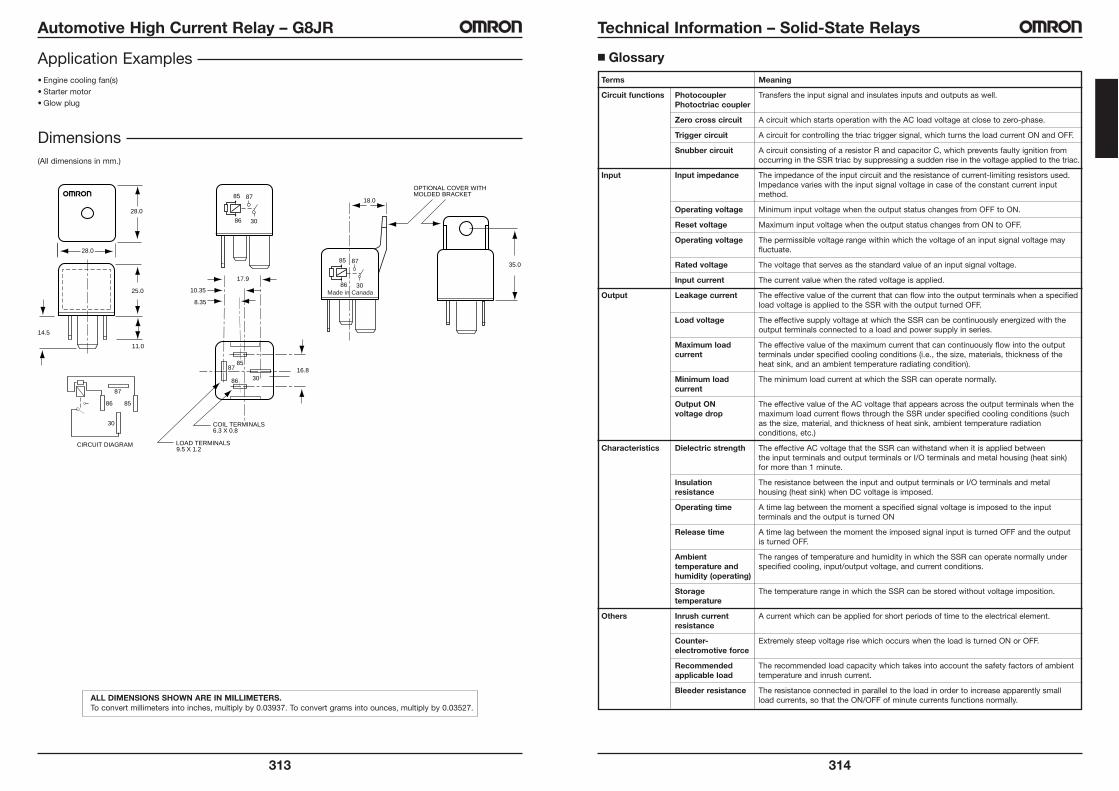
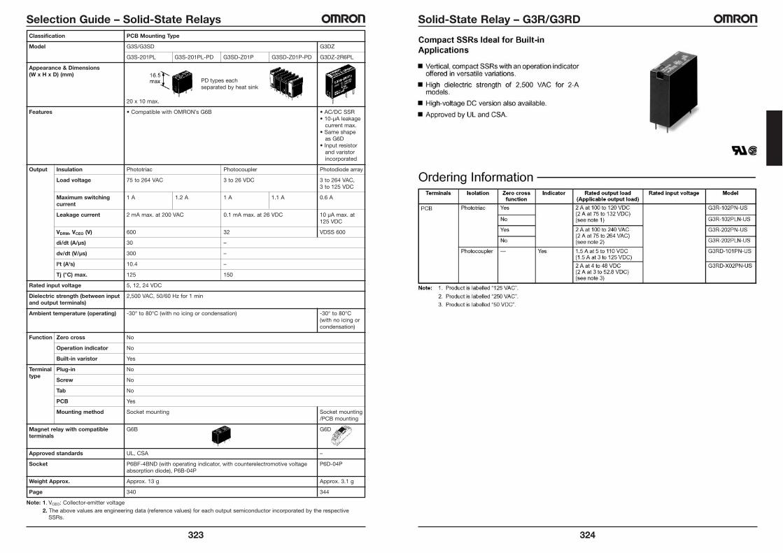
Automotive High Current Relay – G8JR
Application Examples• Engine cooling fan(s)• Starter motor• Glow plug
Dimensions(All dimensions in mm.)
ALL DIMENSIONS SHOWN ARE IN MILLIMETERS.To convert millimeters into inches, multiply by 0.03937. To convert grams into ounces, multiply by 0.03527.
316
Technical Information – Solid-State Relays
INPUT CONDITIONS
1. Input Voltage RipplesWhen there is a ripple in the input voltage, set so that the peakvoltage is lower than the maximum operating voltage and the rootvoltage is above the minimum operating voltage.
OPERATION AND STORAGE ENVIRONMENT PRECAUTIONS
Operation and Storage LocationsDo not operate or store the Relay in locations subject to directsunlight or ultraviolet rays. Otherwise the resin to deteriorate,thereby causing cracks and other damage to the case. Do notoperate or store the Relay in locations subject to exposure towater or chemicals. Otherwise rust, corrosion, and deteriorationof the resin will occur.Extended Storage of the SSRIf the SSR is stored for an extended period of time, the terminalwill be exposed to the air, reducing its solderability due to sucheffects as oxidation. Therefore, when installing a Relay onto aboard after a long time in storage, check the state of the solderbefore use. Also, take preventive measures so that the terminalswill not be exposed to water, oil, or solvents while they are stored. Vibration and ShockDo not subject the SSR to excessive vibration or shock.Otherwise the SSR will malfunction and may cause damage to theinternal components. To prevent the SSR from abnormalvibration, do not install the Unit in locations or by means that willsubject it to the vibrations from other devices, such as motors.SolventsDo not allow the SSR to come in contact with solvents such asthinners or gasoline. Doing so will dissolve the markings on theSSR.OilDo not allow the SSR terminal cover to come in contact with oil.Doing so will cause the cover to crack and become cloudy.PCB SSR Soldering1. SSRs must be soldered at 260°C within five seconds. For
models, however, that conform to separate conditions, performsoldering according to the specified requirements.
2. Use a rosin-based non-corrosive flux that is compatible withthe material of the SSR.
Ultrasonic CleaningDo not perform ultrasonic cleaning. Performing ultrasoniccleaning after the SSR base has been installed will causeultrasonic waves to resonate throughout the SSR internalstructure, thereby damaging the internal components.
FAIL-SAFE CONCEPT
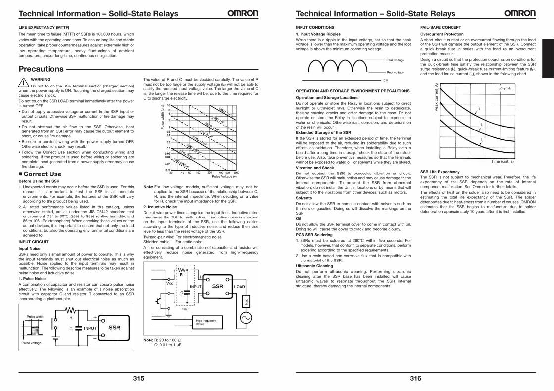
Overcurrent ProtectionA short-circuit current or an overcurrent flowing through the loadof the SSR will damage the output element of the SSR. Connecta quick-break fuse in series with the load as an overcurrentprotection measure.Design a circuit so that the protection coordination conditions forthe quick-break fuse satisfy the relationship between the SSRsurge resistance (IS), quick-break fuse current-limiting feature (IF),and the load inrush current (IL), shown in the following chart.
SSR Life ExpectancyThe SSR is not subject to mechanical wear. Therefore, the lifeexpectancy of the SSR depends on the rate of internalcomponent malfunction. See Omron for further details.The effects of heat on the solder also need to be considered inestimating the total life expectancy of the SSR. The solderdeteriorates due to heat-stress from a number of causes. OMRONestimates that the SSR begins to malfunction due to solderdeterioration approximately 10 years after it is first installed.
Time (unit: s)
IF
IL
IS
IS>IF >IL
Pea
k cu
rren
t (A
)
315
Technical Information – Solid-State Relays
LIFE EXPECTANCY (MTTF)
The mean time to failure (MTTF) of SSRs is 100,000 hours, whichvaries with the operating conditions. To ensure long life and stableoperation, take proper countermeasures against extremely high orlow operating temperature, heavy fluctuations of ambienttemperature, and/or long-time, continuous energization.
WARNING
Do not touch the SSR terminal section (charged section)when the power supply is ON. Touching the charged section maycause electric shock.Do not touch the SSR LOAD terminal immediately after the poweris turned OFF.• Do not apply excessive voltage or current to the SSR input or
output circuits. Otherwise SSR malfunction or fire damage mayresult.
• Do not obstruct the air flow to the SSR. Otherwise, heatgenerated from an SSR error may cause the output element toshort, or cause fire damage.
• Be sure to conduct wiring with the power supply turned OFF.Otherwise electric shock may result.
• Follow the Correct Use section when conducting wiring andsoldering. If the product is used before wiring or soldering arecomplete, heat generated from a power supply error may causefire damage.
Correct UseBefore Using the SSR1. Unexpected events may occur before the SSR is used. For this
reason it is important to test the SSR in all possibleenvironments. For example, the features of the SSR will varyaccording to the product being used.
2. All rated performance values listed in this catalog, unlessotherwise stated, are all under the JIS C5442 standard testenvironment (15° to 30°C, 25% to 85% relative humidity, and86 to 106 kPa atmosphere). When checking these values on theactual devices, it is important to ensure that not only the loadconditions, but also the operating environmental conditions areadhered to.
INPUT CIRCUIT
Input NoiseSSRs need only a small amount of power to operate. This is whythe input terminals must shut out electrical noise as much aspossible. Noise applied to the input terminals may result inmalfunction. The following describe measures to be taken againstpulse noise and inductive noise.1. Pulse NoiseA combination of capacitor and resistor can absorb pulse noiseeffectively. The following is an example of a noise absorptioncircuit with capacitor C and resistor R connected to an SSRincorporating a photocoupler.
The value of R and C must be decided carefully. The value of Rmust not be too large or the supply voltage (E) will not be able tosatisfy the required input voltage value. The larger the value of Cis, the longer the release time will be, due to the time required forC to discharge electricity.
Note: For low-voltage models, sufficient voltage may not beapplied to the SSR because of the relationship between C,R, and the internal impedance. When deciding on a valuefor R, check the input impedance for the SSR.
2. Inductive NoiseDo not wire power lines alongside the input lines. Inductive noisemay cause the SSR to malfunction. If inductive noise is imposedon the input terminals of the SSR, use the following cablesaccording to the type of inductive noise, and reduce the noiselevel to less than the reset voltage of the SSR.Twisted-pair wire: For electromagnetic noiseShielded cable: For static noiseA filter consisting of a combination of capacitor and resistor willeffectively reduce noise generated from high-frequencyequipment.
Note: R: 20 to 100 ΩC: 0.01 to 1 µF
Precautions
Pul
se w
idth
(µs)
Pulse Voltage (v)
318
Technical Information – Solid-State Relays
Mounting SSR to PCBRead the precautions for each model and fully familiarize yourselfwith the following when mounting the SSR to the PCB.
1. Do not bend the terminals to make theSSR self-standing, otherwise the fullperformance of the SSR may not bepossible.
2. Process the PCB properly in accordancewith the mounting dimensions.
1. The flux applied must be non-corrosive rosinflux, which is suitable to the materialof theSSR. Apply alcohol solvent to dissolve theflux.
2. Make sure that all parts of the SSR otherthan the terminals are free of the flux. Theinsulation resistance of the SSR may bedegraded if the flux is on the bottom of theSSR.
1. Be sure to preheat the SSR to allow bettersoldering.
2. Preheat the SSR under the followingconditions.
3. Do not use the SSR if it is left at hightemperature over a long time. This maychange the characteristics of the SSR.
Automatic Soldering1. Reflow soldering is recommended for
maintaining a uniform soldering quality.• Solder: JIS Z3282 or H63A• Soldering lead temperature:
Approx. 210°C max 10 secs• Soldering time: Approx. 5 s max. (Approx.
2 s for first time and approx. 3 s for secondtime for DWS)
• Perform solder level adjustments so thatthe solder will not overflow on the PCB.
Manual Soldering – see recommendedTemperature Profile1. After smoothing the tip of the soldering iron,
solder the SSR under the followingconditions.• Solder: JIS Z3282, 1160A, or H63A with
rosin-flux-cored solder• Soldering iron: 30 to 60 W• Soldering temperature: 260°C max.• Soldering time: Approx. 5 s max.
1. After soldering the SSR, be sure to cooldown the SSR so that the soldering heat willnot deteriorate the SSR or any othercomponent.
2. Do not dip the SSR into cold liquid, such asa detergent, immediately after soldering theSSR.
1. Refer to the following table for the selectionof the cleaning method and detergent.
Detergent
Boiling cleaning or dip cleaning is availableto the SSR. Do not cut the terminals,otherwise the internal parts of the SSR maybe damaged. Make sure that thetemperature of the detergent is within thepermissible ambient operating temperatureof the SSR.
2. Availability of Detergents
Note: 1. Contact your OMRON representativesbefore using any other detergent. Donot apply Freon TMC, paint thinner, orgasoline to any SSR.2. The space between the SSR andPCB may be not be adequatelycleaned with a hydrocarbon or alcoholdetergent.
Actions are being taken worldwide to stopthe use of CFC-113 (chlorofluorocarbon) and1.1.1 trichloroethane. Your understandingand cooperation are highly appreciated.
1. Do not fix the whole SSR with resin,otherwise the characteristics of the SSRmay change.
2. The temperature of the coating materialmust be within the permissible ambientoperating temperature range.
Detergent Availability
Chlorine Perochine OKdetergent Chlorosolder
Trichloroethylene
Aqueous Indusco OKdetergent Holys
Pure water(pure hot water)
Alcohol IPA OKEthanol
Others Paint thinner NGGasoline
Detergent Availability
Epoxy OK
Urethane OK
Silicone OK
Temperature 150° C max.
Time 60-90 secs.
317
Technical Information – Solid-State Relays
HANDLING THE SSR
Do Not DropThe SSR is a high-precision component. Do not drop the SSR or subject it to excessive vibration or shock regardless of whether the SSRis mounted or not.The maximum vibration and shock that an SSR can withstand varies with the model. Refer to the relevant datasheet.The SSR cannot maintain its full performance capability if the SSR is dropped or subjected to excessive vibration or shock resulting inpossible damage to its internal components.The impact of shock given to the SSR that is dropped varies upon the case, and depends on the floor material, the angle of collision withthe floor, and the dropping height. For example, if a single SSR is dropped on a plastic tile from a height of 10 cm, the SSR may receivea shock of 1,000 m/s2 or more.Handle the SSR models in in-line packages with the same care and keep them free from excessive vibration or shock.
PCB-MOUNTING SSR
Suitable PCB1. PCB Material
PCBs are classified into epoxy PCBs and phenol PCBs. The following table lists the characteristics of these PCBs. Select onetaking into account the application and cost. Epoxy PCBs are recommended for SSR mounting in order to prevent the solder fromcracking.
2. PCB ThicknessThe PCB may warp due to the size, mounting method, or ambientoperating temperature of the PCB or the weight of parts mountedto the PCB. Should warping occur, the internal mechanism of theSSR on the PCB will be deformed and the SSR may not provideits full capability. Determine the thickness of the PCB by takingthe material of the PCB into consideration.3. Terminal Hole and Land DiametersRefer to the following table to select the terminal hole and landdiameters based on the SSR mounting dimensions. The landdiameter may be smaller if the land is processed with through-hole plating.
MOUNTING SPACE
The ambient temperature around the sections where the SSR ismounted must be within the permissible ambient operatingtemperature. If two or more SSRs are mounted closely together,the SSRs may radiate excessive heat. Therefore, make sure thatthe SSRs are separated from one another at the specifieddistance provided in the datasheet. If there is no such provision,maintain a space that is as wide as a single SSR. Provide adequate ventilation to the SSRs as shown in thefollowing
Hole Dia. (mm) Minimum land dia. (mm)
Nominal Tolerancevalue
0.6 ±0.1 1.5
0.8 1.8
1.0 2.0
1.2 2.5
1.3 2.5
1.5 3.0
1.6 3.0
2.0 3.0
Item Epoxy Phenol
Glass epoxy Paper epoxy Paper phenol
Electricalcharacteristics
Mechanicalcharacteristics
Economical Expensive Rather expensive Inexpensiveefficiency
Application
High insulation resistance.Highly resistive to moistureabsorption.
The dimensions are not easilyaffected by temperature or humidity.Ideal for through-hole or multi-layerPCBs.
Applications that require highreliability.
Applications that may require lessreliability than those for glass epoxyPCBs but require more reliabilitythan those of paper phenol PCBs.
Applications in comparativelygood environments withlong-density wiring.
Inferior to glass epoxy butsuperior to paper phenol PCBs.
The dimensions are easily affectedby temperature or humidity.Not suitable for through-holePCBs.
Inferior to glass epoxy butsuperior to paper phenol PCBs.
New PCBs are highly insulation-resistive but easily affected bymoisture absorption and cannotmaintain good insulationperformance over a long time.
320
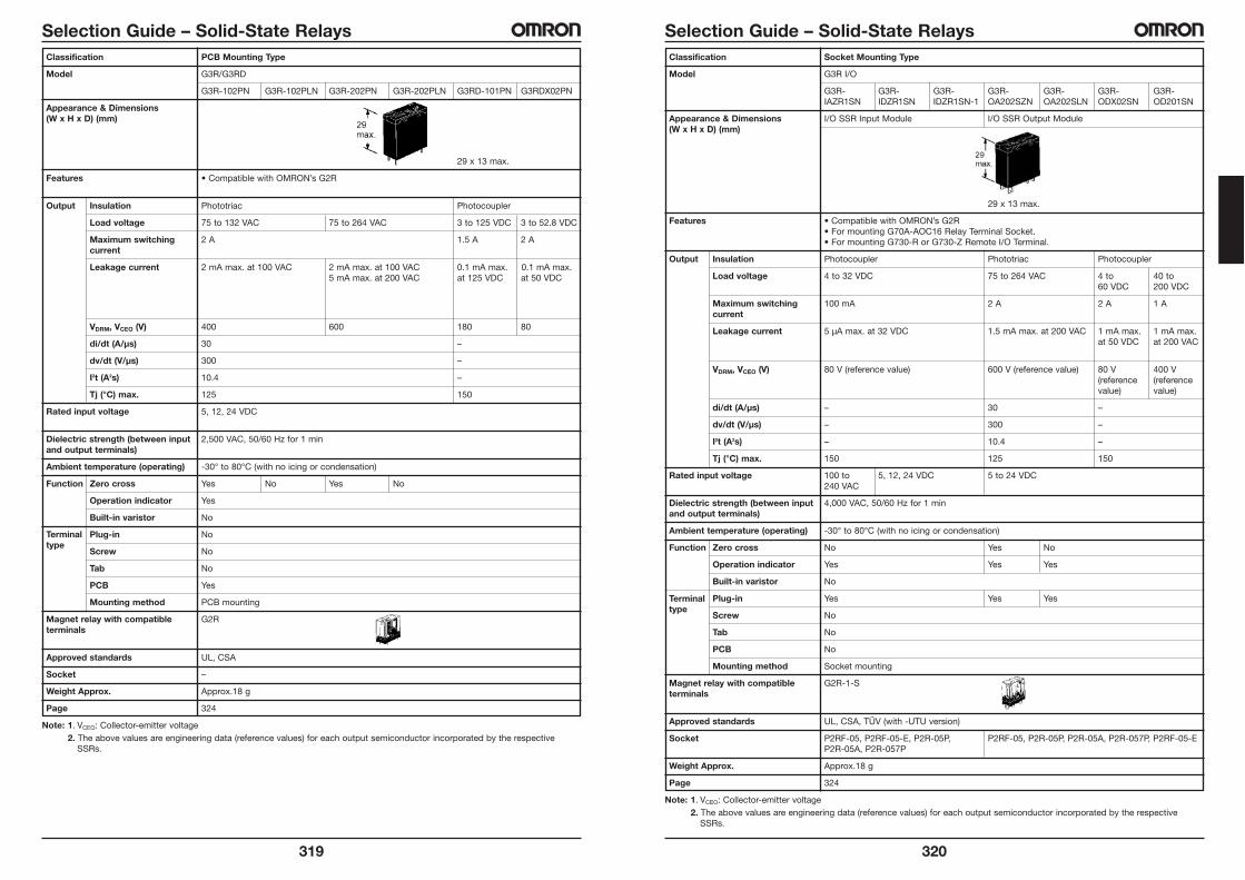
Selection Guide – Solid-State RelaysClassification Socket Mounting Type
Model G3R I/O
G3R- G3R- G3R- G3R- G3R- G3R- G3R-IAZR1SN IDZR1SN IDZR1SN-1 OA202SZN OA202SLN ODX02SN OD201SN
Appearance & Dimensions I/O SSR Input Module I/O SSR Output Module(W x H x D) (mm)
29 x 13 max.
Features • Compatible with OMRON’s G2R• For mounting G70A-AOC16 Relay Terminal Socket.• For mounting G730-R or G730-Z Remote I/O Terminal.
Output Insulation Photocoupler Phototriac Photocoupler
Load voltage 4 to 32 VDC 75 to 264 VAC 4 to 40 to60 VDC 200 VDC
Maximum switching 100 mA 2 A 2 A 1 Acurrent
Leakage current 5 µA max. at 32 VDC 1.5 mA max. at 200 VAC 1 mA max. 1 mA max.at 50 VDC at 200 VAC
VDRM, VCEO (V) 80 V (reference value) 600 V (reference value) 80 V 400 V(reference (referencevalue) value)
di/dt (A/µs) – 30 –
dv/dt (V/µs) – 300 –
I2t (A2s) – 10.4 –
Tj (°C) max. 150 125 150
Rated input voltage 100 to 5, 12, 24 VDC 5 to 24 VDC240 VAC
Dielectric strength (between input 4,000 VAC, 50/60 Hz for 1 minand output terminals)
Ambient temperature (operating) -30° to 80°C (with no icing or condensation)
Function Zero cross No Yes No
Operation indicator Yes Yes Yes
Built-in varistor No
Plug-in Yes Yes Yes
Screw No
Tab No
PCB No
Mounting method Socket mounting
Magnet relay with compatible G2R-1-Sterminals
Approved standards UL, CSA, TÜV (with -UTU version)
Socket P2RF-05, P2RF-05-E, P2R-05P, P2RF-05, P2R-05P, P2R-05A, P2R-057P, P2RF-05-EP2R-05A, P2R-057P
Weight Approx. Approx.18 g
Page 324
Note: 1. VCEO: Collector-emitter voltage2. The above values are engineering data (reference values) for each output semiconductor incorporated by the respective
SSRs.
Terminaltype
319
Selection Guide – Solid-State RelaysClassification PCB Mounting Type
Model G3R/G3RD
G3R-102PN G3R-102PLN G3R-202PN G3R-202PLN G3RD-101PN G3RDX02PN
Appearance & Dimensions(W x H x D) (mm)
29 x 13 max.
Features • Compatible with OMRON’s G2R
Output Insulation Phototriac Photocoupler
Load voltage 75 to 132 VAC 75 to 264 VAC 3 to 125 VDC 3 to 52.8 VDC
Maximum switching 2 A 1.5 A 2 Acurrent
Leakage current 2 mA max. at 100 VAC 2 mA max. at 100 VAC 0.1 mA max. 0.1 mA max.5 mA max. at 200 VAC at 125 VDC at 50 VDC
VDRM, VCEO (V) 400 600 180 80
di/dt (A/µs) 30 –
dv/dt (V/µs) 300 –
I2t (A2s) 10.4 –
Tj (°C) max. 125 150
Rated input voltage 5, 12, 24 VDC
Dielectric strength (between input 2,500 VAC, 50/60 Hz for 1 minand output terminals)
Ambient temperature (operating) -30° to 80°C (with no icing or condensation)
Function Zero cross Yes No Yes No
Operation indicator Yes
Built-in varistor No
Plug-in No
Screw No
Tab No
PCB Yes
Mounting method PCB mounting
Magnet relay with compatible G2Rterminals
Approved standards UL, CSA
Socket –
Weight Approx. Approx.18 g
Page 324
Note: 1. VCEO: Collector-emitter voltage2. The above values are engineering data (reference values) for each output semiconductor incorporated by the respective
SSRs.
Terminaltype
322
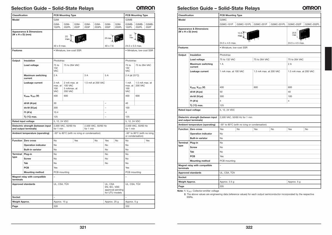
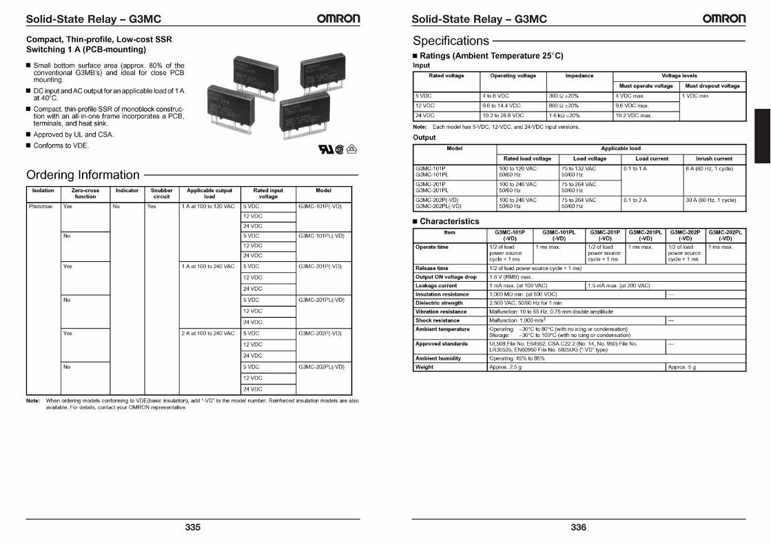
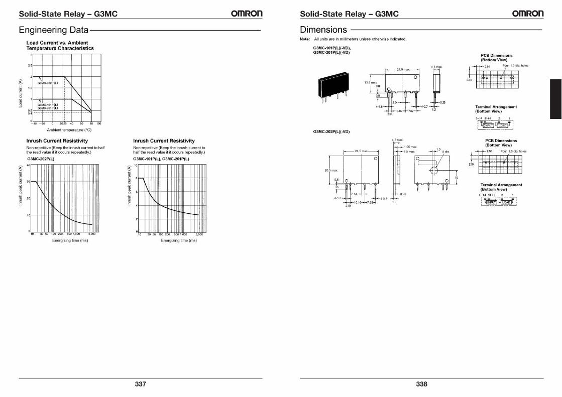
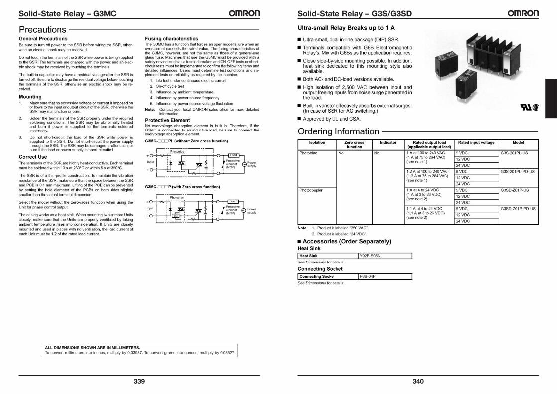
Selection Guide – Solid-State RelaysClassification PCB Mounting Type
Model G3MC
G3MC-101P G3MC-101PL G3MC-201P G3MC-201PL G3MC-202P G3MC-202PL
Appearance & Dimensions(W x H x D) (mm)
24.5 x 4.5 max. 24.5 x 4.5 max.
Features • Miniature, low-cost SSR
Output Insulation Phototriac
Load voltage 75 to 132 VAC 75 to 264 VAC 75 to 264 VAC
Maximum switching 1 A 2 Acurrent
Leakage current 1 mA max. at 100 VAC 1.5 mA max. at 200 VAC 1.5 mA max. at 200 VAC
VDRM, VCEO (V) 400 600 600
di/dt (A/µs) 50 40
dv/dt (V/µs) 300 100
I2t (A2s) 4 4
Tj (°C) max. 125
Rated input voltage 5, 12, 24 VDC
Dielectric strength (between input 2,500 VAC, 50/60 Hz for 1 minand output terminals)
Ambient temperature (operating) -30° to 80°C (with no icing or condensation)
Function Zero cross Yes No Yes No Yes No
Operation indicator No
Built-in varistor No
Plug-in No
Screw No
Tab No
PCB Yes
Mounting method PCB mounting
Magnet relay with compatible –terminals
Approved standards UL, CSA, TÜV
Socket –
Weight Approx. Approx. 2.5 g Approx. 5 g
Page 335
Note: 1. VCEO: Collector-emitter voltage2. The above values are engineering data (reference values) for each output semiconductor incorporated by the respective
SSRs.
Terminaltype
321
Selection Guide – Solid-State RelaysClassification PCB Mounting Type PCB Mounting Type
Model G3M G3MB
G3M- G3M- G3M- G3M- G3M- G3M- G3M- G3MB- G3MB- G3MB-102PL 202PL 202P 203P 203PL 205P 205PL 102PL 202PL 202P
Appearance & Dimensions(W x H x D) (mm)
40 x 9 max. 40 x 7.6 24.5 x 5.5 max.
Features • Miniature, low-cost SSR • Miniature, low-cost SSR
Output Insulation Phototriac Phototriac
Load voltage 75 to 75 to 264 VAC 75 to 75 to 264 VAC132 132VAC VAC
Maximum switching 2 A 3 A 5 A 2 A (at 25°C)current
Leakage current 2 mA 2 mA max. at 1.5 mA at 200 VAC 1 mA 1.5 mA max. atmax. at 100 VAC max. at 200 VAC100 5 mAmax. at 100VAC 200 VAC VAC
VDRM, VCEO (V) 400 600 400 600
di/dt (A/µs) 30 – 40
dv/dt (V/µs) 300 – 100
I2t (A2s) 10.4 – 4
Tj (°C) max. 125 – 125
Rated input voltage 5, 12, 24 VDC 5, 12, 24 VDC
Dielectric strength (between input 2,000 VAC, 50/60 Hz 2,500 VAC, 50/60 Hz 2,500 VAC, 50/60 Hzand output terminals) for 1 min for 1 min for 1 min
Ambient temperature (operating) -30° to 80°C (with no icing or condensation) -30° to 80°C (with no icingor condensation)
Function Zero cross No Yes No Yes No No Yes
Operation indicator No No No
Built-in varistor No No No
Plug-in No No No
Screw No No No
Tab No No No
PCB Yes Yes
Mounting method PCB mounting PCB mounting
Magnet relay with compatible – –terminals
Approved standards UL, CSA, TÜV UL, CSA UL, CSA, TÜVEN, IEC, VDE:approval pendingfor UTU models
Socket – –
Weight Approx. Approx. 15 g Approx. 25 g Approx. 5 g
Page 328 332
Terminaltype
324
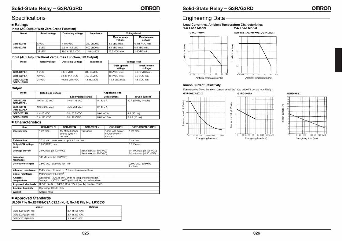
Solid-State Relay – G3R/G3RD
323
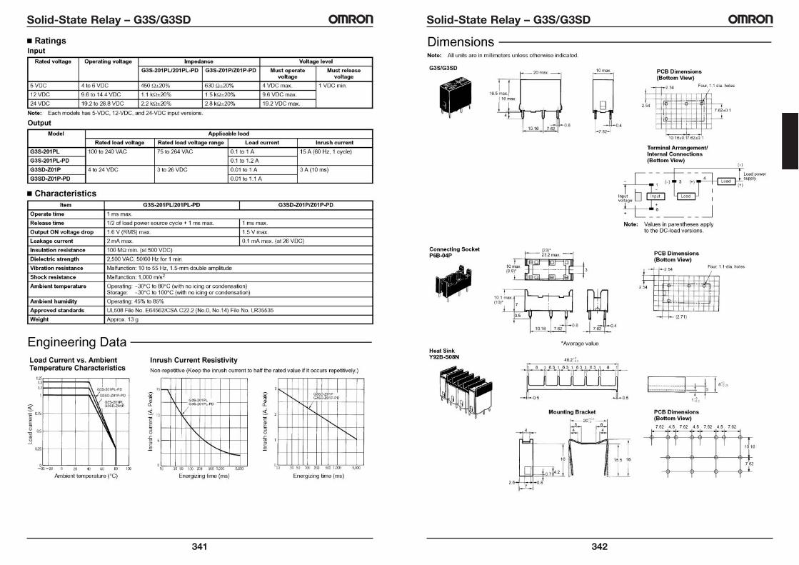
Selection Guide – Solid-State RelaysClassification PCB Mounting Type
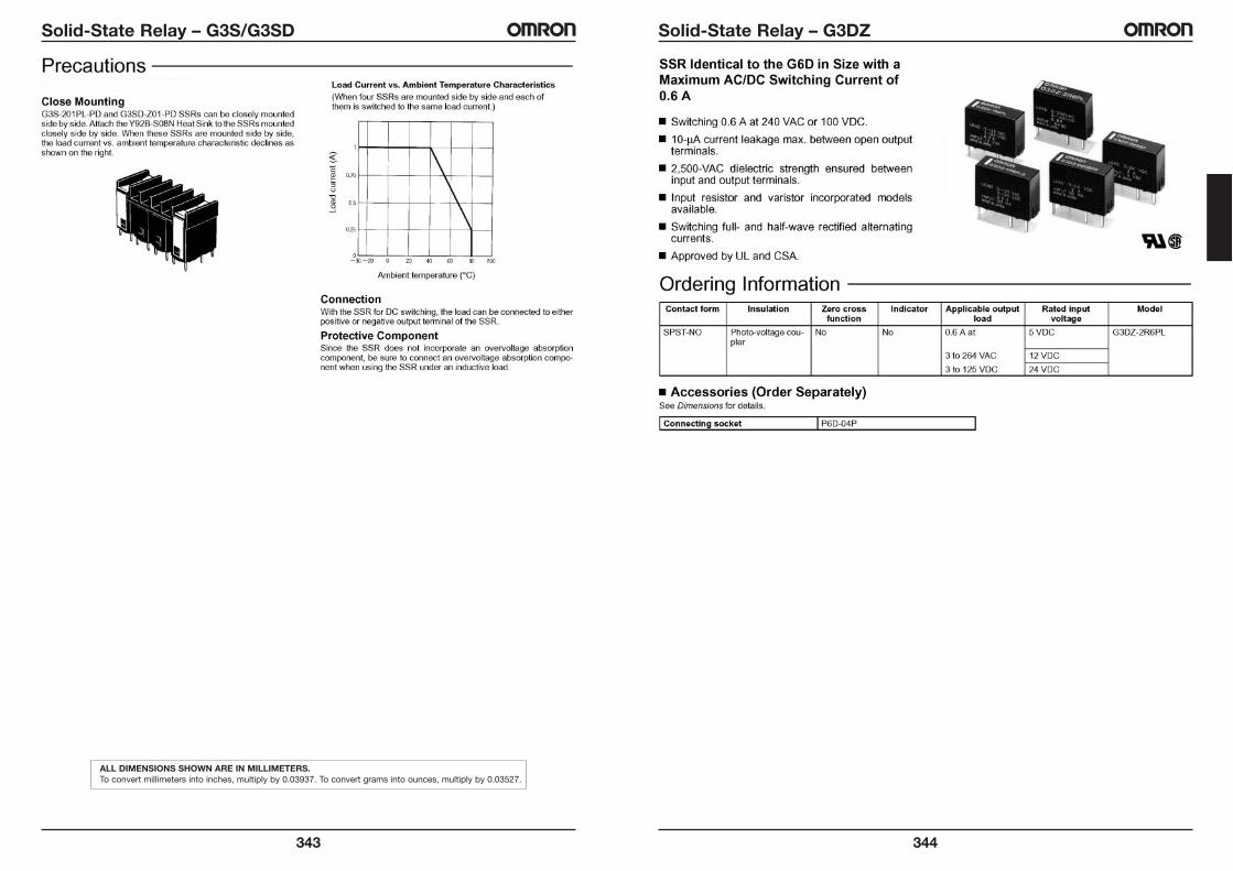
Model G3S/G3SD G3DZ
G3S-201PL G3S-201PL-PD G3SD-Z01P G3SD-Z01P-PD G3DZ-2R6PL
Appearance & Dimensions(W x H x D) (mm)
20 x 10 max.
Features • Compatible with OMRON’s G6B • AC/DC SSR• 10-µA leakage
current max.• Same shape
as G6D• Input resistor
and varistorincorporated
Output Insulation Phototriac Photocoupler Photodiode array
Load voltage 75 to 264 VAC 3 to 26 VDC 3 to 264 VAC,3 to 125 VDC
Maximum switching 1 A 1.2 A 1 A 1.1 A 0.6 Acurrent
Leakage current 2 mA max. at 200 VAC 0.1 mA max. at 26 VDC 10 µA max. at125 VDC
VDRM, VCEO (V) 600 32 VDSS 600
di/dt (A/µs) 30 –
dv/dt (V/µs) 300 –
I2t (A2s) 10.4 –
Tj (°C) max. 125 150
Rated input voltage 5, 12, 24 VDC
Dielectric strength (between input 2,500 VAC, 50/60 Hz for 1 minand output terminals)
Ambient temperature (operating) -30° to 80°C (with no icing or condensation) -30° to 80°C (with no icing orcondensation)
Function Zero cross No
Operation indicator No
Built-in varistor Yes
Plug-in No
Screw No
Tab No
PCB Yes
Mounting method Socket mounting Socket mounting/PCB mounting
Magnet relay with compatible G6B G6Dterminals
Approved standards UL, CSA –
Socket P6BF-4BND (with operating indicator, with counterelectromotive voltage P6D-04Pabsorption diode), P6B-04P
Weight Approx. Approx. 13 g Approx. 3.1 g
Page 340 344
Note: 1. VCEO: Collector-emitter voltage2. The above values are engineering data (reference values) for each output semiconductor incorporated by the respective
SSRs.
Terminaltype
PD types eachseparated by heat sink
326
Solid-State Relay – G3R/G3RD
325
Solid-State Relay – G3R/G3RD
328
Solid-State Relay – G3M
Zero Cross Models Added toCompact, Low-cost G3M Series This design for high-density PCB applications.
DC input-AC output for up to 5-A load.
Approved by UL and CSA.
327
Solid-State Relay – G3R/G3RD
ALL DIMENSIONS SHOWN ARE IN MILLIMETERS.To convert millimeters into inches, multiply by 0.03937. To convert grams into ounces, multiply by 0.03527.
330
Solid-State Relay – G3M
329
Solid-State Relay – G3M
332
Solid-State Relay – G3MB
331
Solid-State Relay – G3M
ALL DIMENSIONS SHOWN ARE IN MILLIMETERS.To convert millimeters into inches, multiply by 0.03937. To convert grams into ounces, multiply by 0.03527.
334
Solid-State Relay – G3MB
ALL DIMENSIONS SHOWN ARE IN MILLIMETERS.To convert millimeters into inches, multiply by 0.03937. To convert grams into ounces, multiply by 0.03527.
333
Solid-State Relay – G3MB
336
Solid-State Relay – G3MC
335
Solid-State Relay – G3MC
338
Solid-State Relay – G3MC
337
Solid-State Relay – G3MC
340
Solid-State Relay – G3S/G3SD
339
Solid-State Relay – G3MC
ALL DIMENSIONS SHOWN ARE IN MILLIMETERS.To convert millimeters into inches, multiply by 0.03937. To convert grams into ounces, multiply by 0.03527.
342
Solid-State Relay – G3S/G3SD
341
Solid-State Relay – G3S/G3SD
344
Solid-State Relay – G3DZ
343
Solid-State Relay – G3S/G3SD
ALL DIMENSIONS SHOWN ARE IN MILLIMETERS.To convert millimeters into inches, multiply by 0.03937. To convert grams into ounces, multiply by 0.03527.
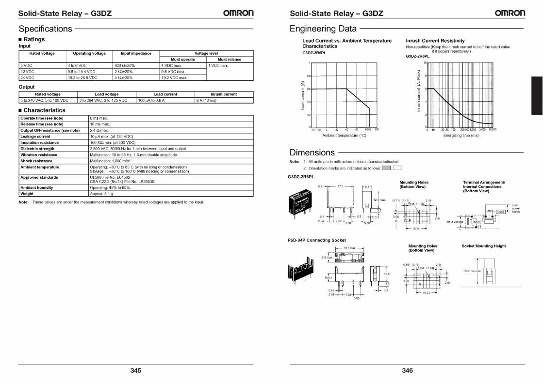
346
Solid-State Relay – G3DZ
345
Solid-State Relay – G3DZ
348
Technical Information – MOSFET Relays
IntroductionNew models and a wider range provide an array of solutions,meeting the needs of today’s high performance applications.Our new range of MOSFET relays, Type G3VM, set the benchmarkin Solid State Relays (SSRs). Products are manufactured usingthe latest advances in automated production and include a varietyof improved construction technologies within the areas of theinput LED, PDA (Photo Diode Array used as a photocoupler) andMOSFET chips used in the load switching circuit. As a result,further reductions in package size and power requirements havebeen achieved.Combining the advantages of mechanical and solid statetechnology, the new G3VM range gives you unprecedentedcapability to design. All models featured include a doubleMOSFET load circuit, enabling the designer complete versatilitysince it makes no difference whether an AC or DC load in eitherdirection is connected (Connection A). Thus, the MOSFET relay isa fully functional alternative to an electromechanical relay withminimal additional drive circuitry.
The built-in Current Limit Function (CLR models) has many uses.Traditionally used to clamp excessive over current fault conditionsin telecom equipment, this feature can also be used to good effectto resist transient and short circuit conditions.MOSFET relays are the ideal data and telecommunication solutionfor line seizing, line switching, hook switching, Data AccessArrangement (DAA) function, line transformer circuit control andother feature phone functions. Central office applications requirehigh reliability and long life. Here G3VM is ideal for use in theareas of Subscriber Line Interfaces (SLICs) Multiplexers andRouters. In addition, Local Area Networks (LANs) and NetworkTermination Units (NTUs) including Set-Top Boxes (STBs) andRemote Metering Systems (RMS) can take advantage of theG3VMs’ small size and low ON resistance.Advances in performance and cost reduction enable MOSFETrelays to be considered as good alternatives to Reed Relays inapplication areas such as security motion detectors (standard andanti-mask PIRs), other surveillance alarm equipment andassociated systems.
Glossary
Term Symbol Description
Rated current that can flow continuously in the forward direction of the LED
Rated current that can flow momentarily in the forward direction of the LED
Rated change of forward current flowing through the LED relative to ambienttemperature above 25 °C
Rated reverse voltage that can be applied between the anode and the cathode
Rated temperature that can be allowed in the junction of the LED, Photodetectoror MOSFET(s)
Rated voltage that can be applied between the MOSFET's output terminalsin the OFF state
Rated current that can flow between the MOSFET's output terminals in the ON state
Rated change of load current flowing between MOSFET(s) output terminals relativeto ambient temperature above 25 °C
Isolation voltage between input and output terminals for a specified time
Ambient temperature range in which the relay may be operated without impairment
Ambient temperature range in which the relay may be stored while not operating
Voltage drop between the LED's anode and cathode at a certain forward current
Leakage current flowing in the LED's reverse direction (between cathode and anode)
Electrostatic capacitance between the anode and the cathode terminals of the LED
Minimum value of input current necessary to put the output MOSFET(s)in to the ON state
Resistance between the MOSFET's output terminals specified with reference to ONstate current
Leakage current flowing between the MOSFET's output terminals in the OFF state
Electrostatic capacitance between the input and output terminals of the relay
Resistance between the input and output terminals at the specified voltage value
Time required for the output waveform to change from 0(100%) to 90(10%) after inputgoes from OFF to ON state
Time required for the output waveform to change from 0(100%) to 90(10%) after inputgoes from ON to OFF state
Rated load voltage that can be applied between the MOSFET's output terminals
LED forward current
Repetitive peak LED forwardcurrent
LED forward current reductionrate
LED reverse voltage
Connection temperature
Output dielectric strength
Continuous load current
ON current reduction rate
Dielectric strength betweeninput and output
Operating temperature
Storage temperature
LED forward voltage
LED reverse current
Capacity between LED terminals
Trigger LED forward current
Maximum resistance with outputON
Current leakage when the relayis open
Capacity between I/O terminals
Insulation resistance
Turn-ON time
Turn-OFF time
Output dielectric strength
IF
IFP
<ION/°C
VR
TJ
VOFF
IO
<ION/°C
VI-O
Ta
Tstg
VF
IR
CT
IFT
RON
ILEAK
CI-O
RI-O
tON
tOFF
VDD
347
Solid-State Relay – G3DZ
ALL DIMENSIONS SHOWN ARE IN MILLIMETERS.To convert millimeters into inches, multiply by 0.03937. To convert grams into ounces, multiply by 0.03527.