Embed Size (px)
Citation preview

Peter Kinget
(In collaboration with S. Chatterjee and Y. Tsividis)
0.5V AnalogIntegrated Circuits
Department of Electrical Engineering
www.cisl.columbia.edu
Analog, Digital, Mixed-Mode and RF Integrated Circuits

© Kinget 2005 3
Analog, Mixed Signal and RF Integrated Circuit Design Research
Ultra-low voltage circuits: 0.5V
RF integratedoscillators
Ultra-widebandRF circuits
Injection lockedcircuits
Biological Interfaces
Device mismatch & its influence onAnalog & RF ics

© Kinget 2005 4
Sample of Recent Chips

© Kinget 2005 5
Outline
• Why 0.5 V Analog Integrated Circuits?
• Design Challenges & Opportunities at 0.5 V.
• 0.5 V Operational Transconductance Amplifiers.
• 0.5 V Biasing circuits.
• 0.5 V Fully Integrated Active RC filter with on-chip automatic tuning.
• Conclusions.

© Kinget 2005 6
Analog in a Mixed Signal World• Sounds, images, EM waves, …. are ANALOG.• Information processing & storage are DIGITAL.• System-on-chip is powerful economic paradigm.
• Digital drives technology development & choice.
If Analog can be done in a digital technology, it will be done.
Most Digital ICs need some Analog!
D & A A & D A & D

© Kinget 2005 7
CMOS Trends: Supply Voltage
Analog VDD
Digital VDD
Digital VT
Technology node [nm]
[ITRS'04]
–O– High Perf.–∆– Low Standby–V– Low Power

© Kinget 2005 8
CMOS Trends: On chip Clock Speed
[ITRS'04]
Technology node [nm]

© Kinget 2005 9
MOS transistor
• Transconductor or Current SourceVDS > 0.15V (for VGS-VT ≤ 0.2)
• Switch/Resistoronly for very small signal range !?
SwitchResistor:
TransconductorWeak
Inversion
StrongInversion
0.24µm/0.36µm nMOSin 0.18µm CMOS
5φT

© Kinget 2005 10
Common Source Amplifier
0.15 V
0.15 V
0.2 Vpp
0.5 + 0.15 V
0.5 V
VT= 0.5 V VDS,sat= 0.15 V

© Kinget 2005 11
Common Drain Buffer
0.15 V
0.15 V
0.2 Vpp
0.5 + 0.15 + 0.1 + 0.15 V
0.5 V
VT= 0.5 V VDS,sat= 0.15 V

© Kinget 2005 12
Common Gate Amplifier / Cascode
0.15 V
0.15 V0.5 + 0.15 + x + 0.15 V
0.5 V
VT= 0.5 V VDS,sat= 0.15 V
0.15 V

© Kinget 2005 13
Differential OTA design challenges
0.15 V
0.5 V
0.65 V
0.8 V
-0.15 V
0.15 V
0.15 V
0.3 - 0.35 V
0.5 V
0.1 V
0.4 V0.4 V
0.1 V0.15 - 0.35 V
0.4 V
0.25 V
VT= 0.5 V VDS,sat= 0.15 V

© Kinget 2005 14
CMFB in Folded Cascode OTA
Common Mode Feedback requires ‘fast’ amplifier operating from Vout,CM= VDD/2 !?

© Kinget 2005 15
Challenges at 0.5 V• VDS,sat related challenges:
– Independent of region of operation!– Independent of VT!– Signal swings are limited.– Avoid transistor stacks.
• VGS related challenges:– Depend on region of operation & (VGS-VT).– Depend on VT!– Avoid signal swing on gate.

© Kinget/Chatterjee/Tsividis 16
‘Feedback to the rescue’
CM @ OTA-in > CM @ input and output
[Kar00] [Bul00]
© Kinget/Chatterjee/Tsividis 17
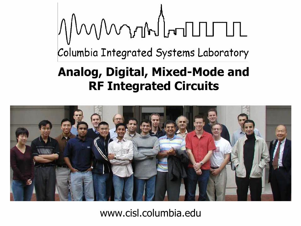
Opportunities at 0.5 V: MOS 4-terminal device
Body
Source
Drain
Gate
G D BS Sub
n+
n+n+n+ n+p+ p+
p
p
nMOS cross section(deep n-well process)
nMOS circuit equivalent(deep n-well process)

© Kinget/Chatterjee/Tsividis 18
Opportunities at 0.5 V• Body terminal
– Signal input: [Guz87]– VTH reduction & control
[Kob94], [Von94]– Bias control
• Latch-up not an issue– Assuming VDD and GND are
‘well behaved’.• Techniques can be ported
to ‘double gate’ devices
VBS 0.5 V
500
0
VTH
mV
300
430360
0.0
VGS 0.5 V0.2
3
0
IDS VBS ↑
µA
0.24µm/0.36µm nMOSin 0.18µm CMOS

0.5 V Body-input OTA

© Kinget/Chatterjee/Tsividis 20
Low-voltage differential-gain stage
0.15 - 0.35 V
0.5 V0.25 V
0.25 V
0.25 V
0.07 V

© Kinget/Chatterjee/Tsividis 21
Single-stage gain, CMRR
Differential mode load: gds
Common mode load: (gm1 + gm3)

© Kinget/Chatterjee/Tsividis 22
Two-stage fully-differential OTA
Pole splitting using Miller capacitor

© Kinget/Chatterjee/Tsividis 23
Setup for open-loop measurements
0.18 µm CMOS

© Kinget/Chatterjee/Tsividis 24
Open loop frequency response
DC gain: 52 dBGBW: 2.5 MHz
Phase Margin: 450
Frequency [Hz]
Simulation
Measurement

© Kinget/Chatterjee/Tsividis 25
Bulk-input OTA performanceC
lose
d lo
opO
pen
loop

0.5 V Gate-input OTA

© Kinget/Chatterjee/Tsividis 27
Setting common-mode voltages
0.5 V
0.4 V
0.4 V
0.5 V
Rb = 2/3 • Ri||Rf
0.25 V 0.25 V

© Kinget/Chatterjee/Tsividis 28
0.5 V OTA gate-input stage
© Kinget/Chatterjee/Tsividis 29
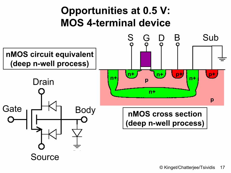
Two stage OTA
• Common-mode output of first stage is 0.4 V
0.25 V
0.4 V
0.4 V

© Kinget/Chatterjee/Tsividis 30
Two-stage fully differential 0.5 V OTA with Miller compensation

© Kinget/Chatterjee/Tsividis 31
Open Loop Performance (meas.)
Frequency [Hz]
Gai
n [d
B]
42 dB
GBW: 10 MHz
CL= 10pF (diff.)RL= 50kΩIDD= 150 µA
62 dB 350mV; automatic bias

© Kinget/Chatterjee/Tsividis 32
66.711.413289.5100 η [1/V]
----Depl.MOS
Lat.BJT
-Lat.BJT
SpecialDevices
0.180.180.50.72.50.50.352Techn. [um]
DDDSSSSSSE/Diff.101014-1220722CL [pF]75110-4600.5-5300Power [uW]102.541.36e-31.30.21.3GBW [MHz]
50/6252598470537049ADC [dB]0.50.50.91.30.90.811VDD [V]
G-IB-I[Pel98]
[Fer96]
[Sto02]
[Leh01]
[Las00]
[Bla98]

On-chip automatic biasing circuits

© Kinget/Chatterjee/Tsividis 34
On-chip biasing circuits
Vbn generating circuit
Level shift biasing circuit
(Simplified OTA)

© Kinget/Chatterjee/Tsividis 35
Error amplifier for biasing
• 20 kHz GBW for 1 pF load• 2 µA current• Controlled body voltage sets the amplifier threshold
Vin Vout
Vou
t[V
]
Vin [V]

© Kinget/Chatterjee/Tsividis 36
OTA dc transfer characteristics and VNR generation
VNR generating circuit
Replica of OTA stage 1
Input differential voltage [mV]
Out
put d
i ff v
olta
g e [V
]
Increasing VNR

© Kinget/Chatterjee/Tsividis 37
Open Loop Performance (meas.)
Frequency [Hz]
Gai
n [d
B]
42 dB
GBW: 10 MHz
CL= 10pF (diff.)RL= 50kΩIDD= 150 µA
62 dB 350mV; automatic bias

0.5 V Continuous time tunable active RC Filter

© Kinget/Chatterjee/Tsividis 39
0.5 V 5th order elliptic LPF
Frequency [Hz]
Gai
n [d
B]
280 kHz
135 kHz
© Kinget/Chatterjee/Tsividis 40
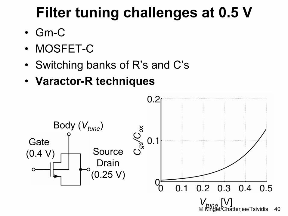
Filter tuning challenges at 0.5 V• Gm-C• MOSFET-C• Switching banks of R’s and C’s• Varactor-R techniques
Vtune [V]
Cgs
/Cox
Gate (0.4 V) Source
Drain (0.25 V)
Body (Vtune)

© Kinget/Chatterjee/Tsividis 41
Low-voltage tunable integrator
0.25 V 0.25 V
0.4 V
+
-Vin Vout
+
-
VDD
VDD

© Kinget/Chatterjee/Tsividis 42
Die photograph
• 0.18 µm CMOS
• MIM capacitors
• High-res resistors
• Standard VT
• Triple well devices
Filter PLL
Biasing circuits
OTAs
1mm
1mm

© Kinget/Chatterjee/Tsividis 43Frequency [Hz]
Gai
n [d
B]
Measured filter response for different supply voltages

© Kinget/Chatterjee/Tsividis 44
Measured filter response for different tuning voltages
Frequency [Hz]
Gai
n [d
B]
88 - 154 kHz(1.75x)
© Kinget/Chatterjee/Tsividis 45
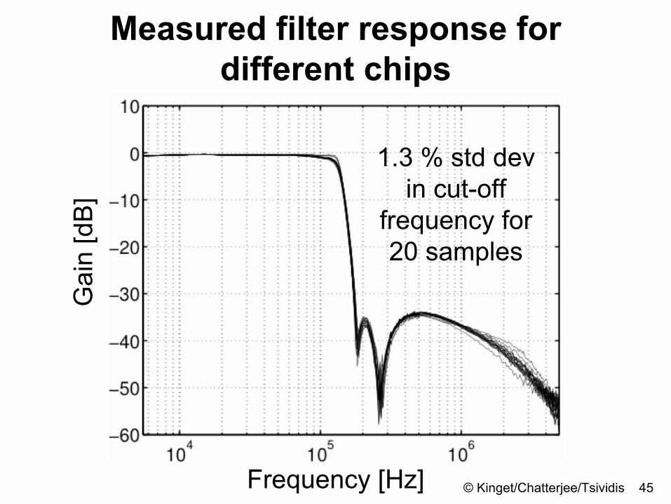
Measured filter response for different chips
Frequency [Hz]
Gai
n [d
B]
1.3 % std dev in cut-off
frequency for 20 samples

© Kinget/Chatterjee/Tsividis 46
Measured 3rd order inter-modulation
25 kHz
20 kHz
15 kHz
30 kHz
40 dB
Input differential rms amplitude [V]
Out
put d
iffe r
entia
l rm
s am
plitu
d e [ V
]

Effect of gain enhancement
Frequency [Hz]
Gai
n [d
B]
Without gain-enhancement
With gain-enhancement

© Kinget/Chatterjee/Tsividis 48
Performance summary at 27C
727285104VCO feed-thru @280kHz [µV rms]
69.0150.5
84.5148.0
88.0154.5
96.5153.0
Tuning range [kHz] Vtune = VDD
Vtune = 0.0 V
58575755Dynamic range [dB]5353Out-of-band IIP3 [dBV]-3-3-3-5In-band IIP3 [dBV]50505050Input [mV rms] (100kHz / 1% THD)65687487Noise [µV rms]4.33.32.21.5Total current [mA]
135.0135.0135.0135.0-3 dB cut-off frequency [kHz]0.600.550.500.45VDD [V]
Functionality tested from 5C to 85C at 0.5 V
• Measured CMRR (10 kHz common mode tone): 65 dB• Measured PSRR (10 kHz tone on power supply): 43 dB

© Kinget/Chatterjee/Tsividis 49
Conclusions• Developed true low voltage design
techniques for 0.5 V analog circuits.• Low voltage OTAs designed - can be used as
building block in other designs.• Automatic biasing and tuning through bodies
of devices.• PLL-tuned 5th order elliptic low-pass filter
demonstrated.• Step towards 0.5 V analog circuits for the
nano-scale CMOS era

© Kinget 2005 52
Acknowledgments
• Analog Devices for supporting part of this work.

© Kinget 2005 53
More details
• [Cha 05] S. Chatterjee, Y. Tsividis, and P. Kinget, "A 0.5 V filter with PLL-based tuning in 0.18 um CMOS technology," in IEEE International Solid-State Circuits Conference (ISSCC), pp. 506-507, February 2005.
• [Cha 04] S. Chatterjee, Y. Tsividis, and P. Kinget, "A 0.5 V bulk input fully differential operational transconductance amplifier," in European Solid-State Circuits Conference (ESSCIRC), pp.147-150, September 2004.

© Kinget 2005 54
References• [Guz 87] A. Guzinski, M. Bialko, and J. Matheau, "Body driven
differential amplifier for application in continuous-time active-C filter,''Proceedings of ECCD, pp. 315--319, 1987.
• [Bla 98] B. Blalock, P. Allen, and G. Rincon-Mora, "Designing 1-V op-amps using standard digital CMOS technology,'‘ IEEE Trans. Circuits Syst. II, vol. 45, pp. 769--780, July 1998.
• [Las 00] K. Lasanen, E. Raisanen-Ruotsalainen, and J. Kostamovaara, "A 1-V 5 µW CMOS-opamp with bulk-driven input transistors,'' 43rd IEEE Midwest Symposium on Circuits and Systems, pp. 1038--1041, 2000.
• [Leh 01] T. Lehmann and M. Cassia, "1-V power supply CMOS cascode amplifier,'' IEEE J. Solid-State Circuits, vol. 36, pp. 1082--1086, July 2001.
• [Sto 02] T. Stockstad and H. Yoshizawa, "A 0.9-V 0.5-µA rail-to-rail CMOS operational amplifier,'' IEEE J. Solid-State Circuits, vol. 37, no. 3, pp. 286--292, 2002.
• [Fer 96] G. Ferri and W. Sansen, "A 1.3V opamp in standard 0.7µmCMOS with constant gm and rail-to-rail input and output stages,''IEEE International Solid State Circuits Conference, pp. 382--383, 478, 1996.

© Kinget 2005 55
References• [Pel 98] V. Peluso, P. Vancorenland, A. M. Marques, M. Steyaert,
and W. Sansen, "A 900-mV low-power ∆Σ A/D converter with 77-dB dynamic range,'' IEEE J. Solid-State Circuits, vol. 33, no. 12, pp. 1887--1897, Dec. 1998.
• [Kob94] T. Kobayashi and T. Sakurai, “Self-adjusting threshold-voltage scheme (SATS) for low-voltage high-speed operation,” in IEEE Custom Integrated Circuits Conference (CICC), May 1994, pp. 271–274.
• [Von94] V. R. Kaenel, M. D. Pardoen, E. Dijkstra, and E. A. Vittoz, “Automatic adjustment of threshold and supply voltages for minimum power consumption in CMOS digital circuits,” in IEEE Symposium on Low Power Electronics, pp. 78–79, 1994.
• [Kar00] S. Karthikeyan, S. Mortezapour, A. Tammineedi, and E. Lee, “Low-voltage analog circuit design based on biased inverting opampconfiguration,” IEEE Trans. Circuits Syst. II, vol. 47, no. 3, pp. 176–184, March 2000.
• [Bul00] K. Bult, “Analog design in deep sub-micron CMOS,” in European Solid-State Circuits Conference (ESSCIRC),September 2000, pp. 11–17.