Embed Size (px)
Citation preview

1-2 AmpSIP12Vertical &HorizontalSingle Output
www.recom-power.com REV.: 3/2018 I-1
Features
SwitchingRegulator
• Non-isolated• Adjustable output voltage• 1-2AMP adjustable positive step down integrated switching regulator• Internal short circuit protection• ON/OFF control (ground off)• Efficiency up to 97%• Positive to negative R-6xxxP_D
DescriptionThe R-6xxx series is a high performance 1.5V to 15V (18V), 1.1 Amp to 2Amp, 12-Pin SIP (single in-line package) switching regulator. The Synchronous rectification yields excellent efficiencies up to 97%. Short circuit protection reduces the short circuit input current to under 50mA.
DC/DC Converter
IEC/EN60950-1 certified
Selection GuidePart Input Output Vout Output Efficiency Max. CapacitiveNumber Voltage Range Voltage Adjust Range (1) Current @ min Vin @ max. Vin Load (2)
[VDC] [VDC] [VDC] [A] [%] [%] [µF]R-611.8x 9 - 32 1.8 1.5 - 3.6 1 79 67 200/6800R-612.5x 9 - 32 2.5 1.5 - 4.5 1 84 74 200/6800R-613.3x 9 - 32 3.3 1.8 - 6 1 88 79 200/6800R-615.0x 9 - 32 5 1.8 - 9 1 92 84 200/6800R-619.0x 11 - 32 9 3.3 - 15 1 96 90 200/6800R-6112x 14 - 32 12 3.3 - 15 1 97 92 200/6800R-621.8x 9 - 32 1.8 1.5 - 3.6 2 76 68 200/6800 R-622.5x 9 - 32 2.5 1.5 - 4.5 2 81 74 200/6800R-623.3x 9 - 32 3.3 1.8 - 6 2 86 80 200/6800R-625.0x 9 - 32 5 1.8 - 9 2 90 85 200/6800R-629.0x 11 - 32 9 3.3 - 15 2 95 91 200/6800R-6212x 14 - 32 12 3.3 - 15 2 96 93 200/6800
Notes: Note1: Vin-Vout ≥ 1.5V if adjust function is used Note2: please refer to basic characteristics on page I-2
Notes: Note3: x can be „P“ = vertical through hole x can be „D“ = bent for horizontal through hole mounting
Model Numbering
Ordering Examples:R-612.5P Iout= 1000mA nom. Vout= 2.5VDC P= vertival through holeR-623.3D Iout= 2000mA nom. Vout= 3.3VDC D= bent for horizontal through hole mounting
Pinning (3)Output Current (A)
nom. Output Voltage
R-6_ __ x

www.recom-power.com REV.: 3/2018 I-2
DC/DC ConverterSpecifications (refer to standard application circuit, Ta= 25°C)
R-6xxxP_DSeries
BASIC CHARACTERISTICSParameter Condition Min. Typ. Max.Quiescent Current min. Vin to max. 6mA 10mA
Internal Power Dissipation ta<60°C 1.0W
Output Current Limit 4A 4.5A 5A
Minimum Load (4) 10%
ON/OFF CTRL (5)DC-DC ONDC-DC OFF
Open or high (Power ON), 2V min. / 10V max.Low (Power OFF) 0.8V max.
Input Current of CTRL Pin DC-DC OFF 100µA
Internal Operating Frequency 200kHz 250kHz 300kHz
Output Ripple and NoiseR-61xxxR-62xxx
40mVp-p40mVp-p
100mVp-p120mVp-p
Maximum Capacitive Loadnormal start-up time, no external diodes 200µF
<1 second start-up time + diode protection circuit 6800µF
continued on next page
How to calculate the max output current
Line Derating
Notes: Note4: Operation below 10% load won‘t harm the converter, but specifications may not be met Note5: ON/OFF pin driven by TTL (logic gate), open-collector bipolar transistor or open-drain MOSFET
100
8085
60
40
20
0
Am
bien
t Tem
pera
ture
[°C]
Internal Power Dissipation [W]0 0.5 0.7 1.0 1.5
100
90
80
70
60
50
40
30
20
10
0
Outp
ut L
oad
[%]
Input Voltage [VDC]9 11 14 1612 20 24 28 32
R-62xxR-61xx
Iout=PD
Vout x (1-Effmax Vin
)P
D= Iout x Vout x (1-Eff
max Vin )
The internal power dissipiation (PD ) follows the equation:
Vin = 32V
Vout = 12V
Effmax Vin
= 93%
PD = 1W
TAmbient
= 60°C
Vin = 14V
Vout = 12V
Effmax Vin
= 96%
PD = 1W
TAmbient
= 60°C
Iout=1W
= 1.19A12V x (1-0.93
)
Iout=1W
= 2.08A12V x (1-0.96
)
Calculation 1: Calculation 2:
Example: R-6212P
www.recom-power.com REV.: 3/2018 I-3
DC/DC ConverterSpecifications (refer to standard application circuit, Ta= 25°C)
R-6xxxP_DSeries
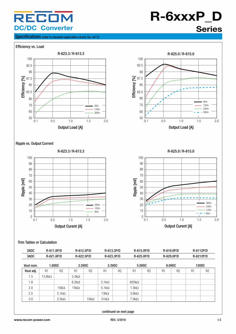
Efficiency vs. Load
Ripple vs. Output Current
R-623.3 / R-613.3
R-623.3 / R-613.3
50
70
60
82.5
87.5
85
90
100
92.5
80
Effic
ienc
y [%
]
Output Load [A]
0.1 0.5 1.0 1.5 2.0
9Vin12Vin26Vin
100
50
80
70
60
87.5
82.5
85
92.5
90
Effic
ienc
y [%
]Output Load [A]
0.1 0.5 1.0 1.5 2.0
9Vin12Vin24Vin38Vin
Ripp
le [m
V]
Output Curent [A]
0.1 0.5 1.0 1.5 2.0
38Vin24Vin12Vin9Vin
50
100
80
70
90
60
40
30
10
0
20
50
100
80
60
70
90
40
30
10
0
20
Ripp
le [m
V]
26Vin12Vin9Vin
Output Curent [A]
0.1 0.5 1.0 1.5 2.0
R-625.0 / R-615.0
R-625.0 / R-615.0
Trim Tables or Calculation
2ADC R-611.8P/D R-612.5P/D R-613.3P/D R-615.0P/D R-619.0P/D R-6112P/D
3ADC R-621.8P/D R-622.5P/D R-623.3P/D R-625.0P/D R-629.0P/D R-6212P/D
Vout nom. 1.8VDC 2.5VDC 3.3VDC 5.0VDC 9.0VDC 12VDC
Vout adj. R1 R2 R1 R2 R1 R2 R1 R2 R1 R2 R1 R2
1.5 13.6kΩ 3.3kΩ1.8 8.2kΩ 3.1kΩ 820kΩ2.0 10kΩ 15kΩ 5.1kΩ 1.5kΩ2.5 5.1kΩ 13kΩ 3.6kΩ3.0 2.5kΩ 10kΩ 51kΩ 7.0kΩ
continued on next page

www.recom-power.com REV.: 3/2018 I-4
DC/DC ConverterSpecifications (refer to standard application circuit, Ta= 25°C)
R-6xxxP_DSeries
REGULATIONSParameter Condition ValueOutput Accuracy ±1.0% typ. / ±2.0% max.
Line Regulation low line to high line, full load ±0.5% typ.
Load Regulation 10% to 100%, full loadR-61xxxR-62xxx
±0.5% max. ±1.0% max.
Transient Response (6)50% load step changeVout over / undershoot
100µs typ. / 200µs max.5% typ.
PROTECTIONSParameter Condition ValueShort Circuit Protection (SCP) continuous, automatic recovery
Short Circuit Input Current Vin > 12VDC 20mA typ. / 100mA max.
continued on next page
2ADC R-611.8P/D R-612.5P/D R-613.3P/D R-615.0P/D R-619.0P/D R-6112P/D
3ADC R-621.8P/D R-622.5P/D R-623.3P/D R-625.0P/D R-629.0P/D R-6212P/D
Vout nom. 1.8VDC 2.5VDC 3.3VDC 5.0VDC 9.0VDC 12VDC
Vout adj. R1 R2 R1 R2 R1 R2 R1 R2 R1 R2 R1 R2
3.3 1.7kΩ 5.9kΩ 9.7kΩ 0Ω 0Ω3.6 1.2kΩ 3.9kΩ 18kΩ 14kΩ 1.5kΩ 560Ω3.9 2.8kΩ 9.1kΩ 20kΩ 3.3kΩ 1.2kΩ4.5 1.6kΩ 3.9kΩ 60kΩ 7.5kΩ 2.1kΩ5.0 2.4kΩ 11kΩ 4.0kΩ5.1 2.2kΩ 60kΩ 12kΩ 4.3kΩ5.5 1.6kΩ 15kΩ 17kΩ 5.6kΩ6.0 1.1kΩ 7.2kΩ 24kΩ 7.5kΩ7.0 2.8kΩ 51kΩ 12kΩ8.0 1.5kΩ 130kΩ 19kΩ9.0 880Ω 31kΩ10 450Ω 36kΩ 55kΩ11 180Ω 15kΩ 125kΩ12 8.2kΩ13 4.7kΩ 11kΩ14 2.7kΩ 4.0kΩ15 1.3kΩ 1.6kΩ
Trim Tables or Calculation
Notes: Note6: Requires a 100µF electolytic or tantalum output capacitor for proper operation in all applications (the capacitor has to be placed as close as possible to the output pins)

www.recom-power.com REV.: 3/2018 I-5
DC/DC ConverterSpecifications (refer to standard application circuit, Ta= 25°C)
R-6xxxP_DSeries
ENVIRONMENTALParameter Condition Value Operating Temperature Range without derating @ natural convection 0.1m/s -40°C to +85°C
Maximum Case Temperature +110°C
Thermal Impedance @ natural convection 0.1m/s 25°C/W
Operating Humidity non-condensing 95% RH max.
Operating Altitude 2000m
Pollution Degree PD2
MTBF according to MIL-HDBK 217F, G.B.+25°C+71°C
563 x 103 hours117 x 103 hours
DIMENSION AND PHYSICAL CHARACTERISTICSParameter Type Value
Materialcase
pottingnon-conducive black plastic, (UL94 V-0)
epoxy, (UL94 V-0)
Package Dimension (LxWxH) 32.2 x 9.1 x 15.0mm
Package Weight 9g typ.
continue on next page
Optional Diode Protection Circuit
Add a blocking diode to Vout if current can flow backwards into the output, as this can damage the converter when it is powered down. Protection diodes are required for high capacitive loads.
The diode can either be fitted across the divice, if the source is low imped-ance or fitted in series with the output (recommended).
+Vout
GNDGND
+VinR-5/6/7xxx
+Vout
GND
Diode
Trim output voltageup to 1 diode drop
GND
+VinR-5/6/7xxx
Optional Protection 1: Optional Protection :
Output Soft Start
Innoline converters with Vadj pins (R-78AAxx-xxSMD, R-5xxx, R-6xxx and R-7xxx families) can be fitted with an external circuit to create an output soft start. Any general purpose PNP transistor and diode can be used for TR1 and D1 and typical values for R1 = 100K and C1 = 10µF. GND
Vcc
GNDCtrl
+Vin +Vout
Vadj
R1 D1
C1
TR1
On/Off
R-5/6/7xxx
SAFETY AND CERTIFICATIONSCertificate Type (Safety) Report / File Number Standard
Information Technology Equipment, General Requirements for Safety 1605077-12IEC60950-1:2005, 2nd Edition + AM2:2013
EN60950-1:2006 + AM2:2013
EAC RU-AT.49.09571 TP TC 004/2011
RoHs 2+ RoHS-2011/65/EU + AM-2015/863

www.recom-power.com REV.: 3/2018 I-6
DC/DC ConverterSpecifications (refer to standard application circuit, Ta= 25°C)
R-6xxxP_DSeries
Dimension Drawing (mm)
R-6xxxD
Pin Connections Pin # Single Description 1 ON / OFF Input pin: Active low (less than 0.8V) to disable the device 2,3,4 Vin Power Input 5, 6, 7, 8 GND Input and Output ground (common) 9, 10, 11 Vout Power output 12 Vout-Adj. With external resistors R1, R2 to selected output voltage
Tolerance: xx.x= ±0.5mm xx.xx= ±0.25mm
INSTALLATION AND APPLICATION
continued on next page
C1
2, 3, 4
Q1
1
5, 6, 7, 8
12
9, 10, 11
R1(Adjust down)
1µF(Optional)
R2(Adjust up)
C2100µF
ESR= 150mΩ max.(Required)
Vin
Com Com
VoutR-61xxR-62xxOFF
ON
TTL
Standard Application Circuit
Add blocking diode to Vout if current can flow backwards into the output, as this can damage the converter.(Please refer to “Optional Diode Protection Circuit” on Page I-5)
Bottom View
Top View1 2 3 4 5 6 7 8 9 10 11 121 2 3 4 5 6 7 8 9 10 11 12
2.54
2.54
9.132.2
11 x 2.54 = 27.94
0.8
0.70+0.10/-0.05 0.25±0.05
15.0
4.10
Marking
embossed logo
2.1
Bottom ViewTop View
1 2 3 4 5 6 7 8 9 10 11 12
1 2 3 4 5 6 7 8 9 10 11 12
2.54
2.54
32.2
15.0
9.1
17.0
2.1
11 x 2.54 = 27.94
0.70+0.10/-0.05 0.25±0.05
Recommended Footprint Details
Recommended Footprint Details
R-6xxxP

www.recom-power.com REV.: 3/2018 I-7
DC/DC ConverterSpecifications (refer to standard application circuit, Ta= 25°C)
R-6xxxP_DSeries
Positive to Negative Converter
Pin Connections Pin # Negative Out Positive Out 1 ON/OFF ON/OFF 2,3,4 +Vin +Viin 5, 6, 7, 8 -Vout GND 9, 10, 11 GND +Vout 12 -Vout-Adj +Vout-Adj
PACKAGING INFORMATIONParameter Type Value
Packaging Dimensions (LxWxH)R-6xxxDR-6xxxP
520.0 x 20.0 x 19.0mm530.0 x 23.0 x 19.0mm
Packaging Quantity tube 15pcs
Storage Temperature Range -40°C to +125°C
Bottom View
Top View1 2 3 4 5 6 7 8 9 10 11 121 2 3 4 5 6 7 8 9 10 11 12
2.54
2.54
9.132.2
11 x 2.54 = 27.94
0.8
0.70+0.10/-0.05 0.25±0.05
15.0
4.10
Marking
embossed logo
2.1
C2C1
2, 3, 4
1
5, 6, 7, 8
12
9, 10, 11
R1
Ref. to -Vout
R2
C1 and C2 are required and should be fitted close
to the converter pins.
+Vin
0V 0V
-Vout
On/Off
R-6xxP/D
The product information and specifications may be subject to changes even without prior written notice.The product has been designed for various applications; its suitability lies in the responsibility of each customer. The products are not authorized for use in safety-critical applications without RECOM’s explicit written consent. A safety-critical application is an application where a failure may reasonably be expected to endanger or cause loss of life, inflict bodily harm or damage property. The applicant shall indemnify and hold harmless RECOM, its affiliated companies and its representatives against any damage claims in connection with the unauthorized
use of RECOM products in such safety-critical applications.
Part Input Output Vout Output Efficiency Max. CapacitiveNumber Voltage Range Voltage Adjust Range (1) Current @ min Vin @ max. Vin Load (7)
[VDC] [VDC] [VDC] [A] [%] [%] C1 C2R-621.8 9 - 28 -1.8 -1.5~ -3.6 -1 72 65 10µF/50V 100µF/6.3VR-622.5 9 - 28 -2.5 -1.5~ -4.5 -1 76 72 10µF/50V 100µF/6.3VR-623.3 9 - 28 -3.3 -1.8~ -6 -1 79 76 10µF/50V 100µF/10VR-625.0 9 - 28 -5 -1.8~ -9 -1 81 80 10µF/50V 100µF/10VR-629.0 11 - 26 -9 -3.3~ -15 -0.8 84 85 10µF/50V 100µF/25VR-6212 11 - 26 -12 -3.3~ -15 -0.6 86 88 10µF/50V 100µF/25V
Selection Guide (Positive to Negativ)
Notes: Note7: Maximum capacitive load including C2 is 220µF