Embed Size (px)
Citation preview

© 2004 Xanoptix, Inc 1
Telecosm 2004
John Trezza
Telecosm 2004
John Trezza

© 2004 Xanoptix, Inc 2
Xanoptix PurposeXanoptix Purpose
Xanoptix exists to permit the concept of a “Chip”
to transcend materials, technologies and distances.
Xanoptix will enable a world free of hardware bottlenecks by allowing
unimpeded communication between integrated circuits
Many data paths,
Unrestricted speed, and
Vast reach (microns to kilometers).
By doing so, we will
Radically improve the price/performance electronics,
Merge ‘chips’ and ‘the network’, and
Move the IC industry from a ‘mainframe-like’ model to a ‘PC-like’ model.

© 2004 Xanoptix, Inc 3
More Complex Chips with More I/OMore Complex Chips with More I/O
1.E+001.E+011.E+021.E+031.E+041.E+051.E+061.E+071.E+081.E+091.E+101.E+111.E+121.E+131.E+141.E+15
1970 1980 1990 2000 2010
Year
Bit
Rat
e (M
egab
its/
seco
nd)
\
Off Chip Data
Data ON Chip
(Desired Data)
Stacked IC 10,000 x

© 2004 Xanoptix, Inc 4
Industry ProblemsIndustry Problems
ICs: Poor Communication & Performance•IN SYSTEM: Can send 0.01% of Desired CHIP Data
•BY USING 10% to 50% of CHIP POWER AND AREA
•IN NETWORK: 0.0001%
ICs:complex to design & Limited In Roadmap & Expensive•Material Choices Like the Model-T Colors •IP sharing hard•$1million & Months of Design for Each Attempt•No Upgradability•Large chips = “wafers-per-chip” Yields•Million costs when 90% of chip needs Inexpensive •Chips not expected to grow in next 10 years!
© 2004 Xanoptix, Inc 5
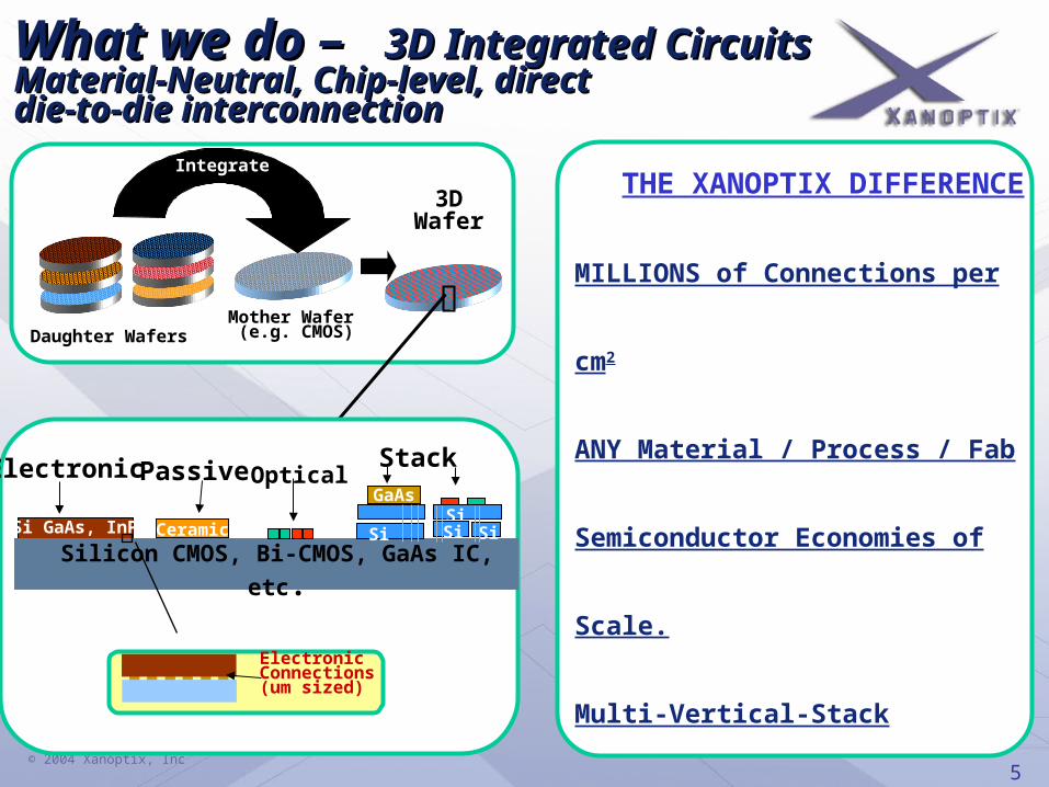
What we do – What we do – 3D Integrated Circuits3D Integrated CircuitsMaterial-Neutral, Chip-level, direct Material-Neutral, Chip-level, direct die-to-die interconnectiondie-to-die interconnection
3DWafer
Daughter WafersMother Wafer (e.g. CMOS)
Electronic
Si GaAs, InP
Silicon CMOS, Bi-CMOS, GaAs IC, etc.Ceramic
Passive
ElectronicConnections(um sized)
Optical
Si
GaAs
Stack
SiSi Si
THE XANOPTIX DIFFERENCE
MILLIONS of Connections per cm2
ANY Material / Process / Fab
Semiconductor Economies of Scale.
Multi-Vertical-Stack
1000s Optical Connections(Chips kilometers Apart Act as 1 Chip)
Integrate

© 2004 Xanoptix, Inc 6
Daughter IC
Mother Wafer
I/O Pad Openings
4 to 14um
7 to 50um
<5um
ProcessProcess
Multi-StackingChips w/ vias
Base ProcessElectrical, Mechanical,Thermal Connection

© 2004 Xanoptix, Inc 7
What we are working to achieveWhat we are working to achieve
Repeat the IC Revolution
Transform Boards of Chips & Modules
Into Individual Stacked Chips
USB/Audio/HDD
WLAN
GRAPHICS
PROCSSOR OPTICAL
DRAM
WLAN USB/Audio/HDD
WLAN
GRAPHICS
PROCSSOR OPTICAL
DRAM
WLAN USB/AudioHDD
WLAN
GRAPHICS
PROCSSOR
DRAM
WLAN

© 2004 Xanoptix, Inc 8
What we are working to achieveWhat we are working to achieve
Move the IC Industry from a ‘mainframe-like’ to
a ‘PC-like’ model
Transform Large, Complex Chips
Into Modular Stacked Chips
Processor CoreProcessor Core
L2 Cache Bus
Logic
L3 Cache
L3 CacheL3
CacheL3 Cache
Processor CoreProcessor Core
BusLogic
L2 Cache Processor
CoreProcessor Core
BusLogic
L3 CacheL3 CacheL3 CacheL2
Cache
Mainframe-Like PC-Like

© 2004 Xanoptix, Inc 9
What we are working to achieveWhat we are working to achieve
Remove I/O Bottlenecks over Any Distance.
Transform Many ICs & the network
IntoOne Big ‘Chip’
Silicon CMOS IC(e.g. Microprocessor)
SRAM Mixed Signal IC RF Chip
Optical I/ODRAM
Silicon CMOS IC(e.g. Microprocessor)
SRAM Mixed Signal IC RF Chip
Optical I/ODRAM
Kilometers
MicronsTransceiver

© 2004 Xanoptix, Inc 10
3D Stacked 3D Stacked ICs:ICs:
ICs are Dramatically Improved in Performance
•ALL Data Available over ANY distance (The chip =network)•90% Less I/O Power•99% Less I/O Space
ICs are Unlimited in Flexibility & Decreased in Cost•Mix & Match Processes & Material From Best Suppliers •The chip IS the board•Days of Design for new version of a chip •Customize & Upgrade your chip just a PC.•Several Smaller chips each with very high yield •Cost is on function-by Function basis
•‘Unlimited’ chip size

© 2004 Xanoptix, Inc 11
Key CapabilitiesKey Capabilities
Optical Device Design
& Fabrication Mixed Signal
IC Design
Optical Packaging Design3-D Folded
Packaging Design
ELECTRONICS OPTICS3D Stacked IC

© 2004 Xanoptix, Inc 12
Xanoptix Has Advanced 3D CapabilitiesXanoptix Has Advanced 3D Capabilities
1st Optical
ProductElectrical Chips
Demonstrated Chips for Products
Capability
# contacts/chi
p~ 600 10,000 Million Million+
Contact Size 14 um 7 um 4 um 2 umContact Density 40,000/cm2 160,000 / cm2 1,000,000/cm2 1,000,000+/ cm2
# Optical devices 216 N/A ~ 300,000 > 300,000
Contact yields 99.9995%

© 2004 Xanoptix, Inc 13
Single Chip Optoelectronic Transceiver 250 Gb/s
(equivalent to 1,250 Ethernet Cards)
Combines active optics and electronics into single chips
First Commercial ApplicationFirst Commercial Application

© 2004 Xanoptix, Inc 14
Para-Optix Product LinePara-Optix Product Line
Chip Heat SinkOptical
Connector Electrical Connector
P R O G R A M M I N G
XTM-12 XTM-16 XTM-24 XTM-32 XTM-48 XTM-72
Xanoptix IC
Xanoptix Component
•15x number of optical devices•3:1 Laser redundancy•Programmable
Xanoptix3-D
Packaging
1cmOptical Output
5Gb/s 400Gb/s

© 2004 Xanoptix, Inc 15
PARA-OPTIX VS. LC SFFPARA-OPTIX VS. LC SFF
IP Routers
Core Switching
CATV/Metro Switching
Storage/Data Switching
Computing & Server

© 2004 Xanoptix, Inc 16
Next Generation: Next Generation: Fiber CablesFiber Cables
NEXT GENERATION PASSIVE NEXT GENERATION PASSIVE OPTICAL CABLING OPTICAL CABLING
““100,000 points of light100,000 points of light” ”
3mm
100,000 fibers
1000s Optical I/O
100,000s of fibers

© 2004 Xanoptix, Inc 17
Future Development RoadmapsFuture Development Roadmaps
Tx / RxTransceiverBackup/redundancy Power monitoringPre-EmphasisEqualization SERDESClock RecoveryMicroprocessorFPGAGraphicsNetwork Processors SRAM &DRAMBIOS ChipsetsMemory controllersDrive controllersData aggregatorsMicroprocessorsGbE / FibCh codecSONET scramblingCrossbar SwitchingDrop/AddECC & CRCRegenerators FramingHeader DecodingDigital CrossconnectWDM CrossconnecctClocking distributionBus Controller
850nm VCSEL
1310nm DFB
Single Mode devices
CWDM (2-16 )
1550nm DFB
DWDM(16-256+ )
600nm VCSEL
1310nm VCSEL
640 Mb/s/ch
1 Gb/s/ch
1.25 Gb/s/ch
2.5 Gb/s/ch
3.125 Gb/s/ch
5.5 Gb/s/ch
6.25 Gb/s/ch
10 Gb/s/ch
12.5 Gb/s/ch
40 Gb/s/ch
Intelligence Speed/I/O Wavelength(s)1248
12162432487296
128144256288576
921636864
589824
# optical I/O

© 2004 Xanoptix, Inc 18
Microprocessor, Router,DWDM System
• 1000s of Optical I/O channels• Hundreds of wavelengths
Expensive Monolithic
Routers, Servers,DWDM systems
CommoditySystems
BECOME
Example: Communication SystemsExample: Communication Systems
$1 Million ; 6ft System. $1,000 ; 1in System.

© 2004 Xanoptix, Inc 19
Silicon CMOS IC(e.g. Microprocessor)
SRAM Mixed Signal IC RF Chip
Optical I/ODRAM
Silicon CMOS IC(e.g. Microprocessor)
SRAM Mixed Signal IC RF Chip
Optical I/ODRAM
Kilometers
MicronsTransceiver

© 2004 Xanoptix, Inc 20
Computing, Storage, Office, and Computing, Storage, Office, and Consumer OpportunitiesConsumer Opportunities
Other Consumer Electronics•Single Chip DVD Recorder (read the disk in one rotation)•Memory Stacks•Single chip “Xbox in a wristwatch”•Printer/Scanner/Copier Chip
Highly Parallel Communication For storage systems
Single Chip Digital Cameras(Sensor, Logic, Memory, display, and Network in one)

© 2004 Xanoptix, Inc 21
Next Generation:Next Generation:Telecom & Communications ProductsTelecom & Communications Products
LNB devices/Modules for Satellite TV
Single Chip Fiber to The Home ‘box’
WLAN on a Chip
Cell Phone / Base Station “on a Chip”
Single-Chip, Ultra Redundant Undersea Repeaters
Modular ASICs

© 2004 Xanoptix, Inc 22
Next Generation:Next Generation:Consumer, Industrial, Military, and CommercialConsumer, Industrial, Military, and Commercial
Avionics & Space
The Connector/Cable *IS* the Electronics/Optics/network
In-Flight Networking & Entertainment Chips
Single Chip High-Temp Industrial Control Sytems
Active printed circuit boards, Cables & IC sockets
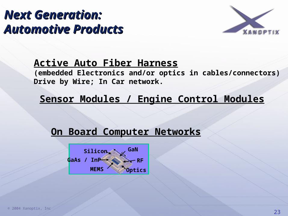
© 2004 Xanoptix, Inc 23
Active Auto Fiber Harness(embedded Electronics and/or optics in cables/connectors)Drive by Wire; In Car network.
Next Generation:Next Generation:Automotive ProductsAutomotive Products
Sensor Modules / Engine Control Modules
On Board Computer Networks
Silicon
GaAs / InP
GaN
RF
OpticsMEMS
© 2004 Xanoptix, Inc 24
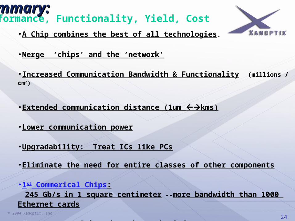
•A Chip combines the best of all technologies.
•Merge ‘chips’ and the ‘network’
•Increased Communication Bandwidth & Functionality (millions / cm2)
•Extended communication distance (1um kms)
•Lower communication power
•Upgradability: Treat ICs like PCs
•Eliminate the need for entire classes of other components
•1st Commerical Chips: 245 Gb/s in 1 square centimeter --more bandwidth than 1000 Ethernet cards
•Huge opportunities throughout the industry.
Summary:Summary:Performance, Functionality, Yield, Cost

© 2004 Xanoptix, Inc 25
The VisionThe Vision
Integrated Circuits
Developed (1961)(TI & Fairchild)
Event Significance First Product Market Result
RevolutionizedElectronics
Hearing Aid $100s Billions
Electronics industry
now
3D andOPTICALLY
ENABLEDIntegrated
CircuitsDeveloped (2001)
(Xanoptix)
RevolutionizesElectronics & The Network
Intelligent Transceiver $