Embed Size (px)
Citation preview

ELEN 146
1
1 Amplifier Frequency Response Signal frequency has a pronounced effect on the response of amplifiers. In past analysis of circuits, we have assumed our capacitors to have 0 Ω of reactance to our ac signals, and infinite Ω of reactance to DC signals. (i.e., shorts for AC and opens for DC). The actual reactance of the capacitors is dependant on the frequency of the signal:
fCX c π2
1= As frequency increase, Xc decreases.
Now, we need to take a closer look at amplifier circuits to see the affects capacitors have on performance of amps at different frequencies.
1.1 Effects of External Capacitors Take this common emitter circuit:
Input The input circuit looks like this:

ELEN 146
2
And when simplified:
If we consider C1 as a short, then
gengin
inin v
RZZ
v ×+
=
But, if we take the reactance of C1 into consideration (fC
X c π21
= ) then:
gencgin
inin v
XRZZ
v ×++
=
As frequency decreases, Xc increases and so the vin decreases and so does vout.
Output The output looks like this:
ELEN 146
3
If C3 is a short, vout = vc, but in reality, we have the reactance of C3 included.
So, 3CL
Lcout XR
Rvv+
×=
As frequency decreases, Xc increases, therefore, vout again decreases.
Due to the coupling capacitors at the input and the output, the output amplitude of our amplifier is decreased as the frequency of the input signal decreases.
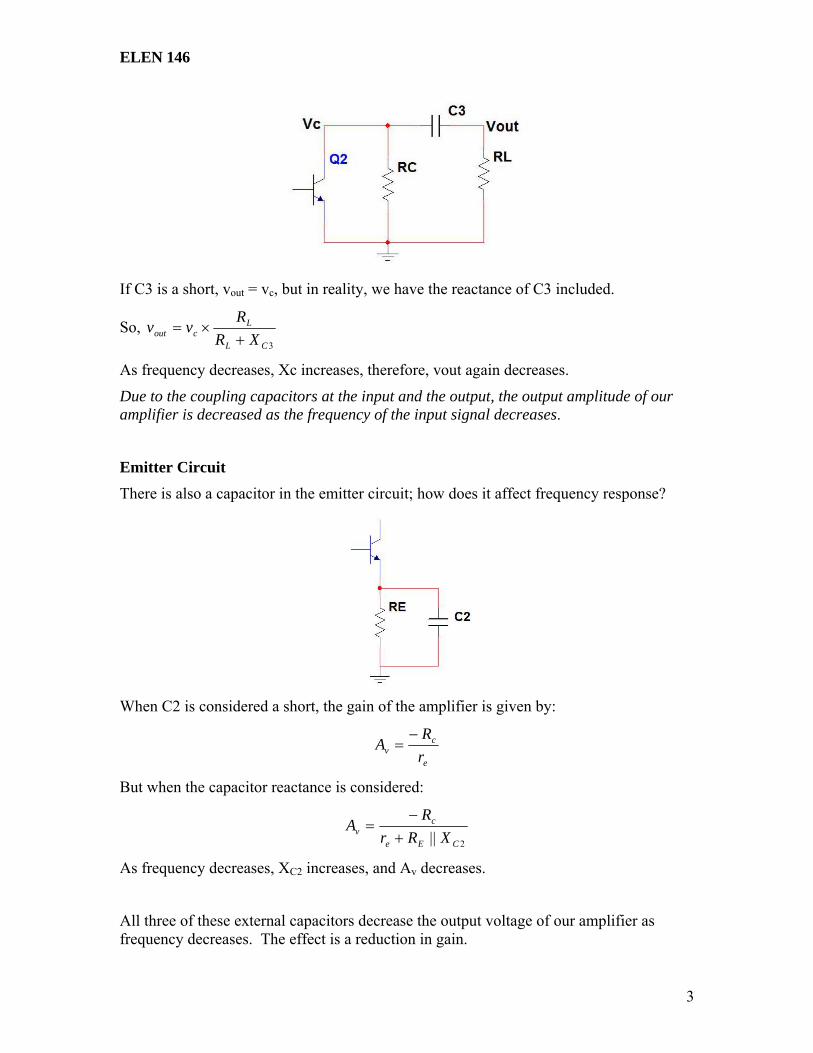
Emitter Circuit There is also a capacitor in the emitter circuit; how does it affect frequency response?
When C2 is considered a short, the gain of the amplifier is given by:
e
cv r
RA
−=
But when the capacitor reactance is considered:
2|| CEe
cv XRr
RA
+−
=
As frequency decreases, XC2 increases, and Av decreases.
All three of these external capacitors decrease the output voltage of our amplifier as frequency decreases. The effect is a reduction in gain.

ELEN 146
4
1.2 Internal Transitor Capacitance Capacitance is found anytime you have two adjacent, but separated charged items. This effect is sometimes useful, but very often is a side effect of having two conductors close together. Capacitance of this kind is called stray or parasitic capacitance, and it can have undesirable effects in the system.
Stray capacitance is found between the base and collector of a BJT, as well as between the base and emitter.
Cbc is the base-collector junction capacitance and is referred to as the output capacitance (Cob).
Cbe is the base-emitter junction capacitance and is referred to as the input capacitance (Cib).
These capacitances are very small (only a few picofarads) and therefore at low frequencies, Xc is very high and the capacitance will appear as an open circuit. As frequencies go up, this reactance becomes smaller and at some point, the reactance begins to have an effect on transistor performance.
Effect of Cbe
As frequency increases, Xcbe decreases, and we get a significant voltage divider, and the actual vin to the base of the transistor decreases.
Effect of Cbc
ELEN 146
5
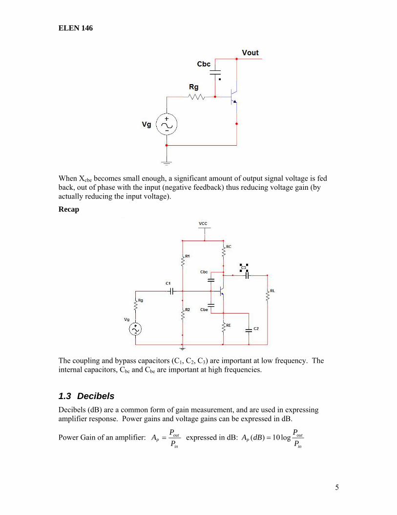
When Xcbe becomes small enough, a significant amount of output signal voltage is fed back, out of phase with the input (negative feedback) thus reducing voltage gain (by actually reducing the input voltage).
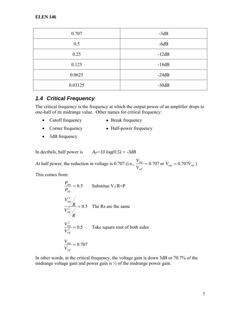
Recap
The coupling and bypass capacitors (C1, C2, C3) are important at low frequency. The internal capacitors, Cbc and Cbe are important at high frequencies.
1.3 Decibels Decibels (dB) are a common form of gain measurement, and are used in expressing amplifier response. Power gains and voltage gains can be expressed in dB.
Power Gain of an amplifier: in
outP P
PA = expressed in dB:
in
outP P
PdBA log10)( =

ELEN 146
6
Voltage Gain of an amplifier: in
outV V
VA = expressed in dB:
in
outV V
VdBA log20)( =
Be careful with the phase relationship of the gain – if you have an inverting amplifier with a gain of AV=-175, it would not be expressed as 20log(-175)=-44.86. It would be expressed as 20log(175)=44.86 and 180° out of phase.
1.3.1 0 dB Reference Up until now, our analysis of amplifiers has considered amplifiers operating in the “Midrange” or “midband” of frequencies. This is the range of frequencies where we can consider the coupling and bypass capacitors to appear as short circuits (XC≈0) and conversely, we can consider the internal capacitors to appear as open circuits (XC≈∞). The gain of an amplifier in the midrange is at the maximum it can be.
Decibels are always measured with respect to something, and usually that selection of “something” can be arbitrary. For frequency analysis, we can use the midrange gain as the reference point, and assign it a value of 0dB. In an amplifier, any value of gain below the midrange gain can be referenced to this 0dB point and is expressed as a negative dB value.
Example: If the amplifier midrange voltage gain is 100, and the gain at a certain frequency below the midrange is 50, this reduced gain can be expressed as:
dB65.0log2010050log20 −==
This means that the gain is 6dB below the reference level of 0dB.
• Halving the output voltage for a fixed input voltage is a 6dB reduction in gain
• Doubling the output voltage for a fixed input voltage is a 6dB increase in gain.
The following is a table of absolute and relative voltage gains in dB
Absolute Voltage Gain Voltage Gain in dB
32 30dB
16 24dB
8 18dB
4 12dB
2 6dB
1 0dB
ELEN 146
7
0.707 -3dB
0.5 -6dB
0.25 -12dB
0.125 -18dB
0.0625 -24dB
0.03125 -30dB
1.4 Critical Frequency The critical frequency is the frequency at which the output power of an amplifier drops to one-half of its midrange value. Other names for critical frequency:
• Cutoff frequency Break frequency
• Corner frequency Half-power frequency
• 3dB frequency
In decibels, half power is AP=10 log(0.5) = -3dB
At half power, the reduction in voltage is 0.707 (i.e., 707.0=ref
out
VV
or refout VV 707.0= )
This comes from:
5.0=ref
out
PP
Substitue V2/R=P
5.02
2
=
RV
RV
ref
out
The Rs are the same
5.02
2
=ref
out
VV
Take square root of both sides
707.0=ref
out
VV
In other words, at the critical frequency, the voltage gain is down 3dB or 70.7% of the midrange voltage gain and power gain is ½ of the midrange power gain.

ELEN 146
8
1.5 Analyzing Low Frequency Amplifier Response Common Emitter Amplifier as we’ve seen many times…capacitively coupled
In this circuit there are three high-pass RC circuits that affect the gain as frequency is reduced below midrange.
1. The input RC high-pass circuit
2. The output RC high-pass circuit
3. The emitter RC high-pass circuit
ELEN 146
9
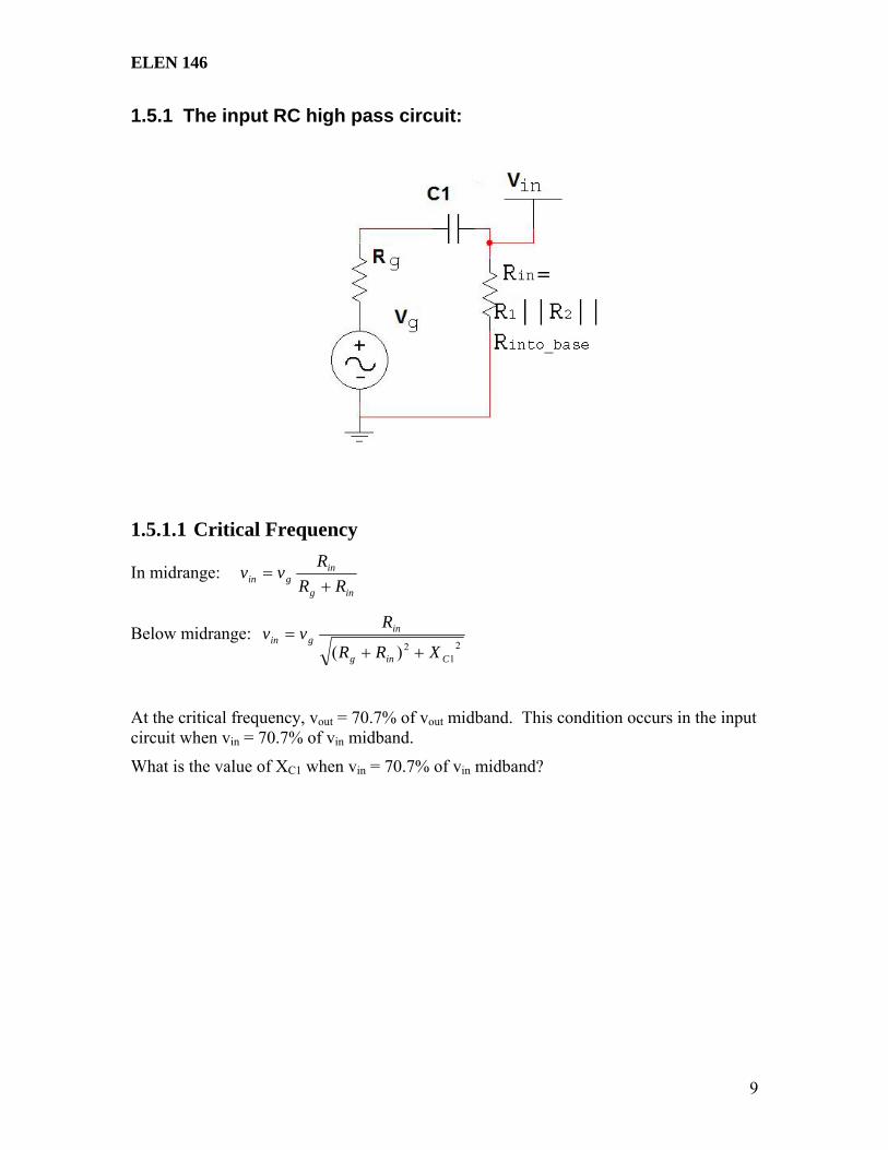
1.5.1 The input RC high pass circuit:
1.5.1.1 Critical Frequency
In midrange: ing
ingin RR
Rvv
+=
Below midrange: 2
12)( Cing
ingin
XRR
Rvv
++=
At the critical frequency, vout = 70.7% of vout midband. This condition occurs in the input circuit when vin = 70.7% of vin midband.
What is the value of XC1 when vin = 70.7% of vin midband?
ELEN 146
10
So, the 3dB point occurs when XC1 = Rg + Rin.
Also, since fC
X c π21
= ,
fCRR ing π2
1=+ and solving for frequency:
1)(21
CRRf
ingcutoff +
=π
1.5.1.2 Voltage Gain Roll-Off at Low Frequencies
As frequency decreases below the critical frequency, the overall voltage gain continues to decrease. This decrease is called the Roll-Off.
What is the rate of roll-off?
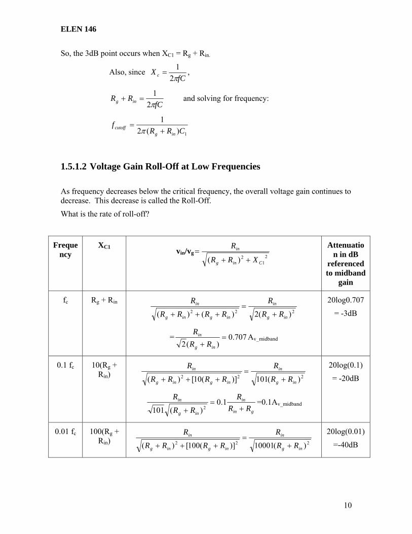
Frequency
XC1 vin/vg2
12)( Cing
in
XRR
R
++=
Attenuation in dB
referenced to midband
gain
fc Rg + Rin 222 )(2)()( ing
in
inging
in
RR
R
RRRR
R
+=
+++
= 707.0)(2=
+ ing
in
RRR
Av_midband
20log0.707
= -3dB
0.1 fc 10(Rg + Rin) 222 )(101)](10[)( ing
in
inging
in
RR
R
RRRR
R
+=
+++
gin
in
ing
in
RRR
RR
R+
=+
1.0)(101 2
=0.1Av_midband
20log(0.1)
= -20dB
0.01 fc 100(Rg + Rin) 222 )(10001)](100[)( ing
in
inging
in
RR
R
RRRR
R
+=
+++
20log(0.01)
=-40dB

ELEN 146
11
gin
in
ing
in
RRR
RR
R+
=+
01.0)(10001 2
=
0.01Av_midband
0.001 fc 1000(Rg + Rin) 2622 ))(110()](1000[)( ing
in
inging
in
RR
R
RRRR
R
++=
+++
gin
in
ing
in
RRR
RR
R+
=+
001.0)(1000001 2
=
0.001Av_midband
20log(0.01)
=-60dB
After spending some time studying the equations in the above table, you should be able to come to the conclusion that for each 10 times reduction in frequency below fc, there is a 20dB reduction in the voltage gain. This rate of change is the roll-off. Since a ten times change in frequency is called a diode, we say that the roll-off of this amplifier due to the input RC circuit is:
-20dB/decade This roll-off can also be plotted in the format of dB voltage gain versus frequency in a plot called a Bode Plot.

ELEN 146
12
Sometimes roll-off of an amplifier is expressed in dB/octave instead of dB/decade. An octave is changing the frequency by a factor of 2 (i.e., doubling or halving). Therefore, a rate of -20dB/decade ≈ -6dB/octave.
1.5.1.3 Phase Shift in Input RC Circuit The input RC circuit also introduces an increasing phase shift through the amplifier as frequency decreases.
At midrange, the phase shift is ≈0 because the XC is ≈0. At lower frequencies, the phase shift increases, because XC increases. Therefore, the output voltage of the RC circuit leads the generator voltage.
The phase angle, θ is:
⎟⎟⎠
⎞⎜⎜⎝
⎛
+= −
gin
C
RRX 11tanθ
You can see this graphically in the following diagram:
In the case of a series RC circuit, the voltage across the resistance leads the voltage across the impedance Z.
At midrange, XC ≈ 0 … 00tan0tan 11 ==⎟⎟⎠
⎞⎜⎜⎝
⎛
+= −−
gin RRθ
At fc, XC=Rin+Rg … 451tantan 11 ==⎟⎟⎠
⎞⎜⎜⎝
⎛
+
+= −−
gin
gin
RRRR
θ
ELEN 146
13
At f= 0.1fc, XC=10(Rin+Rg) … 3.8410tan)(10
tan 11 ==⎟⎟⎠
⎞⎜⎜⎝
⎛
+
+= −−
gin
gin
RRRR
θ
As frequency approaches 0 Hz, the phase shift approaches 90°. The phase angle can also be plotted against frequency as we can see in the following diagram.
That demonstrates how one of the high-pass RC circuits affects amplifier operation. Now, let’s look at the other two.
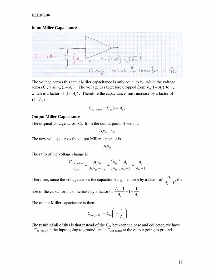
1.5.2 Output RC high-pass circuit:
We can assume the input to the collector is an open circuit, therefore, the critical frequency for this circuit is determined by C3, RC, and RL. As frequency decreases, more of the collector voltage (VC) is dropped across XC, and less across RL, therefore vout must decrease.

ELEN 146
14
1)(21
CRRf
LCcutoff +
=π
At this frequency, the output voltage is reduced by a factor of 0.707 from midrange level, which corresponds to a reduction in voltage gain of 3dB.
The phase shift in the output RC circuit is:
⎟⎟⎠
⎞⎜⎜⎝
⎛+
= −
LC
C
RRX 31tanθ
At the cutoff frequency, XC3 = RC + RL and therefore: ( ) 451tan 1 == −θ
1.5.3 The Emitter Bypass Circuit
As frequency decreases, XC2 increases, and therefore RE is no longer bypassed by a 0Ω resistor. The voltage gain then decreases, since it is:
Ee
Cv Rr
RA
+−=
The resistance that the capacitor sees (Thevenin resistance) is
)||||(|| 21 geE RRRrR +
The cutoff frequency is then:

ELEN 146
15
221 )||||(||(21
CRRRrRf
geEcutoff +
=π
And the phase angle is:
⎟⎟⎠
⎞⎜⎜⎝
⎛
+= −
)||||(tan
21
31
ge
C
RRRrX
θ
1.5.4 Combined Effect of All High Pass Components The combined effect of all three of these RC circuits on the amplifier makes the frequency response at low frequencies more dramatic than you would expect from just one RC circuit. The critical frequency of each circuit is usually not the same. If one of the circuits has a critical frequency higher than the other two, then it is the dominant, or highest frequency cutoff that determines the voltage at which overall voltage gain of amp begins to drop at -20dB/decade.
The other circuits of course contribute to the gain at their appropriate corner frequency:

ELEN 146
16
Below the midrange, the input RC circuits causes vin to lead vg by the circuit phase angle:
1.6 High Frequency Response
Cbc connects output to input of the inverting amp and provides negative feedback as frequency increases and Xcbc decreases. Both the input voltage and output voltage are changed and the effect is difficult to directly analyze.

ELEN 146
17
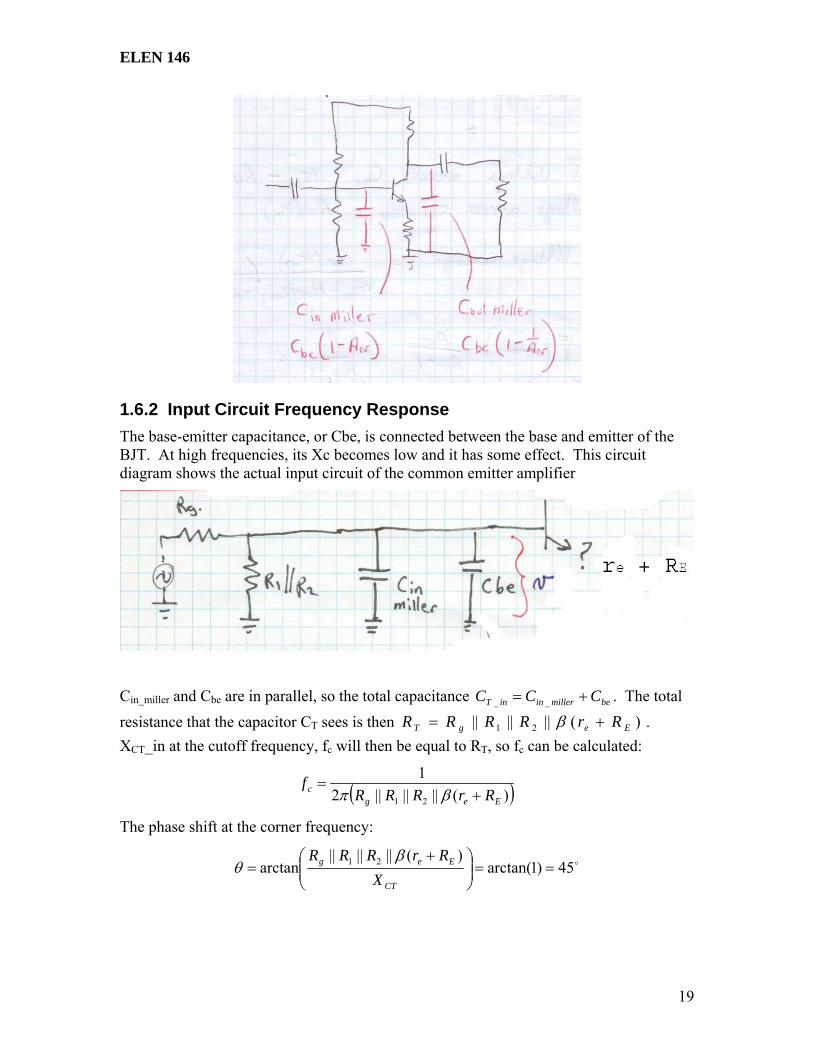
1.6.1 Cbc and Miller’s Theorem A simple way to model and analyze the impact of these capacitances at high frequency is to take the Cbc connecting input and output, and split it into two capacitances going to ground:
one at the input the Cin_miller = Cbc(1-Av)
at the output Cout_miller.=(Cbc(1-1/ Av))
Why can we do this? The total voltage drop across Cbc = vin – vout = vin – (Av* vin):
Alternatively:
)1( vinbc AvC −=
The charge stored on the capacitor is:
( )[ ]vin AvCCVQ −== 1
When we move the capacitor to a “Miller Equivalent” (i.e., input and output), we must still satisfy the Q=CV relationship of the original capacitor to model the effect of the capacitor properly.
ELEN 146
18
Input Miller Capacitance
The voltage across this input Miller capacitance is only equal to vin. while the voltage across Cbc was )1( vin Av − . The voltage has therefore dropped from )1( vin Av − to vin
which is a factor of )1( vA− . Therefore the capacitance must increase by a factor of )1( vA− :
)1(_ vbcmillerin ACC −=
Output Miller Capacitance The original voltage across Cbc from the output point of view is:
ininv vvA −
The new voltage across the output Miller capacitor is
invvA
The ratio of the voltage change is
11_
−=
−⎟⎟⎠
⎞⎜⎜⎝
⎛=
−=
v
v
v
v
in
in
ininv
inv
bc
millerout
AA
AA
vv
vvAvA
CC
Therefore, since the voltage across the capacitor has gone down by a factor of 1−v
v
AA
, the
size of the capacitor must increase by a factor of vv
v
AAA 111
−=−
The output Miller capacitance is then:
⎟⎟⎠
⎞⎜⎜⎝
⎛−=
vbcmillerout A
CC 11_
The result of all of this is that instead of the Cbc between the base and collector, we have a Cin_miller at the input going to ground, and a Cout_miller at the output going to ground.
ELEN 146
19
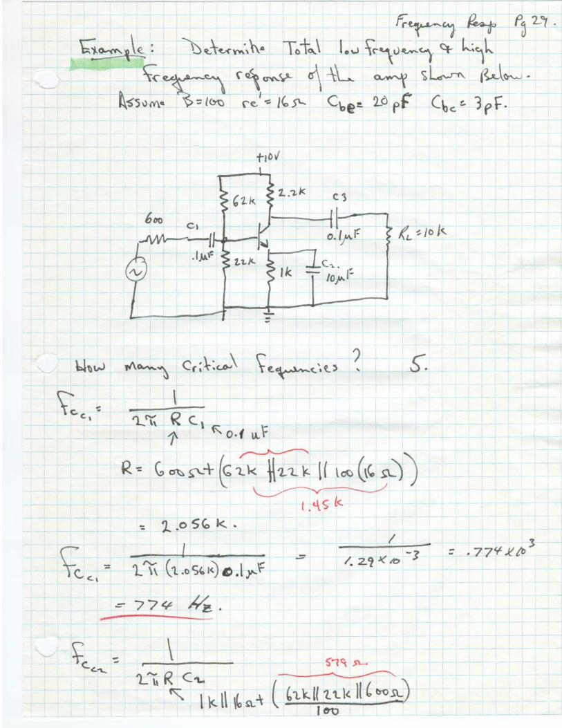
1.6.2 Input Circuit Frequency Response The base-emitter capacitance, or Cbe, is connected between the base and emitter of the BJT. At high frequencies, its Xc becomes low and it has some effect. This circuit diagram shows the actual input circuit of the common emitter amplifier
Cin_miller and Cbe are in parallel, so the total capacitance bemillerininT CCC += __ . The total resistance that the capacitor CT sees is then )(|||||| 21 EegT RrRRRR += β . XCT_in at the cutoff frequency, fc will then be equal to RT, so fc can be calculated:
( ))(||||||21
21 Eegc RrRRR
f+
=βπ
The phase shift at the corner frequency:
45)1arctan()(||||||
arctan 21 ==⎟⎟⎠
⎞⎜⎜⎝
⎛ +=
CT
Eeg
XRrRRR β
θ

ELEN 146
20
1.6.3 Output Circuit Frequency Response The output circuit with the output Miller capacitance is shown in this diagram:
The Miller capacitor sees RC||RL, and therefore, the corner frequency for the output circuit is:
MilleroutLcc CRR
f_)||(2
1π
=
And
⎟⎟⎠
⎞⎜⎜⎝
⎛=
MilleroutC
LC
XRR
__
||arctanθ
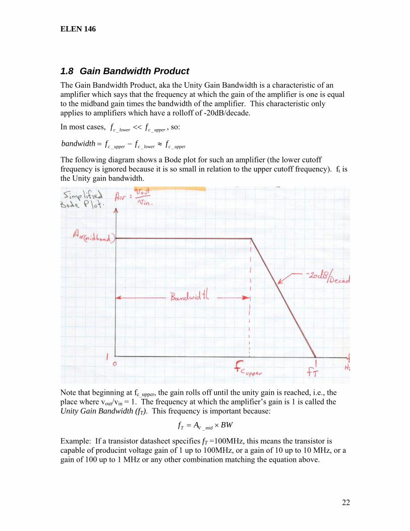
1.7 Total Amplifier Frequency Response The total amplifier frequency response must take into account both the upper and lower frequency responses. The following diagram shows an example Bode plot of an amplifier frequency response:

ELEN 146
21
The bandwidth of this amplifier is the range of frequencies between the lower cutoff frequency, and the upper cutoff frequency:
lowercupperc ffbandwidth __ −=

ELEN 146
22
1.8 Gain Bandwidth Product The Gain Bandwidth Product, aka the Unity Gain Bandwidth is a characteristic of an amplifier which says that the frequency at which the gain of the amplifier is one is equal to the midband gain times the bandwidth of the amplifier. This characteristic only applies to amplifiers which have a rolloff of -20dB/decade.
In most cases, upperclowerc ff __ << , so:
upperclowercupperc fffbandwidth ___ ≈−=
The following diagram shows a Bode plot for such an amplifier (the lower cutoff frequency is ignored because it is so small in relation to the upper cutoff frequency). ft is the Unity gain bandwidth.
Note that beginning at fc_upper, the gain rolls off until the unity gain is reached, i.e., the place where vout/vin = 1. The frequency at which the amplifier’s gain is 1 is called the Unity Gain Bandwidth (fT). This frequency is important because:
BWAf midVT ×= _
Example: If a transistor datasheet specifies fT =100MHz, this means the transistor is capable of producint voltage gain of 1 up to 100MHz, or a gain of 10 up to 10 MHz, or a gain of 100 up to 1 MHz or any other combination matching the equation above.
ELEN 146
23
Example: If fT =175MHz and AV_mid = 50. What is the bandwidth of the amplifier?
Since BWAf midVT ×= _ , then midV
TA
fBW_
= . BW = 175MHz/50 = 3.5 MHz.
1.9 Bandwidth of Cascaded Amplifiers The overall bandwidth of cascaded amplifiers is less than the bandwidth of any one stage. If two identical stages each have a bandwidth of 10kHz, then for one stage, the response would be down 3dB but for the two stages together, the response is down 6dB.
The overall bandwidth of n identical stages is:
121
−= nn BWBW
So, going back to the two 10kHz bandwidth stages, the combined response is:
( ) kHzkHzkHzBW 43.61414.1101210 21
=−=−=
This effect is referred to as the bandwidth shrinkage. Remember even if the bandwidth of each stage is different, the overall BW of cascaded stages will be smaller than the smallest bandwidth of any stage.
Bandwidth shrinkage is a result of the overall reduction of the upper cutoff frequency and increasing of the lower cutoff frequency:
121
_ −= nupperuppern ff
12
11_
−
=n
lowerlowern ff