Embed Size (px)
Citation preview
1
ATD10B8CV2 on MC9SI2CBy: Yuchun Huang

2
ADC
ADC Power Supply
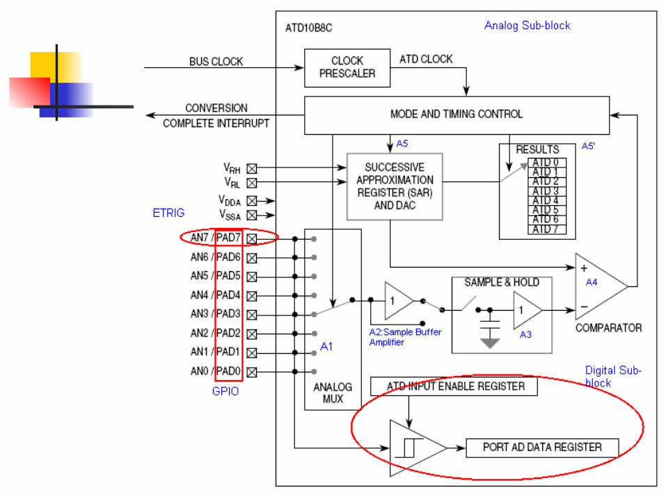
3
4
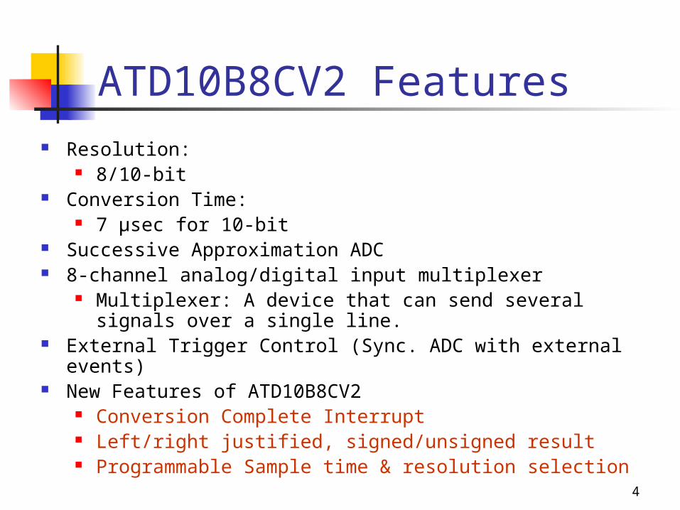
ATD10B8CV2 Features Resolution:
8/10-bit Conversion Time:
7 µsec for 10-bit Successive Approximation ADC 8-channel analog/digital input multiplexer
Multiplexer: A device that can send several signals over a single line.
External Trigger Control (Sync. ADC with external events) New Features of ATD10B8CV2
Conversion Complete Interrupt Left/right justified, signed/unsigned result Programmable Sample time & resolution selection
5
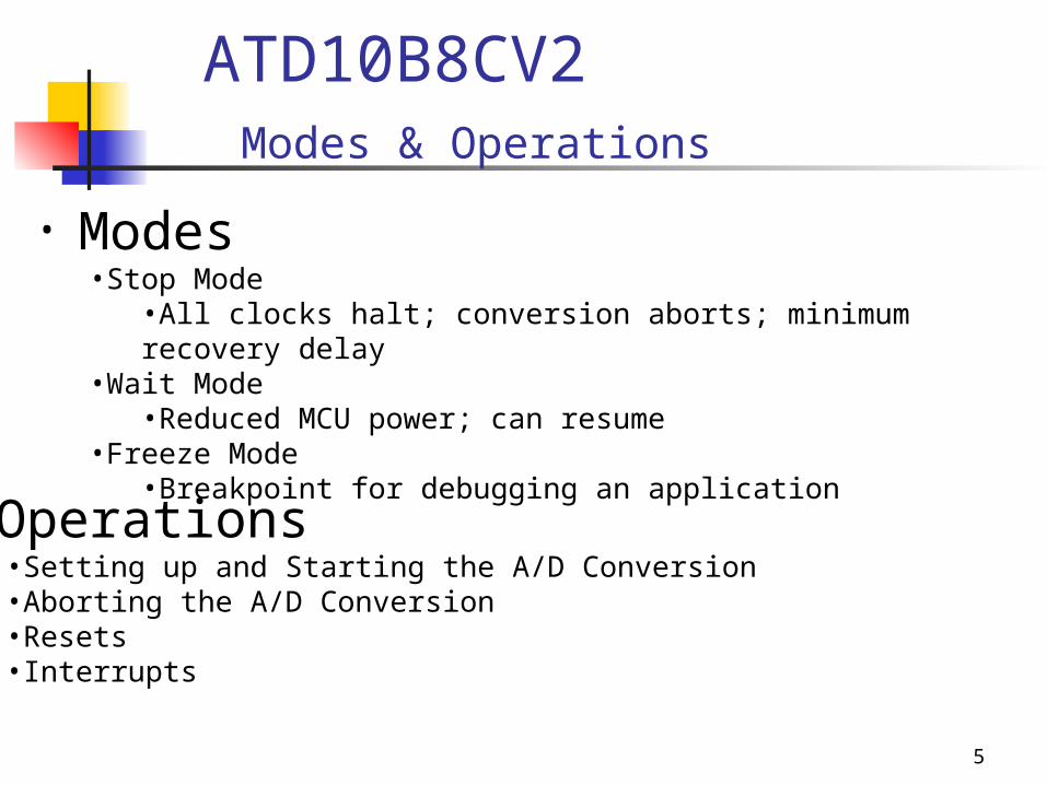
• Operations•Setting up and Starting the A/D Conversion•Aborting the A/D Conversion•Resets•Interrupts
ATD10B8CV2 Modes & Operations
• Modes•Stop Mode
•All clocks halt; conversion aborts; minimum recovery delay•Wait Mode
•Reduced MCU power; can resume•Freeze Mode
•Breakpoint for debugging an application
6
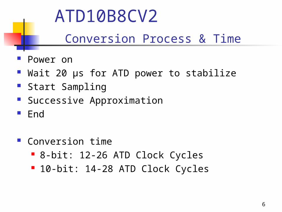
ATD10B8CV2 Conversion Process & Time
Power on Wait 20 μs for ATD power to stabilize Start Sampling Successive Approximation End
Conversion time 8-bit: 12-26 ATD Clock Cycles 10-bit: 14-28 ATD Clock Cycles
7
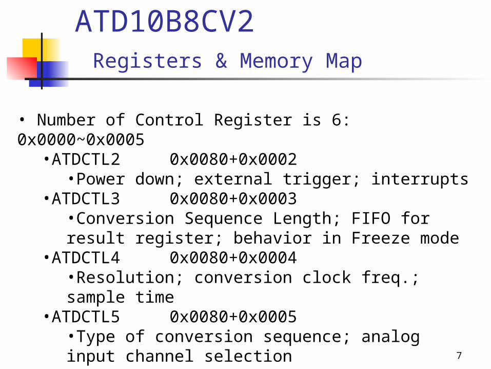
ATD10B8CV2 Registers & Memory Map
• Number of Control Register is 6: 0x0000~0x0005•ATDCTL2 0x0080+0x0002
•Power down; external trigger; interrupts•ATDCTL3 0x0080+0x0003
•Conversion Sequence Length; FIFO for result register; behavior in Freeze mode
•ATDCTL4 0x0080+0x0004•Resolution; conversion clock freq.; sample time
•ATDCTL5 0x0080+0x0005•Type of conversion sequence; analog input channel selection
8
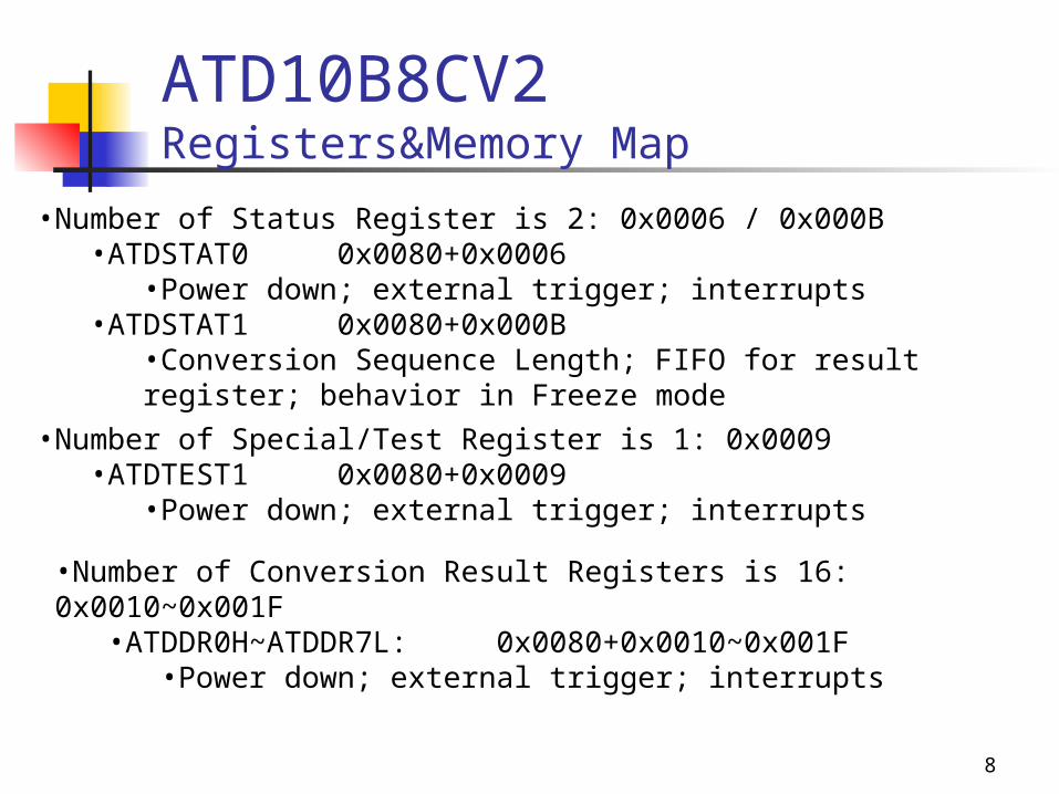
ATD10B8CV2 Registers&Memory Map
•Number of Status Register is 2: 0x0006 / 0x000B•ATDSTAT0 0x0080+0x0006
•Power down; external trigger; interrupts•ATDSTAT1 0x0080+0x000B
•Conversion Sequence Length; FIFO for result register; behavior in Freeze mode
•Number of Special/Test Register is 1: 0x0009•ATDTEST1 0x0080+0x0009
•Power down; external trigger; interrupts
•Number of Conversion Result Registers is 16: 0x0010~0x001F•ATDDR0H~ATDDR7L: 0x0080+0x0010~0x001F
•Power down; external trigger; interrupts
9
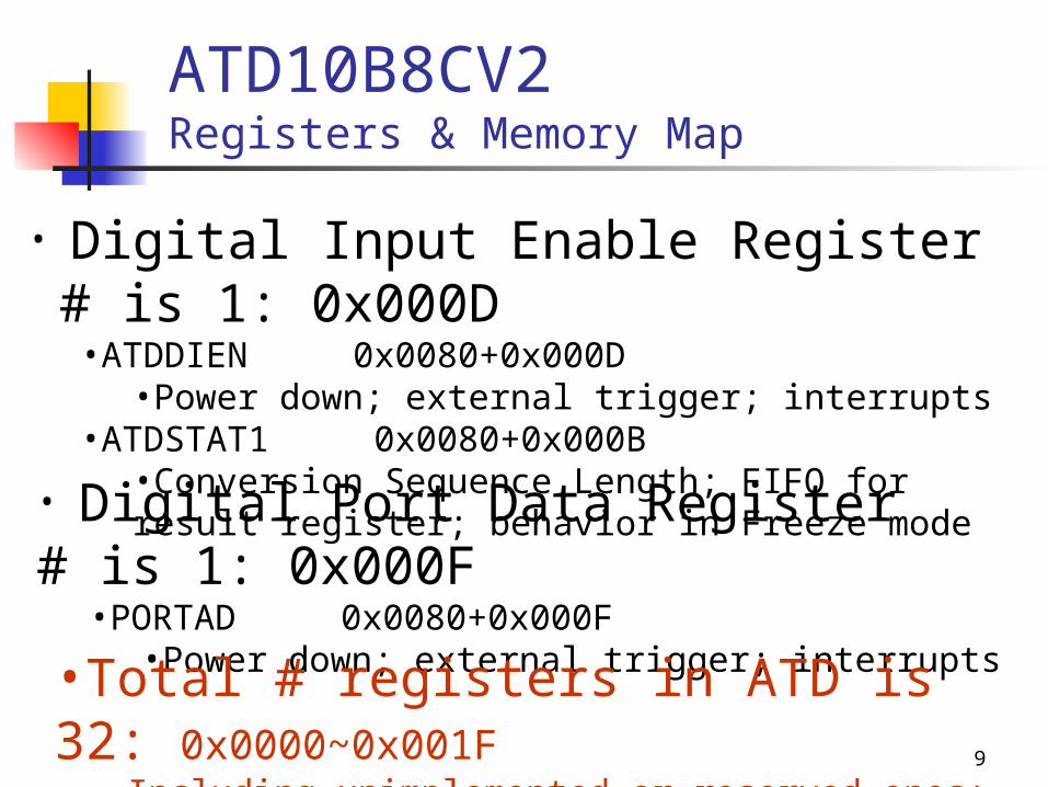
ATD10B8CV2Registers & Memory Map
• Digital Input Enable Register # is 1: 0x000D•ATDDIEN 0x0080+0x000D
•Power down; external trigger; interrupts•ATDSTAT1 0x0080+0x000B
•Conversion Sequence Length; FIFO for result register; behavior in Freeze mode
• Digital Port Data Register # is 1: 0x000F•PORTAD 0x0080+0x000F
•Power down; external trigger; interrupts
•Total # registers in ATD is 32: 0x0000~0x001F•Including unimplemented or reserved ones:
10
ATD10B8CV2 - Control Registers
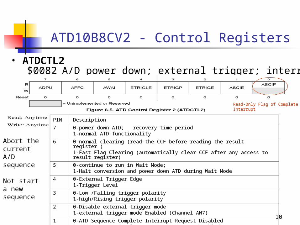
• ATDCTL2$0082 A/D power down; external trigger; interrupt
PIN Description
7 0-power down ATD; recovery time period1-normal ATD functionality
6 0-normal clearing (read the CCF before reading the result register )1-Fast Flag Clearing (automatically clear CCF after any access to result register)
5 0-continue to run in Wait Mode;1-Halt conversion and power down ATD during Wait Mode
4 0-External Trigger Edge1-Trigger Level
3 0-Low /Falling trigger polarity1-high/Rising trigger polarity
2 0-Disable external trigger mode1-external trigger mode Enabled (Channel AN7)
1 0-ATD Sequence Complete Interrupt Request Disabled1-ATD Sequence Complete Interrupt Request Enabled
Abort the current A/Dsequence
Not start a new sequence
Read-Only Flag of Complete Interrupt

11
4-Conversion Sequence
Set MULT = 0 (for single channel) and SCAN = 0 (for consecutive)
Channel
ADR1then
Channel
ADR2then
Channel
ADR3then
Channel
ADR4Stop
CONSECUTIVE
Set MULT = 1 (for multiple channel) and SCAN = 1 (for continuous)
Ch
ADR1then
Ch+1
ADR2then
Ch+2
ADR3then
Ch+3
ADR4
Overwrite ADR’s
CONTINUOUS
12
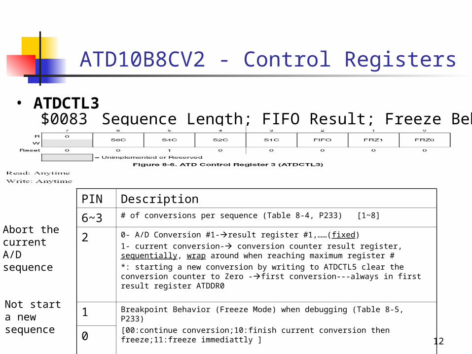
ATD10B8CV2 - Control Registers
• ATDCTL3$0083 Sequence Length; FIFO Result; Freeze Behavior
PIN Description
6~3 # of conversions per sequence (Table 8-4, P233) [1~8]
2 0- A/D Conversion #1-result register #1,……(fixed)
1- current conversion- conversion counter result register, sequentially, wrap around when reaching maximum register #
*: starting a new conversion by writing to ATDCTL5 clear the conversion counter to Zero -first conversion---always in first result register ATDDR0
1 Breakpoint Behavior (Freeze Mode) when debugging (Table 8-5, P233)
[00:continue conversion;10:finish current conversion then freeze;11:freeze immediattly ]
0
Abort the current A/Dsequence
Not start a new sequence
13
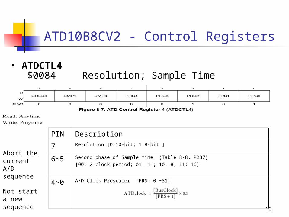
ATD10B8CV2 - Control Registers
• ATDCTL4$0084 Resolution; Sample Time
PIN Description
7 Resolution [0:10-bit; 1:8-bit ]
6~5 Second phase of Sample time (Table 8-8, P237)
[00: 2 clock period; 01: 4 ; 10: 8; 11: 16]
4~0 A/D Clock Prescaler [PRS: 0 ~31]
Abort the current A/Dsequence
Not start a new sequence
14
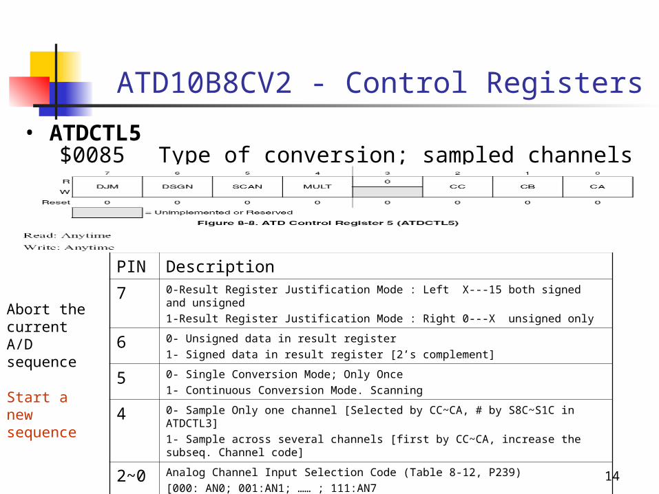
ATD10B8CV2 - Control Registers
• ATDCTL5$0085 Type of conversion; sampled channels
PIN Description
7 0-Result Register Justification Mode : Left X---15 both signed and unsigned
1-Result Register Justification Mode : Right 0---X unsigned only
6 0- Unsigned data in result register
1- Signed data in result register [2’s complement]
5 0- Single Conversion Mode; Only Once
1- Continuous Conversion Mode. Scanning
4 0- Sample Only one channel [Selected by CC~CA, # by S8C~S1C in ATDCTL3]
1- Sample across several channels [first by CC~CA, increase the subseq. Channel code]
2~0 Analog Channel Input Selection Code (Table 8-12, P239)
[000: AN0; 001:AN1; …… ; 111:AN7
MULT=0: selected channel;
MULT=1: first channel in sequence, then sequentially, auto-wrap]
Abort the current A/Dsequence
Start a new sequence
15
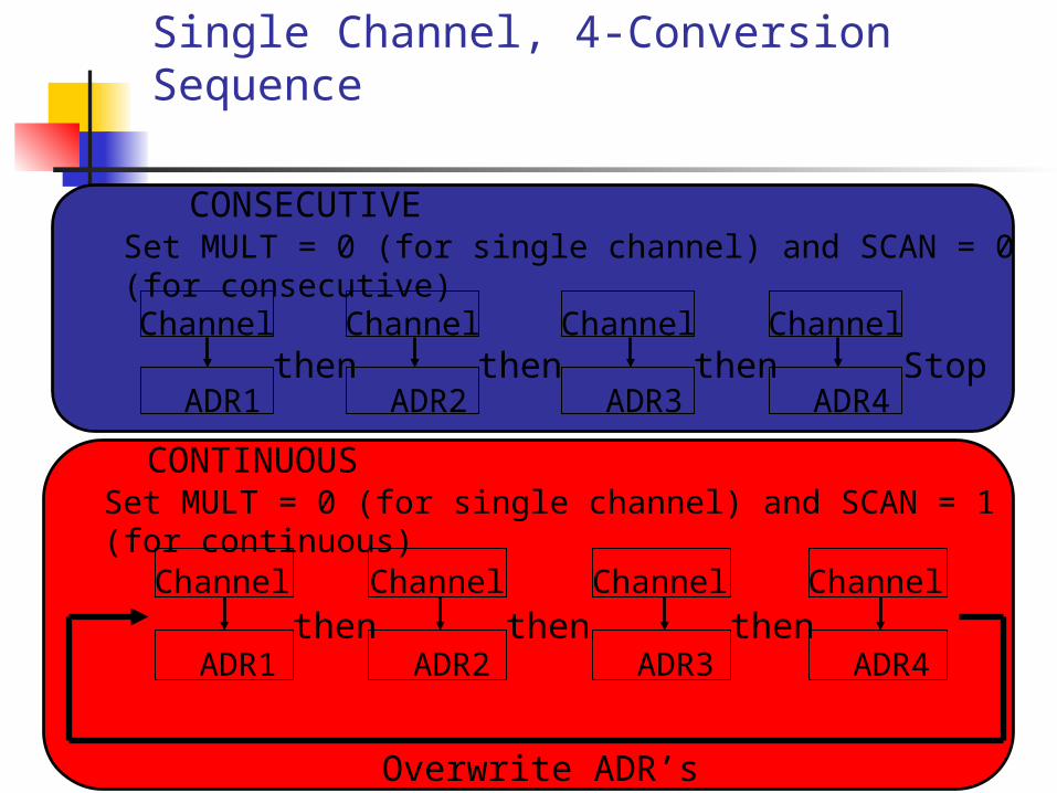
Single Channel, 4-Conversion Sequence
Set MULT = 0 (for single channel) and SCAN = 0 (for consecutive)
Channel
ADR1then
Channel
ADR2then
Channel
ADR3then
Channel
ADR4Stop
Set MULT = 0 (for single channel) and SCAN = 1 (for continuous)
Channel
ADR1then
Channel
ADR2then
Channel
ADR3then
Channel
ADR4
Overwrite ADR’s
CONSECUTIVE
CONTINUOUS
16
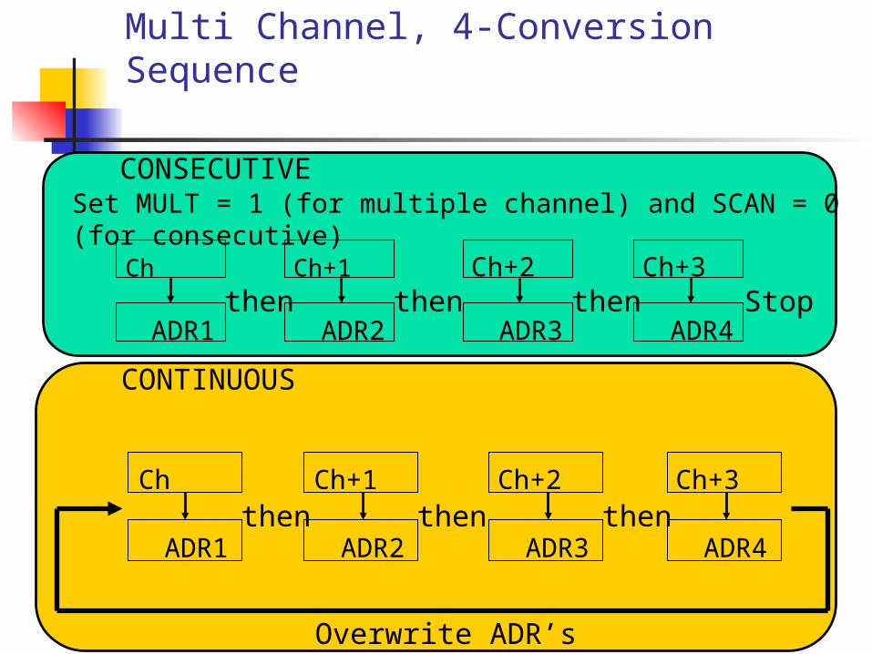
Multi Channel, 4-Conversion Sequence
Set MULT = 1 (for multiple channel) and SCAN = 0 (for consecutive)
Ch
ADR1then
Ch+1
ADR2then
Ch+2
ADR3then
Ch+3
ADR4Stop
Set MULT = 1 (for multiple channel) and SCAN = 1 (for continuous)
CONSECUTIVE
Ch
ADR1then
Ch+1
ADR2then
Ch+2
ADR3then
Ch+3
ADR4
Overwrite ADR’s
CONTINUOUS
17
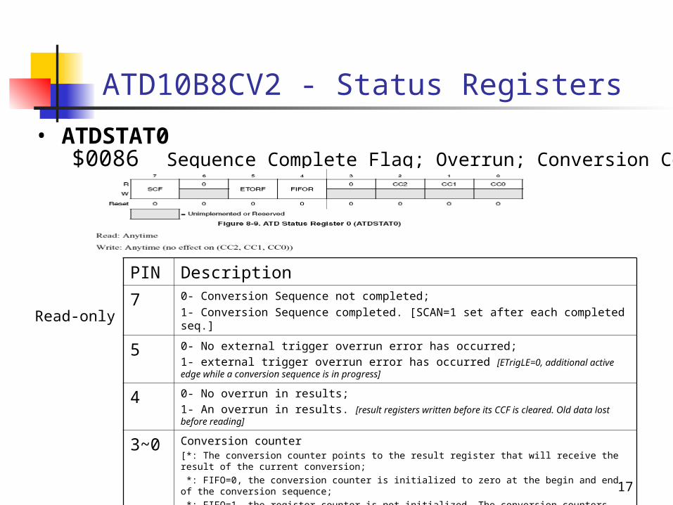
ATD10B8CV2 - Status Registers
• ATDSTAT0$0086 Sequence Complete Flag; Overrun; Conversion Counter
PIN Description
7 0- Conversion Sequence not completed;
1- Conversion Sequence completed. [SCAN=1 set after each completed seq.]
5 0- No external trigger overrun error has occurred;
1- external trigger overrun error has occurred [ETrigLE=0, additional active edge while a conversion sequence is in progress]
4 0- No overrun in results;
1- An overrun in results. [result registers written before its CCF is cleared. Old data lost before reading]
3~0 Conversion counter[*: The conversion counter points to the result register that will receive the result of the current conversion;
*: FIFO=0, the conversion counter is initialized to zero at the begin and end of the conversion sequence;
*: FIFO=1, the register counter is not initialized. The conversion counters wraps
around when its maximum value is reached.]
Read-only
18
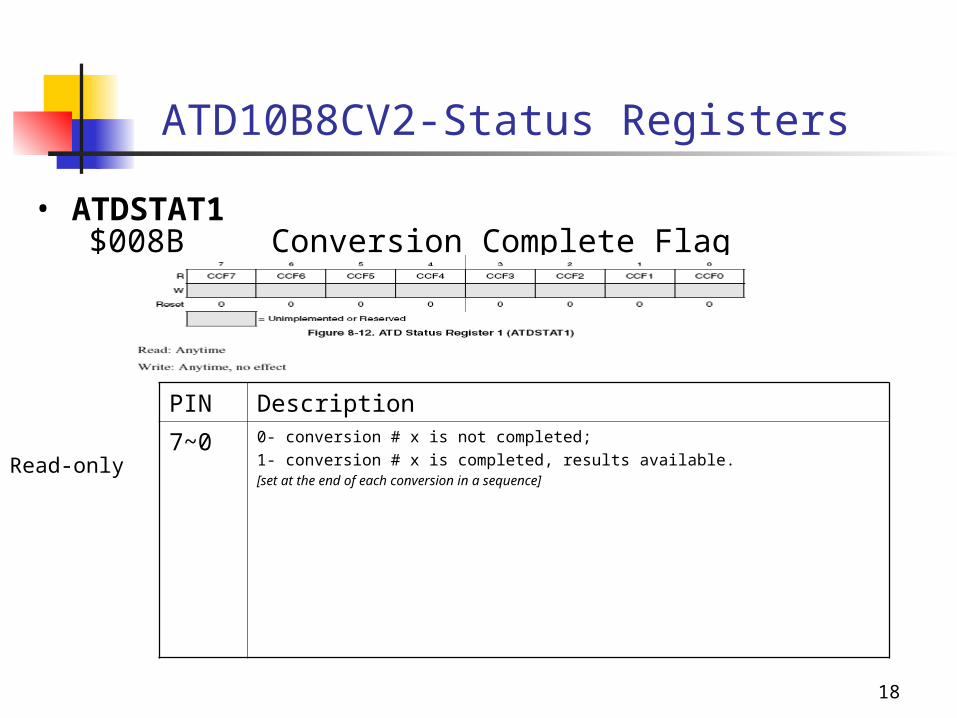
ATD10B8CV2-Status Registers
• ATDSTAT1$008B Conversion Complete Flag
PIN Description
7~0 0- conversion # x is not completed;
1- conversion # x is completed, results available.[set at the end of each conversion in a sequence]
Read-only
19
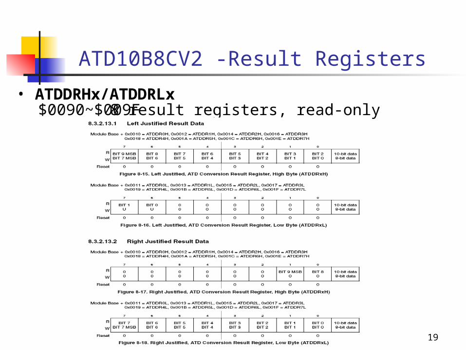
ATD10B8CV2 -Result Registers
• ATDDRHx/ATDDRLx$0090~$009F 8 result registers, read-only
20
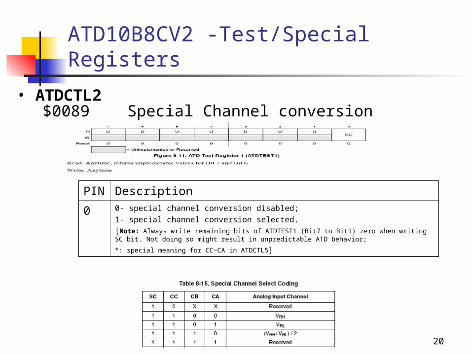
ATD10B8CV2 -Test/Special Registers
• ATDCTL2$0089 Special Channel conversion
PIN Description
0 0- special channel conversion disabled;
1- special channel conversion selected.
[Note: Always write remaining bits of ATDTEST1 (Bit7 to Bit1) zero when writing SC bit. Not doing so might result in unpredictable ATD behavior;
*: special meaning for CC~CA in ATDCTL5]
21
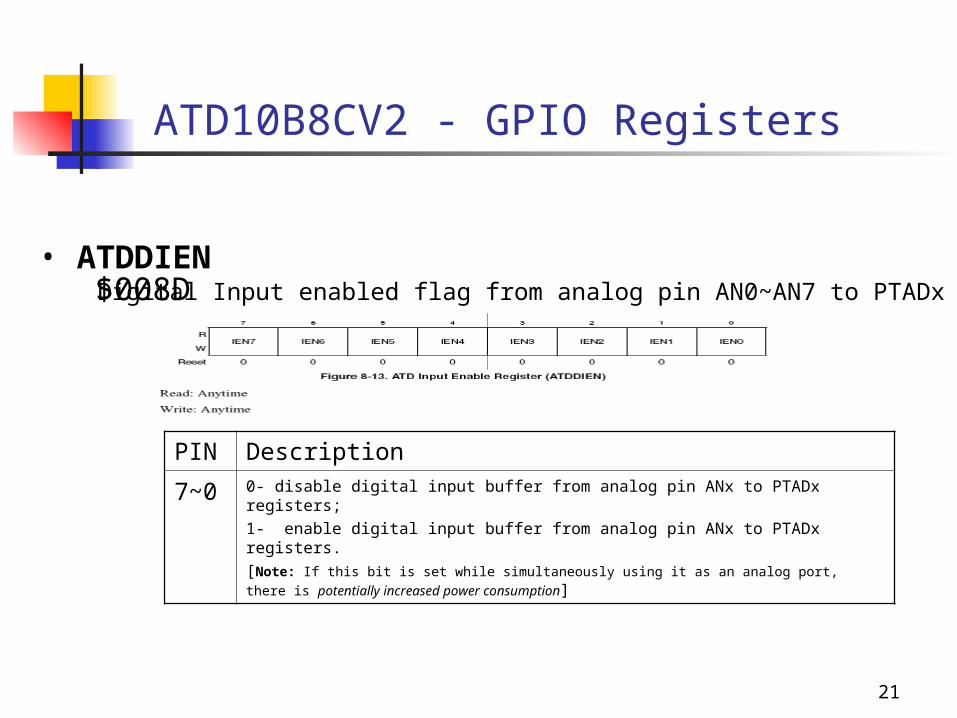
ATD10B8CV2 - GPIO Registers
• ATDDIEN$008D Digital Input enabled flag from analog pin AN0~AN7 to PTADx registers
PIN Description
7~0 0- disable digital input buffer from analog pin ANx to PTADx registers;
1- enable digital input buffer from analog pin ANx to PTADx registers.
[Note: If this bit is set while simultaneously using it as an analog port, there is potentially increased power
consumption]

22
ATD10B8CV2 - GPIO Registers
• PORTAD$008F GPIO port data registers
PIN Description
7~0 If IENx=1, Read the logic level on ANx pin
[Note: signal potentials not meeting VIL or VIH specifications will have an indeterminate value]
23
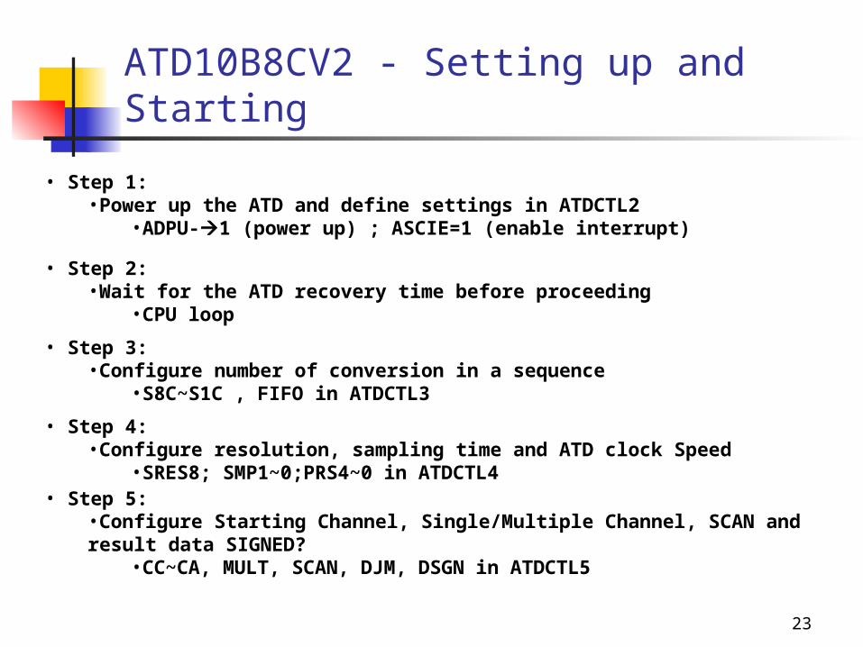
ATD10B8CV2 - Setting up and Starting
• Step 1: •Power up the ATD and define settings in ATDCTL2
•ADPU-1 (power up) ; ASCIE=1 (enable interrupt)
• Step 2: •Wait for the ATD recovery time before proceeding
•CPU loop
• Step 3: •Configure number of conversion in a sequence
•S8C~S1C , FIFO in ATDCTL3
• Step 4: •Configure resolution, sampling time and ATD clock Speed
•SRES8; SMP1~0;PRS4~0 in ATDCTL4• Step 5:
•Configure Starting Channel, Single/Multiple Channel, SCAN and result data SIGNED? •CC~CA, MULT, SCAN, DJM, DSGN in ATDCTL5
24
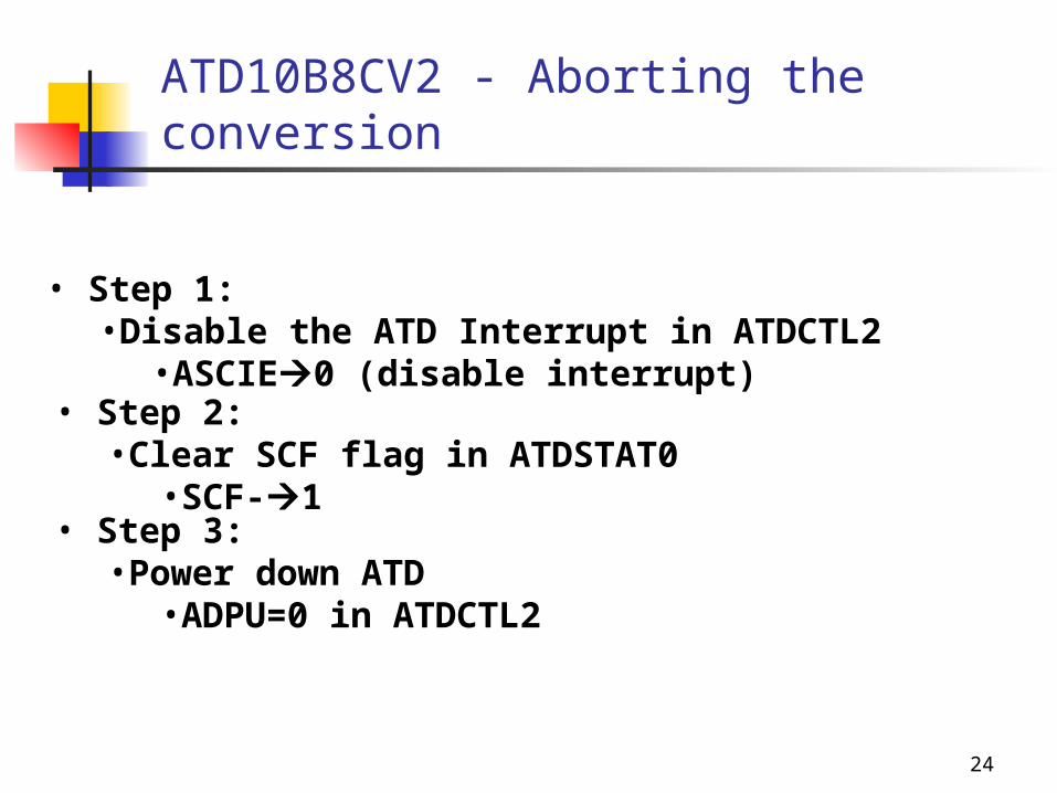
ATD10B8CV2 - Aborting the conversion
• Step 1: •Disable the ATD Interrupt in ATDCTL2
•ASCIE0 (disable interrupt)• Step 2:
•Clear SCF flag in ATDSTAT0•SCF-1
• Step 3: •Power down ATD
•ADPU=0 in ATDCTL2
25
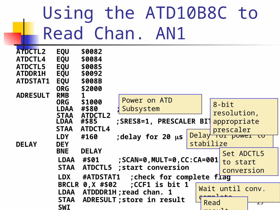
Using the ATD10B8C to Read Chan. AN1
ORG $1000 LDAA #$80 ;ADPU=1 STAA ATDCTL2
Power on ATD Subsystem
ATDCTL2 EQU $0082ATDCTL4 EQU $0084ATDCTL5 EQU $0085ATDDR1H EQU $0092ATDSTAT1 EQU $008B ORG $2000ADRESULT RMB 1
Delay for power to stabilize LDY #160 ;delay for 20 sDELAY DEY BNE DELAY LDAA #$01 ;SCAN=0,MULT=0,CC:CA=001 STAA ATDCTL5 ;start conversion LDX #ATDSTAT1 ;check for complete flag BRCLR 0,X #$02 ;CCF1 is bit 1 LDAA ATDDDR1H ;read chan. 1 STAA ADRESULT ;store in result
SWI
Set ADCTL5 to start conversion
Wait until conv. complete
Read result
LDAA #$85 ;SRES8=1, PRESCALER BITS = 00101 STAA ATDCTL4
8-bit resolution, appropriate prescaler
26
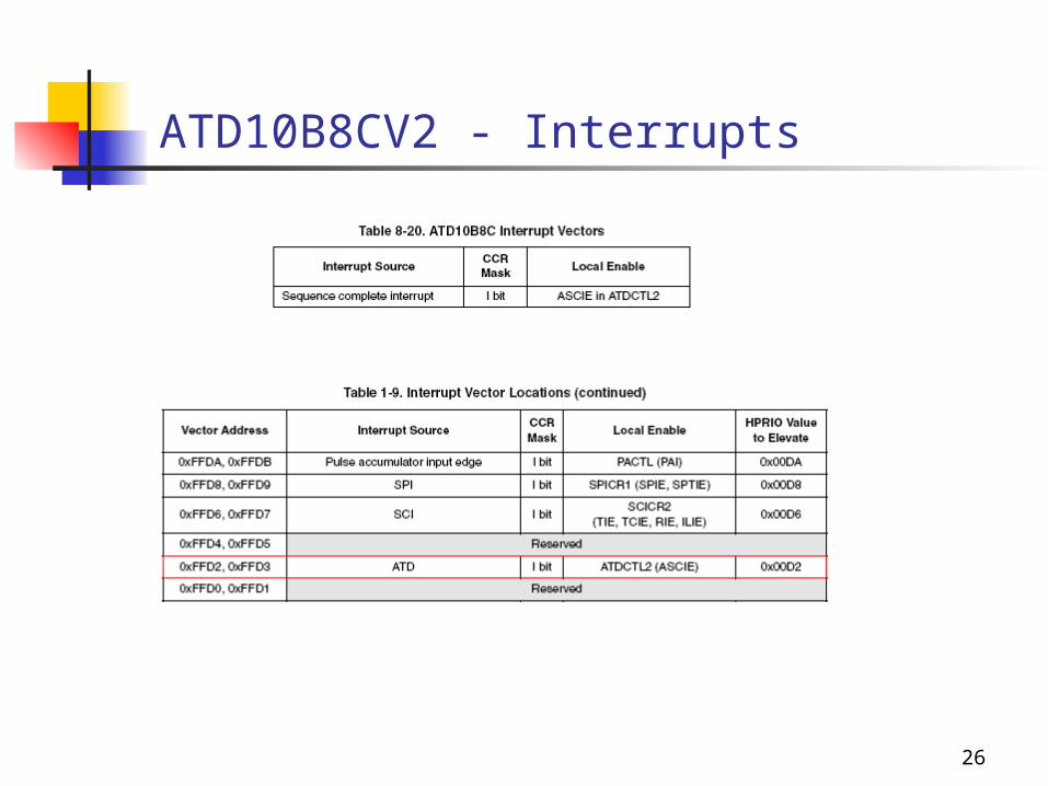
ATD10B8CV2 - Interrupts
27
A/D Conversion with the ATD10B8C
Chapter 8 in Reference Manual Pg. 223-249 in Reference Guide
Where to look:
28
References
Ron Bishop, “Basic Microprocessors and the 6800”, Hayden Book Company Inc., 1979
Motorola, “MC912SC Family Data Sheet”, Motorola, Inc., Rev. 5, 2007.
Motorola, “MC912SC Reference Manual”, Motorola, Inc., Rev. 4, 2007.
Motorola, “MC912SC Programming Reference Guide”, Motorola, Inc., Rev. 2, 2007.
Wikipedia The book
http://www.me.gatech.edu/mechatronics_course/