Embed Size (px)
Citation preview
1
Chapter 4 Modulation and Demodulation
Modulation/Demodulation schemes, Receiver design,
Signal-to-noise ratio (SNR), Bit error rate (BER)
2
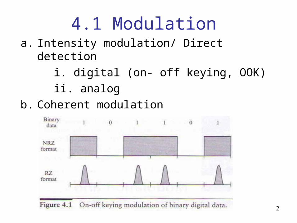
4.1 Modulation a. Intensity modulation/ Direct detection
i. digital (on- off keying, OOK)
ii. analog
b. Coherent modulation
3
4.1.1 Signal format (digital)
a. Unipolar return-to-zero (RZ, x%)b. Unipolar non-return-to-zero (NRE)i. need good DC balanceii. For time recover circuits, transitions are
needed. (line coding or scrambling) [(8,10) or (4,5) coding needs extra bandwidth]
The NRE format is very popular for high speed communication systems (e.g. 10Gb/s)
4
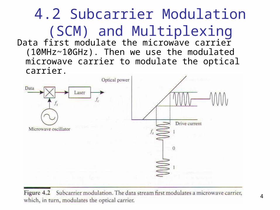
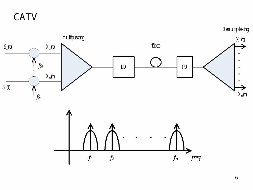
4.2 Subcarrier Modulation (SCM) and Multiplexing
Data first modulate the microwave carrier (10MHz~10GHz). Then we use the modulated microwave carrier to modulate the optical carrier.
5
6
CATV
S1(t) X1(t)
Sn(t)
fs1
fsn
Xn(t)
multiplexing
LD PD
X1(t)
Xn(t)
Demultiplexing
fiber
f1 f2 fn freq
7
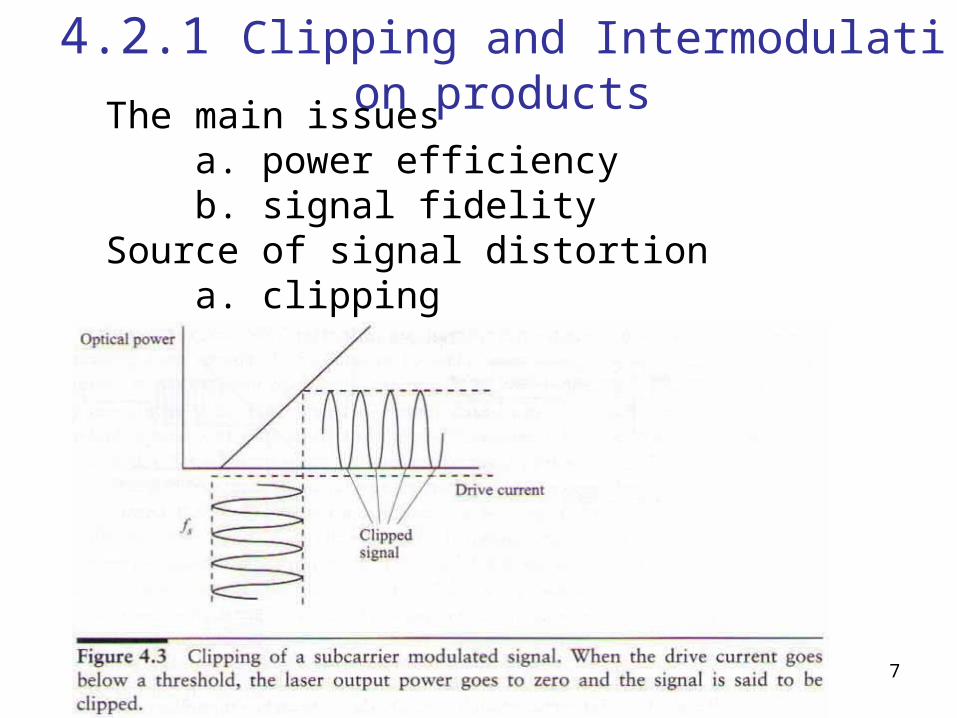
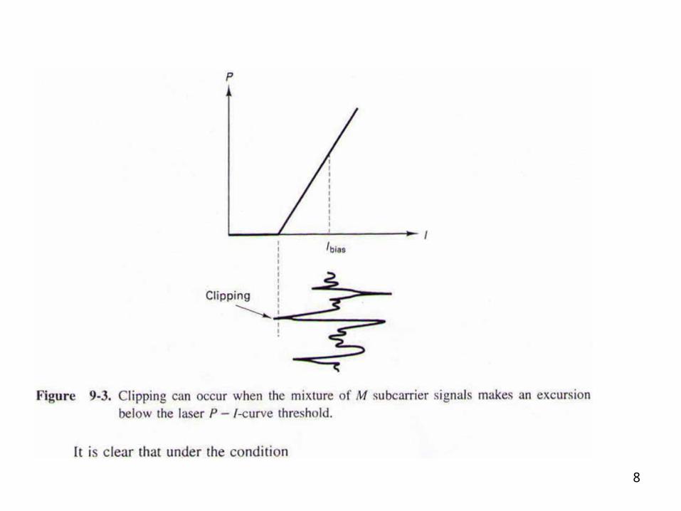
4.2.1 Clipping and Intermodulation productsThe main issues a. power efficiency b. signal fidelitySource of signal distortion a. clipping
8
9
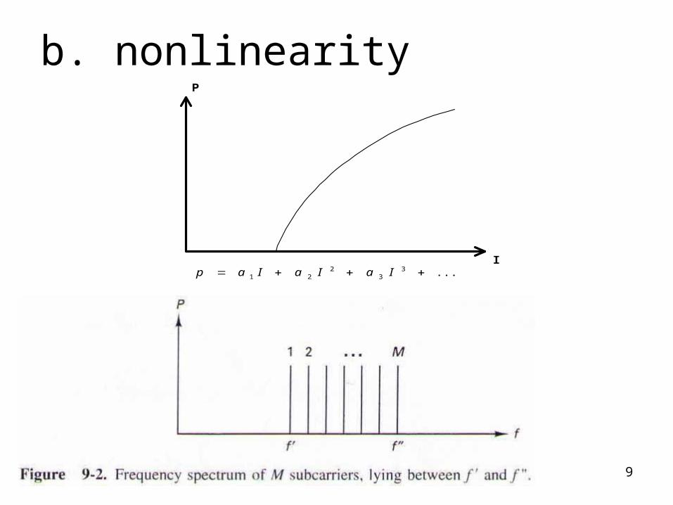
b. nonlinearityP
I2 3
1 2 3 . . .p a I a I a I
10
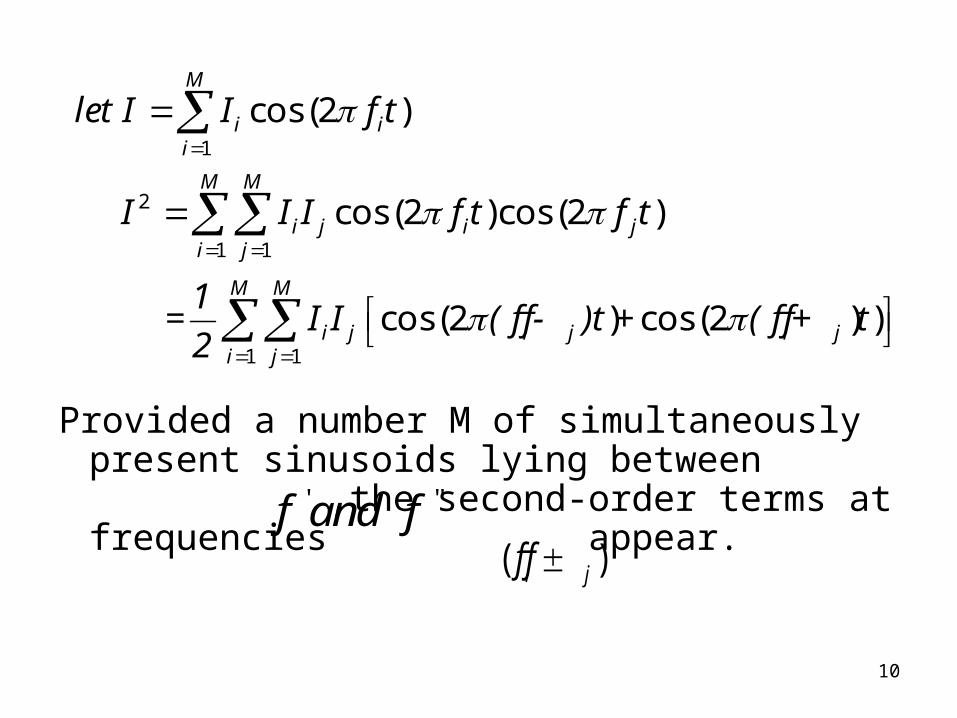
Provided a number M of simultaneously present sinusoids lying between ,the second-order terms at frequencies appear.
1 = ( - ) + ( +
2
1
2
1 1
1 1
cos(2 )
cos(2 )cos(2 )
cos(2 ) cos(2 ) )
M
i ii
M M
i j i ji j
M M
i j i j i ji j
let I I f t
I I I f t f t
I I f f t f f t
' ''f and f( )i jf f
11
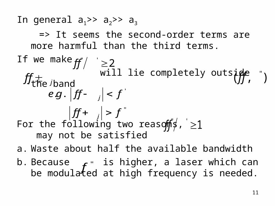
In general a1>> a2>> a3
=> It seems the second-order terms are more harmful than the third terms.
If we make
will lie completely outside the band
For the following two reasons, may not be satisfied
a. Waste about half the available bandwidth
b. Because is higher, a laser which can be modulated at high frequency is needed.
'' ' 2f f
i jf f ' ''( , )f f'
''
. . i j
i j
e g f f f
f f f
'' ' 1f f
''f
12
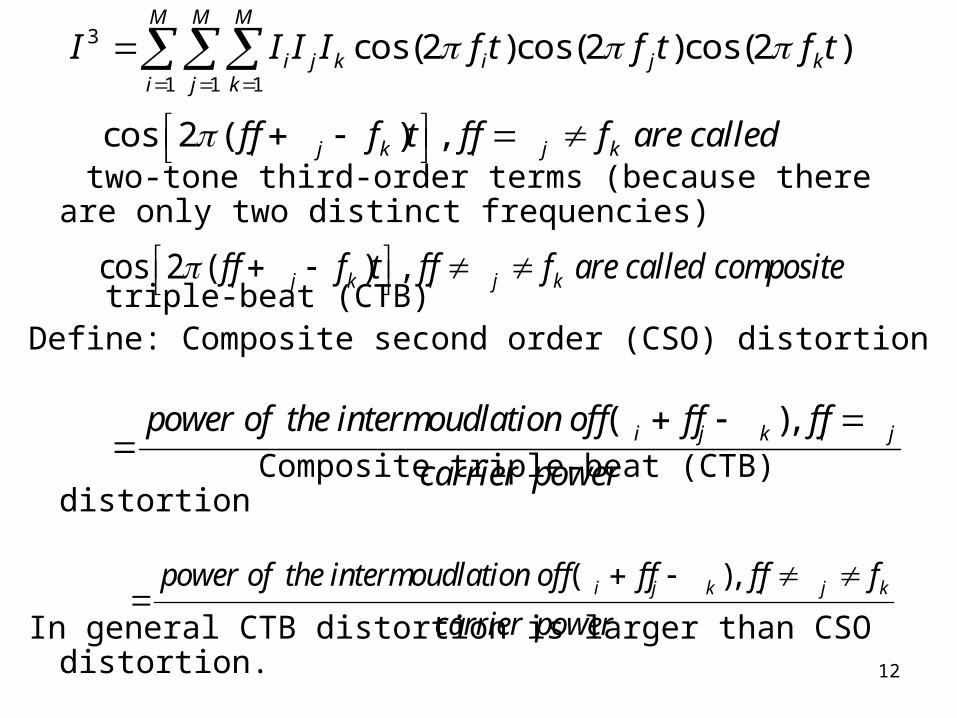
two-tone third-order terms (because there are only two distinct frequencies)
triple-beat (CTB)Define: Composite second order (CSO) distortion
Composite triple-beat (CTB) distortion
In general CTB distortion is larger than CSO distortion.
3
1 1 1
cos(2 )cos(2 )cos(2 )
cos 2 ( ) ,
M M M
i j k i j ki j k
i j k i j k
I I I I f t f t f t
f f f t f f f are called
cos 2 ( ) ,i j k i j kf f f t f f f are called composite
( ),i j k i jpower of the intermoudlation of f f f f f
carrier power
( ),i j k i j kpower of the intermoudlation of f f f f f f
carrier power
13
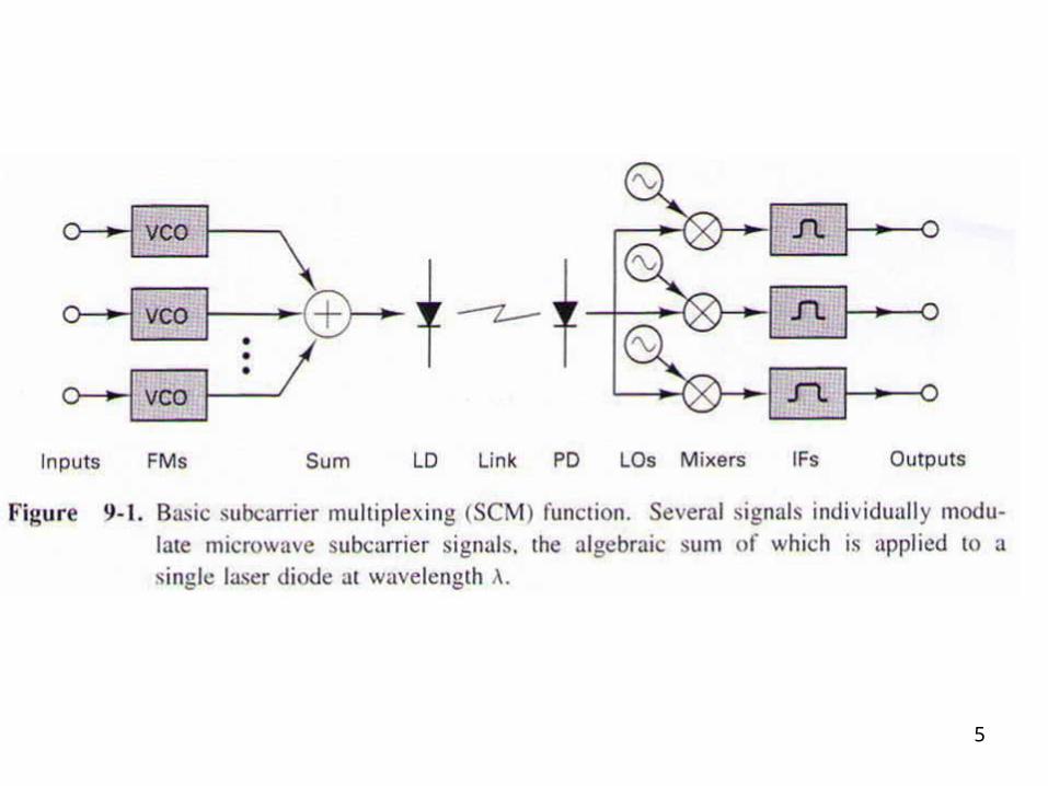
4.2.2 Applications of SCM
a. Transmitting multiple analog video signal using a single optical transmitter. (CATV, Hybrid fiber-coax HFC)
b. Carrying control data along with the actual data steam. For example, the pilot tone in WDM systems.
14
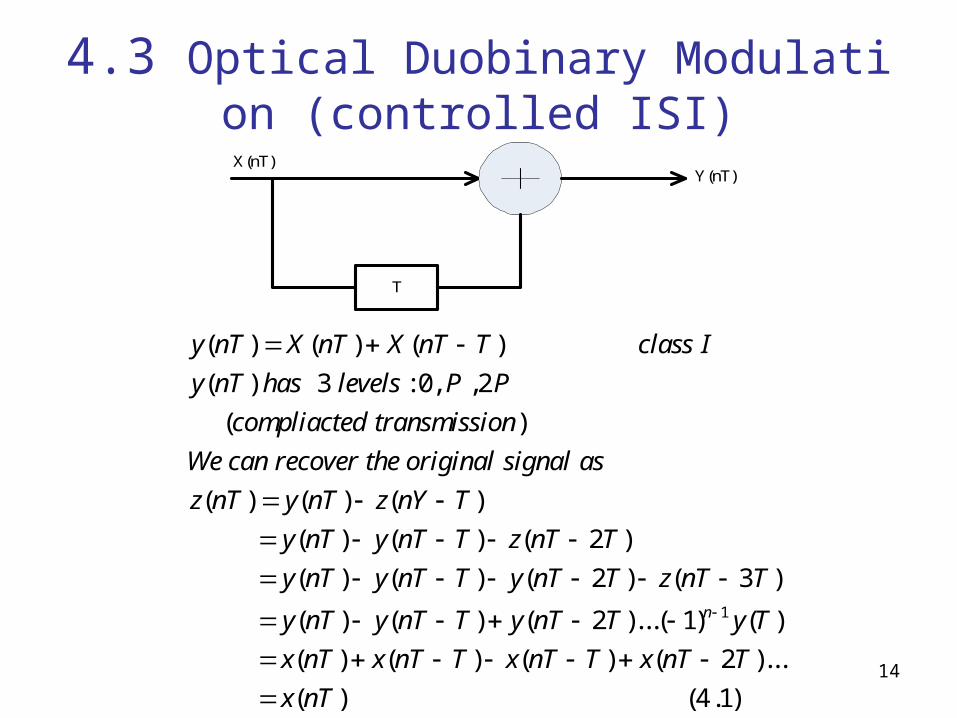
4.3 Optical Duobinary Modulation (controlled ISI)
T
X(nT)Y(nT)
( ) ( ) ( )
( ) 3 : 0, ,2
( )
( ) ( ) ( )
( ) ( ) ( 2 )
( ) ( ) ( 2 ) ( 3 )
( ) ( ) ( 2 )
y nT X nT X nT T class I
y nT has levels P P
compliacted transmission
We can recover the original signal as
z nT y nT z nY T
y nT y nT T z nT T
y nT y nT T y nT T z nT T
y nT y nT T y nT T
1...( 1) ( )
( ) ( ) ( ) ( 2 )...
( ) (4.1)
n y T
x nT x nT T x nT T x nT T
x nT
15
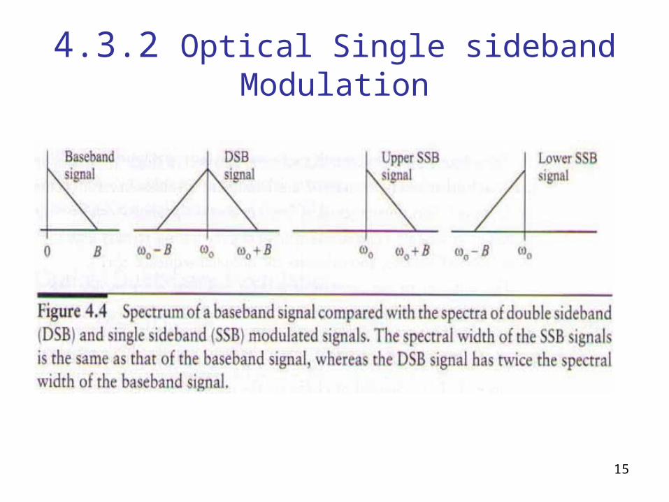
4.3.2 Optical Single sideband Modulation
16
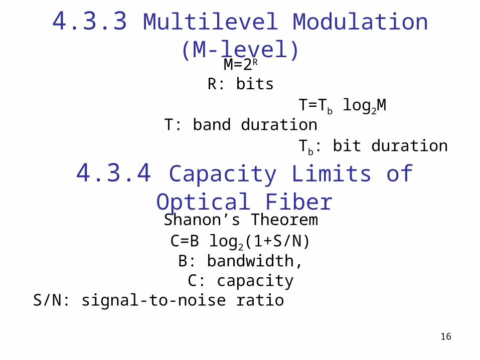
4.3.3 Multilevel Modulation (M-level)M=2R
R: bits T=Tb log2M
T: band duration Tb: bit duration
4.3.4 Capacity Limits of Optical Fiber
Shanon’s TheoremC=B log2(1+S/N)
B: bandwidth,C: capacity
S/N: signal-to-noise ratio
17
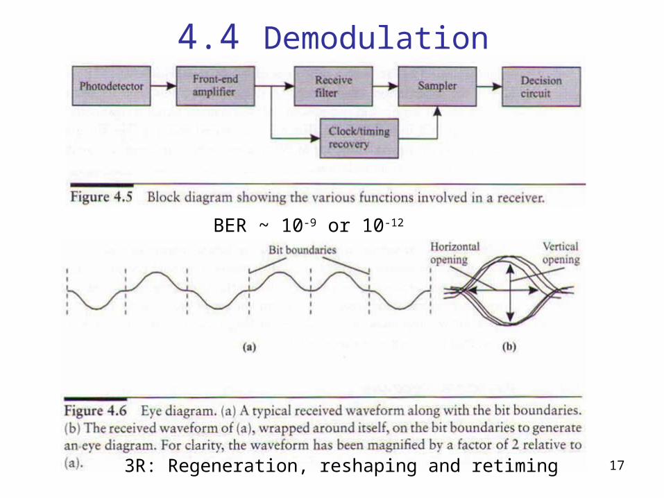
4.4 Demodulation
BER ~ 10-9 or 10-12
3R: Regeneration, reshaping and retiming
18
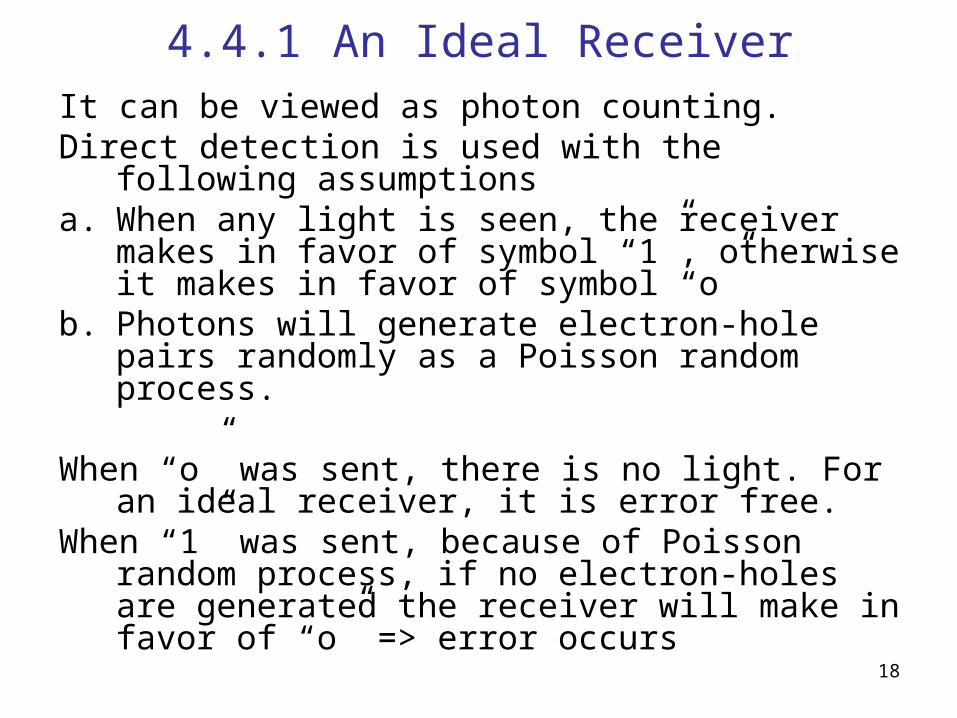
4.4.1 An Ideal Receiver
It can be viewed as photon counting.Direct detection is used with the following
assumptionsa. When any light is seen, the receiver makes in
favor of symbol “1”, otherwise it makes in favor of symbol “o”
b. Photons will generate electron-hole pairs randomly as a Poisson random process.
When “o” was sent, there is no light. For an ideal receiver, it is error free.
When “1” was sent, because of Poisson random process, if no electron-holes are generated the receiver will make in favor of “o” => error occurs
19
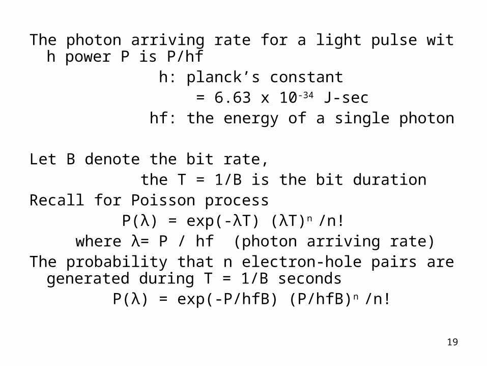
The photon arriving rate for a light pulse with power P is P/hf
h: planck’s constant = 6.63 x 10⁻³⁴ J-sec hf: the energy of a single photon
Let B denote the bit rate, the T = 1/B is the bit durationRecall for Poisson process P(λ) = exp(-λT) (λT)n /n! where λ= P / hf (photon arriving rate)The probability that n electron-hole pairs are generated duri
ng T = 1/B seconds P(λ) = exp(-P/hfB) (P/hfB)n /n!
20
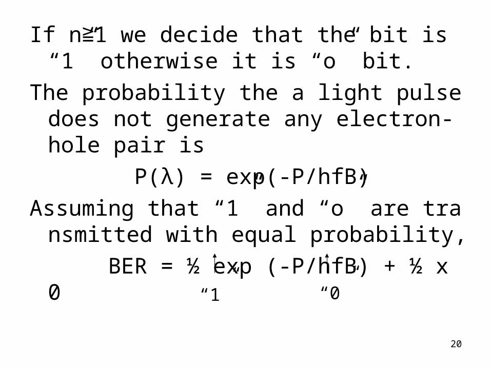
If n 1 we decide that the bit is “1” otherwise ≧it is “o” bit.
The probability the a light pulse does not generate any electron-hole pair is
P(λ) = exp(-P/hfB)
Assuming that “1” and “o” are transmitted with equal probability,
BER = ½ exp (-P/hfB) + ½ x 0
“1” “0”
21
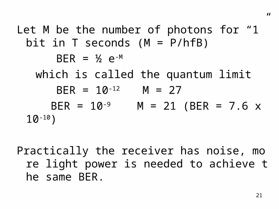
Let M be the number of photons for “1” bit in T seconds (M = P/hfB)
BER = ½ e-M
which is called the quantum limit
BER = 10-12 M = 27 BER = 10-9 M = 21 (BER = 7.6 x 10⁻¹⁰)
Practically the receiver has noise, more light power is needed to achieve the same BER.
22
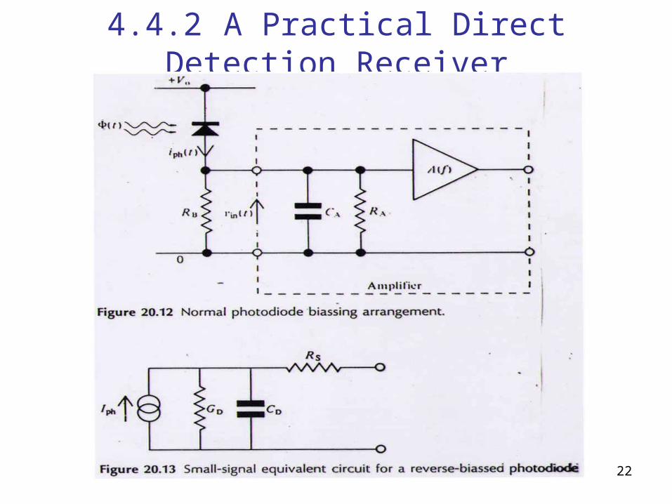
4.4.2 A Practical Direct Detection Receiver
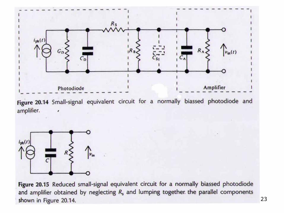
23
24
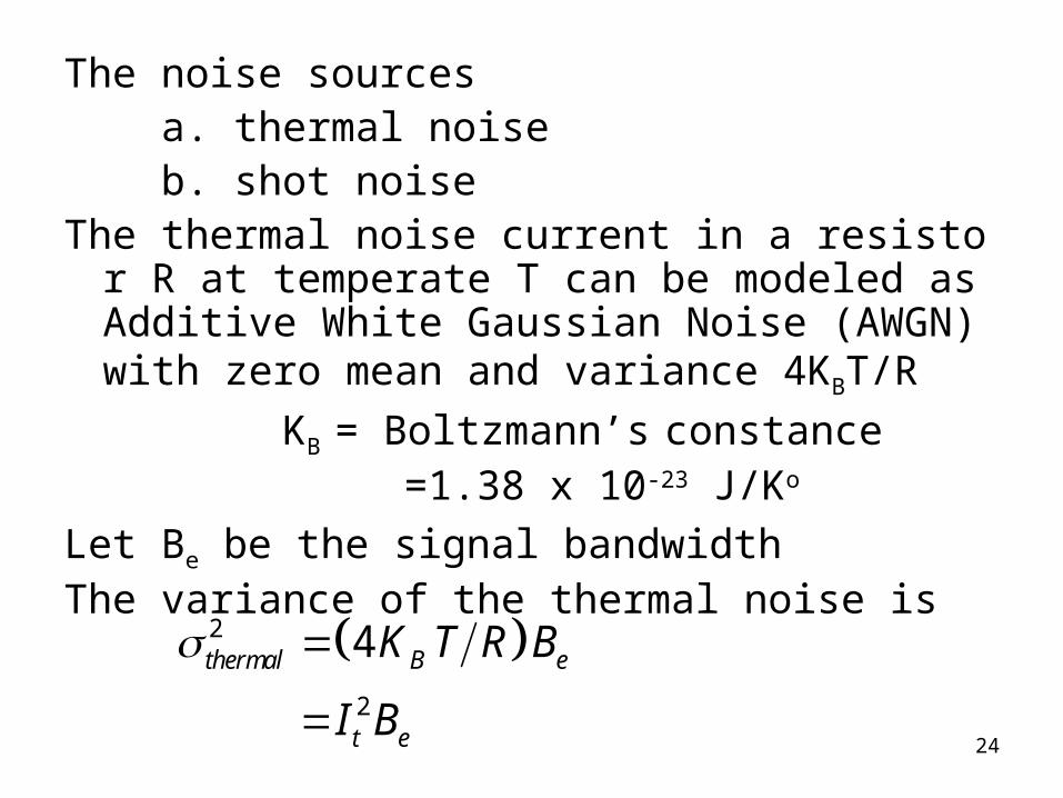
The noise sources a. thermal noise b. shot noiseThe thermal noise current in a resistor R at temper
ate T can be modeled as Additive White Gaussian Noise (AWGN) with zero mean and variance 4KBT/R
KB = Boltzmann’s constance =1.38 x 10⁻²³ J/Ko
Let Be be the signal bandwidth The variance of the thermal noise is 2
2
4thermal B e
t e
K T R B
I B
25
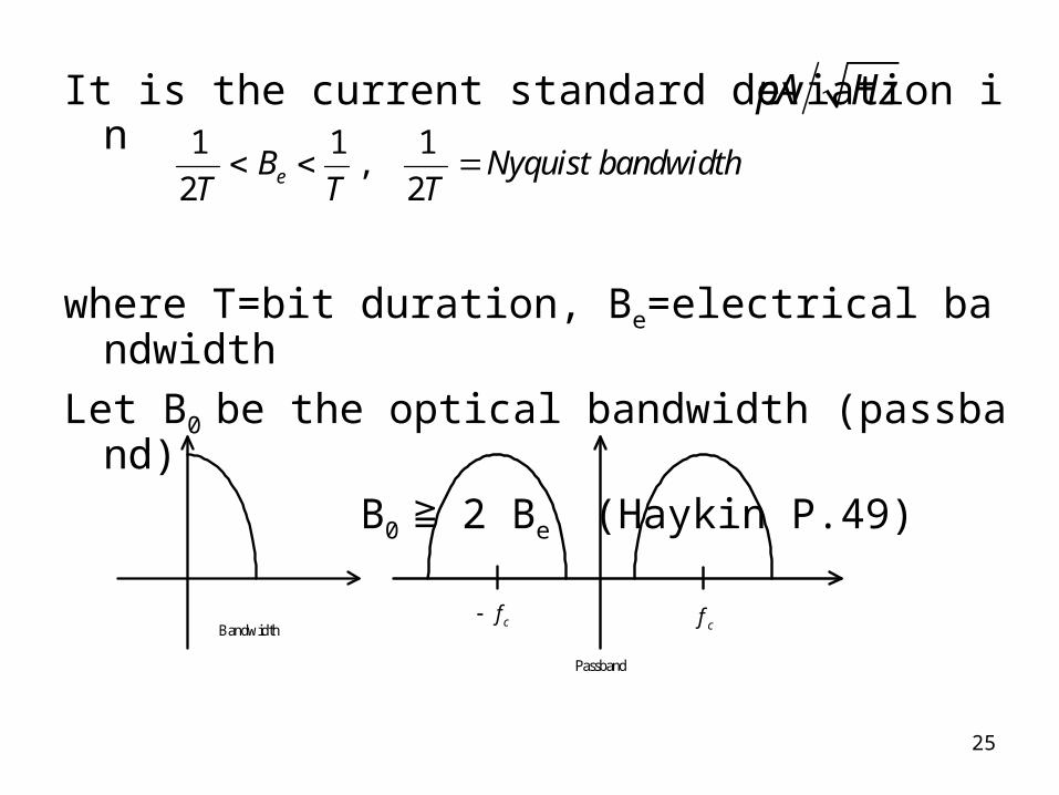
It is the current standard deviation in
where T=bit duration, Be=electrical bandwidth
Let B0 be the optical bandwidth (passband)
B0 2 B≧ e (Haykin P.49)
pA Hz1 1 1
,2 2eB Nyquist bandwidthT T T
Bandwidth
Passband
cf cf
26
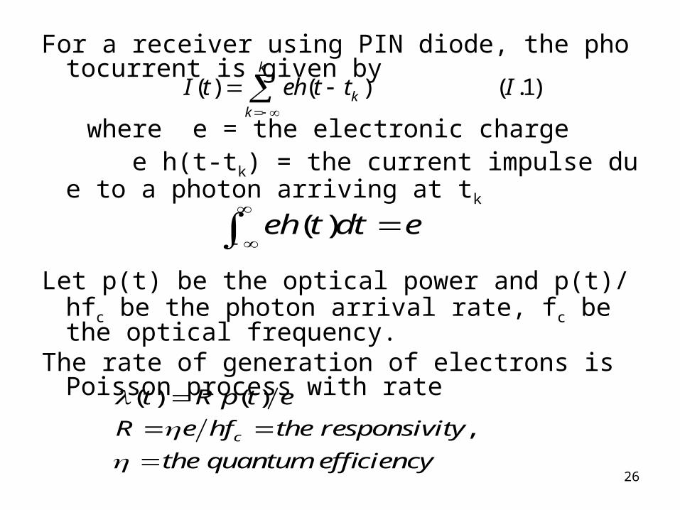
For a receiver using PIN diode, the photocurrent is given by
where e = the electronic charge e h(t-tk) = the current impulse due to a photon a
rriving at tk
Let p(t) be the optical power and p(t)/hfc be the photon arrival rate, fc be the optical frequency.
The rate of generation of electrons is Poisson process with rate
( ) ( ) ( .1)k
kk
I t eh t t I
( )eh t dt e
( ) ( )
,c
t R p t e
R e hf the responsivity
the quantum efficiency
27
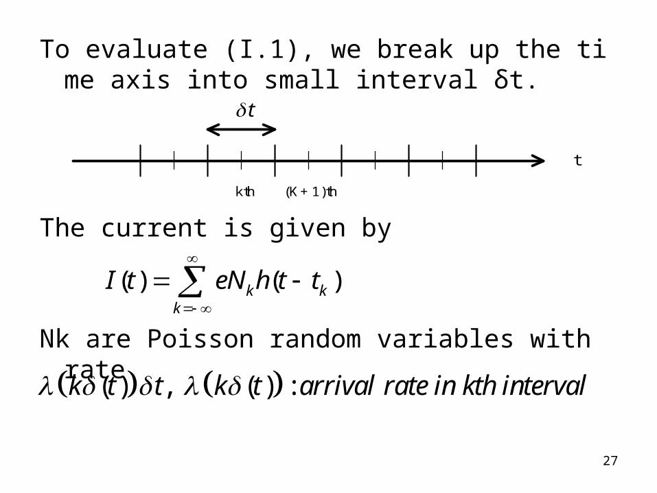
To evaluate (I.1), we break up the time axis into small interval δt.
The current is given by
Nk are Poisson random variables with rate
( ) ( )k kk
I t eN h t t
( ) , ( ) :k t t k t arrival rate in kth interval
t
t
kth (K+1)th
28
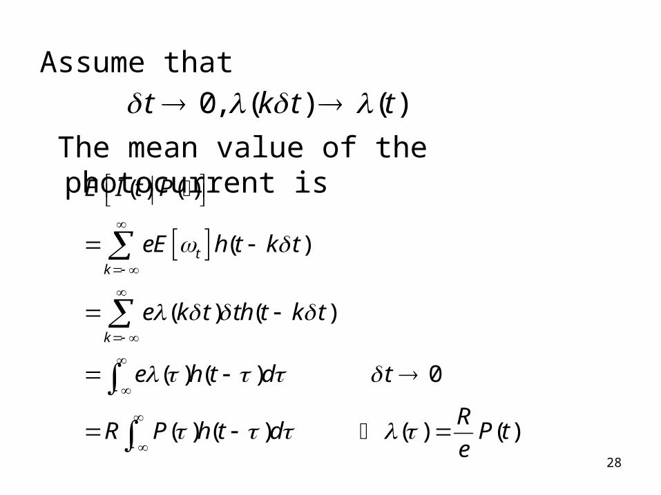
Assume that
The mean value of the photocurrent is
0, ( ) ( )t k t t
( ) ( )
( )
( ) ( )
( ) ( ) 0
( ) ( ) ( ) ( )
tk
k
E I t P
eE h t k t
e k t th t k t
e h t d t
RR P h t d P t
e
29
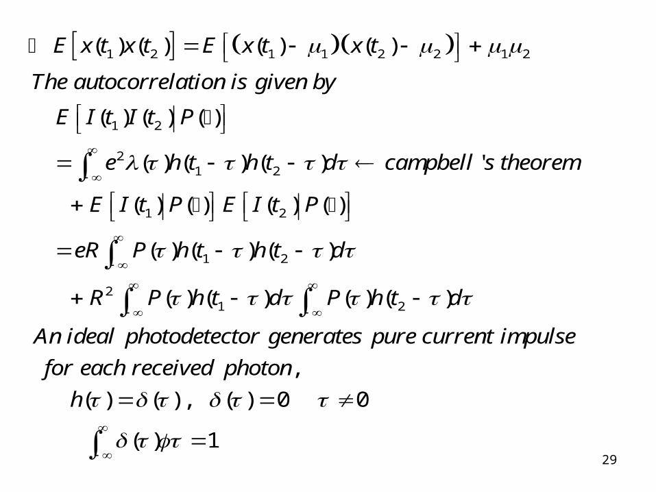
1 2 1 1 2 2 1 2
1 2
21 2
1 2
1 2
21
( ) ( ) ( ) ( )
( ) ( ) ( )
( ) ( ) ( ) '
( ) ( ) ( ) ( )
( ) ( ) ( )
( ) ( )
E x t x t E x t x t
The autocorrelation is given by
E I t I t P
e h t h t d campbell s theorem
E I t P E I t P
eR P h t h t d
R P h t
2( ) ( )
,
( ) ( ) , ( ) 0 0
( ) 1
d P h t d
An ideal photodetector generates pure current impulse
for each received photon
h
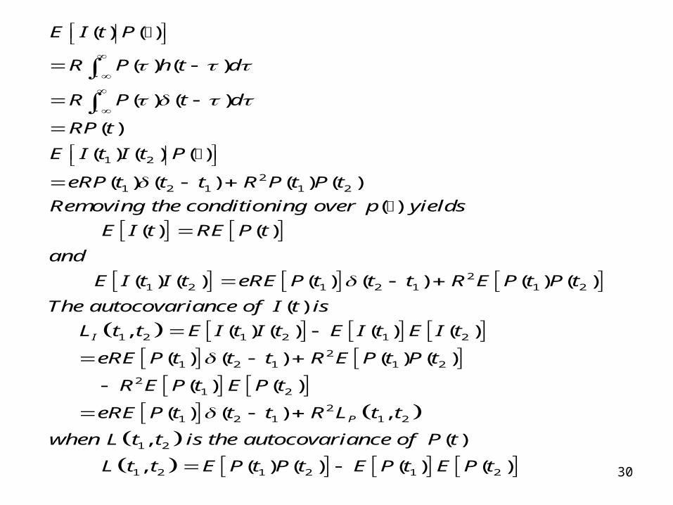
30
1 2
21 2 1 1 2
21 2 1 2 1 1 2
( ) ( )
( ) ( )
( ) ( )
( )
( ) ( ) ( )
( ) ( ) ( ) ( )
( )
( ) ( )
( ) ( ) ( ) ( ) ( ) ( )
E I t P
R P h t d
R P t d
RP t
E I t I t P
eRP t t t R P t P t
Removing the conditioning over p yields
E I t RE P t
and
E I t I t eRE P t t t R E P t P t
The
1 2 1 2 1 2
21 2 1 1 2
21 2
21 2 1 1 2
1 2
1 2 1 2 1 2
( )
, ( ) ( ) ( ) ( )
( ) ( ) ( ) ( )
( ) ( )
( ) ( ) ,
, ( )
, ( ) ( ) ( ) ( )
I
P
autocovariance of I t is
L t t E I t I t E I t E I t
eRE P t t t R E P t P t
R E P t E P t
eRE P t t t R L t t
when L t t is the autocovariance of P t
L t t E P t P t E P t E P t
31
Shot noise
1 2 1 2
2 1
( )
( ) 0, ( ) ( ) ( ) ( )
( )
( ) ( ),
( ) ( )
( )
( ) ( )exp( 2 )
( )exp( 2 )
P
I
I
I I
consider the simple case
E P t P constant
L E P t P t E P t E P t
where t t
E I t RP
L eRP
L eRP
The power spectral density PSD is
S f L i f d
eRP i f d
eRP depends on power
PSP
eRP
-Be Be
f
2
:
( ) 2e
e
e
B
shot I eB
B receiver bandwidth
S f df eRPB
32
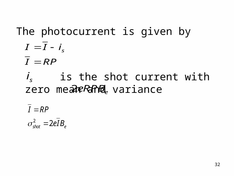
The photocurrent is given by
is the shot current with zero mean and variance
sI I i
I RP
si2 eeRPB
2 2shot e
I RP
eIB
33
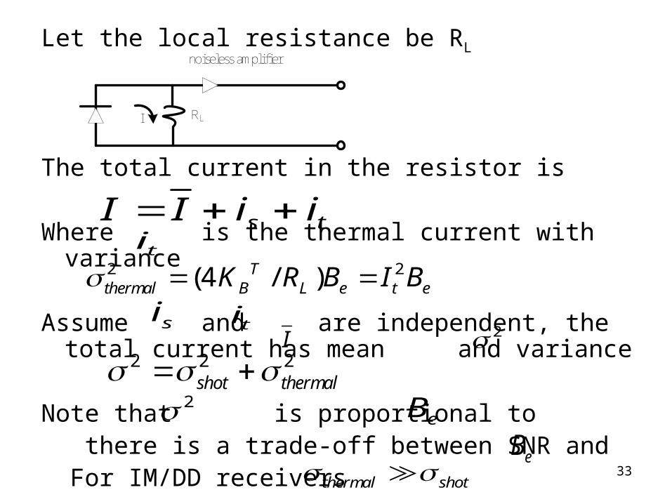
Let the local resistance be RL
The total current in the resistor is
Where is the thermal current with variance
Assume and are independent, the total current has mean and variance
Note that is proportional to there is a trade-off between SNR and For IM/DD receivers
noiseless amplifier
RLI
s tI I i i ti
2 2(4 / )Tthermal B L e t eK R B I B
tisiI 2
2 2 2shot thermal
2 eB
eBthermal shot
34
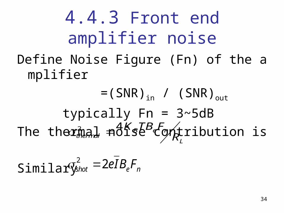
4.4.3 Front end amplifier noise
Define Noise Figure (Fn) of the amplifier
=(SNR)in / (SNR)out
typically Fn = 3~5dB
The thermal noise contribution is
Similary
2 4 B e nthermal
L
K TB FR
2 2shot e neIB F
35
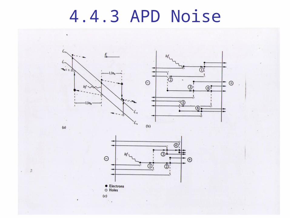
4.4.3 APD Noise
36
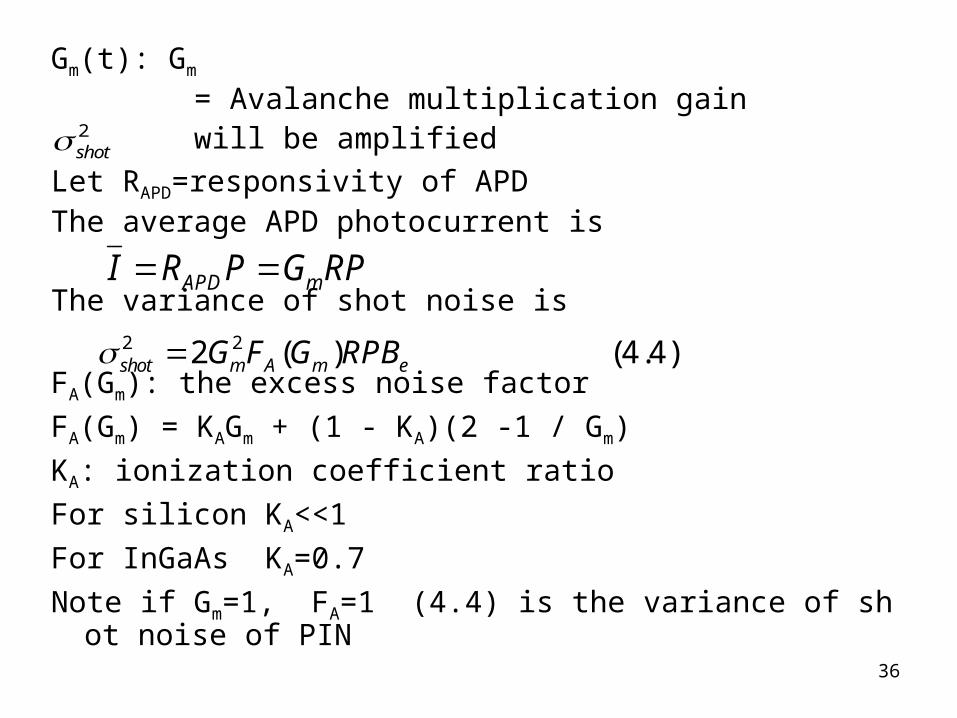
Gm(t): Gm
= Avalanche multiplication gain will be amplified
Let RAPD=responsivity of APDThe average APD photocurrent is
The variance of shot noise is
FA(Gm): the excess noise factor
FA(Gm) = KAGm + (1 - KA)(2 -1 / Gm)
KA: ionization coefficient ratio
For silicon KA<<1
For InGaAs KA=0.7
Note if Gm=1, FA=1 (4.4) is the variance of shot noise of PIN
2shot
APD mI R P G RP
2 22 ( ) (4.4)shot m A m eG F G RPB
37
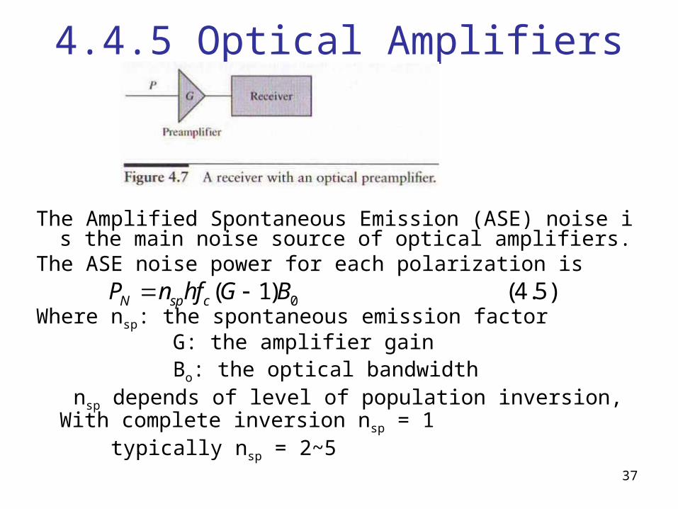
4.4.5 Optical Amplifiers
The Amplified Spontaneous Emission (ASE) noise is the main noise source of optical amplifiers.
The ASE noise power for each polarization is
Where nsp: the spontaneous emission factor G: the amplifier gain Bo: the optical bandwidth nsp depends of level of population inversion, With complet
e inversion nsp = 1 typically nsp = 2~5
0( 1) (4.5)N sp cP n hf G B
38
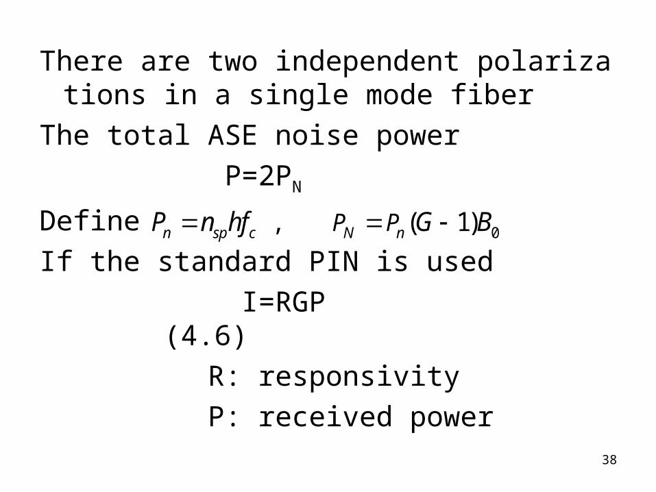
There are two independent polarizations in a single mode fiber
The total ASE noise power
P=2PN
Define
If the standard PIN is used
I=RGP (4.6)
R: responsivity
P: received power
0, ( 1)n sp c N nP PP n hf G B
39
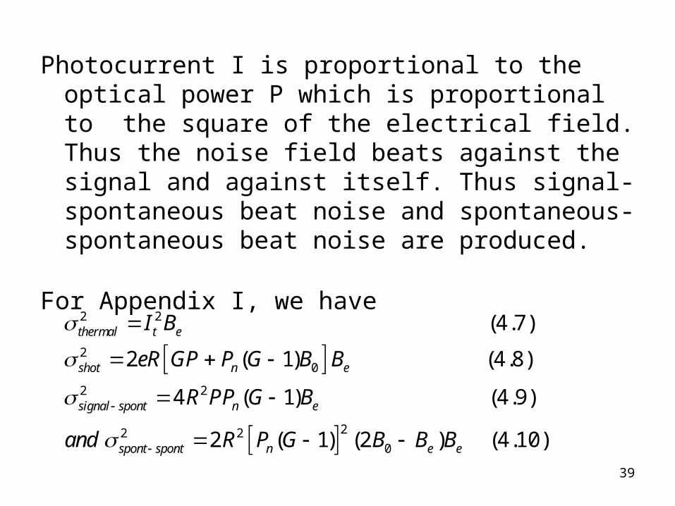
Photocurrent I is proportional to the optical power P which is proportional to the square of the electrical field. Thus the noise field beats against the signal and against itself. Thus signal-spontaneous beat noise and spontaneous-spontaneous beat noise are produced.
For Appendix I, we have
2 2
20
2 2
22 20
(4.7)
2 ( 1) (4.8)
4 ( 1) (4.9)
2 ( 1) (2 ) (4.10)
thermal t e
shot n e
signal spont n e
spont spont n e e
I B
eR GP P G B B
R PP G B
and R P G B B B
40
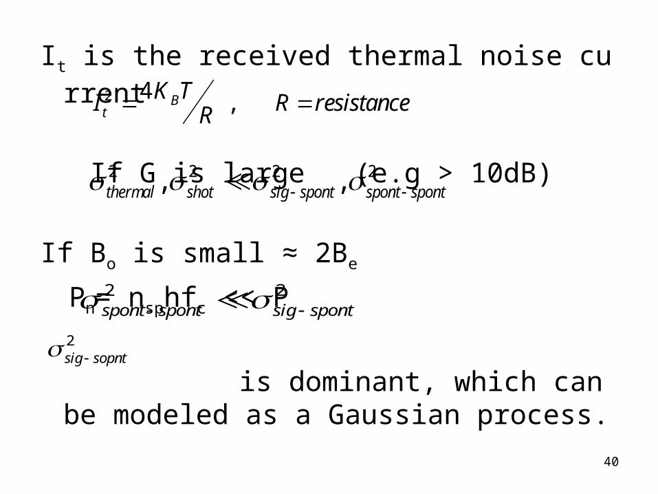
It is the received thermal noise current
If G is large (e.g > 10dB)
If Bo is small ≈ 2Be
Pn= nsphfc << P
is dominant, which can be modeled as a Gaussian process.
2 4 ,Bt
K TI R resistanceR
2 2 2 2, ,thermal shot sig spont spont spont
2 2spont spont sig spont
2sig sopnt
41
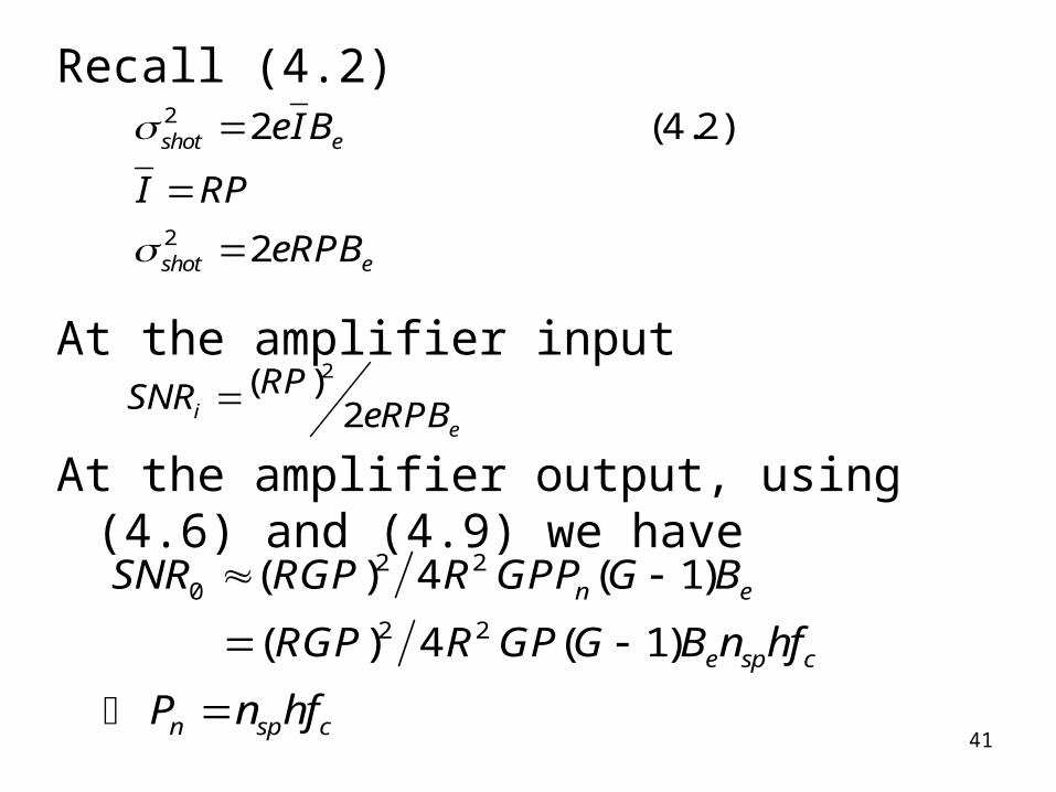
Recall (4.2)
At the amplifier input
At the amplifier output, using (4.6) and (4.9) we have
2
2
2 (4.2)
2
shot e
shot e
eIB
I RP
eRPB
2( )2i
e
RPSNR eRPB
2 20
2 2
( ) 4 ( 1)
( ) 4 ( 1)
n e
e sp c
n sp c
SNR RGP R GPP G B
RGP R GP G B n hf
P n hf
42
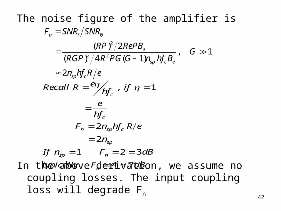
The noise figure of the amplifier is
In the above derivation, we assume no coupling losses. The input coupling loss will degrade Fn
0
2
2 2
( ) 2, 1
( ) 4 ( 1)
2
n i
e
sp c e
sp c
F SNR SNR
RP RePBG
RGP R PG G n hf B
n hf R e
, 1
2
2
1 2 3
4 ~ 7
c
c
n sp c
sp
sp n
n
eRecall R ifhf
e
hf
F n hf R e
n
If n F dB
typically F dB
43
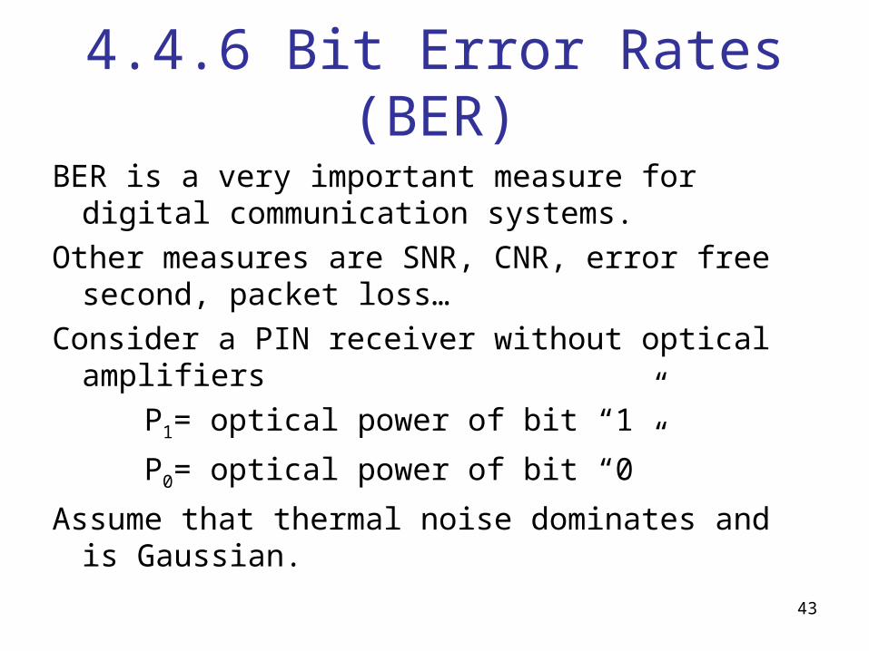
4.4.6 Bit Error Rates (BER)
BER is a very important measure for digital communication systems.
Other measures are SNR, CNR, error free second, packet loss…
Consider a PIN receiver without optical amplifiers
P1= optical power of bit “1”
P0= optical power of bit “0”
Assume that thermal noise dominates and is Gaussian.
44
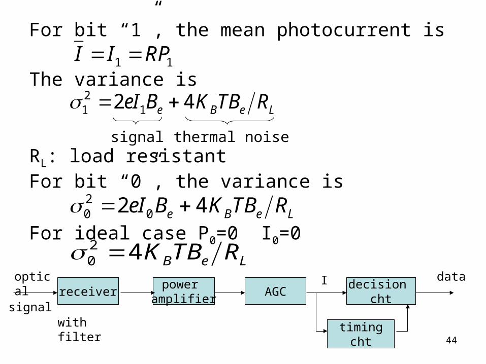
For bit “1”, the mean photocurrent is
The variance is
RL: load resistantFor bit “0”, the variance is
For ideal case P0=0 I0=0
1 1I I RP
20 02 4e B e LeI B K TB R
21 12 4e B e LeI B K TB R
signal thermal noise
20 4 B e LK TB R
receiverpower
amplifierAGC
decision cht
timingcht
optical
signalwithfilter
dataI
45
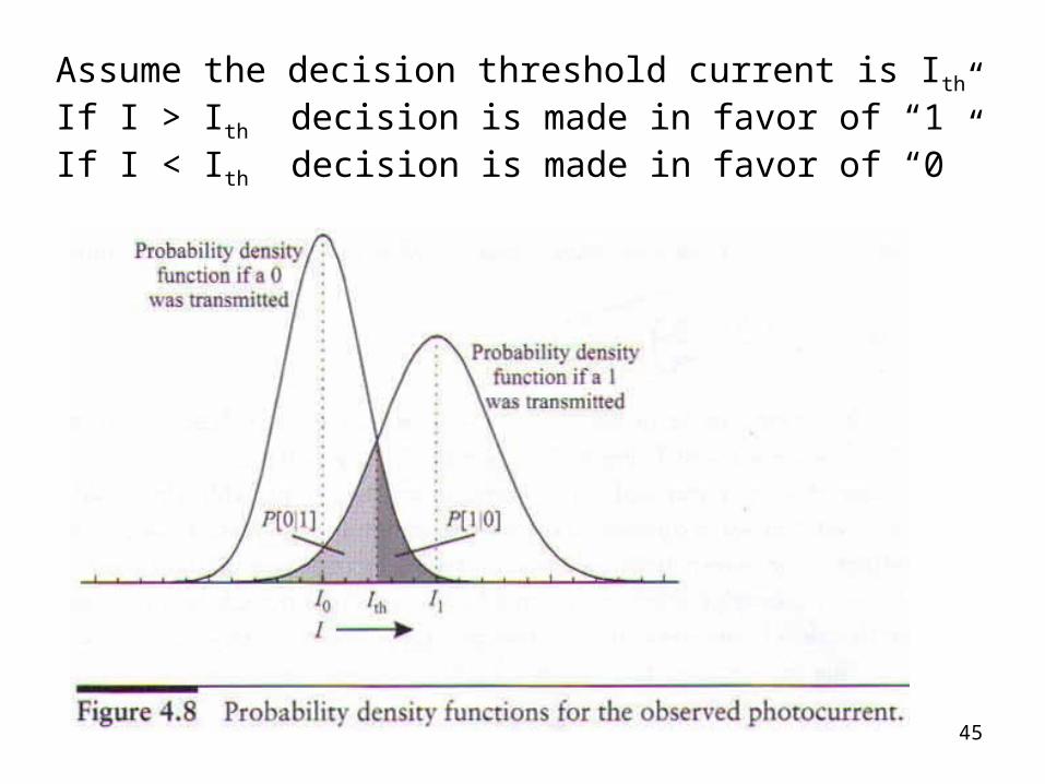
Assume the decision threshold current is Ith If I > Ith decision is made in favor of “1”If I < Ith decision is made in favor of “0”
46
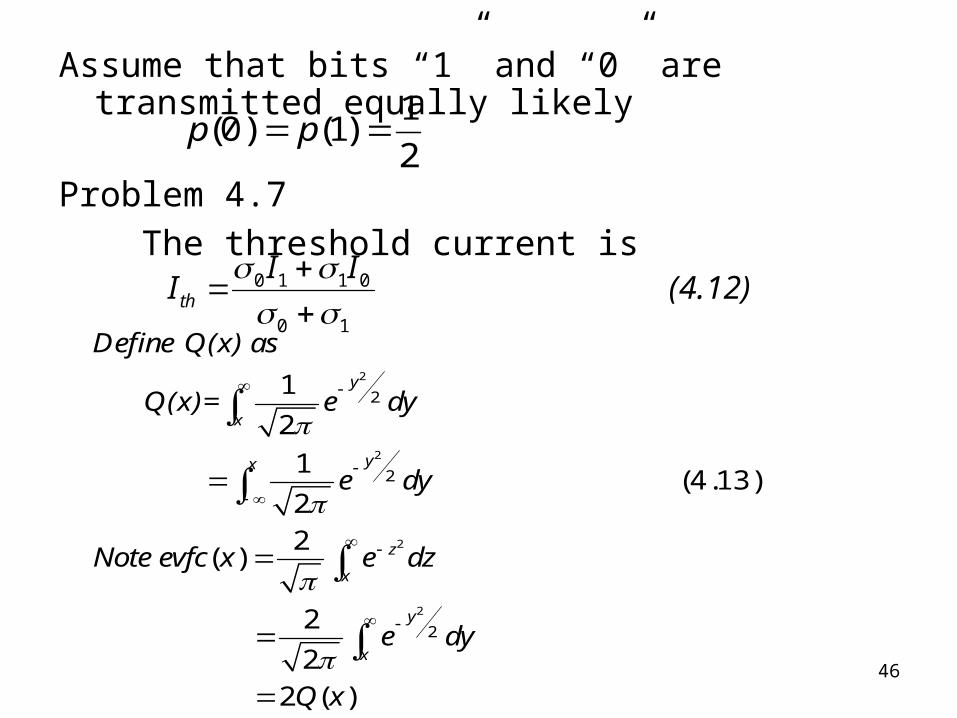
Assume that bits “1” and “0” are transmitted equally likely
Problem 4.7
The threshold current is
1(0) (1)
2p p
(4.12)0 1 1 0
0 1th
I II
Q(x)
Q(x)=2
2
2
2
2
2
2
1
2
1(4.13)
22
( )
2
22 ( )
y
x
yx
z
x
y
x
Define as
e dy
e dy
Note evfc x e dz
e dy
Q x
47
Then we have
P
P
1
1
0
0
0 1
10
th
th
I IQ
I IQ
0 1 1 0
0 1
0 1 1 1 0 1 1 01
0 1
1 1 0
0 1
1 1 0
1 0 1
0 1 1 0 0 0 1 00
0 1
0 1 0
0 1
0 1 0
0 0 1
th
th
th
th
th
Recall
I II
I I I II I
I I
I I I I
I I I II I
I I
I I I I
48
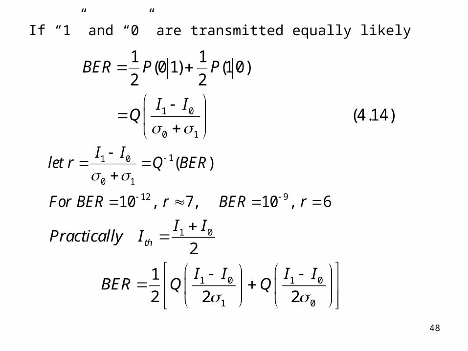
If “1” and “0” are transmitted equally likely
1 0
0 1
1 1(0 1) (10)
2 2
(4.14)
BER P P
I IQ
11 0
0 1
12 9
( )
10 , 7, 10 , 6
I Ilet r Q BER
For BER r BER r
1 0
1 0 1 0
1 0
2
1
2 2 2
th
I IPractically I
I I I IBER Q Q
49
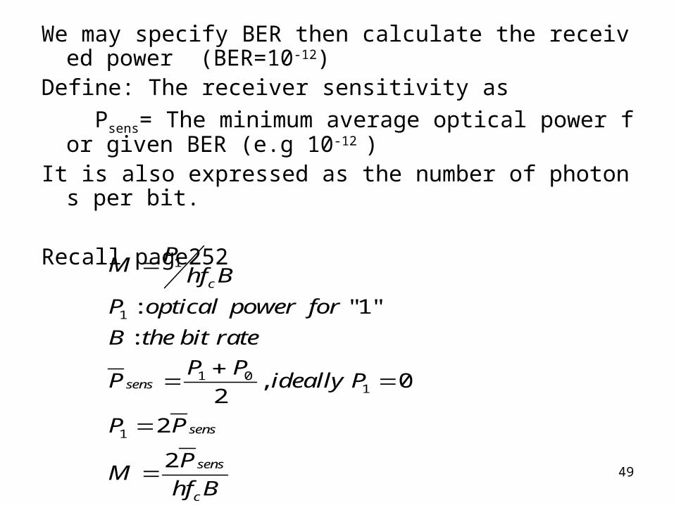
We may specify BER then calculate the received power (BER=10-12)
Define: The receiver sensitivity as
Psens= The minimum average optical power for given BER (e.g 10-12 )
It is also expressed as the number of photons per bit.
Recall page2521
1
1 01
1
: "1"
:
, 02
2
2
c
sens
sens
sens
c
PM hf B
P optical power for
B the bit rate
P PP ideally P
P P
PM
hf B
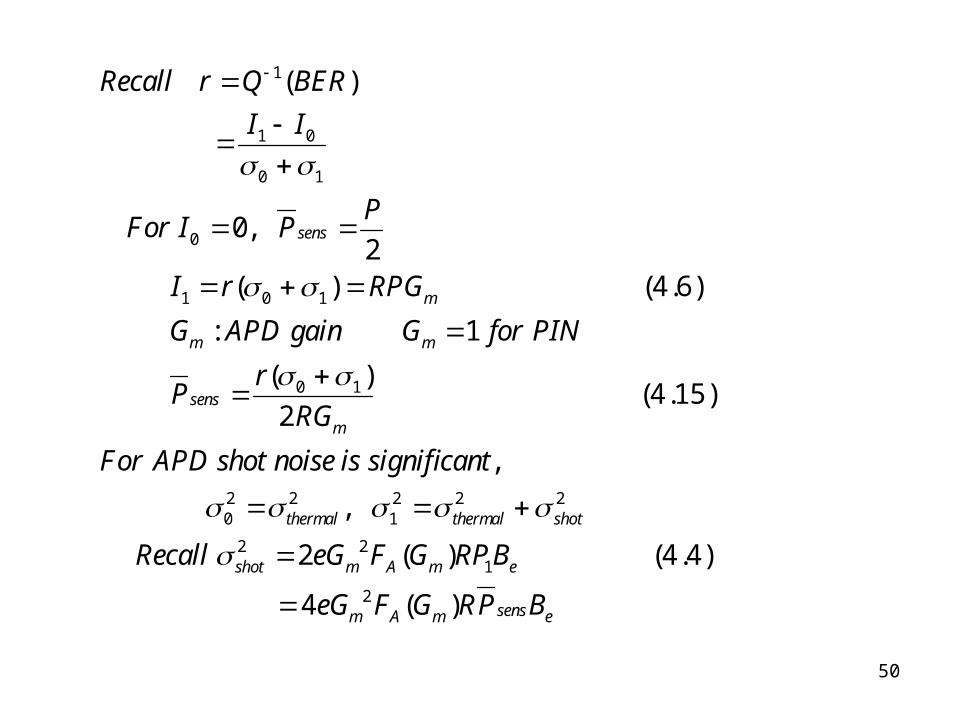
50
1
1 0
0 1
0
1 0 1
0 1
2 2 2 2 20 1
2 21
( )
0,2
( ) (4.6)
: 1
( )(4.15)
2
,
,
2 ( )
sens
m
m m
sens
m
thermal thermal shot
shot m A m e
Recall r Q BER
I I
PFor I P
I r RPG
G APD gain G for PIN
rP
RG
For APD shot noise is significant
Recall eG F G RPB
2
(4.4)
4 ( ) sensm A m eeG F G RP B
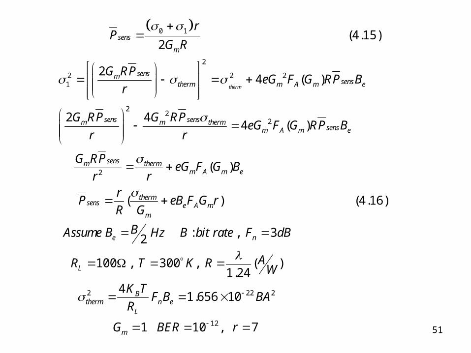
51
0 1
2
2 2 21
22
2
2
(4.15)2
24 ( )
2 44 ( )
( )
(
therm
sens
m
sensmsenstherm m A m e
sens sensm m thermsensm A m e
sensm thermm A m e
thermsens e A m
m
rP
G R
G RPeG F G RP B
r
G RP G RPeG F G RP B
r r
G RPeG F G B
r rr
P eB F GR G
2 22 2
12
) (4.16)
: , 32
100 , 300 , ( )1.24
41.656 10
1 10 , 7
e n
L
Btherm n e
L
m
r
BAssume B Hz B bit rate F dB
AR T K R W
K TF B BA
R
G BER r
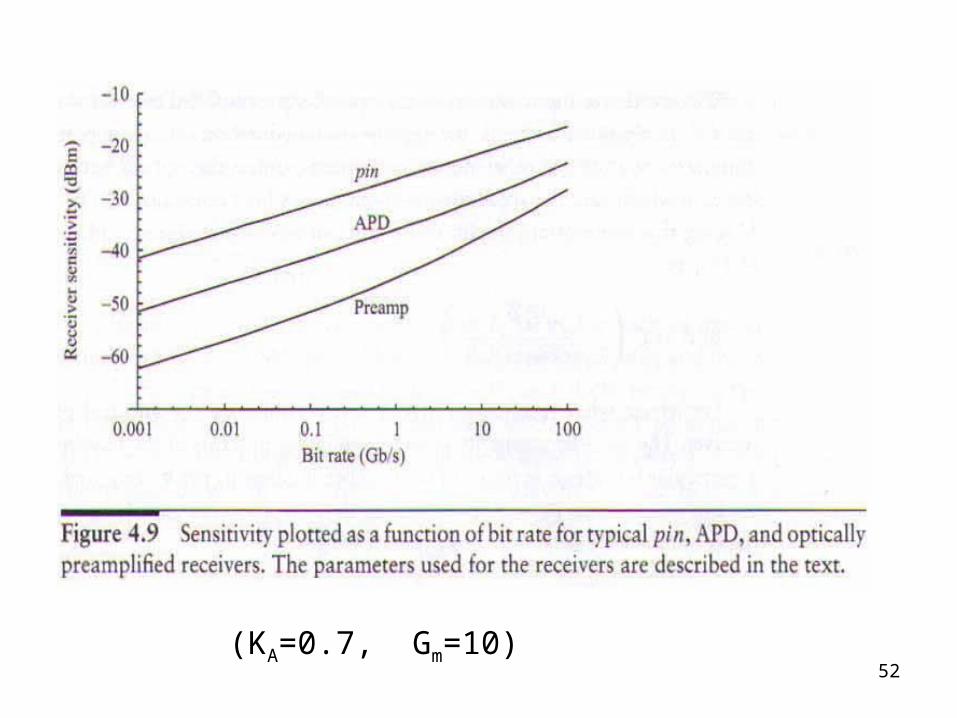
52(KA=0.7, Gm=10)
53
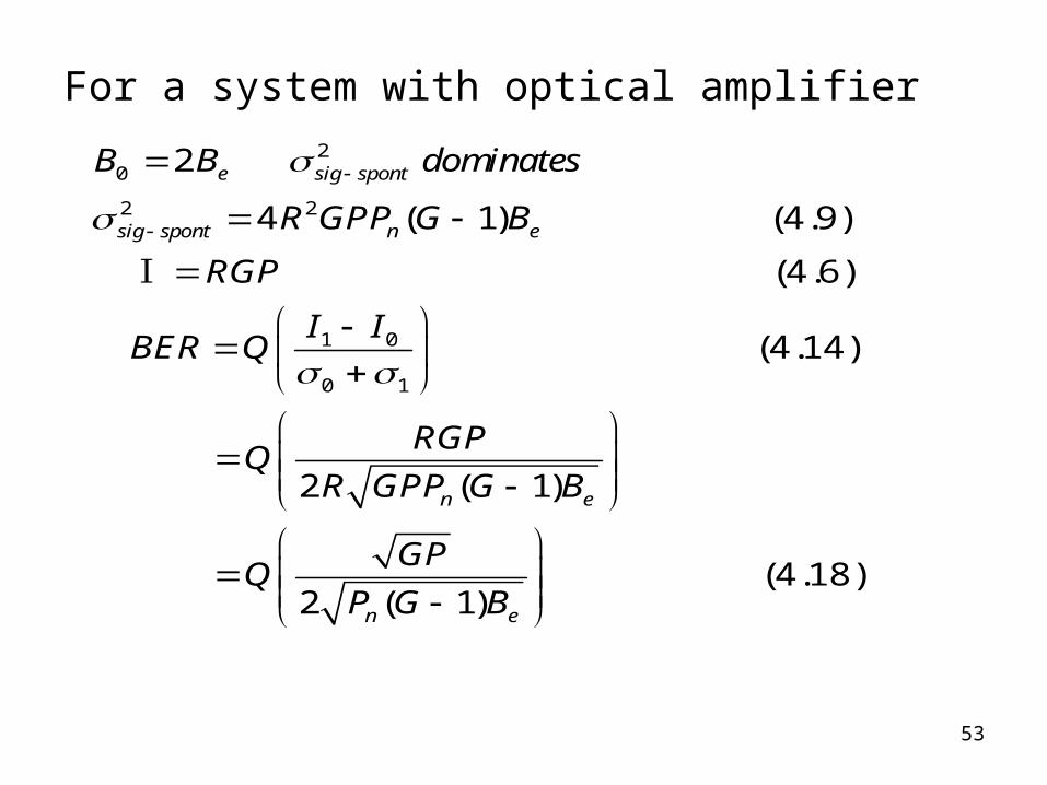
For a system with optical amplifier2
0
2 2
1 0
0 1
2
4 ( 1) (4.9)
(4.6)
(4.14)
2 ( 1)
(4.18)2 ( 1)
e sig spont
sig spont n e
n e
n e
B B dominates
R GPP G B
RGP
I IBER Q
RGPQ
R GPP G B
GPQ
P G B
I
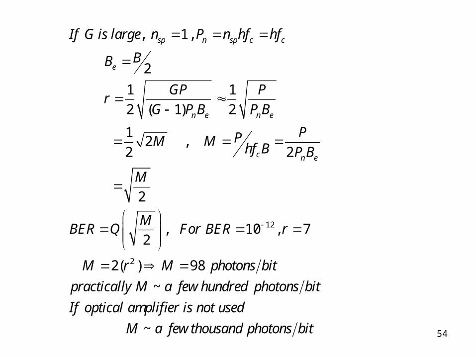
54
12
2
, 1,
2
1 1
2 ( 1) 2
12 ,
2 2
2
, 10 , 72
2( ) 98
~
~
sp n sp c c
e
n e n e
c n e
If G is large n P n hf hf
BB
GP Pr
G P B P B
PPM M hf B P B
M
MBER Q For BER r
M r M photons bit
practically M a few hundred photons bit
If optical amplifier is not used
M a f
ew thousand photons bit
55
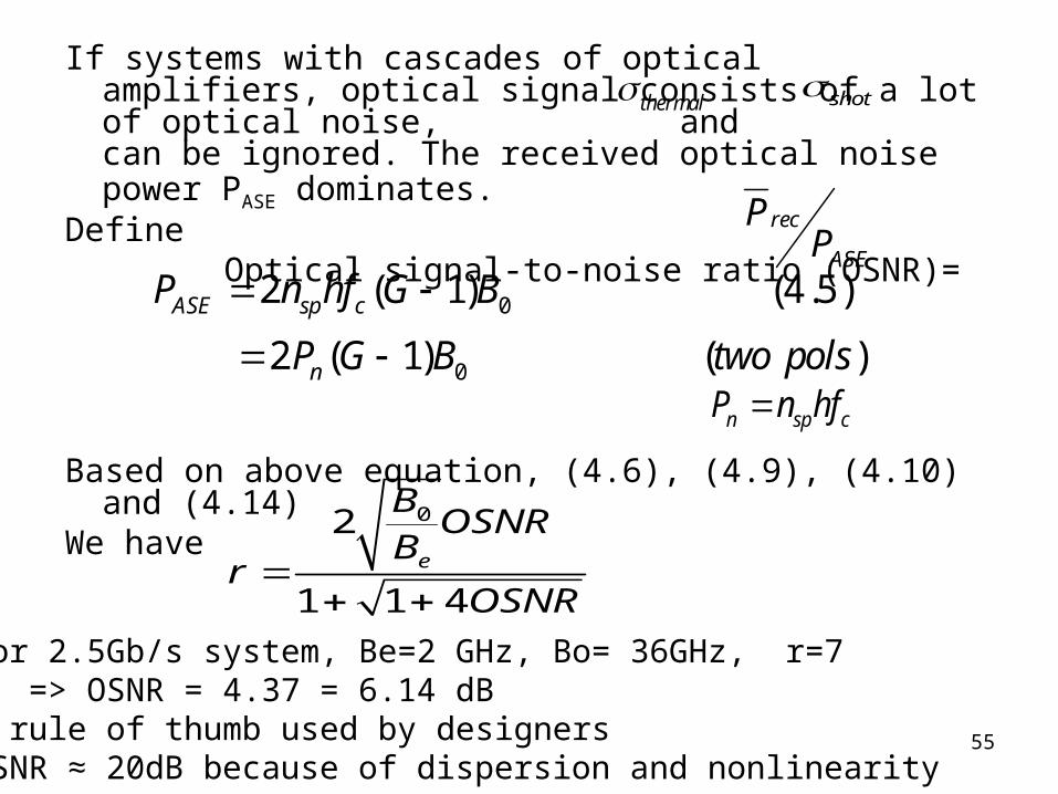
If systems with cascades of optical amplifiers, optical signal consists of a lot of optical noise, and can be ignored. The received optical noise power PASE dominates.
Define Optical signal-to-noise ratio (OSNR)=
Based on above equation, (4.6), (4.9), (4.10) and (4.14)We have
For 2.5Gb/s system, Be=2 GHz, Bo= 36GHz, r=7 => OSNR = 4.37 = 6.14 dBA rule of thumb used by designers OSNR ≈ 20dB because of dispersion and nonlinearity
rec
ASE
PP
0
0
2 ( 1) (4.5)
2 ( 1) ( )
ASE sp c
n
P n hf G B
P G B two pols
02
1 1 4e
BOSNR
Br
OSNR
n sp cP n hf
thermal shot
56
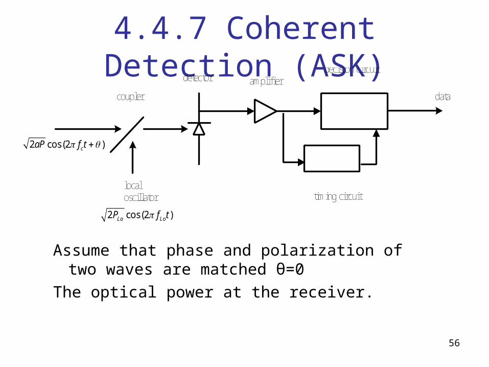
4.4.7 Coherent Detection (ASK)
Assume that phase and polarization of two waves are matched θ=0
The optical power at the receiver.
coupler
detector amplifierdecision circuit
timing circuit
data
localoscillator
2 cos(2 )caP f t
2 cos(2 )Lo LoP f t
57
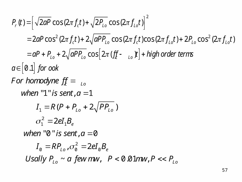
2
2 2
( ) 2 cos(2 ) 2 cos(2 )
2 cos (2 ) 2 cos(2 )cos(2 ) 2 cos (2 )
2 cos 2 ( )
0.1
r c Lo Lo
c Lo c Lo Lo Lo
Lo Lo c Lo
P t aP f t P f t
aP f t aPP f t f t P f t
aP P aPP f f t high order terms
a for ook
1
21 1
20 0 0
"1" , 1
( 2 )
2
"0" , 0
, 2
~ , 0.01 ,
c Lo
Lo Lo
e
Lo e
Lo Lo
For homodyne f f
when is sent a
I R P P PP
eI B
when is sent a
I RP eI B
Usally P a few mw P mw P P
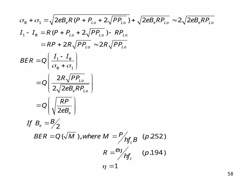
58
0 1
1 0
1 0
0 1
2 ( 2 ) 2 2 2
( 2 )
2 2
2
2 2
2
2
( ), ( .252)
( .194)
1
e Lo Lo e Lo e Lo
Lo Lo Lo
Lo Lo
Lo
e Lo
e
e
c
c
eB R P P PP eB RP eB RP
I I R P P PP RP
RP R PP R PP
I IBER Q
R PPQ
eB RP
RPQ
eB
BIf B
PBER Q M where M phf B
eR phf
59
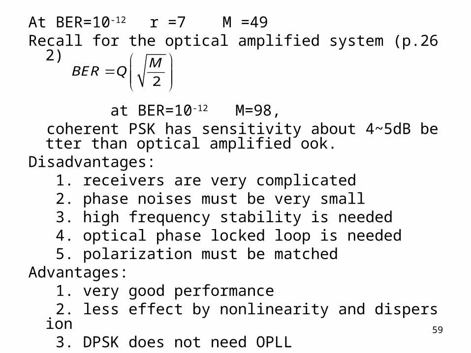
At BER=10-12 r =7 M =49Recall for the optical amplified system (p.262)
at BER=10-12 M=98, coherent PSK has sensitivity about 4~5dB better than opti
cal amplified ook.Disadvantages: 1. receivers are very complicated 2. phase noises must be very small 3. high frequency stability is needed 4. optical phase locked loop is needed 5. polarization must be matchedAdvantages: 1. very good performance 2. less effect by nonlinearity and dispersion 3. DPSK does not need OPLL
2
MBER Q
60
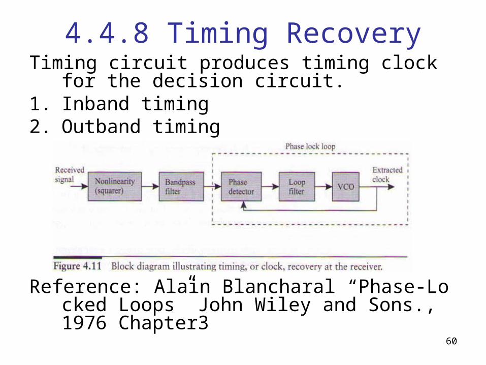
4.4.8 Timing RecoveryTiming circuit produces timing clock for the decisio
n circuit.1. Inband timing2. Outband timing
Reference: Alain Blancharal “Phase-Locked Loops” John Wiley and Sons., 1976 Chapter3
61
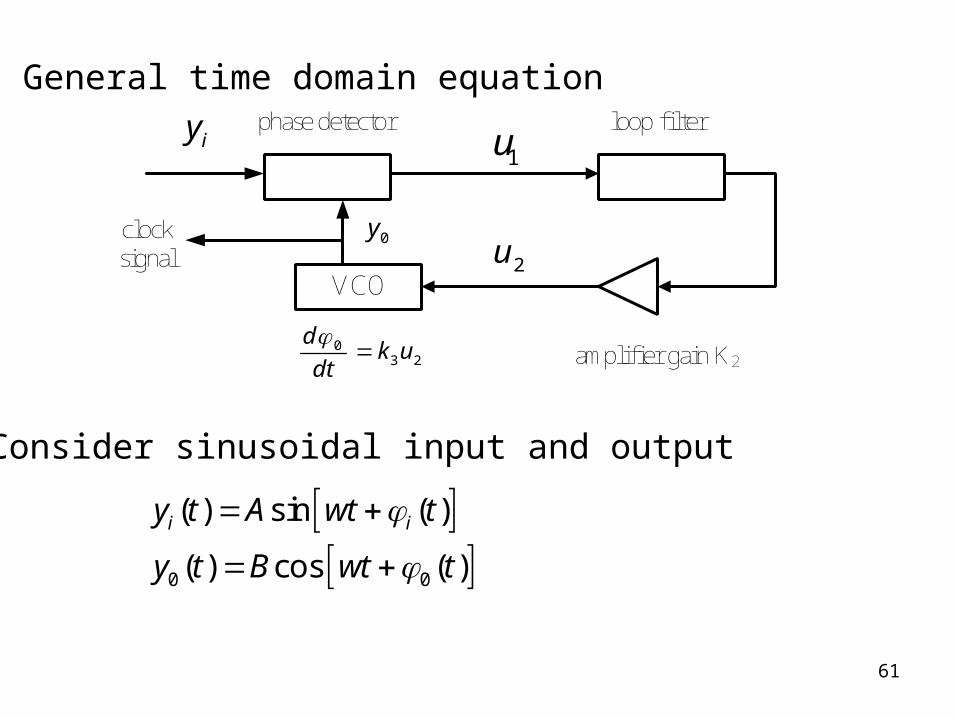
General time domain equation
Consider sinusoidal input and output
0 0
( ) sin ( )
( ) cos ( )
i iy t A wt t
y t B wt t
VCO
iy phase detector
1uloop filter
amplifier gain K2
2u0yclock
signal
03 2
dk u
dt
62
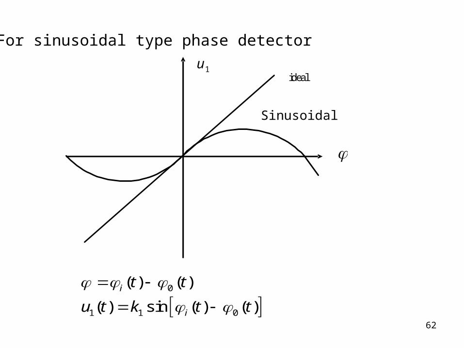
For sinusoidal type phase detector
1uideal
0
1 1 0
( ) ( )
( ) sin ( ) ( )i
i
t t
u t k t t
Sinusoidal
63
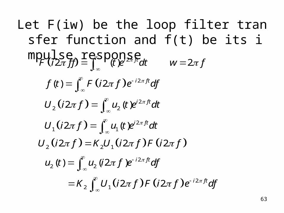
Let F(iw) be the loop filter transfer function and f(t) be its impulse response
2
2
22 2
21 1
2 2 1
22 2
22 1
2 ( ) 2
( ) 2
2 ( )
2 ( )
2 2 2
( ) ( 2 )
2 2
i ft
i ft
i ft
i ft
i ft
i ft
F i f f t e dt w f
f t F i f e df
U i f u t e dt
U i f u t e dt
U i f K U i f F i f
u t u i f e df
K U i f F i f e df
64
1
2 22 2 1
2 ( )2 1
2
( ) ( ) ( 2 )
( ) ( 2 )
( ) ( )
i f i ft
i f t
u t K u e d F i f e d
K u F i f e dfd
K u f t d
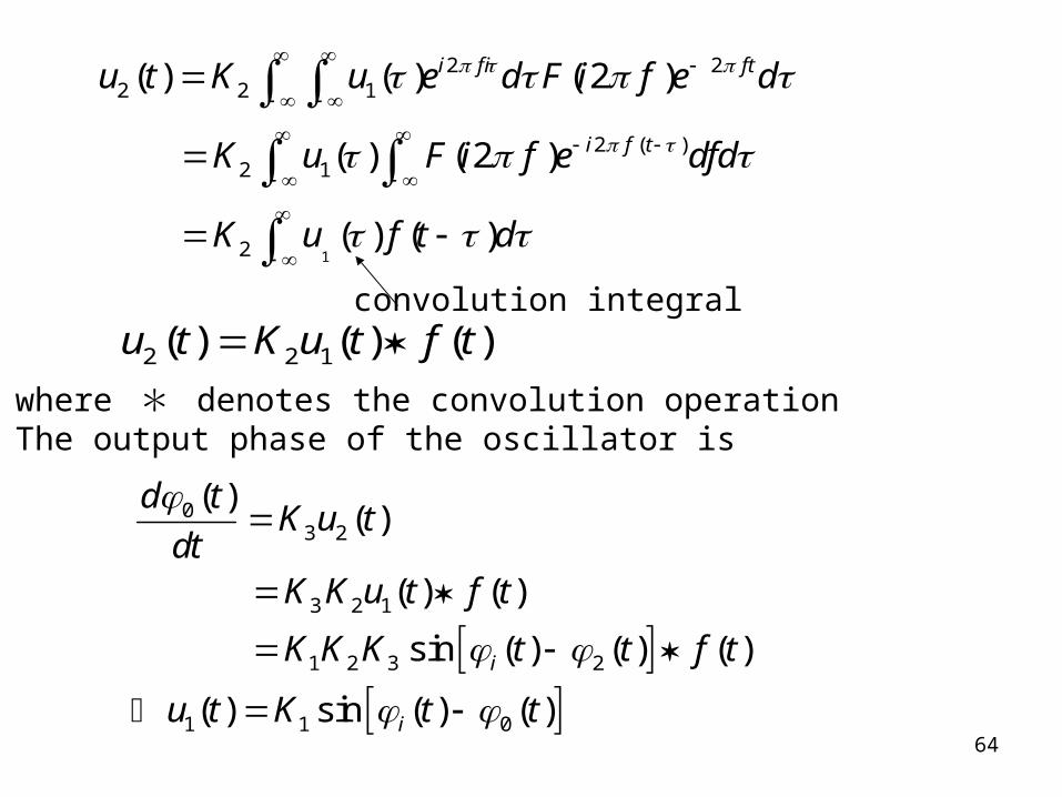
2 2 1( ) ( ) ( )u t K u t f t where * denotes the convolution operationThe output phase of the oscillator is
03 2
3 2 1
1 2 3 2
1 1 0
( )( )
( ) ( )
sin ( ) ( ) ( )
( ) sin ( ) ( )
i
i
d tK u t
dtK K u t f t
K K K t t f t
u t K t t
convolution integral
65
1 2 3
00
0 0
0
00
20 0
2
0
( )sin ( ) ( ) ( )
sin ( ) ( ) ( ) ( )
( ) ( )
( )( ) ( ) ( )
( 2 ) ( )
( 2 ) ( )
(
i
i i
i
i
ft
fti i
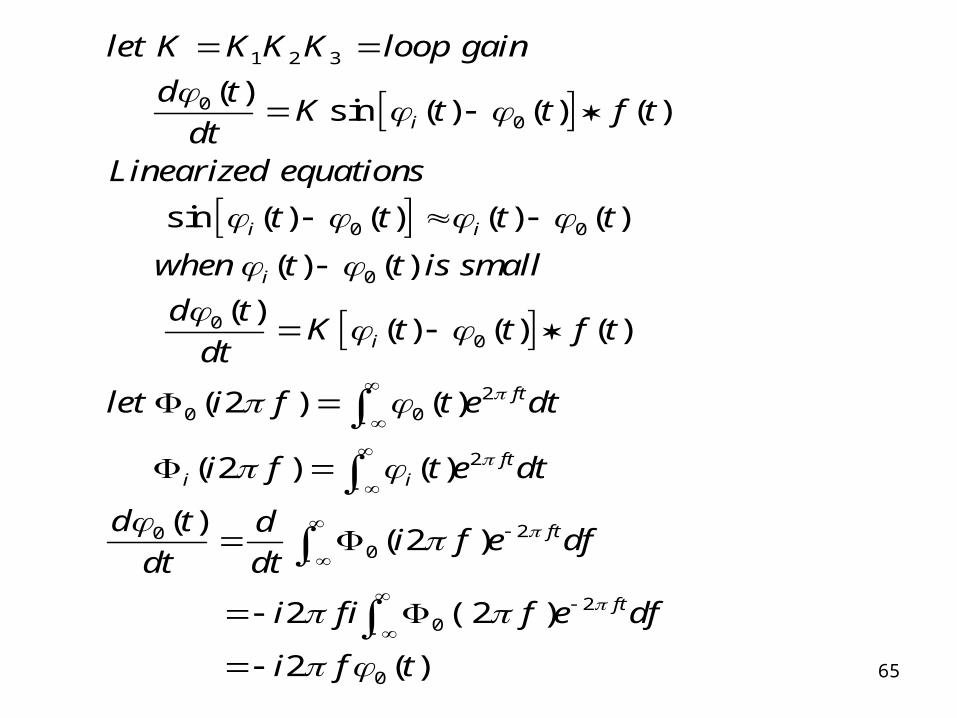
let K K K K loop gain
d tK t t f t
dtLinearized equations
t t t t
when t t is small
d tK t t f t
dt
let i f t e dt
i f t e dt
d t
20
20
0
)( 2 )
2 ( 2 )
2 ( )
ft
ft
di f e df
dt dt
i f i f e df
i f t
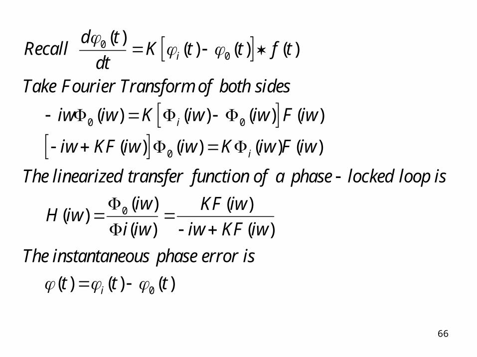
66
00
0 0
0
0
( )( ) ( ) ( )
( ) ( ) ( ) ( )
( ) ( ) ( ) ( )
( ) ( )( )
( )
i
i
i
d tRecall K t t f t
dtTake Fourier Transform of both sides
iw iw K iw iw F iw
iw KF iw iw K iw F iw
The linearized transfer function of a phase locked loop is
iw KF iwH iw
i iw iw
0
( )
( ) ( ) ( )i
KF iw
The instantaneous phase error is
t t t
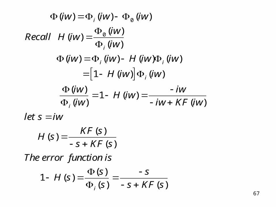
67
0
0
( ) ( ) ( )
( )( )
( )
( ) ( ) ( ) ( )
1 ( ) ( )
( )1 ( )
( ) ( )
( )( )
( )
( )1 ( )
( ) ( )
i
i
i i
i
i
i
iw iw iw
iwRecall H iw
iw
iw iw H iw iw
H iw iw
iw iwH iw
iw iw KF iw
let s iw
KF sH s
s KF s
The error function is
s sH s
s s KF s
68
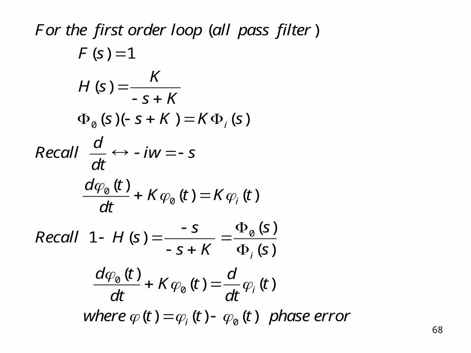
0
00
0
00
0
( )
( ) 1
( )
( )( ) ( )
( )( ) ( )
( )1 ( )
( )
( )( ) ( )
( ) ( ) ( )
i
i
i
i
i
For the first order loop all pass filter
F s
KH s
s Ks s K K s
dRecall iw s
dtd t
K t K tdt
ssRecall H s
s K s
d t dK t t
dt dtwhere t t t phase error
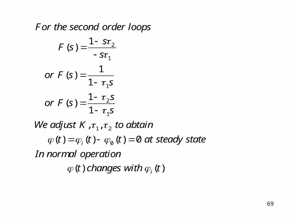
69
2
1
1
2
1
1 2
0
1( )
1( )
1
1( )
1
, ,
( ) ( ) ( ) 0
( ) ( )
i
i
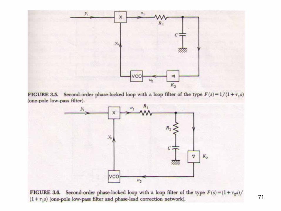
For the second order loops
sF s
s
or F ss
sor F s
s
We adjust K to abtain
t t t at steady state
In normal operation
t changes with t
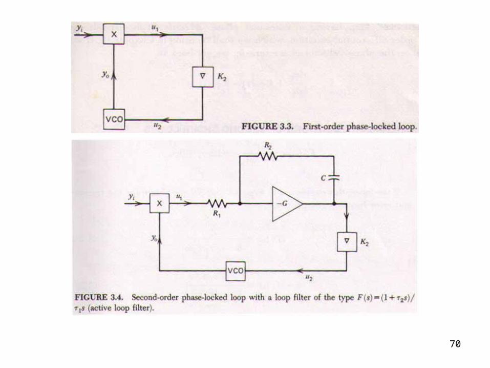
70
71
72
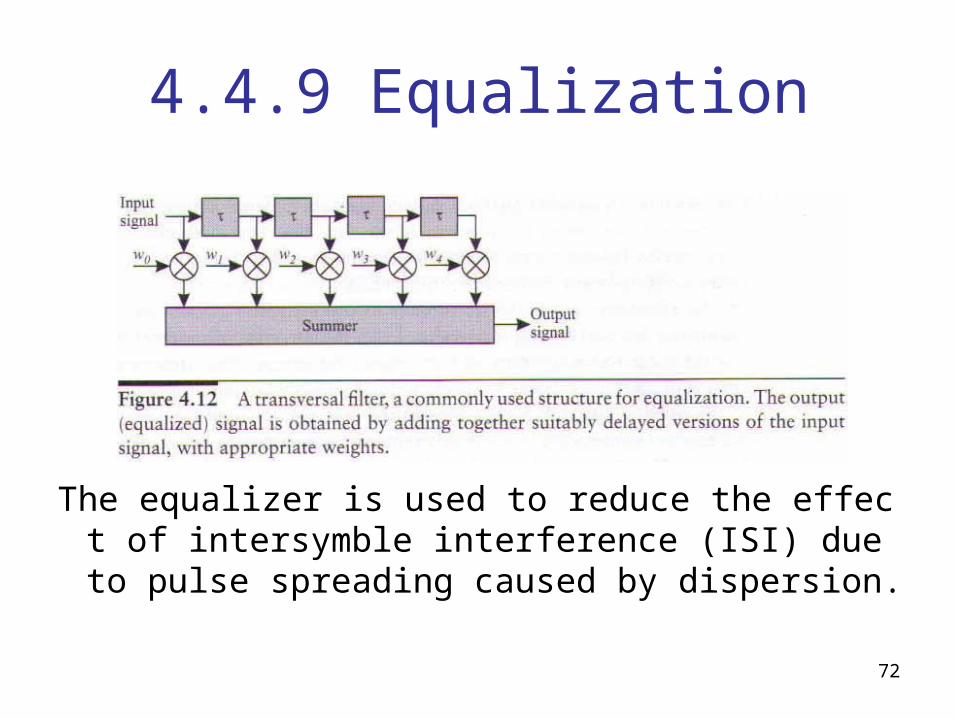
4.4.9 Equalization
The equalizer is used to reduce the effect of intersymble interference (ISI) due to pulse spreading caused by dispersion.