Embed Size (px)
Citation preview

1
Design of a High-Performance High-Pass
Generalized Integrator Based Single-Phase PLLAbhijit Kulkarni and Vinod John
Abstract
Grid-interactive power converters are normally synchronized to the grid using phase-locked loops (PLLs). The
performance of the PLLs is affected by the non-ideal conditions in the sensed grid voltage such as harmonics,
frequency deviations and dc offsets in single-phase systems. In this paper, a single-phase PLL is presented to mitigate
the effects of these non-idealities. This PLL is based on the popular second order generalized integrator (SOGI)
structure. The SOGI structure is modified to eliminate of the effects of input dc offsets. The resulting SOGI structure
has a high-pass filtering property. Hence, this PLL is termed as high-pass generalized integrator based PLL (HGI-
PLL). It has fixed parameters which reduces the implementation complexity and aids in the implementation in low-end
digital controllers. The HGI-PLL is shown to have least resource utilization among the SOGI based PLLs with dc
cancelling capability. Systematic design methods are evolved leading to the design that limits the unit vector THD to
within 1% for given non-ideal input conditions in terms of frequency deviation and harmonic distortion. The proposed
designs achieve the fastest transient response. The performance of this PLL has been verified experimentally. The
results are found to agree with the theoretical prediction.
Index Terms
Phase-locked loops, distributed generation, dc offsets, current control, harmonic distortion.
NOMENCLATURE
PLL Phase-locked loop.
SOGI Second-order generalized integrator.
SRF Synchronous reference frame.
HGI High-pass generalized integrator.
k Gain in the HGI transfer functions.
ω0 Nominal grid frequency (2π50 rad/s).
vg Sensed grid voltage.
The authors are with the Department of Electrical Engineering, Indian Institute of Science, Bangalore - 560012. They can be contacted through
email at: [email protected] and [email protected].
A Kulkarni is presently affiliated with the Department of Electrical and Computer Engineering, University of Illinois at Chicago, Chicago IL
60607, USA.
arX
iv:1
609.
0411
4v1
[cs
.SY
] 1
4 Se
p 20
16

2
vα, vβ In-phase and quadrature-phase outputs of HGI with vg as the input.
vd, vq Rotating reference frame voltages corresponding to SRF transformation of vα, vβ .
kp, ki Proportional and integral gains of the PI controller.
ωe Estimated frequency of the HGI-PLL in rad/s.
θe Estimated phase of the HGI-PLL in rad.
ts,srf Settling time due to the embedded SRF-PLL in HGI-PLL.
ts,hgi Settling time due to the HGI block.
tsd Additive worst case settling time
(tsd = ts,srf + ts,hgi).
ωbw Design bandwidth of the embedded SRF-PLL in rad/s.
fbw Design bandwidth of the embedded SRF-PLL in Hz.
kopt,h Optimum value of k in HGI that gives the fastest settling time.
U Design limit on the unit vector THD in %.
∆f Maximum frequency deviation considered in grid (∆f = ±8%).
uthd Unit vector THD in %.
Ku Set of k satisfying uthd ≤ 1% for any given fbw.
I. INTRODUCTION
Phase-locked loops (PLLs) are used in multiple applications: from miniature system on chip (SOC) to large
grid-connected power converters. In SOCs, the PLLs are used for functions such as clock generation [1]. In grid-
connected power converters such as distributed generation (DG) systems and static compensators (STATCOMs),
PLLs are used for synchronization with the grid voltage [2]–[7]. In this paper, the design and implementation
aspects for PLL in single-phase grid connected power converters are discussed.
The PLLs estimate the frequency, phase and amplitude of the grid voltage. They are used to generate unit
amplitude sine and cosine signals synchronized with the grid voltage. These signals are called unit vectors [8].
They are used for the reference signal generation in the closed-loop control of the power converters. The PLLs are
also used to monitor the disturbances in the grid voltage [4], [9]–[11]. Fig. 1 shows the general schematic of a PLL
used in the grid-synchronization of a single-phase power converter.
Vg VoltageSensor
PLL
ωe θe Vm
sinθe
cosθe
Fig. 1. General structure of a PLL used in a grid-connected power converter. Vg is the grid voltage. ωe, θe and Vm are the frequency, phase
and amplitude of grid voltage estimated by the PLL. sin θe and cos θe are the unit vectors.

3
The performance of the single-phase PLLs is affected by the non-ideal conditions in the grid voltage. These are:
frequency deviation, harmonic distortion and dc offsets. In case of three-phase systems, there will be an additional
non-ideality of unbalance in the three-phase voltages. It must be noted that under ideal conditions, the grid voltage
has fixed frequency of either 50/60Hz, no harmonic distortion, no dc offsets and no unbalance in three-phase case.
A. Literature Survey of Existing PLL Structures
Among the various PLLs proposed in literature, synchronous reference frame PLL (SRF-PLL) is a popular
PLL [8], [12] used in three-phase systems. It is very simple from design and implementation point of view. SRF-PLL
forms the building block of many PLLs for both three-phase and single-phase applications [13]–[19]. Second-order-
generalized-integrator (SOGI) based single-phase PLLs [16]–[19] are low-complexity single-phase PLLs that use an
embedded SRF-PLL. The basic SOGI-PLL was first introduced in [16]. This PLL will have sinusoidal ripple errors
in the estimated frequency when the input contains harmonics and dc offsets. These ripple errors can also occur
when the input frequency changes from the nominal value [16]. Adaptation of the SOGI parameters is suggested
to overcome the problem due to input frequency deviation [16], [17], [19], [20]. The adaptive SOGI-PLLs have
higher design and implementation complexity.
Input to the single-phase SOGI based PLLs can have a dc offset due to factors such as sensor dc offsets, dc
offsets from the analog-to-digital controllers (ADC) and mismatch in the semiconductor device switching in practical
power converters. As the basic SOGI structure cannot eliminate dc offsets, the embedded SRF-PLL will have a dc
offset in its input. This can result in a serious problem of dc injection to the grid [21]. DC injection to the grid is
undesired [22] and it is to be limited to be less than 0.5% of the rated current of the power converter as per the
grid interconnection standard IEEE 1547-2003 [23].
The problem of dc offsets in the basic SOGI-PLL is mitigated in [17], where the design method is based on
heuristic approach. Also, the effect of input harmonics is not quantified in the work. Multiple cascaded SOGI based
frequency locked loop (FLL) is proposed in [24]. This is proposed for three-phase systems. Design optimizations
considering the response time have not been analyzed. Cascading of the SOGI blocks increases the implementation
complexity in terms of increased computation time or digital resource utilization. In [25], a modified high-pass based
SOGI structure is studied for a robust adaptive PLL. This PLL contains additional non-linear functions compared
to other SOGI based PLLs such as [16]–[19] and the response to transients reported in the paper is slow in the
order of tens of fundamental cycles. The work in [26] estimates the grid frequency and amplitude correctly when
the input contains dc offsets. However, the phase estimation is affected by the input dc offsets.
B. Present Work
In this paper, a modified SOGI-PLL is presented. The modified SOGI has full dc offset rejection capability and
includes a high-pass based filter structure. Hence, this PLL is termed as high-pass generalized integrator based PLL
(HGI-PLL). The outputs of the HGI are given as inputs to the embedded SRF-PLL block.

4
vq
vd
vd*=0
SineTable
vgαβ/dq
UnitVectors
k―
―
― vα
vβ
ff
-1
vβ2
High-pass based SOGI Embedded SRF-PLL
kp+(ki/s)PI controller
Fig. 2. Structure of high-pass generalized integrator based PLL (HGI-PLL).
The structure of the HGI-PLL is shown in Fig. 2. This is a fixed parameter or non-adaptive PLL which helps to
keep its implementation simple. Its performance is affected by the frequency deviations as well as harmonics in the
input voltage. These non-ideal conditions of frequency deviations and harmonics result in unit vector harmonic
distortion [18]. This is undesirable as the unit vectors are used for reference generation and are expected to
have minimal harmonic distortion. Hence, the HGI-PLL must be designed such that the the unit vector distortion
is minimal for the non-ideal grid conditions of frequency deviation and harmonic distortion. Another desirable
performance parameter is the fast settling time. The HGI-PLL design must consider these factors of minimal unit
vector distortion and fast response time for given worst case non-idealities in the grid voltage.
Novel systematic designs are evolved for the HGI-PLL in this paper. For a given worst case frequency deviation
in the input, a design approach is proposed which results in the fastest response for a given constraint on the
unit vector THD. For example, for a worst case setting of ±8% frequency deviation, the HGI-PLL is designed to
have fastest response while limiting the unit vector THD to be less than 1%. This design is evolved into a design
procedure considering two constraints, namely, the worst case frequency deviations and harmonic distortions in the
input. This design achieves fastest response for HGI-PLL while limiting the unit vector THD to be within 1% for
the given worst-case input conditions.
The HGI-PLL with the proposed designs achieves very good transient and steady-state performance. The practical
settling time is shown to be less than 30ms. This PLL has the least resource utilization in the digital implementation
among the SOGI based PLLs with dc cancelling capability. The performance of this PLL has been compared with
analysis and simulation and is validated using experimental results for various steady-state and transient operating
conditions.
II. STRUCTURE AND DESIGN CONSIDERATIONS OF HGI-PLL
A. Structure
The HGI-PLL produces two quadrature signals vα and vβ from the input sensed grid voltage vg . The HGI is
a modified SOGI filter structure which generates vα and vβ . The transfer functions realized by the HGI are as

5
follows.
Gα,h(s) =vαvg
=ksω0
s2 + kω0s+ ω20
(1)
Gβ,h(s) =vβvg
= − ks2
s2 + kω0s+ ω20
(2)
It can be verified that both the transfer functions in (1) and (2) have zero gain at dc. When the input voltage is
sinusoidal with frequency ω0, it can be seen that the vα and vβ are balanced quadrature signals. This is evident
from the bode plots of the two transfer functions in Fig. 3.M
agni
tude
(dB
)
−40
−20
−0
20Gα,h(s) Gβ,h(s)
Phas
e (d
eg.)
−200
−100
0
100
Frequency (rad/s)10 100 1,000 10,000
Fig. 3. Bode plot of the transfer functions of HGI-PLL when k = 1.6.
As it can be seen from Fig. 3, the transfer function in (2) is a high-pass filter. In a basic SOGI-PLL [16], the
transfer function to generate vβ is a low-pass filter. Hence, it does not block any dc offset in the input voltage. As
a result, the embedded SRF-PLL will have dc offsets in its input which in turn lead to dc offsets in the PLL unit
vectors [21]. In HGI-PLL, this is mitigated by making use of a dc blocking high-pass filter as shown in Fig. 2.
B. Design Considerations
The HGI-PLL has three design parameters: the gain k in the HGI transfer functions, kp and ki of the PI controller
transfer function as shown in Fig. 2. In adaptive SOGI based PLLs, the term ω0 used in the transfer functions is
replaced by the estimated frequency ωe of the PLL [20]. In the present implementation, ω0 is constant and is
equal to the nominal grid frequency in rad/s. By keeping ω0 fixed, the implementation is simplified. Use of fixed
parameters helps in arriving at a systematic design method and hence the response time can be optimized.
The main disadvantage of fixed parameter SOGI based PLLs is the fact that frequency deviations in the input
voltage will cause unequal amplitudes in the vα and vβ . This is clear from Fig. 3 also. The unequal amplitudes result
in the application of a negative sequence component to the embedded SRF-PLL [18]. This results in double harmonic
ripple in the estimated frequency [12] and hence, harmonic distortion in the unit vectors [8]. Harmonic distortion

6
in the unit vectors is highly undesirable because the current references generated using them will also become
distorted. As the current controllers used normally have low-pass filtering characteristics with high bandwidth [27],
the resulting grid current will be distorted. Grid interconnection standards such as IEEE 1547-2003 [23] have defined
limits on the harmonic injection to the grid. The PLL design should ensure that these limits are not exceeded. This
can be achieved by carefully selecting the bandwidth of the embedded SRF-PLL. Lower the bandwidth, better will
be the harmonic attenuation for the unit vectors when the input has frequency deviations [18]. The response time
of the embedded SRF-PLL is inversely related to its bandwidth. The relation between settling time ts,srf and its
bandwidth ωbw in rad/s can be approximated as [21],
ts,srf = 4/ωbw (3)
There is a tradeoff between the response time and harmonic attenuation. Hence, it is important to arrive at a design
bandwidth of the embedded SRF-PLL such that the response time is fastest for a given constraint on the unit vector
harmonic distortion or THD. This approach of the PLL parameter design is followed for the basic SOGI-PLL
in [18].
When the grid voltage has transient amplitude or phase jumps, the filters used in the HGI will take a known
amount of time to settle. The transients in the HGI output will affect the inputs vα and vβ to the embedded SRF-
PLL. This results in temporary errors in estimation of frequency and phase till the HGI outputs settle to the correct
values. Hence, the overall settling time is also dependent on the design parameter k of the HGI block. It must be
designed to have a fast response during transient changes in the grid voltage. Let the overall settling time due to
the HGI transfer functions be defined as,
ts,hgi = max(tsα(k), tsβ(k)) (4)
In (4), tsα(k) and tsβ(k) are the settling times of the transfer functions in (1) and (2) for step change. These settling
time values depend on the parameter k.
As the HGI-PLL has a cascade of the HGI block and embedded SRF-PLL block, the worst-case additive settling
time is given by the sum of the settling times of the HGI blocks and the embedded SRF-PLL. This worst-case
additive settling time is termed as tsd and it is given by,
tsd = ts,hgi + ts,srf (5)
The grid voltage at the point of common coupling (PCC) normally contains lower order harmonics due to the
presence of non-linear loads in the system and finite grid impedance [28], [29]. The transfer function in (1) has
bandpass configuration centred around nominal fundamental frequency ω0. Hence, there will be attenuation of
harmonics by this transfer function. However, as it can be seen from Fig. 3, the transfer function (2) has high-pass
characteristic and hence it cannot attenuate any harmonics in the input. The embedded SRF-PLL has a low-pass
characteristic and can attenuate the harmonics. Hence, to sufficiently attenuate the input harmonics, both k and PI
controller parameters of the embedded SRF-PLL will have to be selected carefully as proposed in Section III of
the paper. This also has an effect on the overall settling time, which is to be minimized as explained in Section III.

7
Sett
ling
time
(s)
0
0.05
0.1
0.15
0.2
0.25
k0.5 1 1.5 2 2.5 3 3.5
For Gα,h (s)For Gβ,h (s)
0.1
kopt,h
Fig. 4. Variation of settling time of the HGI transfer functions versus k for MTSD design.
III. DESIGN OF THE HGI-PLL
The design of HGI-PLL discussed in the following subsections III-A will be referred to as as minimum tsd
design (MTSD design). Note that tsd is the additive settling time defined in (5) which is the sum of settling time
of the HGI block and the settling time of embedded SRF-PLL block. This design selects the values of k and
bandwidth considering the expected range of frequency deviations alone. The objective of this design is to select
the PLL parameters that lead to shortest additive settling time for a specified limit on unit vector THD considering
worst case frequency deviations in the input. This design is analyzed for its harmonic attenuation capability and the
resulting limitations are then explained. The MTSD design forms the basis for a complete design method proposed
in Section III-B. This is called as harmonic constrained minimum tsd design (HC-MTSD design), because the design
parameters are selected to achieve a limit on the unit vector THD when the input contains both frequency deviation
and harmonic distortion. In other words, this design optimizes the response time of HGI-PLL without exceeding the
THD limit on the unit vectors when the input voltage contains both frequency deviations and harmonic distortion.
A. MTSD Design for HGI-PLL
1) Selection of the parameter k for MTSD design: The parameter k is selected such that the transfer functions
of HGI-PLL give the fastest settling time. The step response settling time of the transfer functions (1) and (2) as a
function of k is determined using simulation. The variation of k with 2% step-response settling time [30] for HGI-
PLL is shown in Fig. 4. As it can be observed, there is a value of k that gives the fastest response, corresponding
to the minimum settling time of the SOGI block in Fig. 2.
From Fig. 4, the optimal value of k is determined to be,
kopt,h = 1.56 (6)
For this value of kopt,h, the settling times for vα and vβ are 14.91ms and 15.97ms respectively for a 50Hz system.
Hence, the combined worst-case settling time (ts,hgi) would be the maximum of the two settling times, that is,
ts,hgi = 15.97ms ≈ 16ms (7)
Thus the worst case settling time of 16ms is less than one fundamental cycle.
8
Selection of k = kopt,h results in the fastest response of the HGI blocks for any changes in the input. The harmonic
attenuation will be fixed based on the selected value of k. The remaining design parameter is the bandwidth of the
embedded SRF-PLL.
2) Selection of the bandwidth of embedded SRF-PLL for MTSD design: As explained in Section II-B, the
frequency deviations in the input result in unit vector distortion. To minimize the unit vector THD, the approach is
to adjust the bandwidth of the SRF-PLL to attenuate the resulting ripple in the vd and estimated frequency. Let the
limit on the unit vector THD be U = 1%. Hence, for a given frequency deviation of ∆f , the SRF-PLL bandwidth
must be chosen to be such that the unit vector THD is uTHD ≤ U (%).
The analytical expressions derived in [8] are used to determine the unit vector THD as a function of the bandwidth
of the embedded SRF-PLL for any frequency deviation in the input. The relevant expressions derived in [8] are
included in Appendix A for quick reference. The procedure to determine the design bandwidth is given in the
flowchart in Fig. 5. The frequency range is swept from fi = [fl, fh]. For a frequency deviation of ∆f = ±8%, the
frequency is swept between fl = 46Hz and fu = 54Hz in a 50Hz system. Step size of 2Hz has been used to
sweep this range.
Fig. 5. Flowchart to determine the design bandwidth of the embedded SRF-PLL for different levels of frequency deviations in the input.
This method is illustrated in Fig. 6. Consider when the input frequency is 46Hz. The equations (21)–(23) in
Appendix A are used and the unit vector THD versus bandwidth are plotted in Fig. 6. The highest bandwidth is

9
0
0.5
1
1.5
2
0 50 100 150 200 250 300
f=46Hz f=48Hz f=52Hz f=54Hz
Bandwidth of embedded SRF-PLL (Hz)
Uni
t ve
ctor
TH
D (
%)
Fig. 6. Variation of unit vector THD with bandwidth for various grid frequency values assuming sinusoidal grid voltage for HGI-PLL.
chosen for this case as per the flowchart to give a unit vector THD of at most U = 1%. This corresponds to the
design bandwidth of 55Hz. Similarly, the bandwidth is determined for the remaining three cases in Fig. 6. It can
be observed from the Fig. 6 that the bandwidth must be chosen to be 55Hz so that the unit vector THD is less
than 1% for the entire range of frequency deviations from 46Hz to 54Hz.
Thus, the bandwidth ωbw,d = 2π55 rad/s will limit the unit vector THD to be less than 1% even for a frequency
deviation of upto ±8% in the input voltage. Once the design bandwidth is known, the PI controller parameters of
the embedded SRF-PLL can be determined using the design equations given in works such as [12], [21]. The final
expressions (33) and (34) used to compute these PI controller parameters are provided in Appendix C. The settling
time of the embedded SRF-PLL for this design bandwidth is given by,
ts,srf = 4/ωbw,d = 11.6ms (8)
3) Summary of the MTSD design: The k in the HGI transfer functions is selected to achieve the fastest response.
The bandwidth of the embedded SRF-PLL is the highest for given frequency deviation and constraint on unit vector
THD. Hence for the given constraints, the embedded SRF-PLL also has the fastest response. The net worst-case
additive settling time using (7) and (8) is given by,
tsd = ts,hgi + ts,srf = 16ms+ 11.6ms = 27.6ms (9)
Thus the proposed design results in a worst-case settling time of less than 1.5 fundamental cycles. The actual
settling time is lesser than this value as the transients in HGI and embedded SRF-PLL occur simultaneously. This
is shown in the Section V with experimental results.
4) Effect of input harmonics on the MTSD design: The effect of the input harmonics is quantified analytically
for this design as it does not include the input harmonic distortion during the design process. A known amount
of input THD is considered. The individual harmonics considered are the low order odd harmonics upto the ninth
harmonic. The harmonic amplitude is considered to be inversely proportional to its harmonic order. That is,
vh,ivh,j
=j
i(10)
Hence, the fifth harmonic has an amplitude of 3/5 times third harmonic, the seventh harmonic is 3/7 times third
harmonic and the ninth harmonic is 3/9 times third harmonic. Based on this individual harmonics are calculated
10
for a given THD.
For each input THD, the resulting harmonics in the outputs of the transfer functions in (1) and (2) are determined
analytically. The resulting distorted vα and vβ are input to the embedded SRF-PLL. Hence, using the analytical
expressions derived in [8], the unit vector THD is determined as a function of the input THD and frequency
deviations. The unit vector THD can be evaluated from the phasor sum of individual unit vector harmonic distortion
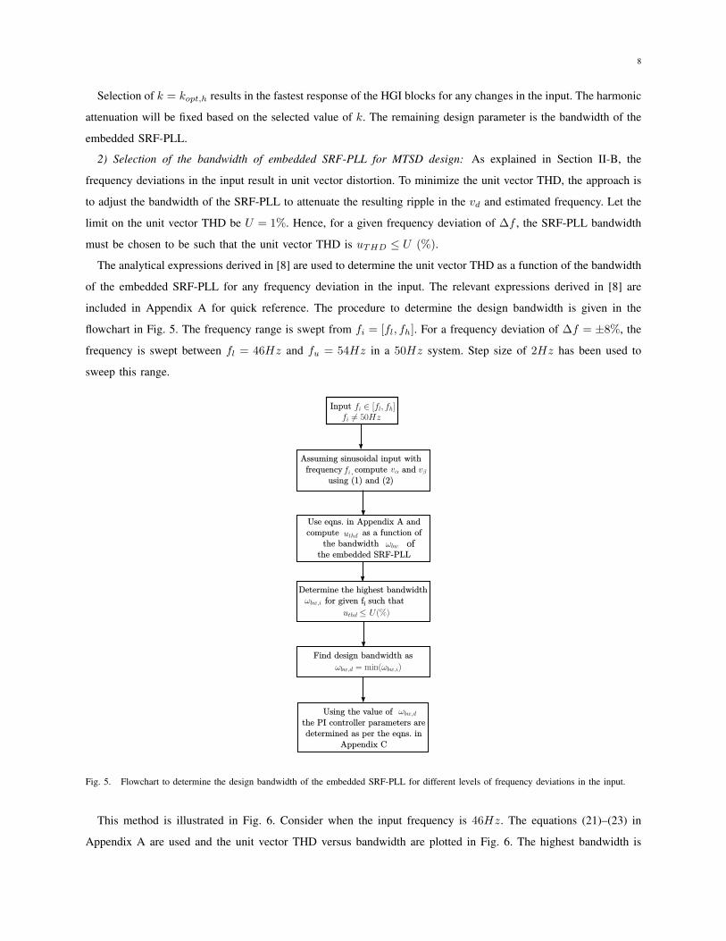
given by (30)–(32) in Appendix B. The resulting variation between the unit vector THD and the input THD for the
MTSD design of the HGI-PLL is given in Fig. 7.
Fig. 7. Variation of unit vector THD with input THD for upto ±8% frequency deviation in the input for MTSD design of HGI-PLL.
As it can be seen from Fig. 7, when the input has a THD of 5%, the unit vector THD is equal to 1.7% when the
input has frequency of 46Hz. Thus, when the input THD is assumed to be a worst-case value of 5% [29], [31], the
unit vector THD can exceed the 1% limit. To meet the objective of limiting the unit vector THD when the input
contains both frequency deviation and harmonics, an enhanced design procedure is evolved for the HGI-PLL. This
is termed as the HC-MTSD design. This design limits the unit vector THD to be within a limit of U = 1% and
achieves the fastest additive settling time while considering both frequency deviation and input THD. This design
method is explained in the following subsection.
B. HC-MTSD Design for HGI-PLL
The objectives of this design can be defined as follows.
minimize tsd = g(fbw, k) (11)
such that
uthd ≤ 1% (12)

11
given that the frequency deviation is ∆f(%) and the input THD is H(%).
The additive settling time tsd is a function of the HGI-PLL parameters fbw and k. This function is labelled
as g(fbw, k) in (11). Unit vector THD uthd is affected by both fbw and k. The upper limit on bandwidth for the
solution of (11) is considered to be 55Hz based on the MTSD design. This is because, from fundamental frequency
deviation point of view, any higher fbw would result in unit vector THD of higher than 1% as indicated in Fig. 6
for upto ±8% deviation in grid fundamental frequency. The lower limit is considered to be 20Hz. Theoretically,
the lower limit on the bandwidth can be close to zero.
The optimum solution for (11) considering the constraint (12) and the inputs of ∆f = ±8% and H = 5% is
determined within the bandwidth range of [fmin, fmax]. The range of k considered is [kmin, kmax]. These are
listed as follows.
fmin = 20Hz and fmax = 55Hz
kmin = 0.1 and kmax = 4 (13)
The range of k considers a wide possible design selection range as in Fig. 4. This range includes the kopt,h for the
MTSD design specified in (6).
The procedure for HC-MTSD design is explained using a flowchart in Fig. 8. This is qualitatively explained as
follows. For every bandwidth value in the range considered, the set of k satisfying unit vector THD to be less than
1% is determined. This set is designated as Ku in the flowchart in Fig. 8. In this set Ku, the value of k that gives
fastest response time for the HGI is determined. This is done using a procedure similar to the plot in Fig. 4. This
value of k is selected as the corresponding value to the bandwidth chosen. The additive settling time of of the
HGI-PLL is computed for this pair of bandwidth and k. This is repeated for a large number of bandwidth values
in the range specified in (13). For each bandwidth, a corresponding k and settling time are determined. The pair
with least additive settling time is selected as the design value based on the objective in (11).
The solution to this method is illustrated graphically as follows. The valid solution points contain three components
which are fbw,i, ki and corresponding tsd,i. In the top trace in Fig. 9, ki is plotted versus fbw,i. In the bottom trace,
tsd,i is plotted versus fbw,i. It can be observed that a minimum tsd is obtained for fbw = 29Hz in the bottom trace.
The corresponding k = 1.56. This is the optimal pair of fbw and k and gives a settling time of 37.9ms which is
less than two fundamental cycles in a 50Hz system. The plot in Fig. 9 is for a worst case input THD of H = 5%
and frequency deviation of ∆f = ±8%.
The variation of unit vector THD versus input THD and input frequency deviations is shown in Fig. 10 for the
HC-MTSD design. Fig. 10 can be compared with Fig. 7. It can be seen that with the HC-MTSD design, the unit
vector THD stays within 1% for the worst case condition of input THD of upto 5% with frequency deviation of
upto ±8%.

12
Input
Is for given maximum
input THD
Include
Find for this using Fig. 4
Update in the range till the range
is covered
Choose a corresponding to such that and
is the minimum
Store the dataset of andthe corresponding settling time
Update
Stop once sweepsthe range
Output the design pair with the minimum for the
full range of the index i
No
Yes
Initialize
Starting with
?
Fig. 8. Flowchart showing the steps in HC-MTSD design of HGI-PLL.
IV. DESIGN SUMMARY
In the proposed design methods, the parameter k and the bandwidth of the embedded SRF-PLL are selected.
These parameters are general and not system specific. This is because in the HGI, the transfer functions in (1) and
(2) are fixed. The sampling frequency and type of digital implementation determine the final difference equations.
However, the value of k will remain as per the proposed design in any system. Similarly, the SRF-PLL bandwidth
is a general parameter. The PI controller parameters, which are calculated using the bandwidth value using (33) –
(34), are system specific and their value will depend on discretization methods and sampling frequency. However,
the bandwidth value will remain as per the proposed designs. Hence, the overall design summary applies to any

13
t sd,i (
s)
0.030.040.050.060.070.080.09
Bandwidth of the embedded SRF-PLL (Hz)10 15 20 25 30 35 40 45 50 55
k i
0.5
1
1.5
2k=1.56
Min tsd=37.9ms
Fig. 9. HC-MTSD design for HGI-PLL. Variation of ki with bandwidth (top trace), and variation of additive settling time tsd,i with bandwidth
(bottom trace).
Fig. 10. Variation of unit vector THD with input THD for upto ±8% frequency deviation in the input for the proposed HC-MTSD design.
general single-phase system. It is given as follows.
1) Minimum tsd design (MTSD design): This design selects the HGI-PLL design parameters considering worst
case input frequency deviation and limit on unit vector THD. For these conditions, this design obtains the
fastest response. The design parameters determined for a frequency deviation of ±8% and unit vector THD
limit of 1% are:
k = 1.56, fbw = 55Hz, tsd = 27.6ms (14)
2) Harmonic constrained Minimum tsd design (HC-MTSD design): This design is an extension of the MTSD
design. It selects the HGI-PLL design parameters considering worst case input frequency deviation, worst
case input THD and a constraint on the unit vector THD. For these conditions, this design obtains the fastest
response. The design parameters determined for a frequency deviation of ±8%, input voltage THD of 5% with
the constraint of (10) and unit vector THD limit of 1% are:
k = 1.56, fbw = 29Hz, tsd = 37.9ms (15)
14
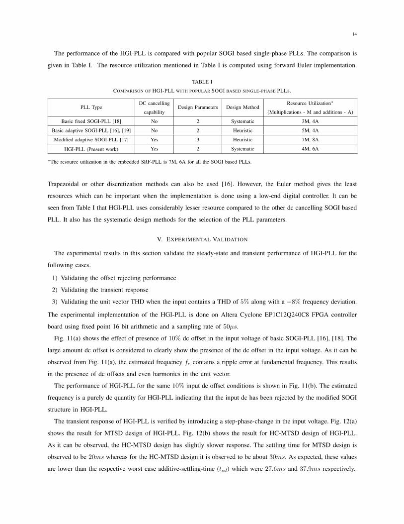
The performance of the HGI-PLL is compared with popular SOGI based single-phase PLLs. The comparison is
given in Table I. The resource utilization mentioned in Table I is computed using forward Euler implementation.
TABLE I
COMPARISON OF HGI-PLL WITH POPULAR SOGI BASED SINGLE-PHASE PLLS.
PLL TypeDC cancelling
capabilityDesign Parameters Design Method
Resource Utilization∗
(Multiplications - M and additions - A)
Basic fixed SOGI-PLL [18] No 2 Systematic 3M, 4A
Basic adaptive SOGI-PLL [16], [19] No 2 Heuristic 5M, 4A
Modified adaptive SOGI-PLL [17] Yes 3 Heuristic 7M, 8A
HGI-PLL (Present work) Yes 2 Systematic 4M, 6A
∗The resource utilization in the embedded SRF-PLL is 7M, 6A for all the SOGI based PLLs.
Trapezoidal or other discretization methods can also be used [16]. However, the Euler method gives the least
resources which can be important when the implementation is done using a low-end digital controller. It can be
seen from Table I that HGI-PLL uses considerably lesser resource compared to the other dc cancelling SOGI based
PLL. It also has the systematic design methods for the selection of the PLL parameters.
V. EXPERIMENTAL VALIDATION
The experimental results in this section validate the steady-state and transient performance of HGI-PLL for the
following cases.
1) Validating the offset rejecting performance
2) Validating the transient response
3) Validating the unit vector THD when the input contains a THD of 5% along with a −8% frequency deviation.
The experimental implementation of the HGI-PLL is done on Altera Cyclone EP1C12Q240C8 FPGA controller
board using fixed point 16 bit arithmetic and a sampling rate of 50µs.
Fig. 11(a) shows the effect of presence of 10% dc offset in the input voltage of basic SOGI-PLL [16], [18]. The
large amount dc offset is considered to clearly show the presence of the dc offset in the input voltage. As it can be
observed from Fig. 11(a), the estimated frequency fe contains a ripple error at fundamental frequency. This results
in the presence of dc offsets and even harmonics in the unit vector.
The performance of HGI-PLL for the same 10% input dc offset conditions is shown in Fig. 11(b). The estimated
frequency is a purely dc quantity for HGI-PLL indicating that the input dc has been rejected by the modified SOGI
structure in HGI-PLL.
The transient response of HGI-PLL is verified by introducing a step-phase-change in the input voltage. Fig. 12(a)
shows the result for MTSD design of HGI-PLL. Fig. 12(b) shows the result for HC-MTSD design of HGI-PLL.
As it can be observed, the HC-MTSD design has slightly slower response. The settling time for MTSD design is
observed to be 20ms whereas for the HC-MTSD design it is observed to be about 30ms. As expected, these values
are lower than the respective worst case additive-settling-time (tsd) which were 27.6ms and 37.9ms respectively.

15
uin_ph
vg
f e
4ms/div(a)
uin_ph
vg
f e
4ms/div(b)
Fig. 11. Effect of a 10% dc offset on (a) basic SOGI-PLL and (b) HGI-PLL. Ch. A = In-phase unit vector uin ph (1pu/div), Ch. B = Input
voltage vg (5V/div), Ch. C = Estimated frequency fe(50Hz/div).
En
uin_ph
vg
f e
10ms/div(a)
En
uin_ph
vg
f e
10ms/div(b)
Fig. 12. Transient response of HGI-PLL to step-phase-change in the input (a) MTSD design (b) HC-MTSD design. Ch. A = In-phase unit
vector uin ph (1pu/div), Ch. B = Input voltage vg (5V/div), Ch. C = Estimated frequency fe(50Hz/div), Ch. D = Enable (En) signal.

16
The effect of harmonics and frequency deviation in the input voltage is verified next. The input voltage has a
fundamental frequency of 46Hz which corresponds to a −8% frequency deviation. The input voltage also has a 5%
THD. The performance of HGI-PLL with MTSD design for this input voltage is shown in Fig. 13(a). The response
of HGI-PLL for the same input condition with HC-MTSD design is shown in Fig. 13(b).
uin_ph
vg
f e
4ms/div(a)
uin_ph
vg
f e
4ms/div(b)
Fig. 13. Effect of −8% frequency deviation in the input voltage with 5% THD on HGI-PLL for (a) MTSD design and (b) HC-MTSD design.
Ch. A = In-phase unit vector uin ph (1pu/div), Ch. B = Input voltage vg (5V/div), Ch. C = Estimated frequency fe (50Hz/div).
The time domain waveforms of the in-phase unit vector do not show significant difference in distortion. However,
spectrum of the unit vectors was obtained from the experimental waveforms. The unit vector THD corresponding
to the Fig. 13(a) and (b) is compared with the unit vector THD from analytical results and simulation result in
Table II(a) and (b). It can be observed that for the case of input fundamental frequency of 46Hz, the unit vector
THD is reduced to less than 1% when the HC-MTSD design is used. This table shows the detailed comparison
between analytical, simulation and experimental results when the input THD is 5% and frequency varies from 46Hz
to 54Hz with a ±8% deviation from the nominal 50Hz case. The comparison is done for both MTSD and HC-MTSD
designs. It can be observed that the values of THD are in agreement. The deviations observed in the experimental
result are attributed to the accuracy limitation of the oscilloscope in measuring the individual harmonics of low
amplitude and the quantization errors.
VI. CONCLUSION
In this paper, systematic designs are proposed for high-pass generalized integrator based PLL (HGI-PLL) for
single-phase grid-connected power converter application. This is a modified fixed-parameter SOGI-PLL with input

17
TABLE II
COMPARISON OF ANALYTICAL, SIMULATION AND EXPERIMENTALLY OBSERVED UNIT VECTOR THD OF HGI-PLL FOR (A) MTSD DESIGN
AND (B) HC-MTSD DESIGN. INPUT THD IS 5% WITH FUNDAMENTAL FREQUENCY VARIATION OF UPTO ±8%.
Fundamental Unit vector THD (%)
Frequency (Hz) Analytical Simulation Experimental
46 1.7 1.6 1.5
48 1.3 1.3 1.3
50 1.0 1.0 1.0
52 0.8 0.8 0.8
54 0.9 0.7 0.7
(a) MTSD design
Fundamental Unit vector THD (%)
Frequency (Hz) Analytical Simulation Experimental
46 1.0 0.9 0.9
48 0.8 0.7 0.8
50 0.6 0.6 0.5
52 0.5 0.4 0.4
54 0.5 0.4 0.4
(b) HC-MTSD design
dc offset rejection capability. This property of dc rejection is important as the basic SOGI-PLLs do not have this
capability and can result in dc injection to the grid when input contains dc offsets. The performance of HGI-PLL
is affected by the non-ideal input conditions of frequency deviations as well as harmonic distortions. These non-
idealities result in the harmonic distortion of the PLL unit vectors. This is undesirable as the unit vectors are used
for the reference generation in the closed-loop control of the grid-connected power converter.
Systematic design methods are proposed in this paper for the HGI-PLL. Firstly, the HGI-PLL parameters are
selected considering a worst case input frequency deviation. For a constraint on the unit vector THD of 1%, this
design achieves fastest response of the HGI-PLL. This method can exceed the limit on unit vector THD when the
input contains considerable harmonic distortion. Hence, to mitigate this problem, this design is evolved to include
the non-ideality of the input voltage harmonic distortion. This is an extension of the first design and it selects the
HGI-PLL parameters considering worst case frequency deviations as well as the THD in the input voltage. The
design parameters are selected such that for the given worst case conditions, the HGI-PLL has the fastest response
without exceeding the unit vector THD limit of 1%.
The proposed designs have been validated experimentally and are found to agree with the analysis. The HGI-PLL
uses considerably lesser resources while being able to provide good steady-state and transient performance. The
proposed design method can be extended to arbitrary single-phase systems. HGI-PLL with the proposed designs is
a suitable PLL scheme when low-end digital controllers are used in the control of grid-connected power converter

18
systems, as it has low implementation complexity.
APPENDIX A
QUANTIFYING THE EFFECT OF FREQUENCY DEVIATION ON UNIT VECTOR HARMONIC DISTORTION
When there is a frequency deviation in the input, the amplitudes of vα and vβ become unequal as can be seen
from the Bode plot in Fig. 3. Let these voltages be defined as follows.
vα = V1 sin(ωt+ φ1) (16)
vβ = V2 sin(ωt+ φ2) (17)
From the Bode plot in Fig. 3, it can be deduced that V1 6= V2 in (16) and (17). Similarly, φ1 6= φ2 and φ1−φ2 = π/2.
These parameters are known from the transfer functions of the HGI for any given input frequency.
Due to the unequal amplitudes, the two-phase equivalent voltages vα and vβ contain an unbalance and hence a
negative sequence component. This causes the well known problem of double fundamental frequency ripple in vd,
vq and estimated frequency ωe. As the estimated phase θe is integral of ωe, it will have the following form:
θe = ωet+ f (18)
In (18), f is a second harmonic ripple error. This is defined in (19) below. The aim is to determine the parameters
a and φ in the equation shown below,
f = a sin(2ωt+ φ) (19)
In (19), ω is the fundamental frequency whose nominal value is ω = ω0 = 2π50 rad/s. It is assumed that the
fundamental frequency can vary upto ±8% in this paper. For given f , it is shown in [8] that the unit vector will
have a third harmonic amplitude equal to
u3 =a
2(20)
The detailed derivation steps to determine a and φ are provided in [8]. Only the final expressions are reproduced
here:
a =m[(V1/2) cos(φ1 + x) + (V2/2) sin(φ2 + x)]
cos(φ)−m cos(φ+ x)[− cos(φ1)V1/2 + sin(φ2)V2/2]
φ = arctan
[α+ βν
αν − β
]− x (21)
Where
α = cos(x) + [(V1/2) cos(φ1)− (V2/2) sin(φ2)]m
β = sin(x)
ν =(V1/2) cos(φ1 + x) + (V2/2) sin(φ2 + x)
(V1/2) sin(φ1 + x)− (V2/2) cos(φ2 + x)(22)

19
In (21) and (22), m and x are the the overall magnitude gain and phase shift at second harmonic frequency given
by the summer, PI controller and integrator in the embedded SRF-PLL in Fig. 2. They are expressed as follows:
m =
∣∣∣∣∣−(kp +
kis
)1
s
∣∣∣∣∣s=j2ω
x = 6(−(kp +
kis
)1
s
)∣∣∣∣∣s=j2ω
(23)
Thus, for a given frequency deviation, the output of the HGI vα and vβ can be determined. Then the above
equations can be used to determine a which equals to twice the amplitude of the third harmonic in the unit
vector [8].
B QUANTIFYING THE EFFECT OF GRID VOLTAGE HARMONICS ON UNIT VECTOR HARMONIC DISTORTION
Let the sensed grid voltage contain a harmonic of the order h. Depending on the transfer functions of the HGI,
the voltages vα and vβ will also contain harmonic of the order h whose magnitude and phase can be calculated.
Let these harmonic voltages be defined in phasor form as follows:
vhα = Vhα 6 φh
vhβ = Vhβ 6 ψh (24)
The phasors in (24) rotate at the harmonic frequency that is h times the fundamental. These harmonic voltages can
be split into positive and negative sequence voltages in two-phase system as follows:
vhαp =vhα + jvhβ
2
vhαn =vhα − jvhβ
2(25)
In (25), the voltages vhαp and vhαn are the α axis positive and negative sequence voltages. The corresponding β
axis voltages are given by,
vhβp = −jvhαp
vhβn = jvhαn (26)
The expressions in (26) are obtained based on the fact that β axis voltage lags α axis voltage by 90◦ in positive
sequence while it leads by 90◦ in negative sequence. By adding up positive and negative sequence voltages, the
original voltages in (24) can be obtained.
In [8], unit vector harmonic distortion is determined analytically when the input contains a harmonic of any
given sequence. The harmonic with order h occurring as a positive sequence gives rise to (h − 2) and h order
harmonics in the unit vectors. Similarly the harmonic with order h occurring as a negative sequence gives rise to
h and (h+ 2) order harmonics in the unit vectors.

20
The expressions in [8] are reproduced here for computing the distortion due to positive sequence harmonic. Let
these voltages be:
vhαp = Vh sin(hωt+ γ)
vhβp = −Vh cos(hωt+ γ) (27)
The expressions in (27) are the general time domain expressions of the corresponding phasors specified in (25) and
(26). The sensed grid voltage has a positive sequence fundamental voltage given in the following general form:
v1+(α) =V1+ sin(ωt+ δ)
v1+(β) =− V1+ cos(ωt+ δ) (28)
For the input conditions as in (28) and (27), the analytical expressions are derived in [8] to compute the (h − 2)
and h order harmonics in the unit vector. The sine unit vector will have the following form for these harmonics,
uh−2 =ah sin((h− 2)ωt+ φh)
uh =ah sin(hωt+ φh) (29)
The final expressions for the amplitude and phase in (29) are as follows.
φh = arctan
[αh − βh cot(xh−1 + γ)
βh + αh cot(xh−1 + γ)
]ah =
0.5Vhmh−1 cos(xh−1 + γ)
cos(φh) +mh−1V1+ cos(δ) cos(φh + xh−1)(30)
Where
αh = 1 +mh−1V1+ cos(δ) cos(xh−1)
βh = mh−1V1+ cos(δ) sin(xh−1) (31)
In (30) and (31), mh−1 and xh−1 are the the overall magnitude gain and phase shift at second harmonic frequency
given by the summer, PI controller and integrator in the embedded SRF-PLL in Fig. 2. They are expressed as follows:
mh−1 =
∣∣∣∣∣−(kp +
kis
)1
s
∣∣∣∣∣s=j(h−1)ω
xh−1 = 6(−(kp +
kis
)1
s
)∣∣∣∣∣s=j(h−1)ω
(32)
For the negative sequence harmonic, the same expressions (30)–(32) can be used by replacing h − 1 with h + 1.
The overall THD is determined by performing a phasor sum of the harmonics in the unit vector appearing due to
all the positive sequence and negative sequence harmonics in the input voltage to the embedded SRF-PLL.

21
C EXPRESSIONS FOR THE PI CONTROLLER PARAMETERS
For any given design bandwidth of the embedded SRF-PLL (ωbw), the PI controller parameters kp and ki can
be determined uniquely. The corresponding equations are as follows [12], [21],
kp =ωbwVm
(33)
ki = kpTsω2bw (34)
In (34), parameter Ts is the sampling time used in the digital implementation of the SRF-PLL. In (33), Vm is the
nominal sensed grid voltage peak.
REFERENCES
[1] K. Nagaraj, A. S. Kamath, K. Subburaj, B. Chattopadhyay, G. Nayak, S. S. Evani, N. P. Nayak, I. Prathapan, F. Zhang, and B. Haroun,
“Architectures and circuit techniques for multi-purpose digital phase lock loops,” IEEE Transactions on Circuits and Systems I: Regular
Papers, vol. 60, pp. 517–528, March 2013.
[2] H. Tao, J. Duarte, and M. Hendrix, “Control of grid-interactive inverters as used in small distributed generators,” in 42nd IAS Annual
Meeting, Industry Applications Conference, pp. 1574–1581, Sept 2007.
[3] Z. Wang, S. Fan, Y. Zheng, and M. Cheng, “Control of a six-switch inverter based single-phase grid-connected pv generation system with
inverse park transform pll,” in IEEE International Symposium on Industrial Electronics (ISIE), pp. 258–263, May 2012.
[4] R. Teodorescu and F. Blaabjerg, “Flexible control of small wind turbines with grid failure detection operating in stand-alone and grid-
connected mode,” IEEE Transactions on Power Electronics, vol. 19, pp. 1323–1332, Sept 2004.
[5] R. Menzies and G. Mazur, “Advances in the determination of control parameters for static compensators,” IEEE Transactions on Power
Delivery, vol. 4, pp. 2012–2017, Oct 1989.
[6] A. Norouzi and A. Sharaf, “Two control schemes to enhance the dynamic performance of the STATCOM and SSSC,” IEEE Transactions
on Power Delivery, vol. 20, pp. 435–442, Jan 2005.
[7] B. Singh and S. Arya, “Implementation of single-phase enhanced phase-locked loop-based control algorithm for three-phase dstatcom,”
IEEE Transactions on Power Delivery, vol. 28, pp. 1516–1524, July 2013.
[8] A. Kulkarni and V. John, “Analysis of bandwidth-unit-vector-distortion tradeoff in pll during abnormal grid conditions,” IEEE Transactions
on Industrial Electronics, vol. 60, pp. 5820–5829, Dec 2013.
[9] A. Luna, J. Rocabert, J. Candela, J. Hermoso, R. Teodorescu, F. Blaabjerg, and P. Rodriguez, “Grid voltage synchronization for distributed
generation systems under grid fault conditions,” IEEE Transactions on Industry Applications, vol. 51, pp. 3414–3425, July 2015.
[10] M. Karimi-Ghartemani, “A novel three-phase magnitude-phase-locked loop system,” IEEE Transactions on Circuits and Systems I: Regular
Papers, vol. 53, pp. 1792–1802, Aug 2006.
[11] C. Fitzer, M. Barnes, and P. Green, “Voltage sag detection technique for a dynamic voltage restorer,” IEEE Transactions on Industry
Applications, vol. 40, pp. 203–212, Jan 2004.
[12] V. Kaura and V. Blasko, “Operation of a phase locked loop system under distorted utility conditions,” IEEE Transactions on Industry
Applications, vol. 33, pp. 58–63, Jan 1997.
[13] Y. F. Wang and Y. W. Li, “Grid synchronization pll based on cascaded delayed signal cancellation,” IEEE Transactions on Power Electronics,
vol. 26, pp. 1987–1997, July 2011.
[14] M. Meral, “Improved phase-locked loop for robust and fast tracking of three phases under unbalanced electric grid conditions,” IET
Generation, Transmission Distribution, vol. 6, pp. 152–160, February 2012.
[15] A. Ghoshal and V. John, “Performance evaluation of three phase SRF-PLL and MAF-SRF-PLL,” Turkish Journal of Electrical Engineering
and Computer Sciences, vol. 23, pp. 1781–1804, 2015.
[16] M. Ciobotaru, R. Teodorescu, and F. Blaabjerg, “A new single-phase pll structure based on second order generalized integrator,” in 37th
IEEE Power Electronics Specialists Conference (PESC), pp. 1–6, June 2006.

22
[17] M. Ciobotaru, R. Teodorescu, and V. Agelidis, “Offset rejection for pll based synchronization in grid-connected converters,” in Twenty-Third
Annual IEEE Applied Power Electronics Conference and Exposition (APEC), pp. 1611–1617, Feb 2008.
[18] A. Kulkarni and V. John, “A novel design method for sogi-pll for minimum settling time and low unit vector distortion,” in 39th Annual
Conference of the IEEE Industrial Electronics Society-IECON 2013, pp. 274–279, Nov 2013.
[19] Y. Yang and F. Blaabjerg, “Synchronization in single-phase grid-connected photovoltaic systems under grid faults,” in 3rd IEEE International
Symposium on Power Electronics for Distributed Generation Systems (PEDG), pp. 476–482, June 2012.
[20] P. Rodriguez, R. Teodorescu, I. Candela, A. Timbus, M. Liserre, and F. Blaabjerg, “New positive-sequence voltage detector for grid
synchronization of power converters under faulty grid conditions,” in 37th IEEE Power Electronics Specialists Conference (PESC), pp. 1–
7, June 2006.
[21] A. Kulkarni and V. John, “Design of synchronous reference frame phase-locked loop with the presence of dc offsets in the input voltage,”
IET Power Electronics, vol. 8, no. 12, pp. 2435–2443, 2015.
[22] G. Buticchi, E. Lorenzani, and G. Franceschini, “A dc offset current compensation strategy in transformerless grid-connected power
converters,” IEEE Transactions on Power Delivery, vol. 26, pp. 2743–2751, Oct 2011.
[23] “IEEE standard for interconnecting distributed resources with electric power systems,” IEEE Std 1547-2003, 2003.
[24] J. Matas, M. Castilla, J. Miret, L. Garcia de Vicuna, and R. Guzman, “An adaptive prefiltering method to improve the speed/accuracy
tradeoff of voltage sequence detection methods under adverse grid conditions,” IEEE Transactions on Industrial Electronics, vol. 61,
pp. 2139–2151, May 2014.
[25] S. Shinnaka, “A robust single-phase pll system with stable and fast tracking,” IEEE Transactions on Industry Applications, vol. 44,
pp. 624–633, March 2008.
[26] M. Reza, M. Ciobotaru, and V. Agelidis, “Accurate estimation of single-phase grid voltage parameters under distorted conditions,” IEEE
Transactions on Power Delivery, vol. 29, pp. 1138–1146, June 2014.
[27] A. Timbus, M. Liserre, R. Teodorescu, P. Rodriguez, and F. Blaabjerg, “Evaluation of current controllers for distributed power generation
systems,” IEEE Transactions on Power Electronics, vol. 24, pp. 654–664, March 2009.
[28] X. Zong, P. Gray, and P. Lehn, “New metric recommended for IEEE Std. 1547 to limit harmonics injected into distorted grids,” IEEE
Transactions on Power Delivery, vol. PP, no. 99, pp. 1–1, 2015.
[29] “IEEE recommended practices and requirements for harmonic control in electrical power systems,” IEEE Std 519-1992, pp. 1–112, April
1993.
[30] K. Ogata, Modern Control Engineering. Prentice Hall, 5th ed., 2008.
[31] “IEEE recommended practice for monitoring electric power quality,” IEEE Std 1159-2009 (Revision of IEEE Std 1159-1995), pp. c1–81,
June 2009.