Embed Size (px)
Citation preview

1
Design of a Mixed-Signal Feedback Damper System
Michael J. Schulte
* Some slides are provided by Craig Deibele (Oak Ridge National Laboratory) and Anil Polisetti (UW-Madison)

2
Project Group• University of Wisconsin, Madison
– Michael Schulte– Anil Polisetti– Suman Mamidi– Zaipeng Xie
• Oak Ridge National Laboratory– Craig Deibele– Saeed Assadi– Jeffrey Patterson
• Los Alamos National Laboratory– Rob McCrady– Bob Macek
• Hardware components from Sundance DSP Inc.

3
Outline
• Project Goals and Motivation• System Overview• System Components
– Analog-to-digital and digital-to-analog converters– Field programmable gate array (FPGA) modules
• System Features• System Status• Future Work and Conclusions

4
Project Goals and Motivation
• Goal: Develop a mixed-signal feedback damper system for use at Oakridge and Los Alamos
• Provides– Flexibility in setting system parameters– Programmability to meet the needs of different
experiments– Improved data collection and analysis– Ability to correct for dispersion

5
Instability at SNS
Frequency spectrum of beam at Spallation Neutron Source

6
kickerpickup
Analog Feedback Damper System
• Replace portions of the analog system by digital hardware
• Add new functionality and capabilities

7
Mixed-Signal Damper System
• The new system combines analog and digital components
• The digital components are clocked at a multiple of the ring frequency (≈ 1 MHz)
Pickup Top
Pickup Bottom
Power Amplifier 1
Power Amplifier 2
Low-Pass Filter
ADCFPGA
Subsystem2-channel
DAC
System Clock Source
Kicker Top
Kicker Bottom
Analog Hybrid

9
Digital Subsystem Implementation
• The digital subsystem includes synchronized ADCs, FPGAs, and DACs• Desired operating frequency of roughly 400 MHz• Multiply ring frequency by a factor of about 400 to obtain the system
clock
Low-Pass Filter
SMT 384 Quad Channel
125 MSPS 14-bit ADC 1
SMT 368 with Virtex 4 FPGA
and 8MB SRAM
SMT 350Dual-Channel
500 MSPS 16-bit DAC
Power Amplifier 2
Data Processing
Power Amplifier 1
System Clock
Data Interleaving and Storage
SMT 398 with Virtex 2-ProFPGA and 16MB SRAM
10
Analog-to-Digital Converter• SMT384 ADC Module
– Quad-channel, 125 MSPS, 14-bit ADC– Data interleaving on FPGA provides a 500 MSPS, 14-bit data stream
* Figure from Sundance DSP, Inc.

11
Data Interleaving and Storage FPGA• SMT 398 FPGA Modules
– Contains Xilinx Virtex-II Pro FPGA – Interleaves data from ADCs for further processing– Stores up to 8 million 16-bit samples
* Figure from Sundance DSP, Inc.

12
Data Processing FPGA• SMT 368 FPGA Module
– Contains Virtex-4 FPGA– Stores up to 4 million 16-bit samples– Processes digital data and sends outputs to DAC
* Figure from Sundance DSP, Inc.

13
Digital-to-Analog Converter• SMT 350 DAC Module
– SMT350 Dual-Channel 500 MSPS, 16-bit DAC – Accepts data at 125 MSPS and interpolates by 4– Later upgrade to a true 500 MSPS, 14-bit DAC– Outputs sent to power amplifiers
* Figure from Sundance DSP, Inc.

14
Data Processing FPGA
• The FPGA contains high-speed DSP modules• Each module is programmable and can be bypassed• Input from the ADC and outputs to the DACs are
stored in high-speed memory
Programmable Delay Module
Comb Filter 1
FIR Filter 1
FIR Filter 2
Comb Filter 2
DAC 2
VoltageDifferenceFrom ADC
Inverter
DAC1
Gain Multiplier

15
Programmable Delay Module
• Phase between the pickup and kicker must be maintained between -90 and +90 degrees
• Programmable delay module controls the overall system delay: • FIFO length can be varied• Additional fine-tuning of the delay is required
periodClocklengthFIFODelay
Gain Multiplier Output (Vout)
Comb Filter 1 Input
Programmable Delay Module
WriteAddress
ReadAddress
Clock
FIFOLength
Programmable FIFO

16
Comb Filters
• The comb filters dampen the ring frequency harmonics to save power – Comb filter output: – Comb filter frequency response:
– tn is set as a multiple of the ring frequency (≈ 1 sec)
][][][ ntnxnxny ]1)[()( ntieXY
Splitter
Programmable Delay (tn)
Comb Filter Input (x[n])
Subtractor
x[n] x[n-tn]
x[n]
Comb Filter Output (y[n])
x[n]

17
Comb Filters
• The ring frequency harmonics occur at multiples of roughly 1 MHz• To dampen these harmonics, the clock for the comb filter must be synchronized to the
ring frequency
Frequency response of a comb filter locked to 1 MHz
0
0.5
1
1.5
2
2.5
0 2 4 6 8 10 12
Frequency(MHz)
Y(w
)
]1)[()( ntieXY

18
FIR Filters
• The FIR filters compute: • Serve as equalizers that correct for dispersion in analog components
– Cables have non-uniform magnitude and phase versus frequency– Amplifiers have phase dispersion– Analog hybrids and low-pass filters have magnitude and phase dispersion
b 1
yF IR [n ]
x [n ] z -1
xb 0
z -1
x
+
x
+
b 2
z -1
x
+
b M
x[n-M ]x [n -1 ] x [n -2 ]
F ilte r taps
][][0
knxbnyM
k k

19
Cable Magnitude Dispersion• The cables have magnitude and phase
dispersion due to copper and dielectric losses
Absolute value of S21 vs. frequency
-25
-20
-15
-10
-5
0
0 100000000 200000000 300000000 400000000 500000000 600000000
frequency
20 l
og
(S
21)
21S characteristics of the measurement cable (in dB) vs. frequency

20
Cable Phase Dispersion• The cables have magnitude and phase
dispersion due to copper and dielectric lossesPhase of Ideal Cable vs. Actual cable
-120
-100
-80
-60
-40
-20
0
0.0000E+00 1.0000E+08 2.0000E+08 3.0000E+08 4.0000E+08 5.0000E+08 6.0000E+08
frequency( Hz )
Ph
ase (
Deg
rees)
Ideal cable
Actual cable
Phase response of Ideal cable vs. Actual cable

21
Cable Dispersion• Cable magnitude and phase dispersion is seen
in its time domain responseTime-domain response of Ideal cable vs. Actual cable
-10000000
0
10000000
20000000
30000000
40000000
50000000
60000000
70000000
-4.00E+01 -2.00E+01 0.00E+00 2.00E+01 4.00E+01 6.00E+01 8.00E+01
Time(ns)
Mag
nit
ud
e
Ideal Cable
Actual cable
Time-domain response of Ideal cable vs. Actual cable

22
Reducing Cable Dispersion• Find the frequency (S21) characteristics of the cable
using a vector network analyzer• Determine the equalizer characteristics that compensate
for the cables magnitude and phase dispersion
Phase of Ideal cable , Actual cable and Equalizer
-150
-100
-50
0
50
100
150
0.0000E+00 1.0000E+08 2.0000E+08 3.0000E+08 4.0000E+08 5.0000E+08 6.0000E+08
Frequency(Hz)
Ph
ase (
Deg
rees) Ideal Cable
Actual cable
Equalizer
Phase response of idea cable, actual cable and the equalizer versus frequency
dTieS
HG
*)(
2)(
21
c
H2
cos2 4
23
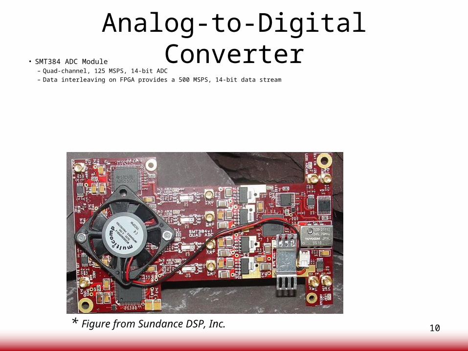
Reducing Cable Dispersion• Determine the number of taps and tap values for the
equalizer• Run the equalizer in series with the cable to reduce
dispersion
Comparison of cable responses
-0.2
0
0.2
0.4
0.6
0.8
1
1.2
-40 -20 0 20 40 60 80 100
Time(ns)
No
rmal
ized
ou
tpu
t
Ideal Cable response
Actual Cable response
De-embedded cable response
Comparison of the time-domain responses of an ideal, actual, and de-embedded cable

24
Reducing Overall Dispersion• The impact of other sources of dispersion in the system
can be reduced using similar techniques• FIR filters can be designed to compensate for multiple
dispersion sources:
Phase spectrum of an anti-aliasing LPF with cut-off frequency 180 MHz
-150
-100
-50
0
50
100
150
200
0 100 200 300 400 500 600
Frequency(MHz)
Ph
ase(
deg
rees)
Phase spectrum of anti-aliasing LPF with cut-off frequency of 180 MHz
dTieLPFS
HG
*)(*)(
2)(
21

25
System Status• Digital subsystem (ADCs, FPGAs, DACs) currently under construction by Sundance DSP• Preliminary FPGA subsystem design
– Modeled, synthesized, and initial testing
– Correct operation of digital components
– Operating frequency of roughly 400 MHZ
– Simulation model developed using Matlab and DSP System Generator
• Technique for compensating for dispersion– Developed for cables
– In-progress for other analog components

26
Future Work• Design and test the FPGA control to set system
parameters and filter coefficients• Develop a GUI to enter parameters and filter coefficient • Use the Matlab simulation model and experimental data
to refine the design • Test complete digital subsystem (first without and then
with the ADCs and DACs)• Test complete system at ORNL• Improve the design based on experimental results• Automate the system for adaptive processing
– Hardware/software adjustment of parameter values

27
Conclusions• The mixed-signal feedback damper system has
important benefits– Added flexibility and programmability– Improved data collection and analysis– Reduce dispersion from analog components
• It also has significant challenges– Achieving high clock rate on ADCs, FPGAs, and DACs– Generating clocks synchronized to the ring frequency– System integration and testing
• Preliminary results look promising and the system has the potential for future upgrades

28
Backup Slides

29
Mixed-Signal Damper SystemPickup
Top
Pickup Bottom
PowerAmplifier 1
PowerAmplifier 2
Low-PassFilter 1
ADC 1
FPGASubsystem
2-ChannelDAC
System Clock Source
Kicker Top
Kicker Bottom
Low-PassFilter 2
ADC 2
• The new system combines analog and digital components
• The digital components are clocked at a multiple of the ring frequency

30
Digital Subsystem Implementation
• The digital subsystem includes synchronized ADCs, FPGAs, and DACs
Low-Pass Filter 2
SMT 384 Quad Channel
125 MSPS 14-bit ADC 1
SMT 398 with Virtex 2-ProFPGA and 16MB SRAM
SMT 384 Quad Channel
125 MSPS 14-bit ADC 2
SMT 368 with Virtex 4 FPGA
and 8MB SRAM
SMT 350Dual-Channel
500 MSPS 16-bit DAC
Power Amplifier 2
Data Interleaving and Storage
Low-Pass Filter 1
Data Processing
Power Amplifier 1System
Clock
Data Interleaving and Storage
SMT 398 with Virtex 2-ProFPGA and 16MB SRAM

31
Offset and Gain Multipliers
• Offset multipliers correct the closed orbit offset– Set M1 and M2, such that
is close to zero when the beam is stable
• Subtractor provides scaled voltage difference• Gain multiplier controls overall system gain• Implemented using high-speed DSP48 modules
Subtractor
V2
(ADC 2)
V1
(ADC 1)
Offset Multiplier 2
(M2)
Offset Multiplier 1
(M1) Gain
Multiplier (G)
Vout
V1*M1
V2*M2
V1
V2
)( 2211 MVMVGVout

32
Data Processing FPGA
• The FPGA contains high-speed DSP modules• Each module is programmable and can be bypassed• Input from the ADCs and outputs to the DACs are
stored in high-speed memory
Programmable Delay Module
Comb Filter 1
FIR Filter 1
FIR Filter 2
SubtractorComb Filter 2
DAC 2ADC 2
ADC 1
Inverter
DAC1
Offset Multiplier 2
Offset Multiplier 1
Gain Multiplier

33
Alternative Mixed Signal System
Pickup Top
Pickup Bottom
Power Amplifier 1
Power Amplifier 2
Low-Pass Filter
ADCFPGA
Subsystem2-channel
DAC
System Clock Source
Kicker Top
Kicker Bottom
Analog Hybrid
• The offset multipliers and subtraction can be implemented using analog circuits
+ Reduces system complexity
+ May improve accuracy of voltage difference– Introduces additional distortion from analog components– Reduces available diagnostic information

34
Digital Subsystem Implementation
• Implementing the offset multipliers and subtraction using analog circuits + Eliminates one of the ADCs and one of the FPGAs modules– Reduces available diagnostic information, since individual voltages are no
longer available
Low-Pass Filter
SMT 384 Quad Channel
125 MSPS 14-bit ADC 1
SMT 368 with Virtex 4 FPGA
and 8MB SRAM
SMT 350Dual-Channel
500 MSPS 16-bit DAC
Power Amplifier 2
Data Processing
Power Amplifier 1
System Clock
Data Interleaving and Storage
SMT 398 with Virtex 2-ProFPGA and 16MB SRAM

35
Digital Subsystem
• The digital subsystem includes synchronized ADC, FPGA, and DAC modules

36
External Clock Source
• The external clock source is synchronized to a multiple of ring frequency.
• For SNS, this is obtained by a multiple of 450.– Ring frequency of SNS 1MHz (approx)– Required clock is 450 MHz (approx)

37
External Clock Source
• Locking the clock is crucial for correct operation– Very important to maintain phase difference between
pickup and kicker – Range of phase difference for proper operation of
system from -90 to +90 degrees– Phase difference controlled through programmable
delay module

38
External Clock Source
• Frequency response of a Comb Filter properly locked to 1MHz
Frequency response of a comb filter locked to 1 MHz
0
0.5
1
1.5
2
2.5
0 2 4 6 8 10 12
Frequency(MHz)
Y(w
)

39
External Clock Source
• Frequency response of the same comb filter with an error of 50KHz in the original clock– Leads to an error of 22.5 MHz in the clock to the FPGA.
Frequency response of a comb filter not locked to 1 MHz
0
0.5
1
1.5
2
2.5
0 2 4 6 8 10 12
Frequency(MHz)
Y(w
)

40
External Clock Source contd.
• Comparison of comb filter outputs.
Frequency response of a locked comb filter vs. comb filter not locked
0
0.5
1
1.5
2
2.5
0 2 4 6 8 10 12
Frequency(MHz)
Y(w
)
Comb filter locked to 1 MHz
Comb filter not locked to1MHz

41
Programmable delay
• Phase difference between Pickup and Kicker between -90 and 90 to maintain negative feedback.
• Any change in this phase difference can lead to driving the instabilities instead of damping them.
• This phase difference is obtained by varying the delay values.

42
Comb Filters
• Structure of a Comb Filter
,td is a constant, here 1µsec
• Used to save power for stable fixed beam offsets
S e i t d2 1
1
21

43
Comb Filter contd.• Need for the Comb Filter
Fourier Spectrum of the beam
• Major part of spectral power due to ring harmonics.• Notching out ring harmonics will not affect the instabilities.
44
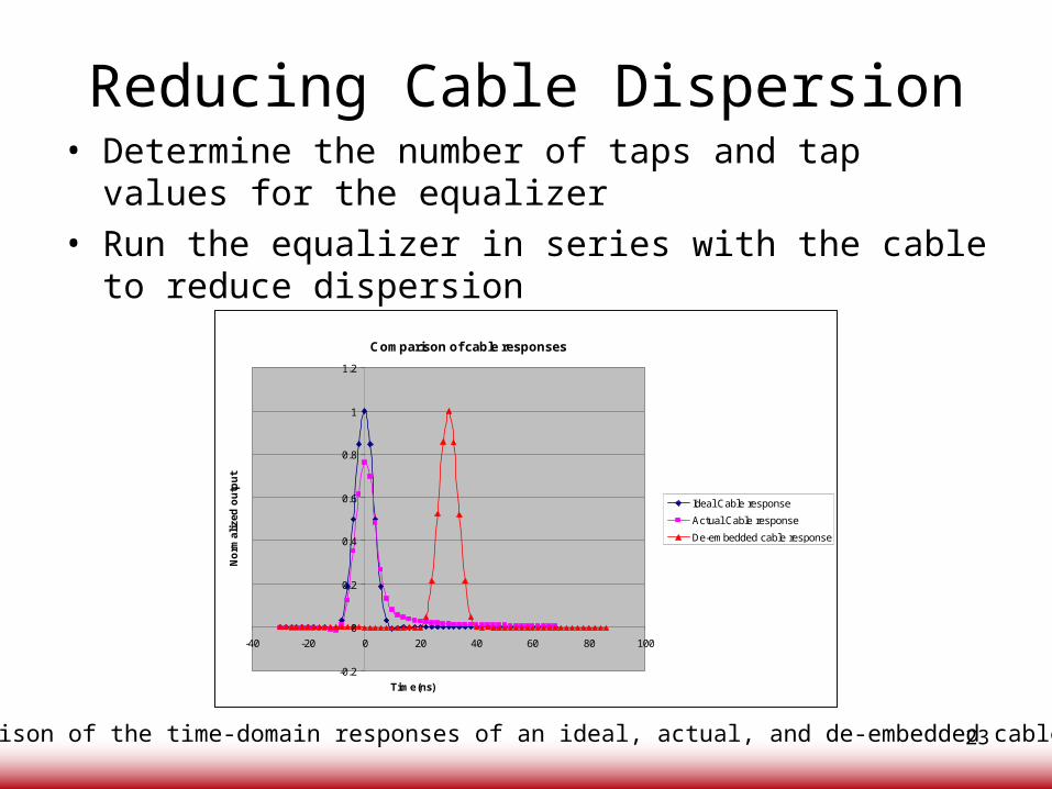
Comb Filter contd.
• Transmission characteristics
0 1 107 2 107 3 107 4 107 5 107100
50
0
S21 (dB)
Transmission of Comb Filter
Frequency (Hz)
Tra
nsm
issi
on (
dB
)
4.822 10 15
100
20 log s21j
5 1071 fj

![ACATacat.or.th/download/acat_or_th/journal-4/04 - 04.pdf · APmin APmax Appendix G [1] AP APmax Overpressure Relief Damper Damper 12 Relief Damper Relief Damper (Vent) Fire Damper](https://img.pdfslide.net/doc/110x75/5f7cb481641db55595223717/-04pdf-apmin-apmax-appendix-g-1-ap-apmax-overpressure-relief-damper-damper.jpg)