Embed Size (px)
Citation preview

MLX90291 Datasheet
REVISION 5 - NOVEMBER 2, 2016
390109029101
1. Features and Benefits
Programmable Hall effect sensor
12-bit 125Hz PWM output signal proportional to the magnetic flux density
Switch function
Measurement range from ±15mT to ±400mT
Low noise output signal (PWM jitter)
Programmable through the connector (supply, ground & output)
16 bit customer ID number (48 bit MLX ID for traceability purposes)
SOIC8 package RoHS compliant
Lead free component, suitable for lead free soldering profile 260°C
2. Application Examples
Rotary position sensor
Linear position sensor
Contactless switch
Figure 1
3. Description
The MLX90291 is a monolithic programmable linear hall sensor IC, which can provide a PWM output signal proportional to the externally applied magnetic flux density or act as a switch with a programmable threshold level. The transfer characteristic of the MLX90291 is fully programmable (offset, gain, clamping levels …).
Hall Bias
Integrating P2P
DIDO
4-Phase Switch
Box
fs = 1MHz
Oscillator1 MHz
Clock Generator
I = 4 x 0.35mAS = 80mV/TVh= 4mV @50mT
G = 15 … 190G = 4
fs = 1MHz
Input data rate
Voltage Regulator
DIGITAL + EEPROM
FG[1
2:0
]
FILT
CO
DE[
3:0
]RG[2:0] ATTN2P5
CLA
MP
[2:0
]
3.3V core
TC1ST[6:0]
TC2ND[5:0]
XA
[13
:0]
ADC
PWM Logic
Test Controller
TEST1
TEST2
TEST3
VDD
VSS
3.3V ana
3.3V dig
fc = 1MHz
digital clock
f = 15kHz
data conversion
rate
Control lines
SLO
PE
LIM
ITER
OU
TSLO
PE[
1:0
]
OUTPUT
Program.Attenuation
by 1 or 4.5
TEST5
OUT
YA[1
4:0
]
TEST4
Reverse Polarity
Protection

MLX90291 SMD Programmable Linear Hall Sensor IC Featuring PWM Output
Page 2 of 22
REVISION 5 - NOVEMBER 2, 2016
3901090291
Contents
1. Features and Benefits ............................................................................................................................ 1
2. Application Examples ............................................................................................................................. 1
3. Description ............................................................................................................................................ 1
4. Ordering Information ............................................................................................................................ 4
5. Glossary of Terms .................................................................................................................................. 4
6. Pin Definitions and Descriptions ............................................................................................................ 5
6.1. Absolute Maximum Ratings ............................................................................................................... 5
7. General Electrical Specifications ............................................................................................................ 6
8. Magnetic Specification .......................................................................................................................... 7
9. Timing Specification............................................................................................................................... 7
10. PWM output specification ................................................................................................................... 9
11. Fault Modes....................................................................................................................................... 10
12. Programmable Items ......................................................................................................................... 11
12.1. Parameter Table ............................................................................................................................. 11
12.2. Output mode configuration (OUTMODE)...................................................................................... 11
12.3. Sensitivity programming (ROUGHGAIN, FINEGAIN) ..................................................................... 12
12.4. Offset / output quiescent voltage programming (XA, YA) ............................................................ 13
12.5. Clamping level programming (CLAMP) .......................................................................................... 13
12.6. Bandwidth and filter programming (FILTCODE) ............................................................................ 14
12.7. Current limitation (OUTSLOPE) ...................................................................................................... 14
12.8. PWM Mode duty cycle definition (DCDEF) ................................................................................... 14
12.9. Sensitivity and temperature drift programming (TC1ST, TC2ND) ................................................ 15
12.10. Offset temperature drift programming (OFFDRIFT) ................................................................... 16
12.11. Functional Mode (SWITCH) .......................................................................................................... 17
12.12. Polarity (PLATEPOL) ...................................................................................................................... 17
12.13. Attenuator (ATTN2P5) .................................................................................................................. 17
12.14. Customer ID (CSTID) ..................................................................................................................... 17
13. Recommended Application Diagrams ................................................................................................ 17
13.1. Resistor and Capacitor Values ........................................................................................................ 17
13.2. Pull down resistor for diagnostic low ............................................................................................ 18
13.3. Pull up resistor for diagnostic high ................................................................................................ 18

MLX90291 SMD Programmable Linear Hall Sensor IC Featuring PWM Output
Page 3 of 22
REVISION 5 - NOVEMBER 2, 2016
3901090291
14. Package Information .......................................................................................................................... 18
14.1. SOIC8 Package Dimensions ............................................................................................................ 19
14.2. SOIC8 Pin Out and Marking ............................................................................................................ 19
14.3. SOIC8 Hall plate positioning ........................................................................................................... 20
15. Standard Information ........................................................................................................................ 21
16. ESD Precautions ................................................................................................................................. 21
17. Revision History Table ....................................................................................................................... 21
18. Contact .............................................................................................................................................. 21
19. Disclaimer .......................................................................................................................................... 22

MLX90291 SMD Programmable Linear Hall Sensor IC Featuring PWM Output
Page 4 of 22
REVISION 5 - NOVEMBER 2, 2016
3901090291
4. Ordering Information
Product Temperature Package Option Code Packing Form Definition
MLX90291 K (-40°C to 125°C) DC BCA-000 RE
Legend:
Temperature Code: K: from -40°C to 125°C
Package Code: “DC” for SOIC-8 package
Option Code: BCA-000
Packing Form: “RE for Reel”
Ordering Example: “ML90291KDC-BCA-000-RE” For SOIC package, delivered in Reel.
Table 1
5. Glossary of Terms
Gauss (G), Tesla (T) Units for the magnetic flux density 1 mT = 10 G
TC Temperature Coefficient (in ppm/Deg.C.)
NC Not Connected
PWM Pulse Width Modulation
%DC Duty Cycle of the output signal i.e. TON /(TON + TOFF)
ADC Analog-to-Digital Converter
DAC Digital-to-Analog Converter
LSB Least Significant Bit
MSB Most Significant Bit
DNL Differential Non-Linearity
INL Integral Non-Linearity
PTC Programming Through Connector
POR Power On Reset

MLX90291 SMD Programmable Linear Hall Sensor IC Featuring PWM Output
Page 5 of 22
REVISION 5 - NOVEMBER 2, 2016
3901090291
Table 2
6. Pin Definitions and Descriptions
Pin # Name Description
1 VDD Supply Voltage
2 VSS Ground Voltage
3 TEST4 MLX Test and factory calibration
4 OUT Sensor output signal
5 TEST5 MLX Test and factory calibration
6 TEST3 MLX Test and factory calibration
7 TEST2 MLX Test and factory calibration
8 TEST1 MLX Test and factory calibration
Table 3 Pin definition and description – SOIC8 pacakage
Pins Input and Test are internally grounded in application. For optimal EMC behaviour connect the unused pins (Not Used) to the Ground.
6.1. Absolute Maximum Ratings
Parameter Symbol Value Units
Positive Supply Voltage (over-voltage) Vdd 20 V
Reverse Supply Voltage Protection -10
-14 (200s max, TA = +25°C)
V
Positive Output Voltage +10
+14 (200s max, TA = +25°C)
V
Output Current Iout 20 mA
Reverse Output Voltage(1) -5 V
Reverse Output Current(1) -50 mA
Operating Ambient Temperature Range TA -40 to +125 °C
Storage Temperature Range TS -55 to +150 °C

MLX90291 SMD Programmable Linear Hall Sensor IC Featuring PWM Output
Page 6 of 22
REVISION 5 - NOVEMBER 2, 2016
3901090291
Parameter Symbol Value Units
Magnetic Flux Density ± 10 T
Table 4
(1) Realized through an on-chip resistor along the output line
Exceeding the absolute maximum ratings may cause permanent damage. Exposure to absolute maximum-rated conditions for extended periods may affect device reliability.
7. General Electrical Specifications
Operating Parameters TA = -40oC to 125oC, Vdd = 5.0 V, using recommended application diagram, unless otherwise specified.
Electrical Parameter Symbol Condition Min. Typ. Max. Unit
Nominal Supply Voltage VDD 4.5 5 5.5 V
Supply Current IDD 8 10 mA
Peak Supply Current IDDpeak During power-up and PWM switching
15 mA
Reset Voltage (POR) VPOR 2.2 2.7 V
POR Threshold Hysteresis VPORHYST 0.3 V
Operating Threshold (rising) VOPERATING 3.3 3.8 V
Under-Voltage Threshold (falling)
VUNDER Immediate diagnostic low without reset in case of recovery
2.7 3 V
Operating / Under-Voltage Threshold Hysteresis
VHYST 0.1 V
Programming Voltage VPROG Not Locked Part
Output = High Impedance
6.7 7.4 7.7(1) V
Overvoltage detection VOVER Output = High Impedance
7.5(1) 8.5 V
Resistance range
(Pull-up/down)
RL Pull-up OUT to 5V 2 4.7 kΩ
Load Capacitor range CL Between OUT and GND 10 nF
MLX90291 SMD Programmable Linear Hall Sensor IC Featuring PWM Output
Page 7 of 22
REVISION 5 - NOVEMBER 2, 2016
3901090291
Electrical Parameter Symbol Condition Min. Typ. Max. Unit
Output Saturation Voltage
Push Pull Mode
VSATPPHI IOUT = + 2mA VDD – 0.3 V
VSATPPLO IOUT = – 2 mA 0.3 V
Output Saturation Voltage
Open Drain Mode
VSATOD IOUT = – 2 mA
Output = Low (Driver ON)
0.3 V
ILEAKOD VOUT = + 5 V
Output = High (Driver OFF)
0.3 V
Output Short Circuit Current IOUTSCGND Current limitation fully ON
+ 15 + 28 mA
IOUTSCVDD Current limitation fully ON
– 28 – 15 mA
Table 5
(1) No overlap possible between programming voltage and overvoltage thresholds at the same temperature
8. Magnetic Specification Operating Parameters TA = -40
oC to 125
oC, Vdd = 5.0 V, unless otherwise specified.
Parameter Symbol Condition Min. Typ. Max. Unit
Magnetic Flux Density range B ±15 ±40 ±400 mT
Table 6
9. Timing Specification
Parameter Symbol Condition Min. Typ. Max. Unit
Power Up Sequence tON1 0 < VDD < VPOR F(VDDSR) ms
tON2 VPOR < VDD < VOPERATING F(VDDSR)
ms

MLX90291 SMD Programmable Linear Hall Sensor IC Featuring PWM Output
Page 8 of 22
REVISION 5 - NOVEMBER 2, 2016
3901090291
tON3 VDD > VOPERATING 1 Cycle
Power Supply Slw rate (external)
VDDSR 0.0005 5 V/s
EEPROM Check tEEPROM EEPROM dump + CRC check
0.5 1 ms
Main Oscillator Frequency FOSC Tolerance +/- 10% 921 1024 1127 kHz
Tick Time tTICK 0.98 µs
PWM Cycle Duration CyclePWM 213 tTICK 8 Ms
PWM Output Frequency FPWM FOSC/213 125 Hz
Sampling Frequency FSAMPLE Analog sampling Fosc
Conversion Rate @ FOSC = 1024 kHz
FCONV Measurement: 40 analog samples
Conversion (ADC): 25 µs
70 µs
Low pass filtering (First order filter)
@ FOSC = 1024 kHz
@ -3 dB
FFILTER FILTCODE = 9
FILTCODE = 8
FILTCODE = 7
FILTCODE = 6
FILTCODE = 5
FILTCODE = 4
FILTCODE = 3
FILTCODE = 2
4
9
17
35
70
139
279
557
Hz
Output Slope current generator
ISLOPE OUTSLOPE = 0
OUTSLOPE = 1
OUTSLOPE = 2
OUTSLOPE = 3
4
6
11
20
mA
Table 7 Timing specification of the analog output

MLX90291 SMD Programmable Linear Hall Sensor IC Featuring PWM Output
Page 9 of 22
REVISION 5 - NOVEMBER 2, 2016
3901090291
10. PWM output specification
Parameter Symbol Condition Min. Typ. Max. Unit
PWM Output Clamping
Ssetting sets both upper & lower clamp.
SCGPWM CLAMP = 0
CLAMP = 1
CLAMP = 2
CLAMP = 3
CLAMP = 4
CLAMP = 5
CLAMP = 6
1
4
5
6
7
8
9
99
96
95
94
93
92
91
%DC
PWM Output Offset PWMOQ Programming Range
0 100 %DC
PWM Output Offset Resolution
PWMOQRES Programming Resolution
0.025 %DC
PWM Output Slope S 10%-90% Swing 0.1 1 6.4 %DC/mT
PWM Output Slope Resolution SRES % of Slope target value (fine gain)
0.025 %
PWM Resolution LSBPWM 12 bits 0.0125 %DC
SWITCH Low Level Threshold range
SWITCHLOW Switch mode Programming range
0 100 %
SWITCH High Level Threshold range
SWITCHHIGH Switch mode Programming range
0 100 %
SWITCH Programming resolution
SWITCHRES Switch mode Resolution
0.025 %
PWM Linearity DNLPWM
INLPWM
13 bits resolution
40 mT – 1%DC/mT
-1
-2
1
2 LSBPWM
PWM Jitter JITPWM S = 1% DC/mT
FPWM = 125 Hz
Filter setting: m=32
-2 2 LSBPWM
PWM Clamping Accuracy ClampACC – 2 + 2 LSBPWM

MLX90291 SMD Programmable Linear Hall Sensor IC Featuring PWM Output
Page 10 of 22
REVISION 5 - NOVEMBER 2, 2016
3901090291
Intrinsic Offset Thermal Drift ΔTOffset 25 °C to - 40 °C
25 °C to 125 °C – 0.1 + 0.1 mT
Thermal Sensitivity Drift ΔTS After calibration @ MLX
full temperature range
– 150 0 + 150 ppm/°C
Sensitivity thermal coefficient resolution
RES Incremental TC Adjust
5 bits over 800ppm/°C
50 ppm/°C
Table 8 PWM output specification
11. Fault Modes
Parameter Symbol Condition Min. Typ. Max. Unit
Output signal in Fault state FaultOUT EEPROM parity fail
Pull resistor = 5K 4 - V
Parity Fail Criterion nPARITY Successive CRC fails before Diagnostic is set
- 2 - Count
Broken VSS VBRVSS Pull-Up resistor = 5K 4 V
Broken VDD VBRVDD Pull-Up resistor = 5K 4 V
Table 9 Fault Modes

MLX90291 SMD Programmable Linear Hall Sensor IC Featuring PWM Output
Page 11 of 22
REVISION 5 - NOVEMBER 2, 2016
3901090291
12. Programmable Items
12.1. Parameter Table
Parameter Bits Comment
OUTMODE 1 Push pull or open drain output drive
ROUGHGAIN 3 Rough gain preamplifier
FINEGAIN 13 Digital fine gain adjustment from -3.999 to +3.999
XA 14 Offset before gain
YA 15 Offset after gain, (Xa,Ya) defines the zero Gauss point
CLAMP 3 Clamp high and clamp low level
FILTCODE 4 Digital output filter
OUTSLOPE 2 Output Slope Control
DCDEF 1 PWM Duty Cycle Definition
TC1ST 7 Sensitivity temperature drift correction 1st order
TC2ND 6 Sensitivity temperature drift correction 2nd order
OFFDRIFT 6 Residual Offset Correction
SWITCH 1 PWM/Switch mode
PLATEPOL 1 Invert Sensitivity Sign
ATTN2P5 1 Attenuator block switch
CSTID 16 Melexis ID
Table 10 Customer programmable items
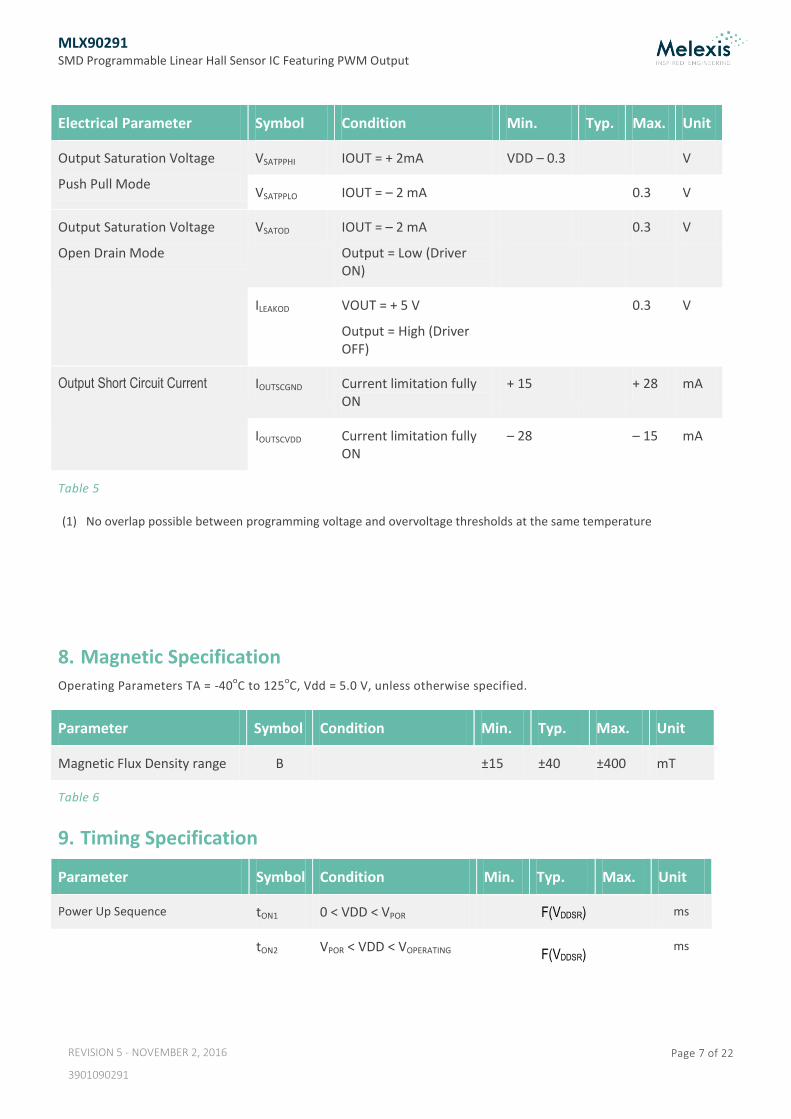
12.2. Output mode configuration (OUTMODE)
OUTMODE configures the output driver.
MLX90291 SMD Programmable Linear Hall Sensor IC Featuring PWM Output
Page 12 of 22
REVISION 5 - NOVEMBER 2, 2016
3901090291
OUTMODE Output Driver
0 PWM Open-drain
1 PWM Push-pull
Table 11 Output configuration
12.3. Sensitivity programming (ROUGHGAIN, FINEGAIN)
ROUGHGAIN[2:0]
This 3-bit register controls the gain of the pre-amplifier.
• The Most Significant Bits enables the PREAMP block, which gives an gain of 4.3 . Enabling this PREAMP uses 2mA extra supply current on top of the specified IDD.
• The 2 LSB control the gain of the MAINAMP
Value Typical Gain
0 15.0
1 21.6
2 31.1
3 44.8
4 64.5
5 92.9
6 133.7
7 192.6
Table 12 ROUGHGAIN versus amplifier gain
FINEGAIN[12:0]
Value defines the digital gain adjustment
• The code 1024 corresponds to a gain of 1
• The MSB is the sign bit which acts as a polarity bit
• FINEGAIN gain range is from -3.9999 to +3.99999

MLX90291 SMD Programmable Linear Hall Sensor IC Featuring PWM Output
Page 13 of 22
REVISION 5 - NOVEMBER 2, 2016
3901090291
12.4. Offset / output quiescent voltage programming (XA, YA)
XA[13:0]
PWM mode: Offset trimming before FINEGAIN block
Switch mode: Threshold for the output to switch
YA[14:0]
PWM mode: Offset trimming after FINEGAIN block
Switch mode: Hysteresis for the output to switch
Both parameters together define the zero Gauss point in PWM mode
In switch mode, XA is used to set the threshold and YA to set the hysteresis
Case YA > 0 Case YA < 0 Output State
ADC < 4.XA – 16.YA ADC < 4.XA Set to Zero
ADC > 4.XA ADC > 4.XA - 16.YA Set to One
Otherwise Otherwise Unchanged
Table 13 Output state as function of XA and YA in switch mode
12.5. Clamping level programming (CLAMP)
CLAMP[2:0] defines the clamping level of the PWM output
CLAMP Minimal output [%DC] Maximal output [%DC]
0 1 99
1 4 96
2 5 95
3 6 94
4 7 93
5 8 92
6 9 91
7 10 90
Table 14 CLAMP parameter versus output.

MLX90291 SMD Programmable Linear Hall Sensor IC Featuring PWM Output
Page 14 of 22
REVISION 5 - NOVEMBER 2, 2016
3901090291
12.6. Bandwidth and filter programming (FILTCODE)
FILTCODE[3:0] allows adjusting the internal bandwidth of the sensor in order to optimize for speed or resolution.
FILTCODE Cutt off frequency [Hz] Attenuation [dB] Tau [ms]
2 557 -8.0 0.29
3 279 -11.2 0.57
4 139 -14.4 1.14
5 70 -18.1 2.29
6 35 -22.4 4.57
7 17 -27.1 9.14
8 9 -32.3 18.29
9 4 -38.1 36.57
Table 15: FILTCODE settings PWM mode
12.7. Current limitation (OUTSLOPE)
2 Bit register to set the current limitation for slew rate control
OUTSLOPE Current limitation [mA]
0 4
1 6
2 11
3 20
Table 16 Current limitation
12.8. PWM Mode duty cycle definition (DCDEF)
The PWM duty cycle definition is as follows.

MLX90291 SMD Programmable Linear Hall Sensor IC Featuring PWM Output
Page 15 of 22
REVISION 5 - NOVEMBER 2, 2016
3901090291
DCDEF PWM duty cycle definition
0 tLow / (tLow + tHigh)
1 tHigh / (tLow + tHigh)
Table 17 PWM duty cycle definition
Period 1 Period 2
OUT
DCDEF=1
tON
tOFF
OUT
Time
Period 1 Period 2
OUT
DCDEF=0
tON
tOFF
OUT
Time
Figure 1: Two different PWM modes
VDD
OUT
POWER UP INIT NORMAL OPERATION
OUT
DCDEF=0
DCDEF=1
0V
5V
VOPERATING
Rising output voltage due to
external pull-up resistor
Figure 2: Power-on behavior of the two different modes
12.9. Sensitivity and temperature drift programming (TC1ST, TC2ND)
TC1ST[6:0]
Programming first order sensitivity temperature drift

MLX90291 SMD Programmable Linear Hall Sensor IC Featuring PWM Output
Page 16 of 22
REVISION 5 - NOVEMBER 2, 2016
3901090291
Value Typical 1st order TC
0 +2740ppm/°C
63 or 64 0ppm/°C
127 -2950ppm/°C
Table 18 : TC1ST parameter
TC2ND[5:0]
Programming second order sensitivity temperature drift
Value Typical 2nd order TC
0 or 32 0 ppm/°C²
31 +6.8 ppm/°C²
63 -6.1 ppm/°C²
Table 19 : TC2ND parameter
12.10. Offset temperature drift programming (OFFDRIFT)
OFFDRIFT[5:0] parameter defines the offset behaviour over temperature (1st order)
Value Offset drift correction
0 or 32 0 mV/°C
31 +0.9 mV/°C
63 -0.9 mV/°C
Table 20 : OFFDRIFT parameter versus correction

MLX90291 SMD Programmable Linear Hall Sensor IC Featuring PWM Output
Page 17 of 22
REVISION 5 - NOVEMBER 2, 2016
3901090291
12.11. Functional Mode (SWITCH)
Value Mode
0 PWM output mode
1 Switch output mode
Table 21 : SWITCH parameter
12.12. Polarity (PLATEPOL)
PLATEPOL parameter changes the sign of the measured sensitivity Default value = 0
12.13. Attenuator (ATTN2P5)
Switch to control the attenuation block in the signal path. Enabling this block reduces the signal by a factor of 4.5. Enabling this attenuator together with the PREAMP block gives the lowest noise at a cost of 2mA with the full signal amplification to be the same.
Value ATTN2P5
0 Attenuation factor = 1
1 Attenuation factor = 4.5
Table 22 : Attenuation settings
12.14. Customer ID (CSTID)
16-bit customer programmable ID
13. Recommended Application Diagrams
13.1. Resistor and Capacitor Values
CLAMP[2:0] defines the clamping level of the PWM output
Part Description Value Unit
C1 Decoupling, EMI, ESD 10 nF

MLX90291 SMD Programmable Linear Hall Sensor IC Featuring PWM Output
Page 18 of 22
REVISION 5 - NOVEMBER 2, 2016
3901090291
C2 Supply capacitor, EMI, ESD
100 nF
R1 Pull up or pull down resistor
4.7 kΩ
Table 23 : Resistive and capacitive values for the recommended application diagrams.
13.2. Pull down resistor for diagnostic low
5
VDD
VSS
TEST4
OUT TEST5
TEST1
TEST2
TEST3 6
7
8
4
3
2
1
MLX90291
+5V
PWM Output
GND
R1
C2
C1
Figure 3: Diagnostic low
13.3. Pull up resistor for diagnostic high
5
VDD
VSS
TEST4
OUT TEST5
TEST1
TEST2
TEST3 6
7
8
4
3
2
1
MLX90291
+5V
PWM Output
GND
R1
C2
C1
Figure 4: Diagnostic high
14. Package Information

MLX90291 SMD Programmable Linear Hall Sensor IC Featuring PWM Output
Page 19 of 22
REVISION 5 - NOVEMBER 2, 2016
3901090291
14.1. SOIC8 Package Dimensions
0.19
0.25
NOTES:
All dimensions are in millimeters (angles in degrees).
* Dimension does not include mold flash, protrusions or
gate burrs (shall not exceed 0.15 per side).
** Dimension does not include interleads flash or protrusion
(shall not exceed 0.25 per side).
*** Dimension does not include dambar protrusion.
Allowable dambar protrusion shall be 0.08 mm total in
excess of the dimension at maximum material condition.
Dambar cannot be located on the lower radius of the foot.
5.84
6.20**
1.27 TYP
4.80
4.98*
1.55
1.73
0.127
0.250
1.40
1.55
0.35
0.49***
3.81
3.99**
0°
8°
0.41
0.89
Figure 5: Package dimensions
14.2. SOIC8 Pin Out and Marking
Marking :
Part Number MLX90291 (3 digits)
291
Die Version (2 digits)
123456 Lot number (6 digits)
Week Date code (2 digits)
Year Date code (2 digits)
YY WW
BC
VD
D
OU
T
TE
ST
1
1
VS
S
TE
ST
4
8
4
5
291BC
123456
YYWW
TE
ST
3
TE
ST
5
TE
ST
2
Figure 6: Pin out and marking

MLX90291 SMD Programmable Linear Hall Sensor IC Featuring PWM Output
Page 20 of 22
REVISION 5 - NOVEMBER 2, 2016
3901090291
14.3. SOIC8 Hall plate positioning
VD
D
OU
T
TE
ST
1
1V
SS
TE
ST
4
8
4
5
TE
ST
3
TE
ST
5
TE
ST
2
Package centerHall sensor position
0.6mm
Figure 7: Hall Plate positioning

MLX90291 SMD Programmable Linear Hall Sensor IC Featuring PWM Output
Page 21 of 22
REVISION 5 - NOVEMBER 2, 2016
3901090291
15. Standard Information
Our products are classified and qualified regarding soldering technology, solderability and moisture sensitivit y level according to standards in place in Semiconductor industry.
For further details about test method references and for compliance verification of selected soldering method for product integration, Melexis recommends reviewing on our web site the General Guidelines soldering recommendation. For all soldering technologies deviating from the one mentioned in above document (regarding peak temperature, temperature gradient, temperature profile etc), additional classification and qualification tests have to be agreed upon with Melexis.
For package technology embedding trim and form post-delivery capability, Melexis recommends to consult the dedicated trim&form recommendation application note: lead trimming and forming recommendations
Melexis is contributing to global environmental conservation by promoting lead free solutions. For more information on qualifications of RoHS compliant products (RoHS = European directive on the Restriction Of the use of certain Hazardous Substances) please visit the quality page on our website: http://www.melexis.com/en/quality-environment
16. ESD Precautions Electronic semiconductor products are sensitive to Electro Static Discharge (ESD). Always observe Electro Static Discharge control procedures whenever handling semiconductor products.
17. Revision History Table
06/10/2016 New template
Table 24
18. Contact
For the latest version of this document, go to our website at www.melexis.com. For additional information, please contact our Direct Sales team and get help for your specific needs:
Europe, Africa Telephone: +32 13 67 04 95
Email : [email protected]
Americas Telephone: +1 603 223 2362
Email : [email protected]
Asia Email : [email protected]

MLX90291 SMD Programmable Linear Hall Sensor IC Featuring PWM Output
Page 22 of 22
REVISION 5 - NOVEMBER 2, 2016
3901090291
19. Disclaimer The information furnished by Melexis herein (“Information”) is believed to be correct and accurate. Melexis disclaims (i) any and all liability in connection with or arising out of the furnishing, performance or use of the technical data or use of the product(s) as described herein (“Product”) (ii) any and all liability, including without limitation, special, consequential or incidental damages, and (iii) any and all warranties, express, statutory, implied, or by description, includ ing warranties of fitness for particular purpose, non-infringement and merchantability. No obligation or liability shall arise or flow out of Melexis’ rendering of technical or other services. The Information is provided "as is” and Melexis reserves the right to change the Information at any time and without notice. Therefore, before placing orders and/or prior to designing the Product into a system, users or any third party should obtain the latest version of the relevant information to verify that the information being relied upon is current. Users or any third party must further determine the suitability of the Product for its application, including the level of reliability required and determine whether it is fit for a particular purpose. The Information is proprietary and/or confidential information of Melexis and the use thereof or anything described by the Information does not grant, explicitly or implicitly, to any party any patent rights, licenses, or any other intellectual property rights. This document as well as the Product(s) may be subject to export control regulations. Please be aware that export might require a prior authorization from competent authorities. The Product(s) are intended for use in normal commercial applications. Unless otherwise agreed upon in writing, the Product(s ) are not designed, authorized or warranted to be suitable in applications requiring extended temperature range and/or unusual environmental requirements. High reliability applications, such as medical life-support or life-sustaining equipment are specifically not recommended by Melexis. The Product(s) may not be used for the following applications subject to export control regulations: the development, product ion, processing, operation, maintenance, storage, recognition or proliferation of 1) chemical, biological or nuclear weapons, or for the development, production, maintenance or storage of missiles for such weapons: 2) civil firearms, including spare parts or ammunition for such arms; 3) defense related products, or other material for military use or for law enforcement; 4) any applications that, alone or in combination with other goods, substances or organisms could cause serious harm to persons or goods and that can be used as a means of violence in an armed conflict or any similar violent situation. The Products sold by Melexis are subject to the terms and conditions as specified in the Terms of Sale, which can be found at https://www.melexis.com/en/legal/terms-and-conditions. This document supersedes and replaces all prior information regarding the Product(s) and/or previous versions of this document. Melexis NV © - No part of this document may be reproduced without the prior written consent of Melexis. (2016) ISO/TS 16949 and ISO14001 Certified