Embed Size (px)
Citation preview
�
�
Jakob Reichel and Vladan Vuletic: Atom Chips — Chap. reichel7552c01 — 2010/12/2 — page 3 — le-tex
�
�
�
�
�
�
3
1From Magnetic Mirrors to Atom Chips1)
Andrei Sidorov and Peter Hannaford
1.1Introduction
Following the advent of laser cooling and trapping techniques in the 1980s, a newexciting area of research, ‘atom chips’, has emerged in which sophisticated micron-scale structures on planar substrates are produced utilizing the latest technologicaldevelopments in lithography and nanofabrication. These complex microstructuresproduce tiny magnetic field configurations which can trap, cool, and manipulateensembles of ultra-cold atoms in the vicinity of a surface. Scaling down the di-mensions of atom trapping geometry offers extended possibilities for the produc-tion and control of Bose–Einstein condensates (BECs). Enormous progress on thegeneration of BECs and quantum degenerate Fermi gases, on-chip matter–waveinterferometers, and integrated detectors has been made in the last few years.
In the second section of this article we trace the historical evolution of this newfield, from the first surface-based atom optical elements – magnetic mirrors – to thepresent-day micro-fabricated structures on a substrate – atom chips. In Section 1.3we present the basic principles of magnetic mirrors for cold atoms and describe dif-ferent types of magnetic mirror. Section 1.4 describes the production of a BEC ona permanent magnetic film atom chip; the application of this atom chip to probethe topology of magnetic fields using RF spectroscopy and to study the adiabaticsplitting of a BEC in a double well for sensing asymmetric potentials; and inves-tigations of the spatially dependent relative phase evolution of a two-componentBEC. Finally, in Section 1.5 we describe a permanent magnetic lattice on an atomchip for trapping and manipulating multiple arrays of ultra-cold atoms and quan-tum degenerate gases.
1) We dedicate this article to the memory of our friend and colleague Geoffrey I. Opat.
Atom Chips. Edited by Jakob Reichel and Vladan VuleticCopyright © 2011 WILEY-VCH Verlag GmbH & Co. KGaA, WeinheimISBN: 978-3-527-40755-2
�
�
Jakob Reichel and Vladan Vuletic: Atom Chips — Chap. reichel7552c01 — 2010/12/2 — page 4 — le-tex
�
�
�
�
�
�
4 1 From Magnetic Mirrors to Atom Chips
1.2Historical Background
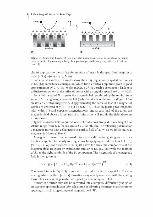
In 1983 Opat [1] proposed the idea of using periodic arrays of electric fields on aplanar substrate to reflect beams of polar molecules in a matter–wave interferom-eter. Almost a decade later the Melbourne group [2] reported the reflection of abeam of chloromethane (CH3Cl) molecules from the exponentially decaying elec-tric field above a periodic array of electrodes of alternating polarity.2) Opat and co-workers [3] then extended these ideas to periodic arrays of magnetic fields to createa surface-based mirror for reflecting beams of laser-cooled atoms (Figure 1.1a). Asslowly moving atoms in positive (or ‘low-field seeking’) magnetic states approachthe periodic magnetic structure they experience an exponentially increasing mag-netic field, with decay length a/2π (where a is the period), and for sufficiently largemagnetic fields the atoms are repelled by the structure. A number of schemes [3]were proposed for producing the periodic magnetic structures, including the useof arrays of magnets of alternating polarity, periodic magnetic fields ‘recorded’ onferromagnetic substrates as in sound recording, and planar arrays of parallel wiresalternately carrying electric current in opposite directions. Methods for fabricatingthe surface-based microstructures were suggested including lithographical tech-niques used in the electronics industry.
The first magnetic mirror for cold atoms was realized in 1995 by Roach et al. [4]by recording sinusoidal signals onto a magnetic audio-tape and observing theretroflection of laser-cooled rubidium atoms from the recorded structure. Soonafter, Sidorov et al. [5] in Melbourne reported the retroreflection of cold cesiumatoms from a 2-mm-period planar array of Nd-Fe-B magnets of alternating polarity.In 1997 the Sussex group demonstrated the focusing and multiple reflection ofcold atoms bouncing on a curved magnetic mirror made from a concave-shapedfloppy disk or video tape [6, 7].
One of the major challenges was to be able to scale the magnetic structuresdown to micron-scale periods, in order to produce a hard mirror with very shortdecay length and minimal finite-size effects. This problem was basically solvedwhen it was shown [8] that a grooved periodic magnetic structure produces amagnetic field distribution that is essentially the same as that above an array ofmagnets of alternating polarity. The Melbourne group subsequently demonstrat-ed the specular reflection of cold atoms from a 1-μm-period magnetic mirrorconstructed from micro-fabricated grooved structures coated with perpendicular-ly magnetized film [9, 10]. The scaling down of the period to 1 μm representeda significant advance in the miniaturization of surface-based atom optical ele-ments.
In 1999 the Melbourne [11] and Harvard/Orsay/Gaithersburg [12] groups report-ed a magnetic mirror for cold atoms constructed from a planar array of current-carrying conductors lithographically patterned on a silicon wafer or a sapphire sub-
2) The beam of slowly moving polar molecules was produced in a gravity-assisted molecular beamline experiment (GAMBLE).
�
�
Jakob Reichel and Vladan Vuletic: Atom Chips — Chap. reichel7552c01 — 2010/12/2 — page 5 — le-tex
�
�
�
�
�
�
1.2 Historical Background 5
strate. A feature of this type of magnetic mirror is that the magnetic field may bereadily varied, switched or modulated by varying the current in the conductors.Such magnetic mirrors were the first micro-fabricated surface-based optical ele-ments for cold atoms and represented a significant step towards the developmentof more sophisticated atom chips based on micro-fabricated current-carrying con-ductors on a substrate [13–15].
In an earlier paper, Weinstein and Libbrecht [16] at CalTech had proposed variousplanar current-carrying wire geometries for constructing microscopic electromag-netic traps for cold atoms including the use of superconducting wire structures.In 1998 Vuletic et al. [17] and Fortágh et al. [18] in Munich demonstrated 3D mi-crotraps for cold atoms based on a combination of electromagnets and permanentmagnets or current-carrying conductors, and Drndic et al. [19] at Harvard reportedthe fabrication of micro-electromagnetic traps with geometries proposed in [16].In 1999 the Munich group [20] reported the use of surface magnetic microtrapsbased on a ‘U’-shaped wire quadrupole microtrap and a ‘Z’-shaped wire Ioffe–Pritchard (IP) microtrap, with non-zero potential minimum to eliminate spin-fliplosses, for the trapping of cold atoms on a substrate. Soon after, other groups [21–24] demonstrated the guiding of laser-cooled atoms by current-carrying wires, andDavis [25] proposed the use of permanent magnetic structures as miniature wave-guides to transport cold atoms on a substrate. In 2000 the Innsbruck group [26]reported the trapping and guiding of cold atoms using a micro-fabricated circuiton a substrate, which they called an ‘atom chip’. In the following year the Munichgroup [27] demonstrated a magnetic conveyer belt for transporting and mergingcold atoms on an atom chip.
A major breakthrough came at the International Conference on Laser Spec-troscopy in Snowbird in 2001 when Hänsel et al. [28] from Munich and Ott et al. [29]from Tübingen simultaneously announced the realization of a Bose–Einstein con-densate (BEC) of 87Rb atoms in a current-carrying magnetic microtrap on an atomchip. The use of miniature magnetic microtraps allowed the scaling down of theelectric currents required to produce a BEC and the scaling up of the trap con-finement and elastic collision rate, thus greatly simplifying and speeding up theproduction of a BEC. In 2006 Aubin et al. ([30], Chapter 12) in Toronto realized adegenerate Fermi gas of 40K atoms on an atom chip by sympathetic cooling withultra-cold 87Rb atoms.
One of the next big challenges was to see if it was possible to perform coherenceor interference experiments on ultra-cold atoms trapped on an atom chip at dis-tances close to the surface (Chapters 4 and 5). In 2004 Treutlein et al. [31] in Munichreported the coherent manipulation of two hyperfine states of ultra-cold 87Rb atomsin a current-carrying magnetic microtrap, with coherence times exceeding 1 s. Thisopened the way for Ramsey interferometry and miniature atomic clocks on an atomchip ([32], Chapter 8). However, on-chip interferometry by spatially splitting thecondensate proved to be more challenging owing to difficulties of phase preserva-tion and control of the condensate. In 2005 the MIT/Harvard groups [33] dynami-cally split a condensate by deforming a single-well magnetic trap into a double-wellpotential, but non-adiabatic evolution in a quartic potential during the splitting
�
�
Jakob Reichel and Vladan Vuletic: Atom Chips — Chap. reichel7552c01 — 2010/12/2 — page 6 — le-tex
�
�
�
�
�
�
6 1 From Magnetic Mirrors to Atom Chips
process led to an unpredictable relative phase. A major breakthrough came whenthe Heidelberg/Vienna group demonstrated a phase-preserving splitting schemebased on RF-induced adiabatic potentials ([34], Chapter 7), which allowed accu-rate control over the splitting process and the observation of reproducible inter-ference fringes with a deterministic phase. In the same year the Boulder/Harvardgroups [35] achieved splitting, reflection, and recombining of condensate atoms ina Michelson interferometer using a standing-wave light field in a waveguide on achip. In 2007 the MIT/Harvard groups [36] reported the observation of phase co-herence between two separated BECs on an atom chip for times up to about 200 msafter splitting the condensate. In 2009 the Munich group [37] demonstrated the co-herent manipulation of BECs in a state-dependent potential with microwave fieldson an atom chip, allowing the on-chip generation of multi-particle entanglementand quantum-enhanced metrology with spin-squeezed states [38] (Chapter 8).
Very recently, Deutsch et al. [39] in Paris have reported coherence times as longas 58 s in a Ramsey interferometer experiment on 87Rb atoms trapped on an atomchip. The long coherence times are interpreted in terms of a spin self-rephasingmechanism induced by an identical spin rotation effect that occurs during collisonsin the forward direction between two identical particles [40]
In parallel developments Sinclair et al. [41] in London produced a BEC on apermanent-magnet atom chip based on periodically magnetized videotape and Hallet al. [42, 43] in Melbourne produced a BEC in a microtrap on a TbGdFeCo perma-nent magnetic film atom chip. BECs have since been produced in microtraps on aCo-Cr-Pt hard disk [44] and on a Fe-Pt magnetic foil atom chip [45]. In 2007 Whit-lock et al. in Amsterdam [46, 47] constructed a 2D asymmetric magnetic latticewith periods of 22 and 36 μm in orthogonal directions on a Fe-Pt film atom chipand the Melbourne group [48, 49] constructed a 1D 10-μm-period magnetic latticeon a TbGdFeCo film atom chip. Both groups demonstrated the loading of ultra-cold atoms into multiple sites of the permanent magnetic lattice. Magnetic latticescan be readily scaled to have a very large number of lattice sites and could form thebasis of storage registers for quantum information processing.
Superconducting wires offer the prospect of an extremely low noise environmentfor trapped ultra-cold atoms. In 2006 Nirrengarten et al. ([50] and Chapter 10) inParis reported the trapping of ultra-cold atoms on a superconducting atom chip andthe following year Mukai et al. [51] in Tokyo demonstrated the trapping of atoms ona persistent supercurrent atom chip. In 2008 the Paris group [52] realized a BECon a superconducting atom chip and the Tübingen group [53] demonstrated theMeissner effect using ultra-cold atoms trapped by a superconducting wire on anatom chip. The development of superconducting atom chips also opens the way tonew fundamental quantum physics experiments such as the coupling of a BEC tosuperconducting loops [54].
Comprehensive review articles on magnetic mirrors, microtraps and atomchips for ultra-cold atoms and quantum degenerate gases have been publishedby Hinds and Hughes [55], Folman et al. [13], Reichel [14], and Fortágh and Zim-mermann [15].
�
�
Jakob Reichel and Vladan Vuletic: Atom Chips — Chap. reichel7552c01 — 2010/12/2 — page 7 — le-tex
�
�
�
�
�
�
1.3 Magnetic Mirrors for Cold Atoms 7
1.3Magnetic Mirrors for Cold Atoms
1.3.1Basic Principles
We first consider an atom with magnetic dipole moment μ moving in an inhomo-geneous magnetic field B(x , y , z). If the rate of change of the direction of B(x , y , z)as seen by the moving atom is slow compared with the atom’s Larmor frequency,then the orientation of μ can adiabatically follow the direction of the magnetic fieldand the position-dependent interaction potential Uint(x , y , z) D �μ � B(x , y , z)exerts a gradient or Stern–Gerlach force on the atom given by Fgrad D r(μ � B)D �mF gFμBrB(x , y , z), where mF is the magnetic quantum number, gF theLandé factor, and μB the Bohr magneton. Thus, atoms oriented in positive (orlow-field seeking) magnetic states (mFgF > 0) experience a negative force andare repelled by an increasing magnetic field, while atoms in negative (or high-field seeking) magnetic states (mFgF < 0) are attracted by an increasing magneticfield.
We now consider the inhomogeneous magnetic field produced by a periodic ar-ray of magnets having alternating perpendicular magnetization M(y , z) D CMz
and �Mz in the y direction with period a (Figure 1.1a). For an infinite array of long,thick (t � a/2π) magnets of width a/2, the components and the magnitude of themagnetic field above the array are given by [5]
By (y , z) D B0e�k z�
sin k y � 1/3e�2k z sin 3k y C . . .�
,
Bz(y , z) D B0e�k z�
cos k y � 1/3e�2k z cos 3k y C . . .�
,
jB(y , z)j D B0e�k z�
1 � 1/3e�2k z cos 2k y C . . .�
, (1.1)
where k D 2π/a, and B0 D 8Mz (Gaussian units) is a characteristic surface mag-netic field. For distances z � a/4π, Eq. (1.1) reduce to�
By (y , z)I Bz(y , z)� � hB0e�k z sin k y I B0e�k z cos k y
i, jBj � B0e�k z .
(1.2)
Equation (1.2) indicates that for distances z � a/4π the magnitude of the mag-netic field is no longer dependent on y and falls off exponentially with distance z,with decay length k�1 D a/2π, while the direction of the magnetic field for a giv-en distance z rotates in the y z-plane with period a as y varies (Figure 1.1a). Thus,an atom in a weak-field seeking magnetic state moving adiabatically towards thesurface will be repelled by the exponentially increasing magnetic field, and if itsmagnetic potential energy exceeds the kinetic energy with which it approaches thesurface the atom will be reflected. For a pure single-harmonic potential, Eq. (1.2)holds for all distances z above the array. For an array of magnets of finite thick-ness t, B0 in Eq. (1.2) is replaced by Bs D (1 � e�k t)B0 [10, 56]. The distance of
�
�
Jakob Reichel and Vladan Vuletic: Atom Chips — Chap. reichel7552c01 — 2010/12/2 — page 8 — le-tex
�
�
�
�
�
�
8 1 From Magnetic Mirrors to Atom Chips
N
S
N
S
N
S
N
S
S
N
S
N
S
N
S
N
N N N N N
S S S S S
atom atom
(a) (b)a a
z
yB B
Figure 1.1 Schematic diagram of (a) a magnetic mirror consisting of perpendicularly magne-tized elements of alternating polarity, (b) a grooved perpendicularly magnetized microstruc-ture [10].
closest approach to the surface for an atom of mass M dropped from height h isz0 � (a/2π) ln(mFgF μBBs/M gh).
For small distances (z < a/4π) above the array, higher-order spatial harmonicsin Eq. (1.1) contribute a corrugation, which have a relative amplitude given to goodapproximation by C � 1/3(M gh/mF gF μBB0)2 [56]. Such a corrugation leads to adiffusive component in the reflected atoms with an angular spread Δθrms �
p2C .
For a finite array of N magnets the magnetic field produced by the semi-infinitearray of ‘missing’ magnets on the left (right) hand side of the mirror (Figure 1.1a)creates an effective magnetic field approximately the same as that of a magnet ofwidth a/4 centered at y D �N a/4 (CN a/4) [5]. Thus, by placing two magnets,with width a/4 and opposite magnetizations, one at each end of the array, themagnetic field above a large area of a finite array will mimic the field above aninfinite array.
Typical magnetic fields required to reflect cold atoms dropped from a height h D20 mm range from 47 G for cesium to 2.5 G for lithium. The reflecting potential fora magnetic mirror with a characteristic surface field of B0 D 4.2 kG (thick Nd-Fe-Bmagnets) is 24 μeV (280 mK).
A magnetic mirror may be turned into a spatial diffraction grating, or a diffrac-tive beam splitter, for slowly moving atoms by applying a uniform bias field B1z
(or B1y ) [3, 57]. For distances z � a/4π above the array, the components of themagnetic field are given by expressions similar to Eq. (1.2) but with the additionof B1z to the right-hand side of the Bz component. The magnitude of the magneticfield is then given by
jB(y , z)j ��
B21z C 2B1z B0e�k z cos k y C B2
0e�2k z�1/2
. (1.3)
The second term in Eq. (1.3) is periodic in y, and may act as a spatial diffractiongrating, while the third (mirror) term dies away rapidly compared with the gratingterm. This leads to the periodic corrugated pattern in Figure 1.11d.
A magnetic mirror may also be converted into a temporal diffraction grating, oran ‘acousto-optic modulator’, for cold atoms by vibrating the magnetic structure orapplying an oscillating orthogonal magnetic field [58].
�
�
Jakob Reichel and Vladan Vuletic: Atom Chips — Chap. reichel7552c01 — 2010/12/2 — page 9 — le-tex
�
�
�
�
�
�
1.3 Magnetic Mirrors for Cold Atoms 9
1.3.2Experimental Realization of Magnetic Mirrors
1.3.2.1 Macroscopic Array of Rare-Earth Magnets of Alternating PolarityTo test the basic principles of the magnetic mirror, we first constructed a planarperiodic array of 18 1-mm-wide Nd-Fe-B magnets of alternating polarity, with a0.5-mm-wide magnet at each end to compensate for end-effects [5]. Hall probemeasurements indicate that the By and Bz components above the array exhibita sine and cosine dependence on y, while the magnitude of the magnetic fieldshows an exponential dependence on z, given by Eq. (1.2), with a D 2.06 mm andB0 D 4.2 kG.
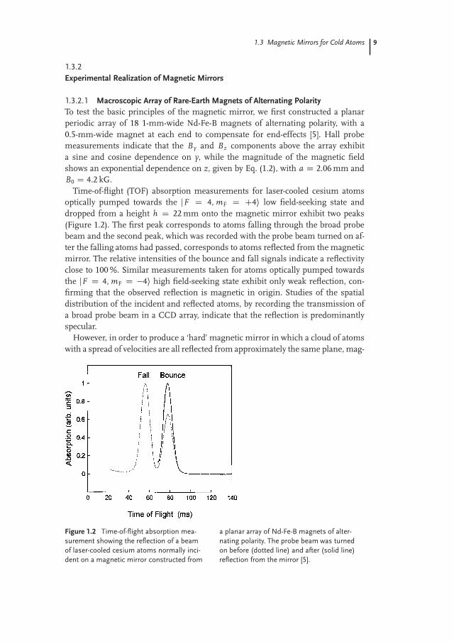
Time-of-flight (TOF) absorption measurements for laser-cooled cesium atomsoptically pumped towards the jF D 4, mF D C4i low field-seeking state anddropped from a height h D 22 mm onto the magnetic mirror exhibit two peaks(Figure 1.2). The first peak corresponds to atoms falling through the broad probebeam and the second peak, which was recorded with the probe beam turned on af-ter the falling atoms had passed, corresponds to atoms reflected from the magneticmirror. The relative intensities of the bounce and fall signals indicate a reflectivityclose to 100 %. Similar measurements taken for atoms optically pumped towardsthe jF D 4, mF D �4i high field-seeking state exhibit only weak reflection, con-firming that the observed reflection is magnetic in origin. Studies of the spatialdistribution of the incident and reflected atoms, by recording the transmission ofa broad probe beam in a CCD array, indicate that the reflection is predominantlyspecular.
However, in order to produce a ‘hard’ magnetic mirror in which a cloud of atomswith a spread of velocities are all reflected from approximately the same plane, mag-
Figure 1.2 Time-of-flight absorption mea-surement showing the reflection of a beamof laser-cooled cesium atoms normally inci-dent on a magnetic mirror constructed from
a planar array of Nd-Fe-B magnets of alter-nating polarity. The probe beam was turnedon before (dotted line) and after (solid line)reflection from the mirror [5].
�
�
Jakob Reichel and Vladan Vuletic: Atom Chips — Chap. reichel7552c01 — 2010/12/2 — page 10 — le-tex
�
�
�
�
�
�
10 1 From Magnetic Mirrors to Atom Chips
netic structures with much smaller periods, preferably on the scale of a micron, arerequired.
1.3.2.2 Micro-Fabricated Grooved Magnetic MirrorsThe fabrication of an array of magnets of alternating polarity with periods downto 1 μm presents a considerable technical challenge. Model calculations (e.g., Fig-ure 1.10c) show that a grooved perpendicularly magnetized structure (Figure 1.1b)produces a magnetic field distribution the same as that above an array of mag-nets of alternating polarity (Figure 1.1a), but with the characteristic surface field B0
reduced by a factor of two [10]. Thus, the grooves behave as missing magnets ofopposite polarity to that of the tiny magnets in the protrusions. Grooved magneticstructures may be readily fabricated with micron-scale periods and with excellentsurface topology using micro-fabrication techniques such as electron-beam litho-graphy, photolithography, or reactive ion etching.
We have found that by using perpendicularly magnetized films, such as Co80Cr20
or Tb6Gd10Fe80Co4, deposited on a grooved non-magnetic substrate, it is possibleto fabricate high-quality magnetic structures with periods down to 1 μm [9, 10, 59].Magnetic force microscopy (MFM) scans of the magnetic microstructures showthat the variation of Bz with y is approximately sinusoidal, even at distances veryclose (z � 0.05 μm) to the surface. The sinusoidal shape at small distances isattributed to rounding of the top edges of the groove walls, which reduces the con-tribution of higher order spatial harmonics (Eq. (1.1)). The magnitude of the Bz
component is found to decrease exponentially with distance z, with decay lengtha/2π. For grooved microstructures coated with ferromagnetic Co80Cr20 film [9, 10],the MFM scans show evidence of domain structure in the regions above the pro-trusions, with a size � 0.5 μm, while at distances greater than 0.5 μm the mag-netic inhomogeneities have decayed away, consistent with a domain size of about0.5 μm. Hysteresis loop measurements for the Co80Cr20 films exhibit a rhombo-hedral shape with a coercivity of about 1 kOe and a remanent magnetization of�25 % of the saturation magnetization (typical of Co80Cr20), indicating that notall the domains remain oriented after the magnetizing process. The saturationmagnetization for Co80Cr20 is � 5 kG; so for grooved microstructures with a D1 μm and t D 0.2 μm the characteristic surface field is estimated to be Bs �280 G.
TOF absorption measurements for laser-cooled atoms dropped from a heighth D 18 mm onto 15� 15 mm2 Co80Cr20 magnetic microstructures show strong re-flection signals similar to Figure 1.2. For Cs jF D 4, mF D C4i atoms incident onan a D 1 μm microstructure the distance of closest approach is z0 � 0.3 μm. Mea-surements of the spatial distribution of the atom cloud at different times beforeand after reflection yield a value for the angular spread introduced by the reflectionfrom the grooved mirror of Δθrms D (16 ˙ 20) mrad. To reduce the uncertaintiesfurther would require reducing the initial transverse velocity of the atoms, for ex-ample, by collimating the atom cloud or by reducing the temperature in the x yplane, or by extending the spatial distribution measurements out to much longertimes after the first reflection.
�
�
Jakob Reichel and Vladan Vuletic: Atom Chips — Chap. reichel7552c01 — 2010/12/2 — page 11 — le-tex
�
�
�
�
�
�
1.3 Magnetic Mirrors for Cold Atoms 11
The quality of the grooved magnetic microstructures could be improved, for ex-ample, by using ferrimagnetic Tb6Gd10Fe80Co4 films [59] instead of the Co80Cr20
film. MFM images taken for Tb6Gd10Fe80Co4 films show excellent magnetic ho-mogeneity, with no evidence of domain structure. Such films have a magnetization4πMr � 2.8 kG, which for an a D 1 μm, t D 0.2 μm magnetic microstructuregives a characteristic surface field Bs � 640 G. Our calculations indicate that forthe above parameters and using a small bias field to compensate end-effects andstray magnetic fields it should be possible to reduce corrugations so that the angu-lar spread Δθrms < 1 mrad. This type of grooved magnetic microstructure appearsto be the most promising approach to date for producing high-quality magneticmirrors with micron-scale periods.
Although it is possible to fabricate grooved magnetic mirrors with periods small-er than 1 μm the incident atoms will then start to approach so close to the surfacethat van der Waals forces and the Casimir–Polder force become significant [13],(Chapters 4 and 5).
1.3.2.3 Micro-Fabricated Array of Current-Carrying ConductorsMagnetic mirrors based on periodic arrays of current-carrying conductors have anumber of features. Each element in the series array carries the same current andhence produces the same magnetic flux, allowing the production of very flat mir-rors, and the ability to control the current allows the magnetic field to be varied,switched, or modulated.
For an infinite array of narrow wire conductors alternately carrying equal cur-rents I in opposite directions, the components and the magnitude of the magneticfield above the array are given by expressions similar to Eq. (1.1), but with a char-acteristic surface field B 0
0 D 8πI/a and a geometrical coefficient of unity insteadof ‘1/3’ in the second-order term [11]. For a finite array of wires, the magnetic fielddistribution above the array may approximate the infinite case by adding two com-pensating wires each carrying half the normal current to the ends of the array athalf the normal spacing [11].
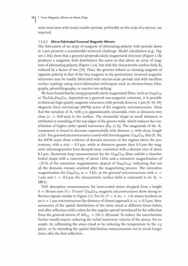
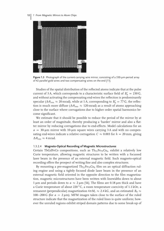
To demonstrate the principle of such a mirror we constructed an a D 330 μmplanar array of 42 parallel gold conductors with two compensating wires on theends (Figure 1.3) prepared on a silicon wafer by UV photolithography and electro-plating techniques [11]. The gold conductors were 60 μm wide, 10 μm thick, and8 mm long.
TOF absorption signals recorded for jF D 4, mF D C4i cesium atoms droppedfrom a height h D 20 mm onto the current-carrying wire mirror when activatedwith 3 A, 12-ms current pulses to coincide with the arrival of the falling atomsindicate a reflectivity close to 100 %. When the duration of the current pulse isreduced to much less than the spread of arrival times of the atoms, the TOF signalsharpens significantly due to ‘velocity filtering’ in the vertical direction. Studiesof the dependence of the reflection signal on current through the wires show areflection threshold at 0.45 A, followed by three steeply rising regions which areidentified as representing the sequential reflection of atoms in the mF D C4 (andC3), C2 andC1 magnetic states.
�
�
Jakob Reichel and Vladan Vuletic: Atom Chips — Chap. reichel7552c01 — 2010/12/2 — page 12 — le-tex
�
�
�
�
�
�
12 1 From Magnetic Mirrors to Atom Chips
Figure 1.3 Photograph of the current-carrying wire mirror, consisting of a 330-μm-period arrayof 42 parallel gold wires and two compensating wires on the end [11].
Studies of the spatial distribution of the reflected atoms indicate that at the pulsecurrent of 3 A, which corresponds to a characteristic surface field of B 0
0 D 230 G,and without activating the compensating end-wires the reflection is predominantlyspecular (Δθrms � 20 mrad), while at 1 A, corresponding to B 0
0 D 77 G, the reflec-tion is much more diffuse (Δθrms � 120 mrad) as a result of atoms approachingclose to the surface where corrugations due to higher order spatial harmonics be-come significant.
We estimate that it should be possible to reduce the period of the mirror by atleast an order of magnitude, thereby producing a ‘harder’ mirror and also a flat-ter mirror by reducing corrugations due to end-effects. Model calculations for ana D 30-μm mirror with 10-μm square wires carrying 3 A and with no compen-sating end-wires indicate a relative corrugation C � 0.003 for h D 20 mm, givingΔθrms � 4 mrad.
1.3.2.4 Magneto-Optical Recording of Magnetic MicrostructuresCertain TbGdFeCo compositions, such as Tb15Fe79Co6, exhibit a relatively lowCurie temperature, allowing magnetic structures to be written with a focussedlaser beam in the presence of an external magnetic field. Such magneto-opticalrecording offers the prospect of writing fine and also complex structures.
By mounting a pre-magnetized Tb15Fe79Co6 film on an optical diffraction rul-ing engine and using a tightly focused diode laser beam in the presence of anexternal magnetic field oriented in the opposite direction to the film magnetiza-tion, magnetic microstructures have been written with linewidths down to about1 μm and periods down to a � 2 μm [56]. The films are 0.18 μm thick and havea Curie temperature of about 220 ıC, a room temperature coercivity of 1.1 kOe, aremanent (perpendicular) magnetization 4πMr � 2.4 kG, and an estimated B0 �100�200 G (for a D 2 μm). MFM images taken close to the surface of the ruledstructure indicate that the magnetization of the ruled lines is quite uniform; how-ever the unruled regions exhibit striped domain patterns due to some break-up of
�
�
Jakob Reichel and Vladan Vuletic: Atom Chips — Chap. reichel7552c01 — 2010/12/2 — page 13 — le-tex
�
�
�
�
�
�
1.4 The Magnetic Film Atom Chip 13
the pre-magnetized regions during the recording process [56]. At larger distances(� 0.5 μm) from the surface the magnetic field gradient due to the striped domainpatterns is found to have decayed away and the MFM scans become approximatelysinusoidal in the y direction, with an exponential fall off with distance z, with decaylength a/2π.
TOF absorption measurements of laser-cooled cesium atoms dropped from aheight h D 25 mm onto recorded magnetic structures exhibit strong reflection sig-nals, and spatial distribution measurements of the reflected atoms indicate that thereflection is predominantly specular. It should be possible to improve the specular-ity by further optimization of the magneto-optical recording process and composi-tion of the alloy.
1.4The Magnetic Film Atom Chip
1.4.1Background
Advances in photolithography and micro-fabrication techniques have led to thedevelopment of miniature surface-based current-carrying elements for the pro-duction of BECs and the precise manipulation of ultra-cold atoms, allowing theconstruction and integration of networks of microtraps, waveguides, and inter-ferometers on the surface of a substrate [13–15, 55]. Miniaturization and scalingdown the dimensions of atom traps allow the use of moderate electric currentsin order to produce large magnetic field gradients and curvatures and hence avery tight confinement of atomic waves. These microstructures greatly increaseelastic collision rates and allow condensates to be produced in just a few secondsof evaporative cooling.
Permanent magnetic materials may also be used to produce magnetic field con-figurations that can trap, guide, and precisely manipulate neutral atoms [10, 25, 60].In a ferromagnetic material the magnetic domains generate magnetic fields whichare equivalent to the fields produced by effective surface current loops flowing per-pendicular to the magnetization vector around the domain edges. In a uniformlymagnetized film with perpendicular anisotropy all the domains are aligned in thesame direction and within the bulk the currents of neighboring domains cancel.At the same time a net effective current flows around the perimeter of the filmwith a magnitude given by the product of the magnetization and the film thickness(Ieff D Mr� t). Using established micro-fabrication techniques such as photolitho-graphy, vapor deposition, or laser ablation, arbitrary shapes of magnetic film canbe fabricated. As examples, a straight edge of a magnet in combination with auniform external magnetic field will generate a 2D quadrupole potential [10] and aZ-shaped edge of a perpendicularly magnetized film will produce an IP magnetictrap [61]. The use of integrated materials (magnetic films, microwires, and electric
�
�
Jakob Reichel and Vladan Vuletic: Atom Chips — Chap. reichel7552c01 — 2010/12/2 — page 14 — le-tex
�
�
�
�
�
�
14 1 From Magnetic Mirrors to Atom Chips
field elements [62]) provides flexibility and extends the capability of integratedatom optics devices.
Various technical limitations can affect applications of current microcircuits onatom chips [13–15]. Large current densities are required to produce large magneticfield gradients and this can lead to excessive heat generation, microwires pealingoff, and broken circuits. Current noise from power supplies increases heating ratesand limits the condensate lifetime. Johnson thermal noise radiated by a micro-wireconductor leads to spin-flips which affect the BEC lifetime [63]. Permanent magnet-ic microstructures can replace current microcircuits on atom chips and overcomemany of these problems.
Typical permanent magnetic films have a relatively large resistance and a thick-ness less than 1 μm which suppress radiated thermal magnetic noise. It is expectedthat permanent magnetic films will produce ultra-stable magnetic potentials andlow heating rates. Magnetic films with perpendicular anisotropy, which are used innew-generation hard disk media, provide additional stability of the magnetic fieldand allow finer magnetic microstructures.
1.4.2BEC on a Magnetic Film Atom Chip
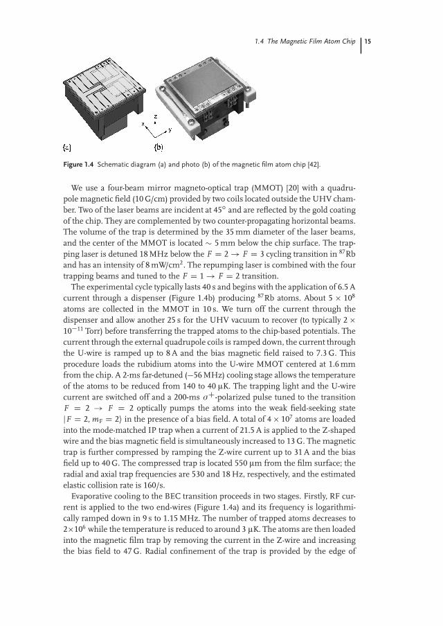
Permanent magnetic microstructures can produce quadrupole magnetic potentialsand with the use of external bias fields can allow adjustment of the position andtightness of the trap. However, the capture volume of the traps is small and thenumber of cold atoms trapped is not sufficient for efficient evaporative cooling. Inorder to improve the efficiency of atom capture we combine the permanent mag-netic film with current-carrying wires using a two-layer structure (Figure 1.4) [43].
An H-shape plus two end-wire structure was machined in a 0.5-mm-thick silverplate and glued to a ceramic plate to form the bottom layer. The wires have a widthof 1 mm and can carry a continuous current of 30 A with an associated temperaturerise of no more than 40 ıC. The H-shape structure can be arranged for both U andZ-shape currents for quadrupole and IP potentials, respectively.
The top layer of the chip is formed by two 300-μm-thick glass slides (40�23 mm2)glued to the silver structure. High magnetic field gradients require a large effec-tive surface current of the magnetic film and hence large values of the magnetiza-tion Mr and/or thickness t. We choose to use ferrimagnetic Tb6Gd10Fe80Co4 filmswhich exhibit strong perpendicular magnetic anisotropy, an almost square hystere-sis loop with a remanent magnetization 4πMr D 2.8 kG, a coercivity 4πHc D4 kOe, and a Curie temperature TC � 300 ıC. The composition of the alloy is cho-sen to be a compromise between the desire to have large magnetization, high coer-civity, and high Curie temperature. One of the slides is coated with a 0.9-μm-thickTb6Gd10Fe80Co4 film (effective current 0.2 A). A long polished edge (Figure 1.4a)together with a bias field generates a quadrupole radial potential. Parallel currentsin the two end-wires (separation 9 mm) provide axial confinement and conversionto a 3D IP trap. Both slides are finally coated with a 100-nm-thick gold film.
�
�
Jakob Reichel and Vladan Vuletic: Atom Chips — Chap. reichel7552c01 — 2010/12/2 — page 15 — le-tex
�
�
�
�
�
�
1.4 The Magnetic Film Atom Chip 15
Figure 1.4 Schematic diagram (a) and photo (b) of the magnetic film atom chip [42].
We use a four-beam mirror magneto-optical trap (MMOT) [20] with a quadru-pole magnetic field (10 G/cm) provided by two coils located outside the UHV cham-ber. Two of the laser beams are incident at 45ı and are reflected by the gold coatingof the chip. They are complemented by two counter-propagating horizontal beams.The volume of the trap is determined by the 35 mm diameter of the laser beams,and the center of the MMOT is located � 5 mm below the chip surface. The trap-ping laser is detuned 18 MHz below the F D 2! F D 3 cycling transition in 87Rband has an intensity of 8 mW/cm2. The repumping laser is combined with the fourtrapping beams and tuned to the F D 1! F D 2 transition.
The experimental cycle typically lasts 40 s and begins with the application of 6.5 Acurrent through a dispenser (Figure 1.4b) producing 87Rb atoms. About 5 � 108
atoms are collected in the MMOT in 10 s. We turn off the current through thedispenser and allow another 25 s for the UHV vacuum to recover (to typically 2 �10�11 Torr) before transferring the trapped atoms to the chip-based potentials. Thecurrent through the external quadrupole coils is ramped down, the current throughthe U-wire is ramped up to 8 A and the bias magnetic field raised to 7.3 G. Thisprocedure loads the rubidium atoms into the U-wire MMOT centered at 1.6 mmfrom the chip. A 2-ms far-detuned (�56 MHz) cooling stage allows the temperatureof the atoms to be reduced from 140 to 40 μK. The trapping light and the U-wirecurrent are switched off and a 200-ms σC-polarized pulse tuned to the transitionF D 2 ! F D 2 optically pumps the atoms into the weak field-seeking statejF D 2, mF D 2i in the presence of a bias field. A total of 4 � 107 atoms are loadedinto the mode-matched IP trap when a current of 21.5 A is applied to the Z-shapedwire and the bias magnetic field is simultaneously increased to 13 G. The magnetictrap is further compressed by ramping the Z-wire current up to 31 A and the biasfield up to 40 G. The compressed trap is located 550 μm from the film surface; theradial and axial trap frequencies are 530 and 18 Hz, respectively, and the estimatedelastic collision rate is 160/s.
Evaporative cooling to the BEC transition proceeds in two stages. Firstly, RF cur-rent is applied to the two end-wires (Figure 1.4a) and its frequency is logarithmi-cally ramped down in 9 s to 1.15 MHz. The number of trapped atoms decreases to2�106 while the temperature is reduced to around 3 μK. The atoms are then loadedinto the magnetic film trap by removing the current in the Z-wire and increasingthe bias field to 47 G. Radial confinement of the trap is provided by the edge of
�
�
Jakob Reichel and Vladan Vuletic: Atom Chips — Chap. reichel7552c01 — 2010/12/2 — page 16 — le-tex
�
�
�
�
�
�
16 1 From Magnetic Mirrors to Atom Chips
0
0.1
0.2
0.3
0.4
0.5
0.6
0.7
0 20 40 60 80
hold time (s)
tem
pera
ture
(K
)
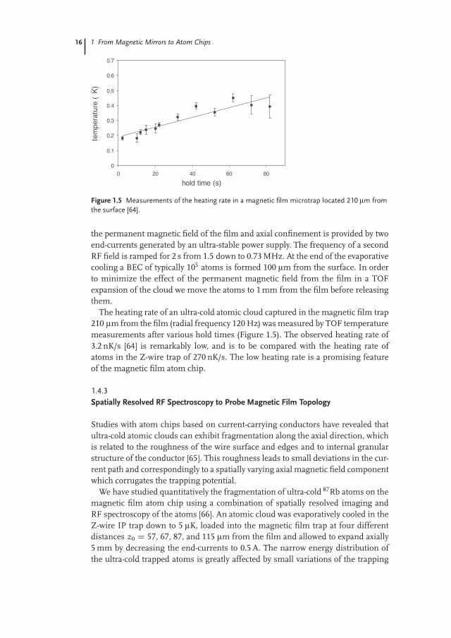
Figure 1.5 Measurements of the heating rate in a magnetic film microtrap located 210 μm fromthe surface [64].
the permanent magnetic field of the film and axial confinement is provided by twoend-currents generated by an ultra-stable power supply. The frequency of a secondRF field is ramped for 2 s from 1.5 down to 0.73 MHz. At the end of the evaporativecooling a BEC of typically 105 atoms is formed 100 μm from the surface. In orderto minimize the effect of the permanent magnetic field from the film in a TOFexpansion of the cloud we move the atoms to 1 mm from the film before releasingthem.
The heating rate of an ultra-cold atomic cloud captured in the magnetic film trap210 μm from the film (radial frequency 120 Hz) was measured by TOF temperaturemeasurements after various hold times (Figure 1.5). The observed heating rate of3.2 nK/s [64] is remarkably low, and is to be compared with the heating rate ofatoms in the Z-wire trap of 270 nK/s. The low heating rate is a promising featureof the magnetic film atom chip.
1.4.3Spatially Resolved RF Spectroscopy to Probe Magnetic Film Topology
Studies with atom chips based on current-carrying conductors have revealed thatultra-cold atomic clouds can exhibit fragmentation along the axial direction, whichis related to the roughness of the wire surface and edges and to internal granularstructure of the conductor [65]. This roughness leads to small deviations in the cur-rent path and correspondingly to a spatially varying axial magnetic field componentwhich corrugates the trapping potential.
We have studied quantitatively the fragmentation of ultra-cold 87Rb atoms on themagnetic film atom chip using a combination of spatially resolved imaging andRF spectroscopy of the atoms [66]. An atomic cloud was evaporatively cooled in theZ-wire IP trap down to 5 μK, loaded into the magnetic film trap at four differentdistances z0 D 57, 67, 87, and 115 μm from the film and allowed to expand axially5 mm by decreasing the end-currents to 0.5 A. The narrow energy distribution ofthe ultra-cold trapped atoms is greatly affected by small variations of the trapping
�
�
Jakob Reichel and Vladan Vuletic: Atom Chips — Chap. reichel7552c01 — 2010/12/2 — page 17 — le-tex
�
�
�
�
�
�
1.4 The Magnetic Film Atom Chip 17
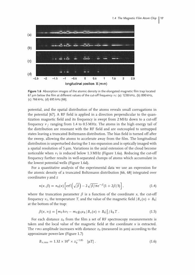
Figure 1.6 Absorption images of the atomic density in the elongated magnetic film trap located67 μm below the film at different values of the cut-off frequency νf : (a) 1238 kHz, (b) 890 kHz,(c) 766 kHz, (d) 695 kHz [66].
potential, and the spatial distribution of the atoms reveals small corrugations inthe potential [67]. A RF field is applied in a direction perpendicular to the quan-tization magnetic field and its frequency is swept from 2 MHz down to a cut-offfrequency ν f ranging from 1.4 to 0.5 MHz. The atoms in the high energy tail ofthe distribution are resonant with the RF field and are outcoupled to untrappedstates leaving a truncated Boltzmann distribution. The bias field is turned off afterthe sweep, allowing the atoms to accelerate away from the film. The longitudinaldistribution is unperturbed during the 1 ms expansion and is optically imaged witha spatial resolution of 5 μm. Variations in the axial extension of the cloud becomenoticeable when νf is reduced below 1.3 MHz (Figure 1.6a). Reducing the cut-offfrequency further results in well-separated clumps of atoms which accumulate inthe lowest potential wells (Figure 1.6d).
For a quantitative analysis of the experimental data we use an expression forthe atomic density of a truncated Boltzmann distribution [66, 68] integrated overcoordinates y and z
n(x , �) D n0(x )herf�p
��� 2
p�/πe��(1C 2�/3)
i, (1.4)
where the truncation parameter � is a function of the coordinate x, the cut-offfrequency νf, the temperature T, and the value of the magnetic field jBx (x )C B0jat the bottom of the trap:
�(x , νf) D�mF hνf � mF gFμB jBx (x )C B0j
�/ kB T . (1.5)
For each distance z0 from the film a set of RF spectroscopy measurements istaken and the local value of the magnetic field at the coordinate x is extracted.The r ms amplitude increases with distance z0 (measured in μm) according to theapproximate power-law (Figure 1.7)
Bx ,rms D 1.32 � 104 � z�1.850 [μT] . (1.6)

�
�
Jakob Reichel and Vladan Vuletic: Atom Chips — Chap. reichel7552c01 — 2010/12/2 — page 18 — le-tex
�
�
�
�
�
�
18 1 From Magnetic Mirrors to Atom Chips
(a)
10
1
0.1
10080604020
Bx,rms,
μT
Bx,rms , n
orm
. uni
ts
Height z, µm–20 –100 0 100 200
0.0
0.2
0.4
0.6
0.8
1.0
(b)Distance y, µm
Figure 1.7 (a) Dependence of the magnetic-field roughness Bx ,rms on height z. The solidline was obtained using Eq. (1.5). (b) De-pendence of the normalized field roughness
predicted by the model (Eq. (1.7)) on thetransverse coordinate y for heights 10 μm(solid), 50 μm (dotted), and 100 μm (dashedline) [66].
Stylus profilometer measurements indicate that the r ms roughness of the pol-ished edge of the slide is around 10 nm over a 400-μm scale. The associated devi-ations of the effective current path cannot explain (i) the large r ms values of thecorrugated axial magnetic field and (ii) the observed z�1.85
0 dependence. When thecloud is positioned z0 D 50 μm below the magnetic surface substantial fragmen-tation is observed. However, when it is positioned 50 μm below the non-magneticgold surface the density distribution exhibits a rather smooth profile. These obser-vations indicate that the random component of the magnetic field originates fromthe bulk of the magnetic film as a result of inhomogeneous magnetization and notfrom variations of the film edge.
We have developed a model [66] to study how the variations in the film mag-netization generate a random magnetic field. For white-noise fluctuations in themagnetization the r ms amplitude of the magnetic noise is
Bx ,rms Dr
3π
μ0 t d0ΔM16z2
r1C 15
8α � 5
4α3 C 3
8α5 , (1.7)
where α D y/p
y 2 C z2, t is the film thickness, d0 is the characteristic feature sizeof the domains, and ΔM is the r ms value of the magnetization variations. Belowthe edge of the film (y D 0) the model predicts that the random magnetic fielddecays with a z�2
0 dependence which is consistent with the observed z�1.85˙0.30 de-
pendence. This is slower than the z�2.50 decay of a corrugated field below current-
carrying microwires [69, 70]. The model predicts an even faster decay of the ran-dom component for y < 0 (Figure 1.7b). Using the experimental r ms values anda characteristic domain size d0 � 5 μm we estimate the level of inhomogeneityΔM/Ms ' 0.3, where Ms is the saturation magnetization of the TbGdFeCo film.If we assume the inhomogeneity originates from reversal of a small number ofdomains and assume a binomial distribution of the reversal then the mean mag-netization is about 0.9Ms.
The observed magnetic inhomogeneity in the TbGdFeCo films is attributed tosome deterioration during vacuum bake-out (140 ıC for 4 days) of the magnetic
�
�
Jakob Reichel and Vladan Vuletic: Atom Chips — Chap. reichel7552c01 — 2010/12/2 — page 19 — le-tex
�
�
�
�
�
�
1.4 The Magnetic Film Atom Chip 19
film atom chip. It was found that such deterioration can be avoided by maintainingthe temperature below 100 ıC.
1.4.4Adiabatic Splitting of a BEC for Asymmetric Potential Sensing
The idea of using adiabatic splitting of a BEC for sensing asymmetric potentials isbased on the assumption that during an adiabatic splitting process the fractionalnumber of atoms in each well of a double-well potential is proportional to the po-tential difference between the bottoms of the wells as long as the chemical potentialis larger than the barrier height [71]. The situation is similar to two coupled poolsof superfluids which have the same level of fluid and the deeper pool will containmore fluid than the shallower pool.
Studies of the magnetic field topology in Section 1.4.3 revealed a double-wellstructure near the center of the film (x � 0, Figure 1.6c,d) with very similar char-acteristics for both wells. One of the features of the random nature of the corrugat-ed magnetic field is that the Fourier components decay exponentially with heightand the short-wavelength components decay much faster than the long-wavelengthcomponents. As a result the barrier between the two wells decreases substantiallywhen the atomic cloud is moved away from the film and the double-well structuremerges into a single well.
Using various values of the bias field an ultra-cold cloud is positioned at differentheights, and the 1D spatial distribution of the atoms is probed by optical imaging.The cloud temperature is measured by TOF expansion. The spatial dependence ofthe trapping potential is determined from the Boltzmann distribution law V(x ) D�kBT ln(n(x )) and the double-well parameters (separation and barrier height) areextracted by fitting the measured potential to a model potential [64]. For a bias fieldof 2.6 G the coalescence point is located 175 μm from the film. Increased values ofthe bias field move the trap closer to the surface and split it into a double well in thelongitudinal (x) direction. The measurements show that the barrier height can beadjusted from sub-kHz up to 100 kHz and the well separation can be up to 180 μm.
Accurate knowledge of the double-well potential was used for precise control ofthe splitting of the BEC. The splitting process and the associated distribution ofatoms between the two wells are extremely sensitive to the presence of any asym-metry component Δ between the bottoms of the two wells [71]. In such a case thenumber of atoms in the deeper well is greater than in the shallower well and isdetermined by the trap frequencies of both wells (by sheer accident these param-eters defined by the corrugated potential are almost identical) as well as externalmagnetic fields or gravity gradients. An asymmetric potential can be either com-pensated or intentionally introduced by applying a current imbalance between theend-wires on the chip (Figure 1.4a). A calibration of the applied potential asym-metry was carried out using RF spectroscopy [71]. Two BECs separated by 170 μmare initially produced in a symmetric double-well potential with a barrier height ofseveral kHz. A large current imbalance of 1 A is introduced in the end-wires for aduration of 500 ms, thereby tilting the wells. A 1-ms RF pulse of variable frequency
�
�
Jakob Reichel and Vladan Vuletic: Atom Chips — Chap. reichel7552c01 — 2010/12/2 — page 20 — le-tex
�
�
�
�
�
�
20 1 From Magnetic Mirrors to Atom Chips
RF frequency (kHz)
outc
oupl
ed fr
actio
n
Δ
Δ
0.0
0.1
0.2
0.3
0.4
0.5
0.6
0.7
775 780 785 790 795
Figure 1.8 Outcoupling of atoms from two condensates in an asymmetric double well as afunction of RF frequency [71].
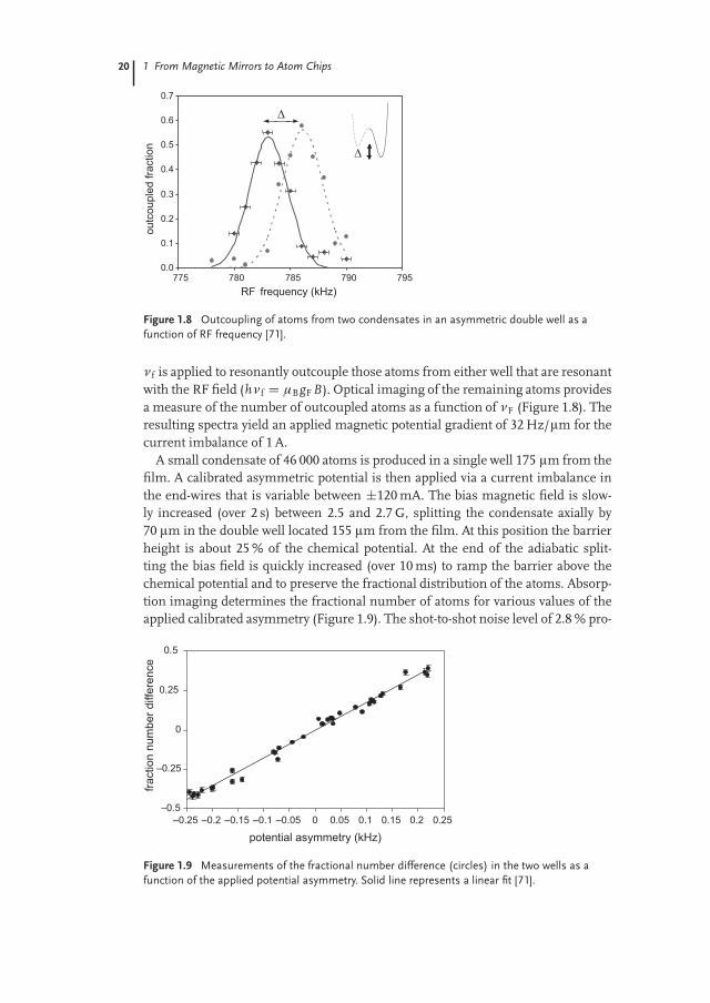
νf is applied to resonantly outcouple those atoms from either well that are resonantwith the RF field (hνf D μBgFB). Optical imaging of the remaining atoms providesa measure of the number of outcoupled atoms as a function of νF (Figure 1.8). Theresulting spectra yield an applied magnetic potential gradient of 32 Hz/μm for thecurrent imbalance of 1 A.
A small condensate of 46 000 atoms is produced in a single well 175 μm from thefilm. A calibrated asymmetric potential is then applied via a current imbalance inthe end-wires that is variable between ˙120 mA. The bias magnetic field is slow-ly increased (over 2 s) between 2.5 and 2.7 G, splitting the condensate axially by70 μm in the double well located 155 μm from the film. At this position the barrierheight is about 25 % of the chemical potential. At the end of the adiabatic split-ting the bias field is quickly increased (over 10 ms) to ramp the barrier above thechemical potential and to preserve the fractional distribution of the atoms. Absorp-tion imaging determines the fractional number of atoms for various values of theapplied calibrated asymmetry (Figure 1.9). The shot-to-shot noise level of 2.8 % pro-
–0.5
–0.25
0
0.25
0.5
–0.25
potential asymmetry (kHz)
fract
ion
num
ber d
iffer
ence
0.250.20.150.10.050–0.05–0.1–0.15–0.2
Figure 1.9 Measurements of the fractional number difference (circles) in the two wells as afunction of the applied potential asymmetry. Solid line represents a linear fit [71].

�
�
Jakob Reichel and Vladan Vuletic: Atom Chips — Chap. reichel7552c01 — 2010/12/2 — page 21 — le-tex
�
�
�
�
�
�
1.4 The Magnetic Film Atom Chip 21
vides a single-shot sensitivity of 17 Hz for the potential well energy imbalance for a70 μm separation. This method of measuring the fractional distribution of atoms issuitable for the construction of sensors of gravitational field gradients. The demon-strated single-shot sensitivity to analogous changes in gravity is δg/g D 2 � 10�4
for a 70 μm separation [71] which corresponds to an 8-nm height difference be-tween the two wells. At present the demonstrated sensitivity to potential gradientsis well below the sensitivity of free-space atom interferometers [72] but surpass-es the sensitivity of on-chip BEC interferometers which are currently limited byrelatively short decoherence times.
1.4.5Spatially Inhomogeneous Phase Evolution of a Two-Component BEC
Accurate knowledge of the phase of matter waves is an important factor in study-ing BEC coherence, and in potential future applications of BEC interferometers.We have studied the relative phase evolution of an elongated two-component BECcomposed of the jF D 1, mF D �1i and jF D 2, mF D 1i hyperfine ground statesof 87Rb atoms [73], magnetically trapped on an atom chip [43]. These two statesare particularly attractive for trapped-atom interferometry because the first-orderZeeman shift between them is canceled at a magnetic field of 3.23 G. To improvethe relative phase detection we developed an imaging technique to simultaneous-ly measure the column density of each hyperfine state during TOF expansion [73].Our dual-state detection produces sub-percent uncertainty in the measured relativepopulation while preserving the spatial mode of each state.
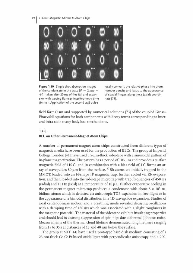
We prepare a condensate in a superposition of the two hyperfine states and in-terrogate the relative phase evolution using two-photon microwave-radiofrequencyRamsey interferometry. The inter- and intra-state scattering lengths have slightlydifferent values and, as a result, the prepared superposition is in a non-equilibriumstate [74], leading to undamped collective oscillations and complex spatial modesof each component. We focus [73] on the dynamics of the relative phase along thedirection of weak (axial) confinement. The relative phase begins (after the first π/2pulse) spatially uniform, then becomes inhomogeneous along the axial coordinate,varying by 1.9π across the condensate after 90 ms of evolution.
The second π/2 pulse converts spatial variations of the relative phase into spatialvariations of the atomic density of each state. The time dependence of the relativephase is accompanied by interference in space and, as a result, spatial fringes ap-pear in the absorption images (Figure 1.10) and change with the evolution time.The spatial dependence of the relative phase leads to inhomogeneous dephasing ofthe condensate wavefunction along the axial direction, and we observe a relativelyfast decay of the Ramsey interference fringes (decay time �70 ms). We emphasizethat, under our conditions, inhomogeneity of the relative phase of the condensatewavefunction is the dominant mechanism for the loss of the Ramsey fringes, ratherthan decoherence due to coupling to the environment or quantum phase diffusion.
Our observations of the spatial evolution of the relative phase and the inhomo-geneous dephasing of the condensate wavefunction are well described by a mean-
�
�
Jakob Reichel and Vladan Vuletic: Atom Chips — Chap. reichel7552c01 — 2010/12/2 — page 22 — le-tex
�
�
�
�
�
�
22 1 From Magnetic Mirrors to Atom Chips
Figure 1.10 Single shot absorption imagesof the condensate in the state jF D 2, mF DC1i taken after 20 ms of free fall and expan-sion with varying Ramsey interferometry time(in ms). Application of the second π/2 pulse
locally converts the relative phase into atomnumber density and leads to the appearanceof spatial fringes along the z (axial) coordi-nate [73].
field formalism and supported by numerical solutions [73] of the coupled Gross–Pitaevskii equations for both components with decay terms corresponding to inter-and intra-state many-body loss mechanisms.
1.4.6BEC on Other Permanent-Magnet Atom Chips
A number of permanent-magnet atom chips constructed from different types ofmagnetic media have been used for the production of BECs. The group at ImperialCollege, London [41] have used 3.5-μm-thick videotape with a sinusoidal pattern ofin-plane magnetization. The pattern has a period of 106 μm and provides a surfacemagnetic field of 110 G, and in combination with a bias field of 1 G forms an ar-ray of waveguides 80 μm from the surface. 87Rb atoms are initially trapped in theMMOT, loaded into an H-shape IP magnetic trap, further cooled via RF evapora-tion, and then loaded into the videotape microtrap with trap frequencies of 450 Hz(radial) and 15 Hz (axial) at a temperature of 10 μK. Further evaporative cooling inthe permanent-magnet microtrap produces a condensate with about 8 � 104 ru-bidium atoms which is detected via anisotropic TOF expansion in free-flight or inthe appearance of a bimodal distribution in a 1D waveguide expansion. Studies ofaxial center-of-mass motion and a breathing mode revealed decaying oscillationswith a damping time of 180 ms which was associated with a slight roughness inthe magnetic potential. The material of the videotape exhibits insulating propertiesand should lead to a strong suppression of spin-flips due to thermal Johnson noise.Measurements of the thermal cloud lifetime demonstrated long lifetimes rangingfrom 15 to 35 s at distances of 15 and 40 μm below the surface.
The group at MIT [44] have used a prototype hard-disk medium consisting of a23-nm-thick Co-Cr-Pt-based oxide layer with perpendicular anisotropy and a 200-
�
�
Jakob Reichel and Vladan Vuletic: Atom Chips — Chap. reichel7552c01 — 2010/12/2 — page 23 — le-tex
�
�
�
�
�
�
1.5 Permanent Magnetic Lattice on a Magnetic Film Atom Chip 23
nm-thick magnetically soft underlayer with a total magnetization of 470 emu/cm3.A pattern with alternating magnetization of period 100 μm was written on the mag-netic substrate. Ultra-cold atoms were loaded into a single microtrap in which axialconfinement was accomplished by a Z-shape wire located below the disk. RF evapo-ration led to the production of 50 000 condensed atoms in the permanent magneticmicrotrap with trap frequencies of 390 Hz (radial) and 9 Hz (axial). Optical imag-ing revealed a bi-modal distribution with a condensate fraction >80 %. A lifetime of�30 s was reported for a height 40 μm above the surface. Tight radial confinementwith a frequency of 16 kHz was demonstrated with a smaller period (10 μm) of thewritten structure. During 1D expansion of the BEC in a waveguide a break-up ofthe atomic cloud was detected at distances closer than 40 μm. This break-up is as-sociated with perturbations of the axial magnetic confinement due to variations inthe magnetic moments of domains and edge-effects during writing of the periodicmagnetic structure.
The group in Amsterdam [45] have constructed a permanent-magnet atomchip consisting of in-plane magnetized 40-μm-thick Fe-Pt foil with a machinedF-shaped self-biased IP trap with frequencies of 11 kHz (axial) and 30 Hz (radial) at180 μm from the surface. The permanent magnetic trap was loaded by transport-ing atoms from a quadrupole magnetic trap by a combination of external magneticfields. RF spectroscopy was employed to analyze the cloud temperature and theatomic distribution in the trap and to observe the onset of Bose condensation insitu without expansion from the trap.
1.5Permanent Magnetic Lattice on a Magnetic Film Atom Chip
1.5.1Background
Optical lattices have been used extensively to manipulate and control periodic ar-rays of ultra-cold atoms and quantum degenerate gases [75], for example, in studiesof low-dimensional quantum gases [76, 77], quantum tunneling experiments suchas the superfluid to Mott insulator quantum phase transition [78] and experimentson BECs in disordered potentials such as Anderson localization [79, 80]. Opticallattices also have potential application in quantum information processing sincethey can provide storage registers for qubits based on neutral atoms [81, 82].
An alternative approach for producing periodic lattices for ultra-cold atoms isbased on periodic arrays of permanent magnetic microstructures on a magneticfilm atom chip [49, 83, 84] using the magnetic micro-structure technology devel-oped for magnetic mirrors [9, 10]. Simple 1D magnetic lattice structures consistingof arrays of 2D traps have been proposed [55, 83] and constructed using current-carrying conductors [85] and video tape [86], though loading of atoms into mul-tiple lattice sites was not demonstrated. 2D lattices of magnetic microtraps withnon-zero potential minima have been proposed based on crossed arrays of current-
�
�
Jakob Reichel and Vladan Vuletic: Atom Chips — Chap. reichel7552c01 — 2010/12/2 — page 24 — le-tex
�
�
�
�
�
�
24 1 From Magnetic Mirrors to Atom Chips
carrying conductors plus bias fields [87, 88] and on crossed arrays of perpendicular-ly magnetized grooved films plus bias fields [83]. Other geometries for constructing2D magnetic lattices have also been proposed, including a single layer of period-ic arrays of square-shaped magnets with three different thicknesses [83, 84] andperiodic arrays of patterned asymmetric Z-shaped structures [46].
Permanent magnetic lattices have some distinctive characteristics. They havehighly stable, reproducible potentials, low technical noise, and extremely low heat-ing rates. They can have large barrier heights and large trap curvature, leading tohigh trap frequencies. They can be constructed with a wide range of periods, downto about 1 μm, and can have tailored complex potentials. They can be readily scaledto have a large number of lattice sites, for example, a 1-μm-period 10 � 10 mm2
2D lattice has 108 sites, which could be very useful as a storage register for quan-tum information processing. They are static and not dynamic; however they can beused in conjunction with current-carrying wire traps to load atoms into the lattice.The atoms need to be prepared in low-field seeking states in order to be trapped,allowing RF evaporative cooling in situ and the use of RF spectroscopy. Finally, per-manent magnetic lattices are suitable for integration onto an atom chip and fordevices. Thus, magnetic lattices may be considered to be complementary to opti-cal lattices, in much the same way as magnetic traps and optical dipole traps arecomplementary.
1.5.2Basic Principles
1.5.2.1 One-Dimensional Magnetic LatticeWe first consider the simple case of a 1D magnetic lattice, similar to the periodicgrooved magnetic mirror described in Section 1.3 but with the addition of biasfields B1x and B1y (Figure 1.11). For an infinite 1D magnetic array with period a,film thickness t and perpendicular magnetization, the components of the magneticfield for distances z � a/4π above the array are given by [83]�
Bx I By I Bz� D hB1x I B0y e�k z sin k y C B1y I B0ye�k z cos k y
i, (1.8)
where k D 2π/a, B0y D B0(1� e�k t)ek t and B0 D 4Mz (Gaussian units).The potential minimum (trap bottom), trap height, barrier heights, and trap fre-
quencies (for a harmonic potential) are given, respectively, by [83]
Bmin D jB1x j , zmin D a2π
ln�
B0y
B1y
�, ΔB y D
�B2
1x C 4B21y
�1/2 � jB1x j ,
ΔB z D�
B21x C B2
1y
�1/2 � jB1x j , ω y D ωz D 2πa
�mFgF μB
M jB1x j�1/2
jB1y j .(1.9)
All of these quantities may be controlled by the bias fields B1x and B1y .Figure 1.11c–e shows numerically calculated contour plots of the magnetic fields
for a finite 1D magnetic lattice and the parameters given in the caption. With no

�
�
Jakob Reichel and Vladan Vuletic: Atom Chips — Chap. reichel7552c01 — 2010/12/2 — page 25 — le-tex
�
�
�
�
�
�
1.5 Permanent Magnetic Lattice on a Magnetic Film Atom Chip 25
(b)(a)
−1 −0.5 0 0.5 10
0.2
0.4
0.6
0.8
1
−1 −0.5 0 0.5 10
0.2
0.4
0.6
0.8
1
−1 −0.5 0 0.5 10
0.2
0.4
0.6
0.8
1
(e)(d)(c)
z (μm
)
z (μm
)
z (μm
)
y (μm) y (μm) y (μm)
B1x B1y y
a/2 a/2
t
z
o
Figure 1.11 (a, b) 1D periodic array of par-allel magnets with perpendicular magnetiza-tion. (c–e) Numerically calculated contourplots of the magnetic field in the central re-gion in the y0z plane with (c) no bias fields,
(d) B1y D �15 G, and (e) B1x D �20 G,B1y D �15 G. 1001 magnets, a D 1 μm,t D 0.05 μm, lx D 1000.5 μm, and4πMz D 3.8 kG [83].
bias fields (Figure 1.11c), the magnitude of the magnetic field falls off exponen-tially with distance z, representing the simple case of a magnetic mirror [9, 10] asdescribed in Section 1.3.1. With the addition of B1y D �15 G (Figure 1.11d), themagnetic field develops 2D magnetic traps with zero potential minima; this config-uration can give rise to spin-flips and is not suitable as a lattice for trapping atoms.With the addition of B1x D �20 G and B1y D �15 G (Figure 1.11e), the magneticfield has 2D magnetic traps with non-zero potential minima, where the trap bottomis given by jB1x j.
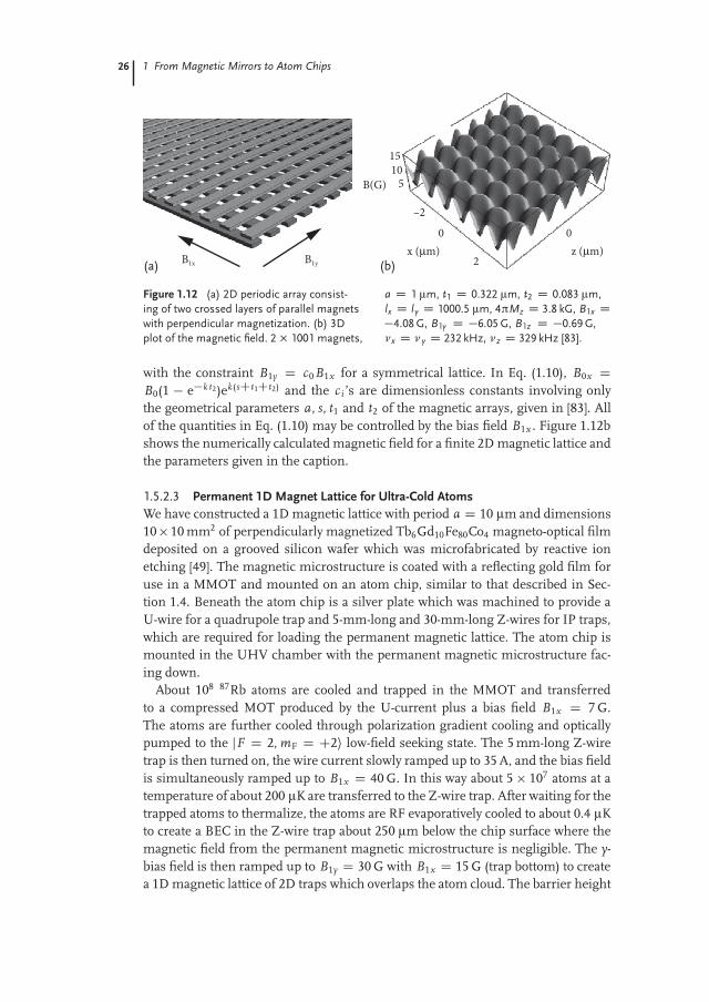
1.5.2.2 Two-Dimensional Magnetic LatticeWe now consider a 2D magnetic lattice produced by two crossed periodic arrays ofparallel magnets, thicknesses t1 and t2, separated by a small distance s (< a/2π),and with bias fields B1x , B1y (Figure 1.12a) [83]. For an infinite symmetrical 2D mag-netic lattice, the trap minimum, trap height, barrier heights, and trap frequencies(for a harmonic potential) are given, respectively, by
Bmin D c1 jB1x j , zmin D a2π
ln�
c2B0x
B1x
�, ΔB x D ΔB y D c4jB1x j ,
ΔB z D c5 jB1x j , ωx D ω y D ωzp2D 2π
a
�mF gFμBc3
M jB1x j�1/2
jB1x j ,(1.10)
�
�
Jakob Reichel and Vladan Vuletic: Atom Chips — Chap. reichel7552c01 — 2010/12/2 — page 26 — le-tex
�
�
�
�
�
�
26 1 From Magnetic Mirrors to Atom Chips
2
–2
0
51015
0
B1y
B(G)
x (μm) z (μm)B1x(a) (b)
Figure 1.12 (a) 2D periodic array consist-ing of two crossed layers of parallel magnetswith perpendicular magnetization. (b) 3Dplot of the magnetic field. 2 � 1001 magnets,
a D 1 μm, t1 D 0.322 μm, t2 D 0.083 μm,lx D ly D 1000.5 μm, 4πMz D 3.8 kG, B1x D�4.08 G, B1y D �6.05 G, B1z D �0.69 G,νx D ν y D 232 kHz, νz D 329 kHz [83].
with the constraint B1y D c0B1x for a symmetrical lattice. In Eq. (1.10), B0x DB0(1 � e�k t2)ek(sCt1Ct2) and the c i ’s are dimensionless constants involving onlythe geometrical parameters a, s, t1 and t2 of the magnetic arrays, given in [83]. Allof the quantities in Eq. (1.10) may be controlled by the bias field B1x . Figure 1.12bshows the numerically calculated magnetic field for a finite 2D magnetic lattice andthe parameters given in the caption.
1.5.2.3 Permanent 1D Magnet Lattice for Ultra-Cold AtomsWe have constructed a 1D magnetic lattice with period a D 10 μm and dimensions10� 10 mm2 of perpendicularly magnetized Tb6Gd10Fe80Co4 magneto-optical filmdeposited on a grooved silicon wafer which was microfabricated by reactive ionetching [49]. The magnetic microstructure is coated with a reflecting gold film foruse in a MMOT and mounted on an atom chip, similar to that described in Sec-tion 1.4. Beneath the atom chip is a silver plate which was machined to provide aU-wire for a quadrupole trap and 5-mm-long and 30-mm-long Z-wires for IP traps,which are required for loading the permanent magnetic lattice. The atom chip ismounted in the UHV chamber with the permanent magnetic microstructure fac-ing down.
About 108 87Rb atoms are cooled and trapped in the MMOT and transferredto a compressed MOT produced by the U-current plus a bias field B1x D 7 G.The atoms are further cooled through polarization gradient cooling and opticallypumped to the jF D 2, mF D C2i low-field seeking state. The 5 mm-long Z-wiretrap is then turned on, the wire current slowly ramped up to 35 A, and the bias fieldis simultaneously ramped up to B1x D 40 G. In this way about 5 � 107 atoms at atemperature of about 200 μK are transferred to the Z-wire trap. After waiting for thetrapped atoms to thermalize, the atoms are RF evaporatively cooled to about 0.4 μKto create a BEC in the Z-wire trap about 250 μm below the chip surface where themagnetic field from the permanent magnetic microstructure is negligible. The y-bias field is then ramped up to B1y D 30 G with B1x D 15 G (trap bottom) to createa 1D magnetic lattice of 2D traps which overlaps the atom cloud. The barrier height
�
�
Jakob Reichel and Vladan Vuletic: Atom Chips — Chap. reichel7552c01 — 2010/12/2 — page 27 — le-tex
�
�
�
�
�
�
1.5 Permanent Magnetic Lattice on a Magnetic Film Atom Chip 27
(i)
(ii)
(a) (b)
Figure 1.13 (a) Absorption image of atoms re-leased from the magnetic lattice after (i) 4 msand (ii) 16 ms time of flight. The broken struc-ture in (i) is due to non-uniform reflection ofthe imaging beam from the grooved structure;
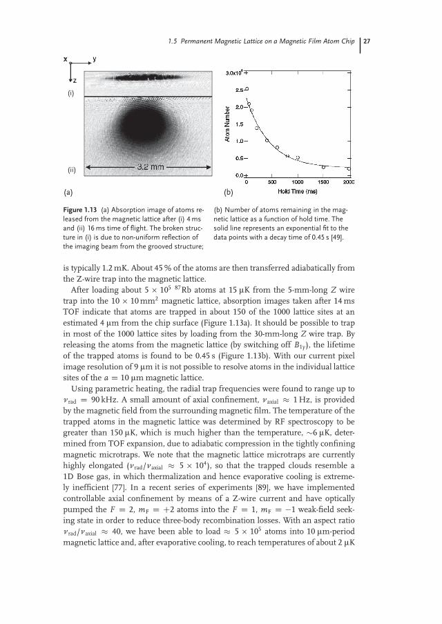
(b) Number of atoms remaining in the mag-netic lattice as a function of hold time. Thesolid line represents an exponential fit to thedata points with a decay time of 0.45 s [49].
is typically 1.2 mK. About 45 % of the atoms are then transferred adiabatically fromthe Z-wire trap into the magnetic lattice.
After loading about 5 � 105 87Rb atoms at 15 μK from the 5-mm-long Z wiretrap into the 10 � 10 mm2 magnetic lattice, absorption images taken after 14 msTOF indicate that atoms are trapped in about 150 of the 1000 lattice sites at anestimated 4 μm from the chip surface (Figure 1.13a). It should be possible to trapin most of the 1000 lattice sites by loading from the 30-mm-long Z wire trap. Byreleasing the atoms from the magnetic lattice (by switching off B1y ), the lifetimeof the trapped atoms is found to be 0.45 s (Figure 1.13b). With our current pixelimage resolution of 9 μm it is not possible to resolve atoms in the individual latticesites of the a D 10 μm magnetic lattice.
Using parametric heating, the radial trap frequencies were found to range up toνrad D 90 kHz. A small amount of axial confinement, νaxial � 1 Hz, is providedby the magnetic field from the surrounding magnetic film. The temperature of thetrapped atoms in the magnetic lattice was determined by RF spectroscopy to begreater than 150 μK, which is much higher than the temperature, �6 μK, deter-mined from TOF expansion, due to adiabatic compression in the tightly confiningmagnetic microtraps. We note that the magnetic lattice microtraps are currentlyhighly elongated (νrad/νaxial � 5 � 104), so that the trapped clouds resemble a1D Bose gas, in which thermalization and hence evaporative cooling is extreme-ly inefficient [77]. In a recent series of experiments [89], we have implementedcontrollable axial confinement by means of a Z-wire current and have opticallypumped the F D 2, mF D C2 atoms into the F D 1, mF D �1 weak-field seek-ing state in order to reduce three-body recombination losses. With an aspect ratioνrad/νaxial � 40, we have been able to load � 5 � 105 atoms into 10 μm-periodmagnetic lattice and, after evaporative cooling, to reach temperatures of about 2 μK

�
�
Jakob Reichel and Vladan Vuletic: Atom Chips — Chap. reichel7552c01 — 2010/12/2 — page 28 — le-tex
�
�
�
�
�
�
28 1 From Magnetic Mirrors to Atom Chips
with a trap lifetime of�10 s. This should allow us to reach quantum degeneracy inthe individual magnetic lattice sites and to generate multiply arrays of condensates.
In order to perform quantum tunneling experiments in the magnetic lattice itwill be necessary to reduce the lattice period down to a � 2�4 μm.
1.5.2.4 Other Permanent Magnetic LatticesThe group in Amsterdam [47] have recently realized a 2D array of microtraps abovemultiple Z-shaped patterns microfabricated in a 300-nm-thick Fe-Pt film (Mr D670 kA/m). The magnetic lattice of ultra-cold 87Rb F D 2, mF D 1 atoms (periods22 μm and 36 μm in orthogonal directions) was produced 10 μm above the surfacewith very tight confinement (radial and axial frequency 13.4 kHz). Atoms from amacroscopic Z-wire trap were loaded into more than 500 traps and individual trapswere optically resolved. Three-body recombination losses were used to characterizethe number and temperature of the atoms in the individual traps and show theonset of BEC in 70 sites. However, the average condensate fraction is less than0.1 which is attributed to the very tight confinement. Transport of the atoms overseveral lattice sites in one direction and back was demonstrated. A focused laserbeam was used to empty one site and move it over several periods. These studiesare promising for building a scalable quantum information processor based onneutral-atom permanent-magnet chips.
1.6Summary and Conclusions
After almost two decades since the initial ideas of surface-based magnetic opticalelements for ultra-cold atoms were proposed, the use of atom chips for produc-ing and manipulating clouds of ultra-cold atoms and quantum degenerate gaseson a substrate has evolved into a very active new area of research. Atom chips al-low the construction and integration of miniature networks of magnetic micro-traps, waveguides, and interferometers into a single device. The combination ofpermanent magnetic materials with dynamic current-carrying conductors to pro-duce complex magnetic field configurations offers a promising way of construct-ing stable low-noise atom chips with micron-scale elements. Such devices have awealth of potential future applications as trapped-atom interferometers, sensorsof potential gradients, chip-based atomic clocks, microsensors of magnetic fieldtopology and storage registers for quantum information processing.
Acknowledgments
The authors thank the many colleagues who have contributed to the work reportedin this article, including Alexander Akulshin, Russell Anderson, Tim Davis, SaeedGhanbari, David Gough, Brenton Hall, Smitha Jose, Tien Kieu, Leszek Krzemien,
�
�
Jakob Reichel and Vladan Vuletic: Atom Chips — Chap. reichel7552c01 — 2010/12/2 — page 29 — le-tex
�
�
�
�
�
�
1.6 Summary and Conclusions 29
David Lau, Russell McLean, Geoffrey Opat, Timothy Roach, Wayne Rowlands, FalkScharnberg, Mandip Singh, Chris Ticknor, Michael Volk, James Wang, and Shan-non Whitlock. The work is supported by the Australian Research Council.
References
1 Opat, G.I. (1983) In Proc. 3rd MarcelGrossmann Meeting of General Relativi-ty, Part B (ed. Hu Ning), Beijing, Sci-ence press, Amsterdam, North Holland,p 1491.
2 Wark, S. and Opat, G.I. (1992) J. Phys. B25, 4229.
3 Opat, G.I., Wark, S.J., and Cimmino, A.(1992) Appl. Phys. B 54, 396.
4 Roach, T.M., Abele, H., Boshier, M.G.,Grossman, H.L., Zetie, K.P., and Hinds,E.A. (1995) Phys. Rev. Lett. 75, 629.
5 Sidorov, A.I., McLean, R.J., Row-lands, W.J., Lau, D.C., Murphy, J.E.,Walkiewicz, M., Opat, G.I., and Han-naford, P. (1996) Quant. Semiclass. Opt.8, 713.
6 Hughes, I.G., Barton, P.A., Roach, T.M.,Boshier, M.G., and Hinds, E.A. (1997)J. Phys. B 30, 647.
7 Saba, C.V., Barton, P.A., Boshier,M.G., Hughes, I.G., Rosenbusch, P.,Sauer, B.E., and Hinds, E.A. (1999)Phys. Rev. Lett. 82, 468.
8 Sidorov, A.I., Lau, D.C., Opat, G.I.,McLean, R.J., Rowlands, W.J., and Han-naford, P. (1998) Laser Physics 8, 642.
9 Sidorov, A.I., McLean, R.J., Sexton, B.A.,Gough, D.S., Davis, T.J., Akulshin, A.,Opat, G.I., and Hannaford, P. (2001)Compt. Rendus 2(4), 565.
10 Sidorov, A.I., McLean, R.J., Scharnberg,F., Gough, D.S., Davis, T.J., Sexton, B.J.,Opat, G.I., and Hannaford, P. (2002)Acta Phys. Polon. B 33, 2137.
11 Lau, D.C., Sidorov, A.I., Opat, G.I.,McLean, R.J., Rowlands, W.J., and Han-naford, P. (1999) Eur. J. Phys. D 5, 193.
12 Drndic, M., Zabow, G., Lee, C.S., Thy-wissen, J.H., Johnson, K.S., Prentiss,M., Westervelt, R.M., Featonby, P.D.,Savalli, V., Cognet, L., Helmerson, K.,Westbrook, N., Westbrook, C.I., Phillips,W.D., and Aspect, A. (1999) Phys. Rev. A60, 4012.
13 Folman, R., Krüger, P., Schmiedmayer,J., Denschlag, J., and Henkel, C. (2002)Adv. At., Mol. Opt. Phys. 48, 263.
14 Reichel, J. (2002) Appl. Phys. B 75, 469.15 Fortágh, J. and Zimmermann, C. (2007)
Rev. Mod. Phys. 79, 235.16 Weinstein, J.D. and Libbrecht, K.G.
(1995) Phys. Rev. A 52, 4004.17 Vuletic, V., Fischer, T., Praeger, M., Hän-
sch, T.W., and Zimmermann, C. (1998)Phys. Rev. Lett. 80, 1634.
18 Fortágh, J., Grossmann, A., Zimmer-mann, C. and Hänsch, T.W. (1998)Phys. Rev. Lett. 81, 5310.
19 Drndic, M., Johnson, K.S., Thywissen,J.H., Prentiss, M., and Westervelt, R.M.(1998) Appl. Phys. Lett. 72, 2906.
20 Reichel, J., Hänsel, W., and Hänsch,T.W. (1999) Phys. Rev. Lett. 83, 3398.
21 Denschlag, J., Cassettari, D., andSchmiedmayer, J. (1999) Phys. Rev. Lett.82, 2014.
22 Müller, D., Anderson, D.Z., Grow, R.J.,Schwindt, P.D.D., and Cornell, E.A.(1999) Phys. Rev. Lett. 83, 5194.
23 Dekker, N.H., Lee, C.S., Lorent, V.,Thywissen, J.H., Smith, S.P., Drndic,M., Westervelt, R.M., and Prentiss, M.(2000) Phys. Rev. Lett. 84, 1124.
24 Key, M., Hughes, I.G., Rooijakkers,W., Sauer, B.E., Hinds, E.A., Richard-son, D.J., and Kazansky, P.G. (2000)Phys. Rev. Lett. 84, 1371.
25 Davis, T.J. (1999) J. Phys. B: Quant.Semicl. Opt. 1, 408.
26 Folman, R., Krüger, P., Cassettari, D.,Hessmo, B., Maier, T., and Schmiedmay-er, J. (2000) Phys. Rev. Lett. 84, 4749.
27 Hänsel, W., Reichel, J., Hommelhoff, P.,and Hänsch, T.W. (2001) Phys. Rev. Lett.86, 608.
28 Hänsel, W., Hommelhoff, P., Hänsch,T.W., and Reichel, J. (2001) Nature 413,498.
�
�
Jakob Reichel and Vladan Vuletic: Atom Chips — Chap. reichel7552c01 — 2010/12/2 — page 30 — le-tex
�
�
�
�
�
�
30 1 From Magnetic Mirrors to Atom Chips
29 Ott, H., Fortágh, J., Schlotterbeck, G.,Grossmann, A., and Zimmermann, C.(2001) Phys. Rev. Lett. 87, 230401.
30 Aubin, S., Myrskog, S., Extavour, M.H.T.,LeBlanc, L.J., McKay, D., Stummer, A.,and Thywissen, J.H. (2006) Nature Phys.2, 384.
31 Treutlein, P., Hommelhoff, P., Stein-metz, T., Hänsch, T.W., and Reichel, J.(2004) Phys. Rev. Lett. 92, 203005.
32 Knappe, S., Shah, V., Schwindt, P.D.D.,Hollberg, L., Kitching, J., Liew, L.-A.,and Moreland, J. (2004) Appl. Phys. Lett.85, 1460.
33 Shin, Y., Sanner, C., Jo, G.-B., Pasquini,T.A., Saba, M., Ketterle, W., Pritchard,D.E., Vengalattore, M. and Prentiss, M.(2005) Phys. Rev. A 72, 021604.
34 Schumm, T., Hofferberth, S., Anders-son, L.M., Wildermuth, S., Groth, S.,Bar-Joseph, I., Schmiedmayer, J., andKrüger, P. (2005) Nature Phys. 1, 57.
35 Wang, Y.-J., Anderson, D.Z., Bright,V.M., Cornell, E.A., Diot, Q., Kishimo-to, T., Prentiss, M., Saravanan, R.A.,Segal, S.R., and Saijun, W. (2005)Phys. Rev. Lett. 94, 090405.
36 Jo, G.-B., Shin, Y., Will, S., Pasquini,T.A., Saba, M., Ketterle, W., Pritchard,D.E., Vengalattore, M., and Prentiss, M.(2007) Phys. Rev. Lett. 98, 030407.
37 Böhi, P., Riedel, M.F., Hoffrogge, J.,Reichel, J., Hänsch, T.W., and Treutlein,P. (2009) Nature Phys. 5, 592.
38 Riedel, M.F., Böhl, P., Li, Y., Hänsch,T.W., Sinatra, A., and Treutlin, P. (2010)Nature 464, 1170.
39 Deutsch, C. Ramirez-Martinez, F.,Lacroûte, C., Reinhard, F., Schneider,T., Fuchs, J.N., Piéchon, F., Laloë, F.,Reichel, J., and Rosenbusch, P. (2010)Phys. Rev. Lett. 105, 020401.
40 Lhuiller, C. and Laloë, F. (1982)J. Phys. (Paris) 43, 197 and 225.
41 Sinclair, C.D.J., Curtis, E.A., LlorenteGarcia, I., Retter, J.A., Hall, B.V., Eriks-son, S., Sauer, B.E., and Hinds, E.A.(2005) Phys. Rev. A 72, 031603.
42 Hall, B.V., Whitlock, S., Scharnberg, F.,Hannaford, P., and Sidorov, A. (2005)Laser Spectroscopy 17, (eds E.A. Hinds, A.Ferguson, and E. Riis), World Scientific,Singapore, p. 275.
43 Hall, B.V., Whitlock, S., Scharnberg, F.,Hannaford, P., and Sidorov, A. (2006)J. Phys. B 39, 27.
44 Boyd, M., Streed, E.W., Medley, P.,Campbell, G.K., Mun, J., Ketterle, W.,and Pritchard, D.E. (2007) Phys. Rev. A76, 043624.
45 Fernholz, T., Gerritsma, R., Whitlock,S., Barb, I., and Spreeuw, R.J.C. (2008)Phys. Rev. A 77, 033409.
46 Gerritsma, R., Whitlock, S., Fernholz,T., Schlatter, H., Luigjes, J.A., Thiele, J.-U., Goedkoop, J.B., and Spreeuw, R.J.C.(2007) Phys. Rev. A 76, 033408.
47 Whitlock, S., Fernholz, T., Gerritsma, R.,Schlatter, H., Luigjes, J.A., Thiele, J.-U.,Goedkoop, J.B., and Spreeuw, R.J.C.(2009) New J. Phys. 11, 023021.
48 Singh, M., Whitlock, S., Anderson, R.,Ghanbari, S., Hall, B.V., Volk, M., Akul-shin, A., McLean, R., Sidorov, A., andHannaford, P. (2008) Laser Spectroscopy18 (eds J. Bergquist, L. Hollberg, and M.Kasevich), New York, World Scientific,p. 228.
49 Singh, M., Volk, M., Akulshin, A.,Sidorov, A., McLean, R., and Hannaford,P. (2008) J. Phys. B 41, 065301.
50 Nirrengarten, T., Qarry, A., Roux, C.,Emmert, A., Nogues, G., Brune, M.,Raimond, J.-M., and Haroche, S. (2006)Phys. Rev. Lett. 97, 200405.
51 Mukai, T., Hufnagel, C., Kasper, A.,Meno, T., Tsukada, A., Semba, K., andShimizu, F. (2007) Phys. Rev. Lett. 98,260407.
52 Roux, C., Emmert, A., Lupascu, A., Nir-rengarten, T., Nogues, G., Brune, M.,Raimond, J.-M., and Haroche, S. (2008)Eur. Phys. Lett. 81, 56004.
53 Cano, D., Kasch, B., Hattermann, H.,Kleiner, R., Zimmermann, C., Koelle,D., and Fortágh, J. (2008) Phys. Rev. Lett.101, 183006.
54 Singh, M. (2009) Opt. Express 17, 2600.55 Hinds, E.A. and Hughes, I.G. (1999)
J. Phys. D 32, R119.56 Lau, D.C., McLean, R.J., Sidorov, A.I.,
Gough, D.S., Koperski, J., Rowlands,W.J., Sexton, B.A., Opat, G.I., and Han-naford, P. (1999) J. Opt. B 1, 371.
57 Davis, T.J. (2001) Eur. J. Phys. D 14, 111.
�
�
Jakob Reichel and Vladan Vuletic: Atom Chips — Chap. reichel7552c01 — 2010/12/2 — page 31 — le-tex
�
�
�
�
�
�
1.6 Summary and Conclusions 31
58 Opat, G.I., Nic Chormaic, S., Cantwell,B.P., and Richmond, J.A. (2004) J. Opt. B1, 415 (1999).
59 Wang, J.Y., Whitlock, S., Scharnberg, F.,Gough, D.S., Sidorov, A.I., McLean, R.J.,and Hannaford, P. (2005) J. Phys. D 38,4015.
60 Hinds, E.A., Boshier, M.G., and Hughes,I.G. (1998) Phys. Rev. Lett. 80, 645.
61 Eriksson, S., Ramirez-Martinez, F.,Curtis, E.A., Sauer, B.E., Nutter, P.W.,Hill, E.W., and Hinds, E.A. (2004) Ap-pl. Phys. B 79, 811.
62 Krüger, P., Luo, X., Klein, M.W., Brug-ger, K., Haase, A., Wildermuth, S.,Groth, S., Bar-Joseph, I., Folman, R., andSchmiedmayer, J. (2003) Phys. Rev. Lett.91, 233201.
63 Henkel, C., Pötting, S., and Wilkins, M.(1999) Appl. Phys. B 69, 379.
64 Whitlock, S. (2007) Bose–Einstein con-densates on a magnetic film atom chipPhD thesis, Swinburne University ofTechnology, p. 92.
65 Fortágh, J., Ott, H., Kraft, S., Gün-ther, A., and Zimmermann, C. (2002)Phys. Rev. A 66, 041604.
66 Whitlock, S., Hall, B.V., Roach, T., An-derson, R., Volk, M., Hannaford, P.,and Sidorov, A. (2007) Phys. Rev. A 75,043602.
67 Wildermuth, S., Hofferberth, S.,Lesanovsky, I., Haller, E., Andersson,L.M., Groth, S., Bar-Joseph, I., Krüger,P., and Schmiedmayer, J. (2005) Nature435, 440.
68 Luiten, O.J., Reynolds, M.W., and Wal-raven, J.T.M. (1996) Phys. Rev. A 53,381.
69 Wang, D.W., Lukin, M.D., and Demler,E. (2004) Phys. Rev. Lett. 92, 076802.
70 Estéve, J., Aussibal, C., Schumm, T., Figl,C., Mailly, D., Bouchoule, I., Westbrook,C.I., and Aspect, A. (2004) Phys. Rev. A70, 043629.
71 Hall, B.V., Whitlock, S., Anderson, R.,Hannaford, P., and Sidorov, A. (2007)Phys. Rev. Lett. 98, 030402.
72 McGuirk, J.M., Foster, G.T., Fixler, J.B.,Snaddon, M.J., and Kasevich, M.A.(2002) Phys. Rev. A 65, 033608.
73 Anderson, R.P., Ticknor, C., Sidorov,A.I., and Hall, B.V. (2009) Phys. Rev. A80, 023603.
74 Mertes, K.M., Merrill, J.W., Carretero-Gonzáles, R., Frantzeskakis, D.J.,Kevrekidis, P.G., and Hall, D.S. (2007)Phys. Rev. Lett. 99, 190402.
75 For example, Bloch, I. (2004)Physics World 98(4), 25.
76 Tolra Laburthe, B., O’Hara, K.M., Huck-ans, J.H., Phillips, W.D., Rolston, S.L.,and Porto, J.V. (2004) Phys. Rev. Lett. 92,19040.
77 Kinoshita, T., Wenger, T., and Weiss,D.S. (2006) Nature 440, 900.
78 Greiner, M., Mandel, O., Esslinger, T.,Hänsch, T., and Bloch, I. (2002) Nature415, 39.
79 Billy, J., Josse, V., Zuo, Z., Bernard, A.,Hambrecht, B., Lugan, P., Clement, D.,Sanchez-Palencia, L., Bouyer, P., andAspect, A. (2008) Nature 453, 891.
80 Roati, G., D’Errico, C., Fallani, L., Fattori,M., Fort, C., Zaccanti, M., Modugno, G.,Modugno, M., and Inguscio, M. (2008)Nature 453, 895.
81 Calarco, T., Hinds, E.A., Jaksch, D.,Schmiedmayer, J., Cirac, J.I., and Zoller,P. (2000) Phys. Rev. A 61, 022304.
82 Schrader, D., Dotsenko, I., Khu-daverdyan, M., Miroshnychenko, Y.,Rauschenbeutal, A., and Meschede, D.(2004) Phys. Rev. Lett. 93, 150501.
83 Ghanbari, S., Kieu, T.D., Sidorov, A., andHannaford, P. (2006) J. Phys. B 39, 847.
84 Ghanbari, S., Kieu, T.D., and Hannaford,P. (2007) J. Phys. B 40, 1283.
85 Günther, A., Kemmler, M., Kraft, S.,Vale, C.J., Zimmermann, C., andFortágh, J. (2005) Phys. Rev. A 71,063619.
86 Sinclair, D.J., Retter, J.A., Curtis, E.A.,Hall, B.V., Llorente Garcia, I., Eriksson,S., Sauer, B.E., and Hinds, E.A. (2005)Eur. Phys. J. 35, 105.
87 Yin, J., Gao, W., Hu, J., and Wang, Y.(2002) Opt. Commun. 206, 99.
88 Grabowski, A. and Pfau, T. (2003)Eur. Phys. J. D 22, 347.
89 Jose, S., Krzemien, L., Withlock, S.,Singh, M., Sidorov, A., McLean, R., andHannaford, P. In preparation.

�
�
Jakob Reichel and Vladan Vuletic: Atom Chips — Chap. reichel7552c02 — 2010/12/2 — page 32 — le-tex
�
�
�
�
�
�