Embed Size (px)
Citation preview
Fulvio TESSAROTTO RD51 meeting, Paris, 14/10/2008 THGEM production at ELTOSRD51 meeting, Paris, 14/10/2008 THGEM production at ELTOS 11
Production of THGEM at ELTOS Production of THGEM at ELTOS S.p.A.S.p.A.
Company profile
Production procedures
Small size THGEM prototypes
Large area THGEM photon detector
The production of the first set of 600 x 600 mm2 THGEM prototypes
Fulvio Tessarotto

Fulvio TESSAROTTO RD51 meeting, Paris, 14/10/2008 THGEM production at ELTOSRD51 meeting, Paris, 14/10/2008 THGEM production at ELTOS 22
Company profile (seen from a Company profile (seen from a client)client)
For the production of THGEMs by industry Rui de Oliveira suggested
us to contact an Italian pcb producer: the company ELTOS S.p.A.
Founded in 1980 by Dr. Riccardo Pinamonti, in Arezzo (Tuscany),
a place with centuries long tradition in gold handcraft
almost 100 workers; turnover > 12 M€ / year; page: www.eltos.it
producing of all kinds of pcb’s, mainly for foreign customers
many labs and research institutes among clients (CERN LHCb award)
typically working on special products and small orders
treating more than 30 different codes / day
using many high-tech machines and newly developed techniques
Fulvio TESSAROTTO RD51 meeting, Paris, 14/10/2008 THGEM production at ELTOSRD51 meeting, Paris, 14/10/2008 THGEM production at ELTOS 33
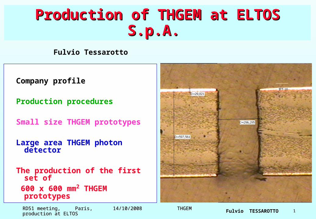
Production of small size THGEM Production of small size THGEM prototypesprototypes
At the beginning of 2008 we ordered to the ELTOS Company 13 groups of THGEM
prototypes with 30 x 30 mm2 of active area.
POSALUX ULTRASPEED 6000LZ6-spindle-roboter
180,000 turns/min, Ø down to 0.15 mmNominal CNC drilling tolerance: +- 10 μm
common prototype parameters:thickness: 0.4 mm,Cu thickness: 35 μm, holes diameter: 0.4 mm,pitch: 0.8 mm;material: R-1566 Panasonic (halogen free, anti CAF)
10 samples per type
Fulvio TESSAROTTO RD51 meeting, Paris, 14/10/2008 THGEM production at ELTOSRD51 meeting, Paris, 14/10/2008 THGEM production at ELTOS 44
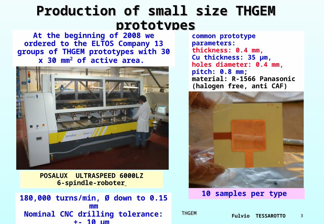
13 series (different rim or 13 series (different rim or production)production)
NameDrilling 0.4
mm Rim 1 (μm) Rim 2 (μm) rim production material
M1 Y 0 0 NO Panasonic
M2 Y 25 0 Drilling Panasonic
M3 Y 50 0 Drilling Panasonic
M4 Y 100 0 Drilling Panasonic
M5 Y 50 50 Two Sides Drilling Panasonic
R NO NO NO NO Panasonic
RI NO NO NO NO Isola
C1 Y 10 10 Etching Panasonic
C2 Y 25 25 Etching Panasonic
C3 Y 50 50 Etching Panasonic
C3I Y 50 50 Etching Isola
C4 Y 100 100 Etching Panasonic
C5 Y 10 10 Laser + Etching Panasonic
C6 Y 50 50 Laser + Etching Panasonic
C7 Y 10 10 Global Etching Panasonic
Fulvio TESSAROTTO RD51 meeting, Paris, 14/10/2008 THGEM production at ELTOSRD51 meeting, Paris, 14/10/2008 THGEM production at ELTOS 55
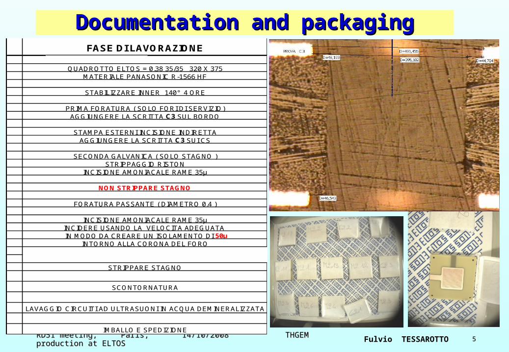
Documentation and packagingDocumentation and packagingFASE DI LAVORAZIONE
QUADROTTO ELTOS = 0.38 35/35 320 X 375MATERIALE PANASONIC R-1566 HF
STABILIZZARE INNER 140° 4 ORE
PRIMA FORATURA ( SOLO FORI DI SERVIZIO)AGGIUNGERE LA SCRITTA C3 SUL BORDO
STAMPA ESTERNI INCISIONE INDIRETTAAGGIUNGERE LA SCRITTA C3 SUI CS
SECONDA GALVANICA ( SOLO STAGNO )STRIPPAGGIO RISTON
INCISIONE AMONIACALE RAME 35µ
NON STRIPPARE STAGNO
FORATURA PASSANTE ( DIAMETRO 0.4 )
INCISIONE AMONIACALE RAME 35µINCIDERE USANDO LA VELOCITA ADEGUATA IN MODO DA CREARE UN ISOLAMENTO DI 50µ
INTORNO ALLA CORONA DEL FORO
STRIPPARE STAGNO
SCONTORNATURA
LAVAGGIO CIRCUITI AD ULTRASUONI IN ACQUA DEMINERALIZZATA
IMBALLO E SPEDIZIONE
Fulvio TESSAROTTO RD51 meeting, Paris, 14/10/2008 THGEM production at ELTOSRD51 meeting, Paris, 14/10/2008 THGEM production at ELTOS 66
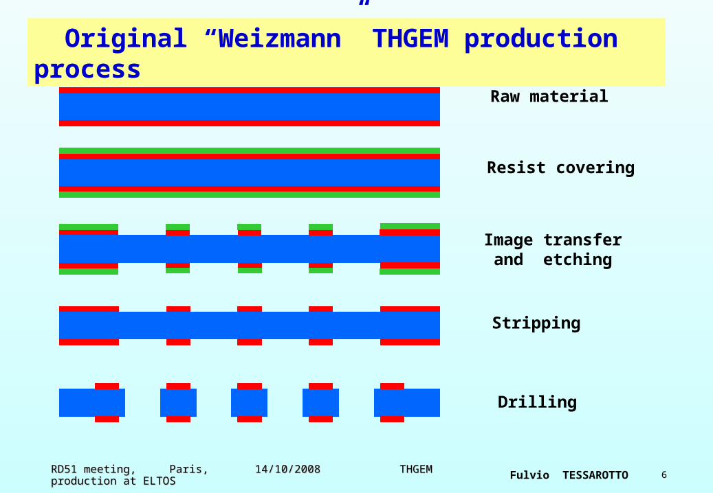
Raw material
Image transfer and etching
Drilling
Stripping
Resist covering
Original “Weizmann” THGEM production process
Fulvio TESSAROTTO RD51 meeting, Paris, 14/10/2008 THGEM production at ELTOSRD51 meeting, Paris, 14/10/2008 THGEM production at ELTOS 77
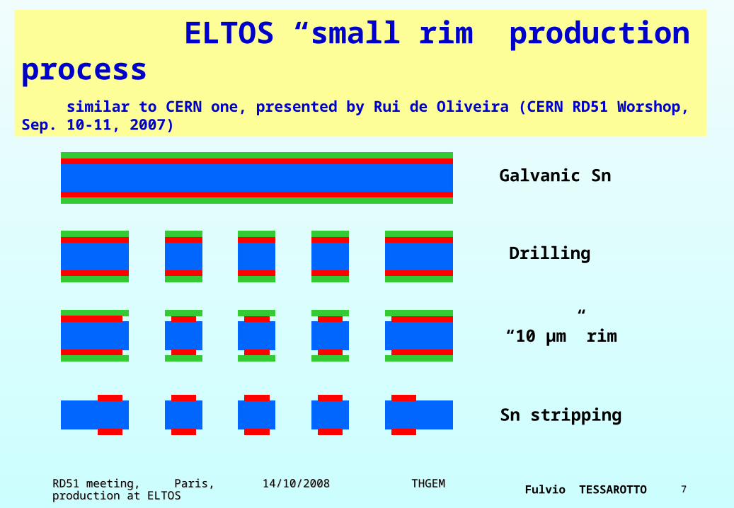
Raw material
Drilling
Sn stripping
“10 μm” rim
Galvanic Sn
ELTOS “small rim” production process similar to CERN one, presented by Rui de Oliveira (CERN RD51 Worshop, Sep. 10-11, 2007)
Fulvio TESSAROTTO RD51 meeting, Paris, 14/10/2008 THGEM production at ELTOSRD51 meeting, Paris, 14/10/2008 THGEM production at ELTOS 88
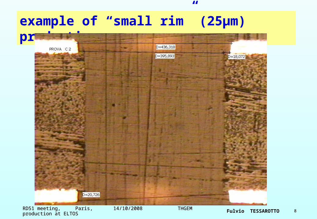
example of “small rim” (25μm) production
Fulvio TESSAROTTO RD51 meeting, Paris, 14/10/2008 THGEM production at ELTOSRD51 meeting, Paris, 14/10/2008 THGEM production at ELTOS 99
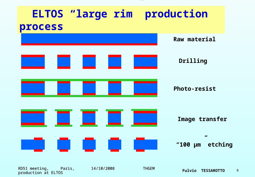
Raw material
Photo-resist
“100 μm” etching
Image transfer
Drilling
ELTOS “large rim” production process
Fulvio TESSAROTTO RD51 meeting, Paris, 14/10/2008 THGEM production at ELTOSRD51 meeting, Paris, 14/10/2008 THGEM production at ELTOS 1010
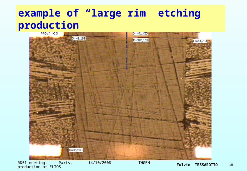
example of “large rim” etching production
Fulvio TESSAROTTO RD51 meeting, Paris, 14/10/2008 THGEM production at ELTOSRD51 meeting, Paris, 14/10/2008 THGEM production at ELTOS 1111
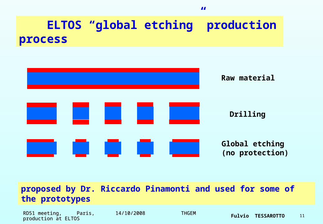
Raw material
Drilling
Global etching (no protection)
ELTOS “global etching” production process
proposed by Dr. Riccardo Pinamonti and used for some of the prototypes

Fulvio TESSAROTTO RD51 meeting, Paris, 14/10/2008 THGEM production at ELTOSRD51 meeting, Paris, 14/10/2008 THGEM production at ELTOS 1212
example of 10 μm “global etching” production
Fulvio TESSAROTTO RD51 meeting, Paris, 14/10/2008 THGEM production at ELTOSRD51 meeting, Paris, 14/10/2008 THGEM production at ELTOS 1313
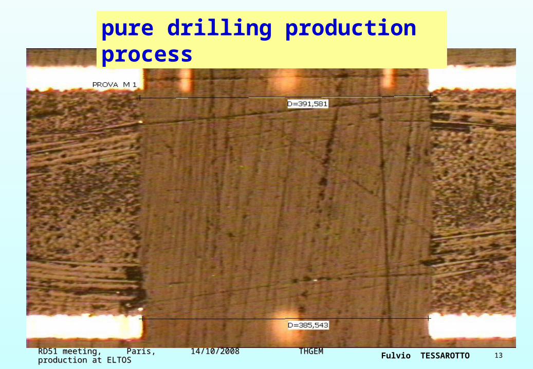
pure drilling production process

Fulvio TESSAROTTO RD51 meeting, Paris, 14/10/2008 THGEM production at ELTOSRD51 meeting, Paris, 14/10/2008 THGEM production at ELTOS 1414
double drilling production process

Fulvio TESSAROTTO RD51 meeting, Paris, 14/10/2008 THGEM production at ELTOSRD51 meeting, Paris, 14/10/2008 THGEM production at ELTOS 1515
Vmax (= discharge limit in pure N2)For the characterization of the small prototypes, listen to Elena Rocco and Jaroslav Polak talks tomorrow
different production techniques different behaviors

Fulvio TESSAROTTO RD51 meeting, Paris, 14/10/2008 THGEM production at ELTOSRD51 meeting, Paris, 14/10/2008 THGEM production at ELTOS 1616
The second series of small size The second series of small size piecespieces
NAME RIM (mm) THICKNESS (mm) Ø (mm) PITCH (mm)
M2.1 0.4 0.3 0.8
M2.2 0.4 0.2 0.8
M2.3 0.4 0.3 1.2
M2.4 0.6 0.4 0.8
M2.5 0.6 0.3 0.8
M2.6 0.6 0.4 1
M2.7 0.6 0.3 1
M2.10 0.8 0.4 0.8
M2.11 0.8 0.3 0.8
M2.12 0.8 0.4 1
M2.13 0.8 0.3 1
C2.1 0.002 0.6 0.3 1
C2.2 0.005 0.6 0.3 1
C2.3 0.010 0.6 0.3 1

Fulvio TESSAROTTO RD51 meeting, Paris, 14/10/2008 THGEM production at ELTOSRD51 meeting, Paris, 14/10/2008 THGEM production at ELTOS 1717
th. 0.8, diam. 0.4, no rimth. 0.8, diam. 0.4, no rim
Fulvio TESSAROTTO RD51 meeting, Paris, 14/10/2008 THGEM production at ELTOSRD51 meeting, Paris, 14/10/2008 THGEM production at ELTOS 1818
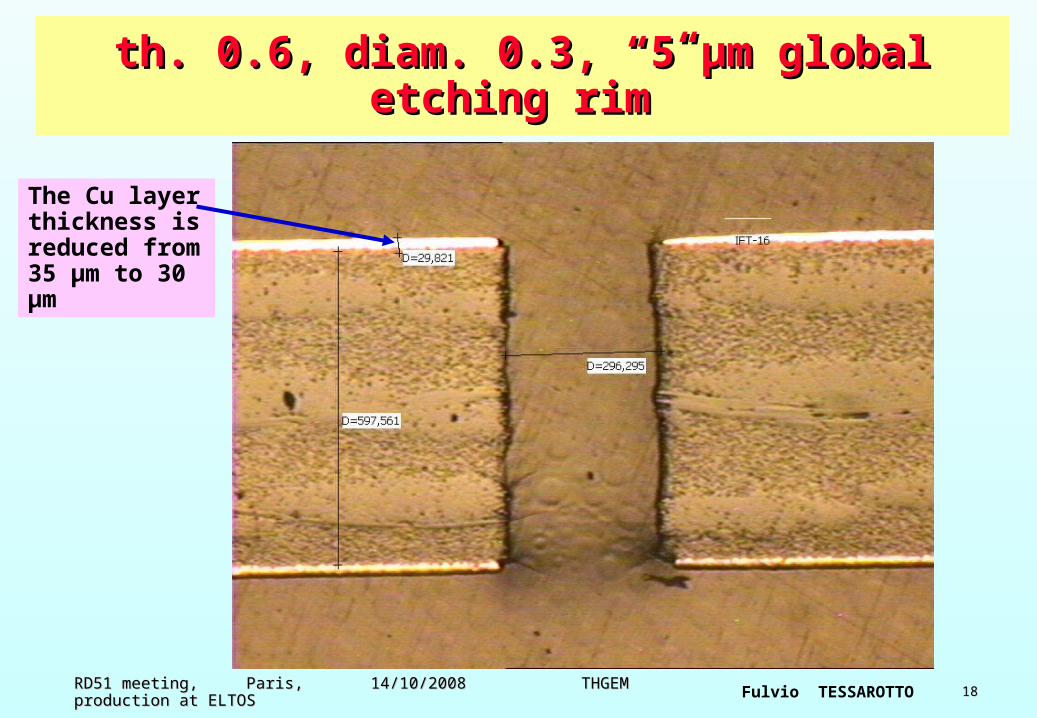
th. 0.6, diam. 0.3, “5 th. 0.6, diam. 0.3, “5 μμm global etching m global etching rim”rim”
The Cu layer thickness is reduced from 35 μm to 30 μm

Fulvio TESSAROTTO RD51 meeting, Paris, 14/10/2008 THGEM production at ELTOSRD51 meeting, Paris, 14/10/2008 THGEM production at ELTOS 1919
The prototypes from this second set are presently being characterized, and a third set will probably be ordered.
Several tests have been performed with prototype detectors having double and triple THGEM layers.
UV photon detection by CsI coated THGEMS is also currently being studied.
These items will be covered in the talks by E. Rocco and J. Polak.
All pieces were providing readable signals.
None has ever beeen damaged, despite large discharges.
We wish to investigate the problems related to large area detector construction, in particular the production of larger area THGEMs

Fulvio TESSAROTTO RD51 meeting, Paris, 14/10/2008 THGEM production at ELTOSRD51 meeting, Paris, 14/10/2008 THGEM production at ELTOS 2020
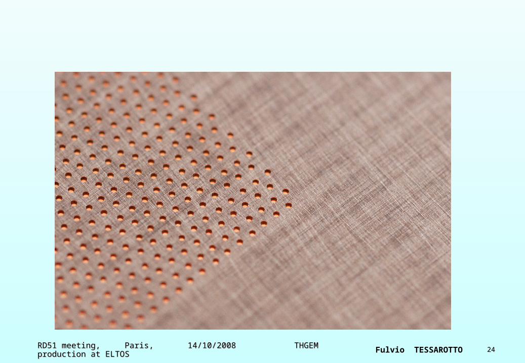
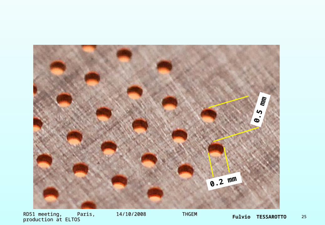
CERN produced 100 x 100 mm2 THGEM
thickness: 0.2 mm diameter: 0.2 mm pitch: 0.5 mm rim: ~ 10 μm
Fulvio TESSAROTTO RD51 meeting, Paris, 14/10/2008 THGEM production at ELTOSRD51 meeting, Paris, 14/10/2008 THGEM production at ELTOS 2121
Fulvio TESSAROTTO RD51 meeting, Paris, 14/10/2008 THGEM production at ELTOSRD51 meeting, Paris, 14/10/2008 THGEM production at ELTOS 2222
Fulvio TESSAROTTO RD51 meeting, Paris, 14/10/2008 THGEM production at ELTOSRD51 meeting, Paris, 14/10/2008 THGEM production at ELTOS 2323
Fulvio TESSAROTTO RD51 meeting, Paris, 14/10/2008 THGEM production at ELTOSRD51 meeting, Paris, 14/10/2008 THGEM production at ELTOS 2424
Fulvio TESSAROTTO RD51 meeting, Paris, 14/10/2008 THGEM production at ELTOSRD51 meeting, Paris, 14/10/2008 THGEM production at ELTOS 2525
0.2 mm
0.5 mm
Fulvio TESSAROTTO RD51 meeting, Paris, 14/10/2008 THGEM production at ELTOSRD51 meeting, Paris, 14/10/2008 THGEM production at ELTOS 2626
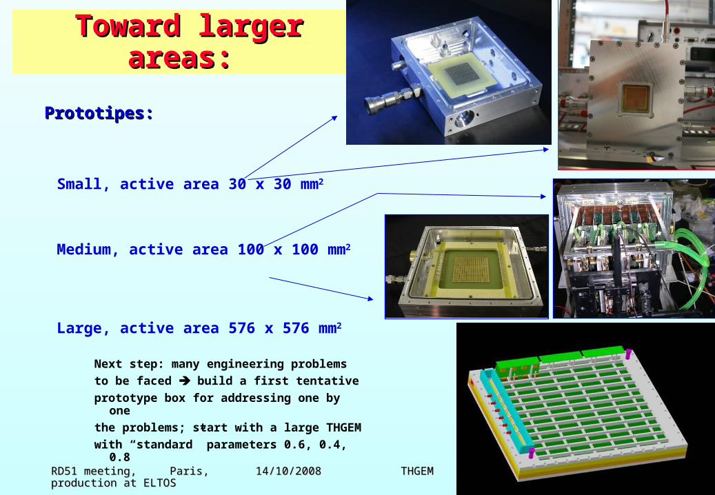
Toward larger Toward larger areas:areas:
Prototipes:Prototipes:
Small, active area 30 x 30 mm2
Medium, active area 100 x 100 mm2
Large, active area 576 x 576 mm2
Next step: many engineering problems
to be faced build a first tentative
prototype box for addressing one by one
the problems; start with a large THGEM
with “standard” parameters 0.6, 0.4, 0.8

Fulvio TESSAROTTO RD51 meeting, Paris, 14/10/2008 THGEM production at ELTOSRD51 meeting, Paris, 14/10/2008 THGEM production at ELTOS 2727
600 mm
600 mm
THGEMsStesalite frames
Al frame
Anode pads
Structure of Structure of the large the large
areaareaprototype prototype detectordetector
Al frame
Fulvio TESSAROTTO RD51 meeting, Paris, 14/10/2008 THGEM production at ELTOSRD51 meeting, Paris, 14/10/2008 THGEM production at ELTOS 2828
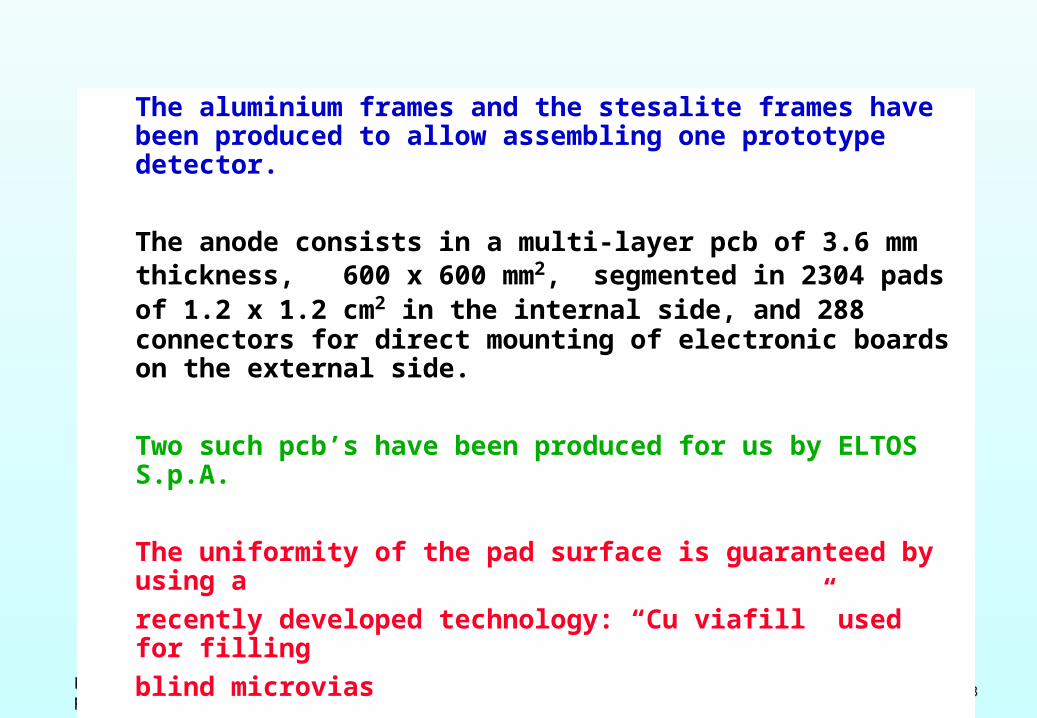
The aluminium frames and the stesalite frames have been produced to allow assembling one prototype detector.
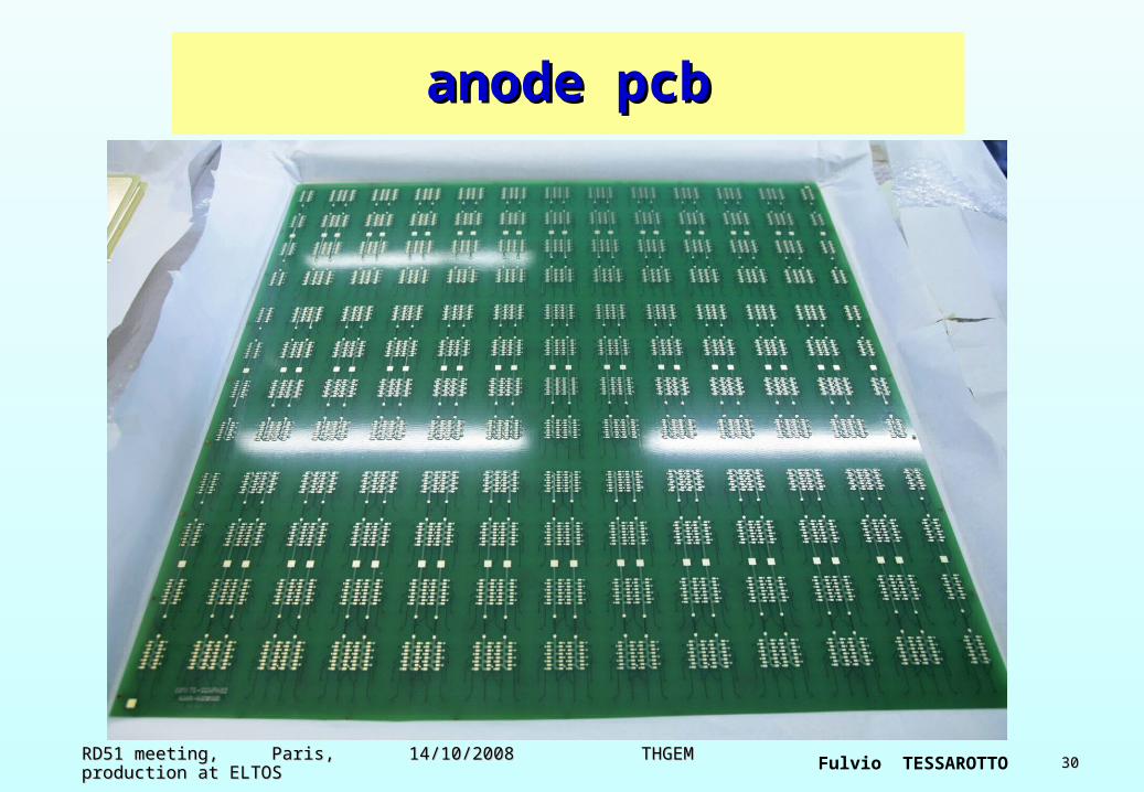
The anode consists in a multi-layer pcb of 3.6 mm thickness, 600 x 600 mm2, segmented in 2304 pads of 1.2 x 1.2 cm2 in the internal side, and 288 connectors for direct mounting of electronic boards on the external side.
Two such pcb’s have been produced for us by ELTOS S.p.A.
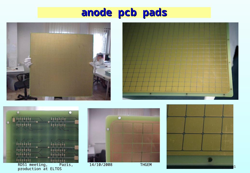
The uniformity of the pad surface is guaranteed by using a
recently developed technology: “Cu viafill” used for filling
blind microvias

Fulvio TESSAROTTO RD51 meeting, Paris, 14/10/2008 THGEM production at ELTOSRD51 meeting, Paris, 14/10/2008 THGEM production at ELTOS 2929
Cu viafill technology
Fulvio TESSAROTTO RD51 meeting, Paris, 14/10/2008 THGEM production at ELTOSRD51 meeting, Paris, 14/10/2008 THGEM production at ELTOS 3030
anode pcbanode pcb
Fulvio TESSAROTTO RD51 meeting, Paris, 14/10/2008 THGEM production at ELTOSRD51 meeting, Paris, 14/10/2008 THGEM production at ELTOS 3131
anode pcb padsanode pcb pads
Fulvio TESSAROTTO RD51 meeting, Paris, 14/10/2008 THGEM production at ELTOSRD51 meeting, Paris, 14/10/2008 THGEM production at ELTOS 3232
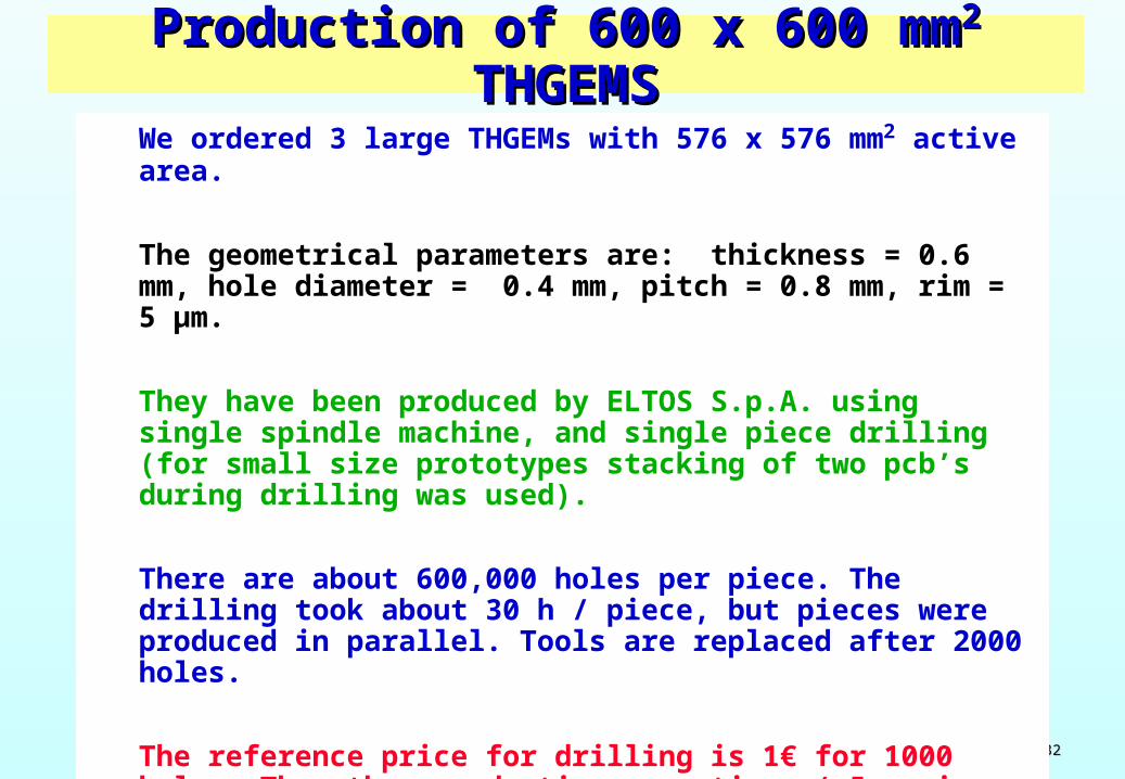
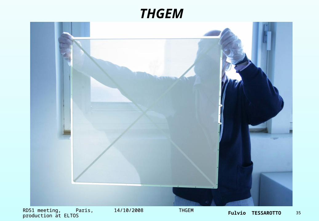
We ordered 3 large THGEMs with 576 x 576 mm2 active area.
The geometrical parameters are: thickness = 0.6 mm, hole diameter = 0.4 mm, pitch = 0.8 mm, rim = 5 μm.
They have been produced by ELTOS S.p.A. using single spindle machine, and single piece drilling (for small size prototypes stacking of two pcb’s during drilling was used).
There are about 600,000 holes per piece. The drilling took about 30 h / piece, but pieces were produced in parallel. Tools are replaced after 2000 holes.
The reference price for drilling is 1€ for 1000 holes. The other production operations (~5μm rim, Ni-Au, …) add a similar amount to the final price.
Production of 600 x 600 mmProduction of 600 x 600 mm22 THGEMSTHGEMS
Fulvio TESSAROTTO RD51 meeting, Paris, 14/10/2008 THGEM production at ELTOSRD51 meeting, Paris, 14/10/2008 THGEM production at ELTOS 3333
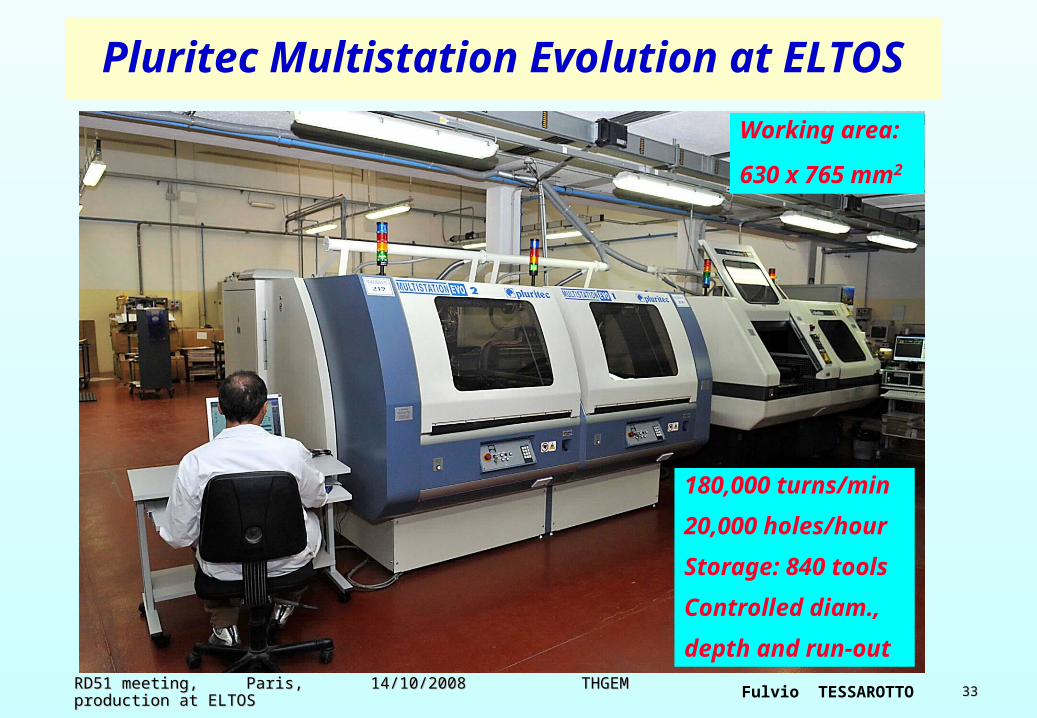
Pluritec Multistation Evolution at ELTOS
180,000 turns/min
20,000 holes/hour
Storage: 840 tools
Controlled diam.,
depth and run-out
Working area:
630 x 765 mm2
Fulvio TESSAROTTO RD51 meeting, Paris, 14/10/2008 THGEM production at ELTOSRD51 meeting, Paris, 14/10/2008 THGEM production at ELTOS 3434
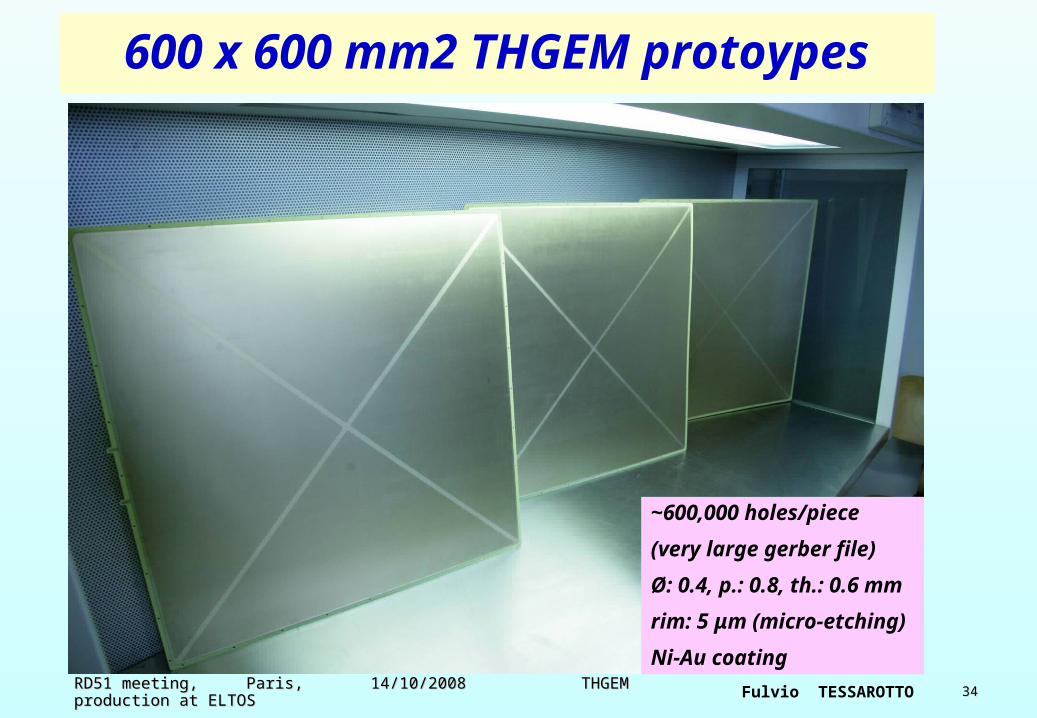
600 x 600 mm2 THGEM protoypes
~600,000 holes/piece
(very large gerber file)
Ø: 0.4, p.: 0.8, th.: 0.6 mm
rim: 5 μm (micro-etching)
Ni-Au coating
Fulvio TESSAROTTO RD51 meeting, Paris, 14/10/2008 THGEM production at ELTOSRD51 meeting, Paris, 14/10/2008 THGEM production at ELTOS 3535
THGEM

Fulvio TESSAROTTO RD51 meeting, Paris, 14/10/2008 THGEM production at ELTOSRD51 meeting, Paris, 14/10/2008 THGEM production at ELTOS 3636
600 x 600 mm2
THGEMs

Fulvio TESSAROTTO RD51 meeting, Paris, 14/10/2008 THGEM production at ELTOSRD51 meeting, Paris, 14/10/2008 THGEM production at ELTOS 3737
ConclusionsConclusionsThe ELTOS S.p.A. Company in Italy has recently gained significant experience in the production of THGEM prototypes of many different types.
In order to optimize the procedures for THGEM production it is very important to know the production details and to correlate them to the performances of the prototypes.
This work has started with a large set of 30 x 30 mm2 THGEMS which have been delivered and tested.
The first set of 600 x 600 mm2 THGEMs has been produced and delivered last week.
Industrial production of THGEMs may be close to become real.


![Thick GEM versus thin GEM in two-phase argon avalanche ... · presented elsewhere [15,16,18,28]. Here we describe details relevant to THGEM performance in general and to THGEM and](https://img.pdfslide.net/doc/110x75/601aa2bd1fb51279164b0325/thick-gem-versus-thin-gem-in-two-phase-argon-avalanche-presented-elsewhere-15161828.jpg)