Embed Size (px)
Citation preview

International Journal of Scientific & Engineering Research, Volume 6, Issue 7, July-2015 1664 ISSN 2229-5518
IJSER © 2015 http://www.ijser.org
Etching Effect on Sensing Behavior of CuO:NiO/PS Hydrogen Gas Sensor
Isam M. Ibrahim1, Yahya R. Hathal1,2, Fuad T. Ibrahim1 and Mudhafar H. ALI*2
Abstract— In this paper, thin films of copper oxide nanoparticles mixed with 2% wt of nickel oxide are deposited on glass and porous silicon (PS) substrates with orientation (111) etched at 30 minutes. The current density was varied from (10 to 50) mA/cm2 with a step of 10 utilizing pulsed laser deposition technique for the manufacture of hydrogen gas sensor. The films are annealed in air at 400 °C for two hours. The PL result of PS shows that the peak position is shifted to the higher wavelength region due to increase etching current. On the other hand, the atomic force microscopy shows an increase in average diameter with increasing etching current (10-30) mA then decrease. Moreover, the FTIR spectra of porous silicon exhibit that the pore surface includes a high density of dangling bonds of Si for original impurities such as hydrogen and fluorine, which are residuals from the electrolyte. Finally the sensitivity of the hydrogen gas sensor are increased with increasing operating temperature.
Index Terms— Gas Sensors, Pulsed Laser Deposition, Metal Oxide, Atomic Force Microscope
—————————— ——————————
1 INTRODUCTION Hydrogen gas is tasteless, colorless and odorless so it
cannot be detected by human beings. The low ignition energy and wide flammable range makes it easy inflammable and explosive. Therefore rapid and accurate hydrogen detection is necessary during the production, storage and use of hydrogen and it is also essential for monitoring/controlling the hydrogen concentration of nuclear reactors, coal mines and semiconductor manufacturing [1].
Porous silicon (PS) a nanostructured material, has attracted considerable attention as a measure to enhance the optical properties of silicon (Si). The formation of PS layers on crystalline Si (c-Si) wafers using electrochemical etching (ECE) exhibits photo luminescent and electroluminescent properties similar to those of semiconductors with direct energy gap . PS has emerged as an attractive material in the field of electronics and optoelectronics due to its broad band gap, wide optical transmission range (700–1000 nm), wide absorption spectrum, surface roughening and good anti-reflection coating (ARC). The surface roughness and lower effective refractive index, which can reduce the reflection losses of sunlight radiation are the primary factors that enhance PS compared with c-Si[2].
The physical properties of porous silicon are fundamentally determined by the shape, diameter of pores, porosity, and the thickness of the formed porous layer.
———————————————— 1 Department of physics, College of Science, University of Baghdad,
Baghdad, Iraq. 2 Rewnable Energy Center, Ministry of Science and Technology,
Baghdad, Iraq. * Corresponding Author: [email protected]
Depending on the etching parameters, for example current density, HF concentration, or substrate doping type and
level, the physical properties of PS can be varied. In addition, when the feature size of the pores of PS is less than a few nanometers, various quantum-size effects occur, which make PS even more fascinating [3].
Oxide semiconductors been used to detect oxidizing
and reducing gases in simple and cost-effective have manner[4]. Their chemiresistive variation emanates from the oxidative or reductive interaction of the analytic gas with the oxide semiconductor surface and the consequent change in the charge carrier concentration. In p-type oxide semiconductor gas sensors such as those comprising CuO, NiO, Co3O4, and Cr2O3, the adsorption of negatively charged oxygen forms a hole accumulation layer near the surface. Thus, conduction occurs along the conductive hole accumulation layer[5].
Copper oxides are semiconductors and have been studied for several reasons such as: the natural abundance of starting material (Cu), the easiness of production by Cu oxidation, their non-toxic nature and the reasonably good electrical and optical properties exhibited by Cu2O. Cupric oxide (CuO) is a p-type semiconductor having a band gap of 1.21–1.51 eV and monoclinic crystal structure [6]. Copper oxides are used for gas sensors for hydrogen, volatile organic compounds catalysis and specially cuprous oxide films were intensively researched in device applications such as photovoltaic solar cell, photo electrochemical cell and electrochromic coatings [7]
Nickel oxide (NiO) is p-type semiconductor material and is widely used in different applications such as transparent conductive films and electrochromic devices, as a potential candidate in the chemical sensors. NiO exhibits a wide band gap of 3.6–4.0 eV at room temperature; thus, NiO is considered transparent in the visible light region. Moreover, NiO is largely used as a catalyst with different n-type semiconductors due its high p-type concentration, high hole mobility and low cost. The existence of NiO enhances the separation of electron and hole pairs via
IJSER
International Journal of Scientific & Engineering Research, Volume 6, Issue 7, July-2015 1665 ISSN 2229-5518
IJSER © 2015 http://www.ijser.org
electric junction field and also promotes the interfacial charge transfer[8].
Also, it was found that the addition of NiO to CuO brought a significant increase in the degree of crystallinity of the mixed oxides which is accompanying with an increase in their particle size and a decrease in the surface area. Moreover, addition of NiO to CuO, also reduces the amount of surface excess oxygen of CuO due to a synergistic effect [9].
2 EXPERIMENTAL SETUP Copper oxide nanoparticles with 2% wt. of nickel
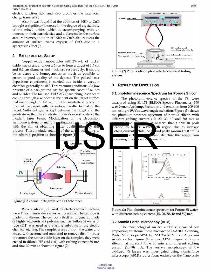
oxide was pressed under a 5 ton to form a target of 1.5 cm and 0.2 cm diameter and thickness respectively. It should be as dense and homogeneous as much as possible to ensure a good quality of the deposit. The pulsed laser deposition experiment is carried out inside a vacuum chamber generally at 10-3 Torr vacuum conditions. At low pressure of a background gas for specific cases of oxides and nitrides. The focused Nd:YAG Q-switching laser beam coming through a window is incident on the target surface making an angle of 45° with it. The substrate is placed in front of the target with its surface parallel to that of the target. Sufficient gap is kept between the target and the substrate so that the substrate holder does not obstruct the incident laser beam. Modification of the deposition technique is done by many investigators from time to time with the aim of obtaining better quality films by this process. These include rotation of the target according to the substrate position as shown in figure (1).
Figure (1) Schematic diagram of a PLD chamber.
Porous silicon prepared by electrochemical etching
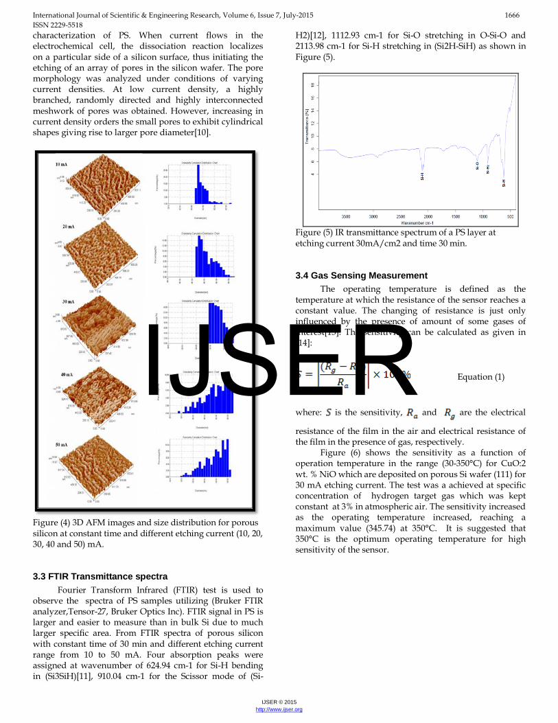
were The silicon wafer serves as the anode. The cathode is made of platinum. The cell body itself is, in general, made of highly acid-resistant polymer such as Teflon .Si wafer p-type (111) was used as a starting substrate in the electro chemical etching. The samples were cut from the wafer and rinsed with acetone and methanol to remove dirt. In order to remove the native oxide layer on the samples, they were etched in diluted HF acid (1:1) with etching current 30 mA and time 30 min as shown in figure (2).
Figure (2) Porous silicon photo-electrochemical testing system.
3 2BRESULT AND DISCUSSION
5B3.1 photoluminescence Spectrum for Porous Silicon The photoluminescence spectra of the PS, were
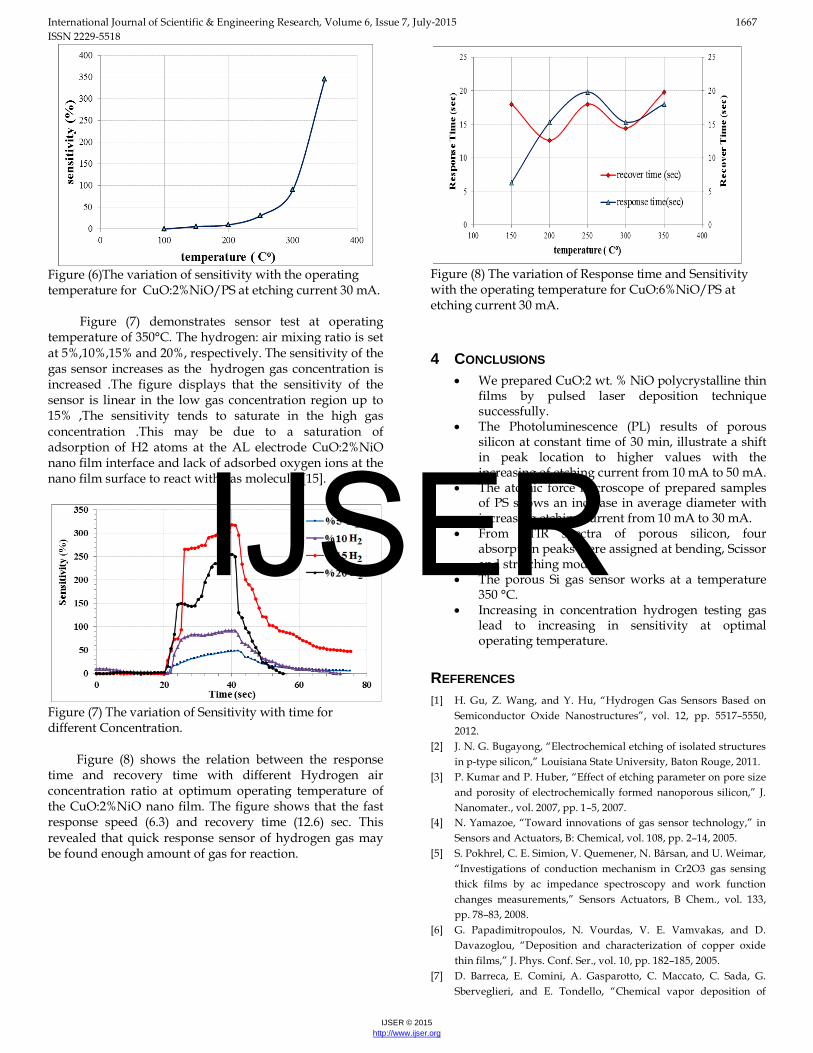
measured using SL-174 (ELICO) Spectro Fluormeter, 150 watt Xenon Arc lamp, Excitation and emission from 200-900 nm using 4.49eVas wavelength excitation. Figure (3) shows the photoluminescence spectrum of porous silicon with different etching current (10, 20, 30, 40 and 50) mA at constant time (30 min). Its observe that a shift in peak location to higher wavelength region due to increase etching current. While the second peaks (around 600 nm) is due to the surface state of nano structure that arises from increasing of surface to volume ratio.
Figure (3) Photoluminescence spectrum for Porous Si wafer with different etching current (10, 20, 30, 40 and 50) mA.
6B3.2 Atomic Force Microscopy (AFM) The morphological surface analysis is carried out
employing an atomic force microscope (AA3000 Scanning Probe Microscope SPM, tip NSC35/AIBS from Angstrom Ad-Vance Inc Figure (4) shows AFM images of porous silicon at constant time 30 min and different etching current (10-50) mA. The surface morphology of the oxidized PS layers was investigated using atomic force microscope (AFM) studies focus entirely on the Nano scale
IJSER
International Journal of Scientific & Engineering Research, Volume 6, Issue 7, July-2015 1666 ISSN 2229-5518
IJSER © 2015 http://www.ijser.org
characterization of PS. When current flows in the electrochemical cell, the dissociation reaction localizes on a particular side of a silicon surface, thus initiating the etching of an array of pores in the silicon wafer. The pore morphology was analyzed under conditions of varying current densities. At low current density, a highly branched, randomly directed and highly interconnected meshwork of pores was obtained. However, increasing in current density orders the small pores to exhibit cylindrical shapes giving rise to larger pore diameter[10].
Figure (4) 3D AFM images and size distribution for porous silicon at constant time and different etching current (10, 20, 30, 40 and 50) mA.
3.3 FTIR Transmittance spectra Fourier Transform Infrared (FTIR) test is used to
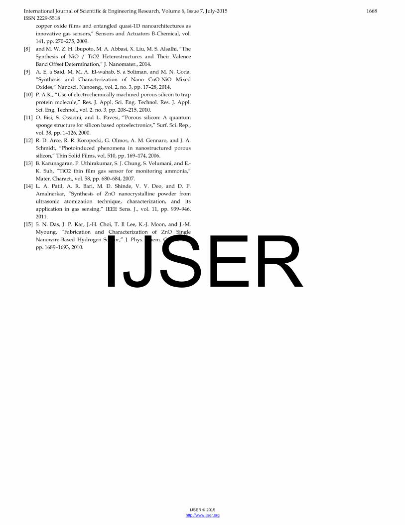
observe the spectra of PS samples utilizing (Bruker FTIR analyzer,Tensor-27, Bruker Optics Inc). FTIR signal in PS is larger and easier to measure than in bulk Si due to much larger specific area. From FTIR spectra of porous silicon with constant time of 30 min and different etching current range from 10 to 50 mA. Four absorption peaks were assigned at wavenumber of 624.94 cm-1 for Si-H bending in (Si3SiH)[11], 910.04 cm-1 for the Scissor mode of (Si-
H2)[12], 1112.93 cm-1 for Si-O stretching in O-Si-O and 2113.98 cm-1 for Si-H stretching in (Si2H-SiH) as shown in Figure (5).
Figure (5) IR transmittance spectrum of a PS layer at etching current 30mA/cm2 and time 30 min.
8B3.4 Gas Sensing Measurement The operating temperature is defined as the
temperature at which the resistance of the sensor reaches a constant value. The changing of resistance is just only influenced by the presence of amount of some gases of interest[13]. The sensitivity can be calculated as given in [14]:
Equation (1)
where: is the sensitivity, and are the electrical
resistance of the film in the air and electrical resistance of the film in the presence of gas, respectively.
Figure (6) shows the sensitivity as a function of operation temperature in the range (30-350°C) for CuO:2 wt. % NiO which are deposited on porous Si wafer (111) for 30 mA etching current. The test was a achieved at specific concentration of hydrogen target gas which was kept constant at 3% in atmospheric air. The sensitivity increased as the operating temperature increased, reaching a maximum value (345.74) at 350°C. It is suggested that 350°C is the optimum operating temperature for high sensitivity of the sensor.
IJSER
International Journal of Scientific & Engineering Research, Volume 6, Issue 7, July-2015 1667 ISSN 2229-5518
IJSER © 2015 http://www.ijser.org
Figure (6)The variation of sensitivity with the operating temperature for CuO:2%NiO/PS at etching current 30 mA. Figure (7) demonstrates sensor test at operating temperature of 350°C. The hydrogen: air mixing ratio is set at 5%,10%,15% and 20%, respectively. The sensitivity of the gas sensor increases as the hydrogen gas concentration is increased .The figure displays that the sensitivity of the sensor is linear in the low gas concentration region up to 15% ,The sensitivity tends to saturate in the high gas concentration .This may be due to a saturation of adsorption of H2 atoms at the AL electrode CuO:2%NiO nano film interface and lack of adsorbed oxygen ions at the nano film surface to react with gas molecules[15].
Figure (7) The variation of Sensitivity with time for different Concentration.
Figure (8) shows the relation between the response time and recovery time with different Hydrogen air concentration ratio at optimum operating temperature of the CuO:2%NiO nano film. The figure shows that the fast response speed (6.3) and recovery time (12.6) sec. This revealed that quick response sensor of hydrogen gas may be found enough amount of gas for reaction.
Figure (8) The variation of Response time and Sensitivity with the operating temperature for CuO:6%NiO/PS at etching current 30 mA.
4 CONCLUSIONS • We prepared CuO:2 wt. % NiO polycrystalline thin
films by pulsed laser deposition technique successfully.
• The Photoluminescence (PL) results of porous silicon at constant time of 30 min, illustrate a shift in peak location to higher values with the increasing of etching current from 10 mA to 50 mA.
• The atomic force microscope of prepared samples of PS shows an increase in average diameter with increasing etching current from 10 mA to 30 mA.
• From FTIR spectra of porous silicon, four absorption peaks were assigned at bending, Scissor and stretching mode.
• The porous Si gas sensor works at a temperature 350 °C.
• Increasing in concentration hydrogen testing gas lead to increasing in sensitivity at optimal operating temperature.
REFERENCES [1] H. Gu, Z. Wang, and Y. Hu, “Hydrogen Gas Sensors Based on
Semiconductor Oxide Nanostructures”, vol. 12, pp. 5517–5550, 2012.
[2] J. N. G. Bugayong, “Electrochemical etching of isolated structures in p-type silicon,” Louisiana State University, Baton Rouge, 2011.
[3] P. Kumar and P. Huber, “Effect of etching parameter on pore size and porosity of electrochemically formed nanoporous silicon,” J. Nanomater., vol. 2007, pp. 1–5, 2007.
[4] N. Yamazoe, “Toward innovations of gas sensor technology,” in Sensors and Actuators, B: Chemical, vol. 108, pp. 2–14, 2005.
[5] S. Pokhrel, C. E. Simion, V. Quemener, N. Bârsan, and U. Weimar, “Investigations of conduction mechanism in Cr2O3 gas sensing thick films by ac impedance spectroscopy and work function changes measurements,” Sensors Actuators, B Chem., vol. 133, pp. 78–83, 2008.
[6] G. Papadimitropoulos, N. Vourdas, V. E. Vamvakas, and D. Davazoglou, “Deposition and characterization of copper oxide thin films,” J. Phys. Conf. Ser., vol. 10, pp. 182–185, 2005.
[7] D. Barreca, E. Comini, A. Gasparotto, C. Maccato, C. Sada, G. Sberveglieri, and E. Tondello, “Chemical vapor deposition of
IJSER
International Journal of Scientific & Engineering Research, Volume 6, Issue 7, July-2015 1668 ISSN 2229-5518
IJSER © 2015 http://www.ijser.org
copper oxide films and entangled quasi-1D nanoarchitectures as innovative gas sensors,” Sensors and Actuators B-Chemical, vol. 141, pp. 270–275, 2009.
[8] and M. W. Z. H. Ibupoto, M. A. Abbasi, X. Liu, M. S. Alsalhi, “The Synthesis of NiO / TiO2 Heterostructures and Their Valence Band Offset Determination,” J. Nanomater., 2014.
[9] A. E. a Said, M. M. A. El-wahab, S. a Soliman, and M. N. Goda, “Synthesis and Characterization of Nano CuO-NiO Mixed Oxides,” Nanosci. Nanoeng., vol. 2, no. 3, pp. 17–28, 2014.
[10] P. A.K., “Use of electrochemically machined porous silicon to trap protein molecule,” Res. J. Appl. Sci. Eng. Technol. Res. J. Appl. Sci. Eng. Technol., vol. 2, no. 3, pp. 208–215, 2010.
[11] O. Bisi, S. Ossicini, and L. Pavesi, “Porous silicon: A quantum sponge structure for silicon based optoelectronics,” Surf. Sci. Rep., vol. 38, pp. 1–126, 2000.
[12] R. D. Arce, R. R. Koropecki, G. Olmos, A. M. Gennaro, and J. A. Schmidt, “Photoinduced phenomena in nanostructured porous silicon,” Thin Solid Films, vol. 510, pp. 169–174, 2006.
[13] B. Karunagaran, P. Uthirakumar, S. J. Chung, S. Velumani, and E.-K. Suh, “TiO2 thin film gas sensor for monitoring ammonia,” Mater. Charact., vol. 58, pp. 680–684, 2007.
[14] L. A. Patil, A. R. Bari, M. D. Shinde, V. V. Deo, and D. P. Amalnerkar, “Synthesis of ZnO nanocrystalline powder from ultrasonic atomization technique, characterization, and its application in gas sensing,” IEEE Sens. J., vol. 11, pp. 939–946, 2011.
[15] S. N. Das, J. P. Kar, J.-H. Choi, T. Il Lee, K.-J. Moon, and J.-M. Myoung, “Fabrication and Characterization of ZnO Single Nanowire-Based Hydrogen Sensor,” J. Phys. Chem. C, vol. 114, pp. 1689–1693, 2010.
IJSER