Embed Size (px)
Citation preview

1Introduction
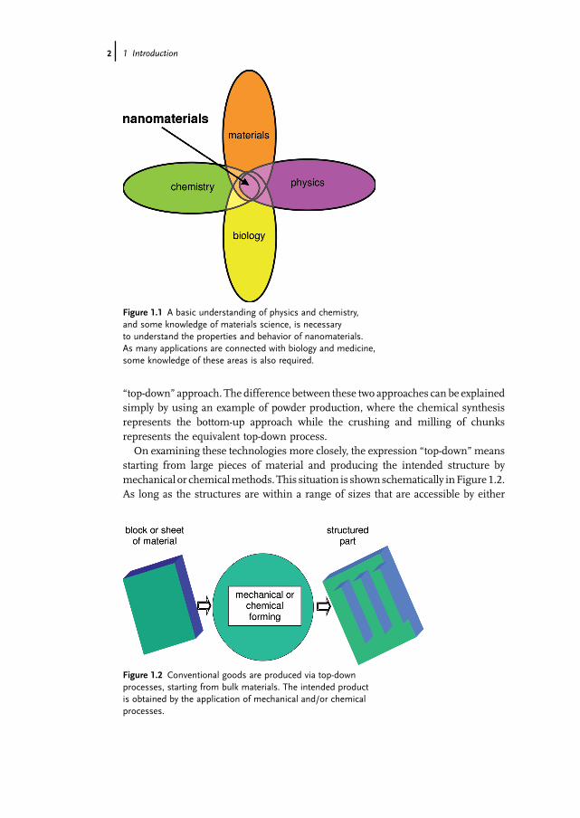
Today, everybody is talking about nanomaterials and, indeed, verymany publications,books, and journals are devoted to this topic. Usually, such publications are directedtowards specialists such as physicists and chemists, and the �classic� materialsscientist encounters increasing problems in understanding the situation. Moreover,those people who are interested in the subject but who have no specific education inany of these fields have virtually no chance of understanding the development of thistechnology. It is the aim of this book to fill this gap. The book will focus on the specialphenomena related to nanomaterials and attempt to provide explanations whichavoid – as far as possible – any highly theoretical and quantum mechanical descrip-tions. The difficulties with nanomaterials arise from the fact that, in contrast toconventional materials, a profound knowledge of materials science is not sufficient.The cartoon shown in Figure 1.1 shows that nanomaterials lie at the intersectionof materials science, physics, chemistry, and – for many of the most interestingapplications – also of biology and medicine.However, this situation is less complicated than it first appears to the observer, as
the number of additional facts introduced to materials science is not that large.Nonetheless, the user of nanomaterials must accept that the properties of the lattermaterials demand a deeper insight into their physics and chemistry. Whereas, forconventionalmaterials the interface to biotechnology andmedicine is related directlyto the application, the situation is different in nanotechnology, where biologicalmolecules such as proteins or DNA are also used as building blocks for applicationsoutside biology and medicine.So, the first question to be asked is, �What are nanomaterials?� There are two
definitions. The first – and broadest – definition states that nanomaterials arematerials where the sizes of the individual building blocks are less than 100 nm,at least in one dimension. This definition is well suited for many research proposals,where nanomaterials have a high priority. The second definition is much morerestrictive, and states that nanomaterials have propertieswhich depend inherently onthe small grain size and, as nanomaterials are usually quite expensive, such arestrictive definition makes more sense. The main difference between nanotechnol-ogy and conventional technologies is that the �bottom-up� approach (see below) ispreferred in nanotechnology, whereas conventional technologies usually use the
Nanomaterials: An Introduction to Synthesis, Properties and Application. Dieter VollathCopyright � 2008 WILEY-VCH Verlag GmbH & Co. KGaA, WeinheimISBN: 978-3-527-31531-4
j1
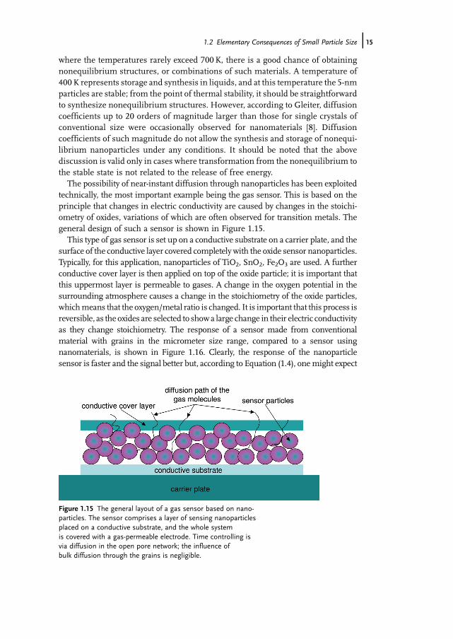
�top-down� approach. The difference between these two approaches can be explainedsimply by using an example of powder production, where the chemical synthesisrepresents the bottom-up approach while the crushing and milling of chunksrepresents the equivalent top-down process.On examining these technologies more closely, the expression �top-down� means
starting from large pieces of material and producing the intended structure bymechanical or chemicalmethods. This situation is shownschematically inFigure 1.2.As long as the structures are within a range of sizes that are accessible by either
Figure 1.1 A basic understanding of physics and chemistry,and some knowledge of materials science, is necessaryto understand the properties and behavior of nanomaterials.As many applications are connected with biology and medicine,some knowledge of these areas is also required.
Figure 1.2 Conventional goods are produced via top-downprocesses, starting from bulk materials. The intended productis obtained by the application of mechanical and/or chemicalprocesses.
2j 1 Introduction

mechanical tools or photolithographic processes, then top-down processes have anunmatched flexibility in their application.The situation is different in �bottom-up� processes, in which atoms or molecules
are used as the building blocks to produce nanoparticles, nanotubes or nanorods, orthin films or layered structures. According to their dimensionality, these features arealso referred to as zero-, one-, or two-dimensional nanostructures (see Figure 1.3).Figure 1.3 also demonstrates the building of particles, layers, nanotubes, or nanorodsfrom atoms (ions) or molecules. Although such processes provide tremendousfreedom among the resultant products, the number of possible structures to beobtained is comparatively small. In order to obtain ordered structures, bottom-upprocesses (as described above) must be supplemented by the self-organization ofindividual particles.Often, top-down technologies are described as being �subtractive�, in contrast to
the �additive� technologies which describe bottom-up processes. The crucial prob-lem is no longer to produce these elements of nanotechnology; rather, it is theirincorporation into technical parts. The size ranges of classical top-down technologiescompared to bottom-up technologies are shown graphically in Figure 1.4. Clearly,there is a broad range of overlappingwhere improved top-down technologies, such aselectron beam or X-ray lithography, enter the size range typical of nanotechnologies.Currently, these improved top-down technologies are penetrating into increasingnumbers of fields of application.For industrial applications, the most important question is the product�s price in
relation to its properties. In most cases, nanomaterials and products utilizingnanomaterials are significantly more expensive than conventional products. In thecase of nanomaterials, the increase in price is sometimesmore pronounced than theimprovement in properties, and therefore economically interesting applications ofnanomaterials are often found only in areas where specific properties are demandedthat are beyond the reach of conventional materials. Hence, as long as the use ofnanomaterials with new properties provides the solution to a problem which cannot
Figure 1.3 Nanotechnologies are usually connected to bottom-upprocesses, and are characterized by the use of atoms ormoleculesas building blocks. Bottom-up processes result in particles,nanotubes, nanorods, thin films, or layered structures.
1 Introduction j3

be solved with conventional materials, the price becomes much less important.Another point is that, as the applications of nanomaterials using improved propertiesare in direct competition to well-established conventional technologies, they willencounter afierce price competition, and thismay lead tomajor problems for a youngand expensive technology to overcome. Indeed, it is often observed that marginalprofit margins in the production or application of nanomaterials with improvedpropertiesmay result in severe financial difficulties for newly founded companies. Ingeneral, the economically successful application of nanomaterials requires only asmall amount of material as compared to conventional technologies; hence, one isselling �knowledge� rather than �tons� (see Table 1.1). Finally, only those materialswhich exhibit new properties leading to novel applications, beyond the reach ofconventional materials, promise interesting economic results.
Figure 1.4 The estimated lateral limits of different structuringprocesses. Clearly, the size range of bottom-up and conventionaltop-down processes is limited. New, advanced top-down pro-cesses expand the size range of their conventional counterparts,and enter the size range typical of bottom-up processes.
Table 1.1 The relationship between the properties of a newproduct and prices, quantities, and expected profit.
Properties Price Quantity Profits
Low High Small Large
Improved X – – X Questionable
New – X X – Potentially high
Note: only those products with new properties promise potentially high profits.
4j 1 Introduction

1.1Nanomaterials and Nanocomposites
Nanomaterialsmay be zero-dimensional (e.g., nanoparticles), one-dimensional (e.g.,nanorods or nanotubes), or two-dimensional (usually realized as thin films or stacksof thin films). As a typical example, an electron micrograph of zirconia powder (azero-dimensional object) is shown in Figure 1.5.The particles depicted in Figure 1.5 show a size of ca. 7 nm, and also a very narrow
range of sizes. This is an important point, asmany of the properties of nanomaterialsare size-dependent. In contrast, many applications do not require such sophistica-tion, and therefore cheaper materials with a broader particle size distribution (seeFigure 1.6a) would be sufficient. Thematerial depicted in Figure 1.6a, which containsparticles ranging in size from 5 to more than 50 nm, would be perfectly suited forapplications such as pigments or ultra-violet (UV) absorbers.A further interesting class of particles may be described as fractal clusters of
extreme small particles. Typical examples of this type of material are most of theamorphous silica particles (known as �white soot�) and amorphous Fe2O3 particles,the latter being used as catalysts (see Figure 1.6b).Apart from properties related to grain boundaries, the special properties of
nanomaterials are those of single isolated particles that are altered, or even lost, inthe case of particle interaction. Therefore,most of the basic considerations are relatedto isolated nanoparticles as the interaction of two or more particles may causesignificant changes in the properties. For technical applications, this proved to benegative, and consequently nanocomposites of the core/shell type with a secondphase acting as distance holder were developed. The necessary distance depends onthe phenomenon to be suppressed; it may be smaller, in case of the tunneling ofelectrons between particles, but larger in the case of dipole–dipole interaction.Nanocomposites – as described in this chapter – are composite materials with at
Figure 1.5 Anelectronmicrographof zirconia, ZrO2, powder. Thismaterial has a very narrow distribution of grain size; this isimportant as the properties of nanomaterials depend on grainsize. (Reprinted with permission from [1]; Copyright: ImperialCollege Press 2002).
1.1 Nanomaterials and Nanocomposites j5

least one phase exhibiting the special properties of a nanomaterial. In general,random arrangements of nanoparticles in the composite are assumed.The threemost important types of nanocomposites are illustrated schematically in
Figure 1.7. The types differ in the dimensionality of the second phase, which may bezero-dimensional (i.e., isolated nanoparticles), one-dimensional (i.e., consisting of
Figure 1.6 The two types of nanoparticulateFe2O3 powder. (a) Industrially produced [2]nanomaterial with a broad particle sizedistribution; this is typically used as a pigment orfor UV protection. (b) Nanoparticulate powderconsisting of fractal clusters of amorphous
(ca. 3 nm) particles [3]. As this material has anextremely high surface area, catalysis is its mostimportant field of application. (TEMmicrographs reprinted with permission fromNanophase Technologies Corporation,Romeoville, IL, USA).
Figure 1.7 Three basic types of nanocomposite. (a) Compositeconsisting of zero-dimensional particles in a matrix; ideally, theindividual particles do not touch each other. (b) One-dimensionalnanocomposite consisting of nanotubes or nanorods distributedin a second matrix. (c) Two-dimensional nanocomposite builtfrom stacks of thin films made of two or more different materials.
6j 1 Introduction

nanotubes or nanorods), or two-dimensional (i.e., existing as stacks or layers).Composites with platelets might also be thought of as second phase. In most cases,such composites are close to a zero-dimensional state; some of those with a polymermatrix possess exciting mechanical and thermal properties and are used to a wideextent in the automotive industry.In general, nanosized platelets are energetically not favorable, and therefore not
often observed.However, this type of nanocomposite using polymermatricesmay berealized using delaminated layered silicates (these nanocomposites are discussed inconnection with their mechanical properties in Section 8.3.2). In addition to thecomposites shown in Figure 1.7, nanocomposites with regular well-ordered struc-tures may also be observed (see Figure 1.8). In general, this type of composite iscreated via a self-organization processes. The successful realization of such processesrequire particles that are almost identical in size.The oldest, and most important, type of nanocomposite is that which has more or
less spherical nanoparticles. An example is the well-known gold-ruby-glass, whichconsists of a glass matrix with gold nanoparticles as the second phase. This materialwas first produced by the Assyrians in the seventh century BC, and reinvented byKunkel in Leipzig in the 17th century. It is interesting to note that the compositionused by the Assyrians was virtually identical to that used today. This well-known gold-ruby-glass needed a modification of nanocomposites containing a second phase ofspherical nanoparticles. Inmany cases, as thematrix and the particles exhibit mutualsolubility, a diffusion barrier is required to stabilize the nanoparticles; such anarrangement is shown in Figure 1.9. In the case of gold-ruby-glass, the diffusionbarrier consists of tin oxide. In colloid chemistry, this principle of stabilization isoften referred to as a �colloid stabilizer�.A typical electron micrograph of a near-ideal nanocomposite, a distribution of
zirconia nanoparticles within an alumina matrix, is shown in Figure 1.10. Here, thematerial was sintered and the starting material alumina-coated zirconia powder; theparticles remained clearly separated.
Figure 1.8 A perfectly ordered zero-dimensional nanocomposite;this type of composite is generally made via a self-organizationprocesses.
1.1 Nanomaterials and Nanocomposites j7

Composites with nanotubes or nanorods (inmost cases, a polymermatrix and longcarbon nanotubes) are used for reinforcement or to introduce electric conductivity tothe polymer.When producing nanocomposites, the central problem is to obtain a perfect
distribution of the two phases; however, processes based on mechanical blendingnever lead to homogeneous products on the nanometer scale. Likewise, synthesizingthe two phases separately and blending them during the stage of particle formationnever leads to the intended result. In both cases, the probability that two or moreparticles are in contact with each other is very high, and normally in such a mixturethe aim is to obtain a relatively high concentration of �active� particles, carrying thephysical property of interest. Assuming, in the simplest case, particles of equal size,the probability pn that n particles with the volume concentration c are touching eachother is Pn¼ cn. Then, assuming a concentration of 0.30, the probability of twotouching particles is 0.09, and for three particles it is 0.027. The necessary perfect
Figure 1.10 A transmission electron micrograph of a zero-dimensional nanocomposite, showing zirconia particlesembedded in an alumina matrix. The specimen was producedfrom zirconia particles coated with alumina. The image was takenfrom an ion beam-thinned sample. There is a high probability thatthese particles do not touch each other as they are in differentplanes (reprinted with kind permission from [4]).
Figure 1.9 An advanced zero-dimensional nanocomposite. Here,a diffusion barrier surrounds each particle. This type of material isrequired if the nanoparticle and matrix are mutually soluble.
8j 1 Introduction

distribution of two phases is obtained only by coating the particles of the active phasewith the distance holder phase. In general, this can be achieved by either of the twofollowing approaches:
. Synthesis of ametastable solution and precipitationof the secondphase by reducingthe temperature [5]. A typical example is shown in Figure 1.11a , which showsamorphous alumina particles within which zirconia precipitation is realized. As theconcentration of zirconia in the original mixture was very low, the size of theseprecipitates issmall (<3 nm).Arrowsindicate thepositionoffewof theseprecipitates.One of the precipitates is depicted at higher magnification in Figure 1.11b, wherethe linesvisible in the interiorof theparticle represent the latticeplanes.This isoneofthe most elegant processes for synthesizing ceramic/ceramic nanocomposites as itleads to extremely small particles, although the concentration of the precipitatedphase may be low (in certain cases, this may be a significant disadvantage).
. The most successful development in the direction of nanocomposites was that ofcoated particles, as both the kernel and coating material are distributed homo-geneously on a nanometer scale. The particles produced in a first reaction step arecoated with the distance holder phase in a second reaction step. Two typicalexamples of coated nanoparticles are shown in Figure 1.12. In Figure 1.12a, aceramic–polymer composite is shown in which the core consists of iron oxide,
Figure 1.11 Electron micrograph of ananocomposite consisting an amorphousalumina matrix and precipitated crystallizedzirconia particles. (a) Within the amorphousalumina, the crystallized zirconia precipitations
are indicated by arrows. (b) One of theprecipitations shown at a higher magnification.The precipitation sizes range between 1.5 and3 nm; such precipitation occurs because zirconiais insoluble in alumina at room temperature.
1.1 Nanomaterials and Nanocomposites j9

g -Fe2O3, and the coating of polymethylmethacrylate (PMMA). The second exam-ple, a ceramic–ceramic composite, uses a second ceramic phase for coating; here,the core consists of crystallized zirconia and the coating of amorphous alumina. Itis a necessary prerequisite for this type of coated particle that there is no mutualsolubility between the compounds used for the core and the coating. Figure 1.12bshows three alumina-coated zirconia particles, where the center particle originatesfrom the coagulation of two zirconia particles. As the process of coagulation wasincomplete, concave areas of the zirconia core were visible. However, during thecoating process these concave areas were filled with alumina, such that finallythe coated particle had only convex surfaces. This led to a minimization of thesurface energy, which is an important principle in nanomaterials.
The properties of a densified solidmay also be adjusted gradually with the thicknessof the coating. Depending on the requirements of the system in question, the coatingmaterial may be either ceramic or polymer. In addition, by coating nanoparticles withsecond and third layers, the following improvements are obtained:
. The distribution of the two phases is homogeneous on a nanometer scale.
. The kernels are arranged at a well-defined distance; therefore, the interaction of theparticles is controlled.
. The kernel and one or more different coatings may have different properties; thisallows a combination of properties in one particle that would never exist together innature. In addition, by selecting a proper polymer for the outermost coating it ispossible to adjust the interaction with the surrounding medium; for example,hydrophilic or hydrophobic coatings may be selected.
. During densification (i.e., sintering) the growth of the kernels is thwarted, providedthat the core and coating show nomutual solubility. An example of this is shown inFigure 1.10.
Figure 1.12 Nanocomposite particles. Electron micrographsdepicting two types of coated particle. (a) The particles consist of ag -Fe2O3 core and are coated with PMMA (reproduced with kindpermission from [6]). (b) Crystallized zirconia particles coated withamorphous alumina (reproduced with kind permission from [7]).
10j 1 Introduction

These arguments confirm that coated nanoparticles represent the most advancedtype of nanocomposite because they allow: (i) different properties to be combined inone particle; and (ii) exactly adjusted distances to be inserted between directlyadjacent particles in the case of densified bodies.Today, coated particles are widely used in biology andmedicine, although for this it
may be necessary to add proteins or other biological molecules at the surface of theparticles. Such molecules are attached via specific linking molecules and accommo-dated in the outermost coupling layer. A biologically functionalized particle is shownschematically in Figure 1.13, where the ceramic core is usually either magnetic orluminescent. Recent developments in the combination of these two properties haveutilized amultishell design of the particles. In the design depicted in Figure 1.13, thecoupling layermay consist of an appropriate polymer or a type of glucose, although inmany cases hydroxylated silica is also effective. Biologicalmolecules such as proteinsor enzymes may then be attached at the surface of the coupling layer.
1.2Elementary Consequences of Small Particle Size
Before discussing the properties of nanomaterials, it may be advantageous todescribe some examples demonstrating the elementary consequences of the smallsize of nanoparticles.
1.2.1Surface of Nanoparticles
The first and most important consequence of a small particle size its huge surfacearea, and in order to obtain an impression of the importance of this geometric
Figure 1.13 Ananocomposite particle for application in biology ormedicine. The ceramic core may be magnetic or luminescent.The cell- or tumor-specific proteins at the surface, which arenecessary for application, require a coupling layer as typically theycannot be attached directly to the ceramic surface.
1.2 Elementary Consequences of Small Particle Size j11

variable, the surface over volume ratio should be discussed. So, assuming sphericalparticles, the surface a of one particle with diameter D is a¼pD2, and thecorresponding volume v is v ¼ p
6D3. Therefore, one obtains for the surface/volume
ratio
R ¼ av¼ 6
Dð1:1Þ
This ratio is inversely proportional to the particle size and, as a consequence, thesurface increases with decreasing particle size. The same is valid for the surface permolA, a quantity which is of extreme importance in thermodynamic considerations.
A ¼ na ¼ M
r pD3
6
pD2 ¼ 6MrD
ð1:2Þ
In Equation (1.2), n is the number of particles per mol, M the molecular weight,and r the density of thematerial. Similar to the surface over volume ratio, the area permol increases inversely in proportion to the particle diameter; hence, huge values ofarea are achieved for particles that are only a few nanometers in diameter.It should be noted that as the surface is such an important topic for nanoparticles,
Chapter 2 of this book has been devoted to surface and surface-related problems.
1.2.2Thermal Phenomena
Each isolated object – in this case a nanoparticle – has a thermal energy of kT (k is theBoltzmann constant andT temperature). First, let us assume a property of the particlewhich depends for example on the volume v of the particle; the energy of this propertymay be u(v). Then, provided that the volume is sufficiently small such that thecondition
uðvÞ < kT ð1:3Þis fulfilled, one may expect thermal instability. As an example, one may ask for theparticle size where thermal energy is large enough to lift the particle. In the simplestcase, one estimates the energy necessary to lift a particle of density r over the elevationx�u(v)¼rvx¼ kT. Assuming a zirconia particle with a density of 5.6� 103 kgm�3,at room temperature the thermal energy would lift a particle of diameter 1100nm to aheight equal to the particle diameter,D. If one asks how highmight a particle of 5-nmdiameter jump, these simple calculations indicate a value of more than 1m. Clearly,although these games with numbers do not have physical reality, they do show thatnanoparticles are not fixed but rather aremoving about on the surface. By performingelectronmicroscopy, this dynamic becomes reality and, provided that the particles andcarbon film on the carrier mesh are clean, the specimen particles can be seen tomovearound on the carbon film. On occasion, however, this effect may cause majorproblems during electron microscopy studies.Although the thermal instability shown here demonstrates only one of the
consequences of smallness, when examining the other physical properties then an
12j 1 Introduction

important change in the behavior can be realized. Details of the most importantphenomenon within this group – superparamagnetism – are provided in Chapter 5.In the case of superparamagnetism, the vector of magnetization fluctuates betweendifferent �easy� directions of magnetization, and these fluctuations may also beobserved in connection with the crystallization of nanoparticles. In a more general-ized manner, thermal instabilities leading to fluctuations may be characterizedgraphically, as shown in Figure 1.14.Provided that the thermal energy kT is greater than the energies E1 and E2, the
systemfluctuates between both energetically possible states 1 and 2. Certainly, it doesnot make any difference to these considerations if E1 and E2 are equal, or more thantwo different states are accessible with thermal energy at temperature T.The second example describes the temperature increase by the absorption of light
quanta. Again, a zirconia particle with density r¼ 5.6� 103 kgm�3, a heat capacitycp¼ 56.2 Jmol�1 K�1 equivalent to cp¼ 457 J kg�1 K�1 and, in this case, a particlediameter of 3 nm is assumed. After the absorption of one photon with a wavelength,l, of 300 nm, the temperature increase DT is calculated from cprvDT ¼ hv ¼ h c
l (c isthe velocity of light and h is Planck�s constant) to 18 K. Being an astonishingly largevalue, this temperature increase must be considered when interpreting opticalspectra of nanomaterials with poor quantum efficiency or composites with highlyUV-absorbing kernels.
1.2.3Diffusion Scaling Law
Diffusion is controlled by the two laws defined by Fick. The solutions of theseequations, which are important for nanotechnology, imply that the mean squarediffusion path of the atoms �x2 is proportional to D0t, where D0 is the diffusion
Figure 1.14 A graphical representation of the energy barrier,showing the energy necessary to jump from state 1 to state 2,and vice-versa.
1.2 Elementary Consequences of Small Particle Size j13

coefficient and t the time. The following expression will be used in furtherconsiderations:
�X 2 / D0t ð1:4ÞEquation (1.4) has major consequences, but in order to simplify any further
discussion it is assumed that �X 2 is proportional to the squared particle size.Conventional materials usually have grain sizes of around 10mm, and it is wellknown that at elevated temperatures thesematerials require homogenization times ofthe order of many hours. When considering materials with grain sizes ofaround 10nm (which is 1/1000 of the conventional grain size), then according toEquation (1.3) the time for homogenization is reduced by a factor of (103)2¼ 106.Hence, an homogenization time of hours is reduced to one of milliseconds; thehomogenizationoccurs instantaneously. Indeed, this phenomenon is often referred toas �instantaneous alloying�. It might also be said that �. . .each reaction that isthermally activatedwill happennearly instantaneously�, and therefore it is not possibletoproducenonequilibriumsystems (whicharewell known for conventionalmaterials)at elevated temperature. Whilst this is an important point in the case of high-temperature, gas-phase synthetic processes, there are even more consequences withrespect to synthesis at lower temperatures or the long-termstability of nonequilibriumsystems at roomtemperature. Thediffusion coefficienthas a temperaturedependencyof D0 ¼ D0
0expð�Q=RTÞ, with the activation energy Q, the gas constant R, and thetemperature T. However, on returning to the previous example, for a material with10mmgrain size, we can assume a homogenization time of 1000 s at a temperature of1000K, and two different activation energies of 200 kJmol�1 (which is typical formetals) and 300kJmol�1 (which is characteristic for oxide ceramics). The homogeni-zation times for the 10-mm and 5-nm particles are compared in Table 1.2. In terms oftemperature, 1000K for gas-phase synthesis, 700K formicrowave plasma synthesis atreduced temperature, and 400K as a storage temperature with respect to long-termstability, were selected. The results of these estimations are listed in Table 1.2.The data provided in Table 1.2 indicate that, under the usual temperatures for
gas-phase synthesis (1000K and higher), there is no chance of obtaining any non-equilibrium structures. However, when considering microwave plasma processes,
Table 1.2 Relative homogenization time (s) for 5-nmnanoparticles at activation energies of 200 and 300 kJmol�1
compared to 10-mm material at 1000 K.a
Temperature (K)
Particle size Activation energy (kJmol�1) 1000 700 400
10mm 300 103 5.0· 109 2.8· 1026
200 103 2.9· 107 4.3· 1018
5 nm 300 2.4· 10�4 1.3· 103 7.0· 1019
200 2.4· 10�4 7.3· 100 1.1· 1012
aAssumed homogenization time¼ 1000 s.
14j 1 Introduction
where the temperatures rarely exceed 700 K, there is a good chance of obtainingnonequilibrium structures, or combinations of such materials. A temperature of400 K represents storage and synthesis in liquids, and at this temperature the 5-nmparticles are stable; from the point of thermal stability, it should be straightforwardto synthesize nonequilibrium structures. However, according to Gleiter, diffusioncoefficients up to 20 orders of magnitude larger than those for single crystals ofconventional size were occasionally observed for nanomaterials [8]. Diffusioncoefficients of such magnitude do not allow the synthesis and storage of nonequi-librium nanoparticles under any conditions. It should be noted that the abovediscussion is valid only in cases where transformation from the nonequilibrium tothe stable state is not related to the release of free energy.The possibility of near-instant diffusion through nanoparticles has been exploited
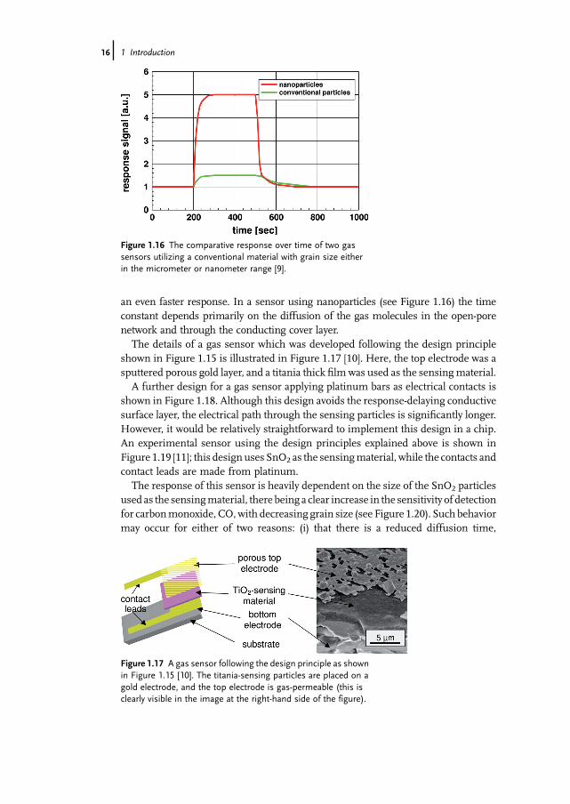
technically, the most important example being the gas sensor. This is based on theprinciple that changes in electric conductivity are caused by changes in the stoichi-ometry of oxides, variations of which are often observed for transition metals. Thegeneral design of such a sensor is shown in Figure 1.15.This type of gas sensor is set up on a conductive substrate on a carrier plate, and the
surface of the conductive layer covered completely with the oxide sensor nanoparticles.Typically, for this application, nanoparticles of TiO2, SnO2, Fe2O3 are used. A furtherconductive cover layer is then applied on top of the oxide particle; it is important thatthis uppermost layer is permeable to gases. A change in the oxygen potential in thesurrounding atmosphere causes a change in the stoichiometry of the oxide particles,whichmeans that the oxygen/metal ratio is changed. It is important that this process isreversible, as the oxides are selected to showa large change in their electric conductivityas they change stoichiometry. The response of a sensor made from conventionalmaterial with grains in the micrometer size range, compared to a sensor usingnanomaterials, is shown in Figure 1.16. Clearly, the response of the nanoparticlesensor is faster and the signal better but, according to Equation (1.4), onemight expect
Figure 1.15 The general layout of a gas sensor based on nano-particles. The sensor comprises a layer of sensing nanoparticlesplaced on a conductive substrate, and the whole systemis covered with a gas-permeable electrode. Time controlling isvia diffusion in the open pore network; the influence ofbulk diffusion through the grains is negligible.
1.2 Elementary Consequences of Small Particle Size j15
an even faster response. In a sensor using nanoparticles (see Figure 1.16) the timeconstant depends primarily on the diffusion of the gas molecules in the open-porenetwork and through the conducting cover layer.The details of a gas sensor which was developed following the design principle
shown in Figure 1.15 is illustrated in Figure 1.17 [10]. Here, the top electrode was asputtered porous gold layer, and a titania thick film was used as the sensingmaterial.A further design for a gas sensor applying platinum bars as electrical contacts is
shown in Figure 1.18. Although this design avoids the response-delaying conductivesurface layer, the electrical path through the sensing particles is significantly longer.However, it would be relatively straightforward to implement this design in a chip.An experimental sensor using the design principles explained above is shown inFigure 1.19 [11]; this design uses SnO2 as the sensingmaterial, while the contacts andcontact leads are made from platinum.The response of this sensor is heavily dependent on the size of the SnO2 particles
used as the sensingmaterial, there being a clear increase in the sensitivity of detectionfor carbonmonoxide, CO,with decreasing grain size (see Figure 1.20). Such behaviormay occur for either of two reasons: (i) that there is a reduced diffusion time,
Figure 1.17 A gas sensor following the design principle as shownin Figure 1.15 [10]. The titania-sensing particles are placed on agold electrode, and the top electrode is gas-permeable (this isclearly visible in the image at the right-hand side of the figure).
Figure 1.16 The comparative response over time of two gassensors utilizing a conventional material with grain size eitherin the micrometer or nanometer range [9].
16j 1 Introduction

Figure 1.18 A sensor design applying platinum bars as electricalcontacts. The sensing nanoparticles (e.g., SnO2) are locatedbetween these contacts. The molecules to be detected (in thisexample oxygen and carbon monoxide) are shaded dark and lightgray, respectively. (Note: Themolecules and nanoparticles are notdrawn to the same scale.)
Figure 1.19 A gas sensor in which a SnO2 thick film made fromnanoparticles is applied as the sensing element [11].
Figure 1.20 The sensitivity of CO determination of a gas sensordesigned according to Figure 1.6. A significant increase insensitivity is achieved with decreasing grain size [11].
1.2 Elementary Consequences of Small Particle Size j17

according to Equation (1.3); and (ii) that there is an enlarged surface, therebyaccelerating exchange with the surrounding atmosphere.For the successful operation of a thick-film sensor, it is a necessary prerequisite that
the sensing layer be prepared from nanoparticles consisting of a highly porousstructure that allows a relatively rapid diffusion of the gas to be sensed. A scanningelectron microscopy image of the characteristic structure of such a SnO2 thick-filmlayer is shown in Figure 1.21; the high porosity of the sensing thick-film layer, whichis required to facilitate rapid diffusion of the gas species, is clearly visible.Sensors based on this design are well suited for implementation in technical
systems, and the structure of electrical contacts at the surface of a chip and integrationinto a technical system is shown inFigure 1.22 [12]. This designuses, for example, Pt/SnO2 particles as the sensor for oxygen partial pressure, with the electrical conduc-tivity of the sensor layer increasing with increasing CO concentration at the surface.Such a system consists of many sensing cells, as depicted in Figure 1.22a. Thisprovides two possibilities: (i) by detecting the same signal inmore than one cell, thereis a possibility of improving the signal-to-noise ratio; (ii) the cells can be covered witha diffusion layer of varying composition and thickness; after calibration, this designallows an additional determination of the gas species.
Figure 1.22 Technical realization of a gas sensor according to adesign as depicted in Figure 1.18 [12]. (a) The sensing element ona chip. (b) An array of sensing elements; these arrays also allowidentification of the gas species (Reprinted with permission fromNIST Boulder Laboratories, Semoncik [12]).
Figure 1.21 The structure of a SnO2 thick-film layer (note the openstructure here) (Barunovic and Hahn, with kind permission [11]).
18j 1 Introduction

As mentioned above, it is possible to cover each sensing elements with a diffusionbarrier of different thickness and composed of silica or alumina. Depending on themolecule�s size, the time response for different elements depends on the thickness ofthe surface coating. After empirical calibration, such a design is capable of providingnot only theoxygenpotential but also information on the gas species. The integration ofmany sensor chips on one substrate (as shown in Figure 1.22b) opens the gate forfurther far-reaching possibilities, especially if the individual sensing elements arecoatedwith a secondmaterial of varying thickness [13,15], or if the sensingelementsaremaintained at different temperatures [14,15]. A typical example of the influence of acoating at the surface of the sensor is shown in Figure 1.23, where the sensor signal isplotted against the concentration of the gas to be determined (in this case, benzene andpropane). Because of the different sizes of these two molecules, the coating has anindividual influenceon the signal, and the subsequent useof somemathematics allowsthe gas species and its concentration to be determined. However, this approach isclearly valid only for those species where the calibration curves already exist.
References
1 Vollath, D. and Szabó, D.V. (2002) in:Innovative Processing of Films andNanocrystalline Powders, (ed. K-.L. Choi),Imperial College Press, London, UK,pp. 219–251.
2 Nanophase. Nanophase TechnologiesCorporation, Romeoville, IL. www.nanophase.com 2007.
3 MACH I, Inc. , King of Prussia, PA.www.machichemicals.com 2007.
4 Vollath, D. and Szabó, D.V. (1999) J.Nanoparticle Res., 1, 235–242.
5 Vollath, D. and Sickafus, K.E. (1992)unpublished results.
6 Vollath, D., Szabó, D.V. and Fuchs, J.(1999) Nanostructured Mater, 12, 433–438.
Figure 1.23 Calibration curves for bare and 10 nm SiO2-coatedgas sensors using SnO2 to prepare the sensing nanoparticles. Asthe influence of the coating is dependent on the gas species, thenature, concentrations and/or relative proportions of the twospecies can be determined [13].
References j19

7 Vollath, D. and Szabó, D.V. (1994)Nanostructured Mater, 4, 927–938.
8 Schumacher, S., Birringer, R., Strauß, R.and Gleiter, H. (1989) Acta Metall., 37,2485–2488.
9 ww.boulder.nist.gov/div853/Publication%20files/NIST_BCC_Nano_Hooker_2002.pdf.
10 Cho, Y.S. and Hahn, H. (2003) TechnicalUniversity Darmstadt, Germany privatecommunication.
11 Barunovic, R. and Hahn, H. (2003)Technical University Darmstadt, Germanyprivate communication.
12 Semoncik, S. (2007) NIST privatecommunication.
13 Althainz, P., Dahlke, A., Frietsch-Klarhof, M., Goschnick, J. and Ache,H.J. (1995) Sensors and Actuators B.,24–25, 366–369.
14 Althainz, P., Goschnick, J., Ehrmann, S.and Ache,H.J. (1996) Sensors and ActuatorsB., 33, 72–76.
15 Semoncik, S., Cavicchi, R.E., Wheeler, C.,Tiffong, J.E., Walton, R.M., Svehle, J.S.,Panchapakesau, B. and De Voe, D.L.(2007) Sensors and Actuators B., 77,579–591.
20j 1 Introduction
![1 General Properties of Nitrides - Wiley-VCH · cubic unit cell, containing four ... [0001] TT' {1100} 〈1120 ... 1 General Properties of Nitrides. The u parameter is defined as](https://img.pdfslide.net/doc/110x75/5ac229647f8b9a357e8d8518/1-general-properties-of-nitrides-wiley-unit-cell-containing-four-0001.jpg)