Embed Size (px)
Citation preview
1
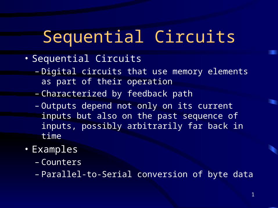
Sequential Circuits• Sequential Circuits
– Digital circuits that use memory elements as part of their operation
– Characterized by feedback path– Outputs depend not only on its current inputs but
also on the past sequence of inputs, possibly arbitrarily far back in time
• Examples– Counters– Parallel-to-Serial conversion of byte data
2
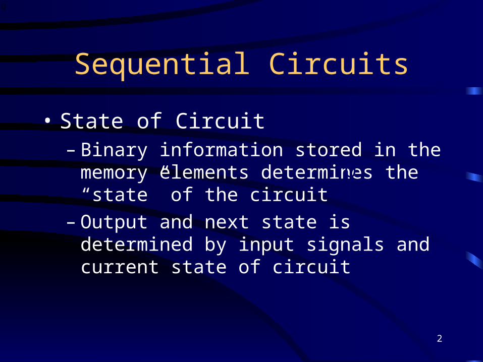
Sequential Circuits
• State of Circuit– Binary information stored in the memory
elements determines the “state” of the circuit– Output and next state is determined by input
signals and current state of circuit
Q
Q
3
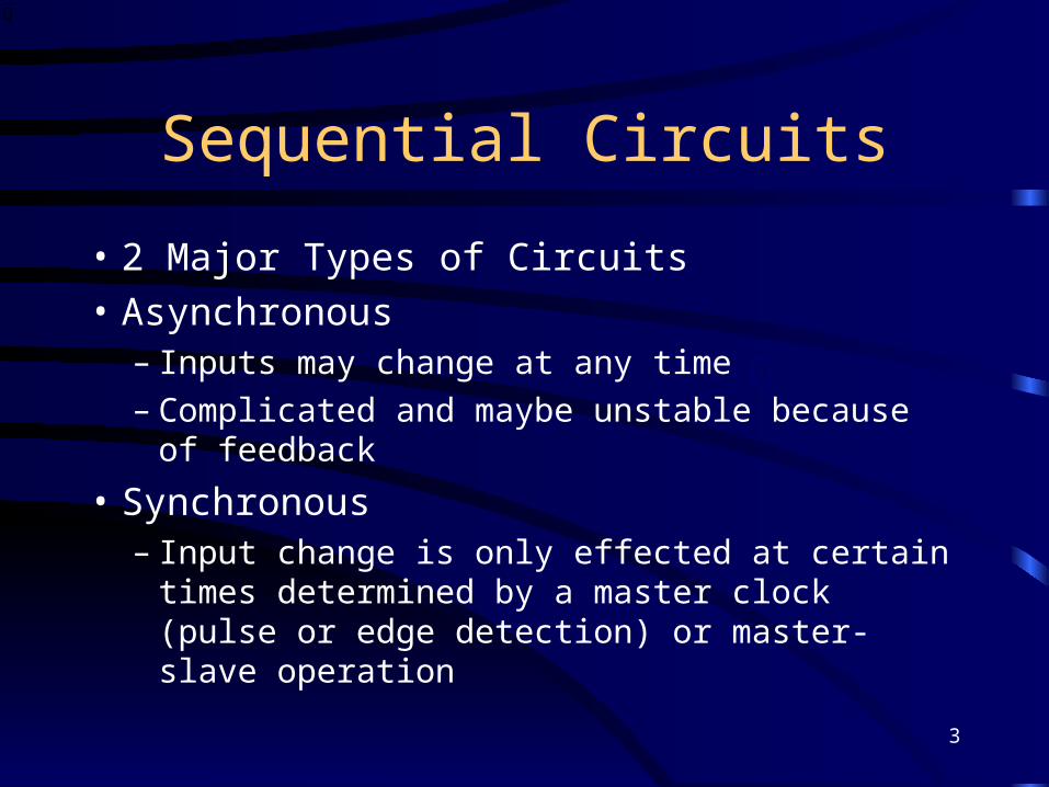
Sequential Circuits
• 2 Major Types of Circuits• Asynchronous
– Inputs may change at any time– Complicated and maybe unstable because of
feedback
• Synchronous– Input change is only effected at certain times
determined by a master clock (pulse or edge detection) or master-slave operation
Q
Q
4
Asynchronous Sequential Circuits
Latch• Temporary storage device that has two stable states• Normally has two inputs • Two complementary outputs available: Q and Q’• When the latch is set to a certain state it retains its
state unless the inputs are changed to set the latch to a new state
• A latch serves as a memory element which is able to retain the information stored in it
5
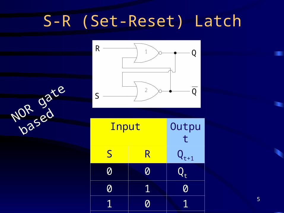
S-R (Set-Reset) Latch
1
2 Q
QR
S
Input Output
S R Qt+1
0 0 Qt
0 1 0
1 0 1
1 1 Invalid
NOR gate based
6
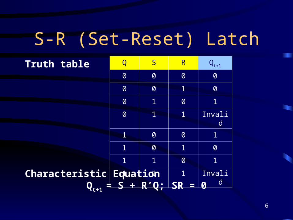
S-R (Set-Reset) LatchTruth table
Characteristic EquationQt+1 = S + R’Q; SR = 0
Q S R Qt+1
0 0 0 0
0 0 1 0
0 1 0 1
0 1 1 Invalid
1 0 0 1
1 0 1 0
1 1 0 1
1 1 1 Invalid
7
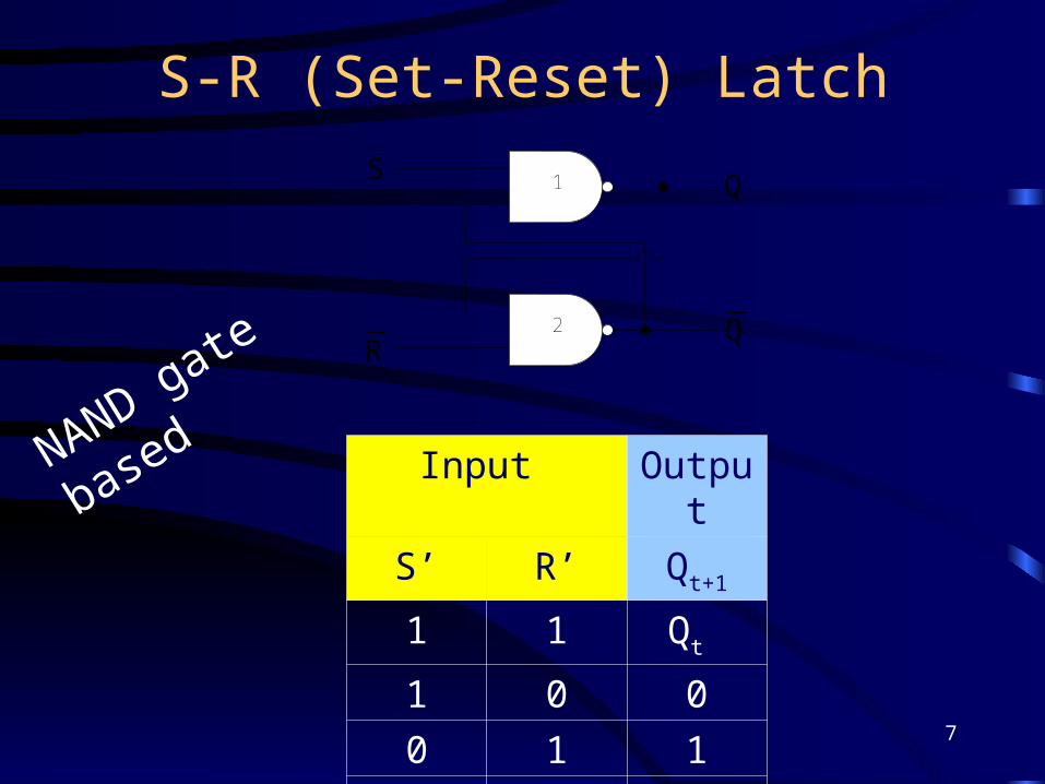
S-R (Set-Reset) Latch
Input Output
S’ R’ Qt+1
1 1 Qt
1 0 0
0 1 1
0 0 Invalid
NAND gate based
1
2 Q
S
R
Q
8
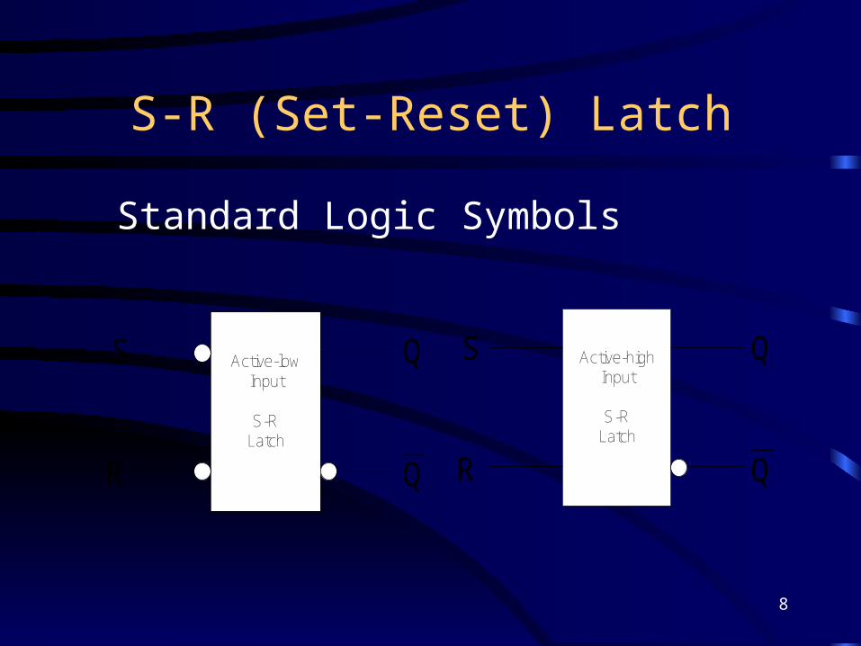
S-R (Set-Reset) Latch
Standard Logic Symbols
Active-highInput
S-RLatch
Q
QS
R
Active-lowInput
S-RLatch
Q
QS
R
9
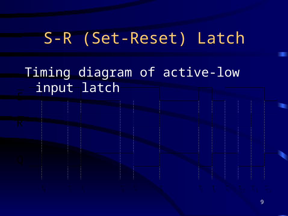
S-R (Set-Reset) Latch
Timing diagram of active-low input latch
S
R
Q
t1 t2 t3 t4 t5 t6 t7 t8 t9 t10 t11 t12
10
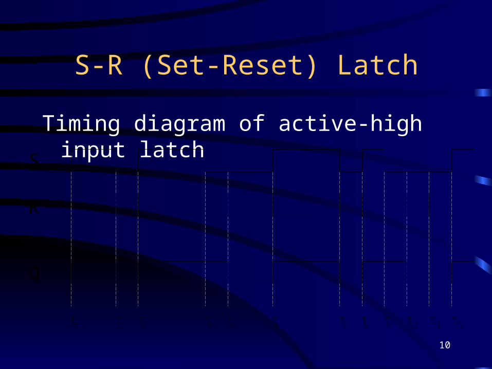
S-R (Set-Reset) Latch
Timing diagram of active-high input latch
S
R
Q
t1 t2 t3 t4 t5 t6 t7 t8 t9 t10 t11 t12
11
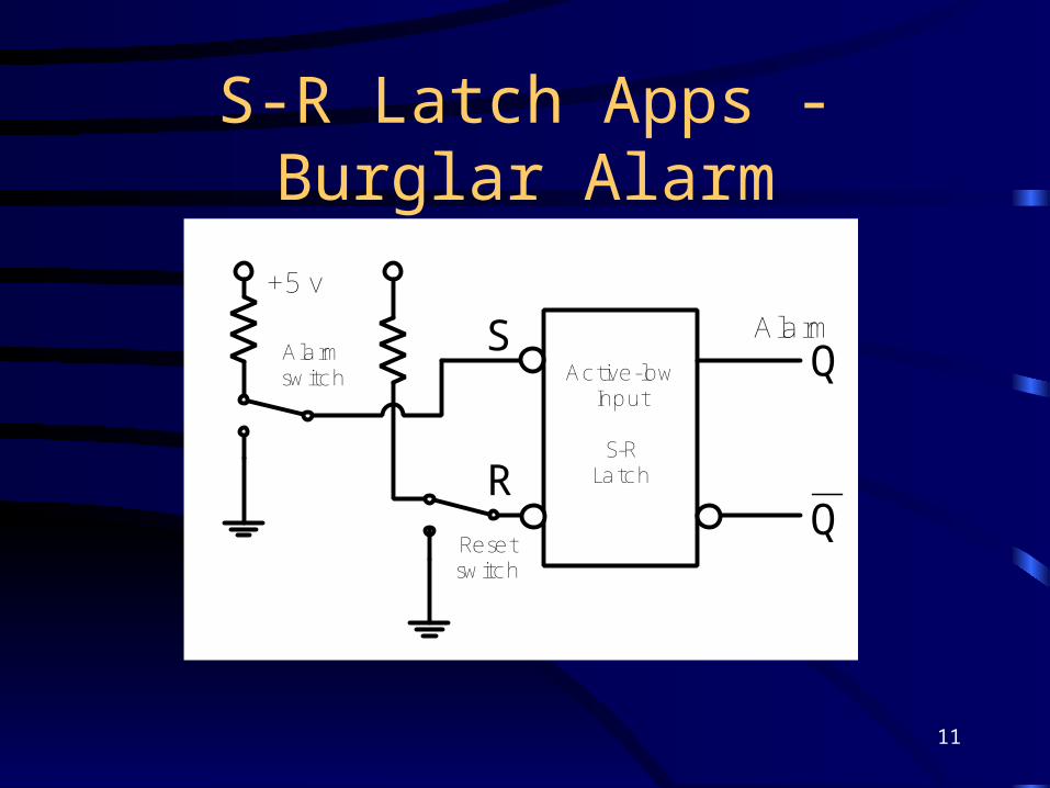
S-R Latch Apps - Burglar Alarm
Active-lowInput
S-RLatch
Q
QS
R
+5 v
Alarm
Reset switch
Alarm switch
12
Synchronous Sequential Circuits• Latches
– Asynchronous circuits– Outputs are transparent to inputs
• Gated or Clocked Latches– Synchronous circuits b/c clock or enable input dictates when
inputs are latched onto outputs– May still have both transparent and latched operation if inputs
change while clock is active• Flip Flops
– Flip-Flops are synchronous bi-stable devices, known as bi-stable multivibrators
– The output of the flip-flop can only change once by the applied inputs upon application of clock input
– Edge Triggered or Master Slave

13
S-R Gated Latch– Adds a clock (control) input gated to an S-R latch– S/R inputs are passed on to the latch portion
synchronised by the clock pulse– Also called Clocked S-R Latch
1
2 Q
S
R
Q3
4
CK
GatedS-R
Latch
Q
QS
R
ENCK
14
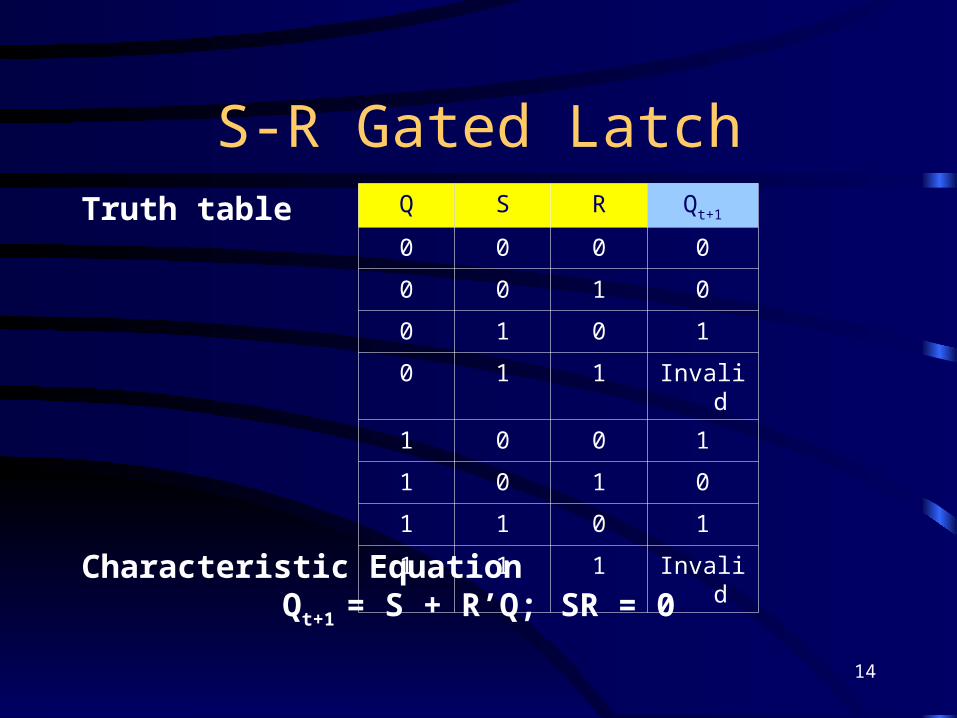
S-R Gated LatchTruth table
Characteristic EquationQt+1 = S + R’Q; SR = 0
Q S R Qt+1
0 0 0 0
0 0 1 0
0 1 0 1
0 1 1 Invalid
1 0 0 1
1 0 1 0
1 1 0 1
1 1 1 Invalid
15
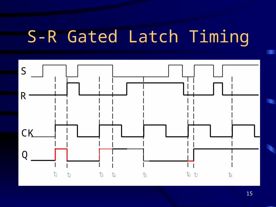
S-R Gated Latch Timing
S
R
Q
t1 t2 t3 t6t5
CK
t8t7t4
16
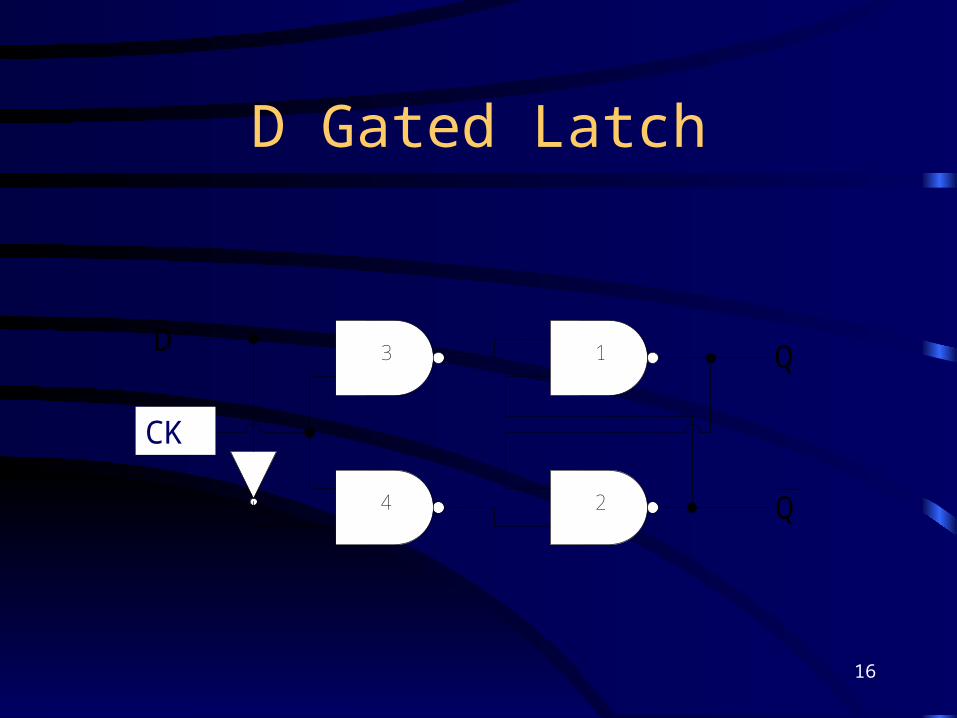
D Gated Latch
1
2 Q
D Q3
4
ENCK
17
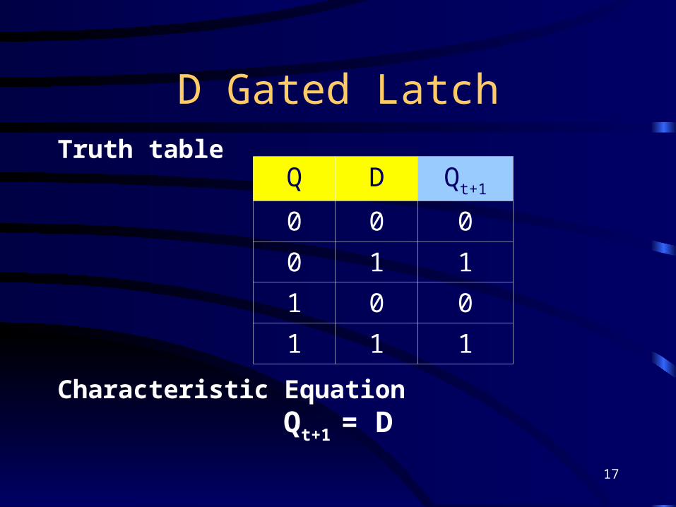
D Gated LatchTruth table
Characteristic EquationQt+1 = D
Q D Qt+1
0 0 0
0 1 1
1 0 0
1 1 1

18
D Gated Latch Apps
I01
I11
1I2
0I3
YEN
0
74X151
I40
I51
0I6
1I7
A0
A1
A2
C2
Counter
clock C1
C0
Serial Transmission
Line
D QEND QEND QEND QEND QEND QEND QEND QEN
1
1
1
0
0
1
0
1
19
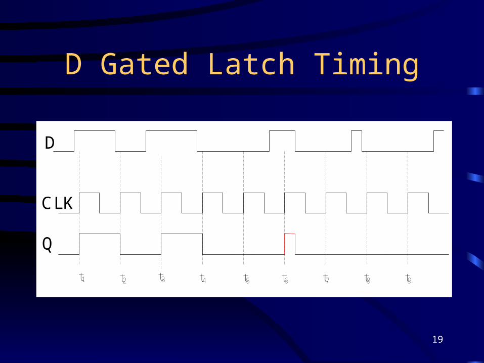
D Gated Latch Timing
D
Q
t1 t2 t3 t4 t5 t6 t7 t8 t9
CLK
20
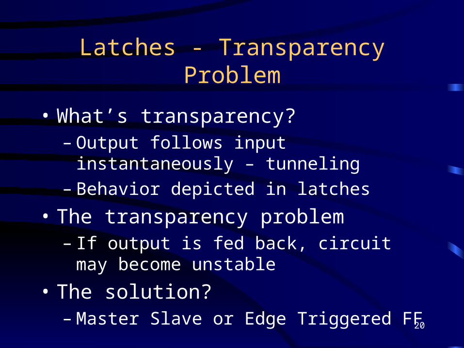
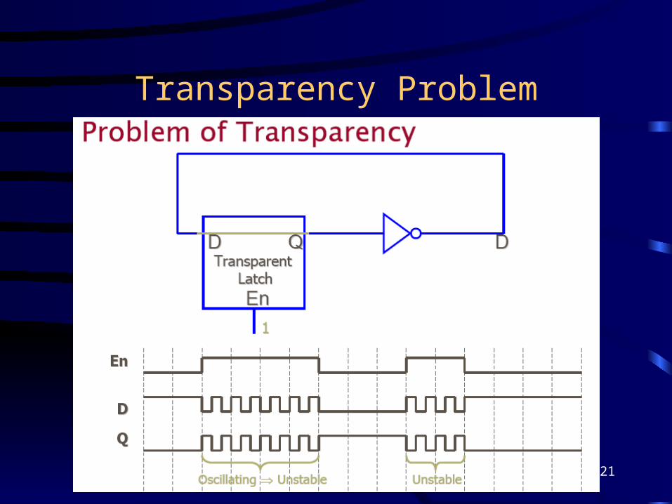
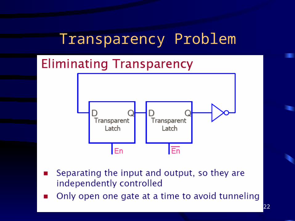
Latches - Transparency Problem
• What’s transparency?– Output follows input instantaneously –
tunneling– Behavior depicted in latches
• The transparency problem– If output is fed back, circuit may become
unstable
• The solution?– Master Slave or Edge Triggered FF
21
Transparency Problem
22
Transparency Problem

23
Master Slave Flip Flop
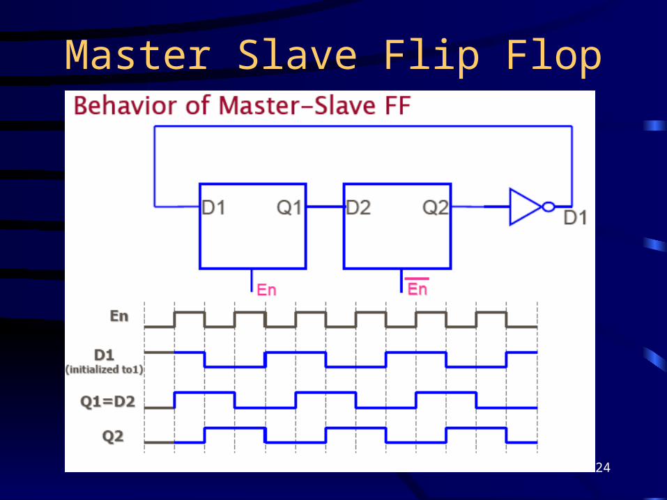
24
Master Slave Flip Flop
25
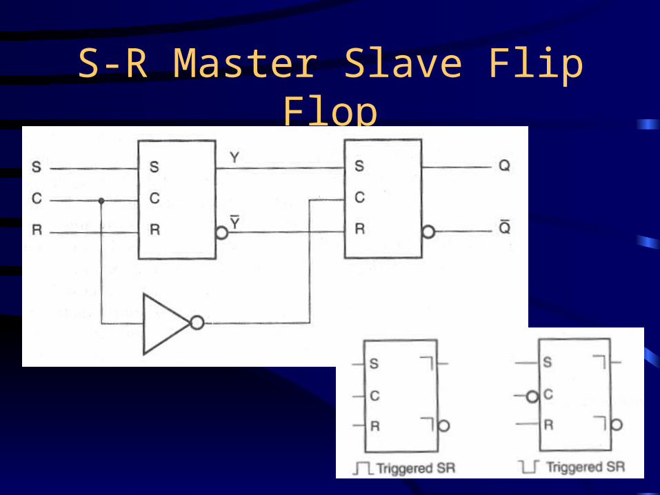
S-R Master Slave Flip Flop
26
Master Slave Flip Flops Summary• Have two stages – Master and Slave• Each stage works in one half of the clock signal• Inputs are applied in the first half of the clock signal• Outputs do not change until the second half of the clock
signal• Allows digital circuits to operate in synchronization with a
common clock signal• Inherently slow throughput• Mostly obsoleteBetter Solution:• Edge Triggered flip-flops• An edge-triggered flip-flop ignores the pulse while it is at
a constant level and triggers only during a transition of the clock signal - faster
27
D Flip-Flop Apps – Registers
Q
QSET
CLR
D
Q
QSET
CLR
D
Q
QSET
CLR
D
Q
QSET
CLR
D
D0
D1
D2
D3
Q0
Q1
Q2
Q3
CLK
Con
nect
ed to
inpu
ts o
f Mul
tiple
xer
D0
D1
D2
D3
Q0
Q1
Q2
Q3
CLK
t1
28
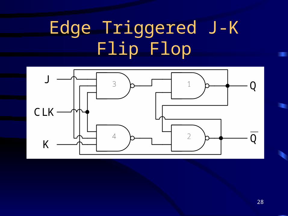
Edge Triggered J-K Flip Flop
1
2 Q
J
K
Q3
4
CLK
29
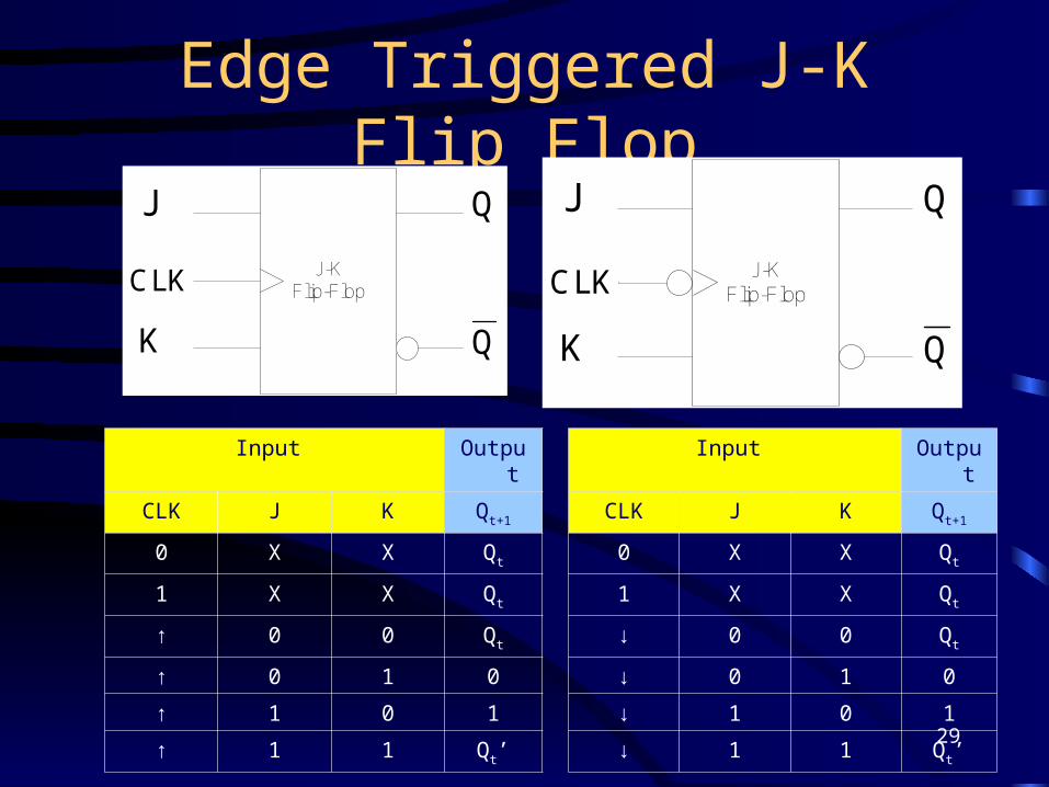
Edge Triggered J-K Flip Flop
tQ
J-KFlip-Flop
J
K
CLK
Q
Q
J-KFlip-Flop
J
K
CLK
Q
Q
Input Output
CLK J K Qt+1
0 X X Qt
1 X X Qt
↑ 0 0 Qt
↑ 0 1 0
↑ 1 0 1
↑ 1 1 Qt’
Input Output
CLK J K Qt+1
0 X X Qt
1 X X Qt
↓ 0 0 Qt
↓ 0 1 0
↓ 1 0 1
↓ 1 1 Qt’

30
T Flip FlopTruth table
Characteristic EquationQt+1 = TQ’ + T’Q
Q T Qt+1
0 0 0
0 1 1
1 0 1
1 1 0
31
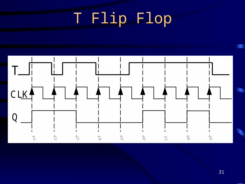
T Flip Flop
T
Q
t1 t2 t3 t4 t5 t6 t7 t8 t9
CLK

32
Flip-Flop Operating Characteristics
• Performance specified by several operating characteristics provided in the data sheets of FF’s
• The important operating characteristics are:– Propagation Delay
– Set-up Time
– Hold Time
– Maximum Clock frequency
– Pulse Width
– Power Dissipation

33
Flip Flop Logic Symbols Summary
34
Qt+1 = S + R’Q; SR = 0
Qt+1 = D
Qt+1 = JQ’ + K’Q
Qt+1 = TQ’ + T’Q
Flip Flop Characteristic Equations
35
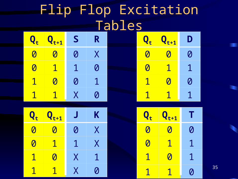
Flip Flop Excitation Tables
Qt Qt+1 S R
0 0 0 X
0 1 1 0
1 0 0 1
1 1 X 0
Qt Qt+1 J K
0 0 0 X
0 1 1 X
1 0 X 1
1 1 X 0
Qt Qt+1 D
0 0 0
0 1 1
1 0 0
1 1 1
Qt Qt+1 T
0 0 0
0 1 1
1 0 1
1 1 0
36
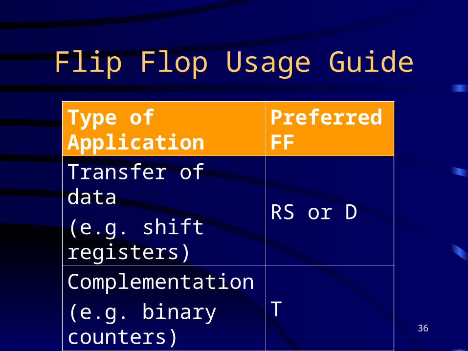
Flip Flop Usage Guide
Type of Application Preferred FF
Transfer of data
(e.g. shift registers)RS or D
Complementation
(e.g. binary counters)T
Above or any other
general applicationJK