Embed Size (px)
Citation preview
1
Simulation of Light-Emitting Simulation of Light-Emitting Diodes and Solar CellsDiodes and Solar Cells
Yen-Kuang Kuo, Jih-Yuan Chang, Miao-Chan Tsai,
Tsun-Hsin Wang, Yi-An Chang, Fang-Ming Chen,
and Shan-Rong Li
Department of Physics, College of Science
National Changhua University of Education
OPTIC 2013OPTIC 2013

2
Introduction III-nitride Light-emitting diodes (LEDs) III-nitride solar cells
Recent research results 1. Blue InGaN based LEDs
2. Green InGaN based LEDs
3. Ultraviolet AlInGaN based LEDs
4. Dual-wavelength emission LEDs
5. Superlattice solar cells
6. GaN-based Tunnel Junctions (TJ) Conclusion
Outline
3
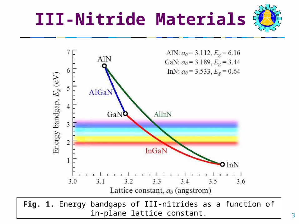
III-Nitride Materials
Fig. 1. Energy bandgaps of III-nitrides as a function of in-plane lattice constant.

4
III-Nitride LEDs
Sapphire (100 μm)
u-GaN
n-GaN
InGaN/GaN (MQW)
p-AlGaN (EBL)
p-GaN
p-contact
n-contact
Fig. 2. Schematic plot of the GaN-based LED structure.
Fig. 3. Schematic plot of the energy band diagrams.
GaN-based LEDs have extensive applications in full-color displays, liquid-crystal display backlighting, and solid-state illumination.
The LED market expands quickly due to many advantages, such as low-power consumption, long lifetime, and small size.

5
III-Nitride Solar Cells
Sapphire (100 μm)
u-GaN
n-GaN
InGaN(absorption layer)
p-GaN
p-contact
n-contact
Fig. 4. Schematic plot of the GaN-based solar cell structure.
Fig. 5. Schematic plot of the energy band diagrams.
The energy bandgap of InGaN alloys can cover most of the solar spectrum.
Many superior photovoltaic (PV) characteristics: high absorption coefficient, high carrier mobility, high saturation velocity, and high radiation resistance.
+
–
hν
p
n
Built-in field
Eg
Solar Irradiation

6
(Opt. Lett., vol. 38, p. 3158, 2013)
Numerical Study of the Suppressed Efficiency Droop in Blue InGaN LEDs
with Polarization-Matched Configuration
Recent research result No. 1

7
In blue InGaN LEDs, the Auger recombination can be reduced by reducing the carrier density.
Increasing the number of quantum wells (QWs) and thickening the width of wells, suffer from nonuniform carrier distribution and more severe spatial separation of electron and hole wave functions.
The severe quantum-confined Stark effect (QCSE) will reduce the radiative efficiency and hence cause an overall reduction in IQE.
Fig. 1. Band profiles and subband wave functions of the InGaN QWs with (a) 2.5 nm and (b) 5.0 nm widths, (c), (d) carrier concentrations and (e), (f) recombination rates of the 5.0 nm QW LED with two and six QWs at 100 A∕cm2.
Fig. 2. IQEs of the original LED structure with six QWs (QW width is 2.5 nm) and of the 5.0 nm QW LED with two and six QWs.

The purpose of reducing the number of quantum wells is to mitigate the additional compressive strain in polarization matched AlGaInN barriers. With the proposed LED structure, the QCSE can be markedly eliminated.
Moreover, the Auger recombination can also be largely suppressed as a result of the uniformly distributed and dispersed carriers. The IQE and the efficiency droop can thus be largely improved. 8
Fig. 3. (a) Band profile of the LED with two 5.0 nm thick polarization-matched QWs at 100 A∕cm2. (b) Enlarged drawing of the first QW in (a), in which the subband wave functions (C1 and HH1) are included. Band profile and subband wave functions (c) C1 and HH1 and (d) C2 and HH2 of the LED with a single 10.0 nm thick polarization-matched well at 100 A∕cm2.
Fig. 4. IQE characteristics of the original six-QW LED (QW width is 2.5 nm) and the LEDs with two 5.0 nm thick QWs and a single 10.0 nm thick polarization-matched well.

9
(Appl. Phys. Lett., vol. 100, p. 251102, 2013 )
Investigation of Green InGaN Light-Emitting Diodes with Asymmetric AlGaN
Composition-Graded Barriers and without an Electron Blocking Layer
Recent research result No. 2

10
The characteristics of the green InGaN LEDs with asymmetric AlGaN CGBs and without the commonly used AlGaN EBL are systematically investigated.
Green InGaN LEDs with asymmetric AlGaN composition-graded barriers and without the use of an AlGaN electron blocking layer is presented to possess markedly enhanced optical and electrical performance.
Fig. 1. Schematic plot of the green LEDs under study. Structure A is a conventional green LED. Structure B has identical layer structure with structure A except that the GaN barriers are replaced by asymmetric AlGaN CGBs. Structure C has identical layer structure with structure B except that the AlGaN EBL is removed.
Fig. 2. Simulated L-I-V characteristics and IQEs as a function of injection current for the three LEDs.
Al compositions in AlGaN barriers:13-11%, 11-9%, 9-7%, 7-5%, 5-3%,3-1%, 1-0%
= 508 nm6 QWs

11
Specifically, the energy band diagrams, carrier transportation, and distribution in the active region are studied.
It is observed in Figs. 3 (b) and 3 (c) that the energy bands become flatter, electrons can be confined in the active region more effectively, and holes can be injected into the active region more easily, especially when the LED is with the asymmetric AlGaN CGBs and without an AlGaN EBL.
The simulation results suggest that the improved device performance is due mainly to the markedly enhanced injection of holes into the active region.
Fig. 3. Energy band diagrams near the active region of the three LEDs at 100 mA.
Fig. 4. Carrier concentrations near the active regions of the three LEDs at 100 mA.

12
(IEEE J. Quantum Electron., vol. 49, p. 553, 2013 )
Design and Characterization of Polarization-Reversed AlInGaN Based
Ultraviolet Light-Emitting Diode
Recent research result No. 3
13
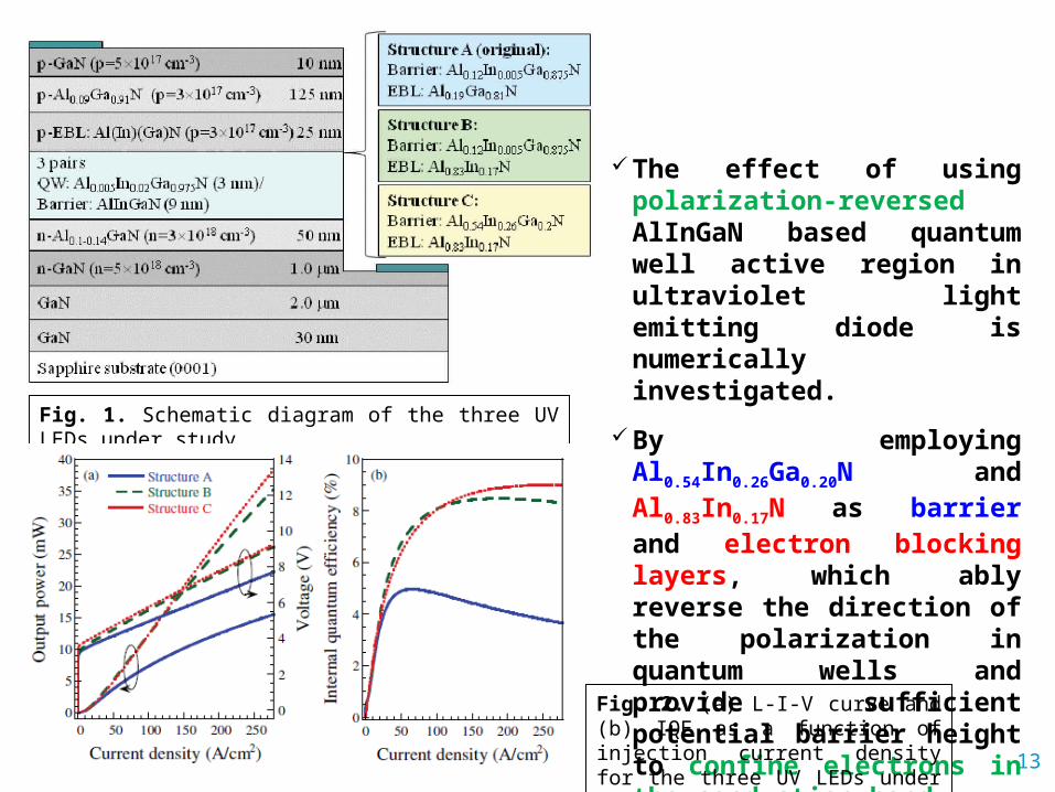
The effect of using polarization-reversed AlInGaN based quantum well active region in ultraviolet light emitting diode is numerically investigated.
By employing Al0.54In0.26Ga0.20N and Al0.83In0.17N as barrier and electron blocking layers, which ably reverse the direction of the polarization in quantum wells and provide sufficient potential barrier height to confine electrons in the conduction band.
Fig. 1. Schematic diagram of the three UV LEDs under study.
Fig. 2. (a) L-I-V curve and (b) IQE as a function of injection current density for the three UV LEDs under study.
14
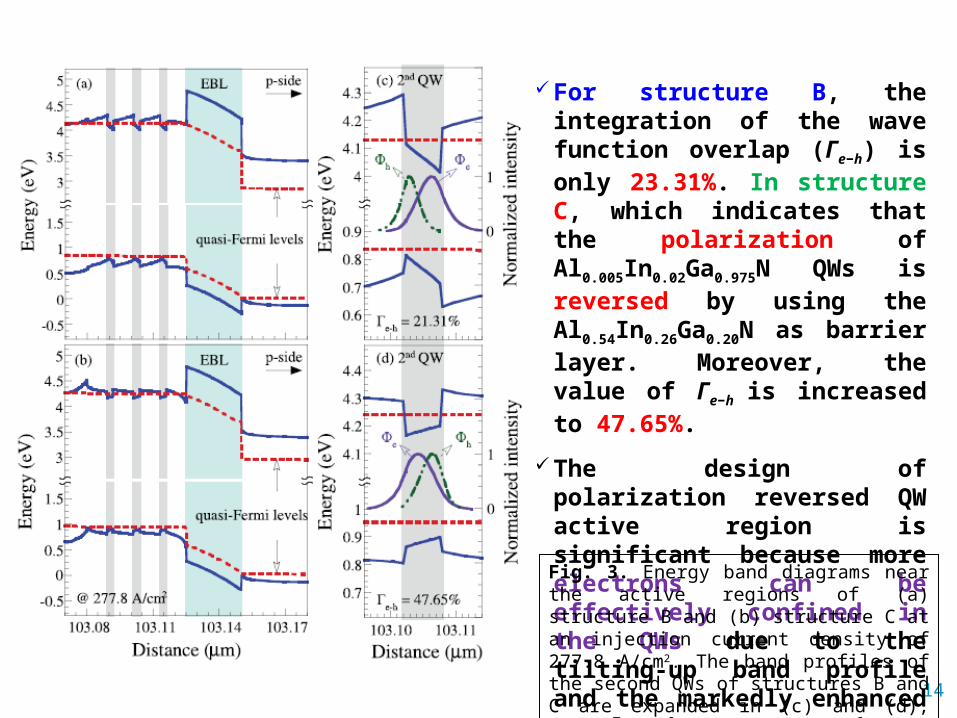
For structure B, the integration of the wave function overlap (Γe−h) is only 23.31%. In structure C, which indicates that the polarization of Al0.005In0.02Ga0.975N QWs is reversed by using the Al0.54In0.26Ga0.20N as barrier layer. Moreover, the value of Γe−h is increased to 47.65%.
The design of polarization reversed QW active region is significant because more electrons can be effectively confined in the QWs due to the tilting-up band profile and the markedly enhanced overlap between Φe and Φh.
Fig. 3. Energy band diagrams near the active regions of (a) structure B and (b) structure C at an injection current density of 277.8 A/cm2. The band profiles of the second QWs of structures B and C are expanded in (c) and (d), respectively.

15
It is observed that more carriers are confined in the QWs, which contributes to the radiative recombination more efficiently since the electron leakage current is suppressed markedly when the original Al0.19Ga0.81N EBL is replaced by a high-bandgap Al0.83In0.17N layer in structures B and C. Fewer carriers are confined in the QWs of structure A, which in turn results in the lowest radiative and Auger recombinations.
Fig. 4. (a) Percentage of electron leakage current. (b) Integrated Auger recombination rate distributed in the QWs as a function of injection current density for the three UV LEDs under study. The insets of (a) and (b) show the normalized current density flowing along the growth direction near the active region and the Auger recombination rate distributed in the QWs, respectively, when the injection current density is 277.8 A/cm2.

16
(Appl. Phys. Lett., vol. 102, p. 171112, 2013 )
Spectral Competition of Chirped Dual-Wavelength Emission in Monolithic InGaN
Multiple-Quantum Well Light-Emitting Diodes
Recent research result No. 4

17
In this work, spectral competition of chirped dual-wavelength emission in monolithic InGaN MQW LEDs is studied numerically.
In addition to the crystalline quality that is generally desired for good LED performance, the simulation results show that effective suppression of piezoelectric polarization is another key issue toward the realization of efficient monolithic dual-wavelength emission in InGaN MQW LEDs.Fig. 1. Schematic diagrams of green-violet LED, violet-green
LED, strain reduced LED, and broad-band LED.

18
The green-violet LED suffers from large polarization field induced by the large polarization mismatch between the green QWs and GaN barriers and thus the insufficient injection efficiency of holes in green QWs near n-side is detrimental for spectral balance and the realization of dual-wavelength emission.
For the violet-green LED, the injection efficiency of holes in the green QWs is improved with the price of reduced injection efficiency of holes in the violet QWs.
The strain-reduced LED relaxes the strain between the QWs and barriers effectively, which results in a flatter band diagram, the phenomenon of insufficient injection of holes still exists.
For broad-band LED, the first QW near n-side cannot contribute to spontaneous emission effectively; however, the reduced band-bending phenomenon is beneficial for the injection of holes in both green QWs and violet QWs.
Fig. 2. Energy band diagrams near the active region of (a) green-violet LED, (b) violet-green LED, (c) strain-reduced LED, and (d) broad-band LED at 100 mA.

19
For green-violet LED, the spontaneous emission rates of green QWs and violet QWs increase simultaneously with the increase of injection current.
For the violet-green LED with reversed sequence of QWs, although the spontaneous emission of green QWs is enhanced by moving the green QWs toward the p-side, the light output from the violet QWs deteriorates seriously and hence only green emission.
The total light output of the strain-reduced LED is improved compared to that of the green-violet LED; however, the spontaneous emission of green QWs is always higher than that of violet ones, which indicates that the carriers distributed in the dual-wavelength QWs are not balanced.
For the broad-band LED, the green QWs and violet QWs have similar emission performance and approximately equal intensity of the dual-wavelength emission is achieved at 100 mA.
Fig. 3. Energy band diagrams near the active region of (a) green-violet LED, (b) violet-green LED, (c) strain-reduced LED, and (d) broad-band LED at 100 mA.

20
Recent research result No. 5
(IEEE Photonics Technol. Lett., vol. 25, p. 85, 2013)
Advantages of InGaN Solar Cells with P-doped and High-Al-Content Superlattice AlGaN Barriers

21
When the In content in InGaN QWs is increased from 21% to 40%, the conversion efficiency can be increased from 1.13% to 1.38%.
The improvements in the In0.4Ga0.6N/Al0.14Ga0.86N SL solar cell can be attributed to the markedly increased Jsc by increasing In content in InGaN QWs for long wavelength absorption, although the Voc is reduced accordingly.
Meanwhile, since the depth of the In0.4Ga0.6N QWs becomes deeper, the carriers generated by the photon absorption in In0.4Ga0.6N QWs are relatively difficult to escape.
By introducing p-type doping in Al0.14Ga0.86N barriers, it is noted worthily that the Jsc can be further enhanced to 1.82 mA/cm2, the FF can also be slightly improved, and accordingly the conversion efficiency is increased to 1.65%.
Fig. 1. Experimental and simulated photovoltaic J-V characteristics of the In0.21Ga0.79N and In0.4Ga0.6N SL solar cells with undoped and p-type doped Al0.14Ga0.86N barriers under AM 1.5 G illumination.
14-pair SL

22
The simulation results suggest that the conversion efficiency can be markedly enhanced by introducing p-type doping and more Al content in AlGaN barriers, which is mainly attributed to the improved capability of carrier transport, hence increasing the carrier collection efficiency.
Fig. 2. Photovoltaic J-V characteristics of the In0.4Ga0.6N SL solar cells with undoped Al0.14Ga0.86N, undoped and p-type doped Al0.2Ga0.8N barriers under AM 1.5 G illumination.
Fig. 3. Electron and hole current densities distributed in the In0.4Ga0.6N SL solar cells with undoped Al0.14Ga0.86N, undoped and p-type doped Al0.2Ga0.8N barriers.

23
Recent research result No. 6
(IEEE J. Lightwave Technol., vol. 31, p. 3575, 2013)
Low Resistivity GaN-Based Polarization-Induced Tunnel Junctions

24
The TJ resistivity can be reduced from the original value of 69.6 Ω·cm2 down to 7.8 × 10⁻³ Ω·cm2 (which is needed for a reasonable voltage drop of <0.3 V) by the introduction of several functional layers.
Fig. 1. (a) Schematic diagram of the n-i-p TJ for simulation (refer to T1). J–V curves in log scale of different TJ structures showing the dependence on (b) InGaN composition and (c) thickness of the i-layer.
Performance of TJ Structure as a Function of InGaN Composition and Thickness of the I-layer (T1)
(a)
High InDefectsOptical absorptionIn = 0.2
2,3 nm

(a)
25
Firstly, inserting two thin (5 nm) highly-doped p- and n-GaN layers below and above the InGaN layer to support more space charges.
With 5 nm layers of p-GaN and n-GaN with [ND ] = 3 × 1019 cm−3 and [NA] = 2 × 1019 cm−3 (denoted as T2), the resistivity of the TJ is reduced to 5 × 10⁻² Ω·cm2.
Further increasing the Mg doping level from 2 to 3 × 1019 cm−3 does not increase the tunneling current appreciably, while increasing the Si doping changes the current density by almost an order of magnitude. Because of the large conduction band offset of the nitride materials, increasing the Si doping density is more effective than increasing the Mg doping density for improving the tunneling.
Fig. 2. (a) Schematic diagram of the n-i-p TJ with the insertion of thin layers of different doping levels (refer to T2). (b) J–V curves in log scale.
Dependence on [Mg] and [Si] Doping Densities (T2)
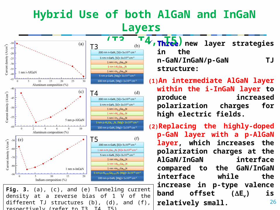
26
ThreeThree new layer strategies in the n-GaN/InGaN/p-GaN TJ structure:
(1) An intermediate AlGaN layer within the i-InGaN layer to produce increased polarization charges for high electric fields.
(2) Replacing the highly-doped p-GaN layer with a p-AlGaN layer, which increases the polarization charges at the AlGaN/InGaN interface compared to the GaN/InGaN interface while the increase in p-type valence band offset (Ev) is relatively small.
(3) Utilization of InGaN as the n-type layer, in which the decrease in the n-type conduction band energy is effective for shallow well trapping of charge carriers for tunneling.
Fig. 3. (a), (c), and (e) Tunneling current density at a reverse bias of 1 V of the different TJ structures (b), (d), and (f), respectively (refer to T3, T4, T5).
Hybrid Use of both AlGaN and InGaN Layers (T3, T4, T5)
T3
T4
T5
27
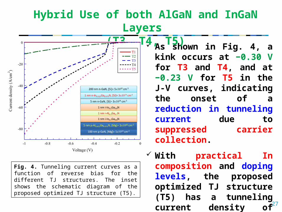
As shown in Fig. 4, a kink occurs at −0.30 V for T3 and T4, and at −0.23 V for T5 in the J-V curves, indicating the onset of a reduction in tunneling current due to suppressed carrier collection.
With practical In composition and doping levels, the proposed optimized TJ structure (T5) has a tunneling current density of more than 80 A/cm2 at –1 V and a resistivity of as low as 7.8 × 10⁻³ Ω·cm2.
Fig. 4. Tunneling current curves as a function of reverse bias for the different TJ structures. The inset shows the schematic diagram of the proposed optimized TJ structure (T5).
Hybrid Use of both AlGaN and InGaN Layers (T3, T4, T5)

28
1. Some specific designs on band structure near the active region in the blue, green, UV, and dual-wavelength LEDs are investigated with the APSYS simulation program.
2. Simulation results show that, with appropriate designs, the optical performance may be effectively improved due to the increase of hole injection efficiency, enhancement of electron confinement, or uniform distribution of carriers in the active region.
3. Some specific methods may also be employed in III-nitride solar cells to enhance the device performance.
4. The tunnel junction design principles introduced here may enable a new range of high efficiency GaN-based devices, such as the enhanced multijunction solar cells, optoelectronic and electronic devices.
Conclusion

29
More papers in 2013 Jih-Yuan Chang, Shih-Hsun Yen, Yi-An Chang, and Yen-Kuang
Kuo*, “Simulation of high-efficiency GaN/InGaN p-i-n solar cell with suppressed polarization and barrier effects,” IEEE Journal of Quantum Electronics, Vol. 49, No. 1, 17–23, January 2013.
Jih-Yuan Chang, Shih-Hsun Yen, Yi-An Chang, Bo-Ting Liou, and Yen-Kuang Kuo*, “Numerical investigation of high efficiency InGaN-based multi-junction solar cell,” IEEE Transactions on Electron Devices, Vol. 60, No. 12, pp. 4140–4145, December 2013.
Jih-Yuan Chang, Yi-An Chang, Fang-Ming Chen, Yih-Ting Kuo, and Yen-Kuang Kuo*, “Improved quantum efficiency in green InGaN light-emitting diodes with InGaN barriers,” IEEE Photonics Technology Letters, Vol. 25, No. 1, 55–58, January 2013.
Jih-Yuan Chang and Yen-Kuang Kuo*, “Advantages of blue InGaN light-emitting diodes with composition-graded barriers and electron-blocking layer,” Physica Status Solidi (a), Vol. 210, No. 6, 1103–1106, published online 12 February 2013.

30
Some of Our Previous Papers
Yen-Kuang Kuo*, Tsun-Hsin Wang, and Jih-Yuan Chang, “Advantages of InGaN light-emitting diodes with InGaN-AlGaN-InGaN barriers,” Applied Physics Letters, Vol. 100, No. 3, 031112, 2012. (Editor's choice: one of the Best Papers of 2012)
Yen-Kuang Kuo*, Jih-Yuan Chang, Miao-Chan Tsai, and Sheng-Horng Yen, “Advantages of blue InGaN multiple-quantum well light-emitting diodes with InGaN barriers,” Applied Physics Letters, Vol. 95, No. 1, 011116, 2009. (High-download and highly cited paper)
31
Thank you for your attention!
Blue Laser Lab, NCUE, Taiwan