Embed Size (px)
Citation preview

Bipolar and Field Eff ect Transistors
Learning Outcomes
This chapter deals with the construction and operating characteristics of transistors, depending upon how they are connected into a circuit. The basics of semiconductor materials and their application to diodes is covered in Fundamental Electrical and Electronic Principles , ISBN 9780750687379, 2008, Chapter 9.
11
1 The Bipolar Junction Transistor (BJT)
This is a three-layer device where the semiconductor is doped so as to produce a ‘ sandwich ’ of either two n-type layers with a p-type layer between them, or two p-type layers with an n-type layer between them. The former is known as an npn transistor and the latter as a pnp transistor. The term bipolar refers to the fact that conduction within the device is due to the movement of both positive and negative charge carriers (holes and electrons). Both forms of BJT are illustrated in Fig. 1.
From Fig. 1 it may be seen that the transistor has two p-n junctions, each of which will have the same characteristics as a p-n junction diode. The middle layer of the ‘ sandwich ’ is much narrower and more lightly doped than the two outer layers.
(a) npn (b) pnp
Fig. 1
WEBA-CHAP2.indd 11 5/2/2008 3:10:18 PM

12 Bipolar and Field Eff ect Transistors
Since the device has three layers then it is possible to make three electrical connections to it, i.e it is a three-terminal device. In addition, it is possible to connect external sources of emf so as to either forward or reverse bias the two internal p-n junctions. The three layers are named the emitter, base and collector, and the action of an npn transistor is illustrated in Fig. 2.
IE
IC
IB
B1
B2
baseemitter collector
ELECTRONS
Fig. 2
Battery B 1 forward biases the emitter-base junction (positive to ‘ p ’ and negative to ‘ n ’ ), whilst the collector-base junction is reversed biased by battery B 2. The effect of B 1 is to accelerate free electrons from the emitter towards the base. Since the base region is relatively narrow and lightly doped, the vast majority (over 95%) of these electrons will pass straight through the base and cross the second junction into the collector region. Once they reach the collector they will be attracted by the positive potential provided by battery B 2 , and fl ow to this battery. The small percentage of the emitter electrons that recombine with holes in the base will be replaced by electron-hole pairs, the electrons from which will leave the base and fl ow out to the positive plate of B 1 . Applying Kirchhoff ’ s current law to the circuit it may be seen that
I I IE C B� � amp (1)
This equation will always hold true regardless of the way in which the transistor is connected into a circuit, and could be said to describe normal transistor action. It may also be seen that in Fig. 2 the connection to the base is a common point in the external circuit, and when the transistor is connected in this way it is said to be connected in the common base confi guration.
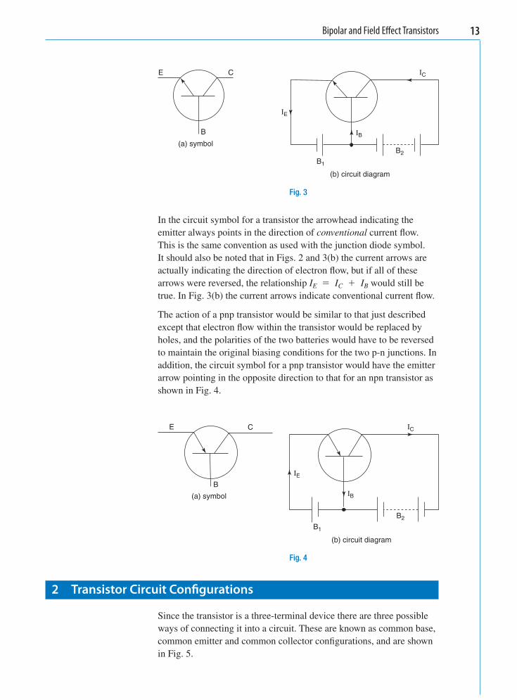
For obvious reasons, the depiction of the transistor in the form of Fig. 2 is not convenient when drawing circuit diagrams, and the circuit symbol for an npn transistor and its use for the circuit of Fig. 2 are shown in Fig. 3 .
WEBA-CHAP2.indd 12 5/2/2008 3:10:19 PM
Bipolar and Field Eff ect Transistors 13
In the circuit symbol for a transistor the arrowhead indicating the emitter always points in the direction of conventional current fl ow. This is the same convention as used with the junction diode symbol. It should also be noted that in Figs. 2 and 3(b) the current arrows are actually indicating the direction of electron fl ow, but if all of these arrows were reversed, the relationship I E � I C � I B would still be true. In Fig. 3(b) the current arrows indicate conventional current fl ow.
The action of a pnp transistor would be similar to that just described except that electron fl ow within the transistor would be replaced by holes, and the polarities of the two batteries would have to be reversed to maintain the original biasing conditions for the two p-n junctions. In addition, the circuit symbol for a pnp transistor would have the emitter arrow pointing in the opposite direction to that for an npn transistor as shown in Fig. 4 .
E C
B
(a) symbol
(b) circuit diagram
IE
IB
B1
B2
IC
Fig. 3
E
(a) symbol
C
B
(b) circuit diagram
IC
IB
IE
B1
B2
Fig. 4
2 Transistor Circuit Confi gurations
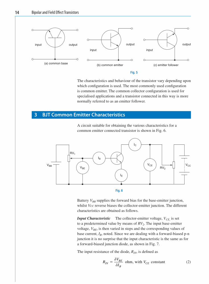
Since the transistor is a three-terminal device there are three possible ways of connecting it into a circuit. These are known as common base, common emitter and common collector confi gurations, and are shown in Fig. 5 .
WEBA-CHAP2.indd 13 5/2/2008 3:10:19 PM
14 Bipolar and Field Eff ect Transistors
The characteristics and behaviour of the transistor vary depending upon which confi guration is used. The most commonly used confi guration is common emitter. The common collector confi guration is used for specialised applications and a transistor connected in this way is more normally referred to as an emitter follower.
3 BJT Common Emitter Characteristics
A circuit suitable for obtaining the various characteristics for a common emitter connected transistor is shown in Fig. 6 .
(a) common base
input output
(b) common emitter
input
output
(c) emitter follower
input
output
Fig. 5
VBB VBE
VCE VCC
IB
IE
IC
RV1
RV2
Fig. 6
Battery V BB supplies the forward bias for the base-emitter junction, whilst Vcc reverse biases the collector-emitter junction. The different characteristics are obtained as follows.
Input Characteristic The collector-emitter voltage, V CE , is set to a predetermined value by means of RV 2. The input base-emitter voltage, V BE , is then varied in steps and the corresponding values of base current, I B , noted. Since we are dealing with a forward-biased p-n junction it is no surprise that the input characteristic is the same as for a forward-biased junction diode, as shown in Fig. 7 .
The input resistance of the diode, R IN, is defi ned as
R
V
IVIN
BE
BCE�
��
ohm, with constant
(2)
WEBA-CHAP2.indd 14 5/2/2008 3:10:21 PM

Bipolar and Field Eff ect Transistors 15
A typical value for R IN would be between 1000 and 1500 ohm.
Output Characteristics For this test I B is set to a fi xed value using RV 1 ; V CE is varied in steps by means of RV 2 and the corresponding values of I C noted. This procedure is repeated for a number of different fi xed values of I B . From the results obtained a family of output characteristics can be plotted as shown in Fig. 8.
0
20
40
200 400 600 800 1000
60
80
100 �B (µA)
δ�B
δVBE
VBE (mV)
VCE � 5 V
Fig. 7
10
8
6
4
2
2 4 5 6 8 100
�c (mA)
δ�c δ�c
�B � 140 µA
�B � 120 µA
�B � 100 µA
�B � 80 µA
�B � 60 µA
�B � 40 µA
�B � 20 µA
�B � 0
δVCE
VCE � 5 V
VCE (V)
Fig. 8
Note that, for the sake of clarity, the height of the characteristic for I B � 0 has been exaggerated. Since there is zero input current the only current that can fl ow is the reverse leakage current across the collector-emitter junction. Since this current will be in the order of a
WEBA-CHAP2.indd 15 5/2/2008 3:10:22 PM

16 Bipolar and Field Eff ect Transistors
few microamps, if this characteristic was drawn to the same scale as the axis for I C , it would virtually merge with the horizontal axis. This current is referred to as I CEO .
The output characteristics of the transistor are the most useful, since they may be used not only to determine certain parameters of the transistor, but can also be used to predict the behaviour of an amplifi er circuit. The output resistance, R OUT , of the transistor is defi ned as
R
V
IIOUT
CE
CB�
��
ohm, with constant (3)
It is essential to specify the value of base current in this case, since it may be seen that the slope of the characteristics changes with base current. Typical values for R OUT range from 5 k � to 100 k � .
The large signal or d.c. current gain of the transistor, h FE , is defi ned as
h
I
IVFE
C
BCE�
��
, with constant (4)
This parameter of the transistor may also be obtained from the output characteristics. In Fig. 8 , the vertical dotted line represents V CE constant at 5 V. From the intersections of this line with the graphs for I B � 20 µ A and I B � 100 A we can determine the total change in collector current, � I C , for the corresponding change in base current, � I B , which in this case is 80 A. This relationship between IC and I B may also be obtained by plotting the transfer or mutual characteristic as follows.
Transfer Characteristic For this test the collector voltage, V CE , is maintained constant. The base current is varied in steps, and the corresponding values of collector current noted. These results yield the graph shown in Fig. 9 .
Typical values for h FE can range from 10 to 1000.
0
10
20 40 60 80 100
20
�C (mA)
�B (µA)
VCE � 5 V
30
Fig. 9
WEBA-CHAP2.indd 16 5/2/2008 3:10:23 PM

Bipolar and Field Eff ect Transistors 17
Worked Example 1
Q The input and output characteristics for a certain transistor are as shown in Fig. 10 .
120
�B (µA)VCE � 5 V
VBE (V)
80
40
00.2 0.4 0.6 0.8 1.0
δ�B
δVBE
�C (mA)
10
8
6
4
2
2 4 6 8 100
δ�c
δVCE
δ�C
VCE � 5 V �B � 140 µA
�B � 120 µA
�B � 100 µA
�B � 80 µA
�B � 60 µA
�B � 40 µA
�B � 20 µA
�B � 0VCE (V)
Fig. 10
Using these characteristics determine the following transistor parameters (a) input resistance, (b) output resistance at a base current of 80 � A, and (c) large signal current gain with V CE constant at 5 V.
A
(a) Using the linear portion of the input characteristic, for a change in V BE of 85 mV the corresponding change of I B is 88 � A. Hence,
R
VN
BE
BI I
� ��
�
�
�
��
ohm85 088 0
3
6
1
1
and RIN � 966 � Ans
WEBA-CHAP2.indd 17 5/2/2008 3:10:24 PM

18 Bipolar and Field Eff ect Transistors
(b) From the output characteristic for I B � 80 � A, a change of V CE from 8 V to 1.4 V results in a corresponding change in I C from 5.2 mA to 4 mA. Thus,
� �
��
V V
RV
R
CE C
OUTCE
C
� �
� �� �
6 6 2
6 62 0 3
. .
..
; and / mA
ohm
and
I
I
1
1 1
OOUT � 5 5. k � Ans
(c) A vertical line at V CE � 5 V (i.e. V CE constant at this value) intersects the graphs for I B � 140 µ A and I B � 20 µ A at I c � 8.3 mA and I c � 1.2 mA respectively. Thus, � I C � (8.3 � 1.2) mA � 7.1 mA; and � I B � (140 � 20) µ A � 120 µ A
h
h
FEC
B
FE
� ��
�
�
�
�
��
I
I
7 020 0
59
3
6
.1 1
1 1
and Ans
4 BJT Common Base Characteristics
Using the circuit of Fig. 11 , and adopting a similar procedure to that for the common emitter circuit in the previous section (in this case, wherever emitter was specifi ed you now substitute base), the characteristics for this confi guration may be obtained.
VBB VCCRV1 RV2
VEBVCB
IE IC
IB
Fig. 11
Input Characteristic This will be of the same shape as that obtained for the common emitter confi guration since it is the same reverse-biased junction. The essential difference is that the input current is now the emitter current instead of the base current. This will have a considerable effect on the value of the transistor input resistance, R IN , which is defi ned as
R
V
IVIN
EB
ECB�
��
with constant (5)
The input characteristic is shown in Fig. 12.
Output Characteristics A typical family of output characteristics for a common base connected transistor is shown in Fig. 13.
WEBA-CHAP2.indd 18 5/2/2008 3:10:24 PM

Bipolar and Field Eff ect Transistors 19
It may be seen that in this case the graphs are almost horizontal, so that the output resistance will be of a high value, typically in megohms, where
R
V
IIOUT
CB
CE�
��
ohm, with constant (6)
The transistor current gain, h FB , is defi ned as
h
I
IVFB
C
ECB�
��
with constant (7)
This parameter may also be obtained from the output characteristics as in the case of the common emitter connection, or from the transfer characteristic as follows.
Transfer Characteristic A plot of collector current versus emitter current is shown in Fig. 14 . Since both current scales are the same, and
4�E (mA)
VCB � 5 V
VCB (V) δVCB
δ�E
3
2
1
00.2 0.4 0.6 0.8 1.0
Fig. 12
2
1
0
2
3
4
4 6 8 10
�c (mA)
�E � 4 mA
�E � 3 mA
�E � 2 mA
�E � 1 mA
�E � 0
δ�c
δ�cδVCB
VCB � 5 V
VCB(V)
Fig. 13
WEBA-CHAP2.indd 19 5/2/2008 3:10:25 PM

20 Bipolar and Field Eff ect Transistors
the slope of the graph is just less than 45°, then it can be appreciated that the current gain must be less than unity. Typical values for h FB are in the range 0.95 to 0.996.
Worked Example 2
Q The characteristics for a transistor connected in common base confi guration are as shown in Fig. 15 . Using these characteristics determine (a) the transistor current gain for a collector voltage of 5 V, (b) its output resistance, and (c) its input resistance.
A
(a) On the output characteristics, a vertical line is drawn at V CB � 5 V, and where this line intersects the graphs for I E � 4 mA and I E � 1 mA, the corresponding values for I C are 3.93 mA and 0.95 mA respectively.
Thus � I C � 2.98 mA; and � I E � 3.25 mA
and h
h
FBC
E
FB
� �
�
��I
I
2 983 25
0 9 7
.
.
. 1 Ans
(b) Since all of the output characteristics have virtually the same slope it does not matter which one is used to determine the output resistance. Thus, from the graph where I E � 3 mA, for the change of � V CB � 10 V, the corresponding change � I E � 0.1 mA.
RV
R
OUTCB
E
OUT
� ��
�
�
��
�
I ohm
k
1
1 1
1
00 0
00
3.
Ans
(c) From the input characteristic, a change � V EB � 0.2 V results in a corresponding change � I E � 3 mA.
RV
R
NEB
E
N
I
I
I� �
�
�
�
��
�
ohm
0 23 0
66 7
3
.
.
1
Ans
δ�E
δ�C
�C (mA)
�E (mA)
4
3
2
1
0 1 2 3 4
Fig. 14
WEBA-CHAP2.indd 20 5/2/2008 3:10:25 PM

Bipolar and Field Eff ect Transistors 21
5 Relationship between h FE and h FB
From equation (1) we know that regardless of which confi guration is used the relationship I E � I C � I B is true. This equation may be rewritten in terms of the corresponding changes in these three currents, as follows
� � �
��
��
��
��
I I I
I
I
I
I
I
I
I
I
E C B
E
C
C
C
B
C
B
C
� �
� � � �so, [ ]1 1
Now, from equation (7) we can say that
��
I
I hE
C FB
�1
0
1
0.2 0.4 0.6 0.8 1.0
2
3
4
�E (mA)VCB � 5 V
VEB (V)
δ�E
δVEB
VCB � 5 V
δVCB
δ�E
02 4 6 8 10
1
2
3
4
5�E (mA)
VCB (V)
�E � 1 mA
�E � 2 mA
�E � 3 mA
�E � 4 mA
Fig. 15
WEBA-CHAP2.indd 21 5/2/2008 3:10:26 PM

22 Bipolar and Field Eff ect Transistors
and, from equation (4) we can say that
��
I
I hB
C FE
�1
substituting these into [1] above yields
1 11
1
1
h h
h
h
hh
h
FB FE
FE
FE
FBFE
FE
� � ��
��
so,
(8)
similary, h
h
hFEFB
FB
��1
(9)
Provided that we know, from manufacturer ’ s data, the value of either h FE or h FB then we can calculate the transistor current gain in either confi guration.
The main parameters of a BJT connected in the three different confi gurations are summarised in Table 1 .
Table 1
Confi guration RIN ROUT hF
common emitter Medium Medium 10–1000
common base Low High �1
emitter follower High Low �1
6 The Unipolar Junction Transistor (UJT)
The conduction in this device relies solely on the movement of either electrons or holes, and not the combination of both; hence the name unipolar. In addition, the current fl ow through it is controlled by the application of an electric fi eld, so it is more commonly referred to as a fi eld effect transistor or FET.
There are two main types of FET: the junction gate (JUGFET) which is usually simply called a FET, and the insulated gate (IGFET) which is more often called a MOSFET or simply a MOST.
7 The JUGFET
This device consists of a bar of either n- or p-type silicon into which is diffused two regions of the opposite type of semiconductor. Since electrons are more mobile than holes an n-type bar is more common. This is called an n-channel JUGFET, and is illustrated in Fig. 16 .
The n-type bar is known as the channel (through which current can fl ow). Considering Fig. 16 , the effect of V DS is to cause electrons
WEBA-CHAP2.indd 22 5/2/2008 3:10:26 PM

Bipolar and Field Eff ect Transistors 23
to fl ow from left to right through the channel. For this reason the connection at the left-hand end is called the source, and at the other end is the drain. The two p regions are connected together, and the connection here is called the gate. The gate-source junction is reversed biased by V GS , which produces a depletion region in the channel. The shape and size of this depletion region depends upon two factors. The value of V GS determines the extent to which the depletion region extends into the channel. In addition, the electric fi eld through the channel due to V DS will be strongest at the drain end. This will have the effect of increasing the width of the depletion regions towards this end of the channel, resulting in the wedge shape shown in Fig. 16 .
The current fl ow through the FET is therefore determined by the effective length and cross-section of the conducting channel between the depletion regions. This may be compared to controlling the fl ow of water through a hosepipe by squeezing it. The circuit symbols for both n-channel and p-channel FETs are shown in Fig. 17 .
Source n
depletionregion
gate
drain
�D
VDS
VGSp
p
p
p
p
Fig. 16
G(�)
D(�)
S(OV)
(a) n-channel
G(�)
D(�)
S(OV)
(b) p-channel
Fig. 17
8 n-channel JUGFET Characteristics
These characteristics may be obtained in a similar manner to that described for the BJT. However, in the case of the FET, since the gate-source junction is a reverse-biased p-n junction the gate draws negligible current (leakage current only) and the resistance of this junction will be in the order of tens of megohm. For this reason an
WEBA-CHAP2.indd 23 5/2/2008 3:10:26 PM

24 Bipolar and Field Eff ect Transistors
input characteristic is not relevant. Typical output and mutual transfer characteristics are shown in Fig. 18 .
5 10 15 20Vp
10
8
6
4
2
0
VGS � 0 V
VGS � �0.5 V
VGS � �1.0 V
VGS � �1.5 V
�D (mA)
VDS (V)
(a) output characteristics
�D (mA)
VGS (V)
�DSS
VDS � 15 V
�3 �2 �1
2
4
6
8
10
�1
(b) transfer characteristics
0
Fig. 18
From the output characteristics it may be seen that variation of V DS from zero to a value equal to V p volts causes considerable variation of drain current, I D . The value V p is called the pinch-off voltage because when V DS reaches this value the depletion regions at the drain end of the channel almost meet each other. This section of the characteristics is known as the ohmic or resistive region. As V DS is increased beyond this value, I D becomes almost independent of V DS . I Dss is the drain-source saturation current which is defi ned later. The dotted portions at high values of drain-source voltage represent the dramatic increase of current due to avalanche breakdown in the p-n junction. For obvious reasons this condition is to be avoided in practice. The FET is normally operated with V Ds � V p , and the bias voltage V GS is normally less than or equal to zero.
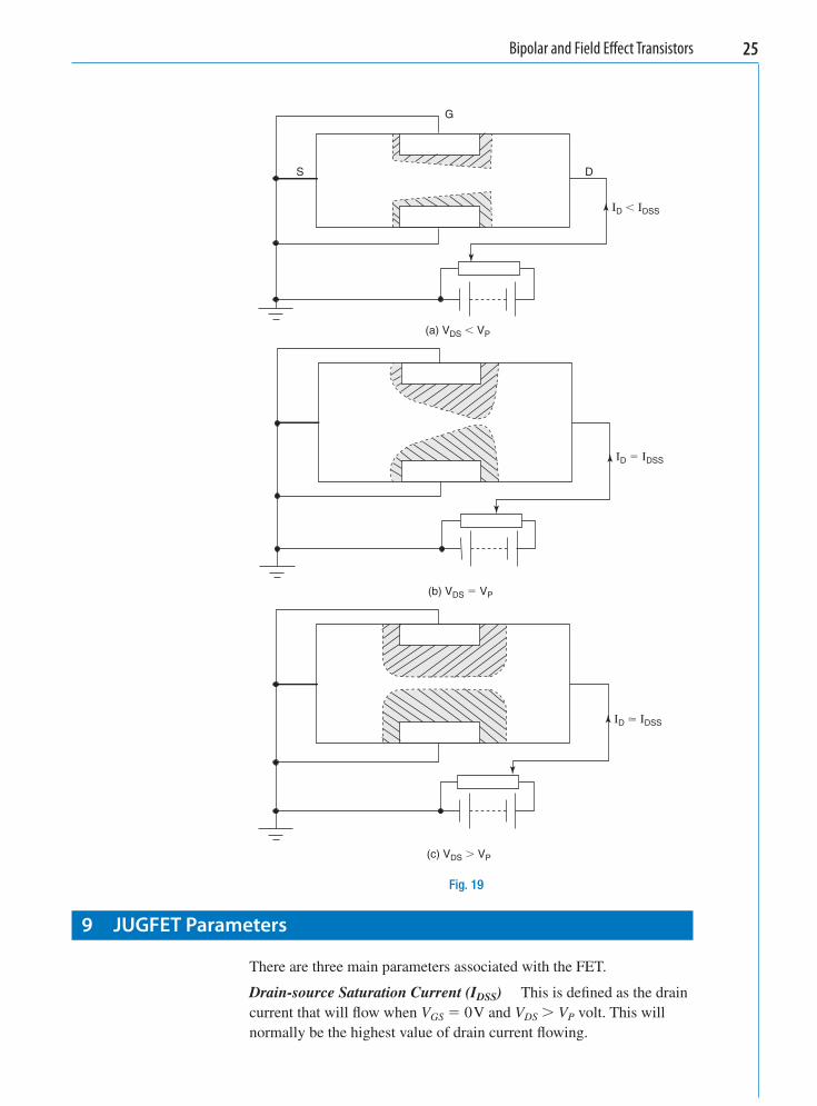
The reasons for the shape of the output characteristics are illustrated in Figs. 19(a) to (c) for the condition where V GS � 0.
From Fig. 19 it may be seen that the dimensions of the conducting channel for V DS � V p remain virtually constant, hence the current also stays sensibly constant. Although not shown in this series of diagrams, the increase of the negative potential to the gate electrode will also contribute to the narrowing of the conducting channel, and this is clearly demonstrated by the family of output characteristics. The application of a negative potential to the gate therefore reduces (or depletes) the drain current below I DSS , and the FET is said to be operating in depletion mode. This is the normal way in which the device is used. It is not normally operated with the gate potential greater than about 0.5 V since this will forward bias the p-n junction, which will then draw signifi cant current into the gate electrode.
WEBA-CHAP2.indd 24 5/2/2008 3:10:27 PM
Bipolar and Field Eff ect Transistors 25
(a) VDS � VP
S D
�D � �DSS
G
(b) VDS � VP
�D � �DSS
(c) VDS � VP
�D � �DSS
Fig. 19
9 JUGFET Parameters
There are three main parameters associated with the FET.
Drain-source Saturation Current (I DSS ) This is defi ned as the drain current that will fl ow when V GS � 0 V and V DS � V P volt. This will normally be the highest value of drain current fl owing.
WEBA-CHAP2.indd 25 5/2/2008 3:10:28 PM
26 Bipolar and Field Eff ect Transistors
Drain-source Resistance (r DS ) This parameter is defi ned as the ratio of drain-source voltage to drain-source current for a given value (often 0 V) of gate-source voltage. Thus
r
V
IVDS
DS
DSGS�
��
ohm, with constant
This parameter may be obtained from the output characteristics, and typical values would be in the low to mid kilohm range.
Mutual Conductance or Transconductance ( g m ) This parameter may be obtained from the transfer characteristic of Fig. 18(b), where it may be seen that the slope of the graph at any point is given by the value of drain current at that point divided by the corresponding value of gate-source voltage. Thus
g
I
VVm
D
GSDS�
��
siemen, with constant
Typical values for g m range from 0.05 mS to 10 mS. A value for g m may also be obtained from the output characteristics in a similar manner to that used to obtain h F for the BJT.
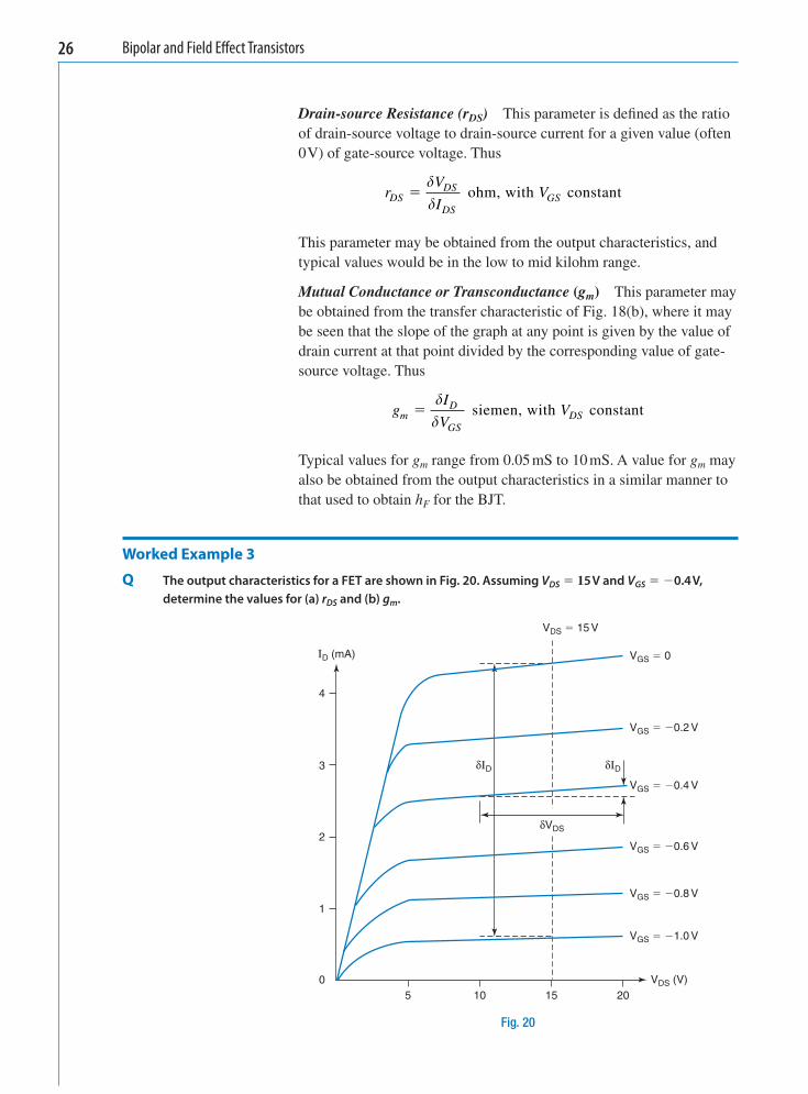
Worked Example 3
Q The output characteristics for a FET are shown in Fig. 20 . Assuming V DS � 15 V and V GS � � 0.4 V, determine the values for (a) r DS and (b) g m .
05 10 15 20
1
2
3
4
�D (mA)
VDS � 15 V
δ�D δ�D
δVDS
VDS (V)
VGS � 0
VGS � �0.2 V
VGS � �0.4 V
VGS � �0.6 V
VGS � �0.8 V
VGS � �1.0 V
Fig. 20
WEBA-CHAP2.indd 26 5/2/2008 3:10:28 PM

Bipolar and Field Eff ect Transistors 27
A
(a) With V GS � � 0.4 V and � V DS � (20 � 10) � 10 V the corresponding change in drain current, � I D � (2.7 � 2.55) mA � 0.15 mA
rV
r
DSDS
D
DS
� �
�
��
�
I ohm
k
1
1
00 5
66 7
.
. Ans
(b) For V DS � 15 V and � V GS � 0 � ( � 1) � 1 V the corresponding change in drain current, � I D � (4.4 � 0.6) mA � 3.8 mA
gV
g
mD
G S
m
� � �
�
���
I siemen
mS
3 8 0
3 8
3.
.
1
Ans
10 The Metal-Oxide-Semiconductor Transistor (MOSFET)
This device is an insulated gate FET (IGFET) as previously stated. It consists of a lightly doped p-type substrate into which are diffused two heavily doped n-type regions which form the source and drain. On the upper surface is deposited a very thin layer of silicon oxide which acts as an insulating layer. External electrical connections to the source and drain regions are via holes or windows left in the oxide layer. A cross-section of the transistor is shown in Fig. 21 .
S(�) G(�) D(�)metalconnections
oxide layer
n n
induced n-channel
p-substrate
Fig. 21
When a positive potential is applied to the gate terminal the resulting electric fi eld will attract electrons (from thermally generated electron-hole pairs) towards the top surface of the substrate, and repel holes away from it. As the gate potential is increased more electrons are attracted towards the upper surface until, at a voltage known as the threshold voltage, V T , a conducting or inversion channel of n-type semiconductor is induced between source and drain. For this reason this device is called an n-channel MOSFET. A typical value for V T is between 2 V and 4 V. When the gate potential is increased beyond V T even more electrons are attracted into the conducting channel. This will have the effect of increasing or enhancing the drain current, and
WEBA-CHAP2.indd 27 5/2/2008 3:10:29 PM

28
this mode of operation is known as enhancement mode. If an n-type substrate is used with p-type drain and source, and the polarities at the three electrodes are reversed, then a p-type channel is induced, and the device is called a p-channel MOSFET.
The circuit symbols for both types are shown in Fig. 22. Note that the channel between source and drain is shown as a broken line, because until V GS � V T the transistor will not conduct. In addition, although there is never any electrical connection made to the substrate, it is always shown on the circuit symbol, and the arrowhead indicates which type of channel is employed.
G(�) Substrate
D(�)
S(�)
(a) n-channel
G(�) Substrate
D(�)
S(�)
(b) p-channel
Fig. 22
Typical characteristics for an n-channel enhancement mode MOSFET are shown in Fig. 23 .
VGS � 8 V
VGS � 9 V
VGS � 7 V
VGS � 6 VVGS � 5 VVGS � 4 V
�D (mA)5
4
3
2
1
02 4 6 8 10
VDS (V)
(a) output characteristics
�D (mA)5
4
3
2
1
02
VT
4 6 8 10VDS (V)
VDS � 5 V
(b) transfer characteristics
Fig. 23
11 Depletion Mode MOSFET
The construction of this device is very similar to that for the enhancement mode device but with the exception that, during the manufacturing process, a conducting channel is diffused between source and drain. This is referred to as the initial channel, and the physical arrangement is illustrated in Fig. 24(a) .
Fig. 24(b) is used to describe the operation, as follows. Since the source and drain are joined by a conducting channel then drain current can fl ow even when V GS is zero. When the gate potential is made negative, the electric fi eld will attract holes from the substrate into
Bipolar and Field Eff ect Transistors
WEBA-CHAP2.indd 28 5/2/2008 3:10:29 PM

Bipolar and Field Eff ect Transistors 29
the n-channel, where recombinations will occur. Thus the number of free electrons in the n-channel is reduced or depleted, and the drain current will be reduced. It should be noted that if the gate is made positive then more electrons will be attracted into the channel and drain current will increase. Thus this device may be used in either depletion or enhancement mode. The circuit symbols for both n- and p-channel devices are shown in Fig. 25 . In these cases the conducting channel being a permanent feature, it is shown by a continuous line.
diffused channel
S(�)
n nn
(a) construction
G(�)D(�)
p
S(�)G(�)
D(�)
n nn
(b) operation
� � � � �
p
Fig. 24
G(�)
D(�)
S(�)
(a) n-channel
G(�)
D(�)
S(�)
(b) p-channel
Fig. 25
Typical output and transfer characteristics for the device are shown in Fig. 26 .
Typical values for the MOSFET parameters are:
Drain-source resistance, r D � 1 to 50 k � Gate input resistance, r G � 10 G � Mutual conductance, g m � 0.1 to 25 mS
106 8420
(a) output characteristics
1
2
3
4
5
�D (mA)
VGS � �3 VVGS � �2 V
VGS � �1 V
VGS � 0 V
VGS � �1 V
VGS � �2 V
VDS (V)
(b) transfer characteristics
�D (mA)
VGS (V)�2 20 4
depletion enhancement
VT
5
4
3
2
1
Fig. 26
WEBA-CHAP2.indd 29 5/2/2008 3:10:30 PM
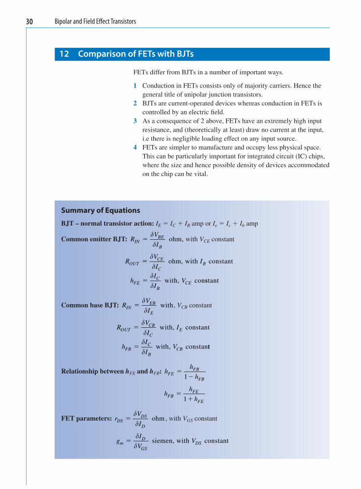
12 Comparison of FETs with BJTs
FETs differ from BJTs in a number of important ways.
1 Conduction in FETs consists only of majority carriers. Hence the general title of unipolar junction transistors.
2 BJTs are current-operated devices whereas conduction in FETs is controlled by an electric fi eld.
3 As a consequence of 2 above, FETs have an extremely high input resistance, and (theoretically at least) draw no current at the input, i.e there is negligible loading effect on any input source.
4 FETs are simpler to manufacture and occupy less physical space. This can be particularly important for integrated circuit (IC) chips, where the size and hence possible density of devices accommodated on the chip can be vital.
Summary of Equations
BJT – normal transistor action: I E � I C � I B amp or I e � I c � I b amp
Common emitter BJT: R
V
IINBE
B
���
ohm, with V CE constant
RV
II
hI
IV
OUTCE
CB
FEC
BCE
�
�
����
ohm, with constant
with, consstant
Common base BJT:
R
V
IINEB
E
���
with , V CB constant
RV
II
hI
IV
OUTCB
CE
FBC
BCB
�
�
����
with, constant
with, constantt
Relationship between h FE and h FB : h
h
hFEFB
FB
��1
h
h
hFBFE
FE
��1
FET parameters:
r
V
IDSDS
D
���
ohm , with V GS constant
g
I
VVm
D
GSDS�
��
siemen, with constant
30 Bipolar and Field Eff ect Transistors
WEBA-CHAP2.indd 30 5/2/2008 3:10:32 PM

Assignment Questions
1 A common emitter connected transistor has characteristics as shown in Fig. 27 . Using these graphs determine (a) transistor output resistance for a base current of 80 µ A, (b) transistor input resistance, and (c) transistor current gain for V CE � 6 V.
2 For the common base characteristics shown in Fig. 28 determine (a) transistor current gain, (b) output resistance, and (c) the
corresponding value of transistor current gain if the transistor was connected in common emitter confi guration.
3 A FET has characteristics as given in Table 2 below. Plot these characteristics and hence determine the parameters (a) drain-source resistance, and (b) mutual conductance for V GS � 12 V.
Bipolar and Field Eff ect Transistors 31
140
120
100
80
60
40
20
00.2 0.4 0.6 0.8
VBE (V)(b)(a)
�B (µA) Inputcharacteristics
35
30
25
20
15
10
5
0 0 2 4 6
VCE (V)
8 10 12
�B � 140 µA
�B � 120 µA
�B � 100 µA
�B � 80 µA
�B � 60 µA
�B � 40 µA
�B � 20 µA
� C (m
A)
Outputcharacteristics
Fig. 27
WEBA-CHAP2.indd 31 5/2/2008 3:10:32 PM

02 4 6 8 10
1
2
3
4
�C (mA)
VCB (V)
�E � 1 mA
�E � 2 mA
�E � 3 mA
�E � 4 mA
Fig. 28
Table 2
V DS I DS (mA)
( V ) V GS � � 2.5 V V GS � � 2.0 V V GS � � 1.5 V V GS � � 1.0 V V GS � � 0.5 V
4 0.6 1.4 2.0 3.0 4.0
16 1.0 3.1 3.6 4.8 6.4
24 1.4 3.7 4.6 6.0 8.0
Assignment Questions
32 Bipolar and Field Eff ect Transistors
WEBA-CHAP2.indd 32 5/2/2008 3:10:32 PM

Suggested Practical Assignments
For the following assignments it is left to the student (under the guidance of the teacher) to select appropriate apparatus. The circuit diagrams and method to follow are to be found in the relevant sections (3, 4 and 9). For each assignment all results should be tabulated and the corresponding graphs plotted.
Assignment 1 To obtain the output and input characteristics for a BJT when connected (a) in common base, and (b) in common emitter confi guration. From the plotted graphs determine the transistor parameters in each confi guration, and compare the relationship between transistor gain of the two confi gurations with the theoretical value.
Assignment 2 To obtain the output and transfer characteristics for a FET, and from the plotted graphs determine the transistor parameters.
Bipolar and Field Eff ect Transistors 33
WEBA-CHAP2.indd 33 5/2/2008 3:10:33 PM

Answers to Assignment Questions
1 (a) 1.58 k � (b) 360 � (c) 212
2 (a) 0.997 (b) 200 k � (c) 332
3 (a) 7.7 k � (b) 2. 7 ms
34 Bipolar and Field Eff ect Transistors
WEBA-CHAP2.indd 34 5/2/2008 3:10:33 PM