Embed Size (px)
Citation preview
AVAILABLE
Functional Diagrams
Pin Configurations appear at end of data sheet.Functional Diagrams continued at end of data sheet.UCSP is a trademark of Maxim Integrated Products, Inc.
For pricing, delivery, and ordering information, please contact Maxim Direct at 1-888-629-4642, or visit Maxim’s website at www.maximintegrated.com.
General DescriptionThe DS24B33 is a 4096-bit, 1-Wire® EEPROM orga-nized as 16 memory pages of 256 bits each. Data iswritten to a 32-byte scratchpad, verified, and thencopied to the EEPROM memory. The DS24B33 commu-nicates over a single-conductor 1-Wire bus. The com-munication follows the standard 1-Wire protocol. Eachdevice has its own unalterable and unique 64-bit regis-tration number that is factory programmed into the chip.The registration number is used to address the devicein a multidrop 1-Wire net environment. The DS24B33 issoftware compatible to the DS2433.
ApplicationsStorage of Calibration Constants
Board Identification
Storage of Product Revision Status
Features 4096 Bits of Nonvolatile EEPROM Partitioned Into
Sixteen 256-Bit Pages
Read and Write Access is Highly Backward-Compatible to the DS2433
256-Bit Scratchpad with Strict Read/WriteProtocols Ensures Integrity of Data Transfer
Unique, Factory-Programmed, 64-Bit RegistrationNumber Ensures Error-Free Device Selection andAbsolute Part Identity
Switchpoint Hysteresis to Optimize Performancein the Presence of Noise
Communicates to Host at 15.4kbps or 125kbpsUsing 1-Wire Protocol
Low-Cost Through-Hole and SMD Packages
Operating Range: +2.8V to +5.25V, -40°C to +85°C
IEC 1000-4-2 Level 4 ESD Protection (±8kVContact, ±15kV Air, Typical) for IO Pin
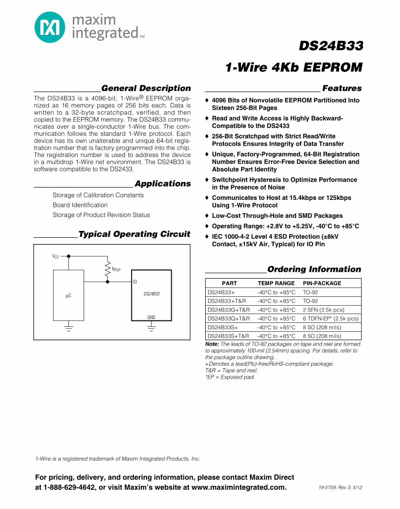
1-Wire 4Kb EEPROM
Ordering InformationIO
RPUP
VCC
µC
GND
DS24B33
Typical Operating Circuit
Note: The leads of TO-92 packages on tape and reel are formedto approximately 100-mil (2.54mm) spacing. For details, refer tothe package outline drawing.+Denotes a lead(Pb)-free/RoHS-compliant package.T&R = Tape and reel.*EP = Exposed pad.
PART TEMP RANGE PIN-PACKAGE
DS24B33+ -40°C to +85°C TO-92
DS24B33+T&R -40°C to +85°C TO-92
DS24B33G+T&R -40°C to +85°C 2 SFN (2.5k pcs)
DS24B33Q+T&R -40°C to +85°C 6 TDFN-EP* (2.5k pcs)
DS24B33S+ -40°C to +85°C 8 SO (208 mils)
DS24B33S+T&R -40°C to +85°C 8 SO (208 mils)
1-Wire is a registered trademark of Maxim Integrated Products, Inc.
19-5759; Rev 3; 5/12
DS24B33
1-Wire 4Kb EEPROMABSOLUTE MAXIMUM RATINGS
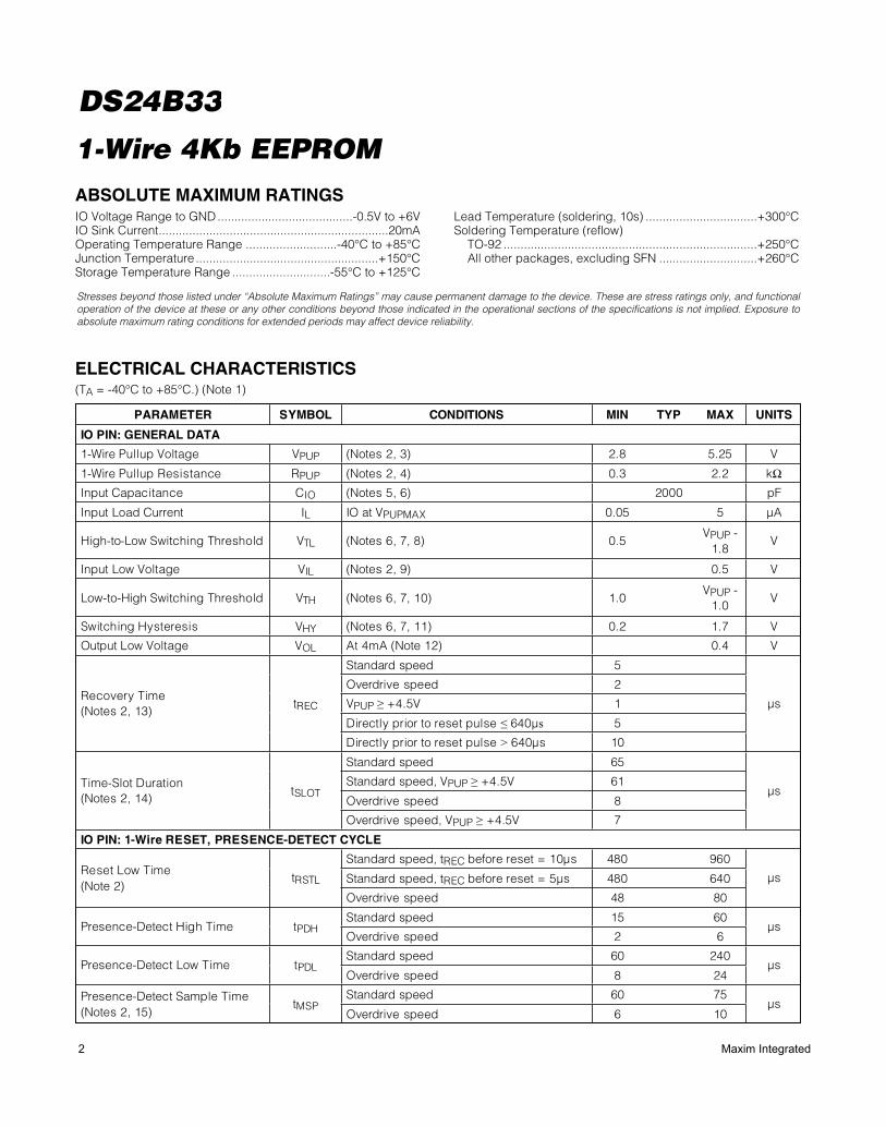
ELECTRICAL CHARACTERISTICS(TA = -40°C to +85°C.) (Note 1)
Stresses beyond those listed under “Absolute Maximum Ratings” may cause permanent damage to the device. These are stress ratings only, and functionaloperation of the device at these or any other conditions beyond those indicated in the operational sections of the specifications is not implied. Exposure toabsolute maximum rating conditions for extended periods may affect device reliability.
IO Voltage Range to GND........................................-0.5V to +6VIO Sink Current....................................................................20mAOperating Temperature Range ...........................-40°C to +85°CJunction Temperature ......................................................+150°CStorage Temperature Range .............................-55°C to +125°C
Lead Temperature (soldering, 10s) .................................+300°CSoldering Temperature (reflow)
TO-92 ...........................................................................+250°CAll other packages, excluding SFN .............................+260°C
PARAMETER SYMBOL CONDITIONS MIN TYP MAX UNITS
IO PIN: GENERAL DATA
1-Wire Pullup Voltage VPUP (Notes 2, 3) 2.8 5.25 V
1-Wire Pullup Resistance RPUP (Notes 2, 4) 0.3 2.2 k
Input Capacitance CIO (Notes 5, 6) 2000 pF
Input Load Current IL IO at VPUPMAX 0.05 5 µA
High-to-Low Switching Threshold VTL (Notes 6, 7, 8) 0.5 VPUP -
1.8 V
Input Low Voltage VIL (Notes 2, 9) 0.5 V
Low-to-High Switching Threshold VTH (Notes 6, 7, 10) 1.0 VPUP -
1.0 V
Switching Hysteresis VHY (Notes 6, 7, 11) 0.2 1.7 V
Output Low Voltage VOL At 4mA (Note 12) 0.4 V
Standard speed 5
Overdrive speed 2
VPUP +4.5V 1
Directly prior to reset pulse 640µs 5
Recovery Time (Notes 2, 13)
tREC
Directly prior to reset pulse > 640µs 10
µs
Standard speed 65
Standard speed, VPUP +4.5V 61
Overdrive speed 8 Time-Slot Duration (Notes 2, 14)
tSLOT
Overdrive speed, VPUP +4.5V 7
µs
IO PIN: 1-Wire RESET, PRESENCE-DETECT CYCLE
Standard speed, tREC before reset = 10µs 480 960
Standard speed, tREC before reset = 5µs 480 640 Reset Low Time (Note 2)
tRSTL
Overdrive speed 48 80
µs
Standard speed 15 60 Presence-Detect High Time tPDH
Overdrive speed 2 6 µs
Standard speed 60 240 Presence-Detect Low Time tPDL
Overdrive speed 8 24 µs
Standard speed 60 75 Presence-Detect Sample Time (Notes 2, 15)
tMSP Overdrive speed 6 10
µs
2 Maxim Integrated
DS24B33
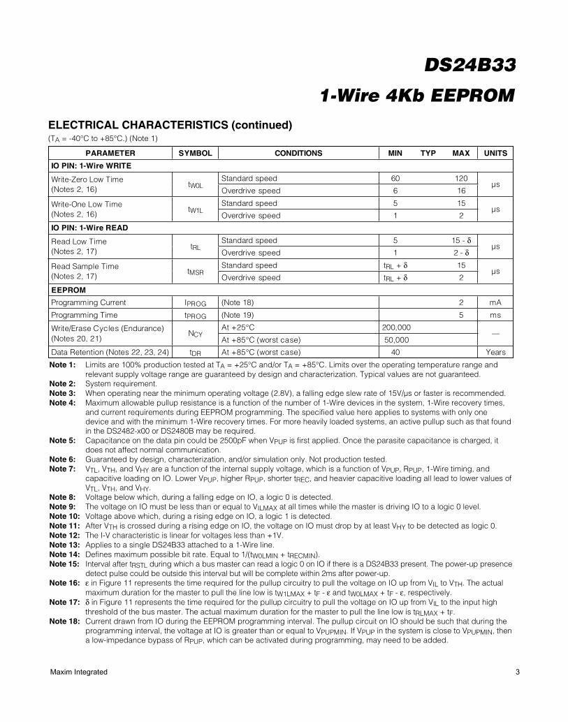
1-Wire 4Kb EEPROMELECTRICAL CHARACTERISTICS (continued)(TA = -40°C to +85°C.) (Note 1)
PARAMETER SYMBOL CONDITIONS MIN TYP MAX UNITS
IO PIN: 1-Wire WRITE
Standard speed 60 120 Write-Zero Low Time (Notes 2, 16)
tW0L Overdrive speed 6 16
µs
Standard speed 5 15 Write-One Low Time (Notes 2, 16)
tW1L Overdrive speed 1 2
µs
IO PIN: 1-Wire READ
Standard speed 5 15 - Read Low Time (Notes 2, 17)
tRL Overdrive speed 1 2 -
µs
Standard speed tRL + 15 Read Sample Time (Notes 2, 17)
tMSR Overdrive speed tRL + 2
µs
EEPROM
Programming Current IPROG (Note 18) 2 mA
Programming Time tPROG (Note 19) 5 ms
At +25°C 200,000 Write/Erase Cycles (Endurance) (Notes 20, 21)
NCYAt +85°C (worst case) 50,000
—
Data Retention (Notes 22, 23, 24) tDR At +85°C (worst case) 40 Years
Note 1: Limits are 100% production tested at TA = +25°C and/or TA = +85°C. Limits over the operating temperature range and relevant supply voltage range are guaranteed by design and characterization. Typical values are not guaranteed.
Note 2: System requirement.Note 3: When operating near the minimum operating voltage (2.8V), a falling edge slew rate of 15V/µs or faster is recommended.Note 4: Maximum allowable pullup resistance is a function of the number of 1-Wire devices in the system, 1-Wire recovery times,
and current requirements during EEPROM programming. The specified value here applies to systems with only onedevice and with the minimum 1-Wire recovery times. For more heavily loaded systems, an active pullup such as that foundin the DS2482-x00 or DS2480B may be required.
Note 5: Capacitance on the data pin could be 2500pF when VPUP is first applied. Once the parasite capacitance is charged, itdoes not affect normal communication.
Note 6: Guaranteed by design, characterization, and/or simulation only. Not production tested.Note 7: VTL, VTH, and VHY are a function of the internal supply voltage, which is a function of VPUP, RPUP, 1-Wire timing, and
capacitive loading on IO. Lower VPUP, higher RPUP, shorter tREC, and heavier capacitive loading all lead to lower values ofVTL, VTH, and VHY.
Note 8: Voltage below which, during a falling edge on IO, a logic 0 is detected.Note 9: The voltage on IO must be less than or equal to VILMAX at all times while the master is driving IO to a logic 0 level.Note 10: Voltage above which, during a rising edge on IO, a logic 1 is detected.Note 11: After VTH is crossed during a rising edge on IO, the voltage on IO must drop by at least VHY to be detected as logic 0.Note 12: The I-V characteristic is linear for voltages less than +1V.Note 13: Applies to a single DS24B33 attached to a 1-Wire line.Note 14: Defines maximum possible bit rate. Equal to 1/(tW0LMIN + tRECMIN).Note 15: Interval after tRSTL during which a bus master can read a logic 0 on IO if there is a DS24B33 present. The power-up presence
detect pulse could be outside this interval but will be complete within 2ms after power-up.Note 16: ε in Figure 11 represents the time required for the pullup circuitry to pull the voltage on IO up from VIL to VTH. The actual
maximum duration for the master to pull the line low is tW1LMAX + tF - ε and tW0LMAX + tF - ε, respectively.Note 17: δ in Figure 11 represents the time required for the pullup circuitry to pull the voltage on IO up from VIL to the input high
threshold of the bus master. The actual maximum duration for the master to pull the line low is tRLMAX + tF.Note 18: Current drawn from IO during the EEPROM programming interval. The pullup circuit on IO should be such that during the
programming interval, the voltage at IO is greater than or equal to VPUPMIN. If VPUP in the system is close to VPUPMIN, thena low-impedance bypass of RPUP, which can be activated during programming, may need to be added.
Maxim Integrated 3
DS24B33
2
3
1
2
3
1
3
2
1
N.C.
IO
GND
TO-92 FRONT VIEW (T&R VERSION)
FRONT VIEWSIDE VIEW
1
2
3
4
N.C.
N.C.
IO
GND
N.C.
N.C.
N.C.
N.C.
NOTE: THE SFN PACKAGE IS QUALIFIED FOR ELECTRO-MECHANICAL CONTACTAPPLICATIONS ONLY, NOT FOR SOLDERING. FOR MORE INFORMATION, REFER TOAPPLICATION NOTE 4132: ATTACHMENT METHODS FOR ELECTRO-MECHANICALSFN PACKAGE.
8
7
6
5
DS24B33
SO(208 mils)
TOP VIEW
+
SFN(6mm × 6mm × 0.9mm)
BOTTOM VIEW
1 2
IO GNDDS24B33
DS24B33
1 6N.C. N.C.
2 5IO N.C.
3 4GND N.C.
TDFN(3mm × 3mm)
TOP VIEW
24
B3
3ym
rrF
+
*EP
*EXPOSED PAD
ELECTRICAL CHARACTERISTICS (continued)(TA = -40°C to +85°C.) (Note 1)
Note 19: The tPROG interval begins after the trailing rising edge on IO for the last time slot of the E/S byte for a valid copy scratch-pad sequence. The interval ends once the device’s self-timed EEPROM programming cycle is complete and the currentdrawn by the device has returned from IPROG to IL.
Note 20: Write-cycle endurance is degraded as TA increases.Note 21: Not 100% production tested; guaranteed by reliability monitor sampling.Note 22: Data retention is degraded as TA increases.Note 23: Guaranteed by 100% production test at elevated temperature for a shorter time; equivalence of this production test to data
sheet limit at operating temperature range is established by reliability testing.Note 24: EEPROM writes can become nonfunctional after the data-retention time is exceeded. Long-time storage at elevated tem-
peratures is not recommended; the device can lose its write capability after 10 years at +125°C or 40 years at +85°C.
1-Wire 4Kb EEPROM
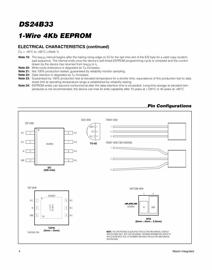
Pin Configurations
4 Maxim Integrated
DS24B33
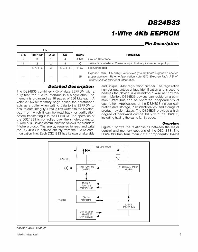
Detailed DescriptionThe DS24B33 combines 4Kb of data EEPROM with afully featured 1-Wire interface in a single chip. Thememory is organized as 16 pages of 256 bits each. Avolatile 256-bit memory page called the scratchpadacts as a buffer when writing data to the EEPROM toensure data integrity. Data is first written to the scratch-pad, from which it can be read back for verificationbefore transferring it to the EEPROM. The operation ofthe DS24B33 is controlled over the single-conductor1-Wire bus. Device communication follows the standard1-Wire protocol. The energy required to read and writethe DS24B33 is derived entirely from the 1-Wire com-munication line. Each DS24B33 has its own unalterable
and unique 64-bit registration number. The registrationnumber guarantees unique identification and is used toaddress the device in a multidrop 1-Wire net environ-ment. Multiple DS24B33 devices can reside on a com-mon 1-Wire bus and be operated independently ofeach other. Applications of the DS24B33 include cali-bration data storage, PCB identification, and storage ofproduct revision status. The DS24B33 provides a highdegree of backward compatibility with the DS2433,including having the same family code.
OverviewFigure 1 shows the relationships between the majorcontrol and memory sections of the DS24B33. TheDS24B33 has four main data components: 64-bit
Pin DescriptionPIN
SFN TDFN-EP TO-92 SO NAME FUNCTION
2 3 1 4 GND Ground Reference
1 2 2 3 IO 1-Wire Bus Interface. Open-drain pin that requires external pullup
— 1, 4, 5, 6 3 1, 2, 5–8 N.C. Not Connected
— — — — EP Exposed Pad (TDFN only). Solder evenly to the board’s ground plane for proper operation. Refer to Application Note 3273: Exposed Pads: A Brief Introduction for additional information.
1-Wire 4Kb EEPROM
DS24B33
1-Wire FUNCTIONCONTROL
1-Wire NET
PARASITE POWER
CRC-16GENERATOR
64-BIT REGISTRATIONNUMBER
32-BYTESCRATCHPAD
DATA MEMORY16 PAGES OF
32 BYTES EACH
MEMORYFUNCTION
CONTROL UNIT
Figure 1. Block Diagram
Maxim Integrated 5
DS24B33
1-Wire 4Kb EEPROM
AVAILABLE COMMANDS: DATA FIELD AFFECTED:
READ ROMMATCH ROMSEARCH ROMSKIP ROMRESUMEOVERDRIVE-SKIP ROMOVERDRIVE-MATCH ROM
64-BIT REG. #, RC-FLAG64-BIT REG. #, RC-FLAG64-BIT REG. #, RC-FLAGRC-FLAGRC-FLAGRC-FLAG, OD-FLAG64-BIT REG. #, RC-FLAG, OD-FLAG
1-Wire ROMFUNCTION COMMANDS
WRITE SCRATCHPADREAD SCRATCHPADCOPY SCRATCHPADREAD MEMORY
32-BYTE SCRATCHPAD, FLAGS32-BYTE SCRATCHPADDATA MEMORYDATA MEMORY
DS24B33-SPECIFICMEMORY FUNCTION COMMANDS
COMMAND LEVEL:
DS24B33
Figure 2. Hierarchical Structure for 1-Wire Protocol
MSB
8-BITCRC CODE 48-BIT SERIAL NUMBER
MSB MSBLSB
LSB
LSB
8-BIT FAMILY CODE(23h)
MSBLSB
Figure 3. 64-Bit Registration Number
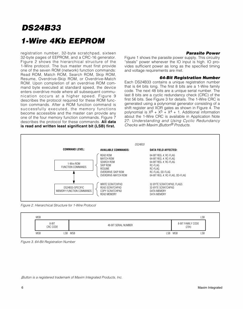
registration number, 32-byte scratchpad, sixteen32-byte pages of EEPROM, and a CRC-16 generator.Figure 2 shows the hierarchical structure of the1-Wire protocol. The bus master must first provideone of the seven ROM (network) function commands:Read ROM, Match ROM, Search ROM, Skip ROM,Resume, Overdrive-Skip ROM, or Overdrive-MatchROM. Upon completion of an overdrive ROM com-mand byte executed at standard speed, the deviceenters overdrive mode where all subsequent commu-nicat ion occurs at a h igher speed. F igure 9describes the protocol required for these ROM func-tion commands. After a ROM function command issuccessfu l ly executed, the memory funct ionsbecome accessible and the master can provide anyone of the four memory function commands. Figure 7describes the protocol for these commands. All datais read and written least significant bit (LSB) first.
Parasite PowerFigure 1 shows the parasite power supply. This circuitry“steals” power whenever the IO input is high. IO pro-vides sufficient power as long as the specified timingand voltage requirements are met.
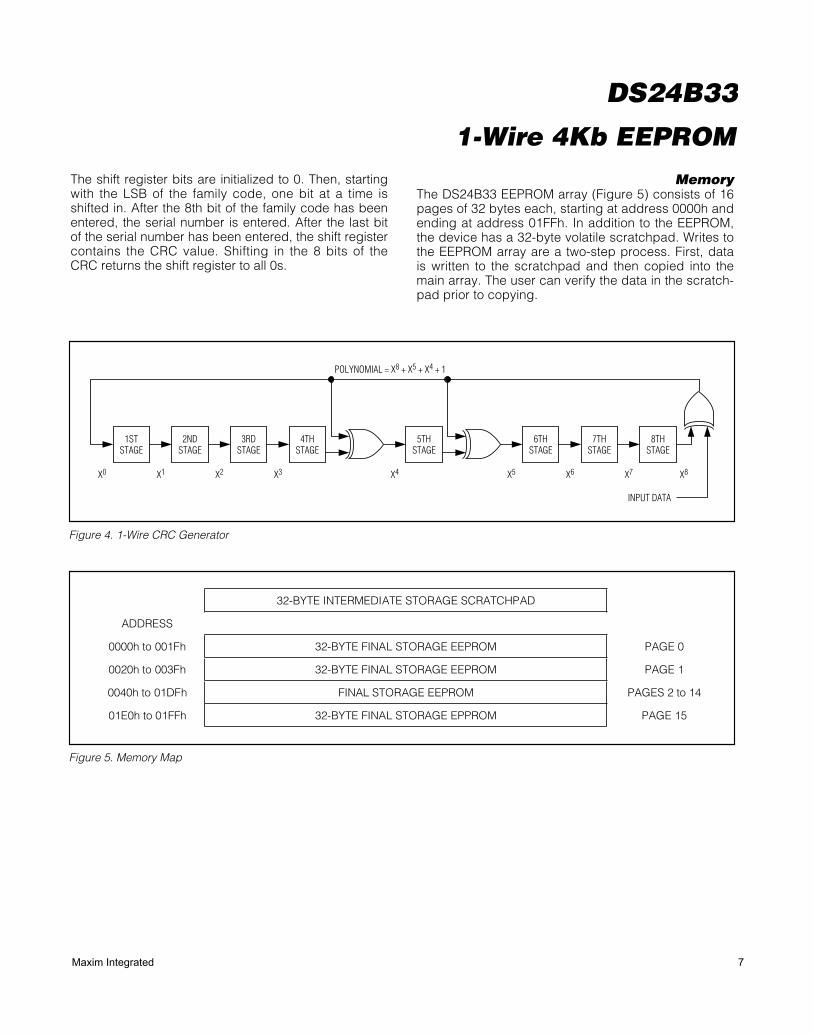
64-Bit Registration NumberEach DS24B33 contains a unique registration numberthat is 64 bits long. The first 8 bits are a 1-Wire familycode. The next 48 bits are a unique serial number. Thelast 8 bits are a cyclic redundancy check (CRC) of thefirst 56 bits. See Figure 3 for details. The 1-Wire CRC isgenerated using a polynomial generator consisting of ashift register and XOR gates as shown in Figure 4. Thepolynomial is X8 + X5 + X4 + 1. Additional informationabout the 1-Wire CRC is available in Application Note27: Understanding and Using Cyclic RedundancyChecks with Maxim iButton® Products.
iButton is a registered trademark of Maxim Integrated Products, Inc.
6 Maxim Integrated
DS24B33
1-Wire 4Kb EEPROM
1STSTAGE
2NDSTAGE
3RDSTAGE
4THSTAGE
7THSTAGE
8THSTAGE
6THSTAGE
5THSTAGE
X0 X1 X2 X3 X4
POLYNOMIAL = X8 + X5 + X4 + 1
INPUT DATA
X5 X6 X7 X8
Figure 4. 1-Wire CRC Generator
32-BYTE INTERMEDIATE STORAGE SCRATCHPAD
ADDRESS
0000h to 001Fh 32-BYTE FINAL STORAGE EEPROM PAGE 0
0020h to 003Fh 32-BYTE FINAL STORAGE EEPROM PAGE 1
0040h to 01DFh FINAL STORAGE EEPROM PAGES 2 to 14
01E0h to 01FFh 32-BYTE FINAL STORAGE EPPROM PAGE 15
Figure 5. Memory Map
The shift register bits are initialized to 0. Then, startingwith the LSB of the family code, one bit at a time isshifted in. After the 8th bit of the family code has beenentered, the serial number is entered. After the last bitof the serial number has been entered, the shift registercontains the CRC value. Shifting in the 8 bits of theCRC returns the shift register to all 0s.
MemoryThe DS24B33 EEPROM array (Figure 5) consists of 16pages of 32 bytes each, starting at address 0000h andending at address 01FFh. In addition to the EEPROM,the device has a 32-byte volatile scratchpad. Writes tothe EEPROM array are a two-step process. First, datais written to the scratchpad and then copied into themain array. The user can verify the data in the scratch-pad prior to copying.
Maxim Integrated 7
DS24B33
1-Wire 4Kb EEPROMMemory Access
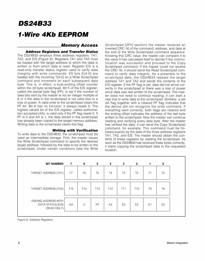
Address Registers and Transfer StatusThe DS24B33 employs three address registers: TA1,TA2, and E/S (Figure 6). Registers TA1 and TA2 mustbe loaded with the target address to which the data iswritten or from which data is read. Register E/S is aread-only transfer status register used to verify dataintegrity with write commands. ES bits E[4:0] areloaded with the incoming T[4:0] on a Write Scratchpadcommand and increment on each subsequent databyte. This is, in effect, a byte-ending offset counterwithin the 32-byte scratchpad. Bit 5 of the E/S register,called the partial byte flag (PF), is set if the number ofdata bits sent by the master is not an integer multiple of8 or if the data in the scratchpad is not valid due to aloss of power. A valid write to the scratchpad clears thePF bit. Bit 6 has no function; it always reads 0. Thehighest valued bit of the E/S register, called authoriza-tion accepted (AA), is valid only if the PF flag reads 0. IfPF is 0 and AA is 1, the data stored in the scratchpadhas already been copied to the target memory address.Writing data to the scratchpad clears this flag.
Writing with VerificationTo write data to the DS24B33, the scratchpad must beused as intermediate storage. First, the master issuesthe Write Scratchpad command to specify the desiredtarget address, followed by the data to be written to thescratchpad. Under certain conditions (see the Write
Scratchpad [0Fh] section) the master receives aninverted CRC-16 of the command, address, and data atthe end of the Write Scratchpad command sequence.Knowing this CRC value, the master can compare it tothe value it has calculated itself to decide if the commu-nication was successful and proceed to the CopyScratchpad command. If the master could not receivethe CRC-16, it should send the Read Scratchpad com-mand to verify data integrity. As a preamble to thescratchpad data, the DS24B33 repeats the targetaddress TA1 and TA2 and sends the contents of theE/S register. If the PF flag is set, data did not arrive cor-rectly in the scratchpad or there was a loss of powersince data was last written to the scratchpad. The mas-ter does not need to continue reading; it can start anew trial to write data to the scratchpad. Similarly, a setAA flag together with a cleared PF flag indicates thatthe device did not recognize the write command. Ifeverything went correctly, both flags are cleared andthe ending offset indicates the address of the last bytewritten to the scratchpad. Now the master can continuereading and verifying every data byte. After the masterhas verified the data, it can send the Copy Scratchpadcommand, for example. This command must be fol-lowed exactly by the data of the three address registersTA1, TA2, and E/S. The master should obtain the con-tents of these registers by reading the scratchpad. Assoon as the DS24B33 has received these bytes correctly,it starts copying the scratchpad data to the requestedlocation.
BIT NUMBER 7 6 5 4 3 2 1 0
TARGET ADDRESS (TA1) T7 T6 T5 T4 T3 T2 T1 T0
TARGET ADDRESS (TA2) T15 T14 T13 T12 T11 T10 T9 T8
ENDING ADDRESS WITH DATA STATUS (E/S)
(READ ONLY) AA 0 PF E4 E3 E2 E1 E0
Figure 6. Address Registers
8 Maxim Integrated
DS24B33
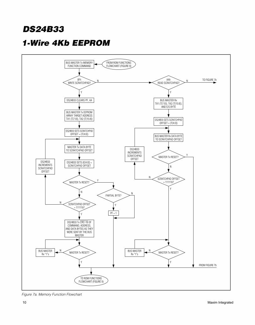
1-Wire 4Kb EEPROMMemory Function Commands
The Memory Function Flowchart (Figure 7) describesthe protocols necessary for accessing the memory ofthe DS24B33. The target address registers TA1 andTA2 are used for both read and write. The communica-tion between the master and the DS24B33 takes placeeither at standard speed (default, OD = 0) or at over-drive speed (OD = 1). If not explicitly set into the over-drive mode, the DS24B33 assumes standard speed.
Write Scratchpad [0Fh]The Write Scratchpad command applies to the datamemory. After issuing the Write Scratchpad command,the master must first provide the 2-byte target address,followed by the data to be written to the scratchpad.The data is written to the scratchpad starting at the byteoffset of T[4:0]. The ES bits E[4:0] are loaded with thestarting byte offset and increment with each subse-quent byte. Effectively, E[4:0] is the byte offset of thelast full byte written to the scratchpad. Only full bytesare accepted. If the last byte is incomplete, its contentis ignored and PF is set.
When executing the Write Scratchpad command, theCRC generator inside the DS24B33 (Figure 13) calcu-lates a 16-bit CRC of the entire data stream, starting atthe command code and ending at the last data byte assent by the master. This CRC is generated using theCRC-16 polynomial (X16 + X15 + X2 + 1) by first clear-ing the CRC generator and then shifting in the com-mand code (0Fh) of the Write Scratchpad command,the target addresses TA1 and TA2 as supplied by themaster, and all the data bytes. The master can end theWrite Scratchpad command at any time. However, if theend of the scratchpad is reached (E[4:0] = 11111b),the master can send 16 read time slots to receive theCRC generated by the DS24B33.
The DS24B33’s memory address range is 0000h to01FFh. If the bus master sends a target address higherthan this, the DS24B33’s internal circuitry sets the 7most significant address bits to zero as they are shiftedinto the internal address register. The Read Scratchpadcommand reveals the modified target address. Themaster identifies such address modifications by com-paring the target address read back to the targetaddress transmitted. If the master does not read thescratchpad, a subsequent Copy Scratchpad commanddoes not work because the most significant bits of thetarget address the master sends do not match thevalue that the DS24B33 expects.
Read Scratchpad [AAh]The Read Scratchpad command allows for verifying thetarget address and the integrity of the scratchpad data.After issuing the command code, the master beginsreading. The first 2 bytes are the target address. Thenext byte is the ending offset/data status byte (E/S) fol-lowed by the scratchpad data beginning at the byte off-set (T[4:0]). The master should read through the end ofthe scratchpad. If the master continues reading beyondthe end of the scratchpad, all data are logic 1s.
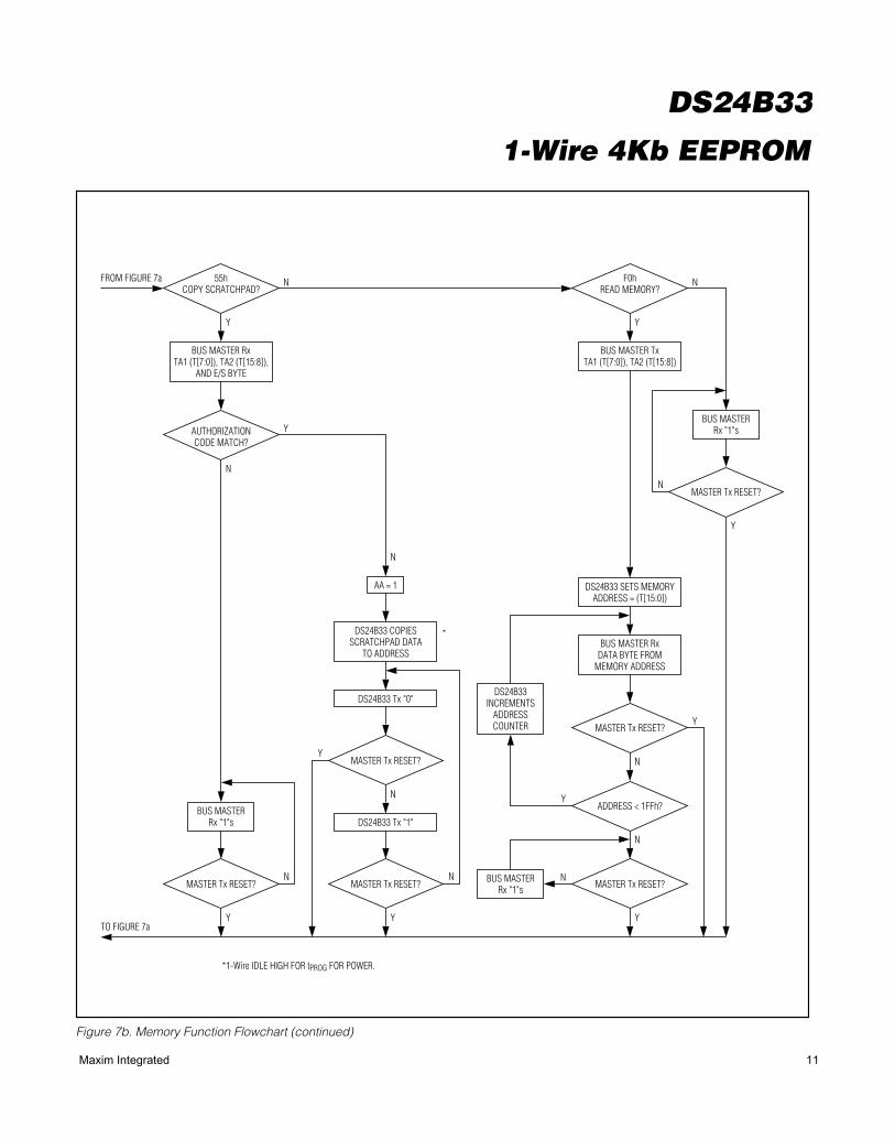
Copy Scratchpad [55h]The Copy Scratchpad command is used to copy datafrom the scratchpad to the data memory. After issuingthe Copy Scratchpad command, the master must pro-vide a 3-byte authorization pattern, which should havebeen obtained by an immediately preceding ReadScratchpad command. This 3-byte pattern must exactlymatch the data contained in the three address registers(TA1, TA2, E/S, in that order). If the pattern matchesand the target address is valid, the AA flag is set andthe copy begins. The data to be copied is determinedby the three address registers. The scratchpad datafrom the beginning offset through the ending offset iscopied to memory, starting at the target address.Anywhere from 1 to 32 bytes can be copied with thiscommand. The duration of the device’s internal datatransfer is tPROG, during which the voltage on the1-Wire bus must not fall below VPUPMIN. A pattern ofalternating 0s and 1s are transmitted after the data hasbeen copied until the master issues a reset pulse.
Note: Because of the memory architecture of theDS24B33, if a Copy Scratchpad command is interruptedduring the write cycle, two consecutive CopyScratchpad commands of the same data to the samelocation may be necessary to recover. To verify the suc-cess of the Copy Scratchpad command, always look forthe alternating 0-to-1 pattern at the end of the CopyScratchpad command flow and also read back the EEP-ROM page that was to be updated. If the alternatingpattern appeared and the EEPROM page data showsthe intended new data, the write access was successful.No further action is required. In all other cases (alternat-ing 0-to-1 pattern is not seen or nonmatching EEPROMpage data), repeat the Write Scratchpad, CopyScratchpad sequence until successful.
Maxim Integrated 9
DS24B33
1-Wire 4Kb EEPROM
BUS MASTER Tx MEMORYFUNCTION COMMAND
DS24B33 CLEARS PF, AA
MASTER Tx DATA BYTETO SCRATCHPAD OFFSET
DS24B33 SETS SCRATCHPADOFFSET = (T[4:0])
DS24B33 SETS SCRATCHPADOFFSET = (T[4:0])
BUS MASTERRx "1"s
DS24B33INCREMENTSSCRATCHPAD
OFFSET
PF = 1
BUS MASTER Tx EEPROMARRAY TARGET ADDRESSTA1 (T[7:0]), TA2 (T[15:8])
BUS MASTER RxTA1 (T[7:0]), TA2 (T[15:8]),
AND E/S BYTE
0FhWRITE SCRATCHPAD?
N
Y
N
Y
N
Y
Y
N
N
MASTER Tx RESET?
PARTIAL BYTE?
SCRATCHPAD OFFSET= 11111b?
MASTER Tx RESET?
DS24B33 SETS (E[4:0]) =SCRATCHPAD OFFSET
DS24B33 Tx CRC-16 OFCOMMAND, ADDRESS,
AND DATA BYTES AS THEYWERE SENT BY THE BUS
MASTER
BUS MASTERRx "1"s
Y
NMASTER Tx RESET?
Y
N
MASTER Tx RESET?
Y
SCRATCHPAD OFFSET= 11111b?
Y
FROM ROM FUNCTIONSFLOWCHART (FIGURE 9)
TO ROM FUNCTIONSFLOWCHART (FIGURE 9)
AAhREAD SCRATCHPAD?
N
Y
N
BUS MASTER Rx DATA BYTETO SCRATCHPAD OFFSET
DS24B33INCREMENTSSCRATCHPAD
OFFSET
TO FIGURE 7b
FROM FIGURE 7b
Figure 7a. Memory Function Flowchart
10 Maxim Integrated
DS24B33
1-Wire 4Kb EEPROM
DS24B33 Tx "1"
Y
N
AUTHORIZATIONCODE MATCH?
BUS MASTER RxTA1 (T[7:0]), TA2 (T[15:8]),
AND E/S BYTE
BUS MASTER TxTA1 (T[7:0]), TA2 (T[15:8])
55hCOPY SCRATCHPAD?
N
Y
F0hREAD MEMORY?
N
Y
DS24B33 COPIESSCRATCHPAD DATA
TO ADDRESS
*
*1-Wire IDLE HIGH FOR tPROG FOR POWER.
TO FIGURE 7a
FROM FIGURE 7a
BUS MASTERRx "1"s
MASTER Tx RESET?N
Y
MASTER Tx RESET?
MASTER Tx RESET?
N
DS24B33 Tx "0"
Y
N
N
Y
AA = 1
BUS MASTERRx "1"s
MASTER Tx RESET?N
Y
BUS MASTERRx "1"s
DS24B33 SETS MEMORYADDRESS = (T[15:0])
BUS MASTER RxDATA BYTE FROM
MEMORY ADDRESS
Y
N
N
MASTER Tx RESET?
ADDRESS < 1FFh?
N
Y
MASTER Tx RESET?
DS24B33INCREMENTS
ADDRESSCOUNTER
Y
Figure 7b. Memory Function Flowchart (continued)
Maxim Integrated 11
DS24B33
1-Wire 4Kb EEPROMRead Memory [F0h]
The Read Memory command is the general function toread from the DS24B33. After issuing the command,the master must provide a 2-byte target address, whichshould be in the range of 0000h to 01FFh. If the targetaddress is higher than 01FFh, the DS24B33 changesthe upper 7 address bits to 0. After the address istransmitted, the master reads data starting at the (modi-fied) target address and can continue until address01FFh. If the master continues reading, the result isFFh. The Read Memory command can be ended at anypoint by issuing a reset pulse. Note that the (modified)target address provided with the Read Memory com-mand overwrites the target address that was specifiedwith a previously issued Write Scratchpad command.The Read Memory command overwrites the scratchpadwith data from the target memory page. When readingthe last byte of a memory page, the scratchpad isloaded with data from the next memory page. Thiscould cause unexpected data to be loaded into thescratchpad.
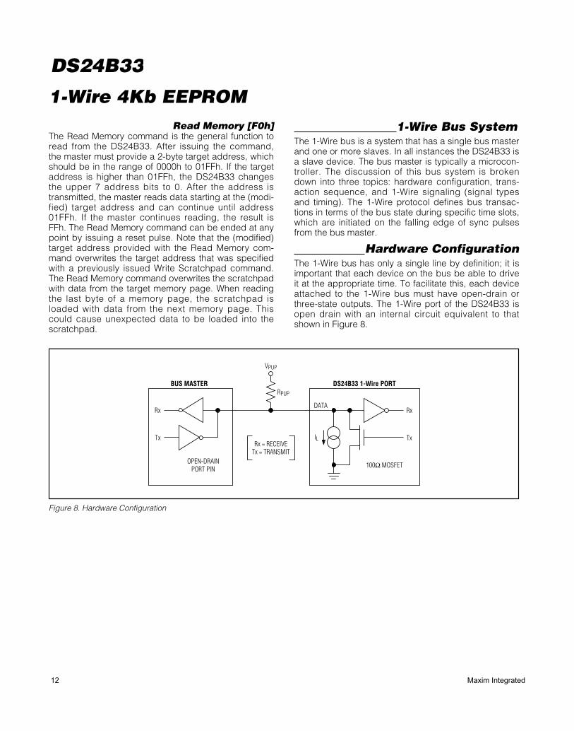
1-Wire Bus SystemThe 1-Wire bus is a system that has a single bus masterand one or more slaves. In all instances the DS24B33 isa slave device. The bus master is typically a microcon-troller. The discussion of this bus system is brokendown into three topics: hardware configuration, trans-action sequence, and 1-Wire signaling (signal typesand timing). The 1-Wire protocol defines bus transac-tions in terms of the bus state during specific time slots,which are initiated on the falling edge of sync pulsesfrom the bus master.
Hardware ConfigurationThe 1-Wire bus has only a single line by definition; it isimportant that each device on the bus be able to driveit at the appropriate time. To facilitate this, each deviceattached to the 1-Wire bus must have open-drain orthree-state outputs. The 1-Wire port of the DS24B33 isopen drain with an internal circuit equivalent to thatshown in Figure 8.
Rx
RPUP
IL
VPUP
BUS MASTER
OPEN-DRAINPORT PIN 100Ω MOSFET
Tx
Rx
Tx
DATA
DS24B33 1-Wire PORT
Rx = RECEIVETx = TRANSMIT
Figure 8. Hardware Configuration
12 Maxim Integrated
DS24B33
1-Wire 4Kb EEPROMA multidrop bus consists of a 1-Wire bus with multipleslaves attached. The DS24B33 supports both a stan-dard and overdrive communication speed of 15.4kbps(maximum) and 125kbps (maximum), respectively, overthe full pullup voltage range. For pullup voltages of+4.75V and higher, the DS24B33 also supports thelegacy communication speed of 16.3kbps and over-drive speed of 142kbps. The slightly reduced rates forthe DS24B33 are a result of additional recovery times,which in turn were driven by a 1-Wire physical interfaceenhancement to improve noise immunity. The value ofthe pullup resistor primarily depends on the networksize and load conditions. The DS24B33 requires apullup resistor of 2.2kΩ (maximum) at any speed.
The idle state for the 1-Wire bus is high. If for any rea-son a transaction must be suspended, the bus must beleft in the idle state if the transaction is to resume. If thisdoes not occur and the bus is left low for more than16µs (overdrive speed) or more than 120µs (standardspeed), one or more devices on the bus may be reset.
Transaction SequenceThe protocol for accessing the DS24B33 through the1-Wire port is as follows:
• Initialization
• ROM Function Commands
• Memory Function Commands
• Transaction/Data
InitializationAll transactions on the 1-Wire bus begin with an initial-ization sequence. The initialization sequence consistsof a reset pulse transmitted by the bus master followedby presence pulse(s) transmitted by the slave(s). Thepresence pulse lets the bus master know that theDS24B33 is on the bus and is ready to operate. Formore details, see the 1-Wire Signaling section.
1-Wire ROM Function CommandsOnce the bus master has detected a presence, it canissue one of the seven ROM function commands thatthe DS24B33 supports. All ROM function commands are8 bits long. See Figure 9 for a list of these commands.
Read ROM [33h]This command allows the bus master to read theDS24B33’s 8-bit family code, unique 48-bit serial num-ber, and 8-bit CRC. This command can only be used ifthere is a single slave on the bus. If more than oneslave is present on the bus, a data collision occurswhen all slaves try to transmit at the same time (opendrain produces a wired-AND result). The resultant familycode and 48-bit serial number results in a mismatch ofthe CRC.
Match ROM [55h]The Match ROM command, followed by a 64-bit ROMsequence, allows the bus master to address a specificDS24B33 on a multidrop bus. Only the DS24B33 thatexactly matches the 64-bit ROM sequence responds tothe memory function command that follows. All otherslaves wait for a reset pulse. This command can beused with a single device or multiple devices on thebus.
Search ROM [F0h]When a system is initially brought up, the bus mastermight not know the number of devices on the 1-Wirebus or their registration numbers. By taking advantageof the bus’s wired-AND property, the master can use aprocess of elimination to identify the registration num-bers of all slave devices. For each bit of the registrationnumber, starting with the LSB, the bus master issues atriplet of time slots. On the first slot, each slave deviceparticipating in the search outputs the true value of itsregistration number bit. On the second slot, each slavedevice participating in the search outputs the comple-mented value of its registration number bit. On the thirdslot, the master writes the true value of the bit to beselected. All slave devices that do not match the bitwritten by the master stop participating in the search. Ifboth of the read bits are zero, the master knows thatslave devices exist with both states of the bit. By choos-ing which state to write, the bus master branches in theROM code tree. After one complete pass, the bus mas-ter knows the registration number of a single device.Additional passes identify the registration numbers ofthe remaining devices. Refer to Application Note 187:1-Wire Search Algorithm for a detailed discussion andan example.
Maxim Integrated 13
DS24B33
1-Wire 4Kb EEPROMSkip ROM [CCh]
This command can save time in a single-drop bus sys-tem by allowing the bus master to access the memoryfunctions without providing the 64-bit ROM code. Ifmore than one slave is present on the bus and, forexample, a read command is issued following the SkipROM command, data collision occurs on the bus asmultiple slaves transmit simultaneously (open-drainpulldowns produce a wired-AND result).
Resume [A5h]To maximize the data throughput in a multidrop envi-ronment, the Resume command is available. This com-mand checks the status of the RC bit and, if it is set,directly transfers control to the memory functions, simi-lar to a Skip ROM command. The only way to set theRC bit is by successfully executing the Match ROM,Search ROM, or Overdrive-Match ROM command.Once the RC bit is set, the device can repeatedly beaccessed through the Resume command. Accessinganother device on the bus clears the RC bit, preventingtwo or more devices from simultaneously responding tothe Resume command.
Overdrive-Skip ROM [3Ch]On a single-drop bus, this command can save time byallowing the bus master to access the memory func-tions without providing the 64-bit ROM code. Unlike thenormal Skip ROM command, the Overdrive-Skip ROMcommand sets the DS24B33 in the overdrive mode (OD= 1). All communication following this command mustoccur at overdrive speed until a reset pulse of minimum480µs duration resets all devices on the bus to stan-dard speed (OD = 0).
When issued on a multidrop bus, this command sets alloverdrive-supporting devices into overdrive mode. Tosubsequently address a specific overdrive-supportingdevice, a reset pulse at overdrive speed must beissued followed by a Match ROM or Search ROM com-mand sequence. This speeds up the time for thesearch process. If more than one slave supportingoverdrive is present on the bus and the Overdrive-SkipROM command is followed by a Read command, datacollision occurs on the bus as multiple slaves transmitsimultaneously (open-drain pulldowns produce a wired-AND result).
Overdrive-Match ROM [69h]The Overdrive-Match ROM command followed by a 64-bit ROM sequence transmitted at overdrive speedallows the bus master to address a specific DS24B33on a multidrop bus and to simultaneously set it in over-drive mode. Only the DS24B33 that exactly matchesthe 64-bit ROM sequence responds to the subsequentmemory function command. Slaves already in overdrivemode from a previous Overdrive-Skip ROM or success-ful Overdrive-Match ROM command remain in over-drive mode. All overdrive-capable slaves return tostandard speed at the next reset pulse of minimum480µs duration. The Overdrive-Match ROM commandcan be used with a single device or multiple devices onthe bus.
14 Maxim Integrated
DS24B33
1-Wire 4Kb EEPROM
DS24B33 TxPRESENCE PULSE
BUS MASTER TxRESET PULSE
BUS MASTER Tx ROMFUNCTION COMMAND
DS24B33 TxCRC BYTE
DS24B33TxFAMILY CODE
(1 BYTE)
DS24B33 TxSERIAL NUMBER
(6 BYTES)
OD = 0
RC = 0
MASTER Tx BIT 0
RC = 0 RC = 0
ODRESET PULSE?
YY
Y
Y
Y
Y
N
33hREAD ROM
COMMAND?N
55hMATCH ROMCOMMAND?
BIT 0 MATCH? BIT 0 MATCH?
N
N N
N N
N N
F0hSEARCH ROMCOMMAND?
N N
Y
RC = 1
MASTER Tx BIT 1
MASTER Tx BIT 63
BIT 1 MATCH?
BIT 63 MATCH?
Y
Y
RC = 1
FROM MEMORY FUNCTIONSFLOWCHART (FIGURE 7)
TO MEMORY FUNCTIONSFLOWCHART (FIGURE 7)
DS24B33 Tx BIT 0
DS24B33 Tx BIT 0
MASTER Tx BIT 0
BIT 1 MATCH?
BIT 63 MATCH?
DS24B33 Tx BIT 1
DS24B33 Tx BIT 1
MASTER Tx BIT 1
DS24B33 Tx BIT 63
DS24B33 Tx BIT 63
MASTER Tx BIT 63
Y
FROM FIGURE 9b
TO FIGURE 9b
TO FIGURE 9b
FROM FIGURE 9b
RC = 0
Y
CChSKIP ROM
COMMAND?
Figure 9a. ROM Functions Flowchart
Maxim Integrated 15
DS24B33
1-Wire 4Kb EEPROM
MASTER Tx BIT 0
RC = 0; OD = 1 RC = 0; OD = 1
OD = 0
(SEE NOTE)
NOTE: THE OD FLAG REMAINS AT 1 IF THE DEVICE WAS ALREADY AT OVERDRIVE SPEED BEFORE THE OVERDRIVE-MATCH ROM COMMAND WAS ISSUED.
(SEE NOTE)
(SEE NOTE)
RC = 1?
Y
Y
A5hRESUME
COMMAND?N
Y
3ChOVERDRIVE-SKIP ROM?
N
Y
69hOVERDRIVE-
MATCH ROM?N
N
OD = 0N
OD = 0N
MASTER Tx BIT 1
MASTER Tx BIT 63
Y
Y
RC = 1
Y
BIT 0 MATCH?
MASTER TxRESET?
BIT 63 MATCH?
BIT 1 MATCH?
N
Y
N
YMASTER TxRESET?
N
TO FIGURE 9a
FROM FIGURE 9a
FROM FIGURE 9a
TO FIGURE 9a
Figure 9b. ROM Functions Flowchart (continued)
16 Maxim Integrated
DS24B33
1-Wire 4Kb EEPROM1-Wire Signaling
The DS24B33 requires strict protocols to ensure dataintegrity. The protocol consists of four types of signalingon one line: reset sequence with reset pulse and pres-ence pulse, write-zero, write-one, and read-data.Except for the presence pulse, the bus master initiatesall falling edges. The DS24B33 can communicate attwo different speeds: standard speed and overdrivespeed. If not explicitly set into the overdrive mode, theDS24B33 communicates at standard speed. While inoverdrive mode the fast timing applies to all waveforms.
To get from idle to active, the voltage on the 1-Wire lineneeds to fall from VPUP below the threshold VTL. To getfrom active to idle, the voltage needs to rise from VILMAX past the threshold VTH. The time it takes for thevoltage to make this rise is seen in Figure 10 as ε, andits duration depends on the pullup resistor (RPUP) usedand the capacitance of the 1-Wire network attached.The voltage VILMAX is relevant for the DS24B33 whendetermining a logical level, not triggering any events.
Figure 10 shows the initialization sequence required tobegin any communication with the DS24B33. A resetpulse followed by a presence pulse indicates that theDS24B33 is ready to receive data, given the correctROM and memory function command. If the bus masteruses slew-rate control on the falling edge, it must pulldown the line for tRSTL + tF to compensate for the edge.A tRSTL duration of 480µs or longer exits the overdrivemode, returning the device to standard speed. If theDS24B33 is in overdrive mode and tRSTL is no longerthan 80µs, the device remains in overdrive mode. If thedevice is in overdrive mode and tRSTL is between 80µsand 480µs, the device resets, but the communicationspeed is undetermined.
After the bus master has released the line it goes intoreceive mode. Now the 1-Wire bus is pulled to VPUPthrough the pullup resistor, or in case of a DS2482-x00or DS2480B driver, by active circuitry. When the thresh-old VTH is crossed, the DS24B33 waits for tPDH andthen transmits a presence pulse by pulling the line lowfor tPDL. To detect a presence pulse, the master musttest the logical state of the 1-Wire line at tMSP.
The tRSTH window must be at least the sum of tPDHMAX,tPDLMAX, and tRECMIN. Immediately after tRSTH isexpired, the DS24B33 is ready for data communication.In a mixed population network, tRSTH should be extend-ed to minimum 480µs at standard speed and 48µs atoverdrive speed to accommodate other 1-Wire devices.
Read/Write Time SlotsData communication with the DS24B33 takes place intime slots, which carry a single bit each. Write time slotstransport data from bus master to slave. Read timeslots transfer data from slave to master. Figure 11 illus-trates the definitions of the write and read time slots.
All communication begins with the master pulling thedata line low. As the voltage on the 1-Wire line fallsbelow the threshold VTL, the DS24B33 starts its internaltiming generator that determines when the data line issampled during a write time slot and how long data isvalid during a read time slot.
Master-to-SlaveFor a write-one time slot, the voltage on the data linemust have crossed the VTH threshold before the write-one low time tW1LMAX is expired. For a write-zero timeslot, the voltage on the data line must stay below theVTH threshold until the write-zero low time tW0LMIN isexpired. For the most reliable communication, the
RESISTOR MASTER DS24B33
tRSTL tPDL
tRSTH
tPDH
MASTER Tx "RESET PULSE" MASTER Rx "PRESENCE PULSE"
VPUPVIHMASTER
VTH
VTLVILMAX
0V
ε
tF
tREC
tMSP
Figure 10. Initialization Procedure: Reset and Presence Pulse
Maxim Integrated 17
DS24B33
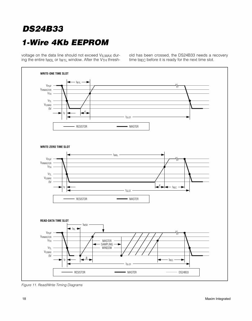
1-Wire 4Kb EEPROMvoltage on the data line should not exceed VILMAX dur-ing the entire tW0L or tW1L window. After the VTH thresh-
old has been crossed, the DS24B33 needs a recoverytime tREC before it is ready for the next time slot.
RESISTOR MASTER
RESISTOR MASTER
RESISTOR MASTER DS24B33
ε
ε
δ
VPUPVIHMASTER
VTH
VTLVILMAX
0VtF
VPUPVIHMASTER
VTH
VTLVILMAX
0V
tF
VPUPVIHMASTER
VTH
VTLVILMAX
0VtF
tSLOT
tW1L
tRECtSLOT
tSLOT
tW0L
tREC
MASTERSAMPLINGWINDOW
tRL
tMSR
WRITE-ONE TIME SLOT
WRITE-ZERO TIME SLOT
READ-DATA TIME SLOT
Figure 11. Read/Write Timing Diagrams
18 Maxim Integrated
DS24B33

1-Wire 4Kb EEPROMSlave-to-Master
A read-data time slot begins like a write-one time slot.The voltage on the data line must remain below VTLuntil the read low time tRL is expired. During the tRL win-dow, when responding with a 0, the DS24B33 startspulling the data line low; its internal timing generatordetermines when this pulldown ends and the voltagestarts rising again. When responding with a 1, theDS24B33 does not hold the data line low at all, and thevoltage starts rising as soon as tRL is over.
The sum of tRL + δ (rise time) on one side and the inter-nal timing generator of the DS24B33 on the other sidedefine the master sampling window (tMSRMIN totMSRMAX) in which the master must perform a read fromthe data line. For the most reliable communication, tRLshould be as short as permissible, and the mastershould read close to but no later than tMSRMAX. Afterreading from the data line, the master must wait untiltSLOT is expired. This guarantees sufficient recoverytime tREC for the DS24B33 to get ready for the next timeslot. Note that tREC specified herein applies only to asingle DS24B33 attached to a 1-Wire line. For multide-vice configurations, tREC needs to be extended toaccommodate the additional 1-Wire device inputcapacitance. Alternatively, an interface that performsactive pullup during the 1-Wire recovery time such asthe DS2482-x00 or DS2480B 1-Wire line drivers can beused.
Improved Network Behavior(Switchpoint Hysteresis)
In a 1-Wire environment, line termination is possibleonly during transients controlled by the bus master(1-Wire driver). 1-Wire networks, therefore, are suscep-tible to noise of various origins. Depending on the phys-ical size and topology of the network, reflections fromend points and branch points can add up or canceleach other to some extent. Such reflections are visibleas glitches or ringing on the 1-Wire communication line.
Noise coupled onto the 1-Wire line from externalsources can also result in signal glitching. A glitch dur-ing the rising edge of a time slot can cause a slavedevice to lose synchronization with the master and,consequently, result in a Search ROM command com-ing to a dead end or cause a device-specific functioncommand to abort. For better performance in networkapplications, the DS24B33 uses an improved 1-Wirefront-end, which makes it less sensitive to noise.
The 1-Wire front-end of the DS24B33 differs from tradi-tional slave devices in one characteristic: There is a hys-teresis at the low-to-high switching threshold VTH. If anegative glitch crosses VTH but does not go belowVTH - VHY, it is not recognized (Figure 12). The hysteresisis effective at any 1-Wire speed.
CRC GenerationThe DS24B33 uses two different types of CRCs. OneCRC is an 8-bit type and is stored in the most signifi-cant byte of the 64-bit registration number. The busmaster can compute a CRC value from the first 56 bitsof the 64-bit registration number and compare it to thevalue stored within the DS24B33 to determine if the reg-istration number has been received error-free. Theequivalent polynomial function of this CRC is X8 + X5 +X4 + 1. This 8-bit CRC is received in the true (noninvert-ed) form. It is computed and programmed into the chipat the factory.
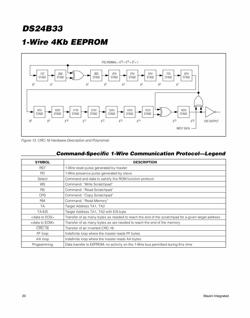
The other CRC is a 16-bit type, generated according tothe standardized CRC-16 polynomial function X16 + X15
+ X2 + 1. This CRC is used for fast verification of a datatransfer when writing to the scratchpad. In contrast tothe 8-bit CRC, the 16-bit CRC is always communicatedin the inverted form. A CRC generator inside theDS24B33 (Figure 13) calculates a new 16-bit CRC, asshown in the command flowchart (Figure 7). The busmaster compares the CRC value read from the deviceto the one it calculates from the data, and decideswhether to continue with an operation.
With the Write Scratchpad command, the CRC is gen-erated by first clearing the CRC generator and thenshifting in the command code, the target addressesTA1 and TA2, and all the data bytes as they were sentby the bus master. The DS24B33 transmits this CRConly if the data bytes written to the scratchpad includescratchpad ending offset 11111b. The data can start atany location within the scratchpad.
For more information on generating CRC values refer toApplication Note 27: Understanding and Using CyclicRedundancy Checks with Maxim iButton Products.
VPUP
VTHVHY
0V
Figure 12. Hysteresis at the Low-to-High Switching Threshold
Maxim Integrated 19
DS24B33
1-Wire 4Kb EEPROM
1STSTAGE
2NDSTAGE
3RDSTAGE
4THSTAGE
7THSTAGE
8THSTAGE
6THSTAGE
5THSTAGE
X0 X1 X2 X3 X4
POLYNOMIAL = X16 + X15 + X2 + 1
INPUT DATA
CRC OUTPUT
X5 X6
11THSTAGE
12THSTAGE
15THSTAGE
14THSTAGE
13THSTAGE
X11 X12
9THSTAGE
10THSTAGE
X9 X10 X13 X14
X7
16THSTAGE
X16X15X8
Figure 13. CRC-16 Hardware Description and Polynomial
SYMBOL DESCRIPTION
RST 1-Wire reset pulse generated by master
PD 1-Wire presence pulse generated by slave
Select Command and data to satisfy the ROM function protocol
WS Command: “Write Scratchpad”
RS Command: “Read Scratchpad”
CPS Command: “Copy Scratchpad”
RM Command: “Read Memory”
TA Target Address TA1, TA2
TA-E/S Target Address TA1, TA2 with E/S byte
<data to EOS> Transfer of as many bytes as needed to reach the end of the scratchpad for a given target address
<data to EOM> Transfer of as many bytes as are needed to reach the end of the memory
CRC-16 Transfer of an inverted CRC-16
FF loop Indefinite loop where the master reads FF bytes
AA loop Indefinite loop where the master reads AA bytes
Programming Data transfer to EEPROM; no activity on the 1-Wire bus permitted during this time
Command-Specific 1-Wire Communication Protocol—Legend
20 Maxim Integrated
DS24B33
1-Wire 4Kb EEPROM
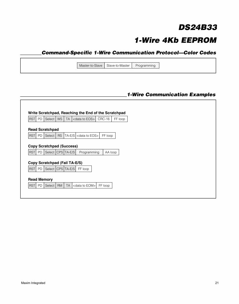
Master-to-Slave Slave-to-Master Programming
Command-Specific 1-Wire Communication Protocol—Color Codes
RST WS
Write Scratchpad, Reaching the End of the Scratchpad
PD TASelect <data to EOS> FF loopCRC-16
Read Scratchpad
Copy Scratchpad (Success)
Copy Scratchpad (Fail TA-E/S)
RST RSPD TA-E/SSelect <data to EOS>
<data to EOM>
FF loop
RST CPSPD TA-E/SSelect FF loop
RST RM TAPD Select FF loop
RST CPSPD TA-E/SSelect AA loop
Read Memory
Programming
1-Wire Communication Examples
Maxim Integrated 21
DS24B33
1-Wire 4Kb EEPROM
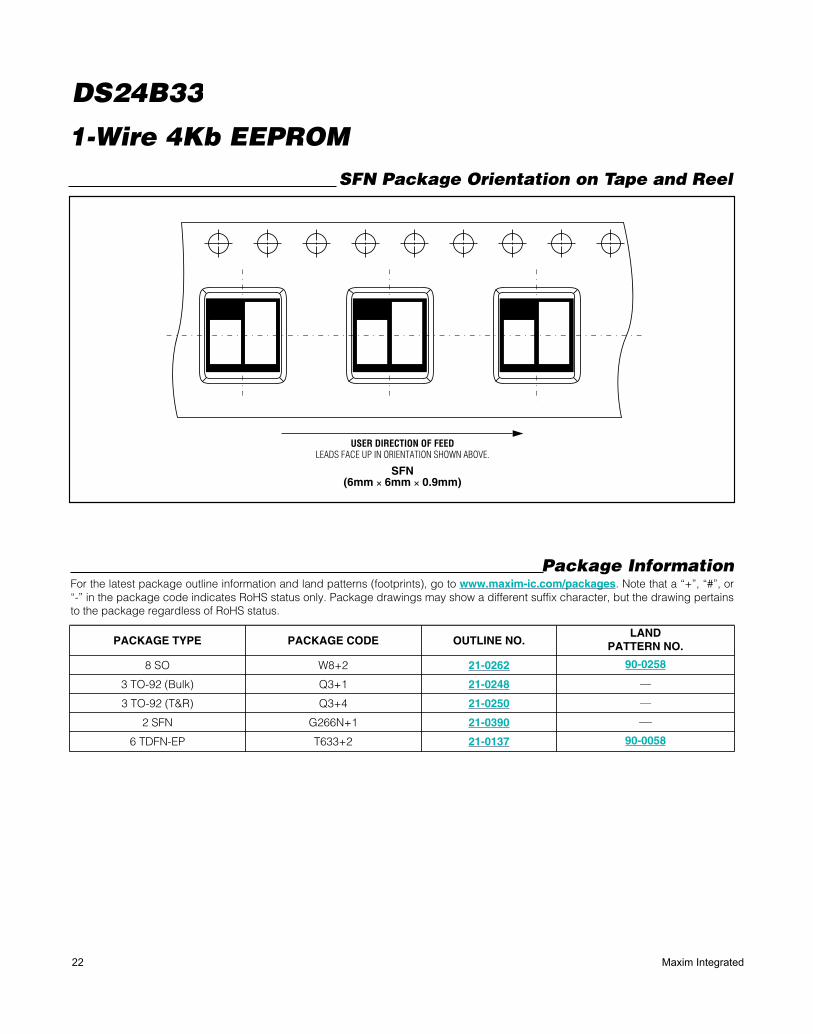
Package InformationFor the latest package outline information and land patterns (footprints), go to www.maxim-ic.com/packages. Note that a “+”, “#”, or“-” in the package code indicates RoHS status only. Package drawings may show a different suffix character, but the drawing pertainsto the package regardless of RoHS status.
USER DIRECTION OF FEEDLEADS FACE UP IN ORIENTATION SHOWN ABOVE.
SFN(6mm × 6mm × 0.9mm)
SFN Package Orientation on Tape and Reel
PACKAGE TYPE PACKAGE CODE OUTLINE NO.LAND
PATTERN NO.
8 SO W8+2 21-0262 90-0258
3 TO-92 (Bulk) Q3+1 21-0248 —
3 TO-92 (T&R) Q3+4 21-0250 —
2 SFN G266N+1 21-0390 —
6 TDFN-EP T633+2 21-0137 90-0058
22 Maxim Integrated
DS24B33
1-Wire 4Kb EEPROMRevision History
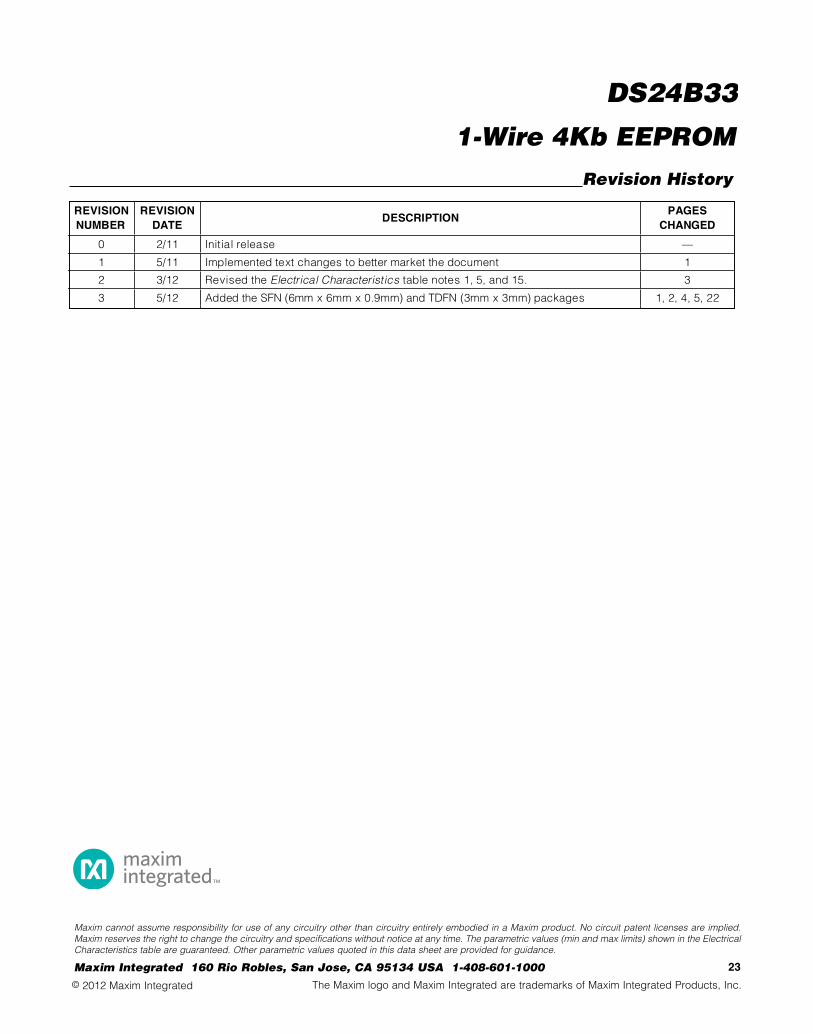
REVISION NUMBER
REVISION DATE
DESCRIPTIONPAGES
CHANGED
0 2/11 Initial release —
1 5/11 Implemented text changes to better market the document 1
2 3/12 Revised the Electrical Characteristics table notes 1, 5, and 15. 3
3 5/12 Added the SFN (6mm x 6mm x 0.9mm) and TDFN (3mm x 3mm) packages 1, 2, 4, 5, 22
23Maxim Integrated 160 Rio Robles, San Jose, CA 95134 USA 1-408-601-1000
Maxim cannot assume responsibility for use of any circuitry other than circuitry entirely embodied in a Maxim product. No circuit patent licenses are implied. Maxim reserves the right to change the circuitry and specifications without notice at any time. The parametric values (min and max limits) shown in the Electrical Characteristics table are guaranteed. Other parametric values quoted in this data sheet are provided for guidance.
© 2012 Maxim Integrated The Maxim logo and Maxim Integrated are trademarks of Maxim Integrated Products, Inc.
DS24B33