Embed Size (px)
Citation preview

November 2017 DocID029159 Rev 2 1/13
This is information on a product in full production. www.st.com
FERD30H100S
100 V field-effect rectifier diode
Datasheet - production data
Features ST advanced rectifier process
Stable leakage current over reverse voltage
Reduced leakage current
Low forward voltage drop
High frequency operation
ECOPACK®2 compliant component
Description The device is based on a proprietary technology that achieves the best in class VF/IR trade-off for a given silicon surface. This 100 V rectifier has been optimized for use in confined casing applications where both efficiency and thermal performance matter. With a lower dependency of leakage current (IR) and forward voltage (VF) in function of temperature, the thermal runaway risk is reduced. Therefore, it can advantageously replace 100 V Schottky diodes.
Table 1: Device summary
Symbol Value
IF(AV) 30 A
VRRM 100 V
VF (max.) 0.405 V
IR(max.) 130 µA
Tj(max.) 175 °C
TO-220AB
DPAK
IPAK
AK
A
K
K
KA
A
A
K
A
K K
AA A
A
Characteristics FERD30H100S
2/13 DocID029159 Rev 2
1 Characteristics Table 2: Absolute ratings (limiting values at 25 °C, unless otherwise specified, with anode
terminals short circuited)
Symbol Parameter Value Unit
VRRM Repetitive peak reverse voltage 100 V
IF(RMS) Forward rms current 45 A
IF(AV) Average forward current δ = 0.5,
square wave TC = 145 °C 30 A
IFSM Surge non repetitive forward current
tp = 10 ms sinusoidal,
DPAK/IPAK 150
A tp = 10 ms sinusoidal,
TO-220AB 250
Tstg Storage temperature range -65 to +175 °C
Tj Maximum operating junction temperature (1) +175 °C
Notes:
(1)(dPtot/dTj) < (1/Rth(j-a)) condition to avoid thermal runaway for a diode on its own heatsink.
Table 3: Thermal resistance parameters
Symbol Parameter Value Unit
Rth(j-c) Junction to case 0.9 °C/W
Table 4: Static electrical characteristics with anode terminals short circuited
Symbol Parameter Test conditions Min. Typ. Max. Unit
IR(1) Reverse leakage current
Tj = 25 °C VR = VRRM
-
130 µA
Tj = 125 °C - 8 16 mA
Tj = 125 °C VR = 70 V - 4 7
VF(2) Forward voltage drop
Tj = 25 °C IF = 3 A
- 0.390 0.440
V
Tj = 125 °C - 0.350 0.405
Tj = 25 °C IF = 5 A
- 0.440 0.495
Tj = 125 °C - 0.415 0.470
Tj = 25 °C IF = 10 A
- 0.550 0.620
Tj = 125 °C - 0.530 0.585
Tj = 125 °C IF = 30 A - 0.680 0.745
Notes:
(1)Pulse test: tp = 5 ms, δ < 2% (2)Pulse test: tp = 380 µs, δ < 2%
To evaluate the conduction losses use the following equation:
P = 0.424 x IF(AV) + 0.0133 IF2(RMS)

FERD30H100S Characteristics
DocID029159 Rev 2 3/13
1.1 Characteristics (curves)
Figure 1: Average forward current versus ambient temperature (δ = 0.5)
Figure 2: Relative variation of thermal impedance junction to case versus pulse duration
Figure 3: Reverse leakage current versus reverse voltage applied (typical values)
Figure 4: Junction capacitance versus reverse voltage applied (typical values)
Figure 5: Forward voltage drop versus forward current (typical values)
Figure 6: Forward voltage drop versus forward current (typical values)
0
5
10
15
20
25
30
35
0 25 50 75 100 125 150 175
Tamb(°C)
T
= tp/T tpδ
IF(AV)(A)
Rth(j-a) = Rth(j-c)
0.0
0.1
0.2
0.3
0.4
0.5
0.6
0.7
0.8
0.9
1.0
1.E-04 1.E-03 1.E-02 1.E-01
tp(s)
Single pulse
Zth(j-c)/Rth(j-c)
1.E-03
1.E-02
1.E-01
1.E+00
1.E+01
1.E+02
0 10 20 30 40 50 60 70 80 90 100
VR(V)
Tj = 125 °C
Tj = 25 °C
Tj = 50 °C
Tj = 75 °C
Tj = 100 °C
Tj = 150 °C
IR(mA)
100
1000
10000
1 10 100
VR(V)
F = 1MHz
Vosc = 30 mVRMSTj = 25 °C
C(pF)
0.1
1.0
10.0
100.0
0.0 0.1 0.2 0.3 0.4 0.5 0.6 0.7 0.8 0.9 1.0
VF(V)
Tj = 25 °C
Tj = 75 °C
Tj = 125 °C
IF(A)
0
10
20
30
0.0 0.1 0.2 0.3 0.4 0.5 0.6 0.7 0.8 0.9 1.0
VF(V)
Tj = 75 °C
Tj = 125 °C
Tj = 25 °C
IF(A)
Characteristics FERD30H100S
4/13 DocID029159 Rev 2
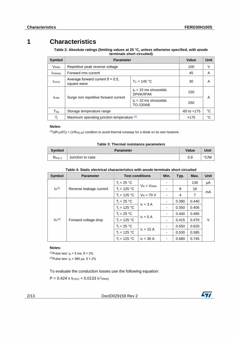
Figure 7: Thermal resistance junction to ambient versus copper surface under tab for DPAK (typical values)
0
10
20
30
40
50
60
70
80
0 5 10 15 20 25 30 35 40
SCu(cm²)
Rth(j-a) (°C/W)
DPAK
Epoxy printed board FR4, eCu= 35 µm
90
100

FERD30H100S Package information
DocID029159 Rev 2 5/13
2 Package information
In order to meet environmental requirements, ST offers these devices in different grades of ECOPACK® packages, depending on their level of environmental compliance. ECOPACK® specifications, grade definitions and product status are available at: www.st.com. ECOPACK® is an ST trademark.
Cooling method: by conduction (C)
Epoxy meets UL94,V0
Recommended torque value: 0.55 N·m (for TO-220AB)
Maximum torque value: 0.6 N·m (for TO-220AB)
Package information FERD30H100S
6/13 DocID029159 Rev 2
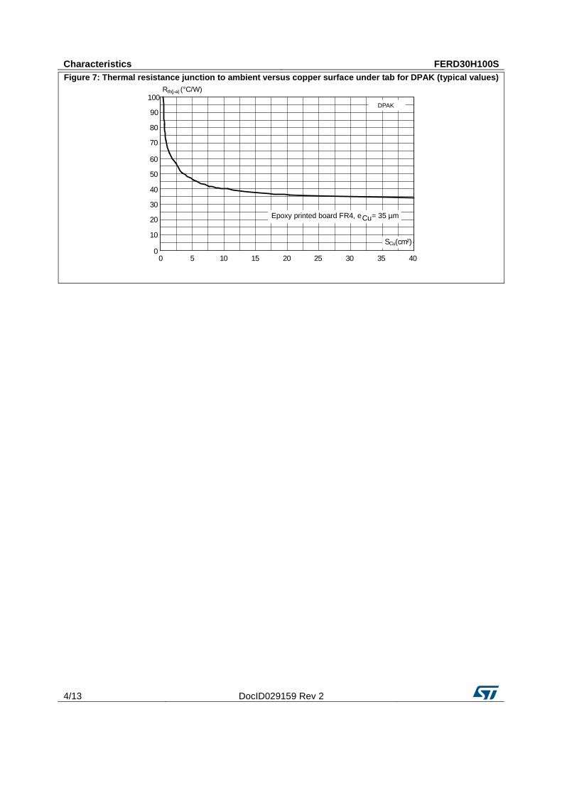
2.1 TO-220AB package information
Figure 8: TO-220AB package outline

FERD30H100S Package information
DocID029159 Rev 2 7/13
Table 5: TO-220AB package mechanical data
Ref.
Dimensions
Millimeters Inches
Min. Max. Min. Max.
A 4.40 4.60 0.173 0.181
b 0.61 0.88 0.024 0.035
b1 1.14 1.70 0.045 0.067
c 0.48 0.70 0.019 0.028
D 15.25 15.75 0.600 0.620
E 10.00 10.40 0.394 0.409
e 2.40 2.70 0.094 0.106
e1 4.95 5.15 0.195 0.203
F 0.51 0.60 0.020 0.024
J1 2.40 2.72 0.094 0.107
H1 6.20 6.60 0.244 0.256
L 13.00 14.00 0.512 0.551
L1 3.50 3.93 0.138 0.155
L20 16.40 typ. 0.646 typ.
L30 28.90 typ. 1.138
Ø P 3.75 3.85 0.148 0.156
Q 2.65 2.95 0.104 0.116

Package information FERD30H100S
8/13 DocID029159 Rev 2
2.2 DPAK package information
Figure 9: DPAK package outline
This package drawing may slightly differ from the physical package. However, all the specified dimensions are guaranteed.

FERD30H100S Package information
DocID029159 Rev 2 9/13
Table 6: DPAK package mechanical data
Ref.
Dimensions
Millimeters Inches
Min. Max. Min. Max.
A 2.18 2.40 0.085 0.094
A1 0.90 1.10 0.035 0.043
A2 0.03 0.23 0.001 0.009
b 0.64 0.90 0.025 0.035
b4 4.95 5.46 0.194 0.215
c 0.46 0.61 0.018 0.024
c2 0.46 0.60 0.018 0.023
D 5.97 6.22 0.235 0.244
D1 4.95 5.60 0.194 0.220
E 6.35 6.73 0.250 0.265
E1 4.32 5.50 0.170 0.216
e 2.286 typ. 0.090 typ.
e1 4.40 4.70 0.173 0.185
H 9.35 10.40 0.368 0.409
L 1.0 1.78 0.039 0.070
L2
1.27
0.050
L4 0.60 1.02 0.023 0.040
V2 -8° +8° -8° +8°
Figure 10: DPAK recommended footprint (dimensions in mm)

Package information FERD30H100S
10/13 DocID029159 Rev 2
2.3 IPAK package information
Figure 11: IPAK package outline

FERD30H100S Package information
DocID029159 Rev 2 11/13
Table 7: IPAK package mechanical data
Ref.
Dimensions
Millimeters Inches
Min. Max. Min. Max.
A 2.20 2.40 0.087 0.094
A1 0.90 1.10 0.035 0.043
b 0.64 0.90 0.025 0.035
b2
0.95
0.037
b4 5.20 5.43 0.205 0.214
B5 0.30 typ. 0.012 typ.
c 0.45 0.60 0.018 0.024
c2 0.46 0.60 0.018 0.024
D 6.00 6.20 0.236 0.244
E 6.40 6.65 0.252 0.261
e 2.28 typ. typ.0.090
e1 4.40 4.60 0.173 0.181
H 16.10 typ. 0.634 typ.
L 9.0 9.60 0.354 0.378
L1 0.80 1.20 0.031 0.047
L2 0.80 typ. 1.25 0.031 typ. 0.049
V1 +10°
+10

Ordering information FERD30H100S
12/13 DocID029159 Rev 2
3 Ordering information Table 8: Ordering information
Order code Marking Package Weight Base qty. Delivery mode
FERD30H100STS FD30H100STS TO-220AB 1.38 g 50 Tube
FERD30H100SH FD30 H100S IPAK 0.32 g 75 Tube
FERD30H100SB-TR FD30 H100S DPAK 0.35 g 2500 Tape and reel
4 Revision history Table 9: Document revision history
Date Revision Changes
07-Apr-2016 1 Initial release.
14-Nov-2017 2 Updated cover page.
FERD30H100S
DocID029159 Rev 2 13/13
IMPORTANT NOTICE – PLEASE READ CAREFULLY
STMicroelectronics NV and its subsidiaries (“ST”) reserve the right to make changes, corrections, enhancements, modifications , and improvements to ST products and/or to this document at any time without notice. Purchasers should obtain the latest relevant information on ST products before placing orders. ST products are sold pursuant to ST’s terms and conditions of sale in place at the time of order acknowledgement.
Purchasers are solely responsible for the choice, selection, and use of ST products and ST assumes no liability for application assistance or the design of Purchasers’ products.
No license, express or implied, to any intellectual property right is granted by ST herein.
Resale of ST products with provisions different from the information set forth herein shall void any warranty granted by ST for such product.
ST and the ST logo are trademarks of ST. All other product or service names are the property of their respective owners.
Information in this document supersedes and replaces information previously supplied in any prior versions of this document.
© 2017 STMicroelectronics – All rights reserved