Embed Size (px)
Citation preview
16
1.1. INTRODUCTION TO MICROPROCESSOR, MICROCONTROLLER AND
SYSTEM DESIGN
The brain or engine of the PC is the processor (sometimes called microprocessor), or central
processing unit (CPU). The CPU performs the system’s calculating and processing. The processor is easily
the most expensive single component in the system, costing up to four or more times greater than the motherboard it plugs into. Intel is generally credited with creating the first microprocessor in 1971 with the introduction of a chip called the 4004.
Today Intel still has control over the processor market, at least for PC systems. This means that all PC-compatible systems use either Intel processors or Intel-compatible processors from a handful of competitors (such as AMD or Cyrix). Intel’s dominance in the processor market had not always been assured. Although Intel is generally credited with inventing the processor and introducing the first one on the market, by the late 1970s the two most popular processors for PCs were not from Intel (although one was a clone of an Intel processor). Personal computers of that time primarily used the Z-80 by Zilog and the 6502 by MOS Technologies. The Z-80 was noted for being an improved and less expensive clone of the Intel 8080 processor, similar to the way companies today such as AMD, Cyrix, IDT, and Rise Technologies have cloned Intel’s Pentium processors. In that case though, the clone had become more popular than the
original. The Z-80 was used in systems of the late 1970s and early1980s that ran the CP/M operating system, while the 6502 was best known for its use in the early Apple computers (before the Mac). The fate of both Intel and Microsoft was dramatically changed in 1981 when IBM introduced the IBM PC, which was based on a 4.77MHz Intel 8088 processor running the Microsoft Disk Operating System (MS-DOS) 1.0. 1.1.1. Pre-PC Microprocessor History
The microprocessor was invented by Intel in 1971. The PC was created by IBM in 1981. The
processors powering our PCs today are still backward compatible in many ways with the 8088 selected by IBM in 1981. The 4004 processor was introduced on November 15, 1971, and originally ran at a clock speed of 108KHz (108,000 cycles per second, or just over one-tenth a megahertz). The 4004 contained 2,300 transistors and was built on a 10 micron process. Data was transferred four bits at a time, and the maximum addressable memory was only 640 bytes. The 4004 was designed for use in a calculator, but proved to be useful for many other functions because of its inherent programmability. In April 1972, Intel released the 8008 processor, which originally ran at a clock speed of 200KHz (0.2MHz). The 8008 processor contained 3,500 transistors and was built on the same 10 micron process as the previous processor. The big change in the 8008 was that it had an 8-bit data bus, which meant it could move data 8 bits at a time—twice as much as the previous chip. It could also address more memory, up to 16KB. This chip was primarily used in dumb terminals and general-purpose calculators. The next chip in the lineup was the 8080, introduced in April 1974, running at a clock rate of 2MHz.Due mostly to the faster clock rate, the 8080 processor had 10 times the performance of the 8008. The 8080 chip contained 6,000 transistors and was built on a 6 micron process. Like the previous chip, the 8080 had an 8-bit data bus, so it could transfer 8 bits of data at a time. The 8080 could address up to 64KB of memory, significantly more than the previous chip. It was the 8080 that helped start the PC revolution, as this was the processor chip used in what is generally regarded as the first personal computer, the Altair 8800. The CP/M operating system was written for the 8080 chip, and Microsoft was founded and delivered its first product: Microsoft BASIC for the Altair. These initial tools provided the foundation for a revolution in software because thousands of programs were written to run on this platform
17
The Z-80 also incorporated a superset of 8080 instructions, meaning it could run all 8080 programs. It also included new instructions and new internal registers, so software that was designed for the Z-80 would not necessarily run on the older 8080. The Z-80 ran initially at 2.5MHz (later versions ran up to 10MHz), and contained 8,500 transistors. The Z-80 could access 64KB of memory.
Intel released the 8085, its follow up to the 8080, in March of 1976. The 8085 ran at 5MHz and contained 6,500 transistors. It was built on a 3-micron process and incorporated an 8-bit data bus. Along different architectural lines, MOS Technologies introduced the 6502 in 1976. The chip was used in Apple I and Apple II design and systems by Commodore and other system manufacturers. The 6502 and its successors were also used in computer games, including the original Nintendo Entertainment System (NES) among others. Motorola went on to create the 68000 series, which became the basis for the Apple Macintosh line of computers. Intel introduced the 8086 in June 1978.The 8086 chip brought with it the original x86 instruction set that is still present on x86-compatible chips such as the Pentium III. A dramatic improvement over the previous chips, the 8086 was a full 16-bit design with 16-bit internal registers and a 16-bit data bus. This meant that it could work on 16- bit numbers and data internally and also transfer 16-bits at a time in and out of the chip. The 8086contained 29,000 transistors and initially ran at up to 5MHz. The chip also used 20-bit addressing,meaning it could directly address up to 1MB of memory. In 1979, Intel released a crippled version of the 8086 called the 8088. The 8088 processor used the same internal core as the 8086, had the same 16-bit registers, and could address the same 1MB of memory, but the external data bus was reduced to 8 bits. This allowed support chips from the older 8-bit 8085 to be used, and far less expensive boards and systems could be made. It is for these reasons that IBM chose the crippled chip, the 8088, for the first PC.
This decision would affect history in several ways. The 8088 was fully software compatible with the 8086, so it could run 16-bit software. Also, because the instruction set was very similar to the previous 8085 and 8080, programs written for those older chips could be quickly and easily modified to run. This allowed a large library of programs to be quickly released for the IBM PC, thus helping it become a success. The overwhelming blockbuster success of the IBM PC left in its wake the legacy of requiring backward compatibility with it. In order to maintain the momentum, Intel has pretty much been forced to maintain backward compatibility with the 8088/8086 in most of the processors it has released since then. In some ways the success of the PC, and the Intel architecture it contains, has limited the growth of the personal computer. In other ways, however, its success has caused a huge number of programs, peripherals, and accessories to be developed, and the PC to become a de facto standard in the industry. The original 8088 processor used in the first PC contained close to 30,000 transistors and ran at less than 5MHz. Intel recently introduced a version of the Pentium III Xeon with 2MB of on die cache that has a whopping 140 million transistors, the largest ever in a single processor chip. Both AMD and Intel are manufacturing processors that run at 1GHz (AMD has some bragging rights there; it beat Intel to 1GHz by two days), and both have demonstrated processors running in the 2GHz range. And the progress doesn’t stop there, as
according to Moore’s Law, processing speed and transistor counts are doubling every 1.5 to 2 years.
1.1.2. Processor Specifications
Many confusing specifications often are quoted in discussions of processors. The following sections discuss some of these specifications, including the data bus, address bus, and speed. Processors can be identified by two main parameters: how wide they are and how fast they are. The speed of a processor is a fairly simple concept. Speed is counted in megahertz (MHz), which means millions of cycles per second—
and faster is better They are l Internal registers
18
l Data input and output bus l Memory address bus
`Systems below 16MHz usually had no cache memory at all. Starting with 16MHz systems, highspeed cache memory appeared on the motherboard because the main memory at the time could not run at 16MHz. Prior to the 486 processor, the cache on the motherboard was the only cache used in the system. Starting with the 486 series, processors began including what was called L1 (Level 1) cache directly on the processor die. This meant that the L1 cache always ran at the full speed of the chip, especially important when the later 486 chips began to run at speeds higher than the motherboards they were plugged into. During this time the cache on the motherboard was called the second level or L2 cache, which ran at the slower motherboard speed. Starting with the Pentium Pro and Pentium II, Intel began including L2 cache memory chips directly within the same package as the main processor. Originally this built-in L2 cache was implemented as physically separate chips contained within the processor package but not a part of the processor die. Since the speed of commercially available cache memory chips could not keep pace with the main processor, most of the L2 cache in these processors ran at one-half speed (Pentium II/III and AMD Athlon), while some ran the cache even slower, at two-fifths or even one-third the processor speed (AMD Athlon).
1.1.3. Brief History of Multi-core CPUs
Multi-core processing has been at the heart of the computing revolution for more than a decade. The transition began with server CPU manufacturers adopting multi-core processor architectures to address growing performance demands, combined with the dramatic increase in power consumption of single core processors running at high frequencies. Multi-core CPUs can operate at lower frequency, often consuming less power, and completing work much faster by running tasks in parallel compared to single core predecessors.
1.2. MICROPROCESSOR AND MICROCONTROLLER AS A PROGRA-
MMABLE DEVICE
1.2.1. COMPUTER ORGANIZATION AND TYPICAL MICROPROCESSOR
The CPU executes a sequence of instructions.The execution of an instruction is organized as an instruction cycle. it is performed as a succession of several steps.Each step is executed as a set of several microoperations.A basic computer organization block diagram is given below • The task performed by any microoperation falls in one of the following categories:
- Transfer data from one register to another; - Transfer data from a register to an external interface (system bus); - Transfer data from an external interface to a register; - Perform an arithmetic or logic operation, using registers for input and output.
In order to allow the execution of a microoperation, one or several control signals have to be issued; they allow the corresponding data transfer and/or computation to be performed. The CPU executes an instruction as a sequence of control steps. In each control step one or several microoperations are executed. • One clock pulse triggers the activities corresponding to one control step for each clock pulse the control unit generates the control signals corresponding to the microoperations to be executed in the respective control step.
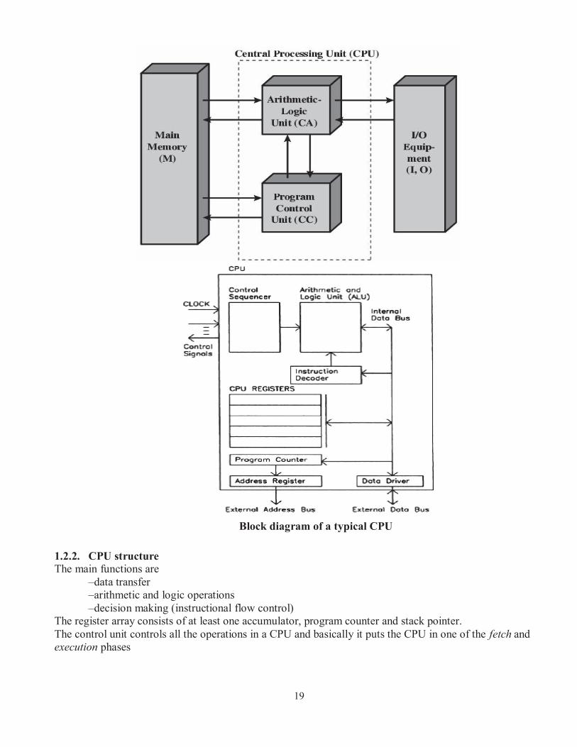
19
Block diagram of a typical CPU
1.2.2. CPU structure
The main functions are –data transfer –arithmetic and logic operations –decision making (instructional flow control)
The register array consists of at least one accumulator, program counter and stack pointer. The control unit controls all the operations in a CPU and basically it puts the CPU in one of the fetch and execution phases
20
1.2.3. Microprocessor
A microprocessor incorporates the functions of a computer's central processing unit (CPU) on a single integrated circuit (IC), or at most a few integrated circuits. It is a multipurpose, programmable device that accepts digital data as input, processes it according to instructions stored in its memory, and provides results as output. It is an example of sequential digital logic, as it has internal memory. Microprocessors operate on numbers and symbols represented in the binary numeral system. The advent of low-cost computers on integrated circuits has transformed modern society. General-purpose microprocessors in personal computers are used for computation, text editing, multimedia display, and communication over the Internet. Many more microprocessors are part of embedded systems, providing digital control over myriad objects from appliances to automobiles to cellular phones and industrial process control.
1.2.4. ALU
In computing, an arithmetic and logic unit (ALU) is a digital circuit that performs integer arithmetic and logical operations. The ALU is a fundamental building block of the central processing unit of a computer, and even the simplest microprocessors contain one for purposes such as maintaining timers. The processors found inside modern CPUs and graphics processing units (GPUs) accommodate very powerful and very complex ALUs; a single component may contain a number of ALUs. Mathematician John von Neumann proposed the ALU concept in 1945, when he wrote a report on the foundations for a new computer called the EDVAC. Research into ALUs remains as an important part of computer science, falling under Arithmetic and logic structures in the ACM Computing Classification System.
Most of a processor's operations are performed by one or more ALUs. An ALU loads data from input registers. Then an external control unit tells the ALU what operation to perform on that data, and then the ALU stores its result into an output register. The control unit is responsible for moving the processed data between these registers, ALU and memory.
1.2.5. Control unit
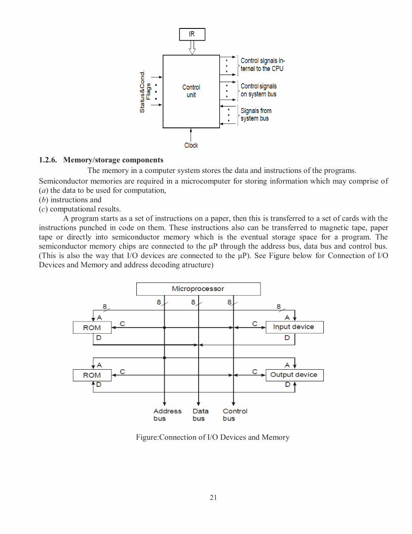
The basic task of the control unit: - for each instruction the control unit causes the CPU to go through a sequence of control steps; - in each control step the control unit issues a set of signals which cause the corresponding microoperations to be executed. • The control unit is driven by the processor clock. The signals to be generated at a certain moment depend on: - the actual step to be executed; - the condition and status flags of the processor; - the actual instruction executed; - external signals received on the system bus (e.g. interrupt signals).
21
1.2.6. Memory/storage components
The memory in a computer system stores the data and instructions of the programs.
Semiconductor memories are required in a microcomputer for storing information which may comprise of (a) the data to be used for computation, (b) instructions and (c) computational results.
A program starts as a set of instructions on a paper, then this is transferred to a set of cards with the instructions punched in code on them. These instructions also can be transferred to magnetic tape, paper tape or directly into semiconductor memory which is the eventual storage space for a program. The semiconductor memory chips are connected to the μP through the address bus, data bus and control bus.
(This is also the way that I/O devices are connected to the μP). See Figure below for Connection of I/O Devices and Memory and address decoding atructure)
Figure:Connection of I/O Devices and Memory
22
1.2.6.1. Main memory types
Memories may be broadly divided into two classes: (a) Random Access Memory (RAM) or Read/Write Memory (RWM)
There is provision in RAMs (RWMs) for writing information into the memory and reading it when the microcomputer is in operation. It is, therefore, used to store information which changes or may change
23
during the operation of the system, viz. data for calculations and results of calculations. It is also used to store the programs which are to be changed frequently. Semiconductor RAM is a volatile memory.
A RAM can be of static or dynamic type. Dynamic RAMs have higher packing densities, are faster and consume less power in the quiescent state. However, because of external refreshing circuitry requirement, the dynamic RAMs are profitable only in large sizes.
(b) Read-Only Memory (ROM)
The ROM functions as a memory array whose contents once programmed, are permanently fixed and can not be altered by the μP while the system is operating. It is non-volatile. ROMs exist in many forms. (i) Mask ROM : It is custom programmed or mask programmed when manufactured and can not be altered thereafter. The cost of a custom built mask for programming is so high that thousands of ROMs storing the same information must be produced to pay for the mask. (ii) Programmable ROM (PROM) : This type is programmable by the user (typically by electrically overheating fusible links in selected manner). Once programmed, the contents can not be altered. The memory may be programmed one at a time by the user and is thus suitable for the cases where small quantities of a ROM are needed. (iii) Electrically Alterable ROM (EAROM) : In this type of memory, the contents can be electrically erased (by applying a large negative voltage to control gates of memory cells) and the memory can be then reprogrammed (by applying a large positive voltage to control gates). This type is convenient when the user is not sure of the program and may wish to modify it. This is a typical requirement in prototype development. (iv) Erasable Programmable ROM (EPROM) : Like EAROM, this type of memory can also be erased and reprogrammed. However, erasing is by exposing the memory chips to high intensity ultravoilet light of a wavelength close to 2537 Å. It has the same application filed as the EAROM. 1.2.6.2. Bipolar v/s MOS Memories
Basically there are two semiconductor technologies, namely, bipolar and MOS unipolar. Mask ROMs and PROMs are available in both types whereas EAROMs and EPROMs are made with MOS technology only. In general, bipolar devices (including memories) are faster and have higher drive capabilities. On the other hand, MOS devices consume less space and power and are cheaper. Therefore, MOS memories are preferred where speed is not a critical factor. The following table summarizes the characteristics of the various kinds of data storage in the storage hierarchy.
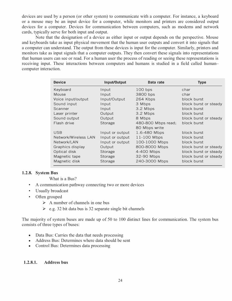
1.2.7. Input and Output
In computing, input/output or I/O is the communication between an information processing system
(such as a computer) and the outside world, possibly a human or another information processing system. Inputs are the signals or data received by the system, and outputs are the signals or data sent from it. The term can also be used as part of an action; to "perform I/O" is to perform an input or output operation. I/O
24
devices are used by a person (or other system) to communicate with a computer. For instance, a keyboard or a mouse may be an input device for a computer, while monitors and printers are considered output devices for a computer. Devices for communication between computers, such as modems and network cards, typically serve for both input and output.
Note that the designation of a device as either input or output depends on the perspective. Mouse and keyboards take as input physical movement that the human user outputs and convert it into signals that a computer can understand. The output from these devices is input for the computer. Similarly, printers and monitors take as input signals that a computer outputs. They then convert these signals into representations that human users can see or read. For a human user the process of reading or seeing these representations is receiving input. These interactions between computers and humans is studied in a field called human–
computer interaction.
1.2.8. System Bus
What is a Bus?
• A communication pathway connecting two or more devices
• Usually broadcast
• Often grouped Ø A number of channels in one bus
Ø e.g. 32 bit data bus is 32 separate single bit channels
The majority of system buses are made up of 50 to 100 distinct lines for communication. The system bus consists of three types of buses:
Data Bus: Carries the data that needs processing Address Bus: Determines where data should be sent Control Bus: Determines data processing
1.2.8.1. Address bus
25
The address bus is the set of wires that carries the addressing information used to describe the memory location to which the data is being sent or from which the data is being retrieved. As with the data bus, each wire in an address bus carries a single bit of information. This single bit is a single digit in the address. The more wires (digits) used in calculating these addresses, the greater the total number of address locations. The size (or width) of the address bus indicates the maximum amount of RAM that a chip can address.
1.2.8.2. Data bus
The size of the internal registers indicate how much information the processor can operate on at one
time and how it moves data around internally within the chip. This is sometimes also referred to as the internal data bus. The register size is essentially the same as the internal data bus size. A register is a holding cell within the processor; for example, the processor can add numbers in two different registers, storing the result in a third register. The register size determines the size of data the processor can operate on. The register size also describes the type of software or commands and instructions a chip can run. That is, processors with 32-bit internal registers can run 32-bit instructions that are processing 32-bit chunks of data, but processors with 16-bit registers cannot. Most advanced processors today—chips from the 386 to the Pentium III—use 32-bit internal registers and can therefore run the same 32-bit operating systems and software.
1.2.8.3. Control bus
A control bus is a computer bus that is used by the CPU to communicate with devices that are contained within the computer. This occurs through physical connections such as cables or printed circuits. The CPU transmits a variety of control signals to components and devices to transmit control signals to the CPU using the control bus. One of the main objectives of a bus is to minimize the lines that are needed for communication. An individual bus permits communication between devices using one data channel. The control bus is bidirectional and assists the CPU in synchronizing control signals to internal devices and external components. It is comprised of interrupt lines, byte enable lines, read/write signals and status lines.
Communication between the CPU and control bus is necessary for running a proficient and functional system. Without the control bus the CPU cannot determine whether the system is receiving or sending data. It is the control bus that regulates which direction the write and read information need to go. The control bus contains a control line for write instructions and a control line for read instructions. When the CPU writes data to the main memory, it transmits a signal to the write command line. The CPU also sends a signal to the read command line when it needs to read. This signal permits the CPU to receive or transmit data from main memory.
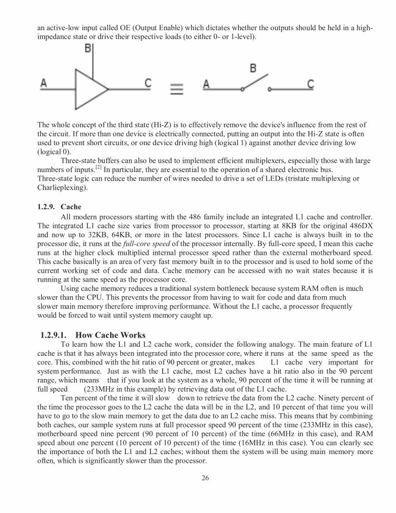
1.2.8.4. Tristate bus
In digital electronics three-state, tri-state, or 3-state logic allows an output port to assume a high impedance state in addition to the 0 and 1 logic levels, effectively removing the output from the circuit. This allows multiple circuits to share the same output line or lines (such as a bus which cannot listen to more than one device at a time). Three-state outputs are implemented in many registers, bus drivers, and flip-flops in the 7400 and 4000 series as well as in other types, but also internally in many integrated circuits. Other typical uses are internal and external buses in microprocessors, memories, and peripherals. Many devices are controlled by
26
an active-low input called OE (Output Enable) which dictates whether the outputs should be held in a high-impedance state or drive their respective loads (to either 0- or 1-level).
The whole concept of the third state (Hi-Z) is to effectively remove the device's influence from the rest of the circuit. If more than one device is electrically connected, putting an output into the Hi-Z state is often used to prevent short circuits, or one device driving high (logical 1) against another device driving low (logical 0).
Three-state buffers can also be used to implement efficient multiplexers, especially those with large numbers of inputs.[2] In particular, they are essential to the operation of a shared electronic bus. Three-state logic can reduce the number of wires needed to drive a set of LEDs (tristate multiplexing or Charlieplexing).
1.2.9. Cache
All modern processors starting with the 486 family include an integrated L1 cache and controller. The integrated L1 cache size varies from processor to processor, starting at 8KB for the original 486DX and now up to 32KB, 64KB, or more in the latest processors. Since L1 cache is always built in to the processor die, it runs at the full-core speed of the processor internally. By full-core speed, I mean this cache runs at the higher clock multiplied internal processor speed rather than the external motherboard speed. This cache basically is an area of very fast memory built in to the processor and is used to hold some of the current working set of code and data. Cache memory can be accessed with no wait states because it is running at the same speed as the processor core.
Using cache memory reduces a traditional system bottleneck because system RAM often is much slower than the CPU. This prevents the processor from having to wait for code and data from much slower main memory therefore improving performance. Without the L1 cache, a processor frequently would be forced to wait until system memory caught up.
1.2.9.1. How Cache Works To learn how the L1 and L2 cache work, consider the following analogy. The main feature of L1
cache is that it has always been integrated into the processor core, where it runs at the same speed as the core. This, combined with the hit ratio of 90 percent or greater, makes L1 cache very important for system performance. Just as with the L1 cache, most L2 caches have a hit ratio also in the 90 percent range, which means that if you look at the system as a whole, 90 percent of the time it will be running at full speed (233MHz in this example) by retrieving data out of the L1 cache.
Ten percent of the time it will slow down to retrieve the data from the L2 cache. Ninety percent of the time the processor goes to the L2 cache the data will be in the L2, and 10 percent of that time you will have to go to the slow main memory to get the data due to an L2 cache miss. This means that by combining both caches, our sample system runs at full processor speed 90 percent of the time (233MHz in this case), motherboard speed nine percent (90 percent of 10 percent) of the time (66MHz in this case), and RAM speed about one percent (10 percent of 10 percent) of the time (16MHz in this case). You can clearly see the importance of both the L1 and L2 caches; without them the system will be using main memory more often, which is significantly slower than the processor.
27
1.2.10. PERIPHERAL INTERFACING
1.2.10.1. Functions When one or more I/O devices (peripherals) are to be connected to a for each device, called peripheral interface, is required. The interface incorporate commonly the following four functions: (a) Buffering peripheral. (b) Address Decoding : Which is required to select one of the several peripherals connected in the system.
(c) Command Decoding : Which is required for peripherals that perform actions other than data transfers. (d) Timing and Control : All the above functions require timing and control.
1.3. BASIC CPU ARCHITECTURES
1.3.1. CISC vs. RISC
There are two types of fundamental CPU architecture: complex instruction set computers (CISC) and
reduced instruction set computers (RISC). CISC is the most prevalent and established microprocessor
architecture, while RISC is a relative newcomer. Intel’s 80x86 and Pentium microprocessor families are
CISC-based, although RISC-type functionality has been incorporated into Pentium CPUs. Motorola’s
68000 family of microprocessors is another example of this type of architecture. Sun Microsystems’
SPARC microprocessors and MIPS R2000, R3000 and R4000 families dominate the RISC end of the
market; however, Motorola’s PowerPC, G4, Intel’s i860, and Analog Devices Inc.’s digital signal
processors (DSP) are in wide use. In the PC/Workstation market, Apple Computers and Sun employ RISC microprocessors as their choice of CPU.`
Table 1 CISC and RISC
CISC RISC
Large instruction set Compact instruction set
Complex, powerful instructions Simple hard-wired machine code and control unit
Instruction sub-commands micro-coded in on board ROM
Pipelining of instructions
Compact and versatile register set Numerous registers
Numerous memory addressing options for operands
Compiler and IC developed simultaneously
The difference between the two architectures is the relative complexity of the instruction sets and
underlying electronic and logic circuits in CISC microprocessors. For example, the original RISC I
prototype had just 31 instructions, while the RISC II had 39. In the RISC II prototype, these instructions are
hard-wired into the microprocessor using 41,000 integrated transistors, so that when a program instruction
is presented for execution it can be processed immediately. This typifies the pure RISC approach, which results in up-to-a fourfold increase in processing power over comparable CISC processors.
28
In contrast, the Intel 386 has 280,000 and uses microcode stored in on-board ROM to process the instructions. Complex instructions have to be first decoded in order to identify which microcode routine needs to be executed to implement the instructions. The Pentium II used 9.5 million transistors and while older microcode is retained, the most frequently used and simpler instructions, such as MMX, are hardwired. Thus Pentium CPUs are essentially a hybrid, however they are still classified as RISC as their basic instructions are complex.
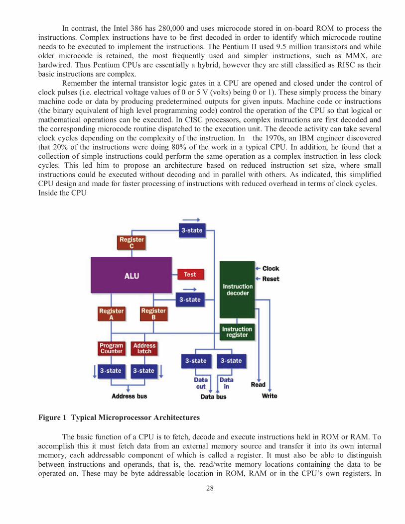
Remember the internal transistor logic gates in a CPU are opened and closed under the control of clock pulses (i.e. electrical voltage values of 0 or 5 V (volts) being 0 or 1). These simply process the binary machine code or data by producing predetermined outputs for given inputs. Machine code or instructions (the binary equivalent of high level programming code) control the operation of the CPU so that logical or mathematical operations can be executed. In CISC processors, complex instructions are first decoded and the corresponding microcode routine dispatched to the execution unit. The decode activity can take several clock cycles depending on the complexity of the instruction. In the 1970s, an IBM engineer discovered that 20% of the instructions were doing 80% of the work in a typical CPU. In addition, he found that a collection of simple instructions could perform the same operation as a complex instruction in less clock cycles. This led him to propose an architecture based on reduced instruction set size, where small instructions could be executed without decoding and in parallel with others. As indicated, this simplified CPU design and made for faster processing of instructions with reduced overhead in terms of clock cycles. Inside the CPU
Figure 1 Typical Microprocessor Architectures
The basic function of a CPU is to fetch, decode and execute instructions held in ROM or RAM. To accomplish this it must fetch data from an external memory source and transfer it into its own internal memory, each addressable component of which is called a register. It must also be able to distinguish between instructions and operands, that is, the. read/write memory locations containing the data to be operated on. These may be byte addressable location in ROM, RAM or in the CPU’s own registers. In
29
addition, the CPU must perform additional tasks such as responding to external events such as resets and interrupts, provide memory management facilities to the operating system, etc. A consideration of the fundamental components in a basic microprocessor is first undertaken before introducing more complex modern devices. Figure 6 illustrates a typical microprocessor architecture Microprocessors must perform the following activities:
Provide temporary storage for addresses and data Perform arithmetic and logic operations Control and schedule all operations.
1.3.2. Registers
Registers for a variety of purposes such as holding the address of instructions and data, storing the result of an operation, signaling the result of a logic operation, or indicating the status of the program or the CPU itself. Some registers may be accessible to programmers, while others are reserved for us by the CPU itself. Registers store binary values such as 1 or 0 as electrical voltages of say 5 volts (or less) or 0 volts. They consist of several integrated transistors which are configured as a flip-flop circuits each of which can be switched into a 1 or 0 state. They remain in that state until changed under control of the CPU or until the power is removed from the processor. Each register has a specific name and is addressable, some, however, are dedicated to specific tasks while the majority are ‘general purpose’. The width of a register
depends on the type of CPU, e.g., a 16, 32 or 64 bit microprocessor. In order to provide backward compatibility, registers may be sub-divided. For example, the Pentium processor is a 32 bit CPU, and its registers are 32 bits wide. Some of these are sub-divided and named as 8 and 16 bit registers in order to run 8 and 16 bit applications designed for earlier x86 microprocessors.
1.3.3. Instruction Register
When the Bus Interface Unit receives an instruction it transfers it to the Instruction Register for temporary storage. In Pentium processors the Bus Interface Unit transfers instructions to the L1 I-Cache, there is no instruction register as such. 1.3.4. Stack Pointer
A ‘stack’ is a small area of reserved memory used to store the data in the CPU’s registers when: (1) system
calls are made by a process to operating system routines; (2) when hardware interrupts generated by input/output (I/O) transactions on peripheral devices; (3) when a process initiates an I/O transfer; and (4) when a process rescheduling event occurs on foot of a hardware timer interrupt. This transfer of register contents is called a ‘context switch’. The stack pointer is the register which holds the address of the most recent ‘stack’ entry. Hence, when a system call is made by a process (to say print a document) and its
context is stored on the stack, the called system routine uses the stack pointer to reload the register contents when it is finished printing. Thus the process can continue where it left off. 1.3.5. Instruction Decoder
The Instruction Decoder is an arrangement of logic elements which act on the bits that constitute the instruction. Simple instructions with corresponding logic hard-wired into the execution unit are simply passed to the Execution Unit (and/or the MMX in the Pentium II, III and IV), complex instructions are decoded so that related microcode modules can be transferred from the CPU’s microcode ROM to the execution unit. The Instruction Decoder will also store referenced operands in appropriate registers so data at the memory locations referenced can be fetched. 1.3.6. Program or Instruction Counter
30
The Program Counter (PC) is the register that stores the address in primary memory (RAM or ROM) of the next instruction to be executed. In 32 bit systems, this is a 32 bit linear or virtual memory address that references a byte (the first of 4 required to store the 32 bit instruction) in the process’s virtual memory address space. This value is translated to determine the real memory address in which the instruction is stored. When the referenced instruction is fetched, the address in the PC is incremented to the address of the next instruction to be executed. Remember each byte in RAM is individually addressable, however each complete instruction is 32 bits or 4 bytes, and the address of the next instruction in the process will be 4 bytes on.
1.3.7. Accumulator
The accumulator may contain data to be used in a mathematical or logical operation, or it may contain the result of an operation. General purpose registers are used to support the accumulator by holding data to be loaded to/from the accumulator. 1.3.8. Computer Status Word (CSW) or Flag Register
The result of a ALU operation may have consequences of subsequent operations; for example, changing the path of execution. Individual bits in the CSW are set or reset in accordance with the result of mathematical or logical operations. Also called a flag, each bit in the register has a pre-assigned meaning and the contents are monitored by the control unit to help control CPU related actions. 1.3.9. Arithmetic and Logic Unit
The Arithmetic and Logic Unit (ALU) performs all arithmetic and logic operations in a microprocessor viz. addition, subtraction, logical AND, OR, EX-OR, etc. A typical ALU is connected to the accumulator and general purpose registers and other CPU components that help transfer the result of its operations to RAM via the Bus Interface Unit and the system bus. The results may also be written into internal or external caches. 1.3.10. Control Unit
The control unit coordinates and manages CPU activities, in particular the execution of instructions by the arithmetic and logic unit (ALU). In Pentium processors its role is complex, as microcode from decoded instructions are pipelined for execution by two ALUs. 1.3.11. The System Clock
The Intel 8088 CPU had a clock speed of 4.77 MHz; that is, its internal logic gates were opened and closed under the control of a square wave pulsed signal that had a frequency of 4.77 million cycles per second. Alternatively put, the logic gates opened and closed 4.77 million times per second. Thus, instructions and data were pumped through the integrated transistor logic circuits at a rate of 4.77 million times per second. Later designs ran at higher speeds viz. the i286 8-20 MHz, the i386 16-33 MHz, i486 25-50 MHz. Where does this clock signal come from? Each motherboard is fitted with a quartz oscillator in a metal package that generates a square wave clock pulse of a certain frequency. In i8088 systems the crystal oscillator ran at 14.318 MHz and this was fed to the i8284 to generate the system clock frequency of 4.77 MHz in earlier system, to 10 MHz is later designs. Later, the i286 PCs had a 12 MHz crystal which provided i82284 IC multiplier/divider with the primary clock signal. This then divided/multiplied the basic 12 MHz to generate the system clock signal of 8-20 MHz. With the advent of the i486DX, the system clock signal, which ran at 25 or 33 MHz, was effectively multiplied by factors of 2, 3 or more to deliver an internal CPU clock speed
31
of 50, 66, 75, 100 MHz. This approach is used in Pentium IV architectures, where the primary crystal source delivers a relatively slow 50 MHz clock signal that is then multiplied to the system clock speed of 100-133 MHz. The internal multiplier in the Pentium then multiplies this by a fact or 20+ to obtain speeds of 2 Ghz and above. 1.3.12. Instruction Cycle
An instruction cycle consists of the activities required to fetch and execute an instruction. The length of time take to fetch and execute is measured in clock cycles. In CISC processors this will take many clock cycles, depending on the complexity of the instruction and number of memory references made to load operands. In RISC computers the number of clock cycles are reduced significantly. When the CPU finishes the execution of an instruction it transfers the content of the program or instruction register into the Bus Interface Unit (1 clock cycle) . This is then gated onto the system address bus and the read signal is asserted on the control bus (1 clock cycle). This is a signal to the RAM controller that the value of this address is to be read from memory and loaded onto the data bus (4+ clock cycles). The instruction is read in from the data bus and decoded (2 + clock cycles). The fetch and decode activities constitute the first machine cycle of the instruction cycle. The second machine cycle begins when the instruction’s operand is read from
RAM and ends when the instruction is executed and the result written back to memory. This will take at least another 8+ clock cycles, depending on the complexity of the instruction. Thus an instruction cycle will take at least 16 clock cycles, a considerable length of time. Together, RISC processors and fast RAM can keep this to a minimum. However, Intel made advances by super pipelining instructions, that is by interleaving fetch, decode, operand read, execute, and retire (i.e. write the result of the instruction to RAM) activities into two separate pipelines serving two ALUs.
1.4. PROGRAMMING SYSTEM
1.4.1. Computer Program
· A series of instructions that direct a computer to perform tasks · Such as? Who is the programmer? · Programming language is a series of rules for writing the instructions · There are hundreds of computer programs – need-based! 1.4.2. Programming language
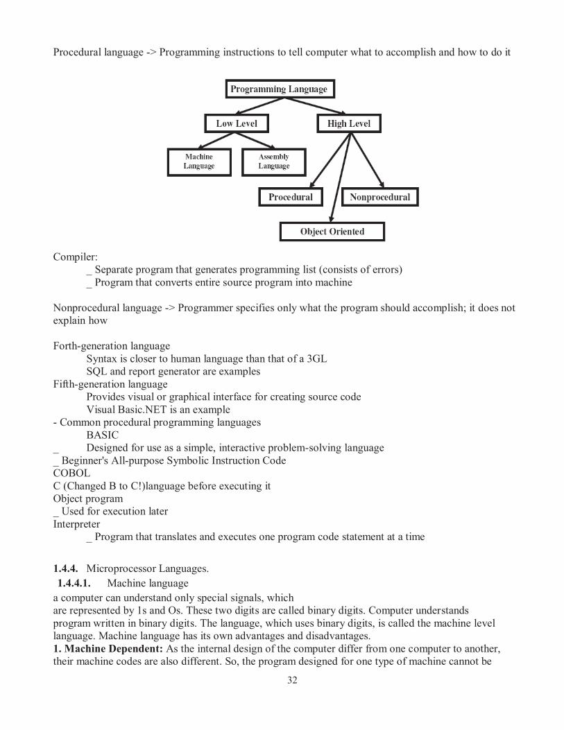
- Two basic types: Low- and high-level programming languages Low-level: Programming language that is machine-dependent _ Must be run on specific machines High-level: Language that is machine-independent _ Can be run on different types of machines
1.4.3. Categories of programming languages
Machine language Only language computer understands directly
Assembly language Instructions made up of symbolic instruction codes Assembler converts the source code to the machine language
Third-generation language Uses a series of English-like words to write instructions
32
Procedural language -> Programming instructions to tell computer what to accomplish and how to do it
Compiler:
_ Separate program that generates programming list (consists of errors) _ Program that converts entire source program into machine
Nonprocedural language -> Programmer specifies only what the program should accomplish; it does not explain how Forth-generation language
Syntax is closer to human language than that of a 3GL SQL and report generator are examples
Fifth-generation language Provides visual or graphical interface for creating source code Visual Basic.NET is an example - Common procedural programming languages
BASIC _ Designed for use as a simple, interactive problem-solving language _ Beginner's All-purpose Symbolic Instruction Code COBOL C (Changed B to C!)language before executing it Object program _ Used for execution later Interpreter
_ Program that translates and executes one program code statement at a time
1.4.4. Microprocessor Languages.
1.4.4.1. Machine language
a computer can understand only special signals, which are represented by 1s and Os. These two digits are called binary digits. Computer understands program written in binary digits. The language, which uses binary digits, is called the machine level language. Machine language has its own advantages and disadvantages. 1. Machine Dependent: As the internal design of the computer differ from one computer to another, their machine codes are also different. So, the program designed for one type of machine cannot be
33
used for another type of machine. 2. Fast processing: As the machine code instructions are directly understood by the computer and do not require any translator, the program written in the machine language are very fast and processed very quickly. 3. Error prone: As the programmer has to write all the instructions using 0's and 1's it is a very cumbersome job, the chances of error prone codes are more in writing a machine level language program. 4. Difficult to use: As machine language uses only 0 and 1 two symbols to represent all data and instructions it is very difficult to remember the machine codes for the different commands.
1.4.4.2. Assembly language
Even the incredibly simple microprocessor will have a fairly large set of instructions that it can perform. The collection of instructions is implemented as bit patterns, each one of which has a different meaning when loaded into the instruction register. Humans are not particularly good at remembering bit patterns, so a set of short words are defined to represent the different bit patterns. This collection of words is called the assembly language of the processor. An assembler can translate the words into their bit patterns very easily, and then the output of the assembler is placed in memory for the microprocessor to execute. An opcode (operation code) is the portion of a machine language instruction that specifies the operation to be performed. Their specification and format are laid out in the instruction set architecture of the processor in question (which may be a general CPU or a more specialized processing unit). Apart from the opcode itself, an instruction normally also has one or more specifiers for operands (i.e. data) on which the operation should act, although some operations may have implicit operands, or none at all. Assembly language, or just assembly, is a low-level programming language, which uses mnemonics, instructions and operands to represent machine code. This enhances the readability while still giving precise control over the machine instructions. 1.4.4.3. High level languages
PROGRAM TRANSLATORS
Since a computer can only understand machine language, any program written in a High level language such as Visual Basic, cannot be executed directly; therefore, it must be first translated to machine language. In order to convert it to machine language a translator is required. There are 3 types of translators used for translating a program written in High level language or assembly language to a form that the computer can execute (i.e., machine code). The three types of translators are: 1. Assembler
Assembly language is a low-level programming language in which a mnemonic is used to represent each of the machine language instructions. Assembly languages were developed to make programming easy. Since the computer cannot understand assembly language, however, a program called assembler is used to convert assembly language programs into machine code 2. Compiler
The high-level languages are English-like and easy to learn and program. A Compiler is a program that translates a high level language into machine code. The Visual Basic compiler, for example, translates a program written in Pascal into machine code that can be run on a PC.
34
Advantages of a Compiler
1. Fast in execution. 2. The object/executable code produced by a compiler can be distributed or executed without having to have the compiler present. 3. The object program can be used whenever required without the need to of recompilation. Disadvantages of a Compiler
1. Debugging (Correcting errors) a program is much harder. Therefore, not so good at finding errors. 2. When an error is found, the whole program has to be re-compiled.
3. Interpreter
An Interpreter is also a program that translates high-level source code into executable code. However, the difference between a compiler and an interpreter is that an interpreter translates one line at a time and then executes it, no object code is produced and so the program has to be interpreted each time, it is to be run. If the program performs a section code 1000 times, then the section is translated into machine code 1000 times since each line is interpreted and then executed. Advantages
1. Good at locating errors in programs 2. Debugging is easier since the interpreter stops when it encounters an error. 3. Useful for learning purpose. Note: Debugging is the process of finding and removing errors from a program. Disadvantages
1. Rather slow. 2. No object code is produced, so a translation has to be done every time the program is running. 3. For the program to run, the Interpreter must be present.
1.5. DATA TRANSFER
Data exchange or transfers which occur between a peripheral device and the μC fall into one of the following two broad categories: 1.5.1. Programmed Data Transfer
A software routine residing in memory requests the peripheral device for data transfer to or from the μP.
Generally, the data is transferred to or from the accumulator though in some μPs, others internal registers
may also participate in the transfer. Programmed data transfers are generally used when a small amount of data is transferred with relatively slow I/O devices, e.g., A/D and D/A converters, peripheral multiplier, peripheral floating point arithmetic unit etc. In these cases, usually one word of data is transferred at a time. 1.5.2. Direct Memory Access (DMA) Transfer or Cycle Stealing Transfer
In this mode, the data transfer is controlled by the peripheral device. The μP is forced to hold on by an I/O device until the data transfer between the device and the memory is complete. Since the data control transfer is controlled entirely by hardware, the interface is more complex than that required for a programmed data transfer. DMA transfer is used when a large block of data is to be transferred, for example, for transferring data from peripheral mass storage devices like the floppy disk and high-speed card reader.
1.6. Microprocessors vs microcontrollers Microprocessors: op
high performance, general purpose “brains” for PCs and workstations Instruction decode and control, arithmetic/logic operations, registers, timing, external control
Microcontrollers:
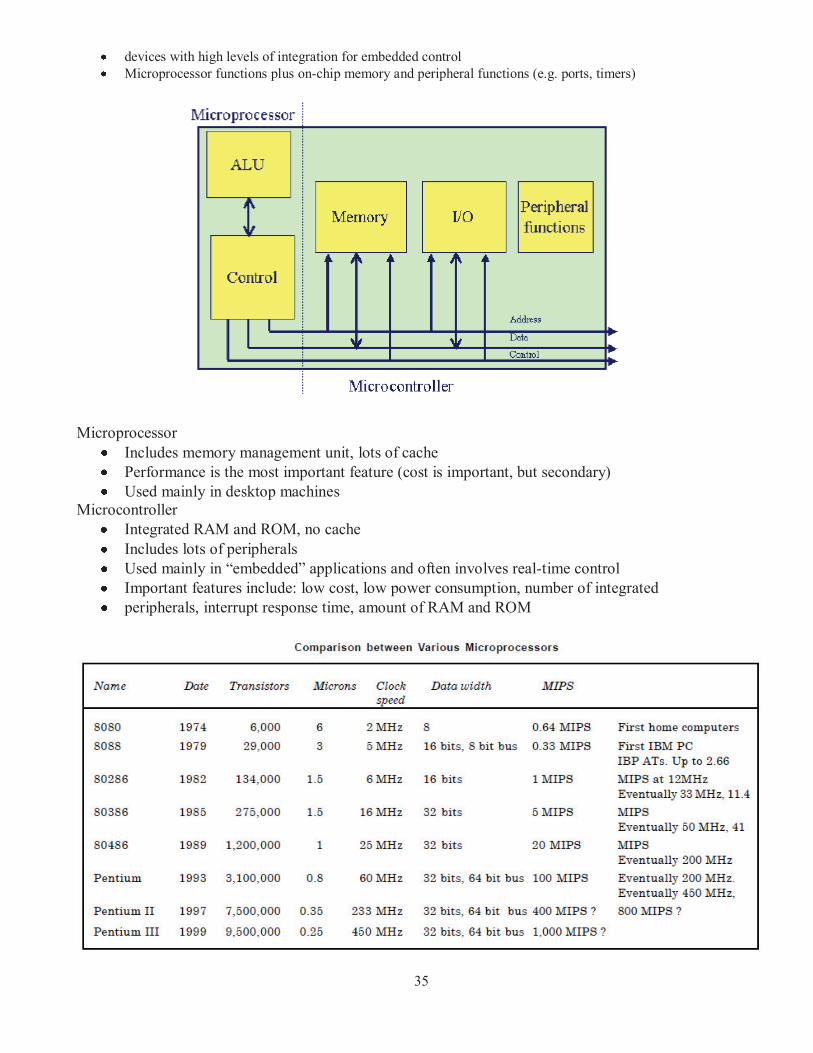
35
devices with high levels of integration for embedded control Microprocessor functions plus on-chip memory and peripheral functions (e.g. ports, timers)
Microprocessor Includes memory management unit, lots of cache Performance is the most important feature (cost is important, but secondary) Used mainly in desktop machines
Microcontroller Integrated RAM and ROM, no cache Includes lots of peripherals Used mainly in “embedded” applications and often involves real-time control Important features include: low cost, low power consumption, number of integrated peripherals, interrupt response time, amount of RAM and ROM
36
1.7. ARCHITECTURAL ADVANCEMENT
The first microprocessor was announced in 1971 by Intel Corporation, U.S.A. This was the Intel 4004. It was on a single chip and was a 4-bit microprocessor (i.e., operated on 4 bits of data at a time).
Encouraged by the success of 4004, Intel Corp. introduced its enhanced version, the Intel 4040. Many other companies also announced 4-bit microprocessors, examples are Rockwell International’s PPS4,
NEC’s μCOM 4 and Toshiba’s T3472. The first 8-bit microprocessor was announced in 1973, again by Intel Corp. This was the Intel
8008. An improved version, Intel 8030, followed. Several other companies followed the suit. Today the batter known 8-bit mPs are Intel’s 8085, Motorola’s M6800, NEC’s μCOM85AF, National * SC/MP, Zilog Corporation’s Z80 and Fairchild’s F8.
Then followed 12-bit and 16-bit μPs. Examples of 12-bit μPs are Intersil’s IM 6100 and Toshiba’s
T3190 and those of 16-bit μPs Intel’s 8086, Fairchild’s 9440, Texas Instrument’s TMS 9940 and TMS
9980, Zilog’s Z8000, Motorola’s M68000. The developments in μP since 1971 have been in the direction of (a) improving architecture, (b) improving instruction set, (c) increasing speeds, (d) simplifying power requirements and (e) incorporating more and more memory space and I/O facilities in the same chip (thus giving use
to single chip computers).
• The date is the year that the processor was first introduced. Many processors are reintroduced at higher clock speeds for many years after the original release date. • Transistors is the number of transistors on the chip. You can see that the number of transistors on a single chip has risen steadily over the years. • Microns is the width, in microns, of the smallest wire on the chip. For comparison, a human hair is 100 microns thick. As the feature size on the chip goes down, the number of transistors rises. Clock speed is the maximum rate that the chip can be clocked. Clock speed will make more sense in the next section. • Data Width is the width of the ALU. An 8-bit ALU can add/subtract/multiply/etc. two 8-bit numbers, while a 32-bit ALU can manipulate 32-bit numbers. An 8-bit ALU would have to execute 4 instructions to add two 32- bit numbers, while a 32-bit ALU can do it in one instruction. In many cases the external data bus is the same width as the ALU, but not always. The 8088 had a 16-bit ALU and an 8-bit bus, while the modern Pentiums fetch data 64 bits at a time for their 32-bit ALUs. • MIPS stands for Millions of Instructions Per Second, and is a rough measure of the performance of a CPU. Modern CPUs can do so many different things that MIPS ratings lose a lot of their meaning, but you can get a general sense of the relative power of the CPUs from this column.
In general, there is a relationship between clock speed and MIPS. The maximum clock speed is a function of the manufacturing process and delays within the chip. There is also a relationship between the number of transistors and MIPS. For example, the 8088 clocked at 5 MHz but only executed at 0.33 MIPS (about 1 instruction per 15 clock cycles). Modern processors can often execute at a rate of 2 instructions per clock cycle. That improvement is directly related to the number of transistors on the chip.
1.7.1. Key Architectural Trends
• Increase performance at 1.6x per year (2X/1.5yr)
– True from 1985-present • Combination of technology and architectural enhancements
37
– Technology provides faster transistors ( 1/lithographic feature size) and more of them
– Faster transistors leads to high clock rates
– More transistors (“Moore’s Law”):
• Architectural ideas turn transistors into performance
– Responsible for about half the yearly performance growth • Two key architectural directions
– Sophisticated memory hierarchies
– Exploiting instruction level parallelism
Memory Hierarchies • Caches: hide latency of DRAM and increase BW
– CPU-DRAM access gap has grown by a factor of 30-50! • Trend 1: Increasingly large caches
– On-chip: from 128 bytes (1984) to 100,000+ bytes
– Multilevel caches: add another level of caching
• First multilevel cache:1986
• Secondary cache sizes today: 128,000 B to 16,000,000 B
• Third level caches: 1998 • Trend 2: Advances in caching techniques:
– Reduce or hide cache miss latencies
• early restart after cache miss (1992)
• nonblocking caches: continue during a cache miss (1994)
– Cache aware combos: computers, compilers, code writers • prefetching: instruction to bring data into cache early
Exploiting Instruction Level Parallelism (ILP)
• ILP is the implicit parallelism among instructions (programmer not aware)
• Exploited by
– Overlapping execution in a pipeline
– Issuing multiple instruction per clock• superscalar: uses dynamic issue decision (HW driven)
• VLIW: uses static issue decision (SW driven)
• 1985: simple microprocessor pipeline (1 instr/clock)
• 1990: first static multiple issue microprocessors
• 1995: sophisticated dynamic schemes
– determine parallelism dynamically – execute instructions out-of-order
– speculative execution depending on branch prediction
• “Off-the-shelf” ILP techniques yielded 15 year path of 2X performance every 1.5 years => 1000X faster!
ClusterOnaChip (CoC) • Use several simple processors on a single chip:
– Performance goes up linearly in number of transistors
– Simpler processors can run at faster clocks
– Less design cost/time, Less time to market risk (reuse)
38
• Inspiration: Google
– Search engine for world: 100M/day
– Economical, scalable build block: PC cluster today 8000 PCs, 16000 disks
– Advantages in fault tolerance, scalability, cost/performance
• 32-bit MPU as the new “Transistor”
– “Cluster on a chip” with 1000s of processors enable amazing MIPS/$, MIPS/watt for cluster applications
– MPUs combined with dense memory + system on a chip CAD
• 30 years ago Intel 4004 used 2300 transistors: when 2300 32-bit RISC processors on a single chip?
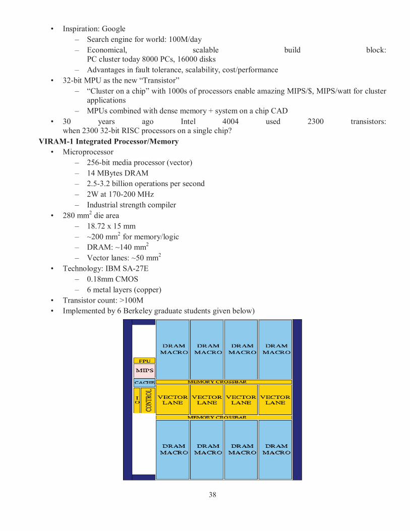
VIRAM-1 Integrated Processor/Memory
• Microprocessor
– 256-bit media processor (vector)
– 14 MBytes DRAM – 2.5-3.2 billion operations per second
– 2W at 170-200 MHz
– Industrial strength compiler
• 280 mm2 die area
– 18.72 x 15 mm
– ~200 mm2 for memory/logic – DRAM: ~140 mm2
– Vector lanes: ~50 mm2
• Technology: IBM SA-27E
– 0.18mm CMOS
– 6 metal layers (copper)
• Transistor count: >100M • Implemented by 6 Berkeley graduate students given below)
39
1.7.2. Family of Microprocessors
1978: 8086 (16 bit architecture) • 1980: 8087
• Floating point coprocessor is added • 1982: 80286
• Increases address space to 24 bits • 1985: 80386:
• 32 bits Add, • Virtual Mem & new add modes • Protected mode (OS support) • 1989-95: 80486/Pentium/Pro • Added a few instructions of base MMX
1997: Pentium II
• 57 new “MMX” instructions are added, • 1999: Pentium III:
• Out of Order, added another 70 Streaming SIMD Ext (SSE) • 2001: Pentium 4
• Net burst, another 144 instructions (SSE2) • 2003: PI4 HT, Trace Cache • 2005: Centrino, low power • 2007: Core architecture, Duo • 2008: Atom, Quad core with HT…. • 2009---:Multi core (Large chip multiprocessor) 2010 core i3 2011 core i5 Core i7…………….towards smaller technology(self check)Reference Wikipedia 1.7.3. MANUFACTURING TECHNOLOGIES
Broadly two technologies have been used in the manufacturer of μPs: MOS and Bipolar. The
majority of μPs available in the market use MOS technology because of its two distinct merits, namely, a
higher component density and a lower manufacturing cost. The bipolar-technologybased μPs are limited to
special applications that call for high speeds in which respect MOS devices are inferior. Because of the size problem the bipolar μPs are usually made in bit-slice configuration; examples being Intel’s 3002 (2-bit slice, TTL), Transitron’s 1601 (4-bit slice, TTL) and Texas Instrument’s SBP 0400 (4-bit slice, TIL).
The first few types of μPs to be announced (e.g., 4004, 4040, 8008) were based on PMOS
technology, which is now obsolete for μPs because of its speed limitation. The NMOS is the main
technology today in use for low cost μPs (e.g., 8080, 8085, Z-80, 6800 808, 6800, 8086, Z-8000, 68000). The CMOS technology based μPs (e.g., RCA’s COSMAC) have limited application because of lower
packing density and higher cost. The exceptions are the less cost-sensitive military and aerospace applications, where low power dissipation (typical of the CMOS devices) is of prime importance.
1.8. SUMMARY
The various concepts and terms discussed in this chapter are summarized below:
40
1.8.1. Computer Structure
· Digital Computer-a programmable machine that processes binary data. It includes four components: CPU (ALU plus control unit), memory, input, and output.
· CPU-the Central Processing Unit. The group of circuits that processes data and provides control signals and timing. It includes the arithmetic/logic unit, registers, instruction decoder, and the control unit.
· ALU-the group of circuits that performs arithmetic and logic operations. The ALU is a part of the CPU.
· Control Unit-The group of circuits that provides timing and signals to all operations in the computer and controls data flow.
· Memory-a medium that stores binary information (instructions and data).
· Input -a device that transfers information from the outside world to the computer.
· Output-a device that transfers information from the computer to the outside world.
1.8.2. Microprocessor-Based Systems
· Microprocessor-a semiconductor device (integrated circuit) that is manufactured by using the large-scale integration technique. It includes the ALU, register arrays, and control circuits on a single chip.
· Microcomputer-a computer that uses a microprocessor as its CPU. It includes four components: microprocessor, memory, input, and output.
· Bus---a group of lines used to transfer bits between the microprocessor and other components of the computer system.
· ROM-Read-Only Memory. A memory that stores binary information permanently. The information can be read from this memory but cannot be altered.
· R/WM-Read/Write Memory. A memory that stores binary information during the operation of the computer. This memory is used as a writing pad to write user programs and data. The information stored in this memory can be easily read and altered.
1.8.3. Computer Languages
· · Machine Language-the binary medium of communication with a computer through a designed set of instructions specific to each computer.
41
· Assembly Language-a medium of communication with a computer in which programs are written in mnemonics. An assembly language is specific to a given computer.
· Low-Level Language-a medium of communication that is machine-dependent, or specific to a given computer. The machine and the assembly languages of a computer are considered low-level languages. Programs written in these languages are not transferable to different types of machines.
· High-Level Language-a medium of communication independent of a given computer. Programs are written in English-like words, and they can be executed on a machine using a translator (a compiler or an interpreter).
· Compiler-a program that translates English-like words of a 'high-level language into the machine language of a computer. A compiler reads a given program, called a source code, in its entirety, and then translates the program into the machine language, which is called an object code.
· Interpreter-a program that translates the English-like statements of a high level language into the machine language of a computer. An interpreter translates one statement at a time from a source code to an object code.
· Assembler-a computer program that translates an assembly language program from mnemonics to the binary machine code of a computer.
42
CHAPTER 2
INTRODUCTION TO
16-BIT MICROPROCESSOR
43
2.1. INTRODUCTION
Overview or features of 8086
It is a 16-bit Microprocessor (μp).It’s ALU, internal registers works with 16bit binary word. 8086 has a 20 bit address bus can access up to 220= 1 MB memory locations. 8086 has a 16bit data bus. It can read or write data to a memory/port either 16bits or 8 bit at a time. It can support up to 64K I/O ports. It provides 14, 16 -bit registers. Frequency range of 8086 is 6-10 MHz It has multiplexed address and data bus AD0- AD15 and A16 – A19. It requires single phase clock with 33% duty cycle to provide internal timing. It can prefetch upto 6 instruction bytes from memory and queues them in order to speed up
instruction execution. It requires +5V power supply. A 40 pin dual in line package. 8086 is designed to operate in two modes, Minimum mode and Maximum mode.
o The minimum mode is selected by applying logic 1 to the MN / MX# input pin. This is a single microprocessor configuration.
o The maximum mode is selected by applying logic 0 to the MN / MX# input pin. This is a multi micro processors configuration.
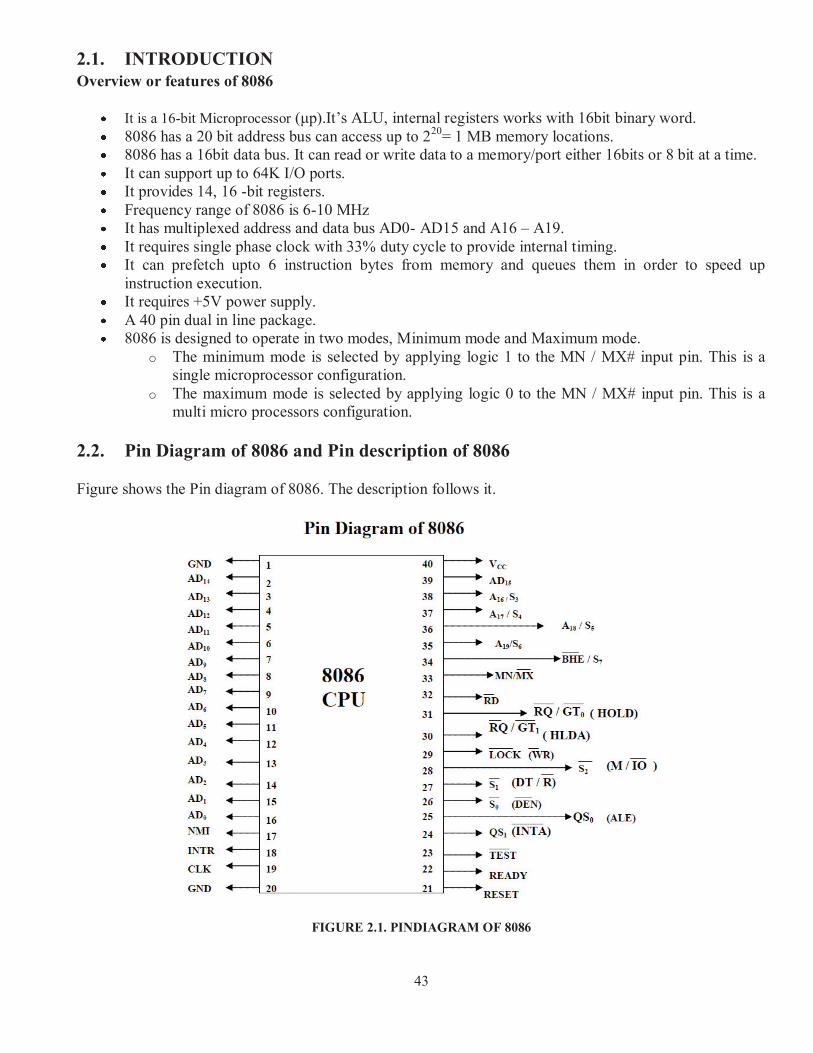
2.2. Pin Diagram of 8086 and Pin description of 8086
Figure shows the Pin diagram of 8086. The description follows it.
FIGURE 2.1. PINDIAGRAM OF 8086
44
The Microprocessor 8086 is a 16-bit CPU available in different clock rates and packaged in a 40 pin CERDIP or plastic package.
The 8086 operates in single processor or multiprocessor configuration to achieve high performance. The pins serve a particular function in minimum mode (single processor mode) and other function in maximum mode configuration (multiprocessor mode).
The 8086 signals can be categorized in three groups. o The first are the signal having common functions in minimum as well as maximum mode. o The second are the signals which have special functions for minimum mode o The third are the signals having special functions for maximum mode.
The following signal descriptions are common for both modes. AD15-AD0: These are the time multiplexed memory I/O address and data lines.
o Address remains on the lines during T1 state, while the data is available on the data bus during T2, T3 and T4. These lines are active high and float to a tristate during interrupt acknowledge and local bus hold acknowledge cycles.
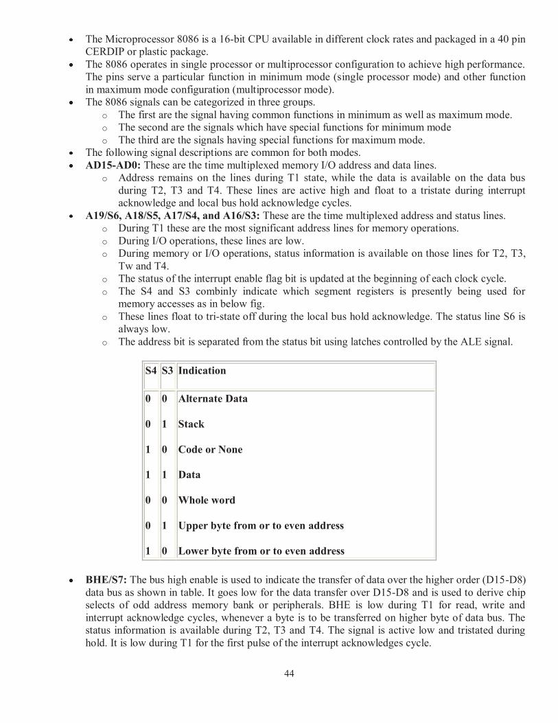
A19/S6, A18/S5, A17/S4, and A16/S3: These are the time multiplexed address and status lines. o During T1 these are the most significant address lines for memory operations. o During I/O operations, these lines are low. o During memory or I/O operations, status information is available on those lines for T2, T3,
Tw and T4. o The status of the interrupt enable flag bit is updated at the beginning of each clock cycle. o The S4 and S3 combinly indicate which segment registers is presently being used for
memory accesses as in below fig. o These lines float to tri-state off during the local bus hold acknowledge. The status line S6 is
always low. o The address bit is separated from the status bit using latches controlled by the ALE signal.
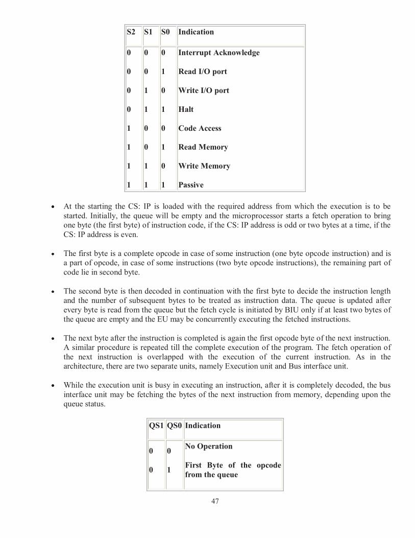
S4 S3 Indication
0
0
1
1
0
0
1
0
1
0
1
0
1
0
Alternate Data
Stack
Code or None
Data
Whole word
Upper byte from or to even address
Lower byte from or to even address
BHE/S7: The bus high enable is used to indicate the transfer of data over the higher order (D15-D8) data bus as shown in table. It goes low for the data transfer over D15-D8 and is used to derive chip selects of odd address memory bank or peripherals. BHE is low during T1 for read, write and interrupt acknowledge cycles, whenever a byte is to be transferred on higher byte of data bus. The status information is available during T2, T3 and T4. The signal is active low and tristated during hold. It is low during T1 for the first pulse of the interrupt acknowledges cycle.
45
RD – Read: This signal on low indicates the peripheral that the processor is performing memory or I/O read operation. RD is active low and shows the state for T2, T3, and Tw of any read cycle. The signal remains tristated during the hold acknowledge.
READY: This is the acknowledgement from the slow device or memory that they have completed the data transfer. The signal made available by the devices is synchronized by the 8284A clock generator to provide ready input to the 8086. The signal is active high.
INTR-Interrupt Request: This is a triggered input. This is sampled during the last clock cycles of each instruction to determine the availability of the request. If any interrupt request is pending, the processor enters the interrupt acknowledge cycle. This can be internally masked by resulting the interrupt enable flag. This signal is active high and internally synchronized.
TEST: This input is examined by a ‘WAIT’ instruction. If the TEST pin goes low, execution will
continue, else the processor remains in an idle state. The input is synchronized internally during each clock cycle on leading edge of clock.
CLK- Clock Input: The clock input provides the basic timing for processor operation and bus control activity. It’s an asymmetric square wave with 33% duty cycle.
2.2.1. Pin description of 8086
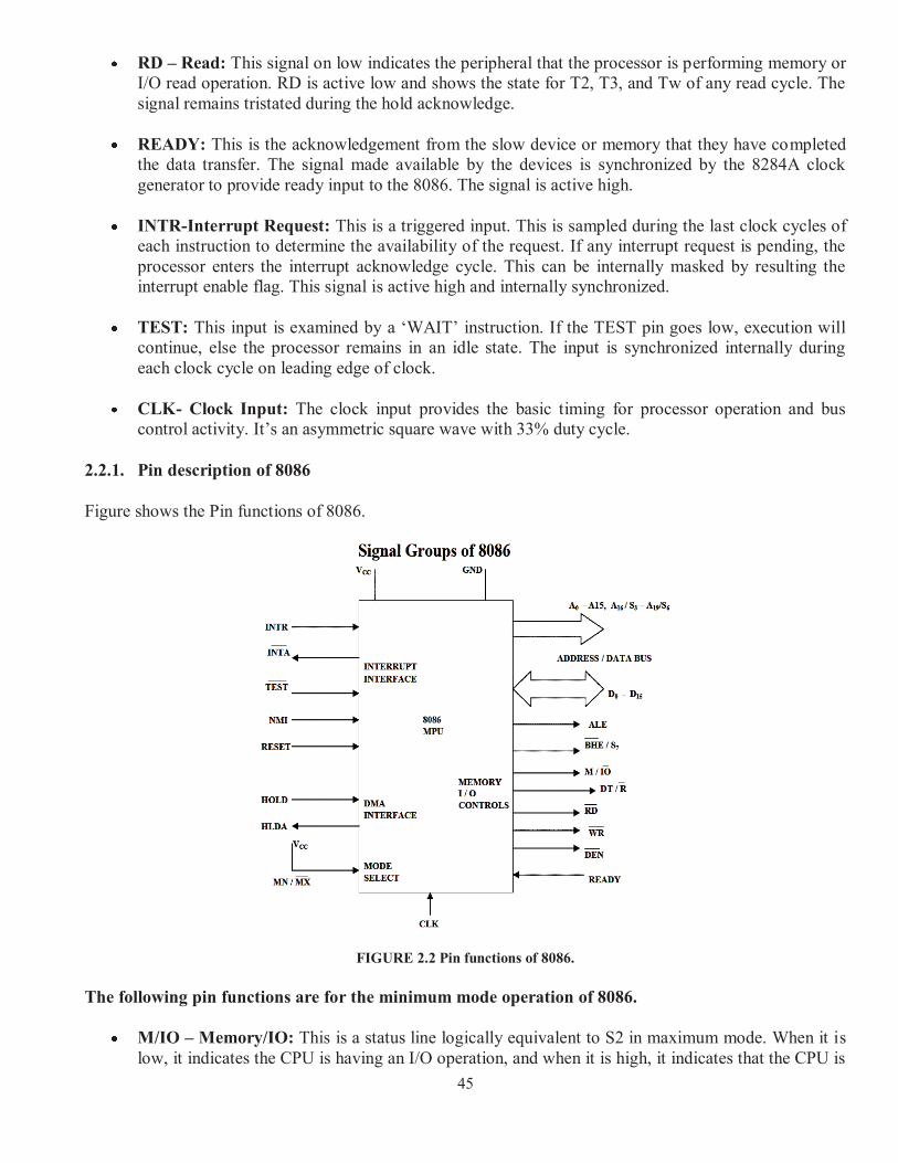
Figure shows the Pin functions of 8086.
FIGURE 2.2 Pin functions of 8086.
The following pin functions are for the minimum mode operation of 8086.
M/IO – Memory/IO: This is a status line logically equivalent to S2 in maximum mode. When it is low, it indicates the CPU is having an I/O operation, and when it is high, it indicates that the CPU is
46
having a memory operation. This line becomes active high in the previous T4 and remains active till final T4 of the current cycle. It is tristated during local bus “hold acknowledge “.
INTA – Interrupt Acknowledge: This signal is used as a read strobe for interrupt acknowledge cycles. i.e. when it goes low, the processor has accepted the interrupt.
ALE – Address Latch Enable: This output signal indicates the availability of the valid address on the address/data lines, and is connected to latch enable input of latches. This signal is active high and is never tristated.
DT/R – Data Transmit/Receive: This output is used to decide the direction of data flow through the transreceivers (bidirectional buffers). When the processor sends out data, this signal is high and when the processor is receiving data, this signal is low.
DEN – Data Enable: This signal indicates the availability of valid data over the address/data lines. It is used to enable the transreceivers (bidirectional buffers) to separate the data from the multiplexed address/data signal. It is active from the middle of T2 until the middle of T4. This is tristated during ‘hold acknowledge’ cycle.
HOLD, HLDA- Acknowledge: When the HOLD line goes high, it indicates to the processor that another master is requesting the bus access. The processor, after receiving the HOLD request, issues the hold acknowledge signal on HLDA pin, in the middle of the next clock cycle after completing the current bus cycle.
At the same time, the processor floats the local bus and control lines. When the processor detects the HOLD line low, it lowers the HLDA signal. HOLD is an asynchronous input, and is should be externally synchronized. If the DMA request is made while the CPU is performing a memory or I/O cycle, it will release the local bus during T4 provided :
1. The request occurs on or before T2 state of the current cycle. 2. The current cycle is not operating over the lower byte of a word. 3. The current cycle is not the first acknowledge of an interrupt acknowledge sequence. 4. A Lock instruction is not being executed.
The following pin functions are applicable for maximum mode operation of 8086.
S2, S1, and S0 – Status Lines: These are the status lines which reflect the type of operation, being carried out by the processor. These become activity during T4 of the previous cycle and active during T1 and T2 of the current bus cycles.
LOCK: This output pin indicates that other system bus master will be prevented from gaining the system bus, while the LOCK signal is low. The LOCK signal is activated by the ‘LOCK’ prefix
instruction and remains active until the completion of the next instruction. When the CPU is executing a critical instruction which requires the system bus, the LOCK prefix instruction ensures that other processors connected in the system will not gain the control of the bus.
The 8086, while executing the prefixed instruction, asserts the bus lock signal output, which may be connected to an external bus controller. By prefetching the instruction, there is a considerable speeding up in instruction execution in 8086. This is known as instruction pipelining.
47
S2 S1 S0 Indication
0
0
0
0
1
1
1
1
0
0
1
1
0
0
1
1
0
1
0
1
0
1
0
1
Interrupt Acknowledge
Read I/O port
Write I/O port
Halt
Code Access
Read Memory
Write Memory
Passive
At the starting the CS: IP is loaded with the required address from which the execution is to be started. Initially, the queue will be empty and the microprocessor starts a fetch operation to bring one byte (the first byte) of instruction code, if the CS: IP address is odd or two bytes at a time, if the CS: IP address is even.
The first byte is a complete opcode in case of some instruction (one byte opcode instruction) and is a part of opcode, in case of some instructions (two byte opcode instructions), the remaining part of code lie in second byte.
The second byte is then decoded in continuation with the first byte to decide the instruction length and the number of subsequent bytes to be treated as instruction data. The queue is updated after every byte is read from the queue but the fetch cycle is initiated by BIU only if at least two bytes of the queue are empty and the EU may be concurrently executing the fetched instructions.
The next byte after the instruction is completed is again the first opcode byte of the next instruction. A similar procedure is repeated till the complete execution of the program. The fetch operation of the next instruction is overlapped with the execution of the current instruction. As in the architecture, there are two separate units, namely Execution unit and Bus interface unit.
While the execution unit is busy in executing an instruction, after it is completely decoded, the bus interface unit may be fetching the bytes of the next instruction from memory, depending upon the queue status.
QS1 QS0 Indication
0
0
0
1
No Operation
First Byte of the opcode
from the queue
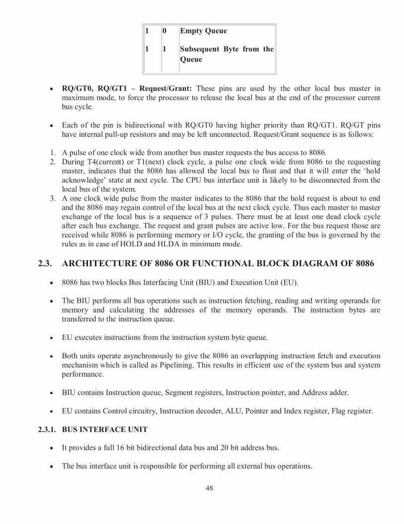
48
1
1
0
1
Empty Queue
Subsequent Byte from the
Queue
RQ/GT0, RQ/GT1 – Request/Grant: These pins are used by the other local bus master in maximum mode, to force the processor to release the local bus at the end of the processor current bus cycle.
Each of the pin is bidirectional with RQ/GT0 having higher priority than RQ/GT1. RQ/GT pins have internal pull-up resistors and may be left unconnected. Request/Grant sequence is as follows:
1. A pulse of one clock wide from another bus master requests the bus access to 8086. 2. During T4(current) or T1(next) clock cycle, a pulse one clock wide from 8086 to the requesting
master, indicates that the 8086 has allowed the local bus to float and that it will enter the ‘hold
acknowledge’ state at next cycle. The CPU bus interface unit is likely to be disconnected from the
local bus of the system. 3. A one clock wide pulse from the master indicates to the 8086 that the hold request is about to end
and the 8086 may regain control of the local bus at the next clock cycle. Thus each master to master exchange of the local bus is a sequence of 3 pulses. There must be at least one dead clock cycle after each bus exchange. The request and grant pulses are active low. For the bus request those are received while 8086 is performing memory or I/O cycle, the granting of the bus is governed by the rules as in case of HOLD and HLDA in minimum mode.
2.3. ARCHITECTURE OF 8086 OR FUNCTIONAL BLOCK DIAGRAM OF 8086
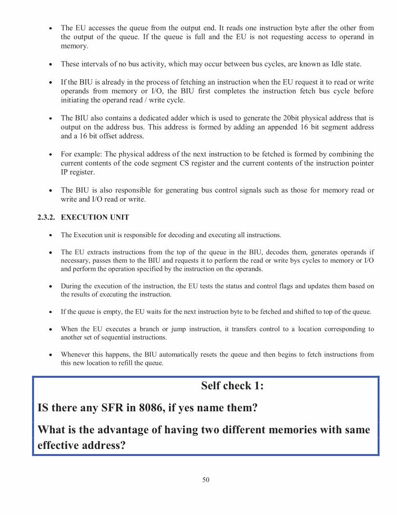
8086 has two blocks Bus Interfacing Unit (BIU) and Execution Unit (EU).
The BIU performs all bus operations such as instruction fetching, reading and writing operands for memory and calculating the addresses of the memory operands. The instruction bytes are transferred to the instruction queue.
EU executes instructions from the instruction system byte queue.
Both units operate asynchronously to give the 8086 an overlapping instruction fetch and execution mechanism which is called as Pipelining. This results in efficient use of the system bus and system performance.
BIU contains Instruction queue, Segment registers, Instruction pointer, and Address adder.
EU contains Control circuitry, Instruction decoder, ALU, Pointer and Index register, Flag register.
2.3.1. BUS INTERFACE UNIT
It provides a full 16 bit bidirectional data bus and 20 bit address bus.
The bus interface unit is responsible for performing all external bus operations.
49
Specifically it has the following functions:
Instruction fetches Instruction queuing, Operand fetch and storage, Address relocation and Bus control.
The BIU uses a mechanism known as an instruction stream queue to implement pipeline
architecture.
This queue permits prefetch of up to six bytes of instruction code. When ever the queue of the BIU is not full, it has room for at least two more bytes and at the same time the EU is not requesting it to read or write operands from memory, the BIU is free to look ahead in the program by prefetching the next sequential instruction.
FIGURE 2.3 Block diagram of 8086.
These prefetching instructions are held in its FIFO queue. With its 16 bit data bus, the BIU fetches two instruction bytes in a single memory cycle.
After a byte is loaded at the input end of the queue, it automatically shifts up through the FIFO to the empty location nearest the output.
50
The EU accesses the queue from the output end. It reads one instruction byte after the other from the output of the queue. If the queue is full and the EU is not requesting access to operand in memory.
These intervals of no bus activity, which may occur between bus cycles, are known as Idle state.
If the BIU is already in the process of fetching an instruction when the EU request it to read or write operands from memory or I/O, the BIU first completes the instruction fetch bus cycle before initiating the operand read / write cycle.
The BIU also contains a dedicated adder which is used to generate the 20bit physical address that is output on the address bus. This address is formed by adding an appended 16 bit segment address and a 16 bit offset address.
For example: The physical address of the next instruction to be fetched is formed by combining the current contents of the code segment CS register and the current contents of the instruction pointer IP register.
The BIU is also responsible for generating bus control signals such as those for memory read or write and I/O read or write.
2.3.2. EXECUTION UNIT
The Execution unit is responsible for decoding and executing all instructions.
The EU extracts instructions from the top of the queue in the BIU, decodes them, generates operands if necessary, passes them to the BIU and requests it to perform the read or write bys cycles to memory or I/O and perform the operation specified by the instruction on the operands.
During the execution of the instruction, the EU tests the status and control flags and updates them based on the results of executing the instruction.
If the queue is empty, the EU waits for the next instruction byte to be fetched and shifted to top of the queue.
When the EU executes a branch or jump instruction, it transfers control to a location corresponding to another set of sequential instructions.
Whenever this happens, the BIU automatically resets the queue and then begins to fetch instructions from this new location to refill the queue.
Self check 1:
IS there any SFR in 8086, if yes name them?
What is the advantage of having two different memories with same
effective address?
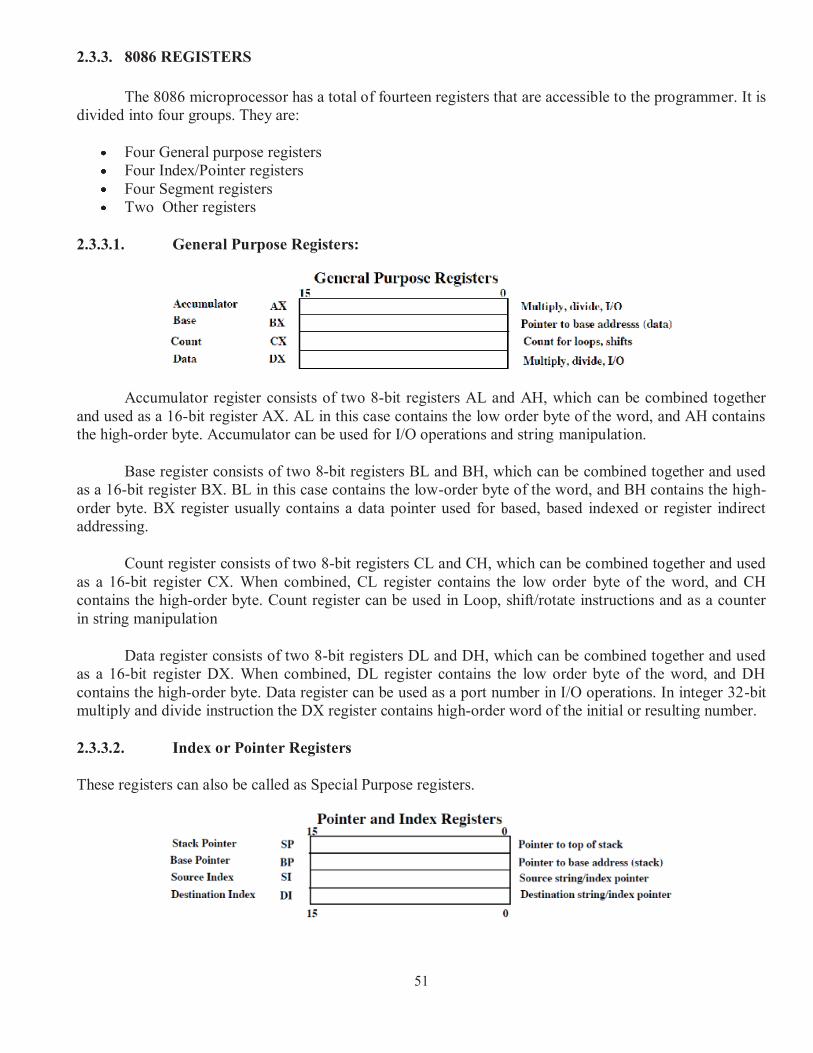
51
2.3.3. 8086 REGISTERS
The 8086 microprocessor has a total of fourteen registers that are accessible to the programmer. It is divided into four groups. They are:
Four General purpose registers Four Index/Pointer registers Four Segment registers Two Other registers
2.3.3.1. General Purpose Registers:
Accumulator register consists of two 8-bit registers AL and AH, which can be combined together and used as a 16-bit register AX. AL in this case contains the low order byte of the word, and AH contains the high-order byte. Accumulator can be used for I/O operations and string manipulation.
Base register consists of two 8-bit registers BL and BH, which can be combined together and used as a 16-bit register BX. BL in this case contains the low-order byte of the word, and BH contains the high-order byte. BX register usually contains a data pointer used for based, based indexed or register indirect addressing.
Count register consists of two 8-bit registers CL and CH, which can be combined together and used as a 16-bit register CX. When combined, CL register contains the low order byte of the word, and CH contains the high-order byte. Count register can be used in Loop, shift/rotate instructions and as a counter in string manipulation
Data register consists of two 8-bit registers DL and DH, which can be combined together and used as a 16-bit register DX. When combined, DL register contains the low order byte of the word, and DH contains the high-order byte. Data register can be used as a port number in I/O operations. In integer 32-bit multiply and divide instruction the DX register contains high-order word of the initial or resulting number.
2.3.3.2. Index or Pointer Registers
These registers can also be called as Special Purpose registers.
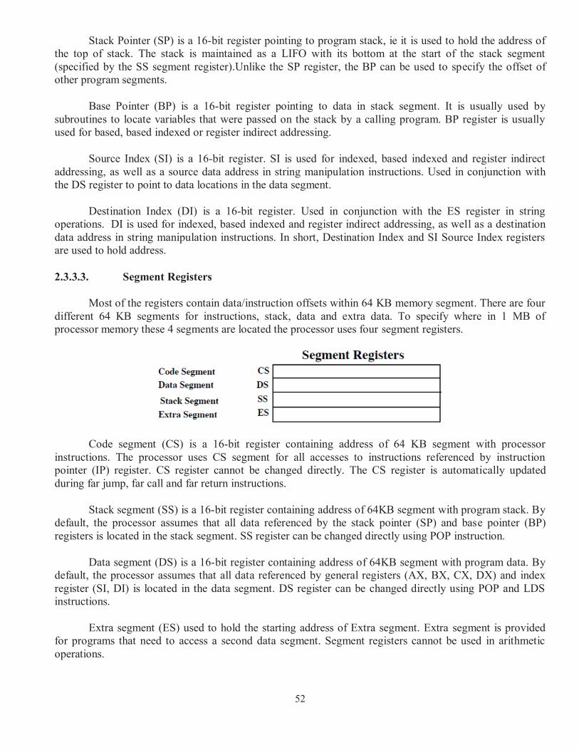
52
Stack Pointer (SP) is a 16-bit register pointing to program stack, ie it is used to hold the address of the top of stack. The stack is maintained as a LIFO with its bottom at the start of the stack segment (specified by the SS segment register).Unlike the SP register, the BP can be used to specify the offset of other program segments.
Base Pointer (BP) is a 16-bit register pointing to data in stack segment. It is usually used by subroutines to locate variables that were passed on the stack by a calling program. BP register is usually used for based, based indexed or register indirect addressing.
Source Index (SI) is a 16-bit register. SI is used for indexed, based indexed and register indirect addressing, as well as a source data address in string manipulation instructions. Used in conjunction with the DS register to point to data locations in the data segment.
Destination Index (DI) is a 16-bit register. Used in conjunction with the ES register in string operations. DI is used for indexed, based indexed and register indirect addressing, as well as a destination data address in string manipulation instructions. In short, Destination Index and SI Source Index registers are used to hold address.
2.3.3.3. Segment Registers
Most of the registers contain data/instruction offsets within 64 KB memory segment. There are four different 64 KB segments for instructions, stack, data and extra data. To specify where in 1 MB of processor memory these 4 segments are located the processor uses four segment registers.
Code segment (CS) is a 16-bit register containing address of 64 KB segment with processor instructions. The processor uses CS segment for all accesses to instructions referenced by instruction pointer (IP) register. CS register cannot be changed directly. The CS register is automatically updated during far jump, far call and far return instructions.
Stack segment (SS) is a 16-bit register containing address of 64KB segment with program stack. By default, the processor assumes that all data referenced by the stack pointer (SP) and base pointer (BP) registers is located in the stack segment. SS register can be changed directly using POP instruction.
Data segment (DS) is a 16-bit register containing address of 64KB segment with program data. By default, the processor assumes that all data referenced by general registers (AX, BX, CX, DX) and index register (SI, DI) is located in the data segment. DS register can be changed directly using POP and LDS instructions.
Extra segment (ES) used to hold the starting address of Extra segment. Extra segment is provided for programs that need to access a second data segment. Segment registers cannot be used in arithmetic operations.
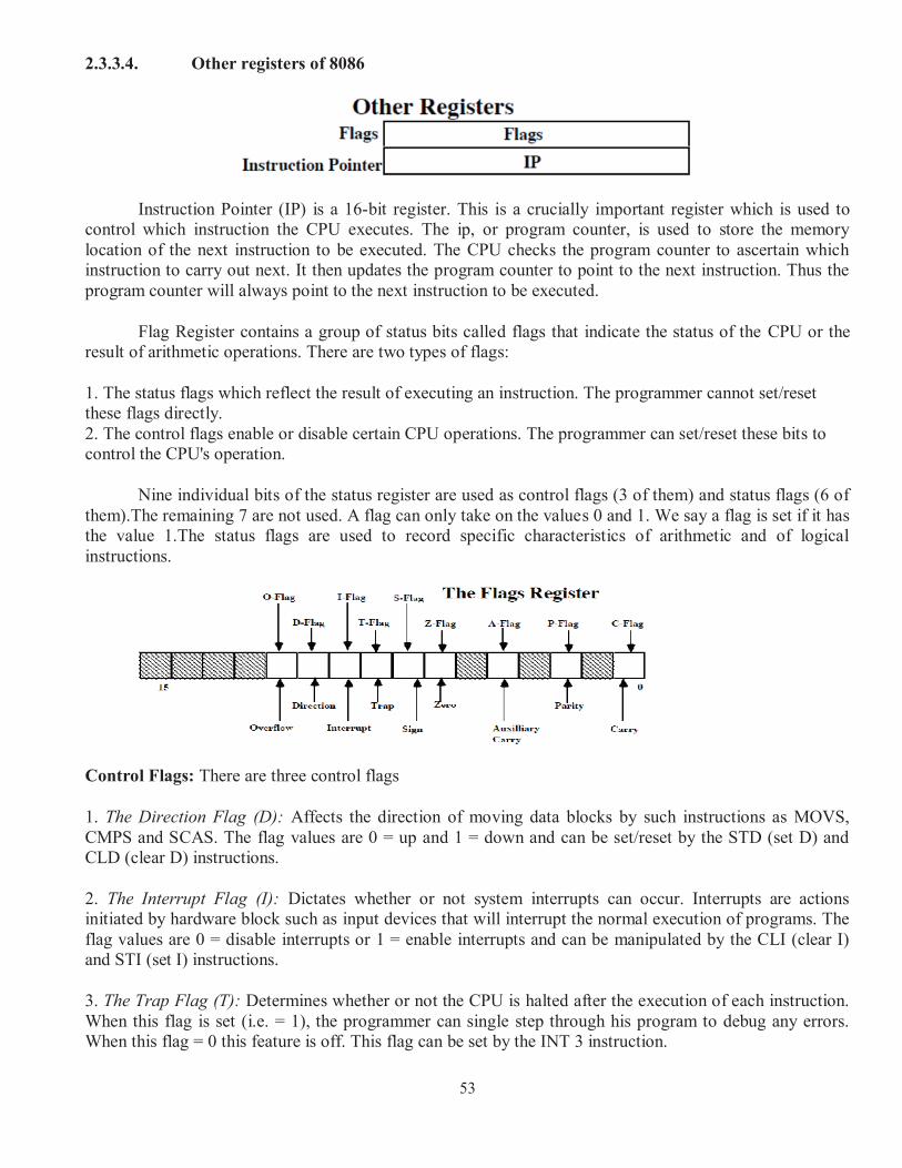
53
2.3.3.4. Other registers of 8086
Instruction Pointer (IP) is a 16-bit register. This is a crucially important register which is used to control which instruction the CPU executes. The ip, or program counter, is used to store the memory location of the next instruction to be executed. The CPU checks the program counter to ascertain which instruction to carry out next. It then updates the program counter to point to the next instruction. Thus the program counter will always point to the next instruction to be executed.
Flag Register contains a group of status bits called flags that indicate the status of the CPU or the result of arithmetic operations. There are two types of flags:
1. The status flags which reflect the result of executing an instruction. The programmer cannot set/reset these flags directly. 2. The control flags enable or disable certain CPU operations. The programmer can set/reset these bits to control the CPU's operation.
Nine individual bits of the status register are used as control flags (3 of them) and status flags (6 of them).The remaining 7 are not used. A flag can only take on the values 0 and 1. We say a flag is set if it has the value 1.The status flags are used to record specific characteristics of arithmetic and of logical instructions.
Control Flags: There are three control flags
1. The Direction Flag (D): Affects the direction of moving data blocks by such instructions as MOVS, CMPS and SCAS. The flag values are 0 = up and 1 = down and can be set/reset by the STD (set D) and CLD (clear D) instructions.
2. The Interrupt Flag (I): Dictates whether or not system interrupts can occur. Interrupts are actions initiated by hardware block such as input devices that will interrupt the normal execution of programs. The flag values are 0 = disable interrupts or 1 = enable interrupts and can be manipulated by the CLI (clear I) and STI (set I) instructions.
3. The Trap Flag (T): Determines whether or not the CPU is halted after the execution of each instruction. When this flag is set (i.e. = 1), the programmer can single step through his program to debug any errors. When this flag = 0 this feature is off. This flag can be set by the INT 3 instruction.
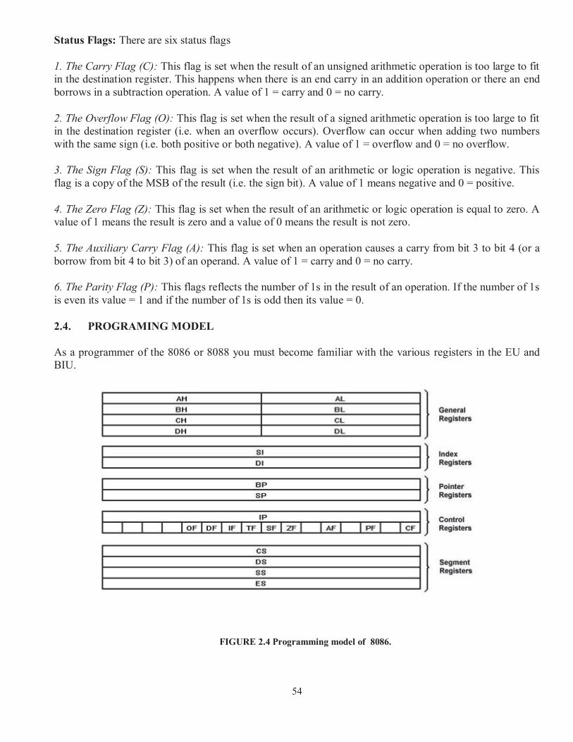
54
Status Flags: There are six status flags
1. The Carry Flag (C): This flag is set when the result of an unsigned arithmetic operation is too large to fit in the destination register. This happens when there is an end carry in an addition operation or there an end borrows in a subtraction operation. A value of 1 = carry and 0 = no carry.
2. The Overflow Flag (O): This flag is set when the result of a signed arithmetic operation is too large to fit in the destination register (i.e. when an overflow occurs). Overflow can occur when adding two numbers with the same sign (i.e. both positive or both negative). A value of 1 = overflow and 0 = no overflow.
3. The Sign Flag (S): This flag is set when the result of an arithmetic or logic operation is negative. This flag is a copy of the MSB of the result (i.e. the sign bit). A value of 1 means negative and 0 = positive.
4. The Zero Flag (Z): This flag is set when the result of an arithmetic or logic operation is equal to zero. A value of 1 means the result is zero and a value of 0 means the result is not zero.
5. The Auxiliary Carry Flag (A): This flag is set when an operation causes a carry from bit 3 to bit 4 (or a borrow from bit 4 to bit 3) of an operand. A value of 1 = carry and 0 = no carry.
6. The Parity Flag (P): This flags reflects the number of 1s in the result of an operation. If the number of 1s is even its value = 1 and if the number of 1s is odd then its value = 0.
2.4. PROGRAMING MODEL
As a programmer of the 8086 or 8088 you must become familiar with the various registers in the EU and BIU.
FIGURE 2.4 Programming model of 8086.