Embed Size (px)
Citation preview
Institute of Solid State PhysicsTechnische Universität Graz
12. Memories /Bipolar transistors
Jan. 9, 2019

Institute of Solid State Physics
ExamsTechnische Universität Graz
January 31March 8May 17June 19October ...
Exam
Calculator is ok. One A4 of handwritten notes.
Explain some concept:(tunnel contact, indirect band gap, thermionic emission, inversion, threshold voltage, ...)
Perform a calculation:(concentration of minority carriers, integrate charge density to find electric field, ...)
Explain how a device works:(JFET, MESFET, MOSFET, laser diode, bipolar transistor, LED, Schottkydiode, Heterojunction bipolar transistor, ...)
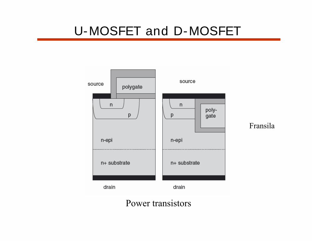
U-MOSFET and D-MOSFET
Power transistors
Fransila
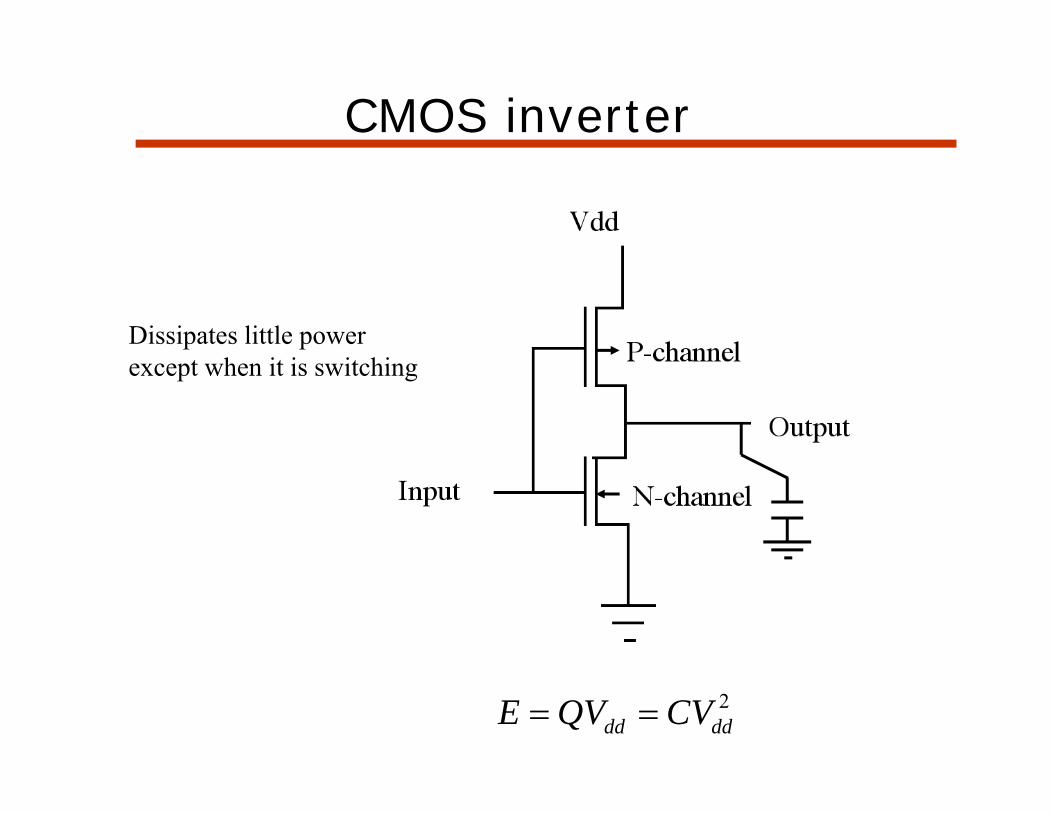
CMOS inverter
2dd ddE QV CV
Dissipates little power except when it is switching
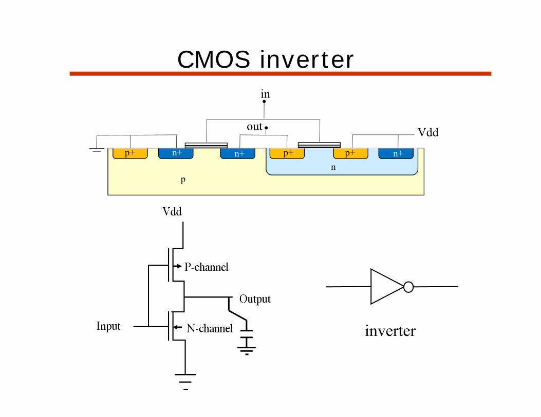
CMOS inverter
out
p
p+ p+p+n
n+n+n+
Vdd
in
inverter
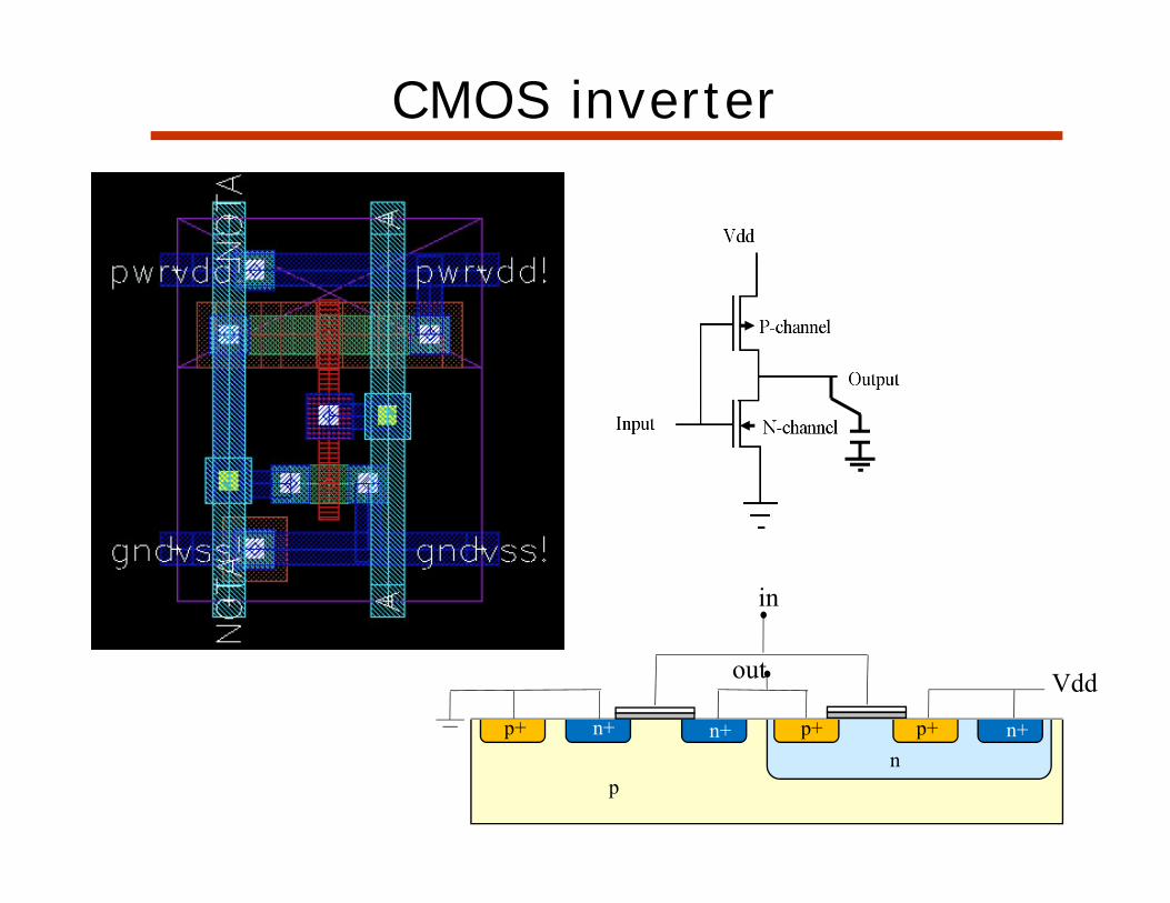
CMOS inverter
out
p
p+ p+p+n
n+n+n+
Vdd
in
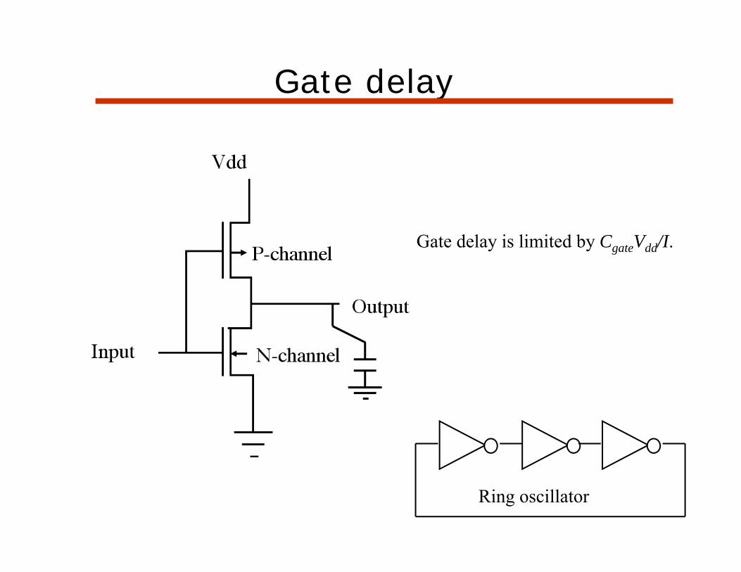
Gate delay
Gate delay is limited by CgateVdd/I.
Ring oscillator
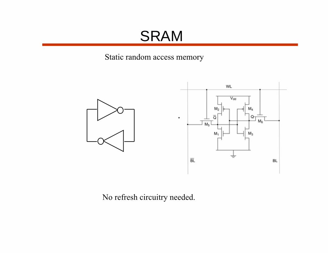
SRAM Static random access memory
No refresh circuitry needed.
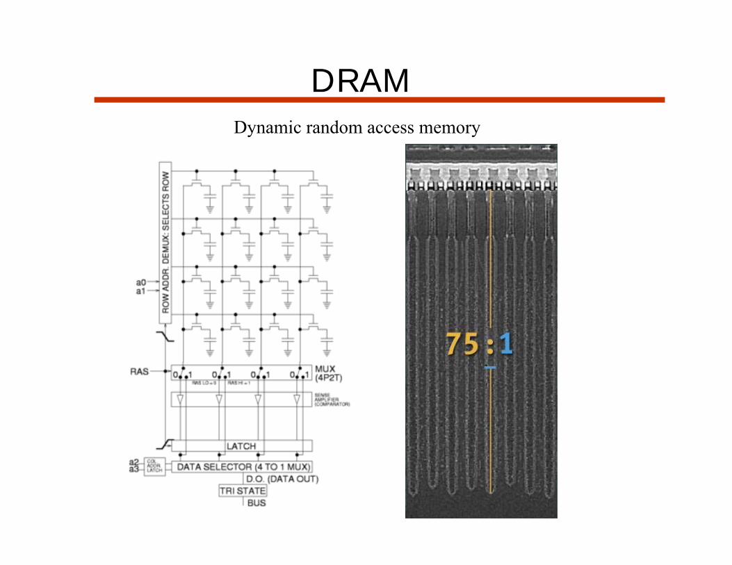
DRAMDynamic random access memory
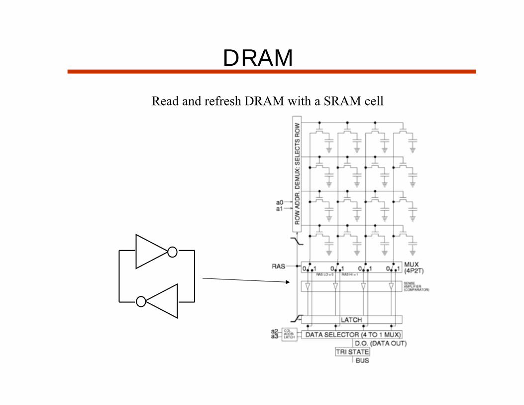
DRAM Read and refresh DRAM with a SRAM cell
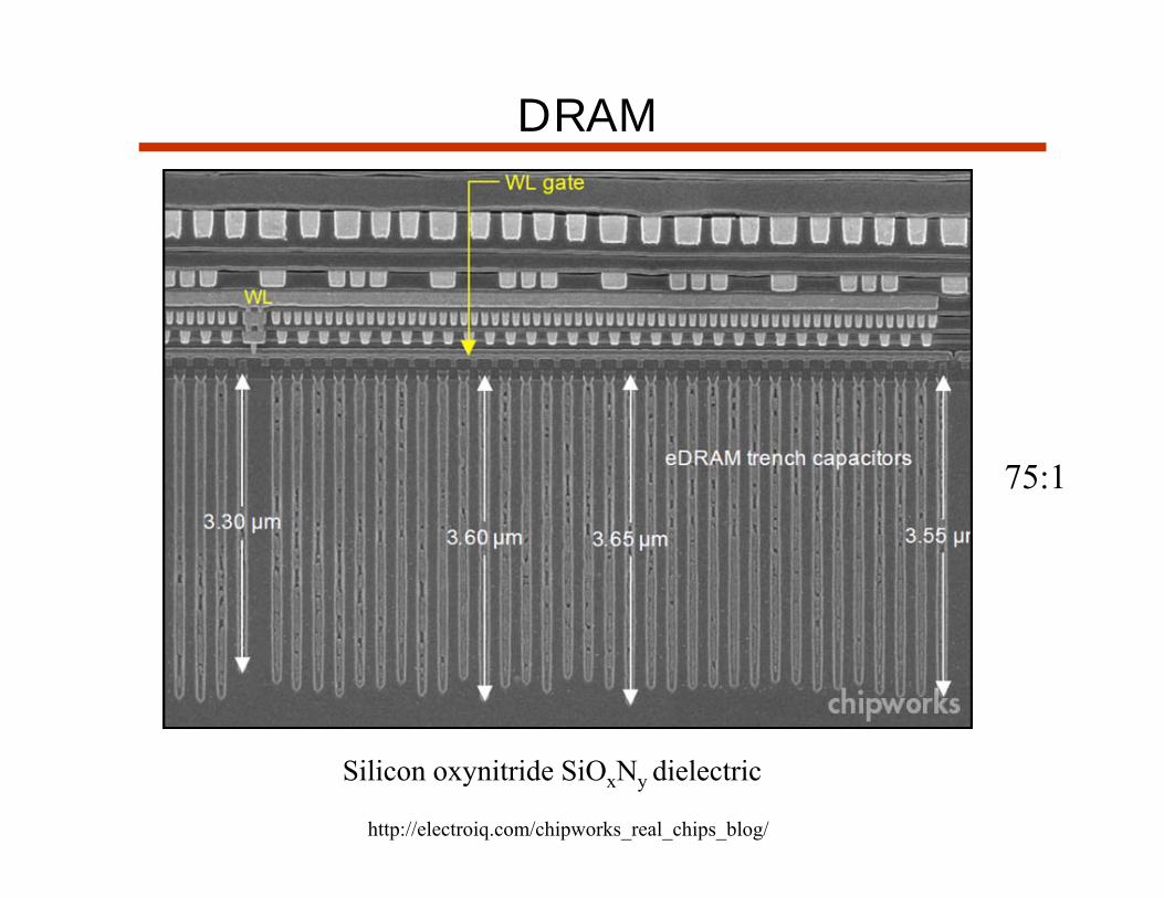
http://electroiq.com/chipworks_real_chips_blog/
DRAM
75:1
Silicon oxynitride SiOxNy dielectric
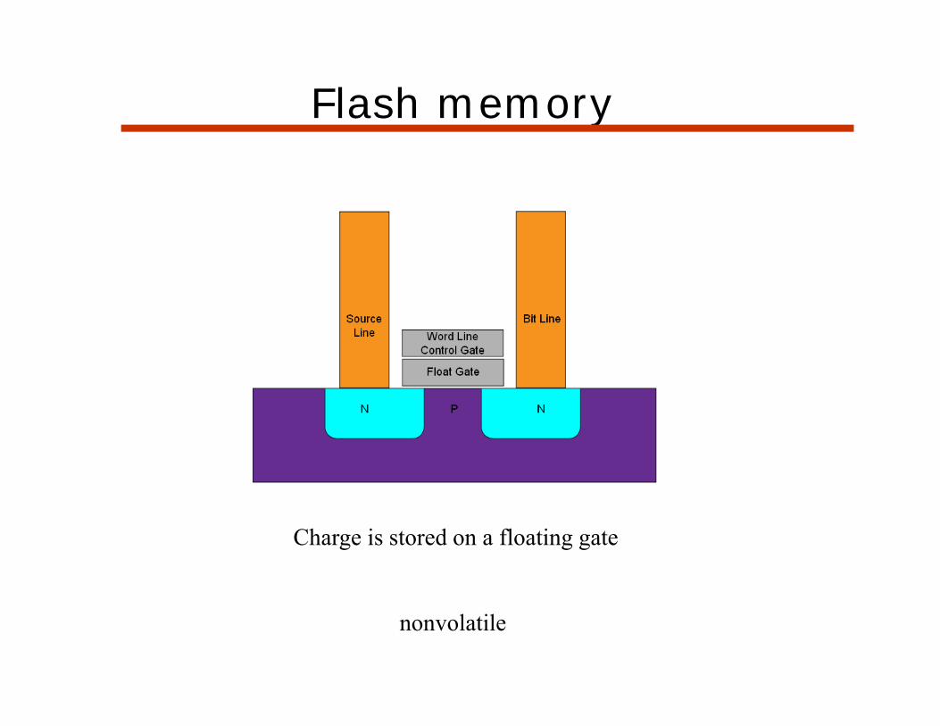
Flash memory
Charge is stored on a floating gate
nonvolatile
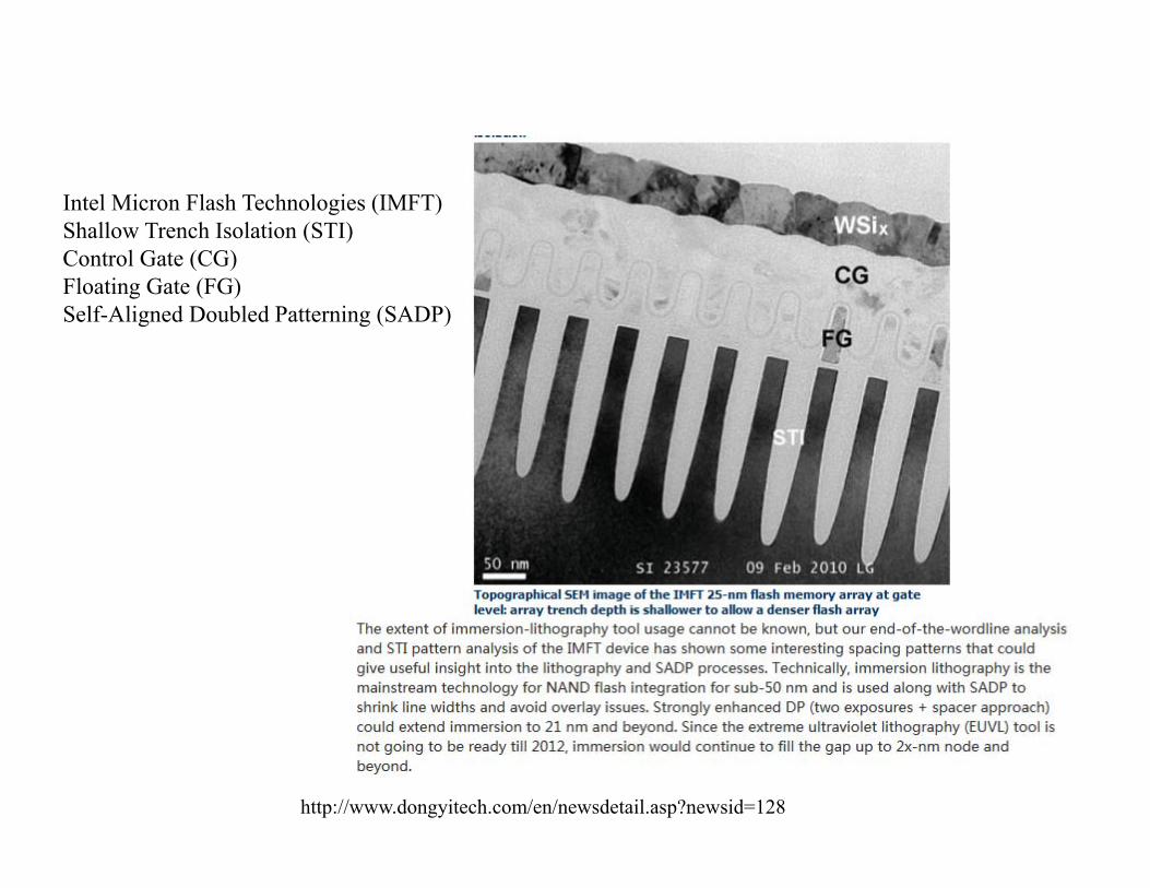
http://www.dongyitech.com/en/newsdetail.asp?newsid=128
Intel Micron Flash Technologies (IMFT)Shallow Trench Isolation (STI)Control Gate (CG)Floating Gate (FG)Self-Aligned Doubled Patterning (SADP)
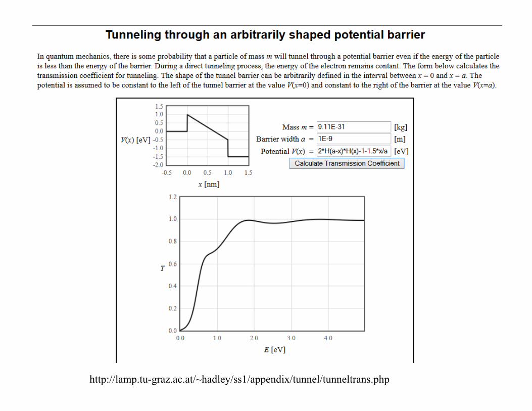
http://lamp.tu-graz.ac.at/~hadley/ss1/appendix/tunnel/tunneltrans.php
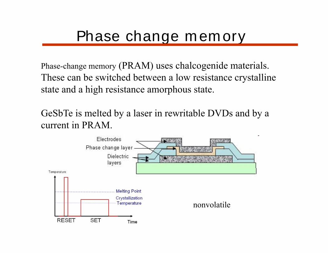
Phase change memory
Phase-change memory (PRAM) uses chalcogenide materials. These can be switched between a low resistance crystalline state and a high resistance amorphous state.
GeSbTe is melted by a laser in rewritable DVDs and by a current in PRAM.
nonvolatile
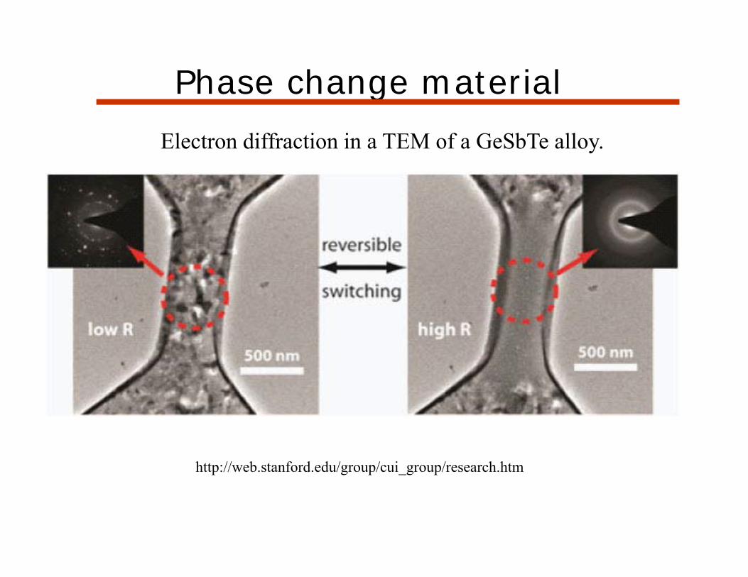
Phase change material Electron diffraction in a TEM of a GeSbTe alloy.
http://web.stanford.edu/group/cui_group/research.htm
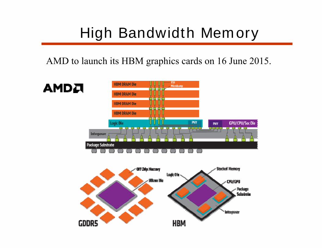
High Bandwidth Memory
AMD to launch its HBM graphics cards on 16 June 2015.
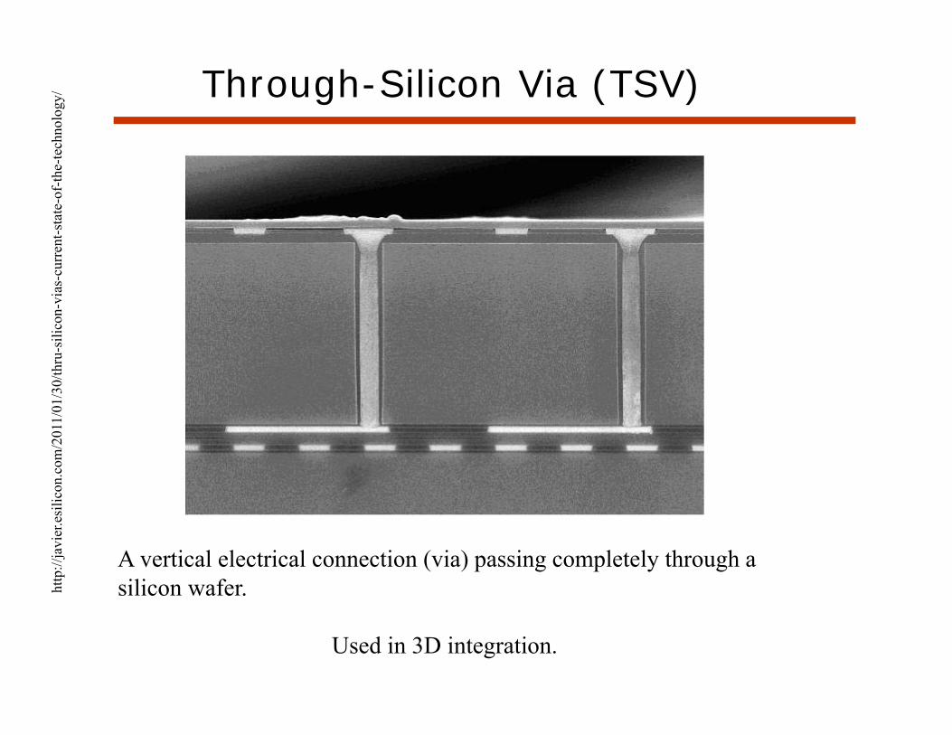
Through-Silicon Via (TSV)
A vertical electrical connection (via) passing completely through a silicon wafer.
Used in 3D integration.
http
://ja
vier
.esi
licon
.com
/201
1/01
/30/
thru
-sili
con-
vias
-cur
rent
-sta
te-o
f-th
e-te
chno
logy
/
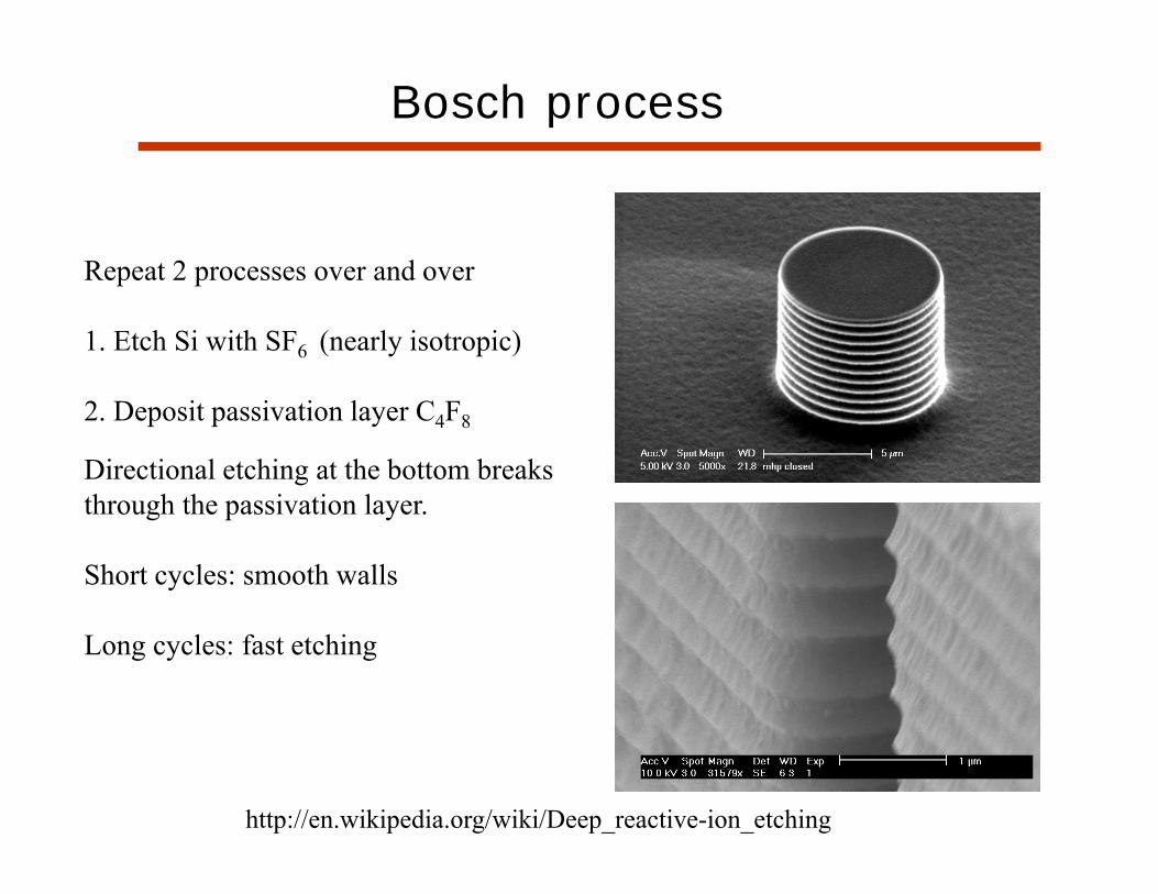
Bosch process
http://en.wikipedia.org/wiki/Deep_reactive-ion_etching
Repeat 2 processes over and over
1. Etch Si with SF6 (nearly isotropic)
2. Deposit passivation layer C4F8
Directional etching at the bottom breaks through the passivation layer.
Short cycles: smooth walls
Long cycles: fast etching
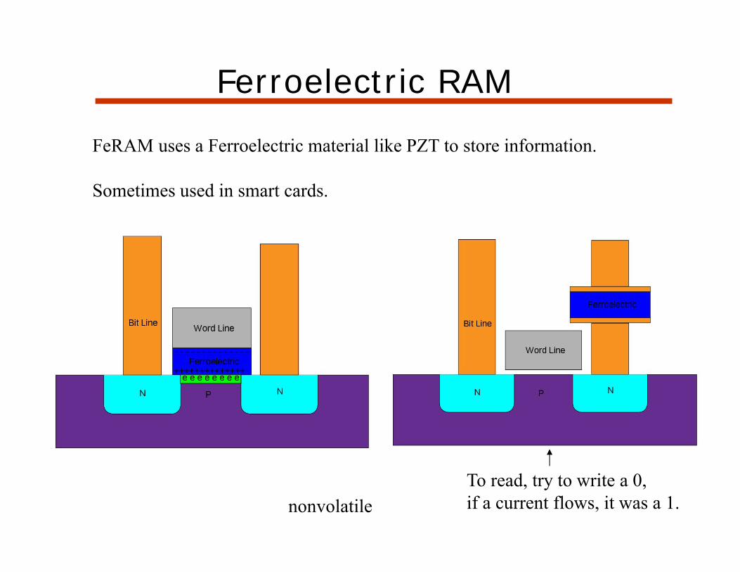
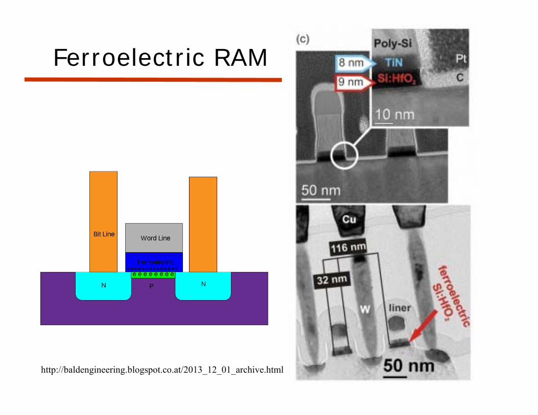
Ferroelectric RAM
FeRAM uses a Ferroelectric material like PZT to store information.
Sometimes used in smart cards.
nonvolatile To read, try to write a 0, if a current flows, it was a 1.
Ferroelectric RAM
http://baldengineering.blogspot.co.at/2013_12_01_archive.html
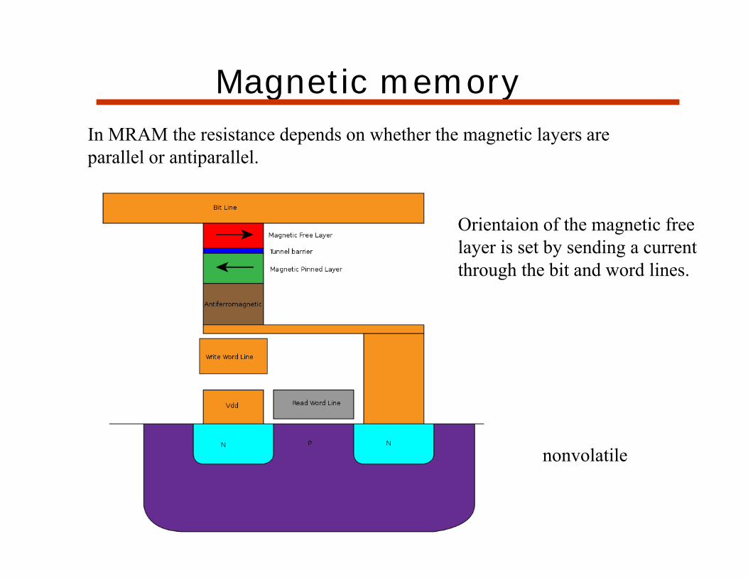
Magnetic memory In MRAM the resistance depends on whether the magnetic layers are parallel or antiparallel.
nonvolatile
Orientaion of the magnetic free layer is set by sending a current through the bit and word lines.
Institute of Solid State Physics
bipolar transistorsTechnische Universität Graz
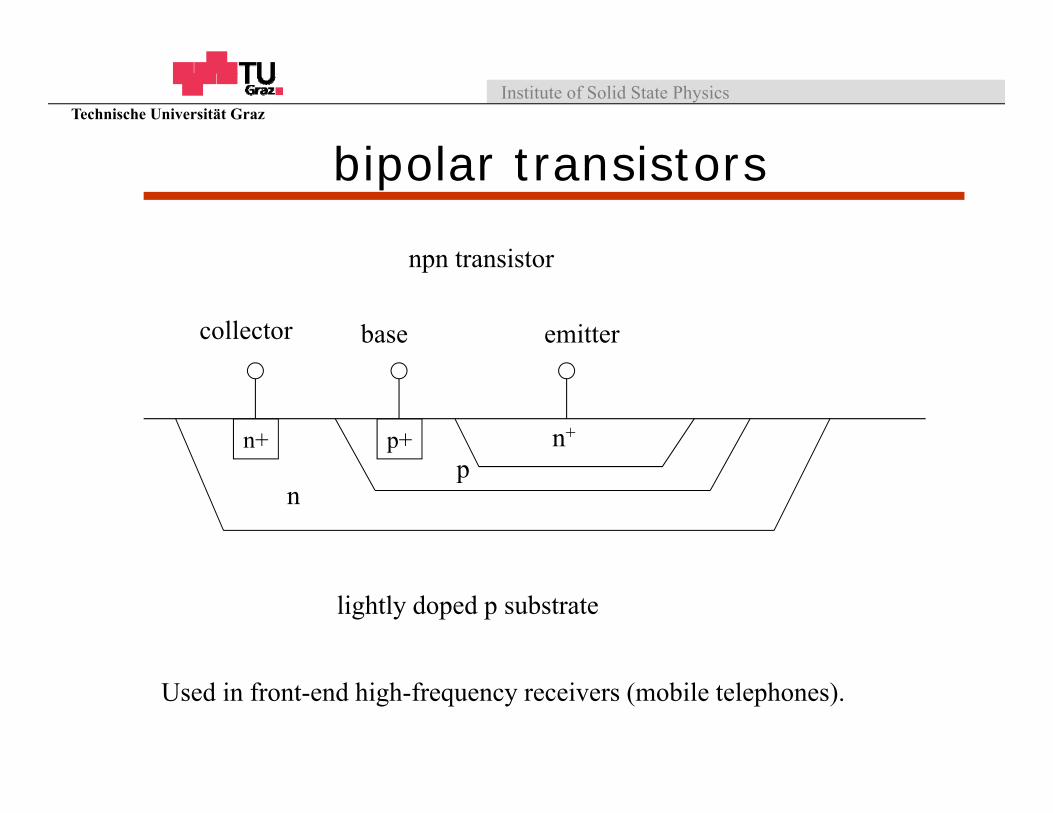
collector base emitter
np
n+
lightly doped p substrate
npn transistor
Used in front-end high-frequency receivers (mobile telephones).
p+n+
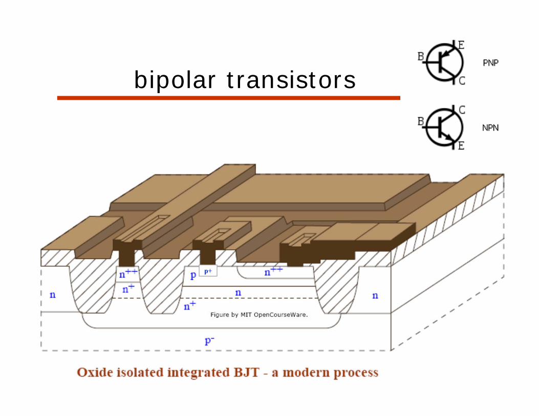
bipolar transistors
p+
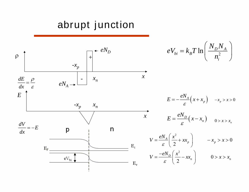
abrupt junction
x
E-xp xn
Ap
eNE x x
Dn
eNE x x
x
-xp
xn
+
-
eND
eNA
2
2
02
02
Ap p
Dn n
eN xV xx x x
eN xV xx x x
0
0
p
n
x x
x x
2ln D Abi B
i
N NeV k Tn
dEdx
dV Edx
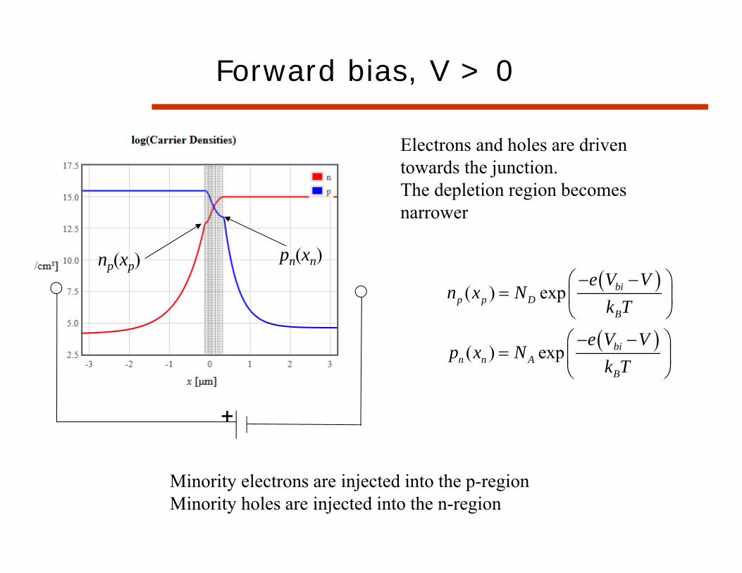
Forward bias, V > 0
Electrons and holes are driven towards the junction.The depletion region becomes narrower
Minority electrons are injected into the p-regionMinority holes are injected into the n-region
np(xp) pn(xn)
+
( ) exp
( ) exp
bip p D
B
bin n A
B
e V Vn x N
k T
e V Vp x N
k T
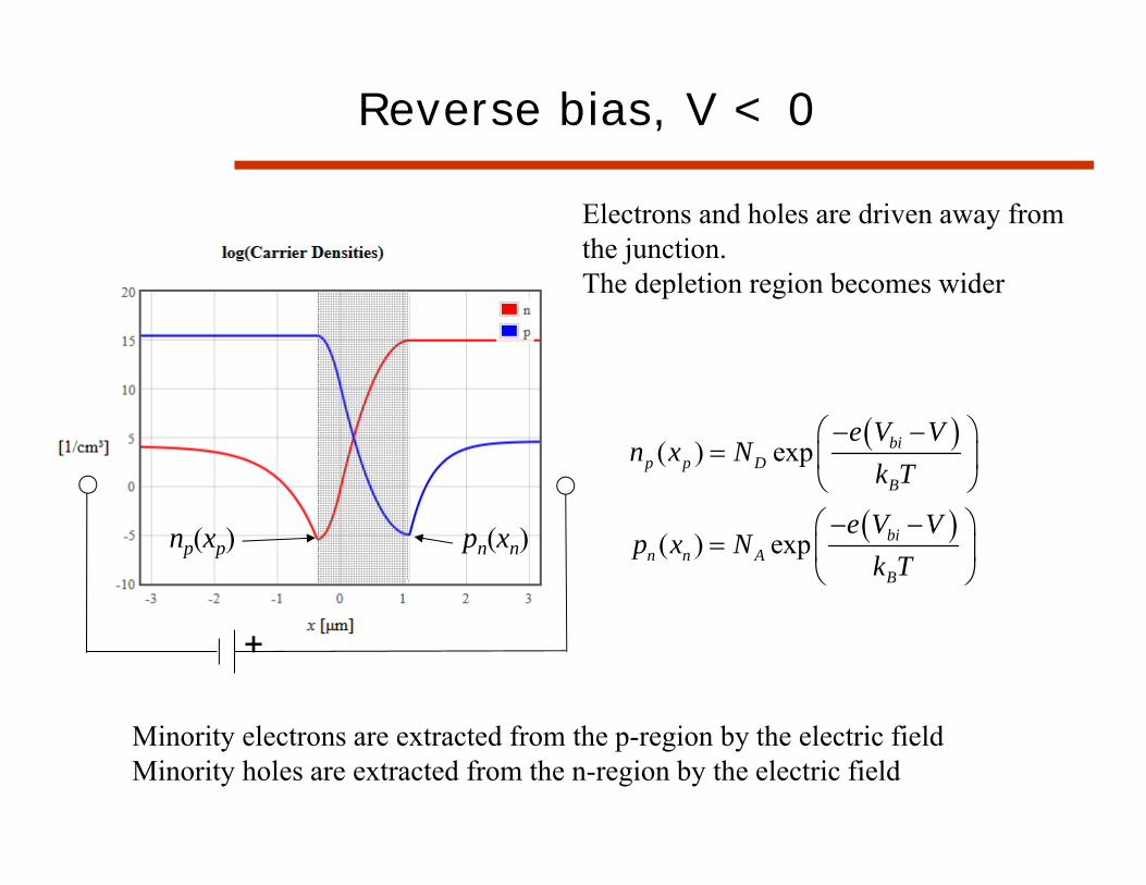
Reverse bias, V < 0
Electrons and holes are driven away from the junction.The depletion region becomes wider
Minority electrons are extracted from the p-region by the electric fieldMinority holes are extracted from the n-region by the electric field
+
np(xp) pn(xn)
( ) exp
( ) exp
bip p D
B
bin n A
B
e V Vn x N
k T
e V Vp x N
k T
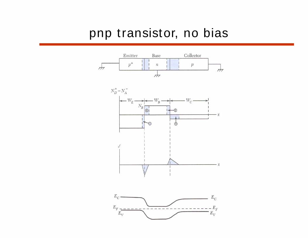
pnp transistor, no bias
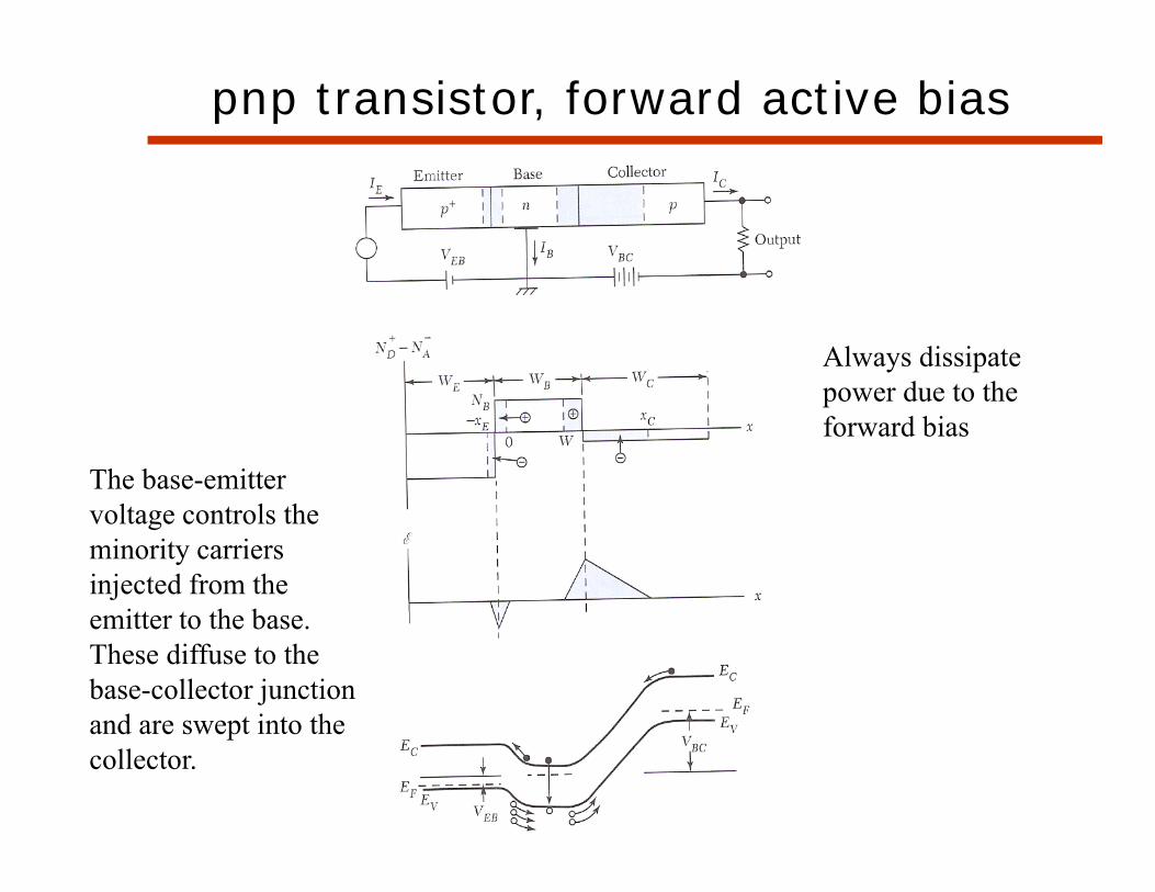
pnp transistor, forward active bias
The base-emitter voltage controls the minority carriers injected from the emitter to the base. These diffuse to the base-collector junction and are swept into the collector.
Always dissipate power due to the forward bias
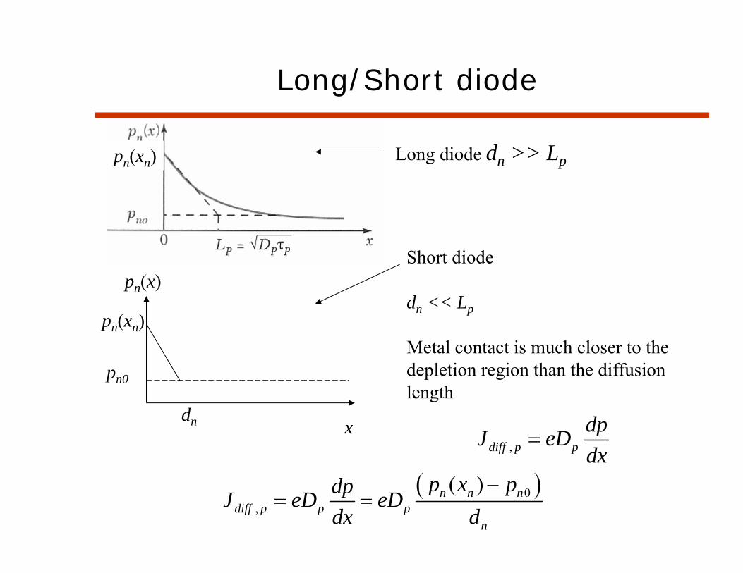
Long/Short diode
n-type
,diff p pdpJ eDdx
0,
( )n n ndiff p p p
n
p x pdpJ eD eDdx d
pn(xn)
pn0
dn x
pn(x)Short diode
dn << Lp
Metal contact is much closer to the depletion region than the diffusion length
Long diode dn >> Lppn(xn)
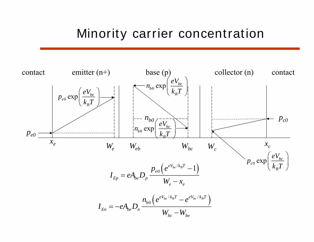
Minority carrier concentration
emitter (n+) base (p) collector (n)contact contact
pe0
nb0 pc0
/0 1be BeV k T
eEp be p
e e
p eI eA D
W x
xe We Web WbcxcWc
/ /0
be B bc BeV k T eV k Tb
En be nbc be
n e eI eA D
W W
0 exp beb
B
eVnk T
0 exp bcb
B
eVnk T
0 exp bee
B
eVpk T
0 exp bcc
B
eVpk T
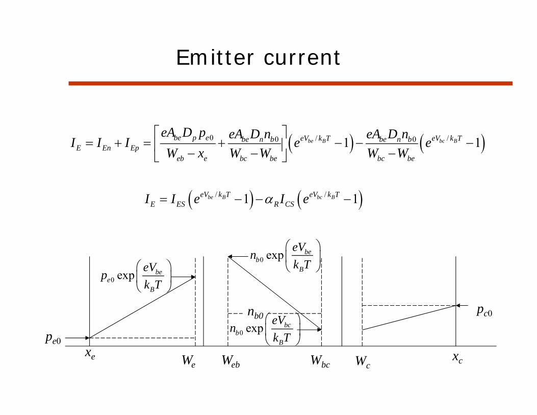
Emitter current
0 / /0 01 1be B bc Bbe p e eV k T eV k Tbe n b be n bE En Ep
eb e bc be bc be
eA D p eA D n eA D nI I I e eW x W W W W
/ /1 1be B bc BeV k T eV k TE ES R CSI I e I e
pe0
nb0 pc0
xe We Web WbcxcWc
0 exp bcb
B
eVnk T
0 exp bee
B
eVpk T
0 exp beb
B
eVnk T
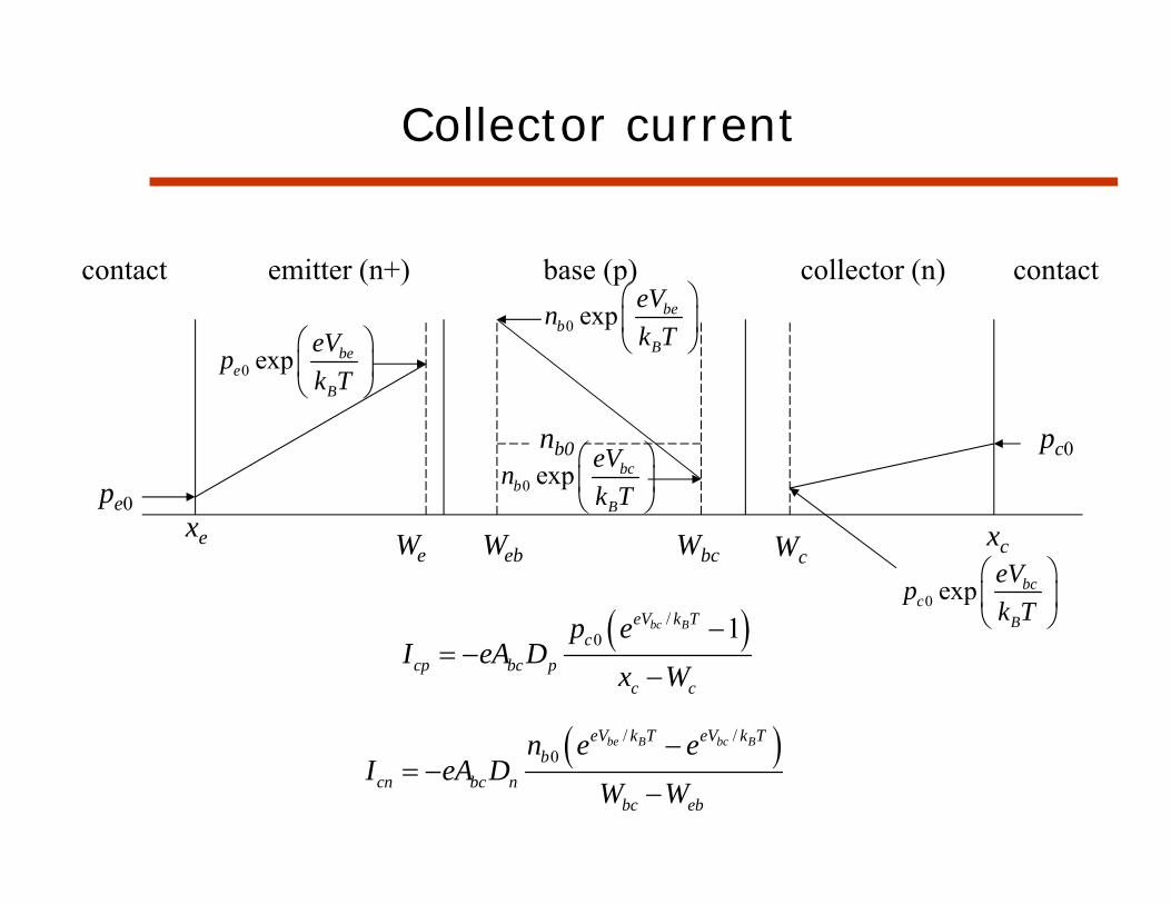
Collector current
emitter (n+) base (p) collector (n)contact contact
/0 1bc BeV k T
ccp bc p
c c
p eI eA D
x W
/ /0
be B bc BeV k T eV k Tb
cn bc nbc eb
n e eI eA D
W W
pe0
nb0 pc0
xe We Web WbcxcWc
0 exp beb
B
eVnk T
0 exp bcb
B
eVnk T
0 exp bee
B
eVpk T
0 exp bcc
B
eVpk T
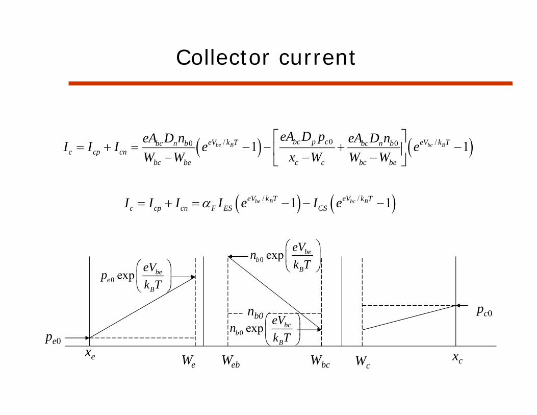
Collector current
0/ /0 01 1be B bc Bbc p ceV k T eV k Tbc n b bc n bc cp cn
bc be c c bc be
eA D peA D n eA D nI I I e eW W x W W W
/ /1 1be B bc BeV k T eV k Tc cp cn F ES CSI I I I e I e
pe0
nb0 pc0
xe We Web WbcxcWc
0 exp bcb
B
eVnk T
0 exp bee
B
eVpk T
0 exp beb
B
eVnk T
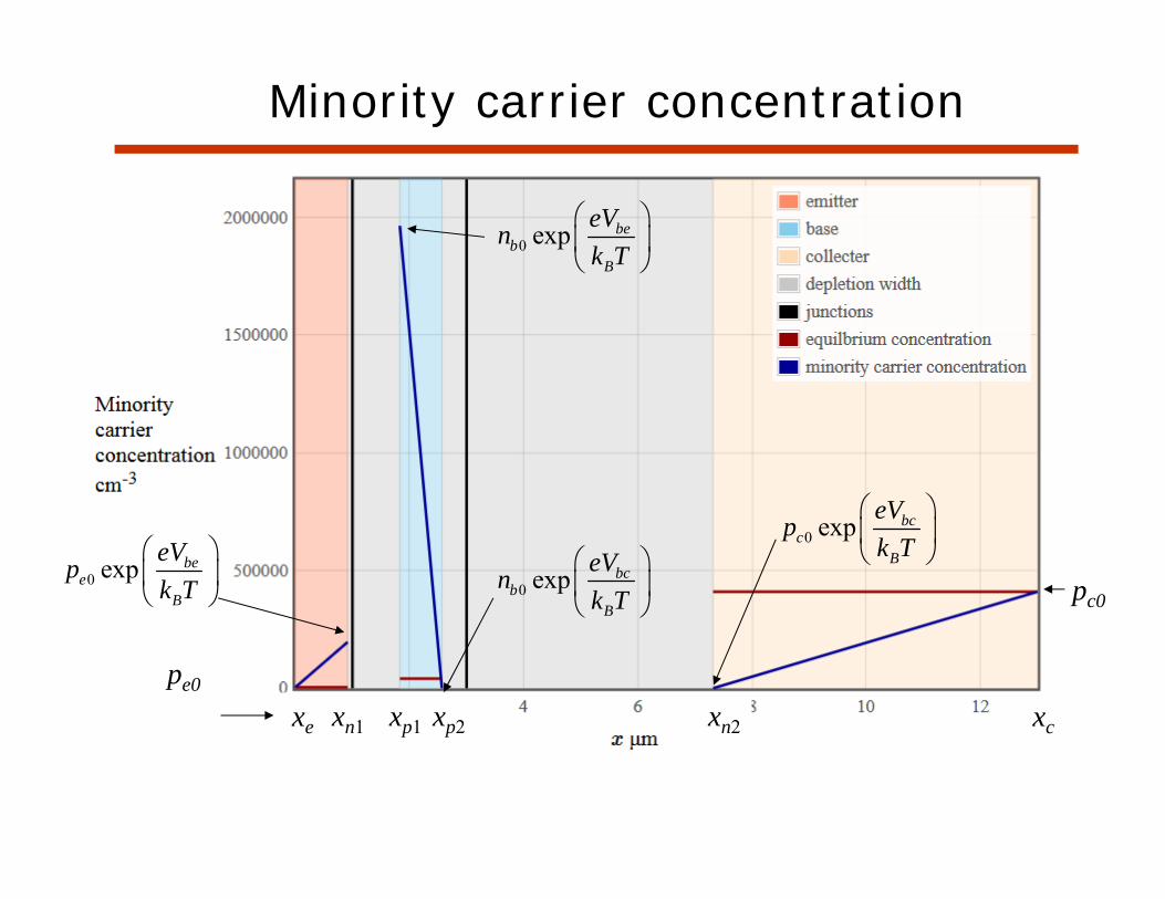
Minority carrier concentration
pe0
pc0
xe xc
0 exp beb
B
eVnk T
0 exp bcb
B
eVnk T
0 exp bee
B
eVpk T
0 exp bcc
B
eVpk T
xn1 xp1 xn2xp2
emitter (n+) base (p) collector (n)contact contact
pe0
nb0 pc0
xe We Web WbcxcWc
0 exp beb
B
eVnk T
0 exp bcb
B
eVnk T
0 exp bee
B
eVpk T
0 exp bcc
B
eVpk T
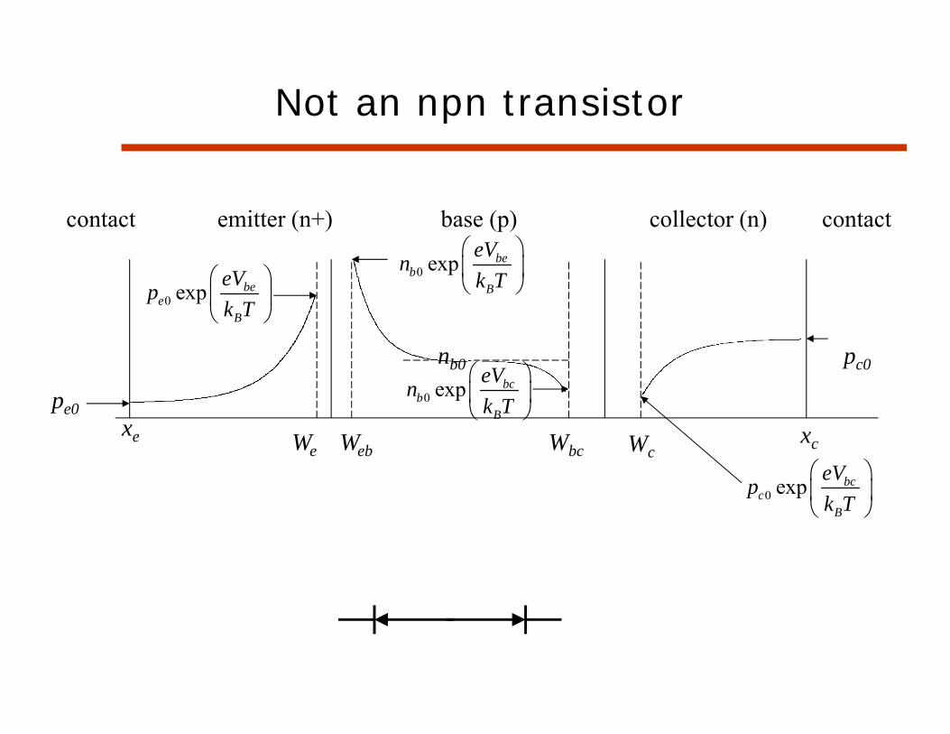
Not an npn transistor
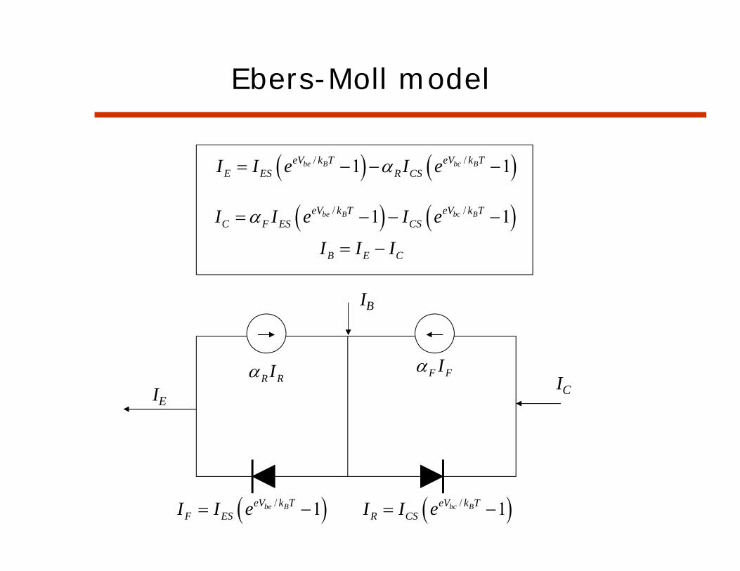
Ebers-Moll model
/ /1 1be B bc BeV k T eV k TC F ES CSI I e I e
/ /1 1be B bc BeV k T eV k TE ES R CSI I e I e
IE
IB
IC
/ 1be BeV k TF ESI I e / 1bc BeV k T
R CSI I e
R RI F FI
B E CI I I
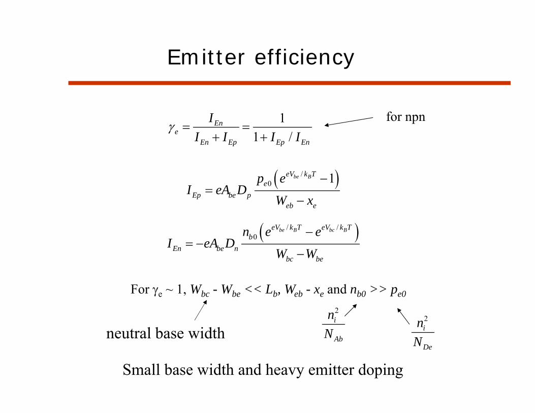
Emitter efficiency
/0 1be BeV k T
eEp be p
eb e
p eI eA D
W x
/ /0
be B bc BeV k T eV k Tb
En be nbc be
n e eI eA D
W W
For e ~ 1, Wbc - Wbe << Lb, Web - xe and nb0 >> pe0
Small base width and heavy emitter doping
for npn
2i
De
nN
2i
Ab
nN
11 /
Ene
En Ep Ep En
II I I I
neutral base width
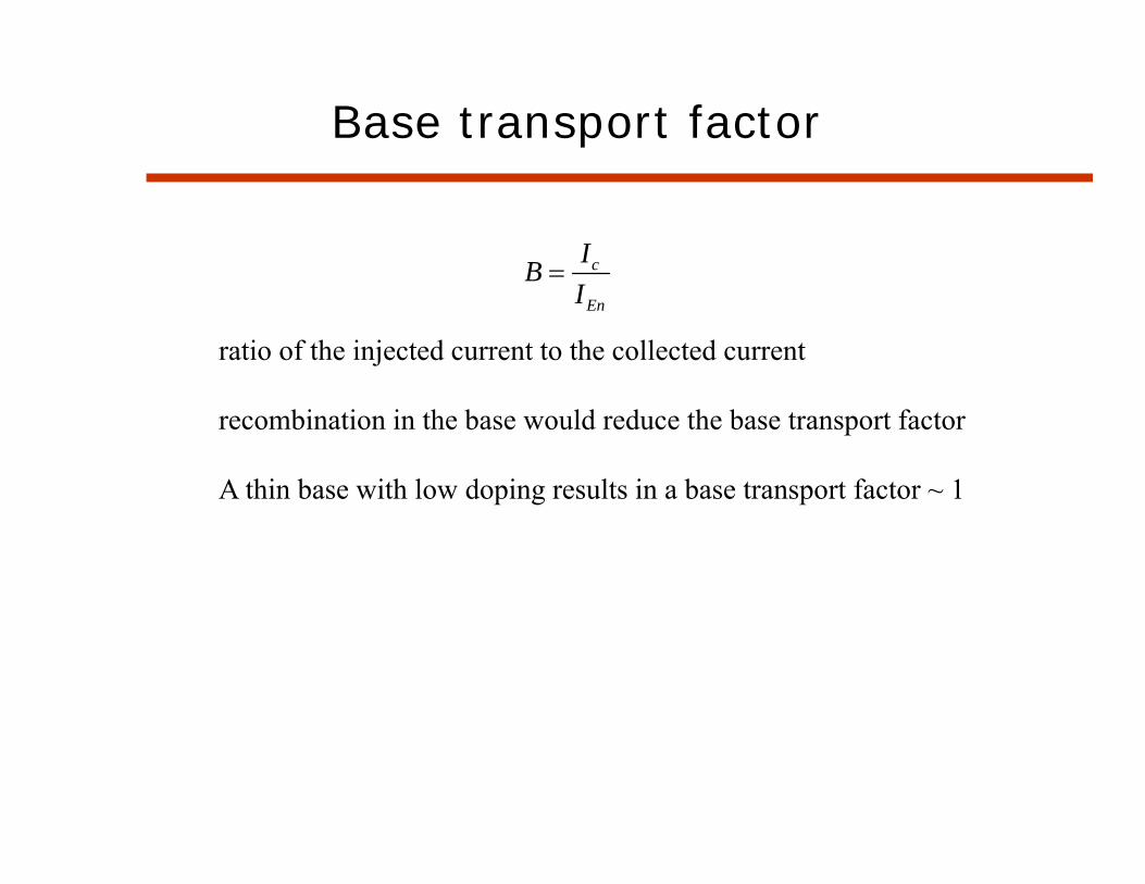
Base transport factor
c
En
IBI
ratio of the injected current to the collected current
recombination in the base would reduce the base transport factor
A thin base with low doping results in a base transport factor ~ 1
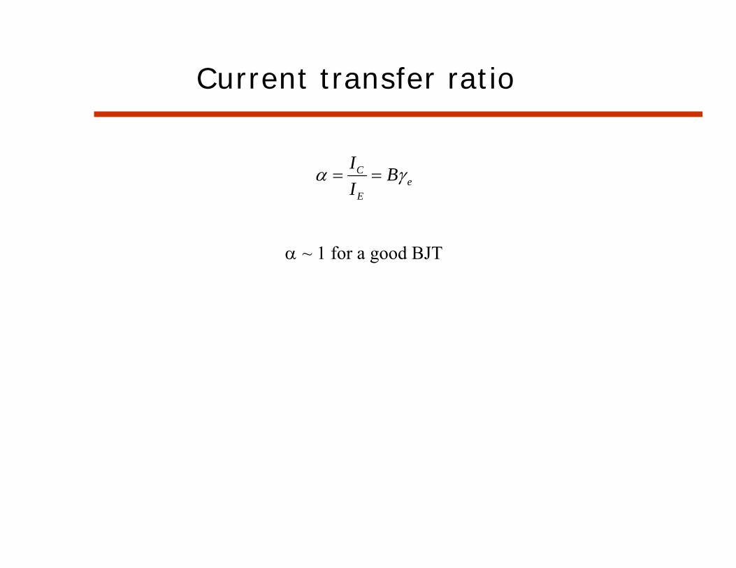
Current transfer ratio
Ce
E
I BI
~ 1 for a good BJT
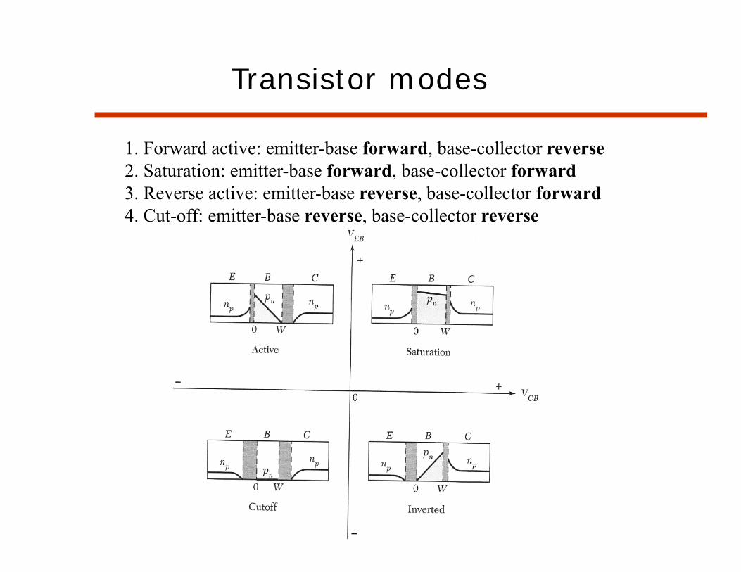
Transistor modes
1. Forward active: emitter-base forward, base-collector reverse2. Saturation: emitter-base forward, base-collector forward3. Reverse active: emitter-base reverse, base-collector forward4. Cut-off: emitter-base reverse, base-collector reverse
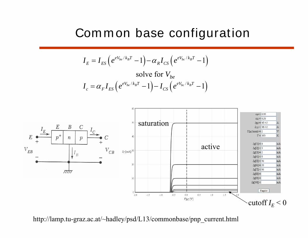
Common base configuration
/ /1 1be B bc BeV k T eV k Tc F ES CSI I e I e
/ /1 1be B bc BeV k T eV k TE ES R CSI I e I e
solve for Vbe
saturation
active
cutoff IE < 0
http://lamp.tu-graz.ac.at/~hadley/psd/L13/commonbase/pnp_current.html