Embed Size (px)
Citation preview

US007855696B2
(12) United States Patent (10) Patent No.: US 7,855,696 B2 Gummalla et al. (45) Date of Patent: Dec. 21, 2010
(54) METAMATERIAL ANTENNA ARRAYS WITH 6,859,114 B2 2/2005 Eleftheriades et al. RADATION PATTERN SHAPNG AND BEAM 7,193,562 B2 3/2007 Shtrom et al. SWITCHING 7,330,090 B2 2/2008 Itoh et al.
(75) Inventors: Ajay Gummala, San Diego, CA (US); 7,391,288 B1 6/2008 Itoh et al. Marin Stoytchev, Chandler, AZ (US); 7,446,712 B2 11/2008 Itoh et al. Maha Achour, San Diego, CA (US); 2004/0164900 A1* 8, 2004 Casabona et al. ........... 342/420 Gregory Poilasne, El Cajon, CA (US) 2005/0253.667 A1 11/2005 Itoh et al.
2007/0010202 A1 1/2007 Yamamoto et al. ......... 455,631 (73) Assignee: Rayspan Corporation, San Diego, CA 2008/0001684 A1 1/2008 Itoh et al.
(US) 2008/00489.17 A1 2/2008 Achour et al.
(*) Notice: Subject to any disclaimer, the term of this 2008/0204327 A1 8/2008 Lee et al. patent is extended or adjusted under 35 2008/0258981 A1* 10, 2008 Achour et al. .............. 343,702 U.S.C. 154(b) by 408 days.
(21) Appl. No.: 12/050,107 FOREIGN PATENT DOCUMENTS
(22) Filed: Mar 17, 2008 JP 50-037323 4, 1975
(65) Prior Publication Data KR 10-2003-022407 3, 2003
US 2008/O258.993 A1 Oct. 23, 2008
Related U.S. Application Data OTHER PUBLICATIONS (60) Provisional application No. 60/918,564, filed on Mar.
16, 2007. Caloz and Itoh, Electromagnetic Metamaterials. Transmission Line s Theory and Microwave Applications, John Wiley & Sons (2006).
(51) Int. Cl. Collin, Field Theory of Guided Waves, John Wiley & Sons, Inc., 2nd H01O 3/24 (2006.01) Ed., Dec. 1990.
(52) U.S. Cl. ............................... 343/876; 343/700 MS; (Continued) 343/853: 342/359
(58) Field of Classification Search .......... 343/700 MS, Primary Examiner Tan Ho 343/853, 876; 342/359
See application file for complete search history. (57) ABSTRACT
(56) References Cited
U.S. PATENT DOCUMENTS
4,014,024 A 3, 1977 Parker et al. 5,874,915 A 2f1999 Lee et al. 6,005,515 A * 12/1999 Allen et al. ................. 342,374 6,489,927 B2 12/2002 LeBlanc et al.
Artea Eisent 10.
Phase shifting or Phase Shifting or Phase Shifting or Delay element delay Element Delay Element
11 111 111
Apparatus, systems and techniques for using composite left and right handed (CRLH) metamaterial (MTM) structure antenna elements and arrays to provide radiation pattern shaping and beam Switching.
45 Claims, 36 Drawing Sheets
Cell fictive Dielestic
Substrate Top Conductive
Feedine Top Conductive Input Feeline
impedance Switching Switching Switching Elstlert Element Element
110 11D
Beam Switching Controlet Ground Plane
Dielectric Substrate h
RF signals Power Combining
and Splitting Module 130
RF signal
Feedback Cotto Rao Transceiver Module 140
Thickless Cell
Conductive Wia

US 7,855,696 B2 Page 2
OTHER PUBLICATIONS
Engheta, N., et al., Metamaterials. Physics and Engineering Explo rations, John Wiley & Sons, Inc., Jul. 2006. Gesbert, D., et al., “From Theory to Practice: An Overview of MIMO Space-Time Coded Wireless Systems.” IEEE Journal Selected Areas in Communications, 21(3):281-302, Apr. 2003. Itoh, T., “Invited Paper: Prospects for Metamaterials.” Electronics Letters, 40(16):972-973, Aug. 2004. Jiang, J.-S., et al., “Comparison of Beam Selection and Antenna Selection Techniques in Indoor MIMO Systems at 5.8 GHz.” Pro ceedings Radio and Wireless Conference (RAWCON), pp. 179-182, Aug. 2003. Lai, A., et al., “Dual-Mode Compact Microstrip Antenna Based on Fundamental Backward Wave.” APMC 2005 Proceedings, vol. 4, pp. 4-7. Dec. 2005. Lai, A., et al., “Infinite Wavelength Resonant Antennas with Monopolar Radiation Pattern Based on Periodic Structures.” IEEE Transactions on Antennas and Propagation, 55(3):868-876, Mar. 2007. Lim, S., et al., “Metamaterial-Based Electronically Controlled Trans mission-Line Structure as a Novel Leaky-Wave Antenna With Tun able Radiation Angle and Beamwidth.” IEEE Transactions on Micro wave Theory and Techniques, 52(12):2678-2690, Dec. 2004.
Pozar, D.M., Microwave Engineering, 3rd Ed., John Wiley & Sons, 2005. Sievenpiper, “High-Impedance Electromagnetic Surfaces.” Ph.D. Dissertation, University of California, Los Angeles, 1999. U.S. Appl. No. 1 1/963,710, filed Dec. 21, 2007, entitled “Power Combiners and Dividers Based on Composite Right and Left Handed Metamaterial Structures” by Dupuy et al. U.S. Appl. No. 12/340,657, filed Dec. 20, 2008, entitled “Multi Metamaterial-Antenna Systems with Directional Couplers” by Lee et al. Waldschmidt, C., et al., “Compact Wide-Band Multimode Antennas for MIMO and Diversity.” IEEE Transactions on Antennas and Propagation, 52(8): 1963-1969, Aug. 2004. Waldschmidt, C., et al., “Complete RF System Model for Analysis of Compact MIMO Arrays.” IEEE Transactions on Vehicular Technol ogy, 53(3):579-586, May 2004. Waldschmidt, C. et al., “Handy MIMO, IEEE Communications Engineer, 3(1):22-25, Feb./Mar. 2005. International Search Report and Written Opinion dated Aug. 21, 2008 for International Application No. PCT/US2008/057255, filed Mar. 17, 2008 (10 pages).
* cited by examiner

U.S. Patent Dec. 21, 2010 Sheet 3 of 36 US 7,855,696 B2
Radiation Radiation Pattern Pattern
#1 #2
160 160
MTM Antenna
MTM Antenna
Array #1 Array #2
RF Signals
150 150 Pattern Pattern Antenna Switching Shaping Shaping Circuit Circuit #1 Circuit #2 170
- - - - - - - - - - - - - - - - - - - - - - - - - - - - N /
Switching Switching Beam Switching Element Element Ooo -- Controller 110 110 120
RF Signals Power Combining
and Splitting Module 130
RF Signal
Radio Transceiver Module 140 F.G. 1C Feedback Control

US 7,855,696 B2 Sheet 4 of 36
?uelº pun010
Dec. 21, 2010 U.S. Patent

US 7,855,696 B2
?uelº punOJS)
U.S. Patent
US 7,855,696 B2 U.S. Patent

U.S. Patent Dec. 21, 2010 Sheet 7 of 36 US 7,855,696 B2

US 7,855,696 B2 Sheet 8 of 36 Dec. 21, 2010 U.S. Patent


US 7,855,696 B2 Sheet 10 of 36 Dec. 21, 2010 U.S. Patent

US 7,855,696 B2
CD
U.S. Patent

U.S. Patent Dec. 21, 2010 Sheet 12 of 36 US 7,855,696 B2

U.S. Patent Dec. 21, 2010 Sheet 13 of 36 US 7,855,696 B2
Vias Connecting Top and Bottom GNDS
U.S. Patent Dec. 21, 2010 Sheet 14 of 36 US 7,855,696 B2
Vias Connection Bottom and Top GND
rWeND Pad
- GND Pad
738 2GND Line
-WGND Line f 734-2
726-2
FIG. 7C

U.S. Patent Dec. 21, 2010 Sheet 15 of 36 US 7,855,696 B2
Vias Connecting Top and Bottom GNDS
730-1/730-2
hTotal Substrate Thickness
Bottom GND
FIG. 7D
Layer Stackup
N Component Side (Layer 1) 1/2 oz cu Finished --- FR4 10 mil +/- 1 mil N GND Plane (Layer 2) 1 oz cu O FR4 35 +/- 1 mil N Power Plane (Layer 3) 1 oz Cu o FR4 10 mi +/- 1 mil N Solder Side (Layer 4) 1/2 oz cu Finished
FIG. 7E

U.S. Patent Dec. 21, 2010 Sheet 16 of 36 US 7,855,696 B2
810
Top Ground
Phase Offset = 0
FIG. 8A
810
Top Ground
Phase Offset = 90°
FIG. 8B

US 7,855,696 B2 U.S. Patent Dec. 21, 2010 Sheet 17 of 36
: FIG. 8C
FIG. 8D

U.S. Patent Dec. 21, 2010 Sheet 18 of 36 US 7,855,696 B2
Ground Electrode MTMAntenna Element
FIG. 9A
MTM Antenna Element Y MTMAntenna Element
FIG. 9B
US 7,855,696 B2 Sheet 19 of 36 Dec. 21, 2010 U.S. Patent
<% 2. \\
FG. 9C

US 7,855,696 B2 Sheet 20 of 36 Dec. 21, 2010 U.S. Patent
- - - - - - - -,- - - - - - -a?e?.a Higo!- - - - - - -N” (’’
, OOZ
(Seefep eSeud

U.S. Patent Dec. 21, 2010 Sheet 21 of 36 US 7,855,696 B2
Distributed MTM
Unit Cell
- 1118
FIG 11A
Branch Feed Line
1121
Branch Feed Line
Distributed CRLH TL. With Perpendicular Stub
- -1 Electrodes
1118 1118
MTM MTM Unit Cell u1 a Unit Cell
1 2
FIG 11B

U.S. Patent Dec. 21, 2010 Sheet 22 of 36 US 7,855,696 B2
1124-1 1124-2
Antenna Element 1
4-Cell MTM MTM Transmission Antenna
Line Element 2
1124-3
1124-4
MTM MTM Antenna
Antenna Element 3 Element 4
FIG. 11C

US 7,855,696 B2 Sheet 23 of 36 Dec. 21, 2010 U.S. Patent
FIG. 11D

US 7,855,696 B2 Sheet 24 of 36 Dec. 21, 2010 U.S. Patent

US 7,855,696 B2 Sheet 25 of 36 Dec. 21, 2010 U.S. Patent

U.S. Patent
18O
18O
Dec. 21, 2010 Sheet 26 of 36 US 7,855,696 B2
270 YZ-plane
Fi", "Y s /
Feed at Port 1
- - - - Feed at Port 2 270
XY-plane F.G. 13B

U.S. Patent Dec. 21, 2010 Sheet 27 of 36 US 7,855,696 B2
CPW CPW MTM Ground Feeline SN, Antenna Feed Line Electrode Slab 1 Element
SNG Slab2
0.00 To TT HIEEE
-2000 || || | | | |
|z1 S -40.00 H
AE -60.00 M MH | | | |
-80.00 1.OO 2.00 3.00 4.00 5.00
FreqGHz) X1 = 2.88GHZX2E 3.54GHz X3E 3.09GHZX4E 2.88GHz Y1c -6.06 Y2 -5.99 Y3c -15.52 Y4-15.38
FIG. 14B

U.S. Patent Dec. 21, 2010 Sheet 28 of 36
Without SNG Slabs O
-23.0 F.G. 14C
With SNG Stabs O
O & 60 7, Xt,Y. y^NSK - 150
U.S. Patent Dec. 21, 2010 Sheet 29 of 36 US 7,855,696 B2
101 Array 2 101
Pattern Shaping Circuit 2 150 Branch Feed
Line
Pattern Pattern Antenna Antenna Array 1 Shaping Shaping Array 3
Circuit 1 Circuit 3
Main Feed
Radio Transceiver Module
F.G. 15A 140
101 Antenna 101
Pattern Shaping
150 Circuit 2
Switch 2
Pattern Shaping Circuit 1
Antenna Array 3
Antenna Array 1
SWitch 1
Main Feed Line Radio Transceiver
Module 140 F.G. 15B

US 7,855,696 B2 Sheet 30 of 36
Main Feed Line
Dec. 21, 2010 U.S. Patent
Main Feed Line

U.S. Patent Dec. 21, 2010 Sheet 31 of 36 US 7,855,696 B2
Microstrip Electrode C Microstrip Electrode (CR,R) LL (CR, L-R)
Port 1 Port 2
Ground onductive Layer
Conductive Via FIG. 17A
2C Y V
Port 1 Port 2
Microstrip Electrode Microstrip Electrode (CR, L-R) (CR, L-R)
Grounded Electrode Stub
FIG. 17B
100
5
SO
-100
Frequency (GHz
F.G. 17C

U.S. Patent Dec. 21, 2010 Sheet 32 of 36 US 7,855,696 B2
Port 2
Port 1 Port 3
FIG. 18A
Main Feed Line
F.G. 18B

U.S. Patent Dec. 21, 2010 Sheet 33 of 36 US 7,855,696 B2
xyzasa N FNAAN) f/N IVINA AIA | | || IWW ITV III |||sts, EE || -- Measured side
2 3 6 4 5 Frequency GHz)
- 1 O
2 O
-3 O
FIG. 18C
O OsCoOS
- 10 n O
g -20 o
30 ET || YAF Simulated S21 den I
-40 -o- Simulated S1 (dB) -O-Measured S21 (dB)
so I MEIT 1 2 3 4 5 6
Frequency (GHz)
FIG. 18O
U.S. Patent Dec. 21, 2010 Sheet 34 of 36 US 7,855,696 B2
O
cyVO CN
V
P pepnufóeW - Cld YO 2. 55
e s f
9:S - pe d O

US 7,855,696 B2 Sheet 35 of 36 Dec. 21, 2010 U.S. Patent

US 7,855,696 B2 Sheet 36 of 36 Dec. 21, 2010 U.S. Patent

US 7,855,696 B2 1.
METAMATERAL ANTENNA ARRAYS WITH RADATION PATTERN SHAPNG AND BEAM
SWITCHING
PRIORITY CLAIM
This application claims the benefits of U.S. Provisional Application Ser. No. 60/918,564 entitled “Metamaterial Antenna Array with Beamforming and Beam-Switching” and filed on Mar. 16, 2007. The entire disclosure of the above patent application is incorporated by reference as part of the specification of this application.
BACKGROUND
This application relates to metamaterial (MTM) structures and their applications for radiation pattern shaping and beam Switching. The propagation of electromagnetic waves in most mate
rials obeys the right handed rule for the (E.H.B) vector fields, where E is the electrical field, His the magnetic field, and B is the wave vector. The phase velocity direction is the same as the direction of the signal energy propagation (group Veloc ity) and the refractive index is a positive number. Such mate rials are “right handed” (RH). Most natural materials are RH materials. Artificial materials can also be RH materials. A metamaterial has an artificial structure. When designed
with a structural average unit cell sizep much smaller than the wavelength of the electromagnetic energy guided by the metamaterial, the metamaterial can behave like a homoge neous medium to the guided electromagnetic energy. Unlike RH materials, a metamaterial can exhibit a negative refractive index with permittivity 6 and permeability p being simulta neously negative, and the phase Velocity direction is opposite to the direction of the signal energy propagation where the relative directions of the (E.H.B) vector fields follow the left handed rule. Metamaterials that Support only a negative index of refraction with permittivity 6 and permeability p being simultaneously negative are “left handed (LH) metamateri als. Many metamaterials are mixtures of LH metamaterials and
RH materials and thus are Composite Left and Right Handed (CRLH) metamaterials. A CRLH metamaterial can behave like a LH metamaterial at low frequencies and a RH material at high frequencies. Designs and properties of various CRLH metamaterials are described in, Caloz, and Itoh, "Electromag netic Metamaterials: Transmission Line Theory and Micro wave Applications,” John Wiley & Sons (2006). CRLH metamaterials and their applications in antennas are described by Tatsuo Itoh in “Invited paper: Prospects for Metamaterials.” Electronics Letters, Vol. 40, No. 16 (August, 2004). CRLH metamaterials can be structured and engineered to
exhibit electromagnetic properties that are tailored for spe cific applications and can be used in applications where it may be difficult, impractical or infeasible to use other materials. In addition, CRLH metamaterials may be used to develop new applications and to construct new devices that may not be possible with RH materials.
SUMMARY
This application includes apparatus, systems and tech niques for using MTM antenna elements and arrays to pro vide radiation pattern shaping and beam Switching.
In one aspect, an antenna system includes antenna ele ments that wirelessly transmit and receive radio signals, each
10
15
25
30
35
40
45
50
55
60
65
2 antenna element configured to include a composite left and right handed (CRLH) metamaterial (MTM) structure; a radio transceiver module in communication with the antenna ele ments to receive a radio signal from or to transmit a radio signal to the antenna elements; a power combining and split ting module connected in signal paths between the radio transceiver module and the antenna elements to split radio power of a radio signal directed from the radio transceiver module to the antenna elements and to combine power of radio signals directed from the antenna elements to the radio transceiver module; Switching elements that are connected in signal paths between the power combining and splitting mod ule and the antenna elements, each Switching element to activate or deactivate at least one antenna element in response to a Switching control signal; and a beam Switching controller in communication with the Switching elements to produce the Switching control signal to control each Switching element to activate at least one Subset of the antenna elements to receive or transmit a radio signal. One implementation of the above system can include a
dielectric substrate on which the antenna elements are formed; a first conductive layer supported by the dielectric Substrate and patterned to comprise (1) a first main ground electrode that is patterned to comprise a plurality of separate coplanar waveguides to guide and transmit RF signals, (2) a plurality of separate cell conductive patches that are separated from the first main ground electrode, and (3) a plurality of conductive feed lines. Each conductive feed line includes a first end connected to a respective coplanar waveguide and a second end electromagnetically coupled to a respective cell conductive patch to carry a respective RF signal between the respective co-planar waveguide and the respective cell con ductive patch. This implementation includes a second con ductive layer supported by the dielectric substrate that is separate from and parallel to the first conductive layer. The second conductive layer is patterned to include (1) a second main ground electrode in a footprint projected to the second conductive layer by the first ground electrode, (2) cell ground conductive pads that are respectively located in footprints projected to the second conductive layer by the cell conduc tive patches, and (3) ground conductive lines that connect the cell ground conductive pads to the second main ground elec trode, respectively. Cell conductive via connectors are formed in the Substrate, each cell conductive via connection connecting a cell conductive patch in the first conductive layer and a cell ground pad in the second conductive layer in the footprint projected by the cell conductive path and ground via connectors are formed in the substrate to connect the first main ground electrode in the first conductive layer and the second main ground electrode in the second conductive layer. Each cell conductive patch, the substrate, a respective cell conductive via connector and the cell ground conductive pad, a respective co-planar waveguide, and a respective electro magnetically coupled conductive feed line are structured to form a composite left and right handed (CRLH) metamaterial structure as one antenna element.
In another aspect, an antenna system includes antenna arrays and pattern shaping circuits that are respectively coupled to the antenna arrays. Each antenna array is config ured to transmit and receive radiation signals and includes antenna elements that are positioned relative to one another to collectively produce a radiation transmission pattern. Each antenna element includes a composite left and right handed (CRLH) metamaterial (MTM) structure. Each pattern shap ing circuit Supplies a radiation transmission signal to a respective antenna array and produces and directs replicas of the radiation transmission signal with selected phases and
US 7,855,696 B2 3
amplitudes to the antenna elements in the antenna array, respectively, to generate a respective radiation transmission pattern associated with the antenna array. This system also includes an antenna Switching circuit coupled to the pattern shaping circuits to Supply the radiation transmission signal to at least one of the pattern shaping circuits and configured to selectively direct the radiation transmission signal to at least one of the antenna arrays at a time to transmit the radiation transmission signal.
In another aspect, an antenna system includes antenna ele ments. Each antenna element is configured to include a com posite left and right handed (CRLH) metamaterial (MTM) structure. This system includes pattern shaping circuits, each of which is coupled to a Subset of the antenna elements and operable to shape a radiation pattern associated with the Sub set of the antenna elements. An antenna Switching circuit is included in this system and is coupled to the pattern shaping circuits that activates at least one Subset at a time to generate the radiation pattern associated with the at least one Subset. The activation is Switched among the Subsets as time passes based on a predetermined or adaptive control logic.
In yet another aspect, a method of shaping radiation pat terns and Switching beams based on an antenna system having antenna elements includes receiving a main signal from a main feed line; providing split paths from the main feed line by using a radial power combiner/divider, to transmit a signal on each path to one of a plurality of pattern shaping circuits; shaping a radiation pattern associated with a Subset of antenna elements by using the pattern shaping circuit that is coupled to the Subset; and activating at least one Subset at a time to generate the radiation pattern associated with the at least one subset. The activation is switched among the subsets as time passes based on predetermined or adaptive control logic and a composite left and right handed (CRLH) metama terial (MTM) structure is used to form each of the antenna elements.
These and other implementations and their variations are described in detail in the attached drawings, the detailed description and the claims.
BRIEF DESCRIPTION OF THE DRAWINGS
FIGS. 1A, 1B and 1C show examples of MTM antenna systems having MTM antenna arrays with radiation pattern shaping and beam Switching.
FIG. 2 shows an example of a CRLH MTM transmission line with four unit cells.
FIGS. 2A, 2B, 2C, 2D, 3A, 3B and 3C show equivalent circuits of the device in FIG. 2 under different conditions in transmission line mode and antenna mode.
FIGS. 4A and 4B show examples of the resonant position along the beta curves in the device in FIG. 2.
FIGS. 5A and 5B show an example of a CRLH MTM device with a truncated ground conductive layer design. FIG.5C shows an example of a CRLHMTM antenna with
four MTM cells with a truncated ground conductive layer design based on the structure in FIG. 5A.
FIGS. 6A and 6B show another example of a CRLH MTM device with a truncated ground conductive layer design.
FIG. 6C shows an example of a CRLH MTM antenna with four MTM cells with a truncated ground conductive layer design based on the structure in FIG. 6A.
FIG. 7A shows the 3-D view of an example of a 2-antenna MTM array.
FIG.7B shows the top layer of the 2-antenna MTM array in FIG. 7A.
5
10
15
25
30
35
40
45
50
55
60
65
4 FIG. 7C shows the bottom layer of the 2-antenna array in
FIG. 7A. FIG. 7D shows the side view of the Substrate in FIG. 7A. FIG. 7E shows an example of a FR4 printed circuit board
for forming the structure shown in FIGS. 7A-7D. FIGS. 8A, 8B, 8C and 8D show two examples of 2-antenna
MTM arrays with a phase combining device for shaping the radiation pattern: (1) phase offset 0 degree, mechanical con figuration and the corresponding radiation pattern; (2) phase offset=90 degrees. FIG.9A shows the 3-D view of an example of a 2-antenna
MTM array with a Wilkinson power divider. FIG.9B shows the top view of the 2-antenna MTM array
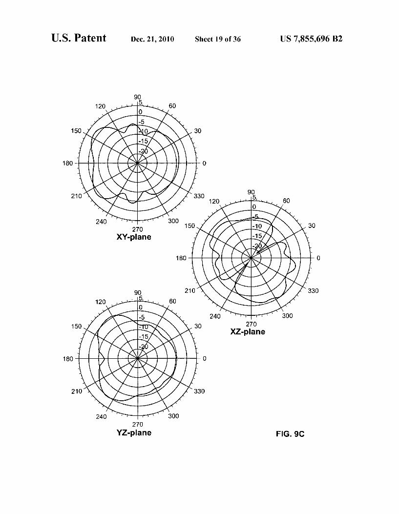
with the Wilkinson power divider. FIG. 9C shows radiation patterns of the 2-antenna MTM
array with the Wilkinson power divider in three different planes.
FIG. 10 shows the phase response of a CRLH transmission line which is a combination of the phase of the RH transmis sion line and the phase of the LH transmission line.
FIGS. 11A and 11B show a distributed MTM unit cell and a Zero degree CRLH transmission line based on the MTM unit cell.
FIG. 11C shows an example of a 4-antenna MTM array with a zero degree CRLH transmission line for shaping the radiation pattern.
FIG. 11D shows radiation patterns of the 4-antenna MTM array with the Zero degree CRLH transmission line in three different planes.
FIG. 12 shows an example of a four-port directional cou pler with coupling magnitudes and phases for four different paths.
FIG. 13A shows an example of a 2-antenna MTM array with a directional MTM coupler for shaping the radiation pattern.
FIG. 13B shows radiation patterns of the 2-antenna MTM array with the directional MTM coupler in three different planes.
FIG. 14A shows an example of a 2-antenna MTM array with SNG slabs for shaping the radiation pattern. FIG.14B shows simulated magnitudes of the S-parameters
of the 2-antenna MTM array with the SNG slabs. FIG. 14C shows radiation patterns of the 2-antenna MTM
array without the SNG slabs. FIG. 14D shows radiation patterns of the 2-antenna MTM
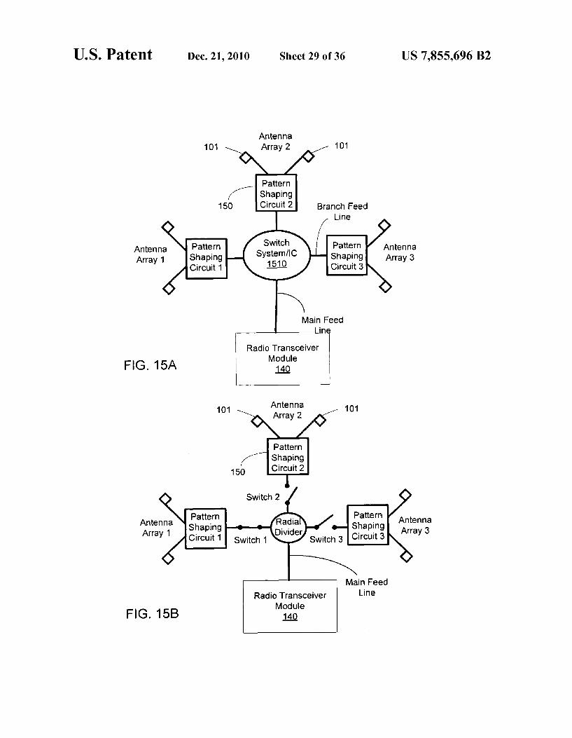
array with the SNG slabs. FIGS. 15A and 15B show two examples of an antenna
switching circuit in FIG. 1C. FIG. 16A shows an example of a conventional N-port
radial power combiner/divider. FIG. 16B shows an example of an N-port radial power
combiner/divider using a Zero degree CRLH transmission line.
FIGS. 17A and 17B shows examples of MTM unit cells based on lumped components.
FIG. 17C shows the phase response of the Zero degree CRLH transmission line used for the 2-port transmission line with a single MTM unit cell in FIG. 17B.
FIG. 18A shows an example of a conventional 3-port radial power combiner/divider.
FIG. 18B shows an example of a 3-port radial power com biner/divider using a zero degree CRLH transmission line.
FIG. 18C shows simulated and measured magnitudes of the S-parameters for the conventional 3-port radial power combiner/divider in FIG. 18A.
US 7,855,696 B2 5
FIG. 18D shows simulated and measured magnitudes of the S-parameters for the 3-port radial power combiner/divider using the Zero degree CRLH transmission line.
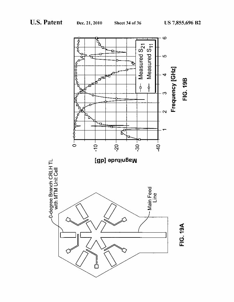
FIG. 19A shows an example of a 5-port radial power com biner/divider using a zero degree CRLH transmission line.
FIG. 19B shows measured magnitudes of the S-parameters of the 5-port radial power combiner/divider using the Zero degree CRLH transmission line in FIG. 19A.
FIG. 20A shows an example of an antenna system with 6-antenna elements for radiation pattern shaping and beam Switching.
FIG. 20B shows radiation patterns of the three antenna subsets in the antenna system in FIG. 20A.
FIG. 21 shows an example of an antenna system with 12-antenna elements for radiation pattern shaping and beam Switching.
In the appended figures, similar components and/or fea tures may have the same reference numeral. Further, various components of the same type may be distinguished by fol lowing the reference numeral by a dash and a second label that distinguishes among the similar components. If only the first reference numeral is used in the specification, the description is applicable to any one of the similar components having the same first reference numeral irrespective of the second refer ence numeral.
DETAILED DESCRIPTION
Metamaterial (MTM) structures can be used to construct antennas and other electrical components and devices. The present application describes examples of multiple MTM antennas configured to be used in WiFi access points (AP), base-stations, micro base-stations, laptops, and other wireless communication devices that require higher Signal-to-Noise Ratio (SNR) to increase the throughput and range, while at the same time minimizing interference. The present applica tion describes, among others, techniques, apparatuses and systems that employ composite left and right handed (CRLH) metamaterials for shaping radiation patterns and beam Switching antenna Solutions.
Specifically, the antenna array designs in this application use CLRH metamaterials to construct compact antenna arrays in a radiation pattern shaping and beam Switching antenna system. Arrays of multiple MTM antennas are used to build an antenna system that is capable of Switching among multiple beam patterns depending on an operational require ment or preference, e.g., the wireless link communication status. Such an antenna system using antennas made from CLRH metamaterials can be designed to retain the benefits of the conventional Smart antenna systems and provide addi tional benefits that are not available or difficult to achieve with conventional Smart antenna systems. The reduction in antenna size based on MTM structures allows CRLH MTM antenna arrays to be adapted for a wide range of antenna improvements.
In the examples described in this application, each beam pattern is created from a single antenna element or by com bining signals from a corresponding antenna Subset of mul tiple antenna elements. The layout of the antenna elements within the antenna array is geometrically designed in con junction with a single antenna pattern and desired beam pat terns. Various techniques to shape radiation patterns are pre sented in this application. Some examples include phase shifting, power combining and coupling circuits. The described antenna systems implement an antenna
Switching circuit that activates at least one Subset of the beam patterns based on the communication link status or other
10
15
25
30
35
40
45
50
55
60
65
6 requirements. Switching elements, such as diodes and RF Switch ICs, are used along the traces connecting the antenna elements to a power combining and splitting module that interfaces with the RF transceiver module. The switching elements may be placed at a distance that is multiple of W/2. where w is the wavelength of the propagating wave, from the radial power combining and splitting module to improve matching conditions. The RF transceiver module includes an analog front end connected to the power combining and split ting module, an analog-to-digital conversion block, and a digital signal processor in the backend that performs digital processing on a received signal and generates an outgoing transmission signal. This digital processor can perform Vari ous signal processing operations on a received signal, such as evaluating the packet error rate of the received signal or determining the relative signal strength intensity (RSSI) of the received signal. The MTM radiation pattern shaping and beam switching
antenna system can Support multiple bands provided that the switches or diodes are multi-bands as well. The radial power combiner/divider, couplers, and delay lines can be designed to Support multiple bands. In some implementations, Electro magnetic Band Gap (EBG) structures can be printed in the vicinity of antennas to modify antenna radiation patterns. The antenna systems described in this application can be
formed on various circuit platforms. For example, FR-4 printed circuit boards can be used to support the RF structures and antenna elements described in this application. In addi tion, the RF structures and antenna elements described in this application can be implemented by using other fabrication techniques, such as but not limited to, thin film fabrication techniques, system on chip (SOC) techniques, low tempera ture co-fired ceramic (LTCC) techniques, and monolithic microwave integrated circuit (MMIC) techniques.
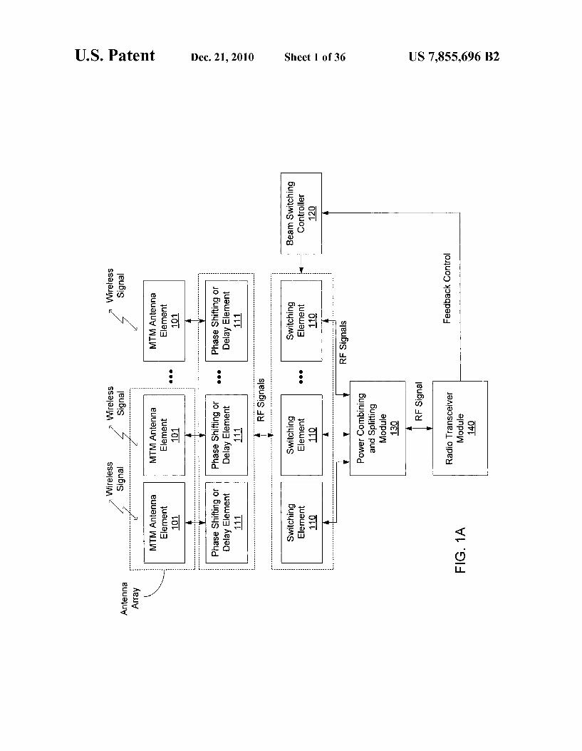
FIGS. 1A, 1B and 1C show examples of MTM antenna systems having MTM antenna arrays with radiation pattern shaping and beam Switching. These systems include antenna elements 101 that wirelessly transmit and receive radio sig nals and each antenna element 101 is configured to include a composite left and right handed (CRLH) metamaterial (MTM) structure. A radio transceiver module 140 is provided to be in communication with the antenna elements 101 to receive a radio signal from or to transmit a radio signal to the antenna elements 101. A power combining and splitting mod ule 130 is connected in signal paths between the radio trans ceiver module 140 and the antenna elements to split radio power of a radio signal directed from the radio transceiver module to the antenna elements and to combine power of radio signals directed from the antenna elements 101 to the radio transceiver module 140. Switching elements 110 are connected in signal paths between the power combining and splitting module 130 and the antenna elements 101 and each switching element 110 is operated to activate or deactivate at least one antenna element 101 in response to a Switching control signal from a beam switching controller 120. The beam switching controller 120 is in communication with the switching elements 110 to produce the switching control signal to control each Switching element 110 to activate at least one subset of the antenna elements 101 to receive or transmit a radio signal. Each Switching element 110 can be used to activate or deactivate the signal path between a single antenna element 101 and the power combining and splitting module 130 as shown in FIG. 1B. Alternatively, each switch ing element 110 can be used to activate or deactivate the signal path between two or more antenna elements 101 and the power combining and splitting module 130 as shown in FIG. 1C.

US 7,855,696 B2 7
Phase shifting elements or delay lines 111 are also pro vided in signal paths between the antenna elements 101 and power combining and splitting module 130 to control a radia tion pattern produced by each Subset of the antenna elements 101 activated by the switching elements 110. In this example, the phase shifting elements or delay lines 111 are in the signal paths between the antenna elements 101 and the switching elements 110. This control of the relative phase or delay between two or more adjacent antenna elements 101 can be combined with control over the amplitudes of the signals associated with the antenna elements to control the radiation pattern of each subset of the antenna elements 101. The antenna elements in one Subset can be adjacent antenna ele ments as an antenna array. When different Subsets are acti vated, the system has multiple antenna arrays. Such a system can be operated to activate one Subset of antenna elements 101 at a time or two or more subsets of antenna elements 101 at the same time. The beam switching controller 120 can be pre-pro
grammed with selected Switching configurations for the Switching elements 101. As an option, a feedback control can be provided to use the beam switching controller 120 to control the Switching elements 110 based on the signal qual ity of the received signal by the antenna elements 101. The radio transceiver module 140 includes a digital signal proces Sor that can be configured to process a received radio signal from the antenna elements 101 to evaluate a signal perfor mance parameter. The signal performance parameter is then used to produce a feedback control signal based on the signal performance parameter to control the beam Switching con troller 120 which in turn reacts to the feedback control signal to control a switching status of the switching elements 101 so that the evaluated signal performance in the received signal is improved. The packet error rate and the relative signal strength intensity, for example, can be used to evaluate the signal quality of the signal received by the antenna elements 101. As another option, the beam switching control 120 can be
configured to execute through the following operation modes of a scanning mode, a locked mode, a re-scanning mode, and a MIMO (multiple input multiple output) mode when con Verging toward the optimal beam pattern Suitable for commu nication environment at a specific location and time. The scanning mode is the initialization process where wider beams are used first to narrow down the directions of the strong paths before transitioning to narrower beams. Multiple directions may exhibit the same signal strength. These pat terns are stamped with client information and time before being logged in memory. In the locked mode, the Switching configuration that exhibits the best signal quality (e.g., the highest signal strength) is used to transmit and receive sig nals. If the link starts showing lower signal quality perfor mance, the re-scanning mode is triggered and the beam Switching controller 120 exits the locked mode and changes the switching configuration of the switching elements 110 to other Switching configurations, e.g., the pre-selected Switch ing configurations for certain beam patterns logged in memory. If none of these pre-selected Switching configura tions produces the satisfactory signal quality, the system then initiates the MIMO mode to find the directions of strong multipath links and then lock the MIMO multiple antenna patterns to these directions. Hence, multiple subsets of the antennas are operating simultaneously and each connected to the MIMO transceiver.
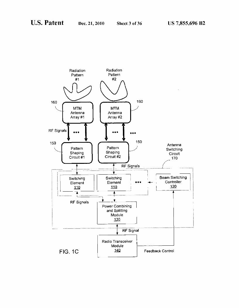
FIG. 1C shows another example of an MTM antenna sys tem having MTM antenna arrays with radiation pattern shap ing and beam switching. Each MTM antenna array 160
10
15
25
30
35
40
45
50
55
60
65
8 includes two or more antenna elements 101 and is connected to a pattern shaping circuit 150 designated to that array 160. Different antenna arrays 160 have different pattern shaping circuits 150. Each pattern shaping circuit 150 is used to sup ply a radiation transmission signal to a respective antenna array 160 and to produce and direct replicas of the radiation transmission signal with selected phases and amplitudes to the antenna elements 101 in the antenna array 160, respec tively, to generate a respective radiation transmission pattern associated with the antenna array 160.
For example, each pattern shaping circuit 150 controls the phase values and amplitudes of the signals to the antenna elements 101 in that array 150 to create a particular radiation pattern to have increased gain in certain directions. The pat tern shaping circuit 150 can, for example, include phase shift ing or delay elements 111 shown in FIGS. 1A and 1B. In this example, one Switching element 110 is connected to only one designated pattern shaping circuit 150 and different pattern shaping circuits 150 are connected to different switching elements 110. The switching elements, the beam switching controller 120 and the power combining and splitting module 130 collectively forman antenna switching circuit 170 that is coupled to the pattern shaping circuits 150 to supply the radiation transmission signal to at least one pattern shaping circuit 150 and configured to selectively direct the radiation transmission signal to at least one of the antenna arrays at a time to transmit the radiation transmission signal. Exemplary implementations of this antenna switching circuit 170 are described in this specification.
In FIG. 1C, the antenna switching circuit 170 is shown to receive a feedback control from the radio transceiver module 140. This feedback control can be a dynamic signal that varies in time due to changing signal conditions. The digital signal processor in the radio transceiver module 140 can monitor the signal conditions and inform the antenna Switching circuit 170 of the changing signal conditions and the control logic of the antenna Switching circuit 170 can adjust the beam forming pattern and beam Switching to dynamically improve the antenna system performance. In operation, the antenna switching circuit 170 activates at least one subset or antenna array of the antenna elements at a time to generate the radia tion pattern associated with the at least one Subset. The acti Vation is Switched among the Subsets as time passes based on a predetermined or adaptive control logic. The MTM antenna systems described in this application
can be implemented in ways that provide significant advan tages over other antenna systems in terms of size and perfor mance. Due to the current distribution in the MTM antenna structure, these antenna elements can be closely spaced with minimal interaction between adjacent antenna elements. This feature can be used to obtain compact antenna arrays with a desired radiation pattern. Examples of some MTM antenna structures that can be used to implement the present antenna systems are described in U.S. patent application Ser. No. 11/741,674 entitled “Antennas, Devices, and Systems Based on Metamaterial Structures, filed on Apr. 27, 2007, and U.S. patent application Ser. No. 1 1/844,982 entitled “Antennas Based on Metamaterial Structures, filed on Aug. 24, 2007, which are incorporated by reference as part of the specifica tion of this application. An MTM antenna or transmission line can be treated as a
MTM Structure with one or more MTM unit cells. The equivalent circuit for each MTM unit cell has a right-handed (RH) series inductance LR, a shunt capacitance CR and a left-handed (LH) series capacitance CL, and a shunt induc tance LL. The shunt inductance LL and the series capacitance CL are structured and connected to provide the left handed

US 7,855,696 B2 9
properties to the unit cell. This CRLHTL can be implemented by using distributed circuit elements, lumped circuit elements or a combination of both. Each unit cell is smaller than W10 where w is the wavelength of the electromagnetic signal that is transmitted in the CRLHTL or antenna. A pure LH material follows the left hand rule for the vector
trio (E.H.B) and the phase velocity direction is opposite to the signal energy propagation. Both the permittivity and perme ability of the LH material are negative. A CRLH Metamate rial can exhibit both left hand and right hand electromagnetic modes of propagation depending on the regime or frequency of operation. Under certain circumstances, a CRLH metama terial can exhibit a non-zero group Velocity when the wavevector of a signal is Zero. This situation occurs when both left hand and right hand modes are balanced. In an unbalanced mode, there is a bandgap in which electromag netic wave propagation is forbidden. In the balanced case, the dispersion curve does not show any discontinuity at the tran sition point of the propagation constant B(c))=0 between the Left and Right handed modes, where the guided wavelength is infinite 27t/IB|->oo while the group velocity is positive:
do "g - 4 go 0
This state corresponds to the Zeroth Order mode m=0 in a Transmission Line (TL) implementation in the LH handed region. The CRHL structure supports a fine spectrum of low frequencies with a dispersion relation that follows the nega tive B parabolic region which allows a physically small device to be built that is electromagnetically large with unique capa bilities in manipulating and controlling near-field radiation patterns. When this TL is used as a Zeroth Order Resonator (ZOR), it allows a constant amplitude and phase resonance across the entire resonator. The ZOR mode can be used to build MTM-based power combiners and splitters or dividers, directional couplers, matching networks, and leaky wave antennas. Examples of MTM-based power combiners and dividers are described below.
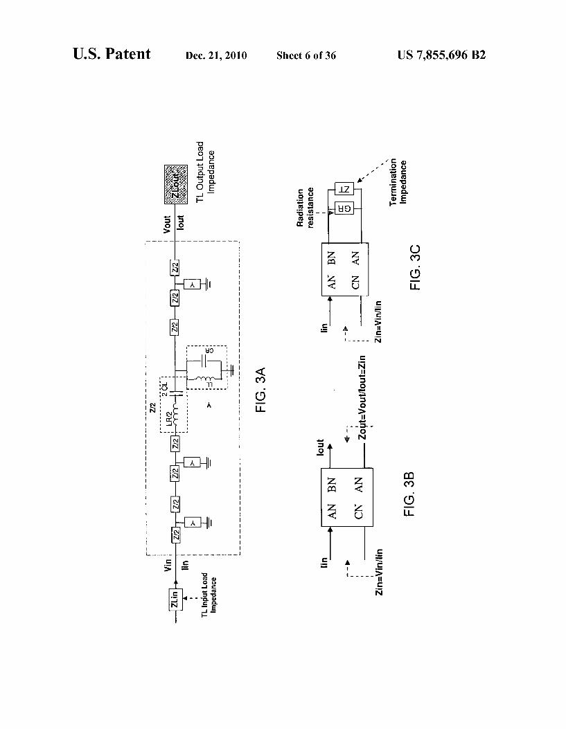
In RHTL resonators, the resonance frequency corresponds to electrical lengths 0, Bl-mt (m=1,2,3,...), where 1 is the length of the TL. The TL length should be long to reach low and wider spectrum of resonant frequencies. The operat ing frequencies of a pure LH material are at low frequencies. A CRLH metamaterial structure is very different from RH and LH materials and can be used to reach both high and low spectral regions of the RF spectral ranges of RH and LH materials. In the CRLH case 0-fl-mat, where 1 is the length of the CRLH TL and the parameter m=0, +1, +2, t3, . . . , too. FIG. 2 provides an example of a 1D CRLH material Trans
mission Line (TL) based on four unit cells. The four patches are placed above a dielectric substrate with centered vias connected to the ground electrode. FIG. 2A shows an equiva lent network circuit analogy of the device in FIG.2. The ZLin' and ZLout' corresponding to the input and output load imped ances respectively and are due to the TL couplings at each end. This is an example of a printed 2-layer structure. FIG. 2C shows the equivalent circuit for an antenna with four MTM unit cells as shown in FIG. 2D. The impedance labeled “GR’ represents the radiation resistance of the antenna. In FIGS. 2A-2C, the correspondences between FIG. 2 and FIG. 2A are illustrated, where the Right-Handed (RH) series inductance LR and shunt capacitor CR are due to the dielectric being sandwiched between the patch and the ground plane, the
10
15
25
30
35
40
45
50
55
60
65
10 series Left-Handed (LH) capacitance CL is due to the pres ence of two adjacent patches, and the via induces the shunt LH inductance LL.
The individual internal cell has two resonances ()s and cost corresponding to the series impedance Z and shunt admittance Y. Their values are given by the following relation:
1 1 1 VLRCR
(1)
1 here, Z = icoLR where, I(t) ico LL and Y = icoCR+ icoCL
The two input/output edge cells in FIG. 2A do not include part of the CL capacitor since it represents the capacitance between two adjacent MTM cells, which are missing at these input/output ports. The absence of a CL portion at the edge cells prevents ()s frequency from resonating. Therefore, only cost appears as an n=0 resonance frequency.
In order to simplify the computational analysis, we include part of the ZLin' and ZLout' series capacitor to compensate for the missing CL portion as seen in FIG. 3A. Under this condition, all N cells have identical parameters. FIG.2B and FIG.3B provide the 2-ports network matrix of
FIG. 2A and FIG. 3A, respectively, without the load imped ances, and FIG. 2C and FIG. 3C provide the analogous antenna circuit when the TL design is used as an antenna. In matrix notations, FIG. 3B represents the relation given by:
Wirt AN BNY Voitt (2) (E)=(C, "C)
where AN=DN because the CRLH circuit in FIG. 3A is symmetric when viewed from Vin and Vout ends. The imped ance “GR’ is the structure corresponding to radiation resis tance and ZT is the termination impedance. ZT is basically the desired termination of the structure in FIG. 2B with an additional 2CL series capacitor. The same goes for ZLin' and ZLout', in other terms:
3 ZLin' = ZLin + icoCL ZLout = ZLin + icoCL (3)
2 ZT = ZT---
icoCL
Since the radiation resistance “GR’ is derived by either building the antenna or simulating it with HFSS, it is difficult to work with the antenna structure to optimize the design. Hence, it is preferable to adopt the TL approach and then simulate its corresponding antennas with various termina tions ZT. The notations in Eq. (1) also hold for the circuit in FIG. 2A with the modified values AN', BN', and CN' which reflect the missing CL portion at the two edge cells. The frequency bands are determined from the dispersion
equation derived by letting the NCRLH cell structure reso nates with nTC propagation phase length, where n=0, t1, +2, ... +N. Here, each of the NCRLH cells is represented by Z and Y in Eq.(1), which is different from the structure shown in FIG. 2A, where CL is missing from end cells. Hence, one

US 7,855,696 B2 11
might expect that the resonances associated with these two structures are different. However, extensive calculations show that all resonances are the same except for n=0, where both cost and cost resonate in the first structure and only cost resonates in the second one (FIG. 2A). The positive phase offsets (no-0) correspond to RH region resonances and the negative values (n0) are associated with LH region reso aCCS.
The dispersion relation of N identical cells with the Z and Y parameters, which are defined in Eq. (1), is given by the following relation:
NBp = cos' (Aw). = |A| < 1 = 0 < x = -ZY is 4WN (4) where
AN = 1 at even resonances n = 2n e {0, 2, 4, .2xin') and
AN = -1 at odd resonances n = 2n + 1 e {1, 3, ... (2x Int:)- 1)}
where, Z and Y are given in Eq.(1), AN is derived from either the linear cascade of N identical CRLH circuit or the one
shown in FIG. 3A, and p is the cell size. Odd n=(2m+1) and even n=2m resonances are associated with AN=-1 and AN=1, respectively. For AN' in FIG. 2A and FIG. 2B, due to the absence of CL at the end cells, the n=0 mode resonates at (no-cost only and not at both ()s and cost regardless of the number of cells. Higher frequencies are given by the follow ing equation for the different values of specified in Table 1:
For n > 0, (5)
2 2 2
(OSH (OSE 2 coin + (or + Moi cush + Co. + Maoi
(O. F 2 2
Table 1 provides X values for N=1, 2, 3, and 4. It should be noted that the higher resonances n>0 are the same regardless if the full CL is present at the edge cells (FIG. 3A) or absent (FIG. 2A). Furthermore, resonances close to n=0 have small X values (near X lower bound 0), whereas higher resonances tend to reach X upper bound 4 as stated in Eq. (4).
TABLE 1.
Resonances for N = 1, 2, 3 and 4 cells.
NXModes n = 0 n = 1 n = 2 n = 3
N = 1 X.1.0) = 0: (Do = (0sri N = 2 X20) = 0: (Do = (ost X21) = 2 N = 3 X(30) 0: (Do = (Ostf X(31) 1 X(3.2) 3 N = 4 XC40) = 0: (Do = Gosty X.4,1) = 2 - W2 X(4,2) = 2
An illustration of the dispersion curve B as a function or omega is provided in FIGS. 4A and 4B for the cos(t)s. (balanced) and coszcos (unbalanced) cases respectively. In the latter case, there is a frequency gap between min (cos, (Ost) and max (cose, (Dstl). The limiting frequencies (), and co, values are given by the same resonance equations in Eq. (5) with X reaching its upper bound X-4 as stated in the following equations:
10
15
25
30
35
40
45
50
55
60
65
2 2 2 2 2 22 (6)
(of. = cost + (ost + 4(of (est. to ties) co, co -— - (- , ) - ushese
2 2 2 2 2 22 2 (USH + COSE +4(of (us + cost + 4cof 2 2 (ona — —- — —) - (OSH (OSE
FIGS. 4A and 4B provide examples of the resonance posi tion along the beta curves. FIG. 4A illustrates the balanced case where LR CL=LL CR, and FIG. 4B shows the unbal anced case with the gap between LH and RH regions.
In the RH region (no-0) the structure size l=Np, where p is the cell size, increases with decreasing frequencies. In con trast, in the LH region, lower frequencies are reached with smaller values of Np, hence size reduction. The B curves provide some indication of the bandwidth around these reso nances. For instance, LH resonances suffer from narrow bandwidth because the B curves are almost flat. In the RH region bandwidth should be higher because the B curves are steeper, or in other terms:
7 COND1:1 BB condition = (7)
dcores
d(AN) -- do << 1 near (t) = (opes = (u0, (t)+1.
(1 - AN2)
d d
o... = E = - do << 1 with p = do
2p x(l 3) 4 aS
d 2c) in 2 2 cell size and A = "P1-PESH dcores coi coln
where, X is given in Eq. (4) and () is defined in Eq.(1). From the dispersion relation in Eq. (4) resonances occur when |AN=1, which leads to a zero denominator in the 1 BB condition (COND1) of Eq. (7). As a reminder, AN is the first transmission matrix entry of the N identical cells (FIG. 3A and FIG. 3B). The calculation shows that COND1 is indeed independent of N and given by the second equation in Eq. (7). It is the values of the numerator and X at resonances, which are defined in Table 1, that define the slope of the dispersion curves, and hence possible bandwidth. Targeted structures are at most Np-w/40 in size with bandwidth exceeding 4%. For structures with small cell sizes p, Eq. (7) clearly indicates that high () values satisfy COND1, i.e. low CR and LR values since for n-0 resonances happens at X values near 4 in Table 1, in other terms (1-X/4->0). As previously indicated, once the dispersion curve slopes
have steep values, then the next step is to identify suitable matching. Ideal matching impedances have fixed values and do not require large matching network footprints. Here, the word “matching impedance” refers to feed lines and termi nation in case of a single side feed such as antennas. In order to analyze input/output matching network, Zinand Zout need to be computed for the TL circuit in FIG. 3B. Since the network in FIG. 3A is symmetric, it is straightforward to demonstrate the Zin-Zout. It can be demonstrated that Zin is independent of N as indicated in the equation below:
US 7,855,696 B2 13
(8)
(1 i), which has only positive real values
The reason that B1/C1 is greater than Zero is due to the condition of IANs 1 in Eq. (4) which leads to the following impedance condition:
The 2". BB condition is for Zin to slightly vary with fre quency near resonances in order to maintain constant match ing. Remember that the real matching Zin' includes a portion of the CL Series capacitance as stated in Eq. (3).
dZin do
(9) COND2:2". BB condition near resonances, << 1 28 as
Different from the transmission line example in FIG. 2 and FIG. 2B, antenna designs have an open-ended side with an infinite impedance which typically poorly matches the struc ture edge impedance. The capacitance termination is given by the equation below:
(10) ZT = CN which depends on N and is purely imaginary
Since LH resonances are typically narrower than the RH ones, selected matching values are closer to the ones derived in the n-O than the no-0.
In order to increase the bandwidth of LH resonances, the shunt capacitor CR can be reduced. This reduction leads to higher () values of steeper beta curves as explained in Eq. (7). There are various ways to decrease CR, including: 1) increasing Substrate thickness, 2) reducing the top cell patch area, or 3) reducing the ground electrode under the top cell patch. In designing the devices, these three methods may be combined to produce a desired design.
FIG. 5A illustrates one example of a truncated ground electrode (GND) in a 4-cell transmission line where the GND has a dimension less than the top patch along one direction underneath the top cell patch. The ground conductive layer includes a strip line 510 that is connected to the conductive via connectors of at least a portion of the unit cells and passes through underneath the conductive patches of the portion of the unit cells. The strip line 510 has a width less than a dimension of the conductive path of each unit cell. The use of truncated GND can be more practical than other methods to implement in commercial devices where the substrate thick ness is Small and the top patch area cannot be reduced because of lower antenna efficiency. When the bottom GND is trun cated, another inductor Lp (FIG. 5B) appears from the met allization strip that connects the vias to the main GND as illustrated in FIG. 5A. FIG.5C shows a 4-cell antenna based on the structure in FIG. 5A.
FIGS. 6A and 6B show another example of a truncated GND design. In this example, the ground conductive layer includes a common ground conductive area 601 and strip
10
15
25
30
35
40
45
50
55
60
65
14 lines 610 that are connected to the common ground conduc tive area 601 at first distal ends of the strip lines 610 and having second distal ends of the strip lines 610 connected to conductive via connectors of at least a portion of the unit cells underneath the conductive patches of the portion o the unit cells. The strip line 610 has a width less than a dimension of the conductive path of each unit cell. The equations for truncated GND can be derived. The
resonances follow the same equation as in Eq.(5) and Table 1 as explained below:
Approach 1 (FIGS.5A and 5B): Resonances: same as in Eqs (1), (5) and (6) and Table 1
after replacing LR by LR+Lp CR becomes very small Furthermore, for Inlz0, each mode has two resonances
corresponding to (1) coin for LR being replaced by LR+Lp (2) coin for LR being replaced by LR--Lp/N where N is
the number of cells The impedance equation becomes:
BN 11 Zin' = - (11) CN
B1 C1 Z?. + p \, (1 - Y - p)
= -1 - h (1–4 . it where = -YZ and
= -YZp
where Zp-coLp and Z, Y are defined in Eq. (2). From the impedance equation in Eq. (11), it can be seen that the two resonances () and (o' have low and high impedance respectively. Hence, it is easy to tune near the () resonance in most cases.
Approach 2 (FIGS. 6A and 6B): Resonances: same as in Eq. (1), (5), and (6) and Table 1
after replacing LL by LL+Lp CR becomes very small
In the second approach, the combined shunt induction (LL Lp) increases while the shunt capacitor decreases, which leads to lower LH frequencies. Due to the current distribution in the MTM structure, the
MTM antennas can be closely spaced with minimal interac tion between them Caloz and Itoh, “Electromagnetic Metamaterials: Transmission Line Theory and Microwave Applications,” John Wiley & Sons (2006) pp. 172-177). The close spacing makes radiation pattern shaping more tractable than otherwise.
Referring back to FIG. 1, the pattern shaping circuit splits the RF signal into different antenna feed signals with required amplitude and phase to create the desired radiation pattern. Many different techniques can be used to shape the radiation pattern, including techniques based on phase combining, a Wilkinson power combiner/divider, phase combining using Zero-degree metamaterial transmission line, a metamaterial coupler, and an Electromagnetic Band Gap (EBG) structure.
Referring back to FIG. 1, the antenna switching circuit feeds the RF signal from the wireless radio to one or more pattern shaping circuits based on the antenna control logic. This control logic takes into consideration the signal strength from the communication link. Examples of the antenna switching circuit include: 1) conventional RF switch IC, 2)

US 7,855,696 B2 15
conventional radial divider/combiner terminated with switch ing devices such as diodes and Switches, and 3) metamaterial radial combiner/divider terminated with switching devices Such as diodes and Switches.
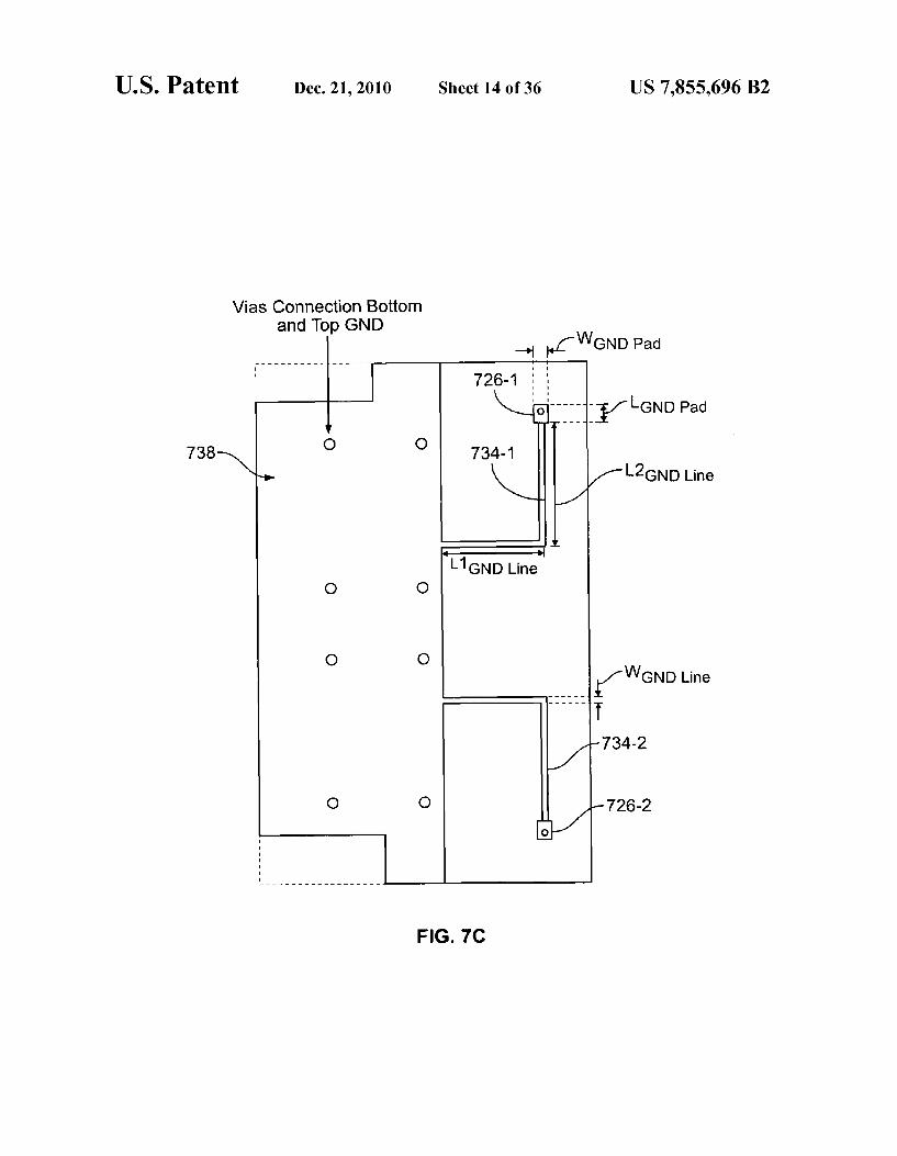
FIGS. 7A-7D show an example of a 2-antenna MTM array that can be used to implement the antenna elements of the present systems. The top and bottom layers can be formed in the top and bottom metallization layers on the FR4 substrate shown in FIG. 7E. The dielectric substrate on which the antenna elements are
formed includes two different conductive layers. The first conductive layer is the top layer supported by the dielectric Substrate and is patterned to include a first (top) main ground electrode 742 that is patterned to include separate co-planar waveguides 710-1 and 710-2 to guide and transmit RF sig nals. The cell conductive patches 722-1 and 722-2 are sepa rated from the first main ground electrode 742 and is in the first layer. Cell conductive feed lines 718-1 and 718-2 are formed on the first layer so that each cell conductive feed line has a first end connected to a respective co-planar waveguide and a second end electromagnetically coupled via capacitive coupling to a respective cell conductive patch to carry a respective RF signal between the respective co-planar waveguide and the respective cell conductive patch. In each cell, a cell conductive launch pad 714-1 or 714-2 is formed in the first layer and is located between each cell conductive patch and a respective conductive feed line with a narrow gap with the cell conductive patch to allow for electromagneti cally coupling to the cell conductive patch. The launch pad is connected to the second end of the respective conductive feed line. The second (bottom) conductive layer supported by the
dielectric substrate is separate from and parallel to the first (top) conductive layer. This conductive layer is patterned to include a second main ground electrode 738 in a footprint projected to the second conductive layer by the first ground electrode 742. Cell ground conductive pads 726-1 and 726-2 are respectively located in footprints projected to the second conductive layer by the cell conductive patches 722-1 and 722-2. Ground conductive lines 734-1 and 734-2 connect the cell ground conductive pads 726-1 and 726-2 to the second main ground electrode 738, respectively. In this example, the cell ground conductive pad has a dimension less than a dimension of a respective cell conductive patch in a truncated ground design.
Cell conductive via connectors 730-1 and 730-2 are formed in the Substrate and each cell conductive via connection con nects a cell conductive patch and the corresponding cell ground pad. Multiple ground via connectors are formed in the substrate to connect the first main ground electrode 742 in the first conductive layer and the second main ground electrode 738 in the second conductive layer. In this example, each cell conductive patch, the Substrate, a respective cell conductive via connector and the cell ground conductive pad, a respective co-planar waveguide, and a respective electromagnetically coupled conductive feed line are structured to form a com posite left and right handed (CRLH) metamaterial structure as one antenna element. The 2 antenna elements can be made to be identical in structure but are oriented in opposite direc tions (as shown) to minimize coupling and maximize the diversity gain. The different sectional views of the antennas are shown in
FIGS. 7B, 7C, and 7D. Each 5092 co-planar waveguide (CPW) line is denoted by reference numeral 710. Each antenna comprises an MTM cell, a launchpad 714 and a feed line 718, where the MTM cell is connected to the 5092 CPW line 710 via the launch pad 714 and the feed line 718. The MTM cell comprises a cell patch 722 which has an rectangu lar shape in this example, a ground (GND) pad 726, a via 730 which has a cylindrical shape and connects the cell patch 722
10
15
25
30
35
40
45
50
55
60
65
16 with the ground (GND) pad 726, and a ground (GND) line 734 which connects the GND pad 726, hence the MTM cell, with a main ground (GND) 738. The cell patch 722, launch pad 714 and feed line 718 are located on the top layer. There is a gap between the launch pad 714 and the cell patch 722. The GND pad 726 in this example has a small square shape and connects the bottom part of the via 730 to the GND line 734. The GND pad 726 and the GND line 734 are located on the bottom layer. The CPW feed line is surrounded by a top ground (GND) 742. The antennas were simulated using HFSS EM simulation
Software. In addition, Some of the designs were fabricated and characterized by measurements.
In one implementation, the substrate is FR4 with dielectric constant 6–4.4 and with width=64 mm, length=38 mm, and thickness=1.6 mm. The GND size is 64x30mm. The cell size is 3x6.2 mm and is located at 8 mm away from the top GND 742. At -10 dB the bands are at 2.38-2.72 GHz.
Specific geometrical shapes and dimensions of the anten nas are employed in this example. It should be understood that various other antenna variations can also be used to comply with other Printed Circuit Board (PCB) implementation fac tors. Examples of several variations are listed below The launch pad 714 can have different geometrical shapes
Such as but not limited to rectangular, spiral (circular, oval, rectangular, and other shapes), or meander.
The cell patch 722 can have different geometrical shapes Such as but not limited to rectangular, spiral (circular, oval, rectangular, and other shapes), or meander
The gap between the launchpad 714 and the cell patch 722 can take different forms such as but not limited to straight line, curved, L-shape, meander, ZigZag, or dis continued line.
The GND line 734 that connects the MTM cell to the GND can be located on the top or bottom layer.
Antennas can be placed few millimeters above the sub Strate.
Additional MTM cells may be cascaded in series with the first cell creating a multi-cell 1D structure.
Additional MTM cells may be cascaded in an orthogonal direction generating a 2D structure.
Antennas can be designed to Support single or multi-bands.
As discussed earlier, the antenna resonances are affected by the presence of the left handed mode. When one of the fol lowing operations is performed, the lowest resonance in both the impedance and return loss disappears: The gap between the launchpad 714 and the cell patch 722
is closed. This corresponds to an inductively loaded monopole antenna.
The GND line 734 connecting the MTM cell to GND is removed.
The GND line 734 is removed and the gap is closed. This corresponds to a printed monopole resonance.
The left handed mode helps excite and better match the lowest resonance as well as improves the matching of higher reso aCCS.
FIGS. 8A and 8B show two examples of pattern shaping using phase-combining of signals. In both examples, two MTMantenna elements 801 and 802 are connected to receive replicas of the common RF signal. A 3-port RF splitter is provided to feed the RF signal to the two antenna elements 801 and 802. This RF splitter includes a main CPW feed line 800 that receives the RF signal generated by the radio trans ceiver module, a branch point 814, two CPW branch feed lines 810 and 820. The terminals 811 and 812 of the two branch feed lines 810 and 820 are respectively connected to the two antenna elements 801 and 802.

US 7,855,696 B2 17
The antenna system in FIG. 8A is configured to have a phase offset of 0 degree between the two branch feed lines 810 and 802. Therefore, the two MTM antennas 801 and 802 are fed in phase and this equal phase condition creates a dipole-like radiation pattern in the YZ plane and an omni directional radiation pattern in the XY plane. FIG. 8C shows the radiation pattern.
The antenna system in FIG. 8B is configured to have dif ferent lengths for the two branch CPW feedlines 810 and 820 with a phase offset of 90 degrees. Therefore, the two antennas 801 and 802 are fed 90 degrees out of phase with respect to each other. Referring to FIG.8D, this out of phase condition creates a directional pattern with high gain in the -X direction and very good rejection in the +X direction. In such antenna systems, the radiated patterns are determined by the phase offset of the signals and the distance between the two anten nas 801 and 802. The phase offset of the radiated signals between the two antennas 801 and 802 can be varied by changing the relative length between the two branch feed lines 810 and 820 connected to respective antennas. Specifi cally, as shown in top figures in FIGS. 8A and 8B, the phase offset is determined by the difference between the length of the first feed line 810 connecting the first antenna input point 811 with the branch point 814 and the length of the second feed line 820 connecting the second antenna input point 812 with the branch point 814. The coupling between the two antennas 801 and 802 can be difficult to control in this phase combining scheme due to the connected paths inherent in the design. Thus, the two antennas together act as a single antenna.
FIGS. 9A and 9B show an example of pattern shaping circuit using a Wilkinson power divider. Examples of Wilkin son power dividers can be found in, e.g., pages 318-323 in Pozar, “Microwave Engineering.” John Wiley & Sons (2005). FIG.9A shows a 3D view of the structure and FIG.9B shows the top view of the structure. The Wilkinson power divider 910 is designed so as to generate two replica signals of equal amplitude and phase of a common RF signal received by the main CPW feed line 901. Two branch CPW feed lines 911 and 912 are connected to the Wilkinson divider output point 914 to receive the two signals, respectively, and to feed the two signals to the two MTM antenna elements. The two feed lines 911 and 912 are minimally coupled in this case owing to the design of the Wilkinson power divider 910. The phase offset of the radiated signals is determined by the difference in length between the feedlines 911 and 912 from the Wilkinson divider output 914 to respective antenna input points, that is, the difference between the first length between the Wilkinson divider output 914 and the first antenna input point 918-1 and the second length between the Wilkinson divider output 914 and the second antenna input point 918-2. Using this phase offset, in conjunction with the distance between the two antennas, a variety of radiation patterns can be created. FIG.9C shows the measured radiation patterns in the XY.
XZ and YZ-planes for this example. The radiation pattern is shaped with the maximum gain of 1.7 dBi in the XY-plane at 0=140 degree and a rejection of greater than 10 dB in the XY-plane at 0=15 degree.
Shaping of the radiation pattern can be achieved by using a Zero degree CRLH transmission line (TL). The theory and analysis on the design of Zero degree CRLH transmission lines are summarized below. Examples of such CRLH trans mission lines are described in U.S. patent application Ser. No. 11/963,710 entitled “Power Combiners and Dividers Based on Composite Right and Left Handed Metamaterial Struc tures” and filed on Dec. 21, 2007, which is incorporated by reference as part of the specification of this application.
10
15
25
30
35
40
45
50
55
60
65
18 Referring back to FIGS. 4A and 4B as well as to Eq.(1), in
the unbalanced case where LCzLC, two different reso nant frequencies (), and () , exist and they can Support an infinite wavelength. At () and (), the group Velocity (v. do)/df) is zero and the phase velocity (V-co/f) is infinite. When the series and shunt resonances are equal, i.e. LCLC, the structure is balanced, and the resonant fre quencies coincide: (i) ()-().
For the balanced case, the phase response can be approxi mated by:
Nico C
pRH is - N2t fW LRCR N
pit as - – 27tfWLLCL
where N is the number of unit cells. The slope of the phase is given by:
N dipCRLH df
The characteristic impedance is given by:
ZCRLH - LR LL T W C T W C
The inductance and capacitance values can be selected and controlled to create a desired slope for a chosen frequency. In addition, the phase can be set to have a positive phase offset at DC. These two factors are used to provide the designs of multi-band and other MTM power combining and dividing Structures.
The following sections provide examples of determining MTM parameters of dual-band mode MTM structures. Simi lar techniques can be used to determine MTM parameters with three or more bands.
In a dual-band MTM structure, the signal frequencies f. f. for the two bands are first selected for two different phase values: (p at f and (p at f. Let N be the number of unit cells in the CRLHTL and Z, the characteristic impedance. The values for parameters L., C. L. and C can be calculated as:
Z RLH = LR LL CR CL

US 7,855,696 B2 19
In the unbalanced case, the propagation constant is given by:
2 LRC 1 (f f3 = S(co) (or R* 2LC, L*C,
-1 if (to < min(cuse, Cosh): LH range With s(a) =
+1 if () > max(cuse, Cosh). RH range
For the balanced case:
1 f3 = Cow LRCR -
Cow LLCL
ACRLHTL has a physical length of d with Nunit cells each having a length of p: d=N.p. The signal phase value is (p=-Bd. Therefore,
d) B = - and ----
p3 = (N. p)
It is possible to select two different phases (p and (p at two different frequencies f and f, respectively:
1 f3 = (1 WLR CR - - –
Cow LLCL 1
f32 = (2 WLR CR - - –. Co2 WLLCL
In comparison, a conventional RH microStrip transmission line exhibits the following dispersion relationship:
2it f3 = Bo + -n, n = 0, -1, -2, ... p
See, for example, the description on page 370 in Pozar, “Microwave Engineering, 3rd Edition John Wiley & Sons (2005), and page 623 in Collin, “Field Theory of Guided Waves.” Wiley-IEEE Press, 2nd Edition (Dec. 1, 1990).
Dual- and multi-band CRLH TL devices can be designed based on a matrix approach described in the referenced U.S. patent application Ser. No. 1 1/844,982. Under this matrix approach, each 1D CRLH transmission line includes N iden tical cells with shunt (L.C.) and series (LC) parameters. These five parameters determine the N resonant frequencies and phase curves, corresponding bandwidth, and input/output TL impedance variations around these resonances. The frequency bands are determined from the dispersion
equation derived by letting the NCRLH cell structure reso nates with nat propagation phase length, where n=0, t1, ... t(N-1). That means, a Zero and 271 phase resonances can be accomplished with N=3 CRLH cells. Furthermore, a tri-band power combiner and divider can be designed using N=5 CRLH cells where Zero, 271, and 47L cells are used to define SOaCS.
10
15
25
30
35
40
45
50
55
60
65
20 The n=0 mode resonates at () ()s and higher frequencies
are given by the following equation for the different values of M specified in Table 1:
For n > 0,
2 . .2 SH (OSE .
2 - coin + (or + Moi coiu + (or + Maoi 2 (O. F 2 2 - C
Table 2 provides M values for N=1, 2, 3, and 4.
TABLE 2
Resonances for N = 1, 2, 3 and 4 cells
NXModes n = 0 n = 1 n = 2 n = 3
N = 1 M = 0; Opo = (0s N = 2 M = 0; oo = (0s M = 2 N = 3 M = 0; oo = (0s M = 1 M = 3 N = 4 M = 0; coo = cost, M = 2 - V2 M = 2
FIG. 10 shows an example of the phase response of a CRLH TL which is a combination of the phase of the RH components and the phase of the LH components. Phase curves for CRLH, RH and LH transmission lines are shown. The CRLH phase curve approaches to the LHTL phase at low frequencies and approaches to the RHTL phase at high fre quencies. It should be noted that the CRLH phase curve crosses the Zero-phase axis with a frequency offset from Zero. This offset from zero frequency enables the CRLH curve to be engineered to intercept a desired pair of phases at any arbi trary pair of frequencies. The inductance and capacitance values of the LH and RH can be selected and controlled to create a desired slope with a positive offset at the Zero fre quency (DC). By way of example, FIG. 10 shows that the phase chosen at the first frequency f. is 0 degree and the phase chosen at the second frequency f. is -360 degrees. The two frequencies f and f, do not have a harmonic frequency rela tionship with each other. This feature can be used to comply with frequencies used in various standards such as the 2.4 GHz band and the 5.8 GHz in the Wi-Fi applications. A zero degree CRLH transmission line refers to a case in which the CRLH unit cell is configured to provide a phase offset of zero degree at an operating frequency. FIG.11A shows an example of a distributed MTM unit cell
structure that can be used in the design of the Zero degree CRLH transmission line. Various configurations for distrib uted MTM unit cells are possible and some examples are described and analyzed in Caloz and Itoh, “Electromagnetic Metamaterials: Transmission Line Theory and Microwave Applications. John Wiley & Sons (2006).
In FIG. 11A, the MTM unit cell includes a first set of connected electrode digits 1110 and a second set of connected electrode digits 1114. These two sets of electrode digits are separated without direct contact and are spatially interleaved to provide electromagnetic coupling with one another. A per pendicular stub electrode 1118 is connected to the first set of connected electrode digits 1110 and protrudes along a direc tion that is perpendicular to the electrode digits 1110 and 1110. The perpendicular stub electrode 1118 is connected to the ground electrode to effectuate the LH shunt inductor. In one example, various dimensions are specified as follows. The cell is designed for a 1.6 mm thick FR4 substrate. The series capacitance comprises an interdigital capacitor that has 12 digits, each digit with 5 mil width. The spacing between
US 7,855,696 B2 21
the digits is 5 mil. The length of each digit is 5.9 mm. The shunt inductor is a shorted stub of length 7.5 mm and width 1.4 mm. The stub 1118 is shorted to the ground using a via with 10 mill diameter.
FIG. 11B shows an example of a 3-port CRLH transmis sion line power divider and combiner based on the distributed CRLH unit cell in FIG. 11A. This 3-port CRLHTL power divider and combiner is shown to include two unit cells in FIG. 11A with perpendicular shorted stub electrodes 1118. Two branch feedlines 1121 and 1122 are connected to the two MTM cells, respectively, to provide two branch ports 2 and 3. The distributed CRLH transmission line can be structured as a Zero degree transmission line to form a Zeroth order power combiner and divider with the structure in FIG. 11B.
FIG. 11C shows an example antenna system that uses a 4-branch zero degree CRLH transmission line for shaping the radiation pattern emitted by two adjacent MTM antenna ele ments of four MTM antenna elements. In this example, the four MTM antenna elements 1-4 are formed by four MTM unit cells are connected in series with four feed lines to form two sets of 2-antenna MTM arrays where the adjacent antenna elements 1 and 2 are located close to each other on one edge of the circuit board as the first set and the adjacent antenna elements 3 and 4 are located close to each other on another edge of the circuit board as the second set. The 4-branch Zero degree CRLH transmission line is based on the distributed MTM unit cell design in FIGS. 11A and 11B. The signal input from the input point 1122 of the TL is split at the four output points 1124-1 through 1124-4. The TL is designed so that the phase offset between two neighboring split signals at 1124-1 and 1124-2 is Zero degree and the phase offset between two neighboring split signals at 1124-3 and 1124-4 is Zero degree. The radiation patterns can be changed by changing the distances among antennas, and the differ ences in length among the feed lines and thus the phase offsets. Each feed line connects one of the output points 1124-1 through 1124-4 with the corresponding antenna. These output points are independent due to the design of the Zero-degree CRLHTL, and thus the individual MTM anten nas can be treated independently. Therefore, performance of the pattern shaping device by use of the Zero degree CRLH transmission line does not depend on the number of antennas connected.
FIG. 11D shows the measured radiation patterns in the XY. XZ and YZ planes for the case of using two sets of the 2-antenna MTMarrays (i.e. total of four MTM antennas) with the Zero degree CRLH transmission lines. The radiation pat tern is shaped with the maximum gain of 2.9 dBi in the XY-plane at 0–210 degree and a rejection of greater than 10 dB in the XY-plane at 0–90 degree.
Shaping of the radiation pattern can be achieved by using an MTM directional coupler. The theory and analysis on the design of MTM couplers are described in U.S. Provisional Patent Application Ser. No. 61/016,392 entitled “Advanced Metamaterial Multi-Antenna Subsystems.” filed on Dec. 21, 2007, which is incorporated by reference as part of the speci fication of this application, and Summarized below. The technical features associated with the MTM coupler
can be used to decouple multiple coupled antennas using a four-port microwave directional coupler as shown in FIG. 12. In this figure, the coupling magnitude and phase for path 1 through path 4 are represented as Cn and On, respectively, where n=1, 2, 3, 4. In the ideal situation where
10
15
25
30
35
40
45
50
55
60
65
22 the Zero coupling between two input ports can be obtained. Thus, the MTM coupler can be configured to increase isola tion between different signal ports and restore orthogonality between multi-path signals at the output.
In the example shown in FIG. 13A, a directional MTM coupler is used to offset the antenna feed signals to create an orthogonal radiation pattern set at the two input ports for antennas. The MTM directional coupler has four input/output ports, where in this example port 1 and port 2 are used for RF inputs and the two outputs are connected to the 2-antenna MTM array. In this example, the dimensions of various parts of the MTM coupler are specified as follows. The total CPW feed line length including two rectangular CPW sections and two CPW bends are 0.83 mmx4.155 mm with 0.15 mm slot width. This CPW feed line has a characteristic impedance of around 5092. The connection side of the CPW bend has 0.83 mm width. The coupling portion of this coupler is realized by a CPW MTM coupled line where two CPW MTM transmis sion lines are placed in parallel to each other with a coupling capacitor Cm connecting in between. The total length of the one cell CPW MTM coupled line in this example is 4.4 mm and the gap between two CPW MTM transmission lines is 1 mm. The chip capacitor of 0.4 pF (C) is used here to enhance the coupling between two CPW MTM transmission lines. Each CPW MTM transmission line comprises two segments of CPW lines, a capacitor pads, two series capacitors (2*C) and one shorted stub. All the CPW segments are identical in this MTM coupler design and each section is 0.83 mmx1.5 mm. Two CPW sections on one side are connected by two series capacitors of 2C. The capacitor pad between the two CPW segments is a metal base to mount the series capacitors on. In this example C, is realized by using a chip capacitor of 1.5 pF. The spacing between the CPW segment and the capacitor pad is 0.4 mm. The size of the capacitor pad is 0.6 mmx0.8 mm. The shorted stub is implemented by using a CPW Stub where one side of the CPW Stub is attached to the capacitor pad and the other side is connected directly to the CPW ground. The CPW stub is 0.15mmx2.5 mm with 0.225 mm slot width in this example.
FIG. 13B shows the measured radiation patterns of the 2-antenna MTM array with the MTM coupler. Here, the sig nal patterns at port 1 and port 2 are created to be orthogonal to each other based on the decoupling scheme explained earlier. Generally, the physical size of a conventional RH coupler is determined by the operating frequency and the phase 01. As a result, the circuit size becomes too large to fit in certain wireless communication systems. In contrast, the present technique by use of the MTM coupler provides size reduction owing to its design, and thus is useful in these size-limited applications.
In another radiation shaping technique, a single negative metamaterial (SNG) is used between two MTM antennas to direct the radiation patterns in certain directions. The SNG materials, which are also known as electromagnetic bandgap (EBG) structures in microwave regimes, are type of materials that are characterized by (exu)<0 in their effective frequency bands, where 6 is permittivity and u is permeability of the SNG material. In these frequency bands the SNG materials don't Support propagation of wave. See, for example, "Metamaterials: Physics and Engineering Explorations.” John Wiley (June 2006).
In the present example, this property associated with SNG materials is utilized for shaping radiation patterns of two closely spaced antennas. When antennas are closely spaced, the mutual coupling between the antennas is high and signifi cantly reduces efficiency of antennas. By using the SNG material between the two antennas, the radiation pattern can

US 7,855,696 B2 23
be shaped to be orthogonal while reducing the mutual cou pling. As a result this technique improves isolation and effi ciency while directing the radiation patterns.
FIG. 14A shows an example of using SNG materials to suppress coupling between the two MTM antennas. The maximum coupling without the SNG material between the antennas is -5.77 dB. In this example, two slabs of SNG are inserted in the substrate: SNG Slab 1 in between the two MTM antennas, and SNG Slab 2 above the two MTM anten nas as shown in FIG. 14A. In one example, the width in the X-direction of SNG Slab 1 is 0.8 mm, the width in the Y-di rection of SNG Slab 2 is 0.6 mm, e=-600 and u=1, the spacing between the two antennas is 9.2 mm, and the Slab 2 is placed 1.9 mm away toward the positive Y-direction from the edge of the antennas. The return loss and the coupling between the antennas are shown in FIG. 14B for the case of using the SNG slabs. The graph shows that the operating frequency region of the antennas shifts slightly toward the higher region, but the coupling decreases to -15.38 dB from -5.77 dB. It should be mentioned that it is possible with optimizing the dimension of the antennas to adjust the oper ating frequency band of the antennas to original one. The radiation patterns in the XY-plane for the cases with
out and with the SNG slabs are shown in FIGS. 14C and 14D, respectively. Comparing these plots clarifies that the radiation pattern becomes more directive in the presence of the SNG slabs. The maximum gain in the system without the SNG slabs is 2.27 dB at 2.63 GHz; however, after implementing the SNG slabs it increases to 3.448 dB at 3.09 GHz. A power combiner or divider can be structured in a radial
configuration terminated with Switching devices to provide the antenna switching circuit in FIGS. 1A, 1B and 1C. The theory and analysis on the design of power combiners and dividers based on CRLH structures are summarized earlier in this application in conjunction with the Zero degree CRLH transmission lines. The details are described in U.S. patent application Ser. No. 1 1/963,710 entitled “Power Combiners and Dividers Based on Composite Right and Left Handed Metamaterial Structures'.
Referring back to FIG. 1C, the antenna switching circuit 170 can be implemented in various configurations. FIGS. 15A and 15B show two examples for 2-element MTM antenna arrays. The design in FIG. 15A uses a 1xN switch 1510 to connect the radio transceiver module 140 to the pattern shaping circuits 150 for different antenna arrays 160. The design in FIG. 15B uses a radio power divider and com biner and switching elements in the branches to control which antenna array is activated. In the example illustrated, the antenna array #1 is activated to be connected for RF trans mission and reception while the other two antenna arrays are deactivated.
FIG. 16A shows an example of a conventional single-band N-port radial power combiner/divider formed by using con ventional RH microstrips with an electrical length of 180° at the operating frequency. A feed line is connected to terminals of the RH microstrips to combine power from the microstrips to output a combined signal or to distribute power in a signal received at the feed line into signals directed to the micros trips. The lower limit of the physical size of such a power combiner or divider is limited by the length of each microstrip with an electrical length of 180 degrees.
FIG. 16B shows a single-band N-port CRLH TL radial power combiner/divider. This device includes branch CRLH transmission lines each formed on the Substrate to have an electrical length of Zero degree at the operating frequency. Each branch CRLH transmission line has a first terminal that is connected to first terminals of other branch CRLHTLs and
10
15
25
30
35
40
45
50
55
60
65
24 a second terminal that is open ended or coupled to an electri cal load. A main signal feed line is formed on the Substrate to include a first feed line terminal electrically coupled to the first terminals of the branch CRLH transmission lines and a second feed line terminal that is open ended or coupled to an electrical load. This main feed line is to receive and combine power from the branch CRLH transmission lines at the first feed line terminal to output a combined signal at the second feed line terminal or to distribute power in a signal received at the second feed line terminal into signals directed to the first terminals of the branch CRLH transmission lines for outputat the second terminals of the branch CRLH transmission lines, respectively. Each CRLHTL in FIG. 16B can be configured to have a phase value of Zero degree at the operating fre quency to form a compact N-port CRLH TL radial power combiner/divider. The size of this zero degree CRLH TL is limited by its implementation using lumped elements, distrib uted lines or a “vertical configuration such as MIMs.
In FIG.16B, each CRLH transmission line includes one or more CRLH MTM unit cells coupled in series. Various MTM unit cell configurations can be used for forming such CRLH transmission lines. The U.S. patent application Ser. No. 11/963,710 includes some examples of MTM unit cell designs. FIG. 11A shows an example of a distributed MTM unit cell.
FIGS. 17A and 17B show two examples of MTM unit cells with lumped elements for the LH part and microstrips for the right hand parts. In FIG. 17A, microstrips are used to connect different unit cells in series and separated and capacitively coupled capacitors C, are coupled between the microstrips. The LH shunt inductor L is a lumped inductor element formed on the top of the substrate. In FIG. 17B, the LH shunt inductor is a printed inductor element formed on the top of the substrate. The single MTM unit cell in FIG. 17B can be configured as a 2-port CRLH TL. Zero-degree single band radial power combiner/divider. FIG. 17C presents phase response of the unit cell in FIG. 17B as a function of fre quency. The phase difference of Zero degree at 2.4 GHz is indicated in FIG. 17C.
FIG. 18A shows an example of a conventional (RH) 3-port single-band radial power combiner/divider, which is a special case of the conventional (RH) single-band N-port radial power combiner/divider, shown in FIG.16A. The lower limit of the physical size of such a power combiner/divider is limited by the length of each microstrip with the electrical length of 180 degrees. This corresponds to the physical elec trical length Le of 33.7 mm by using the FR4 substrate with height of 0.787 mm.
FIG. 18B shows an example of a 3-port CRLHZero-degree radial power combiner/divider device. This is a special case of the single-band N-port CRLH TL radial power combiner/ divider shown in FIG. 16B, with the use of a Zero-degree CRLHTL unit cell, shown in FIG.17B for each branch. Each of the branch CRLH transmission lines has an electrical length of Zero degree at the operating frequency. This corre sponds to the physical electrical length L. of 10.2 mm by using the FR4 substrate with height of 0.787 mm. Thus, the ratio of the dimensions of the two devices in FIGS. 18A and 18B is roughly 3:1. By way of example, the parameter values in the equivalent circuit for the Zero-degree CRLHTL pre sented are: C, -1.6 pF, L, 4nH and are implemented with lumped capacitors. For the right-hand part of the values cho sen are: L-2.65nH and C=1 pF. These values are imple mented by using conventional microStrip, by way of example on the substrate FR4 (6, 4.4, H=0.787 mm).
FIG. 18C shows the simulated and measured magnitudes of the S-parameters for the 3-port RH 180-degree microstrip

US 7,855,696 B2 25
radial power combiner/divider device, with IS22.42soul 0.631 dB and Sast, I=-30.391 dB. FIG. 18D shows the simulated and measured magnitudes of the S-parameters for the 3-port CRLHTL Zero-degree single band radial power combiner/divider, with Sassasoil -0.603 dB and |Sassor I-28.027 dB. There is a slight shift in the frequency between the simulated and measured results, which may be attributed to the lumped elements used. In both cases, S at 2.45 GHZ, is good. Namely, the transmission is good from the feed line to one of the output terminals with the open mismatch due to the other output terminals. A slight improvement in the S value is noted in the case of the CRLH TL Zero-degree single band radial power combiner/divider.
FIG. 19A shows an example of a 5-port CRLH TL. Zero degree single band radial power combiner/divider. As an example, this 5-port device can be implemented by using the Zero-degree CRLHTL unit cell in FIG.17B to form the 3-port CRLH TL. Zero degree single band radial power combiner/ divider in FIG. 18B. FIG. 19B shows the measured magni tudes of the S-parameters for this implementation. The mea sured parameters are IS26ssor -0.700 dB and |Sages, I-33.84373 dB with a phase of 0°(a 2.665 GHz. The S value indicates good performance for the 5-port device.
FIG. 20A shows an example of an antenna system with radiation pattern shaping and beam Switching using the MTM antenna arrays. This system enables at least one of the radia tion patterns from the antenna arrays to be switched on at a time so as to direct the beam to the desired direction. This system can be implemented to achieve a high gain in a par ticular direction (e.g., 2-4 dB) that may be difficult to achieve with a conventional omni-directional antenna. In the example shown in FIG. 20A, the antenna system comprises three sets of 2-antenna MTM arrays 2010-1, 2010-2 and 2010-3. The two MTM antennas in each array are combined with the same phase by using a Wilkinson power combiner 2014. The RF signalis Switched among the antenna Subsets by using a radial power combiner/divider 2018 that includes a main feed line 2019 and three branch feed lines 2020-1, 2020-2 and 2020-3. Three switching elements (e.g., diodes) 2022-1, 2022-2 and 2022-3 are placed in the branch feedlines 2020-1, 2020-2 and 2020-3 at approximately w/2 from the splitting point, where w is the wavelength of the propagating wave. In one example, the switching diodes are 2022-1, 2022-2 and 2022-3 placed at ~36 mm from the split point for optimal performance at the operation frequency of 2.4 GHz. FIG.20B shows the radiation patterns of the three antenna
subsets 2010-1, 2010-2 and 2010-3. Each figure in FIG. 20B shows the 3D radiation pattern of the antenna unwrapped onto a 2D surface. The intensity of radiation is color coded. Blue color shows regions of low intensity, and red color shows regions of high intensity. The radiation patterns indicate that these three antenna Subsets create three non-overlapping radiation patterns with good coverage in all directions.
FIG. 21 shows an example of a compact 12-antenna array formed on a PCB for a wireless transceiver such as a WiFi access point transceiver. The twelve MTM antenna elements are formed near edges of the PCB as shown to form 6 antenna pairs with adjacent MTM antenna elements 1 and 2 being the first pair, adjacent MTM antenna elements 3 and 4 being the second pair, etc. These pairs of 2 antenna elements can be configured to be identical to one anther in structure but are placed at different locations on the PCB. The 2 antenna ele ments of each pair are identical but printed in opposite direc tions to minimize coupling and maximize the diversity gain. In addition, the antenna elements are grouped into three groups where the first group includes antenna elements 1-4. the second group includes antenna elements 5-8 and the third group includes antenna elements 9-12. A 4-port 3-way radial
5
10
15
25
30
35
40
45
50
55
60
65
26 RF power splitter is provided to connect the 12 MTM antenna elements to the radio transceiver module where the main feed line of the coupler is connected to the radio transceiver mod ule and three branch feed lines are connected to the three antenna groups, respectively. The 3-way RF power splitter can also be operated as a 3-way signal combiner when direct ing signals from the antenna elements to the radio transceiver module.
Referring to the first antenna group with antenna elements 1-4 in FIG. 21, three Wilkinson combiners 1, 2 and 3 are formed to connect these antenna elements to a respective branch feed line of the 3-way RF power splitter. The Wilkin son combiner 1 is located and coupled to the first pair of antenna elements 1 and the Wilkinson combiner 2 is located and coupled to the second pair of antenna elements 3 and 4. The Wilkinson combiner 3 has its main feed line coupled to the 3-way RF power splitter and is coupled to the main feed lines of the Wilkinson combiners 1 and 2 so that an RF signal from the 3-way RF power splitter is first split into first and second RF signals by the Wilkinson combiner 3 with the first RF signal being fed to the Wilkinson combiner 1 and the second RF signal being fed to the Wilkinson combiner 2. Each of the Wilkinson combiners 1 and 2 further splits a respective RF signal into two portions for the respective two antenna elements.
In each group of two antenna pairs, the 4 antenna elements are combined in phase using Wilkinson combiners 1-3 to form a single combined antenna. Three such combined anten nas are obtained from the 12 antennas based on the circuit connections in FIG. 21. These three combined antennas pro vide patterns with higher gain and increased interference mitigation. These three are connected to the RF port through the 3-way RF power splitter. The antenna elements can be switched on and off via PIN diodes placed on feed lines connecting the combiner to the antenna. For the central branch, because of the small space, the PIN diode is as close as possible to the combiner. For the 2 other branches, the diodes are place /2 wavelength away from the combiner.
Table 3 shows the antenna specification of a prototype of this 12-antenna system formed in a 4-layer FR4 substrate. The designs of each antenna element and a pair of antenna elements are shown in FIGS. 7A-7E. Table 4 details the different parts that constitute each antenna element used in the prototype and Table 4 provides the values of the antenna parameters. The thickness of each layer and the metalization layers is shown in FIG. 6. The top printed layer is shown in FIG. 7E.
TABLE 3
Antenna specification
Frequency 2.4-2.52 GHz Range Isolation -12 dB Peak Gain 2 dBi
TABLE 4
Antenna element parts
Parameter Description Location
Antenna Each antenna element consists of an MTM Element Cell connected to the 509 CPW line
via a Launch Pad and Feed Line. Both Launch Pad and Feed Line are located on the top of the FR4 substrate.

US 7,855,696 B2 27
TABLE 4-continued
Antenna element parts
Parameter Description Location
Feed Line Connects the Launch Pad with the 5092 Layer 1 CPW line.
Launch Rectangular shape that connects MTM Layer 1 Pad cell to the Feed Line. There is a gap,
Wo, between the launch pad and MTM cell. Please refer to Table 2 for the mm value.
MTM Cell Cell Rectangular shape Layer 1 Patch Via Cylindrical shape and
connects the Cell Patch with the GND Pad.
GND Pad Small pad that connects the Layer 4 bottom part of the via to the GND Line.
GND Line Connects the GND Pad, hence Layer 4 the MTM cell, with the main GND
TABLE 5
Antenna array dimension and location
Parameter Description Value Location
isiegi Total length of the antenna portion 8 mm Wei Total width of the antenna portion 41.6 mm lTotai Total substrate thickness 1.6 mm CP The length of the CPW feed 10 mm Layer 1 CP The Width of the CPW feed 17 mils Layer 1 Wetze Width of the gap between the CPW 6.5 mils Layer 1
ine & GND Ceil Length of the Cell Patch 6.2 mm Layer 1 Wi Width of the Cell Patch 3 mm Layer 1 WG Gap between Cell Patch and 0.1 mm Layer 1
Launch Pa Dvia Diameter of the via 0.25 mm P Length of the Launch Pad 0.5 mm Layer 1
WFeed Width of the Feed 0.3 mm Layer 1 Lil Feed Length of the feed connecting to 5.35 mm Layer 1
he CPW line L2Feed Length of the feed connecting from 0.8 mm Layer 1
he Launch Pad LGNP P. Length of GND Pad 1 mm Layer 4 W. Width of the GND Pad 0.762 mm Layer 4 Lloyd Length of the line connecting to 5.35 mm Layer 4
he bottom GND L2CNDi Length of the line connecting from 4.7 mm Layer 4
he GND Pad W. Width of the GND Line 0.2 mm Layer 4
Only a few implementations are disclosed above. However, it is understood that variations and modifications may be made. For example, instead of using a conventional micros trip (RH) transmission line to couple the pattern shaping circuit with the MTM antenna, a CRLH transmission line may be used to obtain an equivalent phase with a smaller footprint than the conventional RH transmission line. In another example, a Zeroth-order resonator may be used as the pattern shaping circuit. In yet another example, a feed line or transmission line can be implemented in various configura tions including but not limited to microStrip lines and copla nar waveguides (CPW), and the MTM transmission lines. Various RF couplers can be used for implementing the tech niques described in this application, including but not limited to directional couplers, branch-line couplers, rat-race cou plers, and other couplers that can be used based on the required phase offset between the two output feeds to the
10
15
25
30
35
40
45
50
55
60
65
28 antennas. Furthermore, any number of MTM antennas can be included in one array, and the number of antennas in an array can be varied from one array to another.
While this specification contains many specifics, these should not be construed as limitations on the scope of an invention or of what may be claimed, but rather as descrip tions of features specific to particular embodiments of the invention. Certain features that are described in this specifi cation in the context of separate embodiments can also be implemented in combination in a single embodiment. Con versely, various features that are described in the context of a single embodiment can also be implemented in multiple embodiments separately or in any suitable Subcombination. Moreover, although features may be described above as act ing in certain combinations and eveninitially claimed as such, one or more features from a claimed combination can in some cases be excised from the combination, and the claimed com bination may be directed to a subcombination or a variation of a Subcombination.
Only a few examples and implementations are described. Other implementations, variation and enhancements can be made based on the disclosure of this application. What is claimed is: 1. An antenna system, comprising: a plurality of antenna elements that wirelessly transmit and
receive radio signals, each antenna element configured to include a composite left and right handed (CRLH) metamaterial (MTM) structure:
a radio transceiver module in communication with the antenna elements to receive a radio signal from or to transmit a radio signal to the antenna elements;
a power combining and splitting module connected in sig nal paths between the radio transceiver module and the antenna elements to split radio power of a radio signal directed from the radio transceiver module to the antenna elements and to combine power of radio signals directed from the antenna elements to the radio trans ceiver module:
a plurality of Switching elements that are connected in signal paths between the power combining and splitting module and the antenna elements, each Switching ele ment to activate or deactivate at least one antenna ele ment in response to a Switching control signal; and
a beam Switching controller in communication with the Switching elements to produce the Switching control signal to control each Switching element to activate at least one Subset of the antenna elements to receive or transmit a radio signal.
2. The antenna system as in claim 1, comprising: a dielectric Substrate on which the antenna elements are
formed; a first conductive layer supported by the dielectric substrate
and patterned to comprise (1) a first main ground elec trode that is patterned to comprise a plurality of separate co-planar waveguides to guide and transmit RF signals, (2) a plurality of separate cell conductive patches that are separated from the first main ground electrode, and (3) a plurality of conductive feed lines, each conductive feed line comprising a first end connected to a respective co-planar waveguide and a second end electromagneti cally coupled to a respective cell conductive patch to carry a respective RF signal between the respective co planar waveguide and the respective cell conductive patch;
a second conductive layer supported by the dielectric sub strate, separate from and parallel to the first conductive layer, the second conductive layer patterned to comprise

US 7,855,696 B2 29
(1) a second main ground electrode in a footprint pro jected to the second conductive layer by the first ground electrode, (2) a plurality of cell ground conductive pads that are respectively located in footprints projected to the second conductive layer by the cell conductive patches, and (3) a plurality of ground conductive lines that con nect the cell ground conductive pads to the second main ground electrode, respectively;
a plurality of cell conductive via connectors formed in the Substrate, each cell conductive via connection connect ing a cell conductive patch in the first conductive layer and a cell ground pad in the second conductive layer in the footprint projected by the cell conductive path; and
a plurality of ground via connectors formed in the Substrate to connect the first main ground electrode in the first conductive layer and the second main ground electrode in the second conductive layer,
wherein each cell conductive patch, the Substrate, a respec tive cell conductive via connector and the cell ground conductive pad, a respective co-planar waveguide, and a respective electromagnetically coupled conductive feed line are structured to form a composite left and right handed (CRLH) metamaterial structure as one antenna element.
3. The antenna system as in claim 2, wherein: a cell ground conductive pad in the second conductive layer
has a dimension less than a dimension of a respective cell conductive patch in the first conductive layer.
4. The antenna system as in claim 2, comprising: a cell conductive launch pad formed in the first conductive
layer and located between each cell conductive patch and a respective conductive feed line, the cell conductive launch pad being spaced from the cell conductive patch and electromagnetically coupled to the cell conductive patch and connected to the second end of the respective conductive feed line.
5. The antenna system as in claim 1, wherein: the radio transceiver module comprises a digital signal
processor that processes a received radio signal from the antenna elements to evaluate a signal performance parameter and produces a feedback control signal based on the signal performance parameter to control the beam switching controller which in turn reacts to the feedback control signal to controla Switching status of the Switch ing elements.
6. The antenna system as in claim 5, wherein: the signal performance parameter is a packet error rate of
the received radio signal. 7. The antenna system as in claim 5, wherein: the signal performance parameter is a received signal
strength intensity of the received radio signal. 8. The antenna system as in claim 1, comprising: phase shifting elements or delay lines in signal paths
between the antenna elements and power combining and splitting module to control a radiation pattern produced by each subset of the antenna elements activated by the Switching elements.
9. The antenna system as in claim 1, wherein: each Switching element is spaced from the power combin
ing and splitting module by one half of one wavelength of a radio signal received by or transmitted by the antenna elements.
10. The antenna system as in claim 1, wherein: the power combining and splitting module comprises a
Wilkinson power combiner and splitter unit.
10
15
25
30
35
40
45
50
55
60
65
30 11. The antenna system as in claim 1, wherein: the power combining and splitting module comprises a CRLH MTM Structure.
12. The antenna system as in claim 11, wherein: the CRLHMTM structure comprises a zeroth order CRLH MTM transmission line.
13. The antenna system as in claim 1, wherein: each Switching element is structured to activate or deacti
vate one antenna element. 14. The antenna system as in claim 1, wherein: each Switching element is structured to activate or deacti
vate at least two antenna elements. 15. An antenna system, comprising: a plurality of antenna arrays, each antenna array configured
to transmit and receive radiation signals and comprising a plurality of antenna elements that are positioned rela tive to one another to collectively produce a radiation transmission pattern, each antenna element comprising a composite left and right handed (CRLH) metamaterial (MTM) structure;
a plurality of pattern shaping circuits that are respectively coupled to the antenna arrays, each pattern shaping cir cuit to Supply a radiation transmission signal to a respec tive antenna array and to produce and direct replicas of the radiation transmission signal with selected phases and amplitudes to the antenna elements in the antenna array, respectively, to generate a respective radiation transmission pattern associated with the antenna array; and
an antenna Switching circuit coupled to the pattern shaping circuits to Supply the radiation transmission signal to at least one of the pattern shaping circuits and configured to selectively direct the radiation transmission signal to at least one of the antenna arrays at a time to transmit the radiation transmission signal.
16. The system as in claim 15, comprising: a dielectric Substrate on which the antenna arrays are
formed and configured to include first and second par allel layers, the second layer comprising a main ground electrode; and
wherein each antenna element comprises (1) a cell conduc tive patch formed in the first layer, (2) a cell conductive feed line in the first layer to carry a signal between the antenna Switching circuit and the cell conductive patch and electromagnetically coupled to the conductive patch without being in direct contact with the cell conductive patch, (3) a cell ground conductive pad in the second layer and located in a footprint projected by the cell conductive patch, (4) a ground conductive line that con nects the cell ground conductive pad to the main ground electrode, and (5) a cell conductive via connector formed in the Substrate and connecting the cell conduc tive patch in the first layer and the cell ground pad in the second layer.
17. The system as in claim 16, wherein: each pattern shaping circuit is formed in the first layer and
comprises a plurality of conductive branches with selected electrical lengths to connect to the cell feed lines of the antenna elements, respectively, and a com mon conductive feed line connected to the conductive branches to carry a radiation transmission signal from the antenna Switching circuit which is split by the con ductive branches and to receive a radiation transmission signal that combines signals received from the conduc tive branches.

US 7,855,696 B2 31
18. The system as in claim 16, wherein: each pattern shaping circuit is formed in the first layer and
comprises a Wilkinson power divider, two conductive branches connected to the Wilkinson power divider and two antenna elements, and a conductive feed line con nected to the Wilkinson power divider to carry a radia tion transmission signal from the antenna Switching cir cuit to the Wilkinson power divider and to receive a radiation transmission signal from the Wilkinson power divider that combines signals received from the two conductive branches.
19. The system as in claim 16, wherein: each pattern shaping circuit is formed in the first layer and
comprises a CRLH MTM transmission line having a plurality of CRLH MTM cells that are respectively con nected to the antenna elements.
20. The system as in claim 16, wherein: each pattern shaping circuit is formed in the first layer and
comprises a directional coupler coupled to the cell feed lines of the antenna elements.
21. The system as in claim 16, wherein: each pattern shaping circuit is formed in the first layer and
comprises a single negative metamaterial structure based on an electromagnetic bandgap configuration located between two adjacent antenna elements.
22. The system as in claim 16, wherein: the antenna Switching circuit comprises a power combiner
that has a common port to carry the radiation transmis sion signal received from or directed to the pattern shap ing circuits and a plurality of antenna ports that are respectively connected to the pattern shaping circuits, and a plurality of switching elements connected between the antenna ports and the pattern shaping circuits to activate or deactivate a signal path between each antenna port and a respective pattern shaping circuit.
23. The system as in claim 22, wherein: the power combiner in the antenna Switching circuit com
prises a CRLH MTM structure. 24. An antenna system, comprising: a plurality of antenna elements, each configured to com
prise a composite left and right handed (CRLH) metamaterial (MTM) structure;
a plurality of pattern shaping circuits, each coupled to a Subset of the antenna elements and operable to shape a radiation pattern associated with the subset of the antenna elements; and
an antenna Switching circuit coupled to the pattern shaping circuits that activates at least one Subset at a time to generate the radiation pattern associated with the at least one Subset, wherein activation is Switched among the Subsets as time passes based on a predetermined control logic.
25. The antenna system as in claim 24, wherein the pattern shaping circuit comprises a phase combining device that inputs signals with a predetermined phase offset to the Subset.
26. The antenna system as in claim 25, wherein the phase offset is determined based on geometrical configuration of the phase combining device, and the radiation pattern asso ciated with the subset is determined based on the phase offset and relative positioning of the antenna elements in the Subset.
27. The antenna system as in claim 24, wherein the pattern shaping circuit comprises:
a Wilkinson power divider that outputs signals of substan tially same phase; and
feed lines, each connecting the Wilkinson power divider with one of the antenna elements in the subset,
5
10
15
25
30
35
40
45
50
55
60
65
32 wherein phases associated with input signals to the Subset
are determined by geometrical configuration of the feed lines, and the radiation pattern associated with the Subset is determined by the phases and relative positioning of the antenna elements in the Subset.
28. The antenna system as in claim 24, wherein the pattern shaping circuit comprises:
a Zero degree CRLH transmission line (TL) configured to output signals of Substantially same phase; and
feed lines, each connecting the Zero degree CRLHTL with one of the antenna elements in the Subset,
wherein phases associated with input signals to the Subset are determined by geometrical configuration of the feed lines, and the radiation pattern associated with the Subset is determined by the phases and relative positioning of the antenna elements in the Subset.
29. The antenna system as in claim 24, wherein the pattern shaping circuit comprises an MTM coupler configured to provide isolation between different signal ports, thereby gen erating a Substantially orthogonal radiation pattern set asso ciated with the subset.
30. The antenna system as in claim 24, wherein the pattern shaping circuit comprises a single negative metamaterial (SNG) structure configured to provide isolation between the antenna elements of the Subset, thereby generating a substan tially orthogonal radiation pattern set associated with the subset.
31. The antenna system as in claim 24, wherein the antenna Switching circuit comprises:
a radial power combiner/divider formed by using right handed (RH) microstrips; and
a plurality of Switching devices, each coupled to one of the microstrips and controlled by the predetermined control logic.
32. The antenna system as in claim 24, wherein the antenna Switching circuit comprises:
a radial power combiner/divider formed by using a CRLH transmission line comprising a plurality of branch CRLH transmission lines, wherein each of the branch CRLH transmission lines has an electricallength of zero degree at an operating frequency; and
a plurality of Switching devices, each coupled to one of the branch CRLH transmission lines and controlled by the predetermined control logic.
33. The antenna system as in claim 32, wherein each branch CRLH transmission line has a first terminal that is connected to first terminals of other branch CRLH transmis sion lines, and a second terminal that is coupled to one of the pattern shaping circuits through one of the Switching devices, wherein the first terminals are configured to be coupled to a main signal feed line.
34. The antenna system as in claim 32, wherein each of the Switching devices is placed on a path between the branch CRLH transmission line and the pattern shaping circuit at a distance that is multiple of W2, where w is the wavelength of the propagating wave, from the radial power combiner/di vider.
35. A method of shaping radiation patterns and Switching beams based on an antenna system comprising a plurality of antenna elements, comprising steps of:
receiving a main signal from a main feed line; providing split paths from the main feed line by using a
radial power combiner/divider, to transmit a signal on each path to one of a plurality of pattern shaping circuits;
shaping a radiation pattern associated with a Subset of antenna elements by using the pattern shaping circuit that is coupled to the subset; and
US 7,855,696 B2 33
activating at least one Subset at a time to generate the radiation pattern associated with the at least one Subset, whereinactivation is Switched among the Subsets as time passes based on a predetermined control logic, wherein a composite left and right handed (CRLH) metamaterial (MTM) structure is used to form each of the antenna elements.
36. The method as in claim 35, wherein the providing step includes use of right-handed (RH) microstrips to form the radial power combiner/divider.
37. The method as in claim 35, wherein the providing step includes use of a CRLH transmission line comprising a plu rality of branch CRLH transmission lines to form the radial power combiner/splitter.
38. The method as in claim 35, wherein the shaping step includes use of a phase combining device as the pattern shap ing circuit to convert the signal into input signals to the Subset with a predetermined phase offset.
39. The method as in claim 38, wherein the shaping step comprises a step of determining the phase offset based on geometrical configuration of the phase combining device, and a step of determining relative positioning of the antenna ele ments in the subset, wherein the radiation pattern is deter mined based on the phase offset and the relative positioning.
40. The method as in claim 35, wherein the shaping step includes use of a Wilkinson power divider and feed lines, each connecting the Wilkinson power divider with one of the antenna elements in the Subset, as the pattern shaping circuit to convert the signal into converted signals of Substantially same phase, which are then converted to input signals of different phases to the subset.
10
15
25
30
34 41. The method as in claim 40, wherein the shaping step
comprises a step of determining the phases of the input sig nals to the Subset based on geometrical configuration of the feed lines, and a step of determining relative positioning of the antenna elements in the Subset, wherein the radiation pattern is determined based on the phases of the input signals and the relative positioning.
42. The method as in claim 35, wherein the shaping step includes use of a Zero degree CRLH transmission line and feed lines, each connecting the Zero degree CRLH transmis sion line with one of the antenna elements in the Subset, as the pattern shaping circuit to convert the signal into converted signals of substantially same phase, which are then converted to input signals of different phases to the Subset.
43. The method as in claim 42, wherein the shaping step comprises a step of determining the phases of the input sig nals to the Subset based on geometrical configuration of the feed lines, and a step of determining relative positioning of the antenna elements in the Subset, wherein the radiation pattern is determined based on the phases of the input signals and the relative positioning.
44. The method as in claim 35, wherein the shaping step includes use of an MTM coupler for providing isolation between signal ports to generate a Substantially orthogonal radiation pattern set associated with the Subset.
45. The method as in claim 35, wherein the shaping step includes use of a single negative metamaterial (SNG) struc ture for providing isolation between antenna elements of the Subset to generate a Substantially orthogonal radiation pattern set associated with the subset.
k k k k k


![MTM-400 Reaktivt taktilluftsdon [rörlig underplåt]GTD Rumsklimatsreglering DCV-RC AC omm. MTM + Donlåda HMK Typlösning - Landskap med MTM. MTM-400 Reaktivt taktilluftsdon [rörlig](https://img.pdfslide.net/doc/110x75/60e48d1000dbc51cda4a5fe9/mtm-400-reaktivt-taktilluftsdon-rrlig-underplt-gtd-rumsklimatsreglering-dcv-rc.jpg)