Embed Size (px)
Citation preview
(12) United States Patent Lablans
USOO85894.66B2
US 8,589.466 B2 *Nov. 19, 2013
(10) Patent No.: (45) Date of Patent:
(54) TERNARY AND MULTI-VALUE DIGITAL SIGNAL SCRAMBLERS, DECRAMBLERS AND SEQUENCE GENERATORS
(75) Inventor: Peter Lablans, Morris Township, NJ (US)
(73) Assignee: Ternarylogic LLC. Morristown, NJ (US)
(*) Notice: Subject to any disclaimer, the term of this patent is extended or adjusted under 35 U.S.C. 154(b) by 289 days. This patent is Subject to a terminal dis claimer.
(21) Appl. No.: 13/027,387
(22) Filed: Feb. 15, 2011
(65) Prior Publication Data
US 2011 FO17O697 A1 Jul. 14, 2011
Related U.S. Application Data (63) Continuation of application No. 1 1/618,986, filed on
Jan. 2, 2007, now abandoned, which is a continuation-in-part of application No. 10/935,960, filed on Sep. 8, 2004, now Pat. No. 7,643,632.
(60) Provisional application No. 60/547,683, filed on Feb. 25, 2004.
(51) Int. Cl. G06F 5/00
(52) U.S. Cl. USPC ........................................... 708/493; 708/492
(58) Field of Classification Search USPC .................................................. 708/491 493 See application file for complete search history.
(2006.01)
(56) References Cited
U.S. PATENT DOCUMENTS
3,129,340 A 4/1964 Baskin 3,142,037 A 7/1964 Gazale 3,210,529 A 10, 1965 Hanson 3,283,256 A 11/1966 Hurowirz 3,492.496 A 1/1970 Callan 3,500,061 A 3/1970 Rudolph 3,515,805 A 6, 1970 Fracassi et al. 3,586,022 A 6, 1971 Bauer 3,649,915 A 3, 1972 Mildonian 3,656,117 A 4/1972 Maley et al. 3,660,678 A 5/1972 Maley et al. 3,663,837 A 5/1972 Epstein et al. 3,671,764 A 6/1972 Maley et al. 3,718,863. A 2f1973 Fletcher et al. 3,760,277 A 9/1973 Whang 3,988,538 A 10, 1976 Patten 3,988,676 A 10/1976 Whang
(Continued) OTHER PUBLICATIONS
“USPTO Non-Final Office Action mailed Jun. 12, 2009, U.S. Appl. No. 12/339,419, filed Dec. 19, 2008, 10 pages.
(Continued) Primary Examiner — Tan V. Mai (57) ABSTRACT Reversible and self reversing multi-value scrambling func tions created by applying multi-value inverters are disclosed. The generation of possible multi-value inverters is also pre sented. Corresponding multi-value descrambling functions are also disclosed. The multi-value functions are used in circuits that scramble and descramble multi-value signals. The multi-value functions can also be used in signal genera tors. Such signal generators do not require the use of multi pliers. The auto-correlation of the signals generated by the signal generators is also presented. Electronic circuits that implement the multi-value functions are also described.
20 Claims, 43 Drawing Sheets
309
US 8,589.466 B2 Page 2
(56)
4,162,480 4,304,962 4,378,595 4,383,322 4,775,984 4,808,854 4,815,130 4,984, 192 4,990,796 5,017,817 5,230,003 5,412,687 5,563,530 5,621,580 5,714,892 5,724,383 5,745,522 5,761,239 5,790,265 5,790,591 5,856.980 5,917,914 5,959,871 5,978.412 5.999,542 6,122,376 6,133,753 6,133,754 6, 192.257 6,320,897 6,430,246 6,452,958 6,463,448 6,477,205 6,519,275 6,763,363 6,907062 7, 177,424 7,412,057
References Cited
U.S. PATENT DOCUMENTS
7, 1979 12, 1981 3, 1983 5, 1983
10, 1988 2, 1989 3, 1989 1, 1991 2, 1991 5, 1991 7, 1993 5, 1995
10, 1996 4, 1997 2, 1998 3, 1998 4, 1998 6, 1998 8, 1998 8, 1998 1, 1999 6, 1999 9, 1999
11, 1999 12, 1999 9, 2000
10, 2000 10, 2000 2, 2001
11, 2001 8, 2002 9, 2002
10, 2002 11, 2002 2, 2003 T/2004 6, 2005 2, 2007 8, 2008
Berlekamp ................... TO8/492 Fracassi et al. Current Halpernet al. Jaffre et al. Reinagel Lee Flynn Olson Yamakawa Dent et al. Sutton et al. Frazier Cruz et al. Bowers et al. Gold et al. Heegard Gold et al. Shikakura Gold et al. Doyle Shaw et al. Pierzchala et al. Takai Turner et al. Rao Thomson et al. Olson Ray Fattouche et al. Ozluturk van Nee Mo Doblar et al. Callaway et al. Driscoll Carlson Furuya et al. Dagan et al.
2002.0054682 A1 5, 2002 DiBernardo et al. 2002.0089364 A1 7/2002 Goldgeisser et al. 2003, OO72449 A1 4/2003 Myszne 2003/0099.359 A1 5, 2003 Hui 2003/O123389 A1 7/2003 Russell et al. 2003. O165184 A1 9, 2003 Welborn et al. 2004/0021829 A1 2/2004 Griffin 2004/0032918 A1 2/2004 Shor et al. 2004/0032949 A1 2/2004 Forest 2004/0037108 A1 2/2004 Notani 2004/0042702 A1 3/2004 Akimoto 2004.0068.164 A1 4/2004 Diabet al. 2004/OO85937 A1 5, 2004 Noda 2004/0091106 A1 5, 2004 Moore et al.
OTHER PUBLICATIONS
Rogers, Derek P. “Non-Binary Spread-Spectrum Multiple-Access Communications'. Derek Rogers, Ph. D. Thesis, 213 pages, The University of Adelaide, Faculty of Engineering, Adelaide, Australia, Mar. 1995. (Mar. 1995), 213 pgs. Mathworks, “Communications Blockset Descrambler'. http://wvww. mathworks.de/access/helpdesk r13/help? toolbox/commblks/ref descrambler.html, website.(1994-2007). Mathworks, “Communications Blockset Scrambler'. http://www. mathworks.de/access/helpdesk r13/help? toolbox/commblks/ref scrambler.html, (before 2003), 1-2. Mathworks, “Descrambler Blocks (Communications Blockset)” Matlab 7. 1.0 R14 Help Screen, (2005). Selected pages from Communications Blockset for use with Simulink. Reference, version 2, 2002. The Mathworks, 11 pages, Natick, MA 01760-2098, dowloaded from Internet. “USPTO Final Office Action mailed Apr. 1, 2009, U.S. Appl. No. 10/935,960, filed Sep. 8, 2004, 17 pgs. Wicker, Stephen "Error Control Systems for Digital Communication and Storage'. Prentice Hall (1995) pp. 109-121. Sklar, Bernard “Reed-Solomon Codes', Downloaded from URL http://www.informit.com/content/imageStart Sklar 7 reed Solomon/elementLinkStart Sklar 7 reed-Solomon.pdf (unknown pub date), pp. 1-33.
* cited by examiner
U.S. Patent Nov. 19, 2013 Sheet 1 of 43 US 8,589.466 B2
312
Sigin - 310 - 311
3OO ?
305 3O6 3O7 N Yo 309 304
Line 314
316 37 318 319 32O 324 3O2
--
Sigout
U.S. Patent Nov. 19, 2013 Sheet 2 of 43 US 8,589.466 B2
Figure 2 N 326
Figure 3
U.S. Patent Nov. 19, 2013 Sheet 3 of 43 US 8,589.466 B2
3. C XOR O 1 7.
O O 1
1 1 O Figure 5
Figure 6
U.S. Patent Nov. 19, 2013 Sheet 4 of 43 US 8,589.466 B2
2 1 O
1 O
2 1 O 3
m 1 O 2
Figure 10
U.S. Patent Nov. 19, 2013 Sheet 5 of 43 US 8,589.466 B2
ternary i1 i2 i3 i4 i5 ió inverters
1 1 2 O 2 O 1
2 2 1 2 O 1 O
Figure 11
O
1 y b C
2 Z C r m
Figure 12
U.S. Patent Nov. 19, 2013 Sheet 6 of 43 US 8,589.466 B2
Figure 14
SCri151 0 1 2
O O O O
1 1 2 1
2 2 1 2
Figure 15
U.S. Patent Nov. 19, 2013 Sheet 8 of 43 US 8,589.466 B2
Figure 17
U.S. Patent Nov. 19, 2013 Sheet 9 of 43 US 8,589.466 B2
Sigin
Line
Figure 18
U.S. Patent Nov. 19, 2013 Sheet 10 of 43 US 8,589.466 B2
Figure 19
U.S. Patent Nov. 19, 2013 Sheet 11 of 43 US 8,589.466 B2
Lifsr-1 Lifsr-2 Lifsr-n
Figure 20
U.S. Patent Nov. 19, 2013 Sheet 12 of 43 US 8,589.466 B2
Sigin
Line
Figure 21
U.S. Patent Nov. 19, 2013 Sheet 13 of 43 US 8,589.466 B2
Sigin
Line
Figure 22
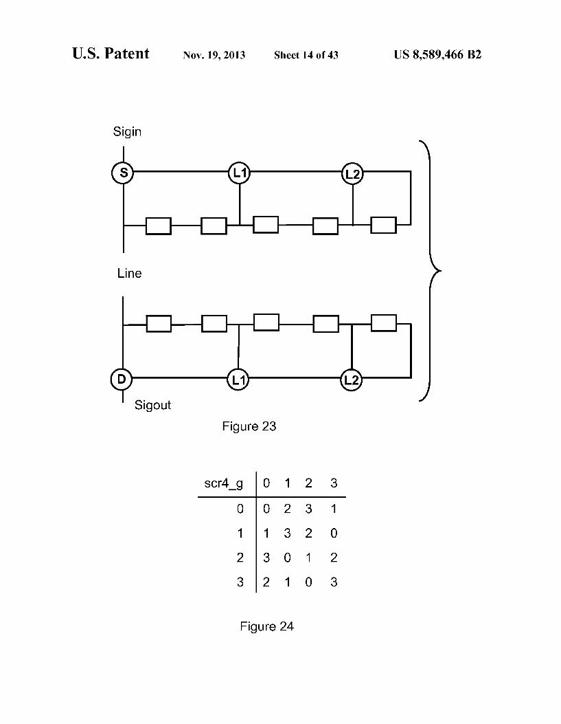
U.S. Patent Nov. 19, 2013 Sheet 14 of 43 US 8,589.466 B2
Sigin
Line
Figure 24
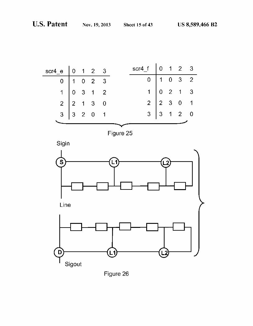
U.S. Patent Nov. 19, 2013 Sheet 15 of 43 US 8,589.466 B2
Figure 26
U.S. Patent Nov. 19, 2013 Sheet 16 of 43 US 8,589.466 B2
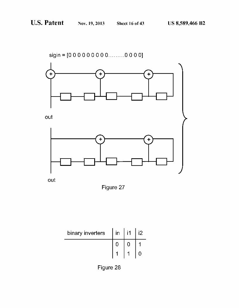
sigin = 00 00 00 000......... 0 0 O Ol
Out
Out Figure 27
binary inverters in 1 i2
Figure 28
U.S. Patent Nov. 19, 2013 Sheet 17 of 43 US 8,589.466 B2
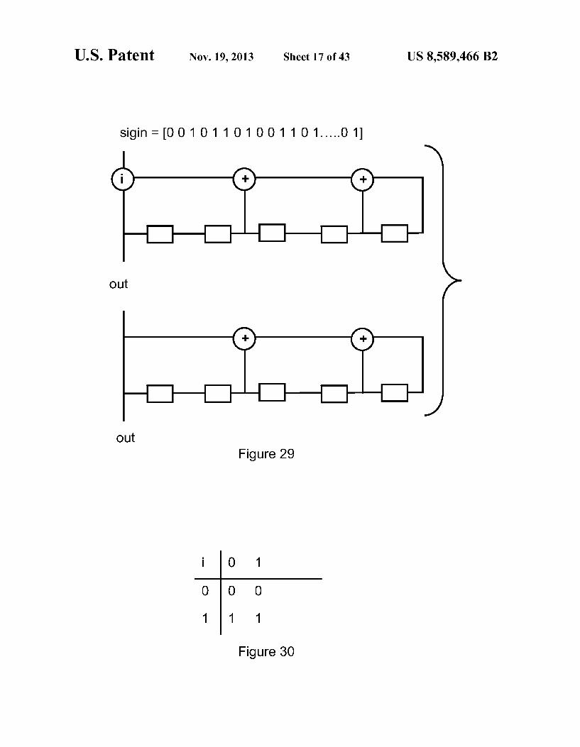
sigin = 0 0 1 0 1 1 0 1 0 0 1 1 0 1.01
Out
Out Figure 29
Figure 30
U.S. Patent Nov. 19, 2013 Sheet 18 of 43 US 8,589.466 B2
Figure 31
input input
O O O O
1 x 1 = 1 1 x 2 = 2
2 2 2 1
Figure 32
U.S. Patent Nov. 19, 2013 Sheet 19 of 43 US 8,589.466 B2
input input O O O O
1 1 1 2
2 X 1 = 2 2 X 2 = 4
3 3 3 1
4. 4. 4. 3
input input O O O O
1 3 1 4
2 X 3 = 1 2 x 4 = 3
3 4. 3 2
4 2 4 1
Figure 33
In 1 (2) In 1mod Out Add MOd-3
In 2
Figure 34
U.S. Patent Nov. 19, 2013 Sheet 20 of 43 US 8,589.466 B2
Figure 35
equiv1
In 1 (2) Out
Add Mod-3
In 2
Figure 36
U.S. Patent Nov. 19, 2013 Sheet 21 of 43 US 8,589.466 B2
equiv2
Out
Figure 38
U.S. Patent Nov. 19, 2013 Sheet 22 of 43 US 8,589.466 B2
Figure 39
Figure 40
U.S. Patent Nov. 19, 2013 Sheet 23 of 43 US 8,589.466 B2
60
40
O 2O 40 60 8O 1OO 12O 140 160
Figure 41
U.S. Patent Nov. 19, 2013 Sheet 24 of 43 US 8,589.466 B2
60
40
20
O 20 40 60 80 1OO 120 140 160
Figure 42
U.S. Patent Nov. 19, 2013 Sheet 25 of 43 US 8,589.466 B2
-10; 2O 40 60 8O 100 120 140 160
Figure 43
U.S. Patent Nov. 19, 2013 Sheet 26 of 43 US 8,589.466 B2
O 20 40 60 8O 100 120 140 160
Figure 44
U.S. Patent Nov. 19, 2013 Sheet 27 of 43 US 8,589.466 B2
6O
50
40
30
20
1O
O 20 40 60 8O 100 120 140 160
Figure 45
U.S. Patent Nov. 19, 2013 Sheet 28 of 43 US 8,589.466 B2
Figure 46
U.S. Patent Nov. 19, 2013 Sheet 29 of 43 US 8,589.466 B2
60
40
20
-20
-40
Figure 47
U.S. Patent Nov. 19, 2013 Sheet 30 of 43 US 8,589.466 B2
60
40
O 2O 40 60 80 1OO 120 140 160
Figure 48
U.S. Patent Nov. 19, 2013 Sheet 31 of 43 US 8,589.466 B2
control input is 'O'
Conducting state
Figure 49
control input is '1' or "2" but not 'O'
Non-Conducting state
Figure 50
U.S. Patent Nov. 19, 2013 Sheet 32 of 43 US 8,589.466 B2
l4 4
O 1 1 1 2 1 inv 2 = 2 inv 2 = O 2 O O O 1
Figure 51
5 15
O 2 2 2 1 1 inv O F O inv O = O 2 1 1 1 2
Figure 52
ternary 0 1 2
O 2 2 O
1 O O 1
2 1 O 2
Figure 53
U.S. Patent Nov. 19, 2013 Sheet 33 of 43 US 8,589.466 B2
= gate is conducting for control input is 'O'
2
O = universal ternary inverter i5:0 1
Figure 54
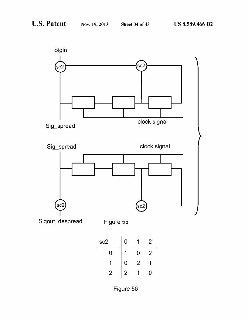
U.S. Patent Nov. 19, 2013 Sheet 34 of 43 US 8,589.466 B2
Clock Sional Sig Spread C
Sig Spread clock signal
Sigout despread Figure 55
Figure 56
U.S. Patent Nov. 19, 2013 Sheet 35 of 43 US 8,589.466 B2
Sigin = OOOOOOOOOOOOOOOOOOOOOOOOOO)
Sig spread 0 = 1 2002 02 221 1 0 2 120 02 0222 1102)
Sigin = 11111111111111111111111111
Sig spread 1 = 0 1 1 0 1 0 00 22 1 02 0 1 1 0 1 0 00 22 102)
Sigin = 22222222222222222222222222)
Sig spread 2 = 202 00 0 1 12 0 1 0 220 200 0 1 120 102)
Figure 57
20
15
10
5
O O 20 3O 40 50 O 1 60
Figure 58
U.S. Patent Nov. 19, 2013 Sheet 36 of 43 US 8,589.466 B2
15
10
Figure 59
20
15
1O
O 10 2O 30 40 50 60
Figure 60
U.S. Patent Nov. 19, 2013 Sheet 37 of 43 US 8,589.466 B2
20
15
10
Figure 61
U.S. Patent Nov. 19, 2013 Sheet 38 of 43 US 8,589.466 B2
Spreader
clock signal
Sig Spread
Despreader
Sig Spread clock signal
Figure 62
U.S. Patent Nov. 19, 2013 Sheet 39 of 43 US 8,589.466 B2
Figure 65
U.S. Patent Nov. 19, 2013 Sheet 40 of 43 US 8,589.466 B2
30
20
1O
O 20 40 60 80 1OO 120 140 160
Figure 66
US 8,589.466 B2 Sheet 41 of 43 Nov. 19, 2013 U.S. Patent
/9 ?un61–
al
and JB
amid.
U.S. Patent Nov. 19, 2013 Sheet 42 of 43 US 8,589.466 B2
O 2 1 O 3
1 1 O 3 2
2 O 3 2 1
3 3 2 1 O
Figure 68
US 8,589.466 B2 Sheet 43 of 43 Nov. 19, 2013 U.S. Patent
?nd?nO
69 ?un61–
- - -
and J3 -
| Ieußis pepeelds en?ea-º,
- x - x
apid. It
US 8,589,466 B2 1.
TERNARY AND MULTI-VALUE DIGITAL SIGNAL SCRAMBLERS, DECRAMBLERS
AND SEQUENCE GENERATORS
STATEMENT OF RELATED CASES
This application is a continuation of U.S. patent applica tion Ser. No. 1 1/618,986 filed on Jan. 2, 2007 which is a continuation-in-part of U.S. patent application Ser. No. 10/935,960 filed on Sep. 8, 2004, now U.S. Pat. No. 7,643, 632, issued Jan. 5, 2010, which claims the benefit of U.S. provisional patent application Ser. No. 60/547,683 filed on Feb. 25, 2004, of which all of the above are incorporated herein by reference in their entirety.
BACKGROUND OF THE INVENTION
This invention relates to the scrambling of multi-value digital (non-binary) signals and the generation of multi-value (non-binary) digital signals consisting of sequences of multi value (non-binary) digital elements such as n-value pseudo noise sequences. Multi-value signals, also referred to as X-value signals, can assume one of X states, wherein X is greater than or equal to three.
Its potential application is in telecommunication systems, control systems and other applications. Specific examples of utility where the invention can be used include spread-spec trum technologies, signal Scrambling, CDMA, line-coding and scrambling application in video and other signal distri bution.
Digital Scramblers are used to change the appearance of a digital signal in such away that during transmission the signal is different from the original signal. The original signal can be recovered from the scrambled signal at the receiving end by a descrambler. Most commonly in today's telecommunica tions, the scramblers relate to binary signals.
Scrambling of a binary signal can be achieved by combin ing the binary signal to be scrambled with a second known binary signal through a digital circuit that has the character istics of a reversible function. The inventor has recognized that the reversible function has the property that its two inputs generate an output. When applying this output as the input to another, but similar, circuit with as the other input a signal similar to the known input of the first digital circuit, the output of the second circuit is identical to the to be scrambled data signal input of the first circuit. This other circuit is a descram bler.
There are two known binary functions that can perform this reversible function: the Exclusive Or (XOR) and the Equal function. The XOR function is also known as the modulo-2 adding function.
Telecommunication markets such as wireless communica tions and internet communications demonstrate an ongoing increase in demand for higher information transmission rates. This demand in increased information transmission rates in wireless communications is addressed by increasing band width of communication channels, by compression of the information and by moving into much higher radio spectra (such as Ultra Wide Band in the 5 GHZ, area). Eventually, new technology has to be applied to obtain better performance from existing bandwidth, starting with highly congested spectrum areas. Current transmission technology predomi nantly uses digital binary signals. One possible technology to provide better bandwidth usage is the application of multi value digital signals. Scrambling, descrambling and signal sequence generation is an important element of signal pro cessing technology, especially in wireless communications.
10
15
25
30
35
40
45
50
55
60
65
2 However, currently very little technology exists in prior art that can perform multi-value digital Scrambling, descram bling and sequence generation. Most of prior art in scram bling, descrambling and sequence generation only performs binary functions, as previously discussed.
Consequently, new and improved methods and apparatus to perform scrambling, descrambling and sequence genera tion on non-binary, multi-value digital signals are required. The existence of multi-value reversible logic functions has
been previously mentioned. However, no mention has been found of multi-value reversible logic in scrambling/descram bling applications, nor in the generation of multi-value signal Sequences.
SUMMARY OF THE INVENTION
In view of the more limited possibilities of the prior art in binary and multi-value Scrambling (or reversible) logic func tions, the current invention offers an easier design as well as a greater variety in multi-value scramblers and in LFSR based sequence generators. It also provides improved performance. The general purpose of the present invention, which will be
described Subsequently in greater detail, is to provide new scrambler/descrambler systems and LFSR based generators of multi-value signal sequences. It also provides a new elec tronic circuit and gates to process multi-value signals, and provides sequence generators with reduced component and COunt.
Before explaining at least one embodiment of the invention in detail it is to be understood that the invention is not limited in its application to the details of construction and to the arrangements of the components set forth in the following description or illustrated in the drawings. The invention is capable of other embodiments and of being practiced and carried out in various ways. Also, it is to be understood that the phraseology and terminology employed herein are for the purpose of the description and should not be regarded as limiting.
Multi-value and n-value in the context of this application mean a number n, with n being a positive integer greater than tWO.
A primary object of the present invention is to provide new multi-value scrambler/descrambler systems that will over come the shortcomings of the prior art devices. An object of the present invention is to provide a maximum
set of multi-value digital, single function, Scrambling/de scrambling devices.
Another object is to provide new LFSR based multi-value digital scramblers and self synchronizing LFSR based descrambler devices.
Another object is to provide a method for applying multi value logic scrambling/descrambling functions in a LFSR architecture to generate multi-value digital signal sequences.
Another object of the invention is to providen-Value LFSR based scramblers/descramblers as n-value signal spreaders/ despreaders with no synchronization requirements. AS is known, these are easier to realize, but provide less security.
Another object of the invention is to providen-Value LFSR based scramblers/descramblers as n-value signal spreaders/ despreaders with synchronization requirements. As is known, these are harder to realized, but provide higher security.
Another object is to provide multi-value digital inverters that will change the value of a multi-value signal without upsetting the distinguishing characteristics of the individual elements of a digital signal.
US 8,589,466 B2 3
Another object is to provide composite systems compris ing two or more individual systems that are connected through components that execute multi-value logic digital scrambling functions.
Another object is to provide a method called “design by inverters’ that allows creating any multi-value truth table for scrambling and descrambling functions from a set of indi vidual multi-value digital inverters.
Another object of the invention is to provide a method to translate prior art modulo-n adder functions combined with n-value multipliers at the inputs into n-value scrambling func tions of this invention.
Another object of the invention is to apply multi-value logic reversible inverters to received signals in order to bring desired auto-correlation and cross-correlation levels of the signals to Zero.
Another object of the invention is to provide a method for creating multi-value logic devices of which the scrambling functions are a Subset, by applying components which only consist of the following types: a gate and a universal multi value inverter.
Prior art in scrambling/descrambling and signal sequence generation mainly applies binary technology. Even in cases where multi-value digital signals are generated the Scram bling, descrambling and sequence generation is based on modulo-2 theory and embodiment. In some cases modulo-n addition theory and embodiment is proposed. However modulo-naddition is a non-self reversing technology. AS Such modulo-n addition requires a reversing function to create a n-value scrambler/descrambler set. Also modulo-n addition solution in creating LFSR based scramblers, descramblers and sequence generators require multipliers to achieve statis tically optimal performance.
Consequently the present invention offers a much broader, more diverse and easier method to create multi-value Scram blers, descramblers and signal sequence generators. Com bined with prior art in realizing multi-value logic electronic embodiments this invention can prevent the need for “switch ing back to binary logic' in multi-value logic signal process ing applications. Prior art Such as realizing adequate 4B3T transmission signals demonstrates the overhead from binary logic to manage ternary (3-value) signal generation and recovery with binary logic circuitry. One aspect of the present invention provides multi-value
functions, including ternary and higher multi-value func tions, that are useful in many applications, including those requiring scrambling, descrambling, spreading, dispreading and sequence generation.
In accordance with one aspect of the present invention, a method of Scrambling a ternary signal with a scrambler is provided. The ternary signal is able to assume one of three states and the scrambler has a first Scrambling ternary logic device that implements a ternary logic function, Sc., and a scrambling logic circuit. The method involves inputting the ternary signal and an output from the Scrambling logic circuit to the first scrambling ternary logic device and inputting an output from the first scrambling ternary logic device to the scrambling logic circuit. The ternary logic function, sc, can be specified by a scrambling ternary truth table having three columns, and each of the columns being defined by a ternary inverter. When the ternary signal is input, the output from the first scrambling ternary logic device is a scrambled version of the ternary signal.
In accordance with another aspect of the present invention, each column is defined by one of the following ternary invert ers i to i:
10
15
25
30
35
40
45
50
55
60
65
11 12 13 i4 15 16
O O O 1 1 2 2 1 1 2 O 2 O 1 2 2 1 2 O 1 O
It is noted, however, that every column cannot be defined by the identity inverter i. In that case, there would be no scrambling performed.
In accordance with a further aspect of the present inven tion, at least one ternary inverter can be used to define a scrambling ternary truth table with the exception of the iden tity inverter, as described in the previous paragraph. Also, more than one ternary inverter can be used to define a scram bling ternary truth table.
In one embodiment of the present invention, the scram bling logic circuit includes a scrambling n-length shift regis ter having n elements and a first and a second scrambling ternary logic device, the Scrambling n-length shift register having outputs from two of then elements that are provided to two inputs of the second scrambling ternary logic device, and wherein the output from the first scrambling ternary logic device is provided to an input of then-length shift register and an output of the second scrambling ternary logic device is provided to an input of the first scrambling ternary logic device. One of the inputs to the second scrambling ternary logic device is usually from the last element in the n-length shift register. Further, additional ternary logic devices and taps from additional or different elements in the shift register can be used. The ternary logic devices implement a ternary logic function that is defined by ternary inventors.
For example, the Scrambling logic circuit could include a scrambling n-length shift register having n elements and at least one second scrambling X-value logic device (where X is greater than or equal to three). There are, at most, n-1 second scrambling X-value logic devices. The n-1 X-Value second logic devices can be functionally equivalent or can be differ ent, but each are specified by a x-value scrambling truth table having X columns, each of the X columns being defined by one of X reversible X-value inverters and wherein not all of the columns are defined by the identity inverter. Each of the n-1 X-value second logic devices has two inputs and one output. One of the inputs of each of the n-1 x-value second logic devices is uniquely connected with an output of an element of the n-length shift register. If there are two or more second logic devices in the scrambling logic circuit then the second logic devices have as their second input the output of the next second logic device, with exception of the last second logic device which has the output of then-length shift register as is second input. The output of the first (and possibly only) second logic device is the output of the Scrambling logic circuit.
In accordance with a further aspect of the present inven tion, the scrambled version of the ternary signal is descrambled with a descrambling device. The descrambling device is related and similar to the scrambler. The descram bling device has a first descrambling ternary logic device and a descrambling logic circuit. The first descrambling ternary logic device implements a ternary logic function, dc. The method of descrambling includes inputting the scrambled version of the ternary signal to the first descrambling ternary logic device and to the descrambling logic circuit, inputting an output from the descrambling logic circuit to the first descrambling ternary logic device, and outputting a descrambled ternary signal on an output of the first descram
US 8,589,466 B2 5
bling ternary logic device. The ternary logic function, dc, can be specified by a descrambling ternary truth table having three columns, and each of the columns is defined by one of the ternary inverters i to it.
In accordance with another aspect of the present invention, 5 a column in the descrambling ternary truth table is defined by: (1) the same inverter that defines the corresponding column in the Scrambling ternary truth table if the inverter is i, i, is or i; (2) the inverteris if the corresponding column in the scram bling ternary truth table is defined by the inverteria; and (3) the inverter i if the corresponding column in the scrambling ternary truth table is defined by the inverter is.
In accordance with another aspect of the present invention, a column in the descrambling ternary truth table is defined by:
10
(1) the same inverter that defines the corresponding column in 15 the scrambling ternary truth table if the inverter is self revers ing and (2) a different inverter if the corresponding column in the scrambling ternary truth table is defined by a reversible inverter that is not self-reversing. This also applies to the multi-value case where a signal represents one of four or more values.
In accordance with one embodiment of the present inven tion, the Scrambling logic circuit includes a scrambling n-length shift register having n elements and a second scram bling ternary logic device, the scrambling n-length shift reg ister having outputs from two of the n elements that are provided to two inputs of the second scrambling ternary logic
device, and wherein the output from the first scrambling ternary logic device is provided to an input of the n-length shift register and an output of the second scrambling ternary logic device is provided to an input of the first scrambling ternary logic device. The corresponding descrambling logic circuit includes a descrambling n-length shift register having in elements and a second descrambling ternary logic device, the scrambling n-length shift register having outputs from two of the n elements that are provided to two inputs of the second descrambling ternary logic device, and wherein the output from the second descrambling ternary logic device is provided to an input of the first descrambling ternary logic device and the scrambled version of the ternary signal is input to the descrambling n-length shift register. The descrambling unit is similar and related to the Scrambling unit, having the same length of shift register, output taps at the same positions and applying identical ternary functions.
In accordance with another aspect of the present invention, apparatus for Scrambling a ternary signal that can assume one of three states is provided. The apparatus includes a first scrambling ternary logic device that implements a ternary logic function, sc, the first Scrambling ternary logic device having a first and second input and an output. It also includes a scrambling logic circuit having an input and an output. The ternary signal is input to the first input of the first scrambling ternary logic device, the output of the scrambling logic circuit is input to the second input of the first Scrambling ternary logic device and the output of the first scrambling ternary logic device is provided to the input of the scrambling logic circuit. The ternary logic function, sc, can be specified by a
25
40
45
50
55
60
65
6 scrambling ternary truth table having three columns, each of the columns being defined by a ternary inverter. A scrambled ternary signal is provided on the output of the first scrambling ternary logic device.
Apparatus for descrambling ternary signals is also pro vided in accordance with the present invention. The apparatus for Scrambling and descrambling ternary signals corre sponds, for the most part, to the previously described method for Scrambling and descrambling ternary signals. The present invention also provides method and apparatus
for Scrambling and descrambling multi-value signals that can assume one of X states, wherein X is greater than or equal to 4. The scrambler has a first Scrambling multi-value logic device that implements a multi-value logic function, fisc, and a scrambling logic circuit. The method involves inputting the multi-value signal and an output from the scrambling logic circuit to the first Scrambling multi-value logic device and inputting an output from the first scrambling multi-value logic device to an input to the scrambling logic circuit. The multi-value logic function, fisc, can be specified by a multi value Scrambling truth table having X columns, each of the columns being defined by a multi-value inverter. The output from the first Scrambling multi-value logic device is a scrambled version of the multi-value signal.
In the case where X equals 4, each column is defined by one of the following multi-value inverters i to i:
In accordance with one aspect of the present invention, at least one different multi-value inverter defines a multi-value truth table, as long as every column is not defined by the identity inverter for scrambling applications. Alternatively, a greater number of different multi-value inverters can define the multi-value truth table.
Further, the invention is applicable where x is greater than four. There are x reversible inverters in any x-value logic system. The scrambling logic circuit for processing the multi-value
signal is similar to the scrambling logic circuit for processing the ternary logic signal. It includes a scramblingn-length shift register having n elements and one or more second scram bling multi-value logic device. The scrambling n-length shift register has outputs from two of the n elements that are provided to two inputs of one of the second scrambling multi value logic device. The output from the first scrambling multi-value logic device is provided to an input of the n-length shift register and an output of the second scrambling multi-value logic device is provided to an input of the first scrambling multi-value logic device. As before, additional logic devices and additional taps can be used.
In accordance with another aspect of the present invention, the scrambled version of the multi-value signal is descrambled with a descrambling device having a first descrambling multi-value logic device and a descrambling logic circuit. The first descrambling multi-value logic device implementing a multi-value logic function, fac. The method involves inputting the scrambled version of the multi-value signal to the first descrambling multi-value logic device and
US 8,589,466 B2 7
to the descrambling logic circuit, inputting an output from the descrambling logic circuit to the first descrambling multi value logic device and outputting a descrambled multi-value signal on an output of the first descrambling multi-value logic device. The multi-value logic function, fac, can be specified by a descrambling multi-value truth table having X columns, and each of the columns is defined by one of the multi-value inverters i to it, if X is equal to 4. Again, the descrambling unit is related and similar to the scrambling unit, as previously described.
In accordance with another aspect of the present invention, a column in the descrambling multi-value truth table is defined by: (1) the same inverter that defines the correspond ing column in the scrambling multi-value truth table if the inverter is self reversing; and (2) a different inverter if the corresponding column in the scrambling multi-value truth table is defined by a reversible inverter that is not self-revers ing.
In accordance with another aspect of the present invention, a multi-value sequence generator is provided. The sequence generator includes a shift register having a plurality of n elements and one or more (but not more than n-1) multi-value logic devices, each having a first input, a second input and an output. The output from one (but generally not the last) of the plurality of elements is connected to the first input of the first multi-value logic device. If the first multi-value logic device is the only logic device, the output of the last of the plurality of elements is connected to the second input of the multi value logic device and the output from the first or only multi value logic device is connected to the input of the first of the plurality of elements. If there are two or more multi-value logic devices in the sequence generator, the second input of the first multi-value logic device is connected with the output of the next multi-value logic device. The next multi-value logic device has two inputs. The first input of the next multi value logic device is connected with a unique output of the plurality of elements of the shift register (but not with the last one). The second input of the next multi-value logic device is connected with the output of the following multi-value logic device, unless this next multi-value logic device is the final one. In that case its second input is connected with the output of the last element of the plurality of elements of the shift register.
In accordance with another aspect of the present invention an electronic circuit for implementing a ternary logic function is provided. The ternary logic function can be defined by a truth table that has a first column defined by a first ternary inverter, a second column defined by a second ternary inverter and a third column defined by a third ternary inverter. The electronic circuit processes the ternary logic signal and a second input signal, both signals being able to assume a first state, a second State and a third State, such that it implements the ternary logic function defined by the truth table.
The electronic device has a first input port for the ternary logic signal, a second input port for the second input signal and an output. The electronic device also has a first channel including a series connection of the first ternary inverter and first Switching means for connecting the first input to the output when the second input signal assumes a first of the three states. This first channel implements the first column of the truth table defining the ternary logic function. It also has a second channel including a series connection of the second ternary inverter and second Switching means for connecting the first input to the output when the second input signal assumes a second of the three states. This second channel implements the second column of the truth table defining the ternary logic function. It also has a third channel including a
5
10
15
25
30
35
40
45
50
55
60
65
8 series connection of the third ternary inverter and third Switching means for connecting the first input to the output when the second input assumes a third of the three states. The third channel implements the third column of the truth table defining the ternary logic function.
BRIEF DESCRIPTION OF THE DRAWINGS
Various other objects, features and attendant advantages of the present invention will become fully appreciated as the same becomes better understood when considered in con junction with the accompanying drawings, and wherein:
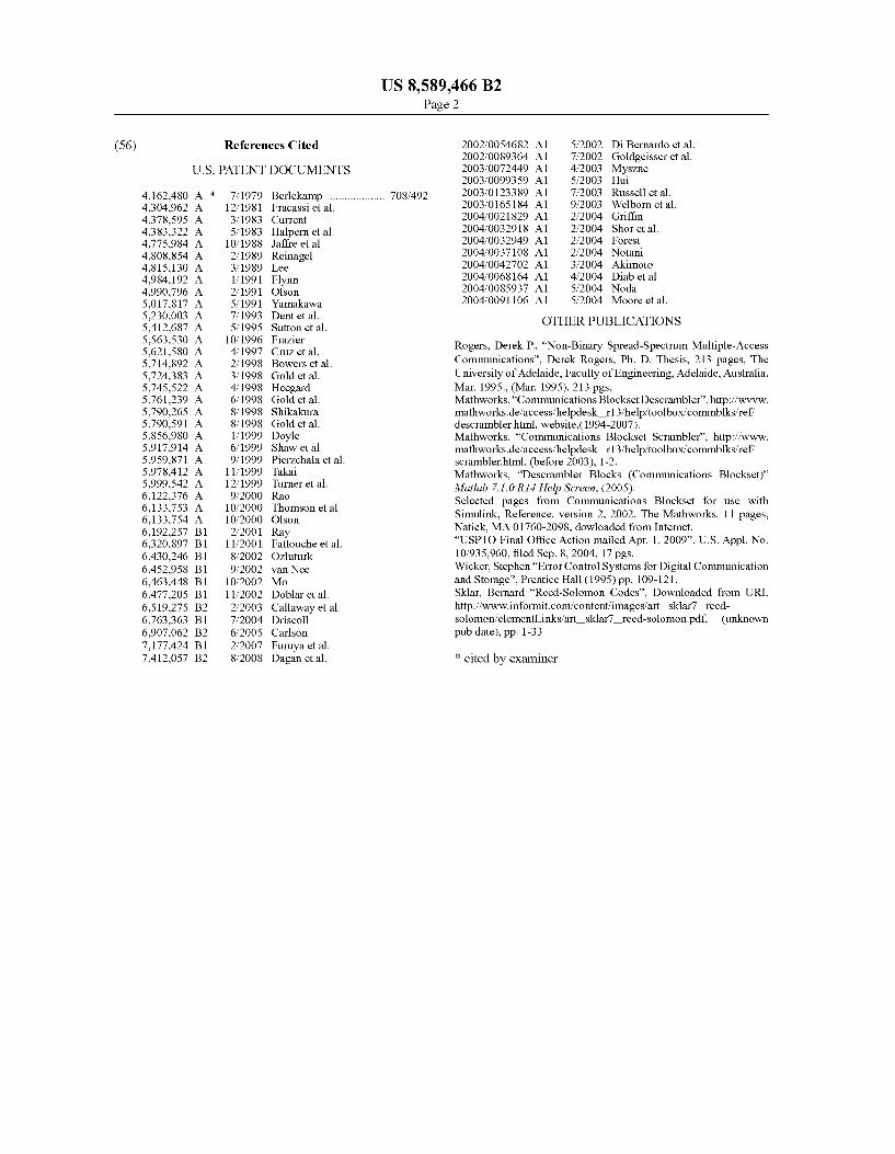
FIG. 1 is a diagram showing a five stage Linear Feedback Shift Register binary scrambler with feedback taps at the output of shift register stage 2, 4 and 5 and a matching binary 5-stage LFSR based descrambler;
FIG. 2 is a diagram showing a binary 5-stage Linear Feed back Shift Register (LFSR) based binary sequence generator;
FIG. 3 shows the truth table of a 2 input single output binary function that passes on the value of one input regard less of the value of the other input;
FIG. 4 shows a diagram of a binary 5-stage LFSR based scrambler applying the function described in FIG.3 to form a binary sequence generator;
FIG. 5 shows the canonical form of a 2 input single output logic device, in this case, depicting a binary XOR or modulo-2 addition device;
FIG. 6 shows the truth table belonging to the 2 input single output XOR device:
FIG. 7 shows a two input (a and b) single output (c) ternary logic device Scr2:
FIG. 8 shows the ternary logic truth table for device scr2 of FIG.7; FIG.9 shows the truth tables for three self reversing ternary
logic functions; FIG.10 shows the canonical truth table of the self reversing
n-value logic function, in accordance with one aspect of the present invention;
FIG. 11 shows a table of six ternary reversible inverters in accordance with one aspect of the present invention;
FIG. 12 shows a table of a symbolic representation of four (4) self reversing ternary inverters including the identity inverter and also shows a truth table of a self reversing scram bling function;
FIG.13 shows the truth tables belonging to a pair ofternary reversible functions that are each others reverse but are not self reversing:
FIG. 14 shows a diagram of two devices that embody the two ternary functions of FIG. 13 that demonstrate the scram bling and descrambling capabilities;
FIG. 15 shows a truth table of a weak ternary scrambling function;
FIG.16 shows a table of 24 reversible 4-value logic invert ers including the identity function;
FIG. 17 shows 4 self reversing 4-value logic truth tables that are not equal to the 4-value logic canonical self reversing functions;
FIG. 18 shows a diagram of a prior art binary Linear Feed back Shift Register based binary scrambler and its matching descrambler;
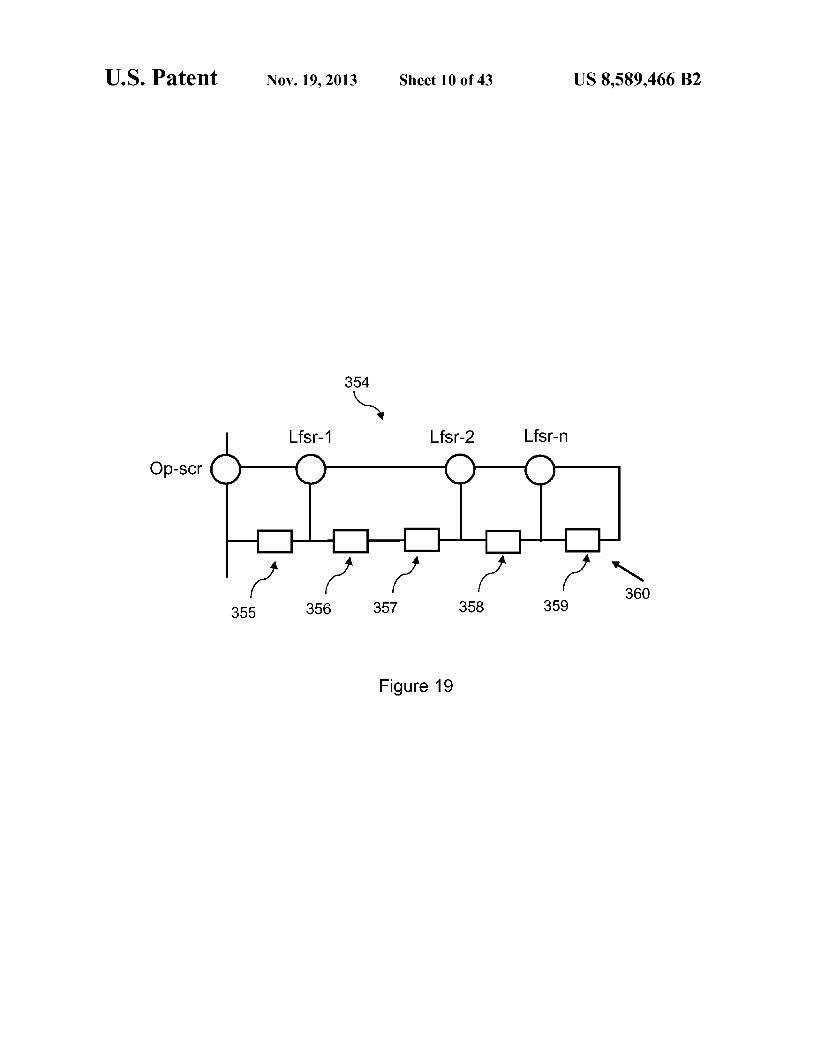
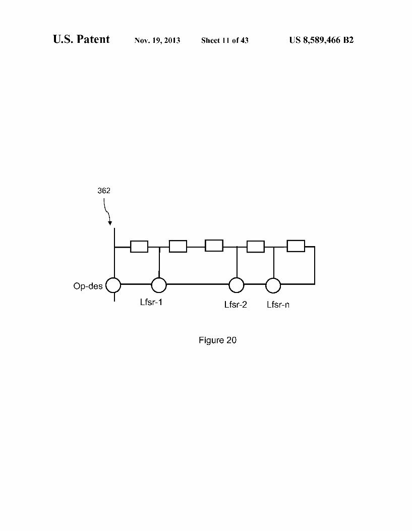
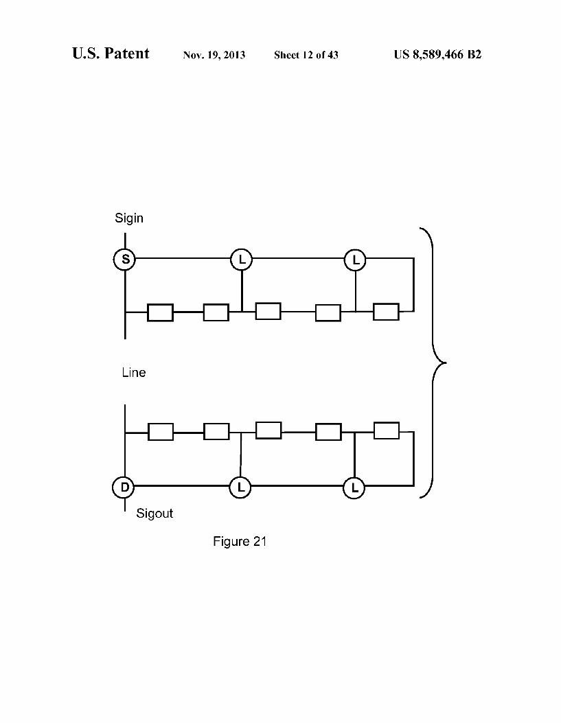
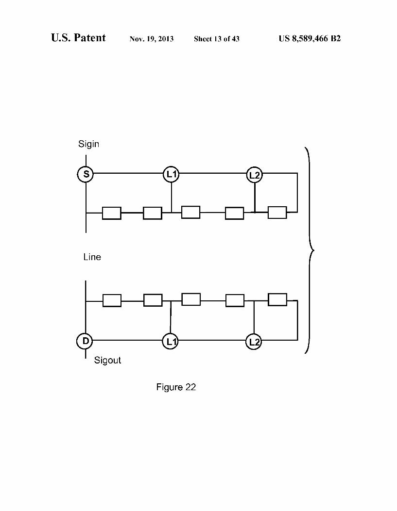
FIG. 19 shows a multi-value LFSR based scrambler; FIG. 20 shows a multi-value LFSR based descrambler; FIG. 21 shows a 4-value 5-stage LFSR based scrambler
comprising only one type of self-reversing commutative function and its matching descrambler;
US 8,589,466 B2 9
FIG. 22 shows a 4-value 5-stage LFSR based scrambler comprising 3 different types of self-reversing commutative function and its matching descrambler;
FIG. 23 shows a 4-value 5-stage LFSR based scrambler comprising 2 different types of self-reversing commutative function and one type of non-commutative self-reversing function and its matching descrambler;
FIG.24 shows the truth table of a 4-value self-reversing but non-commutative function;
FIG. 25 shows a reversible commutative 4-value function and its reverse, a non-commutative reversible function;
FIG. 26 shows a 4-value 5-stage LFSR based scrambler comprising 4 different types of reversible functions and its matching descrambler, the different functions having two types of 4-value self reversing functions, one commutative reversible function and its reverse, a 4-value non-commuta tive reversible function;
FIG. 27 shows a binary LFSR based scrambler with con stant input and an equivalent circuit;
FIG. 28 shows two binary revertible inverters; FIG. 29 shows a binary LFSR based scrambler with a
non-constant input into a connecting identity function and an equivalent circuit;
FIG. 30 shows the truth table of the binary identity: FIG. 31 shows a generic 3-stage 2-tap n-value modulo-n
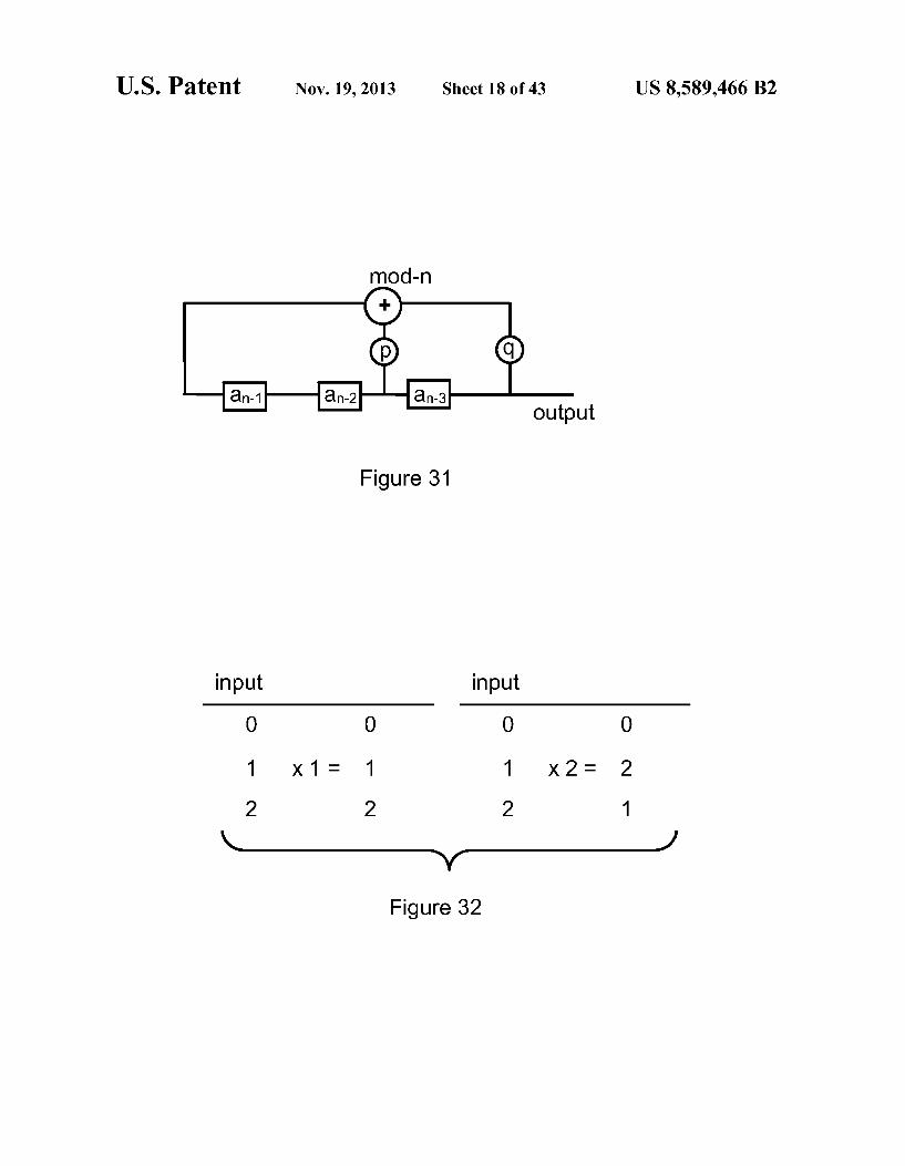
n-value sequence generator for which the inputs to the modulo-n adder are multiplied with factors p and q (modulo n);
FIG. 32 shows a table with the possible inputs to a ternary device multiplied by the possible values of p and q being 1 and 2 modulo-3 (zero is considered a trivial case);
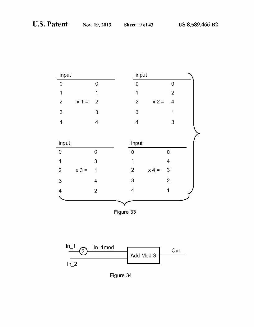
FIG.33 shows a table with the possible inputs to a 5-value device multiplied by the possible values of p and q being 1, 2, 3 and 4 modulo-5 (zero is considered a trivial case);
FIG. 34 shows a diagram of a 2 input single outputternary device with one of its inputs multiplied with a factor 2:
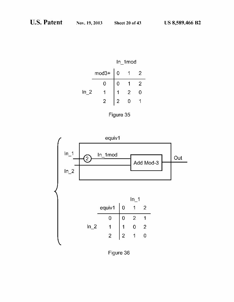
FIG. 35 shows the truth table of a modulo-3 adder; FIG.36 shows an equivalent depiction of the ternary device
of FIG. 34 and its corresponding truth table; FIG. 37 shows a diagram of a modulo-3 adder with the
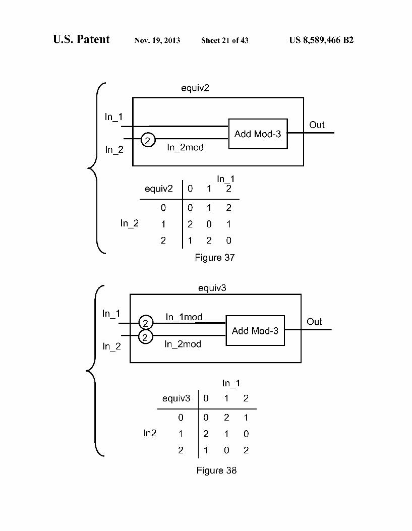
bottom input multiplied by 2 as well as the truth table for this circuit;
FIG. 38 shows a diagram of a modulo-3 adder with both inputs multiplied by 2 as well as the truth table for this circuit;
FIG. 39 shows a table of transformation for an n-value reversible inverter;
FIG. 40 shows a diagram of a one ternary function LFSR based sequence generator,
FIG. 41 shows the truth table ofternary reversible function ter1 applied in the lay-out of the ternary sequence generator as shown in FIG. 40, as well as a graph showing the auto correlation for the generated sequences;
FIG. 42 shows the truth table ofternary reversible function ter2 applied in the lay-out of the ternary sequence generator as shown in FIG. 40, as well as a graph showing the auto correlation for the generated sequences;
FIG. 43 shows the truth table ofternary reversible function ter5 applied in the lay-out of the ternary sequence generator as shown in FIG. 40, as well as a graph showing the auto correlation for the generated sequences;
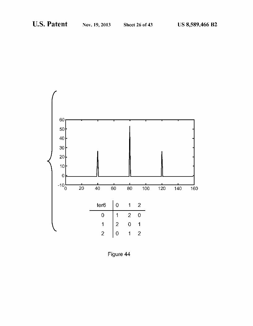
FIG. 44 shows the truth table ofternary reversible function ter6 applied in the lay-out of the ternary sequence generator as shown in FIG. 40, as well as a graph showing the auto correlation for the generated sequences;
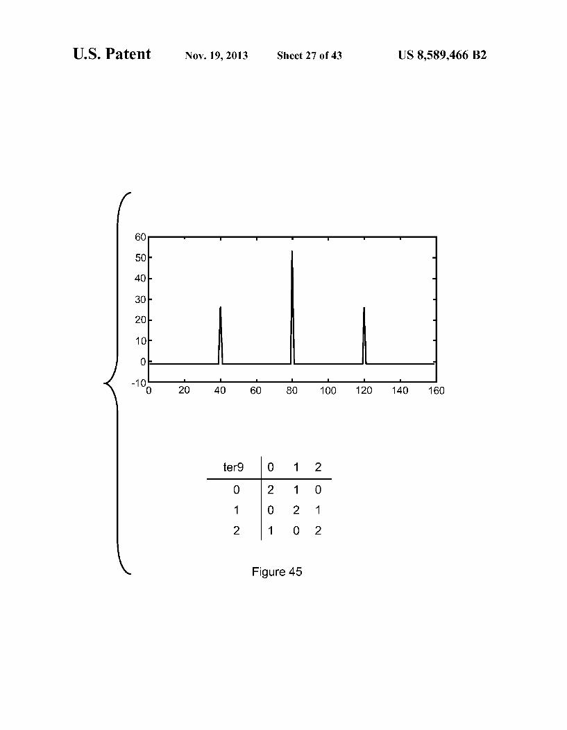
FIG. 45 shows the truth table ofternary reversible function ter9 applied in the lay-out of the ternary sequence generator
10
15
25
30
35
40
45
50
55
60
65
10 as shown in FIG. 40, as well as a graph showing the auto correlation for the generated sequences;
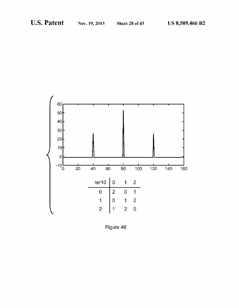
FIG. 46 shows the truth table ofternary reversible function ter10 applied in the lay-out of the ternary sequence genera tor as shown in FIG. 40, as well as a graph showing the auto-correlation for the generated sequences;
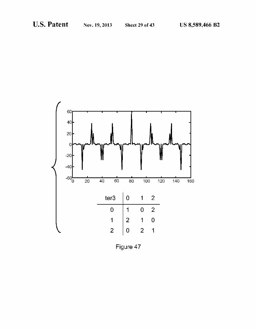
FIG. 47 shows the truth table ofternary reversible function ter3 applied in the lay-out of the ternary sequence generator as shown in FIG. 40, as well as a graph showing the auto correlation for the generated sequences;
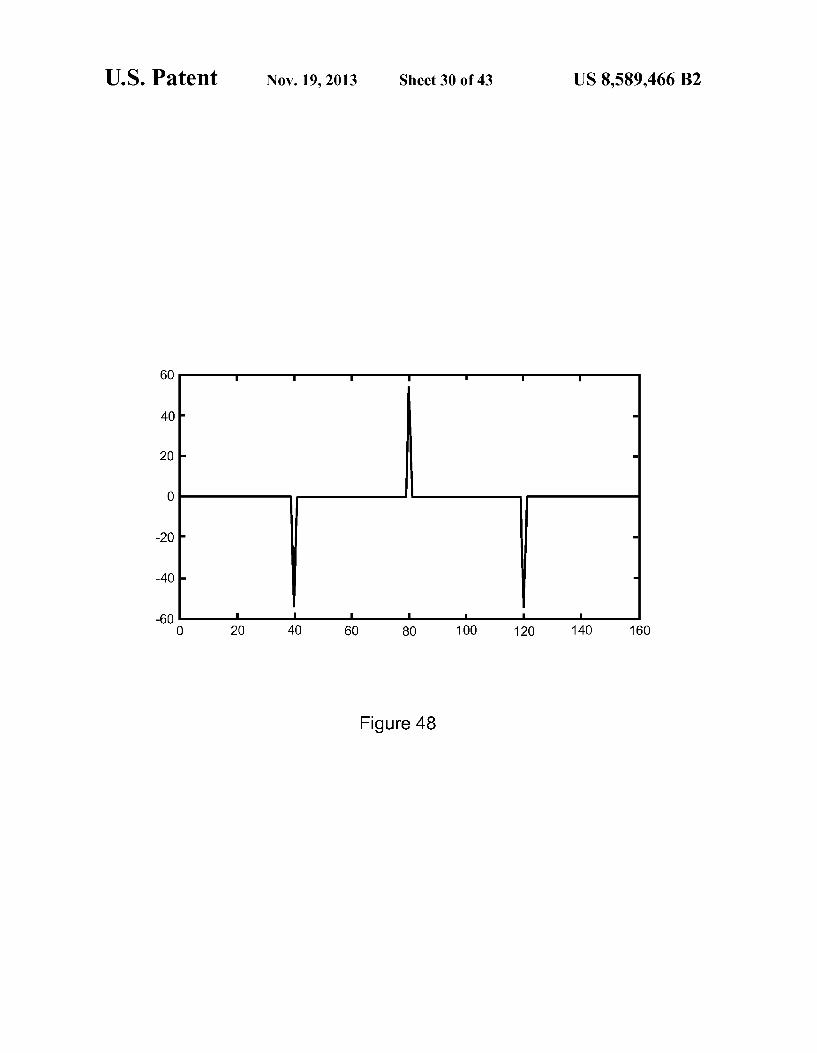
FIG. 48 shows agraph of the auto-correlation of a sequence generated by an LFSR based ternary sequence generator with the lay-out of FIG. 40 applying the ternary function ter10 and applying ternary inverter i3 as shown in the table of reversible ternary inverters in FIG. 11;
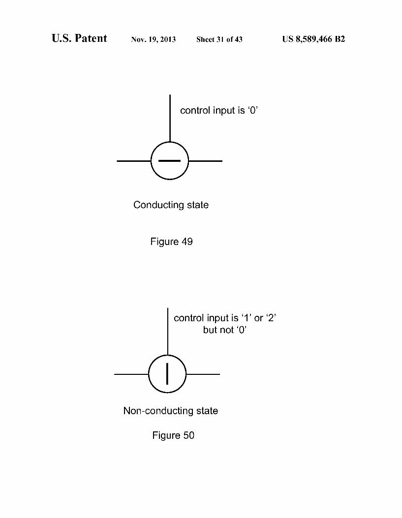
FIG. 49 shows a diagram of a conducting gate with the control input equal to 0:
FIG.50 shows a diagram of a non-conducting gate with the control input not equal to 0:
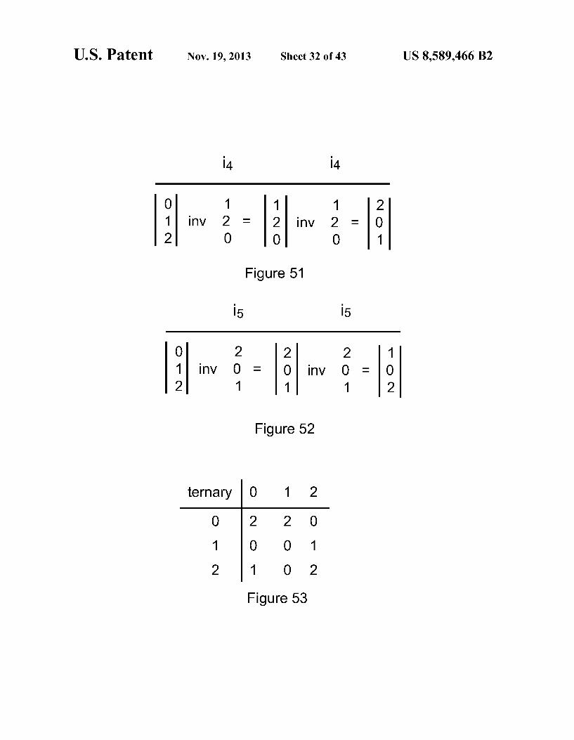
FIG. 51 shows a table applying ternary inverter i4 once and twice;
FIG. 52 shows a table applying ternary inverter i5 once and twice;
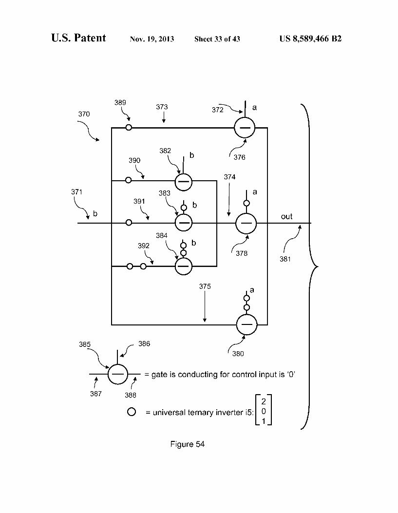
FIG. 53 is the truth table of a ternary function that will be realized in diagram with the gate/universal inverter method;
FIG. 54 shows a diagram of a ternary device realizing the truth table of FIG. 53 with the gate/universal ternary gate method; FIG.55 shows a diagram of a ternary LFSR based signal
spreader with its matching self-synchronizing LFSR based despreader wherein the applied scrambling function is the ternary function sc2;
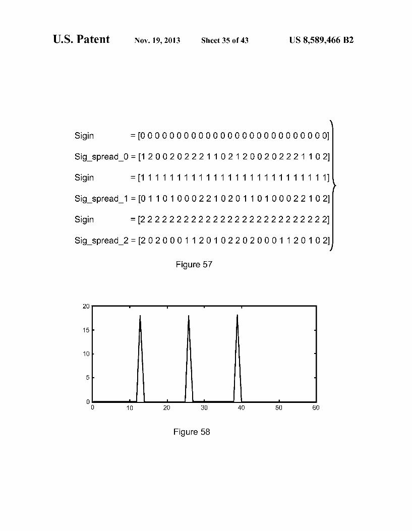
FIG. 56 shows the truth table of ternary logic function sc2; FIG. 57 shows a table of incoming ternary data signals and
the resulting spread signals as generated by the system as shown in FIG. 56;
FIG. 58 shows the autocorrelation graph for the spread signal created by spreading ternary input signal 0 with the spreading system as shown in FIG. 56;
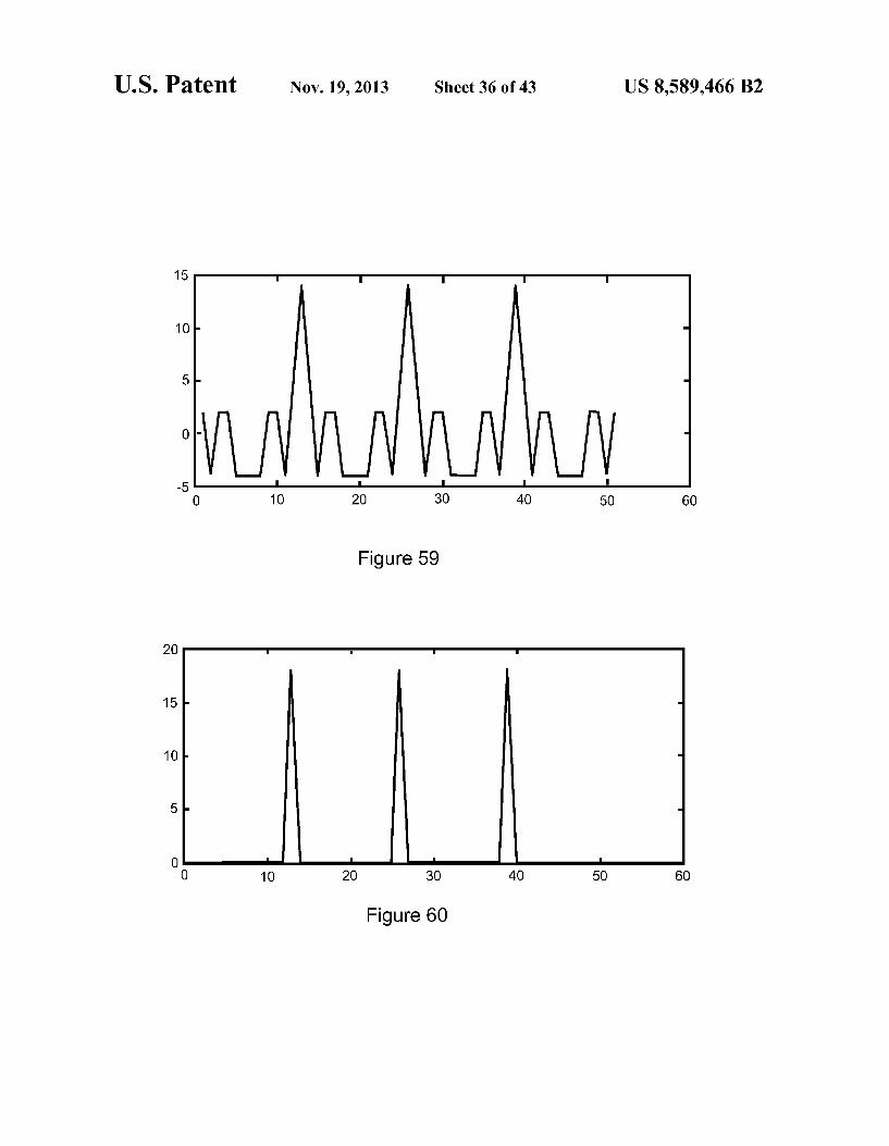
FIG. 59 shows the autocorrelation graph for the spread signal created by spreading ternary input signal 1 with the spreading system as shown in FIG. 56;
FIG. 60 shows the adjusted autocorrelation graph for the spread signal created by spreading ternary input signal 1 with the spreading system as shown in FIG. 56;
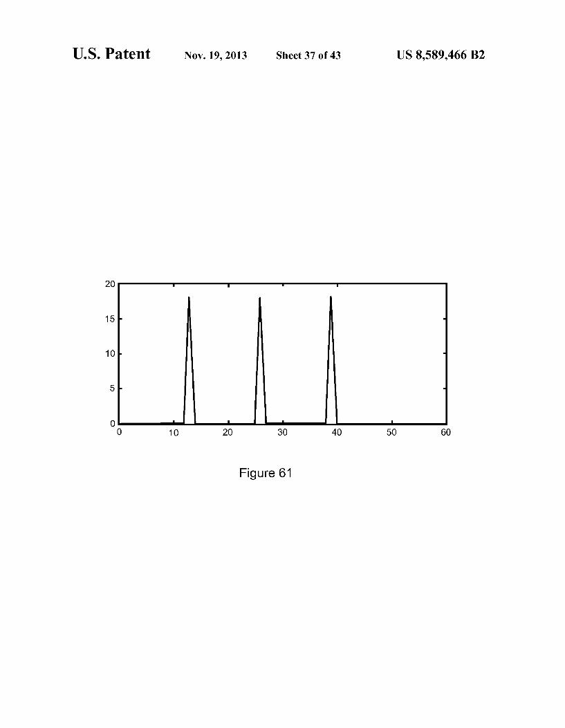
FIG. 61 shows the adjusted autocorrelation graph for the spread signal created by spreading ternary input signal 2 with the spreading system as shown in FIG. 56;
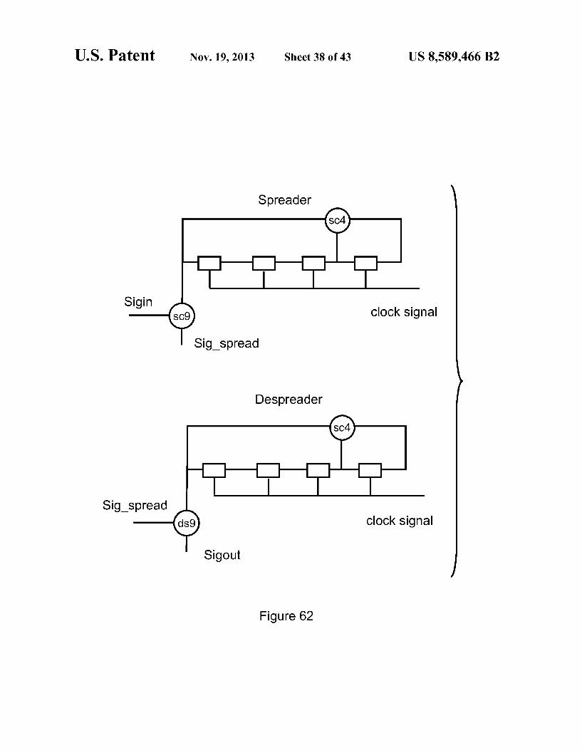
FIG. 62 shows a diagram of a ternary spreading/dispread ing System applying an independent sequence generator,
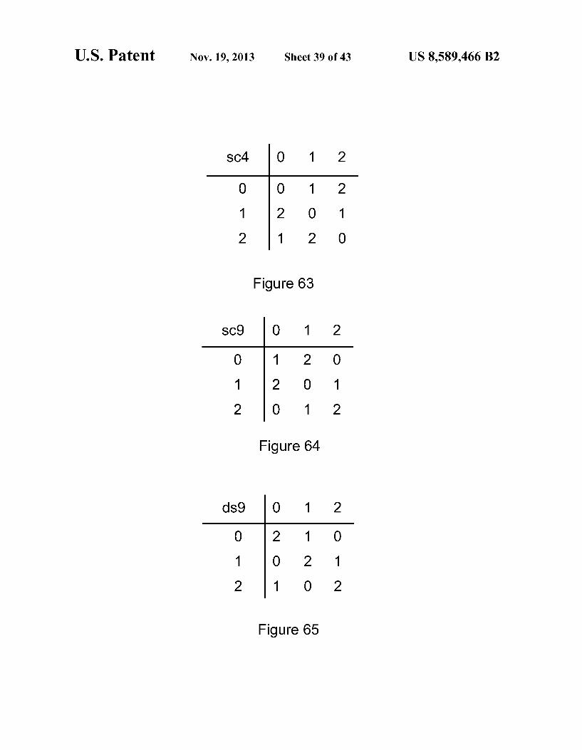
FIG. 63 shows the truth table of ternary logic function sc4; FIG. 64 shows the truth table of ternary logic function
“sc9; FIG. 65 shows the truth table for ternary logic function
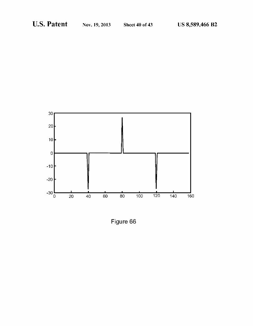
“ds9; FIG. 66 shows the cross correlation graph for the possible
ternary spread signals generated by the spreader as shown in the diagram of FIG. 62 and the ternary spreading sequence generated by the ternary LFSR based sequence generator wherein the ternary inverter i6 as shown in FIG. 11 is applied to the incoming spreaded signal before determining the cross correlation; and
FIGS. 67 to 69 illustrate further embodiments of the present invention.
US 8,589,466 B2 11
DETAILED DESCRIPTION OF THE INVENTION
The inventor has filed a provisional patent application that has been assigned Ser. No. 60/501,335 that relates to com mutative multi-value Scrambling/descrambling logic func tions. This provisional patent application contains a descrip tion of how these functions can be applied in signal scramblers and in LFSR based multi-value scramblers and descramblers. The disclosure, including the entire specifica tion and drawings, in provisional patent application Ser. No. 60/501,335, filed on Sep. 9, 2003, is hereby incorporated by reference in its entirety into this document. Also, the disclo Sure, including the entire specification and drawings, in non provisional patent application Ser. No. 10/912,954, filed on Aug. 6, 2004, that claims the benefit of provisional patent application Ser. No. 60/501,335 and is entitled TERNARY AND HIGHER MULTI-VALUE DIGITAL SCRAM BLERS/DESCRAMBLERS, is hereby incorporated by ref erence in its entirety into this document. Further, the entire disclosure, including the specification and drawings in the provisional patent application Ser. No. 60/547,683, filed Feb. 25, 2004, is hereby incorporated by reference into this docu ment.
While powerful in their own right, the application of the functions described in the aforementioned provisional patent application form a subset of a more elaborate collection of possible functions that are specified in this specification. The increased number of possible functions can provide a greater diversity and thus, among other benefits, a greater security.
Furthermore, in accordance with another aspect of the present invention, a new method referred to as “inverter based design' allows for designing, realizing and enabling commu tative as well non-commutative scrambling/descrambling functions. With the “inverter based' scrambling functions, multi-value pseudo-noise signal sequence generators can be created with a multi-value shift register, and these inverter based sequence generators do not require a multiplier. Thus, fewer components are required than previous designs.
Furthermore, in accordance with another aspect of the present invention, the “method of inverters' allows for creat ing electronic circuits executing multi-value Scramblers, descramblers and digital sequence generators by using a lim ited functional set of components including: a gate and a universal inverter and, if needed, A/D and D/A converters.
In accordance with one aspect of the present invention, the invention can contribute in obtaining better performance from existing bandwidth. For example, ternary and quater nary signals are used in line-coding to obtain a better usage from spectrum bandwidth. Signals are scrambled to avoid long series of constant values of a signal (such as long series of Zeros). Usually this involves scrambling of a binary signal followed by coding from binary to multi-value. In accordance with another aspect of the present invention, line-coding is made much less complex.
Spread-spectrum signals can be created by Scrambling a slow data signal with a much faster "chip” sequence. The signal can be de-spread, so that the original sequence is re created, by descrambling the received signal with a copy of the faster "chip” sequence. In accordance with one aspect of this invention, direct multi-value spreading and de-spreading is enabled. Since an important element in wireless technol ogy, such as CDMA, is the availability of spreading sequences, this invention by enabling the creation of multi value sequences for spreading and de-spreading, enables a much better usage of bandwidth by wireless and CDMA applications.
10
15
25
30
35
40
45
50
55
60
65
12 As described in provisional patent application No. 60/501,
335, filed on Sep. 9, 2003, and in the non-provisional patent application Ser. No. 10/912,954 filed on Aug. 6, 2004, that claims the benefit of provisional patent application Ser. No. 60/501.335, this invention can be embodied in binary logic with A/D and D/A converters in such a way that it performs multi-value digital functions.
In one scrambling technique, Scrambling a binary signal requires a second known binary signal. In order to descramble or recover the original signal, the second known binary signal should be available as an input to the descrambler. Applica tion of a Linear Feedback Shift Register (LFSR) connected with the applied XOR function allows for the self-generation of this second known binary signal. A descrambler consisting of the mirror image of the LFSR based scrambler creates, in a similar fashion, the appropriate second known binary signal which can be used to descramble the signal.
It is known that LFSRs with XOR functions can create binary digital signals consisting of a sequence of binary ele ments that may have attractive statistical characteristics know as Pseudo Noise or Pseudo Random Noise. It can be shown that LFSR based binary sequence generators are in fact LFSR based scramblers with a connecting device to the input that makes the input not relevant.
FIG. 1 shows the canonical form of a LFSR based binary scrambler 300 and its corresponding descrambler 302. The binary n-stage LFSR scrambler 300 comprises a binary shift register 304 with n elements 305 to 309. Thus, the LFSR scrambler 300 in FIG. 1 is a 5-stage LFSR scrambler. The output of each element in the shift register (except the last element) is the input to the next element. Based on preferred characteristics, a feedback tap can be installed from an ele ment into a binary scrambling/descrambling function or device. In binary technology, the binary scrambling/descram bling function or device 310, 311 and 312 of choice is pre dominantly the Exclusive OR or XOR function, also known as Modulo-2 addition. One can vary the number of stages and the number of feedback taps to determine the characteristics of the scrambler. The theory for this is widely known. The LFSR based binary descrambler 302 to recover the
original signal is the minor image of the LFSR scrambler 300. Thus, the descrambler 302 includes a shift register 314 having in elements 316 to 320 and devices 322, 323 and 324. The devices 322, 323 and 324 implement the XOR function. LFSR based binary pseudo-random sequence generators
are also prior art. FIG. 2 shows a canonical form of a binary LFSR-based sequence generator 326. In the sequence gen erator, the scrambling/descrambling device or function between a data input and the LFSR feedback has been removed (short-circuited), and no input signal is needed. The only requirement is that the initial content of the shift register is not all Zero. As soon as a clock-signal is provided to shift content from one element to the next, the output of this device will be a sequence of binary symbols. The characteristics of the sequence are determined by the length of the shift register, the number offeedback taps and the initial content of the shift register. As is well known, the output from the sequence generator 326 can be taken from any point in the circuit. The binary sequence generator of FIG. 2 is prior art.
All LFSR based scramblers, descramblers and sequence generators require a clock signal. On every occurrence of the clock signal, the content of the elements of the shift registers is moved one position. In all figures describing systems applying an LFSR, the availability of a clock signal is assumed (though not always drawn). Furthermore in the fig ures of this application, all content of elements of a shift
US 8,589,466 B2 13
register is assumed to move from left to right one position on the occurrence of a clock signal. A novel approach to create a sequence generator is to apply
the scrambler configuration of FIG. 1, where the scrambler has an input data signal. This is shown in FIG. 4. The device or function S that connects the input and the feedback from the LFSR in FIG. 4 is different from the XOR function. FIG. 3 shows the truth table of function or device S. The device or function S will pass on the value of one input
no matter what the other input is, as indicated by the truth table in FIG. 3. A binary LFSR based scrambler or signal generator applying this function or device can be constructed, as is shown in FIG. 4. The circuit of FIG. 4 includes a five element shift register 328, XOR devices 330 and 332 and the device S. The order of the applied inputs of function or device S in FIG. 4 is important. If the order is switched, the scrambler will pass on the input signal input Sigin without change. In the appropriate configuration, the Scrambler will not depend on signal Sigin, but will act as a binary LFSR based sequence generator. Thus, the input, Sigin, should be passed through the device S
The binary sequence generators and binary LFSR scram blers are closely related and apply the similar structures, functions (XOR) and circuits. The scrambling performance of binary scramblers and LFSR scramblers changes with the number of applied number of XOR functions and in LFSR devices also with the length of the shift register.
Presently digital signal scramblers mainly are applied for binary signals and use components that will execute the binary XOR function. The current description, in accordance with one aspect of the present invention, limits itself (for making the explanation easier) to function devices that have two multi-value inputs (say 'a and b) and one multi-value output (say 'c'). The binary XOR function is also represented by z. FIG. 5 shows a 2 input single output logic device, representing the binary z function. The functional behavior of this component (the binary XOR) is well known and is described by its truth table shown in FIG. 6. The Ternary Scrambler and Descrambler
FIG. 7 shows a diagram for a 2 input single output ternary logic device scr2. This device scr2 processes a ternary signal that canassume one of three different states. FIG. 8 shows the corresponding ternary logic truth table in accordance with one aspect of the present invention. As described in provi sional patent application 60/501.335 and in non-provisional patent application Ser. No. 10/912,954, filed Aug. 6, 2004, which claims the benefit of provisional patent application 60/501.335, the inventor has created a method and apparatus for digital ternary signal Scrambling/descrambling by apply ing one or more of three truth tables that have the property of being self-reversing. Self-reversing functions have the prop erty that if applied twice in sequence to an original signal, the original signal will be recreated. Thus, a signal Scrambled with a self-reversing function can be descrambled with the same function. Functions that are self reversing satisfy the three equations: Asc B=C; C sc B=A and C scA=B.
FIG.9 shows the truth tables of three commutative ternary logic self reversing functions: Scr2, Scr3 and ScrS. Commuta tive functions are mirrored about the diagonal axis of their truth tables. Note that there are more non-commutative self reversing ternary logic functions. The top row in the depicted ternary truth tables represents the possible values that an input a to a two-input ternary device (with inputs a and b) can assume. It is noted that 0, 1 and 2 represent a way to distinguish between three different states. The physical value of these states can be different from *0, *1 and 2. The left column in a truth table represents the possible values that the
10
15
25
30
35
40
45
50
55
60
65
14 input b to a two inputs ternary device (with inputs a and b) can assume. The three by three matrix under the horizon
tal line and to the right of the vertical line in a truth table represents the possible values (or states) that an output 'c' of a ternary device can assume, depending on the input values of 'a' and b. One can use a truth table as representing all possible combinations of the equation: c->(a scrb). This equation can be interpreted as: the value of 'c' generated by a device with describing truth table scr' with inputs a and b. One can also take the values of 'a and b as the coordinates of the generated result. a represents in this case the column of the scr' matrix and b the row. Of course, the term row can mean column and the term column can mean row. The truth tables of functions or devices scrS', 'scr3 and scr2 shown in FIG.9 are commutative and self reversing. This property of reversibility provides the invention with the unique capability for a scrambling device to be its own descrambler. N-Value Reversing Functions An n-value digital logic device comprised of 2-inputs and
a single output and with na positive integergreater than 2, has at least a number of n self-reversing commutative functions that can be used as scrambler/descrambler functions. The setup for the shown ternary scramblers and descramblers applies to n-value logic scramblers and descramblers execut ing self reversing commutative functions complying with the canonical form.
FIG. 10 shows the canonical form of a self reversing n-value truth table. The value of m=(n-1). By moving all rows in the truth table down one position and moving the bottom row to the top, additional commutative self reversing (but different) n-logic functions are obtained. This process can be repeated n-1 times before the truth table returns to its original position. N-Value Inverters—Ternary Reversible Inverters
FIG. 11 illustrates ternary reversible inverters. A ternary reversible inverter is a function or a device that transforms each element from the set of symbols, states or values of a ternary or 3-value logic into an element of a ternary logic. The element that is being transformed is called the parent and the result of the transformation is called the child. Each child has one parent and each parent has one child.
Consequently a ternary logic signal has six possible ternary inverters. Each of these inverters is reversible. FIG. 11 shows the six ternary reversible inverters i. i. i. i., is and it. The first inverteri is the identity as all elements in transformation return their own value or state. Inverters i, is and is are self reversing inverters. Applying these inverters once, followed by again applying the inverter on the result of the first inver sion returns the original elements. Of course, inverter i. called the identity inventor, is also self reversing, but, by itself, has limited usefulness in Scrambling technology. A novel way to form a self reversing ternary scrambler
function is to construct a 3x3 truth table by putting a self reversing inverter as one of three columns in the truth table. An example is shown in FIG. 12. This is repeated for each column in the truth table. The truth table of the ternary scrambling function scr'
shown in FIG. 12 is formed by using inverter is once and inverter is twice. Thus, in FIG. 12, the column under “O'” is created by applying inverter is. The column under “1” is created by applying inverteria, as is the column under inverter is. It is assumed thati, i, is and i in FIG.12 are self reversing inverters, including the identity. As long we do not use only identity inverters and self reversing inverters are used, the constructed function will be a self reversing function and can be used as a scrambling/descrambling function. Just a limited number of the thus constructed truth tables will be commu
US 8,589,466 B2 15
tative (or input order independent) Such that the inputs can be switched without effect on the output.
Considering commutative and non-commutative scram bling functions and by excluding self reversing functions that will generate identical images of the to be scrambled input, 4x4x4-1=63 different commutative and non-commutative self reversing ternary functions can be created from reversible ternary inverters that can be applied in ternary Scrambling/ descrambling devices. The inverters i and is in FIG.11 are reversible inverters but
are not self reversing. This means that by applying another reversible inverter after applying i or is one can recover the original input. The reverse of i is is and the reverse of is is i. Overall, one can create 6x6x6-1=215 reversible ternary scrambler functions (the 1 is a function consisting of all identity inverters, which is not a scrambler function).
FIG. 13 shows, as an example, a pair of two ternary revers ible functions that are each others inverse but are not self reversing. The function scr3 a shown in FIG. 13 is formed with
ternary inverters: i, i and is in consecutive columns of the truth table. The ternary function scr3 b which should reverse the scrambling activity of scr3 a has the ternary inverters i. is and i in its consecutive columns. Thus, the ternary func tions Scr3 a and Scr3 bare not self reversing because they use the inverters i and is from FIG. 11 to construct the truth tables.
FIG. 14 shows the two functions of FIG. 13 embodied in the ternary devices Dscr3 a and Dscr3 b. This configuration shown in FIG. 14 demonstrates its scrambling/descrambling capabilities. Thus, a signal Scrambled by a scrambler having the architecture shown in FIG. 14, but using the ternary logic functions scr3 a and scr3 b, could be descrambled by the circuit of FIG. 14. Anytime a ternary logic signal is scrambled using a ternary logic function whose truth table has a column defined by a non-self reversible inverter, Such as i and is from FIG. 11, a one step descrambler function must use the reverse of the inverters i and is to define the descrambling function for those columns. As previously mentioned, the reverse ofia is is and the reverse of is is i. Some of these functions will not have very strong scram
bling properties. In the case of Scramblers/descramblers executing non-commutative self reversing functions, care should be taken in maintaining the order of inputs. If not, the descrambler will not correctly recover the original input. As an example of a very weak scrambler, the following truth table, in FIG. 15, is shown.
The function in FIG. 15 is an example of a very weak non-commutative (only the column under the input “1” has scrambling properties) self reversing ternary function. The first column is an identity, so no scrambling takes place. The second column transforms 1 to 2 and 2 to 1, but leaves 0 a 0. The third column is again an identity. Thus, there is little scrambling activity.
Scrambler systems comprised of consecutive reversible (commutative or non-commutative) devices have matching combined descrambler systems that have the reversing func tions of the scrambler system in reverse order.
Canonical commutative self-reversing functions operate under the odd/even rule. This rule specifies that a composite n-value digital Scrambler comprising an odd number of n-value commutative self-reversing scrambling functions is its own descrambler. The rule that applies to the canonical commutative self-reversing functions does not apply to sys tems applying one or more functions not belonging to the group of canonical commutative scrambling/descrambling functions.
10
15
25
30
35
40
45
50
55
60
65
16 There are 215 reversible ternary logic function based signal
scrambling devices, of which 63 are self reversing. The modulo-3 addition function for ternary Scrambling does not properly scramble and descramble a ternary signal. 4-Value Inverters The same reasoning applied to ternary logic can be applied
to 4-value logic and higher value logic. 4-value logic has 4x3x2=24 inverters of which one is the identity. With these 24 inverters 24x24x24x24-1 different commutative and non commutative reversible and self-reversing 4-value scram bling 4 by 4 truth tables can be constructed.
FIG. 16 shows a table with the 24 possible 4-value revers ible inverters. A reversible inverter of a logic signal is a transformation of all possible states or values of that logic to a state that also belongs to that logic. The original state before inverting or transformation is called the parent. The result of the transformation is called the child. Each child has one parent. Each parent has one child.
There are 24x24x24x24-1 different reversible 4-value digital signal scrambling devices. The modulo-4 addition function does not properly perform the scrambling and descrambling functions for 4-value Scrambling.
In the provisional application for patent 60/501.335 filed on Sep. 9, 2003 and in the non-provisional patent application having Ser. No. 10/912,954, filed Aug. 6, 2004, 4 canonical commutative self inverting 4-value Scrambling/descrambling functions are described. In FIG. 17, an additional 4 commu tative self-inverting 4-value Scrambling/descrambling func tions are provided, comprising the 4-value digital inverters: il, is i7 and i24. N-Value Inverters
n-value inverters can also be created. The inverter based approach of the present invention allows creating 2x 3x4x ... x n n reversible n-logic inverters (with na positive integer). The invention here described can create (n! to the power of n) minus 1 different n-value logic scrambler/de scrambler devices applying the (n! to the power n) minus one different reversible n-value logic truth tables.
It is believed that there are (n! to the power n)-1 different reversible n-value digital signal scrambling devices. The one not included is the function comprising all three identity inverters.
All the scrambler devices designed according to this inven tion can be used as single or combined systems as described in the ternary case. The combined n-value scrambling sys tems comprising an odd number of canonical commutative self reversing individual scramblers can be used as its own descrambler. n-Value Scrambles And Descrambles as Signal Spreaders And Despreaders The present invention allows for n-value scramblers and
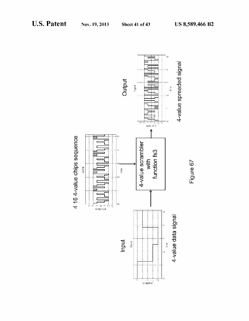
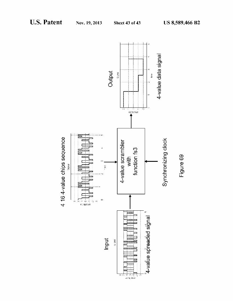
descramblers as signal spreaders and de-spreaders. Spreading and de-spreading of binary signals as known in the prior art of spread spectrum technology is in essence scrambling of a rapidly changing signal sequence (chip sequence) with a much slower changing data signal. De-spreading is the de scrambling of the spreaded signal with a copy of the original rapidly changing signal sequence. n-value Scramblers, com prising one or more of the n-value reversible logic functions, are an excellent way to create n-value spread spectrum digital signals. The application of n-value Scramblers as n-value digital signal spreaders is one aspect of the present invention. As an example, FIG. 67 shows a 4-value spreading appli
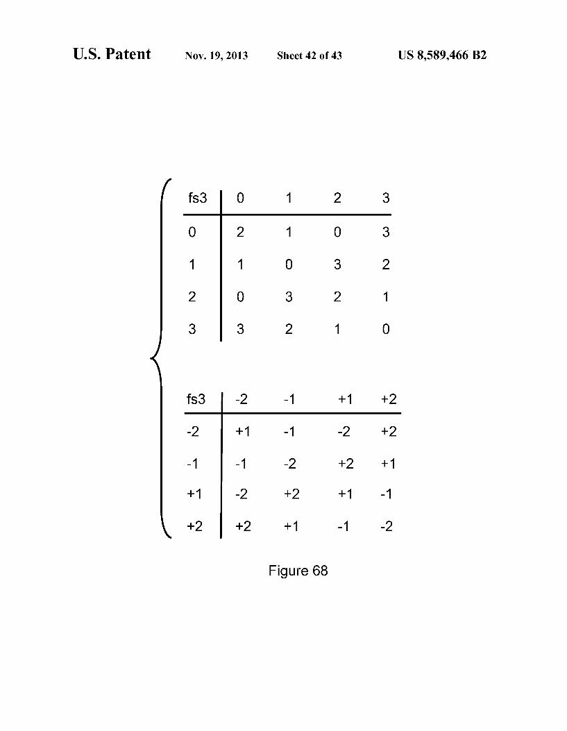
cation by applying the 4-value Scrambling function fis3, as shown in FIG. 68. In order to show the signals as being
US 8,589,466 B2 17
symmetrical, the representation of the 4-value logic States 0, 1, 2 and 3 have been adapted to -2, -1, 1 and 2, as shown in FIG. 68. The spreading application shows how a 4 element 4-value
digital signal is scrambled with a much faster 4-value signal comprising 416 chip digital sequence. The resulting output is the spread 4-value signal.
The recovery or de-spreading of the spread (or scrambled) 4-value signal takes place at the de-spreader or descrambler shown in FIG. 69. Because the 4-value function fis3 that spreads the signal is self reversing, it can be applied in the de-spreader to recover the signal. The diagram of FIG. 69 is similar to FIG. 67. The addition is a synchronizing clock signal that makes Sure that the incoming spread signal and the descrambling 4-value chip sequence are in phase. If these two signals are out of phase, the resulting output of the device is not equal to the original 4-value data signal. Prior art describes several ways to create a synchronizing clock and the Supporting synchronization circuit. One way is to Syn chronize signals with a common pilot signal or derive Syn chronization from the properties of the signal (such as auto and cross correlation). In accordance with one aspect of the invention, n-value descrambling functions applied as n-value digital signal despreaders are used. LFSR Based Multi-Value Scramblers LFSR based multi-value scramblers are contemplated by
the present invention. The binary case will be considered first. FIG. 18 shows the basic configuration of a binary Linear Feedback Shift Register scrambler 350 and its matching descrambler 352. The scrambler 350 in FIG. 18 comprises a shift register having memory elements. A shift register has a series of at least 2 memory elements. Each memory element can contain (in the binary case) the representation of the value 0 or 1. Triggered by an event (like a clock-pulse) the content of each element is shifted one position to its next neighbor, in this case to the right. As long as a memory element contains a value, this value is available as an output signal of the memory element. At least one of the outputs of the memory elements is fed back to the incoming signal. There it is combined with the incoming signal through a two input/single output digital exclusive or device. The output of the exclusive or is usu ally considered to be the scrambled signal. The devices labeled “z’ are XOR devices. The Scrambled signal is then transmitted to the descram
bler 352. It is also fed to a shift register and on the specified event (like a clock pulse) will become the content of the first element of the shift register. The feedback connections from the outputs of elements of the shift register are called taps. In a binary device, taps are connected with each other through an exclusive or (XOR) device. If there is only one tap the feedback tap is connected with the incoming (to be scrambled) binary signal. The number of taps as well as the number of elements (or the length) of a shift register deter mine the statistical characteristics of the scrambled signal. The initial appearance of the scrambled signal is also deter mined by the initial content of the shift register elements. The descrambler is a mirror image of the scrambler as
shown in the above figure. The principles are exactly the same as in the scrambler. The binary descrambler should have a shift register of equal length as the binary scrambler and feedback taps from the elements in the same position as in the related binary scrambler. The connections between the feed back taps are also made through binary exclusive or (XOR) devices. Complete recovery of the signal is possible if the initial content of the elements of the shift register of the descrambler at the start of receiving is the same as the content of the initial content of the shift register of the scrambler.
10
15
25
30
35
40
45
50
55
60
65
18 However after a certain number of steps (having cleared the initial content of the shift register) the descrambled signal will be equal to the original signal no matter what the initial content of the descrambler shift register was.
All LFSR based devices described in this application are governed by a clock signal that will not be drawn or identified in all figures. Such a clock signal is well known. The Ternary LFSR Scrambler/Descrambler Case The canonical lay-out of ternary LFSR scramblers (or
n-value LFSR scramblers) can be the same as the binary form. However, as recognized by the present invention, the applied scrambling functions are different. FIG. 19 illustrates one possible (multi-tap) lay-out of a multi-value LFSR based scrambler 354 based on one aspect of the present invention.
In the ternary case, all memory elements 355 to 359 of the shift register 360 are able to contain 0, 1 or 2 value or state representations. An n-stage LFSR ternary Scrambler can have a maximum of n feedback taps and a maximum of (n-1) devices to connect the taps and one final device (named Op scr) to connect the incoming ternary signal with the feedback (or the result of the feedbacks). The devices that connect the output of a shift register element with a previous result (or in the case of the last tap with another element output) are named Lifsr functions with a number added to indicate different functions. The device that combines the incoming digital data signal
with the feedback from the LFSR and has as output the input to the first stage of the shift register is called Op-scr. The multi-value LFSR based descrambler 362, illustrated
in FIG. 20, has a lay-out (but not always the functions) that is the minor image of the scrambler 354. This is shown in FIG. 20 which illustrates a descrambler that can descramble a signal created by the scrambler of FIG. 19. We will maintain a similar naming convention in the multi
value LFSR based descrambler in FIG. 20. The device that combines the incoming (scrambled) signal with the feedback from the LFSR and has as output the recovered original data signal is called Op-des. All other functions are called Lifsr with a number added to indicate different functions.
For an LFSR system to form a ternary LFSR based scram bling/descrambling system it has to comply with the follow ing requirements and design rules:
First, the shift register in scrambler and descrambler are of equal length. The elements or stages of a shift register are memory elements. In a n-value logic they can contain values that range from 0 to n-1.
Second, Scrambler and descrambler have identical tap con figurations.
Third, the functions Op-scrand Op-des have to be a revers ing pair (one is a scrambling and the other one is a descram bling function. The placement in the scrambler or the descrambler does not matter. But if one is in the scrambler the other has to be in the descrambler). The functions Op-scrand Op-des can also be equal if self-reversing.
Fourth, the functions Lifsr can be any of the reversible ternary functions formed from the ternary reversible invert CS.
Fifth, a selected Lifsr function at a certain tap in the scram bler should correspond with the same function at the corre sponding tap in the descrambler. In case of non-commutative functions, the order of inputs to the devices in scrambler and descrambler configurations should be the same.
Sixth, the initial content of the scrambler and descrambler shift register should be identical. One form for an LFSR based scrambler/descrambler set
would be a scrambler that only applies one commutative self-reversing function for Lifsrand Op functions. In that case,
US 8,589,466 B2 19
the ternary scrambler and descrambler would contain the same elements. The modulo-n addition function does not meet the criterion of being self-reversing for n being an inte ger greater than 2.
Another ternary LFSR scrambler/descrambler set can 5 apply a mix of commutative ternary self-reversing functions for Lifsr and Op-functions. Another ternary LFSR scrambler/ descrambler set can apply a mix of commutative and non commutative functions for Lifsrand Op-functions. The statis tical performance of the ternary LFSR scrambler is determined by the length of the shift register and the number of taps as well as where the taps are placed and what functions are used.
Proper Scrambling/descrambling performance is deter mined by complying with the above stated design rules. 15 The N-Value LFSR Scrambler/Descrambler The design rules can be expanded to the more general
n-value case for LFSR scrambler/descrambler systems. First, both n-value LFSR scramblers and descramblers
should have shift registers of equal length. Each element is able to preserve as its content the representation of the values 0, 1, 2 ..., n-1.
Second, scramblers and descramblers should have identi cal number offeedback taps at corresponding elements of the shift register.
Third, connecting devices should all be reversible n-value functions constructed from n-value reversible inverters.
Fourth, the functions Op-scr and Op-des have to be a reversing pair (one is a scrambling and the other one is a descrambling function. The placing in either scrambler or descrambler does not matter. But if one is in the scrambler the other has to be in the descrambler) Or the functions Op-scr and Op-des are equal if self-reversing.
Fifth, the functions Lifsr can be any of the reversible multi value functions formed from the multi-value reversible inverters.
Sixth, a selected Lifsr function at a certain tap in the scram bler should correspond with the same function at the corre sponding tap in the descrambler. In case of non-commutative functions the order of inputs to the devices in scrambler and descrambler should be the same.
Seventh the initial contents of the shift register in scrambler and descrambler should be identical for complete recovery of the original signal.
FIG. 21 illustrates one example of an n-value LFSR based 45 scrambling system in accordance with one aspect of the present invention. FIG. 21 shows a diagram of a 4-value 5-stage LFSR based scrambler and its matching descrambler applying only devices with the self reversing functional truth table scrá d, as shown in FIG. 17.
FIG. 21 illustrates another example of an n-value LFSR based scrambling system in accordance with another aspect of the present invention. FIG.22 shows a diagram of a 4-value 5-stage LFSR based scrambler and its matching descrambler applying devices with the self reversing functional truth 55 tables scrá a, scra c and scra das shown in FIG. 17. Spe cifically, functions S and D implement scrá d, function L1 implements scra a and function L2 implements scra c, as shown in the figure. Not all self reversing multi-value functions are commuta- 60
tive. Another example of an n-value LFSR based scrambling system is shown in FIG.23. Here, one of the functions applied as the connecting device between incoming input and feed back from the shift register is a non-commutative self-revers ing 4-value function, Scrag. Because function scrag is self 65 reversing it is also applied in the position corresponding with Op-des in the descrambler. The truth table of the 4-value
10
25
30
35
40
50
20 self-reversing function scra g is shown in FIG. 24. Note that the order of the inputs to the table of scra g is important to determine the output (the inputs cannot be switched) so that the function is non-commutative. Not every commutative reversible n-value function is self
reversing. FIG. 26 shows the application of the reversible and commutative 4-value function scra e in a 4-value 5-stage LFSR based scrambler. This function is applied in the posi tion of Op-scr. Consequently the matching function Op-des in the descrambler should be the reverse of Op-scr. This reverse is the non-commutative, reversible function scra f. The truth tables of scrae and scra fare shown in FIG. 25.
Prior art mentions multi-value LFSR based scrambling and descrambling but often in a cursory way, indicating a belief that multi-level LFSR based scrambling and descrambling is an extension of the binary form and displaying a limited understanding of the rules for n-value LFSR based scram bling and descrambling. As illustrated herein, multi-level LFSR based scrambling and descrambling is not a simple extension of the binary rules. One reference the inventor found to a related approach was
in the Help Pages of Mathworks Simulink Communication Blockset on Feb. 12, 2004, found on the internet. These pages describe an algorithm for n-value integer signals for LFSR based scramblers and descramblers. The help file on the web site described a set of LFSR based scramblers/descramblers that strictly apply modulo-n adders. This is appropriate for binary application. However if all applied functions (in the scrambler as well as the descrambler) as described by Math works are modulo-n addition the descrambler can in the described form not recover the original signal. This approach does not work to make ternary and multi-value LFSR scram blers/descramblers, and fails to recognize that modulo-n addition (with n greater than2) is not a self reversing function.
Another example in prior art mentions modulo-n Subtrac tion as the descrambling function for Scrambling by modulo-n addition. Such an observation is not specific enough. Modulo-n addition can be implemented with an n-value commutative function. However Subtraction is non commutative. That means that if the order of inputs to an n-value subtraction is switched at the descrambler, the recov ered signal in case of n-value (n greater than 2) is not the original signal. Conversely modulo-n Subtraction is a set of two n-value logic functions.
Another observation is that modulo-n subtraction is a self reversing but non-commutative function in n-value logic. This has an interesting consequence for n-value Scramblers (be it with or without LFSR). If an n-value scrambler, such as in FIG. 19, has n-value subtraction as n-value function Op scr, it can have the same n-value Subtraction function as Op-des in the descrambling function as shown in FIG. 20. because the subtraction function is self reversing. However the descrambler as shown in FIG. 20 can also have the func tion modulo-n addition as Op-des function.
Consequently the rules as described in this application provide rules that state a set of conditions that will ensure that scramblers and descramblers that comply with the rules will demonstrate complete recovery of scrambled multi-value sig nals. The set of rules may not be exclusive. There are other combinations of n-value functions possible that also show scrambling/descrambling capabilities. The inventor believes he is the first to have invented meth
ods for creating LSFR ternary and multi-value scramblers and descramblers. He also believes he is the first to be able to articulate and design different matching sets of multi-value LFSR based scramblers and descramblers.
US 8,589,466 B2 21
It should be clear that because many reversible possible functions can be applied there is a large range of possible n-value logic LFSR scrambler/descrambler combinations. n-Value LFSR Based Scramblers/Descramblers as n-Value Signal Spreaders/Despreaders 5 The n-value LFSR based scramblers and descramblers can
be used as single channel or single user n-value spreader and despreader. The present invention contemplates at least two different spreader/despreader realizations. These include an N-value LFSR based spreader/despreader with no synchro nization and an N-value LFSR based spreader/despreader with Synchronization. N-value LFSR Based Spreader/Despreader with No Synchro nization
In this configuration an n-value LFSR based scrambler is applied to Scramble an incoming n-value data signal. The scrambler operates on a clock signal. The clock signal is significantly faster than the maximum rate of change of the n-value data signal. Each element of the n-value digital data 20 input signal to the Scrambler is assumed to have a constant duration. The number of clock pulses during the presence at the input of the scrambler of one n-value data signal element is N. One n-value digital input data signal element will thus be scrambled with N. chips. The result is a scrambled signal 25 with N elements. N is called the spreading factor.
The configuration of this set-up uses the LFSR based n-value scrambler to generate the spreading chip-sequence as well as to create the Scrambled sequence.
The despreading part of the invention is the matching 30 n-value LFSR based descrambler to the previous scrambler operated at the same clock frequency. Because the descram bler is self-synchronizing there is no requirement for deter mination of the starting position of the received scrambled sequence. The descrambler may become temporarily desyn- 35 chronized. As soon as the shift register is flushed the descrambler is synchronized again.
It may be required to synchronize the clock signal of the receiving descrambler with the incoming scrambled signal in order to ensure optimal signal level detection. 40 A diagram of the N-value LFSR based spreader/despreader
in accordance with one aspect of the present invention is shown in FIG.55. FIG.56 shows the truthtable of applied self reversing ternary function sc2. The representation of ter nary data input signal and the resulting spreaded signals by 45 the invention are shown in FIG. 57. The spreading factor (26 in the example) is determined by the frequency of the clock signal. The statistical characteristics of the spreaded signal are determined by the configuration of the LFSR based scrambler. 50
The configuration of the scrambler as shown in FIG. 55 generates a ternary m-sequence for input data signal '0'. The auto-correlation for the spreaded signal is shown in FIG. 58. The auto-correlation of the spreaded ternary signal 1 is shown in FIG. 59. The auto-correlation adjusted by applying 55 one of the reversible ternary inverters on the received signal is shown in FIG. 60. The adjusted auto-correlation with a dif ferent ternary inverter for spreaded digital data signal 2 is shown in FIG. 61. The autocorrelation has 3 equal peaks within period 2 N-1 and is not well suited for signal syn- 60 chronization. By application of the self-synchronizing descrambler no further synchronization should be required. N-Value LFSR Based Spreader/Despreader with Synchroni Zation
FIG. 62 shows a spreader/despreader system that applies 65 the same n-value spreading sequence generated by an n-value LFSR based sequence generator. In the figure as an example
10
15
22 a 4-stage ternary LFSR, using ternary function Sc4 is applied. FIG. 63 shows the truth table for ternary function sc4. The LFSR in FIG. 62 works independent of the incoming
ternary data signal Sigin. The output of the LFSR based sequence generator (the spreading sequence) is scrambled with the incoming ternary data-signal Sigin by a ternary scrambling/descrambling device with truth table sc9. The truth table of sc9 is shown in FIG. 64. Because the rate of change in the spreading sequence is greater than the input data signal, the data signal will be spread. The despreader applies almost the same configuration as
the spreader. The only difference is the descrambling func tion, which is “ds9 or the inverse (or reverse) of sc9. The truth table of “ds9 is shown in FIG. 65. The sequence generator of the despreader again works
independently of the incoming signal. The incoming signal to the despreader function “ds9 is the spread signal. If the spread signal and the spreading sequence are descrambled while in the right synchronization, the result of the descrambling will be the original data input signal. The advantage of this arrangement is that just one spread
ing sequence is required. Each of the three different ternary input signals will create a different spreaded sequence.
There are several basic ways to synchronize the spreading sequence at the despreader with the incoming spreaded sig nal. The best known way of synchronization is to apply a spreading sequence that has a single sharply defined correla tion value.
In this example there are three different sequences, origi nating from the same spreading sequence. In many cases, there are sequences, such as in this example, where each ternary input signal spread by the spreading sequence creates a spread signal that has identical ideal cross-correlation with the spreading signal. This is shown in FIG. 66. By applying ternary reversible inverterias shown in FIG. 11 to the incom ing spread signal, the cross-correlation for all three possible spread signals will be as shown in FIG. 66. This is an advan tageous correlation graph, as it has just one large peak at the same location. This allows for easy detection of synchroni Zation of the incoming signal with the LFSR based sequence generator, without having to distinguish for original input data signal. Inverter Use for Adjusting Cross Correlation
Each individual reversible n-value inverter can be used as a “simple scrambler, inverting selectively elements from an incoming digital n-value signal. Though this does not signifi cantly change the statistical make-up of an n-value digital signal, it can change the appearance. It can also be fully reversed. It is possible to put several inverters consecutively behind each other such that the input of the next one is the output of the previous one.
Another application for using the inverters in an n-value digital signal consisting of 2 or more elements is incomparing two n-value digital sequences by calculating their cross cor relation. In some cases the calculated cross correlation between two digital n-value signals consisting of a sequence of more than 1 element will be a value not equal to zero. In applications it may be advantageous to be able to change signals such that their cross-correlation is Zero while being able to recover the original sequence. A simple way to achieve this is to apply one or more reversible inverters to one or both of the signals, calculate the cross correlation and recover the original signals by applying the inverters in reverse order.
Another application of reversible n-value inverters is that it changes the appearance of the cross-correlation or auto-cor relation in Such a way that one clear peak exists that is sig
US 8,589,466 B2 23
nificantly different from other values. The existence of such a distinguishing peak allows for synchronization of the signal. Generating n-Value Digital Sequence Signals
There are many applications in digital telecommunications where the availability of binary or multi-value digital signals consisting of a sequence of binary or multi-value digital sig nals is desirable or beneficial. For instance the availability of certain binary sequences with particular auto-correlation and/ or cross-correlation properties is critical to the appropriate functioning of spread-spectrum communication applications. More specifically multi-user systems require specific cross correlation properties in wireless applications. One expectation is often that the sequence signal has the
appearance of being statistically random. Linear feedback shift registers are used to create this type of sequences which are known as Pseudo-noise (PN) or pseudo-random noise. These sequences may have the appearance of being random, however, they are fully deterministic in how they are created and what their characteristics are. The terms digital multi-value sequence and signal can be
interchanged in this application. The theory of creating pseudo-random sequences is well
established and there are well defined rules how to create sequences (binary as well as multi-value). As far as the dis closed prior art is concerned: n value sequences appear to be strictly generated by LFSRs with feedback taps comprising modulo-n adders and modulo-n multipliers. One aspect of the present invention is focused on generat
ing n-value (such asternary) sequence signals by applying the previously defined reversible n-value functions, constructed from the set of n-value reversible inverters without use of multipliers. As such, this is a new invention that has not been disclosed in prior art. It allows for replacing the theoretically combination of adders and multipliers with single multi value digital function devices. It also can generate additional sequences with attractive properties such as cross-correlation and auto-correlation that cannot be generated by application of modulo-n addition and modulo-n multiplication.
In prior art pseudo-random number (PN) generators (be it binary or multi-value (n-value)) are Linear Feedback Shift Registers with feedback taps connected to Modulo-n adders. Further more for optimal statistical performance, Some taps will contain modulo-n multipliers in the n-value case (n a positive integergreater than 2) to comply with the coefficients of calculated irreducible polynomials over the Galois Field GF(n).
In accordance with one aspect of the present invention, n-value sequences are generated by new inverter-based, reversible n-value functions (with exception of the modulo-n adder). This aspect of the present invention offers a new and more efficient way to generate n-value sequences. PN generators are in fact scramblers with any input from
the outside combined with the feedback from the LFSR through a function that is constructed from strictly identity inverters. This is demonstrated in its binary form in FIG. 27. The first diagram in FIG. 27 shows a binary 5-stage, 2-tap
scrambler with inputs all 0. This scrambler can be replaced with a configuration as shown in the second diagram of FIG. 27. The device labeled as “..+’ is an XOR device.
There exist two reversible binary inverters as shown in FIG. 28. The first inverter in FIG. 28, i, is the identity, the second inverteri is what is generally recognized as an inverter in that '0' is transformed to 1 and 1 is transformed to 0. By replacing the XOR device, +, that connects the incom
ing signal with the feedback from the LFSR with the identity device, i, a binary Scrambler can be turned into a PN genera tor. The input signal does not influence the outgoing signal
5
10
15
25
30
35
40
45
50
55
60
65
24 out. This new circuit is illustrated in FIG. 29. FIG. 30 shows the truth table for the binary identity. Generalized n-Value Sequence Generators
All multi-value or n-value digital LFSR pseudo-noise gen erators can be treated as n-value LFSR scramblers with the operational connecting device between the incoming signal and the feedback signal being the non-commutative n-value identity function.
It is the object of this invention to create devices and methods that can generate n-value (with n an integer greater than 2) sequences, applying n-value scrambling functions, n-value inverters and n-value shift registers, without regard for the statistical properties of the sequences. Prior art describes ways to determine LFSR based n-value pseudo noise sequence generators by applying irreducible polynomi als over the Galois Field GF(n) and realizing these with modulo-n adders, modulo-n multipliers and n-value shift reg isters.
It is an object of this invention to provide a method to realize prior art n-value LFSR based noise generators and others with functions and devices of this invention.
Prior art LFSR based n-value pseudo noise generators per tain to values of n which are positive integer and prime (e.g. 2, 3, 5, 7, ...). The realized n-value LFSR generators comprise taps containing a multiplier p at one input of the modulo-n adder and multiplier q at the other (with p and q an integer smaller than n). FIG. 31 shows an example of such a generic n-value LFSR based sequence generator. The entities p and q are modulo-n numbers that multiply
the input to the modulo-n adder with. The value of p and q can be determined from the irreducible polynomials over GF(n). If n is a prime integer then the multiplying factors (in this case p and q) are reversible inverters.
FIG. 32 shows the possible inputs to a modulo-3 adder, multiplied with 1 and 2 modulo-3. Multiplying a ternary input with 1 internary logic is the same as inverting the input with the identity inverter. Multiplying a ternary input with a factor 2 internary logic is the same as Subjecting the input to the self-reversing inverter i.
FIG. 33 shows the possible inputs to a modulo-5 adder, multiplied with factors 1, 2, 3, and 4 modulo-5. In 5-value logic, multiplying the input with an integer modulo-5 is the same as Subjecting the input to a reversible inverter (including the 5-value identity). In general: multiplying the input to an n-value digital device is similar to Subjecting that input to an n-value digital reversible inverter. Modifying the Truth Table by Modifying the Input to an n-Value Digital Device
Modifying the input to an n-value digital logic device, characterized by an n-value logic truth table, is the same as not modifying the input, but modifying the characterizing truth table (and thus the function) of the device. This is illus trated in FIG. 34 with a diagram of a ternary (or modulo-3) adder with inputs In 1 and In 2 and output Out. The input In 1 is multiplied by a factor 2. The inputs to the modulo-3 adder are In 1 mod and In 2. In 1 mod is created by multi plying the input In 1 with a factor 2.
FIG. 35 shows the truth table of the modulo-3 adder. The top row of the ternary truth table represents the possible values for input In 1 mod. The left column of the ternary truth table represents the possible values for input In 2.
If the input In 1 is 0 the modulo-3 adder also sees a zero, as 2x0 is 0. If the input In 1 is 1 the modulo-3 adder sees 2, which is 2x1. As a consequence we can say that instead of the column below input In 1 is 1 (adder without In 1 multiplier) it "sees” the column below. In 1 mod is 2.
US 8,589,466 B2 25
If the input In 1 is 2 the modulo-3 adder “sees the column in the truth table below. In 1 mod is 1. The truth table of the modulo-3 adder with the top input multiplied by a factor 2 is the same as the original modulo-3 truth table modified such that the column under In 1 mod is 1 is replaced by the column under In 1 mod is 2 and the column under In 1 mod is 2 is replaced by the column under In 1 mod is 1.
This is illustrated in FIG.36. The original device of FIG.34 is now replaced with the equivalent device depicted in FIG.36 with inputs. In 1 and In 2 and output Out. The corresponding truth table is also shown in FIG. 36. FIG. 36 shows the equivalent ternary logic circuit for the modulo-3 adder with the top input multiplied by a factor two and the truth table of the equivalent circuit.
FIG. 37 shows the equivalent circuit and its truth table for a modulo-3 adder with the bottom input multiplied by a factor 2. The effect of the multiplication of the bottom input by a factor 2 is the switching of the rows of In 2 is 1 and In 2 is 2.
FIG.38 shows the equivalent circuit and its truth table for the modulo-3 adder with both inputs multiplied by a factor 2. The effect of the multiplication of both inputs with a factor 2 is the Switching of the rows. In 2 is 1 and In 2 is 2 as well as the Switching of the columns for In 1 is 1 and In 1 is 2. General n-Value Inverter Method for Finding Equivalent Truth Tables and Circuits An n-value (reversible) inverter has n different elements.
An n-value inverter transforms the possible input values 0, 1, 2,3,..., n-2, n-1 (with na positive integer) into the possible output values: p, q, r, S. ... t, u with all possible output values also being integers Smaller than n, in Such a way no output value is equal to another output value. The transformation is shown in the FIG. 39. The effect of a reversible inversion onan n-value truth table
is:—if the inversion is applied to the top input the column under input is 0 is replaced with the column under input is p. the column under input is 1 is replaced by the column under input q, the column under input is 3 is replaced by the column under input is S. Up to the column under input is (n-1) is replaced by the column under input is u.
If the inversion is applied to the bottom input, the same rules are applied to the rows of the truth tables. If an inversion is applied to both inputs, the above rules apply to columns and rows, and are not dependent on the order of execution.
This method fulfills the object of the invention to create n-value digital logic functions and circuits that can generate not only n value signal sequences, but also all sequences that can be created with prior art but with fewer component func tions applied, as this makes the multipliers obsolete.
In ternary logic, 5 different reversible inverters exist that are different from identity. But there is just one modulo-3 multiplication not equal to 0 or 1. Consequently the inverter based method can generate more different functions than modulo-3 arithmetic and provide a much greater diversity in functions and devices than prior art applying modulo-3 arith metic. The same reasoning and diversity advantage applies to
higher value generation of sequences. The Ternary LFSR Sequence Generators The literature describes a 3-value digital PN generator to be
a LFSR able to contain 3-valued numbers with feedback taps into modulo-3 adders. The feedback taps contain modulo-3 multipliers. The behavior of the ternary pseudo noise genera tor is determined by the number of taps and the values in the multipliers. Literature and prior art describe how to apply irreducible polynomials to design n-value noise generators. One aspect of the present invention comprises ternary or
3-value sequence generators formed from a 3-valued shift
10
15
25
30
35
40
45
50
55
60
65
26 register with feedback taps leading into connecting devices which have describing ternary truth tables comprised of col umns or rows which are selected from the set of 6 reversible ternary inverters. A ternary sequence generator can be any of the possible ternary LFSR scramblers with no input and the connecting device between LFSR signal and input signal being replaced by a short circuit. FIG. 40 shows an example of such a ternary PN generator.
Several terminals can be selected for collecting the output signal. In fact any of the inputs or outputs of the elements of the shift register will do. The output on these terminals will differ on the first output signals as the shift register is being flushed. In general the initial state should be such that transi tions will be generated. The two irreducible polynomials for a 4-stage LFSR based
ternary PN generator with two feedback taps as shown in FIG. 40 are: (x+x+2) and (x+2x+2). Literature says that these two (modulo-3 adder based) solutions are able to generate what is known in prior art as ternary m-sequences. The performance or desirability of a sequence is frequently
measured by correlation and autocorrelation. Auto-correla tion and cross-correlation are important indicators of certain qualities of digital sequences. The Subject of auto-correlation is well documented. Correlation is usually calculated between two sequences. In auto-correlation the second sequence is a copy of the original one.
In principle, correlation of two sequences of equal lengths (assume length is n elements) is calculated by multiplying the assigned value of the k" element of the first sequence with the assigned value of the k" element of the second sequence. This multiplication is done for all n elements of both sequences. The result of these multiplications is added into one sum. This Sum is then called the correlation value. In general, the cor relation between two sequences is calculated for all time shifted instances of one of the sequences. If the length of the sequences is n elements, there will be 2n-1 different matches between two sequences of length n. The graph that displays the 2n-1 correlation values
between the two sequences is in general called the auto correlation graph (if the two sequences are equal) or the cross-correlation graph if the correlation is determined between two different sequences of equal length.
M-sequences or maximum length sequences in the binary case are sequences that have an autocorrelation value A in all time shifted calculations and a value B when a sequence is correlated with a non-shifted copy of itself. The value of A and B depends on the assigned value to the binary elements. In case of a balanced assigned value (say 0 is assigned the value -1 and 1 is assigned the value +1) the value of A can be 0. It is well known that sequences with certain auto- and cross-correlation have attractive properties. One aspect of this invention determines configurations to generate ternary and n-value sequences with m-sequence like properties. It is pos sible to normalize correlation calculations for n-value sequences with n an integer greater than 2. In general, for calculating correlation properties of an in value digital signal will be considered having the values: 0, 1, 2, 3,..., n-1. For calculating the correlation, these values will be used or these values will be substituted so they are balanced around 0, (for instance by subtracting (n-1)/2 of all values if n is odd; and by substituting the first n/2 states with -(n/2)+i for i=0, 1, . . . (n/2-1) and the next n/2 states with i-(n/2-1) for i=n/2,..., n-1 if n is even). The above type of substitution does affect the individual correlation values but not the shape of the correla tion graph. However, the substitution can also reflect use of different reversible inverters. This can change the overall
US 8,589,466 B2 27
shape of the correlation graph, mainly the orientation of some of the peak values in the correlation graph as being above or below the average line. One measure for the performance or desirability of a
sequence is its autocorrelation. The modulo-3 adder with multipliers provides 2 configurations for generating m-se quences based on the irreducible polynomial in the lay-out of FIG. 40. The application of reversible ternary functions can provide at least 6 different configurations under the lay-out of FIG. 40 that will generate m-sequences. This invention in general provides greater diversity with fewer components to generate attractive n-value digital sequences.
FIGS. 41,42, 43, 44, 45 and 46 show the truth tables of the applied different ternary devices in the lay-out of the sequence generator as in FIG. 40 for the LFSR based ternary m-sequence generator and a graph of the auto-correlation of the generated sequences.
The autocorrelation graphs show that applying the func tions ter1, ter2, ter5, ter6, ter9 and ter10 in the ternary 4 stage LFSR with taps on the output of the3" and 4"element creates sequences with attractive properties. One reason they are attractive is because they will make it easier to determine synchronization. Analysis of the sequences will show that the shifted sequences are not equal to each other. This indicates that the thus generated individual shifted sequences also have very attractive orthogonal properties.
For illustration purposes, FIG. 47 showing the autocorre lation and truth table for the above sequence generator ter3 has been included. The application of this function demon strates much less attractive properties. This is because it will be difficult to detect a peak value where synchronization OCCU.S.
The n-Value Digital Sequence Generators The above reasoning can be extended to all multi-value or
n-value (with n an integer greater than two) linear feedback shift register based digital sequence generators.
Thus, one aspect of the present invention provides a n-value (with nan integer greater than 2) sequence generators formed from n-value Linear Feedback Shift Registers with a maximum number of n feedback taps connected by n-value logic function devices of which the truth tables are con structed from n-value reversible inverters. These systems have no input signal. The resulting feedback is directly guided to the first stage of the shift register.
The inventor has tested the sequences generated by the different configurations depicted in FIGS. 41, 42, 43, 44, 45 and 46. While the sequences generated by each configuration are time shifted, the sequences of each configuration are totally different from the sequences generated by the other configurations. Consequently this invention can generate a greater set of m-sequences than prior art by nature of its greater set of connecting multi-value functions or devices than in prior art.
Exceptions to this invention are any LFSR system that contains only modulo-n adding devices as two-input connec tors in LFSR based sequence generators. These modulo-n adding devices based systems are prior art. Adjusting Auto-Correlation and Cross-Correlation of Sequences The auto-correlation of an n-value digital sequence can be
considered to be cross-correlation between this sequence and a time shifted version of this sequence. It is useful to have a cross-correlation or auto-correlation that is Zero over as large a period as possible. The ternary LFSR based sequence generator as shown in
FIG. 46 applying ternary function ter10 has an auto-corre
10
15
25
30
35
40
45
50
55
60
65
28 lation value of-1 over a large area, with low peaks with value 26 at n=4.0 and n=120 and a large peak of value 53 at n=80.
It would be useful to be able to change the auto-correlation Such that is has just one positive peak for synchronization. It would also be very beneficial if the cross-correlation between time shifted sequences could be made 0 (which means that these sequences are orthogonal). By applying ternary inverter is as shown in the table of
reversible ternary inverters in FIG. 11 to the sequence after generating the sequence but before determining the auto or cross correlation, the correlation is adjusted to 0 over the majority of the sequence period. Further, the peak value is adjusted to -54 at n=4.0 and at n=120 and to +54 at n=80.
FIG. 48 shows a graph of the adjusted auto-correlation for the LFSR based ternary sequence generator with lay-out as in FIG. 40 with device ter10 and applying ternary reversible inverter is to the sequence before determining the correlation.
In accordance with another aspect of the present invention, the level of the cross-correlation of two n-value digital sequences can be adjusted by applying one or more similar or different n-value inverters to each sequence before determin ing the cross-correlation.
In accordance with a further aspect of the present inven tion, the level of the auto-correlation of an n-value digital sequence can be adjusted by applying one or more similar or different inverters to the sequence before determining the auto-correlation. The auto-correlation is determined by shift ing the original n-value sequence in time (or phase) and calculating the correlation between the original and shifted n-value sequence. Appropriate adjustment can beachieved by applying similar or different inverters to the original and its shifted sequences.
Consequently the invention does not only provide a greater diversity in creating sequence generators it also provides better ways to make use of them.
PREFERRED EMBODIMENT OF THE N-VALUE DIGITAL SCRAMBLERS DESCRAMBLERS, INVERTERS AND SEQUENCE GENERATORS
As many apparently different embodiments of this inven tion may be made without departing from the spirit and scope thereof, it is to be understood that the invention is not limited to the specific embodiments thereof. One embodiment of the execution of the multi-value
scrambling, descrambling and sequence generators is by way of programmable Digital Signal Processors (DSPs). In such an embodiment the incoming multi-value digital signal (in case of a scrambler or descrambler) can be translated by an A/D converter into binary representation and read into the DSP. The DSP can be programmed to execute the scrambling, descrambling and signal generating functionality in binary form and apply a D/A converter to create the multi-value digital output signal.
Another embodiment of the execution of the multi-value scrambling, descrambling and signal generating functionality is by way of binary logic and binary or hybrid memory ele ments. Multi-value digital signal inputs can be translated through an A/D converter into binary representation. The ternary and multi-value logic functions can be contained in electronic memory devices in Such a way that the binary representation of the input signals form the addresses of memory locations. The content of the memory devices at these locations then form the result of the truth table repre senting the ternary and multi-value logic functions, also in binary form. The content of the specific memory address location can be used for further processing or can be trans
US 8,589,466 B2 29
lated from binary form into a ternary or multi-value signal by using a D/A converter. Consequently multi-value shift regis ters in LFSR applications can be either clocked binary memory devices. They can also be analog or hybrid devices where the content of a memory location is a physical entity (such as electrical charge) representative of the value of a ternary or multi-value signal.
Another embodiment of the execution of the multi-value scrambling, descrambling and signal generating functionality is by way of complete discrete binary logic. A new embodiment ofternary and multi-value Scrambling,
descrambling and signal sequence generating execution is the application of existing and emerging ternary and multi-value electronic logic circuits either in CMOS or otherwise. A method to design the embodiment internary and multi
value electronic form is part of this invention. It is shown for ternary logic but can easily be visualized in any higher value logic. The object is to realize any ternary two inputs/single output
truth table internary logic. The assumption is that the follow ing two electronic elements are available: The first element is an electronic gate that conducts a currentifa control input has a value equivalent to a state '0'. The gate is non-conducting for all other control values. This gate is shown in conducting state in FIG. 49 and in non-conducting state in FIG. 50. It is assumed that the gate is direction sensitive and should be read from left to right. The second element is a universal ternary inverter equiva
lent to ternary inverteria or is. Applying inverteria twice acts like applying is. Applying ternary inverter is twice acts like applying ternary inverter i once. Applying inverter i fol lowed by inverter is is the same as identity. Applying inverter is followed by inverter i is also like applying identity. Also applying is three times as well as applying is three times is equal to identity.
FIG. 51 shows the result of applying ternary reversible inverteria twice. FIG. 52 shows the effect of applying ternary reversible inverter is twice. The number columns between the vertical lines in FIG. 51
and FIG. 52 represent possible states before and after inver Sion. It should be clear that by applying one inverter once or twice each initial ternary state can be transferred to each desirable other ternary state.
With the gate and universal ternary inverter (ioris) as only available components (but in unlimited amounts), every pos sible ternary two-input single output device can be realized. To demonstrate this, the ternary truth table shown in FIG. 53 will be realized in diagram by applying the gatefuniversal inverter method.
FIG. 54 shows a diagram of a device realizing the ternary truth table exclusively with the gate and ternary universal inverter is as components. The electronic device 370 has two inputs 371 and 372. The signal b is input to the first input 271 and the signal a is input to the second input 372. The elec tronic device 370 also has three channels 373,374 and 375.
Each channel in this case corresponds with the realization of a column of the truth table. The empty circles indicate the inverter is. The circle 385 with a line inside shows a gate controlled by an input 386. If the state of the control input to the gate 385 is 0, then the gate is conducting and signals are passed from the input 387 to the output 388. If the state of the control input to the gate 385 is not 0, then the gate 385 is not conducting and no signals are conducted from the input 387 to the output 388.
The electronic device 370 also has an output 381. If a=0, then state 0 is applied to gate 376 so that gate 376 is
enabled so that the first channel 371 conducts, and input 371
10
15
25
30
35
40
45
50
55
60
65
30 is connected to output 381. In this case, gates 378 and 380 have a non-0 state applied from the input signal 'a' at input 372. In case of gate 378, the input state 0 is provided to the input of the inverter is in the control input of gate 378. The inverter transforms the provided input state to the state 2 which is the control input state to the gate 378, which is thus not conducting. In the case of gate 380, the input state 0 is provided to the input of the first inverter is in the control input of gate 380. The inverter transforms the provided input state to the state 2 which is then the input state to the second inverter is in the control input of gate 380. The second inverter transforms the provided input state 2 to the state 1 which is then the input state to the control input of gate 380, which is thus not conducting. Thus, the channels 374 and 385, respec tively, do not conduct, and cannot contribute to the signal at output 381. Only signals through channel 373 contribute to the output signal at output 381. A signal coming from input 371 going through 378 to
output 381 is transformed by the inverter is 389 in its path. So if a=0 and b-0 then the state of the signal b=0 is transformed to state 2 and output 381 assumes the state 2. If a=0 and b=1 then the state of the signal b=1 is transformed to state 0 and output 381 assumes the state 0. If a=0 and b=2 then the state of the signal b=2 is transformed to state 1 and output 381 assumes the state 1. These states represent the first column of the truth table of the ternary logic function ternary as shown in FIG.S3.
If a=1, then only gate 378 conducts. Gates 376 and 380 are non-conducting. Then one of the gates 382, 383 or 384 will conduct, depending on the value of the input b. If b=0, then gate 382 will conduct and the subchannel 390 is conducting. Subchannels 391 and 392 are non-conducting. The signal representing b–0 will be inverted by inverter is in subchannel 390, and the output will be 2. If b=1, then gate 383 will conduct and Subchannel 391 is conducting. In this case, Sub channels 390 and 392 are non-conducting. The signal repre senting b=1 will be inverted by inverter i5 in subchannel 391 and the output will be 0. Ifb=2 then gate 384 will conduct and the subchannel 392 will be conducting. Subchannels 390 and 392 will be non-conducting. The signal representing b–2 will be inverted twice by the inverters is in subchannel 392, first from 2 to 1 and then from 1 to 0 and the output will be 0. The output states represent the second column of the truth table of the ternary logic function ternary as shown in FIG. 53.
If a=0 then only gate 380 conducts. Gates 376 and 378 are non-conducting since a non-Zero value is applied to the con trol input of these gates as a result of the inputa. In this case, the output of the electronic device 370 is 0 when the input b is 0, 1 when the input b is 1 and 2 when the input b is 2. These states represent the third column of the truth table of the ternary logic function ternary as shown in FIG. 53.
Similar embodiments with components employing a gate that conducts if the control input is 0 and a reversible n-value inverter would be able to realize any n-value digital logic function. Thus, any of the n-value logic functions defined herein can be constructed. The reduction of combinations of n-valued inverters at
inputs of n-valued logic functions have been disclosed in accordance with one aspect of the present invention. Examples have been provided and FIGS. 31-38 highlight elements of the reduction. The methods as provided apply to all n-valued 2 input/single output functions. They will also apply in essence to functions with more than 2 inputs. The method has been demonstrated for any n>2 and any GF(n). In general the reduction method will be used for LFSRs which initially may be derived from irreducible polynomials over GF(n). It has been shown as another aspect of the present
US 8,589,466 B2 31
invention that LFSRs can use reversible n-valued logic func tions that can not readily be derived from Such polynomials. The truth tables of functions may be created from n-valued reversible inverters as rows and/or columns of the truth table.
Appropriate n-valued logic functions for LFSRs cannot be created from truth tables of modulo-n adders (which are reversible) with modulo-n multipliers if n can be factorized, such as n=4. n=6, n=9, etc, or in other words if n is not prime. A known method to create a field over GF(n) if n is not prime, but n u?, whereinu is a prime number and pa2, is to create an extended field GF(u?). It is known that in order to define an extended field GF(u) one will use a primitive polynomial over GF(u) to define the extended field. Within the extended field a reversible multiplication exists and a reversible addi tion. According to the method explained earlier, the constant multipliers in GF(u?) can be considered as n-valued revers ible inverters with n u?. Accordingly the constant multipliers at inputs of an addition in GF(u) can be reduced to a single reversible n-valued logic function, wherein the truth table of the addition over GF(u?) is modified according to n-valued inverters representing the multipliers over GF(u) at the inputs of the addition function. This means that an expression Z=(rxx)+(qxy) wherein x is a multiplication over GF(u?) and + is an addition over GF(u?), r and q are n-valued con stants and X and y are n-valued variables, can be replaced by an expression ZX Sc4 y, wherein Sc4 is a n-valued logic function. The truth table of sc4 can be created by modifying the truth table of + according to the n-valued inverter repre senting (rxX) and the n-valued inverter representing (qxy). Inverters (rxx) and (qxy) are commutative. An illustrative example will be provided for GF(2).
Assume the expression Z (2xx)+(3xy) over GF(2). This can be replaced by the expression Z(x scay). The following tables provide the truth tables of addition + and multi plication x over GF(2), as well as the truth table of sc4.
-- O 1 2 3 x 0 1 2 3 Sc4 O 1 2 3
O O 1 2 3 O O O O O O O 3 1. 2 1 1 O 3 2 1 0 1 2 3 1 2 1 3 O 2 2 3 O 1 2 O 2 3 1 2 3 O 2 1 3 3 2 1 0 3 O 3 1 2 3 1 2 O 3
It should be clear that the function reduction can be per formed for any expression Z (rxX)+(qxy) over any extended field GF(u?) with u?">2, u2 and pa1. The situation u?=2 is the binary case. The solution for either r=0 or q=0 is trivial. The solution for r=1 provides ZX--(qxy), which will have a func tion Sc4 created by modifying the +truth table according to (qxy) and q=1 will provide Z=(rxx)+y, which will have a function Sc4 created by modifying the + truth table according to (rxX).
In view of the above description of the present invention, it will be appreciated by those skilled in the art that many variations, modifications and changes can be made to the present invention without departing from the spirit or scope of the present invention as defined by the claims appended hereto. All Such variations, modifications or changes are fully contemplated by the present invention.
While the invention has been described with reference to an illustrative embodiment, this description is not intended to be construed in a limiting sense. For example, while the disclosed embodiments utilize discrete devices, these devices can be implemented using one or more appropriately pro
10
15
25
30
35
40
45
50
55
60
65
32 grammed processors, special-purpose integrated circuits, digital processors, or an analog or hybrid counterpart of any of these devices.
The invention claimed is: 1. A device to generate on an output an n-state symbol, the
n-state symbol having one of n states with n>2 and the n-state symbol being represented by a signal, comprising:
a first input and a second input to a memory, each input enabled to receive a signal representing a first and a second n-state symbol each provided by an n-state shift register,
the memory storing a non-commutativen by n n-state truth table not being a modulo-n subtraction; and
an output of the memory to provide a signal representing the n-state symbol in accordance with the non-commu tative n by n truth table.
2. The device of claim 1, wherein n>3. 3. The device of claim 1, wherein the non-commutativen
by n truth table represents a truth table of an addition over a finite field GF(n) modified in accordance with an n-state multiplication over GF(n).
4. The device of claim 1, wherein the non-commutativen by n truth table represents a commutative n by n truth table modified in accordance with an n-state inverter.
5. The device of claim 1, wherein the device is part of a scrambler.
6. The device of claim 1, wherein the device is part of a descrambler.
7. The device of claim 6, wherein the descrambler is self synchronizing.
8. The device of claim 1, wherein the device is part of a generator of a sequence of n state symbols.
9. The device of claim 8, wherein the sequence is a maxi mum-length sequence.
10. The device of claim 1, wherein an n-state symbol is represented by a plurality of binary signals.
11. The device of claim 1, wherein the device is part of a communication system.
12. A method to generate with a processor an n-state sym bol as part of processing a sequence of n-state symbols, each n-state symbol having one of n states with n2 and being represented by a signal, comprising:
the processor storing on a memory device in a coder a non-commutative n by n n-state truth table not being a modulo-n Subtraction;
the processor inputting on a first input of the memory device a signal representing a first n-state symbol;
the processor inputting on a second input of the memory device a signal representing a second n-state symbol; and
outputting on an output of the memory device a signal representing the n-state symbol generated in accordance with the non-commutativen by n n-state truth table.
13. The method of claim 12, wherein n>3. 14. The method of claim 12, wherein the non-commutative
n by n n-state truth table represents a truth table of an addition over a finite field GF(n) modified in accordance with an n-state multiplication over GF(n).
15. The method of claim 12, wherein the non-commutative n by n n-state truth table represents a commutativen by n truth table modified in accordance with an n-state inverter.
16. The method of claim 12, further comprising: processing the n-state symbol in a Linear Feedback Shift
Register (LFSR).
US 8,589,466 B2 33
17. The method of claim 12, further comprising: processing the n-state symbol in a descrambler. 18. The method of claim 12, wherein the n-state symbol is
generated in a sequence generator. 19. The method of claim 12, wherein the n-state symbol is 5
generated in a communication system. 20. The method of claim 12, wherein the n-state symbol is
represented by a plurality of binary symbols. k k k k k
34
UNITED STATES PATENT AND TRADEMARK OFFICE
CERTIFICATE OF CORRECTION
PATENT NO. : 8,589,466 B2 Page 1 of 1 APPLICATIONNO. : 13/027387 DATED : November 19, 2013 INVENTOR(S) : Peter Lablans
It is certified that error appears in the above-identified patent and that said Letters Patent is hereby corrected as shown below:
Title page, item 54 and In the Specifications, Column 1, title should read as follows:
Ternary and Multi-Value Digital Signal Scramblers, Descramblers and Sequence Generators
Signed and Sealed this Eighteenth Day of March, 2014
74-4-04- 2% 4 Michelle K. Lee
Deputy Director of the United States Patent and Trademark Office


![United States Patent [191 [11] Patent Number: 5,389,382 [45] Date … · 2017. 4. 6. · United States Patent [191 List et a1. USOO5389382A [11] Patent Number: [45] Date of Patent:](https://img.pdfslide.net/doc/110x75/60bd3e45b423d52f4d291c3d/united-states-patent-191-11-patent-number-5389382-45-date-2017-4-6.jpg)


![US005398694A United States Patent r191 5,398,694 [45] 21,](https://img.pdfslide.net/doc/110x75/62aad2667a43d35ee34ba83e/us005398694a-united-states-patent-r191-5398694-45-21.jpg)