Embed Size (px)
Citation preview


Model No. : LQ121S1LG84
PAGE
△1 P.6 Error correction
(×)The VCC power … ⇒(○)The VDD power …
P.15
△2 6 Update 【*2】 in 5.Absolute Maximun Ratings
8
9
-
15
(non-operating) is added to vibration test and shocktest.
LD-23301A 2012/12/12
SPEC No.
LD-23301A
LD-23301B
-
RECORDS OF REVISION
NOTEREVISEDNo
DATE SUMMARY
2011/3/5
2012/2/15
Update Timing characteristions
"6.2 LED backlight" Changed VBR active timing (t11)
Added VBR(PWM) regulater values and Remark 【*7】
Delete unnecessary page.
( overlapped page
"7.Timing characteristics of input signals")
Update 10. Handling Precauions
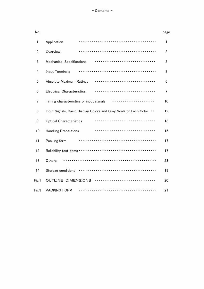
No. page
1 Application ・・・・・・・・・・・・・・・・・・・・・・・・・・・・・・・・・・・・・・・・・ 1
2 Overview ・・・・・・・・・・・・・・・・・・・・・・・・・・・・・・・・・・・・・・・・・ 2
3 Mechanical Specifications ・・・・・・・・・・・・・・・・・・・・・・・・・・・・・・・・ 2
4 Input Terminals ・・・・・・・・・・・・・・・・・・・・・・・・・・・・・・・・・・・・・・・・・ 3
5 Absolute Maximum Ratings ・・・・・・・・・・・・・・・・・・・・・・・・・・・・・・・・ 6
6 Electrical Characteristics ・・・・・・・・・・・・・・・・・・・・・・・・・・・・・・・・ 7
7 Timing characteristics of input signals ・・・・・・・・・・・・・・・・・・・・・・・ 10
8 Input Signals, Basic Display Colors and Gray Scale of Each Color ・・ 12
9 Optical Characteristics ・・・・・・・・・・・・・・・・・・・・・・・・・・・・・・・・ 13
10 Handling Precautions ・・・・・・・・・・・・・・・・・・・・・・・・・・・・・・・・ 15
11 Packing form ・・・・・・・・・・・・・・・・・・・・・・・・・・・・・・・・・・・・・・・・・ 17
12 Reliability test items・・・・・・・・・・・・・・・・・・・・・・・・・・・・・・・・・・・・・・・・・ 17
13 Others ・・・・・・・・・・・・・・・・・・・・・・・・・・・・・・・・・・・・・・・・・・・・・・・・・・ 28
14 Storage conditions ・・・・・・・・・・・・・・・・・・・・・・・・・・・・・・・・・・・・・・・・・ 19
Fig.1 OUTLINE DIMENSIONS ・・・・・・・・・・・・・・・・・・・・・・・・・・・・・・・・ 20
Fig.3 PACKING FORM ・・・・・・・・・・・・・・・・・・・・・・・・・・・・・・・・・・・・・・・・・ 21
- Contents -

LD-23301C- 1
1.Application
This specification applies to the color TFT-LCD module LQ121S1LG84.
This specification is the proprietary product of SHARP CORPORATION (”SHARP) and include materials
protected under copyright of SHARP. Do not reproduce or cause any third party to reproduce them in any
form or by any means, electronic or mechanical, for any purpose, in whole or in part, without the express
written permission of SHARP.
The device listed in this specification was designed and manufactured for use in general electronic
equipment.
In case of using the device for applications such as control and safety equipment for transportation (controls of
aircraft, trains, automobiles, etc.), rescue and security equipment and various safety related equipment which
require higher reliability and safety, take into consideration that appropriate measures such as fail-safe functions
and redundant system design should be taken.
Do not use the device for equipment that requires an extreme level of reliability, such as aerospace applications,
telecommunication equipment (trunk lines), nuclear power control equipment and medical or other equipment
for life support.
SHARP assumes no responsibility for any damage resulting from the use of the device which does not comply
with the instructions and the precautions specified in this specification.
Contact and consult with a SHARP sales representative for any questions about this device.

LD-23301C- 2
2.Overview
This module is a color active matrix LCD module incorporating amorphous silicon TFT (Thin Film Transistor).
It is composed of a color TFT-LCD panel, driver ICs, control circuit, power supply circuit and a White-LED
Backlight unit. Graphics and texts can be displayed on a 800×RGB×600dots panel with about 262144 colors
colors by using LVDS (Low Voltage Differential Signaling) and supplying +3.3V DC supply voltages for TFT-LCD
panel driving and +12.0V DC supply voltage for backlight.
The TFT-LCD panel used for this module is a high-brightness and high-contrast image.
The maximum viewing angle is in the 6o'clock direction.
The 12o'clock direction is difficult to reverse the grayscale.
The LED driver circuit is built into the module.
3.Mechanical technical literatures
(*1) excluding the area of the connector cover.
Outline dimensions are shown in Fig.1.
mm
mm
g
R,G,B vertical stripe
0.3075(H)×0.3075(V)
4:3
Unit
cm
mm
pixel
technical literatures
31(12.1inch)Diagonal
246.0(H)×184.5(V)
800(H)×600(V)
(1pixel=R+G+B dot)Pixel format
Active area
Display size
Parameter
Display mode
Pixel configuration
Pixel pitch
Aspect ratio
Anti-glare and hard-coating 3H
Normally white
Surface treatment
Mass
Unit outline dimensions(*1)
276.0(W)×209.0(H)×9.1(D)
600

LD-23301C- 3
4.Input Terminals
4-1.TFT-LCD panel driving
CN1(Interface signals and +3.3V power supply)
Using connectors: FI-SEB20P (Japan Aviation Electronics industry Co., Ltd.)
Corresponding connectors: FI-SE20M or FI-S20S
(Japan Aviation Electronics industry Co., Ltd.)
Using LVDS receiver: Building into cotroll IC(THC63LVDF84B(Thine electronics) or Compatible product)
Corresponding LVDS transmitter:THC63LVDM83R(Thine electronics) or Compatible product
CN1
Pin1234567891011
GNDRxIN0-
SymbolVccVccGND
RxIN0+GND
RxIN1-RxIN1+GND
R IN2
Remark
GNDGND
LVDS receiver signal CH0 (-)
Function+3.3V Power supply+3.3V Power supply
LVDSLVDS
LVDSLVDS
LVDS receiver signal CH0 (+)GND
LVDS receiver signal CH1 (-)LVDS receiver signal CH1 (+)
LVDSGND
LVDS i i l CH2 ( )11121314151617181920
【*1】 RL/UD = LOW RL/UD = HIGH
NCGND
CK IN+
RxIN2+
CK IN-
RxIN2-
GND
Non Conection
LVDS
LVDS receiver signal CK (-)
LVDS receiver signal CH2 (+)GND
LVDS receiver signal CK (+)LVDSLVDS
GND
LVDSLVDS receiver signal CH2 (-)
RL/UD *1GNDGND GND
GND
CN1 CN1CN1 CN1
LD-23301C- 4
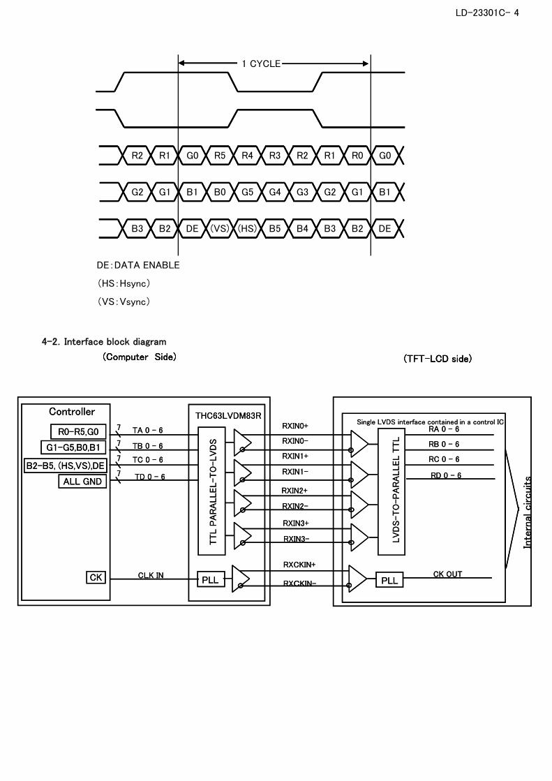
R2 R1 G0 R5 R4 R3 R2 R1 R0 G0
G2 G1 B1 B0 G5 G4 G3 G2 G1 B1
B3 B2 DE (VS) (HS) B5 B4 B3 B2 DE
DE:DATA ENABLE
(HS:Hsync)
(VS:Vsync)
4-2.Interface block diagram
1 CYCLE
(Computer Side) (TFT-LCD side)(Computer Side) (TFT-LCD side)
TC 0 - 6
TA 0 - 6
TB 0 - 6
R0-R5,G0
B2-B5, (HS,VS),DE
G1-G5,B0,B1
RXIN0+
RXIN0-
TD 0 - 6
7
Controller
TTL P
AR
ALLEL-TO
-LV
DS
PLL
THC63LVDM83R
PLL
RXIN1+
RXIN1-
RXIN2+
RXIN2-
RXCKIN+
RXCKIN-CK CLK IN
RXIN3+
RXIN3-
7
7
7ALL GND
Inte
rnal
circuits
RC 0 - 6
RA 0 - 6
RB 0 - 6
RD 0 - 6
CK OUT
LV
DS-TO
-P
AR
ALLEL T
TL
Single LVDS interface contained in a control IC
(Computer Side) (TFT-LCD side)
TC 0 - 6
TA 0 - 6
TB 0 - 6
R0-R5,G0
B2-B5, (HS,VS),DE
G1-G5,B0,B1
RXIN0+
RXIN0-
TD 0 - 6
7
Controller
TTL P
AR
ALLEL-TO
-LV
DS
PLL
THC63LVDM83R
PLL
RXIN1+
RXIN1-
RXIN2+
RXIN2-
RXCKIN+
RXCKIN-CK CLK IN
RXIN3+
RXIN3-
7
7
7ALL GND
Inte
rnal
circuits
RC 0 - 6
RA 0 - 6
RB 0 - 6
RD 0 - 6
CK OUT
LV
DS-TO
-P
AR
ALLEL T
TL
Single LVDS interface contained in a control IC

LD-23301C- 5
4-3.LED backlight
LED backlight connector
Used connector : SM06B-SHLS-TF ( )
Corresponding connector : SHLP-06V-S-B ( )
5 XSTABY Backlight ON/OFF signal
4 GND GNDCN2
1 VDD +12V power supply
2 VDD +12V power supply
3 GND GND
6 VBR PWM signal
CN2 J.S.T. Mfg. Co. Ltd
J.S.T. Mfg. Co. Ltd
Connector No. Pin No. symbol function

LD-23301C- 6
5.Absolute Maximum Ratings
【*1】 Humidity:95%RH Max.( Ta≦40℃ ) Note static electricity.
Maximum wet-bulb temperature at 39℃ or less. (Ta>40℃) No condensation.
【*2】 The VCC power supply capacity must use the one of 2A or more.
The VDD power supply capacity must use the one of 3A or more. △1
【*3】 There is a possibility of causing deterioration in the irregularity and others of the screen and the display
fineness though the liquid crystal module doesn't arrive at destruction when using it at 65~80℃.
There is a possibility of causing the fineness deterioration by the prolonged use in the (high temperature)
humidity environment (60% or more).
【*4】 In the operating temperature item, the low temperature side is the ambient temperature regulations.
The high temperature side is the panel surface temperature regulations.
- ℃-30 ~ +80 【*1,3,4】
to the set side when you design the lower current supply.
There is a possibility of causing smoking and the ignition without fusion of LCD fuse △2
when abnormality occurs when the current capacity is smaller than regulated values.
Please install the sprotection function in which the overcurrent and the excess voltage are controlled
XSTABY, VBR
- -30 ~ +80 ℃ 【*1】
-0.3~+VDD V
i=0,1,2V
-0.3~Vcc+0.3 VRL/UD,SELLVDS
CK IN-/+
Unit Remark
【*1,2】V
V 【*1,2】
Ratings
-0.3 ~ +15.0
-0.3 ~ +4.0
-0.3~Vcc+0.3
Condition Pin
VCC
RxINi-/+
VDD
Parameter
Supply voltage
VDD
Storage temperature
Input voltage
Symbol
TSTG
Operating temperature -TOPA
Vcc
VⅠ1
VⅠ4
VⅠ2
-
Ta=25℃
Ta=25℃
Ta=25℃
Ta=25℃
Ta=25℃
LD-23301C- 7
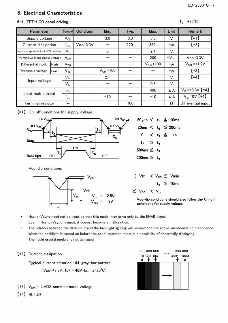
6.Electrical Characteristics
6-1.TFT-LCD panel driving Ta=+25℃
Symbol Unit
VCC V
ICC mA
VL V
VRP mVP-P
High VTH mV
Low VTL mV
VIH V
VIL V
IOH μA
IOL μA
RT Ω
【*1】 On-off conditions for supply voltage
Differential input
Remark
【*1】
【*2】
Vcc=3.3V
VCM -100
- -
Vcc=3.3V -
3.3
-
VI2 =0V 【*4】
VI2 =+3.3V 【*4】
-
VCM =+1.2V
【*3】
【*4】-
VCM +100
Max.
- 2.4
- - 200
3.6
270 350
Supply voltage 3.0
Condition Typ.
-
-
2.1
-10
-
100 -
+10
- 0.8
400
-
-
Parameter
Current dissipation
Input voltage width for LVDS receiver
Permissive input ripple voltage
-
Min.
0
Differential input
Threshold voltage
Input reak current
Terminal resistor
Input voltage
VCCt2
t1 t3
t4
t5 t6
ON
Data
0.9 VCC
0.1 VCC
0.9 VCC
0.1 VCC
20μs < t1 ≦ 10ms
20ms < t2 ≦ 200ms
0 < t3 ≦ 1s
1s ≦ t4
500ms ≦ t5
Vcc-dip conditions
・ Hsync/Vsync need not be input so that this model may drive only by the ENAB signal.
Even if Hsync/Vsync is input, it doesn't become a malfunction.
・ The relation between the data input and the backlight lighting will recommend the above-mentioned input sequence.
When the backlight is turned on before the panel operates, there is a possibility of abnormally displaying.
The liquid crystal module is not damaged.
【*2】 Current dissipation
Typical current situation : 64-gray-bar pattern
【*3】 VCM : LVDS common mode voltage
( Vcc=+3.3V、fck = 40MHz、Ta=25℃)
RGB RGB RGB RGBRGB
GS0 GS1 GS2 GS62 GS63・・・
VCCt2
t1 t3
t4
Back lightt5 t6
ON
OFF OFF
Data
0.9 VCC
0.1 VCC
0.9 VCC
0.1 VCC
Vth
td
VCC
Vmin
Vth = 2.5V
Vmin = 3V
20μs < t1 ≦ 10ms
20ms < t2 ≦ 200ms
0 < t3 ≦ 1s
1s ≦ t4
500ms ≦ t5
200ms ≦ t6
1) Vth < VCC ≦ Vmin
td ≦ 10ms
2) VCC < Vth
Vcc-dip conditions should also follow the On-offconditions for supply voltage
【*4】 RL/UD
RGB RGB RGB RGBRGB
GS0 GS1 GS2 GS62 GS63・・・
VCCt2
t1 t3
t4
Back lightt5 t6
ON
OFF OFF
Data
0.9 VCC
0.1 VCC
0.9 VCC
0.1 VCC
Vth
td
VCC
Vmin
Vth = 2.5V
Vmin = 3V
20μs < t1 ≦ 10ms
20ms < t2 ≦ 200ms
0 < t3 ≦ 1s
1s ≦ t4
500ms ≦ t5
200ms ≦ t6
1) Vth < VCC ≦ Vmin
td ≦ 10ms
2) VCC < Vth
Vcc-dip conditions should also follow the On-offconditions for supply voltage

LD-23301C- 8
6-2.LED backlight
Ta=+25℃
Unit
V
mA
μA
mVP-P
V
V
V
V
Hz
%
ms
ms
0.8
-
- -
L(50,000)
VIL_BL2
HPWM 0.1
(Module)
【*4】
【*4,5】
【*3】
【*4】
【*5】
【*4,5】
fPWM 200 - 1K
-
VDD
VIH_BL1 2.4 -
VIL_BL1
-VIH_BL2
-
2.1
VDD 10.2 12.0
Symbol Min. Typ.
- 0.2
- -
RemarkMax.
13.8 【*1】
【*3】
【*2】500
VDD
IDD1 - 350
VDD=+12.0V
10
200
- -
VRP_BL
IDD2
LPWM - - 4.5 【*5,7】
Life time h【Reference】
【*6】- -
PWM
Frequency
Duty
Pulse width (Lo)
DPWM 10 - 100
Pulse width (Hi)
Supply voltage
Current dissipation
Permissive input ripple voltage
Parameter
VBR
XSTABY High voltage
Low voltage
High voltage
Low voltage
△2
△2
【*1】 On-off conditions for supply voltage
20μs ≦ t7≦ 200ms
0ms ≦ t8≦
0ms ≦ t9≦
200ms ≦ t10≦
0ms ≦ t11≦
0ms ≦ t12≦
【*2】 Current dissipation
Typ. value: VDD=+12.0V、Duty=100%
Max. value: VDD=+10.2V、Duty=100%
【*3】 Backlight ON/OFF signal (connected by the pull-down resistor of 10kΩ)
【*4】 PWM signal (connected by the pull-down resistor of 10kΩ)
VDD t8t7 t9
t10
0.9 VDD
0.1 VDD
0.9 VDD
0.1 VDD
Back light
(LED)
t11 t12
ON
OFF OFF
XSTABY
VBR
PWM
△2
△2
△2
△2
VDD t8t7 t9
t10
0.9 VDD
0.1 VDD
0.9 VDD
0.1 VDD
Back light
(LED)
t11 t12
ON
OFF OFF
XSTABY
VBR
PWM
△2
△2
△2
△2

LD-23301C- 9
【*5】 PWM
fPWM = 1/t14 DPWM = t13 / t14
Duty 10% : Min. Luminance(0%:LED OFF)
Duty 100% : Max. Luminance
Luminance changes in proportion to the duty ratio. (t13≧10μs)
When the frequency slows, the display fineness might decrease.
【*6】 Luminance becomes 50% of an initial value. (Ta=25℃, PWM=100%)
【*7】 When VBR signal is set “Low” more than 4.5ms, please turn off XSTABY.
VBR
t13
t14
t15
△2
VBR
t13
t14
t15
△2

LD-23301C- 10
7.Timing characteristics of input signals
7-1.Timing characteristics
【*1】 In case of using the long vertical period, the deterioration of display quality, flicker etc. may occur.
【*1】
26.4 μs
800 800 800 clock
39.9
remark
35
1395 clock
max unit
42 MHz
typ
1056
40Frequency
23.5
628
1/Tc
ENAB
Horizontal period TH
Horizontal period (High) THd
Vertical Frequency TV
Parameter Symbol
940
min
-
600
ms
line
16.7 -
600 600Vertical period (High) TVd
Clock
line666 798
ENAB
THd
ENAB
DATA
(R,G,B)
ENAB
THd
TVd
TV
1 2
1 2
800
599 600

LD-23301C- 11
7-2.Input Data Signals and Display Position on the screen
D(1,1) D(2,1) D(3,1) D( 800 ,1)
D(1,2) D(2,2)
D(1,3)
D(1, 600 ) D( 800 , 600 )
G BR G B R
( 1, 1 ) ( 2, 1 )
R G B
( 1, 1 ) ( 2, 1 )
R G B
( 1, 1 ) ( 2, 1 )
R G B
LD-23301C- 12
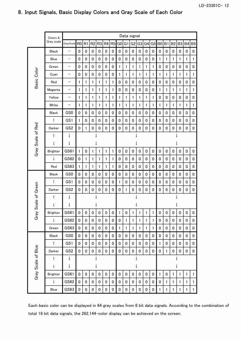
8.Input Signals, Basic Display Colors and Gray Scale of Each Color
R0 R1 R2 R3 R4 R5 G0 G1 G2 G3 G4 G5 B0 B1 B2 B3 B4 B5
Black 0 0 0 0 0 0 0 0 0 0 0 0 0 0 0 0 0 0
Blue 0 0 0 0 0 0 0 0 0 0 0 0 1 1 1 1 1 1
Green 0 0 0 0 0 0 1 1 1 1 1 1 0 0 0 0 0 0
Cyan 0 0 0 0 0 0 1 1 1 1 1 1 1 1 1 1 1 1
Red 1 1 1 1 1 1 0 0 0 0 0 0 0 0 0 0 0 0
Magenta 1 1 1 1 1 1 0 0 0 0 0 0 1 1 1 1 1 1
Yellow 1 1 1 1 1 1 1 1 1 1 1 1 0 0 0 0 0 0
White 1 1 1 1 1 1 1 1 1 1 1 1 1 1 1 1 1 1
Black 0 0 0 0 0 0 0 0 0 0 0 0 0 0 0 0 0 0
↑ 1 0 0 0 0 0 0 0 0 0 0 0 0 0 0 0 0 0
Darker 0 1 0 0 0 0 0 0 0 0 0 0 0 0 0 0 0 0
↑
↓
Brighter 1 0 1 1 1 1 0 0 0 0 0 0 0 0 0 0 0 0
↓ 0 1 1 1 1 1 0 0 0 0 0 0 0 0 0 0 0 0
Red 1 1 1 1 1 1 0 0 0 0 0 0 0 0 0 0 0 0
Black 0 0 0 0 0 0 0 0 0 0 0 0 0 0 0 0 0 0
↑ 0 0 0 0 0 0 1 0 0 0 0 0 0 0 0 0 0 0
Darker 0 0 0 0 0 0 0 1 0 0 0 0 0 0 0 0 0 0
↑
↓
Brighter 0 0 0 0 0 0 1 0 1 1 1 1 0 0 0 0 0 0
↓ 0 0 0 0 0 0 0 1 1 1 1 1 0 0 0 0 0 0
Green 0 0 0 0 0 0 1 1 1 1 1 1 0 0 0 0 0 0
Black 0 0 0 0 0 0 0 0 0 0 0 0 0 0 0 0 0 0
↑ 0 0 0 0 0 0 0 0 0 0 0 0 1 0 0 0 0 0
Darker 0 0 0 0 0 0 0 0 0 0 0 0 0 1 0 0 0 0
↑
↓
Brighter 0 0 0 0 0 0 0 0 0 0 0 0 1 0 1 1 1 1
↓ 0 0 0 0 0 0 0 0 0 0 0 0 0 1 1 1 1 1
Blue 0 0 0 0 0 0 0 0 0 0 0 0 1 1 1 1 1 1
Each basic color can be displayed in 64 gray scales from 6 bit data signals. According to the combination of
total 18 bit data signals, the 262,144-color display can be achieved on the screen.
↓
↓ ↓ ↓
↓ ↓
↓ ↓ ↓
↓ ↓
Bas
ic C
olo
rG
ray
Scal
e o
f R
ed
Gra
y Scal
e o
f G
reen
Gra
y Scal
e o
f B
lue
-
-
GS0
GS1
GS2
GS1
GS63
GS2
↓
↓
GS61
Colors &Gray scale
Data signal
GrayScale
-
GS61
-
-
-
-
-
↓
↓ ↓ ↓
↓ ↓
GS62
GS62
GS63
↓
↓
GS1
GS63
GS0
GS0
GS2
↓
↓
GS61
GS62
↓

13
9.Optical Characteristics
Ta=+25℃, Vcc=+3.3V
Condition Unit
Deg.
Deg.
Deg.
optimizedangle
ms
θ11
Parameter
Viewinganglerange
Symbol Min.
-
CRContrast ratio
θ12
θ=0°
White Black
Chromaticity ofRed
Chromaticity ofGreen
Chromaticity ofBlue
Gy
Gx
Chromaticity ofWhite 0.275
-Response Time
60Vertical
35CR>10
τr +τd
Horizontal θ21,θ22
【*4】
Luminance of white YL1
0.330
0.560Rx
0.3550.305
0.325
【*4】
-
- 0.115
0.595
0.155
0.335
350
By
Ry
0.375
-
-
-
-
Wy
0.255Wx
Bx
-
-
-
-
Typ.
500
60 80
800
80
60
LD-23301C-
【*2,4】
【*3,4】
Max.
-
Remark
-
-
-
【*1,2,4】
-
-
30
- cd/m2450
※The measurement shall be executed 30 minutes after lighting at rating.
The optical characteristics shall be measured in a dark room or equivalent state with the method shown
in Fig.2 below.
Fig.2 Optical characteristics measurement method
White Uniformity -- 1.33 【*5】
Panel center(θ=0°)
Photodetector:(EZ-CONTRAST)
Panel center(θ=0°)
TFT-LCD module
fig.2-1 Measuring method of Viewing angle range.
TFT-LCD module
400mm
Field=1°
fig.2-2 Measuring method of contrast, luminance, response time,
and Chromaticity.
Photodetector
:Response time(BM-5A)
:Contrast/Luminance/Chromaticity(SR-3)

LD-23301C- 14【*1】Definitions of viewing angle range:
【*2】Definition of contrast ratio:
【*3】Definition of response time:
The response time is defined as the following figure and shall be measured by switching the input signal for "black" and "white".
Contrast (CR)=The contrast ratio is defined as the following.Luminance with all pixels white
Luminance with all pixels black
Normal line
θ21θ11
θ12
θ22
6 O'clock
90%100%
White WhiteBlack
tecto
r O
utp
ut
Rela
tive
Val
ue)
【*4】This shall be measured at center of the screen.【*5】Definition of white uniformity:
White uniformity is defined as the following with five measurements.(①~⑤)
200 600 pixel
150
450pixel
400
300
Normal line
θ21θ11
θ12
θ22
6 O'clock
Maximum luminance of 5 points(①~⑤).δw =
Maximum luminance of 5 points(①~⑤).
τd τr
0%10%
90%100%
White WhiteBlack
Time
Photo
dete
cto
r O
utp
ut
(Rela
tive
Val
ue)
1
2 3
45
Normal line
θ21θ11
θ12
θ22
6 O'clock
Maximum luminance of 5 points(①~⑤).δw =
Maximum luminance of 5 points(①~⑤).
τd τr
0%10%
90%100%
White WhiteBlack
Time
Photo
dete
cto
r O
utp
ut
(Rela
tive
Val
ue)
1
2 3
45

LD-23301C- 15
10. Handling Precautions
【Handling Precautions】
a )b )c )
d )e )f )
g )
h )i )j )
k )
l ) m )
【Set-Design Precautions】
a )
b )
c )d )e )
f )
g)
h)
Treat LCD module in dustless surroundings. Metal foreign material stuck to the circuit is possible to cause a short. Be sure to design the cabinet so that the module can be installed without any extra stress such as warp or twist.Be careful not to give any physical stress onto the circuit and/or the connector of LCD module when you pull/plug a cable. Physical stress will cause a break or worse connection.Since the front polarizer is easily damaged, pay attention not to scratch it.Use N2-blower such as an ionized nitrogen has anti-electrostatic when you blow dusts on Polarizer.Since a long contact with water may cause discoloration or spots, wipe it with absorbent cotton or other soft cloth immediately.Since CMOS LSI is used in this module, take care of static electricity and injure the human earth when handling. Observe all other precautionary requirements in handling components.Be careful with the edge parts of the module which is made of metal.Since the panel is made of glass, it may break or crack if dropped or bumped on hard surface. Handle with care.When the panel is broken, don’t touch the glass. Although the panel is difficult to be scattered, touching thebroken part may hurt your hands.Liquid crystal contained in the panel may leak if the LCD is broken. Rinse it as soon as possible if it gets insideyour eye or mouth by mistake.Don’t touch the circuit and the pattern of the board. If you touch it, the circuit may be broken.Follow the regulations when LCD module is scrapped. The government you stay may have some regulations about it.
Notice : Never take to pieces the module , because it will cause failure. Please don't remove the fixed tape, insulating tape etc. that was pasted on the original module. (except for protection film of the panel)Protection film is attached to the module surface to prevent it from being scratched .Peel the film off slowly , just before the use, with strict attention to electrostatic charges. Blow off 'dust' on the polarizer by using an ionized nitrogen.Be sure to design the cabinet so that the module can be installed without any extra stress such as warp or twist.Connect GND to flame of module to stabilize against EMI and external noise.When install LCD modules in the cabinet, please tighten with( “torque=0.294±0.02N・m(3.0±0.2kgf・cm)”).Be sure to confirm it in the same condition as it is installed in your instrument.Since there is a circuit board in the module back, stress is not added at the time of a design assembly. Please make it like. If stress is added, there is a possibility that circuit parts may be damaged.It causes an irregular display and the defective indication, etc., when always put constant pressureon the back of the module. Please do not make the structure to press the back of the module.Be careful of a back light FPC not to pull by force at the time of the connecting to a W-LED driver, or FPC processing.
LD-23301C- 16
i) The polarizer surface on the panel is treated with Anti-Glare for low reflection. In case of attachingsure
j) Don’t change the volume of LCD module. It is optimized when the shipping. Any change may not meet the specification.
k) If a minute particle enters in the module and adheres to an optical material, it may cause display non-uniformity issue, etc. Therefore, fine-pitch filters have to be installed to cooling and inhalation hole if you intend to install a fan.
l) Be sure to follow the absolute maximum rating in the specification. The design should consider the surrounding temperature, the fluctuating input signal, and tolerance of the electronic parts. Exceeding values is possible to cause worse characteristic such as burn and/or broken of the parts on LCD module.
m) Be sure to use LCD module within the recommended operating conditions. Operating module out of the recommended range is not guaranteed even if it is in the absolute maximum rating.
n) Follow the power, signal, and supply voltage sequence which the specification indicates, regarding on-off input signal after power on of LCD module.
o) According to the using application, power circuit protection is recommended at module failure.
【Operation Precautions】
a ) Do not expose the LCD panel to direct sunlight. Lightproof shade etc. should be attached when LCD panel is used under such environment.
b ) When handling LCD modules and assembling them into cabinets, please avoid that long-terms storage in the environment of oxidization or deoxidization gas and the use of such materials as reagent, solvent, adhesive, resin, etc. which generate these gasses, may cause corrosion and discoloration of the modules. Do not use the LCD module under such environment.
c ) An abnormal display by changing in quality of the polarizing plate might occur regardless of contact or no contact to the polarizing plate, because of epoxy resin (amine system curing agent) that comes out from the material and the packaging material used for the set side, the silicon adhesive (dealcoholization system and oxime system),
and the tray blowing agents (azo-compound), etc. Please confirm adaptability with your employed material.d ) Don’t use polychloroprene (CR) with LCD module. It will generate chlorine gas, which will damage the reliability of
the connection part on LCD panel.e ) Be careful when using it for long time with fixed pattern display as it may cause accidential image.
Pleave use a screen saver etc., in order to avoid an afterimage.f ) The LED (Light Emitting Diode) used in this LCD module is very sensitive to temperature change. If it operates
for extremely long time under high temperature, it is possible rapidly to shorten the life time of LED. In case of such a condition, consult with us.
g) If stored at the temperatures lower than the rated storage temperature, the LC may freeze and it may cause LCD panel damage. If storage temperature exceeds the specified rating, the molecular orientation of the LC maychange to that of a liquid, and they may not revert to their original state. Store the module in normal room temperature.
h) Keep LCD module in the range of the specified temperature conditions at all times. Once out of the range, liquid crystal will lose its characteristics, and it cannot recover.
i) Nature of dew consideration prevention is necessary when LCD is used for long time under high-temperatur and high-humidity.
LD-23301C- 17
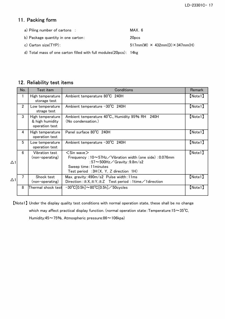
11.Packing form
a) Piling number of cartons : MAX.6
b) Package quantity in one carton: 20pcs
c) Carton size(TYP): 517mm(W) × 432mm(D)×347mm(H)
d) Total mass of one carton filled with full modules(20pcs): 14kg
12.Reliability test items
No.
1
2
3
4
5
△1
6
△17
8
【Note1】 Under the display quality test conditions with normal operation state, these shall be no change
which may affect practical display function. (normal operation state:Temperature:15~35℃,
Humidity:45~75%, Atmospheric pressure:86~106kpa)
Thermal shock test 【Note1】
Vibration test(non-operating)
【Note1】
Shock test(non-operating)
【Note1】
<Sin wave> Frequency :10~57Hz/Vibration width (one side) :0.076mm :57~500Hz/Gravity:9.8m/s2 Sweep time:11minutes Test period :3H(X,Y,Z direction 1H)
Max. gravity:490m/s2 Pulse width:11ms Direction:±X,±Y,±Z Test period :1time/1direction
-30℃[0.5h]~80℃[0.5h]/50cycles
【Note1】
Low temperatureoperation test
【Note1】
High temperatureoperation test
Panel surface 80℃ 240H
Ambient temperature -30℃ 240H
Low temperature strage test
High temperature& high humidityoperation test
Test item
High temperature storage test
Remark
【Note1】
Conditions
Ambient temperature 80℃ 240H
Ambient temperature -30℃ 240H
Ambient temperature 40℃、Humidity 95% RH 240H (No condensation.)
【Note1】
【Note1】
LD-23301C- 18
13.Others13-1.Lot No Label:
A)Module serial label
B)Backlight serial label
The label that displays the model No. and lot No. for the backlight is stuck on the back of the module.
13-2.Packing box Label:
on the packing box. Moreover, the display of bar code also applies to this.
The label that displays SHARP・Model No.( LQ121S1LG84)・Lot No. is stuck on the back of the module.
The label that displays ①Model number( LQ121S1LG84) ②Lot number ③Quantity of module is stuck
Production month (1-9X, Y, Z)
Production year
(Last digit of dominical year)
Lot No display method(Figure and alphabet)
Serial No.
Assembly site code
Discernment code
Model No.
Bar Code(Lot No.)
Lot No.
SHARPLQ121S1LG84
XXXXXXXXXX
Model No.(Figure and alphabet)
Lot No.(Figure and alphabet)
******-**
******-*
( )
① Model number( LQ121S1LG84)
② Lot number (DATA)
③ Quantity of module
A right picture is written to the packing box of module for the RoHS restriction.
※ R.C.(RoHs Compliance)means these parts have corresponded with the RoHs directive.
This module corresponds from the first sample to RoHS Directive.
The figure below is written under the SHARP logo of the packing box about the production country.
13-3. The ozone-depleting substances is not used.
13-4. If any problem occurs in relation to the description of this specification , it shall be resolved through
discussion with spirit of cooperation.
Production month (1-9X, Y, Z)
Production year
(Last digit of dominical year)
Lot No display method(Figure and alphabet)
Serial No.
Assembly site code
Discernment code
R.C.
OR
Model No.
Bar Code(Lot No.)
Lot No.
SHARPLQ121S1LG84
XXXXXXXXXX
Model No.(Figure and alphabet)
Lot No.(Figure and alphabet)
******-**
******-*
社内品番:
Lot No. : (1T) 2011. 03. 05 **
Quantity : (Q) 20 pcs
ユーザー品番 :
シャープ物流用ラベルです。
Our management product number might be filled(Example: LQ121S1LG84A etc.)
Bar code(①)
Bar code(②)
Bar code(③)
(4S) LQ121S1LG84
p p
Production month (1-9X, Y, Z)
Production year
(Last digit of dominical year)
Lot No display method(Figure and alphabet)
Serial No.
Assembly site code
Discernment code
R.C.
OR
Model No.
Bar Code(Lot No.)
Lot No.
SHARPLQ121S1LG84
XXXXXXXXXX
Model No.(Figure and alphabet)
Lot No.(Figure and alphabet)
******-**
******-*
社内品番:
Lot No. : (1T) 2011. 03. 05 **
Quantity : (Q) 20 pcs
ユーザー品番 :
シャープ物流用ラベルです。
Our management product number might be filled(Example: LQ121S1LG84A etc.)
Bar code(①)
Bar code(②)
Bar code(③)
(4S) LQ121S1LG84

LD-23301C- 19
14.Storage conditionsEnvironmental condition range of storage temperature and humidity
Temperature 0 to 40 degrees Celsius
Relative humidity 95% and below
【Note】Please refer below as a mean value of the environmental conditions.
Summer time temperature 20 to 35 degrees Celsius humidity , 85% and below
Winter time temperature 5 to 15 degrees Celsius humidity , 85% and below
Please maintain within 240 hours of accumulated length of storage time, with conditions of 40 degrees
Celsius and room humidity of 95%.
Direct sun light
Please keep the product in a dark room or cover the product to protect from direct sun light.
Atmospheric condition
Please refrain from keeping the product with possible corrosive gas or volatile flux.
Prevention of dew
Please store the product carton either on a wooden pallet or a stand / rack to prevent dew.
Do not place directly on the floor. In addition, to obtain moderate ventilation in between the pallet’s
top and bottom surfaces, pile the cartons up in a single direction and in order.
Please place the product cartons away from the storage wall.
Storage period
Within above mentioned conditions, maximum storage period should be one year.

LD-23301C- 20LD-23301C- 20
Fig .1 : LQ121S1LG84 OUTLINE
LD-23301C- 20

LD-23301C- 21
Fig 3 : PACKING FORM