Embed Size (px)
Citation preview

14. Semiconductor Devices
By Ritesh Hariram
14.1. Introduction to Semiconductor Devices
Semiconductor devices are electronic components that exploit the electronic
properties of semiconductor materials, principally silicon, germanium, and gallium
arsenide, as well as organic semiconductors. Semiconductors are thus materials
whose conductivity lies between a good conductor and a good insulator.
14.1.1. Component Data
A datasheet, data sheet, or spec sheet is a document that summarizes the
performance and other technical characteristics of a product, machine, component
(e.g., an electronic component), material, a subsystem (e.g., a power supply) or
software in sufficient detail to be used by a design engineer to integrate the
component into a system.
14.1.2. Component Data Sources
The following are examples of component data sources
The internet has a wide variety of sources.
Manufacturers make their data sheets public knowledge so getting a hold of
this may be in your best interest.
Most libraries have a Technical section which should have sources in this
regard.
Your local electronics hobby store. These stores have an abundance of data
sheets.
14.1.3. How to read a data sheet?
Consider the diagram below. The diagram shows a typical datasheet for a diode. As
mentioned earlier datasheets can be sourced from a variety websites, textbooks and
electronic stores. This particular datasheet clearly displays the company logo as well
as a picture depicting what the physical component looks like. The datasheet has
been modified to show you exactly where important information can be found.
(Fairchild Semiconductor)


14.1.4. Pin Configuration
In electronics, a pin out (sometimes written "pin-out") is a cross-reference between
the contacts, or pins, of an electrical connector or electronic component, and their
functions
14.1.5. Typical Operating Values
This is a value on the datasheet that describes the typical operating parameters of a
component. It is wise that the user does not exceed these values as it would destroy
the component.
14.1.6. Working Temperature
Electronic components are designed to work within certain temperature parameters.
Working out of these parameters may either damage the component or not produce
the desired result. It is important to consult the manufacturer’s datasheet in this
regard.
14.1.7. Equivalent Components
These are components that perform the same function as the component you are
researching. Often these can be found on certain manufacturer’s datasheets.
14.1.8. Dual in Line Packages
In microelectronics, a dual in-line package (DIP or DIL) is an electronic device
package with a rectangular housing and two parallel rows of electrical connecting
pins. The package may be through-hole mounted to a printed circuit board or
inserted in a socket. Dual-in-line packages were developed in the 1960s when the
restricted number of leads available on transistor-style packages became a limitation
in the use of integrated circuits.
Figure 1: Dual in Line Package
14.1.9. Through Hole Components vs. Surface Mount (SMT)
There are some points that make SMT different from Through Hole, which has been
briefly summarized below:
SMT has helped significantly in solving the space problems that were
commonly noticed with the Through Hole mounting.

The pin count has increased greatly in SMT when compared to its older
counterparts.
In SMT, the components are leadless and are directly mounted to the board
surface. In Through Hole the components have lead wires that are taken to
the wiring boards via holes.
The Pads on the surface in SMT are not used for connection of layers on the
printed wiring boards.
The components in the Though Hole Technology are larger which leads to
lower component density per unit area. The packing density that can be
achieved with SMT is very high as this allows mounting component on both
sides, when needed.
SMT has made possible the applications that seemed impossible with
through-hole components.
SMT is suitable for high volume production that gives access to lowered cost
of unit assemblies which is not possible with through-hole technology.
With SMT acquiring higher circuit speed is easier due to the reduced size.
SMT fulfils one of the prime marketing requirements while assisting in making
high performance circuits in a very small size.
SMT has a disadvantage as the capital investment involved in its machinery
and production is higher.
Designing, production, skill and technology required in implementing SMT is
very advanced when compared to through-hole technology.
Figure 2 through-hole component
Figure 3: Surface mounted components
14.2. Semiconductors
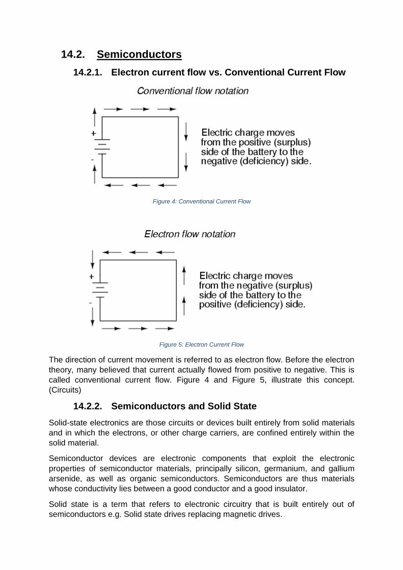
14.2.1. Electron current flow vs. Conventional Current Flow
Figure 4: Conventional Current Flow
Figure 5: Electron Current Flow
The direction of current movement is referred to as electron flow. Before the electron
theory, many believed that current actually flowed from positive to negative. This is
called conventional current flow. Figure 4 and Figure 5, illustrate this concept.
(Circuits)
14.2.2. Semiconductors and Solid State
Solid-state electronics are those circuits or devices built entirely from solid materials
and in which the electrons, or other charge carriers, are confined entirely within the
solid material.
Semiconductor devices are electronic components that exploit the electronic
properties of semiconductor materials, principally silicon, germanium, and gallium
arsenide, as well as organic semiconductors. Semiconductors are thus materials
whose conductivity lies between a good conductor and a good insulator.
Solid state is a term that refers to electronic circuitry that is built entirely out of
semiconductors e.g. Solid state drives replacing magnetic drives.
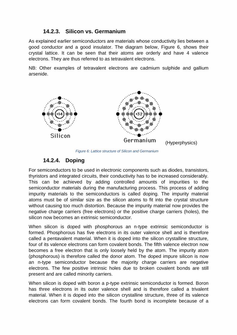
14.2.3. Silicon vs. Germanium
As explained earlier semiconductors are materials whose conductivity lies between a
good conductor and a good insulator. The diagram below, Figure 6, shows their
crystal lattice. It can be seen that their atoms are orderly and have 4 valence
electrons. They are thus referred to as tetravalent electrons.
NB: Other examples of tetravalent electrons are cadmium sulphide and gallium
arsenide.
(Hyperphysics)
Figure 6: Lattice structure of Silicon and Germanium
14.2.4. Doping
For semiconductors to be used in electronic components such as diodes, transistors,
thyristors and integrated circuits, their conductivity has to be increased considerably.
This can be achieved by adding controlled amounts of impurities to the
semiconductor materials during the manufacturing process. This process of adding
impurity materials to the semiconductors is called doping. The impurity material
atoms must be of similar size as the silicon atoms to fit into the crystal structure
without causing too much distortion. Because the impurity material now provides the
negative charge carriers (free electrons) or the positive charge carriers (holes), the
silicon now becomes an extrinsic semiconductor.
When silicon is doped with phosphorous an n-type extrinsic semiconductor is
formed. Phosphorous has five electrons in its outer valence shell and is therefore
called a pentavalent material. When it is doped into the silicon crystalline structure,
four of its valence electrons can form covalent bonds. The fifth valence electron now
becomes a free electron that is only loosely held by the atom. The impurity atom
(phosphorous) is therefore called the donor atom. The doped impure silicon is now
an n-type semiconductor because the majority charge carriers are negative
electrons. The few positive intrinsic holes due to broken covalent bonds are still
present and are called minority carriers.
When silicon is doped with boron a p-type extrinsic semiconductor is formed. Boron
has three electrons in its outer valence shell and is therefore called a trivalent
material. When it is doped into the silicon crystalline structure, three of its valence
electrons can form covalent bonds. The fourth bond is incomplete because of a
missing electron. The hole that exists because of the missing electron acts like a
positive charge that can attract an electron from any nearby silicon atom. The
impurity atom (boron) is therefore called the acceptor atom. The doped impure
silicon is now a p-type semiconductor because the majority charge carriers are
positive holes. The few negative intrinsic electrons due to broken covalent bonds are
still present and are called minority carriers. (swart, pp. 184-188)
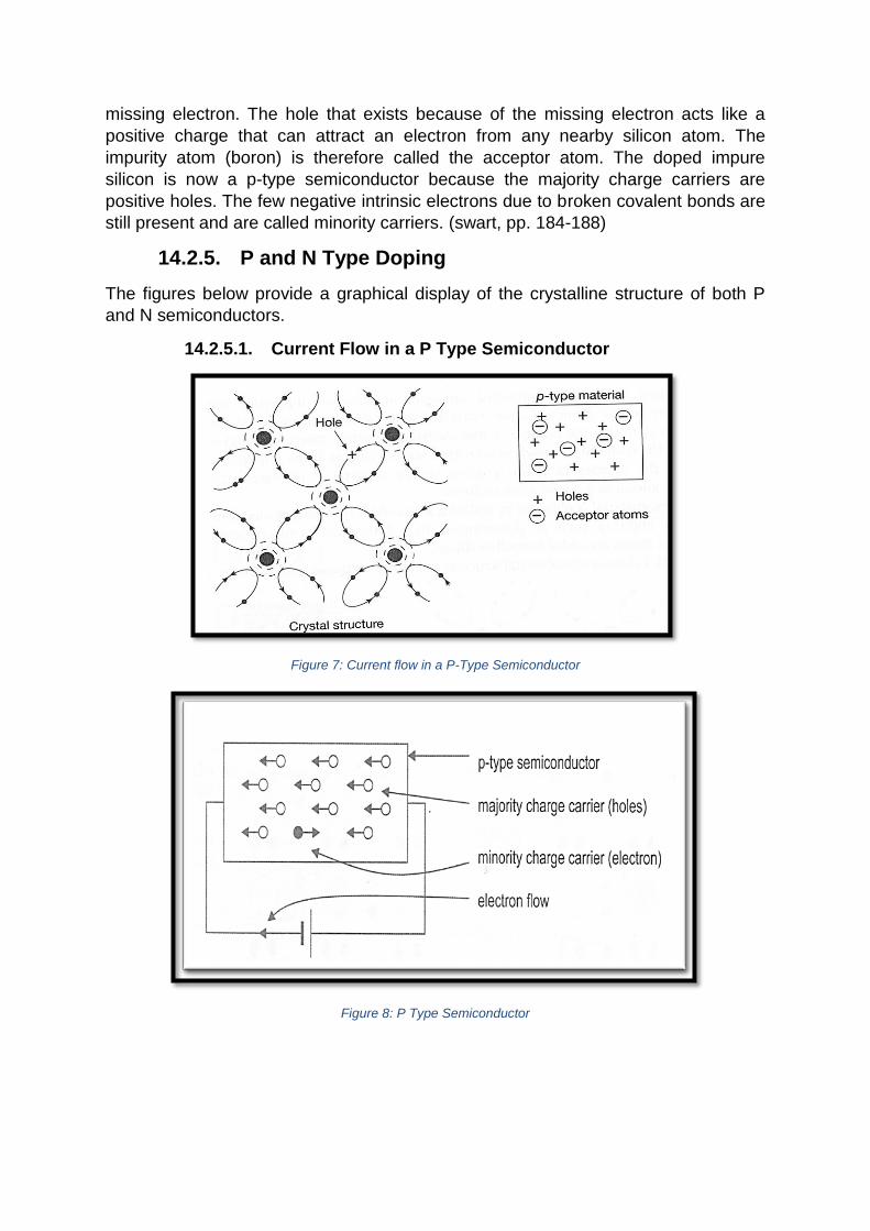
14.2.5. P and N Type Doping
The figures below provide a graphical display of the crystalline structure of both P
and N semiconductors.
14.2.5.1. Current Flow in a P Type Semiconductor
Figure 7: Current flow in a P-Type Semiconductor
Figure 8: P Type Semiconductor
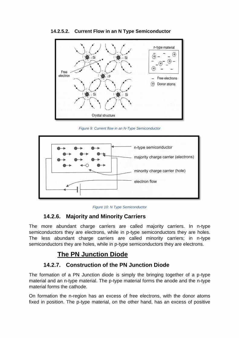
14.2.5.2. Current Flow in an N Type Semiconductor
Figure 9: Current flow in an N-Type Semiconductor
Figure 10: N Type Semiconductor
14.2.6. Majority and Minority Carriers
The more abundant charge carriers are called majority carriers. In n-type
semiconductors they are electrons, while in p-type semiconductors they are holes.
The less abundant charge carriers are called minority carriers; in n-type
semiconductors they are holes, while in p-type semiconductors they are electrons.
The PN Junction Diode
14.2.7. Construction of the PN Junction Diode
The formation of a PN Junction diode is simply the bringing together of a p-type
material and an n-type material. The p-type material forms the anode and the n-type
material forms the cathode.
On formation the n-region has an excess of free electrons, with the donor atoms
fixed in position. The p-type material, on the other hand, has an excess of positive

holes, with the acceptor atoms fixed in position. Because of thermal agitation the n-
region will also contain a few positive holes and the p-region a few free electrons.
When the junction is formed, the free electrons in the n-region tend to diffuse into the
p-region. Similarly, holes tend to diffuse into the n-region. The result of this diffusion
is that the n-region assumes a net positive charge and the p-region a net negative
charge.
Because of this charge distribution a potential difference exists across the junction.
This internal potential barrier tends to oppose the further flow of electrons and holes
and may be represented by a virtual battery across the junction. Electrons diffusing
across the junction recombine with existing free electrons, with the result that the
region in the vicinity of the junction becomes devoid of charge carriers. This is known
as the depletion region.
Figure 11, below shows the circuit symbol and block diagram of the PN Junction
Diode. (swart, pp. 186-193)
Figure 11: Circuit symbol and block diagram of PN Junction diode
14.2.8. The Depletion Region
In semiconductor physics, the depletion region, also called depletion layer, depletion
zone, junction region, space charge region or space charge layer, is an insulating
region within a conductive, doped semiconductor material where the mobile charge
carriers have diffused away, or have been forced away by an electric field. The only
elements left in the depletion region are ionized donor or acceptor impurities.
(Wikipedia)
14.2.9. Forward and Reverse Biasing
14.2.9.1. Forward Biasing
When an external battery is connected with its positive terminal to the p-type material
and its negative terminal to the n-type material, the junction is said to be forward
biased. The threshold of voltage across the diode is about 0.6 V for silicon and about
0.2 V for germanium.
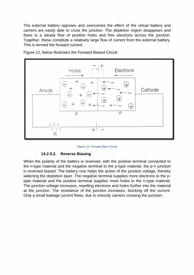
The external battery opposes and overcomes the effect of the virtual battery and
carriers are easily able to cross the junction. The depletion region disappears and
there is a steady flow of positive holes and free electrons across the junction.
Together, these constitute a relatively large flow of current from the external battery.
This is termed the forward current.
Figure 12, below illustrates the Forward Biased Circuit
Figure 12: Forward Bias Circuit
14.2.9.2. Reverse Biasing
When the polarity of the battery is reversed, with the positive terminal connected to
the n-type material and the negative terminal to the p-type material, the p-n junction
is reversed biased. The battery now helps the action of the junction voltage, thereby
widening the depletion layer. The negative terminal supplies more electrons to the p-
type material and the positive terminal supplies more holes to the n-type material.
The junction voltage increases, repelling electrons and holes further into the material
at the junction. The resistance of the junction increases, blocking off the current.
Only a small leakage current flows, due to minority carriers crossing the junction.

Figure 13: Reverse Bias Circuit (Swart)
14.2.10. Characteristic Curve and Symbol
Figure 14: Characteristic curve of a diode
When connected in reverse bias (negative to the anode and positive to the cathode),
the depletion region will increase. Only a small leakage current will flow. If the
reverse voltage increases, the depletion region will increase as well. If this voltage
increases continuously, a point will be met when the depletion region takes over the
entire pn-junction and the diode will break down.
When forward biased (positive on the anode and negative on the cathode), then the
depletion region will decrease. If the forward bias voltage is reached (0.6 V for silicon
and 0.3 V for germanium), then conduction will take place. The amount of current
that flows will be directly proportional to the amount of applied voltage (ohm’s law).
14.2.11. The Diode Load Line
A load line is used in graphical analysis of nonlinear electronic circuits; representing
the constraint other parts of the circuit place on a non-linear device, like a diode or
transistor. It is usually drawn on a graph of the current vs the voltage in the nonlinear
device, called the device's characteristic curve. A load line, usually a straight line,

represents the response of the linear part of the circuit, connected to the nonlinear
device in question. The operating point(s) of the circuit are the points where the
characteristic curve and the load line intersect; at these points the current and
voltage parameters of both parts of the circuit match. (Ref Wikipedia)
From the characteristic curve of the diode we see that this curve is not linear. It is
therefore not easy to calculate at which point the diode is operating at, because we
don’t have a formula for the curve. However, we can determine the operating point
graphically. If the diode is connected to a DC energy source in series with a load
resistor we can find a point on the curve at which the diode is operating. To find this
out we need to plot the characteristic curve of the resistor on that same characteristic
curve of the diode. The intersection of these two graphs thus results in the Q-Point
which is the operating point of the diode.
At the Q-Point 𝐈𝐝 = 𝐈𝐫
𝐕𝐒=𝐕𝐝 + 𝐕𝐫
= 𝐕𝐝 + 𝐈𝐫 × 𝐑𝐥𝐨𝐚𝐝
Where:
𝐕𝐒 = 𝐒𝐮𝐩𝐩𝐥𝐲 𝐕𝐨𝐥𝐭𝐚𝐠𝐞
𝐕𝐝 = 𝐃𝐢𝐨𝐝𝐞 𝐕𝐨𝐥𝐭𝐚𝐠𝐞
𝐕𝐫 = 𝐑𝐞𝐬𝐢𝐬𝐭𝐨𝐫 𝐕𝐨𝐥𝐭𝐚𝐠𝐞
𝐈𝐝 = 𝐃𝐢𝐨𝐝𝐞 𝐂𝐮𝐫𝐫𝐞𝐧𝐭
𝐈𝐫 = 𝐑𝐞𝐬𝐢𝐬𝐭𝐨𝐫 𝐂𝐮𝐫𝐫𝐞𝐧𝐭
(swart)
Figure 15: Diode DC Load line superimposed onto Diode Characteristic Curve
Example 1
A silicon PN junction diode is connected to a 10V supply in series with a 1.25kΩ load
resistor. Use a dc load line to determine the Q-point at which the diode is operating.
Solution
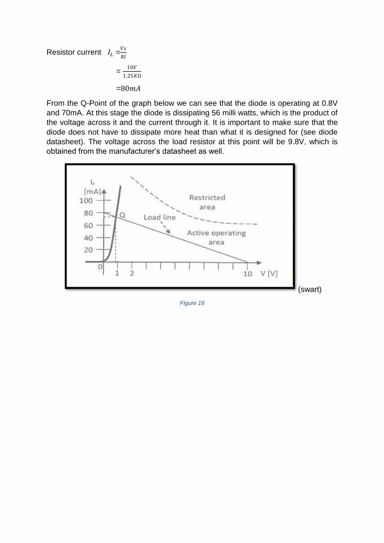
Resistor current 𝐼𝐿 =𝑉𝑠
𝑅𝑙
= 10𝑉
1.25𝐾Ω
=80𝑚𝐴
From the Q-Point of the graph below we can see that the diode is operating at 0.8V
and 70mA. At this stage the diode is dissipating 56 milli watts, which is the product of
the voltage across it and the current through it. It is important to make sure that the
diode does not have to dissipate more heat than what it is designed for (see diode
datasheet). The voltage across the load resistor at this point will be 9.8V, which is
obtained from the manufacturer’s datasheet as well.
(swart)
Figure 16
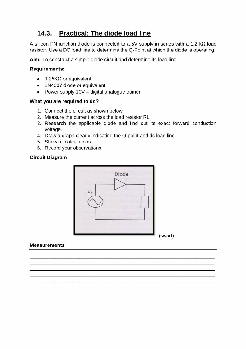
14.3. Practical: The diode load line
A silicon PN junction diode is connected to a 5V supply in series with a 1.2 kΩ load
resistor. Use a DC load line to determine the Q-Point at which the diode is operating.
Aim: To construct a simple diode circuit and determine its load line.
Requirements:
1.25KΩ or equivalent
1N4007 diode or equivalent
Power supply 10V – digital analogue trainer
What you are required to do?
1. Connect the circuit as shown below.
2. Measure the current across the load resistor RL
3. Research the applicable diode and find out its exact forward conduction
voltage.
4. Draw a graph clearly indicating the Q-point and dc load line
5. Show all calculations.
6. Record your observations.
Circuit Diagram
(swart)
Measurements
___________________________________________________________________
___________________________________________________________________
___________________________________________________________________
___________________________________________________________________
___________________________________________________________________
Redraw Circuit diagram with measurements
Graph
Calculations
___________________________________________________________________
___________________________________________________________________
___________________________________________________________________
___________________________________________________________________
___________________________________________________________________
Observations
___________________________________________________________________
___________________________________________________________________
___________________________________________________________________
___________________________________________________________________
14.4. The Zener Diode
14.4.1. Construction
A Zener diode is a silicon junction diode that is designed for voltage stabilization,
since it has the ability to maintain a constant voltage across its terminals under
reverse bias conditions. When it is forward biased, it behaves like an ordinary
junction diode. It is constructed in the same way as a PN Junction diode, but the
doping levels are much higher, in order to lower the reverse breakdown levels to a
few volts. Zener diodes with reverse breakdown voltages of between 3 V and 30 V
are available.
14.4.2. Principle of operation
A conventional solid-state diode allows significant current if it is reverse-biased
above its reverse breakdown voltage. When the reverse bias breakdown voltage is
exceeded, a conventional diode is subject to high current due to avalanche
breakdown. Unless this current is limited by circuitry, the diode may be permanently
damaged or destroyed due to overheating. A Zener diode exhibits almost the same
properties, except the device is specially designed so as to have a reduced
breakdown voltage, the so-called Zener voltage. By contrast with the conventional
device, a reverse-biased Zener diode exhibits a controlled breakdown and allows the
current to keep the voltage across the Zener diode close to the Zener breakdown
voltage. For example, a diode with a Zener breakdown voltage of 3.2 V exhibits a
voltage drop of very nearly 3.2 V across a wide range of reverse currents. The Zener
diode is therefore ideal for applications such as the generation of a reference voltage
(e.g. for an amplifier stage), or as a voltage stabilizer for low-current applications.
14.4.3. Forward Biasing
When forward-biased, zener diodes behave much the same as standard rectifying
diodes: they have a forward voltage drop which follows the “diode equation” and is
about 0.7 volts for silicon and 0.3 V for germanium.
14.4.4. Reverse Biasing
In reverse-bias mode, they do not conduct until the applied voltage reaches or
exceeds the so-called zener voltage, at which point the diode is able to conduct
substantial current, and in doing so will try to limit the voltage dropped across it to
that zener voltage point. So long as the power dissipated by this reverse current
does not exceed the diode's thermal limits, the diode will not be harmed.
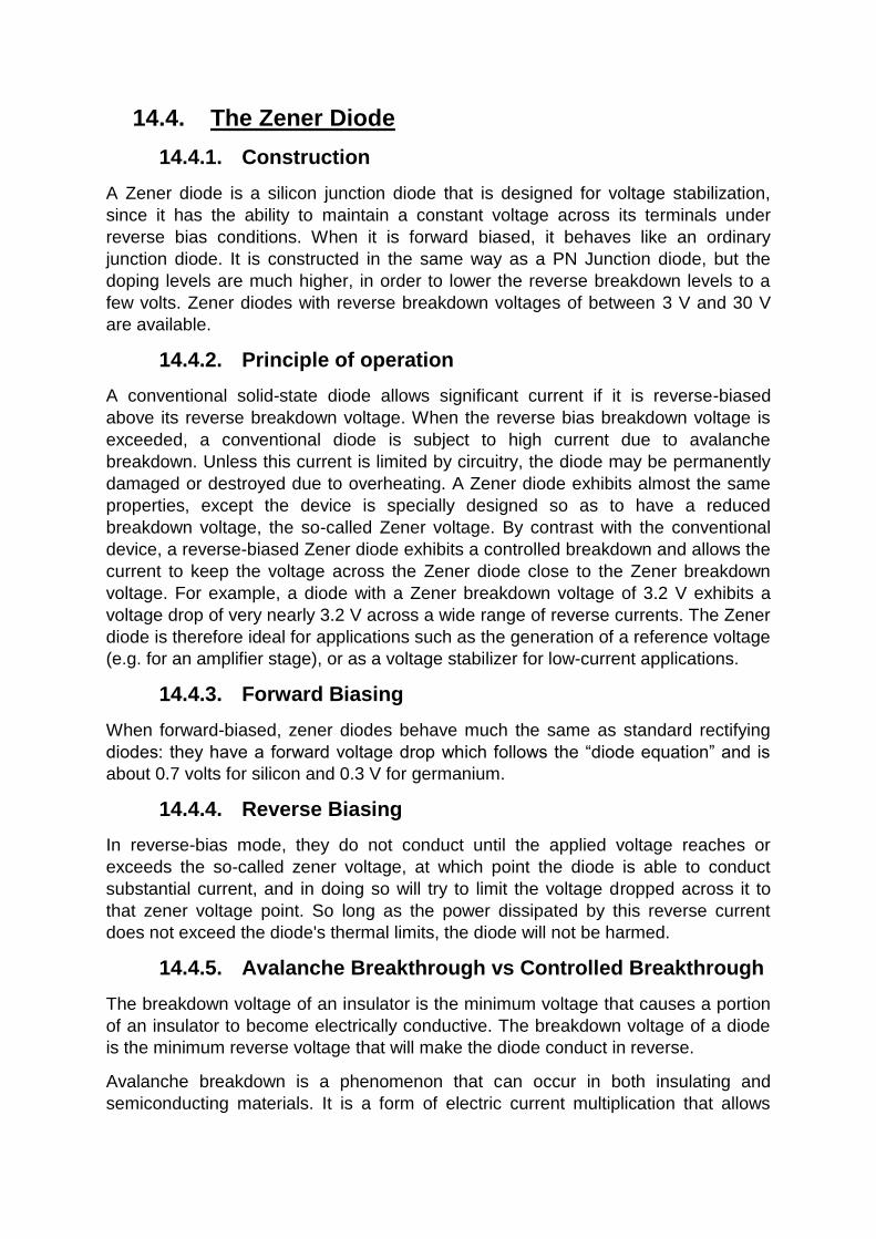
14.4.5. Avalanche Breakthrough vs Controlled Breakthrough
The breakdown voltage of an insulator is the minimum voltage that causes a portion
of an insulator to become electrically conductive. The breakdown voltage of a diode
is the minimum reverse voltage that will make the diode conduct in reverse.
Avalanche breakdown is a phenomenon that can occur in both insulating and
semiconducting materials. It is a form of electric current multiplication that allows
very large currents within materials which are otherwise good insulators. It is a type
of electron avalanche. The avalanche process occurs when the carriers in the
transition region are accelerated by the electric field and energies sufficiently to free
electron-hole pairs via collisions with bound electrons.
The Zener effect is a type of electrical breakdown in a reverse biased p-n diode in
which the electric field enables tunnelling of electrons from the valence to the
conduction band of a semiconductor, leading to a large number of free minority
carriers, which suddenly increase the reverse current. Zener breakdown is employed
in a Zener diode.
Either the Zener or the avalanche effect may occur independently, or both may occur
simultaneously. In general, diode junctions which break down below 5 V are caused
by the Zener effect, while junctions which experience breakdown above 5 V are
caused by the avalanche effect. Figure 17 below demonstrates graphically the
relationship between Avalanche Breakthrough and Controlled breakthrough.
(Hyperphysics)
Figure 17: Relationship between Avalanche Breakthrough and Controlled Breakthrough
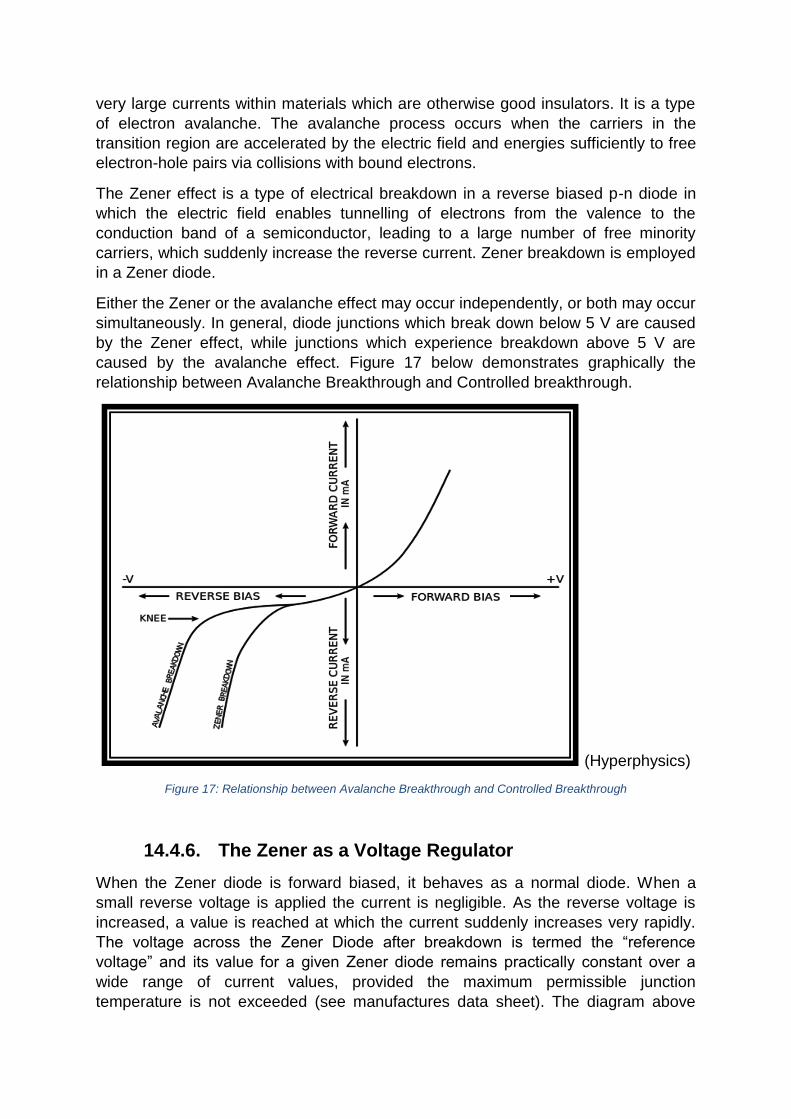
14.4.6. The Zener as a Voltage Regulator
When the Zener diode is forward biased, it behaves as a normal diode. When a
small reverse voltage is applied the current is negligible. As the reverse voltage is
increased, a value is reached at which the current suddenly increases very rapidly.
The voltage across the Zener Diode after breakdown is termed the “reference
voltage” and its value for a given Zener diode remains practically constant over a
wide range of current values, provided the maximum permissible junction
temperature is not exceeded (see manufactures data sheet). The diagram above
shows how a Zener Diode can be used as a voltage stabiliser. The purpose of the
series resistor is to limit the reverse current through the diode to a safe value.
Figure 18: Zener Voltage Stabiliser
14.4.7. The Zener Characteristic Curve and Symbol
Figure 19: The Zener Symbol
(Talkingelectronics.com)
Figure 20: Zener Diode Characteristic Curve
R1 1
kZ
1 1
N2804
+
-
+
-
Variable Voltage
Constant Voltage
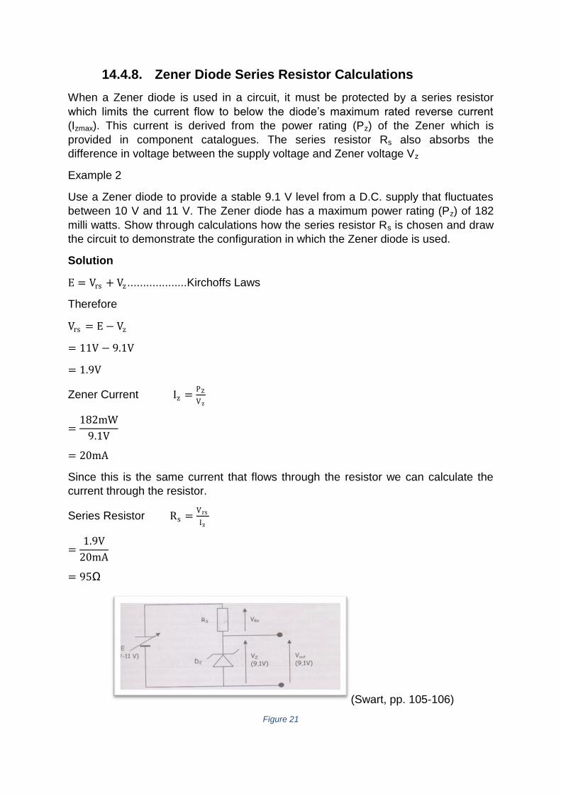
14.4.8. Zener Diode Series Resistor Calculations
When a Zener diode is used in a circuit, it must be protected by a series resistor
which limits the current flow to below the diode’s maximum rated reverse current
(Izmax). This current is derived from the power rating (Pz) of the Zener which is
provided in component catalogues. The series resistor Rs also absorbs the
difference in voltage between the supply voltage and Zener voltage Vz
Example 2
Use a Zener diode to provide a stable 9.1 V level from a D.C. supply that fluctuates
between 10 V and 11 V. The Zener diode has a maximum power rating (Pz) of 182
milli watts. Show through calculations how the series resistor Rs is chosen and draw
the circuit to demonstrate the configuration in which the Zener diode is used.
Solution
E = Vrs + Vz ...................Kirchoffs Laws
Therefore
Vrs = E − Vz
= 11V − 9.1V
= 1.9V
Zener Current Iz =PZ
Vz
=182mW
9.1V
= 20mA
Since this is the same current that flows through the resistor we can calculate the
current through the resistor.
Series Resistor Rs =Vrs
Iz
=1.9V
20mA
= 95Ω
(Swart, pp. 105-106)
Figure 21
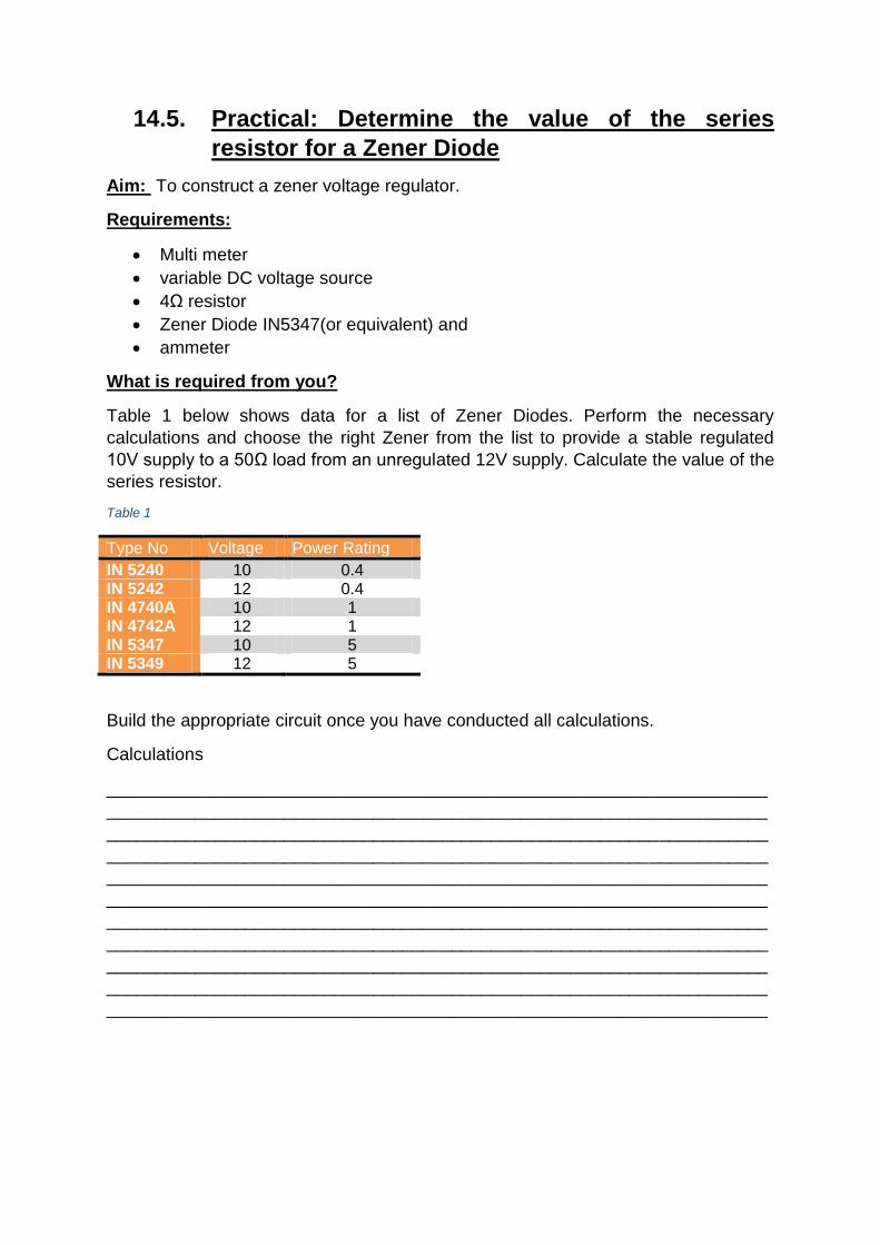
14.5. Practical: Determine the value of the series
resistor for a Zener Diode
Aim: To construct a zener voltage regulator.
Requirements:
Multi meter
variable DC voltage source
4Ω resistor
Zener Diode IN5347(or equivalent) and
ammeter
What is required from you?
Table 1 below shows data for a list of Zener Diodes. Perform the necessary
calculations and choose the right Zener from the list to provide a stable regulated
10V supply to a 50Ω load from an unregulated 12V supply. Calculate the value of the
series resistor.
Table 1
Type No Voltage Power Rating
IN 5240 10 0.4 IN 5242 12 0.4 IN 4740A 10 1 IN 4742A 12 1 IN 5347 10 5 IN 5349 12 5
Build the appropriate circuit once you have conducted all calculations.
Calculations
___________________________________________________________________
___________________________________________________________________
___________________________________________________________________
___________________________________________________________________
___________________________________________________________________
___________________________________________________________________
___________________________________________________________________
___________________________________________________________________
___________________________________________________________________
___________________________________________________________________
___________________________________________________________________

Draw the circuit diagram
Build your circuit and let your teacher check it before you turn on the power.
14.6. The NPN Transistor
The transistor is a 3 element device made up of semiconductor materials. One of the
popular methods of manufacturing a transistor is by growing a crystal. Transistors
are made, and the junctions between elements are formed, by methods similar to
those used to make a PN Junction Diode.
Transistors are used to control current (switch) or to amplify an input voltage or
current. They are used to amplify an extremely small radio signal to a much larger
signal, strong enough to operate the radio’s loudspeaker. Transistors are also used
as electronic switches in logic and computer circuits.
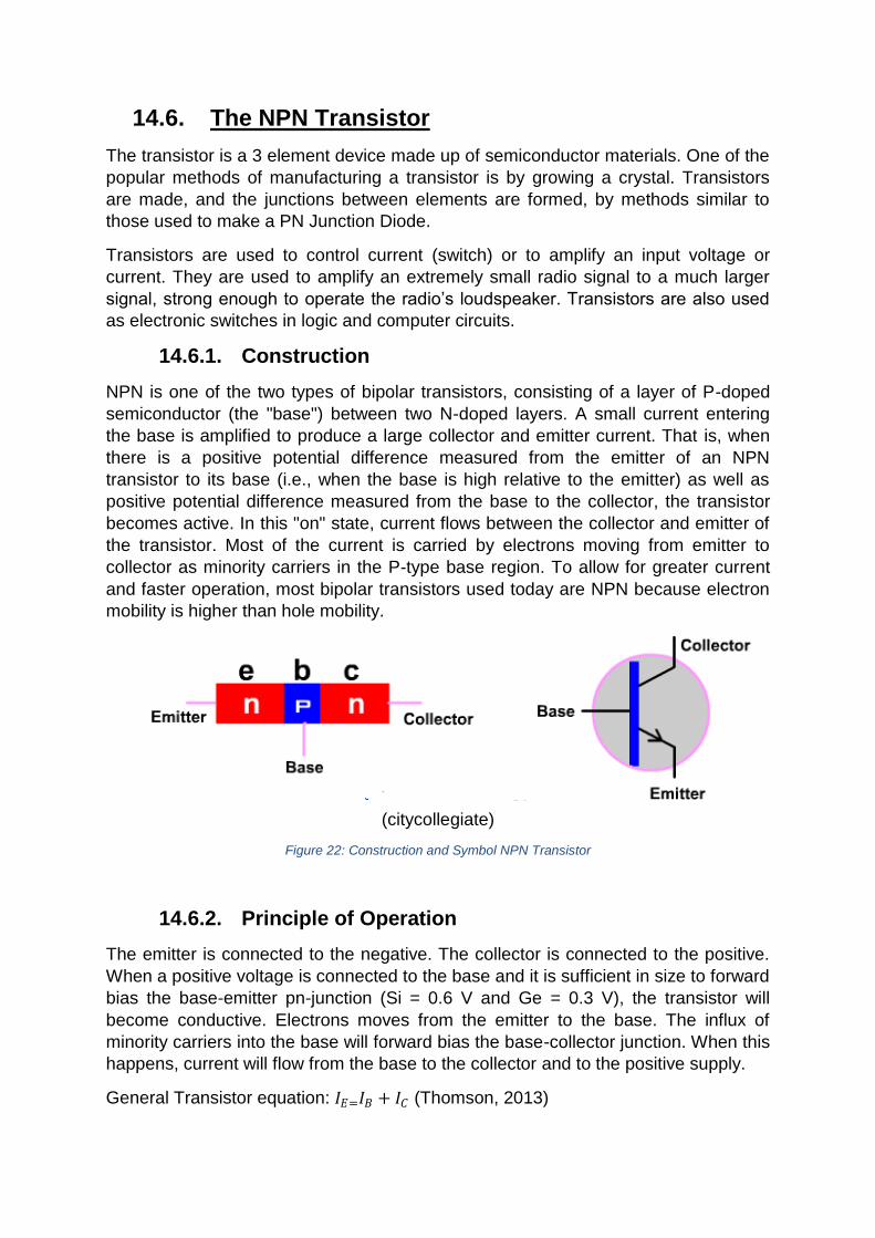
14.6.1. Construction
NPN is one of the two types of bipolar transistors, consisting of a layer of P-doped
semiconductor (the "base") between two N-doped layers. A small current entering
the base is amplified to produce a large collector and emitter current. That is, when
there is a positive potential difference measured from the emitter of an NPN
transistor to its base (i.e., when the base is high relative to the emitter) as well as
positive potential difference measured from the base to the collector, the transistor
becomes active. In this "on" state, current flows between the collector and emitter of
the transistor. Most of the current is carried by electrons moving from emitter to
collector as minority carriers in the P-type base region. To allow for greater current
and faster operation, most bipolar transistors used today are NPN because electron
mobility is higher than hole mobility.
(citycollegiate)
Figure 22: Construction and Symbol NPN Transistor
14.6.2. Principle of Operation
The emitter is connected to the negative. The collector is connected to the positive.
When a positive voltage is connected to the base and it is sufficient in size to forward
bias the base-emitter pn-junction (Si = 0.6 V and Ge = 0.3 V), the transistor will
become conductive. Electrons moves from the emitter to the base. The influx of
minority carriers into the base will forward bias the base-collector junction. When this
happens, current will flow from the base to the collector and to the positive supply.
General Transistor equation: 𝐼𝐸=𝐼𝐵 + 𝐼𝐶 (Thomson, 2013)
14.6.3. The Purpose of Biasing and Thermal Runaway
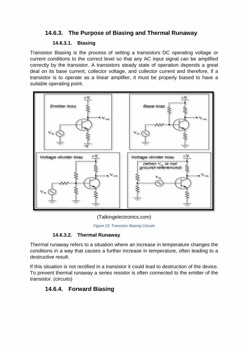
14.6.3.1. Biasing
Transistor Biasing is the process of setting a transistors DC operating voltage or
current conditions to the correct level so that any AC input signal can be amplified
correctly by the transistor. A transistors steady state of operation depends a great
deal on its base current, collector voltage, and collector current and therefore, if a
transistor is to operate as a linear amplifier, it must be properly biased to have a
suitable operating point.
(Talkingelectronics.com)
Figure 23: Transistor Biasing Circuits
14.6.3.2. Thermal Runaway
Thermal runaway refers to a situation where an increase in temperature changes the
conditions in a way that causes a further increase in temperature, often leading to a
destructive result.
If this situation is not rectified in a transistor it could lead to destruction of the device.
To prevent thermal runaway a series resistor is often connected to the emitter of the
transistor. (circuits)
14.6.4. Forward Biasing
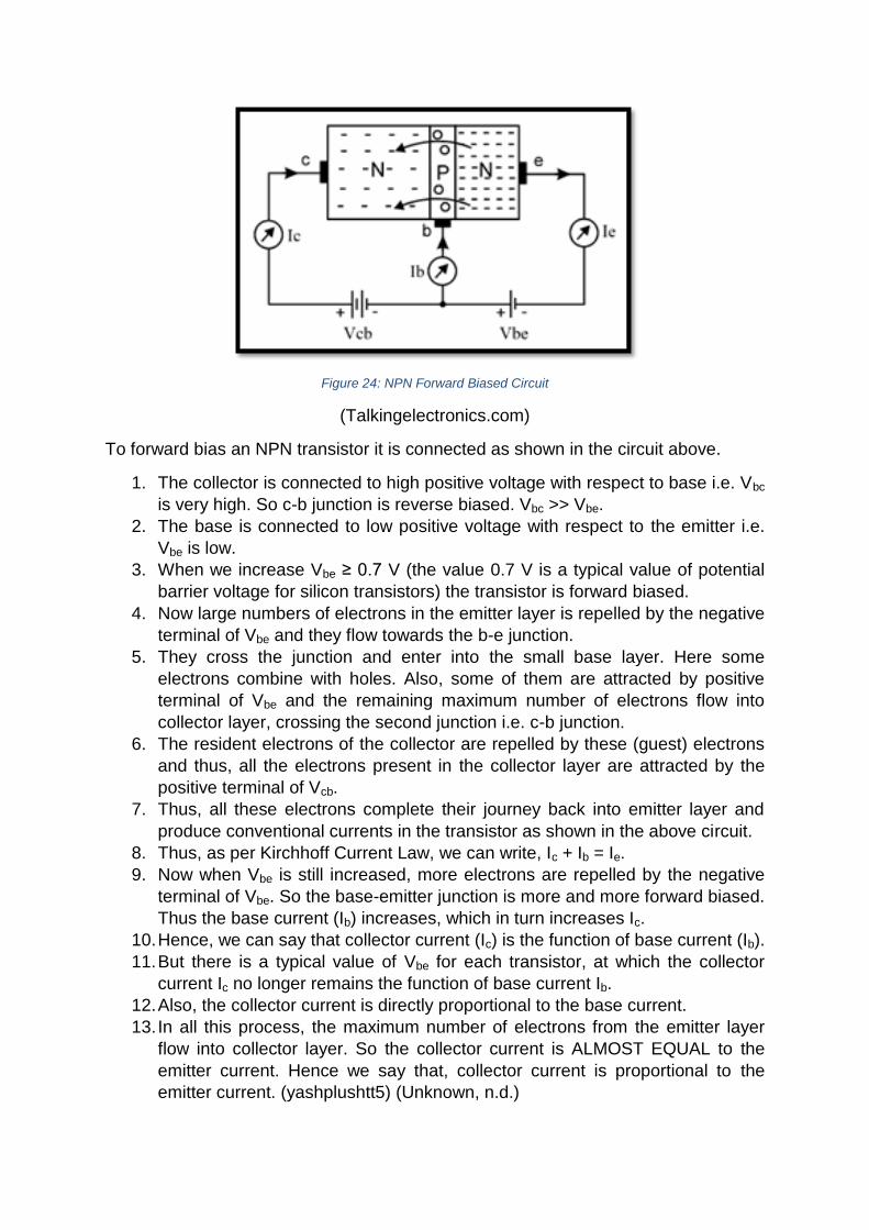
Figure 24: NPN Forward Biased Circuit
(Talkingelectronics.com)
To forward bias an NPN transistor it is connected as shown in the circuit above.
1. The collector is connected to high positive voltage with respect to base i.e. Vbc
is very high. So c-b junction is reverse biased. Vbc >> Vbe.
2. The base is connected to low positive voltage with respect to the emitter i.e.
Vbe is low.
3. When we increase Vbe ≥ 0.7 V (the value 0.7 V is a typical value of potential
barrier voltage for silicon transistors) the transistor is forward biased.
4. Now large numbers of electrons in the emitter layer is repelled by the negative
terminal of Vbe and they flow towards the b-e junction.
5. They cross the junction and enter into the small base layer. Here some
electrons combine with holes. Also, some of them are attracted by positive
terminal of Vbe and the remaining maximum number of electrons flow into
collector layer, crossing the second junction i.e. c-b junction.
6. The resident electrons of the collector are repelled by these (guest) electrons
and thus, all the electrons present in the collector layer are attracted by the
positive terminal of Vcb.
7. Thus, all these electrons complete their journey back into emitter layer and
produce conventional currents in the transistor as shown in the above circuit.
8. Thus, as per Kirchhoff Current Law, we can write, Ic + Ib = Ie.
9. Now when Vbe is still increased, more electrons are repelled by the negative
terminal of Vbe. So the base-emitter junction is more and more forward biased.
Thus the base current (Ib) increases, which in turn increases Ic.
10. Hence, we can say that collector current (Ic) is the function of base current (Ib).
11. But there is a typical value of Vbe for each transistor, at which the collector
current Ic no longer remains the function of base current Ib.
12. Also, the collector current is directly proportional to the base current.
13. In all this process, the maximum number of electrons from the emitter layer
flow into collector layer. So the collector current is ALMOST EQUAL to the
emitter current. Hence we say that, collector current is proportional to the
emitter current. (yashplushtt5) (Unknown, n.d.)

14.6.5. Reverse Biasing
Figure 25: NPN Reverse Biased Circuit
(Talkingelectronics.com)
In this method both the junctions are reverse biased as the batteries are connected
in opposite direction as shown in the diagram above. Due to the Vcb battery, the
collector-base junction is reverse biased. Similarly, due to the Vcb battery, the base-
emitter junction is also reverse biased. So charges cannot flow and current in the
transistor is practically zero. This method is not useful as the transistor is in “cut-off”
state since the base current is zero.
14.6.6. NPN Input Curve
(Talkingelectronics.com)
Figure 26: NPN Input Curve
Figure 26, shows the base emitter voltage against the base emitter current. IBE/VBE
shows the input CONDUCTANCE of the transistor. As conductance I / V is the
reciprocal of RESISTANCE (V / I) this curve can be used to determine the input
resistance of the transistor. The steepness of this particular curve when the VBE is

above 1 volt shows that the input conductance is very high, and there is a large
increase in current (in practice, usually enough to destroy the transistor!) for a very
small increase in VBE. Therefore the input RESISTANCE must be low. Around 0.6 to
0.7 volts the graph curves shows that the input resistance of a transistor varies,
according to the amount of base current flowing, and below about 0.5 volts base
current ceases.
14.6.7. NPN Output Curve
(Talkingelectronics.com)
Figure 27: NPN Output Curve
Figure 27, shows the output characteristic curve of the NPN Transistor. The near
horizontal parts of the graph lines show that a change in collector emitter voltage VCE
has almost no effect on collector current in this region. Therefore the graph shows
that the output resistance of the transistor is high.
14.6.7.1. The Transistor Characteristic Curve
Figure 28, below provides us with a graphical representation of the comparison
between a simple transistor circuit and its characteristic curve.
Figure 28: Characteristic Curve
14.6.8. Regions of Operation
The transistor is divided into 3 distinct regions. The active region is where the
transistor operates as an amplifier.
In the saturation region the transistor is fully switched on and Ib has no effect on the
magnitude of Ic. In the cut-off region the transistor is switched off. When the
transistor is used as a switch it operates in these two regions.
(E-Learning)
Figure 29: Regions of Operation
14.6.9. The transistor DC Load Line
(E-Learning)
Figure 30: DC Load Line
From the characteristic curve we can see that transistor can safely handle 12 V
across its collector emitter terminals, and a collector current of 70 mA. When these
two points are joined by a straight line it is termed the DC Load Line of the transistor.
The load line is an imaginary straight line along which the operating point moves up
and down. The Q-point (quiescent point) is the steady state operating point of the
transistor and it is chosen at the middle of the load line.
From this diagram it is evident that the DC Load line provides us with a tool to
determine the characteristics of the output signal of the amplifier. Below are just a
few characteristics of a transistor that can be determined from the load line:
1. The load line can be used to determine the parameters within which the
transistor can be operated.
2. The Q-Point is determined by the DC Biasing circuit of the transistor.
3. By changing the supply voltage the load line can be shifted in parallel.
4. The load line can be used to determine the AC current, voltage and power
gain of the signal that is applied to the base of the transistor.
14.6.10. Transistor Power related to the load line
(E-Learning)
Figure 31: Transistor DC Load line with Q-Point
From the diagram above it can be seen that the transistor operates optimally at
40𝑚𝐴 and 6V. These values are taken at the center of the characteristic curve at the
point the Q-Point intersects the load line. Apart from helping us obtain the optimal
operating point of the transistor, these two value can also help us calculate the
Power dissipated by the transistor. Since Power is the product of current and
voltage, similarly if these two values are multiplied they help us obtain the Power of
the Transistor. For the transistor represented in Figure 31 above, its Power can be
calculated as follows:
Transisitor Power (P) = ICQ × VCQ
= 40mA × 6V
ICQ and VCQ are the transistors respective current and voltage values at the Q − Point
14.6.11. Influence of the DC Load Line on the Characteristics
of a Transistor
Figure 32: DC Load line with Q-Point of Transistor.
The slope of the load line invariably has an effect on the transistor. Similarly the
position of the Q-Point has an effect on the characteristics of the transistor. The
position of the Q Point on the DC load line determines the maximum signal that we
can get from the circuit before clipping can occur. Figure 32 (a) shows the Q-point
near the cut off region. Here the signal starts to clip at point A. This is called cut off
clipping. In Figure 32 (b) the Q Point is located near the saturation region. Clipping
now starts at point B. This is caused by the close proximity to the saturation region.
Figure 32 (c) has the Q point at the centre of the load line. In this condition we get
the maximum possible output signal. The signal at this point is undistorted.
The position of the Q point and slope of the load line play an important part in the
use of a transistor for amplification purposes as it determines what type of amplifier
the transistor can be used for.
14.6.12. Transistor Symbols
Figure 33: NPN Transistor Symbol
Figure 34: PNP Transistor Symbol

14.7. Transistor Applications
14.7.1. The Transistor as a Switch
The transistor can be used as an electronic switch. Such switches are used in
computer circuits and logic circuits to supply low and high voltage levels.
In Figure 35, when the switch is open there is no current to the base, so the
transistor is in the cut off condition with no collector current. The entire voltage drop
is across the transistor.
The base resistor is chosen small enough so that the base current drives the
transistor into saturation.
In this example the mechanical switch is used to produce the base current to close
the transistor switch to show the principles. In practice, any voltage on the base
sufficient to drive the transistor to saturation will close the switch and light the bulb.
(Hyperphysics)
Figure 35: The Transistor as a switch
14.7.2. Transistor as an Amplifier
The common-emitter amplifier is designed so that a small change in voltage (Vin)
changes the small current through the base of the transistor; the transistor's current
amplification combined with the properties of the circuit mean that small alterations in
Vin produce large changes in Vout.
Various configurations of single transistor amplifier are possible, with some providing
current gain, some voltage gain, and some both.
From mobile phones to televisions, vast numbers of products include amplifiers for
sound reproduction, radio transmission, and signal processing. The first discreet-
transistor audio amplifiers barely supplied a few hundred mill watts, but power and
audio fidelity gradually increased as better transistors became available and
amplifier architecture evolved.
Modern transistor audio amplifiers of up to a few hundred watts are common and
relatively inexpensive.
(Wikipedia)
Figure 36: Common emitter amplifier
14.7.3. Transistor Gain
The number of times an input signal is amplified is called Gain. If only voltage has
been amplified it is called voltage gain and if only current has been amplified it is
called current gain. It is often expressed using the logarithmic decibel (dB) units ("dB
gain"). The symbol “A” is usually associated with gain.
AP= Power gain
AV= Voltage gain
AI= Current gain
Usually we are interested in power gain (AP). Since gain is only a ratio between
similar parameters, it has no units.
𝐏𝐨𝐰𝐞𝐫 𝐆𝐚𝐢𝐧 =𝐎𝐮𝐭𝐩𝐮𝐭 𝐏𝐨𝐰𝐞𝐫
𝐈𝐧𝐩𝐮𝐭 𝐏𝐨𝐰𝐞𝐫
𝐕𝐨𝐥𝐭𝐚𝐠𝐞 𝐆𝐚𝐢𝐧 =𝐎𝐮𝐭𝐩𝐮𝐭 𝐕𝐨𝐥𝐭𝐚𝐠𝐞
𝐈𝐧𝐩𝐮𝐭 𝐕𝐨𝐥𝐭𝐚𝐠𝐞
𝐂𝐮𝐫𝐫𝐞𝐧𝐭 𝐆𝐚𝐢𝐧 =𝐎𝐮𝐭𝐩𝐮𝐭 𝐂𝐮𝐫𝐫𝐞𝐧𝐭
𝐈𝐧𝐩𝐮𝐭 𝐂𝐮𝐫𝐫𝐞𝐧𝐭
14.7.4. Current Gain
The current flowing between emitter and collector of a transistor is much greater than
that flowing between base and emitter. So a small base current is controlling the
much larger collector current. The ratio of the two currents, IC / IB is constant,
provided that the collector emitter voltage VCE is constant. Therefore, if the base
current rises, so does collector current.
This ratio is the current gain of the transistor and is given the symbol hfe. A fairly low
gain transistor might have a current gain of 20 to 50, while a high gain type may
have a gain of 300 to 800 or more. The spread of values of hfe for any given
transistor is quite large, even in transistors of the same type and batch.
14.7.5. Voltage Gain
As mentioned earlier, gain is the amplification factor of the transistor. The number of
times an input signal is amplified is called the gain of the amplifier. Voltage gain is
thus the number of times the voltage is amplified in an amplifier. It is given by the
formula:
𝐴𝑉 =𝑂𝑢𝑡𝑝𝑢𝑡 𝑉𝑜𝑙𝑡𝑎𝑔𝑒
𝐼𝑛𝑝𝑢𝑡 𝑉𝑜𝑙𝑡𝑎𝑔𝑒
𝐴𝑉 =𝑉𝑜𝑢𝑡𝑉𝑖𝑛
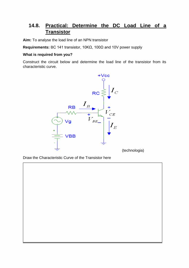
14.8. Practical: Determine the DC Load Line of a
Transistor
Aim: To analyse the load line of an NPN transistor
Requirements: BC 141 transistor, 10KΩ, 100Ω and 10V power supply
What is required from you?
Construct the circuit below and determine the load line of the transistor from its
characteristic curve.
(technologia)
Draw the Characteristic Curve of the Transistor here
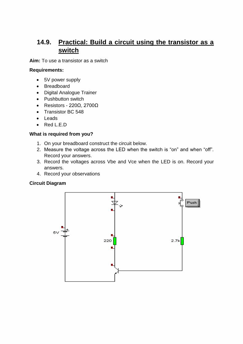
14.9. Practical: Build a circuit using the transistor as a
switch
Aim: To use a transistor as a switch
Requirements:
5V power supply
Breadboard
Digital Analogue Trainer
Pushbutton switch
Resistors - 220Ω, 2700Ω
Transistor BC 548
Leads
Red L.E.D
What is required from you?
1. On your breadboard construct the circuit below.
2. Measure the voltage across the LED when the switch is “on” and when “off”.
Record your answers.
3. Record the voltages across Vbe and Vce when the LED is on. Record your
answers.
4. Record your observations
Circuit Diagram

Measurements
Voltage across LED – ON
Voltage across LED – OFF
Vbe when LED ON
Vbe when LED OFF
Vce when LED ON
Vce when LED OFF
Observations
____________________________________
____________________________________
____________________________________
____________________________________
____________________________________
____________________________________
____________________________________
____________________________________
____________________________________
14.10. The PNP Transistor
14.10.1. Construction
The only way that the PNP-transistor is different from the NPN-transistor is that the
base is connected to the n-type material and the collector and emitter are the p-type
materials.
The emitter is connected to the positive. The collector is connected to the negative.
When a negative voltage is connected to the base and it is sufficient in size to the
forward bias the base-emitter pn-junction (Si = 0.6 V and Ge = 0.3 V), the transistor
will become conductive. Electrons moves from the base to the emitter. The influx of
minority carriers into the base will forward bias the base-collector junction. When this
happens, current will flow from the collector to the base and through the emitter to
the positive supply.
Symbol
Figure 37: Composition
14.10.2. Principle of Operation
The PNP transistor works essentially the same as the NPN transistor. However,
since the emitter, base, and collector in the PNP transistor are made of materials
that are different from those used in the NPN transistor, different current carriers flow
in the PNP unit. The majority current carriers in the PNP transistor are holes. This is
in contrast to the NPN transistor where the majority current carriers are electrons. To
support this different type of current (hole flow), the bias batteries are reversed for
the PNP transistor. A typical bias setup for the PNP transistor is shown in Figure 38.

Notice that the procedure used to properly bias the NPN transistor also applies here
to the PNP transistor. The first letter (p) in the PNP sequence indicates the polarity of
the voltage required for the emitter (positive), and the second letter (n) indicates the
polarity of the base voltage (negative). Since the base-collector junction is always
reverse biased, then the opposite polarity voltage (negative) must be used for the
collector. Thus, the base of the PNP transistor must be negative with respect to the
emitter, and the collector must be more negative than the base. Remember, just as
in the case of the NPN transistor, this difference in supply voltage is necessary to
have current flow (hole flow in the case of the PNP transistor) from the emitter to the
collector. Although hole flow is the predominant type of current flow in the PNP
transistor, hole flow only takes place within the transistor itself, while electrons flow in
the external circuit. However, it is the internal hole flow that leads to electron flow in
the external wires connected to the transistor.
Figure 38: PNP Biasing
Now let us consider what happens when the emitter-base junction is forward
biased.
1. With the bias setup as shown in Figure 38 above, the positive terminal of the
battery repels the emitter holes toward the base, while the negative terminal drives
the base electrons toward the emitter.
2. When an emitter hole and a base electron meet, they combine. For each electron
that combines with a hole, another electron leaves the negative terminal of the
battery, and enters the base.
3. At the same time, an electron leaves the emitter, creating a new hole and enters
the positive terminal of the battery. This movement of electrons into the base and out
of the emitter constitutes base current flow (IB), and the path these electrons take is
referred to as the emitter-base circuit.
4. In the reverse-biased junction, the negative voltage on the collector and the
positive voltage on the base block the majority current carriers from crossing the
junction.
5. This same negative collector voltage acts as forward bias for the minority current
holes in the base, which cross the junction and enter the collector. The minority
current electrons in the collector also sense forward bias-the positive base voltage-
and move into the base.
6. The holes in the collector are filled by electrons that flow from the negative
terminal of the battery. At the same time the electrons leave the negative terminal of
the battery, other electrons in the base break their covalent bonds and enter the
positive terminal of the battery. Although there is only minority current flow in the
reverse-biased junction, it is still very small because of the limited number of minority
current carriers.
7. The interaction between the forward- and reverse-biased junctions in a PNP transistor is very similar to that in an NPN transistor, except that in the PNP transistor, the majority current carriers are holes.
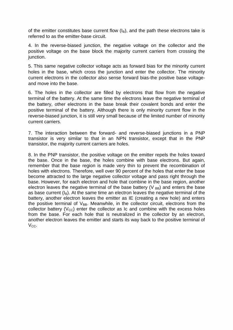
8. In the PNP transistor, the positive voltage on the emitter repels the holes toward the base. Once in the base, the holes combine with base electrons. But again, remember that the base region is made very thin to prevent the recombination of holes with electrons. Therefore, well over 90 percent of the holes that enter the base become attracted to the large negative collector voltage and pass right through the base. However, for each electron and hole that combine in the base region, another electron leaves the negative terminal of the base battery (V BB) and enters the base as base current (IB). At the same time an electron leaves the negative terminal of the battery, another electron leaves the emitter as IE (creating a new hole) and enters the positive terminal of VBB. Meanwhile, in the collector circuit, electrons from the collector battery (VCC) enter the collector as Ic and combine with the excess holes from the base. For each hole that is neutralized in the collector by an electron, another electron leaves the emitter and starts its way back to the positive terminal of VCC.
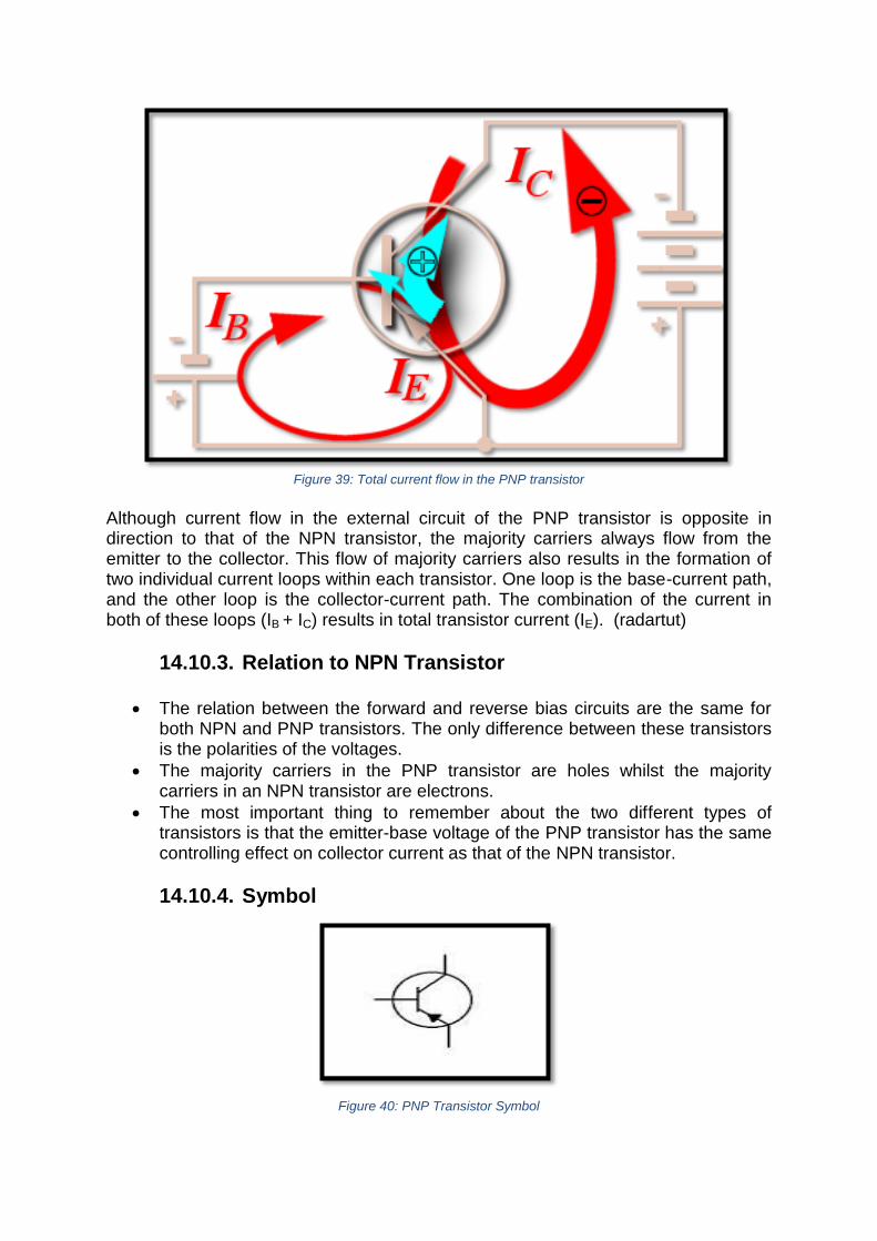
Figure 39: Total current flow in the PNP transistor
Although current flow in the external circuit of the PNP transistor is opposite in direction to that of the NPN transistor, the majority carriers always flow from the emitter to the collector. This flow of majority carriers also results in the formation of two individual current loops within each transistor. One loop is the base-current path, and the other loop is the collector-current path. The combination of the current in both of these loops (IB + IC) results in total transistor current (IE). (radartut)
14.10.3. Relation to NPN Transistor
The relation between the forward and reverse bias circuits are the same for both NPN and PNP transistors. The only difference between these transistors is the polarities of the voltages.
The majority carriers in the PNP transistor are holes whilst the majority carriers in an NPN transistor are electrons.
The most important thing to remember about the two different types of transistors is that the emitter-base voltage of the PNP transistor has the same controlling effect on collector current as that of the NPN transistor.
14.10.4. Symbol
Figure 40: PNP Transistor Symbol

14.10.5. Applications
The PNP transistor has the same applications as the NPN transistor. Some of its
applications include:
1. Switching circuits
2. Amplifiers.
14.10.5.1. Sample Circuits
Figure 41: The PNP Transistor being used as a switch
Figure 42: The PNP Transistor being used as an amplifier
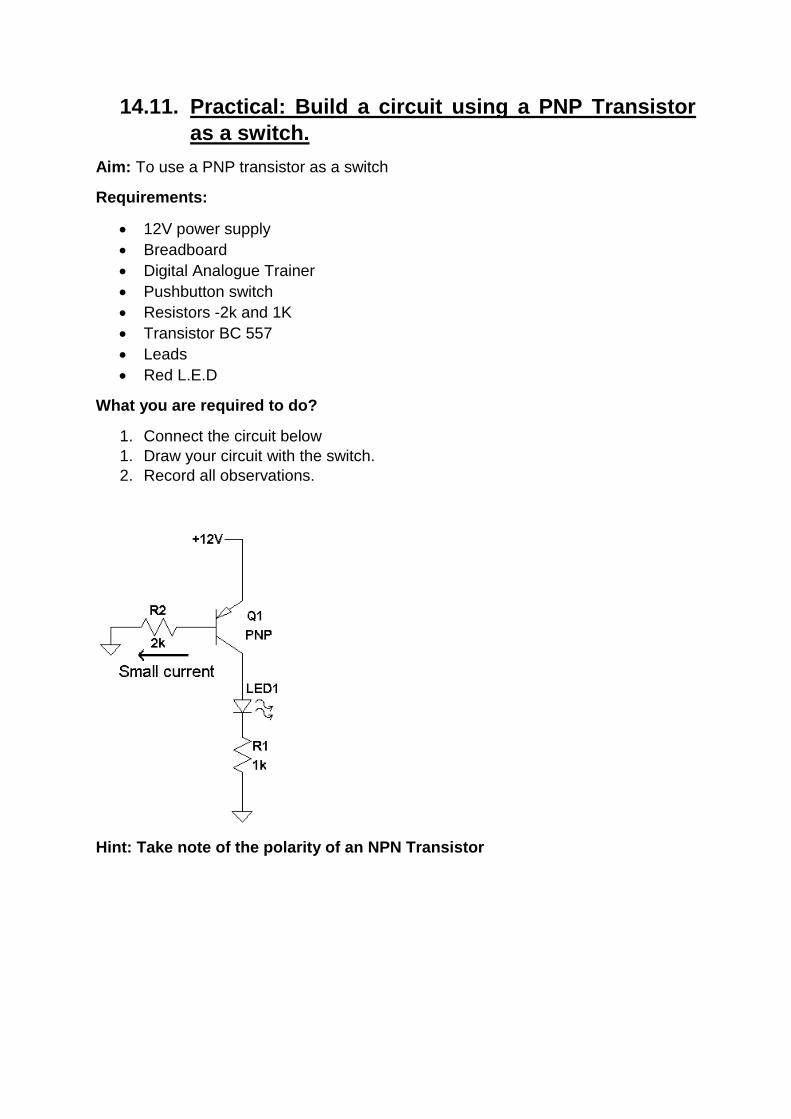
14.11. Practical: Build a circuit using a PNP Transistor
as a switch.
Aim: To use a PNP transistor as a switch
Requirements:
12V power supply
Breadboard
Digital Analogue Trainer
Pushbutton switch
Resistors -2k and 1K
Transistor BC 557
Leads
Red L.E.D
What you are required to do?
1. Connect the circuit below
1. Draw your circuit with the switch.
2. Record all observations.
Hint: Take note of the polarity of an NPN Transistor

Circuit Diagram
Observations
________________________________________
________________________________________
________________________________________
________________________________________
________________________________________
14.12. Thyristors – The Silicon Controlled Rectifier
(SCR)
14.13. Thyristors have at least four layers of alternating n- and p-type
materials. They act as bi-stable switches and are activated by applying
a pulse to the gate. Typical examples of Thyristors are The Silicon
Controlled Rectifier (SCR) and The Triac. Thyristors have no
amplification ability; therefore they are used in switching circuits only.
Their characteristics make them particularly useful in power control
circuits such as motor speed control and light dimmers.
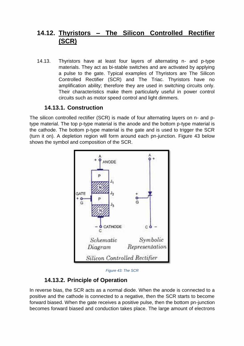
14.13.1. Construction
The silicon controlled rectifier (SCR) is made of four alternating layers on n- and p-
type material. The top p-type material is the anode and the bottom p-type material is
the cathode. The bottom p-type material is the gate and is used to trigger the SCR
(turn it on). A depletion region will form around each pn-junction. Figure 43 below
shows the symbol and composition of the SCR.
Figure 43: The SCR
14.13.2. Principle of Operation
In reverse bias, the SCR acts as a normal diode. When the anode is connected to a
positive and the cathode is connected to a negative, then the SCR starts to become
forward biased. When the gate receives a positive pulse, then the bottom pn-junction
becomes forward biased and conduction takes place. The large amount of electrons
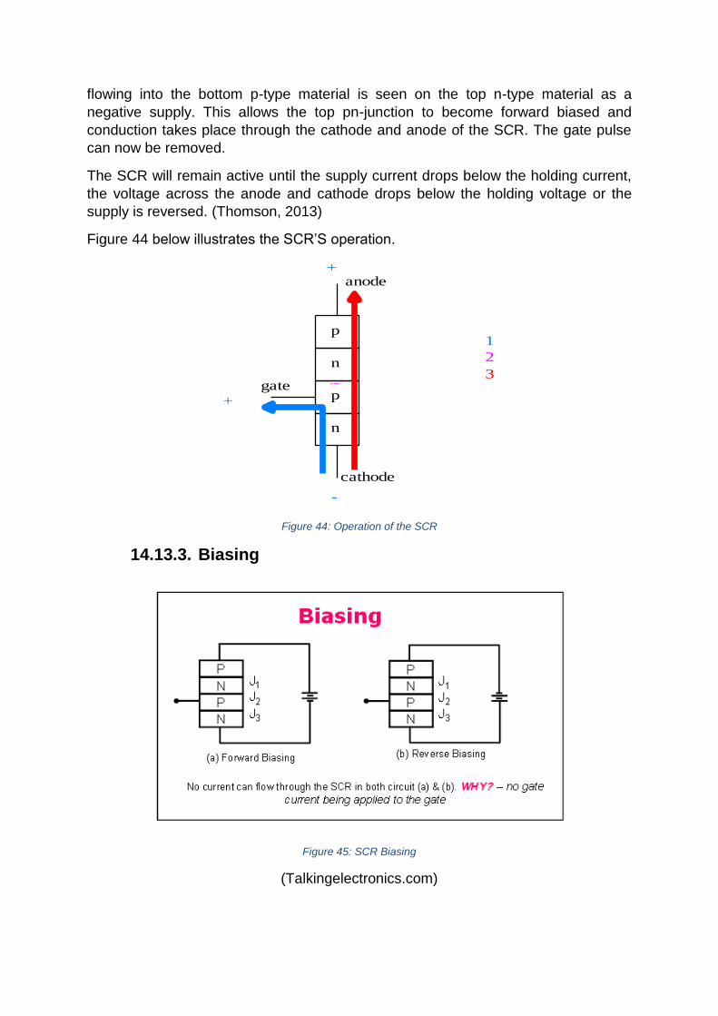
flowing into the bottom p-type material is seen on the top n-type material as a
negative supply. This allows the top pn-junction to become forward biased and
conduction takes place through the cathode and anode of the SCR. The gate pulse
can now be removed.
The SCR will remain active until the supply current drops below the holding current,
the voltage across the anode and cathode drops below the holding voltage or the
supply is reversed. (Thomson, 2013)
Figure 44 below illustrates the SCR’S operation.
p
n
p
n
anode
cathode
gate
1
+
+
-
---3
2
Figure 44: Operation of the SCR
14.13.3. Biasing
Figure 45: SCR Biasing
(Talkingelectronics.com)
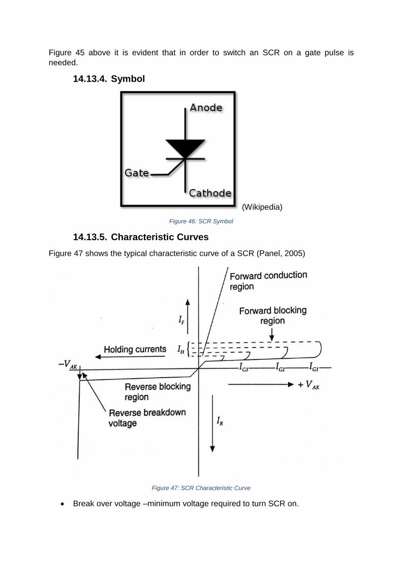
Figure 45 above it is evident that in order to switch an SCR on a gate pulse is
needed.
14.13.4. Symbol
(Wikipedia)
Figure 46: SCR Symbol
14.13.5. Characteristic Curves
Figure 47 shows the typical characteristic curve of a SCR (Panel, 2005)
Figure 47: SCR Characteristic Curve
Break over voltage –minimum voltage required to turn SCR on.
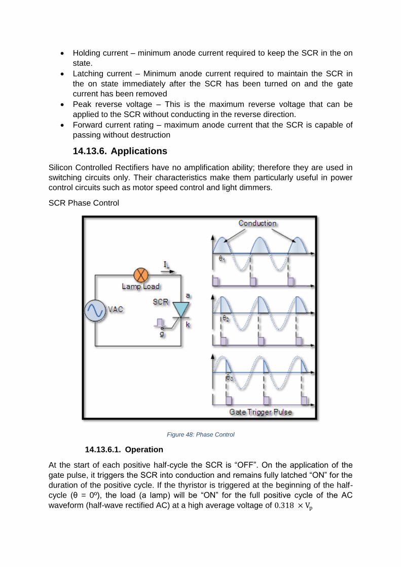
Holding current – minimum anode current required to keep the SCR in the on
state.
Latching current – Minimum anode current required to maintain the SCR in
the on state immediately after the SCR has been turned on and the gate
current has been removed
Peak reverse voltage – This is the maximum reverse voltage that can be
applied to the SCR without conducting in the reverse direction.
Forward current rating – maximum anode current that the SCR is capable of
passing without destruction
14.13.6. Applications
Silicon Controlled Rectifiers have no amplification ability; therefore they are used in
switching circuits only. Their characteristics make them particularly useful in power
control circuits such as motor speed control and light dimmers.
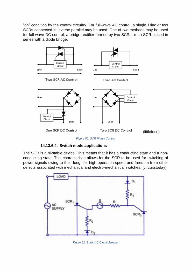
SCR Phase Control
Figure 48: Phase Control
14.13.6.1. Operation
At the start of each positive half-cycle the SCR is “OFF”. On the application of the
gate pulse, it triggers the SCR into conduction and remains fully latched “ON” for the
duration of the positive cycle. If the thyristor is triggered at the beginning of the half-
cycle (θ = 0º), the load (a lamp) will be “ON” for the full positive cycle of the AC
waveform (half-wave rectified AC) at a high average voltage of 0.318 × Vp

As the application of the trigger pulse increases along the half-cycle (θ = 0º to 90º),
the lamp is illuminated for less time and the average voltage delivered to the lamp
will also be proportionally less reducing its brightness.
We can therefore use a silicon controlled rectifier as an AC light dimmer as well as in
a variety of other AC power applications such as: AC motor-speed control,
temperature control systems and power regulator circuits, etc.
Thus far we have seen that a thyristor is essentially a half-wave device that conducts
in only the positive half of the cycle when the Anode is positive and blocks current
flow like a diode when the Anode is negative, irrespective of the Gate signal.
14.13.6.2. The SCR as a Relaxation Oscillator
In electronics a relaxation oscillator is a nonlinear electronic oscillator circuit that
produces a non-sinusoidal repetitive output signal, such as a triangle wave or square
wave.
Circuit Diagram
Figure 49: Relaxation oscillator Circuit
From the circuit, when power is applied, capacitor Ct charges and the voltage across
resistor RT decreases. When the voltage across RT drops to 0.6 V less the gate
voltage, the SCR turns on. This is the cathode voltage of the SCR. This turn-on
produces current flow through CT and a voltage spike across R3.
Since the large value of RT prevents there being sufficient current to maintain
conduction, the SCR immediately turns off, and RT begins its charge cycle again.
14.13.6.3. Phase Control
Phase control is the most common form of Thyristor power control. The Thyristor is
held in the off condition, that is, all current flow in the circuit is blocked by the
Thyristor except a minute leakage current. Then the Thyristor is triggered into an
“on” condition by the control circuitry. For full-wave AC control, a single Triac or two
SCRs connected in inverse parallel may be used. One of two methods may be used
for full-wave DC control, a bridge rectifier formed by two SCRs or an SCR placed in
series with a diode bridge.
(littlefuse)
Figure 50: SCR Phase Control
14.13.6.4. Switch mode applications
The SCR is a bi-stable device. This means that it has a conducting state and a non-
conducting state. This characteristic allows for the SCR to be used for switching of
power signals owing to their long life, high operation speed and freedom from other
defects associated with mechanical and electro-mechanical switches. (circuitstoday)
Figure 51: Static AC Circuit Breaker
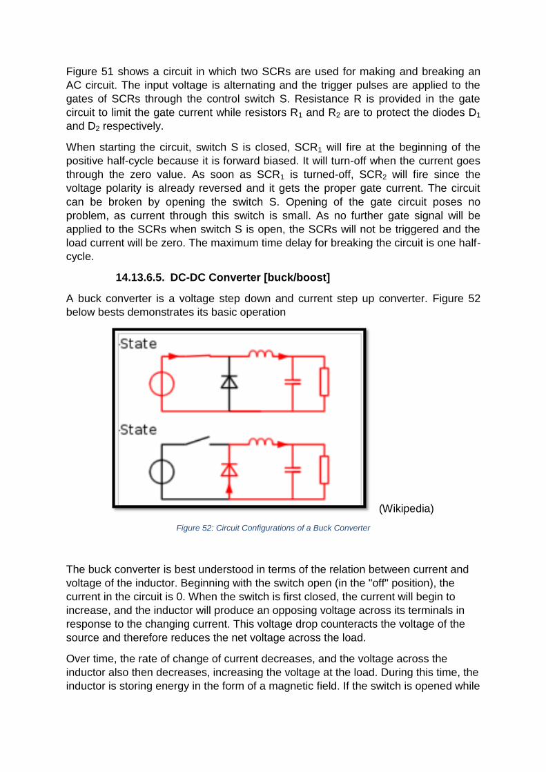
Figure 51 shows a circuit in which two SCRs are used for making and breaking an
AC circuit. The input voltage is alternating and the trigger pulses are applied to the
gates of SCRs through the control switch S. Resistance R is provided in the gate
circuit to limit the gate current while resistors R1 and R2 are to protect the diodes D1
and D2 respectively.
When starting the circuit, switch S is closed, SCR1 will fire at the beginning of the
positive half-cycle because it is forward biased. It will turn-off when the current goes
through the zero value. As soon as SCR1 is turned-off, SCR2 will fire since the
voltage polarity is already reversed and it gets the proper gate current. The circuit
can be broken by opening the switch S. Opening of the gate circuit poses no
problem, as current through this switch is small. As no further gate signal will be
applied to the SCRs when switch S is open, the SCRs will not be triggered and the
load current will be zero. The maximum time delay for breaking the circuit is one half-
cycle.
14.13.6.5. DC-DC Converter [buck/boost]
A buck converter is a voltage step down and current step up converter. Figure 52
below bests demonstrates its basic operation
(Wikipedia)
Figure 52: Circuit Configurations of a Buck Converter
The buck converter is best understood in terms of the relation between current and
voltage of the inductor. Beginning with the switch open (in the "off" position), the
current in the circuit is 0. When the switch is first closed, the current will begin to
increase, and the inductor will produce an opposing voltage across its terminals in
response to the changing current. This voltage drop counteracts the voltage of the
source and therefore reduces the net voltage across the load.
Over time, the rate of change of current decreases, and the voltage across the
inductor also then decreases, increasing the voltage at the load. During this time, the
inductor is storing energy in the form of a magnetic field. If the switch is opened while

the current is still changing, then there will always be a voltage drop across the
inductor, so the net voltage at the load will always be less than the input voltage
source.
When the switch is opened again, the voltage source will be removed from the
circuit, and the current will decrease. The changing current will produce a change in
voltage across the inductor, now aiding the source voltage. The stored energy in the
inductor's magnetic field supports current flow through the load. During this time, the
inductor is discharging its stored energy into the rest of the circuit. If the switch is
closed again before the inductor fully discharges, the voltage at the load will always
be greater than zero.
The switch in a Buck Converter is replaced by a SCR due to its ability to have
switching applications.
Figure 53: Buck Converter using a SCR
(NPTEL)
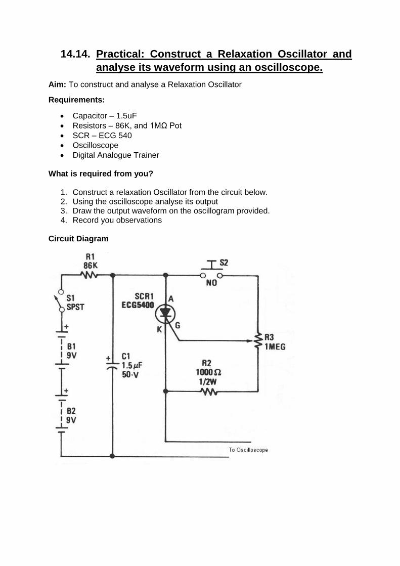
14.14. Practical: Construct a Relaxation Oscillator and
analyse its waveform using an oscilloscope.
Aim: To construct and analyse a Relaxation Oscillator
Requirements:
Capacitor – 1.5uF
Resistors – 86K, and 1MΩ Pot
SCR – ECG 540
Oscilloscope
Digital Analogue Trainer What is required from you?
1. Construct a relaxation Oscillator from the circuit below. 2. Using the oscilloscope analyse its output 3. Draw the output waveform on the oscillogram provided. 4. Record you observations
Circuit Diagram
Oscillogram
Observations
________________________________________
________________________________________
________________________________________
________________________________________
________________________________________
________________________________________
________________________________________
________________________________________

14.15. Practical: Construct a Light Dimmer Circuit using
an SCR
Aim: To connect an SCR in light dimming circuit
Requirements:
Power supply 6V AC
Bread Board
47K Pre-set resistor / POT
1𝑢𝐹 Capacitor
Diode 1N4007
6 V Lamp
SCR – CMR 106-4
Hook up Leads
Circuit Diagram
Connect the circuit as shown above.
Observation
__________________________________________________
__________________________________________________
__________________________________________________
__________________________________________________
__________________________________________________
________________________________________________
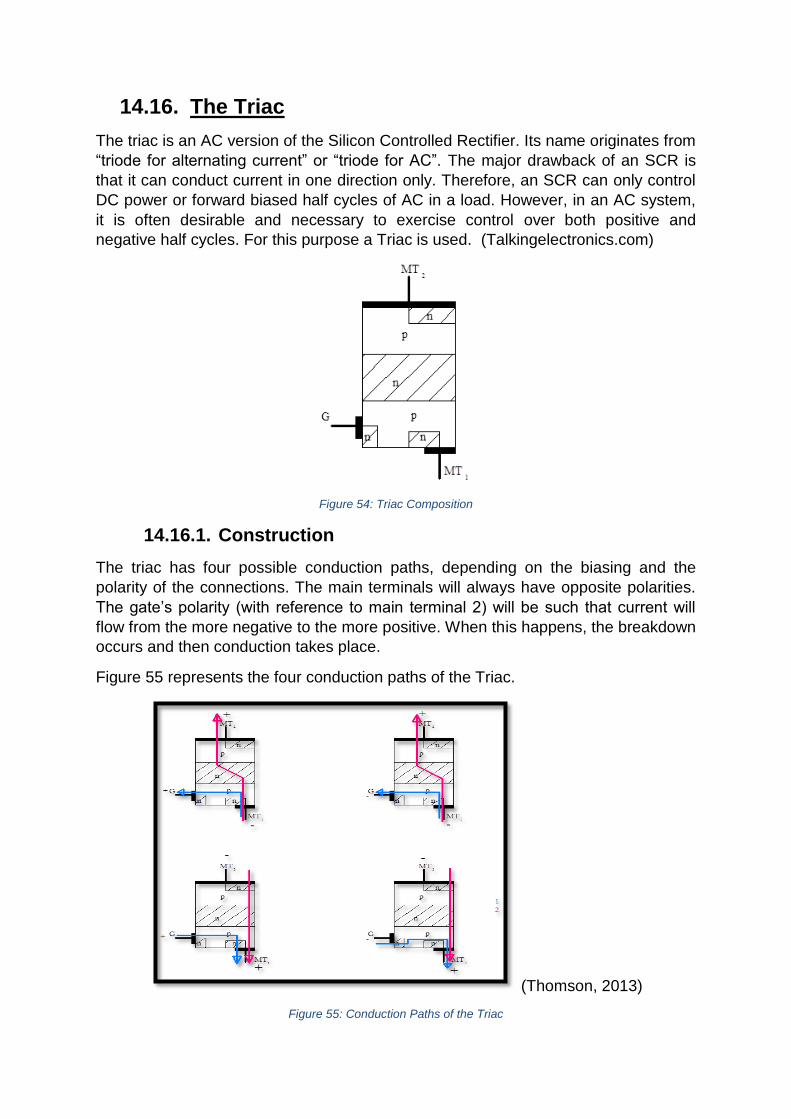
14.16. The Triac
The triac is an AC version of the Silicon Controlled Rectifier. Its name originates from
“triode for alternating current” or “triode for AC”. The major drawback of an SCR is
that it can conduct current in one direction only. Therefore, an SCR can only control
DC power or forward biased half cycles of AC in a load. However, in an AC system,
it is often desirable and necessary to exercise control over both positive and
negative half cycles. For this purpose a Triac is used. (Talkingelectronics.com)
Figure 54: Triac Composition
14.16.1. Construction
The triac has four possible conduction paths, depending on the biasing and the
polarity of the connections. The main terminals will always have opposite polarities.
The gate’s polarity (with reference to main terminal 2) will be such that current will
flow from the more negative to the more positive. When this happens, the breakdown
occurs and then conduction takes place.
Figure 55 represents the four conduction paths of the Triac.
(Thomson, 2013)
Figure 55: Conduction Paths of the Triac
14.16.2. Principle of Operation
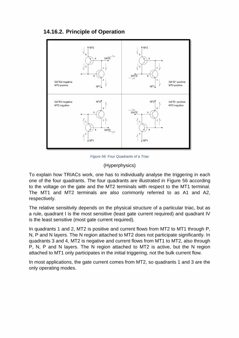
Figure 56: Four Quadrants of a Triac
(Hyperphysics)
To explain how TRIACs work, one has to individually analyse the triggering in each
one of the four quadrants. The four quadrants are illustrated in Figure 56 according
to the voltage on the gate and the MT2 terminals with respect to the MT1 terminal.
The MT1 and MT2 terminals are also commonly referred to as A1 and A2,
respectively.
The relative sensitivity depends on the physical structure of a particular triac, but as
a rule, quadrant I is the most sensitive (least gate current required) and quadrant IV
is the least sensitive (most gate current required).
In quadrants 1 and 2, MT2 is positive and current flows from MT2 to MT1 through P,
N, P and N layers. The N region attached to MT2 does not participate significantly. In
quadrants 3 and 4, MT2 is negative and current flows from MT1 to MT2, also through
P, N, P and N layers. The N region attached to MT2 is active, but the N region
attached to MT1 only participates in the initial triggering, not the bulk current flow.
In most applications, the gate current comes from MT2, so quadrants 1 and 3 are the
only operating modes.
(Hyperphysics)
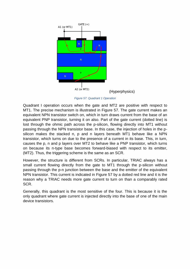
Figure 57: Quadrant 1 Operation
Quadrant I operation occurs when the gate and MT2 are positive with respect to
MT1. The precise mechanism is illustrated in Figure 57. The gate current makes an
equivalent NPN transistor switch on, which in turn draws current from the base of an
equivalent PNP transistor, turning it on also. Part of the gate current (dotted line) is
lost through the ohmic path across the p-silicon, flowing directly into MT1 without
passing through the NPN transistor base. In this case, the injection of holes in the p-
silicon makes the stacked n, p and n layers beneath MT1 behave like a NPN
transistor, which turns on due to the presence of a current in its base. This, in turn,
causes the p, n and p layers over MT2 to behave like a PNP transistor, which turns
on because its n-type base becomes forward-biased with respect to its emitter,
(MT2). Thus, the triggering scheme is the same as an SCR.
However, the structure is different from SCRs. In particular, TRIAC always has a
small current flowing directly from the gate to MT1 through the p-silicon without
passing through the p-n junction between the base and the emitter of the equivalent
NPN transistor. This current is indicated in Figure 57 by a dotted red line and it is the
reason why a TRIAC needs more gate current to turn on than a comparably rated
SCR.
Generally, this quadrant is the most sensitive of the four. This is because it is the
only quadrant where gate current is injected directly into the base of one of the main
device transistors.
(Hyperphysics)
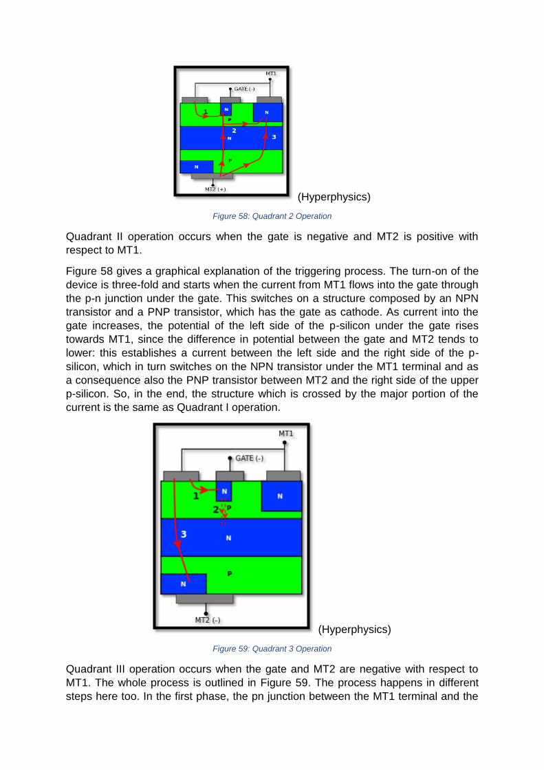
Figure 58: Quadrant 2 Operation
Quadrant II operation occurs when the gate is negative and MT2 is positive with
respect to MT1.
Figure 58 gives a graphical explanation of the triggering process. The turn-on of the
device is three-fold and starts when the current from MT1 flows into the gate through
the p-n junction under the gate. This switches on a structure composed by an NPN
transistor and a PNP transistor, which has the gate as cathode. As current into the
gate increases, the potential of the left side of the p-silicon under the gate rises
towards MT1, since the difference in potential between the gate and MT2 tends to
lower: this establishes a current between the left side and the right side of the p-
silicon, which in turn switches on the NPN transistor under the MT1 terminal and as
a consequence also the PNP transistor between MT2 and the right side of the upper
p-silicon. So, in the end, the structure which is crossed by the major portion of the
current is the same as Quadrant I operation.
(Hyperphysics)
Figure 59: Quadrant 3 Operation
Quadrant III operation occurs when the gate and MT2 are negative with respect to
MT1. The whole process is outlined in Figure 59. The process happens in different
steps here too. In the first phase, the pn junction between the MT1 terminal and the
gate becomes forward-biased (step 1). As forward-biasing implies the injection of
minority carriers in the two layers joining the junction, electrons are injected in the p-
layer under the gate. Some of these electrons do not recombine and escape to the
underlying n-region (step 2). This in turn lowers the potential of the n-region, acting
as the base of a PNP transistor which switches on (turning the transistor on without
directly lowering the base potential is called remote gate control). The lower p-layer
works as the collector of this PNP transistor and has its voltage heightened: actually,
this p-layer also acts as the base of an NPN transistor made up by the last three
layers just over the MT2 terminal, which, in turn, gets activated. Therefore, the red
arrow labelled with a "3" in Figure 59 shows the final conduction path of the current.
(Hyperphysics)
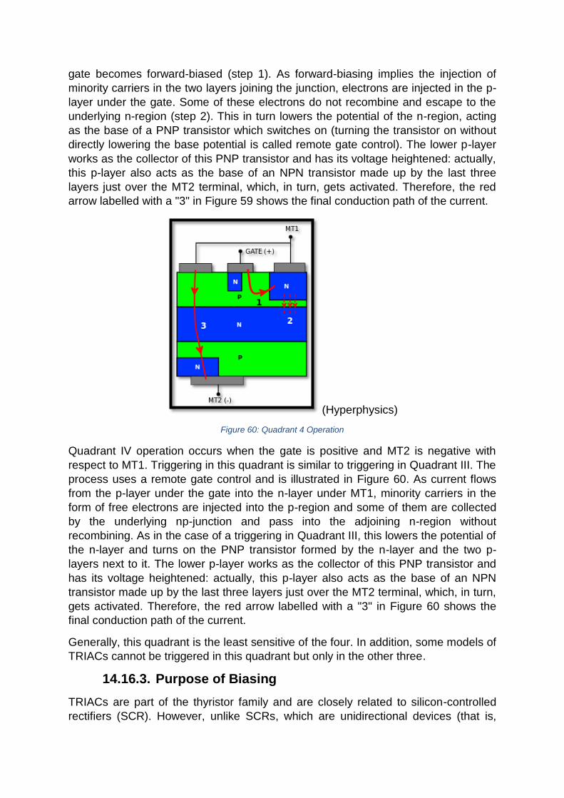
Figure 60: Quadrant 4 Operation
Quadrant IV operation occurs when the gate is positive and MT2 is negative with
respect to MT1. Triggering in this quadrant is similar to triggering in Quadrant III. The
process uses a remote gate control and is illustrated in Figure 60. As current flows
from the p-layer under the gate into the n-layer under MT1, minority carriers in the
form of free electrons are injected into the p-region and some of them are collected
by the underlying np-junction and pass into the adjoining n-region without
recombining. As in the case of a triggering in Quadrant III, this lowers the potential of
the n-layer and turns on the PNP transistor formed by the n-layer and the two p-
layers next to it. The lower p-layer works as the collector of this PNP transistor and
has its voltage heightened: actually, this p-layer also acts as the base of an NPN
transistor made up by the last three layers just over the MT2 terminal, which, in turn,
gets activated. Therefore, the red arrow labelled with a "3" in Figure 60 shows the
final conduction path of the current.
Generally, this quadrant is the least sensitive of the four. In addition, some models of
TRIACs cannot be triggered in this quadrant but only in the other three.
14.16.3. Purpose of Biasing
TRIACs are part of the thyristor family and are closely related to silicon-controlled
rectifiers (SCR). However, unlike SCRs, which are unidirectional devices (that is,

they can conduct current only in one direction), TRIACs are bidirectional and so
current can flow in either direction. Another difference from SCRs is that TRIAC
current flow can be enabled by either a positive or negative current applied to its
gate electrode, whereas SCRs can be triggered only by a positive gate pulse. To
create a triggering current, a positive or negative voltage has to be applied to the
gate with respect to the MT1 terminal (otherwise known as A1).
Once triggered, the device continues to conduct until the current drops below a
certain threshold called the holding current. It is for the reasons outlined above that
biasing plays an integral part in the operation of the Triac.
14.16.4. Symbol
Figure 61; Triac Circuit Symbol
14.16.5. The Triac Characteristic Curve
Figure 62 shows the typical characteristic curve of a triac
(Swart)
Figure 62: Triac Characteristic Curve
Since a triac consists of essentially two SCR’S of opposite orientation fabricated in
the same crystal, its operating characteristics in the first and third quadrants of the
characteristic curve are the same except for the direction of applied voltage and
current flow. The following points can be noted from the characteristic curve:
1. The V-I characteristics for the triac in the 1st and 3rd quadrants are essentially
identical to those of an SCR in the 1st quadrant.
2. The triac can be operated with either a positive or negative gate control
voltage but under normal operation the gate voltage is positive in quadrant 1
and negative in quadrant 3.
3. The supply voltage at which the triac is turned on depends upon the gate
current. The greater the gate current, the smaller the supply voltage at which
the triac is turned on. This allows us to use a triac to control AC power in a
load from 0 to full load power in a smooth and continuous manner with no loss
in the controlling device. (Talkingelectronics.com)
14.16.6. Application
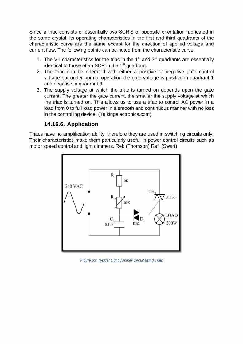
Triacs have no amplification ability; therefore they are used in switching circuits only.
Their characteristics make them particularly useful in power control circuits such as
motor speed control and light dimmers. Ref: (Thomson) Ref: (Swart)
Figure 63: Typical Light Dimmer Circuit using Triac
(Talkingelectronics.com)
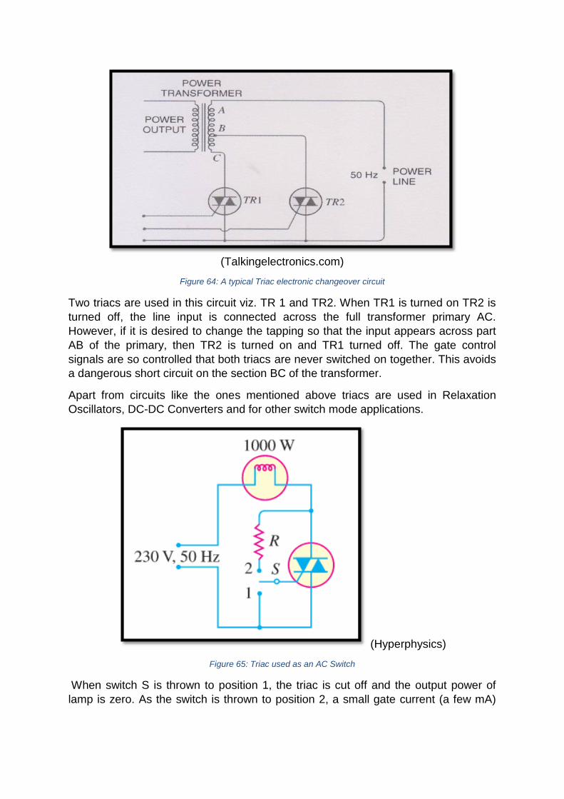
Figure 64: A typical Triac electronic changeover circuit
Two triacs are used in this circuit viz. TR 1 and TR2. When TR1 is turned on TR2 is
turned off, the line input is connected across the full transformer primary AC.
However, if it is desired to change the tapping so that the input appears across part
AB of the primary, then TR2 is turned on and TR1 turned off. The gate control
signals are so controlled that both triacs are never switched on together. This avoids
a dangerous short circuit on the section BC of the transformer.
Apart from circuits like the ones mentioned above triacs are used in Relaxation
Oscillators, DC-DC Converters and for other switch mode applications.
(Hyperphysics)
Figure 65: Triac used as an AC Switch
When switch S is thrown to position 1, the triac is cut off and the output power of
lamp is zero. As the switch is thrown to position 2, a small gate current (a few mA)

flowing through the gate turns the triac on. Consequently, the lamp is switched on to
give full output of 1000 watts.
14.16.7. Circuit Diagrams
(schematicdiagram) Figure 66: A Triac used for Motor Speed Control
(Talkingelectronics.com)
Figure 67: The Triac used in a Simple AC Power Control Circuit

14.17. Practical: Construct a light dimmer circuit
Aim: To construct and examine a light dimmer circuit using a Triac
Requirements:
• Resistors -1K, 220K Pot,
• TIC226- Triac
• D1 – Diac 32 V
• Capacitors -100𝑛𝐹 X 2
• 220V power supply
What are you required to do?
Construct the circuit below.
Observation
____________________________________
____________________________________
____________________________________
____________________________________
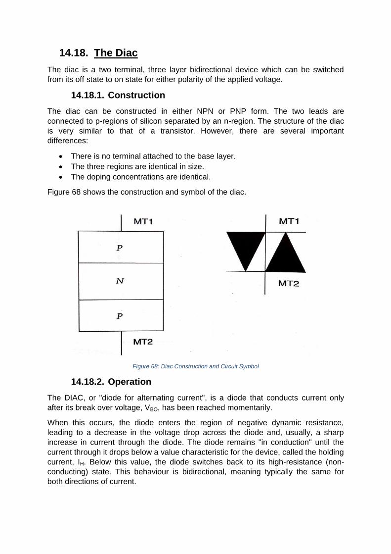
14.18. The Diac
The diac is a two terminal, three layer bidirectional device which can be switched
from its off state to on state for either polarity of the applied voltage.
14.18.1. Construction
The diac can be constructed in either NPN or PNP form. The two leads are
connected to p-regions of silicon separated by an n-region. The structure of the diac
is very similar to that of a transistor. However, there are several important
differences:
There is no terminal attached to the base layer.
The three regions are identical in size.
The doping concentrations are identical.
Figure 68 shows the construction and symbol of the diac.
Figure 68: Diac Construction and Circuit Symbol
14.18.2. Operation
The DIAC, or "diode for alternating current", is a diode that conducts current only
after its break over voltage, VBO, has been reached momentarily.
When this occurs, the diode enters the region of negative dynamic resistance,
leading to a decrease in the voltage drop across the diode and, usually, a sharp
increase in current through the diode. The diode remains "in conduction" until the
current through it drops below a value characteristic for the device, called the holding
current, IH. Below this value, the diode switches back to its high-resistance (non-
conducting) state. This behaviour is bidirectional, meaning typically the same for
both directions of current.

Most DIACs have a three-layer structure with break over voltage around 30 V. Their
behaviour is somewhat similar to that of a neon lamp, but it is much more precisely
controlled and takes place at a lower voltage.
DIACs have no gate electrode, unlike some other thyristors that they are commonly
used to trigger, such as TRIACs. Some TRIACs, like Quadrac, contain a built-in
DIAC in series with the TRIAC's "gate" terminal for this purpose.
DIACs are also called symmetrical trigger diodes due to the symmetry of their
characteristic curve. Because DIACs are bidirectional devices, their terminals are not
labelled as anode and cathode but as A1 and A2 or MT1 ("Main Terminal") and MT2.
14.18.3. Purpose of Biasing
Conduction occurs in a diac when the break over voltage is reached with either
polarity across the two terminals.
Once break over occurs, current is in a direction depending on the polarity of the
voltage across the terminals. The device turns off when the current drops below the
holding value IH.
The equivalent circuit of a diac consists of four transistors arranged as shown below:
(Talkingelectronics.com)
Figure 69: The Equivalent Circuit of a Diac
In the equivalent circuit Q1 and Q2 are forward-biased, and Q3 and Q4 are
reversed-biased. The device operates on the upper right portion of the characteristic
curve under this bias condition.
When the diac is biased as in part (c), the PNPN structure from A2 to A1 is used. In
the equivalent circuit, Q3 and Q4 are forward-biased, and Q1 and Q2 are reverse-
biased. Under this bias condition the device operates on the lower left portion of the
characteristic curve.
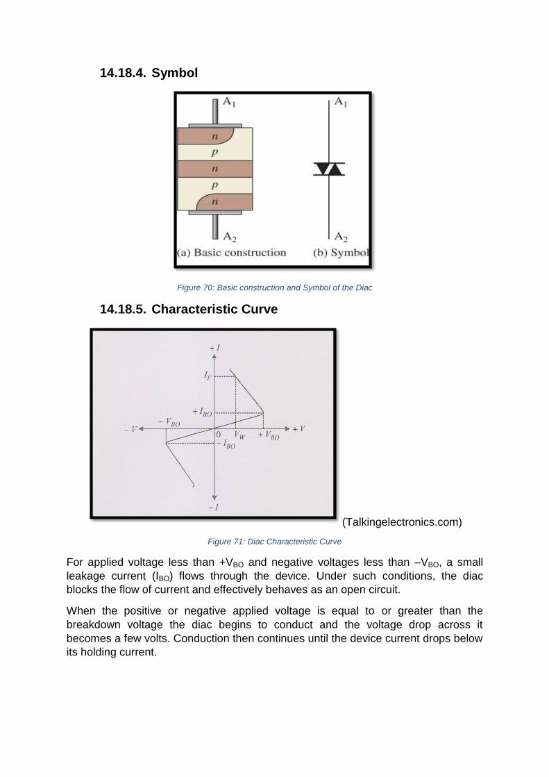
14.18.4. Symbol
Figure 70: Basic construction and Symbol of the Diac
14.18.5. Characteristic Curve
(Talkingelectronics.com)
Figure 71: Diac Characteristic Curve
For applied voltage less than +VBO and negative voltages less than –VBO, a small
leakage current (IBO) flows through the device. Under such conditions, the diac
blocks the flow of current and effectively behaves as an open circuit.
When the positive or negative applied voltage is equal to or greater than the
breakdown voltage the diac begins to conduct and the voltage drop across it
becomes a few volts. Conduction then continues until the device current drops below
its holding current.

14.18.6. Application
Diacs are primarily used for triggering of triacs. Examples of diac applications are:
light dimmer circuits, relaxation oscillators and switch mode applications.
14.18.7. Circuit Diagram Application
A diac used in a light dimmer circuit to trigger a triac
(Talkingelectronics.com)
Figure 72: Diac used in Light Dimmer Circuit
14.19. Homework Exercises
1. What is a datasheet and what is its purpose?
2. Explain the term “Dual in Line Package”
3. Draw diagrams that best represent the differences between Electron Current
Flow and Conventional Current Flow.
4. Define the term “Solid State Device”
5. What is doping and why is it important?
6. Draw a diagram that best represents the PN Junction. Show all majority and
minority carriers.
7. Draw the characteristic curve of a diode.
8. Why are Zener Diodes commonly used in Power Supplies?
9. Define the following terminology
a) Avalanche Effect
b) Zener Effect
10. Draw the circuit symbol for a NPN and PNP transistor.
11. Using the characteristic curve and DC load line of a transistor, explain the
term “Regions of a transistor”
12. Show diagrammatically how you would use a transistor as a switch.
13. What does the acronym SCR stand for?
14. Explain the operation of the SCR.
15. List 3 disadvantages of an SCR.
16. Show how you would use an SCR as a Relaxation Oscillator.
17. How have Triacs overcome the disadvantages of the SCR?
18. Differentiate between a Diac and a Transistor.

19. Use a Triac to control the brightness of a bulb that is connected to household
power. Draw the circuit to show how the Triac must be connected. Draw one
cycle of the input and load voltages if the firing angle is set at 135⁰.
20. How is a Diac turned on?
21. How is a Diac turned off?
22. Explain the function of a Diac.
23. Draw the equivalent circuit of a Diac using Transistors.
24. Draw a circuit showing how a Triac can be used to control AC.
25. Draw a circuit representing a Relaxation Oscillator.
Class Activity 1
1. Conduct research on the following transistor:
BC557B
From your research answer the following questions on the transistor:
1.1. Within what temperature parameters is it advisable to store this transistor?
1.2. List at least 3 uses of this type of transistor.
1.3. Draw a diagram clearly showing the PIN CONFIGURATION of this transistor. 1.4. What is the typical value of DC Current gain of this transistor? 2. List 3 advantages of Surface Mounted Components 3. Define the term “Dual in Line Package”
Class Activity 2
1. Show graphically the difference between electron current flow and
conventional current flow.
2. Define the following terms :
a) Semiconductor
b) Solid State Device
c) Doping
3. Fill in the missing words from the statement below:
N-Type Doping is a process where a tetravalent atom combines with a
__________________. P-Type Doping is a process where a tetravalent atom
combines with a __________________________.
4. Draw a clearly labelled diagram showing a PN Junction connected in Forward
Bias.

5. With reference to PN Junction theory, explain the terms “Majority and Minority
Carriers”
Class Activity 3
A silicon PN junction diode is connected to a 10V supply in series with a 1.2kΩ load
resistor. Use a DC load line to determine the Q-Point at which the diode is operating.
Class Activity 4
1. Explain the term “Breakdown Voltage” and “Avalanche Breakdown” with respect to the Zener Diode.
2. Draw the characteristic curve of a Zener Diode. 3. With the aid of a suitable diagram explain how you would use a Zener Diode
for voltage stabilization.
Class Activity 5
1. Draw a block diagram and circuit symbol showing all the relevant details pertaining to a NPN transistor.
2. Define the term “transistor biasing” 3. Draw 4 types of biasing circuits you are aware of. 4. Explain the term “Thermal Runaway”
Class Activity 6
1. Draw block diagrams to represent the difference between a NPN and PNP
Transistor.
2. Explain the basic operation of a PNP Transistor.
3. List 2 applications of a PNP Transistor.
4. What is the Mathematical relationship between the currents that flow in any
transistor
Class Activity 7
1. What is the collective name for Triac’s and Diac’s?
2. Draw the circuit symbol for the Triac and the Diac.
3. Explain the principal of operation of a Triac
4. Draw a diagram showing how you would use a Diac and a Triac to control
the brightness of your room light.
14.20. Bibliography
(n.d.). Retrieved from http://www.yashplus.com/2014/01/how-npn-transistor-works-
tutorials-of-forward-reverse-biasing/
(n.d.). Retrieved from http://www.radartutorial.eu/21.semiconductors/hl20.en.html
circuits, A. a. (n.d.). Retrieved from
http://www.allaboutcircuits.com/worksheets/bjtbias.html
Circuits, A. a. (n.d.). Retrieved from www.allaboutcircuits.com
E-Learning. (n.d.). Retrieved from http://elearning.vtu.ac.in/P9/notes/06ES32/Unit2-
MSS.pdf
Hyperphysics. (n.d.). Retrieved from http://hyperphysics.phy-
astr.gsu.edu/hbase/solids/sili.html
Hyperphysics. (n.d.). Retrieved from http://hyperphysics.phy-
astr.gsu.edu/hbase/electronic/transwitch.html#c1
Swart, J. R. (n.d.). Electrical Technology Learners Book Grade 11.
swart, R. a. (n.d.). Clever Electrical Technology grade 11.
Talkingelectronics.com. (n.d.). Retrieved from
http://www.talkingelectronics.com/Download%20eBooks/Principles%20of%20
electronics/CH-21.pdf
Thomson, N. (2013). Discovering Electrical Technology. Pretoria , Gauteng, South
Africa.
Unknown. (n.d.). Retrieved from http://www.yashplus.com/2014/01/how-npn-
transistor-works-tutorials-of-forward-reverse-biasing/
Wikipedia. (n.d.). Retrieved from http://en.wikipedia.org/wiki/Depletion_region
Wikipedia. (n.d.). Retrieved from
http://en.wikipedia.org/wiki/Bipolar_junction_transistor
Wikipedia. (n.d.). Retrieved from http://en.wikipedia.org/wiki/Transistor
(n.d.). Retrieved from http://www.yashplus.com/2014/01/how-npn-transistor-works-
tutorials-of-forward-reverse-biasing/
(n.d.). Retrieved from http://www.radartutorial.eu/21.semiconductors/hl20.en.html
(n.d.). Retrieved from http://www.citycollegiate.com/electronicsXb.htm
(n.d.). Retrieved from www.littlefuse.com
(n.d.). Retrieved from www.circuitstoday.com
(n.d.). Retrieved from http://nptel.ac.in
circuits, A. a. (n.d.). Retrieved from
http://www.allaboutcircuits.com/worksheets/bjtbias.html
Circuits, A. a. (n.d.). Retrieved from www.allaboutcircuits.com
E-Learning. (n.d.). Retrieved from http://elearning.vtu.ac.in/P9/notes/06ES32/Unit2-
MSS.pdf
Hyperphysics. (n.d.). Retrieved from http://hyperphysics.phy-
astr.gsu.edu/hbase/solids/sili.html
Hyperphysics. (n.d.). Retrieved from http://hyperphysics.phy-
astr.gsu.edu/hbase/electronic/transwitch.html#c1
Panel, A. (2005). Exploring Electronics Standard 10. Afritech.
Swart, J. R. (n.d.). Electrical Technology Learners Book Grade 11.
swart, R. a. (n.d.). Clever Electrical Technology grade 11.
Talkingelectronics.com. (n.d.). Retrieved from
http://www.talkingelectronics.com/Download%20eBooks/Principles%20of%20
electronics/CH-21.pdf
Thomson, N. (2013). Discovering Electrical Technology. Pretoria , Gauteng, South
Africa.
Unknown. (n.d.). Retrieved from http://www.yashplus.com/2014/01/how-npn-
transistor-works-tutorials-of-forward-reverse-biasing/
Wikipedia. (n.d.). Retrieved from http://en.wikipedia.org/wiki/Depletion_region
Wikipedia. (n.d.). Retrieved from
http://en.wikipedia.org/wiki/Bipolar_junction_transistor
Wikipedia. (n.d.). Retrieved from http://en.wikipedia.org/wiki/Transistor


![Semiconductor Devices [Kanaan Kano]](https://img.pdfslide.net/doc/110x75/55cf931a550346f57b9bb747/semiconductor-devices-kanaan-kano.jpg)